Embed Size (px)
Citation preview
TM 11-6625-847-45
DEPARTMENT OF THE ARMY TECHNICAL MANUAL
GS AND DEPOT MAINTENANCE MANUAL
SIMULATOR, RADIO FREQUENCY
SM-442A/GRC
This copy is a reprint which includes current pages from Changes 1 and 2.
HEADQUARTERS, DEPARTMENT OF THE ARMY
MARCH 1968
WARNING
Voltages up to 200 volts dc and 115 volts ac exist in this equipment. Serious injury may result ifoperating and maintenance personnel fail to observe safety precautions.
DON'T TAKE CHANCES!
Operation and maintenance personnel should be familiar with the requirements of TB SIG 291before attempting installation or operation of Simulator, Radio Frequency SM-442A/GRC.
CAUTION
Make resistance measurements in the transistorized circuits of this equipment only as specified;the voltage present in the ohmmeter may destroy transistors.
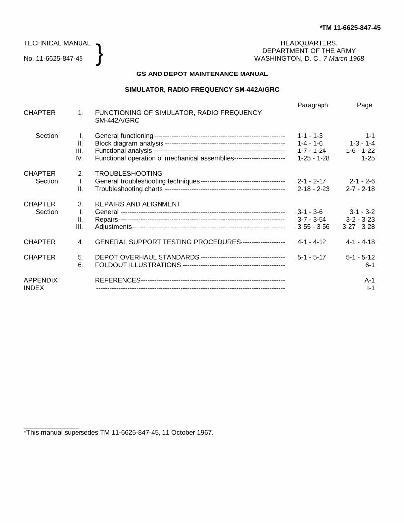
*TM 11-6625-847-45
TECHNICAL MANUAL HEADQUARTERS,DEPARTMENT OF THE ARMY
No. 11-6625-847-45 WASHINGTON, D. C., 7 March 1968
GS AND DEPOT MAINTENANCE MANUAL
SIMULATOR, RADIO FREQUENCY SM-442A/GRC
Paragraph PageCHAPTER 1. FUNCTIONING OF SIMULATOR, RADIO FREQUENCY
SM-442A/GRC
Section I. General functioning ----------------------------------------------------------- 1-1 - 1-3 1-1II. Block diagram analysis ------------------------------------------------------ 1-4 - 1-6 1-3 - 1-4
III. Functional analysis ----------------------------------------------------------- 1-7 - 1-24 1-6 - 1-22IV. Functional operation of mechanical assemblies----------------------- 1-25 - 1-28 1-25
CHAPTER 2. TROUBLESHOOTINGSection I. General troubleshooting techniques -------------------------------------- 2-1 - 2-17 2-1 - 2-6
II. Troubleshooting charts ------------------------------------------------------ 2-18 - 2-23 2-7 - 2-18
CHAPTER 3. REPAIRS AND ALIGNMENTSection I. General -------------------------------------------------------------------------- 3-1 - 3-6 3-1 - 3-2
II. Repairs--------------------------------------------------------------------------- 3-7 - 3-54 3-2 - 3-23III. Adjustments--------------------------------------------------------------------- 3-55 - 3-56 3-27 - 3-28
CHAPTER 4. GENERAL SUPPORT TESTING PROCEDURES-------------------- 4-1 - 4-12 4-1 - 4-18
CHAPTER 5. DEPOT OVERHAUL STANDARDS -------------------------------------- 5-1 - 5-17 5-1 - 5-126. FOLDOUT ILLUSTRATIONS ---------------------------------------------- 6-1
APPENDIX REFERENCES----------------------------------------------------------------- A-1INDEX ------------------------------------------------------------------------------------- I-1
_______________*This manual supersedes TM 11-6625-847-45, 11 October 1967.
TM 11-6625-847-45
CHAPTER 1FUNCTIONING OF SIMULATOR, RADIO
FREQUENCY SM-422A/GRC
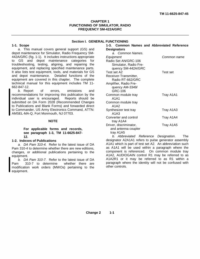
Section I. GENERAL FUNCTIONING1-1. Scope
a. This manual covers general support (GS) anddepot maintenance for Simulator, Radio Frequency SM-442A/GRC (fig. 1-1). It includes instructions appropriateto GS and depot maintenance categories fortroubleshooting, testing, aligning, and repairing theequipment, and replacing specified maintenance parts.It also lists test equipment, tools, and materials for GSand depot maintenance. Detailed functions of theequipment are covered in this chapter. The completetechnical manual for this equipment includes TM 11-662-847-12.
b. Report of errors, omissions andrecommendations for improving this publication by theindividual user is encouraged. Reports should besubmitted on DA Form 2028 (Recommended Changesto Publications and Blank Forms) and forwarded directto Commander, US Army Electronics Command, ATTN:AMSEL-MA-Q, Fort Monmouth, NJ 07703.
NOTE
For applicable forms and records,see paragraph 1-3, TM 11-6625-847-12.
1-2. Indexes of Publicationsa. DA Pam 310-4. Refer to the latest issue of DA
Pam 310-4 to determine whether there are new editions,changes, or additional publications pertaining to theequipment.
b. DA Pam 310-7. Refer to the latest issue of DAPam 310-7 to determine whether there aremodification work orders (MWOs) pertaining to theequipment.
1-3. Common Names and Abbreviated ReferenceDesignators
a. Common Names.Equipment Common nameRadio Set AN/GRC-106
Simulator, Radio Fre-quency SM-442A/GRC
Test set A2 Test setReceiver-Transmitter,
Radio RT-662/GRCAmplifier, Radio Fre-
quency AM-3349/GRC-106
Common module tray Tray A1A1A1A1
Common module trayA1A2
Synthesizer test tray Tray A1A3A1A3
Converter and control Tray A1A4tray A1A4
Driver, discriminator, Tray A1A5and antenna couplertray A1A5b. Abbreviated Reference Designation. The
designator A2A1A1 refers to pulse generator assemblyA1A1 which is part of test set A2. An abbreviation suchas A1A1 will be used within a paragraph where thecomponent is referenced. On common module trayA1A2, AUDIOGAIN control R1 may be referred to asA1A2R1 or it may be referred to as R1 within aparagraph where the identity will not be confused withother controls.
Change 2 1-1
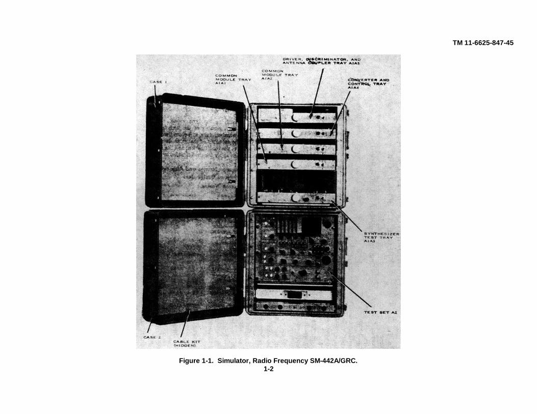
TM 11-6625-847-45
Figure 1-1. Simulator, Radio Frequency SM-442A/GRC.1-2
TM 11-6625-847-45
Section II. BLOCK DIAGRAM ANALYSIS
1-4. General
a. The purpose of Simulator, Radio FrequencySM-442A/GRC is to provide all the necessary stimuluscontrol, test points, electrical connections, mechanicalcoupling, power source, and resistive power loads fortesting Radio Set AN/GRC-106. With standard externaltest equipment, both GS and depot categories of testingcan be performed on either the modules orsubassemblies of the AN/GRC-106 or performance testscan be made of Receiver-Transmitter, Radio RT-662/GRC and Amplifier, Radio Frequency AM-3349/GRC-106 units separately or as a complete AN/GRC-106.
b. When conducting system tests of the AN/GRC-106, the units being tested are connected directly to thetest set A2 by test cables. For module testing of theAN/GRC-106, the appropriate test fixture tray isrequired. Direct current (dc) and alternating current(ac), mechanical coupling, switching information, andthe stimulus that is normally supplied by a completeradio set are supplied by the test fixture tray to themodule being tested.
1-5. Block Diagram Analysis of System Testing
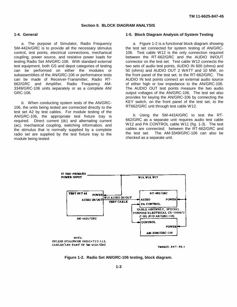
a. Figure 1-2 is a functional block diagram showingthe test set connected for system testing of AN/GRC-106. Test cable W12 is the only connection requiredbetween the RT-662/GRC and the AUDIO IN/OUTconnector on the test set. Test cable W12 connects thetwo sets of audio test points, AUDIO IN 600 (ohms) and50 (ohms) and AUDIO OUT 2 WATT and 10 MW, onthe front panel of the test set, to the RT-662/GRC. TheAUDIO IN test points connect an external audio sourceof either high or low impedance to the AN/GRC-106.The AUDIO OUT test points measure the two audiooutput voltages of the AN/GRC-106. The test set alsoprovides for keying the AN/GRC-106 by connecting theKEY switch, on the front panel of the test set, to theRT662/GRC unit through test cable W12.
b. Using the SM-442A/GRC to test the RT-662/GRC as a separate unit requires audio test cableW12 and PA CONTROL cable W11 (fig. 1-3). The testcables are connected: between the RT-662/GRC andthe test set. The AM-3349/GRC-106 can also bechecked as a separate unit.
Figure 1-2. Radio Set AN/GRC-106 testing, block diagram.
1-3
TM 11-6625-847-45
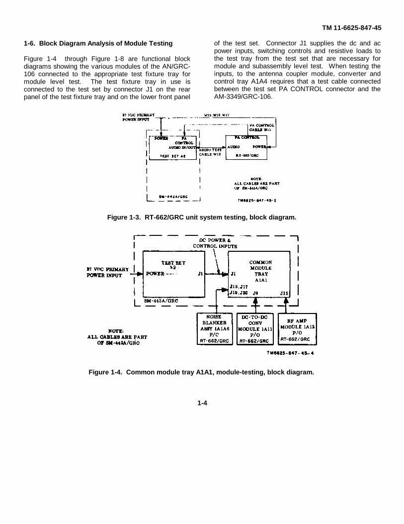
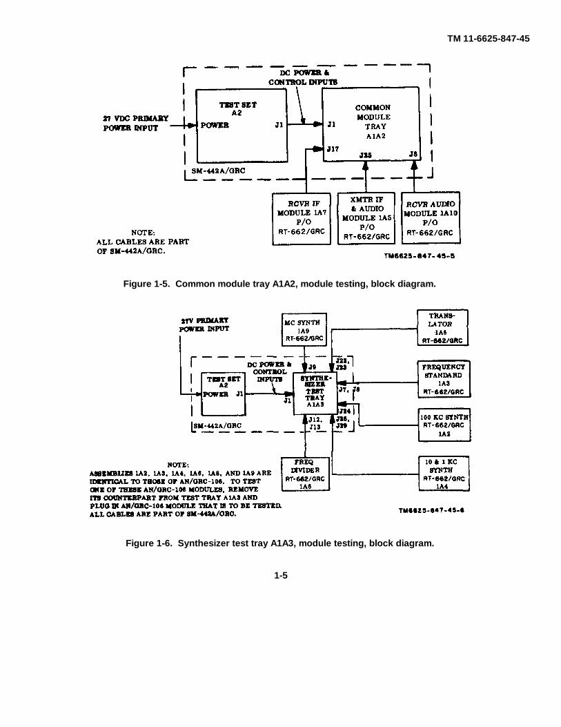
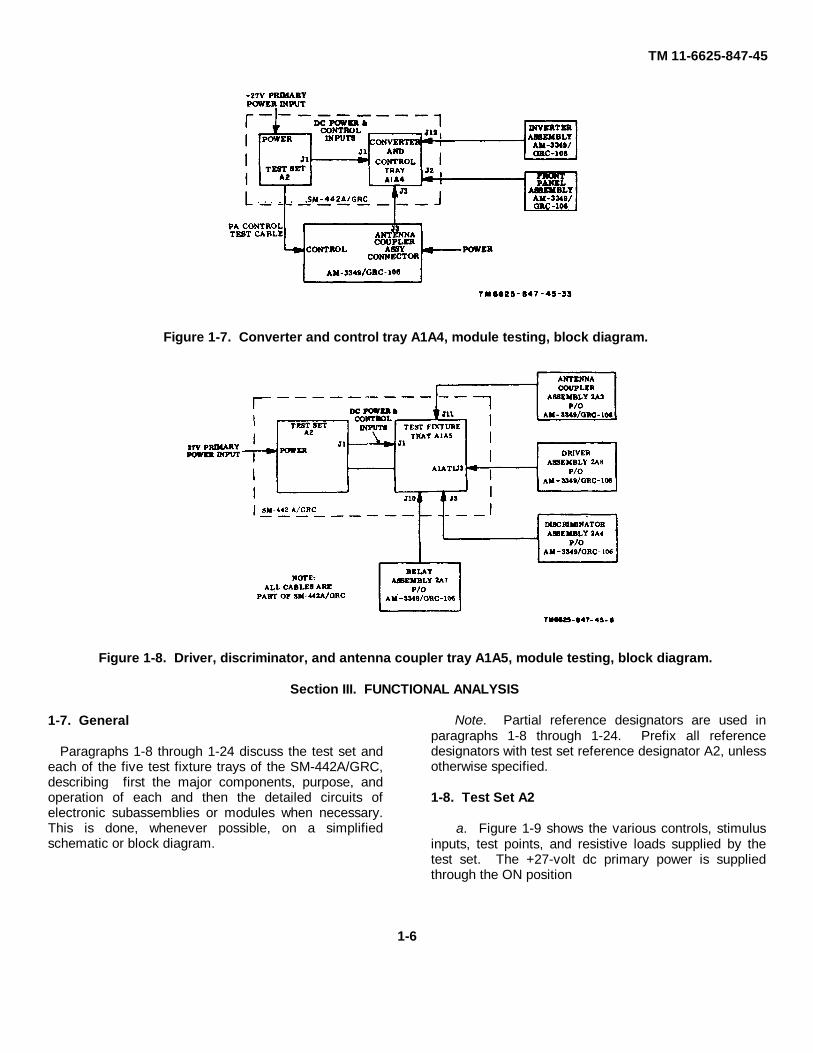
1-6. Block Diagram Analysis of Module Testing
Figure 1-4 through Figure 1-8 are functional blockdiagrams showing the various modules of the AN/GRC-106 connected to the appropriate test fixture tray formodule level test. The test fixture tray in use isconnected to the test set by connector J1 on the rearpanel of the test fixture tray and on the lower front panel
of the test set. Connector J1 supplies the dc and acpower inputs, switching controls and resistive loads tothe test tray from the test set that are necessary formodule and subassembly level test. When testing theinputs, to the antenna coupler module, converter andcontrol tray A1A4 requires that a test cable connectedbetween the test set PA CONTROL connector and theAM-3349/GRC-106.
Figure 1-3. RT-662/GRC unit system testing, block diagram.
Figure 1-4. Common module tray A1A1, module-testing, block diagram.
1-4
TM 11-6625-847-45
Figure 1-5. Common module tray A1A2, module testing, block diagram.
Figure 1-6. Synthesizer test tray A1A3, module testing, block diagram.
1-5
TM 11-6625-847-45
Figure 1-7. Converter and control tray A1A4, module testing, block diagram.
Figure 1-8. Driver, discriminator, and antenna coupler tray A1A5, module testing, block diagram.
Section III. FUNCTIONAL ANALYSIS
1-7. General
Paragraphs 1-8 through 1-24 discuss the test set andeach of the five test fixture trays of the SM-442A/GRC,describing first the major components, purpose, andoperation of each and then the detailed circuits ofelectronic subassemblies or modules when necessary.This is done, whenever possible, on a simplifiedschematic or block diagram.
Note. Partial reference designators are used inparagraphs 1-8 through 1-24. Prefix all referencedesignators with test set reference designator A2, unlessotherwise specified.
1-8. Test Set A2
a. Figure 1-9 shows the various controls, stimulusinputs, test points, and resistive loads supplied by thetest set. The +27-volt dc primary power is suppliedthrough the ON position
1-6
TM 11-6625-847-45
of POWER switch A1S2 to SERV SEL switch A1S1,through thermal activated switch S1 to blower motors B1and B2, and to test set connector J1. The SERV SELswitch controls the mode of operation of the test set inthe first four positions, OFF, OVEN ON, STBY, andSSB/NSK, and stimulates the functions that arenormally supplied to test set connector J1 by theSERVICE SELECTOR switch on the front panel of theRT-662/GRC in positions OFF, OVEN ON, STBY,SSB/NSK, FSK, AM and CW. The SERV SEL switch inany position other than OFF supplies +27-volt dcprimary power to the regulator section of dc-to-dcconverter and regulator module A3. Figure 6-3 is thetest set schematic diagram.
b. Module A3 (fig. 6-3) regulates the +27-volt dcprimary power to +20 volts dc. The ON position of thePOWER switch on one of the module testing trays,when connected to the test set, supplies +27-volt dcprimary power to the converter section of module A3.The converter section of module A3 converts the +27-volt dc primary power to + 125 volts dc, -33 volts dc and6.3 volts ac. The + 20-volt dc output of module A3 isused on the test set as B+ supply voltage forintermediate frequency (if) oscillator modules A1A2,A1A3, and A1A4. For operating voltages, pulsegenerator module A1A1 requires the +20-volt dc and the*33-volt dc outputs for the dc-to-dc converter andregulator module A3.
c. Two-tone select switch A1S8 controls the outputof the three IF oscillator modules, A1A2, A1A3, andA1A4, by switching the +20-volt dc B + supply voltageeither on or off to one or more of the modules. ModulesA1A2 and A1A3, when selected supply 1.7525-megacycle (mc) and 1.7515-mc inputs to mixerassembly A1A5. The output of the mixer assembly iseither 1.7525 mc or 1.7515 mc, or both, depending onthe position of two-tone selector switch A1S8. Theoutput of the mixer assembly is connected to connectorJ1. With common module tray A1A2 (fig. 68) connectedto the test set, the output of the mixer assembly can beswitched from if. oscillator modules A1A2 and A1A3 toan external two-tone signal generator source by placing
RCVR IF AGC SYNC switch A2S6 on tray A1A2 to OFF.The output of IF oscillator module A1A4, when selectedby switch A1S8, is 1.7500 mc and is connected directlyto connector J1.
d. Megacycle frequency selection is accomplishedby MC FREQ 10 MC switch A1S9, .1 MC switch A1S11,and .1 MC switch A1S10. These switches are used tocontrol the position of the mc frequency couplers oncommon module tray A1A1 and synthesizer test trayA1A3 and provide the five-wire coding inputs to the AM-3349/GRC-106 at PA CONTROL connector A1J12.
e. Dc-to-dc converter module A2 on the test set iscontrolled by an interlock jumper wire on connector J1of driver, discriminator, and antenna coupler tray A1A5.When tray A1A5 is connected to the test set, the +27-volt dc primary power is supplied to module A2 forconversion to + 200 volts dc. The +200-volt dc power isthen connected back to tray A1A5 for module excitation.
f. The resistive loads supplied by the test set tothe module testing tray are as follows: a 2,400-volt dcload, a 500-volt dc load, a 200-ohm, 250-watt resistor,and a 420-ohm, 250-watt resistor. The 2,400-volt dcload is controlled by seven-position 2400 VDC LOADswitch A1S3 by selecting the number of resistors inparallel with the input leads of the load. The 500-volt dcload is controlled by 500 VDC LOAD switch A1S7 aseither a low or high current load by the paralleling of twofixed resistors across the input leads.
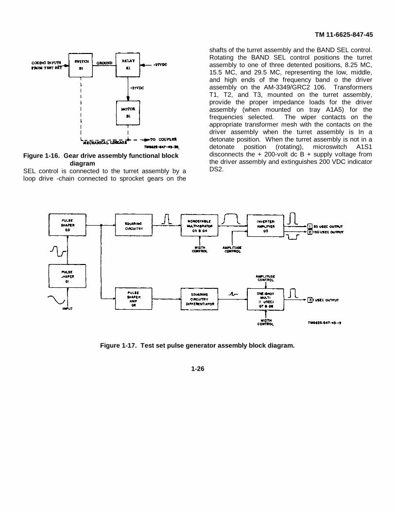
g. Pulse generator module A1A1 supplies a 1microsecond (usec) pulse and either an 85-usec positivepulse or a 150-usec negative pulse to the front panel ofthe test set at OUTPUTS connectors 1, 2, and 3,respectively. The pulse generator is triggered by anexternal audio signal generator connected to the PULSEGENERATOR INPUT connector. The frequency of theaudio signal generator determines the pulse repetitionrate of the pulse generator.
h. When in the TUNE position, XMIT STATUSswitch A1S5 supplies a ground to test set connector J1.In the ON position, KEY switch A1S6 supplies a groundand +20 volts dc to two pins of connector J1 and aground to connector A1J4. The REC XMIT switch re-
Change 2 1-7
TM 11-6625-847-45
Figure 1-9. Test set, block diagram.
Change 2 1-8
TM 11-6625-847-45
verses + 20 volts dc and ground on the two pins ofconnector J1 when switched from either REC or XMIT.
1-9. Pulse Generator Subassembly A2A1A1(fig. 1-17, fig. 3-10, and fig. 6-4)
Note. Where partial reference designators areused, prefix with test set and pulse generator referencedesignator A2A1A1, unless otherwise specified.
a. The function of pulse generator subassemblyA2A1A1 is to supply to separate connectors on the frontpanel of the test set with a 1-usec wide positive pulseand either a 150-usec negative pulse or an 85-usecpositive pulse. Front panel controls on the test setadjust the width and amplitude of the 1-usec pulse andthe width and amplitude of either the 85-usec wide pulseor the 150-usec wide pulse. The pulse repetition rate ofthe pulse generator is controlled by the frequency of theexternal audio signal generator connected to INPUTconnector J1.
b. The input audio signal at INPUT connector J1 isconnected to the base of first pulse shaper transistorA1Q1 by capacitor A1C1. Transistors A1Q1 and A1Q2are utilized as a pulse shaping circuit to shape the inputsine wave into a square wave. The output of the pulseshaping circuitry, at the collector of A1Q2, is the inputto the base of transistor A1Q6 and to capacitor A1C3.Diode A1CR3 connected between capacitor A1C3 andthe collector of transistor A1Q3 couples the positiveportion of the square wave as the trigger input to themonostable multivibrator consisting of transistors A1Q3and A1Q4. The negative portion of the square waveinput at capacitor A1C3 is shunted to ground by diodeA1CR2. Each positive trigger input to the multivibratorgenerates an output pulse by switching the multivibratorfrom the normal stable state to the unstable state for alength of time depending on the setting of WIDTHcontrol resistor R2. The WIDTH control is used to setthe output of the multivibrator for either an 85-usec or(150-usec) duration pulse. The negative output pulse ofthe multivibrator, at the collector of transistor A1Q4, isthe input to the base of inverter amplifier transistorA1Q5. The amplitude of the pulse output of A1Q5 iscontrolled by basebiasing resistor AMPLITUDE controlR1. The negative (150-usec) output pulse is coupled to
connector J2 from the emitter of A1Q5 by capacitorA1C6. The positive (85 usec) output pulse is coupled bycapacitor A1C7 from the collector of A1Q5 to connectorJ3.
c. The square wave output of transistor A1Q2 isfurther amplified and shaped by transistor A1Q6. Theoutput of A1Q6 is differentiated into a positive andnegative pulse by capacitor A1C9 and resistor A1R18.The negative pulse is shunted to ground by diodeA1CR4. The positive pulse, coupled by diode A1CR5, isthe input to a Schmitt trigger multivibrator consisting oftransistors A1Q7 and A1Q8. The Schmitt trigger circuitprovides a standard pulse output for each positive inputtrigger pulse. Variable WIDTH control resistor R4controls the duration of the output pulse of the Schmitttrigger to 1-usec. The amplitude of the 1-usec outputpulse is controlled by coupling a portion of the pulsedeveloped across collector load AMPLITUDE resistorR3 and coupled by capacitor A1C12 to connector J4.
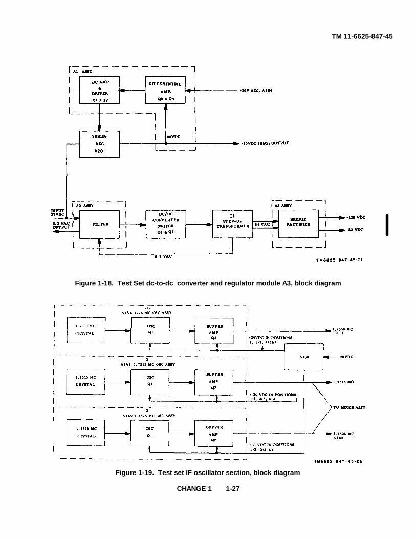
1-10. Dc-to-Dc Converter and Regulator ModuleA2A3(fig. 1-18 and fig. 6-5)
Note. Where only partial reference designator areused, prefix with test set and dc-to-dc converter andregulator module reference designator A2A3, unlessotherwise specified.
a. The function of dc-to-dc converter and regulatormodule A2A3 is to produce all operating voltagesrequired by the SM-442A/ GRC with the exception of the+ 27-volt dc primary power.
b. In the regulator section, the +27-volt dc isapplied to the collector of transistor 1A1Q1 on thechassis of the test set and to pin 13 of J2. The effectivecollector-to-emitter resistance of test set transistor1A1Q1, in series with the +27-volt dc line, drops thevoltage to a constant +20 volts dc for any given currentrequired by the external circuits. The value of the seriesresistance is determined by the rate of conduction oftest set transistor 1A1Q1, controlled by the regulatorcircuit. The differential amplifier, consisting oftransistors A1Q3 and A1Q4, compares the output fromtest set transistor
1-9

TM 11-6625-847-45
1A1Q1 to the reference established by 4.7-volt Zenerdiode A1VR2. The output at the emitter of test settransistor 1A1Q1 is developed across the voltage divider,consisting of resistors A1R7, 1A1R4, and A1R8. Variableresistor 1A1R4 on the front panel of the test set providesadjustments of the base voltage of A1Q4 to maintain aconstant output voltage from the regulator with variationsin component values because of age and temperature.Assume that the + 20-volt dc output instantaneouslyincreases to +22 volts dc. The voltage across the voltagedivider will increase the base bias of transistor A1Q4.Transistor A1Q4 will have an increased rate ofconduction, increasing the voltage developed acrossresistor A1R6. This decreases the forward-biasing oftransistor A1Q3, increasing the voltage at the collector oftransistor A1Q3. This increased voltage will decrease theforward bias on dc amplifier A1Q2, increasing the voltageon the collector of dc amplifier A1Q2. The base voltageof dc amplifier A1Q2 is stabilized by Zener diode A1VR1;therefore, the emitter-to-base voltage on driver A1Q1 willdecrease, decreasing the voltage on the collector of driverA1Q1. The collector voltage of driver A1Q1 is the basebias for test set transistor A1Q1; therefore, the decreaseat the collector of driver A1Q1 causes test set -transistorA1Q1 to conduct less. This action increases the collector-to-emitter resistance to drop the voltage back to +20 voltsdc. A similar sequence of events will occur if the +20volts dc decreases; however, the reverse will occur in allthe circuits to increase the conduction rate of test settransistor A1Q1 and thereby decrease the collector-to-emitter resistance to increase the voltage at the emitter oftest set transistor 1A1Q1 to +20 volts dc. Capacitor A1C5provides filtering for the + 20 volt dc output line.Capacitor A1C4 provides filtering feedback for transistorA1Q4; therefore, any ripple on the + 20-volt dc output linewill be fed 'back into the regulator circuit, ,and. in turn, totest transistor 1A1Q1 which is 180° out-of-phase withitself and allow the ripple to be canceled. CapacitorsA1C1, A1C2, and A1C3 provide high frequency filtering.If the + 20-volt dc line becomes short-circuited, theresulting ground with forward-bias diode A1CR1, shutting
off dc amplifier A1Q2, which, in turn, shuts off driverA1Q1 and test transistor 1A1Q1. When the short-circuit isremoved, the regular will recover and resume regulatingaction.
c. The dc-to-dc converter is a saturable coreoscillator used to produce the dc and ac operatingvoltages required by the SM-442A/ GRC. The +27-volt dcprimary power is applied to pin 7 of connector J2, fromwhich it is applied through a pi-section filter network to pin9 of transformer T1. The pi-section filter consists ofinductor L1 and capacitors A2C1, A2C2, A2C3, andA2C4. The +27-volt dc is applied through the transformerwinding to the collector of both transistors Q1 and Q2 andthrough resistor A2R1, the transformer winding, andresistors R1 and R2 to the bases of transistors Q1 andQ2. The differences in the two transistors will cause oneof them to turn on first. Assume that transistor Q1 turnson first. Application of +27 volts dc then will induce avoltage in the windings of transformers T1 with thefollowing polarities: pin 9, plus; pin 2, minus; pin 1, plus;and pin 3, minus; X therefore, transistor Q1 is moreforward-biased by the positive voltage on its base and isdriven toward saturation. Transistor Q1 will conduct intosaturation, at which time the magnetic field created in thewindings will collapse since the current becomes constant.The polarities of the windings will be reversed, turningtransistor Q2 on. This action will continue, producing asquare wave ac signal across the primary of transformerT1. Resistors R1 and R2 are base current limitingresistors. Diode A2CR1 will clamp pin 10 of transformerT1 at ground so that maximum drive can be applied to theconduction transistor to drive it into saturation.
d. The 54-volt ac output from dc-tide converterswitch Q1, Q2 is stepped-down in transformer winding 4-5, filtered, and applied to pins 1 and 9 of connector J2 asu.3 volts ac. The 54-volt ac is stepped-up by transformerwinding 6-12, full-wave rectified by diodes A3CR1 throughA3CR4, filtered, and applied to pin 6 of connector J2 asthe + 125-volt dc
1-10
TM 11-6625-847-45
output. The 54-volt ac is stepped-up by transformerwinding 7-8, full-wave rectified by diodes A3CR5 throughA3CR8, regulated by 33-volt Zener diode A3VR1, filtered,and applied to pin 14 of connector J2.
Note: Figure 6-2 contains the charts for MIL Standardresistors, capacitors, and inductors.
1-1 1. IF Oscillator Circuit(fig. 1-19, fig. 6-3, and fig. 6-6)
Note. Where partial reference designators are used,prefix with test set reference designator AZ, and theappropriate IF oscillator module presence designatorA1A2, A1A3, or A1A4, for example: A2A1A2.
a. The function of the IF oscillator circuitry is toprovide either a two-tone or single-tone IF frequency toconnector A2J1 on the test set. The IF oscillator circuitconsists of three crystal-controlled oscillators modulesA2A1A2, A2A1A3, and A2A1A4 and two-tone selectorswitch A2A1S8. The two-tone selector switch selects theoutput of the IF oscillator circuit by switching the + 20-vkdc B + supply voltage to the oscillator module selected,energizing the oscillator. Oscillator module A2A1A4,when selected, provides a 1.7500-mc output to test setconnector A2J1. Oscillator modules A2A1A2 andA2A1A3 provide 1.7525-mc and 1.7515-mc inputs,respectively, to two-tone mixer assembly A2A1A5.
b. Oscillator modules A2A1A2, A2A1A3, andA2A1A4 are identical in operation and in circuitry with theexception of the frequency of the crystals. Each oscillatormodule contains a crystal controlled transistor oscillatorA1Q1 and a buffer amplifier A1Q2. Oscillation oftransistor A1Q1 is sustained by coupling the in-phasesignal from the emitter of A1Q1 through resistor A1R7and capacitor A1C1 to the base of A1Q1. A positiveoutput trigger from the crystal-driven tank circuitconsisting of capacitors all, A1C2, and diode A1CR1 iscoupled to the base of A1Q1 through diode A1CR2 andA1C4 to frequency-stabilize the OSCILLATOR The -inputof oscillator A1Q1 is the input at the base of bufferamplifier A1Q2. Variable resistor A1R1 in the emitter ofA1Q2 controls the output amplitude of the buffer amplifierat output jack J1 for module A2A1A4. For modules
A2A1A2 and A2A1A3, the output is the input of two-tonemixer assembly A2A1A5 (fig. 6-3).
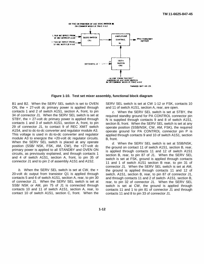
1-1 2. Mixer Assembly A1A5(fig. 1-10 and fig. 6-3)
Note. Where partial reference designators are used,prefix with test set and mixer assembly referencedesignator A2A1A5, unless otherwise specified, forexample: A2A1A5 C1.
The input from IF oscillators modules A2A1A2 andA2A1A3 are combined by the common tie point ofcapacitors C1 and C2 and by diode CR1. Diode CR1 isutilized as a diode switch and controlled by the RCVR IFAGC SYNC switch on tray A1A2. When the RCVR IFAGC SYNC switch is set to ON, +20-volt dc is supplied tothe anode of diode CR1 through resistor R5, forward-biasing the diode into conduction. When diode CR1 isforward based, the input signals at J3 and J4 are coupledto AMPLITUDE control resistor R1 through diode CR1and capacitor C5. Resistor R1 is used to control theoutput level of the mixer assembly. Placing the RCVR IFAGC SYNC switch on tray A1A2 to OFF removes theforward-bias from diode CR1, disconnecting the inputsignals from J3 and J4 from J2 and OUT connector J5,and forward-biasing diode CR2 into conduction. Whendiode CR2 is forward-biased, the external if. signalconnected to IN connector J1 of the mixer assembly iscoupled as the output of the mixer assembly throughcapacitor C3, diode CR2, and capacitor C4 to connectorJ2 and OUT connector J5. Resistor R1 controls theamplitude by shunting a portion of the input signal toground.
1-13. SERV SEL Switch(fig. 6-3)
Note. Prefix reference designators with test set referencedesignator A2, unless otherwise specified.
a. The +27-volt dc applied to pins A and B ofPOWER connector A1J1 is applied through the ONposition of POWER switch A1S2; through 10 AMP fuseA1F1; to contact 1 of switch A1S1, section A, front; toindicator A1DS1; and through switch S1 to fan motors
Change 1 1-11
TM 11-6625-847-45
Figure 1-10. Test set mixer assembly, functional block diagram
B1 and B2. When the SERV SEL switch is set to OVENON, the + 27-volt dc primary power is applied throughcontacts 1 and 2 of switch A1S1, section A, front, to pin34 of connector J1. When the SERV SEL switch is set atSTBY, the + 27-volt dc primary power is applied throughcontacts 1 and 3 of switch A1S1, section A, front, to pin29 of connector J1, to contact 9 of REC XMIT switchA1S4, and to dc-to-dc converter and regulator module A3.This voltage is used in dc-to-dc converter and regulatormodule A3 to energize the +20-volt dc regulator circuits.When the SERV SEL switch is placed at any operateposition (SSB/ NSK, FSK, AM, CW), the +27-volt dcprimary power is applied to all STANDBY and OVEN ONcircuits, as previously explained, and through contacts 1and 4 of switch A1S1, section A, front, to pin 35 ofconnector J1 and to pin 2 of assembly A1S1 and A1S2.
b. When the SERV SEL switch is set at CW, the +20-volt dc output from transistor Q1 is applied throughcontacts 5 and 6 of switch A1S1, section A, rear, to pin 30of connector J1. When the SERV SEL switch is set atSSB/ NSK or AM, pin 75 of J1 is connected throughcontacts 10 and 11 of switch A1S1, section A, rear, tocontact 10 of switch A1S1, section C, front. When the
SERV SEL switch is set at CW 1-12 or FSK, contacts 10and 11 of switch A1S1, section A, rear, are open.
c. When the SERV SEL switch is set at STBY, therequired standby ground for PA CONTROL connector pinN is supplied through contacts 9 and 8 of switch A1S1,section B, front. When the SERV SEL switch is set at anyoperate position (SSB/NSK, CW, AM, FSK), the requiredoperate ground for PA CONTROL connector pin P isapplied through contacts 9 and 10 of switch A1S1, sectionB, front.
d. When the SERV SEL switch is set at SSB/NSK,the ground on contact 11 of switch A1S1, section B, rear,is applied through contacts 11 and 12 of switch A1S1section B, rear, to pin 87 of J1. When the SERV SELswitch is set at FSK, ground is applied through contacts11 and 1 of switch A1S1 section B rear, to pin 31 ofconnector J1. When the SERV SEL switch is set at AM,the ground is applied through contacts 11 and 12 ofswitch. A1S1, section B, rear, to pin 87 of connector J1,and through contacts 11 and 2 of switch- A1S1, section B,rear, to pin 32 of connector J1. When the SERV SELswitch is set at CW, the ground is applied throughcontacts 11 and 1 to pin 81 of connector J1 and throughcontacts 11 and 8 to pin 33 of connector J1.
1-12
TM 11-6625-847-45
e.When the SERV SEL switch is set to SSB/NSK or AM,pin 86 of connector J1 is connected through contacts 8and 9 or 8 and 11 of switch A1S1, section C, front, to pin79 of connector J1. When the SERV SEL switch is setto FSK, pin 86 of connector J1 is connected throughcontacts 8 and 10 of switch A1S1, section C, front, topin 76 of connector J1 is connected through contacts 8and 10 of switch A1S1 section C, front, to pin 76 ofconnector J1. When the SERV SEL switch is set toCW, pin 86 of connector J1 is connected throughcontacts 8 and 12 of switch A1S1, section C, front, topin 88 of connector J1.
1-14. Mc Frequency Selection Circuit (fig. 6-3)
NOTEPrefix all reference designators withthe test set reference designator A2,unless otherwise specified.
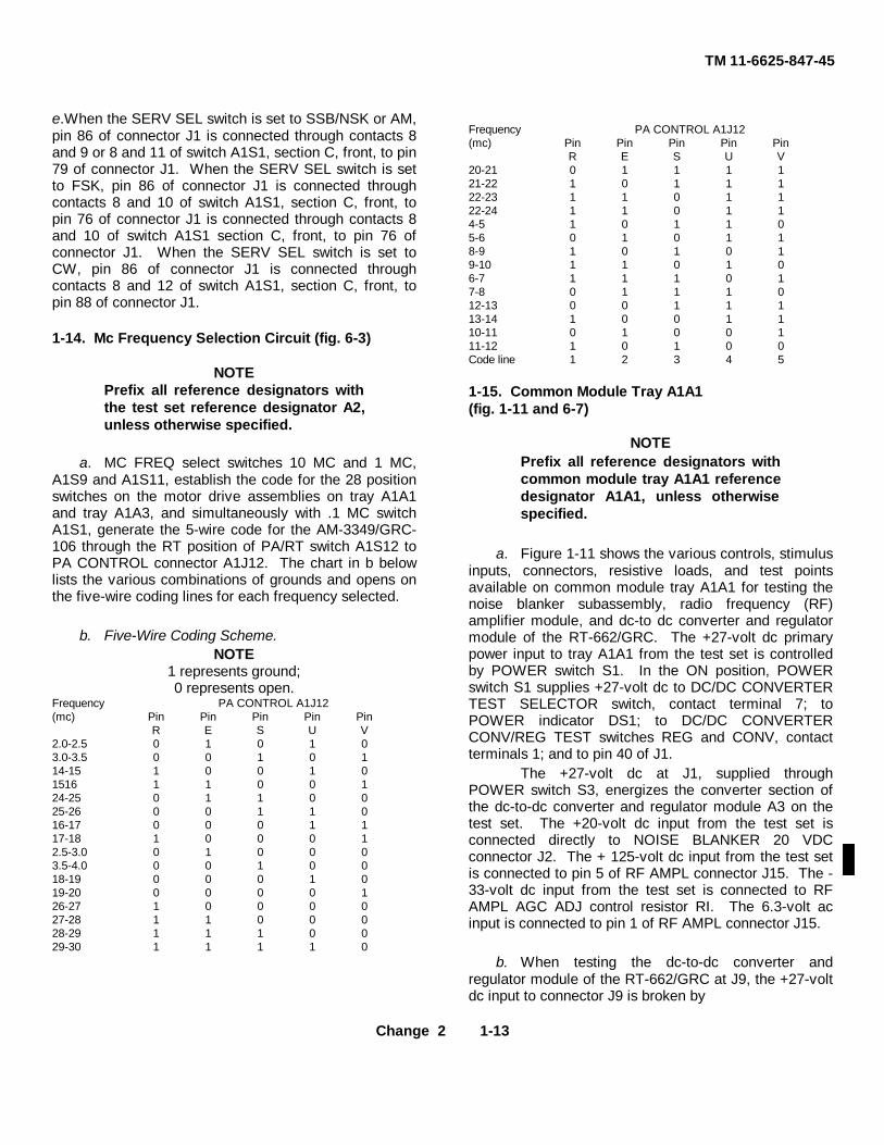
a. MC FREQ select switches 10 MC and 1 MC,A1S9 and A1S11, establish the code for the 28 positionswitches on the motor drive assemblies on tray A1A1and tray A1A3, and simultaneously with .1 MC switchA1S1, generate the 5-wire code for the AM-3349/GRC-106 through the RT position of PA/RT switch A1S12 toPA CONTROL connector A1J12. The chart in b belowlists the various combinations of grounds and opens onthe five-wire coding lines for each frequency selected.
b. Five-Wire Coding Scheme.NOTE
1 represents ground;0 represents open.
Frequency PA CONTROL A1J12(mc) Pin Pin Pin Pin Pin
R E S U V2.0-2.5 0 1 0 1 03.0-3.5 0 0 1 0 114-15 1 0 0 1 01516 1 1 0 0 124-25 0 1 1 0 025-26 0 0 1 1 016-17 0 0 0 1 117-18 1 0 0 0 12.5-3.0 0 1 0 0 03.5-4.0 0 0 1 0 018-19 0 0 0 1 019-20 0 0 0 0 126-27 1 0 0 0 027-28 1 1 0 0 028-29 1 1 1 0 029-30 1 1 1 1 0
Frequency PA CONTROL A1J12(mc) Pin Pin Pin Pin Pin
R E S U V20-21 0 1 1 1 121-22 1 0 1 1 122-23 1 1 0 1 122-24 1 1 0 1 14-5 1 0 1 1 05-6 0 1 0 1 18-9 1 0 1 0 19-10 1 1 0 1 06-7 1 1 1 0 17-8 0 1 1 1 012-13 0 0 1 1 113-14 1 0 0 1 110-11 0 1 0 0 111-12 1 0 1 0 0Code line 1 2 3 4 5
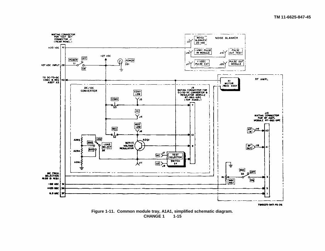
1-15. Common Module Tray A1A1(fig. 1-11 and 6-7)
NOTEPrefix all reference designators withcommon module tray A1A1 referencedesignator A1A1, unless otherwisespecified.
a. Figure 1-11 shows the various controls, stimulusinputs, connectors, resistive loads, and test pointsavailable on common module tray A1A1 for testing thenoise blanker subassembly, radio frequency (RF)amplifier module, and dc-to dc converter and regulatormodule of the RT-662/GRC. The +27-volt dc primarypower input to tray A1A1 from the test set is controlledby POWER switch S1. In the ON position, POWERswitch S1 supplies +27-volt dc to DC/DC CONVERTERTEST SELECTOR switch, contact terminal 7; toPOWER indicator DS1; to DC/DC CONVERTERCONV/REG TEST switches REG and CONV, contactterminals 1; and to pin 40 of J1.
The +27-volt dc at J1, supplied throughPOWER switch S3, energizes the converter section ofthe dc-to-dc converter and regulator module A3 on thetest set. The +20-volt dc input from the test set isconnected directly to NOISE BLANKER 20 VDCconnector J2. The + 125-volt dc input from the test setis connected to pin 5 of RF AMPL connector J15. The -33-volt dc input from the test set is connected to RFAMPL AGC ADJ control resistor RI. The 6.3-volt acinput is connected to pin 1 of RF AMPL connector J15.
b. When testing the dc-to-dc converter andregulator module of the RT-662/GRC at J9, the +27-voltdc input to connector J9 is broken by
Change 2 1-13
TM 11-6625-847-45
DC/DC CONVERTER CONV/REG TEST switches REGand CONV and caused to flow through an externalammeter. The ammeter is connected across test pointsHI and CONV LOW for current measurements of theconverter section and test points HI and REG LOW forcurrent measurements of the regulator section of themodule DC/DC CONVERTER TEST SELECTOR switchS4 controls the pin selection of DC/DC CONVERTERtest points HI and LO for voltage measurements underspecified loads at the connector pins J9 as follows:position 1 monitors the +27-volt dc input voltage fromthe test set; position 2 connects the test points to theoutput of the +20-volt dc regulator at the emitter oftransistor A2Q1; position 3 monitors the + 125-volt dc atpin 6 of J9; position 4 monitors the -33 volt dc at pin 14of J9, position 5 connects the test points across 6.3-voltac at pins 1 and 9 of J9. Transistor A2Q1 replaces the+20-volt dc series regulator transistor of the dc-to-dcconverter and regulator module that is mounted on thechassis of the RT-162/GRC unit and disconnected fromthe regulator section when the module is removed. Theoutput of the +20-volt dc regulator is controlled by three-position DC/DC CONVERTER LOAD SELECT switchS6. The positions of the LOAD SELECT switch aredesignated 100, 500, and 600 for resistive loadsproviding current drains of 100 milliamperes (ma), 500ma, and 600 ma, respectively. Test point J11 is formeasuring the output voltage of the +20-volt dcregulator.
c. When testing the noise blanker subassembly ofthe RT-662/GRC, the NOISE BLANKER 1 USECPULSE IN MODULE, PULSE OUT MODULE, andPULSE OUT TEST connectors provide the necessarymating connectors and impedance loads for connectingexternal test equipment with BNC connectors to thenoise blanker subassembly microdot connectors.
d. When testing the RF amplifier module of theRT-62/GRC, the voltage at the wiper of RF AMPL AGCADJ control resistor R1 is connected through the ONcontacts of RF AMP AGC switch N5 as simulatedautomatic gain control (age) voltage to pin 3 of J15.The voltage as controlled by RF AMPL AGC ADJ at pin3 of J15 is the simulated age input voltage to the rfamplifier module.
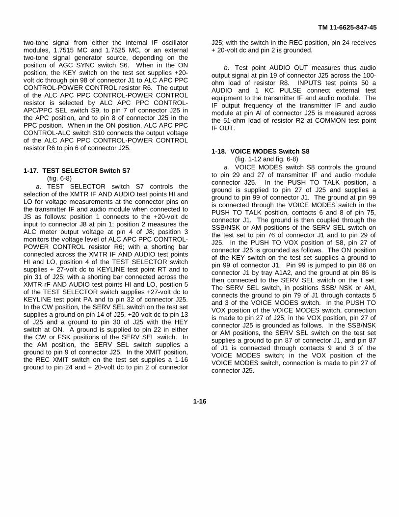
1-16 Common Module Tray A1A2(fig. 1-12 and fig. 6-8)
NOTEPrefix reference designators in tray A1A2 withreference designators A1A2, unless otherwisespecified.
a. Figure 1-12 shows the various controls, stimulusinputs, resistive loads, and test points available on trayA1A2 for testing the receiver IF module, the receiveraudio module, and the transmitter IF and audio moduleof the RT-662/GRC.
b. The +27-volt dc input to tray A1A2 from the testset is controlled by POWER switch S3. In the ONposition, POWER switch S3 supplies the +27-volt dcinput voltage to module connectors J8, pin 8, and J25,pin 28 (fig. 6-8); to POWER indicator DS1; to KCVRAUDIO test point SQUELCH SYNC; and to pin 40 ofconnector J1, energizing the converter section of dc-to-dc converter and regulator module A3 on the test set.The +20-volt dc input from the test set is connecteddirectly to module connectors J8, pin 7; J17, pin 1; andJ25, pin 1; to amplifier assembly A1; and to AGC SYNCswitch S6.
c. When testing the receiver audio module of theRT-662/GRC, the external audio signal from theCOMMON AUDIO 600 Ω IN connector on tray A1A2 isconnected to AUDIO GAIN control variable resistor R1,and through the ON position of the SQUELCH SYNCswitch S1, to receiver audio module connector J8.SQUELCH ON/OFF switch S2 controls the squelchcircuitry of the receiver audio module by supplying aground to pin 13 of J8. The test set SERV SEL switchsupplies a ground to pin 5 of connector J8 when in theFSK and CW positions. OUTPUTS test points 2 WAITand 1O MW monitor the output audio signal of thereceiver audio module.
d. When testing the transmitter IF and audiomodule of the RT-662/GRC, the external audio signalfrom the COMMON AUDIO 600 Ω IN connector isconnected to pin 16 of transmitter IF and audio moduleconnector J25. A 1.750-mc signal is supplied to pin A2of J25 from the test set IF OSCILLATOR (1) 1.75 MCmodule. From the mixer module of the test set, pin A3of connector J25 receives a
1-14
TM 11-6625-847-45
Figure 1-11. Common module tray, A1A1, simplified schematic diagram.CHANGE 1 1-15
TM 11-6625-847-45
two-tone signal from either the internal IF oscillatormodules, 1.7515 MC and 1.7525 MC, or an externaltwo-tone signal generator source, depending on theposition of AGC SYNC switch S6. When in the ONposition, the KEY switch on the test set supplies +20-volt dc through pin 98 of connector J1 to ALC APC PPCCONTROL-POWER CONTROL resistor R6. The outputof the ALC APC PPC CONTROL-POWER CONTROLresistor is selected by ALC APC PPC CONTROL-APC/PPC SEL switch S9, to pin 7 of connector J25 inthe APC position, and to pin 8 of connector J25 in thePPC position. When in the ON position, ALC APC PPCCONTROL-ALC switch S10 connects the output voltageof the ALC APC PPC CONTROL-POWER CONTROLresistor R6 to pin 6 of connector J25.
1-17. TEST SELECTOR Switch S7(fig. 6-8)
a. TEST SELECTOR switch S7 controls theselection of the XMTR IF AND AUDIO test points HI andLO for voltage measurements at the connector pins onthe transmitter IF and audio module when connected toJS as follows: position 1 connects to the +20-volt dcinput to connector J8 at pin 1; position 2 measures theALC meter output voltage at pin 4 of J8; position 3monitors the voltage level of ALC APC PPC CONTROL-POWER CONTROL resistor R6; with a shorting barconnected across the XMTR IF AND AUDIO test pointsHI and LO, position 4 of the TEST SELECTOR switchsupplies + 27-volt dc to KEYLINE test point RT and topin 31 of J25; with a shorting bar connected across theXMTR rF AND AUDIO test points HI and LO, position 5of the TEST SELECTOR switch supplies +27-volt dc toKEYLINE test point PA and to pin 32 of connector J25.In the CW position, the SERV SEL switch on the test setsupplies a ground on pin 14 of J25, +20-volt dc to pin 13of J25 and a ground to pin 30 of J25 with the HEYswitch at ON. A ground is supplied to pin 22 in eitherthe CW or FSK positions of the SERV SEL switch. Inthe AM position, the SERV SEL switch supplies aground to pin 9 of connector J25. In the XMIT position,the REC XMIT switch on the test set supplies a 1-16ground to pin 24 and + 20-volt dc to pin 2 of connector
J25; with the switch in the REC position, pin 24 receives+ 20-volt dc and pin 2 is grounded.
b. Test point AUDIO OUT measures thus audiooutput signal at pin 19 of connector J25 across the 100-ohm load of resistor R8. INPUTS test points 50 aAUDIO and 1 KC PULSE connect external testequipment to the transmitter IF and audio module. TheIF output frequency of the transmitter IF and audiomodule at pin Al of connector J25 is measured acrossthe 51-ohm load of resistor R2 at COMMON test pointIF OUT.
1-18. VOICE MODES Switch S8(fig. 1-12 and fig. 6-8)
a. VOICE MODES switch S8 controls the groundto pin 29 and 27 of transmitter IF and audio moduleconnector J25. In the PUSH TO TALK position, aground is supplied to pin 27 of J25 and supplies aground to pin 99 of connector J1. The ground at pin 99is connected through the VOICE MODES switch in thePUSH TO TALK position, contacts 6 and 8 of pin 75,connector J1. The ground is then coupled through theSSB/NSK or AM positions of the SERV SEL switch onthe test set to pin 76 of connector J1 and to pin 29 ofJ25. In the PUSH TO VOX position of S8, pin 27 ofconnector J25 is grounded as follows. The ON positionof the KEY switch on the test set supplies a ground topin 99 of connector J1. Pin 99 is jumped to pin 86 onconnector J1 by tray A1A2, and the ground at pin 86 isthen connected to the SERV SEL switch on the t set.The SERV SEL switch, in positions SSB/ NSK or AM,connects the ground to pin 79 of J1 through contacts 5and 3 of the VOICE MODES switch. In the PUSH TOVOX position of the VOICE MODES switch, connectionis made to pin 27 of J25; in the VOX position, pin 27 ofconnector J25 is grounded as follows. In the SSB/NSKor AM positions, the SERV SEL switch on the test setsupplies a ground to pin 87 of connector J1, and pin 87of J1 is connected through contacts 9 and 3 of theVOICE MODES switch; in the VOX position of theVOICE MODES switch, connection is made to pin 27 ofconnector J25.
1-16

TM 11-6625-847-45
b. For testing the receiver IF module of the RT-662/GRC, the external audio signal from the COMMONAUDIO 600 Ω IN connector is connected directly to pin 3of receiver IF module connector J17. The 1.7500-mcsignal is supplied to pin A4 of connector J17 from thetest set IF OSCILLATOR (1) 1.75 MC module. From themixer module on the test set, pin A2 of connector J17receives a two-tone signal from either the internal IFoscillator modules of the test set, 1.7525 MC 1.7515MC, or an external two-tone signal generator source,depending on the position of RCVR IF AGC SYNCswitch S6. The IF output of the receiver IF module isamplified by amplifier, assembly Al and supplies to testpoint AMPL IF OUT.
1-19. RCVR IF TEST SELECTOR Switch S4(fig. 1-12 and fig. 6-8)
a. RCVR 'IF TEST SELECTOR switch X4 controlsthe selection of the RCVR IF test points HI and LO forvoltage measurements of the receiver IF module atconnector J17. The positions of the switch arediscussed in b below.
b. Position 1 connects to the -33-volt dc inputvoltage at pin 6 of J17. Position 2 monitors the level ofthe voltage controlled by RF GAIN control resistor R4 atpin X of connector J17. Position 3 monitors the voltagelevel controlled by BFO TONE control resistor R3 at pin11 of connector J17. Position 4 connects to pin 29 ofconnector J17 for audio output measurements. Position5 monitors the S-meter voltage at pin 7 of connectorJ17.
c. The CW position of the SERV SEL switch onthe test set supplies +20-volt dc to BFO TONE controlresistor R3 at pin 10 of connector J 17. The ON positionof RCVR IF AGC switch 55 supplies -20-volt dc to pin15 of connector J17. Pin 13 of connector J17 ifgrounded when the XMIT STATUS switch on the test setis set to TUNE. The REC/SMIT switch on the test setsupplies +20-volt dc to pin 9 when in the SMIT positionand ground when in the REC position. RF AGCOUTPUT test point is connected to pin 5 of connectorJ17 for age measurements. AGC SYNC test point isconnected to pin 5 of connector J17 for agemeasurements. AGC SYNC test point J14 externallytriggers an oscilloscope with a +27-volt signal whenAGC SYNC switch S6 is set to ON.
1-20. Common Module Tray A1A2 ElectronicCircuits (fig. 6-9)
NOTEWhen partial reference designatorsare used, prefix with commonmodule tray A1A2 referencedesignator A1A2, unless otherwisespecified.
The 1.75-mc input to amplifier assembly A1 is amplifiedapproximately 20 decibels (db). The input to theamplifier is coupled to transmit IF transistor A1Q3 bycapacitors A1C3 and A1C6. The amplifier output oftransistor A1Q3 is coupled through capacitor A1C15 tothe voltage divide circuit consisting of resistor A1R20and the collector— to emitter and collector-to-baseresistance of transistor A1Q4. The amount of controlprovided by this variable voltage divider depends on thedc level of the base of A1Q4 that is controlled byvariable resistor A1R14. Resistor A1R14 is used toadjust the overall gain of the amplifier. The output ofthe voltage divider is coupled to the base of transistorA1Q6 by capacitor A1C19. The output from transistorA1Q6 is coupled to connector A1J1 by transformerA1T2 for application to the IF OUT connector.
1-21. Synthesizer Test Tray A1A3(fig. 1-13 and fig. 6-10)
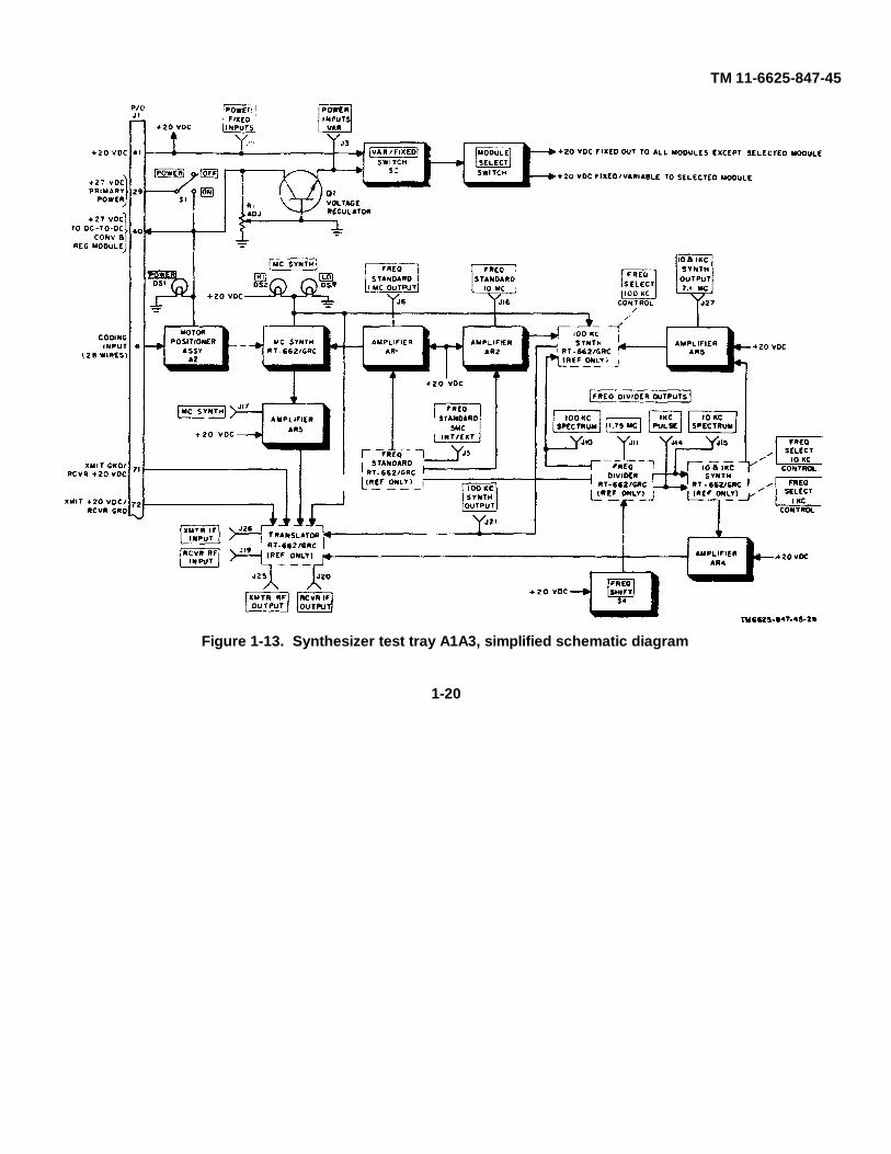
NOTEPrefix reference designators withsynthesizer test tray A1A3 referencedesignator A1A3, unless otherwisespecified.
a. Figure 1-13 shows the controls, test points,connections, and mechanical coupling available on trayA1A3 for testing the mc synthesizer module, thefrequency standard module, the 10 and 1-kilocycle (kc)synthesizer module, the 100-ke synthesizer module, andthe frequency divider module of the RT-662/GRC. Ontray A1A3 the testing of an individual module requiresstimulus inputs from one or more of the other modulesthat are to be tested by the tray.
b. The +27-volt dc primary power input to trayA1A3 is controlled by POWER switch S1. In the ONposition, POWER switch S1 supplies +27-volt dcprimary power to POWER indicator DS1, to pin 3 offrequency standard
Change 2 1-17
TM 11-6625-847-45
Figure 1-12. Common module tray A1A2, simplified schematic diagram.1-18
TM 11-6625-847-45
module connector J7 (fig. 6-10), to the emitter of voltageregulator transistor Q1, and to pin 40 of tray A1A3connector J1, energizing the converter section of the dc-to-dc converter and regulator module on the test set.The + 20 volt dc input to tray A1A3 is connected tocontact terminal 2 (wiper), section B, of MODULESELECT switch S3. The output voltage from thecollector of voltage regulator transistor Q1 is connectedto contact terminal 3 of FIXED/VAR switch 82 and iscontrolled by POWER ADJ resistor RI. FIX/VAR switchS2 selects the voltage to contact terminal 1, section A,of MODULE SELECT switch S3. In the FIXED position,the FIXED/VAR switch supplies the fixed level + 20-voltdc from the test set to the module selected by MODULESELECT switch S3. When S2 is in the VAR position,the voltage output of voltage regulator transistor Q1 issupplied to the module selected by MODULE SELECTswitch SS. The remaining modules of the RT-662/GRCinstalled on tray A1A3 receive the fixed level +20-voltdc from the test set.
Note. The modules of RT-662/GRC that are mountedon tray A1A3 are part of the SM-442A/ GRC.
c. The frequency standard module of the RT-662/GRC provides a 1-mc RF output signal to amplifiermodule AR1 (fig. 1-13), a 10-mc RF output signal toamplifier module AR2, and a 500-kc RF output signal tothe frequency divider module. The amplified RF out qfamplifier AR1 is the 1-mc input to the mc synthesizermodule. Motor positioner A2 positions the mc shaftcoupler of the mcsynthesizer module to the positionrepresentative of the frequency selected by the MCFREQ controls on the test set. The mc synthesizermodule also provides a high-lo frequency band signal tothe 100-kc synthesizer module and to the translatormodule. The high lo signal controls the switching of thefrequency bands on these modules. MC SYNTH HI/ LOindicators DS2 and DS3 (fig.-10) provide visualindication of the frequency band selected by the mcsynthesizer module. The amplified RF output ofamplifier AR2 is the 10 mc input to the 100-kcsynthesizer module. The 500-kc input to the frequency
divider module provides the 1-kc pulse output and the10-kc spectrum output as inputs to the 10 and 1-kcsynthesizer module and a 100-kc spectrum input to the100-kc synthesizer module. FREQ SHIFT switch S4 isused to check the crystal oscillators on the frequencydivider module. The 10-kc and 1-kc shaft couplers forthe 10 and 1-kc synthesizer module are controlled bythe FREQ SELECT 10 KC and 1 KC controls. The 7.1-mc output of the 10 and 1-kc synthesizer module isamplified by amplifier assembly AR5 and supplied to the100 kc synthesizer module. The output of the 100 kcsynthesizer module is one of the inputs to the translatormodule. The output of the 10 and 1-kc synthesizermodule is amplified by amplifier assembly AR4 and isone of the inputs to the translator module. The RFoutput signal of the mc synthesizer module is amplifiedby amplifier assembly AR3 and is one of the inputs tothe translator module.
d. The amplified output of the mc synthesizermodule is measured at the MC SYNTH OUTPUTconnector. The 1 MC output of the frequency standardmodule is measured at FREQ STANDARD OUTPUTconnector 1 MC. The amplified 10 MC output of thefrequency standard module is measured at FREQSTANDARD OUTPUT connector 10 MC. The output ofthe 100 kc synthesizer module can be measured at 100KC SNYTH OUTPUT connector. The 7.1-mc output ofthe 10 and 1-kc synthesizer module is measured at the10 & 1 KC SYNTH OUTPUT connector 7.1 MC. Theamplified 10 and 1-kc synthesizer module outputs to thetranslator module are measured at 10 & 1 KC SYNTHOUTPUTS connector 10 & 1 KC. The outputs of thefrequency modules are measured at FREQ DIVIDEROUTPUTS connectors 1.75 MC J11, 10 KCSPECTRUM J15, 1 KC PULSE J14, and 100 KCSPECTRUM J10. The outputs of the translator modulecan be monitored at TRANSLATOR OUTPUTS, RCVRIF and XMTR RF. Translator module inputs can bemonitored at connectors TRANSLATOR INPUTS,RCVR RF and XMTR IF. The 5-mc signal from thefrequency standard module can be monitored at FREQSTANDARD 5 MC EXT/INT connector J5.
1-19
TM 11-6625-847-45
Figure 1-13. Synthesizer test tray A1A3, simplified schematic diagram
1-20
TM 11-6625-847-45
1-22. Synthesizer Test Tray A1A3 ElectronicCircuits(fig. 6-11 and 6-12)
Note. Where partial reference designators areused, prefix with synthesizer test tray A1A3 referencedesignator A1A3, unless otherwise specified
a. Amplifier modules AR1 through AR5 are used toamplify the RF output signals of the RT-662/GRCmodules on tray A1A3. The amplifier module consistsof POWER switch S1, VOLT ADJ control RI, and two-stage transistor amplifier board A1.
b. The RF input to the amplifier module iscontrolled by AMPL ON/OFF switch S1. With S1 in theOFF position, the input at J1 to the amplifier module isconnected directly to output connectors J3 and J2 bypassing the amplifier board. With S1 in the ON position,the rf input signal to the amplifier module is coupled tothe base of first stage transistor A1Q1 by capacitorA1Q2. The amplified output of A1Q1 is sampled by theposition of the wiper arm of VOLT ADJ collector loadresistor R1. The sampled portion of the amplifier signalis the input to the base of second amplifier A1Q2. Theamplifier output of A1Q2 is coupled from the emitter bycapacitor A1C5 through the bandpass filter, consisting ofinductor A1L1 and amplifier A1C6, on amplifier modulesAR1, AR2, AR4, and AR5, to contact terminal 4 ofAMPL ON/OFF switch S1. On amplifier module AR3,inductor A1L1 and capacitor A1C6 are connected in aband reject configuration (fig. 6-12) between the outputof A1Q2 and ground. The ON position, the AMPLON/OFF switch connects the amplified output of A1Q2to output connects 33 and J2.
1-23. Converter and Control Tray A1 A4(fig. 1-14 and fig. 6-18)
Note. Prefix reference designation with converter andcontrol tray A1A4 reference designator A1A4, unlessotherwise specified.
a. Figure 1-14 shows the various controls, indicators,connectors stimulus inputs, resistive loads, and testpoints available on tray A1A4 for testing the inverterassembly, the front panel assembly, and the inputs of
the antenna coupler assembly on the AM-349/GRC-106.b. The + 27-volt dc input to tray A1A4 from
the test set is controlled by POWER switch S1. The ONposition, POWER switch S1 supplies + 27-volt dcprimary power to POWER indicator DS1; to CONTROLTEST indicators A1 through A5, B1 through B5, and C1through C5; to GRID DRIVE control resistors R3 andA1R4; and to pin 40 of connector J1, energizing theconverter section of dc-to-dc converter and regulatormodule AS on the test set.
c. When testing the inverter assembly on the AM-3349/GRC-106, INPUT CURRENT switch S6 permits scurrent measurements of the input +27-volt dc primarypower across test points HI and LO TEST SELECTORswitch S8 controls the selection of test points HI andLOA for voltage measurements of the inverter assemblyat connector J12. Position 1 of TEST SELECTORswitch S8 connects the test points to +27-volt dc primarypower at 10 AMP fuse F1. When switch S8 is inposition 2, the test points are connected to pin 9 of J12for measuring the voltage drop across load resistor R9in the test set. With the switch in position 3, the testpoints measure the voltage drop across resistor A2R1 atpin 6 of J12. Position 4 of the TEST SELECTOR switchconnects the test points to pin 13 of J12 for measuringthe voltage drop across resistors A2R2 and A2R3.With the switch in position 5, the test points connect topin 1 and 2 of J12 for measuring the voltage drop acrossresistor R8 on the test set. EXTERNAL BLOWERswitch S7 in the HI position connects pin 10, connectorJ12, and in the LO position, pin 11, connector J12, toload resistor R9 on the test set.
d. When testing the AM-349/GRC-106 front panelassembly at connector J2, CONTROL TEST indicatorC5 indicates a ground at pin 23 of connector J2.CONTROL TEST indicators A1 through AS indicategrounds at pins 6 through 10 of J2, respectively.CONTROL TEST indictors B1 through B4 indicategrounds at pins 17, 18, 14, and 20 of J2, respectively.CONTROL TEST indicators C2, C3, and C4 indicatevoltages at pins 4, 11, and 12 of connector J2,respectively. PA METER TEST GRID DRIVE controlRS controls the level of the dc voltage to pin 25 ofconnector J2. PA METER TEST ANTENNA LOAD/
1-21
TM 11-6625-847-45TUNE control R1 controls the level of the dc voltage tocontact terminal 2 of LOAD/ ANT. TUNE switch S5. TheANT. LOAD/ ANT. TUNE switch connects to pin 30 of J22when set to ANT. LOAD, or to pin 28 of J2 when set ANT.TUNE. PA METER TEST ALC METER control R2controls the level of the dc voltage to pins A3, 27, and 32of connector J2 (fig. 6-13).
e. Testing the inputs to the antenna couplerassembly at connector J3, AM-3349/GRC, CONTROLTEST RF BAND/50 a /WHIP switch S2 selects the panson connector J3 monitored by CONTROL TEST indicatorsAl through A5, B1, and B2 for the three positions of theswitch, CONTROL TEST ANT. MOTOR CONTROLCODE switch S4 grounds pin 23 of connector J3 when inthe RF BAND position, and pin 12 when in the CAPposition. CONTROL TEST ANT. MOTOR CONTROLMONITOR switch S3 selects the pins of J8 monitored byCONTROL TEST indicators B5 and C1. CONTROLTEST indicator B5 indicates a ground at pin 14 onconnector J3 when S3 is set to CAP. or one at pin 22when S3 is set to RF BAND. CONTROL TEST indicatorC1 indicates voltage at pin 14 on connector J3 when S3 isset to CAP. or voltage at pin 22 when S3 is set to RFBAND.
1-24. Driver, Discriminator, and Antenna CouplerTray A1AS(fig. 1-15 and fig. 6-14)
Note. Prefix reference designators with driver,discriminator, and antenna coupler tray A1A5 refer mcdesignator A1A5, unless specified
a. Figure 1-15 shows the various controls,connectors, indicators, stimulus inputs, and test pointsavailable on tray A1A5 for testing the relay assembly,antenna coupler driver assembly, and discriminatorassembly on the AM-349/GRC-106.
b. The + 27-volt dc input to tray A1A5 (fig. 6-14)from the test set is controlled by POWER switch S1. TheON position of POWER switch S1 supplies + 27-volt dcprimary power to POWER indicator DS1; to contactterminal 4 of DRIVER TEST SELECTOR switch S2; toRELAY indicator 1; and to pin 40 of connector J1,energizing the converter section of the dc-to-dc converterand regulator module A3 on the test set.
c. When testing the driver assembly on the, AM-349/GRC-106, DRIVER TEST SELECTOR switch S2controls the selection of test points HI and LO for voltagemeasurements at connector J3 on the A1AT1 attenuatorassembly. Position 1 of the TEST SELECTOR switchconnects the test points to pin 2, connector A1AT1J3, forac filament voltage. With switch S2 in position 2, the testpoints are connected to pin 1 of A1AT1J3 for + 200-voltdc B + voltage measurements. Position 3 connects thetest points to pin 4 of A1AT1J3 for meter voltagemeasurements across load resistor A2R1. Position 4monitors the + 27 vdc bias input voltage to the drivermodule. Position 5 connects the test points acrossresistor A2R1 to ca the current-resistance (IR) drop whichdetermines driver current. DRIVER BAND S switch A151selects, mechanically, load transformers for testing theoutput of the driver assembly at 3.25 me, 15.5 me, and29.5 mc.
d. For discriminator assembly test DISCRIMINATOR. TEST SELECTOR itch S3 controls theselection of DISCRIMINATOR test points HI andLO for voltage measurements of the discriminatorassembly at connector J3. Position 1 of the switch S3connects the test points across connector J8, pins 7 and1; position 2 connects the test points across connector J3,pins 8 and 2; position 3 measures the signal at pin 10 ofconnector TS.
e. When testing the RELAY assembly connected toconnector J10, RELAY CONTROL switch S4 suppliesground to pi 5, 9, 2, and 11 of connector J10, in position2, 3, 4, and 5, respectively. Position I is open. RELAYIndicator 1 indicates + 27-volt &at pin 6 of J10; RELAYindicators 2 through 6 indicate, ground at pins 7, 8, 4, 1,and 8, respectively; RELAY indicator 7 ground at pin 12J10.
f. The antenna coupler test at connector J11 usesANTENNA COUPLER CODE switch S5 for the simulationof coding information to the pins of connector J11selected by the ANTENNA COUPLER 50 Ω DUMMYLOAD/COUPLER TERMINATION WHIP/50 Ω DOUBLETswitch S6. ANTENNA COUPLER CAP. MOTORindicator DS3 indicates a ground at pin 12 and + 27-voltdc at pin 14 of J11. ANTENNA (COUPLER BAND SWMOTOR indicator DS4 indicates a ground at pin 22 and +27-volt dc at pin 28 of connector J11.
1-22
TM 11-6625-847-45
Figure 1-14. Converter and control tray A1A4, simplified schematic diagram.
1-23
TM 11-6625-847-45
Figure 1-15. Driver, discriminator and antenna coupler tray A1A5, simplified diagram.
1-24
TM 11-6625-847-45
Section IV. FUNCTIONAL OPERATION OF MECHANICAL ASSEMBLIES
1-25. General
Paragraphs 1-26 through 1-28 discuss the Technicalassemblies located on tray A1A1, tray A1A3, and trayA1A5 of the SM-442A/ GRC.
1-26. Common Module Tray A1A1(fig. 1-11, fig. 1-16, fig. 3-17(1), and fig. 6-7)
a. The operation of the mechanical modulecouplers on tray A1A1 are controlled by the RF AMPL100 KC SELECTOR knobs on the top panel of the tray.The rotation of the knobs is transferred to theappropriate coupler by sprocket gears on the shafts ofthe selector knob and coupler, connected by a loopdrive chain. An adjustable idler sprocket gear betweentwo sprocket gears is used to adjust the slack from thedrive chain.
b. The gear drive assembly provides themechanical means of position the RF AMPL mc coupleron the RF amplifier module of the RT-662/GRC whenconnected to tray A1A1. The frequency codinginformation input to drive assembly A1 for positioningthe mc coupler is received as a ground on one of the 28input lines as selected by the MC FREQ 10 MC and 1MC frequency selector switches on the test set. Thegear drive assembly is an open circuit seeking assemblythat consists of switch A1S1, relay A1K1, motor A1B1,and associated gearing and mechanical couplers.
Note. Where only partial reference designation areused, prefix with comma module tray A1A1 referencedesignator A1A1, unless otherwise specified.
c. Refer to figures 1-16 and 6-7 in the followingdiscussion. Switch A1S1 is a 28-position rotary switchpositioned by the shaft of motor A1B1. A ground on oneof the contact terminals of switch A1S1 will energizerelay A1K1 if the shaft of motor A1B1 is not at a positionthat is representative of the frequency selected on thetest set. Relay A1K1, when energized, supplies +27-voltdc to energize motor A1B1. motor A1B1 will then rotateand reposition the mc shaft coupler and connectingswitch A1S1 until an open circuit is reached. Upon
reaching an open circuit, switch A1S1 will deenergizerelay A1Kl, removing the + 27-volt dc from motor A1B1.The mc shaft coupler will then be at a position that isrepresentative of the frequency selected.
1-27. Synthesizer Test Tray A1A3(fig. 1-13 and fig. 6-10)
a. Motor drive assembly A2 provides themechanical means of positioning the mc synthesizermodule (on the RT-662/GRC) shaft coupler. Thefrequency coding information input to motor driveassembly A2, for position the mc coupler, is received asa ground on one of the 28 input lines as selected by theMC FREQ 10 MC and 1 MC frequency selector switcheson the test set. The motor drive assembly is an open-circuit seeking assembly that consists of switch A2S1,relay A2K1, motor A2B1, and associated gearing andmechanical couplers.
Note. Where partial reference designators areused, prefix with synthesizer test tray A1A3 referencedesignator A1A3, unless otherwise specified
b. Refer to figure 6-10. and figure 6-14 during thefollowing discussion. Switch A2S1 is a 28 positionrotary switch positioned by the shaft of motor A2B1. Aground on one of the contact terminals of switch A2S1will energize relay A2K1 if the shaft of motor A2B1 is notat a position that is representative of the frequencyselected on the test set. Relay A2K1, when energized,supplies +27-volt dc to energize motor A2B1. MotorA2B1 will then rotate and reposition the mc shaft couplerand switch A2S1 until an open circuit is reached. Uponreaching a open circuit, switch A2S1 will deenergizerelay A2K1, removing the +27-volt dc from motor A2B1.The mc shaft coupler will then be at a position that isrepresentative of the frequency selected.
1-28. Driver, Discriminator, and Antenna Coupler Tray A1A5(fig. 1-15 and fig. 6-14)
The operation of turret assembly A1A1 is controlled bythe DRIVER BAND SEL switch on the top panel of trayA1A5. The BAND
1-25
TM 11-6625-847-45
Figure 1-16. Gear drive assembly functional block diagram
SEL control is connected to the turret assembly by aloop drive -chain connected to sprocket gears on the
shafts of the turret assembly and the BAND SEL control.Rotating the BAND SEL control positions the turretassembly to one of three detented positions, 8.25 MC,15.5 MC, and 29.5 MC, representing the low, middle,and high ends of the frequency band o the driverassembly on the AM-3349/GRC2 106. TransformersT1, T2, and T3, mounted on the turret assembly,provide the proper impedance loads for the driverassembly (when mounted on tray A1A5) for thefrequencies selected. The wiper contacts on theappropriate transformer mesh with the contacts on thedriver assembly when the turret assembly is In adetonate position. When the turret assembly is not in adetonate position (rotating), microswitch A1S1disconnects the + 200-volt dc B + supply voltage fromthe driver assembly and extinguishes 200 VDC indicatorDS2.
Figure 1-17. Test set pulse generator assembly block diagram.
1-26
TM 11-6625-847-45
Figure 1-18. Test Set dc-to-dc converter and regulator module A3, block diagram
Figure 1-19. Test set IF oscillator section, block diagram
CHANGE 1 1-27
TM 11-6625-847-45
CHAPTER 2
TROUBLESHOOTING
Section I. GENERAL TROUBLESHOOTING TECHNIQUES
Warnings:1. Voltages as high as 200 volts dc and 115 volts
ac exist in the SM-442A/GRC. Be extremely carefulwhen working on the equipment when it is out of itscase.
2. Operation and maintenance personnel shouldbe familiar with the requirements of TB SIG 291before attempting installation, operation, or repair ofthe SM-442A/GRC.
2-1. General Instructions
Troubleshooting at the GS and depot maintenancecategories includes all the techniques outlined fororganizational maintenance and any special or additionaltechniques required to isolate a malfunction to a specificfunctional circuit or stage and then to locate the defectivepart or parts. Section II, (paras 2-18 through 2-23)provides intraunit (within the unit) troubleshootingprocedures to be used by the GS category maintenancepersonnel in localizing and isolating circuit malfunctionswithin the modules and subassemblies of the SM-442A/GRC.
2-2. Organization of Troubleshooting Procedure
a. General. The first procedure in servicing themodules and subassemblies of the SM-442A/GRC is tosectionalize the fault, which means tracing the fault to afunctional circuit such as the regulator circuitry in dc-to dcconverter and regulator module A3 of the test set. thesecond procedure is to localize the fault by tracing the
trouble to a stage within a defective functional circuit.The third and final procedure is to isolate the trouble to adefective part or parts responsible for the fault. Somedefective parts, such as burned resistors and arcing,shorted transformers can often be located by sight, smell,and hearing. Most defective parts, however, must beisolated by checking voltages and resistances.
b. Sectionalization. The SM-442A/GRC consists offive test trays which are used, independent of each other,with the test set. The first procedure in tracing the troublein the module or subassembly is to locate the functionalcircuit at fault by the following methods:
(1) Visual inspection. The purpose of visualinspection is to locate faults without testing ormeasuring circuits.All meter indications or other visual signs shouldbe observed and an attempt made to sectionalizethe trouble to a functional circuit within themodule or subassembly being tested at the time.
(2) Operational tests. Operational tests frequentlyindicate the general location of the trouble. Inmany instances the tests will help in determiningthe exact nature of the fault. The operationalperformance given in paragraphs 4-1 through 4-12 for the individual modules and assemblies ofthe SM-442A/GRC can be used to sectionalizethe trouble to a particular functional circuit.
c. Localization. Localization procedures should beperformed after the trouble has been sectionalized (babove). The localization procedures
2-1
TM 11-6625-847-45
applicable to this equipment are listed in (1) and (2) belowand should be used to localize the trouble to a stagewithin a defective functional circuit.
(1) Troubleshooting chart. The troubleshootingcharts, paragraphs 2-18 through 2-23, listthe symptoms of common troublesoccurring within the modules and,subassemblies of the SM-442A/GRC andgive (or references) corrective measures.The troubleshooting chart are to be used inconjunction with the performance testsgiven in paragraphs 4-1 through 4-12 asdescribed in paragraph 2-4. The charts donot list all the troubles that may occur. Therepairman should use these charts as aguide in analyzing symptoms that are notlisted.
(2) Stage gain charts. The stage gain charts(paras 2-14 and 2-16) will help in locatingdifficult troubles that produce weak signalsin amplifier modules AR1 through AR5 andIF amplifier module Al.
(3) Wave shapes. When troubleshooting thepulse generator module, compare the waveshapes in figure 1-17 with those obtainedusing the procedures in paragraph 2-10 andtroubleshooting chart 2-19
d. Isolate Once the trouble has been localized to aparticular stage of a functional circuit, the faultycomponents responsible for the malfunction can beisolated by applying one or more of the followingprocedures:
(1) Voltage measure. Th is equipment istransistorized. When making voltagemeasurements, use the same voltmeterspecified ill the troubleshooting charts andthe schematic diagrams of the modules andsubassemblies. Use tape or sleeving(spaghetti) to insulate the entire test prod,
except for the extreme tip.
(2) Resistance measurements .Makeresistance measurements only as directedin the troubleshooting charts and schematicdiagrams and in paragraph 2-17.
CAUTION: Before using any ohmmeterto test transistors or transistor circuits,check the open-circuit voltage acrossthe ohmmeter test leads Do not use anohmmeter or a multimeter it the open-circuit voltage exceeds 1.5 volts.Since the Rx1 range normallyconnects the ohmmeter internalbattery directly across the test leads,the comparatively high current (50 maor more) may damage the transistorunder test. The Rx1 range of anyohmmeter should not be used whentesting low-powered transistor
(3) Intermittent troubles. In all tests, thepossibility of intermittent troubles should notbe overlooked. If present, this type oftrouble often may be made to appear bytapping or jarring the equipment. Make avisual inspection of the wiring andconnections to the units of the SM-442A/GRC. Minute cracks in printed circuitboards can cause intermittent operational Amagnifying glass is helpful in locatingdefects in printed boards. Continuitymeasurements of printed conductors maybe made using the same techniquesordinarily used on hidden conventionalwiring; follow the ohmmeter precautions in(2) above
2-3. Test Equipment
The chart below lists the test equipment required fortroubleshooting the SM-442A/GRC.
Test equipment Technical manual Federal stock No.
Multimeter AN/PSM-6B TM 11-6625-475-10 6625-643-1686Voltmeter, Electronic AN TM 11-6625-475-10 6625-973-3986
URM-1452-2
TM 11-6625-847-45
Test equipment Technical manual Federal stock No.Analyzer, Spectrum TS-723(*)/ TM 11-5097 6625-668-9418U*Frequency Selective Voltmeter None None(equivalent to be selected).Generator, Signal AN/URM- TM 11-6625-683-15 6675-783-5965
427.Oscilloscope AN/USM-140(*)b TM11-6625-535-15 and 6625-066-2525
TM 11-4625-535-15-1.Generator, Signal AN/URM- TM 11-625-573-15 662-868-8353
50.Multimeter ME-26(*)/Uc TM 11-6625-200-12 6625-360-2493Power Supply PP-3940/G ---------- TM 11-6130-247-15 6130-985-8136Tee Connector UG-274B/U ---------- None 5935-702-0125Test Cables W15, W1, W2,
W3, W22, and W25.Charger, Battery PP-1451/G -------- TM 11-6130-236-12 6130-985-8157Electronic Counter, Digital TM 11-6625-700-10 6625-911-6368
Readout, AN/USM-207.
aAnalyzer, Spectrum TS-723(*)/U represents Analyzer, Spectrurn TS-733A/U, TS-723B/U, or TS-732C/U, or TS-723D/U.bOscilloscope AN/USM-140(*) represents Oscilloscope AN/USM-140A or AN/USM-140B.cMultimeter MS-26(*)/U represents Multimeter ME-26A/U, ME-26B/U, ME-26C/U. or ME-26D/U.
Cautions:
1. Test set A2 contains transistor circuits. Neverconnect the 2 types of test equipments which haveoutputs directly to transistor circuits; use couplingcapacitors. Some of the modules have input and outputcoupling capacitors in their circuitry; check the schematicdiagram of the respective modular assembly.
2. Make test equipment connections with care sothat short circuits will not be caused by exposed testequipment connectors. Tape or use sleeves (spaghetti)on test prods or clips as necessary to leave as little areaexposed as needed to make contact to the circuit undertest.
3. The test set is recommended as a source ofpower (para. 2-5) when servicing the transistorizedmodules and subassemblies. Observe the polarity of thepower source. Polarity reversal may damage thetransistors or electrolytic capacitors in the circuit. If apower -source other than the one contained in the test 9 isused, it must have good voltage regulator and low acripple. Good regulation is important because the outputvoltage of a power supply that has poor regulation mayexceed i maximum voltage rating of the transistors themodule or subassembly being tested.
2-4. Use of Troubleshooting Charts
Troubleshooting the SM-442A/GRC is based on thetrouble localization and trouble isolation charts given inTM 11-6625-847-12 and the troubleshooting charts inparagraphs 2-18 through 2-23 of this manual. Duringtroubleshooting, if trouble within the SM-442A is isolatedto a module or assembly, perform or apply the correctivemeasures given in the chart. Refer to paragraph 2-17 forthe proper technique in isolating defective parts within astage. The troubleshooting charts given in TM 11-6625-847-12 are suitable for isolating SM-442A/GRCmalfunctions of controls, switches, indicating lamps,modules, and subassemblies; however, they are not to beused to locate troubles within a defective module orsubassembly. If organizational maintenance has notisolated a trouble to a control, switch, module, orsubassembly, general support maintenance will starttroubleshooting by using the troubleshooting checks in TM11-6625-847-12 and performing the corrective actionscited.
2-5. Power Supply Requirements
Testing the various modules and subassemblies of theSM-442A/GRC requires connection to a power source of+ 20-3 -, and + 27 volt dc, depending on the powerrequirements of the module or subassembly being tested.If
Change 1 2-3

TM 11-6625-847-45
standard dc power supplies are not available, the + 20-volt dc supply voltage can be obtained from the frontpanel of the test set at DC VOLTAGE test points +20 andground, and the -33 volt dc supply voltage from acrosstest points RCVR IF HI and LO on tray A1A2, connectedto the test set and energized, with the RCVR IF TESTSELECTOR switch set to position 1. The dc voltagerequired by the SM-442A/GRC is supplied by a 27-volt dcpower source, connected to the POWER connector on thetest. A typical power source for the set is given inparagraph 2-3. It has a voltage range of 20 .to 32 volts dcand a direct current range of 100 amperes, maximum.
2-6. General Troubleshooting Information
Information on the function and operation of test set andtest tray controls, switches, and lamps is contained in TM11-6625-847-12. Instructions for removal andreplacement of modules, board assemblies, andcomponent parts are given in paragraphs 3-1 through 3-54. When replacing any defective wiring or componentparts, refer to the wiring and soldering instructions innotes, paragraph 3-12.
2-7. Troubleshooting Test Set Dc-to-DcConverter and Regulator Module A3
When troubleshooting dc-to-dc converter and regulatormodule A3, perform the general support tests given inparagraph 4-6. Refer to figure 1-18 and thetroubleshooting chart in paragraph 2-18 for localizing andisolating malfunctions.
2-8. Troubleshooting Test Set Dc-to-Dc ConverterModule A2
Dc-to-dc converter module A2 is an encapsulated unitwhich is not repairable. To troubleshoot the module,perform the general support tests given in paragraph 4-5.Replace module A2 if any of the performance standardsare not satisfied.
2-9. Troubleshooting Test Set Pulse GeneratorModule A1A1
When troubleshooting the pulse generator module,perform the general support tests given in paragraph 4-7.
Refer to figure 6-4 and troubleshooting chart 2-19 forlocalizing. and isolating malfunctions. When checkingpulse wave forms in pulse generator module A1A1,connect the test equipment as described in paragraph 2-10.
2-10. Test Set Pulse Generator Module A1A1Waveform Check
Connect Tee Connector UG-274B/U to the output ofGenerator, Signal AN/URM-127. Connect one side ofUG-274B/U to connector J1 on pulse generator assemblyA1A1 and the other side to the trigger input onOscilloscope AN/USM-140(*). Connect 20 volts dcbetween terminals 3 and 4 (ground) and -30 volts dcbetween terminals 14 and 4 (ground), using the test set asa power source (para. 2-5). Adjust the output of theAN/URM-127 to 500 cycles per second (cps) at 2 voltspeak to peak. Connect the AN/USM-140(*) probe asdirected in troubleshooting chart 2-19, and compare thewaveforms obtained with those illustrated in figure 1-17.
2-11. Troubleshooting Test Set If. Oscillator ModulesA1A2, A1A3, and A1A4
When troubleshooting any of the oscillator modules,perform the general support tests in paragraph 4-8. Referto figure 1-19, figure 6-3 and figure 6-6 and thetroubleshooting chart (para. 2-20) for localizing andisolating malfunctions. The only difference in the circuitryof the oscillator modules is the operating frequency of thecrystal used in each module. When signal tracing in anyof the oscillator modules, use the test set as a source ofpower and the AN/USM-140(*) with a probe having dcisolation. Make sure that one side of AN/USM-140(*) isgrounded; connect the probe as directed in thetroubleshooting chart (para. 2-20).
2-12. Troubleshooting Test Set Mixer Module A1A5
When troubleshooting mixer module A1A1, perform thegeneral support tests in paragraph 4-9. Refer to figure 6-3 and the troubleshooting chart in paragraph 2-21 forlocalizing a isolating malfunctions.
Change 1 2-4
TM 11-6625-847-45
1-13. Troubleshooting Common Module ray A1A2 If.Amplifier Module A1
When troubleshooting amplifier module A1, perform thegeneral support tests in paragraph 4-10. Refer to figure69 and the troubleshooting chart in paragraph 2-22 forlocalizing and isolating malfunctions. When the output ofthe if. amplifier module is abnormally low or distorted,make the stage gain measurement as indicated inparagraph 2-14 to localize the fault.
2-14. Stage Gain Measurements (IF Amplifier Module A1)
Connect test equipment to IF amplifier module as shownin figure 6-20. If a 20-volt dc power supply is notavailable, use the +20 volt dc output of the test set asdescribed in paragraph 2-5.
a. Gain Measurements. Adjust the output ofGenerator, Signal AN/GRM-50 to 1 ± 0.2 millivolts (mv) at1.75 megacycles. Connect a Multimeter ME-26(*)/Ubetween terminal E5 and ground, and adjust 10-kilohm
potentiometer A2R5 for an indication of + 1.5 volts.Leave the AN/GRM-50 connected between terminals E2and E3 throughout test. Disconnect the ME-26(*)/U fromterminal E5, and connect Voltmeter, Electronic AN/URM-145 as directed in the stage gain chart (b below).Comparethe indications on the AN/URM-145 with those listed in theOutput of stage column. Agreement within 10 percentindicates normal operation. Stage gain is computed bydividing the output voltage of the transistor stage undertest by the input voltage to the transistor stage. Thecumulative gain in decibels of the if. amplifier iscomputed by applying the following formula:
Gain in db = 20 Log E1/E2
E1 is the output voltage, and E2 is the input voltage to theif. amplifier module. Since the output voltage is 9.6 mvfor an input of 1 mv, the cumulative gain in db is 20 Log9.6 mv (20 x .9823) which equals 19.65. This result iswithin the design specifications of the if. amplifier module(gain of 20 ±0.5 db).
b. Stage Gain Chart.
Test connections Voltage (mv) Stage gainAN/GRM-50 AN/U RM-145 Input to Output
stage of stage
Between E2 and E3 (ground) - Collector of Q3 1 3.2 3.2Same as above Collector J3 (Q6) 3.2 9.6 8
2-15. Troubleshooting Synthesizer Test Tray A1A3 (Amplifier Modules AR1 through AR5)
When troubleshooting amplifier modules AR1 throughAR5, perform the general support tests in paragraphs 4-11 and 4-12. Refer to figure 6-11 and 6-12 and theshooting chart in paragraph 2-28 for localizing andisolating malfunctions. If any of the outputs f amplifiermodules AR1 through AR5 is abnormally low or distortedmake the stage gain measurements in paragraph 2-16 tohelp localize the fault.
2-16. Stage Gain Measurements, Tray A1A3 (AmplifierModules All Through AR5)
Connect the test equipment to the amplifier module undertest as shown in figure 6-21. If a 20-volt dc power supplyIs not available, use the 20-volt dc output of the test setas described in paragraph 2-5.
a. Gain Measurement. Adjust the output of theAN/GRM-50 to 50 mv at 1 megacycle and rotatepotentiometer R1 fully connected the AN/URM-145 eadirected in the stage gain chart (b below). Compare theindication
2-5
TM 11-6625-847-45
obtained on the AN/URM-145 with those listed in theoutput column. Agreement within 10 percent indicateswithin normal operations. Stage gains computed by
dividing the output voyage of the transistor stage undertest by the input voltage to the transistor stages
b. Stage Gain Chart.TEST connection VOLTAGE
AMPLIFIER AN/GRM-50- AN/URM-145 (Mv)module Input to Output of Stage
transistor transistor gainstage stage
AR3 Connector J1 Collector of Q1 50 780 ±10% 15.6 ±10%Connector J1 Connector J3 780 590 ±10% 0.76 ±10%
(Q2)AR1, AR2, Connector J Collector of 50 847± 10% 16.9 ±10%
AR4,and Q1AR5 Connector J1 Connector J3 847 625± 10% 0.74 ±10%
(Q2)
2-17. Isolating Trouble Within Stage
When trouble has been localized to a stage, use thefollowing techniques to isolate the defective part:
a. In-Circuit Transistor Voltage Measurements. Iftransistors are wired in the circuit, troubleshoot theequipment without physically unsoldering and removingtransistors. If transistors can be removed without the useof a soldering iron, test them out of the circuit. If atransistor tester is available, test the pluckout transistorsbefore making other circuit test For in-circuit to , makethe transistor dc voltage measurements indicated on theschematic diagram of the module being tested. Carefullyfollow instruction and observe notes on schematicdiagrams; carelessness may cause more troubles in theequipment and make the troubleshooting job moredifficult. Do not remove or insert a transistor with voltageapplied to the circuit. If the dc voltage at the emitter,collector, or base of the transistor being checked isabnormally low or high, make in-circuit transistorresistance measurements using the techniques describedin b below.
b. In-Circuit Transistor Resistance Measurement.
When measuring the resistance of circuit elementsconnected across the junctions of any transistor (base-emitter or base-collector), consider the polarity of the ME-26(*)/U and try measurements with the ME-26(*)/Uconnected one way; then reverse the leads. For example,figure 6-12 shows a typical common emitter stage (Q1)used in each of the amplifier modules (AR1 through AR5).If the positive lead of the ME-26(*)/U is placed at thejunction of R2 and R3 and the negative lead is placed atground when measuring RS in this circuit, the ME-26(*)/Ubattery forward biases the base-emitter junction, causinga short circuit between the base and emitter. This placesRS in parallel with R4 and R5. The MS 26(*)/U indicationwill be slightly less than 60 ohms because of the parallelresistances. If the ME-26(*)/U leads are then reversed,the transistor will be reverse-biased, causing a very highresistance to appear between the base and the emitter. Inthis case, the indication would be 820 ohms, the value ofR3. If the indication is the same in both case, thetransistor is probably open-circuited or short-circuited.Consider, all, that differ values of resistance will beobtained with the ME-26(*)/U on different ranges. Forexample, if the transistor junction or a resistor plus thetransistor junction is measured in the forward direction orthe RX10 range, the actual indication will be less than iftaken with the ME-26(*)/U ok the RX100 range.
2-6

TM 11-6625-847-45Section II. TROUBLESHOOTING CHARTS
2-18. Troubleshooting Chart, Test Set (Dc-to-Dc Converter and Regulator Module A3)
Note. Attach tray A1A1 to the Test set. Refer to paragraph 2-7 before using chart.
ItemNo. Indication Probable trouble Procedure
1 The + 20 volt dc output Defective series regulating Connect the ME-26 (*)/Ulevel is not indicated transistor 1A1Q1. between test point J11 on trayon the ME-26(*)/U A1A5 and ground. Checkwhen the TEST for an indication of +20SELECTOR switch on volts dc. If +20 volts dc is nottray A1A1 is set to indicated, check transistorposition 2 1A1Q1 in the test set for
defects. Replace defective parts,
2 The + 1 volt dc con- Defective +20-volt dc regulating Se LOAD SELECT switch onverter output does circuit tray A1A1 to 500, and makenot stay within the the voltage measurements inlimits of +19.1 to a through d below using the+19.9 volts (LOAD ME-26 (*)/U.SELECT switch ontray A1A1 set to 100)and +19A to +19.6volts (LOAD SELECTswitch on trayA1A1 set to 500)when the primary dcsource connected tothe test set is adjustedto +27 and+20 volts respectively.
a Connect the ME-26(*)/Ubetween the emitter oftransistor A1Q4 ad grandCheck for an indication of+4.0 volts de. If +4.0volts dc is not Indicated,check resistor A1R6 andtransistors A1QS andA1Q4 for defects. Replacedefective parts.
b. If the ME-26(*)/U indicates+4.0 o dc in aabove, connect the ME-2W(*)/U between the baseof transistor A1QS andground and check for anindication of +4.8 voltsde. If Indication is notapproximately +4.8 voltsde, check Zener diodeA1VR2 and resistorsA1R2 and A1R4 fordefects. Replace defectiveparts.
2-7
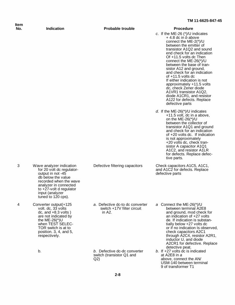
TM 11-6625-847-45ItemNo. Indication Probable trouble Procedure
c. If the ME-26 (*)/U indicates+ 4.8 dc in b aboveconnect the ME-2(*)/Ubetween the emitter oftransistor A1Q2 and soundend check for an indicationOf +11.5 volts dc Thenconnect the ME-26(*)/Ubetween the base of tran-sistor A12 and ground,and check for an indicationof +11.5 volts dcIf either indication is notapproximately +11.5 voltsdc, check Zener diodeA1VR1 transistor A1Q2,diode A1CR1, and resistorA122 for defects. Replacedefective parts
d. If the ME-26(*)/U indicates+11.5 volt, dc in a above,on the ME-26(*)/Ubetween the collector oftransistor A1Q1 and groundand check for an indicationof +20 volts dc. If indicationis not approximately+20 volts dc, check tran-sistor A capacitor A1Q1A1C2, and resistor A1LRfor defects. Replace defec-tive parts.
3 Wave analyzer indication Defective filtering capacitors Check capacitors A1C5, A1C1,for 20 volt dc regulator- and A1C2 for defects. Replaceoutput in not -45 defective partsdb below the valuerecorded when the waveanalyzer in connectedto +27-volt d regulatorinput (analyzertuned to 120 cps).
4 Converter output(+125 a. Defective dc-to dc converter a Connect the ME-26(*)/Uvolt. dc, 33 volts switch +17V filter circuit between terminal A2E8dc, and +8.3 volts ) in A2. and ground, mod check forare not indicated by an indication of +27 voltsthe ME-26(*)U de. If indication is substan-when TEST SELEC- tially below +27 volts dcTOR switch is at to or if no indication Is observed,position. 3, 4, and 5, check capacitors A2C1respectively. through A2C4, resistor A2R1,
inductor U, and diodeA2CR1 for defective. Replacedetective peat.
b. b. Defective dc-dc converter b. If +27 volts dc is indicatedswitch (transistor Q1 and at A2E8 in aQ2) above, connect the AN/
USM-140 between terminal9 of transformer T1
2-8
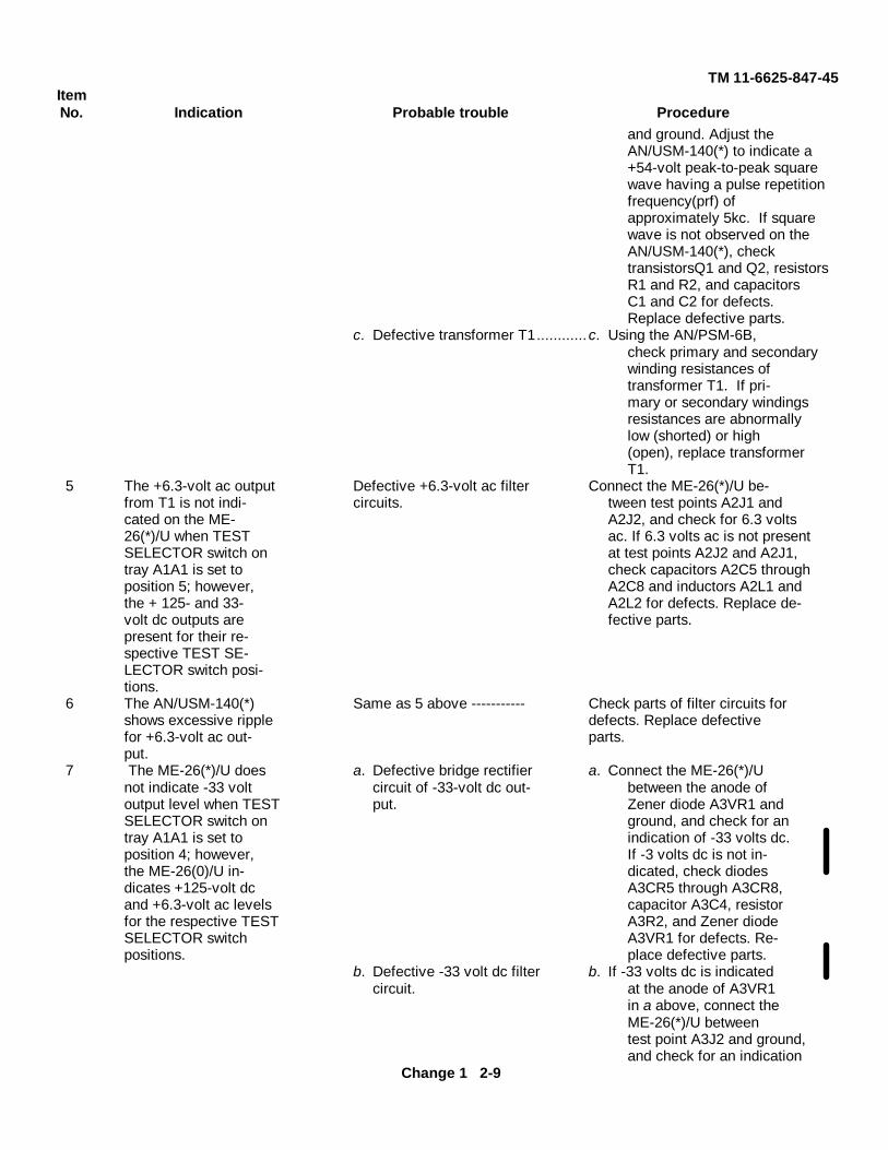
TM 11-6625-847-45ItemNo. Indication Probable trouble Procedure
and ground. Adjust theAN/USM-140(*) to indicate a+54-volt peak-to-peak squarewave having a pulse repetitionfrequency(prf) ofapproximately 5kc. If squarewave is not observed on theAN/USM-140(*), checktransistorsQ1 and Q2, resistorsR1 and R2, and capacitorsC1 and C2 for defects.Replace defective parts.
c. Defective transformer T1............c. Using the AN/PSM-6B,check primary and secondarywinding resistances oftransformer T1. If pri-mary or secondary windingsresistances are abnormallylow (shorted) or high(open), replace transformerT1.
5 The +6.3-volt ac output Defective +6.3-volt ac filter Connect the ME-26(*)/U be-from T1 is not indi- circuits. tween test points A2J1 andcated on the ME- A2J2, and check for 6.3 volts26(*)/U when TEST ac. If 6.3 volts ac is not presentSELECTOR switch on at test points A2J2 and A2J1,tray A1A1 is set to check capacitors A2C5 throughposition 5; however, A2C8 and inductors A2L1 andthe + 125- and 33- A2L2 for defects. Replace de-volt dc outputs are fective parts.present for their re-spective TEST SE-LECTOR switch posi-tions.
6 The AN/USM-140(*) Same as 5 above ----------- Check parts of filter circuits forshows excessive ripple defects. Replace defectivefor +6.3-volt ac out- parts.put.
7 The ME-26(*)/U does a. Defective bridge rectifier a. Connect the ME-26(*)/Unot indicate -33 volt circuit of -33-volt dc out- between the anode ofoutput level when TEST put. Zener diode A3VR1 andSELECTOR switch on ground, and check for antray A1A1 is set to indication of -33 volts dc.position 4; however, If -3 volts dc is not in-the ME-26(0)/U in- dicated, check diodesdicates +125-volt dc A3CR5 through A3CR8,and +6.3-volt ac levels capacitor A3C4, resistorfor the respective TEST A3R2, and Zener diodeSELECTOR switch A3VR1 for defects. Re-positions. place defective parts.
b. Defective -33 volt dc filter b. If -33 volts dc is indicatedcircuit. at the anode of A3VR1
in a above, connect theME-26(*)/U betweentest point A3J2 and ground,and check for an indication
Change 1 2-9
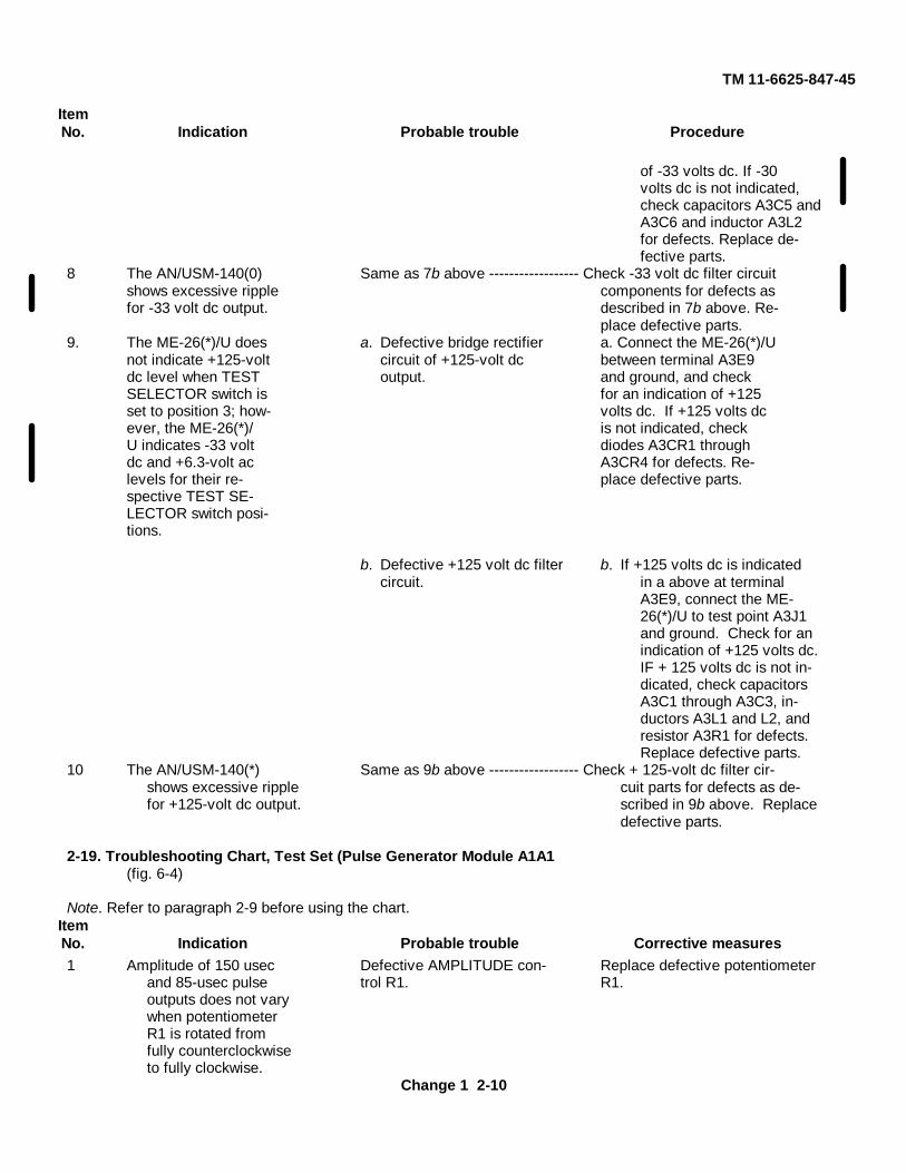
TM 11-6625-847-45
ItemNo. Indication Probable trouble Procedure
of -33 volts dc. If -30volts dc is not indicated,check capacitors A3C5 andA3C6 and inductor A3L2for defects. Replace de-fective parts.
8 The AN/USM-140(0) Same as 7b above ------------------ Check -33 volt dc filter circuitshows excessive ripple components for defects asfor -33 volt dc output. described in 7b above. Re-
place defective parts.9. The ME-26(*)/U does a. Defective bridge rectifier a. Connect the ME-26(*)/U
not indicate +125-volt circuit of +125-volt dc between terminal A3E9dc level when TEST output. and ground, and checkSELECTOR switch is for an indication of +125set to position 3; how- volts dc. If +125 volts dcever, the ME-26(*)/ is not indicated, checkU indicates -33 volt diodes A3CR1 throughdc and +6.3-volt ac A3CR4 for defects. Re-levels for their re- place defective parts.spective TEST SE-LECTOR switch posi-tions.
b. Defective +125 volt dc filter b. If +125 volts dc is indicatedcircuit. in a above at terminal
A3E9, connect the ME-26(*)/U to test point A3J1and ground. Check for anindication of +125 volts dc.IF + 125 volts dc is not in-dicated, check capacitorsA3C1 through A3C3, in-ductors A3L1 and L2, andresistor A3R1 for defects.Replace defective parts.
10 The AN/USM-140(*) Same as 9b above ------------------ Check + 125-volt dc filter cir-shows excessive ripple cuit parts for defects as de-for +125-volt dc output. scribed in 9b above. Replace
defective parts.
2-19. Troubleshooting Chart, Test Set (Pulse Generator Module A1A1(fig. 6-4)
Note. Refer to paragraph 2-9 before using the chart.ItemNo. Indication Probable trouble Corrective measures1 Amplitude of 150 usec Defective AMPLITUDE con- Replace defective potentiometer
and 85-usec pulse trol R1. R1.outputs does not varywhen potentiometerR1 is rotated fromfully counterclockwiseto fully clockwise.
Change 1 2-10
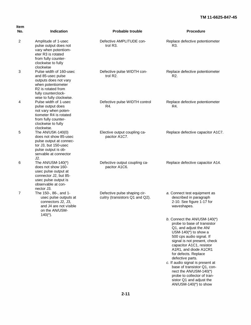
TM 11-6625-847-45
ItemNo. Indication Probable trouble Procedure
2 Amplitude of 1-usec Defective AMPLITUDE con- Replace defective potentiometerpulse output does not trol R3. R3.vary when potentiom-eter R3 is rotatedfrom fully counter-clockwise to fullyclockwise
3 Pulse width of 160-usec Defective pulse WIDTH con- Replace defective potentiometerand 85-usec pulse trol R2. R2.outputs does not varywhen potentiometerR2 is rotated fromfully counterclock-wise to fully clockwise.
4 Pulse width of 1-usec Defective pulse WIDTH control Replace defective potentiometerpulse output does R4. R4.not vary when poten-tiometer R4 is rotatedfrom fully counter-clockwise to fullyclockwise.
5 The AN/USK-140(0) Elective output coupling ca- Replace defective capacitor A1C7.does not show 85-usec pacitor A1C7.pulse output at connec-tor J3, but 150-usecpulse output is ob-servable at connectorJ2.
6 The AN/USM-140(*) Defective output coupling ca- Replace defective capacitor A14.does not show 160- pacitor A1C6.usec pulse output atconnector J2, but 85-usec pulse output isobservable at con-nector J3.
7 The 150-, 86-, and 1- Defective pulse shaping cir- a. Connect test equipment asusec pulse outputs at cuitry (transistors Q1 and Q2). described in paragraphconnectors J2, J3, 2-10. See figure 1-17 forand J4 are not visible waveshapes.on the AN/USM-140(*).
b. Connect the AN/USM-140(*)probe to base of transistorQ1, and adjust the AN/USM-140(*) to show a500 cps audio signal. Ifsignal is not present, checkcapacitor A1C1, resistorA1R1, and diode A1CR1for defects. Replacedefective parts.
c. If audio signal is present atbase of transistor Q1, con-nect the AN/USM-140(*)probe to collector of tran-sistor Q1 and adjust theAN/USM-140(*) to show
2-11
TM 11-6625-847-45ItemNo. Indication Probable trouble Procedure
a 600-cps square wave.If square wave in not pres-ent, check transistor Q1for defects. Replace de-fective parts.
d. If square wave Is present atcollector of transistor Q1,connect the AN/USM-140(*) probe to collectorof transistor Q2 and ob-serve 500-cps square wave.If square wave is not present, check transistor Q2,capacitor A1C2 and resis-tors A1R2 and A1R3 fordefects. Replace defectiveparts.
8 The 1-usee pulse out- a. Defective pulse shaping and a. Perform the following:put is not shown on amplifier circuit (transistor (1) Connect test equip-the AN/USM-140(*) Q6). ment as described inat connector J4; how- paragraph 2-10.ever, 150-usec and (2) Connect the AN/USM-85-usec pulse outputs 140(*) probe toare observable at con- collector of transis-nectors J2 and J3. tor Q8, and adjust
the AN/USM-140(*)to observe a 500-cps square wave. Ifsquare wave is notpresent, check tran-sistor Q6, capacitorC8, and resistorsA1R16 and A1R17for defects. Replacedefective parts.
b. Defective differentiating and b. If 500-cps square wave issquaring circuit. present at collector of tran-
sistor Q6, connect theAN/USM-140(*) probe tobase of transistor Q7 andadjust the AN/USM-140(*) show 500-cps posi-tive trigger pulse. If trigger pulses are not present,check diodes A1CR4 andA1CR5, resistor A1R18,and capacitor A1C9 fordefect. Replace defectiveparts.
c. Defective 8chmitt trigger c. If positive trigger pulses aremultivibrator (transistors present at base of transistorQ8 and Q7). Q7, connect the AN/USM-
140(*) probe to collectorof transistor Q8 and ad-just the AN/USM-140(*)to show 1-usec wide posi-tive pulses (control R3rotated fully clockwise).
2-12
TM 11-6625-847-45
ItemNo. Indication Probable trouble Procedure
If positive 1-use pulsesare not present, check tran-sistors Q7 and Q8, capaci-tors A1C10 and A1C11,and resistors A1R19, ARW20A1R21, and A1R22 fordefects. Replace defectiveparts.
d. Defective output coupling d. Replace defective capacitorcapacitor A1C12. A1C12.
9 The 150-usec and 85- a. Defective squaring circuit. a. Perform the following:usec pulse outputs (1) Connect test equip-are not observable on ment as described inthe AN/USM-140(*) paragraph 2-10.at connectors J2 and (2) Connect the AN/USM-J3; however, 1-usec 140(*) probe topulse output is ob- collector of transis-servable at connector tor Q3, and adjustJ4. the AN/USM-
140(*) to show 500-cps positive triggerpulses. If triggerpulses are not pres-ent, check diodesA1CR2 and A1CR3,resistors A14,A1R6 and A1R6,and capacitor A1C3for defects. Replacedefective parts.
b. Defective monostable multi- b. If positive trigger pulsesvibrator (transistors Q3 are present at collector ofand Q4). transistor Q4 in a above,
connect the AN/USM-140(*)probe to collector of tran-sistor Q4 and adjust theAN/U8M-140(*) to show150-usec wide positive pulses(control R2 rotated fullyclockwise). If 150-usecpulses are not present,check transistors Q3 andQ4, capacitors A1C4 andA1C5, and resistors A1R8through A1R12 for defects.Replace defective parts.
c. Defective output amplifier c. If positive pulses are present atcircuit (transistor Q3). collector of transistor Q4 in
b above, connect the AN/USM-140(*) probe toemitter of transistor Q5and adjust the AN/USM-140(*) to show 150-usecnegative pulses. If nega-tive pulses are not present,check transistor Q5, resis-tors A1R15 and A1R14, and
2-13
TM 11-6625-847-45ItemNo. Indication Probable trouble Procedure
output coupling capacitorsA1C6 and A1C7 for defects.Replace defective parts.
2-20. Troubleshooting Chart, Test Set (IF Oscillators A1A2, A1A3, and A1A4)(figs. 1-19, 6-3, and 6-6)
Note. Refer to paragraph 2-11 before using the chart.
ItemNo. Indication Probable trouble Procedure
1 The AN/USM-140(*) Defective potentiometer control With no power or signal inputsoutput level indication R1. connected to the oscillatoror the AN/URM- assembly, connect the AN/145 does not vary when PSM-6B between. terminal 5potentiometer con- and ground. Rotate the po-trol R1 in varied from tentiometer from fully coun-fully counterclock- terclockwise to fully clock-wise to fully clock- wise, and check the AN/PSM-wise. 6B for a resistance variation
from 0 to 250 ohms. Replacepotentiometer R1 if defec-tive
2 Electronic Counter, Defective crystal Y1 or capaci- Replace crystal Y1 or capacitorsDigital Readout. AN/ tors C1 and C2 in A1. C1 and C2 in A1, if defective.USM-207 does notindicate the correctfrequency for the oscil-lator under test.
3 Frequency indication on Defective variable capacitor A1C1. Replace variable capacitor A1C1.the AN/USM-207does not vary whenvariable capacitor C1is rotated through itsfull travel.
4 Oscillator output level a. Defective crystal tank cir- a. Perform the following:from A1 is not indi- cuit. (1) Connect test equip-ted on the AN/URM- ment as described145 with potentiometer in paragraph 2-11.R1 adjusted fully (2) Adjust the AN/USM-clockwise. 140(*) to show a
1.75mc signal.(3) Connect the AN/USM-
140(*) probe tobase of transistorQ1 (turn gain con-trol up on the AN/USM-140(*) andcheck for a 1.75-mcsinusoidal signal.if signal is not pres-ent, cheek crystalY1 and on A1 (fig.6-3), diodes CR1and CR2, resistorsR2, R4, and RT1,and capacitors C1
2-14

TM 11-6625-847-45
ItemNo. Indication Probable trouble Procedure
through C4 for de-fects. Replace de-fective parts (fig.6-6).
b. Defective oscillator stage b. If a 1.75-mc signal is presentQ1. at base of transistor Q1 in
a above, connect the AN/USM-140(*) probe to thecollector of transistor Q1and adjust the AN/USM-140(*) to show a 1.76-mcsignal. If signal is not pre-ent, check translator Q1,resistors R7, RB, and R10,and capacitors C5, C6, andC8 for defects. Replacedefective parts.
c. Defective buffer amplifier c. If 1.75-mc signal is presentstage Q2. in b above at collector of
transistor Q1, connect theAN/USM-140(*) probe toemitter of transistor Q2and adjust the AN/USM-140(*) to show a 1.76-mc signal. If signal is notpresent, check transistorQ2 and potentiometer R1for defects. Replace de-fective parts.
d. Defective output coupling d. Replace defective capacitorcapacitor C9. C9.
2-21. Troubleshooting Chart, Test Set (Mixer Module A1A5)(fig. 6-3)
Note. Refer to paragraph 2-12 before using chart.ItemNo. Indication Probable trouble Procedure1. When the AN/GRM- Defective potentiometer control With no power or signal inputs
50 is connected to con- R1. to the mixer assembly, connectnector J1, J2, J8, or the AN/PSM-6B betweenJ4, the mixer output connector J2 and ground.at connector J6 does Check the AN/PSM-6B fornot vary an potentiom- resistance indication of 0 toeter R1 is varied 1,000 ohms as potentiometerfrom fully counter- R1 is varied from fully coun-clockwise to fully terclockwise to fully clock-clockwise. wise. If the AN/PSM-6B
does not indicate a variableresistance, replace potentiom-eter R1.
2 When the AN/GRM- a. Defective two-tone mixer a. Perform the following:50 is connected to circuit (diode CR2 and (1) With no power orconnector J1, the fre- associated parts). signal inputs to thequency selective volt- mixer assembly,meter does not indi- connect the AN/cate mixer output PSM-6B betweenlevel. terminals E1 and
2-15
TM 11-6625-847-45
ItemNo. Indication Probable trouble Procedure
ground (fig. 4-5)Make sure the pod-tive lead of the AN/PSM-6B is connectedto terminal E1.
(2) Check with the AN/PSM-6B for a re-sistance indication ofapproximately 2,000ohms. Reverse theAN/PSM-6B leads,and check for anindication of infinity.If meter indicates2,000 ohms for bothmeasurements, checkdiode CR2 for de-fects. If meter in-dicates infinity forboth measurements,check resistors R3and R4 and diodeCR2 for defects.
(8) Replace defectiveparts.
b. Defective coupling capacitor b. Replace capacitors C3 andC3 or C4. C4, if defective.
3 When the AN/GRM- a. Defective two-tone mixer a. Perform the following:50 is connected to circuit (diode CR1 and (1) With no power or sig-connector J3 or J4, associated components). nal inputs to thefrequency selective mixer module, con-voltmeter does not nect the AN/PSM-indicate mixer out- 6B between ter-put level. minals E2 (fig. 4-5)
and ground. Makesure the positive leadof the AN/PSM-6Bis connected to ter-minal E2.
(2) Check the AN/PSM-6B for a resistanceindication of 2,000ohms. Reverse theAN/PSM-6B leads,and check for an in-dication of infinity.If meter Indicatesapproximately 2,000ohms for both mea-surements, checkdiode CR1 for defects. If meter indi-cates infinity forboth measurements,check resistors R2and R6, and diodeCR1 for defects.
(3) Replace defective com-ponents.
2-16
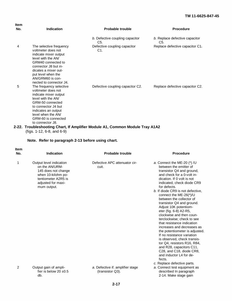
TM 11-6625-847-45
ItemNo. Indication Probable trouble Procedure
b. Defective coupling capacitor b. Replace defective capacitorC5. C5.
4 The selective frequency Defective coupling capacitor Replace defective capacitor C1.voltmeter does not C1.indicate mixer outputlevel with the AN/GRM40 connected toconnector J8 but in-dicates a mixer out-put level when theAN/GRM60 is con-nected to connector J4.
5 The frequency selective Defective coupling capacitor C2. Replace defective capacitor C2.voltmeter does notindicate mixer outputlevel with the AN/GRM-50 connectedto connector J4 butindicates an outputlevel when the AN/GRM-60 is connectedto connector J8.
2-22. Troubleshooting Chart, If Amplifier Module A1, Common Module Tray A1A2(figs. 1-12, 6-8, and 6-9)
Note. Refer to paragraph 2-13 before using chart.
ItemNo. Indication Probable trouble Procedure
1 Output level indication Defective APC attenuator cir- a. Connect the ME-20 (*) /Uon the AN/URM- cuit. between the emitter of145 does not change transistor Q4 and ground,when 10-kilohm po- and check for a 0-volt in-tentiometer A2R5 is dication. If 0 volt is notadjusted for maxi- indicated, check diode CR9mum output. for defects.
b. If diode CR9 is not defective,connect the ME-26(*)/Ubetween the collector oftransistor Q4 and ground.Adjust 10K potentiom-eter (fig. 6-8) A2-R5,clockwise and then coun-terclockwise; check to seethat resistance indicationincreases and decreases asthe potentiometer is adjusted.If no resistance variationis observed, check transis-tor Q4, resistors R16, R84,and R28, capacitors C11,C28, and C18, diode CR8,and inductor L4 for de-fects.
c. Replace defective parts.2 Output gain of ampli- a. Defective if. amplifier stage a. Connect test equipment as
fier is below 20 ±0.5 (transistor Q3). described In paragraphdb. 2-14. Make stage gain
2-17
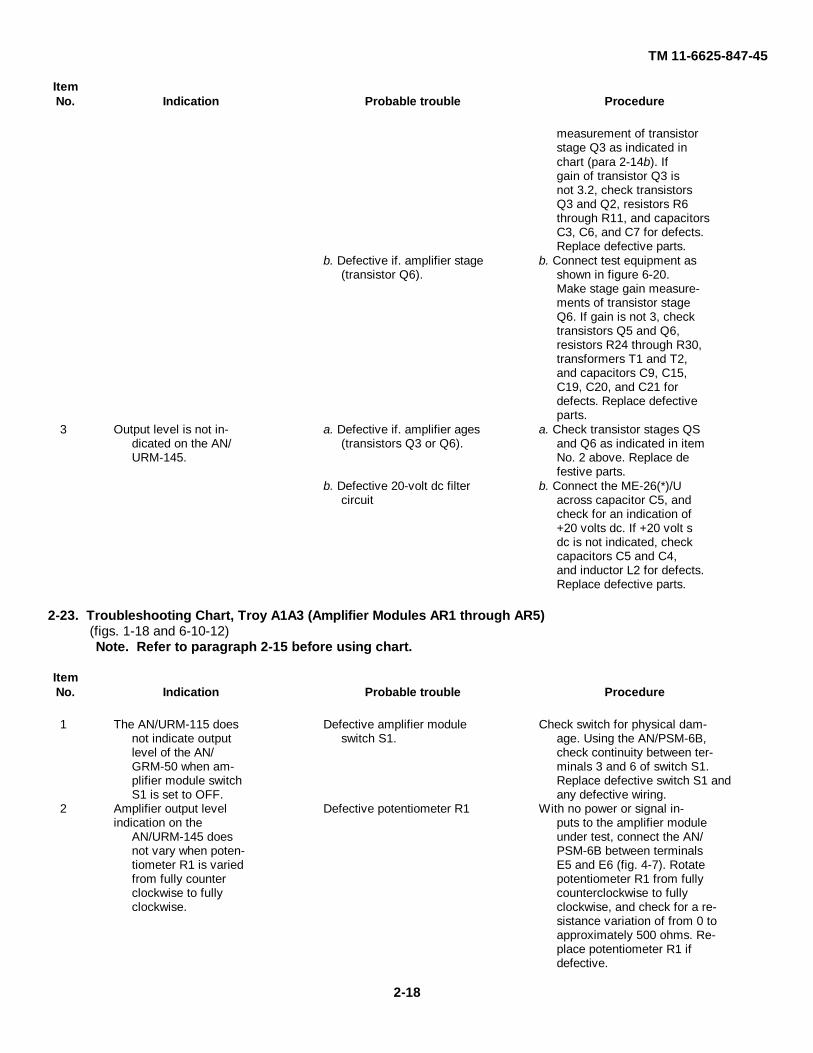
TM 11-6625-847-45
ItemNo. Indication Probable trouble Procedure
measurement of transistorstage Q3 as indicated inchart (para 2-14b). Ifgain of transistor Q3 isnot 3.2, check transistorsQ3 and Q2, resistors R6through R11, and capacitorsC3, C6, and C7 for defects.Replace defective parts.
b. Defective if. amplifier stage b. Connect test equipment as(transistor Q6). shown in figure 6-20.
Make stage gain measure-ments of transistor stageQ6. If gain is not 3, checktransistors Q5 and Q6,resistors R24 through R30,transformers T1 and T2,and capacitors C9, C15,C19, C20, and C21 fordefects. Replace defectiveparts.
3 Output level is not in- a. Defective if. amplifier ages a. Check transistor stages QSdicated on the AN/ (transistors Q3 or Q6). and Q6 as indicated in itemURM-145. No. 2 above. Replace de
festive parts.b. Defective 20-volt dc filter b. Connect the ME-26(*)/U
circuit across capacitor C5, andcheck for an indication of+20 volts dc. If +20 volt sdc is not indicated, checkcapacitors C5 and C4,and inductor L2 for defects.Replace defective parts.
2-23. Troubleshooting Chart, Troy A1A3 (Amplifier Modules AR1 through AR5)(figs. 1-18 and 6-10-12)Note. Refer to paragraph 2-15 before using chart.
ItemNo. Indication Probable trouble Procedure
1 The AN/URM-115 does Defective amplifier module Check switch for physical dam-not indicate output switch S1. age. Using the AN/PSM-6B,level of the AN/ check continuity between ter-GRM-50 when am- minals 3 and 6 of switch S1.plifier module switch Replace defective switch S1 andS1 is set to OFF. any defective wiring.
2 Amplifier output level Defective potentiometer R1 With no power or signal in-indication on the puts to the amplifier module
AN/URM-145 does under test, connect the AN/not vary when poten- PSM-6B between terminalstiometer R1 is varied E5 and E6 (fig. 4-7). Rotatefrom fully counter potentiometer R1 from fullyclockwise to fully counterclockwise to fullyclockwise. clockwise, and check for a re-
sistance variation of from 0 toapproximately 500 ohms. Re-place potentiometer R1 ifdefective.
2-18
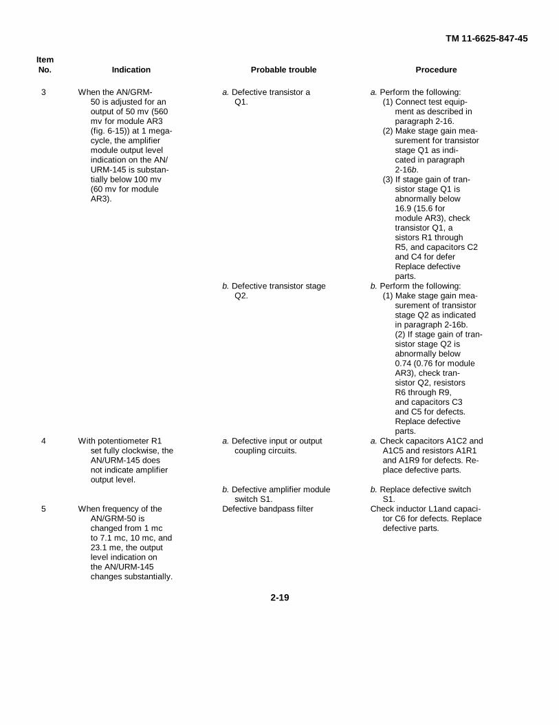
TM 11-6625-847-45
ItemNo. Indication Probable trouble Procedure
3 When the AN/GRM- a. Defective transistor a a. Perform the following:50 is adjusted for an Q1. (1) Connect test equip-output of 50 mv (560 ment as described inmv for module AR3 paragraph 2-16.(fig. 6-15)) at 1 mega- (2) Make stage gain mea-cycle, the amplifier surement for transistormodule output level stage Q1 as indi-indication on the AN/ cated in paragraphURM-145 is substan- 2-16b.tially below 100 mv (3) If stage gain of tran-(60 mv for module sistor stage Q1 isAR3). abnormally below
16.9 (15.6 formodule AR3), checktransistor Q1, asistors R1 throughR5, and capacitors C2and C4 for deferReplace defectiveparts.
b. Defective transistor stage b. Perform the following:Q2. (1) Make stage gain mea-
surement of transistorstage Q2 as indicatedin paragraph 2-16b.(2) If stage gain of tran-sistor stage Q2 isabnormally below0.74 (0.76 for moduleAR3), check tran-sistor Q2, resistorsR6 through R9,and capacitors C3and C5 for defects.Replace defectiveparts.
4 With potentiometer R1 a. Defective input or output a. Check capacitors A1C2 andset fully clockwise, the coupling circuits. A1C5 and resistors A1R1AN/URM-145 does and A1R9 for defects. Re-not indicate amplifier place defective parts.output level.
b. Defective amplifier module b. Replace defective switchswitch S1. S1.
5 When frequency of the Defective bandpass filter Check inductor L1and capaci-AN/GRM-50 is tor C6 for defects. Replacechanged from 1 mc defective parts.to 7.1 mc, 10 mc, and23.1 me, the outputlevel indication onthe AN/URM-145changes substantially.
2-19
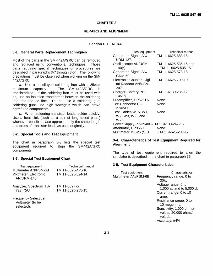
TM 11-6625-847-45
CHAPTER 3
REPAIRS AND ALIGNMENT
Section I. GENERAL
3-1. General Parts Replacement Techniques
Most of the parts in the SM-442A/GRC can be removedand replaced using conventional techniques. Thoseparts requiring special techniques or procedures aredescribed in paragraphs 3-7 through 3-54. The followingprecautions must be observed when working on the SM-442A/GRC.
a. Use a pencil-type soldering iron with a 25wattmaximum capacity. The SM-442A/GRC istransistorized. If the soldering iron must be used withac, use an isolation transformer between the solderingiron and the ac line. Do not use a soldering gun;soldering guns use high wattage’s which can proveharmful to components.
b. When soldering transistor leads, solder quickly.Use a heat sink (such as a pair of long-nosed pliers)whenever possible. Use approximately the same lengthand dress of transistor leads as used originally.
3-2. Special Tools and Test Equipment
The chart in paragraph 3-3 lists the special testequipment required to align the SM442A/GRCcomponents.
3-3. Special Test Equipment Chart
Test equipment Technical manualMultimeter AN/PSM-6B TM 11-6625-475-10Voltmeter, Electronic TM 11-6625-524-14
AN/URM-145.
Analyzer, Spectrum TS- TM 11-5097 or723 (*)/U. TM 11-6625-255-15
Frequency SelectiveVoltmeter (to beselected).
Test equipment Technical manualGenerator, Signal AN/ TM 11-6625-683-15
URM-127.Oscilloscope AN/USM- TM 11-6625-535-15 and
140(*). TM 11-6625-535-15-1Generator, Signal AN/ TM 11-6625-573-15
GRM-50.Electronic Counter, Digi- TM 11-6625-700-10
tal Readout AN/USM-207.
Charger, Battery PP- TM 11-6130-236-121451/G.
Preamplifier, HP5261A NoneTee Connector UG- None
274B/U.Test Cables W15, W1, None
W2, W3, W22 andW25.
Power Supply PP-3940G-TM 11-6130-247-15Attenuator, HP355D NoneMultimeter ME-26 (*)/U .TM 11-6625-200-12
3-4. Characteristics of Test Equipment Required forAlignment
The type of test equipment required to align thesimulator is described in the chart in paragraph 35.
3-5. Test Equipment Characteristics
Test equipment CharacteristicsMultimeter AN/PSM-6B Frequency range: 0 to
30kc.Voltage range: 0 to
1,000 ac and to 5,000 dc.Current range: 0 to 10
amp.Resistance range: 0 to
10 megohms.Sensitivity: 1,000 ohms/
volt ac 20,000 ohms/volt dc.
Accuracy: ±4%
3-1
TM 11-6625-847-45
Test equipment CharacteristicsVoltmeter, Electronic Frequency range: 0.1 mc
AN/URM-146. to 1,000 mc.Voltage range: 300
microvolts to 3 voltsrms.
Electronic Counter, Frequency range: 10 cpsDigital Readout AN/ to 100 mc.USM-207.
Frequency selective Frequency range:20 kcvoltmeter. to 30 mc.
Voltage range: 0 to 150mlllivolts.
Sensitivity: 5 megohmsGenerator, Signal AN/ Frequency range: 20 cps
URM-127. to 20 kc.Output level: 3 watts
into 600 ohms.Oscilloscope AN/USM- Frequency range: 0 to 15
140(*). mcGenerator Signal AN/ Frequency range: 2 to
GRM-50. 30 mc.Output level: 0 to 3
voltsOutput impedance-
50 ohms.Charger, Battery PP- Voltage range: 20 to
1451/G. 32 bolts.Current range: 100
amperes maximum.Preamplifier, HP 5261A Frequency counter plug-
in.
Test equipment CharacteristicsTee Connector UG- Type BNC (FSN 5986-
274B/U. 702-0125)Test Cables W16, W1, (Part of SM-442A/GRC
W2, WS, W22 and Cable Kit).W25.
Power Supply PP-3940/ Voltage range 0 to 30G. volts dc.
Current range: 150 ma(min).
Analyzer, Spectrum 20 cps to 30 kc, 10 mvTS-728(*)/U. to 1 volt, p band-
widthAttenuator, HP355D Attenuation range 0 to
110 db (FSN 5910-957-1800).
Multimeter, M#-26 (*)/U Dc voltage range: 0 to1,000 volts.
Ac voltage range: 0to 300 volts.
Resistance range: 0to 500 megohns.
Frequency range: 20cps to 700 mc.
3-6. Special Tools Chart
CA 58057 Extraction 5120-970-2722tool Cannon ElectricCo.
107-1001 Insert toolWinchester Inc.
Winchester Crimp andExtraction tool.
Section II. REPAIRS3-7. Cleaning
a. The SM-442A/GRC should be kept clean andfree of foreign matter to insure proper operation.
Warnings:1. Compressed air in dangerous andcan cause serious bodily harm. Itcan also cause mechanical damageto the equipment. Do not usecompressed air to dry parts wherecleaning compound has been used.2. Prolonged breathing of cleaningcompound is dangerous; makecertain that adequate ventilation isprovided. Cleaning compound inflammable; do not use near a flame.Avoid contact with the skin; wash offany that spills on your hands.
b. After disassembly, the mechanical componentscan be cleaned with cleaning compound (FSN7988959542). Clean switch contacts with a cloth lightlymoistened with an approved electrical contact cleaner.
3-8. InspectionAfter cleaning, inspect the disassembled mechanicalparts for the following:
a. Parts that are nicked, burred, or scratched.b. Broken or damaged gears and gear teeth.c. Damage to couplers.d. Bent or worn shafts.e. Burred bushings or bearings.f. Wires that have insulation burned or scraped
off.g. Broken wafer switch.
3-2
TM 11-6625-847-45
3-9. LubricationLubricate by applying small amounts of silicon grease(FSN 9150-257-5358) or any approved alternate, to gearteeth, shaft bushings, and bearings.
3-10. Removal of Gear Drive AssembliesTo remove the gear assemblies from tray A1A1 (fig. 3-1) and tray A1A8 (fig. 3-2), proceed as given in athrough c below.
a. Remove the bottom cover from the appropriatetray, tag and unsolder the wires connected to gear driveassembly relay K1 (fig. 3-8).
Note. Before proceeding to b belowfor tray A1A3, perform the following:
(1) Remove the setscrews from the motordriven coupler (fig. 3-4).
(2) Remove the coupler from the shaft.
b. Remove the four top panel mounting screws(fig. 3-3) that secure the gear drive assembly to eithertray A1A1 or tray A1A8. Lower and rotate the gear driveassembly outward for access.
Note. If the gear drive assembly Is tobe removed from the parent trayintact, proceed with c below;however, if the disassembly of thegear drive assembly is the finalobjective, proceed a outlined inparagraph 3-11.
c. Tag and unsolder the 28 wires connected toswitch S1 (fig. 3-3), and remove the gear driveassembly.
3-11. Disassembly of Gear Drive AssembliesTo disassemble the gear drive assembly after removalfrom tray A1A1 or tray A1A3 (para 3-10b), proceed asfollows:
a. Refer to figure 3-5; then remove the retainingring (1) from the idler gear shaft (2). Slide the Idler gear(3) off the shaft (2).
b. Remove the two retaining rings (4) from theswitch shaft, and loosen the hex setscrew (5) on theswitch gear (6).
c. Remove the two retaining rings (7) from thespur gear shaft (8).
d. Using a drift punch, drive the pins (9) from thedrive gear (22) and the spur gear (23). Loosen the hexsetscrews (10) on both gears.
e. Remove the four hex nuts (11), screws (12), flatwashers (18), and spacers (14) that secure the switchwafer (15) to the top plate (16).
f. Remove the six bottom plate screws (17),lockwashers (18), and flat washers (19), and the fourspacers (20), and remove the bottom plate (21).
g. Slide the drive gear (22), spur gear (28), andswitch gear (6) from their shafts.
h. Slide the switch shaft (24) from the wafer switchupward through the top plate.
Note. For the gear drive assemblywhen removed from tray A1A1,proceed as in (1) and (2) below.
(1) Remove the four screws (25) holding tothe top plate. Slide the coupler (26) andconnected shaft upward from the adapterbearing (27).
(2) Drive the coupler pin (28) from the shaftwith a drift punch. Loosen the hexsetscrew (29), and remove the coupler(30).
i. Remove the two hex nuts (81) and screws (32)securing the channel motor mount (88) and connectedcomponents from the top plate.
j. Drive the pin (34) from the worm gear on thechannel motor mount with a drift punch, loosen the hexsetscrew (35), and slide the worm gear (36) from themotor shaft.
k. Tag and unsolder the wires connecting thechannel motor to relay K1 (37).
l. Remove the four screws (38), four lockwashers(39), and four flat washers (40) securing the motor to thechannel motor mount. Remove the channel motor (41).
m. Remove the two hex nuts (42) and screws (43)securing the relay to the channel motor mount. Removerelay K1 (37).
3-12. Reassembly of Gear Drive Assembly(fig. 3-5)
a. Fasten the adapter bearing (27), using the fourscrews (25), to the top plate (16).
b. Slip the coupler (30) on the spur gear shaft (8),driving the coupler pins (28) Into the appropriate pinholes. Tighten the hex setscrew (29). Slide the spurgear shaft (8) through the hole in the top plate (16)through
3-3
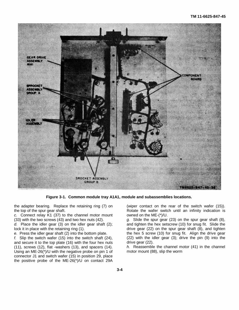
TM 11-6625-847-45
Figure 3-1. Common module tray A1A1, module and subassemblies locations.
the adapter bearing. Replace the retaining ring (7) onthe top of the spur gear shaft.c. Connect relay K1 (37) to the channel motor mount(33) with the two screws (43) and two hex nuts (42).d. Place the idler gear (3) on the idler gear shaft (2);lock it in place with the retaining ring (1).e. Press the idler gear shaft (2) into the bottom plate.f. Slip the switch wafer (15) into the switch shaft (24),and secure it to the top plate (16) with the four hex nuts(11), screws (12), flat -washers (13), and spacers (14).Using an ME-26(*)/U with the negative probe on pin 1 ofconnector J1 and switch wafer (15) in position 29, placethe positive probe of the ME-26(*)/U on contact 29A
(wiper contact on the rear of the switch wafer (15)).Rotate the wafer switch until an infinity indication isowned on the ME-(*)/U.g. Slide the spur gear (23) on the spur gear shaft (8),and tighten the hex setscrew (10) for snug fit. Slide thedrive gear (22) on the spur gear shaft (8), and tightenthe hex 5 screw (10) for snug fit. Align the drive gear(22) with the idler gear (3); drive the pin (9) into thedrive gear (22).h. Reassemble the channel motor (41) in the channelmotor mount (88), slip the worm
3-4

TM 11-6625-847-45
Figure 3-2. Synthesizer test to A1A3, module and subassemblies locations.
gear (36) on the channel motor shaft, and tighten thehex setscrew (35) for snug fit. Fasten the channel motor(41) to the channel motor mount (33) with the fourscrews (38), lockwashers (39), and flat washers (40).Attach the channel motor mount (33) to the top plate(16) with the two screws (32) and hex nuts (31).
i. Slide the switch gear (6) on the switch shaft(24); lock the switch gear to the switch on the shaft withthe retaining ring (4).
j. Secure the bottom plate with the six platescrews (17), six lockwashers (18), and six flat washers(19).
k. Align the switch gear (6) with the idler gear (3),align the drive gear (22) with the idler gear (3), and alignthe spur gear (23) with the worm gear (36). Align thenotch on the coupler (26) so that the center line of thenotch and the center line of the screw hole (44) exactly
align. Secure the gear assemblies with the appropriatepins and hex setscrews.
Note. The gear drive assemblies are nowelectrically and mechanically aligned at 29 mc.
l. If wires were unsoldered from switch S1,resolder the wires to the power terminals as indicated bythe tags.
m. Place the gear drive assembly in its properposition on the tray, and secure it with the four screwspreviously removed.
n. On tray A1A3, place the coupler on the shaftwith the pin towards the rear of tray A1A3, and secure itin position with the set screws.
3-5
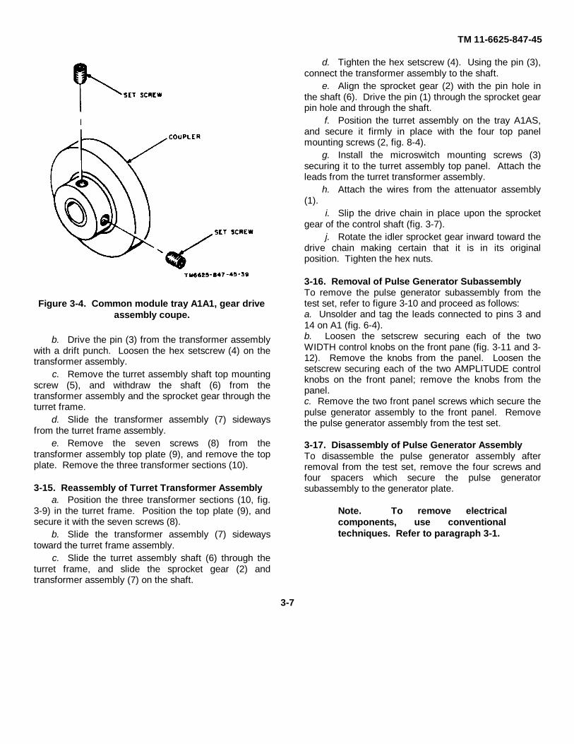
TM 11-6625-847-45
Figure 3-4. Common module tray A1A1, gear driveassembly coupe.
b. Drive the pin (3) from the transformer assemblywith a drift punch. Loosen the hex setscrew (4) on thetransformer assembly.
c. Remove the turret assembly shaft top mountingscrew (5), and withdraw the shaft (6) from thetransformer assembly and the sprocket gear through theturret frame.
d. Slide the transformer assembly (7) sidewaysfrom the turret frame assembly.
e. Remove the seven screws (8) from thetransformer assembly top plate (9), and remove the topplate. Remove the three transformer sections (10).
3-15. Reassembly of Turret Transformer Assemblya. Position the three transformer sections (10, fig.
3-9) in the turret frame. Position the top plate (9), andsecure it with the seven screws (8).
b. Slide the transformer assembly (7) sidewaystoward the turret frame assembly.
c. Slide the turret assembly shaft (6) through theturret frame, and slide the sprocket gear (2) andtransformer assembly (7) on the shaft.
d. Tighten the hex setscrew (4). Using the pin (3),connect the transformer assembly to the shaft.
e. Align the sprocket gear (2) with the pin hole inthe shaft (6). Drive the pin (1) through the sprocket gearpin hole and through the shaft.
f. Position the turret assembly on the tray A1AS,and secure it firmly in place with the four top panelmounting screws (2, fig. 8-4).
g. Install the microswitch mounting screws (3)securing it to the turret assembly top panel. Attach theleads from the turret transformer assembly.
h. Attach the wires from the attenuator assembly(1).
i. Slip the drive chain in place upon the sprocketgear of the control shaft (fig. 3-7).
j. Rotate the idler sprocket gear inward toward thedrive chain making certain that it is in its originalposition. Tighten the hex nuts.
3-16. Removal of Pulse Generator SubassemblyTo remove the pulse generator subassembly from thetest set, refer to figure 3-10 and proceed as follows:a. Unsolder and tag the leads connected to pins 3 and14 on A1 (fig. 6-4).b. Loosen the setscrew securing each of the twoWIDTH control knobs on the front pane (fig. 3-11 and 3-12). Remove the knobs from the panel. Loosen thesetscrew securing each of the two AMPLITUDE controlknobs on the front panel; remove the knobs from thepanel.c. Remove the two front panel screws which secure thepulse generator assembly to the front panel. Removethe pulse generator assembly from the test set.
3-17. Disassembly of Pulse Generator AssemblyTo disassemble the pulse generator assembly afterremoval from the test set, remove the four screws andfour spacers which secure the pulse generatorsubassembly to the generator plate.
Note. To remove electricalcomponents, use conventionaltechniques. Refer to paragraph 3-1.
3-7
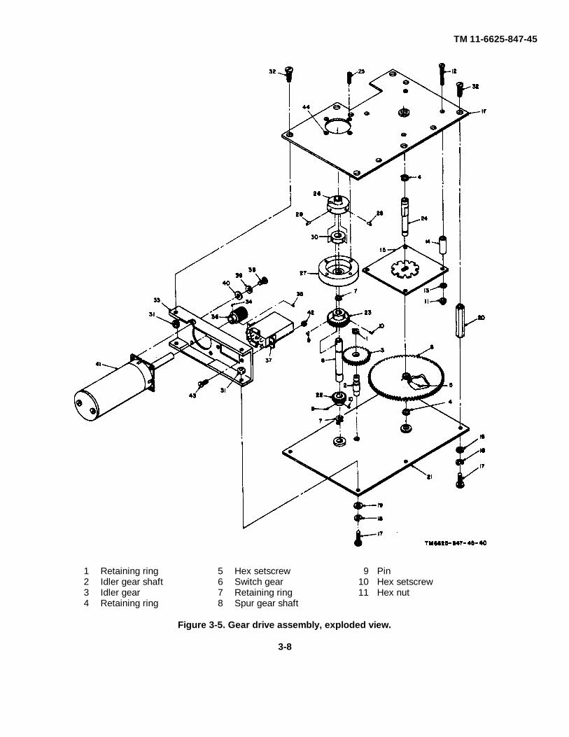
TM 11-6625-847-45
1 Retaining ring 5 Hex setscrew 9 Pin2 Idler gear shaft 6 Switch gear 10 Hex setscrew3 Idler gear 7 Retaining ring 11 Hex nut4 Retaining ring 8 Spur gear shaft
Figure 3-5. Gear drive assembly, exploded view.
3-8
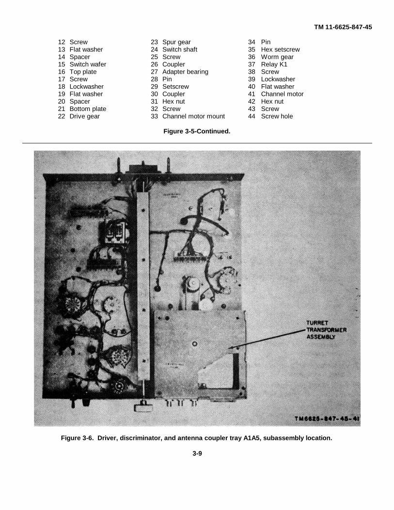
TM 11-6625-847-45
12 Screw 23 Spur gear 34 Pin13 Flat washer 24 Switch shaft 35 Hex setscrew14 Spacer 25 Screw 36 Worm gear15 Switch wafer 26 Coupler 37 Relay K116 Top plate 27 Adapter bearing 38 Screw17 Screw 28 Pin 39 Lockwasher18 Lockwasher 29 Setscrew 40 Flat washer19 Flat washer 30 Coupler 41 Channel motor20 Spacer 31 Hex nut 42 Hex nut21 Bottom plate 32 Screw 43 Screw22 Drive gear 33 Channel motor mount 44 Screw hole
Figure 3-5-Continued.
Figure 3-6. Driver, discriminator, and antenna coupler tray A1A5, subassembly location.
3-9
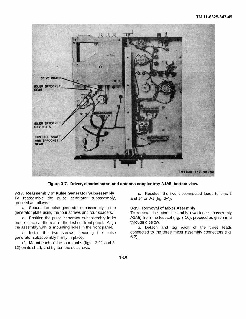
TM 11-6625-847-45
Figure 3-7. Driver, discriminator, and antenna coupler tray A1A5, bottom view.
3-18. Reassembly of Pulse Generator SubassemblyTo reassemble the pulse generator subassembly,proceed as follows:
a. Secure the pulse generator subassembly to thegenerator plate using the four screws and four spacers.
b. Position the pulse generator subassembly in itsproper place at the rear of the test set front panel. Alignthe assembly with its mounting holes in the front panel.
c. Install the two screws, securing the pulsegenerator subassembly firmly in place.
d. Mount each of the four knobs (figs. 3-11 and 3-12) on its shaft, and tighten the setscrews.
e. Resolder the two disconnected leads to pins 3and 14 on A1 (fig. 6-4).
3-19. Removal of Mixer AssemblyTo remove the mixer assembly (two-tone subassemblyA1A5) from the test set (fig. 3-10), proceed as given in athrough c below.
a. Detach and tag each of the three leadsconnected to the three mixer assembly connectors (fig.6-3).
3-10
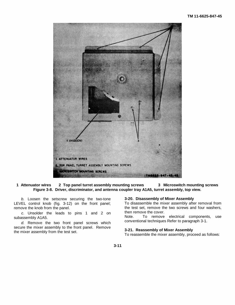
TM 11-6625-847-45
1 Attenuator wires 2 Top panel turret assembly mounting screws 3 Microswitch mounting screwsFigure 3-8. Driver, discriminator, and antenna coupler tray A1A5, turret assembly, top view.
b. Loosen the setscrew securing the two-toneLEVEL control knob (fig. 3-12) on the front panel;remove the knob from the panel.
c. Unsolder the leads to pins 1 and 2 onsubassembly A1A5.
d. Remove the two front panel screws whichsecure the mixer assembly to the front panel. Removethe mixer assembly from the test set.
3-20. Disassembly of Mixer AssemblyTo disassemble the mixer assembly after removal fromthe test set, remove the two screws and four washers,then remove the cover.Note. To remove electrical components, useconventional techniques Refer to paragraph 3-1.
3-21. Reassembly of Mixer AssemblyTo reassemble the mixer assembly, proceed as follows:
3-11
TM 11-6625-847-45
1 Pin 6 Shaft2 Sprocket gear 7 Transformer assembly3 Pin 8 Screw4 Hex Setscrew 9 Top plate5 Screw 10 Transformer section
Figure 3-9. Turrent transformer assembly, side andtop view.
a. Secure the cover of the mixer assembly firmlyin place with the two screws and four washers.
b. Position the mixer assembly in its proper place,at the rear of the test set front panel. Align theassembly with its mounting holes in the front panel.
c. Install the two screws securing the mixerassembly firmly in place.
d. Mount the LEVEL control knob on its shaft, andtighten the setscrew.
e. Resolder the two leads to pins 1 and 2 on A1A5(fig. 6-8).
f. Resolder the three leads to the three mixerassembly connectors.
3-22. Removal of Oscillator Subassemblies A2A1A2,A2A1A3, and A2A1A4To remove any of the three identical oscillatorsubassemblies A2A1A2, A2A1A3, or A2A1A4 (fig. 4-4)from the test set (fig. 3-10), proceed as given in athrough c below.
a. Unsolder and tag the leads connected tooscillator subassembly connector J2 and pin E1.
b. Loosen the setscrew securing the output levelcontrol knob on the front panel (fig. 3-11). Remove theknob.
c. Remove the three front panel screws and twowashers which secure the oscillator subassembly to thefront panel. Remove the oscillator subassembly fromthe test set.
3-23. Disassembly of Oscillator SubassembliesA2A1A2, A2A1A3 and A2A1A4To disassemble an oscillator subassembly (fig. 8-13)after removal from the test set, proceed as given in athrough d below.
a. Remove the screw (1) and two washers (2)securing the cover (3). Remove the cover.
b. Remove the metallic standoff (4).c. Remove the three screws (5) and six flat
washers (6) sewing the oscillator subassembly (7).Unsolder and tag all leads. Remove the oscillatorsubassembly from the case (8).
Note. To remove electricalcomponents, use conventionaltechniques. Refer to paragraph 3-1.
d. Disconnect and tag the leads attached to thecrystal unit (9). Remove the two nuts (10) and fourwashers (11) to remove the crystal unit (9) and crystalsocket clip (12) from the case (8).
3-12
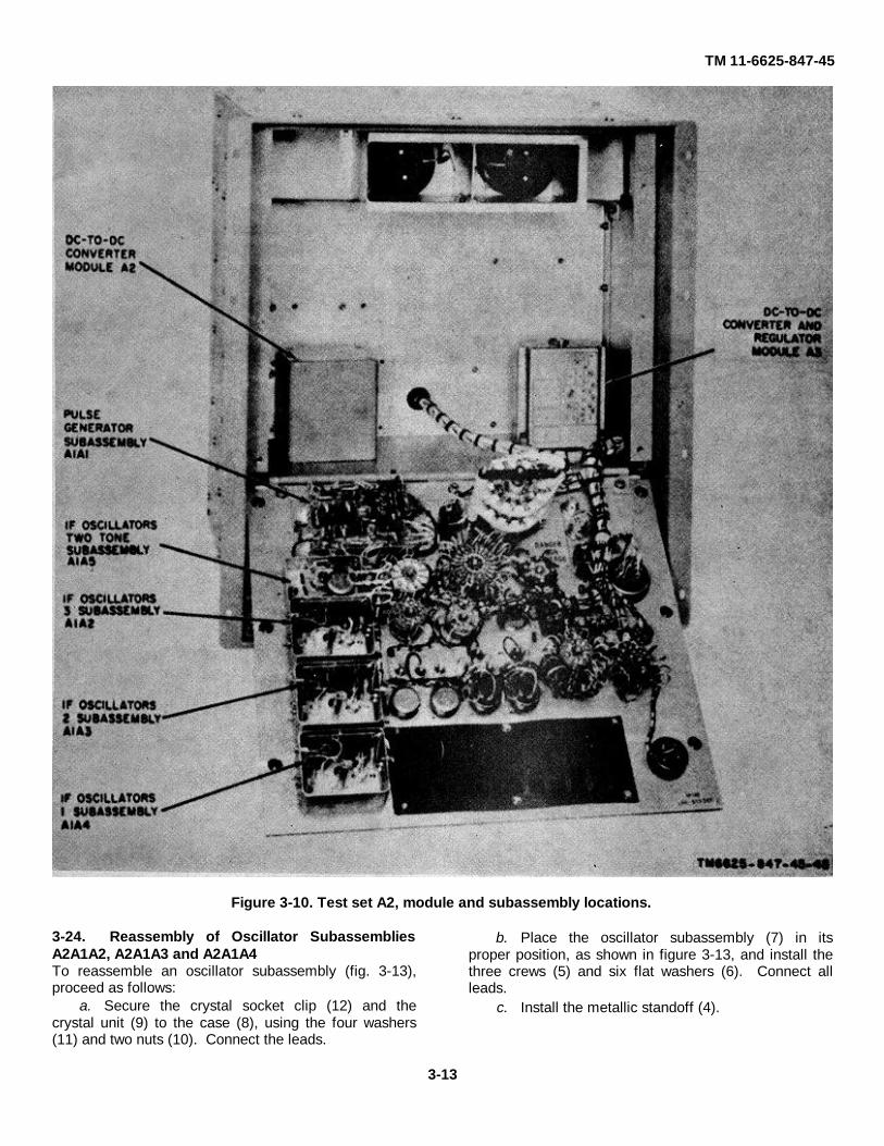
TM 11-6625-847-45
Figure 3-10. Test set A2, module and subassembly locations.
3-24. Reassembly of Oscillator SubassembliesA2A1A2, A2A1A3 and A2A1A4To reassemble an oscillator subassembly (fig. 3-13),proceed as follows:
a. Secure the crystal socket clip (12) and thecrystal unit (9) to the case (8), using the four washers(11) and two nuts (10). Connect the leads.
b. Place the oscillator subassembly (7) in itsproper position, as shown in figure 3-13, and install thethree crews (5) and six flat washers (6). Connect allleads.
c. Install the metallic standoff (4).
3-13
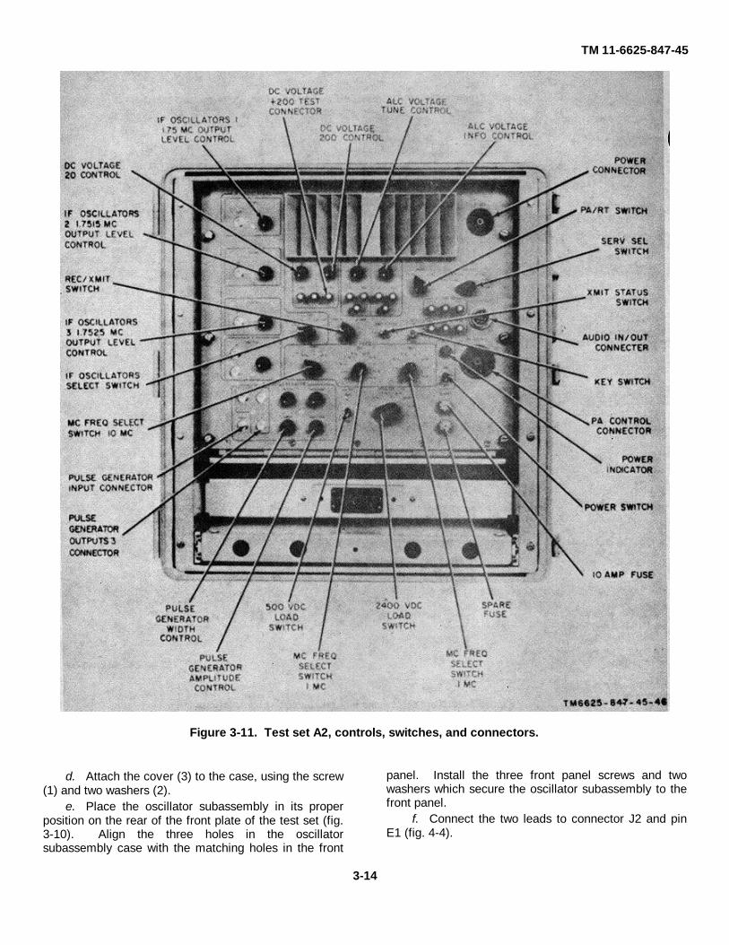
TM 11-6625-847-45
Figure 3-11. Test set A2, controls, switches, and connectors.
d. Attach the cover (3) to the case, using the screw(1) and two washers (2).
e. Place the oscillator subassembly in its properposition on the rear of the front plate of the test set (fig.3-10). Align the three holes in the oscillatorsubassembly case with the matching holes in the front
panel. Install the three front panel screws and twowashers which secure the oscillator subassembly to thefront panel.
f. Connect the two leads to connector J2 and pinE1 (fig. 4-4).
3-14
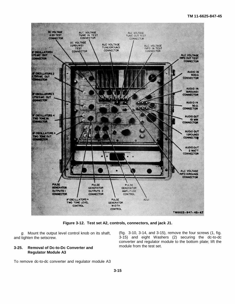
TM 11-6625-847-45
Figure 3-12. Test set A2, controls, connectors, and jack J1.
g. Mount the output level control knob on its shaft,and tighten the setscrew.
3-25. Removal of Dc-to-Dc Converter and Regulator Module A3
To remove dc-to-dc converter and regulator module A3
(fig. 3-10, 3-14, and 3-15), remove the four screws (1, fig.3-15) and eight Washers (2) securing the dc-to-dcconverter and regulator module to the bottom plate; lift themodule from the test set.
3-15
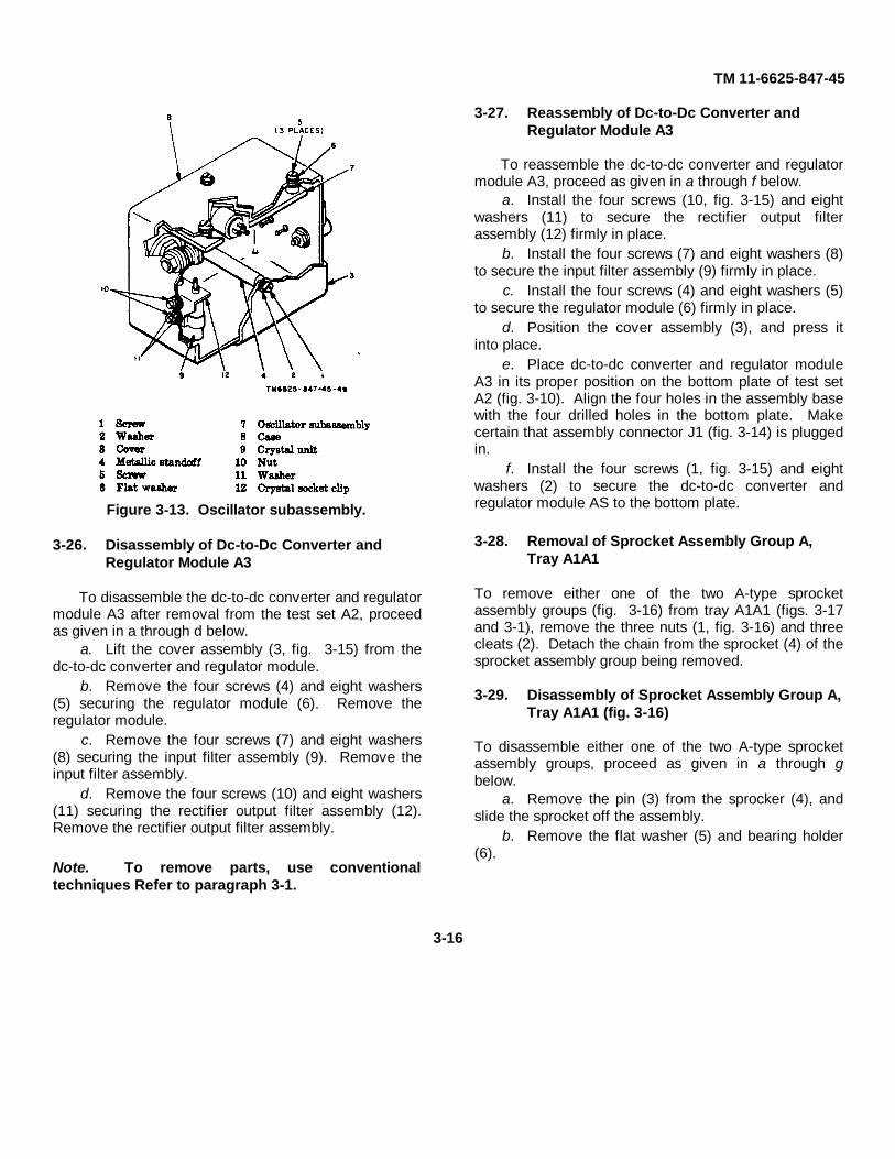
TM 11-6625-847-45
Figure 3-13. Oscillator subassembly.
3-26. Disassembly of Dc-to-Dc Converter and Regulator Module A3
To disassemble the dc-to-dc converter and regulatormodule A3 after removal from the test set A2, proceedas given in a through d below.
a. Lift the cover assembly (3, fig. 3-15) from thedc-to-dc converter and regulator module.
b. Remove the four screws (4) and eight washers(5) securing the regulator module (6). Remove theregulator module.
c. Remove the four screws (7) and eight washers(8) securing the input filter assembly (9). Remove theinput filter assembly.
d. Remove the four screws (10) and eight washers(11) securing the rectifier output filter assembly (12).Remove the rectifier output filter assembly.
Note. To remove parts, use conventionaltechniques Refer to paragraph 3-1.
3-27. Reassembly of Dc-to-Dc Converter and Regulator Module A3
To reassemble the dc-to-dc converter and regulatormodule A3, proceed as given in a through f below.
a. Install the four screws (10, fig. 3-15) and eightwashers (11) to secure the rectifier output filterassembly (12) firmly in place.
b. Install the four screws (7) and eight washers (8)to secure the input filter assembly (9) firmly in place.
c. Install the four screws (4) and eight washers (5)to secure the regulator module (6) firmly in place.
d. Position the cover assembly (3), and press itinto place.
e. Place dc-to-dc converter and regulator moduleA3 in its proper position on the bottom plate of test setA2 (fig. 3-10). Align the four holes in the assembly basewith the four drilled holes in the bottom plate. Makecertain that assembly connector J1 (fig. 3-14) is pluggedin.
f. Install the four screws (1, fig. 3-15) and eightwashers (2) to secure the dc-to-dc converter andregulator module AS to the bottom plate.
3-28. Removal of Sprocket Assembly Group A, Tray A1A1
To remove either one of the two A-type sprocketassembly groups (fig. 3-16) from tray A1A1 (figs. 3-17and 3-1), remove the three nuts (1, fig. 3-16) and threecleats (2). Detach the chain from the sprocket (4) of thesprocket assembly group being removed.
3-29. Disassembly of Sprocket Assembly Group A,Tray A1A1 (fig. 3-16)
To disassemble either one of the two A-type sprocketassembly groups, proceed as given in a through gbelow.
a. Remove the pin (3) from the sprocker (4), andslide the sprocket off the assembly.
b. Remove the flat washer (5) and bearing holder(6).
3-16
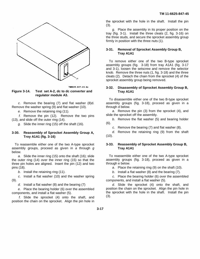
TM 11-6625-847-45
Figure 3-14. Test set A-2, dc to dc converter andregulator module A3.
c. Remove the bearing (7) and flat washer (8)d.Remove the washer spring (9) and flat washer (10).
e. Remove the retaining ring (11).f. Remove the pin (12). Remove the two pins
(13), and slide off the outer ring (14).g. Slide the inner ring (15) off the shaft (16).
3-30. Reassembly of Sprocket Assembly Group A,Troy A1A1 (fig. 3-16)
To reassemble either one of the two A-type sprocketassembly groups, proceed as given in a through gbelow.
a. Slide the inner ring (15) onto the shaft (16); slidethe outer ring (14) over the inner ring (15) so that thethree pin holes are aligned. Insert the pin (12) and twopins (18).
b. Install the retaining ring (11).c. Install a flat washer (10) and the washer spring
(9).d. Install a flat washer (8) and the bearing (7)e. Place the bearing holder (6) over the assembled
components, and install a flat washer (5).f. Slide the sprocket (4) onto the shaft, and
position the chain on the sprocket. Align the pin hole in
the sprocket with the hole in the shaft. Install the pin(3).
g. Place the assembly in its proper position on thetray (fig. 3-1). Install the three cleats (2, fig. 3-16) onthe three studs, and secure the sprocket assembly groupfirmly in position with the three nuts (1).
3-31. Removal of Sprocket Assembly Group B, Tray A1A1
To remove either one of the two B-type sprocketassembly groups (fig. 3-18) from tray A1A1 (fig. 3-17and 3-1), loosen the setscrew and remove the selectorknob. Remove the three nuts (1, fig. 3-18) and the threecleats (2). Detach the chain from the sprocket (4) of thesprocket assembly group being removed.
3-32. Disassembly of Sprocket Assembly Group B,Tray A1A1
To disassemble either one of the two B-type sprocketassembly groups (fig. 3-18), proceed as given in athrough d below.
a. Remove the pin (3) from the sprocket (4), andslide the sprocket off the assembly.
b. Remove the flat washer (5) and bearing holder(6).
c. Remove the bearing (7) and flat washer (8).d. Remove the retaining ring (9) from the shaft
(10).
3-33. Reassembly of Sprocket Assembly Group B, Tray A1A1
To reassemble either one of the two A-type sprocketassembly groups (fig. 3-18), proceed as given in athrough e below.
a. Place the retaining ring (9) on the shaft (10).b. Install a flat washer (8) and the bearing (7).c. Place the bearing holder (6) over the assembled
components, and install a flat washer (5).d. Slide the sprocket (4) onto the shaft, and
position the chain on the sprocket. Align the pin hole inthe sprocket with the hole in the shaft. Install the pin(3).
3-17
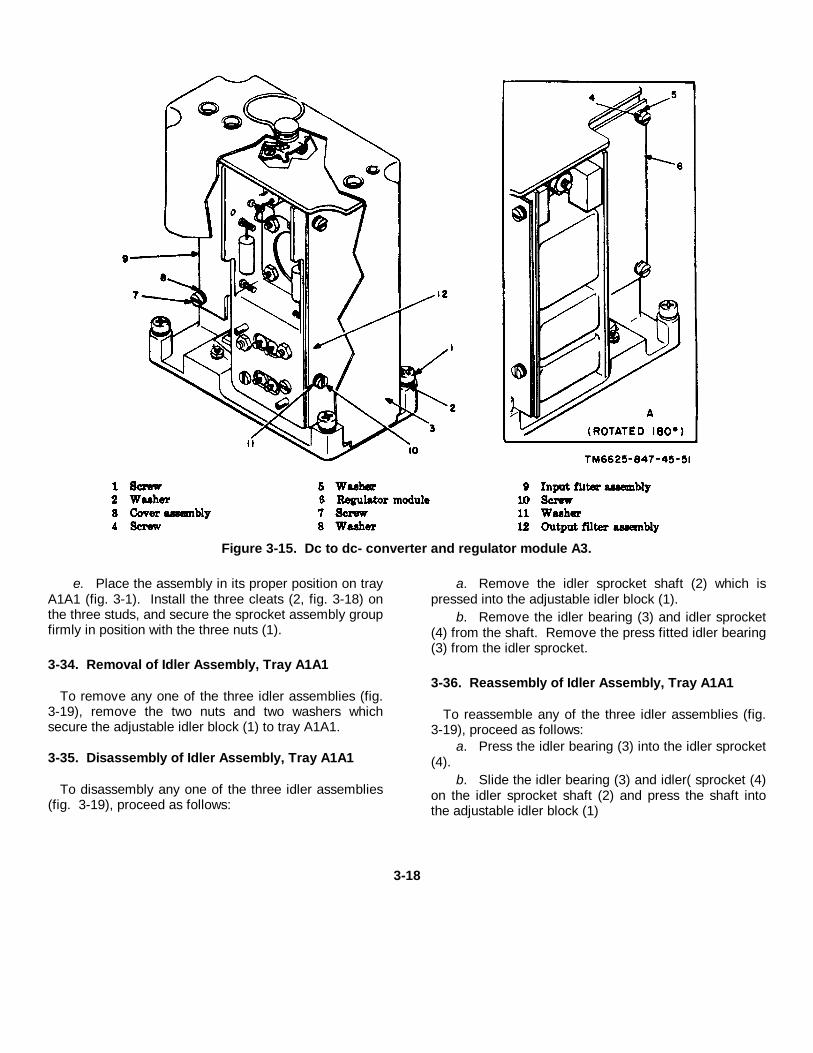
Figure 3-15. Dc to dc- converter and regulator module A3.
e. Place the assembly in its proper position on trayA1A1 (fig. 3-1). Install the three cleats (2, fig. 3-18) onthe three studs, and secure the sprocket assembly groupfirmly in position with the three nuts (1).
3-34. Removal of Idler Assembly, Tray A1A1
To remove any one of the three idler assemblies (fig.3-19), remove the two nuts and two washers whichsecure the adjustable idler block (1) to tray A1A1.
3-35. Disassembly of Idler Assembly, Tray A1A1
To disassembly any one of the three idler assemblies(fig. 3-19), proceed as follows:
a. Remove the idler sprocket shaft (2) which ispressed into the adjustable idler block (1).
b. Remove the idler bearing (3) and idler sprocket(4) from the shaft. Remove the press fitted idler bearing(3) from the idler sprocket.
3-36. Reassembly of Idler Assembly, Tray A1A1
To reassemble any of the three idler assemblies (fig.3-19), proceed as follows:
a. Press the idler bearing (3) into the idler sprocket(4).
b. Slide the idler bearing (3) and idler( sprocket (4)on the idler sprocket shaft (2) and press the shaft intothe adjustable idler block (1)
3-18
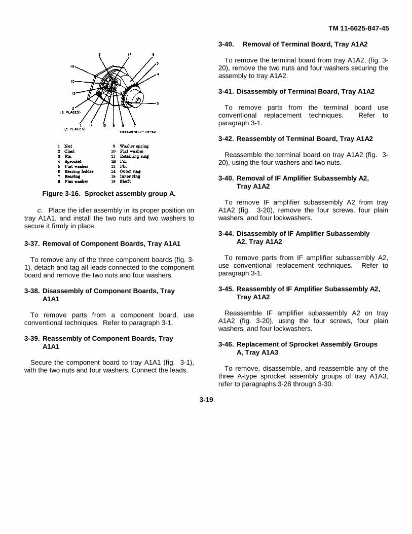
TM 11-6625-847-45
Figure 3-16. Sprocket assembly group A.
c. Place the idler assembly in its proper position ontray A1A1, and install the two nuts and two washers tosecure it firmly in place.
3-37. Removal of Component Boards, Tray A1A1
To remove any of the three component boards (fig. 3-1), detach and tag all leads connected to the componentboard and remove the two nuts and four washers.
3-38. Disassembly of Component Boards, Tray A1A1
To remove parts from a component board, useconventional techniques. Refer to paragraph 3-1.
3-39. Reassembly of Component Boards, Tray A1A1
Secure the component board to tray A1A1 (fig. 3-1),with the two nuts and four washers. Connect the leads.
3-40. Removal of Terminal Board, Tray A1A2
To remove the terminal board from tray A1A2, (fig. 3-20), remove the two nuts and four washers securing theassembly to tray A1A2.
3-41. Disassembly of Terminal Board, Tray A1A2
To remove parts from the terminal board useconventional replacement techniques. Refer toparagraph 3-1.
3-42. Reassembly of Terminal Board, Tray A1A2
Reassemble the terminal board on tray A1A2 (fig. 3-20), using the four washers and two nuts.
3-40. Removal of IF Amplifier Subassembly A2, Tray A1A2
To remove IF amplifier subassembly A2 from trayA1A2 (fig. 3-20), remove the four screws, four plainwashers, and four lockwashers.
3-44. Disassembly of IF Amplifier Subassembly A2, Tray A1A2
To remove parts from IF amplifier subassembly A2,use conventional replacement techniques. Refer toparagraph 3-1.
3-45. Reassembly of IF Amplifier Subassembly A2, Tray A1A2
Reassemble IF amplifier subassembly A2 on trayA1A2 (fig. 3-20), using the four screws, four plainwashers, and four lockwashers.
3-46. Replacement of Sprocket Assembly Groups A, Tray A1A3
To remove, disassemble, and reassemble any of thethree A-type sprocket assembly groups of tray A1A3,refer to paragraphs 3-28 through 3-30.
3-19
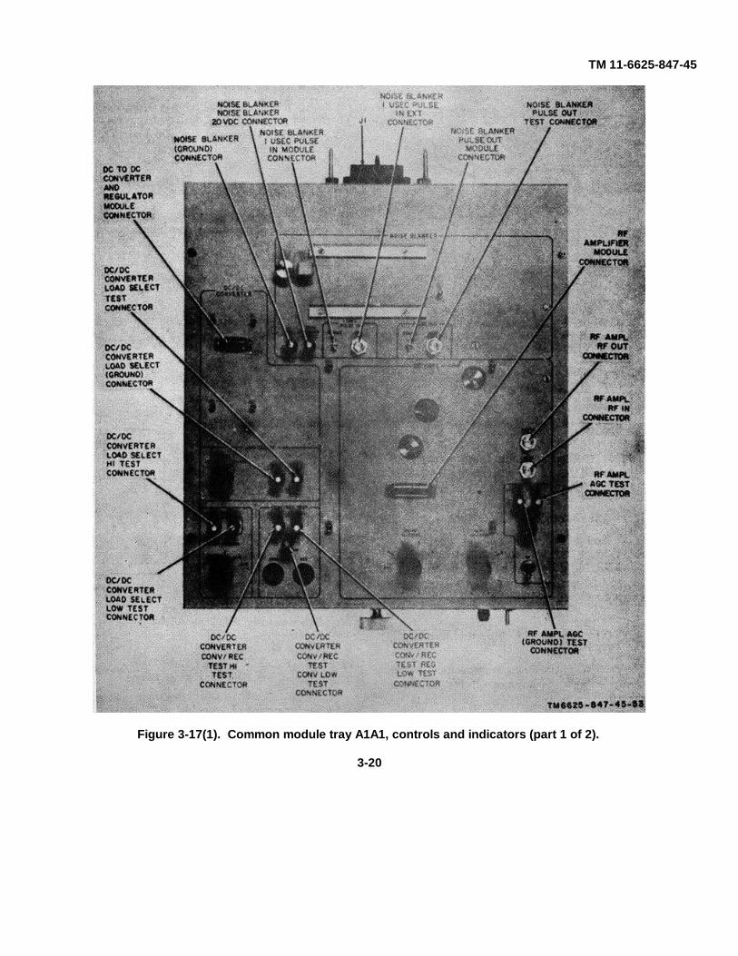
TM 11-6625-847-45
Figure 3-17(1). Common module tray A1A1, controls and indicators (part 1 of 2).
3-20
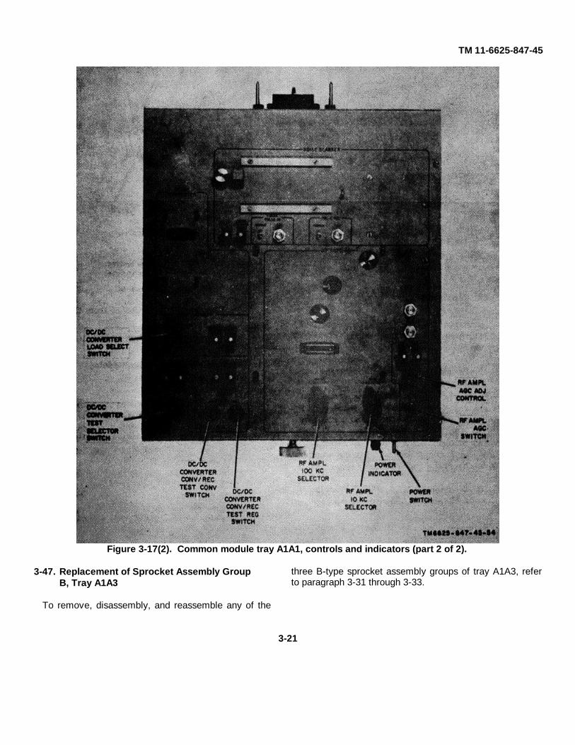
TM 11-6625-847-45
Figure 3-17(2). Common module tray A1A1, controls and indicators (part 2 of 2).
3-47. Replacement of Sprocket Assembly Group B, Tray A1A3
To remove, disassembly, and reassemble any of the
three B-type sprocket assembly groups of tray A1A3, referto paragraph 3-31 through 3-33.
3-21
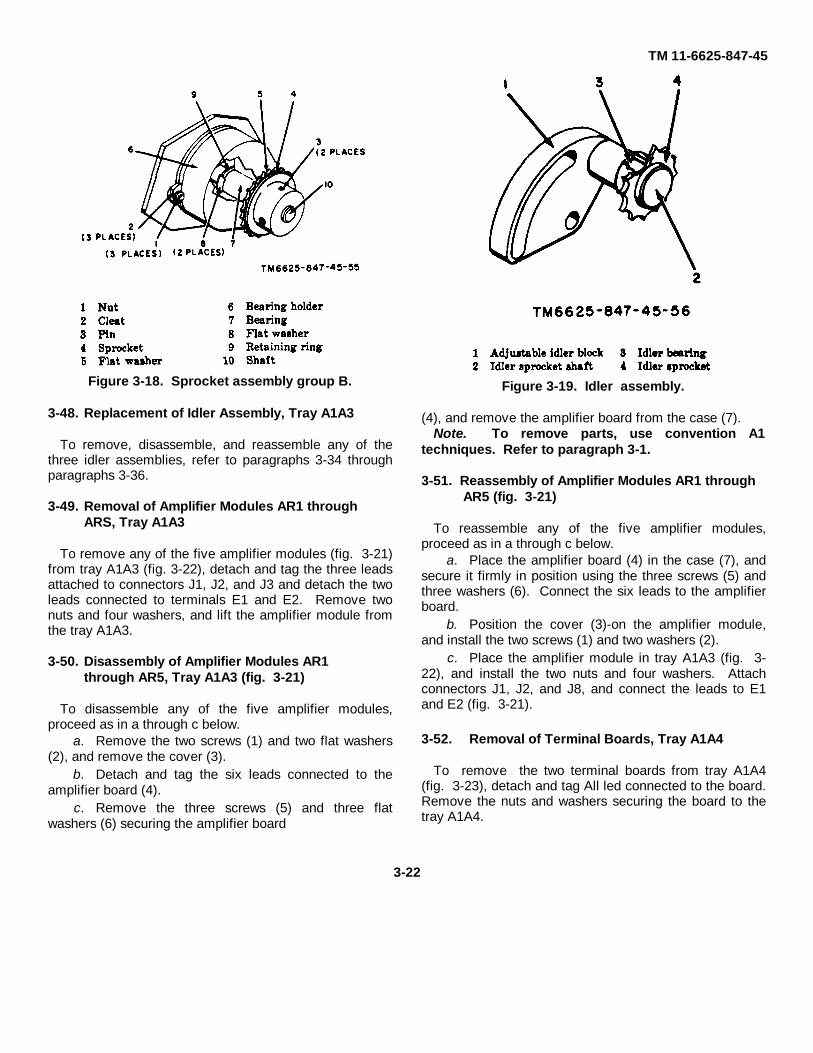
TM 11-6625-847-45
Figure 3-18. Sprocket assembly group B.
3-48. Replacement of Idler Assembly, Tray A1A3
To remove, disassemble, and reassemble any of thethree idler assemblies, refer to paragraphs 3-34 throughparagraphs 3-36.
3-49. Removal of Amplifier Modules AR1 through ARS, Tray A1A3
To remove any of the five amplifier modules (fig. 3-21)from tray A1A3 (fig. 3-22), detach and tag the three leadsattached to connectors J1, J2, and J3 and detach the twoleads connected to terminals E1 and E2. Remove twonuts and four washers, and lift the amplifier module fromthe tray A1A3.
3-50. Disassembly of Amplifier Modules AR1 through AR5, Tray A1A3 (fig. 3-21)
To disassemble any of the five amplifier modules,proceed as in a through c below.
a. Remove the two screws (1) and two flat washers(2), and remove the cover (3).
b. Detach and tag the six leads connected to theamplifier board (4).
c. Remove the three screws (5) and three flatwashers (6) securing the amplifier board
Figure 3-19. Idler assembly.
(4), and remove the amplifier board from the case (7).Note. To remove parts, use convention A1
techniques. Refer to paragraph 3-1.
3-51. Reassembly of Amplifier Modules AR1 through AR5 (fig. 3-21)
To reassemble any of the five amplifier modules,proceed as in a through c below.
a. Place the amplifier board (4) in the case (7), andsecure it firmly in position using the three screws (5) andthree washers (6). Connect the six leads to the amplifierboard.
b. Position the cover (3)-on the amplifier module,and install the two screws (1) and two washers (2).
c. Place the amplifier module in tray A1A3 (fig. 3-22), and install the two nuts and four washers. Attachconnectors J1, J2, and J8, and connect the leads to E1and E2 (fig. 3-21).
3-52. Removal of Terminal Boards, Tray A1A4
To remove the two terminal boards from tray A1A4(fig. 3-23), detach and tag All led connected to the board.Remove the nuts and washers securing the board to thetray A1A4.
3-22
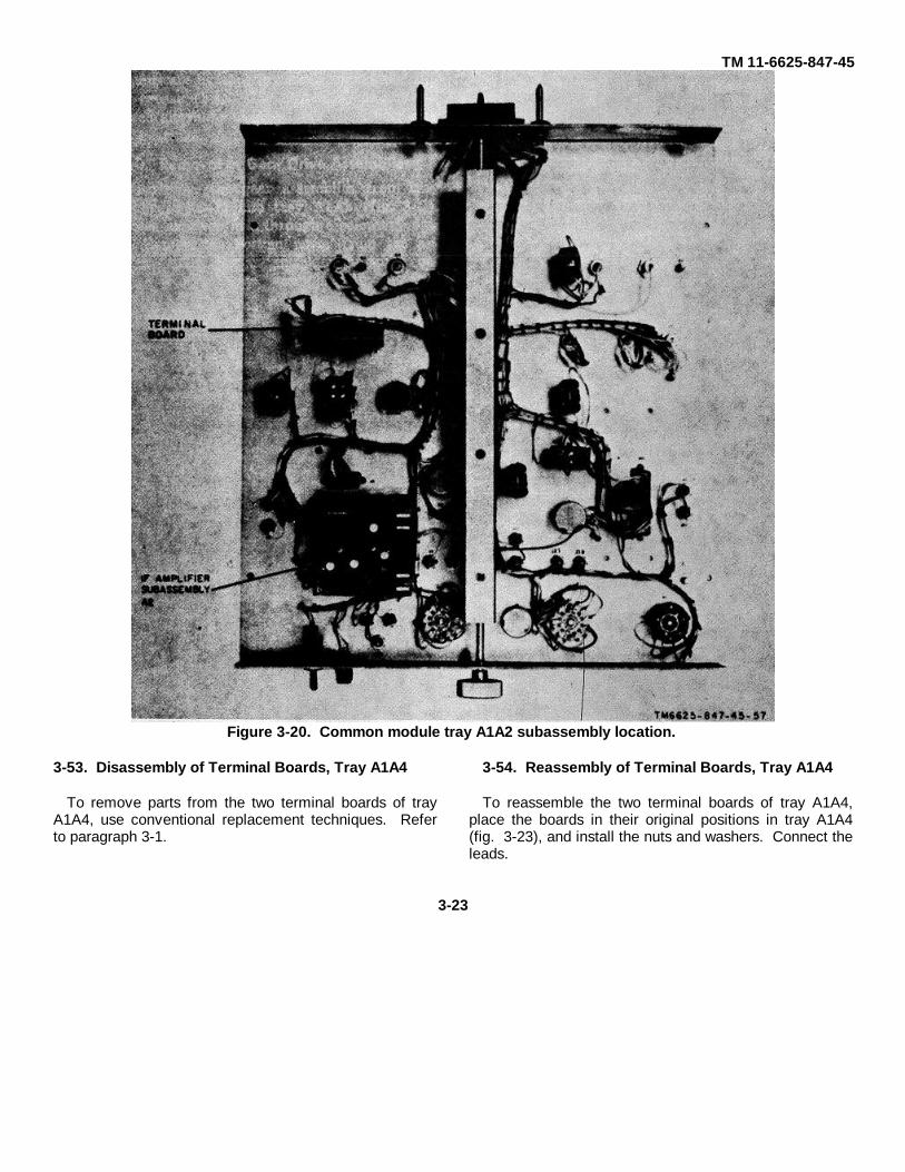
TM 11-6625-847-45
Figure 3-20. Common module tray A1A2 subassembly location.
3-53. Disassembly of Terminal Boards, Tray A1A4
To remove parts from the two terminal boards of trayA1A4, use conventional replacement techniques. Referto paragraph 3-1.
3-54. Reassembly of Terminal Boards, Tray A1A4
To reassemble the two terminal boards of tray A1A4,place the boards in their original positions in tray A1A4(fig. 3-23), and install the nuts and washers. Connect theleads.
3-23
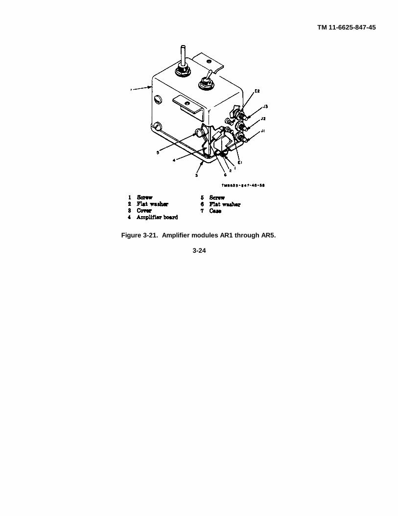
TM 11-6625-847-45
Figure 3-21. Amplifier modules AR1 through AR5.
3-24
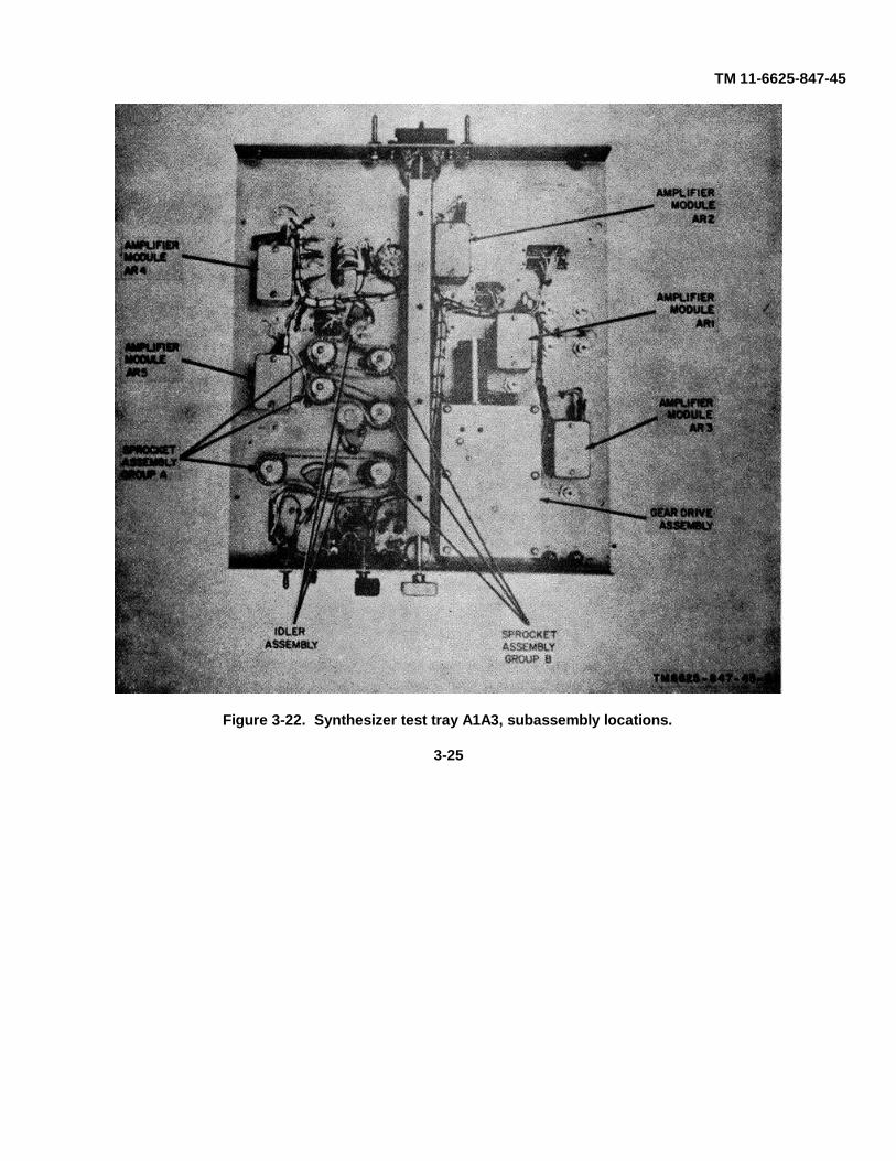
TM 11-6625-847-45
Figure 3-22. Synthesizer test tray A1A3, subassembly locations.
3-25
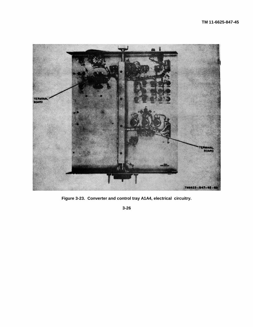
TM 11-6625-847-45
Figure 3-23. Converter and control tray A1A4, electrical circuitry.
3-26
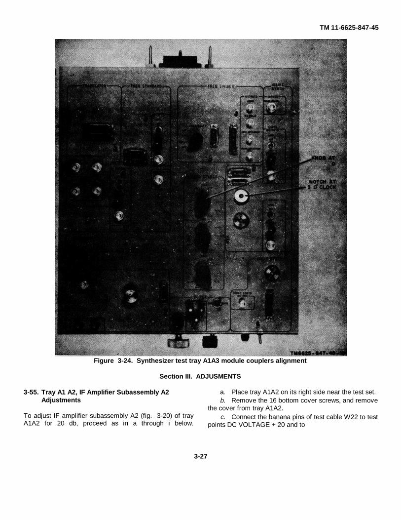
TM 11-6625-847-45
Figure 3-24. Synthesizer test tray A1A3 module couplers alignment
Section III. ADJUSMENTS
3-55. Tray A1 A2, IF Amplifier Subassembly A2 Adjustments
To adjust IF amplifier subassembly A2 (fig. 3-20) of trayA1A2 for 20 db, proceed as in a through i below.
a. Place tray A1A2 on its right side near the test set.b. Remove the 16 bottom cover screws, and remove
the cover from tray A1A2.c. Connect the banana pins of test cable W22 to test
points DC VOLTAGE + 20 and to
3-27
TM 11-6625-847-45
ground on the test set. Connect the clips at theremaining end of cable W22 to terminal A1E11 (+20volts dc) and to A1E8 (ground) on tray A1A2 (fig. 4-6),and connect a jumper wire from terminal A1E11 toterminal A1E4.
d. Using test cable W25, connect the rf outputconnector of Generator, Signal AN/GRM-50 to terminalA1E3. Ground the AN/GRM50 to terminal A1E2. Setthe output of the AN/ GRM-50 at terminal A1E3 to 1 mv.
e. Connect the AN/URM-145 to the RCVR IF testconnector and AMPL IF OUT on tray A1A2.
f. Set the test set POWER switch to ON, androtate the SERV SEL switch to OVEN ON.
g. With the ME-26(*)/U, adjust the voltage atterminal A1E11 (fig. 4-6) for +20 volts dc, using the DCVOLTAGE 20 control on the test set to adjust the level.
h. Adjust resistor A2R5 (fig. 6-8) until theAN/GRM-50 indicates a gain of 20 ±0.6 db at the outputof if. amplifier Subassembly A2.
Note. With a 1-mv input level a 20-bd gain amplifierwill indicate with equal input and output impedance,an output voltage level of 10 mv.
i. Rotate the SERV SEL switch on the test set toOFF. Set the test set POWER switch to OFF, anddisconnect All test equipment. Replace the bottomcover, and secure it with the screws removed in babove.
3-56. Tray A1A2 Adjustment (fig. 3-24)
a. The proper relationship between-the position ofthe 10 & 1 KC SYNTH and 100 KC SYNTH modulecouplers are the associated FREQ SELECT knobposition is required to provide the proper operatingfrequency of the plug-in module when installed on trayA1A2. The couplers notch should be positioned at 3o'clock when viewed from the front of the chassis, andthe associated knob at 0. Establish this relationship byfirst rotating the knob until the coupler is positionedproperly, then loosening the Allen setscrews on theknob, repositioning the knob to 0, and retightening theAllen setscrews.
b. To adjust the drive chain tension, loosen thenuts seeming the idler assembly until the chain is firmbut not taut. When the proper drive chain tension isattained, tighten the nub securing the idler assembly inposition.
3-28
TM 11-6625-847-45CHAPTER 4
GENERA1 SUPPORT TESTING PROCEDURES
4-1. Generala. Testing procedures are prepared for use by
Signal Field Maintenance Shops and Signal ServiceOrganizations responsible for general supportmaintenance of signal equipment to determine theacceptability of repaired equipment. These proceduresset forth specific requirements that repaired equipmentmust meet before it is returned to the using organization.
b. Comply with the instructions preceding each chartbefore proceeding to the chart. Perform each step insequence. Do not vary the sequence. For each step,perform All the actions required in the Teat equipmentcontrol settings column; then set the controls and switcheson the module or subassembly being tested to thepositions indicated in the Equipment under test controlsettings column; then perform each specific test
procedure and verify it against its performance standard.If a performance standard is not met while testing amodule or subassembly, refer to the applicabletroubleshooting chart for corrective measures as indicatedunder the performance standard.
4-2. Test Equipment, Tools, and Materials
All test equipment, tools, materials, and otherequipment required to perform the testing proceduresgiven in this section are listed in the charts in a through dbelow, and are authorized under TA 11-17, Signal FieldMaintenance Shops, and TA 11-100(11-17), Allowancesof Signal Corps Expendable Supplies for Signal FieldMaintenance Shop, Continental United States.
a. Test Equipment.Nomenclature Federal stock No. Technical manual
Multimeter AN/PSM-6B - ............................................ 6625-643-1688 TM 11 6625-475-10Voltmeter, Electronic AN/URM- 6625-973-3986 TM 11-6625-524-14
145.Electric Counter, Digital 6625-911-6368 TM 11-6625-700-10Readout AN/USM-207.Frequency Selective Voltmeter .................................... None NoneGenerator, Signal AN/URM- 6625-783-5965 TM 11-6625-683-15
127.Oscilloscope AN/USM-140(*)- ..................................... 6625-066-2525 TM 11-6625-535-15Generator, Signal AN/GRM- 6625-868-8353 TM 11-6625-573-15Analyzer, Spectrum TS-723(*)/ 6625-668-9418 TM 11-5097U.
b. Tools. ToolFederal Stock No. 107-1001 Inert tool, None
ToolFederal stock No. Winchester Inc.Tool Kit, Electronic5180-605-0079 Winchester Crimp and None
Equipment TK-100/G. Extraction tool. Amp Inc.Crimp Tools NoneTool Kit, Electronic Equip-5180-610-8177 Crimp Tool, Thomas & None
ment TK-105/G. Betes Co. No. WT-GA 58037 Extraction5120-970-2722 219
tool, Cannon Electric Screwdriver with screw- NoneCo. holding clip.
4-1
TM 11-6625-847-45c. Other Equipment.
EquipmentFederal stock No.Technical ManualCharger, Battery PP-1451/G6130-985-8157 ...........TM 11-6130-236-12Preamplifier, HP5261A NoneNoneTee Connector UG-274B/U NoneNone
BNC Type.Test Cables W15, W1, W2, NoneNone
W3, W22, and W25.Power Supply PP-3940/G6130-985-8167TM 11-6130-247-15Attenuator HP355D 5910-957-1860NoneCable Assembly, Radio Frequency NoneNone
d. Materials (for Fabrication of Special Test Cables).
Material Qtyreqd Federal stock No
Resistor, fixed composition 1 5905-185-85110,000 ohms ±5%;1 watt.
Resistor, fixed composition 1560 dns ±5%;1/2 watt.
Resistor, fixed composition 12000 ohms ±5%;1/2 watt.
Resistor, fixed composition 851 ohms ±5%;1/2 watt
Resistor, fixed, wire 1wound: 1000 ohms±5%; 50 watt.
Resistor, fixed, wire 1wound: 250 ohms ±5%;15 watt
Resistor, variable composition 1500 ohms ±20%;50 watt
Resistor, variable, composition 110,000 ohms±20%; 2 watts.
Capacitor, fixed, ceramic 20.01 uf ± 10%; 50 vdcw.
Connector UG-1460/U 4Selector #5051 BNC 2
Connector (with two6 inch pieces of RG-196/U coax).
#22 AWG insulated wire 1(6 inches).
Resistor, fixed composition 12,490 ohms, 10watts
Resistor, fixed, wire- 1wound, 8.45 ohms,10 watts
4-3. Power Supply for General Support Tests
The general support tests given in paragraphs 4-5through paragraph 4-11 require 20-, 30, and 27-volts dc(adjustable) power supplies. If standard power suppliesare not available, the + 20-volt dc supply can be obtainedfrom the front panel of the test set at DC VOLTAGE testpoints +20 and (ground). The -33 volt dc supply isobtained across test points RCVR IF III and LO oncommon module tray A1A2, connected to the test set andenergized, with the RCVR IF TEST SELECTOR switchset to position 1.
4-4. Test Setups and Fabrication of Test Cables
Figures 4-1 through Figure 4-7 and Figure 6-15 throughFigure 6-21 illustrate the necessary test setups requiredfor completion of the general support tests of the modulesand subassemblies of the SM-442A/GRC. The modulesand subassemblies being tested are contained in the testset, common module tray A1A2, and synthesizer test trayA1A3. Common module tray A1, converter and controltray A4, and driver, discriminator, and antenna couplertray A1A5 do not have any modules or subassembliesthat require general support testing. When necessary, thefabrication of special test cables is illustrated on theappropriate test setup illustration. The cheat in paragraph4-2d lists the materials needed for the fabrication of thespecial.
Change 1 4-2
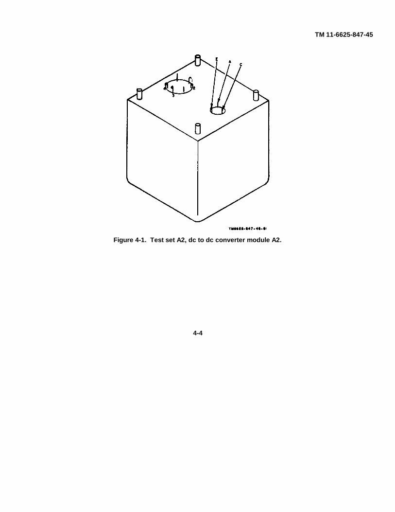
TM 11-6625-847-45
Figure 4-1. Test set A2, dc to dc converter module A2.
4-4
TM 11-6625-847-45
4-5. Test Set A2, Dc-to-Dc Converter Module A2; Voltage, Regulation, and Ripple Tests
Dc-to-dc converter module A2 (fig. 4-1) (module A2) is on the boom plate in the beck of the front panel of the testset (fig. 3-10) and is secured by four hexagonal nuts. Module A2 (fig. 4-1) is an encapsulated unit and is not repairable.If any of the performance standards are not satisfied, replace module A2.
a. Test Equipment and Materials,(1) Multimeter AN/PSM-6B.(2) Oscilloscope AN/USM-140.(3) Resistor: 1,000 ohms, 50 watts.(4) Charger, Battery PP-1451/G.(5) Resistor: 260 ohms, 15 watts.
b. Test Connections and Conditions. Connect the equipment as shown in figure 6-15.c. Procedure.
Step Control settingsNo. Test equipment Equipment under test Test procedure1 AN/PSM-6B POWER switch: OFF a. Set the DC VOLTAGE 200
The voltage should vary fromFUNCTION switch: SERV SEL switch: OFF control to approximately less than +190 volts dc to
DCV-20KΩ/V. PA/RT switch: PA midrange. more then +210 volts dc. SetRANGE switch: 250. KEY switch: OFF b. Connect the AN/PSM-6B dc the voltage to +
XMIT STATUS switch: OPR test leads to the PP-1451/REC-XMIT switch: REC G output terminals toALC VOLTAGE INFO control: check the output voltage.
Fully counterclockwise c. Set the PP-1451/G NORMALALC VOLTAGE TUNE con- CHARGE switch to NOR-
trol: Fully counterclockwise MAL and the power switchIF OSCILLATOR select switch: ON. Set the VOLTAGE
4. ADJUST control for anMC FREQ 10MC switch: 0 output of +27 volts dc onMC FREQ 1MC switch: 0 the AN/PSM-6B.MC FREQ 1MC switch: 0 d. Turn the PP-1451/G power500 VDC LOAD switch: LOW switch to OFF, and discon-2400 VDC LOAD switch: 1 nect the AN/PSM-6B.
e. Connect the AN/PSM-6Bacross terminals 3 and 4of module A2 between+200 DC VOLTAGE testpoint A1J3, on the frontpanel of the test set andDC VOLTAGE (ground)test connector A1J2.
f Turn the test set SERV SELswitch to OVEN ON andthe power switch to ON;set the PP-1451/G powerswitch to ON.
g. Turn the DC VOLTAGE200 control from fullycounterclockwise to fullyclockwise.
h. Turn the PP-1461/G powerswitch to OFF, and thetest set power switch toOFF.
2 Same as step 1 above. Same as step 1 above. a. Connect the AN/PSM-6B1% of the value in step 1 above.
dc test leads to the PP-1451/G output terminals.Energize the PP-1451/G.Adjust the output voltageto +26 volts or to +24volts if the PP-1451/Gcan be adjusted to that lowvalue. Turn the PP-1451/Goff, and remove the AN/PSM-6B leads.
b. Connect the AN/PSM-6Bbetween test points DCVOLTAGE +200 and DCVOLTAGE (ground) onthe test set.
c. Turn the PP-1451/G powerswitch and the test setPOWER switch to ON.
d. While monitoring the AN/PSM-6B, adjust the DCVOLTAGE 200 controlfrom fully counterclock-wise to fully clock-wise.
e. Turn the PP-1451/G powerswitch and the test setPOWER switch to OFF.
f. Repeat the procedures in athrough e above with thePP-1451/G set at +30volts dc.
g. Return the PP-1451/G out-put to 27 volts, after com-pletion of f above. Turnthe power switch to OFF.
3. AN/USM-140(*) Same as step 1 above. a. Connect the AN/USM-140(*)Ripple shall not be greaterAdjust the AN/USM- test probe between test than 0.2% rms of the output
140(*) controls to points DC VOLTAGE +200 voltage.the setting required and DC VOLTAGEto monitor the ripe (ground) on the test setpie on a segment of b. Turn the PP-4461/G powerthe +200-volt dc switch to ON.output. c. Monitor the ripple on a seg-
ment of the +200-volt dcoutput.
d. Turn the power switch onPP-1451/G and the POWERswitch on the test set toOFF.
4-5
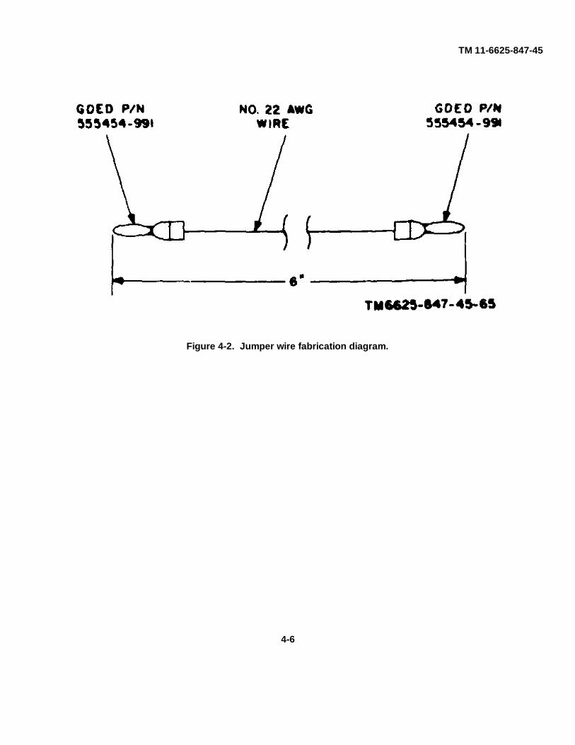
TM 11-6625-847-45
Figure 4-2. Jumper wire fabrication diagram.
4-6
TM 11-6625-847-45
4-6. Test Set A2, Dc-to-Dc Converter and Regulator Module A3 Tests
Dc-to-dc converter and regulator module AS (module A3) (fig. 3-10) is in the bank of the test set front panel and is secured to the bottom plate by four captivescrews. The general support test of this module utilizes the test set as test equipment.
a. Test Equipment and Materials.(1) Multimeter AN/PSM-6B.(2) Oscilloscope AN/USM-140(*).(3) Charger, Battery PP-1451/G.(4) One each of the following load resistors:
(a) 39 ohms, 25 watts.(b) 10,000 ohms, 1 watt.(c) 2,490 ohms, 10 watts.(d) 8.45 ohms, 10 watts.
(5) Fabricate the -test cable as shown in figure 4-2.b. Test Connections and Conditions. Connect the equipment as shown in figure 6-16.c. Procedure.
Step Control settingsNo. Test equipment Equipment under test Test procedure Performance standard1 AN/PSM4B Test set A2 a. Set the PP1461/G power Less than 18 to more than 22
FUNCTION switch: a. POWER switch: OFF switch to OFF. volts dc.DCV-20KΩ/V b. SERV SEL switch: OFF b. Connect a jumper wire be-
RANGE switch: 250 c. PA/RT switch: PA tween pins 64 and 40 ond. KEY switch: OFF connector J1.e. XMIT STATUS switch: OPR c. Connect a 39-ohm, 25-wattf. ALC VOLTAGE INFO resistor between DC
switch: max ccw OFF VOLTAGE 20, test con-g. ALC VOLTAGE TUNE nector A1J11, and ground
switch: max ccw OFF pin 38 on J1.h. IF OSCILLATOR switch: 4 d. Set the power switch on thei. MC FREQ 10MC switch: 0 PP-1451/G to ON.
MC FREG 1MC switch: 0 e. Set the POWER switch onMC FREQ .1MC switch: 0 the test set to ON; rotate
j. 600 VDC LOAD switch: the SERV SEL switch toLOW STBY.
k. 2400 VDC LOAD switch: 1 f. Check to see that the testset POWER indicator islighted.
g. Connect AN/PSM-6B acrossthe 39-ohm load resistor.
h. Rotate the test set DC VOLT-AGE 20 control from fullycounterclockwise to fullyclockwise.
i. Set the test set POWER switchto OFF, and disconnectthe 39-ohm load resistor.
2 Same as step 1 above, Same as step 1 above. a. Connect a 10,000-ohm, 1-watt Between -31 to -35 volts dc.except set RANGE load resistor between pinsswitch to 50. 89 and 70 of J1.
b. Connect the AN/PSM-6Bacross the 10,000-ohm loadresistor (observe polarity);Connect the positive lead ofthe AN/PSM-6B to pin70 on J1, and the negativelead to pin 39 on J1.
c. Set the POWER switch onthe test set to ON (SERVSEL switch is still atSTBY).
d. Observe and record the volt-age reading on the AN/PSM-6B.
e. Set the POWER switch onthe test et to OFF, anddisconnect the 10,000-ohmload resistor.
3 Same as step 1 above, Same as step 1 above. a. Connect the 2,490-ohm, 10- Between 115 and 135 volts dc.except set the ANI watt load resistor betweenPSM-6B RANGE pins 36 and 70 of J1.switch to 250. b. Connect the AN/PSM-6B
across the 2,490-ohm loadresistor.
c. Set the test set POWERswitch to ON. Observe andrecord the reading on theAN/PSM-6B.
d. Set the test set POWER switchto OFF, and disconnectthe 2,490-ohm load resis-tor.
4 Adjust the controls Same as in step 1 above. a. Connect an 8.45-ohm, 10- Between 12 and 14 volts, peak-on the AN/USM- watt load resistor between to-peak, square wave.140(*) for a square pins 37 and 38 of J1.wave of approximately b. Connect the AN/USM-140(*)15 volts peak to across the 8.45-ohm loadpeak. resistor.
c. Final-adjust the AN/USM-140(*) as required for theperformance standard in-dication.
d. Disconnect all test equipment,set the test set POWERswitch to OFF, and setthe power switch on thePP-1451/G to OFF.
4-7
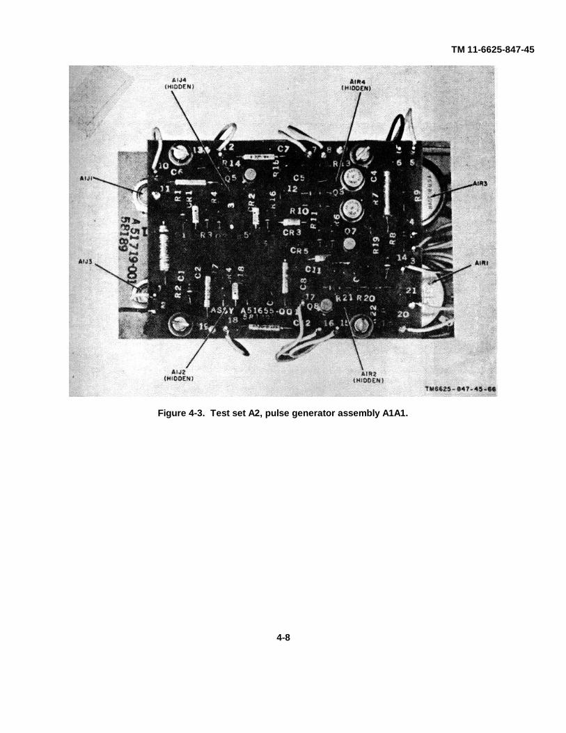
TM 11-6625-847-45
Figure 4-3. Test set A2, pulse generator assembly A1A1.
4-8
TM 11-6625-847-45
4-7. Test Set A2, Pulse Generator Assembly A1A1, Tests
a. Test Equipment and Materials.(1) Generator, Signal AN/URM-127.(2) Oscilloscope AN/USM-140(*).(3) Tee Connector UG-274B/U.(4) A test cable, fabricated as shown in figure 6-17 from materials listed in paragraph 4-2c.
b. Test Connections and Conditions. Connect the test equipment as shown in figure 6-17 to test pulse generator assembly A1A1. Pulse generatorassembly A1A1 is illustrated by figure 4-3.
c. Procedure.Step Control settingsNo. Test equipment Equipment under test Test procedure Performance standard1 AN/USM-140 Test set A2 a. Set the SERV SEL switch to a. None.
POWER switch: ON POWER switch: OFF STBY, and set the POWERINTENSITY control: PA/RT switch: PA switch on the test set to
Adjust for ease of SERV SEL switch: OFF ON. Set commonviewing. KEY switch: OFF module tray A1A2
FOCUS control: ad- XMIT STATUS: OPR POWER switch to 0N.just for a sharp ALC VOLTAGE INFO: maxclear display. Ad- ccw OFF. b. Connect the fabricated cable b. None.just other controls as ALC VOLTAGE TUNE con- to the connector of pulserequired. trol: max ccw OFF generator assembly A1A1
AN/URM-127 IF OSCILLATOR select switch: 4 from which a reading is toPOWER switch: ON MC FREQ 10MC switch: 0 be taken (outputs 1, 2,FREQ RANGE MC FREQ 1MC switch: 0 or 3).
MULTIPLIER: X1 MC FREQ .1MC switch: 0 c. Connect the AN/USM-140(*) c. None.Dial: 500 cps 500 VDC LOAD switch: LOW probe to the output of theATTENUATOR and 2400 VDC LOAD switch: 1 AN/URM-127. Verify the
OUTPJT CON- Install common presence of 500 cps at 2TROL: Adjust as module tray A1A2. volts - (Checkrequired to maintain to see that the test set is2 volts. being supplied +27 volts
dc from the PP-1451/G.)PP-1451/G d. Connect the AN/USM-140(*) d. None.
Power switch: ON probe to the output leadsof the fabricated cable con-nected to A1J4, and adjustthe AN/USM-140(*) fora single 1-µsec positivepulse.
e. Set A1R3 fully clockwise, e. A positive pulse from less thanand adjust A1R4 from 1.0 µsec to more than 1.2 µsecfully counterclockwise to (A1R4 rotated clockwise).fully clockwise
f. Adjust A1R3 from fully f. A positive pulse of less thancounterclockwise to fully 0.35 volt increasing toclockwise. more than 5 volts as A1R3.
is rotated clockwise.g. Connect the AN/USM-140(*) g. None.
and the fabricated cableto A1J3, and set A1R1to fully clockwise.
h. Adjust the AN/USM-140(*) h. None.to display a single positivepulse of approximately140-µsec duration.
i. Adjust A1R2 from fully i A positive pulse from lesscounterclockwise to fully than 70 µsec to greaterclockwise. than 210 µsec as A1R2 is
rotated clockwise.j. Adjust A1R1, from fully j. Amplitude varies from less
counterclockwise to fully than 0.1 volt to more thanclockwise. 1.3 volts
k. Connect the AN/USM-140(*) k. None.and the fabricated lead toA1J2, and adjust the AN/USM-140(*) to displayan average single pulseof 140 µsec.
l. Set A1R1 to a fully clockwise l. A negative pulse from lessposition, and adjust A1R2 than 70 µsec to more thanfrom fully counterclockwise 210 µsec as A1R2 is rotatedto fully clockwise. clockwise.
m. Adjust A1R1 fully counter- m. The amplitude varies fromclockwise to fully clock- less than 0.1 volt to morewise. than 0.8 volt
n. Turn the POWER switch n. None.on the test set and thepower switch on the PP-1451/G to OFF.
4-9
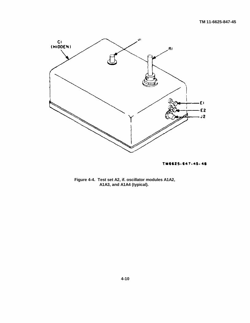
TM 11-6625-847-45
Figure 4-4. Test set A2, if. oscillator modules A1A2,A1A3, and A1A4 (typical).
4-10

TM 11-6625-847-45
4-8. Test Set A2, If. Oscillator Modules A1A2, A1A3, and A1A4 Tests
The test of each oscillator module differs only in the operating frequency of the oscillator.a. Test Equipment and Materials.
(1) Voltmeter, Electronic AN/URM-145.(2) Electronic Counter, Digital Readout AN/URM-207.(3) Fixed resistor: 51 ohms, 1/2 watt.(4) Connector UG1460/U.
b. Test Connections and Conditions. Connect the equipment as shown in Figure 6-18. Figure 4-4 illustrates the if. oscillator module controls, jacks, andtest points.
c. Procedure.Step Control settingsNo. Test equipment Equipment under test Test procedure Performance standard1 AN/URM-145 SM442A/GRC a. Set the PP-1451/G power a. None.
Power switch: ON POWER switch: OFF switch and the test setVOLTS switch: .01 SERV SEL switch: STBY POWER switch to ON
PP-1451/G PA/RT switch: PA (test set supplied 27 voltsPower switch: OFF KEY switch: OFF dc).NORMAL CHARGE XMIT STATUS switch: OPR b. Connect the AN/URM-145 b. Indication should be less
switch: NORMAL REC-XMIT switch: REC probe, in turn, to A1A2J1, than 30 mv.ALC VOLTAGE INFO control: A1A3J1, and A1A4J1.
fully counterclockwise. (For a more accurate indi-ALC VOLTAGE TUNE con- cation on the AN/URM-
trol: fully counterclockwise. 145, use a lower voltageIF OSCILLATOR SELECT range.) Change the IF
switch: 1+3 (change as re- OSCILLATOR, SELECTquired). switch setting as required.
MC FREQ 10MC switch: 0 c. Turn the three IF OSCIL- c. None.MC FREQ 1MC switch: 0 LATOR output level con-MC FREQ .1MC switch: 0 trols 1, 2, and 3 (A2R1,500 VDC LOAD switch: LOW A3R1, and A4R1) fully2400 VDC LOAD switch: 1 clockwise.IF OSCILLATORS 1, 2, and 3 d. Check to see that the AN/ d. The output voltage should
output level controls: fully URM-145 VOLTS switch be at least more than 300counterclockwise. is on the .01 range. Con- mv.
nect the probe of theAN/URM-145, in turn,to A1A2J1, A1A3J1,and A1A4J1, and recordeach reading. Change theIF OSCILLATOR selectswitch setting as required.
e. Turn the AN/URM-145 e. None.power switch off.
2 Same as above, except Same as above, except set the a. Turn the power switch on the a. None.that the AN/URM- IF OSCILLATORS level PP-1451/G and the POWER145 is not used. controls fully clockwise. switch on the test set to
AN/USM-207 Note. If signal levels are ON.SENSITIVITY switch: too low, an amplifier may be b. Attach the Cable Assembly b. The following should be
.1V required to increase the signal Radio Frequency from displayed:POWER switch: to above.1 volt rms, to provide FREQ A on the AN/USM- (1)A1A431: 1.7500 mc,TRACK adequate input to the AN/USM- 207 to A1A2J1, A1A3J1, 100 cps.DISPLAY control: 207. and AMA4J1, in turn, and (2)A1A3J1: 1.7515 mc,
Set for display time record the frequency dis- 100 cps.desired. played at each test point. (3)A1A2J1: 1.7525 mc,
100 cps.c. Refer to figures 3-10, 4-4, c. The frequency should not
and 6-3 to locate capacitor vary more than +100 cpsC1 on each if. oscillator. from the value recorded inRotate C1 on each if. oscil- b above.lator, respectively, throughits full travel, and recordthe minimum and maximumfrequencies for each if.oscillator.
d. Turn the POWER switch on d. None.the test set, the powerswitch on the PP-1451/G,and the POWER switchon the AN/USM-207 toOFF.
4-11
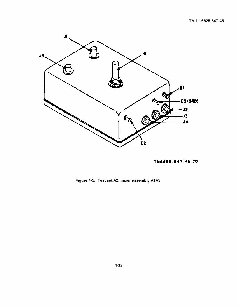
TM 11-6625-847-45
Figure 4-5. Test set A2, mixer assembly A1A5.
4-12
4-9. Test Set, Mixer Assembly A1A5, Tests
a. Test Equipment and Materials.(1) Generator, Signal AN/GRM-5D.(2) Voltmeter, Electronic AN/URM-145.(3) Four UG-1460/U connectors.(4) Tee Connect UG-274B/U.(5) Two Sealectro 5051 BNC connectors.(6) Twelve index of RG-196/U coaxial cable.(7) Two fixed resistors, 51 ohms, 1/2 watt each.(8) Two clips, electrical (alligator clips).
b. Test Connections and Conditions. Connect the test equipment, as shown in Figure 6-19, to mixer assembly A1A5 (Fig. 4-5). Fabricate the two 51-ohmtest leads (Fig. 6-19), and connect as directed in the procedure (c below).
c. Procedure.Step Control settingsNo. Test equipment Equipment under test Test procedure Performance standard1 AN/GRM-50 SM-442A/GRC
RANGE switch: POWER switch: OFF a. Connect the 51-ohm fabricated a. None.530KC-1800KC SERV SEL switch: STBY test loads (fig. 4-5 and 6-
FREQUENCY control: PA/RT switch: PA 19) to A1A5J2 and to1750.00KC KEY switch: OFF A1A5J4 on mixer assembly
MODULATION SE- XMIT STATUS switch: OPR A1A5 (fig. 3-10).LECTOR: CW REC-XMIT switch: REC b. Connect one end of cable b. None.
AN/URM-145 ALC VOLTAGE INFO con- W1 to the Tee ConnectorVOLTS switch: .3 trol: Fully counterclockwise UG-274B/U on the AN/
Power switch: ON ALC VOLTAGE TUNE con- GRM-50 to TWO TONE INtrol: Fully counterclockwise connector A1A5J1.
IF OSCILLATOR SELECT c. Set A1A5R1 fully clockwise c. None.switch: 1 and turn the PP-1451/G
IF OSCILLATORS 1, 2, and 3 power switch and the SM-output level controls: Fully 442A/GRC POWER switchcounterclockwise to ON.
MC FREQ 10MC switch: 0 d. With the AN/URM-145 con- d. NoneMC FREQ 1MC switch: 0 nected to the remaining endMC FREQ .1MC ditch: 0 of the tee connector, adjust500 VDC LOAD switch: LOW the AN/GRM-50 to 1.752400 VDC LOAD switch: 1 mc at 150 mv.
e. Connect the AN/URM-145 to e. Not less than 0.075 mv.the TWO TONE OUTconnector, and record theoutput level.
2 Same as step 1 above. Same as step 1 above. a. Connect the AN/GRM-50 a. None.to A1A5J4. Connect theAN/URM-145 to the teeconnector on the AN/GRM-50, and check to see thatthe output is 150 mv.
b. Connect one end of cable b. None.W1 to the tee connectoron the AN/GRM-50 toTWO TONE IN connectorA1A5J1.
c. Connect one of the 51-ohm c. None.fabricated test leads toA1A5J3, and set A1A5R1fully counterclockwise.
d. Connect the AN/URM-145 d. Less than 1-mv output.to A1A5J5, and measurethe output (use 0.003range).
e. Set A1A5R1 fully clockwise......... e. More than 10-mv output.f. Remove the 51-ohm test load f. None
from A1A5J3, connect itto A1A5J4, and set A1A5R1fully counterclockwise.
g. Feed the 150-mv signal into g. Less than 1-mv output.A1A5J1.
h. Set A1A5R1 fully clockwise......... h. More than 10-mv output.i. Turn the power switches to
OFF.
4-13
TM 11-6625-847-45
Figure 4-6. Common module tray A1A2 if. amplifier module A1.
4-14
TM 11-6625-847-45
4-10. Common Module Army A1A2 If. Amplifier Module A1 Testsa. Test Equipment and Materials.
(1) Voltmeter, Electronic AN/URM-145.(2) Generator, Signal AN/GRM-50.(3) Potentiometer, 10-kilohms, 2 watts.(4) The test set ±20-volt dc supply.
b. Test Connections and Conditions. Connect the test equipment as shown in figure 6-20 to if. amplifier module A1.(To remove if. amplifier module A1 from tray A1A2, refer to paragraph 8-43 and figure 3-20. The fast points are shownon figure 4-6.
c. Procedure.
Step Control settingsNo. Test equipment Equipment under test Test procedure
1 AN/URM-145 SM-442A/GRC a. Connect a ground lead be- a. None.VOLTS switch: .003 POWER switch: OFF tween test set connectorPower switch: ON Tray A1A2 J1, pin 70, and pin 70 of
AN/GRM-50 POWER switch: OFF J1 on tray A1A2.,RANGE switch: SQUELCH switch: OFF b. Connect a lead between pin b. None.
530 kc to 1,801 kc SQUELCH SYNC switch: OFF 41 of J1 on the test set andFREQUENCY con- AUDIO GAIN control: Fully pin 41 of J1 on tray A1A4
trol: 1750.00 counterclockwise Note. If test is made withMODULATION SE- AGC SYNC switch: OFF A1A2A1 out of tray A1A2, con-
LECTOR: CW RF AGC ON OFF switch: OFF nect the ground lead toPOWER switch: ON TEST SELECTOR switch: 1 A1A2A1E8, and the +20-volt
PP-1451/G BFO TONE control: Fully coun- dc lead to A1A2A1E11.NORMAL CHARGE terclockwise c. TURN the test set POWER c. None.
switch: NORMAL RF GAIN control: Fully coun- switch and the tray A1A2Power switch: ON terclockwise power switch to ON.
ALC APC CONTROL ALC d. Connect the AN/URM-145 d. None.switch: OFF probe to terminal A1E2,
ALC APC PPC CONTROL and the probe clip to ter-POWER control: Fully coun- minal A1E3. Adjust theterclockwise AN/GRM-50 for an out-
ALC APC PPC CONTROL put at 1.75 meat 1 ± 0.1APC/PPC SEL switch: OFF mv rms.
VOICE MODES switch: e. Remove the AN/URM-145 e. None.PUSH TO TALK probe loads from A1E2
TEST SELECTOR switch: 1 and A1E3, and connect theNote. If A1A2A1 is tested probe to terminal A1E14
separately from tray A1A2, the and the probe clip lead toabove control settings need not terminal A1E15.be made on tray A1A2. f. Adjust the 10-kilohm, 2-watt f. Output is 25 mv, or approxi-
potentiometer for maxi- mately 20 dbmum output on the AN/URM-146.
g. Turn the POWER switchesOFF, and disconnect the g. None.equipment.
4-15
TM 11-6625-847-45
Figure 4-7. Synthesizer test tray A1A3, amplifier modules AR1 through AR5.
4-16

TM 11-6625-847-45
4-11. Synthesizer Test Tray A1A3, Amplifier Modules AR1 through AR5 TestsThe tests of amplifier modules AR1 through AR5 are the same for each module; however, the test results, step 2, for AR3 are different. To remove and replacethe modules for the individual bench testing, refer to paragraphs 3-49 and 3-51c.
a. Test Equipment and Materials.(1) Generator, Signal AN/GRM-50.(2) Voltmeter, Electronic AN/URM-145.(3) Test set A2 20-volt dc supply.(4) Tee Connector UG-274B/U.(5) Two Connectors UG-88C/U and two Sealectro 5051 connectors.(6) Two Connectors UG-1460/U.
b. Test Connectors and Conditions. Connect the test equipment, as shown in figure 6-21, to amplifier modules AR1 through AR5 (fig. 4-7) to be tested.c. Procedure.
Step Control settingsNo. Test equipment Equipment under test Test procedure Performance standard1 PP-1451/G Test set A2 a. Turn the PP-1451/G power a. None.
NORMAL-CHARGE POWER switch: OFF switch to ON. Turn theswitch: NORMAL Tray A1A3 test set POWER switch to
Power switch: OFF Power switch: OFF ON. Turn the FREQVOLTAGE ADJUST MODULE SELECT switch: STANDARD OUTPUT
control: Set for 10 and 1 KC AMPL SWITCH to OFF.27-volt dc on OUT- POWER VAR-FINED switch: Set tray A1A3 power switchPUT VOLTAGE FIXED to ON. Turn the FREQmeter ADJ control: Midrange STANDARD OUTPUT
AN/GRM-50 FREQ SFLECT: VOLT ADJ control fullyRANGE switch: 10 KC control: 0 counterclockwise.
530KC-1800 KC 1 KC control: 0 b. Connect the AN/URM-145 b. None.FREQUENCY con- 100 KC control: 0 probe to the W1 cable
trol: 1000KC 10 & 1 KC SYNTH: on the AN/GRM-50,POWER switch: ON SYNTH OUTPUTS AMPL Adjust the AN/GRM-50VERNIER ATTENU- ON-OFF switch: OFF for a 1,000-kc output at
ATOR switch: SYNTH OUTPUTS VOLT 50 mv.AN/URM-145 ADJ control: Midrange c. Disconnect the AN/URM-145 c. Not less than 45 mv.
Power switch: ON OUTPUT AMPL ON-OFF probe from the AN/GRM-VOLTS switch: .1 switch: OFF 50 (cable W1), and con-
OUTPUT VOLT ADJ con- nect it to the lead attached totroI: Midrange A1A3A1J3. Observe the
FREQ DIVIDER FREQ voltage level on the AN/SHIFT switch: OFF URM-145.
FREQ STANDARD: d. Set the amplifier module d Less than 40 mv.OUTPUT AMPL ON-OFF A1 FREQ STANDARD
switch (2): OFF OUTPUT AMPL switchOUTPUT VOLT ADJ con- to ON. Record the reading
trol (2): Midrange on AN/URM-145.MC SYNTH section:
OUTPUT AMPL ON-OFFswitch: OFF
OUTPUT VOIT ADJ con-trol: Midrange
e. Rotate the amplifier module e. At least 100 mv.A1 FREQ STANDARDOUTPUT VOLT ADJcontrol fully clockwise,and observe the indicationan the AN/URM-145.
f. Repeat the procedures in a f. None.through e above with inputfrequencies of 7.1, 10,and 23.5 mc.
2 Same as step 1 above 1 Same as step 1 above. a. Check to see that equipment a. None.except set the VOLTS is set up, connected, andswitch on the AN/ turned on in the sameURM-145 to 1. manner as in step 1 above.
b. Set the amplifier module A1 b. None.FREQ STANDARDOUTPUT AMPL switch toOFF, and the amplifiermodule A1 FREQ STAND-ARD OUTPUT VOLTADJ control fully coun-terclockwise.
c. Connect the AN/URM-145 c. None.probe to cable W1 on theAN/GRM-50, and adjustthe AN/GRM-50 for anoutput of 1 mc at 560 ± 100mv. Record this reading.
d. Connect the AN/URM-145 d. Not less than 5 mv of theprobe to the lead attached level recorded in c above.to A1A3A1J3. Observeand record the voltagelevel on the AN/URM-145.
e. Set the FREQ STANDARD e. Less than 460 mv.OUTPUT AMPL switchto ON. Observe the indi-cation an AN/URM-145.
f. Rotate the FREQ STANDARD f. More than 660 mv.OUTPUT VOLT ADJ con-trol fully clockwise.
g. Turn the power switch onthe PP-1451/G to OFF,and disconnect the testequipment.
4-17
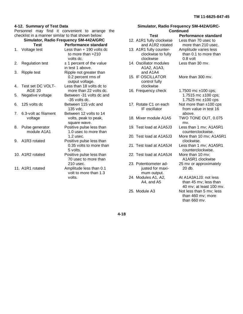
TM 11-6625-847-45
4-12. Summary of Test DataPersonnel may find it convenient to arrange thechecklist in a manner similar to that shown below:
Simulator, Radio Frequency SM-442A/GRCTest Performance standard
1. Voltage test Less than + 190 volts dcto more than +210volts dc.
2. Regulation test ± 1 percent of the valuein test 1 above.
3. Ripple test Ripple not greater than0.2 percent rms ofoutput voltage.
4. Test set DC VOLT- Less than 18 volts dc toAGE 20 more than 22 volts dc.
5. Negative voltage Between -31 volts dc and-35 volts dc.
6. 125 volts dc Between 115 vdc and135 vdc.
7. 6.3-volt ac filament Between 12 volts to 14voltage volts, peak to peak,
square wave.8. Pulse generator Positive pulse less than
module A1A1 1.0 usec to more than1.2 usec.
9. A1R3 rotated Positive pulse less than0.35 volts to more than5 volts.
10. A1R2 rotated Positive pulse less than70 usec to more than210 usec.
11. A1R1 rotated Amplitude less than 0.1volt to more than 1.3volts.
Simulator, Radio Frequency SM-442A/GRC-Continued
Test Performance standard12. A1R1 fully clockwise Less than 70 usec to
and A1R2 rotated more than 210 usec.13. A1R1 fully counter- Amplitude varies less
clockwise to fully than 0.1 to more thanclockwise 0.8 volt
14. Oscillator modules Less than 30 mv.A1A2, A1A3,and A1A4
15. IF OSCILLATOR More than 300 mv.control fullyclockwise
16. Frequency check 1.7500 mc ±100 cps;1.7515 mc ±100 cps;1.7525 mc ±100 cps
17. Rotate C1 on each Not more than ±100 cpsIF oscillator from value in test 16
above.18. Mixer module A1A5 TWO TONE OUT, 0.075
mv.19. Test load at A1A5J3 Less than 1 mv; A1A5R1
counterclockwise.20. Test load at A1A5J3 More than 10 mv; A1A5R1
clockwise.21. Test load at A1A5J4 Less than 1 mv; A1A5R1
counterclockwise.22. Test load at A1A5J4 More than 10 mv;
A1A5R1 clockwise23. Potentiometer ad- 25 mv or approximately
justed for maxi- 20 db.mum output.
24. Modules A1, A2, At A1A3A1J3: not lessA4, and A5 than 45 mv; less than
40 mv; at least 100 mv.25. Module A3 Not less than 5 mv; less
than 460 mv; morethan 660 mv.
4-18
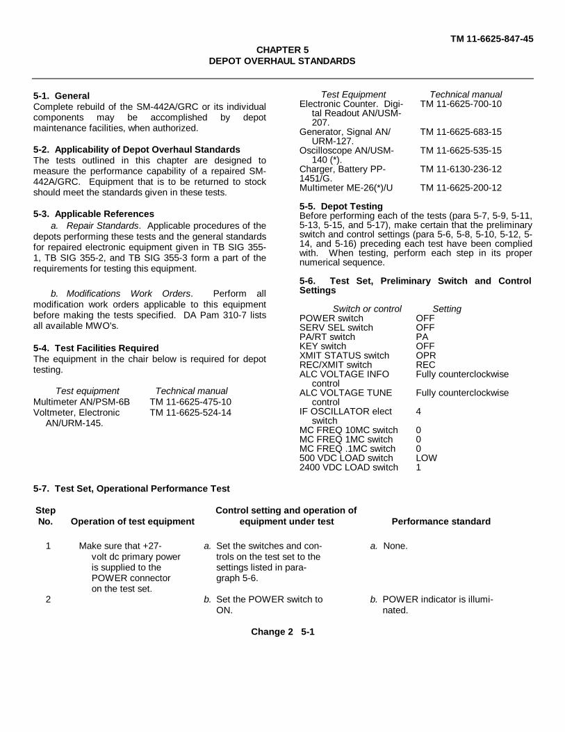
TM 11-6625-847-45CHAPTER 5
DEPOT OVERHAUL STANDARDS
5-1. GeneralComplete rebuild of the SM-442A/GRC or its individualcomponents may be accomplished by depotmaintenance facilities, when authorized.
5-2. Applicability of Depot Overhaul StandardsThe tests outlined in this chapter are designed tomeasure the performance capability of a repaired SM-442A/GRC. Equipment that is to be returned to stockshould meet the standards given in these tests.
5-3. Applicable Referencesa. Repair Standards. Applicable procedures of the
depots performing these tests and the general standardsfor repaired electronic equipment given in TB SIG 355-1, TB SIG 355-2, and TB SIG 355-3 form a part of therequirements for testing this equipment.
b. Modifications Work Orders. Perform allmodification work orders applicable to this equipmentbefore making the tests specified. DA Pam 310-7 listsall available MWO's.
5-4. Test Facilities RequiredThe equipment in the chair below is required for depottesting.
Test equipment Technical manualMultimeter AN/PSM-6B TM 11-6625-475-10Voltmeter, Electronic TM 11-6625-524-14
AN/URM-145.
Test Equipment Technical manualElectronic Counter. Digi- TM 11-6625-700-10
tal Readout AN/USM-207.
Generator, Signal AN/ TM 11-6625-683-15URM-127.
Oscilloscope AN/USM- TM 11-6625-535-15140 (*).
Charger, Battery PP- TM 11-6130-236-121451/G.MuItimeter ME-26(*)/U TM 11-6625-200-12
5-5. Depot TestingBefore performing each of the tests (para 5-7, 5-9, 5-11,5-13, 5-15, and 5-17), make certain that the preliminaryswitch and control settings (para 5-6, 5-8, 5-10, 5-12, 5-14, and 5-16) preceding each test have been compliedwith. When testing, perform each step in its propernumerical sequence.
5-6. Test Set, Preliminary Switch and ControlSettings
Switch or control SettingPOWER switch OFFSERV SEL switch OFFPA/RT switch PAKEY switch OFFXMIT STATUS switch OPRREC/XMIT switch RECALC VOLTAGE INFO Fully counterclockwise
controlALC VOLTAGE TUNE Fully counterclockwise
controlIF OSCILLATOR elect 4
switchMC FREQ 10MC switch 0MC FREQ 1MC switch 0MC FREQ .1MC switch 0500 VDC LOAD switch LOW2400 VDC LOAD switch 1
5-7. Test Set, Operational Performance Test
Step Control setting and operation ofNo. Operation of test equipment equipment under test Performance standard
1 Make sure that +27- a. Set the switches and con- a. None.volt dc primary power trols on the test set to theis supplied to the settings listed in para-POWER connector graph 5-6.on the test set.
2 b. Set the POWER switch to b. POWER indicator is illumi-ON. nated.
Change 2 5-1
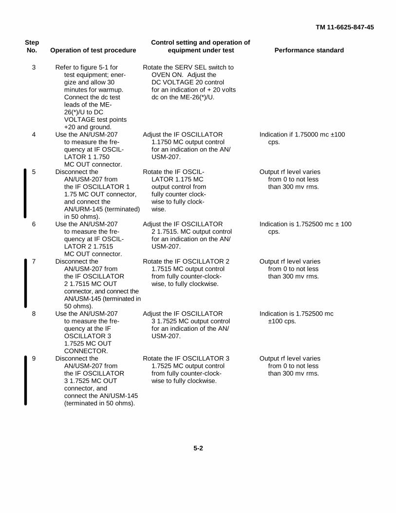
TM 11-6625-847-45
Step Control setting and operation ofNo. Operation of test procedure equipment under test Performance standard
3 Refer to figure 5-1 for Rotate the SERV SEL switch totest equipment; ener- OVEN ON. Adjust thegize and allow 30 DC VOLTAGE 20 controlminutes for warmup. for an indication of + 20 voltsConnect the dc test dc on the ME-26(*)/U.leads of the ME-26(*)/U to DCVOLTAGE test points+20 and ground.
4 Use the AN/USM-207 Adjust the IF OSCILLATOR Indication if 1.75000 mc ±100to measure the fre- 1.1750 MC output control cps.quency at IF OSCIL- for an indication on the AN/LATOR 1 1.750 USM-207.MC OUT connector.
5 Disconnect the Rotate the IF OSCIL- Output rf level variesAN/USM-207 from LATOR 1.175 MC from 0 to not lessthe IF OSCILLATOR 1 output control from than 300 mv rms.1.75 MC OUT connector, fully counter clock-and connect the wise to fully clock-AN/URM-145 (terminated) wise.in 50 ohms).
6 Use the AN/USM-207 Adjust the IF OSCILLATOR Indication is 1.752500 mc ± 100to measure the fre- 2 1.7515. MC output control cps.quency at IF OSCIL- for an indication on the AN/LATOR 2 1.7515 USM-207.MC OUT connector.
7 Disconnect the Rotate the IF OSCILLATOR 2 Output rf level variesAN/USM-207 from 1.7515 MC output control from 0 to not lessthe IF OSCILLATOR from fully counter-clock- than 300 mv rms.2 1.7515 MC OUT wise, to fully clockwise.connector, and connect theAN/USM-145 (terminated in50 ohms).
8 Use the AN/USM-207 Adjust the IF OSCILLATOR Indication is 1.752500 mcto measure the fre- 3 1.7525 MC output control ±100 cps.quency at the IF for an indication of the AN/OSCILLATOR 3 USM-207.1.7525 MC OUTCONNECTOR.
9 Disconnect the Rotate the IF OSCILLATOR 3 Output rf level variesAN/USM-207 from 1.7525 MC output control from 0 to not lessthe IF OSCILLATOR from fully counter-clock- than 300 mv rms.3 1.7525 MC OUT wise to fully clockwise.connector, andconnect the AN/USM-145(terminated in 50 ohms).
5-2
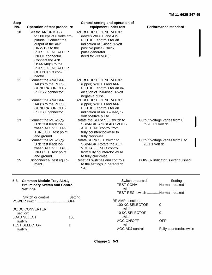
TM 11-6625-847-45
Step Control setting and operation ofNo. Operation of test procedure equipment under test Performance standard
10 Set the AN/URM-127 Adjust PULSE GENERATORto 500 cps at 6 volts am- (lower) WIDTH and AM-plitude. Connect the PLITUDE controls for anoutput of the AN/ indication of 1-usec, 1-voltURM-127 to the positive pulse (CheckPULSE GENERATOR pulse generatorINPUT connector. need for -33 VDC).Connect the AN/USM-140(*) to thePULSE GENERATOROUTPUTS 3 con-nector.
11 Connect the AN/USM- Adjust PULSE GENERATOR140(*) to the PULSE (upper) WIDTH and AM-GENERATOR OUT- PLITUDE controls for an in-PUTS 2 connector. dication of 150-usec, 1-volt
negative pulse.12 Connect the AN/USM- Adjust PULSE GENERATOR
140(*) to the PULSE (upper) WIDTH and AM-GENERATOR OUT- PLITUDE controls for anPUTS 1 connector. indication of an 85-usec, 1-
volt positive pulse.13 Connect the ME-26(*)/ Rotate the SERV SEL switch to Output voltage varies from 0
U dc test leads be- SSB/NSK. Adjust ALC VOLT- to 20 ± 1 volt dc.tween ALC VOLTAGE AGE TUNE control fromTUNE OUT test point fully counterclockwise toand ground. fully clockwise.
14 Connect the ME-26(*)/ Rotate SERV SEL switch to Output voltage varies from 0 toU dc test leads be- SSB/NSK. Rotate the ALC 20 ± 1 volt dc.tween ALC VOLTAGE VOLTAGE INFO controlINFO OUT test point from fully counterclockwiseand ground. to fully clockwise
15 Disconnect all test equip- Reset all switches and controls POWER indicator is extinguished.ment. to the settings in paragraph
5-6.
5-8. Common Module Tray A1A1,Preliminary Switch and ControlSettings
Switch or control SettingPOWER switch ...............................OFF
DC/DC CONVERTERsection:
LOAD SELECT 100switch.
TEST SELECTOR 1switch.
Switch or control SettingTEST CONV Normal, relaxed
switchTEST REG switch ............Normal, relaxed
RF AMPL section:100 KC SELECTOR 0
switch.10 KC SELECTOR 0
switch.AGC ON/OFF OFF
switch.AGC ADJ control Fully counterclockwise
Change 1 5-3
TM 11-6625-847-45
Figure 5-1. Test set operational performance test setup.
5-9. Common Module Tray A1A1, Operational Performance TestNote. The ME-26(*)/U is the only piece of test equipment required for this test.
Step Control setting and operation ofNo. Operation of test procedure equipment under test Performance standard
1 Remove common module trayA1A1 from case 2, and se-cure it to the test set.
2 Make sure that +27- Set the switches and controlsvolt dc primary on the test set to the positionspower is supplied to listed in paragraph 5-6. Setthe POWER connec- the switches and controls onter on the test set. common module tray A1A1
to the settings listed in par-graph 5-8.
3 Set the POWER switch on the POWER indicator on test settest set to ON. Set the POWER is illuminatedswitch on common module trayA1A1 to ON.
4 Measure the dc voltage Rotate the SERV SEL switch Measured is +27 ± 1at DC/DC CONVER- on the test set to SSB/NSK. dc; POWER indicator onTER test points HI common module tray A1A1and LOW on tray is illuminated.A1A1 using the ME-26(*)/U.
5-4

TM 11-6625-847-45Step Control setting and operation ofNo. Operation of test procedure equipment under test Performance standard
5 Connect the dc test Set the AGC OFF/ON switch Measured voltageleads of the on tray A1A1 to ON. varies from 0ME-26(*)/U to AGC Rotate the AGC ADJ con- to -33 ±2 voltstest points TEST trol from fully counter- dc.and ground on tray A1A1. clockwise to fully clockwise.
6 Measure the dc voltage Measure voltage is + 20 ± 1at NOISE BLANKER volts dc.20 VDC test point ontray A1A1 using ME-26(*)/U.
7 Rotate the MC FREQ 10MC Mc shaft coupler on tray A1A1and 1MC frequency select rotates, indicating the 28 posi-switches 01 the test set from tions selected.2.0 mc to 29.0 mc in 1-mcsteps.
8 Disconnect the ME- Reset all switches and controls POWER indicators on the test26(*)/U. to the settings, listed in para- set and common module tray
graphs 5-6 and 5-8. A1A1 are extinguished.
5-10. Common Module Tray A1A2, Preliminary Switch and Control Settings
Switch or control Setting Switch or control SettingPOWER switch .................... OFF RF GAIN control ................Fully counterclockwiseRCVR AUDIO section: XMTR IF AND AUDIO
SQUELCH switch ............ OFF section:SQUELCH SYNC OFF ALC APC PPCswitch. CONTROL:AUDIO GAIN con- Fully counterclockwise ALC switch....................OFFtrol. ALC/PPC SEL OFF
RCVR IF section: switch.AGC SYNC switch........... OFF POWER CON- Fully counterclockwiseRF-AGC ON/OFF OFF TROL.switch. CE MODES PUSH TO TALK
TEST SELECTOR 1 switch.switch. TEST SELECTOR 1
BFO TONE control............... Fully counterclockwise switch.
5-11. Common Module Tray A1A2, Operational Performance TestStep Control setting and operation ofNo. Operation of test procedure equipment under test Performance standard1 Remove common on module tray
A1A2 from the case 2, andsecure it to the test set.
2 Make sure that +27- Set the switches and controls onvolt dc primarily power the test set to the settingsis supplied to the listed in paragraph 5-6. SetPOWER connector the switches and controls onon the test set. common module tray A1A2
to the settings listed in para-graph 5-10.
3 Set the POWER switch on the POWER indicator is illuminatedtest set to ON. on the test set.
Change 2 5-5
TM 11-6625-847-45Step Control setting and operation ofNo. Operation of test procedure equipment under test Performance standard4 NOTE Allow a 10- Rotate the SERV SEL. POWER indicator on common
minute, warmup period switch on the test set to SSB/ module tray A1A2 illuminated.for test set frequency NSK. Set. the POWER switchstandard. on common module tray
A1A2 to ON.5 Connect the dc test leads Voltage measures 33 ± 2
of the ME-26(*)/U to volts dc.RCVR IF test pointsHl and LO on trayA1A2.
6 Set the RCVR IF TEST SE- Dc voltage varies from notLECTOR switch on tray more than 0.35 to notless than 2.5 volts dc. less than 2.5 volts dc.Rotate the RCVR IF RFGAIN control from fullycounterclockwise.
7 Check the dc voltage Switch the REC XMIT Dc voltage drops to 0 whenindication on the ME- switch oil this test set REC XMIT switch is set to26(*)/U when the from REC to XMIT, XMIT.REC XMIT switch on then back to REC.the test set is set toXMIT.
8 ON tray A1A2, set the RCVR Indication is + 20 ± 1 volts dcIF TEST SELECTOR switch (BFO TONE control hasto position 3. Rotate the SERV effect on the voltage).SEL switch on the test setto CW. Rotate the RCVR IFBFO TONE control on trayA1A2 from fully clockwiseclockwise to fully clockwise.
9 Connect the AN/USM-207 to Set the AGC SYNC switch on Measurement is 1.7515 mcthe TWO TONE OUT tray A1A2 to ON. Set ± 100 cps.connector on the test set; the test set IF OSCILLATORrefer to figure 5-1. select switch to 1 +2.
10 Set the test set IF OSCILLATOR Measurement is 1.7525 rncselect switch to 1 +3. ± 100 cps.
11 Measure the dc voltage Voltage measures + 20 ± 1 voltat XMTR IF AND dc.AUDIO test pointsHI and LO on trayA1A2.
12 Set the XMTR IF AND AUDIO Dc voltage varies from a mini-TEST SELECTOR switch on mum of 0 volt dc to a maxi-tray A1A2 to 3, find the test mum of + 20 volts dc.set KEY switch to ON. Rotatethe XMTR IF AND AUDIOALC APC PPC POWERCONTROL on tray A1A2 fromfully clockwise to fullycounterclockwise.
18 Disconnect all test equip- Reset all switches and controls to POWER indicators on the testment. the setting listed in paragraphs set and tray A1A2 are ex-
5-6 and 5-10. tinguished.
5-6
TM 11-6625-847-45
Figure 5-2. Synthesizer test tray A1A3, operative performance test, test equipment.
5-12. Synthesizer Test Tray A1A3,Preliminary Switch and ControlSettings
Switch or control SettingPOWER switch ......................OFFMODULE SELECT switch 10 & 1KCPOWER section:
VAR/FIXED switch ...........FIXEDADJ control ......................Midrange
FREQ SELECT section:10KC control ....................01KC control......................0100 KC control .................0
10&1KC SYNTHsection:SYNTH OUTPUTS OFF
AMPL switch.SYNTH OUTPUTS Midrange
VOLTS ADJ con-trol.
Switch or control SettingOUTPUT AMPL OFF
switch.OUTPUT VOLT ADJ Midrange
control.FREQ DIVIDER sec-
tion:FREQ SHIFT switch ........ OFF
FREQ STANDARDsection:OUTPUT AMPL switch OFF
(both switches).OUTPUT VOLT ADJ Midrange
control (both con-trols).
MC SYNTH section:OUTPUT AMPL switch .... OFFOUTPUT VOLT Midrange
ADJ control.
5-7
TM 11-6625-847-45
5-13. Synthesizer Test Tray A1A3, Operational Performance Test
Step Control setting and operation ofNo. Operation of test procedure equipment under test Performance standard1 Make sure that +27-volt On the test set, set switches and
dc primary power is controls to the settings listedsupplied to the POWER in paragraph 5-6.connector on the test set.
2 Remove synthesizer test trayA1A3 from case, and installit in the test set.
3 On synthesizer test tray A1A3,set switches and controls to thesetting listed in paragraph 5-12.
4 On the test set, set the POWER Test met POWER indicator il-switch to ON; set the SERV luminated.SEL switch to STBY.
5 On synthesizer test tray A1A3, Synthesizer test tray A1A3 POWERset the POWER switch to ON. indicator is illuminated
6 On the test set, rotate the MC On synthesizer test tray A1A3,FREQ 10MC and 1MC switches MC SYNTH module couplerfrom 2 mc to 29 mc in 1-mc is adjusted to a now setting eachsteps. Check module coupler time the MC FREQ 10MC and 1in MC SYNTH section on switches are adjusted.synthesizer test tray A3.
7 On synthesizer test tray A1A3, On synthesizer test tray A1A3,set the POWER switch to OFF. POWER indicator is extin-On the test et, set the SERV guished.SEL itch to OFF.
8 Connect the test equip-ment as indicated infigure 5-2, and applyoperating power tothe test equipment.Secure the followingRT-662/GRC modules,and install then in theirappropriate connectorson synthesizer testtray A1A3 (checkcoupler alignments):
a. Module 1A2, 100-kcsynthesizer.
b. Module 1A3, frequencystandard.
c. Module 1A4, 10- and1-kc synthesizer.
d. Module 1A6, frequencydivider.
e. Module 1A8, transistor.f. Module 1A9, mc syn-
thesizer.9 On the test set, set the SERV On synthesizer test tray A1A3,
SEL switch to STBY. On syn- POWER indicator is illuminated.thesizer test tray A1A3, setthe POWER switch to ON.
10 If operating from a cold start,allow 15 minutes warmup timefor equipment stability. Ifequipment has been warmedup within the last hour, 5 minuteswarmup time in sufficient.
5-8

TM 11-6625-847-45Step Control setting and operation ofNo. Operation of test procedure equipment under test Performance standard
11 Connect the ME-26(*)/U On synthesizer-test tray A1A3, The ME-26(*)/U indicates volt-across the POWER adjust the POWER ADJ con- age varying from a minimumINPUT VAR and ground trol from fully counterclock- of 0 volt dc to a maximumtest points on synthe- wise to fully clockwise. of + 27 volts dc; set to + 20sizer test tray A1A3. Place VAR/FIXED volts dc.
switch to VAR position.12 Disconnect the ME-26(*)/
U from the POWER IN-PUT test points.
13 Connect the AN/URM- In OUTPUT portion of 10 & Output increases as adjustment is145 to the 7.1 MC con- 1KC SYNTH section on syn- made clockwise.nector in OUTPUT thesizer, test tray A1A1, setportion of 10 & 1 KC the AMPL switch to ON andSYNTH section on adjust the VOLT ADJ controlsynthesizer test tray from fully counter-clockwise toA1A3. fully clockwise. Return the
CAUTION VOLT ADJ control to midrange.Adjust AN/URM-145 scale above1 volt and readjust accordingly toavoid damage to the instrument.
14 Disconnect the AN/URM-145 from the 7.1 MCconnector.
15 Connect the AN/URM- In SYNTH OUTPUT portion Check to see that the output145 to the 10 & 1 KC of 10 & 1 KC SYNTH section increases as the adjustment isconnector in the SYNTH on synthesizer test tray A1A3, made clockwise.OUTPUT portion of Set the AMPL switch to ONthe 10 & 1 KC SYNTH and adjust the VOLT ADJsection on synthesizer control from fully counter-test tray A1A3. clockwise to fully clockwise.
CAUTION Return the VOLT ADJ con-Adjust the AN/URM-145 to scale trol to midrange.above 1 volt, and readjust accor-dingly to avoid damage to theinstrument.
16 Disconnect the AN/URM-145 from the 10 & 1 KCconnector.
17 Connect the AN/URM- In the 10 MC OUTPUT position Output increases as adjustment145 to the 10 MC OUT on the FREQ STANDARD sec- is made clockwise.PUT connector in the tion on synthesizer test trayFREQ STANDARD A1A3, set the AMPL, switchsection on synthesizers to ON and adjust the VOLTtest tray A1A3. ADJ control from fully counter-
CAUTION clockwise to fully clockwise.Adjust AN/URM-145 to scale Return the VOLT ADJ controlabove 1 volt and readjust accord- to midrange.ingly to avoid damage to theinstrument.
18 Disconnect the AN/URM-145 from the 10 MCconnector.
19 Connect the AN/URM- In the 1 MC OUTPUT section of Output increases as adjustment145 to the 1 MC OUT- the FREQ STANDARD see- is made clockwise.PUT connector in the tion in synthesizer test trayFREQ STANDARD A1A3, set the AMPL, switch tosection on synthesizer ON and adjust the VOLT ADJtest tray A1A3. control firm fully counterclock-
5-9
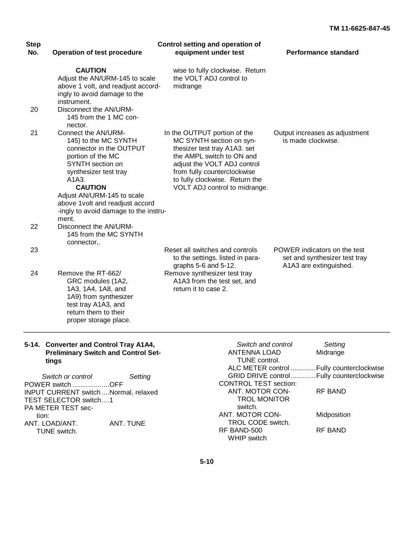
TM 11-6625-847-45
Step Control setting and operation ofNo. Operation of test procedure equipment under test Performance standard
CAUTION wise to fully clockwise. ReturnAdjust the AN/URM-145 to scale the VOLT ADJ control toabove 1 volt, and readjust accord- midrangeingly to avoid damage to theinstrument.
20 Disconnect the AN/URM-145 from the 1 MC con-nector.
21 Connect the AN/URM- In the OUTPUT portion of the Output increases as adjustment145) to the MC SYNTH MC SYNTH section on syn- is made clockwise.connector in the OUTPUT thesizer test tray A1A3. setportion of the MC the AMPL switch to ON andSYNTH section on adjust the VOLT ADJ controlsynthesizer test tray from fully counterclockwiseA1A3. to fully clockwise. Return the
CAUTION VOLT ADJ control to midrange.Adjust AN/URM-145 to scaleabove 1volt and readjust accord-ingly to avoid damage to the instru-ment.
22 Disconnect the AN/URM-145 from the MC SYNTHconnector,.
23 Reset all switches and controls POWER indicators on the testto the settings. listed in para- set and synthesizer test traygraphs 5-6 and 5-12. A1A3 are extinguished.
24 Remove the RT-662/ Remove synthesizer test trayGRC modules (1A2, A1A3 from the test set, and1A3, 1A4, 1A8, and return it to case 2.1A9) from synthesizertest tray A1A3, andreturn them to theirproper storage place.
5-14. Converter and Control Tray A1A4,Preliminary Switch and Control Set-tings
Switch or control SettingPOWER switch ...................OFFINPUT CURRENT switch ....Normal, relaxedTEST SELECTOR switch....1PA METER TEST sec-
tion:ANT. LOAD/ANT. ANT. TUNE
TUNE switch.
Switch and control SettingANTENNA LOAD Midrange
TUNE control.ALC METER control .............Fully counterclockwiseGRID DRIVE control.............Fully counterclockwise
CONTROL TEST section:ANT. MOTOR CON- RF BAND
TROL MONITORswitch.
ANT. MOTOR CON- MidpositionTROL CODE switch.
RF BAND-500 RF BANDWHIP switch
5-10
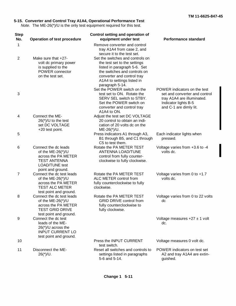
TM 11-6625-847-455-15. Converter and Control Tray A1A4, Operational Performance Test
Note. The ME-26(*)/U is the only test equipment required for this test.
Step Control setting and operation ofNo. Operation of test procedure equipment under test Performance standard1 Remove converter and control
tray A1A4 from case 2, andsecure it to the test set.
2 Make sure that +27- Set the switches and controls onvolt dc primary power the test set to the settingsis supplied to the listed in paragraph 5-6. SetPOWER connector the switches and controls onon the test set. converter and control tray
A1A4 to settings listed inparagraph 5-14.
Set the POWER switch on the POWER indicators on the test3 test set to ON. Rotate the set and converter and control
SERV SEL switch to STBY. tray A1A4 are illuminated.Set the POWER switch on Indicator lights B-5converter and control tray and C-1 are dimly lit.A1A4 to ON.
4 Connect the ME- Adjust the test set DC VOLTAGE26(*)/U to the test 20 control to obtain an indi-set DC VOLTAGE cation of 20 volts dc on the+20 test point. ME-26(*)/U.
5 Press indicators A1 through A3, Each indicator lights whenB1 through B5, and C1 through pressed.C5 to test them.
6 Connect the dc leads Rotate the PA METER TEST Voltage varies from +3.6 to -4of the ME-26(*)/U ANTENNA LOAD/TUNE volts dc.across the PA METER control from fully counter-TEST ANTENNA clockwise to fully clockwise.LOAD/TUNE testpoint and ground.
7 Connect the dc test leads Rotate the PA METER TEST Voltage varies from 0 to +1.7of the ME-26(*)/U ALC METER control from volts dc.across the PA METER fully counterclockwise to fullyTEST ALC METER clockwise.test point and ground.
8 Connect the dc test leads Rotate the PA METER TEST Voltage varies from 0 to 22 voltsof the ME-26(*)/U GRID DRIVE control from dcacross the PA METER fully counterclockwise toTEST GRID DRIVE fully clockwise.test point and ground.
9 Connect the dc test Voltage measures +27 ± 1 voltleads of the ME- dc.26(*)/U across theINPUT CURRENT LOtest point and ground.
10 Press the INPUT CURRENT Voltage measures 0 volt dc.test switch.
11 Disconnect the ME- Reset all switches and controls to POWER indicators on test set26(*)/U. settings listed in paragraphs A2 and tray A1A4 are extin-
5-6 and 5-14. guished.
Change 1 5-11
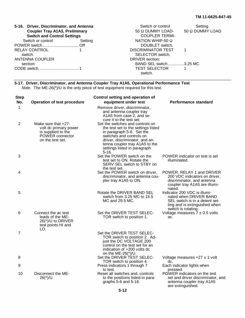
TM 11-6625-847-45
5-16. Driver, Discriminator, and AntennaCoupler Tray A1A3, PreliminarySwitch and Control Settings
Switch or control SettingPOWER switch ............................... OffRELAY CONTROL 1
switch.ANTENNA COUPLER
section:CODE switch................................... 1
Switch or control Setting50 Ω DUMMY LOAD- 50 Ω DUMMY LOAD
COUPLER TERMI-NATION WHIP-50 Ω
DOUBLET switch.DISCRIMINATOR TEST 1
SELECTOR switch.DRIVER section:
BAND SEL switch..............3.25 MCTEST SELECTOR 1
switch.
5-17. Driver, Discriminator, and Antenna Coupler Tray A1A5, Operational Performance TestNote. The ME-26(*)/U is the only piece of test equipment required for this test.
Step Control setting and operation ofNo. Operation of test procedure equipment under test Performance standard1 Remove driver, discriminator,
and antenna coupler trayA1A5 from case 2, and se-cure it to the test set.
2 Make sure that +27- Set the switches and controls onvolt dc primary power the test set to the settings listedis supplied to the in paragraph 5-6. Set thePOWER connector switches and controls onon the test set. driver, discriminator, and an-
tenna coupler tray A1A5 to thesettings listed in paragraph5-16.
3 Set the POWER switch on the POWER indicator on test is settest set to ON. Rotate the illuminated.SERV SEL switch to STBY onthe test set.
4 Set the POWER switch on driver, POWER, RELAY 1 and DRIVERdiscriminator, and antenna cou- 200 VDC indicators on driver,pler tray A1A5 to ON. discriminator, and antenna
coupler tray A1A5 are illumi-nated.
5 Rotate the DRIVER BAND SEL Indicator 200 VDC is illumi-switch from 3.25 MC to 15.5 nated when DRIVER BANDMC and 29.5 MC. SEL switch is in a detent set-
ting and is extinguished whenswitch is rotating.
6 Connect the ac test Set the DRIVER TEST SELEC- Voltage measures 7 ± 0.5 voltsleads of the ME- TOR switch to position 1. ac.26(*)/U to DRIVERtest points HI andLO.
7 Set the DRIVER TEST SELEC-TOR switch to position 2. Ad-just the DC VOLTAGE 200control on the test set for anindication of +200 volts dcon the ME-26(*)/U.
8 Set the DRIVER TEST SELEC- Voltage measures +27 ± 1 voltTOR switch to position 4. dc.
9 Press indicators 1 through 7 Each indicator lights whento test. pressed.
10 Disconnect the ME- Reset all switches and, controls POWER indicators on the test26(*)/U. to the positions listed in para- set and driver discriminator, and
graphs 5-6 and 5-16. antenna coupler tray A1A5are extinguished.
5-12
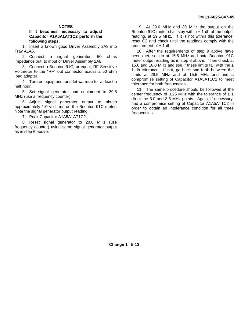
TM 11-6625-847-45
NOTESIf it becomes necessary to adjustCapacitor A1A5A1AT1C2 perform thefollowing steps.
1. Insert a known good Driver Assembly 2A8 intoTray A1A5.
2. Connect a signal generator, 50 ohmsimpedance out, to input of Driver Assembly 2A8.
3. Connect a Boonton 91C, or equal, RF SensitiveVoltmeter to the "RF" out connector across a 50 ohmload adapter.
4. Turn on equipment and let warmup for at least ahalf hour.
5. Set signal generator and equipment to 29.5MHz (use a frequency counter).
6. Adjust signal generator output to obtainapproximately 1.0 volt rms on the Boonton 91C meter.Note the signal generator output reading.
7. Peak Capacitor A1A5A1AT1C2.8. Reset signal generator to 20.0 MHz (use
frequency counter) using same signal generator outputas in step 6 above.
9. At 29.0 MHz and 30 MHz the output on theBoonton 91C meter shall stay within ± 1 db of the outputreading, at 29.5 MHz. If it is not within this tolerance,reset C2 and check until the readings comply with therequirement of ± 1 db
10. After the requirements of step 9 above havebeen met, set up at 15.5 MHz and note Boonton 91Cmeter output reading as in step 6 above. Then check at15.0 and 16.0 MHz and see if these limits fall with the ±1 db tolerance. If not, go back and forth between thelimits at 29.5 MHz and at 15.5 MHz and find acompromise setting of Capacitor A1A5AT1C2 to meettolerance for both frequencies.
11. The same procedure should be followed at thecenter frequency of 3.25 MHz with the tolerance of ± 1db at the 3.0 and 3.5 MHz points. Again, if necessary,find a compromise setting of Capacitor A1A5AT1C2 inorder to obtain an intolerance condition for all threefrequencies.
Change 1 5-13
TM 11-6625-847-45
CHAPTER 6
FOLDOUT ILLUSTRATIONS
This chapter contains fold-out schematic diagrams.
Change 1 6-1

TM 11-6625-847-45
Figure 6-1.
DELETED.
Change 1 6-2

TM 11-6625-847-45
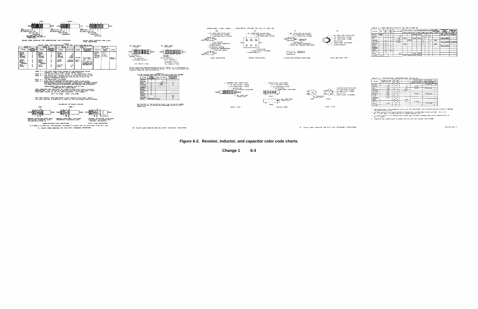
Figure 6-2. Resistor, inductor, and capacitor color code charts.
Change 1 6-3
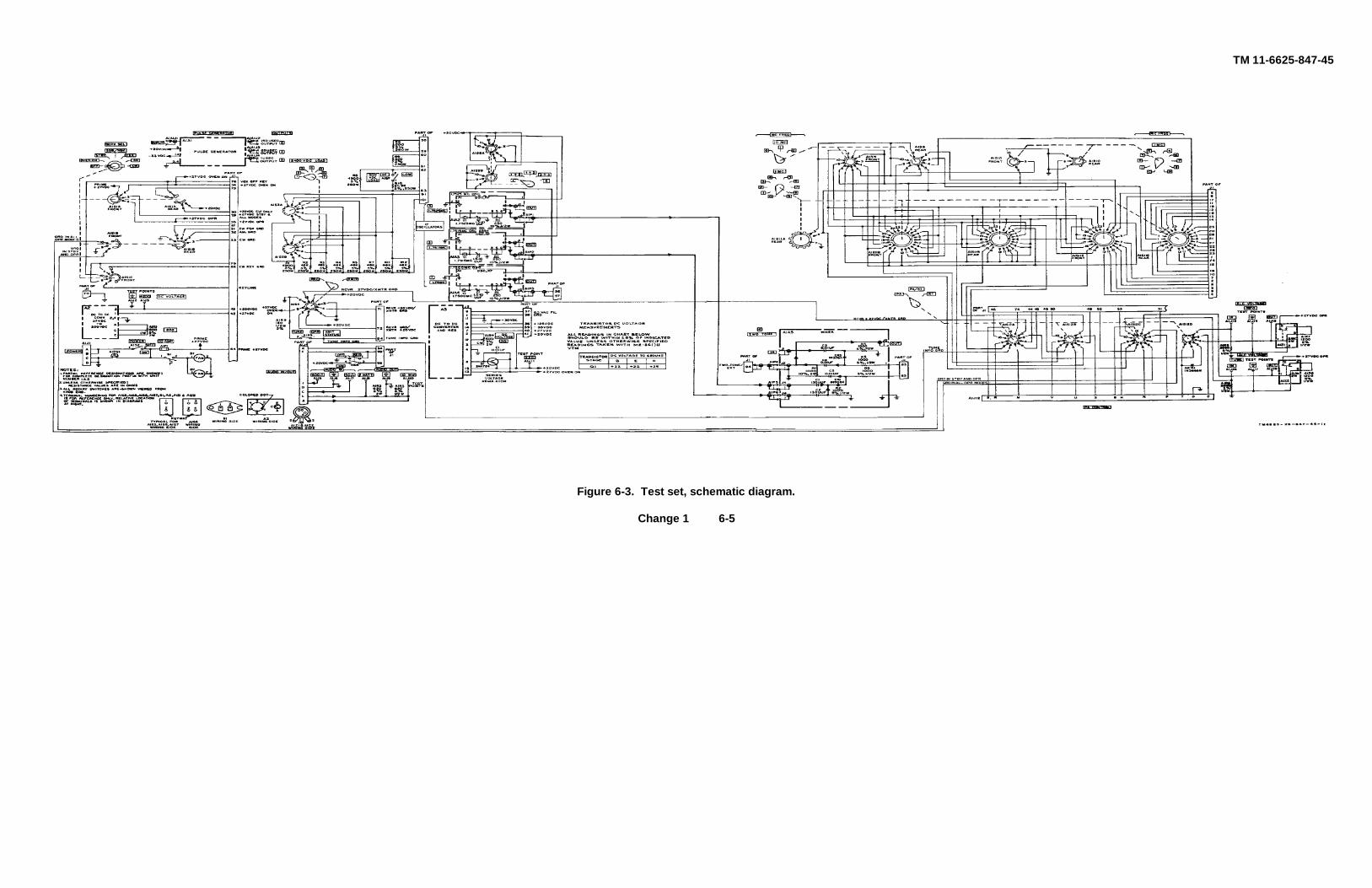
TM 11-6625-847-45
Figure 6-3. Test set, schematic diagram.
Change 1 6-5
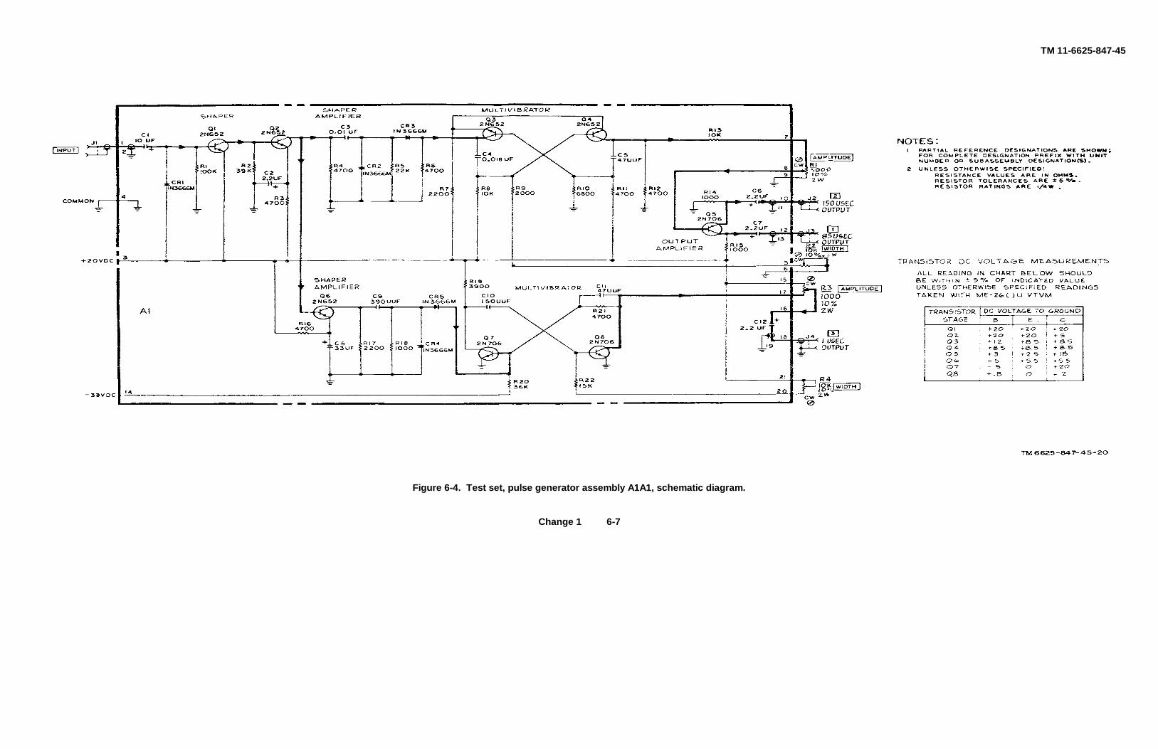
TM 11-6625-847-45
Figure 6-4. Test set, pulse generator assembly A1A1, schematic diagram.
Change 1 6-7
TM 11-6625-847-45
Figure 6-5. Test set, dc-to-dc converter and regulator assembly A3, schematic diagram.
Change 1 6-9
TM 11-6625-847-45
Figure 6-6. Test set IF oscillators A1A2, A1A3, and A1A4, schematic diagram.
6-11
TM 11-6625-847-45
Figure 6-7. Common module tray A1A1, schematic diagram.
Change 1 6-13
TM 11-6625-847-45
Figure 6-8. Common module tray A1A2, schematic diagram.
Change 1 6-15
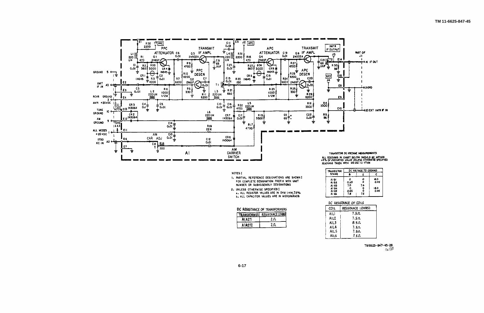
TM 11-6625-847-45
6-17
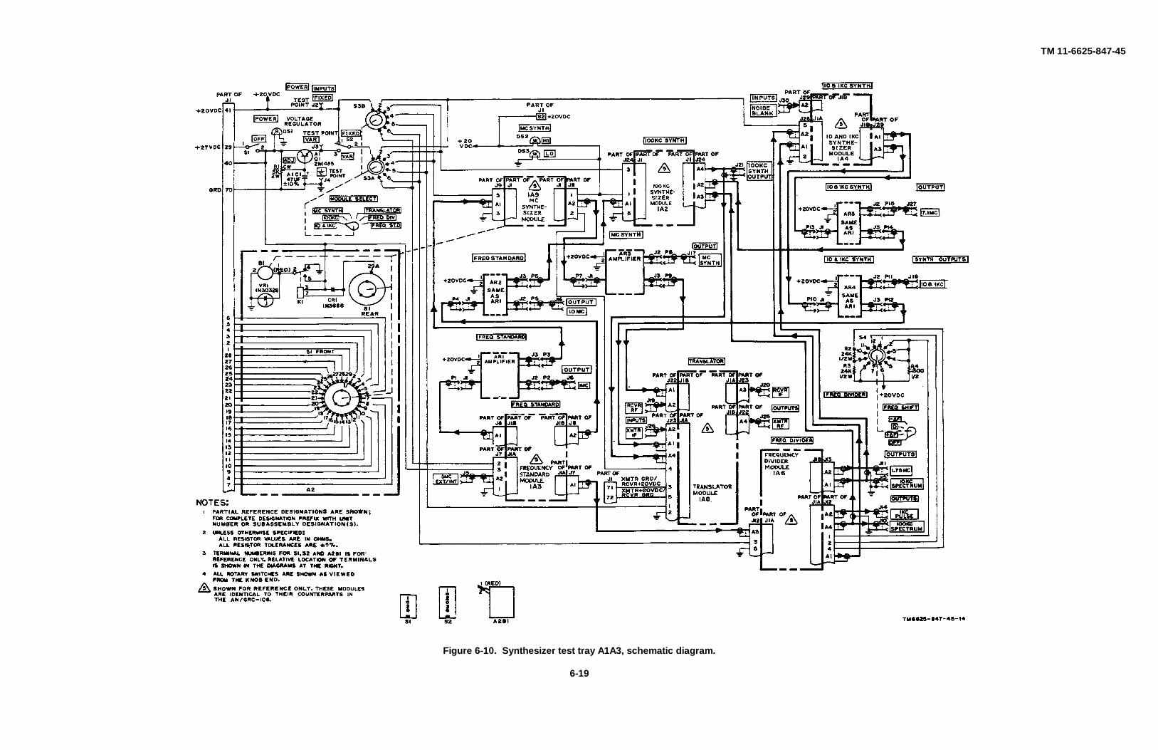
TM 11-6625-847-45
Figure 6-10. Synthesizer test tray A1A3, schematic diagram.
6-19
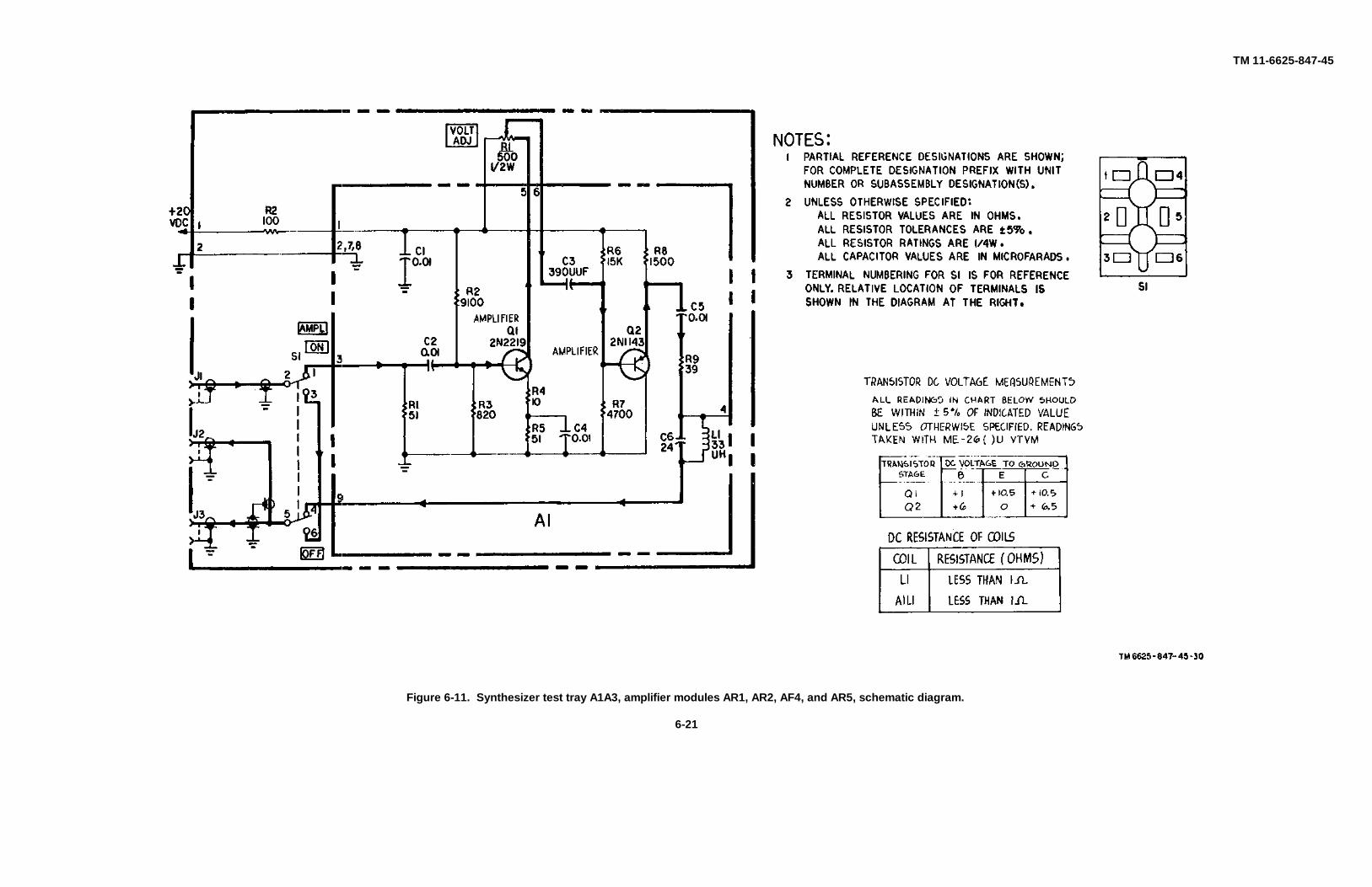
TM 11-6625-847-45
Figure 6-11. Synthesizer test tray A1A3, amplifier modules AR1, AR2, AF4, and AR5, schematic diagram.
6-21
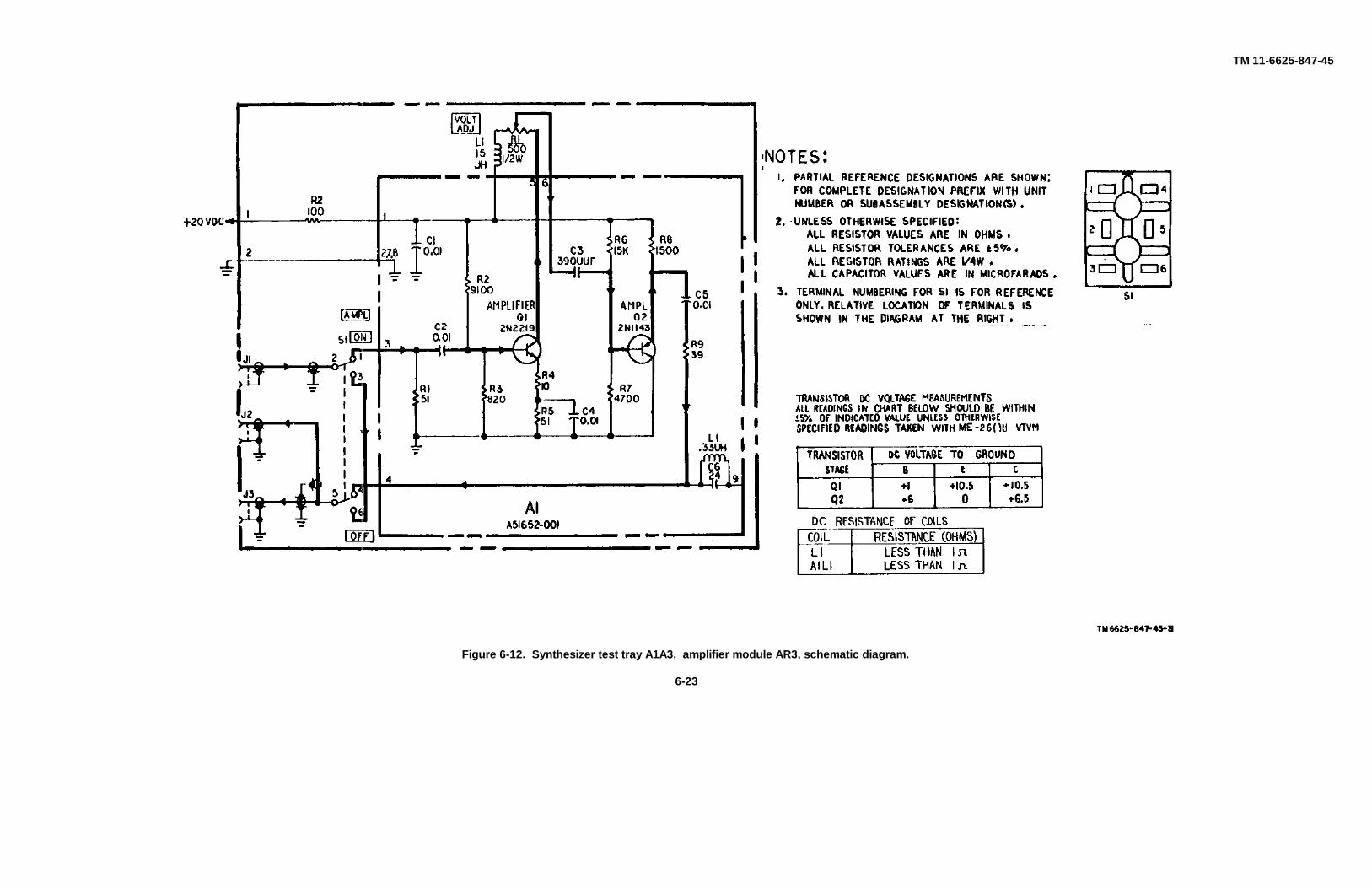
TM 11-6625-847-45
Figure 6-12. Synthesizer test tray A1A3, amplifier module AR3, schematic diagram.
6-23
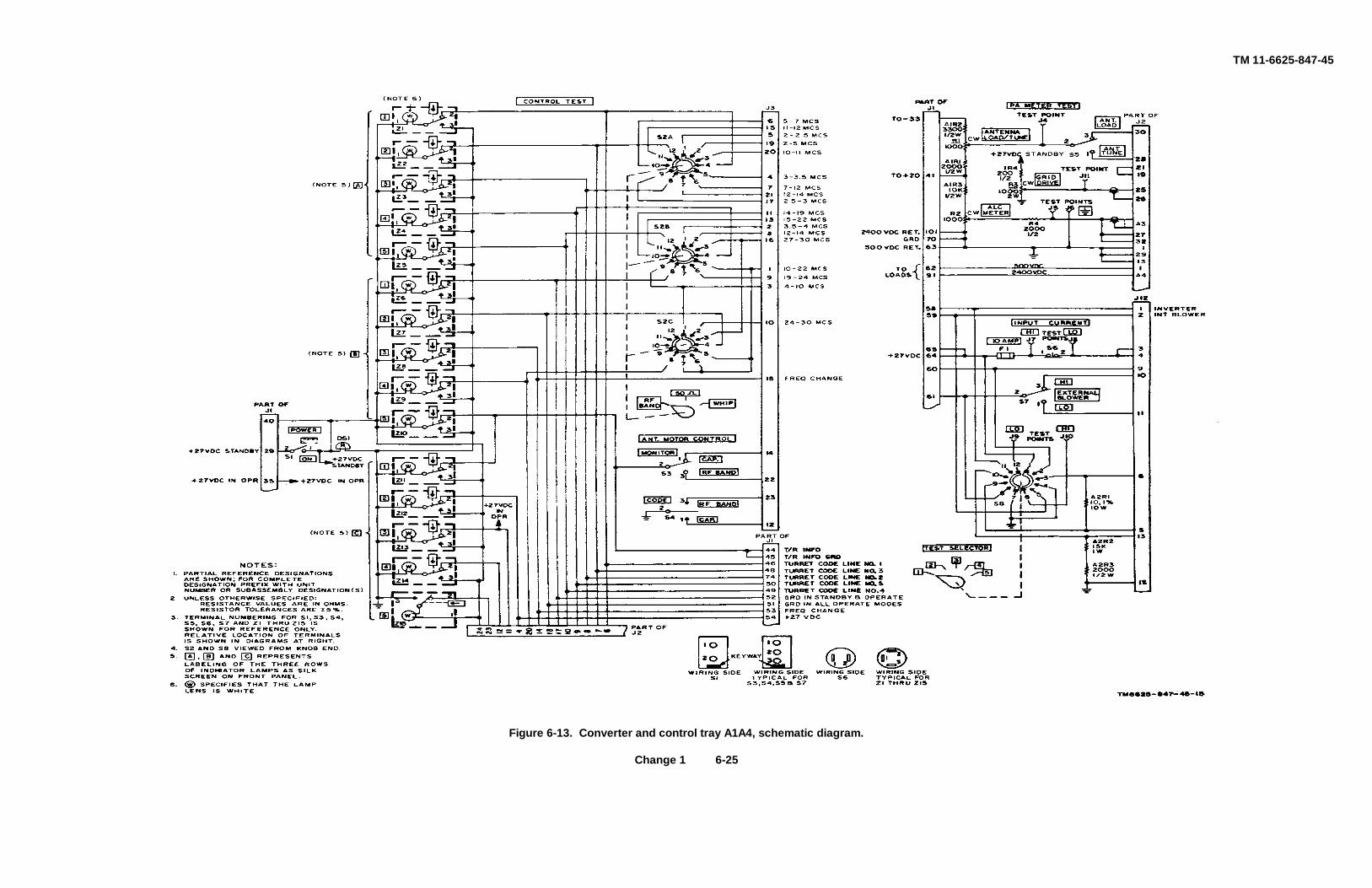
TM 11-6625-847-45
Figure 6-13. Converter and control tray A1A4, schematic diagram.
Change 1 6-25
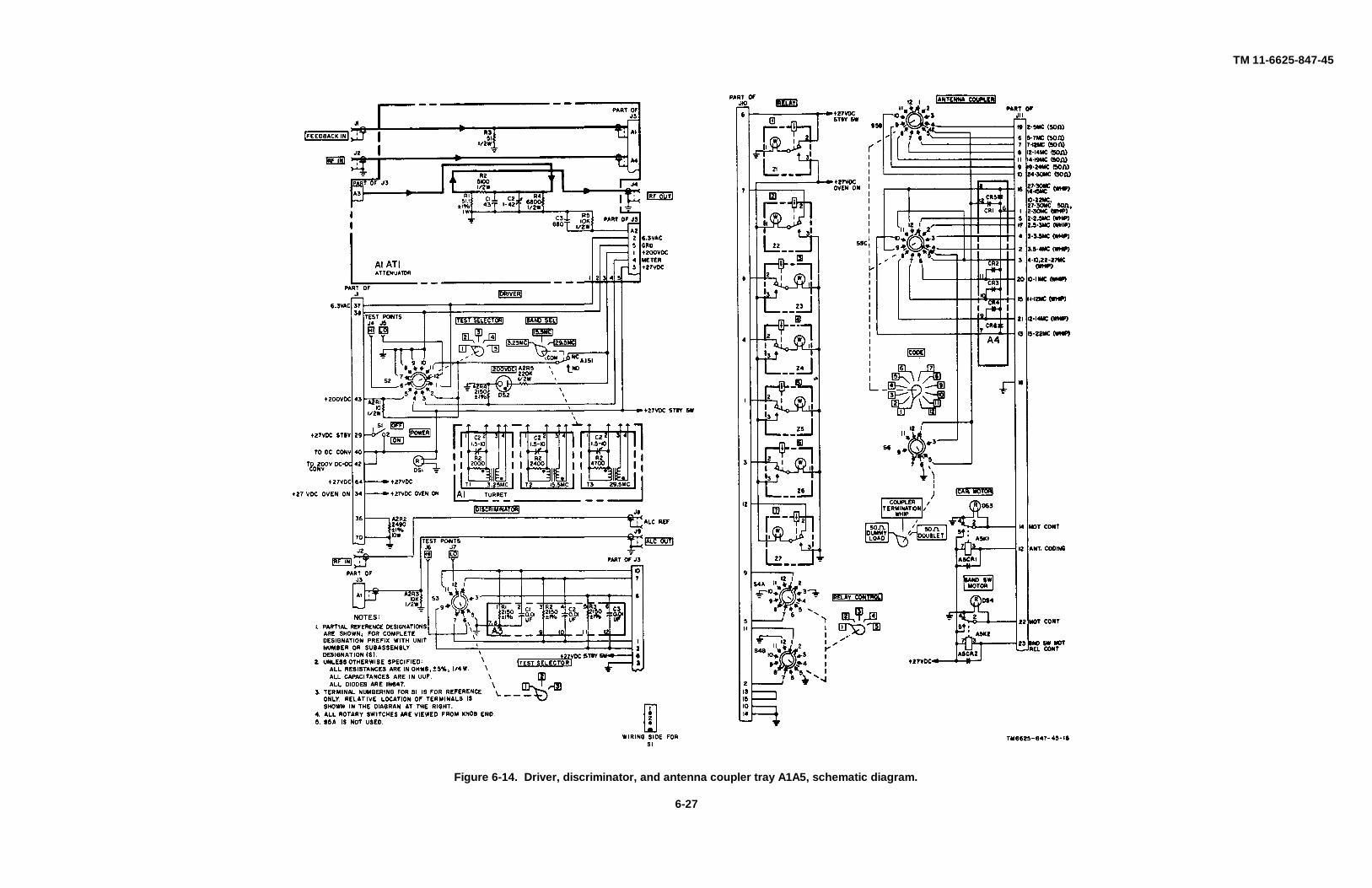
TM 11-6625-847-45
Figure 6-14. Driver, discriminator, and antenna coupler tray A1A5, schematic diagram.
6-27
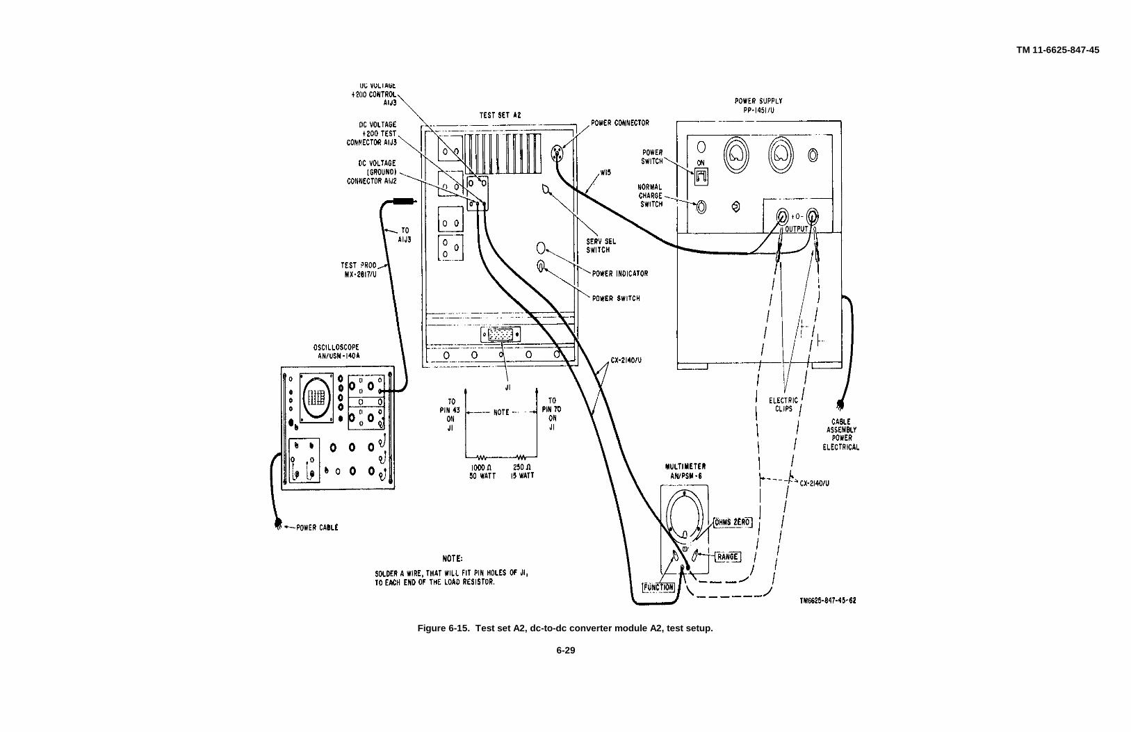
TM 11-6625-847-45
Figure 6-15. Test set A2, dc-to-dc converter module A2, test setup.
6-29
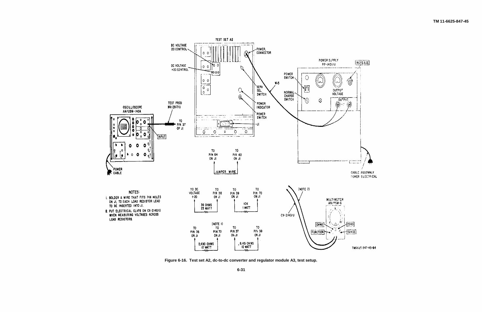
TM 11-6625-847-45
Figure 6-16. Test set A2, dc-to-dc converter and regulator module A3, test setup.
6-31
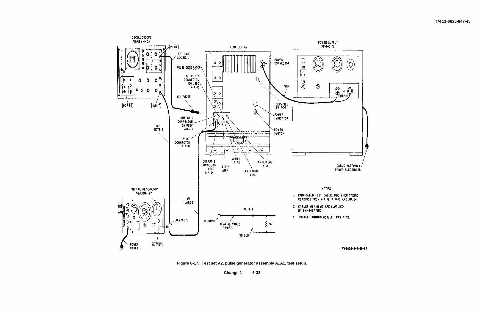
TM 11-6625-847-45
Figure 6-17. Test set A2, pulse generator assembly A1A1, test setup.
Change 1 6-33
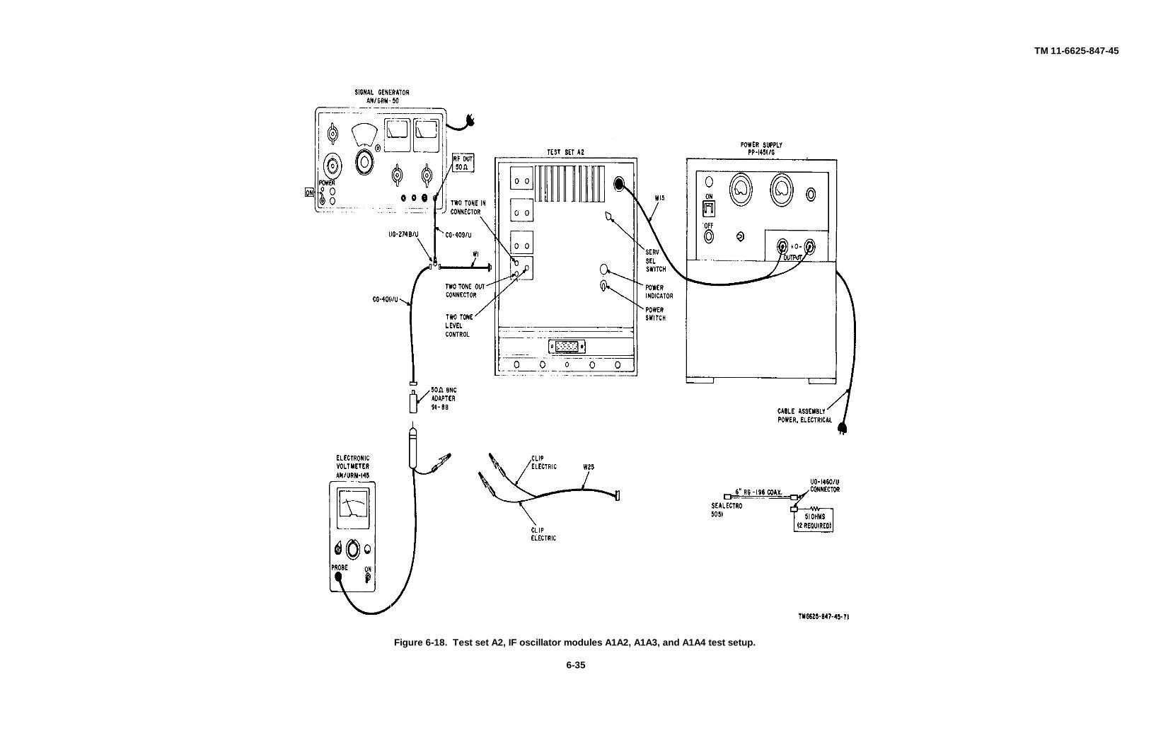
TM 11-6625-847-45
Figure 6-18. Test set A2, IF oscillator modules A1A2, A1A3, and A1A4 test setup.
6-35
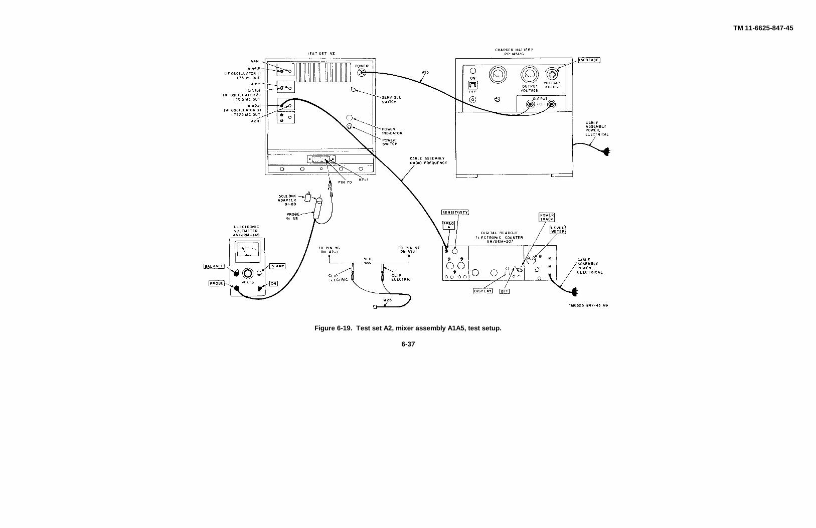
TM 11-6625-847-45
Figure 6-19. Test set A2, mixer assembly A1A5, test setup.
6-37
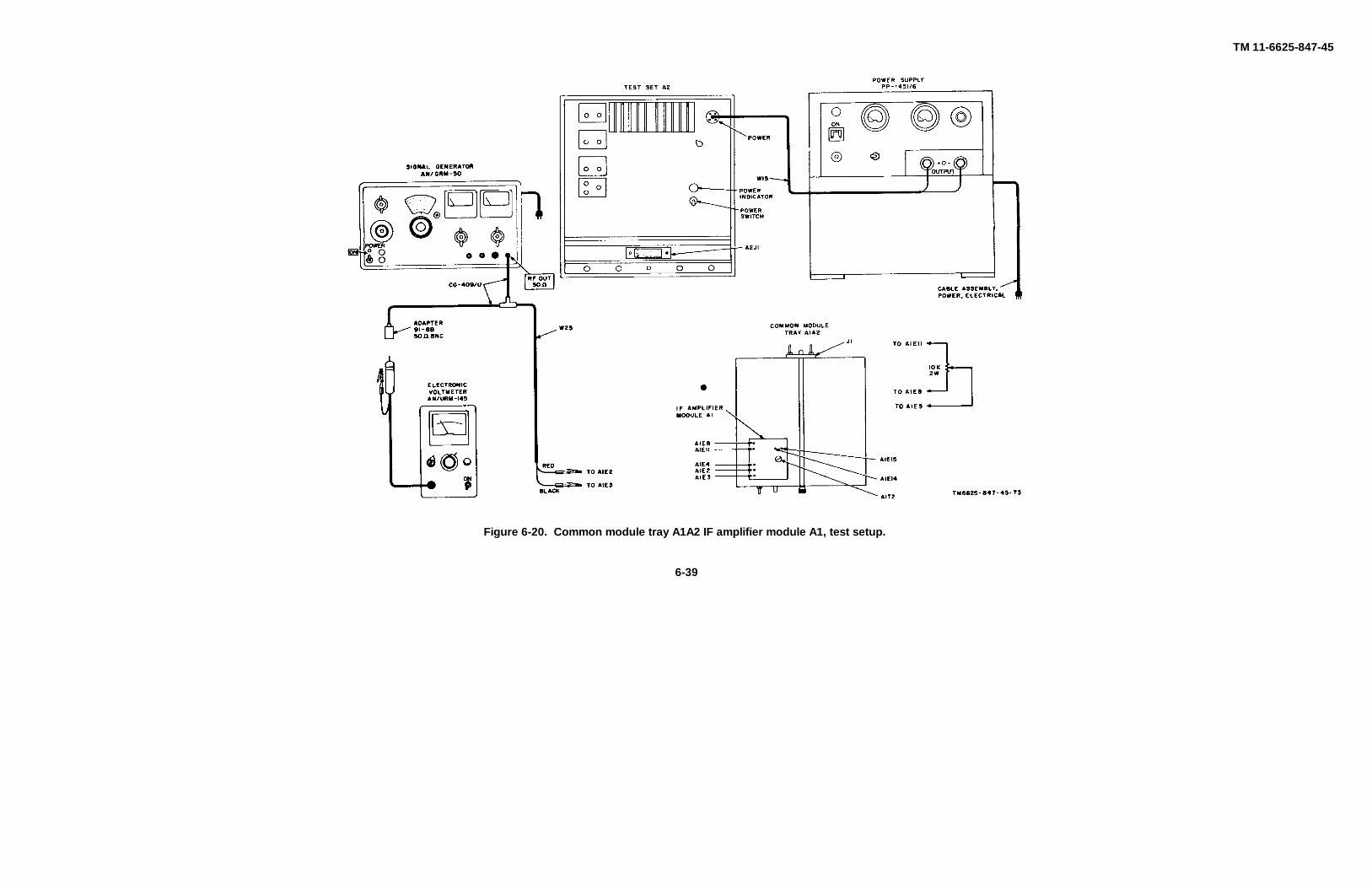
TM 11-6625-847-45
Figure 6-20. Common module tray A1A2 IF amplifier module A1, test setup.
6-39
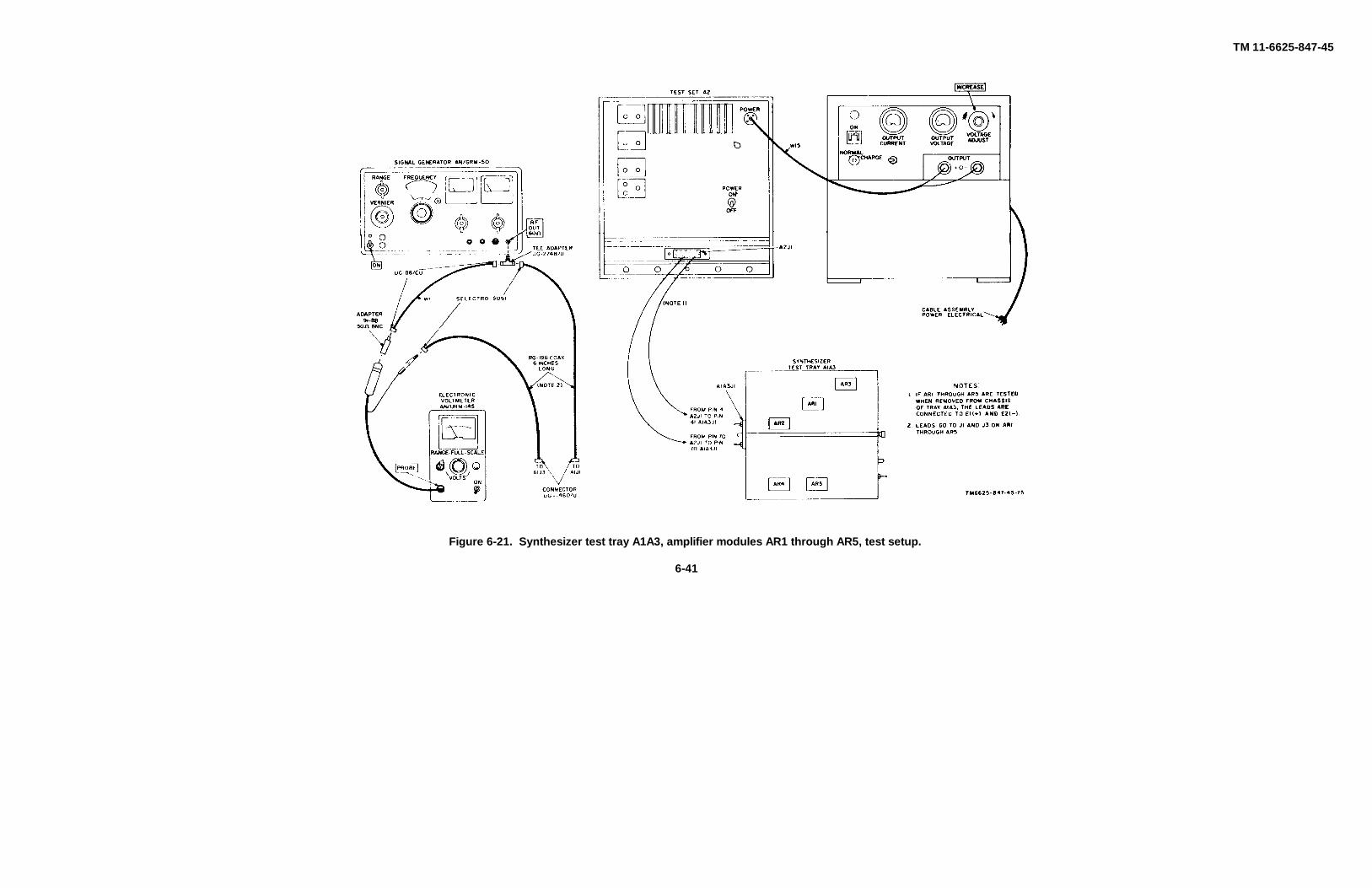
TM 11-6625-847-45
Figure 6-21. Synthesizer test tray A1A3, amplifier modules AR1 through AR5, test setup.
6-41
TM 11-6625-847-45
APPENDIX AREFERENCES
Following is a list of applicable publications that should be available to the GS and depot maintenance personnel for theSM442A/GRC:
AR 700-58 Report of Packaging and Handling Deficiencies.DA Pam 310-4 Index of Technical Manuals, Technical Bulletins, Supply Manuals Types 7,8,
and 9), Supply Bulletins, and Lubrication Orders.DA Pam 310-7 US Army Equipment Index of Modification Work Orders.SB 11-131 Vehicular Radio Sets and Authorized Installations.SB 38-100 Preservation, Packaging, and Packing Materials, Supplies, and Equipment
Used by the Army.TB SIG 291 Safety Measures to be Observed When Installing and Using Whip Antennas,
Field Type Masts, Towers, Antennas, and Metal Poles that are used withCommunication, Radar, and Direction Finder Equipment. (TO 31P5-1-1).
TB SIG 355-1 Depot Inspection Standard for Repaired Signal Equipment.TB SIG 35S2 Depot Inspection Standard for Refinishing Repaired Signal Equipment.TB SIG 355-3 Depot Inspection Standard for Moisture and Fungus Resistant Treatment.TB SIG 74610 Field Instructions for Painting and Preserving Electronics Command
Equipment.TM 11-5097 Spectrum Analyzers TS-723A/U, TS-723B/U, TS-723C/U, and TS723D/U (TO
33A1-664-1).TM 11-5820-520-12 Operator's and Organizational Maintenance Manual Including Repair Parts
and Special Tools Lists: Radio Sets AN/GRC(106 and AN/GRC-106A.TM 11-6130-236-12 Organizational Maintenance Manual: Charger, Battery PP-1451/G.TM 11-6130-247-15 Operator's, Organizational, DS, GS, and Depot Maintenance Manual
(Including Repair Parts and Special Tools List): Power Supply PP-3940/G.*TM 11-6625200-15 Operator's, Organizational, DS, GS, and Depot Maintenance Manual:* Multimeters ME-26A/U, ME-26B[U, ME-26C/U, and ME-26D/U.TM 11-6625475-10 Operator's Manual: Multimeters AN/PSM-6, AN/PSM-6A, and AN/PSM-6B.TM 11-6625-524-14 Operator, Organizational and Field Maintenance Manual: Voltmeter,
Electronic AN/URM-145.TM 11-6625-535-15 Operator, Organizational, DS, GS, and Depot Maintenance Manual: Osillos-
cope AN/USM-140A.TM 11-6625-535-15-1 Organizational, DS, GS, and Depot Maintenance Manual Including Repair
Parts and Special Tools List: Oscilloscopes AN/USM-140B, AN/USM-140C,AN/USM-141A, and AN/USM-141B.
TM 11-6625-683-15 Operator, Organizational, Direct Support, General Support, and DepotMaintenance Manual: Signal Generator ANtURM-127.
TM 114625-700-10 Operator's Manual: Digital Readout, Electronic Counter AN/USM-207.TM 11-26-847-12 Operator's, Organizational Maintenance Manual Including Repair Parts and
Special Tools List: Simulator, Radio Frequency SM442A/GRC.*TM 38750 The Army Maintenance Management System (TAMMS).TM 43-0139 Painting Instructions for Field Use.
Change 2 A-1
TM 11-6625-847-45
INDEX
Paragraph Page
AdjustmentsIF amplifier subassembly A2, tray A1A2- ...................................................................... 3-56 3--27Synthesizer test tray A1A3 ............................................................................................ 3-56 8-2
Applicability, depot overhaul standards .................................................................................. 5-2 6-1
Block diagrams ...................................................................................................................... 1-4 1-3Module testing .............................................................................................................. 1-6 1-4System testing .............................................................................................................. 1-6 1-9
Characteristics, test equipment .............................................................................................. 3-4 8-1Circuit transistor:
Resistance measurements ............................................................................................ 2-17b 2-4Voltage ......................................................................................................................... 2-17a 2-6
Cleaning ......................................................................................................................... 3-7 3-2Common:
Module:Tray A1A1 .............................................................................................................. 1-15 1-13
Operational performance test ........................................................................... 5-9 5-4Tray A1A2 ............................................................................................................... 1-16 1-14
Operational performance test ........................................................................... 5-11 5-5Names ................................................................................................................... 1-3 1-1
Converter and control tray A1A4 ............................................................................................ 1-23 1-21Operational performance test ........................................................................................ 5-15 5-11
Depot:General ................................................................................................................... 5-1 5-1Overhaul standards ...................................................................................................... 5-2 5-1Testing ................................................................................................................... 5-5 5-1
Disassembly:Amplifier modules AR1, AR2, AR3, AR4, and AR5, tray A1A3 ...................................... 3-50 3-22Component boards, tray A1A1 ...................................................................................... 3-38 3-19Dc-to-dc converter and regulator module A3 ................................................................. 3-26 3-16Gear drive assembly ..................................................................................................... 3-11 3-3Idler assembly tray A1A1 .............................................................................................. 3-35 3-18IF amplifier subassembly A2, tray A1A2 ....................................................................... 3-44 3-19Mixer module ................................................................................................................ 3-20 3-11Oscillator submodules A2A1A2, A2A1A3, and A2A1A4 ................................................. 3-22 3-12Pulse generator assembly ............................................................................................. 3-17 3-7Sprocket assembly, tray A1A1:
Group A .................................................................................................................. 3-29 3-16Group B .................................................................................................................. 3-32 3-17
Terminal board:Tray A1A2 .............................................................................................................. 3-41 3-19Tray A1A4 .............................................................................................................. 3-53 3-23
Turret transformer assembly ......................................................................................... 3-14 3-6Driver, discriminator, and antenna coupler tray A1A5 ............................................................. 1-24 1-22
Operational performance test ........................................................................................ 5-17 5-12
Electronic circuits:Common module tray A1A2 .......................................................................................... 1-20 1-17Synthesizer test tray A1A3 ............................................................................................ 1-22 1-21
1-1
TM 11-6625-847-45Paragraph Page
Functional analysis, test set ;Dc-to-dc converter and regulator module A2A3 ............................................................. 1-10 1-9IF oscillator circuit.......................................................................................................... 1-11 1-11Mc fruency selection circuit ........................................................................................... 1-14 1-13Mixer assembly A1A5 ................................................................................................... 1-12 1-17Pulse generator subassembly A2AA1 ........................................................................... 1-9 1-SERV SEL switch ......................................................................................................... 1-13 1-11
General :Support:
Other equipment ..................................................................................................... 4-2c 4-2Test:Cable fabrication .................................................................................................... 4-4 4-2Equipments, tools, and materials ............................................................................ 4-2 4-1Power supply .......................................................................................................... 4-3 4-2Setups ................................................................................................................... 4-4 4-2Summary, data ....................................................................................................... 4-12 4-18Testing, general ...................................................................................................... 4-1 4-1
Troubleshooting instructions .......................................................................................... 2-1 21Index , publications ................................................................................................................ 1-2 1-1Inspection ................................................................................................................... 3-8 3-2Isolating trouble within stage .................................................................................................. 2-17 2-6Isolation ................................................................................................................... 2-2d 2-2Location ................................................................................................................... 2-2c 2-1Lubrication ................................................................................................................... 3-9 3-3Mechanical assemblies :
Common module tray A1A1 .......................................................................................... 1-26 1-25Driver, discriminator, and antenna coupler tray A1A5 ................................................... 1-28 1-25Functional operation ..................................................................................................... 1-25 1-25Synthesizer test try A1A3 .............................................................................................. 1-27 1-25
Organization, troubleshooting procedures .............................................................................. 2-2 2-1Parts replacement techniques, general ................................................................................... 3-1 8-1Power supply, general support testing .................................................................................... 4-3 4-2Power supply requirements .................................................................................................... 2-5 2-3Reassembly:
Amplifier modules AR1, AR2, AR8, AM, and AR5, tray A1A3 ....................................... 3-51 3-22Assemblies:
Gear drive .............................................................................................................. 3-12 3-3Idler, tray A1A1 ...................................................................................................... 3-36 3-18IF subassembly A2, tray A1A2 ................................................................................ 3-45 3-19Mixer ................................................................................................................... 3-21 3-11Pulse generator ...................................................................................................... 3-18 3-10Sprocket, tray A1A1:
Group A ........................................................................................................... 3-30 3-17Group B ........................................................................................................... 3-33 3-17
Component boards, tray A1A1 ...................................................................................... 3-39 3-19Dc-to-dc converter and regulator module A3.................................................................. 3--27 3-16Oscillator subassemblies A2A1A2, A2A1AS, and A21A4 .............................................. 3-24 3-15Terminal boards:
Tray A1A2 .............................................................................................................. 3-42 3-19Tray A1A4 .............................................................................................................. 3-54 3-23
Removal:Amplifier modules AR1, AR2, AR3, AR4, and AR6, tray A1A3 ...................................... 3-49 3-23Assemblies:
Gear drive .............................................................................................................. 3-10 3-3Idler, tray A1A1 ...................................................................................................... 3-34 3-18Mixer - ................................................................................................................. 3-19 3-10Oscillator A2A1A2, A2A1A3, and A2A1A4 .............................................................. 3-22 3-12
1-2
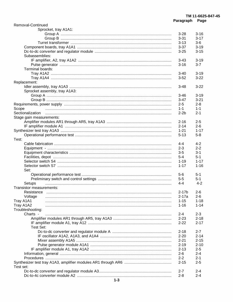
TM 11-6625-847-45Paragraph Page
Removal-ContinuedSprocket, tray A1A1:
Group A ..................................................................................................... 3-28 3-16Group B ..................................................................................................... 3-31 3-17
Turret transformer ............................................................................................ 3-13 3-6Component boards, tray A1A1 ...................................................................................... 3-37 3-19Dc-to-dc converter and regulator module ...................................................................... 3-25 3-15Subassemblies:
IF amplifier, A2, tray A1A2 ..................................................................................... 3-43 3-19Pulse generator ...................................................................................................... 3-16 3-7
Terminal boards:Tray A1A2 .............................................................................................................. 3-40 3-19Tray A1A4 .............................................................................................................. 3-52 3-22
Replacement:Idler assembly, tray A1A3 ............................................................................................. 3-48 3-22Sprocket assembly, tray A1A3:
Group A .................................................................................................................. 3-46 3-19Group B .................................................................................................................. 3-47 3-21
Requirements, power supply .................................................................................................. 2-5 2-8Scope ................................................................................................................... 1-1 1-1Sectionalization ................................................................................................................... 2-2b 2-1Stage gain measurements:
Amplifier modules AR1 through AR5, tray A1A3 ........................................................... 2-16 2-5IF amplifier module A1 ................................................................................................. 2-14 2-6
Synthesizer test tray A1A3 ..................................................................................................... 1-21 1-17Operational performance test ........................................................................................ 5-13 5-8
Test:Cable fabrication ........................................................................................................... 4-4 4-2Equipment - ................................................................................................................. 2-3 2-2Equipment characteristics ............................................................................................. 3-5 3-1Facilities, depot ............................................................................................................ 5-4 5-1Selector switch S4 ........................................................................................................ 1-19 1-17Selector switch S7 ........................................................................................................ 1-17 1-16Set:
Operational performance test .................................................................................. 5-6 5-1Preliminary switch and control settings ................................................................... 5-5 5-1
Setups ................................................................................................................... 4-4 4-2Transistor measurements:
Resistance .................................................................................................................. 2-17b 2-6Voltage ................................................................................................................... 2-17a 2-6
Tray A1A1 ................................................................................................................... 1-15 1-18Tray A1A2 ................................................................................................................... 1-16 1-14Troubleshooting:
Charts - ................................................................................................................... 2-4 2-3Amplifier modules AR1 through AR5, tray A1A3 ..................................................... 2-23 2-18IF amplifier module A1, tray A12 ............................................................................ 2-22 2-17Test Set:
Dc-to-dc converter and regulator module A ...................................................... 2-18 2-7IF oscillator A1A2, A1A3, and A1A4 ................................................................. 2-20 2-14Mixer assembly A1A5 ....................................................................................... 2-21 2-15Pulse generator module A1A1 .......................................................................... 2-19 2-10
IF amplifier module A1, tray A1A2 .......................................................................... 2-13 2-5Information, general ...................................................................................................... 2-6 2-4Procedures ................................................................................................................... 2-2 2-1
Synthesizer test tray A1A3, amplifier modules AR1 through AR6 ........................................... 2-15 2-5Test set:
Dc-to-dc converter and regulator module A3.................................................................. 2-7 2-4Dc-to-4c converter module A2 ...................................................................................... 2-8 2-4
1-3
TM 11-6625-847-45
Paragraph Page
Troubleshooting-ContinuedTest set-Continued
IF oscillator modules A1A2, A1A3, A1A4................................................................. 2-11 2-4Mixer module A1A5................................................................................................. 2-12 2-3Pulse Rotor module A1A1 ....................................................................................... 2-9 2-12
Voice modes switch S8 ............................................................................................................ 1-3 1-6
Waveform check, test set, generator module A1A1 ................................................................ 2-10 2-4
1-4
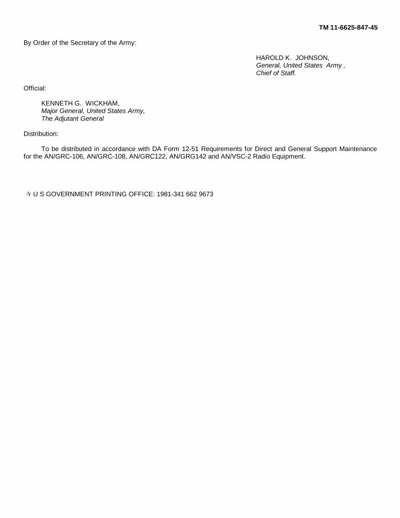
TM 11-6625-847-45
By Order of the Secretary of the Army:
HAROLD K. JOHNSON,General, United States Army ,Chief of Staff.
Official:
KENNETH G. WICKHAM,Major General, United States Army,The Adjutant General
Distribution:
To be distributed in accordance with DA Form 12-51 Requirements for Direct and General Support Maintenancefor the AN/GRC-106, AN/GRC-108, AN/GRC122, AN/GRG142 and AN/VSC-2 Radio Equipment.
U S GOVERNMENT PRINTING OFFICE: 1981-341 662 9673
The Metric System and Equivalents
Liquid MeasureLinear Measure
1 centiliter = 10 milliliters = .34 fl. ounce1 centimeter = 10 millimeters = .39 inch 1 deciliter = 10 centiliters = 3.38 fl. ounces1 decimeter = 10 centimeters = 3.94 inches 1 liter = 10 deciliters = 33.81 fl. ounces1 meter = 10 decimeters = 39.37 inches 1 dekaliter = 10 liters = 2.64 gallons1 dekameter = 10 meters = 32.8 feet 1 hectoliter = 10 dekaliters = 26.42 gallons1 hectometer = 10 dekameters = 328.08 feet 1 kiloliter = 10 hectoliters = 264.18 gallons1 kilometer = 10 hectometers = 3,280.8 feet
Square MeasureWeights
1 sq. centimeter = 100 sq. millimeters = .155 sq. inch1 centigram = 10 milligrams = .15 grain 1 sq. decimeter = 100 sq. centimeters = 15.5 sq. inches1 decigram = 10 centigrams = 1.54 grains 1 sq. meter (centare) = 100 sq. decimeters = 10.76 sq. feet1 gram = 10 decigram = .035 ounce 1 sq. dekameter (are) = 100 sq. meters = 1,076.4 sq. feet1 dekagram = 10 grams = .35 ounce 1 sq. hectometer (hectare) = 100 sq. dekameters = 2.47 acres1 hectogram = 10 dekagrams = 3.52 ounces 1 sq. kilometer = 100 sq. hectometers = .386 sq. mile1 kilogram = 10 hectograms = 2.2 pounds1 quintal = 100 kilograms = 220.46 pounds Cubic Measure1 metric ton = 10 quintals = 1.1 short tons
1 cu. centimeter = 1000 cu. millimeters = .06 cu. inch1 cu. decimeter = 1000 cu. centimeters = 61.02 cu. inches1 cu. meter = 1000 cu. decimeters = 35.31 cu. feet
Approximate Conversion Factors
To change To Multiply by To change To Multiply by
inches centimeters 2.540 ounce-inches newton-meters .007062feet meters .305 centimeters inches .394yards meters .914 meters feet 3.280miles kilometers 1.609 meters yards 1.094square inches square centimeters 6.451 kilometers miles .621square feet square meters .093 square centimeters square inches .155square yards square meters .836 square meters square feet 10.764square miles square kilometers 2.590 square meters square yards 1.196acres square hectometers .405 square kilometers square miles .386cubic feet cubic meters .028 square hectometers acres 2.471cubic yards cubic meters .765 cubic meters cubic feet 35.315fluid ounces milliliters 29.573 cubic meters cubic yards 1.308pints liters .473 milliliters fluid ounces .034quarts liters .946 liters pints 2.113gallons liters 3.785 liters quarts 1.057ounces grams 28.349 liters gallons .264pounds kilograms .454 grams ounces .035short tons metric tons .907 kilograms pounds 2.205pound-feet newton-meters 1.365 metric tons short tons 1.102pound-inches newton-meters .11375
Temperature (Exact)
o F Fahrenheit 5/9 (after Celsius o Ctemperature subtracting 32) temperature

PIN #: 013599

This fine document...
Was brought to you by me:
Liberated Manuals -- free army and government manuals
Why do I do it? I am tired of sleazy CD-ROM sellers, who take publicly available information, slap “watermarks” and other junk on it, and sell it. Those masters of search engine manipulation make sure that their sites that sell free information, come up first in search engines. They did not create it... They did not even scan it... Why should they get your money? Why are not letting you give those free manuals to your friends?
I am setting this document FREE. This document was made by the US Government and is NOT protected by Copyright. Feel free to share, republish, sell and so on.
I am not asking you for donations, fees or handouts. If you can, please provide a link to liberatedmanuals.com, so that free manuals come up first in search engines:
<A HREF=http://www.liberatedmanuals.com/>Free Military and Government Manuals</A>
– SincerelyIgor Chudovhttp://igor.chudov.com/
– Chicago Machinery Movers