Embed Size (px)
Citation preview

www.ti.com
FEATURES APPLICATIONS
D PACKAGE(TOP VIEW)
1
2
3
4
8
7
6
5
NCVCC+
OUTNC
NCIN–IN+VCC–
NC – No internal connection
DBV PACKAGE(TOP VIEW)
1
2
3
5
4
OUTVCC+
IN+
VCC–
IN–
DCK PACKAGE(TOP VIEW)
1
2
3
6
4
OUTVCC+
IN+
NC
IN–5 VCC–
DESCRIPTION/ORDERING INFORMATION
TLV7211,, TLV7211ACMOS COMPARATORS
WITH RAIL-TO-RAIL INPUT AND PUSH-PULL OUTPUTSLCS149B–AUGUST 2006–REVISED JANUARY 2007
• Battery-Powered Products• Parameters Specified at 2.7-V, 5-V, and 15-VSupplies • Notebooks and PDAs
• Mobile Communications• Supply Current 7 µA (Typ) at 5 V• Alarm and Security Circuits• Response Time 4 µs (Typ) at 5 V• Direct Sensor Interface• Push-Pull Output• Replaces Amplifiers Used as Comparators• Input Common-Mode Range Beyond
With Better Performance and Lower CurrentVCC– and VCC+
• Low Input Current
The TLV7211 and TLV7211A are micropower CMOS comparators available in the space-saving SOT-23-5package. This makes the comparators ideal for space- and weight-critical designs. The TLV7211A features aninput offset voltage of 5 mV, and the TLV7211 features an input offset voltage of 15 mV.
The main benefits of the SOT-23-5 package are most apparent in small portable electronic devices, such asmobile phones, pagers, notebook computers, personal digital assistants, and PCMCIA cards. The rail-to-railinput voltage makes the TLV7211 or TLV7211A a good choice for sensor interfacing, such as light detectorcircuits, optical and magnetic sensors, and alarm and status circuits.
The SOT-23-5 package's small size allows it to fit into tight spaces on PC boards.
ORDERING INFORMATION
VOSTA PACKAGE (1) ORDERABLE PART NUMBER TOP-SIDE MARKING (2)(MAX)
Reel of 2500 TLV7211AIDRSOIC – D 7211AI
Tube of 75 TLV7211AID
5 mV SOT-23-5 – DBV Reel of 3000 TLV7211AIDBVR YBN_
Reel of 3000 TLV7211AIDCKRSOT (SC-70) – DCK Y8_
Reel of 250 TLV7211AIDCKT–40°C to 85°C
Reel of 2500 TLV7211IDRSOIC – D TY7211
Tube of 75 TLV7211ID
15 mV SOT-23-5 – DBV Reel of 3000 TLV7211IDBVR YBK_
Reel of 3000 TLV7211IDCKRSOT (SC-70) – DCK Y7_
Reel of 250 TLV7211IDCKT
(1) Package drawings, standard packing quantities, thermal data, symbolization, and PCB design guidelines are available atwww.ti.com/sc/package.
(2) DBV/DCK: The actual top-side marking has one additional character that designates the assembly/test site.
Please be aware that an important notice concerning availability, standard warranty, and use in critical applications of TexasInstruments semiconductor products and disclaimers thereto appears at the end of this data sheet.
PRODUCTION DATA information is current as of publication date. Copyright © 2006–2007, Texas Instruments IncorporatedProducts conform to specifications per the terms of the TexasInstruments standard warranty. Production processing does notnecessarily include testing of all parameters.
www.ti.com
IN–
IN+
OUT
Absolute Maximum Ratings (1)
ESD Protection
Recommended Operating Conditions
TLV7211,, TLV7211ACMOS COMPARATORSWITH RAIL-TO-RAIL INPUT AND PUSH-PULL OUTPUTSLCS149B–AUGUST 2006–REVISED JANUARY 2007
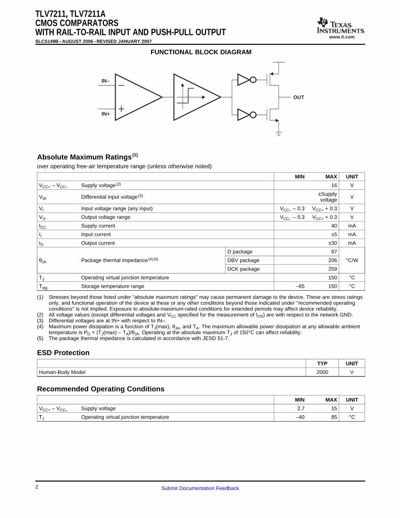
FUNCTIONAL BLOCK DIAGRAM
over operating free-air temperature range (unless otherwise noted)
MIN MAX UNIT
VCC+ – VCC– Supply voltage (2) 16 V
±SupplyVID Differential input voltage (3) Vvoltage
VI Input voltage range (any input) VCC– – 0.3 VCC+ + 0.3 V
VO Output voltage range VCC– – 0.3 VCC+ + 0.3 V
ICC Supply current 40 mA
II Input current ±5 mA
IO Output current ±30 mA
D package 97
θJA Package thermal impedance (4) (5) DBV package 206 °C/W
DCK package 259
TJ Operating virtual junction temperature 150 °C
Tstg Storage temperature range –65 150 °C
(1) Stresses beyond those listed under "absolute maximum ratings" may cause permanent damage to the device. These are stress ratingsonly, and functional operation of the device at these or any other conditions beyond those indicated under "recommended operatingconditions" is not implied. Exposure to absolute-maximum-rated conditions for extended periods may affect device reliability.
(2) All voltage values (except differential voltages and VCC specified for the measurement of IOS) are with respect to the network GND.(3) Differential voltages are at IN+ with respect to IN–.(4) Maximum power dissipation is a function of TJ(max), θJA, and TA. The maximum allowable power dissipation at any allowable ambient
temperature is PD = (TJ(max) – TA)/θJA. Operating at the absolute maximum TJ of 150°C can affect reliability.(5) The package thermal impedance is calculated in accordance with JESD 51-7.
TYP UNIT
Human-Body Model 2000 V
MIN MAX UNIT
VCC+ – VCC– Supply voltage 2.7 15 V
TJ Operating virtual junction temperature –40 85 °C
2 Submit Documentation Feedback
www.ti.com
2.7-V Electrical Characteristics
TLV7211,, TLV7211ACMOS COMPARATORS
WITH RAIL-TO-RAIL INPUT AND PUSH-PULL OUTPUTSLCS149B–AUGUST 2006–REVISED JANUARY 2007
VCC+ = 2.7 V, VCC– = GND, VCM = VO = VCC+/2, and RL > 1 MΩ (unless otherwise noted)
TLV7211A TLV7211PARAMETER TEST CONDITIONS TJ UNIT
MIN TYP MAX MIN TYP MAX
25°C 3 5 3 15VOS Input offset voltage mV
–40°C to 85°C 8 18
Input offset voltageTCVOS 25°C 1 1 µV/°Ctemperature drift
Input offset voltage 25°C 3.3 3.3 µV/monthaverage drift (1)
IB Input current 25°C 0.04 0.04 pA
IOS Input offset current 25°C 0.02 0.02 pA
Common-modeCMRR 0 ≤ VCM ≤ 2.7 V 25°C 75 75 dBrejection ratio
Power-supply rejectionPSRR 2.7 V ≤ VCC+ ≤ 15 V 25°C 80 80 dBratio
AV Voltage gain 25°C 100 100 dB
25°C 2.9 3 2.9 3CMRR > 55 dB
–40°C to 85°C 2.7 2.7Input common-modeCMVR Vvoltage range 25°C –0.3 –0.2 –0.3 –0.2CMRR > 55 dB
–40°C to 85°C 0 0
25°C 2.4 2.5 2.4 2.5High-level outputVOH Iload = 2.5 mA Vvoltage –40°C to 85°C 2.3 2.3
25°C 0.2 0.3 0.2 0.3Low-level outputVOL Iload = 2.5 mA Vvoltage –40°C to 85°C 0.4 0.4
25°C 7 12 7 12VOUT = Low
–40°C to 85°C 14 14ICC Supply current µA
25°C 5 10 5 10VOUT = High-Idle
–40°C to 85°C 12 12
(1) Input offset voltage average drift is calculated by dividing the accelerated operating life VOS drift by the equivalent operational time. Thisrepresents worst-case input conditions and includes the first 30 days of drift.
3Submit Documentation Feedback

www.ti.com
5-V Electrical Characteristics
TLV7211,, TLV7211ACMOS COMPARATORSWITH RAIL-TO-RAIL INPUT AND PUSH-PULL OUTPUTSLCS149B–AUGUST 2006–REVISED JANUARY 2007
VCC+ = 5 V, VCC– = GND, VCM = VO = VCC+/2, and RL > 1 MΩ (unless otherwise noted)
TLV7211A TLV7211PARAMETER TEST CONDITIONS TJ UNIT
MIN TYP MAX MIN TYP MAX
25°C 3 5 3 15VOS Input offset voltage mV
–40°C to 85°C 8 18
Input offset voltageTCVOS 25°C 1 1 µV/°Ctemperature drift
Input offset voltage 25°C 3.3 3.3 µV/monthaverage drift (1)
IB Input current 25°C 0.04 0.04 pA
IOS Input offset current 25°C 0.02 0.02 pA
Common-modeCMRR 25°C 75 75 dBrejection ratio
Power-supply rejectionPSRR 5 V ≤ VCC+ ≤ 10 V 25°C 80 80 dBratio
AV Voltage gain 25°C 100 100 dB
25°C 5.2 5.3 5.2 5.3CMRR > 55 dB
–40°C to 85°C 5 5Input common-modeCMVR Vvoltage range 25°C –0.3 –0.2 –0.3 –0.2CMRR > 55 dB
–40°C to 85°C 0 0
25°C 4.6 4.8 4.6 4.8High-level outputVOH Iload = 5 mA Vvoltage –40°C to 85°C 4.45 4.45
25°C 0.2 0.4 0.2 0.4Low-level outputVOL Iload = 5 mA Vvoltage –40°C to 85°C 0.55 0.55
25°C 7 14 7 14VOUT = Low
–40°C to 85°C 18 18ICC Supply current µA
25°C 5 10 5 10VOUT = High-Idle
–40°C to 85°C 13 13
Short-circuit outputIOH Isource 25°C 30 30 mAcurrent
Short-circuit outputIOL Isink, VO < 12 V (2) 25°C 45 45 mAcurrent
(1) Input offset voltage average drift is calculated by dividing the accelerated operating life VOS drift by the equivalent operational time. Thisrepresents worst-case input conditions and includes the first 30 days of drift.
(2) Do not short circuit the output to V+ if V+ is >12 V.
4 Submit Documentation Feedback

www.ti.com
15-V Electrical Characteristics
TLV7211,, TLV7211ACMOS COMPARATORS
WITH RAIL-TO-RAIL INPUT AND PUSH-PULL OUTPUTSLCS149B–AUGUST 2006–REVISED JANUARY 2007
VCC+ = 15 V, VCC– = GND, VCM = VO = VCC+/2, and RL > 1 MΩ (unless otherwise noted)
TLV7211A TLV7211TESTPARAMETER TJ UNITCONDITIONS MIN TYP MAX MIN TYP MAX
25°C 3 5 3 15VOS Input offset voltage mV
–40°C to 85°C 8 18
Input offset voltageTCVOS 25°C 4 4 µV/°Ctemperature drift
Input offset voltage average 25°C 4 4 µV/monthdrift (1)
IB Input current 25°C 0.04 0.04 pA
IOS Input offset current 25°C 0.02 0.02 pA
Common-mode rejectionCMRR 25°C 82 82 dBratio
PSRR Power-supply rejection ratio 5 V ≤ VCC+ ≤ 10 V 25°C 80 80 dB
AV Voltage gain 25°C 100 100 dB
25°C 15.2 15.3 15.2 15.3CMRR > 55 dB
–40°C to 85°C 15 15Input common-mode voltageCMVR Vrange 25°C –0.3 –0.2 –0.3 –0.2CMRR > 55 dB
–40°C to 85°C 0 0
25°C 14.6 14.8 14.6 14.8VOH High-level output voltage Iload = 5 mA V
–40°C to 85°C 14.45 14.45
25°C 0.2 0.4 0.2 0.4VOL Low-level output voltage Iload = 5 mA V
–40°C to 85°C 0.55 0.55
25°C 7 14 7 14VOUT = Low
–40°C to 85°C 18 18ICC Supply current µA
25°C 5 12 5 12VOUT = High-Idle
–40°C to 85°C 14 14
IOH Short-circuit output current Isource 25°C 30 30 mA
IOL Short-circuit output current Isink, VO < 12 V (2) 25°C 45 45 mA
(1) Input offset voltage average drift is calculated by dividing the accelerated operating life VOS drift by the equivalent operational time. Thisrepresents worst-case input conditions and includes the first 30 days of drift.
(2) Do not short circuit the output to V+ if V+ is >12 V.
5Submit Documentation Feedback

www.ti.com
Switching Characteristics
TLV7211,, TLV7211ACMOS COMPARATORSWITH RAIL-TO-RAIL INPUT AND PUSH-PULL OUTPUTSLCS149B–AUGUST 2006–REVISED JANUARY 2007
TJ = 25°C, VCC+ = 5 V, VCC– = GND, VCM = VO = VCC+/2, and RL > 1 MΩ (unless otherwise noted)
PARAMETER TEST CONDITIONS TYP UNIT
trise Rise time f = 10 kHz, CL = 50 pF (1), Overdrive = 10 mV 0.3 µs
tfall Fall time f = 10 kHz, CL = 50 pF (1), Overdrive = 10 mV 0.3 µs
10 mV 10f = 10 kHz, CL = 50 pF (1)
100 mV 4tPHL Propagation delay time, high to low (2) µs
10 mV 10VCC+ = 2.7 V, f = 10 kHz, CL = 50 pF (1)
100 mV 4
10 mV 6f = 10 kHz, CL = 50 pF (1)
100 mV 4tPLH Propagation delay time, low to high (2) µs
10 mV 7VCC+ = 2.7 V, f = 10 kHz, CL = 50 pF (1)
100 mV 4
(1) CL includes probe and jig capacitance.(2) Input step voltage for propagation delay measurement is 2 V.
6 Submit Documentation Feedback

www.ti.com
TYPICAL CHARACTERISTICS
0
2
4
6
8
10
12
14
16
18
0 1 2 3 4 5 6 7 8 9 10 11 12 13 14 15
Supply Voltage – VS
uppl
yC
urre
nt–
µA
Positive Input = 0 VNegative Input = 0.1 V
TA = -40°C
TA = 25°C TA = 85°C
TA = 125°C
0
1
2
3
4
5
6
7
0 1 2 3 4 5 6 7 8 9 10 11 12 13 14 15
Supply Voltage – V
Sup
ply
Cur
rent
–µ
A
TA = -40°C TA = 25°C
TA = 85°C
TA = 125°C
Positive Input = 0.1 VNegative Input = 0 V
0
2
4
6
8
10
12
14
16
18
-40 -25 -10 5 20 35 50 65 80 95 110 125
Temperature – °C
Sup
ply
Cur
rent
–µ
A
Positive Input = 0 VNegative Input = 0.1 V
15 V
5 V
2.7 V
0
1
2
3
4
5
6
-40 -25 -10 5 20 35 50 65 80 95 110 125
Temperature – °C
Sup
ply
Cur
rent
–µ
A
Positive Input = 0.1 VNegative Input = 0 V
VCC = 15 V
VCC = 5 V
VCC = 2.7 V
TLV7211,, TLV7211ACMOS COMPARATORS
WITH RAIL-TO-RAIL INPUT AND PUSH-PULL OUTPUTSLCS149B–AUGUST 2006–REVISED JANUARY 2007
SUPPLY CURRENT SUPPLY CURRENTvs vs
SUPPLY VOLTAGE SUPPLY VOLTAGE(SOURCING) (SINKING)
SUPPLY CURRENT SUPPLY CURRENTvs vs
TEMPERATURE TEMPERATURE(SOURCING) (SINKING)
7Submit Documentation Feedback

www.ti.com
0
10
20
30
40
50
60
70
80
0 1 2 3 4 5 6 7 8 9 10 11 12
Supply Voltage – V
Sou
rce
Cur
rent
–m
A
Positive Input = 0.1 VNegative Input = 0 V
TA = -40°C
TA = 25°C
TA = 85°C
TA = 125°C
0
20
40
60
80
100
120
0 1 2 3 4 5 6 7 8 9 10 11 12
Supply Voltage – V
Sin
king
Cur
rent
–m
A
Positive Input = 0.1 VNegative Input = 0 V
TA = -40°C
TA = 25°C
TA = 85°C
TA = 125°C
0
100
200
300
400
500
600
700
800
900
0 1 2 3 4 5 6 7 8 9 10
Output Sinking Current – mA
Out
putV
olta
geto
GN
D–
mV
VCC = 5 V
TA = -40°C
TA = 25°C
TA = 85°C
TA = 125°C
0
200
400
600
800
1000
1200
0 1 2 3 4 5 6 7 8 9 10
Output Sourcing Current – mA
Out
putV
olta
geto
VC
C–
mV
VCC = 5 V
TA = -40°C
TA = 25°C
TA = 125°C
TA = 85°C
Out
put V
olta
ge to
V–
mV
CC
TLV7211,, TLV7211ACMOS COMPARATORSWITH RAIL-TO-RAIL INPUT AND PUSH-PULL OUTPUTSLCS149B–AUGUST 2006–REVISED JANUARY 2007
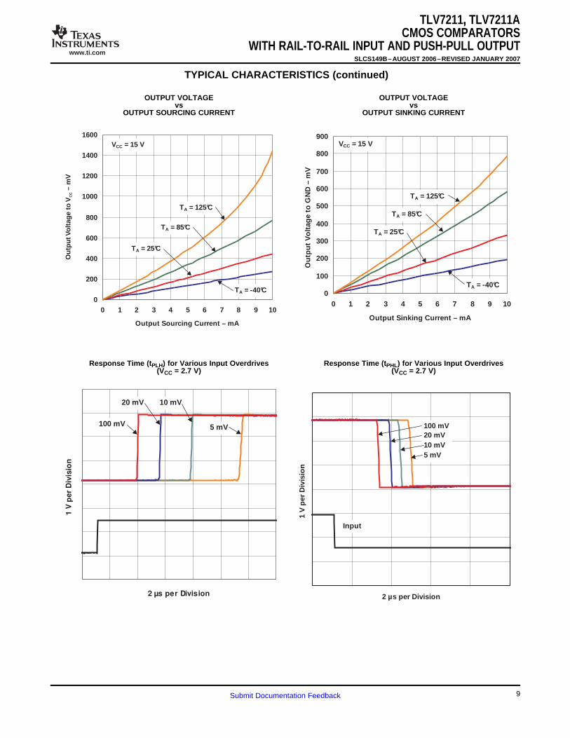
TYPICAL CHARACTERISTICS (continued)
OUTPUT SOURCING CURRENT OUTPUT SINKING CURRENTvs vs
SUPPLY VOLTAGE SUPPLY VOLTAGE
OUTPUT VOLTAGE OUTPUT VOLTAGEvs vs
OUTPUT SOURCING CURRENT OUTPUT SINKING CURRENT
8 Submit Documentation Feedback
www.ti.com
0
100
200
300
400
500
600
700
800
900
0 1 2 3 4 5 6 7 8 9 10
Output Sinking Current – mAO
utpu
tVol
tage
toG
ND
–m
V
VCC = 15 V
TA = -40°C
TA = 25°C
TA = 85°C
TA = 125°C
0
200
400
600
800
1000
1200
1400
1600
0 1 2 3 4 5 6 7 8 9 10
Output Sourcing Current – mA
Out
putV
olta
geto
VC
C–
mV
VCC = 15 V
TA = -40°C
TA = 25°C
TA = 85°C
TA = 125°C
Out
putV
olta
ge to
V–
mV
CC
2 µs per Division
1V
per
Div
isio
n
20 mV
100 mV 5 mV
10 mV
2 µs per Division
1V
perD
ivis
ion
100 mV20 mV10 mV5 mV
Input
TLV7211,, TLV7211ACMOS COMPARATORS
WITH RAIL-TO-RAIL INPUT AND PUSH-PULL OUTPUTSLCS149B–AUGUST 2006–REVISED JANUARY 2007
TYPICAL CHARACTERISTICS (continued)
OUTPUT VOLTAGE OUTPUT VOLTAGEvs vs
OUTPUT SOURCING CURRENT OUTPUT SINKING CURRENT
Response Time (tPLH) for Various Input Overdrives Response Time (tPHL) for Various Input Overdrives(VCC = 2.7 V) (VCC = 2.7 V)
9Submit Documentation Feedback

www.ti.com
2 µs per Division
1V
perD
ivis
ion
100 mV20 mV10 mV5 mV
Input
2 µs per Division
1V
perD
ivis
ion
100 mV20 mV10 mV5 mV
Input
2 µs per Division
3V
perD
ivis
ion
100 mV20 mV10 mV5 mV
Input
2 µs per Division
3V
perD
ivis
ion
100 mV20 mV10 mV5 mV
Input
TLV7211,, TLV7211ACMOS COMPARATORSWITH RAIL-TO-RAIL INPUT AND PUSH-PULL OUTPUTSLCS149B–AUGUST 2006–REVISED JANUARY 2007
TYPICAL CHARACTERISTICS (continued)
Response Time (tPLH) for Various Input Overdrives Response Time (tPHL) for Various Input Overdrives(VCC = 5 V) (VCC = 5 V)
Response Time (tPLH) for Various Input Overdrives Response Time (tPHL) for Various Input Overdrives(VCC = 15 V) (VCC = 15 V)
10 Submit Documentation Feedback

PACKAGE OPTION ADDENDUM
www.ti.com 10-Jun-2014
Addendum-Page 1
PACKAGING INFORMATION
Orderable Device Status(1)
Package Type PackageDrawing
Pins PackageQty
Eco Plan(2)
Lead/Ball Finish(6)
MSL Peak Temp(3)
Op Temp (°C) Device Marking(4/5)
Samples
TLV7211AID ACTIVE SOIC D 8 75 Green (RoHS& no Sb/Br)
CU NIPDAU Level-1-260C-UNLIM -40 to 85 7211AI
TLV7211AIDBVR ACTIVE SOT-23 DBV 5 3000 Green (RoHS& no Sb/Br)
CU NIPDAU Level-1-260C-UNLIM -40 to 85 YBNM
TLV7211AIDCKR ACTIVE SC70 DCK 6 3000 Green (RoHS& no Sb/Br)
CU NIPDAU Level-1-260C-UNLIM -40 to 85 Y8A
TLV7211AIDCKT ACTIVE SC70 DCK 6 250 Green (RoHS& no Sb/Br)
CU NIPDAU Level-1-260C-UNLIM -40 to 85 Y8A
TLV7211AIDR ACTIVE SOIC D 8 2500 Green (RoHS& no Sb/Br)
CU NIPDAU Level-1-260C-UNLIM -40 to 85 7211AI
TLV7211ID ACTIVE SOIC D 8 75 Green (RoHS& no Sb/Br)
CU NIPDAU Level-1-260C-UNLIM -40 to 85 TY7211
TLV7211IDBVR ACTIVE SOT-23 DBV 5 3000 Green (RoHS& no Sb/Br)
CU NIPDAU Level-1-260C-UNLIM -40 to 85 YBKM
TLV7211IDCKR ACTIVE SC70 DCK 6 3000 Green (RoHS& no Sb/Br)
CU NIPDAU Level-1-260C-UNLIM -40 to 85 Y7A
TLV7211IDCKT ACTIVE SC70 DCK 6 250 Green (RoHS& no Sb/Br)
CU NIPDAU Level-1-260C-UNLIM -40 to 85 Y7A
TLV7211IDR ACTIVE SOIC D 8 2500 Green (RoHS& no Sb/Br)
CU NIPDAU Level-1-260C-UNLIM -40 to 85 TY7211
(1) The marketing status values are defined as follows:ACTIVE: Product device recommended for new designs.LIFEBUY: TI has announced that the device will be discontinued, and a lifetime-buy period is in effect.NRND: Not recommended for new designs. Device is in production to support existing customers, but TI does not recommend using this part in a new design.PREVIEW: Device has been announced but is not in production. Samples may or may not be available.OBSOLETE: TI has discontinued the production of the device.
(2) Eco Plan - The planned eco-friendly classification: Pb-Free (RoHS), Pb-Free (RoHS Exempt), or Green (RoHS & no Sb/Br) - please check http://www.ti.com/productcontent for the latest availabilityinformation and additional product content details.TBD: The Pb-Free/Green conversion plan has not been defined.Pb-Free (RoHS): TI's terms "Lead-Free" or "Pb-Free" mean semiconductor products that are compatible with the current RoHS requirements for all 6 substances, including the requirement thatlead not exceed 0.1% by weight in homogeneous materials. Where designed to be soldered at high temperatures, TI Pb-Free products are suitable for use in specified lead-free processes.Pb-Free (RoHS Exempt): This component has a RoHS exemption for either 1) lead-based flip-chip solder bumps used between the die and package, or 2) lead-based die adhesive used betweenthe die and leadframe. The component is otherwise considered Pb-Free (RoHS compatible) as defined above.Green (RoHS & no Sb/Br): TI defines "Green" to mean Pb-Free (RoHS compatible), and free of Bromine (Br) and Antimony (Sb) based flame retardants (Br or Sb do not exceed 0.1% by weightin homogeneous material)

PACKAGE OPTION ADDENDUM
www.ti.com 10-Jun-2014
Addendum-Page 2
(3) MSL, Peak Temp. - The Moisture Sensitivity Level rating according to the JEDEC industry standard classifications, and peak solder temperature.
(4) There may be additional marking, which relates to the logo, the lot trace code information, or the environmental category on the device.
(5) Multiple Device Markings will be inside parentheses. Only one Device Marking contained in parentheses and separated by a "~" will appear on a device. If a line is indented then it is a continuationof the previous line and the two combined represent the entire Device Marking for that device.
(6) Lead/Ball Finish - Orderable Devices may have multiple material finish options. Finish options are separated by a vertical ruled line. Lead/Ball Finish values may wrap to two lines if the finishvalue exceeds the maximum column width.
Important Information and Disclaimer:The information provided on this page represents TI's knowledge and belief as of the date that it is provided. TI bases its knowledge and belief on informationprovided by third parties, and makes no representation or warranty as to the accuracy of such information. Efforts are underway to better integrate information from third parties. TI has taken andcontinues to take reasonable steps to provide representative and accurate information but may not have conducted destructive testing or chemical analysis on incoming materials and chemicals.TI and TI suppliers consider certain information to be proprietary, and thus CAS numbers and other limited information may not be available for release.
In no event shall TI's liability arising out of such information exceed the total purchase price of the TI part(s) at issue in this document sold by TI to Customer on an annual basis.

TAPE AND REEL INFORMATION
*All dimensions are nominal
Device PackageType
PackageDrawing
Pins SPQ ReelDiameter
(mm)
ReelWidth
W1 (mm)
A0(mm)
B0(mm)
K0(mm)
P1(mm)
W(mm)
Pin1Quadrant
TLV7211AIDBVR SOT-23 DBV 5 3000 178.0 9.0 3.3 3.2 1.4 4.0 8.0 Q3
TLV7211AIDCKR SC70 DCK 6 3000 180.0 8.4 2.41 2.41 1.2 4.0 8.0 Q3
TLV7211AIDCKT SC70 DCK 6 250 180.0 8.4 2.41 2.41 1.2 4.0 8.0 Q3
TLV7211AIDR SOIC D 8 2500 330.0 12.4 6.4 5.2 2.1 8.0 12.0 Q1
TLV7211IDBVR SOT-23 DBV 5 3000 178.0 9.0 3.23 3.17 1.37 4.0 8.0 Q3
TLV7211IDCKR SC70 DCK 6 3000 180.0 8.4 2.41 2.41 1.2 4.0 8.0 Q3
TLV7211IDCKT SC70 DCK 6 250 180.0 8.4 2.41 2.41 1.2 4.0 8.0 Q3
TLV7211IDR SOIC D 8 2500 330.0 12.4 6.4 5.2 2.1 8.0 12.0 Q1
PACKAGE MATERIALS INFORMATION
www.ti.com 3-Aug-2017
Pack Materials-Page 1

*All dimensions are nominal
Device Package Type Package Drawing Pins SPQ Length (mm) Width (mm) Height (mm)
TLV7211AIDBVR SOT-23 DBV 5 3000 180.0 180.0 18.0
TLV7211AIDCKR SC70 DCK 6 3000 202.0 201.0 28.0
TLV7211AIDCKT SC70 DCK 6 250 202.0 201.0 28.0
TLV7211AIDR SOIC D 8 2500 340.5 338.1 20.6
TLV7211IDBVR SOT-23 DBV 5 3000 180.0 180.0 18.0
TLV7211IDCKR SC70 DCK 6 3000 202.0 201.0 28.0
TLV7211IDCKT SC70 DCK 6 250 202.0 201.0 28.0
TLV7211IDR SOIC D 8 2500 340.5 338.1 20.6
PACKAGE MATERIALS INFORMATION
www.ti.com 3-Aug-2017
Pack Materials-Page 2


www.ti.com
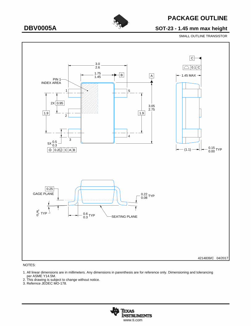
PACKAGE OUTLINE
C
TYP0.220.08
0.25
3.02.6
2X 0.95
1.9
1.45 MAX
TYP0.150.00
5X 0.50.3
TYP0.60.3
TYP80
1.9
A
3.052.75
B1.751.45
(1.1)
SOT-23 - 1.45 mm max heightDBV0005ASMALL OUTLINE TRANSISTOR
4214839/C 04/2017
NOTES: 1. All linear dimensions are in millimeters. Any dimensions in parenthesis are for reference only. Dimensioning and tolerancing per ASME Y14.5M.2. This drawing is subject to change without notice.3. Refernce JEDEC MO-178.
0.2 C A B
1
34
5
2
INDEX AREAPIN 1
GAGE PLANE
SEATING PLANE
0.1 C
SCALE 4.000

www.ti.com
EXAMPLE BOARD LAYOUT
0.07 MAXARROUND
0.07 MINARROUND
5X (1.1)
5X (0.6)
(2.6)
(1.9)
2X (0.95)
(R0.05) TYP
4214839/C 04/2017
SOT-23 - 1.45 mm max heightDBV0005ASMALL OUTLINE TRANSISTOR
NOTES: (continued) 4. Publication IPC-7351 may have alternate designs. 5. Solder mask tolerances between and around signal pads can vary based on board fabrication site.
SYMM
LAND PATTERN EXAMPLEEXPOSED METAL SHOWN
SCALE:15X
PKG
1
3 4
5
2
SOLDER MASKOPENINGMETAL UNDER
SOLDER MASK
SOLDER MASKDEFINED
EXPOSED METAL
METALSOLDER MASKOPENING
NON SOLDER MASKDEFINED
(PREFERRED)
SOLDER MASK DETAILS
EXPOSED METAL

www.ti.com
EXAMPLE STENCIL DESIGN
(2.6)
(1.9)
2X(0.95)
5X (1.1)
5X (0.6)
(R0.05) TYP
SOT-23 - 1.45 mm max heightDBV0005ASMALL OUTLINE TRANSISTOR
4214839/C 04/2017
NOTES: (continued) 6. Laser cutting apertures with trapezoidal walls and rounded corners may offer better paste release. IPC-7525 may have alternate design recommendations. 7. Board assembly site may have different recommendations for stencil design.
SOLDER PASTE EXAMPLEBASED ON 0.125 mm THICK STENCIL
SCALE:15X
SYMM
PKG
1
3 4
5
2


IMPORTANT NOTICE
Texas Instruments Incorporated (TI) reserves the right to make corrections, enhancements, improvements and other changes to itssemiconductor products and services per JESD46, latest issue, and to discontinue any product or service per JESD48, latest issue. Buyersshould obtain the latest relevant information before placing orders and should verify that such information is current and complete.TI’s published terms of sale for semiconductor products (http://www.ti.com/sc/docs/stdterms.htm) apply to the sale of packaged integratedcircuit products that TI has qualified and released to market. Additional terms may apply to the use or sale of other types of TI products andservices.Reproduction of significant portions of TI information in TI data sheets is permissible only if reproduction is without alteration and isaccompanied by all associated warranties, conditions, limitations, and notices. TI is not responsible or liable for such reproduceddocumentation. Information of third parties may be subject to additional restrictions. Resale of TI products or services with statementsdifferent from or beyond the parameters stated by TI for that product or service voids all express and any implied warranties for theassociated TI product or service and is an unfair and deceptive business practice. TI is not responsible or liable for any such statements.Buyers and others who are developing systems that incorporate TI products (collectively, “Designers”) understand and agree that Designersremain responsible for using their independent analysis, evaluation and judgment in designing their applications and that Designers havefull and exclusive responsibility to assure the safety of Designers' applications and compliance of their applications (and of all TI productsused in or for Designers’ applications) with all applicable regulations, laws and other applicable requirements. Designer represents that, withrespect to their applications, Designer has all the necessary expertise to create and implement safeguards that (1) anticipate dangerousconsequences of failures, (2) monitor failures and their consequences, and (3) lessen the likelihood of failures that might cause harm andtake appropriate actions. Designer agrees that prior to using or distributing any applications that include TI products, Designer willthoroughly test such applications and the functionality of such TI products as used in such applications.TI’s provision of technical, application or other design advice, quality characterization, reliability data or other services or information,including, but not limited to, reference designs and materials relating to evaluation modules, (collectively, “TI Resources”) are intended toassist designers who are developing applications that incorporate TI products; by downloading, accessing or using TI Resources in anyway, Designer (individually or, if Designer is acting on behalf of a company, Designer’s company) agrees to use any particular TI Resourcesolely for this purpose and subject to the terms of this Notice.TI’s provision of TI Resources does not expand or otherwise alter TI’s applicable published warranties or warranty disclaimers for TIproducts, and no additional obligations or liabilities arise from TI providing such TI Resources. TI reserves the right to make corrections,enhancements, improvements and other changes to its TI Resources. TI has not conducted any testing other than that specificallydescribed in the published documentation for a particular TI Resource.Designer is authorized to use, copy and modify any individual TI Resource only in connection with the development of applications thatinclude the TI product(s) identified in such TI Resource. NO OTHER LICENSE, EXPRESS OR IMPLIED, BY ESTOPPEL OR OTHERWISETO ANY OTHER TI INTELLECTUAL PROPERTY RIGHT, AND NO LICENSE TO ANY TECHNOLOGY OR INTELLECTUAL PROPERTYRIGHT OF TI OR ANY THIRD PARTY IS GRANTED HEREIN, including but not limited to any patent right, copyright, mask work right, orother intellectual property right relating to any combination, machine, or process in which TI products or services are used. Informationregarding or referencing third-party products or services does not constitute a license to use such products or services, or a warranty orendorsement thereof. Use of TI Resources may require a license from a third party under the patents or other intellectual property of thethird party, or a license from TI under the patents or other intellectual property of TI.TI RESOURCES ARE PROVIDED “AS IS” AND WITH ALL FAULTS. TI DISCLAIMS ALL OTHER WARRANTIES ORREPRESENTATIONS, EXPRESS OR IMPLIED, REGARDING RESOURCES OR USE THEREOF, INCLUDING BUT NOT LIMITED TOACCURACY OR COMPLETENESS, TITLE, ANY EPIDEMIC FAILURE WARRANTY AND ANY IMPLIED WARRANTIES OFMERCHANTABILITY, FITNESS FOR A PARTICULAR PURPOSE, AND NON-INFRINGEMENT OF ANY THIRD PARTY INTELLECTUALPROPERTY RIGHTS. TI SHALL NOT BE LIABLE FOR AND SHALL NOT DEFEND OR INDEMNIFY DESIGNER AGAINST ANY CLAIM,INCLUDING BUT NOT LIMITED TO ANY INFRINGEMENT CLAIM THAT RELATES TO OR IS BASED ON ANY COMBINATION OFPRODUCTS EVEN IF DESCRIBED IN TI RESOURCES OR OTHERWISE. IN NO EVENT SHALL TI BE LIABLE FOR ANY ACTUAL,DIRECT, SPECIAL, COLLATERAL, INDIRECT, PUNITIVE, INCIDENTAL, CONSEQUENTIAL OR EXEMPLARY DAMAGES INCONNECTION WITH OR ARISING OUT OF TI RESOURCES OR USE THEREOF, AND REGARDLESS OF WHETHER TI HAS BEENADVISED OF THE POSSIBILITY OF SUCH DAMAGES.Unless TI has explicitly designated an individual product as meeting the requirements of a particular industry standard (e.g., ISO/TS 16949and ISO 26262), TI is not responsible for any failure to meet such industry standard requirements.Where TI specifically promotes products as facilitating functional safety or as compliant with industry functional safety standards, suchproducts are intended to help enable customers to design and create their own applications that meet applicable functional safety standardsand requirements. Using products in an application does not by itself establish any safety features in the application. Designers mustensure compliance with safety-related requirements and standards applicable to their applications. Designer may not use any TI products inlife-critical medical equipment unless authorized officers of the parties have executed a special contract specifically governing such use.Life-critical medical equipment is medical equipment where failure of such equipment would cause serious bodily injury or death (e.g., lifesupport, pacemakers, defibrillators, heart pumps, neurostimulators, and implantables). Such equipment includes, without limitation, allmedical devices identified by the U.S. Food and Drug Administration as Class III devices and equivalent classifications outside the U.S.TI may expressly designate certain products as completing a particular qualification (e.g., Q100, Military Grade, or Enhanced Product).Designers agree that it has the necessary expertise to select the product with the appropriate qualification designation for their applicationsand that proper product selection is at Designers’ own risk. Designers are solely responsible for compliance with all legal and regulatoryrequirements in connection with such selection.Designer will fully indemnify TI and its representatives against any damages, costs, losses, and/or liabilities arising out of Designer’s non-compliance with the terms and provisions of this Notice.
Mailing Address: Texas Instruments, Post Office Box 655303, Dallas, Texas 75265Copyright © 2018, Texas Instruments Incorporated


![Hydrophobic interaction and hydrogen-bond network for a ...0 2 4 6 8 10 [au] simulation time [ps]-0.04-0.02 0 0.02 0.04 0.06 0.08 0 0.2 0.4 0.6 0.8 1 constraint force [au] simulation](https://img.dokumen.tips/doc/110x75/5f0ba34f7e708231d4317cb3/hydrophobic-interaction-and-hydrogen-bond-network-for-a-0-2-4-6-8-10-au-simulation.jpg)


![[XLS] · Web view0.01 734179 0.02 734195 0.04 701523 819832 0.02 720983 0.02 770833 2.5000000000000001E-3 819816 770841 5.0000000000000001E-3 819824 821624 720734 5.0000000000000001E-3](https://img.dokumen.tips/doc/110x75/5aa445417f8b9a185d8bc7e2/xls-view001-734179-002-734195-004-701523-819832-002-720983-002-770833-25000000000000001e-3.jpg)