Embed Size (px)
Citation preview

SCL
SDA
RESET
A0-A3
VDD
OUT15
OUT0
GND
TLC59116F
µC
3.3V or 5V
VLED
Product
Folder
Sample &Buy
Technical
Documents
Tools &
Software
Support &Community
TLC59116FSCLS714C –MARCH 2009–REVISED SEPTEMBER 2015
TLC59116F 16-Channel Fast-Mode Plus I2C Bus LED Driver1 Features • Active-Low Reset
• Supports Hot Insertion1• 16 LED Drivers (Each Output Programmable at
OFF, ON, LED Brightness, and Group • Low Standby CurrentDimming/Blinking Mixed With Individual LED • 3.3-V or 5-V Supply VoltageBrightness) • 5.5-V Tolerant Inputs
• 16 Open-Drain Output Channels • 28-Pin TSSOP (PW)• 256-Step (8-Bit) Linear Programmable Brightness • –40°C to 85°C Operation
Per LED Output Varying From Fully OFF (Default)to Maximum Brightness Using a 97-kHz PWM 2 ApplicationsSignal
• Gaming• 256-Step Group Brightness Control Allows• Small SignageGeneral Dimming (Using a 190-Hz PWM Signal• Industrial EquipmentFrom Fully OFF to Maximum Brightness (Default)
• 256-Step Group Blinking With Frequency3 DescriptionProgrammable From 24 Hz to 10.73 s and DutyThe TLC59116F is an I2C-bus controlled 16-channelCycle from 0% to 99.6%LED driver optimized for red/green/blue/amber• Four Hardware Address Pins Allow 14 (RGBA) color mixing applications. Each LED outputTLC59116F Devices to be Connected to the has its own 8-bit resolution (256 steps) fixed
Same I2C Bus frequency individual PWM controller that operates at• Four Software-Programmable I2C Bus Addresses 97 kHz with a duty cycle that is adjustable from 0% to
99.6% to allow the LED to be set to a specific(One LED Group Call Address and Three LEDbrightness value. An additional 8-bit resolution (256Sub-Call Addresses) Allow Groups of Devices tosteps) group PWM controller has both a fixedbe Addressed Simultaneously in Any Combinationfrequency of 190 Hz and an adjustable frequency(For example, One Register Used for 'All Call' Sobetween 24 Hz to once every 10.73 seconds with aAll the TLC59116Fs on the I2C Bus Can be duty cycle that is adjustable from 0% to 99.6% that isAddressed at the Same Time and the Second used to either dim or blink all LEDs with the sameRegister Used for Three Different Addresses So value.
That 1/3 of all Devices on the Bus Can BeAddressed at the Same Time in a Group). Device Information (1)
Software Enable and Disable for I2C Bus Address. PART NUMBER PACKAGE BODY SIZE (NOM)• Software Reset Feature (SWRST Call) Allows the TSSOP (28) 9.70 mm × 4.40 mm
TLC59116FDevice to be Reset Through the I2C Bus VQFN (32) 5.00 mm × 5.00 mm• Up to 14 Possible Hardware Adjustable Individual (1) For all available packages, see the orderable addendum at
I2C Bus Addresses Per Device so That Each the end of the datasheet.Device Can be Programmed
Application Schematic• Output State Change Programmable on theAcknowledge or the STOP Command to UpdateOutputs Byte-by-Byte or All at the Same Time(Default to Change on STOP).
• 120-mA Maximum Output Current• 17-V Maximum Output Voltage• 25-MHz Internal Oscillator Requires No External
Components• 1-MHz Fast-Mode Plus (FM+) Compatible I2C Bus
Interface With 30 mA High Drive Capability onSDA Output for Driving High Capacity Buses
• Internal Power-On Reset• Noise Filter on SCL/SDA Inputs• No Glitch on Power Up1
An IMPORTANT NOTICE at the end of this data sheet addresses availability, warranty, changes, use in safety-critical applications,intellectual property matters and other important disclaimers. PRODUCTION DATA.
TLC59116FSCLS714C –MARCH 2009–REVISED SEPTEMBER 2015 www.ti.com
Table of Contents8.3 Feature Description................................................. 101 Features .................................................................. 18.4 Device Functional Modes........................................ 112 Applications ........................................................... 18.5 Programming........................................................... 113 Description ............................................................. 18.6 Register Maps ......................................................... 164 Revision History..................................................... 2
9 Application and Implementation ........................ 235 Pin Configuration and Functions ......................... 39.1 Application Information............................................ 236 Specifications......................................................... 49.2 Typical Application ................................................. 246.1 Absolute Maximum Ratings ..................................... 4
10 Power Supply Recommendations ..................... 266.2 ESD Ratings.............................................................. 411 Layout................................................................... 266.3 Recommended Operating Conditions ...................... 4
11.1 Layout Guidelines ................................................. 266.4 Thermal Information .................................................. 411.2 Layout Examples................................................... 266.5 Electrical Characteristics........................................... 5
12 Device and Documentation Support ................. 286.6 I2C Interface Bus Timing Requirements ................... 612.1 Community Resources.......................................... 286.7 Typical Characteristics .............................................. 712.2 Trademarks ........................................................... 287 Parameter Measurement Information .................. 712.3 Electrostatic Discharge Caution............................ 288 Detailed Description .............................................. 912.4 Glossary ................................................................ 288.1 Overview ................................................................... 9
13 Mechanical, Packaging, and Orderable8.2 Functional Block Diagram ......................................... 9Information ........................................................... 28
4 Revision HistoryNOTE: Page numbers for previous revisions may differ from page numbers in the current version.
Changes from Revision B (July 2011) to Revision C Page
• Added Pin Configuration and Functions section, ESD Ratings table, Feature Description section, Device FunctionalModes, Application and Implementation section, Power Supply Recommendations section, Layout section, Deviceand Documentation Support section, and Mechanical, Packaging, and Orderable Information section .............................. 1
• Removed Thermal Impedence table from Specifications ...................................................................................................... 5• Added Figure 1 and Figure 2 to Typical Characteristics ....................................................................................................... 6• Removed Figure 9 from Control Register............................................................................................................................. 16• Added Figure 22 and Figure 23 to Layout Examples .......................................................................................................... 26
Changes from Revision A (June 2010) to Revision B Page
• Changed QFN PIN NO. to fix pin assignment typo. ............................................................................................................... 3
2 Submit Documentation Feedback Copyright © 2009–2015, Texas Instruments Incorporated
Product Folder Links: TLC59116F

24
20
23
19
22
18
21
17
RESETGND
GND
OUT15
OUT14
OUT13
OUT12
OUT11
32
28
31
27
30
26
29
25
A1
A0
SD
A
N.C
.
N.C
.
N.C
.V
CC
SC
L
9 13
10
14
11
15
12
16
OU
T5
OU
T6
OU
T9
OU
T7
N.C
.
N.C
.
OU
T8
OU
T10
1
5
2
6
3
7
4
8
A2A3
GND
OUT0
OUT1
OUT2
OUT3
OUT4
ExposedThermal Pad
20
26
28
19
25
27
18
24
17
23
16
22
15
21
1
2
3
4
5
6
7
14
8
13
9
12
10
11
OUT0
OUT4
OUT1
OUT5
OUT2
OUT6
OUT3
OUT7
A0
A1
GND
A2
A3
N.C.
RESET
OUT11
OUT10
OUT9
OUT15
OUT13
OUT8
OUT14
OUT12
VCC
GND
GND
SDA
SCL
TLC59116Fwww.ti.com SCLS714C –MARCH 2009–REVISED SEPTEMBER 2015
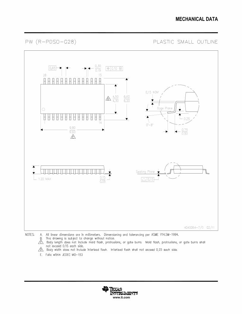
5 Pin Configuration and Functions
PW Package RHB Package28-Pin TSSOP 32-Pin VQFN
Top View Top View
If used, the exposed thermal pad must be connected as a secondary ground.N.C. – No internal connection
Pin FunctionsPIN
I/O DESCRIPTIONNAME QFN (RHB) TSSOP (PW)
A0 31 2 I Address input 0A1 32 3 I Address input 1A2 1 4 I Address input 2A3 2 5 I Address input 3GND 7, 18, 23 10, 19, 24 – Power groundN.C. 12, 13, 28, 29, 30 1 – No internal connectionOUT0OUT1
3–6 6–9 O Open-drain output 0 to 3, LED ON at lowOUT2OUT3OUT4OUT5
8–11 11–14 O Open-drain output 4 to 7, LED ON at lowOUT6OUT7OUT8OUT9
14–17 15–18 O Open-drain output 8 to 11, LED ON at lowOUT10OUT11OUT12OUT13
19–22 20–23 O Open-drain output 12 to 15, LED ON at lowOUT14OUT15RESET 24 25 I Active-low reset inputSCL 25 26 I Serial clock inputSDA 26 27 I/O Serial data input/outputVCC 27 28 – Power supply
Copyright © 2009–2015, Texas Instruments Incorporated Submit Documentation Feedback 3
Product Folder Links: TLC59116F

TLC59116FSCLS714C –MARCH 2009–REVISED SEPTEMBER 2015 www.ti.com
6 Specifications
6.1 Absolute Maximum Ratingsover operating free-air temperature range (unless otherwise noted) (see (1) )
MIN MAX UNITVCC Supply voltage 0 7 VVI Input voltage –0.4 7 VVO Output voltage –0.5 20 VIO Continuous output current per channel 120 mAPD Power dissipation (TA = 25°C, JESD 51-7) PW package 1.6 WTJ Junction temperature –40 150 °CTstg Storage temperature –55 150 °C
(1) Stresses beyond those listed under Absolute Maximum Ratings may cause permanent damage to the device. These are stress ratingsonly, which do not imply functional operation of the device at these or any other conditions beyond those indicated under RecommendedOperating Conditions . Exposure to absolute-maximum-rated conditions for extended periods may affect device reliability.
6.2 ESD RatingsVALUE UNIT
Human body model (HBM), per ANSI/ESDA/JEDEC JS-001 (1) ±1500ElectrostaticV(ESD) Vdischarge Charged-device model (CDM), per JEDEC specification JESD22-C101 (2) ±500
(1) JEDEC document JEP155 states that 500-V HBM allows safe manufacturing with a standard ESD control process.(2) JEDEC document JEP157 states that 250-V CDM allows safe manufacturing with a standard ESD control process.
6.3 Recommended Operating Conditionsover operating free-air temperature range (unless otherwise noted) (see (1))
MIN MAX UNITVCC Supply voltage 3 5.5 VVIH High-level input voltage SCL, SDA, RESET, A0, A1, A2, A3 VCC × 0.7 VCC VVIL Low-level input voltage SCL, SDA, RESET, A0, A1, A2, A3 0 VCC × 0.3 VVO Output voltage OUT0–OUT15 17 V
VCC = 3 V 20IOL Low-level output current SDA mA
VCC = 5 V 30IO Output current per channel OUT0–OUT15 120 mATA Operating free-air temperature –40 85 °C
(1) All unused inputs of the device must be held at VCC or GND to ensure proper device operation.
6.4 Thermal InformationTLC59116F
THERMAL METRIC (1) PW (TSSOP) RHB (VQFN) UNIT28 PINS 32 PINS
RθJA Junction-to-ambient thermal resistance 78 34.4 °C/WRθJC(top) Junction-to-case (top) thermal resistance 18.8 26.3 °C/WRθJB Junction-to-board thermal resistance 36 8.3 °C/WψJT Junction-to-top characterization parameter 0.5 0.4 °C/WψJB Junction-to-board characterization parameter 35.5 8.2 °C/WRθJC(bot) Junction-to-case (bottom) thermal resistance — 3.3 °C/W
(1) For more information about traditional and new thermal metrics, see the Semiconductor and IC Package Thermal Metrics applicationreport, SPRA953.
4 Submit Documentation Feedback Copyright © 2009–2015, Texas Instruments Incorporated
Product Folder Links: TLC59116F

TLC59116Fwww.ti.com SCLS714C –MARCH 2009–REVISED SEPTEMBER 2015
6.5 Electrical CharacteristicsVCC = 3 V to 5.5 V, TA = –40°C to 85°C (unless otherwise noted)
PARAMETER TEST CONDITIONS MIN TYP (1) MAX UNITSCL, SDA,Input/output leakageIL A0, A1, A2, A3, VI = VCC or GND ±0.3 µAcurrent RESET
Output leakage current OUT0–OUT15 VO = 17 V, TJ = 25°C 0.5 µAVPOR Power-on reset voltage 2.5 V
VCC = 3 V, VOL = 0.4 V 20Low-level outputIOL SDA mAcurrent VCC = 5 V, VOL = 0.4 V 30VCC = 3 V, IOL = 120 mA 200 450Low-level outputVOL OUT0–OUT15 mVvoltage VCC = 4.5 V, IOL = 120 mA 175 400VCC = 3 V, IOL = 120 mA 1.67 3.75
rON On resistance OUT0–OUT15 ΩVCC = 4.5 V, IOL = 120 mA 1.46 3.3
TSD Overtemperature shutdown (2) 150 175 200 °CTHYS Restart hysteresis 15 °CCi Input capacitance SCL, A0, A1, A2, A3, RESET VI = VCC or GND 5 pF
Input/outputCio SDA VI = VCC or GND 8 pFcapacitanceICC Supply current OUT0–OUT15 = OFF VCC = 5.5 V 13 mA
(1) All typical values are at TJ = 25°C.(2) Specified by design; not production tested.
Copyright © 2009–2015, Texas Instruments Incorporated Submit Documentation Feedback 5
Product Folder Links: TLC59116F

TLC59116FSCLS714C –MARCH 2009–REVISED SEPTEMBER 2015 www.ti.com
6.6 I2C Interface Bus Timing RequirementsTA = –40°C to 85°C
STANDARD-MODE FAST-MODE FAST-MODE PLUSI2C BUS I2C BUS I2C BUSPARAMETER UNIT
MIN MAX MIN MAX MIN MAXI2C InterfacefSCL SCL clock frequency 0 100 0 400 0 1000 kHz
Bus free time between a STOP andtBUF 4.7 1.3 0.5 µsSTART conditionHold time (repeated) STARTtHD;STA 4 0.6 0.26 µsconditionSet-up time for a (repeated) STARTtSU;STA 1.7 0.6 0.26 µscondition
tSU;STO Set-up time for STOP condition 4 0.6 0.26 µstHD;DAT Data hold time 0 0 0 nstVD;ACK Data valid acknowledge time (1) 0.3 3.45 0.1 0.9 0.05 0.45 µstVD;DAT Data valid time (2) 0.3 3.45 0.1 0.9 0.05 0.45 µstSU;DAT Data set-up time 250 100 50 nstLOW Low period of the SCL clock 4.7 1.3 0.5 µstHIGH High period of the SCL clock 4 0.6 0.26 µs
Fall times of both SDA and SCLtf 300 20 + 0.1Cb(5) 300 120 nssignals (3) (4)
Rise time of both SDA and SCLtr 1000 20 + 0.1Cb(5) 300 120 nssignals
Pulse width of spikes that must betSP 50 50 50 nssuppressed by the input filter (6)
ResettW Reset pulse width 10 10 10 nstREC Reset recovery time 0 0 0 nstRESET Time to reset (7) (8) 400 400 400 ns
(1) tVD;ACK = time for acknowledgment signal from SCL low to SDA (out) low.(2) tVD;DAT = minimum time for SDA data out to be valid following SCL low.(3) A master device must internally provide a hold time of at least 300 ns for the SDA signal (refer to the VIL of the SCL signal) in order to
bridge the undefined region of SCL's falling edge.(4) The maximum tf for the SDA and SCL bus lines is specified at 300 ns. The maximum fall time (tf) for the SDA output stage is specified
at 250 ns. This allows series protection resistors to be connected between the SDA and the SCL pins and the SDA/SCL bus lineswithout exceeding the maximum specified tf.
(5) Cb = total capacitance of one bus line in pF.(6) Input filters on the SDA and SCL inputs suppress noise spikes less than 50 ns.(7) Resetting the device while actively communicating on the bus may cause glitches or errant STOP conditions.(8) Upon reset, the full delay will be the sum of tRESET and the RC time constant of the SDA bus.
6 Submit Documentation Feedback Copyright © 2009–2015, Texas Instruments Incorporated
Product Folder Links: TLC59116F

ACK OR READ CYCLESTART
SCL
SDA
RESET
OUTx LED OFF
30% 30%
50%
50%50%50%
tREC
tRESET
tRESET
tW
0
2
4
6
8
10
12
3.0 3.5 4.0 4.5 5.0 5.5
I CC (
mA
)
VCC (V)
85°C
25°C
±40C
C001
0
10
20
30
40
50
60
70
0 100 200 300 400 500 600 700
LED
Cur
rent
(m
A)
RSET (
VF = 2 V
VF = 3 V
VF = 4 V
C002
TLC59116Fwww.ti.com SCLS714C –MARCH 2009–REVISED SEPTEMBER 2015
6.7 Typical Characteristics
All LEDs offAll LEDs on Duty Cycle = 100%
Figure 2. ICC vs VCC with LEDs OffFigure 1. ICC vs VCC with LEDs On
7 Parameter Measurement Information
Figure 3. Definition of RESET Timing
Copyright © 2009–2015, Texas Instruments Incorporated Submit Documentation Feedback 7
Product Folder Links: TLC59116F

RL
RTCL
VO
VCC
VI
Open
VCC
GND
PULSEGENERATOR DUT
SCL
SDA
Protocol
START
(S)Condition
Bit 7MSB(A7)
Bit 6(A6)
Bit 7(D1)
Bit 8(D0)
Acknowledge(A)
STOP Condition(P)
tBUF
tLOW 1/fSCL
tHD;STA TSU;STOtSU;DAT
tSU;STA
tHD;DAT tVD;DAT tVD;ACK
tHIGH
tf
tr
tBUF
tLOW
tHD;STA
tHD;STA
tSP
tSU;STO
tSU;STA
tSU;DATtHD;DAT tHIGH
tf
SCL
P SrS P
SDA
tr
TLC59116FSCLS714C –MARCH 2009–REVISED SEPTEMBER 2015 www.ti.com
Parameter Measurement Information (continued)
Figure 4. Definition of Timing
A. Rise and fall times refer to VIL and VIH.
Figure 5. I2C Bus Timing
A. Load resistor, RL, for SDA and SCL > 1 kΩ (3 mA or less current)B. Load capacitance, CL, includes jig and probe capacitanceC. Termination resistance, RT, should be equal to the output impedance ZO of the pulse generators.
Figure 6. Test Circuit for Switching Characteristics
8 Submit Documentation Feedback Copyright © 2009–2015, Texas Instruments Incorporated
Product Folder Links: TLC59116F
INPUT FILTER
I C BUS CONTROL2
GRPFREQREGISTER
POWER-ONRESET CONTROL
OUT0 OUT14OUT1 OUT15
25 MHOSCILLATOR
z
‘0’ – Permanently OFF‘1’ – Permanently ON
GND
VCC
RESET
SDA
SCL
190 Hz
24.3 Hk z97 Hk zGRPPWMREGISTER
PWM
REGISTERBRIGHTNESS
CONTROL
X
TLC59116F
LED STATESELECT
REGISTER
OUTPUT DRIVER
A1 A3A0 A2
TLC59116Fwww.ti.com SCLS714C –MARCH 2009–REVISED SEPTEMBER 2015
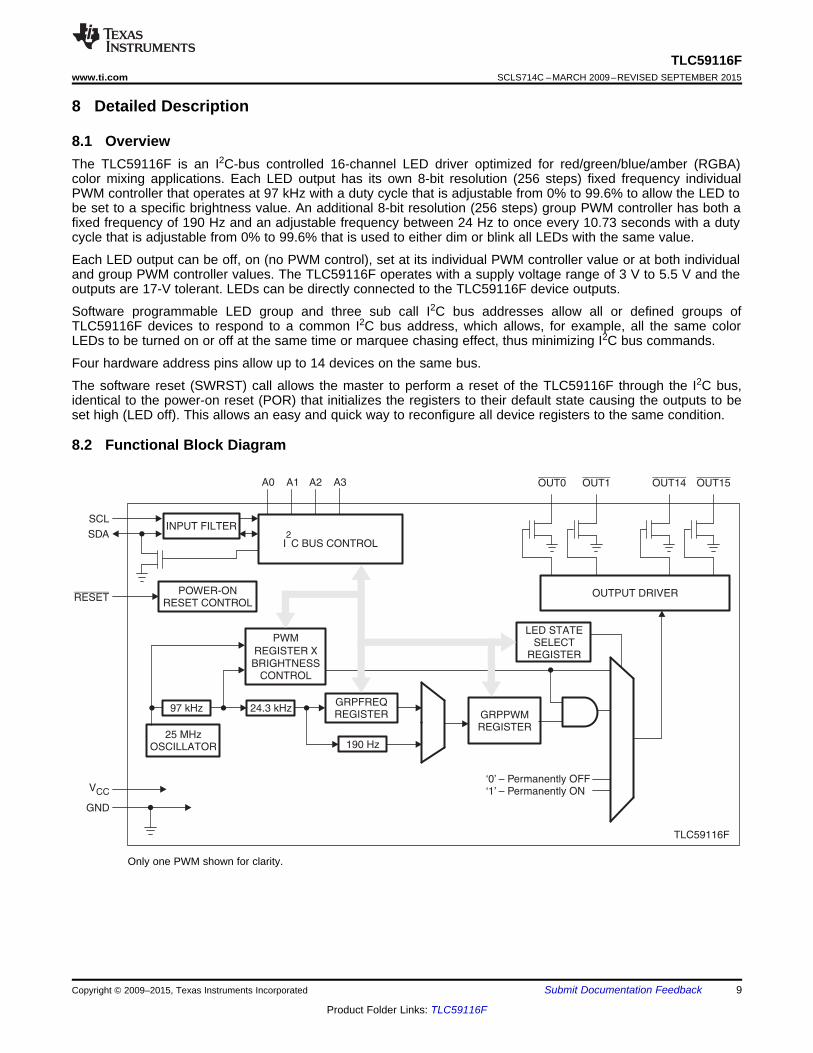
8 Detailed Description
8.1 OverviewThe TLC59116F is an I2C-bus controlled 16-channel LED driver optimized for red/green/blue/amber (RGBA)color mixing applications. Each LED output has its own 8-bit resolution (256 steps) fixed frequency individualPWM controller that operates at 97 kHz with a duty cycle that is adjustable from 0% to 99.6% to allow the LED tobe set to a specific brightness value. An additional 8-bit resolution (256 steps) group PWM controller has both afixed frequency of 190 Hz and an adjustable frequency between 24 Hz to once every 10.73 seconds with a dutycycle that is adjustable from 0% to 99.6% that is used to either dim or blink all LEDs with the same value.
Each LED output can be off, on (no PWM control), set at its individual PWM controller value or at both individualand group PWM controller values. The TLC59116F operates with a supply voltage range of 3 V to 5.5 V and theoutputs are 17-V tolerant. LEDs can be directly connected to the TLC59116F device outputs.
Software programmable LED group and three sub call I2C bus addresses allow all or defined groups ofTLC59116F devices to respond to a common I2C bus address, which allows, for example, all the same colorLEDs to be turned on or off at the same time or marquee chasing effect, thus minimizing I2C bus commands.
Four hardware address pins allow up to 14 devices on the same bus.
The software reset (SWRST) call allows the master to perform a reset of the TLC59116F through the I2C bus,identical to the power-on reset (POR) that initializes the registers to their default state causing the outputs to beset high (LED off). This allows an easy and quick way to reconfigure all device registers to the same condition.
8.2 Functional Block Diagram
Only one PWM shown for clarity.
Copyright © 2009–2015, Texas Instruments Incorporated Submit Documentation Feedback 9
Product Folder Links: TLC59116F

TLC59116FSCLS714C –MARCH 2009–REVISED SEPTEMBER 2015 www.ti.com
8.3 Feature Description
8.3.1 Power-On Reset (POR)When power is applied to VCC, an internal power-on reset holds the TLC59116F in a reset condition until VCCreaches VPOR. At this point, the reset condition is released and the TLC59116F registers and I2C bus statemachine are initialized to their default states causing all the channels to be deselected. Thereafter, VCC must belowered below 0.2 V to reset the device.
8.3.2 External ResetA reset can be accomplished by holding the RESET pin low for a minimum of tW. The TLC59116F registers andI2C state machine will be held in their default state until the RESET input is once again high.
This input requires a pullup resistor to VCC if no active connection is used.
8.3.3 Software ResetThe software reset call (SWRST Call) allows all the devices in the I2C bus to be reset to the power-up state valuethrough a specific formatted I2C bus command. To be performed correctly, it implies that the I2C bus is functionaland that there is no device hanging the bus.
The SWRST Call function is defined as the following:• A START command is sent by the I2C bus master.• The reserved SWRST I2C bus address '1101 011' with the R/W bit set to '0' (write) is sent by the I2C bus
master.• The TLC59116F device(s) acknowledge(s) after seeing the SWRST Call address '1101 0110' (D6h) only. If
the R/W bit is set to '1' (read), no acknowledge is returned to the I2C bus master.• Once the SWRST Call address has been sent and acknowledged, the master sends 2 bytes with 2 specific
values (SWRST data byte 1 and byte 2):a. Byte1 = A5h: the TLC59116F acknowledges this value only. If byte 1 is not equal to A5h, the TLC59116F
does not acknowledge it.b. Byte 2 = 5Ah: the TLC59116F acknowledges this value only. If byte 2 is not equal to 5Ah, the TLC59116F
does not acknowledge it.If more than 2 bytes of data are sent, the TLC59116F does not acknowledge any more.
• Once the right 2 bytes (SWRST data byte 1 and byte 2 only) have been sent and correctly acknowledged, themaster sends a STOP command to end the SWRST Call: the TLC59116F then resets to the default value(power-up value) and is ready to be addressed again within the specified bus free time (tBUF).
The I2C bus master must interpret a non-acknowledge from the TLC59116F (at any time) as a SWRST CallAbort. The TLC59116F does not initiate a reset of its registers. This happens only when the format of the STARTCall sequence is not correct.
8.3.4 Individual Brightness Control With Group Dimming/BlinkingA 97-kHz fixed frequency signal with programmable duty cycle (8 bits, 256 steps) is used to control individuallythe brightness for each LED.
On top of this signal, one of the following signals can be superimposed (this signal can be applied to the 4 LEDoutputs):• A lower 190-Hz fixed frequency signal with programmable duty cycle (8 bits, 256 steps) is used to provide a
global brightness control.• A programmable frequency signal from 24 Hz to 1/10.73 s (8 bits, 256 steps) is used to provide a global
blinking control.
10 Submit Documentation Feedback Copyright © 2009–2015, Texas Instruments Incorporated
Product Folder Links: TLC59116F
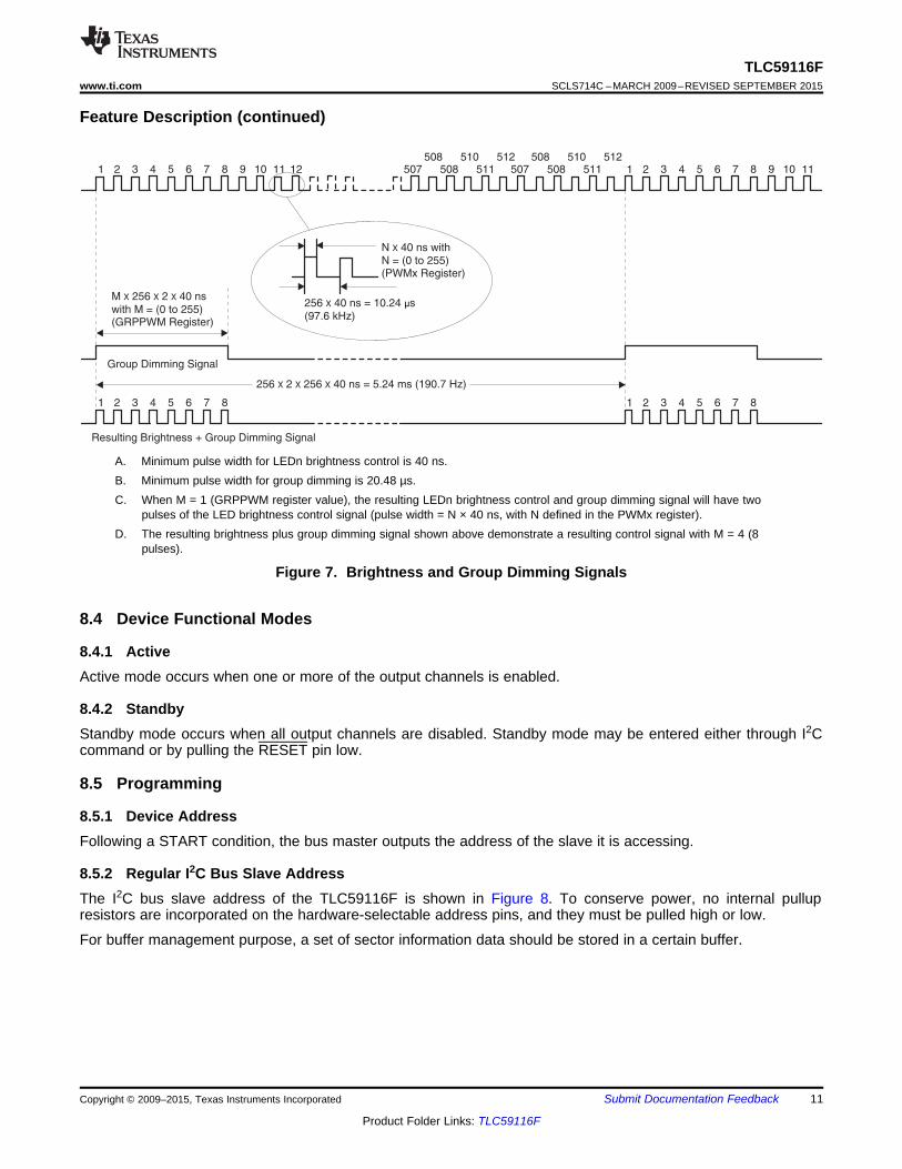
508 510 512 508 510 512
N 40 ns withN = (0 to 255)(PWMx Register)
X
256 40 ns = 10.24 s(97.6 kHz)
X µM 256 40 nswith M = (0 to 255)(GRPPWM Register)
X X X2
Group Dimming Signal
Resulting Brightness + Group Dimming Signal
1 2 3 4 5 6 7 8 9 10 11 1 2507 508 511 507 508 511 3 4 5 6 7 8 9 10 1112
1 2 3 4 5 6 7 8 1 2 3 4 5 6 7 8
256 256 40 ns = 5.24 ms (190.7 Hz)X X X2
TLC59116Fwww.ti.com SCLS714C –MARCH 2009–REVISED SEPTEMBER 2015
Feature Description (continued)
A. Minimum pulse width for LEDn brightness control is 40 ns.B. Minimum pulse width for group dimming is 20.48 µs.C. When M = 1 (GRPPWM register value), the resulting LEDn brightness control and group dimming signal will have two
pulses of the LED brightness control signal (pulse width = N × 40 ns, with N defined in the PWMx register).D. The resulting brightness plus group dimming signal shown above demonstrate a resulting control signal with M = 4 (8
pulses).
Figure 7. Brightness and Group Dimming Signals
8.4 Device Functional Modes
8.4.1 ActiveActive mode occurs when one or more of the output channels is enabled.
8.4.2 StandbyStandby mode occurs when all output channels are disabled. Standby mode may be entered either through I2Ccommand or by pulling the RESET pin low.
8.5 Programming
8.5.1 Device AddressFollowing a START condition, the bus master outputs the address of the slave it is accessing.
8.5.2 Regular I2C Bus Slave AddressThe I2C bus slave address of the TLC59116F is shown in Figure 8. To conserve power, no internal pullupresistors are incorporated on the hardware-selectable address pins, and they must be pulled high or low.
For buffer management purpose, a set of sector information data should be stored in a certain buffer.
Copyright © 2009–2015, Texas Instruments Incorporated Submit Documentation Feedback 11
Product Folder Links: TLC59116F
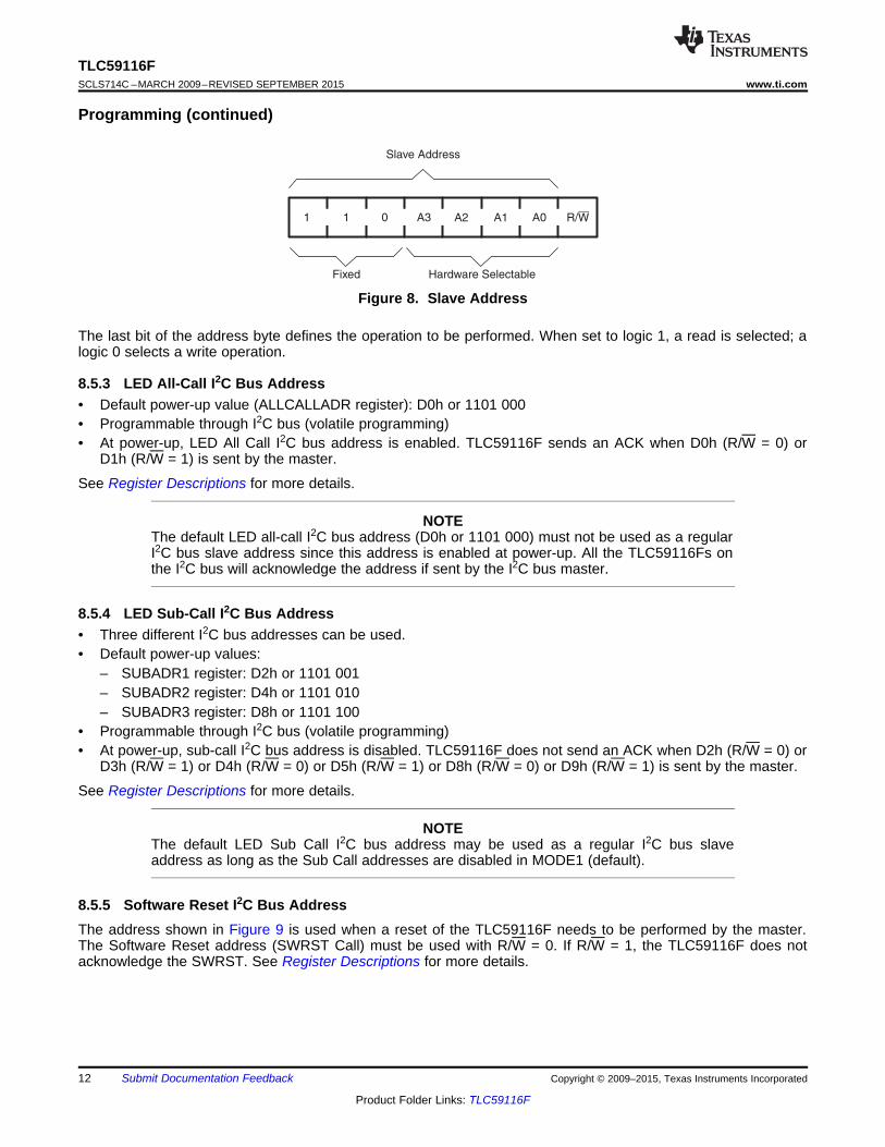
Slave Address
Hardware SelectableFixed
R/W1 1 0 A3 A2 A1 A0
TLC59116FSCLS714C –MARCH 2009–REVISED SEPTEMBER 2015 www.ti.com
Programming (continued)
Figure 8. Slave Address
The last bit of the address byte defines the operation to be performed. When set to logic 1, a read is selected; alogic 0 selects a write operation.
8.5.3 LED All-Call I2C Bus Address• Default power-up value (ALLCALLADR register): D0h or 1101 000• Programmable through I2C bus (volatile programming)• At power-up, LED All Call I2C bus address is enabled. TLC59116F sends an ACK when D0h (R/W = 0) or
D1h (R/W = 1) is sent by the master.
See Register Descriptions for more details.
NOTEThe default LED all-call I2C bus address (D0h or 1101 000) must not be used as a regularI2C bus slave address since this address is enabled at power-up. All the TLC59116Fs onthe I2C bus will acknowledge the address if sent by the I2C bus master.
8.5.4 LED Sub-Call I2C Bus Address• Three different I2C bus addresses can be used.• Default power-up values:
– SUBADR1 register: D2h or 1101 001– SUBADR2 register: D4h or 1101 010– SUBADR3 register: D8h or 1101 100
• Programmable through I2C bus (volatile programming)• At power-up, sub-call I2C bus address is disabled. TLC59116F does not send an ACK when D2h (R/W = 0) or
D3h (R/W = 1) or D4h (R/W = 0) or D5h (R/W = 1) or D8h (R/W = 0) or D9h (R/W = 1) is sent by the master.
See Register Descriptions for more details.
NOTEThe default LED Sub Call I2C bus address may be used as a regular I2C bus slaveaddress as long as the Sub Call addresses are disabled in MODE1 (default).
8.5.5 Software Reset I2C Bus AddressThe address shown in Figure 9 is used when a reset of the TLC59116F needs to be performed by the master.The Software Reset address (SWRST Call) must be used with R/W = 0. If R/W = 1, the TLC59116F does notacknowledge the SWRST. See Register Descriptions for more details.
12 Submit Documentation Feedback Copyright © 2009–2015, Texas Instruments Incorporated
Product Folder Links: TLC59116F

SCL SCL
START Condition STOP Condition
SDA SDA
PS
SCL
SDA
Data line stable;data valid
Change ofdata
allowed
0
R/W
1 1 0 1 0 1 1
TLC59116Fwww.ti.com SCLS714C –MARCH 2009–REVISED SEPTEMBER 2015
Programming (continued)
The software reset I2C bus address is reserved address and cannot be use as regular I2C bus slave address or as anLED All-Call or LED Sub-Call address.
Figure 9. Software Reset Address
8.5.6 Characteristics of the I2C BusThe I2C bus is for two-way, two-line communication between different ICs or modules. The two lines are a serialdata line (SDA) and a serial clock line (SCL). Both lines must be connected to a positive supply through a pullupresistor when connected to the output stages of a device. Data transfer may be initiated only when the bus is notbusy.
8.5.6.1 Bit TransferOne data bit is transferred during each clock pulse. The data on the SDA line must remain stable during the highperiod of the clock pulse as changes in the data line at this time will be interpreted as control signals (seeFigure 10).
Figure 10. Bit Transfer
8.5.6.2 START and STOP ConditionsBoth data and clock lines remain high when the bus is not busy. A high-to-low transition of the data line while theclock is high is defined as the START condition (S). A low-to-high transition of the data line while the clock ishigh is defined as the STOP condition (P) (see Figure 11).
Figure 11. Definition of START and STOP Conditions
Copyright © 2009–2015, Texas Instruments Incorporated Submit Documentation Feedback 13
Product Folder Links: TLC59116F

SCL From Master
Data OutputBy Receiver
Data OutputBy Transmitter
Not Acknowledge
Acknowledge
Clock Pulse forAcknowledgement
S
STARTCondition
1 2 8 9
SLAVE
MASTER
TRANSMITTER/
RECEIVER
SLAVE
RECEIVER
SLAVE
TRANSMITTER/
RECEIVER
MASTER
TRANSMITTER
MASTER
TRANSMITTER/
RECEIVER
SDA
SCL
I C BUS
MULTIPLEXER
2
TLC59116FSCLS714C –MARCH 2009–REVISED SEPTEMBER 2015 www.ti.com
Programming (continued)8.5.6.3 System ConfigurationA device generating a message is a transmitter; a device receiving is the receiver. The device that controls themessage is the master and the devices controlled by the master are the slaves (see Figure 12).
Figure 12. System Configuration
8.5.6.4 AcknowledgeThe number of data bytes transferred between the START and the STOP conditions from transmitter to receiveris not limited. Each byte of eight bits is followed by one acknowledge bit. The acknowledge bit is a high level puton the bus by the transmitter, whereas the master generates an extra acknowledge related clock pulse.
A slave receiver which is addressed must generate an acknowledge after the reception of each byte. Also amaster must generate an acknowledge after the reception of each byte that has been clocked out of the slavetransmitter. The device that acknowledges has to pull down the SDA line during the acknowledge clock pulse, sothat the SDA line is stable low during the high period of the acknowledge related clock pulse; set-up time andhold time must be taken into account.
A master receiver must signal an end of data to the transmitter by not generating an acknowledge on the lastbyte that has been clocked out of the slave. In this event, the transmitter must leave the data line high to enablethe master to generate a STOP condition.
Figure 13. Acknowledge on the I2C Bus
14 Submit Documentation Feedback Copyright © 2009–2015, Texas Instruments Incorporated
Product Folder Links: TLC59116F

Slave Address
AcknowledgeFrom Slave
AcknowledgeFrom Slave
AcknowledgeFrom Slave
AcknowledgeFrom Slave
Auto-Increment On
Auto-Increment onBrightness RegistersOnly
PWM RegisterSelection
START Condition
Control Register
R/W
A AS A6 A5 A2A3 A1 A0A4 A 10 00 1 0 0 1 0 A (cont.)
PWM1 RegisterPWM0 Register
AcknowledgeFrom Slave
AcknowledgeFrom Slave
PWM15 RegisterPWM14 Register
A A(cont.)
AcknowledgeFrom Slave
STOPCondition
PWMx Register
A P
AcknowledgeFrom Slave
PWM0 Register
A
AcknowledgeFrom Slave
AcknowledgeFrom Slave
STOPCondition
ALLCALLADR RegisterSUBADR3 Register
A A P(cont.)
Slave Address
AcknowledgeFrom Slave
AcknowledgeFrom Slave
AcknowledgeFrom Slave
AcknowledgeFrom Slave
Auto-Increment On
Auto-Increment onAll Registers
MODE1 RegisterSelection
START Condition
Control Register
R/W
S 1 1 A2A3 A1 A00 A 10 00 0 0 A A0 0 0 A (cont.)
MODE2 RegisterMODE1 Register
Slave Address
AcknowledgeFrom Slave
AcknowledgeFrom Slave
AcknowledgeFrom Slave
Auto-Increment Flag
Auto-Increment OptionsSTART Condition STOP
Condition
Control Register
R/W
S 1 1 A2A3 A1 A00 A X0 D3X X D4 PAD2 D1 D0 A
TLC59116Fwww.ti.com SCLS714C –MARCH 2009–REVISED SEPTEMBER 2015
Programming (continued)
Figure 14. Write to a Specific Register
Figure 15. Write to All Registers Using the Auto-Increment Feature
Figure 16. Multiple Writes to Individual Brightness Registers Only Using the Auto-Increment Feature
Copyright © 2009–2015, Texas Instruments Incorporated Submit Documentation Feedback 15
Product Folder Links: TLC59116F

Slave Address
AcknowledgeFrom Slave
AcknowledgeFrom Slave
AcknowledgeFrom Slave
STOPCondition
Auto-Increment Flag
ALLCALLADRRegister Selection
START Condition
Sequence A
Control Register
R/W
S A6 1A5 0A2 0A3 1A1 1A0 XA4 1A X 10 A1X X 1 P0 1 1 A
New LED All-Call I C Address2 (B)
AcknowledgeFrom Slave
AcknowledgeFrom the 4 Devices
AcknowledgeFrom Slave
STOPCondition
Auto-Increment Flag
LEDOUT0 Register SelectionSTART Condition
Sequence B
Control Register
R/W
S 1 11 01 11 00 01 10 1A X 00 A0X X 1 P1 0 0 A
The 16 LEDs are ON at AcknowledgeLEDOUT0 Register (LED0–LED3 Fully ON)
(C)
LED All-Call I C Address2
Slave Address
AcknowledgeFrom Slave
AcknowledgeFrom Slave
AcknowledgeFrom Slave
AcknowledgeFrom Master
Auto-Increment On
Auto-Incrementon All Registers
MODE1RegisterSelection
START Condition
Control Register
R/W R/WRepeated Start
(cont.)
Data from MODE1 RegisterSlave Address
S A6 A6A5 A5A2 A2A3 A3A1 A1A0 A0A4 A4A 1 Sr0 100 0 0 A0 0 0 A A
(cont.)
AcknowledgeFrom Master
AcknowledgeFrom Master
Data from PWM0 RegisterData from MODE2 Register
A
P
(cont.)
AcknowledgeFrom Master
Data from MODE1 Register
A
AcknowledgeFrom Master
Data from ALLCALLADR Register
AA
Not AcknowledgeFrom Master
STOPCondition
Data from Last Read Byte
(cont.) A
TLC59116FSCLS714C –MARCH 2009–REVISED SEPTEMBER 2015 www.ti.com
Programming (continued)
Figure 17. Read All Registers With the Auto-Increment Feature
A. In this example, four TLC59116Fs are used with the same sequence sent to each.B. ALLCALL bit in MODE1 register is equal to 1 for this example.C. OCH bit in MODE2 register is equal to 1 for this example.
Figure 18. LED All-Call I2C Bus Address Programming and LED All-Call Sequence Example
8.6 Register Maps
8.6.1 Control RegisterFollowing the successful acknowledgment of the slave address, LED All Call address or LED Sub Call address,the bus master will send a byte to the TLC59116F, which will be stored in the Control register. The lowest 5 bitsare used as a pointer to determine which register will be accessed (D[4:0]). The highest three bits are used asAuto-Increment flag and Auto-Increment options (AI[2:0]).
16 Submit Documentation Feedback Copyright © 2009–2015, Texas Instruments Incorporated
Product Folder Links: TLC59116F

Register AddressAuto-Increment
Flag
Auto-Increment Options
A 1I AI0 D4 D3 D2 D1 D0A 2I
TLC59116Fwww.ti.com SCLS714C –MARCH 2009–REVISED SEPTEMBER 2015
Register Maps (continued)
Figure 19. Control Register
When the Auto-Increment flag is set (AI2 = logic 1), the five low order bits of the Control register areautomatically incremented after a read or write. This allows the user to program the registers sequentially. Fourdifferent types of Auto-Increment are possible, depending on AI1 and AI0 values.
Table 1. Auto-Increment Options (1)
AI2 AI1 AI0 PIN DESCRIPTION0 0 0 No auto-increment
Auto-increment for all registers. D[4:0] roll over to 0 0000 after the last1 0 0 register (1 1011) is accessed.Auto-increment for individual brightness registers only. D[4:0] roll over1 0 1 to 0 0010 after the last register (1 0001) is accessed.Auto-increment for global control registers only. D[4:0] roll over to 11 1 0 0010 after the last register (1 0011) is accessed.Auto-increment for individual and global control registers only. D[4:0]1 1 1 roll over to 0 0010 after the last register (1 0011) is accessed.
(1) Other combinations not shown in Table 1 (AI[2:0] = 001, 010 and 011) are reserved and must not beused for proper device operation.
AI[2:0] = 000 is used when the same register must be accessed several times during a single I2C buscommunication (for example, changing the brightness of a single LED). Data is overwritten each time the registeris accessed during a write operation.
AI[2:0] = 100 is used when all the registers must be sequentially accessed (for example, power-upprogramming).
AI[2:0] = 101 is used when the four LED drivers must be individually programmed with different values during thesame I2C bus communication (for example, changing color setting to another color setting).
AI[2:0] = 110 is used when the LED drivers must be globally programmed with different settings during the sameI2C bus communication (for example, global brightness or blinking change).
AI[2:0] = 111 is used when individually and global changes must be performed during the same I2C buscommunication (for example, changing color and global brightness at the same time).
Only the five least-significant bits (LSBs) D[4:0] are affected by the AI[2:0] bits.
When Control register is written, the register entry point determined by D[4:0] is the first register that will beaddressed (read or write operation), and can be anywhere between 0 0000 and 1 1011 (as defined in ). WhenAI[2] = 1, the Auto-Increment flag is set and the rollover value at which the point where the register incrementstops and goes to the next one is determined by AI[2:0]. See for rollover values. For example, if the Controlregister = 1111 0100 (F4h), then the register addressing sequence will be (in hex):
14 → … → 1B → 00 → … → 13 → 02 → … → 13 → 02 → …as long as the master keeps sending or reading data.
Copyright © 2009–2015, Texas Instruments Incorporated Submit Documentation Feedback 17
Product Folder Links: TLC59116F

TLC59116FSCLS714C –MARCH 2009–REVISED SEPTEMBER 2015 www.ti.com
8.6.2 Register Descriptions
Table 2. Register DescriptionsREGISTER NAME ACCESS (1) FUNCTIONNUMBER (HEX)
00 MODE1 R/W Mode register 101 MODE2 R/W Mode register 202 PWM0 R/W Brightness control LED003 PWM1 R/W Brightness control LED104 PWM2 R/W Brightness control LED205 PWM3 R/W Brightness control LED306 PWM4 R/W Brightness control LED407 PWM5 R/W Brightness control LED508 PWM6 R/W Brightness control LED609 PWM7 R/W Brightness control LED70A PWM8 R/W Brightness control LED80B PWM9 R/W Brightness control LED90C PWM10 R/W Brightness control LED100D PWM11 R/W Brightness control LED110E PWM12 R/W Brightness control LED120F PWM13 R/W Brightness control LED1310 PWM14 R/W Brightness control LED1411 PWM15 R/W Brightness control LED1512 GRPPWM R/W Group duty cycle control13 GRPFREQ R/W Group frequency14 LEDOUT0 R/W LED output state 015 LEDOUT1 R/W LED output state 116 LEDOUT2 R/W LED output state 217 LEDOUT3 R/W LED output state 318 SUBADR1 R/W I2C bus sub-address 119 SUBADR2 R/W I2C bus sub-address 21A SUBADR3 R/W I2C bus sub-address 31B ALLCALLADR R/W LED All Call I2C bus address
(1) R = read, W = write
18 Submit Documentation Feedback Copyright © 2009–2015, Texas Instruments Incorporated
Product Folder Links: TLC59116F

TLC59116Fwww.ti.com SCLS714C –MARCH 2009–REVISED SEPTEMBER 2015
8.6.2.1 Mode Register 1 (MODE1)
Table 3. MODE1 – Mode Register 1 (Address 00h) Bit DescriptionBIT SYMBOL ACCESS (1) VALUE DESCRIPTION
0 (2) Register auto-increment disabled7 AI2 R
1 Register auto-increment enabled0 (2) Auto-increment bit 1 = 0
6 AI1 R1 Auto-increment bit 1 = 10 (2) Auto-increment bit 0 = 0
5 AI0 R1 Auto-increment bit 0 = 10 Normal mode (3)
4 SLEEP R/W1 (2) Low-power mode. Oscillator off. (4)
0 (2) TLC59116F does not respond to I2C bus sub-address 1.3 SUB1 R/W
1 TLC59116F responds to I2C bus sub-address 1.0 (2) TLC59116F does not respond to I2C bus sub-address 2.
2 SUB2 R/W1 TLC59116F responds to I2C bus sub-address 2.0 (2) TLC59116F does not respond to I2C bus sub-address 3.
1 SUB3 R/W1 TLC59116F responds to I2C bus sub-address 3.0 TLC59116F does not respond to LED all-call I2C bus address.
0 ALLCALL R/W1 (2) TLC59116F responds to LED all-call I2C bus address.
(1) R = read, W = write(2) Default value(3) It takes 500 µs max for the oscillator to be up and running once SLEEP bit has been set from logic 1 to 0. Timings on LEDn outputs are
not guaranteed if PWMx, GRPPWM, or GRPFREQ registers are accessed within the 500-µs window.(4) No LED control including ON/OFF, blinking and dimming is possible when oscillator is off. Writing to the register during SLEEP mode
does not affect LED condition. It is needed to set the SLEEP bit to logic 0 when LED condition is required to change.
8.6.2.2 Mode Register 2 (MODE2)
Table 4. MODE2 – Mode Register 2 (Address 01h) Bit DescriptionBIT SYMBOL ACCESS (1) VALUE DESCRIPTION7:6 R 00 (2) Reserved
0 (2) Group control = dimming5 DMBLNK R/W
1 Group control = blinking4 R 0 (2) Reserved
0 (2) Outputs change on STOP command (3)3 OCH R/W
1 Outputs change on ACK2:0 R 000 (2) Reserved
(1) R = read, W = write(2) Default value(3) Change of the outputs at the STOP command allows synchronizing outputs of more than one TLC59116F. Applicable to registers from
02h (PWM0) to 17h (LEDOUT) only.
Copyright © 2009–2015, Texas Instruments Incorporated Submit Documentation Feedback 19
Product Folder Links: TLC59116F

GDC[7:0]
256
Duty cycle =
IDCx[7:0]
256
Duty cycle =
TLC59116FSCLS714C –MARCH 2009–REVISED SEPTEMBER 2015 www.ti.com
8.6.2.3 Individual Brightness Control (PWM0–PWM15) Registers
Table 5. PWM0–PWM15 – Individual Brightness Control Registers (Address 02h to 11h) Bit DescriptionADDRESS REGISTER BIT SYMBOL ACCESS (1) VALUE (2) DESCRIPTION
02h PWM0 7:0 IDC0[7:0] R/W 0000 0000 PWM0 individual duty cycle03h PWM1 7:0 IDC1[7:0] R/W 0000 0000 PWM1 individual duty cycle04h PWM2 7:0 IDC2[7:0] R/W 0000 0000 PWM2 individual duty cycle05h PWM3 7:0 IDC3[7:0] R/W 0000 0000 PWM3 individual duty cycle06h PWM4 7:0 IDC4[7:0] R/W 0000 0000 PWM4 individual duty cycle07h PWM5 7:0 IDC5[7:0] R/W 0000 0000 PWM5 individual duty cycle08h PWM6 7:0 IDC6[7:0] R/W 0000 0000 PWM6 individual duty cycle09h PWM7 7:0 IDC7[7:0] R/W 0000 0000 PWM7 individual duty cycle0Ah PWM8 7:0 IDC8[7:0] R/W 0000 0000 PWM8 individual duty cycle0Bh PWM9 7:0 IDC9[7:0] R/W 0000 0000 PWM9 individual duty cycle0Ch PWM10 7:0 IDC10[7:0] R/W 0000 0000 PWM10 individual duty cycle0Dh PWM11 7:0 IDC11[7:0] R/W 0000 0000 PWM11 individual duty cycle0Eh PWM12 7:0 IDC12[7:0] R/W 0000 0000 PWM12 individual duty cycle0Fh PWM13 7:0 IDC13[7:0] R/W 0000 0000 PWM13 individual duty cycle10h PWM14 7:0 IDC14[7:0] R/W 0000 0000 PWM14 individual duty cycle11h PWM15 7:0 IDC15[7:0] R/W 0000 0000 PWM15 individual duty cycle
(1) R = read, W = write(2) Default value
A 97-kHz fixed frequency signal is used for each output. Duty cycle is controlled through 256 linear steps from00h (0% duty cycle = LED output off) to FFh (99.6% duty cycle = LED output at maximum brightness). Applicableto LED outputs programmed with LDRx = 10 or 11 (LEDOUT0 to LEDOUT3 registers).
(1)
8.6.2.4 Group Duty Cycle Control (GRPPWM) Register
Table 6. GRPPWM – Group Duty Cycle Control Register (Address 12h) Bit DescriptionADDRESS REGISTER BIT SYMBOL ACCESS (1) VALUE (2) DESCRIPTION
12h GRPPWM 7:0 GDC0[7:0] R/W 1111 1111 GRPPWM register
(1) R = read, W = write(2) Default value
When DMBLNK bit (MODE2 register) is programmed with logic 0, a 190-Hz fixed frequency signal issuperimposed with the 97-kHz individual brightness control signal. GRPPWM is then used as a global brightnesscontrol allowing the LED outputs to be dimmed with the same value.
NOTEThe value in GRPFREQ has to be programmed to 00h when DMBLNK = 0.
General brightness for the 16 outputs is controlled through 256 linear steps from 00h (0% duty cycle = LEDoutput off) to FFh (99.6% duty cycle = maximum brightness). Applicable to LED outputs programmed with LDRx= 11 (LEDOUT0 to LEDOUT3 registers).
When DMBLNK bit is programmed with logic 1, GRPPWM and GRPFREQ registers define a global blinkingpattern, where GRPFREQ contains the blinking period (from 24 Hz to 10.73 s) and GRPPWM the duty cycle(ON/OFF ratio in percentages).
(2)
20 Submit Documentation Feedback Copyright © 2009–2015, Texas Instruments Incorporated
Product Folder Links: TLC59116F

GFRQ[7:0] + 1
24
Global blinking period = (s)
TLC59116Fwww.ti.com SCLS714C –MARCH 2009–REVISED SEPTEMBER 2015
8.6.2.5 Group Frequency (GRPFREQ) Register
Table 7. GRPFREQ – Group Frequency Register (Address 13h) Bit DescriptionADDRESS REGISTER BIT SYMBOL ACCESS (1) VALUE (2) DESCRIPTION
13h GRPFREQ 7:0 GFRQ[7:0] R/W 0000 0000 GRPFREQ register
(1) R = read, W = write(2) Default value
GRPFREQ is used to program the global blinking period when DMBLNK bit (MODE2 register) is equal to 1.
NOTEThe value in GRPFREQ must be programmed to 00h when DMBLNK = 0.
Applicable to LED output programmed with LDRx = 11 (LEDOUT0 to LEDOUT3 registers). Blinking period iscontrolled through 256 linear steps from 00h (41 ms, frequency 24 Hz) to FFh (10.73 s).
(3)
8.6.2.6 LED Driver Output State (LEDOUT0–LEDOUT3) Register
Table 8. LEDOUT0–LEDOUT3 – LED Driver Output State Registers (Address 14h–17h) Bit DescriptionADDRESS REGISTER BIT SYMBOL ACCESS (1) VALUE (2) DESCRIPTION
7:6 LDR3[1:0] R/W 00 LED3 output state control5:4 LDR2[1:0] R/W 00 LED2 output state control
14h LEDOUT03:2 LDR1[1:0] R/W 00 LED1 output state control1:0 LDR0[1:0] R/W 00 LED0 output state control7:6 LDR7[1:0] R/W 00 LED7 output state control5:4 LDR6[1:0] R/W 00 LED6 output state control
15h LEDOUT13:2 LDR5[1:0] R/W 00 LED5 output state control1:0 LDR4[1:0] R/W 00 LED4 output state control7:6 LDR11[1:0] R/W 00 LED11 output state control5:4 LDR10[1:0] R/W 00 LED10 output state control
16h LEDOUT23:2 LDR9[1:0] R/W 00 LED9 output state control1:0 LDR8[1:0] R/W 00 LED8 output state control7:6 LDR15[1:0] R/W 00 LED15 output state control5:4 LDR14[1:0] R/W 00 LED14 output state control
17h LEDOUT33:2 LDR13[1:0] R/W 00 LED13 output state control1:0 LDR12[1:0] R/W 00 LED12 output state control
(1) R = read, W = write(2) Default value
LDRx = 00 : LED driver x is off (default power-up state).
LDRx = 01 : LED driver x is fully on (individual brightness and group dimming/blinking not controlled).
LDRx = 10 : LED driver x is individual brightness can be controlled through its PWMx register.
LDRx = 11 : LED driver x is individual brightness and group dimming/blinking can be controlled through its PWMxregister and the GRPPWM registers.
Copyright © 2009–2015, Texas Instruments Incorporated Submit Documentation Feedback 21
Product Folder Links: TLC59116F
TLC59116FSCLS714C –MARCH 2009–REVISED SEPTEMBER 2015 www.ti.com
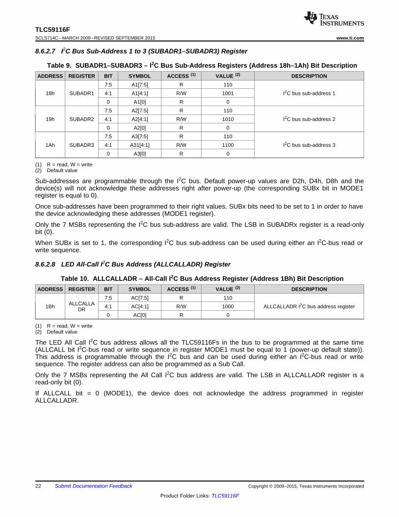
8.6.2.7 I2C Bus Sub-Address 1 to 3 (SUBADR1–SUBADR3) Register
Table 9. SUBADR1–SUBADR3 – I2C Bus Sub-Address Registers (Address 18h–1Ah) Bit DescriptionADDRESS REGISTER BIT SYMBOL ACCESS (1) VALUE (2) DESCRIPTION
7:5 A1[7:5] R 11018h SUBADR1 4:1 A1[4:1] R/W 1001 I2C bus sub-address 1
0 A1[0] R 07:5 A2[7:5] R 110
19h SUBADR2 4:1 A2[4:1] R/W 1010 I2C bus sub-address 20 A2[0] R 0
7:5 A3[7:5] R 1101Ah SUBADR3 4:1 A31[4:1] R/W 1100 I2C bus sub-address 3
0 A3[0] R 0
(1) R = read, W = write(2) Default value
Sub-addresses are programmable through the I2C bus. Default power-up values are D2h, D4h, D8h and thedevice(s) will not acknowledge these addresses right after power-up (the corresponding SUBx bit in MODE1register is equal to 0).
Once sub-addresses have been programmed to their right values, SUBx bits need to be set to 1 in order to havethe device acknowledging these addresses (MODE1 register).
Only the 7 MSBs representing the I2C bus sub-address are valid. The LSB in SUBADRx register is a read-onlybit (0).
When SUBx is set to 1, the corresponding I2C bus sub-address can be used during either an I2C-bus read orwrite sequence.
8.6.2.8 LED All-Call I2C Bus Address (ALLCALLADR) Register
Table 10. ALLCALLADR – All-Call I2C Bus Address Register (Address 1Bh) Bit DescriptionADDRESS REGISTER BIT SYMBOL ACCESS (1) VALUE (2) DESCRIPTION
7:5 AC[7:5] R 110ALLCALLA1Bh 4:1 AC[4:1] R/W 1000 ALLCALLADR I2C bus address registerDR
0 AC[0] R 0
(1) R = read, W = write(2) Default value
The LED All Call I2C bus address allows all the TLC59116Fs in the bus to be programmed at the same time(ALLCALL bit I2C-bus read or write sequence in register MODE1 must be equal to 1 (power-up default state)).This address is programmable through the I2C bus and can be used during either an I2C-bus read or writesequence. The register address can also be programmed as a Sub Call.
Only the 7 MSBs representing the All Call I2C bus address are valid. The LSB in ALLCALLADR register is aread-only bit (0).
If ALLCALL bit = 0 (MODE1), the device does not acknowledge the address programmed in registerALLCALLADR.
22 Submit Documentation Feedback Copyright © 2009–2015, Texas Instruments Incorporated
Product Folder Links: TLC59116F

TLC59116Fwww.ti.com SCLS714C –MARCH 2009–REVISED SEPTEMBER 2015
9 Application and Implementation
NOTEInformation in the following applications sections is not part of the TI componentspecification, and TI does not warrant its accuracy or completeness. TI’s customers areresponsible for determining suitability of components for their purposes. Customers shouldvalidate and test their design implementation to confirm system functionality.
9.1 Application InformationThis section highlights some of the design considerations for implementing this device in various applications.
9.1.1 Setting LED CurrentThe LED current is primarily dependent on the supply voltage, the forward voltage of the LED, and the seriesresistor (RSET). In many applications the supply voltage and LED forward voltage cannot be adjusted. Hence,RSET is utilized to adjust the LED current. This calculation is discussed in detail in the typical application example.
9.1.2 PWM Brightness DimmingThe perceived brightness of the LEDs can be adjusted by use of PWM dimming. For example, an LED driven at50% duty cycle will appear less bright than it would at 100% duty cycle. The TLC59116F offers duty cycle controlfor each individual channel and also offers group duty cycle control. Refer to the Register Map for detailsregarding programmable duty cycle.
Copyright © 2009–2015, Texas Instruments Incorporated Submit Documentation Feedback 23
Product Folder Links: TLC59116F
SCL
SDA
RESET
A0-A3
OUT14
VDD
OUT15
OUT13
OUT1
OUT0
GND
TLC59116F
SCL
SDA
RESET
Microcontroller
3.3V or 5V RSET
VLED
TLC59116FSCLS714C –MARCH 2009–REVISED SEPTEMBER 2015 www.ti.com
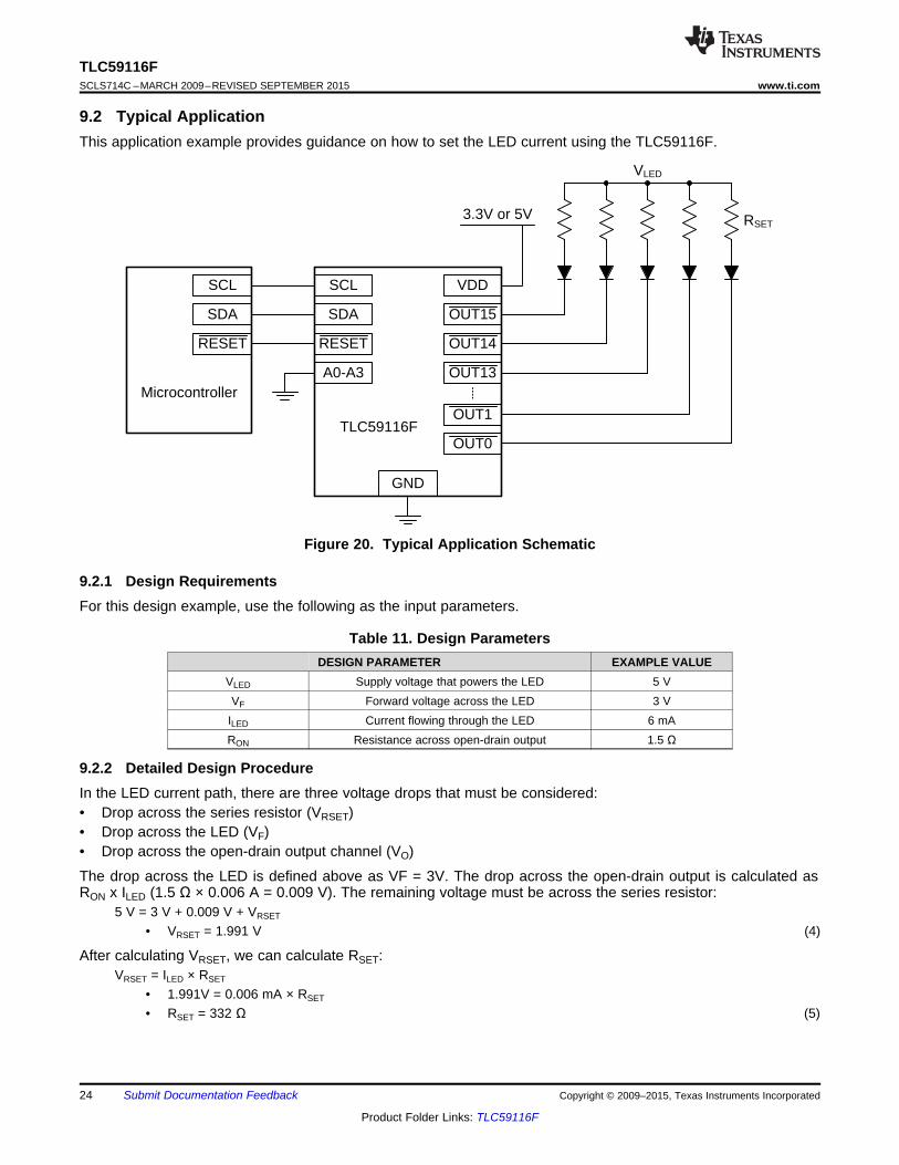
9.2 Typical ApplicationThis application example provides guidance on how to set the LED current using the TLC59116F.
Figure 20. Typical Application Schematic
9.2.1 Design RequirementsFor this design example, use the following as the input parameters.
Table 11. Design ParametersDESIGN PARAMETER EXAMPLE VALUE
VLED Supply voltage that powers the LED 5 VVF Forward voltage across the LED 3 V
ILED Current flowing through the LED 6 mARON Resistance across open-drain output 1.5 Ω
9.2.2 Detailed Design ProcedureIn the LED current path, there are three voltage drops that must be considered:• Drop across the series resistor (VRSET)• Drop across the LED (VF)• Drop across the open-drain output channel (VO)
The drop across the LED is defined above as VF = 3V. The drop across the open-drain output is calculated asRON x ILED (1.5 Ω × 0.006 A = 0.009 V). The remaining voltage must be across the series resistor:
5 V = 3 V + 0.009 V + VRSET
• VRSET = 1.991 V (4)
After calculating VRSET, we can calculate RSET:VRSET = ILED × RSET
• 1.991V = 0.006 mA × RSET
• RSET = 332 Ω (5)
24 Submit Documentation Feedback Copyright © 2009–2015, Texas Instruments Incorporated
Product Folder Links: TLC59116F

0
10
20
30
40
50
60
70
0 100 200 300 400 500 600 700
LED
Cur
rent
(m
A)
RSET (
VF = 2 V
VF = 3 V
VF = 4 V
C002
TLC59116Fwww.ti.com SCLS714C –MARCH 2009–REVISED SEPTEMBER 2015
9.2.3 Application Curve
VLED = 5 V
Figure 21. Typical LED Current as a Function of RSET and VF
Copyright © 2009–2015, Texas Instruments Incorporated Submit Documentation Feedback 25
Product Folder Links: TLC59116F

NC
A0
A1
A2
A3
OUT0
OUT1
OUT2
OUT3
GND
OUT4
OUT5
OUT6
OUT7
Vcc
SDA
SCL
RESET
GND
OUT15
OUT14
OUT13
OUT12
GND
OUT11
OUT10
OUT9
OUT8
VIA to GND
To µC
To µC
To µC
TLC59116FSCLS714C –MARCH 2009–REVISED SEPTEMBER 2015 www.ti.com
10 Power Supply RecommendationsTLC59116F is designed to operate from a VCC range of 3 V to 5.5 V. The system will also require a powersupply for the LEDs. The supply voltage for the LEDs must be greater than the forward voltage of the LED plusthe VOL of the channel.
11 Layout
11.1 Layout GuidelinesThe I2C signals (SDA / SCL) should be kept away from potential noise sources.
The traces carrying power through the LEDS should be wide enough to the handle necessary current.
All LED current passes through the device and into the ground node. There must be a strong connectionbetween the device ground and the circuit board ground. For the RHB package, the thermal pad should beconnected to ground to help dissipate heat.
11.2 Layout Examples
Figure 22. PW Layout Example
26 Submit Documentation Feedback Copyright © 2009–2015, Texas Instruments Incorporated
Product Folder Links: TLC59116F

A0
A1
A2A3
OUT0OUT1OUT2OUT3GND
OUT4
OU
T5
OU
T6
OU
T7
VC
CS
DA
SC
L
RESETGNDOUT15OUT14OUT13OUT12GNDOUT11
OU
T10
OU
T9
OU
T8
NC
NC
NC
NC
VIA to GND
To µC
To µC
To µC
NC
TLC59116Fwww.ti.com SCLS714C –MARCH 2009–REVISED SEPTEMBER 2015
Layout Examples (continued)
Figure 23. RHB Layout Example
Copyright © 2009–2015, Texas Instruments Incorporated Submit Documentation Feedback 27
Product Folder Links: TLC59116F

TLC59116FSCLS714C –MARCH 2009–REVISED SEPTEMBER 2015 www.ti.com
12 Device and Documentation Support
12.1 Community ResourcesThe following links connect to TI community resources. Linked contents are provided "AS IS" by the respectivecontributors. They do not constitute TI specifications and do not necessarily reflect TI's views; see TI's Terms ofUse.
TI E2E™ Online Community TI's Engineer-to-Engineer (E2E) Community. Created to foster collaborationamong engineers. At e2e.ti.com, you can ask questions, share knowledge, explore ideas and helpsolve problems with fellow engineers.
Design Support TI's Design Support Quickly find helpful E2E forums along with design support tools andcontact information for technical support.
12.2 TrademarksE2E is a trademark of Texas Instruments.All other trademarks are the property of their respective owners.
12.3 Electrostatic Discharge CautionThese devices have limited built-in ESD protection. The leads should be shorted together or the device placed in conductive foamduring storage or handling to prevent electrostatic damage to the MOS gates.
12.4 GlossarySLYZ022 — TI Glossary.
This glossary lists and explains terms, acronyms, and definitions.
13 Mechanical, Packaging, and Orderable InformationThe following pages include mechanical, packaging, and orderable information. This information is the mostcurrent data available for the designated devices. This data is subject to change without notice and revision ofthis document. For browser-based versions of this data sheet, refer to the left-hand navigation.
28 Submit Documentation Feedback Copyright © 2009–2015, Texas Instruments Incorporated
Product Folder Links: TLC59116F

PACKAGE OPTION ADDENDUM
www.ti.com 25-Feb-2015
Addendum-Page 1
PACKAGING INFORMATION
Orderable Device Status(1)
Package Type PackageDrawing
Pins PackageQty
Eco Plan(2)
Lead/Ball Finish(6)
MSL Peak Temp(3)
Op Temp (°C) Device Marking(4/5)
Samples
TLC59116FIPWR ACTIVE TSSOP PW 28 2000 Green (RoHS& no Sb/Br)
CU NIPDAU Level-1-260C-UNLIM -40 to 85 Y59116F
TLC59116FIRHBR ACTIVE VQFN RHB 32 3000 Green (RoHS& no Sb/Br)
CU NIPDAU Level-2-260C-1 YEAR -40 to 85 FL116F
(1) The marketing status values are defined as follows:ACTIVE: Product device recommended for new designs.LIFEBUY: TI has announced that the device will be discontinued, and a lifetime-buy period is in effect.NRND: Not recommended for new designs. Device is in production to support existing customers, but TI does not recommend using this part in a new design.PREVIEW: Device has been announced but is not in production. Samples may or may not be available.OBSOLETE: TI has discontinued the production of the device.
(2) Eco Plan - The planned eco-friendly classification: Pb-Free (RoHS), Pb-Free (RoHS Exempt), or Green (RoHS & no Sb/Br) - please check http://www.ti.com/productcontent for the latest availabilityinformation and additional product content details.TBD: The Pb-Free/Green conversion plan has not been defined.Pb-Free (RoHS): TI's terms "Lead-Free" or "Pb-Free" mean semiconductor products that are compatible with the current RoHS requirements for all 6 substances, including the requirement thatlead not exceed 0.1% by weight in homogeneous materials. Where designed to be soldered at high temperatures, TI Pb-Free products are suitable for use in specified lead-free processes.Pb-Free (RoHS Exempt): This component has a RoHS exemption for either 1) lead-based flip-chip solder bumps used between the die and package, or 2) lead-based die adhesive used betweenthe die and leadframe. The component is otherwise considered Pb-Free (RoHS compatible) as defined above.Green (RoHS & no Sb/Br): TI defines "Green" to mean Pb-Free (RoHS compatible), and free of Bromine (Br) and Antimony (Sb) based flame retardants (Br or Sb do not exceed 0.1% by weightin homogeneous material)
(3) MSL, Peak Temp. - The Moisture Sensitivity Level rating according to the JEDEC industry standard classifications, and peak solder temperature.
(4) There may be additional marking, which relates to the logo, the lot trace code information, or the environmental category on the device.
(5) Multiple Device Markings will be inside parentheses. Only one Device Marking contained in parentheses and separated by a "~" will appear on a device. If a line is indented then it is a continuationof the previous line and the two combined represent the entire Device Marking for that device.
(6) Lead/Ball Finish - Orderable Devices may have multiple material finish options. Finish options are separated by a vertical ruled line. Lead/Ball Finish values may wrap to two lines if the finishvalue exceeds the maximum column width.
Important Information and Disclaimer:The information provided on this page represents TI's knowledge and belief as of the date that it is provided. TI bases its knowledge and belief on informationprovided by third parties, and makes no representation or warranty as to the accuracy of such information. Efforts are underway to better integrate information from third parties. TI has taken andcontinues to take reasonable steps to provide representative and accurate information but may not have conducted destructive testing or chemical analysis on incoming materials and chemicals.TI and TI suppliers consider certain information to be proprietary, and thus CAS numbers and other limited information may not be available for release.

PACKAGE OPTION ADDENDUM
www.ti.com 25-Feb-2015
Addendum-Page 2
In no event shall TI's liability arising out of such information exceed the total purchase price of the TI part(s) at issue in this document sold by TI to Customer on an annual basis.

TAPE AND REEL INFORMATION
*All dimensions are nominal
Device PackageType
PackageDrawing
Pins SPQ ReelDiameter
(mm)
ReelWidth
W1 (mm)
A0(mm)
B0(mm)
K0(mm)
P1(mm)
W(mm)
Pin1Quadrant
TLC59116FIPWR TSSOP PW 28 2000 330.0 16.4 6.9 10.2 1.8 12.0 16.0 Q1
TLC59116FIRHBR VQFN RHB 32 3000 330.0 12.4 5.3 5.3 1.5 8.0 12.0 Q2
PACKAGE MATERIALS INFORMATION
www.ti.com 22-Feb-2016
Pack Materials-Page 1

*All dimensions are nominal
Device Package Type Package Drawing Pins SPQ Length (mm) Width (mm) Height (mm)
TLC59116FIPWR TSSOP PW 28 2000 367.0 367.0 38.0
TLC59116FIRHBR VQFN RHB 32 3000 367.0 367.0 35.0
PACKAGE MATERIALS INFORMATION
www.ti.com 22-Feb-2016
Pack Materials-Page 2


IMPORTANT NOTICE
Texas Instruments Incorporated and its subsidiaries (TI) reserve the right to make corrections, enhancements, improvements and otherchanges to its semiconductor products and services per JESD46, latest issue, and to discontinue any product or service per JESD48, latestissue. Buyers should obtain the latest relevant information before placing orders and should verify that such information is current andcomplete. All semiconductor products (also referred to herein as “components”) are sold subject to TI’s terms and conditions of salesupplied at the time of order acknowledgment.TI warrants performance of its components to the specifications applicable at the time of sale, in accordance with the warranty in TI’s termsand conditions of sale of semiconductor products. Testing and other quality control techniques are used to the extent TI deems necessaryto support this warranty. Except where mandated by applicable law, testing of all parameters of each component is not necessarilyperformed.TI assumes no liability for applications assistance or the design of Buyers’ products. Buyers are responsible for their products andapplications using TI components. To minimize the risks associated with Buyers’ products and applications, Buyers should provideadequate design and operating safeguards.TI does not warrant or represent that any license, either express or implied, is granted under any patent right, copyright, mask work right, orother intellectual property right relating to any combination, machine, or process in which TI components or services are used. Informationpublished by TI regarding third-party products or services does not constitute a license to use such products or services or a warranty orendorsement thereof. Use of such information may require a license from a third party under the patents or other intellectual property of thethird party, or a license from TI under the patents or other intellectual property of TI.Reproduction of significant portions of TI information in TI data books or data sheets is permissible only if reproduction is without alterationand is accompanied by all associated warranties, conditions, limitations, and notices. TI is not responsible or liable for such altereddocumentation. Information of third parties may be subject to additional restrictions.Resale of TI components or services with statements different from or beyond the parameters stated by TI for that component or servicevoids all express and any implied warranties for the associated TI component or service and is an unfair and deceptive business practice.TI is not responsible or liable for any such statements.Buyer acknowledges and agrees that it is solely responsible for compliance with all legal, regulatory and safety-related requirementsconcerning its products, and any use of TI components in its applications, notwithstanding any applications-related information or supportthat may be provided by TI. Buyer represents and agrees that it has all the necessary expertise to create and implement safeguards whichanticipate dangerous consequences of failures, monitor failures and their consequences, lessen the likelihood of failures that might causeharm and take appropriate remedial actions. Buyer will fully indemnify TI and its representatives against any damages arising out of the useof any TI components in safety-critical applications.In some cases, TI components may be promoted specifically to facilitate safety-related applications. With such components, TI’s goal is tohelp enable customers to design and create their own end-product solutions that meet applicable functional safety standards andrequirements. Nonetheless, such components are subject to these terms.No TI components are authorized for use in FDA Class III (or similar life-critical medical equipment) unless authorized officers of the partieshave executed a special agreement specifically governing such use.Only those TI components which TI has specifically designated as military grade or “enhanced plastic” are designed and intended for use inmilitary/aerospace applications or environments. Buyer acknowledges and agrees that any military or aerospace use of TI componentswhich have not been so designated is solely at the Buyer's risk, and that Buyer is solely responsible for compliance with all legal andregulatory requirements in connection with such use.TI has specifically designated certain components as meeting ISO/TS16949 requirements, mainly for automotive use. In any case of use ofnon-designated products, TI will not be responsible for any failure to meet ISO/TS16949.
Products ApplicationsAudio www.ti.com/audio Automotive and Transportation www.ti.com/automotiveAmplifiers amplifier.ti.com Communications and Telecom www.ti.com/communicationsData Converters dataconverter.ti.com Computers and Peripherals www.ti.com/computersDLP® Products www.dlp.com Consumer Electronics www.ti.com/consumer-appsDSP dsp.ti.com Energy and Lighting www.ti.com/energyClocks and Timers www.ti.com/clocks Industrial www.ti.com/industrialInterface interface.ti.com Medical www.ti.com/medicalLogic logic.ti.com Security www.ti.com/securityPower Mgmt power.ti.com Space, Avionics and Defense www.ti.com/space-avionics-defenseMicrocontrollers microcontroller.ti.com Video and Imaging www.ti.com/videoRFID www.ti-rfid.comOMAP Applications Processors www.ti.com/omap TI E2E Community e2e.ti.comWireless Connectivity www.ti.com/wirelessconnectivity
Mailing Address: Texas Instruments, Post Office Box 655303, Dallas, Texas 75265Copyright © 2016, Texas Instruments Incorporated