Embed Size (px)
Citation preview
Title Two-dimensional network of atomtronic qubits Author(s) S. Safaei, B. Grémaud, R. Dumke, L.-C. Kwek, L. Amico and C. Miniatura Source Physical Review A, 97, 042306 Published by American Physical Society Copyright © 2018 American Physical Society
This document may be used for private study or research purpose only. This document or any part of it may not be duplicated and/or distributed without permission of the copyright owner. The Singapore Copyright Act applies to the use of this document. Citation: Safaei, S., Grémaud, B., Dumke, R., Kwek, L. C., Amico, L., & Miniatura, C. (2018). Two-dimensional network of atomtronic qubits. Physical Review A, 97, 042306. http://dx.doi.org/10.1103/PhysRevA.97.042306 This document was archived with permission from the copyright owner.
Two-dimensional network of atomtronic qubits
S. Safaei,1, 2 B. Grémaud,2, 1, 3, 4 R. Dumke,1, 5, 2 L.-C. Kwek,1, 6, 7, 2 L. Amico,8, 9, 1 and C. Miniatura2, 1, 3, 5, 10, 7
1Centre for Quantum Technologies, National University of Singapore, 3 Science Drive 2, 117543 Singapore2MajuLab, CNRS-UCA-SU-NUS-NTU International Joint Research Unit, Singapore
3Physics Department, Faculty of Science, National University of Singapore, 2 Science Drive 3, 117551 Singapore4Laboratoire Kastler Brossel, Ecole Normale Supérieure CNRS, UPMC; 4 Place Jussieu 75005 Paris, France
5Division of Physics and Applied Physics, School of Physical and Mathematical Sciences,Nanyang Technological University, 21 Nanyang Link, Singapore 637371
6National Institute of Education and Institute of Advanced Studies,Nanyang Technological University, 1 Nanyang Walk, Singapore 637616
7Institute of Advanced Studies, Nanyang Technological University, 60 Nanyang View, Singapore 639673, Singapore8INFN-Laboratori Nazionali del Sud, INFN, via S. Soa 62, 95123 Catania, Italy.
9CNR-MATIS-IMM & Dipartimento di Fisica e Astronomia, Via S. Soa 64, 95127 Catania, Italy10Université Côte d'Azur, CNRS, INPHYNI; France
Through a combination of laser beams, we engineer a 2D optical lattice of Mexican hat potentialsable to host atoms in its ring-shaped wells. When tunneling can be ignored (at high laser intensities),we show that a well-dened qubit can be associated with the states of the atoms trapped in each ofthe rings. Each of these two-level systems can be manipulated by a suitable conguration of Ramanlaser beams imprinting a synthetic ux onto each Mexican hat cell of the lattice. Overall, we believethat the system has the potential to form a scalable architecture for atomtronic ux qubits.
PACS numbers: 03.67.Lx, 37.10.Jk
I. INTRODUCTION
Atomtronics aims at exploiting the matter wave as-pects of quantum cold-atom systems conned in magneticor laser light circuits of complex shapes [13]. Several el-ementary atomtronic devices and circuits have alreadybeen proposed [47] and some have been realized [812]. The construction of atomtronic integrated circuits,though, remains an important open problem not only inquantum optics but in the broader eld of quantum tech-nology. In this paper, we propose a scheme to create anetwork of atomtronic rings with the potential to be usedas ux qubits for information processing. Crucially, theapproach might prove scalable.
Qubits can be implemented in a variety of physicalsystems [1318] with dierent advantages and disadvan-tages. Solid-state realizations allow the construction offast gates (nanoseconds) but need to operate at shorttime scales (microseconds) to ght decoherence and/ordissipation. An important advantage of such congura-tions is that they benet from the scalability provided byhighly-developed lithographic techniques. On the otherhand, atomic qubits realized by hyperne states of coldatoms conned in optical lattices have very long storageand coherence times (fraction of a second). For such sys-tems, scalability has been achieved in principle [19], butsingle-site addressability is the main bottleneck in quan-tum processing with cold atoms.
With atomtronic ux qubits, we seek to combine themacroscopic quantum coherence of the Josephson junc-tion ux qubits with the advantages of cold atoms [2022]. The devices have the phenomenology of an atom-tronic quantum interference device (AQUID), the atomiccounterpart of a superconducting quantum interference
device (SQUID), and they operate with a ring-shapedBose-Einstein condensate (BEC). The two-level systemis based on clockwise and anti-clockwise atomic currentsobtained by applying an eective gauge eld to the sys-tem [23]. In the simplest scheme, superpositions of thesecurrent states are generated by forward and back scatter-ing ows of the cold atoms through a single tunnel barrier(weak link) that is imprinted along the ring-shaped po-tential (breaking the Galilean invariance of the system).Although schemes for single or few coupled atomtronicqubits have been conceived [21, 24], the implementationsare complex. As a consequence, it is challenging to takea "bottom-up" approach to a scalable architecture. In-stead, in this paper, we pursue a "top-down" approach.
We propose a laser scheme to realize a pattern of closedcircular currents arranged in a planar conguration. Sucha pattern emerges from a two-dimensional (2D) opticallattice consisting of a triangular periodic array of Mex-ican hat potentials. Atoms can be trapped in its nearly
ring-shaped conning wells. The scheme is completed byapplying a suitable laser conguration subjecting the lat-tice to an eective gauge eld. We demonstrate that aneective two-level system arises in each elementary cellof the 2D lattice. Furthermore, the system can be con-trolled by the eective gauge eld. Overall, our systemwould potentially constitute a 2D architecture hostingux qubits. We mention possible schemes to address,couple, and manipulate the two-level systems arrangedin such a 2D Mexican hat lattice.
The rest of the paper is organized as follows. In Sec. IIwe explain the laser conguration used to produce thelattice of Mexican hat potentials. In Sec. III we discussthe condition under which the Mexican hats (rings) arepractically decoupled. Next, in Sec. IV, we show how
2
dierent parameters of the system can be tuned in orderto engineer the energy spectrum of each single Mexicanhat and obtain a spectrum similar to the one of super-conducting ux qubits. We discuss the feasibility of thesystem, referring to typical required experimental param-eters, in Sec. V and briey mention how qubit gates couldbe implemented in Sec.VI. We summarize our work andconclude with some perspectives in Sec. VII.
II. 2D MEXICAN HAT LATTICE LASER
CONFIGURATION
We consider atoms (mass m, resonance frequency ωat,linewidth Γ) subjected to three coplanar standing waveslying in the xy-plane at relative angles π/3 to each other.They are produced by three retro-reected monochro-matic laser beams (same frequency ωL) linearly-polarizedalong axis Oz. The corresponding wave vectors are~k1 = kL
(√32 x + 1
2 y), ~k2 = kL
(−√32 x + 1
2 y), and
~k3 = ~k1 + ~k2 = kLy, with kL = ωL/c = 2π/λL (λL is thelaser wavelength), and we assume their respective Rabifrequencies to be Ω1 = Ω2 = γΩ and Ω3 = Ω. The exter-nally adjustable parameter γ is the relative strength ofthe two lateral standing waves compared to the one alongOy. For far blue-detuned laser beams (positive detuningδL = ωL − ωat Γ), and after a suitable choice of theorigin of coordinates, the light-shift potential experiencedby the atoms is V (~r) = U0v(~r) where:
v(~r) =[
cos kLy + 2γ cos(kLy + φ
2) cos(
√3kLx
2)]2
(1)
and U0 = ~Ω2/(4δL) > 0. Note that xing the originimposes two conditions on the phases of the lasers, thusleaving only one adjustable phase parameter, φ, in theequation above. The full optical potential shows up asa triangular lattice of Mexican hat structures, with theunit Bravais cell being spanned by ~a1 = λL( 1√
3x+ y) and
~a2 = λL(− 1√3x+ y) [25].
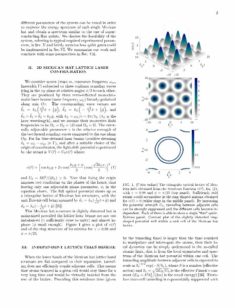
This Mexican hat structure is slightly distorted but ismaintained provided the lattice laser beams are not tooimbalanced (γ suciently close to unity) and almost in-phase (φ small enough). Figure 1 gives a plot of v(~r)and of the ring structure of its minima for γ = 0.98 andφ = π/25.
III. INDEPENDENT LATTICE CELLS REGIME
When the lower bands of the Mexican hat lattice bandstructure are at compared to their separation, tunnel-ing does not eciently couple adjacent cells. This meansthat atoms trapped in a given cell would stay there for avery long time and would be virtually isolated from therest of the lattice. Providing this residence time (given
FIG. 1. (Color online) The triangular optical lattice of Mex-ican hats obtained from the structure function v(~r), Eq. (1),with γ = 0.98 and φ = π/25 (top panel). Suciently coldatoms would accumulate in the ring-shaped minima obtainedfor v(~r) = 0 (white rings in the middle panel). By increasingthe potential strength U0, tunneling between adjacent cellscan be strongly suppressed and the dierent cells become in-dependent. Each of them is able to store a single "ux" qubit.Bottom panel: Contour plot of the slightly distorted ring-shaped potential well within a unit cell of the Mexican hatlattice.
by the tunneling time) is larger than the time requiredto manipulate and interrogate the atoms, then their lo-cal dynamics can be simply understood in the so-calledatomic limit, that is from the local eigenstates and spec-trum of the Mexican hat potential within one cell. Thetunneling amplitude between adjacent cells is expected to
scale as ~−3/2e exp(−S/~e), where S is a number (eective
action) and ~e =√
2ER/U0 is the eective Planck's con-stant (ER = ~2k2L/(2m) is the recoil energy) [26]. There-fore inter-cell tunneling is exponentially suppressed with
3
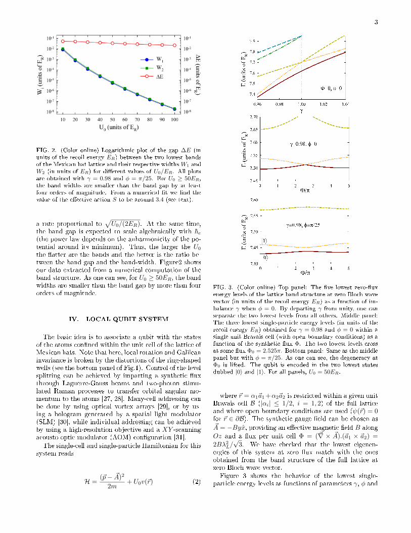
FIG. 2. (Color online) Logarithmic plot of the gap ∆E (inunits of the recoil energy ER) between the two lowest bandsof the Mexican hat lattice and their respective widthsW1 andW2 (in units of ER) for dierent values of U0/ER. All plotsare obtained with γ = 0.98 and φ = π/25. For U0 ≥ 50ER,the band widths are smaller than the band gap by at leastfour orders of magnitude. From a numerical t we nd thevalue of the eective action S to be around 3.4 (see text).
a rate proportional to√U0/(2ER). At the same time,
the band gap is expected to scale algebraically with ~e(the power law depends on the anharmonicity of the po-tential around its minimum). Thus, the larger the U0
the atter are the bands and the better is the ratio be-tween the band gap and the band-width. Figure2 showsour data extracted from a numerical computation of theband structure. As one can see, for U0 ≥ 50ER, the bandwidths are smaller than the band gap by more than fourorders of magnitude.
IV. LOCAL QUBIT SYSTEM
The basic idea is to associate a qubit with the statesof the atoms conned within the unit cell of the lattice ofMexican hats. Note that here, local rotation and Galileaninvariance is broken by the distortions of the ring-shapedwells (see the bottom panel of Fig.1). Control of the levelsplitting can be achieved by imparting a synthetic uxthrough Laguerre-Gauss beams and two-photon stimu-lated Raman processes to transfer orbital angular mo-mentum to the atoms [27, 28]. Many-cell addressing canbe done by using optical vortex arrays [29], or by us-ing a hologram generated by a spatial light modulator(SLM) [30], while individual addressing can be achievedby using a high-resolution objective and a XY -scanningacousto-optic modulator (AOM) conguration [31].
The single-cell and single-particle Hamiltonian for thissystem reads
H =(~p− ~A)2
2m+ U0v(~r) (2)
FIG. 3. (Color online) Top panel: The ve lowest zero-uxenergy levels of the lattice band structure at zero Bloch wavevector (in units of the recoil energy ER) as a function of im-balance γ when φ = 0. By departing γ from unity, one canseparate the two lowest levels from all others. Middle panel:The three lowest single-particle energy levels (in units of therecoil energy ER) obtained for γ = 0.98 and φ = 0 within asingle unit Bravais cell (with open boundary conditions) as afunction of the synthetic ux Φ. The two lowest levels crossat some ux Φ0 = 2.525π. Bottom panel: Same as the middlepanel but with φ = π/25. As one can see, the degeneracy atΦ0 is lifted. The qubit is encoded in the two lowest statesdubbed |0〉 and |1〉. For all panels, U0 = 50ER.
where ~r = α1~a1 +α2~a2 is restricted within a given unitBravais cell B (|αi| ≤ 1/2, i = 1, 2) of the full latticeand where open boundary conditions are used (ψ(~r) = 0for ~r ∈ ∂B). The synthetic gauge eld can be chosen as~A = −Byx, providing an eective magnetic eld B along
Oz and a ux per unit cell Φ = (~∇ × ~A).(~a1 × ~a2) =
2Bλ2L/√
3. We have checked that the lowest eigenen-ergies of this system at zero ux match with the onesobtained from the band structure of the full lattice atzero Bloch wave vector.Figure 3 shows the behavior of the lowest single-
particle energy levels as functions of parameters γ, φ and
4
ux Φ. Starting from the lattice band structure obtainedat zero Bloch wave vector, we isolate two levels from allothers by departing γ from unity (top panel). Choos-ing γ = 0.98, we next compute how these levels changewith the ux Φ generated by an articial gauge eld im-printed on the atoms (middle panel). The two lowestlevels cross at some ux Φ0 ≈ 2.525π. A small phasedierence φ = π/25 then serves to lift the degeneracy atΦ0, the third level being still suciently away (bottompanel). For this set of parameters, we thus get the typi-cal level behavior of ux qubits with an avoided crossing.We use the corresponding states, dubbed |0〉 and |1〉, toencode a qubit in each of the unit cells of the lattice ofMexican hats.
V. FEASIBILITY
Considering, as an example, 87Rb atoms and the S1/2 -P3/2 transition (ωat = 2π×384.23 THz, λat = 780.24 nm,Γ = 2π × 6.06 MHz), one could use blue-detuned lasersby δL = 2π× 6 THz (or, equivalently, λat−λL = 12 nm)to produce the lattice. In this case, a lattice with overallstrength U0 = 100ER requires laser intensities I = 4.1MW/m2. Therefore, lasers with a power of 1W would beable to produce a lattice area of 500µm × 500µm whichwould host more than 250000 unit-cells/qubits. Stabiliz-ing the lattice strength U0 at a level of 4% is achievedby stabilizing the laser output power at the same level(or at 20% in Rabi frequency), which is feasible. Thelattice structure is determined by the values chosen forφ and γ. Taking φ = 0 as the reference point, settingφ = π/25 = 0.02 × 2π requires moving the mirror alongOy by 0.02 λL = 15.4 nm. This is within the range ofthe current technology which allows precise and stablenanometer positioning [35, 36]. Fixing γ = 0.98 requiresxing the ratio of the Rabi frequencies with a precisionbetter than 2%.
VI. COMMENTS ON QUANTUM GATES AND
READ-OUT
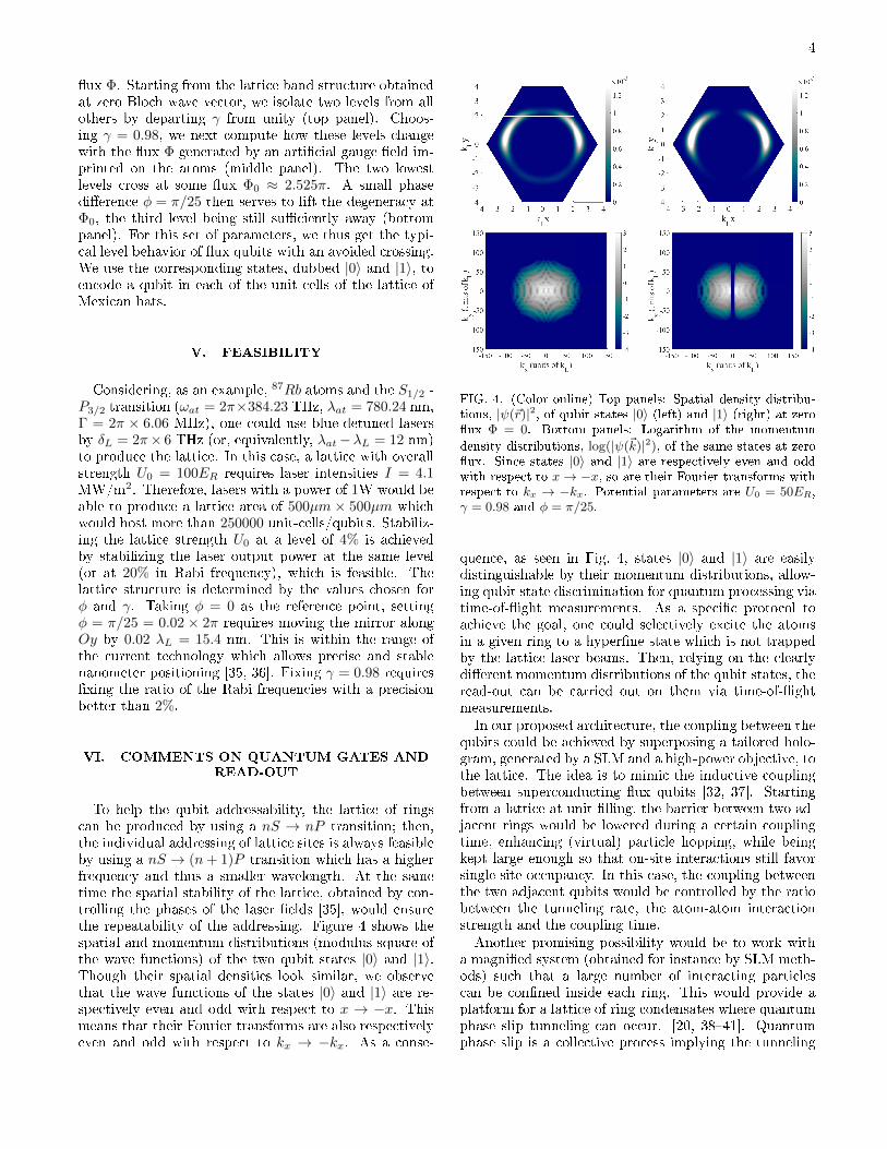
To help the qubit addressability, the lattice of ringscan be produced by using a nS → nP transition; then,the individual addressing of lattice sites is always feasibleby using a nS → (n+ 1)P transition which has a higherfrequency and thus a smaller wavelength. At the sametime the spatial stability of the lattice, obtained by con-trolling the phases of the laser elds [35], would ensurethe repeatability of the addressing. Figure 4 shows thespatial and momentum distributions (modulus square ofthe wave functions) of the two qubit states |0〉 and |1〉.Though their spatial densities look similar, we observethat the wave functions of the states |0〉 and |1〉 are re-spectively even and odd with respect to x → −x. Thismeans that their Fourier transforms are also respectivelyeven and odd with respect to kx → −kx. As a conse-
FIG. 4. (Color online) Top panels: Spatial density distribu-tions, |ψ(~r)|2, of qubit states |0〉 (left) and |1〉 (right) at zeroux Φ = 0. Bottom panels: Logarithm of the momentumdensity distributions, log(|ψ(~k)|2), of the same states at zeroux. Since states |0〉 and |1〉 are respectively even and oddwith respect to x→ −x, so are their Fourier transforms withrespect to kx → −kx. Potential parameters are U0 = 50ER,γ = 0.98 and φ = π/25.
quence, as seen in Fig. 4, states |0〉 and |1〉 are easilydistinguishable by their momentum distributions, allow-ing qubit state discrimination for quantum processing viatime-of-ight measurements. As a specic protocol toachieve the goal, one could selectively excite the atomsin a given ring to a hyperne state which is not trappedby the lattice laser beams. Then, relying on the clearlydierent momentum distributions of the qubit states, theread-out can be carried out on them via time-of-ightmeasurements.In our proposed architecture, the coupling between the
qubits could be achieved by superposing a tailored holo-gram, generated by a SLM and a high-power objective, tothe lattice. The idea is to mimic the inductive couplingbetween superconducting ux qubits [32, 37]. Startingfrom a lattice at unit lling, the barrier between two ad-jacent rings would be lowered during a certain couplingtime, enhancing (virtual) particle hopping, while beingkept large enough so that on-site interactions still favorsingle site occupancy. In this case, the coupling betweenthe two adjacent qubits would be controlled by the ratiobetween the tunneling rate, the atom-atom interactionstrength and the coupling time.Another promising possibility would be to work with
a magnied system (obtained for instance by SLM meth-ods) such that a large number of interacting particlescan be conned inside each ring. This would provide aplatform for a lattice of ring condensates where quantumphase slip tunneling can occur. [20, 3841]. Quantumphase slip is a collective process implying the tunneling

5
of the phase degree of freedom of the cold atoms owinginto adjacent qubits of the lattice. Such processes occurclose to the Mott insulating states in which phase uc-tuations are suciently strong to trigger the tunnelingof the phase states [42]. Because of such tunneling, eachpersistent current will be coupled to the other persis-tent current owing in the other qubit. Referring to thesuperconducting platform, the experiments conducted oncircuits involving uxonium architectures evidence quan-tum phase slip tunneling rates of the order of 1−10 GHz[40, 43]. With cold atoms however, there has been no ex-periment so far. Clearly, the time scales are very dierent(milliseconds) and therefore quantum phase slips in ourcold atom system may be expected in the kHz range.A description of protocols based on quantum phase slipand analysis of their performances would require a de-tailed study on its own and is beyond the scope of thispaper.Regardless of the actual coupling scenario, eective
coupling terms of the form σz ⊗ σz and σx ⊗ σx be-tween adjacent qubits are expected. Then one couldenvisage implementing a two-qubit controlled-NOT gateanalogously to superconducting ux qubits. It is alsoworth mentioning that the main source of decoherence inour system is expected to come from collisions with thebackground gas, leading to decoherence time scales of theorder of tens of seconds. Together with single gate oper-ations, such a system of ring condensates, arranged in atriangular lattice, would have the potential to generatea two-qubit universal quantum gate [3234]. With thisapproach one could even couple many dierent pairs ofadjacent qubits in parallel. Here again, the spatial sta-bility of the lattice potential is essential for a successfulimplementation of the scheme.
VII. CONCLUSION
We have proposed a laser scheme providing a possiblescalable architecture of ring qubits placed in the elemen-
tary cells of a triangular lattice and realizing an atom-tronic light circuit. Each qubit is rendered by a quantumparticle moving in the (distorted) ring-shaped minimumof a Mexican hat potential. The typical spatial extensionof each qubit is of a few microns but could be magnied tolarger sizes by SLM techniques. The obtained triangular2D array of atomtronic ring qubits can be manipulatedsimilarly to superconducting ux qubits, but with an ef-fective magnetic eld generated by Laguerre-Gauss laserbeams imprinting a synthetic gauge eld on the atoms.The ux state can be determined by interference mea-surements [10] or by Doppler measurement of the quan-tized ow state [44]. Future studies should consider therole of atom-atom interactions and address the couplingbetween the condensates wavefunctions within adjacentring-shaped potential minima [45] as well as the perfor-mances of such a system for quantum information pro-cessing purposes. Finally, we observe that, beyond quan-tum information purposes, our scheme could be viewedas a quantum simulator made of ultracold atoms vortexarrays [4648] or as a quantum sensor based on light-matter angular momentum transfer [49].
VIII. ACKNOWLEDGEMENTS
This research is supported by the National ResearchFoundation, Prime Minister's Oce, Singapore and theMinistry of Education-Singapore under the ResearchCentres of Excellence programme and Academic Re-search Fund Tier 2 (Grant No. MOE2015-T2-1-101).
[1] B. T. Seaman, M. Krämer, D. Z. Anderson, and M. J.Holland, Phys. Rev. A 75, 023615 (2007).
[2] L. Amico, and M. G. Boshier, J. Opt. 18 093001 (2016);[3] L. Amico, G. Birkl, M. G. Boshier, and L.-C. Kwek, New
J. Phys. 19 020201 (2017).[4] A. Micheli, A. J. Daley, D. Jaksch, and P. Zoller, Phys.
Rev. Lett. 93, 140408 (2004).[5] J. A. Stickney, D. Z. Anderson, and A. A. Zozulya, Phys.
Rev. A 75, 013608 (2007).[6] R. A. Pepino, J. Cooper, D. Z. Anderson, and M. J.
Holland, Phys. Rev. Lett. 103, 140405 (2009).[7] R. A. Pepino, J. Cooper, D. Meiser, D. Z. Anderson, and
M. J. Holland, Phys. Rev. A 82, 013640 (2010).[8] S. C. Caliga, C. J. E. Straatsma, A. A. Zozulya, and D.
Z. Anderson, New J. Phys. 18, 015012 (2016).
[9] A. Ramanathan, K. C. Wright, S. R. Muniz, M. Zelan,W. T. Hill, C. J. Lobb, K. Helmerson, W. D. Phillips, andG. K. Campbell, Phys. Rev. Lett. 106, 130401 (2011).
[10] S. Eckel, F. Jendrzejewski, A. Kumar, C. J. Lobb, andG. K. Campbell, Phys. Rev. X 4, 031052 (2014).
[11] C. Ryu, M. F. Andersen, P. Cladé, V. Natarajan, K.Helmerson, and W. D. Phillips, Phys. Rev. Lett. 99,260401 (2007).
[12] C. Ryu and M. G. Boshier, New J. Phys. 17, 092002(2015).
[13] J. Clarke and F. K. Wilhelm, Nature (London) 453, 1031(2008).
[14] I. Bloch, Nature (London) 453, 1016 (2008).[15] M. Saman, T. Walker, and K. Mølmer, Rev. Mod.
Phys. 82, 2313 (2010).

6
[16] R. Blatt, and D. Wineland, Nature (London) 453, 1008(2008).
[17] L. M. Vandersypen, M. Steen, G. Breyta, C. S. Yan-noni, M. H. Sherwood, and I. L. Chuang, Nature (Lon-don) 414, 883 (2001).
[18] J. Petta, A. C. Johnson, J. Taylor, E. Laird, A. Yacoby,M. D. Lukin, C. Marcus, M. Hanson, and A Gossard,Science 309, 2180 (2005).
[19] The scalability is limited by the diraction limit of thelaser light conning potential, R. Dumke, M. Volk, T.Müther, F. B. J. Buchkremer, G. Birkl, and W. Ertmer,Phys. Rev. Lett. 89, 097903 (2002).
[20] D. Solenov and D. Mozyrsky, J. Comput. Theor.Nanosci. 8, 481 (2011).
[21] L. Amico, D. Aghamalyan, F. Auksztol, H. Crepaz, R.Dumke, and L.-C. Kwek, Sci. Rep. 4, 4298 (2014).
[22] D. Aghamalyan, N. Nguyen, F. Auksztol, K. Gan, M.M. Valado, P. Condylis, L.-C. Kwek, R. Dumke, and L.Amico, New J. Phys. 18, 075013 (2016).
[23] J. Dalibard, F. Gerbier, G. Juzeliunas, and P. Öhberg,Rev. Mod. Phys. 83, 1523 (2011).
[24] D. Aghamalyan, L. Amico, and L.-C. Kwek, Phys. Rev.A 88, 063627 (2013).
[25] S. Safaei, C. Miniatura, and B. Grémaud, Phys. Rev.A 92, 043810 (2015).
[26] K. L. Lee, B. Grémaud, R. Han, B.-G. Englert, and C.Miniatura, Phys. Rev. A 80, 043411 (2009).
[27] M. F. Andersen, C. Ryu, P. Cladé, V. Natarajan, A.Vaziri, K. Helmerson, and W. D. Phillips, Phys. Rev.Lett. 97, 170406 (2006).
[28] G. Nandi, R. Walser, and W. P. Schleich, Phys. Rev.A 69, 063606 (2004).
[29] Y. C. Lin, T. H. Lu, K. F. Huang, and Y. F. Chen, Opt.Express 19, 10293 (2011).
[30] G. Gauthier, I. Lenton, N. McKay Parry, M. Baker, M.J. Davis, H. Rubinsztain-Dunlop, and T. W. Neely, Op-tica 3, 1136 (2016).
[31] H. Labuhn, S. Ravets, D. Barredo, L. Béguin, F. No-grette, T. Lahaye, and A. Browaeys, Phys. Rev. A 90,023415 (2014).
[32] Y. Makhlin, G. Schön, and A. Shnirman, Rev. Mod.Phys. 73, 357 (2001).
[33] H. Fan, V. Roychowdhury, and T. Szkopek, Phys. Rev.A 72, 052323 (2005).
[34] D. Loss and D. P. DiVincenzo, Phys. Rev. A 57, 120(1998).
[35] C. T. Schmiegelow, H. Kaufmann, T. Ruster, J. Schulz,V. Kaushal, M. Hettrich, F. Schmidt-Kaler, and U. G.Poschinger, Phys. Rev. Lett. 116, 033002 (2016).
[36] T. J. Teo, V. P. Bui, G. Yang, and I.-M. Chen,EEE/ASME Transactions on Mechatronics 20, 2813(2015).
[37] J. Mooij, T. Orlando, L. Levitov, L. Tian, C. H. Van derWal, and S. Lloyd, Science 285, 1036 (1999).
[38] K. A. Matveev, A. I. Larkin, and L. I. Glazman, Phys.Rev. Lett. 89, 096802 (2002).
[39] G. Rastelli, I. M. Pop, F. W. J. Hekking, Phys. Rev.B 87, 174513 (2013).
[40] I. M. Pop, I. Protopopov, F. Lecocq, Z. Peng, B. Pan-netier, O. Buisson, and W.Guichard Nature Physics 6,589 (2010).
[41] O. V. Astaev, L. B. Ioe, S. Kafanov, Yu. A. Pashkin,K. Yu. Arutyunov, D. Shahar, O. Cohen, and J. S. TsaiNature (London) 484, 355 (2012).
[42] J. E. Mooij and U. Nazarov, Nat. Phys. 2, 169 (2006).[43] A. Kou, W. C. Smith, U. Vool, R. T. Brierley, H. Meier,
L. Frunzio, S. M. Girvin, L. I. Glazman, and M. H. De-voret, Phys. Rev. X 7, 031037 (2017).
[44] A. Kumar, N. Anderson, W. D. Phillips, S. Eckel, G.K. Campbell, and S. Stringari, New J. Phys. 18, 025001(2016).
[45] An eective description of the quantum dynamics interms of weak links could be envisaged for our system, asdone in Refs. [22, 37].
[46] Quantum Simulation-Nature Physics Insight, specialissue of, Nat. Phys. 8, 263 (2012), edited by A.Trabesinger.
[47] P. Vignolo, R. Fazio, and M. P. Tosi, Phys. Rev. A 76,023616 (2007).
[48] A. A. Burkov and E. Demler, Phys. Rev. Lett. 96, 180406(2006).
[49] L. Thiel, D. Rohner, M. Ganzhorn, P. Appel, E. Neu, B.Müller, R. Kleiner, D. Koelle, and P. Maletinsky, NatureNanotechnology 11, 677 (2016).
View publication statsView publication stats