Embed Size (px)
Citation preview

Title Development of ZnO and SnO2-Based Photoelectrodes forTandem Dye-Sensitized Solar Cells( 本文(Fulltext) )
Author(s) ASDIM
Report No.(DoctoralDegree) 博士(工学) 甲第454号
Issue Date 2014-03-25
Type 博士論文
Version ETD
URL http://hdl.handle.net/20.500.12099/49023
※この資料の著作権は、各資料の著者・学協会・出版社等に帰属します。

学位論文
Development of ZnO and SnO2–Based Photoelectrodes
for Tandem Dye-Sensitized Solar Cells
積層型色素増感太陽電池に用いる酸化亜鉛,
酸化スズ光電極の開発
平成 26年度 3月
岐阜大学大学院工学研究科
環境エネルギーシステム専攻
ASDIM
2
Contents
Chapter 1. General Introduction..................................................................................4
1. 1. Background……………………………………………....……………4
1. 2. Objective of the thesis………………………………………..……….10
1. 3. References………………………………………...…………………..12
Chapter 2. Electrodeposited ZnO based solar cells employing a new
Ru(II)-complex for efficient visible light sensitization……...…………..20
2.1. Introduction……………………………………………………………20
2.2. Experimental………………………………………………………….. 22
2.2.1. Preparation of porous ZnO thin films…………………….…….. 22
2.2.2. Dye adsorption and cell fabrication…………………………….. 23
2.2.3. Cells properties measurements…………………………………. 24
2.2.4. Analysis of the amount of dye on ZnO thin films and the
observation of the films morphology…………………………. 24
2.3. Result and discussion………………………………………………… 24
2.3.1. Cell properties of ZnO/dye electrodes…………………………. 24
2.3.2. Adsorption behavior of N3 and J13 dyes on the ZnO thin films. 28
2.3.3. Surface analysis of the ZnO/dye electrode…………………….. 29
2.4. Conclusion…………………………………………………………… 31
2.5. References…………………………………………………………… 31
Chapter 3. Size-controlled synthesis of SnO2 nanocrystals by microwave
hydrothermal reactions and their application for dye sensitized solar
cells........................................................................................................... 33
3.1. Introduction………………………………………………………….. 33

3
3.2. Experimental…………………………………………………………. 35
3.2.1. Synthesis and Characterization of SnO2 nanocrystal………...... 35
3.2.2. Preparation of SnO2 paste and SnO2 film fabrication…………. 36
3.2.3. Fabrication of DSSCs and evaluation of photovoltaic properties.36
3.3. Result and discussion………………………………………………… 37
3.3.1. Synthesis and characterization of SnO2 nanocrystals………….. 37
3.3.2. Application of SnO2 nanocrystal as photoelectrode materials
for DSSCs……………………………………………………….. 43
3.4. Conclusion…………………………………………………………… 49
3.5. References…………………………………………………………… 49
Chapter 4. Tandem dye-sensitized solar cells consisting of ZnO and SnO2 based
photoelectrodes....................................................................................... 52
4.1. Introduction………………………….………………………………. 52
4.2. Experimental…………………………………………………………. 52
4.3. Results and discussion……………………………………………….. 54
4.4. Conclusion…………………………………………………………… 56
4.5. References…………………………………………………………… 57
Chapter 5. Conclusions............................................................................................... 58
Publication List............................................................................................................ 60
Acknowledgment……………………………………………………………………. 61
4
Chapter 1. General Introduction
1.1. Background
Renewable energy and solar cells
Due to the rapid population growth and industrialization especially in the
emerging and developing countries, the world energy consumption is projected to be
about 25.6 TW by 2035 [1]. The depletion of global fossil fuels such as oil, coal and
natural gas is likely to force the introduction of renewable energy technologies. This
new source of energy includes solar light, wind, biomass, geothermal, sea, and
hydropower. Among such a renewable energy sources, solar light is probably one of the
most promising routes to generating electricity for human life due to its environmentally
benign and relatively low cost production process. Photovoltaic (PV) effect was first
recognized by French physicist Alexandre-Edmond Becquerel in 1839. In 1954, Daryl
Chapin and his colleges at the Bell Labs developed the first high-power silicon PV cell
with 6 % efficiency. Hoffman Electronics company developed the silicon PV devices
with a record efficiency about 14 % in 1960 [2]. However, due to the relatively high
cost of manufacturing, the relatively low cost solar cell alternatives have been
developed. Thin film structure reduces the mass of required materials for solar cell
production and contributes significantly reducing fabrication costs. Absorber materials
such as cadmium telluride (CdTe), copper indium gallium selenide (CIGS),
polycrystalline and amorphous silicon were employed for this type of solar cells [3].
The next generation solar cells emerged as low cost and high efficiency photovoltaics,
taking advantage of nanotechnology for the advanced new type of thin film solar cells,
including dye-sensitized solar cells [4-30] and organic-thin film solar cells [31-35] that
have organic components as light absorbers.

5
Dye Sensitized Solar Cells (DSSC)
In 1991, Brian O’Regan and Michael Grätzel pioneered a three dimensional (bulk)
heterojunction dye sensitized solar cell. This device incorporates three dimension
network TiO2 electrodes absorbed with newly developed photosensitizer dyes,
ruthenium complex dye. These authors reported an efficiency of more than 7 % [4].
Figure 1.1. Operation principle and energy level scheme of DSSCs.
More specifically, DSSC possesses three major components: (i) dye sensitizers in
order to harvest solar energy and generate excitons, (ii) nanostructured metal oxide
materials to collect and transport electrons efficiently and (iii) electrolytes to support the
recovery of oxidized dye and hole transport to the counter electrode. The schematic
diagram of DSSC is presented in Fig. 1.1. In principle, the photoexcitation of dye
molecules results in electron injection into the conduction band of the metal oxide such
as TiO2, ZnO or SnO2 [36-50]. The oxidized dye molecules are subsequently reduced by
Dye+/0
Dye*
Metal Oxide Electrolyte
En
erg
y (
eV
)
(+)
hPt
(-)
A
A-
e-
e-
ECB
EVB
Maximum
voltage
e-Conducting
glass
Dye+/0
Dye*
Metal Oxide Electrolyte
En
erg
y (
eV
)
(+)
hPt
(-)
AA
A-A-
e-e-
e-e-
ECB
EVB
Maximum
voltage
e-e-Conducting
glass

6
electron donation from electrolytes, usually an organic solvent containing a redox
system, such as iodide/triiodide couples. The iodide is regenerated in turn by the
reduction of triiodide at the counter electrode via electron migration through the
external load. The best DSSCs based on titanium dioxide (TiO2) porous electrode with
conversion efficiency (η) of over 12% have been reported in 2012 [30]. However, the
efficiency of dye sensitized solar is relatively lower compared to conventional solar
cells. The main reason for that is the lack of light harvesting of the relatively low energy
photons from solar light. Therefore, development to further increase the efficiency of
DSSCs have become of particular interest, as have been demonstrated in inorganic
compound semiconductor tandem solar cells [51-55].
Tandem dye-sensitized solar cells (T-DSSCs)
Generally, tandem dye sensitized solar cells (T-DSSCs) consist of two or more
units of DSSCs [56-60]. There have been reported on tandem DSSCs where two single
cells are combined in one structure of cell [61-75]. For example, a photovoltaic tandem
cell comprising a nanocrystalline dye-sensitized solar cell as a top cell for high-energy
photons and a copper indium gallium selenide thin-film bottom cell for lower energy
photons has been reported to show electric conversion efficiencies greater than 15%
[61]. Murayama et al., (2008) has demonstrated the increase of the photocurrent of TiO2
based tandem DSSCs compared to each single junction cell [62]. Furthermore, a series-
connencted T-DSSCs consisting of TiO2 stained by a Ru-dye (N719) which has
relatively high voltage as the top cell and TiO2 stained by a Ru-dye (black dye) which
could absorb light up to 900 nm as the bottom cell has been reported [65]. This
T-DSSCs showed a 1.45 V open-circuit photovoltage, a 10.8 mA/cm2 photocurrent
7
density and an efficiency of 10.4 %. The IPCE spectra of this combination are clearly
showed that the light absorption region of this tandem solar cell was successfully
divided by the top and bottom cells. However, most T-DSSCs reported so far have
relied on the use of TiO2 based photoelectrodes. In this thesis, the author focused newly
on the development of ZnO/dye and SnO2/dye photoelectrodes as top and bottom cells
of T-DSSCs respectively.
ZnO based dye-sensitized solar cells
The best DSSC based on titanium dioxide (TiO2) porous electrode prepared by
sintering nanoparticles at 450~500°C has achieved a conversion efficiency (η) of over
12% [30]. Because of the high temperature process, however, the choice of the substrate
of optically transparent electrode was limited to glass. In order to achieve versatility in
application and also to reduce the production cost, use of plastic substrate is more
preferable. However, TiO2 electrodes prepared by alternative methods such as low
temperature sintering can not reach the same high efficiencies.
On the other hand, zinc oxide (ZnO) electrodes can be often prepared at
relatively low temperature due to its higher chemical reactivity. It has similar band
positions to those of TiO2 but higher electron mobility [76], and thus be a promising
alternative electrode material especially for realization of plastic DSSCs. It has been
developed a method to directly crystallize mesoporous ZnO thin films from water by
use of organic dye molecules such as eosinY as a structure-directing agent (SDA) for
cathodic electrodeposition of ZnO [77]. Because the entire process does not require high
temperature, non-heat-resistant electrode materials such as ITO coated PET films can be
used as the substrate. Owing to its porous crystalline structure having both high

8
crystallinity and high surface area, such ZnO thin films can perform as excellent
photoelectrode material to achieve high collection efficiency of photogenerated charge
carriers [78]. A solar cell based on this kind of ZnO thin film and employing an indoline
dye, D149, has reached a conversion efficiency of over 5% [77].
However, indoline dyes can be desorbed rather quickly from ZnO surface,
causing problems in long-term operation stability. Their narrow absorption capability in
the visible region of solar spectrum also limits the efficiency of harvesting of the sun
light. Since most of the previous studies testing alternative electrode were performed by
simply substituting TiO2 with other metal oxides, the same Ru complex,
cis-bis(isothiocyanato)bis(2,2'-bipyridyl-4,4'-dicarboxylato)-ruthenium(II),Ru(dcbpy)2
(NCS)2, called N3) was often combined also with ZnO. The efficiencies of such cells
were disappointingly low [78,79] and ZnO was blamed as an inferior electrode.
However, Keis et al. revealed that the N3 dye acts as a too strong acid to ZnO as it has
four protons from the carboxylic acid groups in a molecule [78]. When ZnO electrodes
were soaked in a solution of N3 for excessive period, random structured Zn2+
/N3
aggregate covers the surface of ZnO and that only filters the light and do not inject
electron to ZnO for the photocurrent generation. Only when the dipping time was
controlled to achieve certain amount of dye for light absorption, while minimizing the
formation of the aggregate, moderately high efficiencies were achieved [80]. Such a
combination can not be practical for commercial production of solar cells.
Excellent electron collection efficiency despite of low temperature processing
has been proven for ZnO when it was combined with suitable organic dye [77]. If broad
absorbing Ru complexes are modified to better suit to ZnO, equivalently high
efficiencies as the TiO2 systems may be obtained. On the other hand, the dye structure is

9
also crucial for the cell performance, especially for ZnO. Since ZnO is chemically
unstable in acidic conditions, the molecular structure of the dye must be designed in
different ways.
SnO2 based dye-sensitized solar cells
Tin oxide (SnO2) is an n-type wide band gap semiconductor (Eg = 3.6 eV) and
has been studied extensively in view of its potential applications in gas sensing [81],
photocatalysts [82], electrochemical devices [83]and dye sensitized solar cells (DSSCs)
[84]. Especially for DSSCs application, due to the higher electron mobility [85] and the
higher stability under long term UV-radiation [86] compared to other metal oxide such
as TiO2 which is commonly used in DSSCs, SnO2 should be potential to achieve higher
performance and stability of DSSCs. In addition, due to lower (more positive located)
conduction band energy position, the used of SnO2 based photoelectrode should be
more suitable for near infra red (NIR) dye based DSSCs than that of TiO2 based.
However, the conversion efficiency of SnO2 based DSSCs employing a visible dye such
as Ru(II) complex dye as sensitizer is inferior to those based on TiO2 [87]. One of
reasons for the poor device performance is that the faster electron recombination in the
SnO2 film. The rate of electron recombination by the oxidized redox species in the
electrolyte is much faster with SnO2 than TiO2. Durrant et al (2005) reveal that the back
electron transfer rate from SnO2 photoelectrodes to the redox shuttle is in microsecond
range while for TiO2 photoelectrodes in millisecond range [88].
In order to overcome such a disadvantage, several groups tested the suppression
of the unwanted back electron transfer by TiCl4 treatment on the surface of SnO2
particulates [89]. In addition, optimized semiconductor particle sizes and morphologies
10
qualify them for high efficiency nanoparticulate-based DSSCs, as often noted for the
dyed TiO2 or ZnO films [90-93]. Even though a few examples can be mentioned as
above, the knowledge and understanding about the relationship between the structure,
size of SnO2 nanoparticles and the DSSC function are limited
1. 2. Objective of the thesis
One of the key methods to further improve the performance of DSSCs is to
harvest photons from the wide range of solar light energy. Development of tandem solar
cells which combine two DSSCs is the direction of this study. Due to the lack of
NIR-light wavelength absorbing photoelectrode systems, the conversion efficiency of
T-DSSCs could not be improved as high as silicon solar cells. In DSSCs, it is well-
known that the metal-oxide/dye photoelectrodes is one of the components which should
be optimized in order to achieve high performance DSSCs. Therefore, the development
of the metal-oxide based photoelectrodes for tandem DSSCs should be needed. The new
structure of T-DSSCs is shown in Figure 1.2, consisting of ZnO and SnO2
photoelectrodes as top cell and bottom cell of T-DSSCs respectively.
The new feature of this design lies in the creation of the bottom cell employing the
SnO2 photoelectrodes coupled with near infra red dyes. Due to more positive
conduction band level of SnO2 than those of TiO2 or ZnO, near infrared dyes could be
applied for sensitizing the SnO2, leading to more efficient electron injection from dyes
to SnO2 electrodes as shown in Figure 1.3.

11
Figure 1.2. The conceptual drawing of the creation of ZnO and SnO2 based tandem
dye-senstized solar cells.
Figure 1.3 A relative band energy position of ZnO/Ru-dye and SnO2/NIR-dye
photoelectrodes.
+
+
_ ZnO/J13 film on
FTO glass
SnO2/IR-820 film
on FTO glass
Electrolyte
Counter Electrode (Pt
coated FTO glass)
Top Cells
Bottom Cells
NIR-Dye
LUMO
CB SnO2
Bottom cells
ZnO LUMO Top cells
Ru-Dye
Evb VB
Photoelectrodes
E
12
This thesis consists of five chapters, concerning the development of new
electrode/dye composite materials applicable for the T-DSSCs. In chapter 1, the
background and the objectives of this thesis are described. In chapter 2, for the top cell,
the new Ru-dye sensitization for electrodeposited ZnO solar cells is described. In
chapter 3, for the bottom cell, the different size SnO2 nanocrystals are synthesized in a
mixed solvent ethanol-water system by microwave-assisted hydrothermal reaction and
were applied for SnO2 based DSSCs. A novel method to rapidly synthesize size
controlled SnO2 nanocrystals by microwave-assisted hydrothermal reaction employing
chemical solutions in ethanol/water mixed solvents has been developed. Use of
microwave radiation has significant advantages in shortening processing time and
promoting uniform nucleation of nanocrystals to achieve narrow size distribution of
SnO2 particles [95-102]. The effect of the SnO2 nanocrystal size on the performance of
SnO2 based DSSCs is discussed in detail. In chapter 4 the new structure of T-DSSCs
consisting of ZnO and SnO2 based photoelectrodes are assembled and their cells
properties are analyzed. In chapter 5, the conclusion of this thesis is presented.
3. References
[1] H. Zhou, Y. Qu, T. Zeida and X. Duan, Energy Environ. Sci., (2012), 5, 6732.
[2] T.M. Razykov, C.S. Ferekides, D. Morel, E. Stefanakos, H.S. Ullal, H.M.
Upadhyaya, Solar Energy, (2011), 85, 1580.
[3] A. Goetzberger, C. Hebling, H. W. Schock, Materials Science and Engineering R,
(2003), 40, 1.
[4] B. O'Regan, M. Grätzel, Nature, (1991), 353, 737.
[5] M. Grätzel, Pure Appl. Chem., Vol. 73, No. 3, pp. 459–467, 2001.
[6] M. Grätzel, Journal of Photochemistry and Photobiology C: Photochemistry
Reviews 4 (2003) 145–153.
13
[7] Md. K. Nazeeruddin, E. Baranoff, M. Grätzel, Solar Energy 85 (2011) 172–1178
[8] G. Paruthimal Kalaignan, Y.S. Kang, Journal of Photochemistry and
Photobiology C: Photochemistry Reviews, 7 (2006) 17–22.
[9] X. Liu, W. Zhang, S. Uchida, L. Cai, B. Liu, and S. Ramakrishna, Adv. Mater. 2010,
22, E150–E155.
[10] J. K. Lee, M. Yang, Materials Science and Engineering B, 176 (2011) 1142– 1160
[11] F.T. Kong, S.Y. Dai, and K.J. Wang, Advances in OptoElectronics, Volume 2007,
Article ID 75384, 13 pages.
[12] W. Zhao, Y. J. Hou, X. S. Wang, B. W. Zhang, Y. Cao, R. Yang, W.B. Wang, X.R.
Xiao, Solar Energy Materials & Solar Cells 58 (1999) 173.
[13] K. Sayamaa, S.Tsukagoshi, T. Mori, K. Hara, Y. Ohga, A. Shinpou, Y. Abe, S.
Suga, H. Arakawa, Solar Energy Materials & Solar Cells 80 (2003) 47–71.
[14] B.Q. Liu, X.P. Zhao, W. Luo, Dyes and Pigments 76 (2008) 327-331.
[15] P.V.V. Jayaweera, A.G.U. Perera, K. Tennakone, Inorganica Chimica Acta 361
(2008) 707–711
[16] C. Longo and M. A. De Paoli, J. Braz. Chem. Soc., Vol. 14, No. 6, 889-901, 2003.
[17] S.Rani, P. K. Shishodia, and R. M. Mehra, JOURNAL OF RENEWABLE AND
SUSTAINABLE ENERGY 2, 043103, (2010).
[18] S. Kirstein and S. Daehne, International Journal of Photoenergy, Volume 2006,
Article ID 20363, Pages 1–21.
[19] K.S. Chen, W.H. Liu, Y.H. Wang, C.H. Lai, P.T. Chou, G.H. Lee, K. Chen, H.Y.
Chen, Y. Chi, and F.C. Tung, Adv. Funct. Mater. 2007, 17, 2964–2974.
[20] D. Kuang, Ce. Klein, H.J. Snaith, R.H.Baker, S. M. Zakeeruddin , M. Gra¨tzel,
Inorganica Chimica Acta 361 (2008) 699–706.
[21] L. Yong, S. Hui , D. Youjun, Front. Mater. Sci. China (2007), 1(3): 293–296.
[22] B. Pradhan, S. K. Batabyal, A.J. Pal, Solar Energy Materials & Solar Cells 91
(2007) 769–773.
[22] T.W. Hamann, R.A. Jensen, A.B. F. Martinson, H.V. Ryswykac and J.T. Hupp,
Energy & Environ. Sci., 2008, 1, 66–78.
[23] V. Thavasi, V. Renugopalakrishnan, R. Jose, S. Ramakrishna, Materials Science
and Engineering R 63 (2009) 81–99.
[24] Y. Ooyama, Y. Shimada, A. Ishii, G. Ito, Y. Kagawa, I. Imae, K. Komaguchi, Y.
Harima, Journal of Photochemistry and Photobiology A: Chemistry 203 (2009)

14
177–185.
[25] S. Kim,. H. Choi, C. Baik, K. Song, S. O. Kang and J. Ko, Tetrahedron 63 (2007)
11436–11443.
[26] M. Quintana, T. Marinado, K. Nonomura, G. Boschloo, A. Hagfeldt, Journal of
Photochemistry and Photobiology A: Chemistry 202 (2009) 159–163.
[27] C.H. Yanga, H.L. Chen, Y.Y. Chuang, C.G. Wu, C.P.i Chen, S.H. Liao, T.L. Wang,
Journal of Power Sources 188 (2009) 627–634.
[28] ShozoYanagida, C. R. Chimie 9 (2006) 597–604.
[29] H. Tian, X. Yang , J. Cong, R. Chen, C. Teng, J. Liu, Y. Hao, L. Wang, L. Sun,
Dyes and Pigments 84 (2009) 62–68.
[30] A. Yella, H.W. Lee, H.N. Tsao, C. Yi, A.K. Chandiran, M.K. Nazeeruddin,
E.W.G.Diau, C.Y. Yeh, S.M. Zakeeruddin, M. Gratzel, Science, (2011), 334, 629.
[31] S. Yoo, B. Domercq, and B. Kippelen, APPLIED PHYSICS LETTERS Volume 85,
Number 22 (2004), 5427-5429.
[32] Y.W. Kim, M.L. Monroe, J. Seol, N. T. N. Truong, S.M. Cho, T.J. Anderson, and
C. Park, Korean J. Chem. Eng., 25(5), (2008), 1036-1039.
[33] T.L. Benanti and D. Venkataraman, Photosynthesis Research 87 (2006) 73–81.
[34] L.Z. Gang, Z. X. Yan, L. Xin, G. Z. Qiang, M. B. Xiu and H. Wei, Science China
Chemistry, (2012), Vol.55 No.4, 553–578.
[35] B. Verreet , P. Heremans, A. Stesmans, and B.P. Rand, Adv. Mater. 2013, 25,
5504–5507
[36] M. Gratzel, Current Opinion in Colloid & Interface Science 4, (1999) 314-321.
[37] X.D. Li, D.W. Zhang, Z. Sun, Y.W. Chen, S.M. Huang, Microelectronics Journal
40, (2009) 108– 114.
[38] C. Bauer, G. Boschloo, E. Mukhtar, A. Hagfeldt, Chemical Physics Letters 387,
(2004) 176–181.
[39] Q. Zhang, T. P. Chou, B. Russo, S.A. Jenekhe, and G. Cao, Angew. Chem. Int. Ed.
(2008), 47, 2402 –2406.

15
[39] X. Sheng, Y. Zhao, J. Zhai1, L. Jiang, D. Zhu, Appl. Phys. A 87, (2007), 715–719.
[40] H. Minoura and T. Yoshida, Electrochemistry, No.2, (2008), 109-117.
[41] A.B. Djuri, A.M.C. Ng, X.Y.Chen, Progress in Quantum Electronics 34 (2010)
191–259.
[42] H. Rensmo, K. Keis, H. Lindstrom, S. So1dergren, A. Solbrand, A. Hagfeldt, and
S.E. Lindquist, J. Phys. Chem. B 101,(1997), 2598-2601.
[43] L.Ke, S.B. Dolmanan, L.Shen, P.K.Pallathadk, Z. Zhang, D.M. Y. Lai, H. Liu,
Solar Energy Materials & Solar Cells 94 (2010) 323–326.
[44] K.S. Kim, Y. S. Kang, J. H. Lee, Y.Ju. Shin, N. G. Park, K. S. Ryu, and S.H.
Chang, Bull. Korean Chem. Soc., Vol. 27, No. 2 (2006), 295.
[45] E. Guillen, C.F. Lorenzo, R. Alcantara, J.M. Calleja, J.A. Anta, Solar Energy
Materials & Solar Cells 93 (2009) 1846–1852.
[46] B.V. Bergeron, A.Marton, G. Oskam, and G.J. Meyer, J. Phys. Chem. B, 109,
(2005), 937-943.
[47] Y. Tachibana, K. Hara, S. Takano, K. Sayama, H. Arakawa, Chemical Physics
Letters 364 (2002) 297–302.
[47] J. Liu, T. Luo, S. Mouli. T, F. Meng, B. Sun, M. Lia and J. Liu, Chem. Commun.,
(2010), 46, 472–474.
[48] N. N. Dinh, M. C. Bernard, A. H.L. Goff, T. Stergiopoulos, P. Falaras, C. R.
Chimie 9 (2006) 676–683
[49] S. Y. Choi, M. H. Kim and Y. U. Kwon, Phys. Chem. Chem. Phys., 14, (2012),
3576–3582.
[50] K.A.T. Amalka Perera, S. Gaveshana Anuradha, G.R. Asoka Kumara, M. Lal
Paranawitharana, R.M. Gamini Rajapakse, H.M.N. Bandara, Electrochimica Acta
16
56 (2011) 4135–4138.
[51] A. Nattestad, M. Ferguson, R. Kerr, Y.B. Cheng and U. Bach, Nanotechnology 19
(2008) 295304 (9pp).
[52] S. Q. Fana, B. Fang, H Choi, S. Paik, C. Kim, B.S. Jeong, J.J. Kim, J. Ko,
Electrochimica Acta 55 (2010) 4642–4646.
[53] Z. Deng, R.X.Wang, J.Q.Ning, C.C.Zheng, W.Bao, S.J.Xu, X.D.Zhang, S.L.Lu,
J.R.Dong, B.S. Zhang, H.Yang, Solar Energy Materials & Solar Cells 111 (2013)
102–106.
[54] V. Vijayakumar, D. P. Birnie III, Solar Energy 97 (2013) 85–92.
[54] Y. Y. Yang, Q.X. Zhang, T.Z. Wang, L.F. Zhu, X.M. Huang, Y.D. Zhang, X. Hu,
D.M. Li, Y.H. Luo, Q.B. Meng, Electrochimica Acta 88 (2013) 44– 50.
[55] W.L. Wang, H.Lin, J.Zhang X.Li, A.Yamada, M.Konagai, J.B.Li, Solar Energy
Materials & Solar Cells 94 (2010) 1753–1758.
[56] F. Meillaud, A.Feltrin, M.Despeisse, F-J.Haug, D.Domine, M.Python,T.Soderstrom,
P.Cuony, M. Boccard,S.Nicolay, C.Ballif, Solar Energy Materials & Solar Cells 95
(2011) 127–130.
[57] V. Smirnov, A. Lambertz, B. Grootoonk, R. Carius, F. Finger, Journal of
Non-Crystalline Solids 358 (2012) 1954–1957.
[58] K.S. Ahn., S. J. Yoo, M.S. Kang, J.W. Lee, Y.E. Sung, Journal of Power Sources
168 (2007) 533–536.
[59] I. Bruder, M. Karlsson, F. Eickemeyer, J. Hwang, P. Erk, A. Hagfeldt, J. Weis,
N.Pschirer, Solar Energy Materials & Solar Cells 93 (2009) 1896–1899.
[60] K. S. Ahn, S. J. Yoo, M.S. Kang, J.W. Lee, Y.E. Sung, Journal of Power Sources,
168 (2007) 533–536.
17
[61] P. Liska, K. R. Thampi, M. Grätzel, D. Brémaud, D. Rudmann, H. M. Upadhyaya,
A. N. Tiwari, Applied Physics Letters, (2006), 88(20): 203.
[62] M. Murayama, T. Mori, Thin Solid Films, 516 (2008) 2716.
[63] K.Uzaki, S. S. Pandey, S. Hayase, Journal of Photochemistry and Photobiology A:
Chemistry, 216, (2010),104.
[64] M. Yanagida, N. Onozawa-Komtsuzaki, M. Kurashige, K. Sayama, H. Sugihara,
Solar Energy Materials & Solar Cells, 94 (2010), 297
[65] T. Yamaguchi, Y. Uchida, S. Agatsuma, H. Arakawa, Solar Energy Materials &
Solar Cells, 93 (2009) 733.
[66] W. Kubo, A. Sakamoto, T. Kitamura, Y. Wada, S. Yanagida, Journal of
Photochemistry and Photobiology A: Chemistry , 164 (2004) 33.
[67] A. Nattestad, M. Ferguson, R. Kerr, Y. B. Cheng, U. Bach, Nanotechnology, 19
(2008) 295304.
[68] D. Xiong, W. Chen, Front. Optoelectron. (2012), 5(4), 371.
[69] J. He, H. Lindstrom, A. Hagfeldt, S. E. Lindquist, Solar Energy Materials & Solar
Cells, 62, (2000) 265.
[70] S. K. Balasingam, M. Lee, M. G. Kang, Y. Jun, Chem. Commun., (2013), 49, 1471.
[71] K.S. Ahn, S. J.Yoo, M.S. Kang, J.W. Lee, Y.E. Sung, Journal of Power Sources
168 (2007) 533–536
[72] W. S. Jeong, J. W. Lee, S. Jung, J.Yun b, N.G. Park, Solar Energy Materials &
Solar Cells 95 (2011) 3419–3423.
[73] S. Ito, I.M. Dharmadasa, G.J. Tolan, J.S. Roberts, G. Hill, H. Miura, H. Yum, P.
Pechy, P. Liska, P. Comte M. Gratzel, Solar Energy 85 (2011) 1220–1225.
[74] S.Q. Fan, B. Fanga, H. Choi, S. Paik, C. Kim, B.S. Jeong, J.J. Kim, J. Ko,

18
Electrochimica Acta 55 (2010) 4642–4646.
[75] J.W. Bowers, H.M.Upadhyaya, T. Nakada, A.N.Tiwari, Solar Energy Materials and
Solar Cells 94 (2010) 691–696.
[76] E. Bellingeri, D. Marre, L. Pellegrino, I. Pallecchi, G. Canu, M. Vignolo, C.
Bernini,A.S. Siri, Superlattices Microstruct. 38 (2005) 446.
[77] T. Yoshida, J. Zhang, D. Komatsu, S. Sawatani, H. Minoura, T. Pauporte, D.
Lincot, T. Oekermann, D. Schlettwein, H. Tada, D. Wohrle, K. Funabiki, M. Matsui,
H. Miura, H. Yanagi, Adv. Func. Mater. 19 (2009) 17.
[78] T. Yoshida, M. Iwaya, H. Ando, T. Oekermann, K. Nonomura, D. Schlettwein, D.
Wohrle, H. Minoura, Chem. Commun. (2004) 400.
[79] K. Keis, J. Lindgren, S. Lindquist, A. Hagfeldt, Langmuir, 16 (2000) 4688.
[80] H. Horiuchi, R. Katoh, K. Hara, M. Yanagida, S. Murata, H. Arakawa, M. Tachiya,
J. Phys. Chem. B 107 (2003) 2570.
[81] A. Cabota, A. Diegueza, A. Romano-Rodrigueza, J.R. Morantea, N. Barsanb,
Sensors and Actuators B 79 (2001) 98–106.
[82] Y. Han, X. Wu, Y. Ma, L. Gong, F. Qua, H. Fan, Crystal Engineering
Communication, (2011), 13, 3506.
[83] H. Wang, Q. Liang, W. Wang, Y. An, J. Li, L. Guo, Crystal Growth and Design,
(2011), 11, 2942–2947.
[84] Y. F. Wang, J. W. Li, Y. F. Hou, X.Y. Yu, C. Y. Su, D. B. Kuang, Chem. Eur. J,
(2010), 16, 8620-8625.
[85] E. N. Kumar, R. Jose, P. S. Archana, C. Vijila, M. M. Yusof, S. Ramakrishna
Energy Environ. Sci., (2012), 5, 5401.
[86] M.K.I. Senevirathna, P.K.D.P. Pitigala, E.V.A. Premalal, K. Tennakone, G.R.A.
Kumara, A. Konno, Solar Energy Material and Solar Cells 91, (2007), 544-547.
[87] A. Birkel, Y. G. Lee, D. Koll, X. V. Meerbeek, S. Frank, M. J. Choi, Y. S. Kang, K.

19
Char, W. Tremel, Energy and Environmental Science, (2012), 5, 5392.
[88] A. N. M. Green, E. Palomares, S. A. Haque, J. M. Kroon, J. R. Durrant, Journal of
Physical Chemistry B (2005), 109, 12525-12533.
[89] P. Zhu, M. V. Reddy, Y. Wu, S. Peng, S. Yang, A.S. Nair, K. P. Loh, B.V.R.
Chowdari, S. Ramakrishna, Chemcal Communication, (2012), 48, 10865–10867.
[90] S. Nakade, Y. Saito, W. Kubo, T. Kitamura, Y. Wada, S. Yanagida, Journal of
Physical Chemistry B (2003), 107, 8607 -8611
[92] T.P. Chou, Q. Zhang, B. Russo, G.E. Fryxell, G. Cao, Journal of Physical
Chemistry C (2007), 111, 6296-6302.
[93] Z. Xue, W. Zhang, X. Yin, Y. Cheng, L. Wanga, B. Liu, RSC Advances, (2012), 2,
7074–7080
[94] T.T. Chu, H. Jiang, L.W. Ji, W. S. Shih, J. Zhong, M.J. Zhuang, Microelectronics
Journal 40 (2009) 50–52
[95] P. G. Mendes, M. L. Moreira, S. M. Tebcherani, M. O. Orlandi, J. Andres, M. S. Li,
N. D. Mora, J. A. Varela, E. Longo, J Nanopart. Res, (2012), 14, 750.
[96] F.I. Pires, E. Joanni, R. Savu ⁎, M.A. Zaghete, E. Longo, J.A. Varel, Materials
Letters 62 (2008) 239–242.
[97] E. Michel, D. Stuer, JOURNAL OF MATERIALS SCIENCE LETTERS 20, 2001,
593 – 1595.
[98] M. Krishna, S. Komarneni, Ceramics International 35 (2009) 3375–3379.
[99] T. Krishnakumar, R. Jayaprakash, M. Parthibavarman, A.R. Phani, V.N. Singh,
B.R. Mehta, Materials Letters 63 (2009) 896–898.
[100] J. Jouhannaud, J. Rossignol, D. Stuerga, Journal of Solid State Chemistry 181
(2008) 1439– 1444.
[101] Y. T. Yu, P. Dutta, Journal of Solid State Chemistry 184 (2011) 312–316.
[102] G.R. Patzke, Y. Zhou, R. Kontic, and F. Conrad, Angew. Chem. Int. Ed., 50, 2011,
826 – 859.
20
Chapter 2. Electrodeposited ZnO based solar cells employing a new
Ru(II)-complex for efficient visible light sensitization
2.1. Introduction
Dye-sensitized solar cells (DSSCs) are promising candidates of photovoltaic
devices which can efficiently convert solar energy-to-electricity at substantially low cost
[1, 2]. The higher efficiency () up to 11% has been achieved by a porous titanium
dioxide (TiO2) / poly-piridine Ru (II) complex hybrid thin films. [3, 4]. The porous
electrode prepared by sintering nanoparticles at a high temperature (450~500°C).
However, the substrate of optically transparent electrode is limited to glass due to the
high temperature process. In order to achieve versatility in application and also to
reduce the production cost, use of plastic substrate is more preferable. However, it is
difficult to reach the same high efficiencies in plastic solar cells, because high
temperature annealing cannot be applied.
On the other hand, zinc oxide (ZnO) electrodes can be often prepared at
relatively low temperature. It has similar band positions but higher electron mobility
than TiO2 [5], and thus be a promising alternative electrode material especially for
realization of plastic DSSCs. We have developed a method to directly crystallize
mesoporous ZnO thin films from water by use of organic dye molecules such as eosinY
as a structure-directing agent (SDA) for cathodic electrodeposition of ZnO [6]. Because
the entire process does not require high temperature nor aggressive chemicals, soft
electrode materials such as ITO coated PET films can be used as the substrate. Owing to
its porous crystalline structure having both high crystallinity and high surface area, such
ZnO thin films can perform as excellent photoelectrode material to achieve high

21
collection efficiency of photogenerated charge carriers [7]. When it was combined with
indoline dye, D149, having relatively wide absorption in the visible range, a high
conversion efficiency of 5.6% could be achieved [8] Achieving higher efficiency may
become possible by finding a dye that sensitizes ZnO as efficient as D149 but absorbs in
relatively wider wavelength region.
The higher energy conversion efficiency of up to 11 % have been achieved by
TiO2 and Ru complex dyes such as a cis-bis(isothiocyanato)
bis(2,2'-bipyridyl-4,4'-dicarboxylato) ruthenium(II), (Ru(dcbpy)2(NCS)2, called N3).
However the efficiencies were disappointingly low at ZnO and N3 electrodes. [8,9] Keis
et al. revealed that the N3 dye acts as a too strong acid to ZnO as it has four protons
from the carboxylic acid groups in a molecule [8]. When ZnO electrodes were soaked in
a N3 solution for excessive period, random structured Zn2+
/N3 aggregate covers the
surface of ZnO and that only filters the light and do not inject electron to ZnO for the
photocurrent generation.
While triarylamine based organic dye sensitizers usually give a high
performance in DSSCs, due to the strong electron donating ability of them. [11,12].
Recently, a new Ru-complex dye functionalized by triarylamine, J13 shown in Fig.
2.1, have been developed. J13 is replaced a 4,4’-dicarboxylic acid-2,2’-bipyridine
(dcbpy) ligands of N3 with a triarylamine ligand having the alkoxy substituent on the
phenyl ring of arylamine. TiO2/J13 electrode have been achieved a higher efficiency (η)
of 7.83% and a higher photocurrent density (Jsc) of 15.65 mA cm-2
[13]. J13 dye has
only two protons, so that it can be supposed to reduce the formation of Zn2+
/dye
aggregate, in order to achieve the higher performance of ZnO solar cells.

22
Figure 2.1. Molecular structure of (a) N3 and (b) J13 dyes.
In this work, the influence of adsorption conditions on device performance
taking N3 and J13 as sensitizer dyes have been studied, to be combined with
electrodeposited porous ZnO electrode. Change of device performance was compared
with dipping time of ZnO electrodes in the dye solutions. The adsorption behavior was
also discussed by calculation of occupied area of dye molecules on ZnO and by
observation of surface and cross-section of the films.
2. 2. Experimental
2.2.1. Preparation of porous ZnO thin films
F-doped SnO2 (FTO) coated glass (8Ω/□, Asahi Glass) sheets were washed
subsequently with detergent, pure water, acetone and 2-propanol. They were used in a
configuration of a rotating disk electrode (RDE) by attaching them to a commercial 8
RDEs system through a home-made attachment. Electrodeposition of thin films was
carried out in a single compartment cell equipped with eight FTO glass RDEs working,
a Pt (for pre-electrolysis and electrodeposition of compact ZnO) or Zn wire (for
electrodeposition of porous ZnO) counter and a Ag/AgCl (+0.199 vs. NHE at 25ºC)
N
N
COOH
HOOC
N
NNRu O
C4H9
NCSSCNRu
NN
N
N
N
N
COOH
COOH
COOH
HOOC
C
S
CS
(a) (b)
23
reference electrodes. The temperature was kept at 70ºC by a thermostat in all
experiments. A VMP3 (BioLogic Science Instrument) voltammetric tool was used for
potential control and current monitoring.
The FTO glass working electrode was activated towards O2 reduction by
electrolysis at −1.15 V and 500 rpm rotation speed for 30 min in an O2 saturated 0.1 M
KCl (Merck) aqueous solution.[14] Then, a small amount of concentrated ZnCl2
(Merck) solution was added to the bath to achieve its concentration of 5 mM. A
compact ZnO layer was electrodeposited at −1.05 V for 10 min, yielded thickness of ca.
1 μm. A stock solution of eosinY disodium salt (Kanto) was further added to the bath to
be 75 M in the bath and ZnO/eosinY hybrid thin film was electrodeposited at −0.95 V
for 10 or 30 min, yielded thickness of ca. 1.6 or 5 μm, respectively. The resulting film
was rinsed with water and soaked in a dilute KOH (Nacalai) aqueous solution (pH 10.5)
for overnight to extract eosin Y from the film.
2.2.2 Dye adsorption and cell fabrication
ZnO thin films were sensitized by soaking them in 0.5 mM N3 (Ardrich) and
J13 dye solutions in tert-buthyl alcohol/dimetyl formamide (v/v = 1/1) mixture, at 60ºC
for controlled period between 3 min and 8 h. The dyed ZnO electrode and a Pt-sputtered
FTO glass counter electrode were assembled into a cross-shape-type (0.28 cm2 in area)
cell using a hot-melt ionomer film of 30 m in thickness as a spacer. Electrolyte
solution consisting of 0.1 M LiI (Wako), 0.05 M I2 (Wako), 0.6 M
1,2-dimethyl-3-propylimidazolium iodide (Shikoku), 0.5 M tert-butylpyridine (TBP,
Nacalai tesque) in acetonitrile was filled by capillary action.
24
2.2.3. Cells properties measurements
I–V curves of the cells were measured by EKO MP-160 curve tracer under
illumination with a simulated sun light (AM 1.5, 100mWcm−2
) generated by a
Yamashita-Denso YSS-150A. Photocurrent action spectra were measured on a
Bunko-Keiki CEP-2000 system under monochromatic light illumination with a constant
photon flux of 0.5×10¹⁶
s−1
cm−2
. A mask was applied to the cells to regulate the active
area to 0.2 cm2 in these measurements.
2.2.4. Analysis of the amount of dye on ZnO thin films and the observation of the
films morphology
A known area of the dyed ZnO films were soaked in a measured volume of
NaOH 1 M/Ethanol (v/v=1/1) mixture solution for 0.5 h to desorbs the dyes. Its UV–vis
absorption spectrum was measured to determine the amount of adsorbed dye on the
films. In order to analyze the surface of the ZnO/dye films, the morphology of the films
was observed on a Hitachi S-4800 field emission scanning electron microscope
(FE-SEM). The applied voltage was 5 kV.
2.3. Result and Discussion
2.3.1. Cell properties of ZnO/dye electrodes
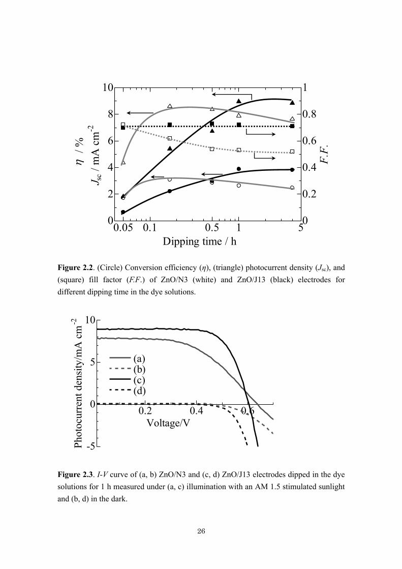
The change of conversion efficiency (η), photocurrent density (Jsc), and fill
factor (F.F.) of ZnO/N3 and ZnO/J13 electrodes for different soaking time in the dye
solutions is shown in Figure 2.2. While the voltages were almost unchanged, short
circuit current density (Jsc) initially increased on extension of the soaking time due to
increase of the adsorbed dye to improve the efficiency of light harvest. However, that of
ZnO/N3 creates a maximum of ca. 8.5 mA cm-2
at 10 min and begin to decrease, while

25
that of ZnO/J13 continues to increase and reaches a steady value of about 9 mA cm-2
.
On the other hand, fill factor (F.F.) of the ZnO/N3 cell continues to worsen, while that
of the ZnO/J13 cell is unchanged. As a consequence, the overall energy conversion
efficiency (η) of the ZnO/J13 cell increases proportionally to the increase of Jsc and
reaches a constant value of ca. 4%, whereas the highest efficiency of about 3% was
reached for that soaked in N3 for 10 min and got worse for the longer dipping time.
Worsening of the efficiency in the same trend, in fact even more seriously than the
present example, has been reported in combination of nanoparticulate ZnO electrode
with N3, and attributed to the overloading of the N3 dye to form aggregates [9].
Although such a problem of N3 could not be prevented by the use of electrodeposited
ZnO, J13 appears to behave better than N3, being less sensitive to the soaking time.
Figure. 2.3 compares the I-V curves of the ZnO/N3 and ZnO/J13 cells with the same
soaking time of 1 h. The most prominent difference is the F.F., being much worse for the
ZnO/N3 cell than ZnO/J13. The dark current of the ZnO/N3 cell is also much smaller
than ZnO/J13, indicating a significantly suppressed electron transfer to I3− ions in the
electrolyte.
26
Figure 2.2. (Circle) Conversion efficiency (η), (triangle) photocurrent density (Jsc), and
(square) fill factor (F.F.) of ZnO/N3 (white) and ZnO/J13 (black) electrodes for
different dipping time in the dye solutions.
Figure 2.3. I-V curve of (a, b) ZnO/N3 and (c, d) ZnO/J13 electrodes dipped in the dye
solutions for 1 h measured under (a, c) illumination with an AM 1.5 stimulated sunlight
and (b, d) in the dark.
0.2 0.4 0.6
-5
0
5
10
Voltage/V
Ph
oto
curr
ent
den
sity
/mA
cm
-2
(a) (b) (c) (d)
0.05 0.1 0.5 1 50
2
4
6
8
10
0
0.2
0.4
0.6
0.8
1
Dipping time / h
sc /
mA
cm
-2J
/ %
F.F.

27
The photocurrent action spectra of the ZnO/J13 and ZnO/N3 cells are shown in
Fig. 2.4. The maximum IPCEs of about 58% and 70% are reached at 510 nm on
ZnO/N3 and ZnO/J13 cells, respectively. IPCE is a product of the light harvesting
efficiency (LHE), the efficiency of charge separation on photoexcitation of dye bound to
ZnO (inj) and that of the collection of charge (coll),
IPCE = LHE × inj × coll (1)
For the cells measured here, LHE practically reaches its saturation at the wavelength of
light absorption maxima of these dyes. Since coll is expected to be the same for both
cells as they employ the same electrode materials and electrolyte, the lower inj of N3
should be responsible to the lower IPCE. Dye molecules adsorbed as aggregates do
absorb light but cannot inject electron to ZnO, so that inj of N3 becomes lower on
higher dye loading.
Figure 2.4. Photocurrent action spectra of the N3 (a) and J13 (b) cells employing ZnO
films soaked in the dye solutions for 1 h
28
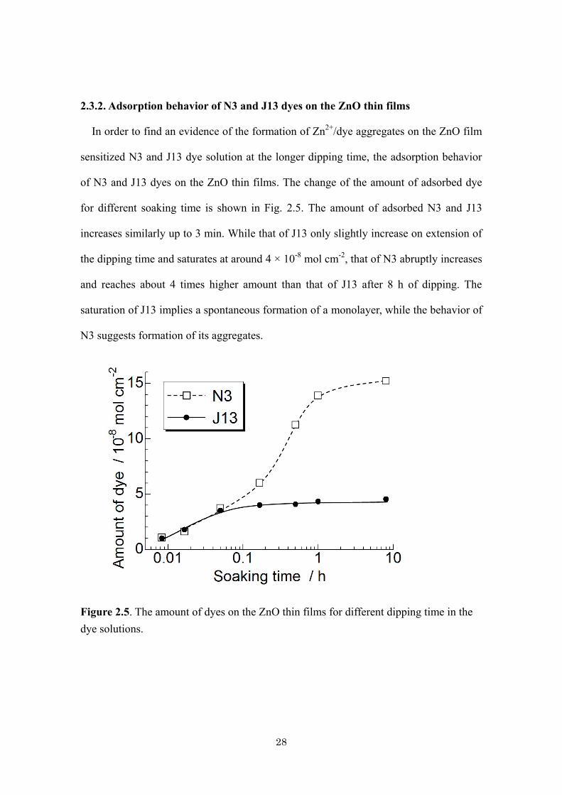
2.3.2. Adsorption behavior of N3 and J13 dyes on the ZnO thin films
In order to find an evidence of the formation of Zn2+
/dye aggregates on the ZnO film
sensitized N3 and J13 dye solution at the longer dipping time, the adsorption behavior
of N3 and J13 dyes on the ZnO thin films. The change of the amount of adsorbed dye
for different soaking time is shown in Fig. 2.5. The amount of adsorbed N3 and J13
increases similarly up to 3 min. While that of J13 only slightly increase on extension of
the dipping time and saturates at around 4 × 10⁻⁸
mol cm-2
, that of N3 abruptly increases
and reaches about 4 times higher amount than that of J13 after 8 h of dipping. The
saturation of J13 implies a spontaneous formation of a monolayer, while the behavior of
N3 suggests formation of its aggregates.
Figure 2.5. The amount of dyes on the ZnO thin films for different dipping time in the
dye solutions.

29
The apparent area occupied by a single dye molecule on the ZnO surface (Adye)
can be estimated from the amount of adsorbed dye (ndye) as calculated by equation (2),
Adye
ZnO
dyeNn
SA (2)
where NA is the Avogadro number (6.02 × 10²³
mol-1
) and SZnO is the total surface area
of porous ZnO thin film used in the experiments, which as determined as 3.87 × 10¹⁶
nm2 cm
-2 from the amount of adsorbed eosin Y and the ZnO surface area occupied by a
single eosin Y molecule (3.32 nm2 [19]) since eosin Y is known to undergo monolayer
adsorption on ZnO [18]. From nN3 and nJ13 after soaking for 8 h, AN3 and AJ13 are
calculated as 0.423 and 1.42 nm2, respectively. AN3 has been previously estimated as 1.6
nm2 for a monolayer of N3 on TiO2 [20]. Since the molecular structures of N3 and J13
are similar, similar values can be expected if monolayers of N3 and J13 are formed of
ZnO. The clearly smaller value estimated for N3 indicates its aggregation adsorbed as
multilayers and that of J13 close to 1.6 nm2 suggests a formation of a monolayer on
ZnO.
2.3.3. Surface analysis of the ZnO/dye electrode
The morphology of the porous ZnO thin films after dye adsorption for 3 min and
8 h has been observed by SEM (Fig. 6). The nanoporous structure of the
electrodeposited ZnO is preserved after 3 min dipping in J13 solution and the fine
structure was unchanged even after 8 h. On the other hand, the nanopores appear to be
closed by the aggregates of N3 already after 3 min, although similar amount of dyes
was found for N3 and J13 for this soaking time. After soaking the film for 8 h in N3, the
surface morphology completely changed. A thick (ca. 0.5 μm) layer of N3 aggregates
with featureless morphology is formed on top of the porous ZnO layer as recognized
from the cross section image of such a sample. No such layer is seen in case of J13. It is

30
evident that N3 dissolves ZnO and a randomly structured mixed aggregates of N3 and
Zn2+
sediments back on the outer surface of the porous ZnO, rather than forming a dye
multilayer [9, 21]. The surface of ZnO is not attacked by J13 since it behaves as a milder
acid than N3, and thus achieves a spontaneous formation of its monolayer on ZnO.
Figure. 2.6. Surface and cross section SEM images of ZnO thin films before dye
adsorption (a,b), after dipping for 3 min in J13 (c,d) and N3 (e,f) solution, and for 8 h in
J13 (g,h) and N3 (i,j) solution.
31
2.4. Conclusion
The J13 Ru(II)-complex has been evaluated as a sensitizer for ZnO solar cell in
comparison to the N3 dye. Analysis of the quantity of adsorbed dye as well as the
change of the surface morphology clearly indicated strong aggregation of N3, while J13
underwent spontaneous formation of a monolayer. As a consequence, Jsc of the N3 cell
creates a peak with a moderate time of dipping in the dye solution and it continues to
decrease with excessive dye adsorption as it leads to a loading of dye molecules not
directly bound to ZnO and thus cannot inject electron from its excited state. In addition,
extended dipping of ZnO in N3 solution resulted in a formation of a thick outer layer of
aggregates that hinder hole transport to significantly worsen F.F. None of such problems
were observed for J13, for which Jsc continued to increase to a steady value and F.F.
remained constant on extension of the dipping time. Although the efficiency of ca. 4%
eventually achieved with the J13 dye is not satisfactorily high as it is still worse than the
highest efficiency achieved for the ZnO solar cell in combination with organic dye
sensitizer, the present study clearly indicates the importance of the right chemistry
between ZnO and dye molecules to draw the best performance out of the system.
Tuning of the chemical property in addition to the energy structure is therefore an
important strategy to develop good photosensitizer for ZnO solar cells.
2.5 References
[1] B. O’Regan and M. Grätzel, Nature, 353, (1991) 737.
[2] M. Grätzel, Nature, 414, (2001) 338.
[3] Y. Chiba, A. Islam, Y. Watanabe, R. Komiya, N. Koide, and L. Han, Jpn. J. Appl.
Phys., 45, (2006) L638.
[4] M. K. Nazeeruddin, F. D. Angelis, S. Fantacci, A. Selloni, G. Viscardi, P. Liska, S.
Ito, B. Takeru, and M. Grätzel, J. Am. Chem. Soc., 127, (2005) 16835.
32
[5] E. Bellingeri, D. Marre, L. Pellegrino, I. Pallecchi, G. Canu, M. Vignolo, C.
Bernini, and A.S. Siri, Superlattices Microstruct., 38, (2005) 446.
[6] T. Yoshida, J. Zhang, D. Komatsu, S. Sawatani, H. Minoura, T. Pauporté, D.
Lincot, T. Oekermann, D. Schlettwein, H. Tada, D. Wöhrle, K. Funabiki, M.
Matsui, H. Miura, and H. Yanagi, Adv. Func. Mater., 19, (2009) 17.
[7] T. Yoshida, M. Iwaya, H. Ando, T. Oekermann, K. Nonomura, D. Schlettwein, D.
Wöhrle, and H. Minoura, Chem. Commun., (2004) 400.
[8] K. Keis, J. Lindgren, S. Lindquist, and A. Hagfeldt, Langmuir, 16 (2000) 4688.
[9] H. Horiuchi, R. Katoh, K. Hara, M. Yanagida, S. Murata, H. Arakawa, and M.
Tachiya, J. Phys. Chem. B, 107, (2003) 2570.
[10] K. Keis, E. Magnusson, H. Lindstrom, S. Lindquist, and A. Hagfeldt, Solar Energy
Materials and Solar Cells, 73, (2002) 51.
[11] D. P. Hagberg, T. Edvinsson, T. Marinado, G. Boschloo, A. Hagfeldt, and L. Sun,
Chem. Commun., (2006) 2245.
[12] S. Kim, J. K. Lee, S. O. Kang, J. Ko, J. H. Yum, S. Fantacci, F. De Angelis, D. Di
Censo, M. K. Nazeeruddin, and M. Grätzel, J. Am. Chem. Soc., 128, (2006) 16701.
[13] Z. Jin, H. Masuda, N. Yamanaka, M. Minami, T. Nakamura, and Y. Nishikitani, J.
Phys. Chem. C, 113, (2009) 2618.
[14] K. Ichinose, Y. Kimikado, and T. Yoshida, Electrochem., 79, (2011) 146.
[15] T. Tani, S. Kikuchi and K. Hosoya, Bull. Soc. Sci. Photography Jpn., 17, (1967) 24.
[16] S. Hori and T. Yoshida, Mater. Res. Soc. Symp. Proc., (2010) 1211-R03-40.
[17] R. Zhang, J. Pan, E. P. Briggs, M. Thrash, and L.L. Kerr, Sol. Energy Mater. Sol.
Cells, 92, (2008) 425.
[18] T. P. Chou, Q. Zhang., and G. Cao, J. Phys. Chem. C, 111, (2007) 18804.

33
Chapter 3. Size-controlled synthesis of SnO2 nanocrystals by microwave
hydrothermal reactions and their application for dye sensitized solar
cells
3.1. Introduction
Tin oxide (SnO2) has been regarded as an attractive material for use in gas sensors
[1], photocatalysts [2], electrochemical devices [3] and dye-sensitized solar cells
(DSSCs) [4]. In particular, nanosized SnO2 particles have become of much interest as
photoelectrode materials in high-performance DSSCs, owing to their high electron
mobility (125 cm2 V
-1 s
-1) [5] and high durability under a long term UV-irradiation[6].
In addition, their conduction band lying more positive potential than titanium dioxide
(TiO2) allows favorable charge separation for near infra-red absorbing dye sensitizers
having a relatively narrow HOMO-LUMO gap [7]. On the other hand, the
light-to-electricity conversion efficiency of SnO2-based DSSCs combined with dyes
absorbing in the visible range, such as Ru(II) polypyridyl complexes, is inferior to those
based on TiO2, not only due to the reduced voltage but also the significantly worsened
fill factor [8]. Such a poor device performance is caused by fast electron recombination
in SnO2 electrodes, as demonstrated by Green et al., so that back electron transfer rates
from SnO2 photoelectrodes to the redox shuttle are in a microsecond range while those
for TiO2 photoelectrodes are in a millisecond range [9]. In order to overcome such a
disadvantage, several groups tried to suppress the unwanted back electron transfer by
TiCl4 treatment on the surface of SnO2 particles [10, 11]. In addition, the structure
optimization for particle size and morphology is one of the promising routes to achieve
high efficiencies, as often realized for TiO2 or ZnO-based cells [12-15]. However, only a

34
little attention has been paid to the SnO2 nanostructure control as a strategy for
improving DSSCs performance, unlike a large number of reports found for TiO2 or ZnO
systems. In this regard, it is notable that Gubbala et al. reported enhanced photovoltage
of DSSCs employing one dimensional SnO2 nanowires as electrode materials [16]. Li et
al. also reported size-controlled SnO2 nanorod arrays to achieve 1D electron transport
being effective to decrease the number of grain boundaries, while reducing the
recombination reactions [17]. Very recently, Wang et al. employed micrometer-sized
hierarchical SnO2 particles composed of 30-40 nm nanocrystals for DSSCs [18]. It was
concluded that the secondary and primary SnO2 particle sizes give significant effects on
light scattering ability and electron transport properties resulting in the increase of
photocurrent. Even though a few examples can be mentioned as above, the knowledge
and understanding about the relationship between the structure, size of SnO2
nanoparticles and the DSSC function are limited.
Several groups reported size-controlled synthesis of SnO2 nanocrystals [19-21], in
which different crystal phase and morphology could be evolved by a post annealing
treatment of as-synthesized nanocrystals, typically at 200-800°C. The use of surfactants
or structure directing agents led to a successful size-tuning of SnO2 nanocrystals [22]. In
this thesis, a novel method to rapidly synthesize size controlled SnO2 nanocrystals by
microwave-assisted hydrothermal reaction employing chemical solutions in
ethanol/water mixed solvents is developed. Due to rapid and uniform heating of the
reaction solutions, the use of microwave radiation has significant advantages in
shortening processing time and promoting uniform nucleation of nanocrystals to
achieve narrow size distribution of SnO2 particles [21]. Moreover, the mixture of
ethanol and water allowed flexible control of crystallite size, owing to changes in

35
solubility of reaction intermediates is demonstrated. Dependence of DSSC performance
on SnO2 size was evaluated by means of current-voltage (I-V), incident
photon-to-current conversion efficiency (IPCE) measurements and stepped-light
induced transient measurements of photocurrent and voltage (SLIM-PCV). As a
consequence of the systematic study, it could improve maximum IPCE up to around
70% when N719 dye was employed, as achieved without any surface treatment of SnO2
electrodes.
3.2. Experimental
3.2.1. Synthesis and characterization of SnO2 nanocrystals
SnO2 nanocrystals were synthesized by a microwave-assisted hydrothermal
reaction in ethanol-water mixed solution containing SnCl4 as a Sn source. In a typical
synthesis, 0.05 or 0.5 M of SnCl4·5H2O (Wako) was dissolved in ethanol-water mixtures
in various ratios (0:1, 1:2, 2:1, or 10:1 in v/v) and was put in pressure withstanding
plastic reaction tubes to be set in a Milestone General MicroSYNTH reactor for 2.45
GHz microwave radiation at 1200 W, allowing controlled reaction temperature (180oC)
and period (45 minutes). The white precipitate resulting from the reaction was collected
by centrifugal separation at 10000 rpm for 10 minutes and was washed by water and
ethanol several times. Subsequently, the precipitate was dried at room temperature in air
over night to yield as-synthesized SnO2 powder. The SnO2 powder was characterized by
means of XRD (Rigaku Rint Ultima III X-ray diffractometer using Cu Kα radiation), a
Hitachi S-4800 field emission scanning electron microscope (FE-SEM) and a JEOL
JEM-2100 for high resolution transmission electron microscopic images (HR-TEM).
The surface area was determined from adsorption/desorption isotherms of N2 gas
36
employing the Brunauer-Emmet-Teller (BET) method using Micromeritics, TriStar II
surface area measurement system.
3.2.2. Preparation of SnO2 paste and film fabrication
SnO2 paste was prepared by adding 0.5 g of the synthesized SnO2 powder, 2 g of
terpineol (Aldrich) into 20 g of ethanol. Subsequently, 0.25 g of ethyl cellulose (10
wt%) solution was added. The ethyl cellulose solution in ethanol was prepared by
dissolving equal amount of two kinds of pure powders with different molecular weight
(in viscosity, 9-11 and 45-55 mPa s for 5wt% solution in toluene/ethanol = 80/20
mixture at 25˚C, Tokyo Chemical Industry). The mixture was ultrasonified 2 times, each
for 15 minutes by using Branson Sonifier 450 ultrasonic homogenizer. The mixture was
condensed to achieve ca. 20wt% for SnO2 content by removing ethanol by rotary
evaporator. The paste was coated by a doctor blade method onto F-doped SnO2 (FTO)
conductive glasses (10Ω/sq., Asahi Glass Asahi-DU) which was degreased
ultrasonically in detergent, acetone and rinsed with water. The thickness of the films
was adjusted to around 11 to 13 μm by varying thickness of Scotch tape attached to the
FTO glass as a spacer. The films were dried at 130oC for 5 min and were sintered at
500oC in air for 1 h.
3.2.3. Fabrication of DSSCs and evaluation of photovoltaic properties
The porous oxide photoelectrodes were sensitized by soaking them in a 300 μM
solution of N719 dye ( [RuL2(NCS)2]: 2 TBA, L= 2,2’-bipyridyl-4,4’-dicarboxylic acid,
TBA= tetra-n-butylammonium, Dyesol) in tert-butanol/acetonitrile (1/1 in volume) for
18 h. at room temperature. The light harvesting efficiency (LHE) of the photoelectrodes

37
were determined from the comparison of UV-Vis absorption spectra of bare and dyed
films measured in diffuse transmission mode employing a Hitachi 4100
spectrophotometer equipped with an integration sphere. The attenuation of the reflected
and strayed light is assumed to be proportional to that of the transmitted light. Sandwich
cells were configured by attaching the sensitized photoelectrode and a Pt-sputtered FTO
glass counter electrode in face-to-face using strips of Surlyn® film with 30 µm thickness
as spacers. Electrolyte solution consisting of 0.1 M LiI (Wako), 0.05 M I2 (Wako), 0.6
M 1,2-dimethyl-3-propylimidazolium iodide (DMPImI, Shikoku Chemicals Co.), and
0.5 M tert-butylpyridine (TBP, Nacalai Tesque) in acetonitrile was filled to the gap of
the electrodes by capillary action. I–V curves of the cells were measured by a
potentiostat equipped with a function generator (Hokuto Denko) under illumination
with a simulated sun light (AM 1.5, 100 mW cm−2
) generated by Yamashita-Denso,
YSS-150A. Photocurrent action spectra were measured on a Bunko-Keiki CEP-2000
system under monochromatic light illumination with a constant photon flux of 5.0×10¹⁵
s−1
cm−2
. The active area of the cells was regulated to 0.2 cm2 using a photomask. To
study the electron transport properties of the cells, electron diffusion coefficient and
electron lifetime were measured by stepped light induced transient measurements of
photocurrent and voltage, SLIM-PCV (EKO PSL-100-M) [23].
3.3. Results and Discussion
3.3.1. Synthesis and characterization of SnO2 nanocrystals
The effect of mixed solvent, ethanol-water as the reaction medium, on the
microwave synthesis of SnO2 nanoparticles was studied by systematically changing the
solvent ratio. Figure 3.1 shows XRD patterns of SnO2 nanoparticles synthesized by the

38
20 30 40 50 60 70 80
Inte
nsi
ty /
a.u
.
2 /degree (CuK)
SnO2 (JCPDS 41-1445)Sample holder
(11
0)
(20
0)(1
01
)
(21
1)
(22
0)
(00
2)
(31
0)
(11
2)
(20
2)
(32
1)
(b1)
(b2)
(b3)
(b4)
(b)
20 30 40 50 60 70 80
2 /degree
Inte
nsi
ty /
a.u
.
SnO2 (JCPDS 41-1445)Sample holder
(11
0)
(10
1)
(20
0) (2
11
)(2
20
)(0
22
)(3
10
)(1
12
)(3
01
)
(20
2)
(32
1)
(a1)
(a2)
(a3)
(a4)
(a)
20 30 40 50 60 70 80
Inte
nsi
ty /
a.u
.
2 /degree (CuK)
SnO2 (JCPDS 41-1445)Sample holder
(11
0)
(20
0)(1
01
)
(21
1)
(22
0)
(00
2)
(31
0)
(11
2)
(20
2)
(32
1)
(b1)
(b2)
(b3)
(b4)
(b)
20 30 40 50 60 70 80
2 /degree
Inte
nsi
ty /
a.u
.
SnO2 (JCPDS 41-1445)Sample holder
(11
0)
(10
1)
(20
0) (2
11
)(2
20
)(0
22
)(3
10
)(1
12
)(3
01
)
(20
2)
(32
1)
(a1)
(a2)
(a3)
(a4)
(a)
Figure. 3.1 XRD patterns of SnO2 powders synthesized by a microwave-assisted
hydrothermal reaction at 180oC for 45 min in different SnCl4 concentration (a) 0.5
M and (b) 0.05 M, by varying the solvent of the different ethanol-water ratio; (a1
and b1) 0:1, (a2 and b2) 1:2, (a3 and b3) 2:1, and (a4 and b4) 10:1.
reaction of 0.05 or 0.5 M SnCl4 solutions in water and ethanol-water mixture in
different ratios of 1:2, 2:1, and 10:1 (v/v). All samples show diffraction patterns
assigned to a single phase cassiterite SnO2 (PDF-2, entry 41-1445). The crystallite size
was estimated from the full width at half maxima (FWHM) of the (101) diffraction
peaks using Scherer’s equation and the values are summarized in Table 3.1. While only
tiny nanocrystals below 10 nm size is formed from aqueous solutions, the crystallite
size clearly increased by increasing the amount of ethanol content. Larger crystals were
obtained for the solutions with the higher SnCl4 concentration. The reaction yield was
practically 100% for all solutions as determined by weighing the dried precipitates. It
should however be noted that there was no product, when SnCl4 solution in dry ethanol
39
was employed, indicating the necessity of water for the hydrolysis of Sn4+
to produce
SnO2 nanocrystals.
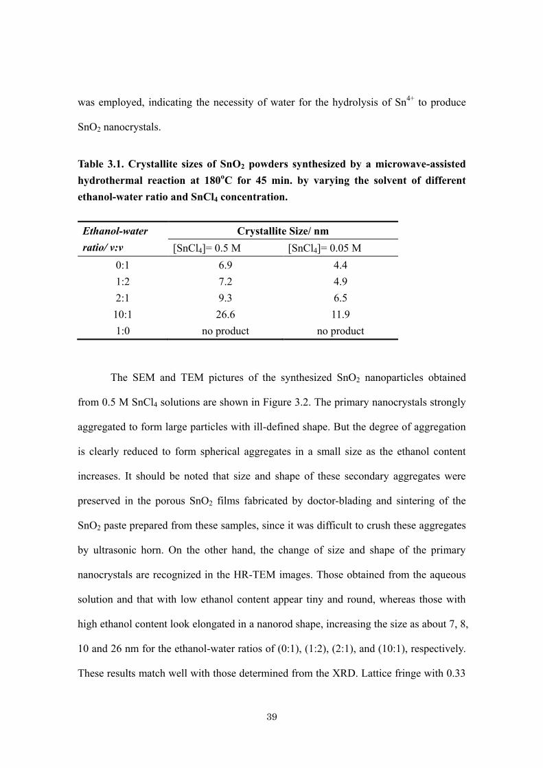
Table 3.1. Crystallite sizes of SnO2 powders synthesized by a microwave-assisted
hydrothermal reaction at 180oC for 45 min. by varying the solvent of different
ethanol-water ratio and SnCl4 concentration.
Ethanol-water
ratio/ v:v
Crystallite Size/ nm
[SnCl4]= 0.5 M [SnCl4]= 0.05 M
0:1 6.9 4.4
1:2 7.2 4.9
2:1 9.3 6.5
10:1 26.6 11.9
1:0 no product no product
The SEM and TEM pictures of the synthesized SnO2 nanoparticles obtained
from 0.5 M SnCl4 solutions are shown in Figure 3.2. The primary nanocrystals strongly
aggregated to form large particles with ill-defined shape. But the degree of aggregation
is clearly reduced to form spherical aggregates in a small size as the ethanol content
increases. It should be noted that size and shape of these secondary aggregates were
preserved in the porous SnO2 films fabricated by doctor-blading and sintering of the
SnO2 paste prepared from these samples, since it was difficult to crush these aggregates
by ultrasonic horn. On the other hand, the change of size and shape of the primary
nanocrystals are recognized in the HR-TEM images. Those obtained from the aqueous
solution and that with low ethanol content appear tiny and round, whereas those with
high ethanol content look elongated in a nanorod shape, increasing the size as about 7, 8,
10 and 26 nm for the ethanol-water ratios of (0:1), (1:2), (2:1), and (10:1), respectively.
These results match well with those determined from the XRD. Lattice fringe with 0.33
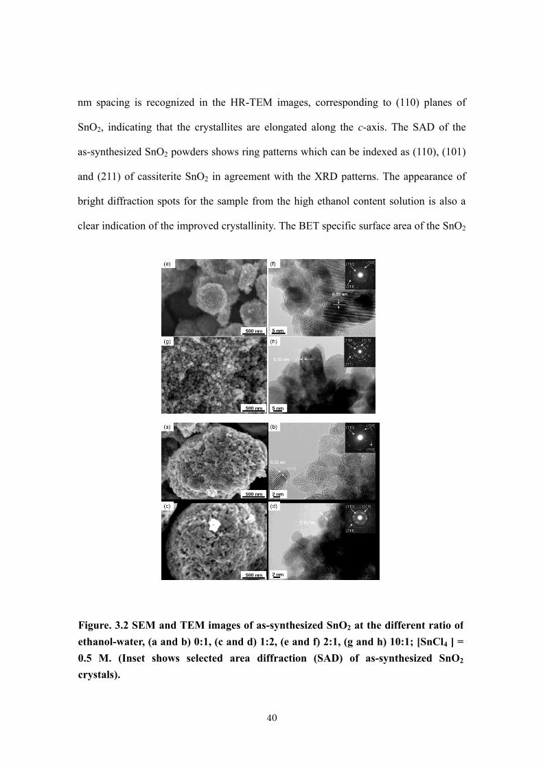
40
nm spacing is recognized in the HR-TEM images, corresponding to (110) planes of
SnO2, indicating that the crystallites are elongated along the c-axis. The SAD of the
as-synthesized SnO2 powders shows ring patterns which can be indexed as (110), (101)
and (211) of cassiterite SnO2 in agreement with the XRD patterns. The appearance of
bright diffraction spots for the sample from the high ethanol content solution is also a
clear indication of the improved crystallinity. The BET specific surface area of the SnO2
Figure. 3.2 SEM and TEM images of as-synthesized SnO2 at the different ratio of
ethanol-water, (a and b) 0:1, (c and d) 1:2, (e and f) 2:1, (g and h) 10:1; [SnCl4 ] =
0.5 M. (Inset shows selected area diffraction (SAD) of as-synthesized SnO2
crystals).
41
powders for the ethanol-water ratios of (0:1), (1:2), (2:1) and (10:1) were determined as
108.0, 108.1, 65.3 and 44.1 m3/g, respectively, which are in accordance with the change
of the crystallite size.
The mechanism for the increase of SnO2 crystal size can be explained by
considering the intermediate products as expressed by the following equations (eqs.1 -
4 ).
In water:
Sn4+
+ 4H2O Sn(OH)4 + 4H+ (1)
Sn(OH)4 SnO2 + 2H2O (2)
In ethanol/water:
Sn4+
+ 4C2H5OH Sn(OC2H5)4 + 4H+ (3)
Sn(OC2H5)4 + 2H2O SnO2 + 4C2H5OH (4)
In the presence of ethanol, ethoxide of Sn4+
can be formed as the reaction intermediate,
while hydrolysis of Sn4+
in the aqueous system should result in hydroxide that is
dehydrated to produce SnO2. The hydrolysis of the alkoxide results in the formation of
SnO2 (eq. (4)), indicating that the presence of water is essential. The solubility of the
intermediate alkoxide, Sn(OC2H5)4 in ethanol/water, is supposed to be much higher than
Sn(OH)4 in water [24]. Thus, the reversal of the reaction expressed by eq. (4) leads to a
dissolution of SnO2 during the course of the crystal growth. Such a dissolution /
recrystallization sequence in the case of the water-ethanol mixture can promote the
ripening of SnO2 crystals. It is also important to note that the addition of ethanol in the
reaction mixture at a high amount was useful to suppress aggregation of the
nanocrystals probably due to the change of surface charge of SnO2.
42
We also studied the influence of SnCl4 concentration on the crystal size, while
fixing the ethanol-water ratio as 10:1. The particle size increased from around 11 nm to
26 nm with increasing the concentration of SnCl4 from 0.05M to 0.5 M as shown in
Figure 3.3. It appears that the large amount of SnCl4 does not influence the number of
nuclei formed in the reaction mixture very much, while that enhances the rate of the
SnO2 growth leading to the formation of large crystals. In other words, crystal sizes can
be controlled by changing the concentration of SnCl4 in the ethanol-water mixture
solution. We analyzed the size distribution of SnO2 nanoparticles from SEM images as
shown in Figure 3.3. The size distribution diagrams clearly indicate a relatively narrow
Figure 3.3. SEM images and size distribution diagrams of SnO2 nanoparticles
prepared by a microwave-assisted hydrothermal method at 180°C for 45 min
with different concentration of SnCl4, (a) 0.05 M, (b) 0.10 M, and (c) 0.50 M. The
reaction solvent is ethanol-water ratio of 10:1 (v/v).

43
distribution of each particle synthesized by a microwave synthesis. Average particle
sizes for the sample a, b, and c are 11.2, 18.4 and 26.2 nm, respectively.
3.3.2. Application of SnO2 nanocrystals as photoelectrode materials of DSSCs
We employed the synthesized SnO2 particles to prepare porous films to test
them as photoelectrode in DSSCs. Strongly aggregated samples either showed very
poor performance or made it difficult to produce mechanically strong films. Films
prepared from well-dispersed samples with different crystallite size are therefore
compared here, namely those from ethanol-water = 10:1 baths with the varied
concentration of SnCl4. I-V curves of DSSCs are shown in Figure 3.4. Despite of their
similar film thickness in the range of 11-13 μm, the device performance is clearly
improved with increasing the size of SnO2 crystals. The use of large SnO2 crystals can
increase all values of short circuit photocurrent (Jsc), photovoltage (Voc) and fill factor
(FF) as listed in Table 3.2. The highest energy conversion efficiency of 1.35% was
0 0.1 0.2 0.3 0.40
2
4
6
8
10
Photo
curr
ent
den
sity
/ m
A.c
m-2
Voltage/V
(a)
(b)
(c)
Figure. 3.4. Current-voltage curves of DSSCs based on SnO2 photoelectrode films
consisted of SnO2 nanocrystals with (a) 11 nm, (b) 18 nm, and (c) 26 nm in size.

44
reached for the cell employing the SnO2 crystals of 26 nm in size. A relatively low
efficiency compared to those of other reports [10, 11, 18] is probably due to no surface
treatments, such as TiCl4 treatment, applied for our devices. We believe that the surface
passivation approach would improve the energy conversion efficiency of the present
devices.
Figure 3.5 shows the photocurrent action spectra of these cells in incident photon
to current efficiency (IPCE). The highest IPCE at 530 nm (at the maximum of light
absorption by N719) for the sample a, b, and c were 32.7, 47.6, and 67.6%, respectively.
As the LHE spectra were measured separately for these samples, the absorbed photon to
current efficiency (APCE) can be estimated from the eq. 5.
Table 3.2. I-V parameters of DSSCs consisting of different size SnO2 nanocrystals.
Sample Crystallite
size /nm
Jsc/ mA.cm-2 Voc/V FF η/% IPCE/%
(530 nm)
APCE/%
(530 nm)
a 11 4.66 0.295 0.27 0.37 32.7 35.2
b 18 5.72 0.321 0.36 0.66 47.6 49.0
c 26 8.02 0.345 0.49 1.35 67.6 73.5
400 500 600 700 8000
20
40
60
80
IPC
E/%
Wavelength/nm
(a)
(b)
(c)
Figure 3.5. IPCE spectra of DSSCs based on SnO2 films prepared using different
size SnO2 nanocrystals with (a) 11 nm (b) 18 nm and (c) 26 nm in size.

45
IPCE = LHE × APCE (5)
The LHE values were similar for these samples (92.9, 97.1 and 92.0% at 530 nm for a,
b and c, respectively). As a result, the values of APCE followed the same order as IPCE,
achieving the highest APCE of 73.5% for the sample c (Table 3.2). It is obvious that the
difference of LHE does not account for the changes of IPCE. APCE is the product of
electron injection efficiency from excited dye molecules to SnO2 (ηinj) and electron
collection efficiency (ηcoll) of the photoelectrode. Since the large difference of ηinj
cannot be anticipated for the same combination of SnO2 and N719 dye, the
improvement of ηcoll should be responsible for the increase of APCE on increasing the
crystal size.
For comparison, we evaluated DSSCs employing a commercially available TiO2
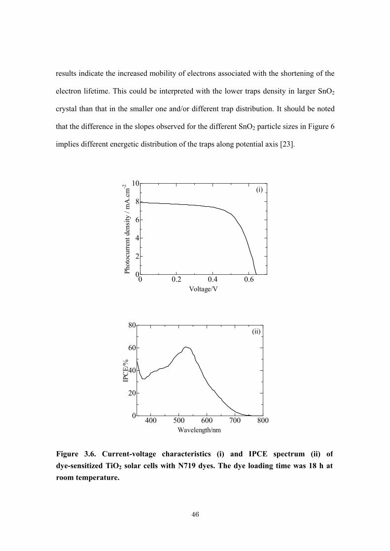
paste. I-V curve and IPCE spectra of TiO2 based DSSCs employing N719 dye is shown
in Figure 3.6. We found that the photocurrent density for SnO2 based cells is slightly
higher than that of TiO2 cell. The maximum IPCE for TiO2 based cells was about 62 %
(λmax = 530 nm) without TiCl4 treatment for TiO2 surface. In fact, the optimized IPCE of
about 63 % of TiO2 based cells without TiCl4 surface treatment have been reported [25].
The conduction band level of SnO2 lying more positive than that of TiO2 could facilitate
a favorable electron injection from the LUMO of N719 to the conduction band of SnO2.
In order to further understand photovoltaic properties of SnO2-based DSSCs, we
determined electron diffusion coefficients (D) and electron lifetimes (τ) by a SLIM-PCV
method. Figure 6 shows plots of D and τ against the electron density determined by
charge extraction measurement, while Figure 7 shows the relationship between Voc and
electron density. It turned out that the faster electron diffusion is observed for larger
SnO2 crystal and the electron lifetime becomes shorter for a given electron density. The
46
results indicate the increased mobility of electrons associated with the shortening of the
electron lifetime. This could be interpreted with the lower traps density in larger SnO2
crystal than that in the smaller one and/or different trap distribution. It should be noted
that the difference in the slopes observed for the different SnO2 particle sizes in Figure 6
implies different energetic distribution of the traps along potential axis [23].
0 0.2 0.4 0.60
2
4
6
8
10
Photo
curr
ent
den
sity
/ m
A.c
m-2
Voltage/V
(i)
400 500 600 700 8000
20
40
60
80
IPC
E/%
Wavelength/nm
(ii)
Figure 3.6. Current-voltage characteristics (i) and IPCE spectrum (ii) of
dye-sensitized TiO2 solar cells with N719 dyes. The dye loading time was 18 h at
room temperature.

47
1018 101910-6
10-5
abc
Electron density / cm-3
Dif
fusi
on
coef
fici
ent
(D)
/ cm
2 s
-1
1018 101910-6
10-5
abc
Electron density / cm-3
Dif
fusi
on
coef
fici
ent
(D)
/ cm
2 s
-1
1018 101910-2
10-1
100
101
Ele
ctro
n l
ifet
ime
(τ)
/ s
Electron density / cm-3
abc
(ii)
1018 101910-2
10-1
100
101
Ele
ctro
n l
ifet
ime
(τ)
/ s
Electron density / cm-3
abc
1018 101910-2
10-1
100
101
Ele
ctro
n l
ifet
ime
(τ)
/ s
Electron density / cm-3
abc
(ii)
Figure 3.7. Plot of (i) electron diffusion coefficients and (ii) electron lifetimes
vs electron density in dye-sensitized SnO2 solar cells employing different size
SnO2 nanocrystals with (a) 11 nm (b) 18 nm and (c) 26 nm in size.
1018 10190
100
200
300
400
Voc
/ m
V
Electron density / cm-3
abc
1018 10190
100
200
300
400
Voc
/ m
V
Electron density / cm-3
abc
Figure 3.8 Open circuit voltages of dye-sensitized solar cells as a function of
electron density employing different size SnO2 nanocrystals with (a) 11 nm
(b) 18 nm and (c) 26 nm in size.

48
Moreover, the plots in Figure 3.8 indicate the clear shift of their positions along
the potential axis. One possible explanation is the change of flatband potential.
However, the shift of flatband potential as much as 200 mV is unlikely since our
crystallographic analysis did not reveal large differences except the crystal sizes.
Therefore, it is postulated that their differences come from the electron trap density and
distribution. In order to understand the increased photovoltages with increasing particle
sizes, we tested I-V measurements of the cells under dark conditions as shown in Figure
3.9. The results show that the dark current decreases with increasing SnO2 particle sizes.
The high density of traps is expected for tiny SnO2 particles at the surface could
facilitate back electrons transfers to oxidized species in the electrolyte through surface
states. In other words, this lead to the higher recombination rate of electrons for smaller
particles compared to those lower traps density for the larger particles. As a
consequence, the largest crystals obtained in the present study achieved the highest Voc
as well as the improved fill factor.
0 0.1 0.2 0.3 0.4-5
-4
-3
-2
-1
0
Ph
oto
curr
ent
den
sity
/ m
A.c
m-2
Voltage/V
(a)
(b)
(c)
Figure 3.9. Current-voltage curves of DSSCs based on SnO2 photoelectrode films
under dark conditions. DSSCs of SnO2 nanocrystals with (a) 11 nm, (b) 18 nm,
and (c) 26 nm in size are presented.

49
3.4. Conclusion
The size-controlled synthesis of SnO2 nanocrystals via a microwave
hydrothermal reaction in a mixed ethanol-water and SnCl4 solution was demonstrated.
Ethanol dominant composition of the reaction medium was found to be useful to
promote the crystal growth owing to the increased solubility of the reaction
intermediates. It was also found that increased SnCl4 concentration further contributes
to the increase of the crystal size as well as avoiding aggregation of the particles. Porous
SnO2 electrodes employing thus prepared large SnO2 particles exhibited a decent
performance as photoelectrodes of DSSCs, resulting in an IPCE of about 70% with
N719 dye, whereas those employing aggregated small particles turned out to be very
poor. SLIM-PCV analysis suggested that their differences in electron trap density and
distribution could rationalize the observed differences of photoelectrochemical
behavior.
3.4. References
[1] A. Cabota, A. Diegueza, A. Romano-Rodrigueza, J.R. Morantea, N. Barsanb,
Sensors and Actuators B, (2001), 79, 98.
[2] Y. Han, X. Wu, Y. Ma, L. Gong, F. Qua, H. Fan, Cryst. Eng.Commun., (2011), 13,
3506.
[3] H. Wang, Q. Liang, W. Wang, Y. An, J. Li, L. Guo, Crys. Growth Des., (2011), 11,
2942.
[4] Y. F. Wang, J. W. Li, Y. F. Hou, X.Y. Yu, C. Y. Su, D. B. Kuang, Chem. Eur. J.,
(2010), 16, 8620-8625.
[5] E. N. Kumar, R. Jose, P. S. Archana, C. Vijila, M. M. Yusof, S. Ramakrishna,
Energy. Environ. Sci., (2012), 5, 5401.
[6] M.K.I. Senevirathna, P.K.D.P. Pitigala, E.V.A. Premalal, K. Tennakone, G.R.A.
Kumara, A. Konno, Sol. Energ. Mat. and Solar Cells, , (2007), 91, 544.
50
[7] S. Gubbala, V. Chakrapani, V. Kumar, M.K. Sunkara, Adv.Fun.. Mater., (2008), 18,
2411.
[8] A. Birkel, Y. G. Lee, D. Koll, X. V. Meerbeek, S. Frank, M. J. Choi, Y. S. Kang, K.
Char, W. Tremel, Energy Environ. Sci., (2012), 5, 5392.
[9] A. N. M. Green, E. Palomares, S. A. Haque, J. M. Kroon, J. R. Durrant, J. Phys.
Chem. B, (2005), 109, 12525.
[10] P. Zhu, M. V. Reddy, Y. Wu, S. Peng, S. Yang, A.S. Nair, K. P. Loh, B.V.R.
Chowdari, S. Ramakrishna, Chem. Commun., (2012), 48, 10865.
[11] Y. F. Wang, J. Li, Y.F. Hou, X. Y. Yu, C. Y. Su, D.B. Kuang, Chem. Eur. J.,
(2010), 16, 8620.
[12] S. Nakade, Y. Saito, W. Kubo, T. Kitamura, Y. Wada, S. Yanagida, J . Phys. Chem.
B, (2003), 107, 8607
[13] T.P. Chou, Q. Zhang, B. Russo, G.E. Fryxell, G. Cao, J. Phys. Chem. C , (2007),
111, 6296
[14] Z. Xue, W. Zhang, X. Yin, Y. Cheng, L. Wanga, B. Liu, RSC Adv., 2012, 2, 7074
[15] T.T. Chu, H. Jiang, L.W. Ji, W. S. Shih, J. Zhong, M.J. Zhuang, Microelectronics J.,
(2009), 40, 50
[16] S. Gubbala, H.B. Russell, H. Shah, B. Deb, J. Jasinski, H. Rypkema, M. K.
Sunkara, Energy Environ. Sci., (2009), 2, 1302.
[17] Y.Li. Wang, M. Guo, M. Zhang, Xi.D. Wang, Crys.Eng. Commun., 2010, 12, 4024
[18] Y.F. Wang, K.N. Li, C.L. Liang, Y.F. Hou, C.Y. Sua, D.B. Kuang, J. Mater.
Chem., (2012), 22, 21495
[19] H.J. Ahn, H.C. Choi, K.W. Park, S.B. Kim, Y.E. Sung, J. Phys. Chem. B, (2004),
108, 9815.

51
[20] P. Koshy, J. T. Abraham, P. S. Mukherjee, V. K. Vaidyan, Phys. Sta. Sol.(a),
(1997), 161, 399.
[21] P. G. Mendes, M. L. Moreira, S. M. Tebcherani, M. O. Orlandi, J. Andres, M. S. Li,
N. D. Mora, J. A. Varela, E. Longo, J Nanopart. Res, (2012), 14, 750
[22] V. Rajendran, K. Anandan, Materials Science in Semiconductor Processing, (2012),
15, 393.
[23] Y. Fukai, Y. Kondo, S. Mori, E. Suzuki, Electrochem. Commun., (2007), 9, 1439
[24] X. Xia, X. J. Dong, Q. F. Wei, Y. B. Cai, K. Y. Lu, Express Polymer Letters, (2012),
6, 169.
[25] P.M. Sommeling, B. C. O`Regan, R. R. Haswell, H. J. P. Smit, N. J. Bakker, J.
Phys. Chem. B, (2006), 110, 19191.
52
Chapter 4. Tandem dye-sensitized solar cells consisting of ZnO and SnO2 based
photoelectrodes
4.1. Introduction
Dye-sensitized solar cells (DSSCs) based on titanium dioxide (TiO2) porous
electrode with conversion efficiency (η) of over 12% have been reported in 2012 [1].
However, the efficiency of dye sensitized solar is relatively lower compared to
conventional solar cells. The main reason for that is the lack of light harvesting of the
lower energy photons from solar light. One of attempts to improve the performance of
DSSCs is development of tandem dye-sensitized to expand the photo-response into
near-IR region. There have been reported on tandem DSSCs where two single cells are
combined in one structure of cell [2-9]. T-DSSCs consisting of a top cell (FTO
glass/TiO2 stained by a Ru- dye (N719)/electrolyte layer/FTO glasses) and a bottom cell
(FTO glass/TiO2 stained by a Ru dye (black dye)/electrolyte layer/FTO glasses) has
been reported [3]. Murayama et al., (2008) has demonstrated the increase of the
photocurrent of TiO2 based tandem DSSCs compared to each single junction cell [4].
Most T-DSSCs reported so far has relied on the use of TiO2 based photoelectrodes. In
this chapter, the new structure of T-DSSCs consist of ZnO/J13 and SnO2/IR-820
photoelectrodes as top and bottom cells of T-DSSCs respectively is assembled and their
cell properties are analyzed by I-V and IPCE measurements.
4.2. Experiment
4.2.1. Fabrication of top cell, bottom cell and T-DSSCs
For the top cell, ZnO/J13 photoelectrodes based DSSCs were fabricated as follow,

53
electrodeposited porous ZnO thin films were sensitized by soaking them in 0.5 mM J13
dye solutions in tert-buthyl alcohol/dimetyl formamide (v/v = 1/1) mixture, at 60ºC for
1 h. The dyed ZnO electrode and a Pt-sputtered FTO glass counter electrode were
assembled into a cross-shape-type (0.28 cm2 in area) cell using a hot-melt ionomer film
of 30 m in thickness as a spacer. Electrolyte solution consisting of 0.1 M LiI (Wako),
0.05 M I2 (Wako), 0.6 M 1,2-dimethyl-3-propylimidazolium iodide (Shikoku), 0.5 M
tert-butylpyridine (TBP, Nacalai tesque) in acetonitrile was filled by capillary action.
For the bottom cell, SnO/IR-820 photoelectrodes based DSSCs were fabricated as
follow, porous SnO2 thin films were sensitized by soaking them in 0.1 mM IR-820 dye
( Sigma Aldrich) solutions in ethanol, at 60ºC for 24 h. The dyed SnO2 electrode and a
Pt-sputtered FTO glass counter electrode were assembled into a cross-shape-type (0.3
cm2 in area) cell using a hot-melt ionomer film of 30 m in thickness as a spacer.
Electrolyte solution consisting of 0.1 M LiI (Wako), 0.05 M I2 (Wako), 0.6 M
1,2-dimethyl-3-propylimidazolium iodide (Shikoku), 0.5 M tert-butylpyridine (TBP,
Nacalai tesque) in acetonitrile was filled by capillary action. T-DSSCs were fabricated
by series connected of top and bottom cells.
4.2.2. Cells properties measurements
I–V curves of the cells were measured by a Bunko-Keiki CEP-2000 system under
illumination with a simulated sun light (AM 1.5, 100 mW cm−2
). Photocurrent action
spectra were measured on the same system under monochromatic light illumination
with a constant photon flux of 5.0×10¹⁵
s−1
cm−2
. The active area of the cells was
regulated to 0.2 cm2 using a photomask.

54
4.3. Result and discussion
4.3.1. Absorbance spectra of dye solutions
The molecular structure and absorption spectra of J13 dye and IR-820 dye is
shown in Figure 4.1 and 4.2 respectively. The absorption spectra of both two dyes show
their different wavelength light absorption. The J13 dye absorb in visible light from 350
to 700 nm, while the IR-820 dye absorb in near-infrared light from 600 to 900 nm.
(a) (b)
Figure 4.1. Molecular structure of (a) J13 and (b) IR-820 dyes.
400 600 800 10000
1
2
3
4
Wavelength/nm
Abso
rbance
J13 IR-820
Figure 4.2. Absorption spectra of J13 and IR-820 dyes in dimethyl formamide (DMF)
and ethanol solution respectively.
N
N
COOH
HOOC
N
NNRu O
C4H9
NCSSCN
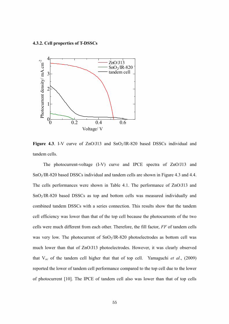
55
4.3.2. Cell properties of T-DSSCs
0 0.2 0.4 0.60
1
2
3
4 ZnO/J13 SnO2/IR-820 tandem cell
Photo
curr
ent
den
sity
/ m
A.c
m-2
Voltage/ V
Figure 4.3. I-V curve of ZnO/J13 and SnO2/IR-820 based DSSCs individual and
tandem cells.
The photocurrent-voltage (I-V) curve and IPCE spectra of ZnO/J13 and
SnO2/IR-820 based DSSCs individual and tandem cells are shown in Figure 4.3 and 4.4.
The cells performances were shown in Table 4.1. The performance of ZnO/J13 and
SnO2/IR-820 based DSSCs as top and bottom cells was measured individually and
combined tandem DSSCs with a series connection. This results show that the tandem
cell efficiency was lower than that of the top cell because the photocurrents of the two
cells were much different from each other. Therefore, the fill factor, FF of tandem cells
was very low. The photocurrent of SnO2/IR-820 photoelectrodes as bottom cell was
much lower than that of ZnO/J13 photoelectrodes. However, it was clearly observed
that Voc of the tandem cell higher that that of top cell. Yamaguchi et al., (2009)
reported the lower of tandem cell performance compared to the top cell due to the lower
of photocurrent [10]. The IPCE of tandem cell also was lower than that of top cells
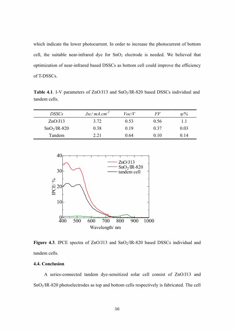
56
which indicate the lower photocurrent. In order to increase the photocurrent of bottom
cell, the suitable near-infrared dye for SnO2 electrode is needed. We believed that
optimization of near-infrared based DSSCs as bottom cell could improve the efficiency
of T-DSSCs.
400 500 600 700 800 900 10000
10
20
30
40
IPC
E/
%
Wavelength/ nm
ZnO/J13 SnO2/IR-820 tandem cell
Figure 4.3. IPCE spectra of ZnO/J13 and SnO2/IR-820 based DSSCs individual and
tandem cells.
4.4. Conclusion
A series-connected tandem dye-sensitized solar cell consist of ZnO/J13 and
SnO2/IR-820 photoelectrodes as top and bottom cells respectively is fabricated. The cell
Table 4.1. I-V parameters of ZnO/J13 and SnO2/IR-820 based DSSCs individual and
tandem cells.
DSSCs Jsc/ mA.cm-2
Voc/V FF η/%
ZnO/J13 3.72 0.53 0.56 1.1
SnO2/IR-820 0.38 0.19 0.37 0.03
Tandem 2.21 0.64 0.10 0.14

57
performance of individual and tandem cells is evaluated. The performance of tandem
cell was lower than that of top cell due to the lower of photocurrents as well as FF. It
should be noted that by this combination, the open-circuit photovoltage of
series-connected tandem DSSCs was higher than that of the top cell.
4.5. References
[1] A. Yella, H.W. Lee, H.N. Tsao, C. Yi, A.K. Chandiran, M.K. Nazeeruddin,
E.W.G.Diau, C.Y. Yeh, S.M. Zakeeruddin, M. Gratzel, Science, (2011), 334, 629.
[2] P. Liska, K. R. Thampi, M. Grätzel, D. Brémaud, D. Rudmann, H. M. Upadhyaya, A.
N. Tiwari, Applied Physics Letters, (2006), 88(20): 203.
[3] K.Uzaki, S. S. Pandey, S. Hayase, Journal of Photochemistry and Photobiology A:
Chemistry, 216, (2010), 104.
[4] M. Murayama, T. Mori, Thin Solid Films, 516, (2008), 2716.
[5] W. Kubo, A. Sakamoto, T. Kitamura, Y. Wada, S. Yanagida, Journal of
Photochemistry and Photobiology A: Chemistry , 164 (2004) 33.
[6] A. Nattestad, M. Ferguson, R. Kerr, Y. B. Cheng, U. Bach, Nanotechnology, 19
(2008) 295304.
[7] D. Xiong, W. Chen, Front. Optoelectron. (2012), 5(4), 371.
[8] J. He, H. Lindstrom, A. Hagfeldt, S. E. Lindquist, Solar Energy Materials & Solar
Cells, 62, (2000) 265.
[9] S. K. Balasingam, M. Lee, M. G. Kang, Y. Jun, Chem. Commun., (2013), 49, 1471
[10] T. Yamaguchi, Y. Uchida, S. Agatsuma, H. Arakawa, Solar Energy Materials &
Solar Cells, 93 (2009) 733.
58
Chapter 5. Conclusions
Results obtained throughout this study include several important findings to
explore the advantages of metal oxide/dye composite material as photoelectrodes for
tandem DSSCs.
The ZnO DSSCs coupled with a novel Ru-complex, J13 dye, gave an IPCE
maximum of about 70 % at 510 nm. Adsorption behavior and surface shape analysis
revealed that the formation of the Zn2+
/dye aggregates on the ZnO film sensitized J13
dye solution could be significantly reduced compared to the standard N3 dye solution
for a longer dipping time. The reduction of aggregates resulted in higher electron
injection efficiency from excited dyes to the ZnO conduction band so that the better
performance is achieved. Results suggested that J13 dye is more suitable than that of N3
dye for ZnO-based DSSCs. The optimization of the molecule structure of J13 dye is in
progress to search for the best sensitizers for ZnO solar cells.
A new synthetic method to rapidly produce size-tunable SnO2 nanocrsytals was
established in this study. The size was successfully adjusted by a microwave-assisted
hydrothermal reaction at 180oC for 45 minutes in a mixed solvent ethanol-water system.
DSSCs incorporating with the SnO2 nanocrystals as photoelectrode materials
demonstrated that the light-to-electricity conversion efficiency can be increased with
increasing the size of SnO2 nanocrystals mainly due to the enhancement of
photocurrents and fill factors. It should be noted that the quantum efficiency achieves
around 70 % (λmax=530nm) when N719 is employed. The size dependent difference of
photoelectrochemical properties is studied by SLIM-PCV measurements. The results
indicate a fast electron transport with the large SnO2 crystals, owing to the small
electron trap density and its shallow distribution.

59
A new design of tandem dye-sensitized solar cell consist of ZnO/J13 and
SnO2/IR-820 photoelectrodes as top and bottom cells respectively is fabricated.
Evaluation of series-connected tandem cell performances shows that the voltage is
higher than that of the top and the bottom cells. In order to improve the efficiency of
T-DSSCs, the optimization of near-infrared based DSSCs should be needed.
60
Publication List
1. Aggregation behavior of differently substituted Ru(II)-complex dyes as sensitizer for
electrodeposited ZnO solar cells
Journal of Photochemistry and Photobiology A: Chemistry, 242 (2012) 67-71
Asdim, Keigo Ichinose, Tomohiko Inomata, Hideki Masuda, Tsukasa Yoshida
2. Microwave synthesis of size-controllable SnO2 nanocrystals for dye-sensitized
solar cells
New Journal of Chemistry, 2014, 38, 598-603
Asdim, Kazuhiro Manseki, Takashi Sugiura, Tsukasa Yoshida

61
Acknowledgment
During my PhD study time at Gifu University, I have learned great things not
only about science and academics, but also about the life, the truth and the faith. In large
part of my time here was made enjoyable due to supports and helps from many people.
In this moment, I would like to thank all the people supporting me in many ways to
make where I am today.
First of all, I would like to express my greatest appreciation to my two advisors,
Sugiura sensei and Yoshida sensei for all the guidance, supports, and helps during my
study. I also would like to express my greatest appreciation to Manseki-sensei who
always support and help me for my PhD thesis preparation. I also thank to Matsui sensei
as a committee chair and Funabiki sensei as a committee member of my PhD degree
examination for all suggestion and helpful comments for future research. I also would
like to thank to Kobayashi sensei as a leader in Environmental and Renewable Energy
System (ERES) Division for supporting and helping me especially in the beginning of
my study. I also want to thank to all member of our laboratory who have helped and
supported me when I faced many problems in my research. In this great moment, I
deeply appreciate my mother, my wife, my son who always prayed for my study. Their
love and patient make me become strong and improve my motivation to finish my study
here. I also would like to special thanks to Indonesian Government for financial support
and give me the chance to study in Japan.

62


![Morphological and Optical Properties of SnO2 Doped ZnO ... · The structural, optical, and electronic properties are determined by the particle size [3,4]. SnO 2 and ZnO are belonging](https://img.dokumen.tips/doc/110x75/5f81daa8eb6da10c0c76a647/morphological-and-optical-properties-of-sno2-doped-zno-the-structural-optical.jpg)