Embed Size (px)
Citation preview

TIMING AND CONGESTION DRIVEN ALGORITHMS FOR FPGA PLACEMENT
Yue Zhuo
Thesis Prepared for the Degree of
MASTER OF SCIENCE
UNIVERSITY OF NORTH TEXAS
December 2006
APPROVED: Hao Li, Major Professor Farhad Shahrokhi, Committee Member Shengli Fu, Committee Member Armin R Mikler, Departmental Coordinator of
Graduate Studies Krishna Kavi, Chair of the Department of
Computer Science and Engineering Oscar Garcia, Dean of the College of
Engineering Sandra L. Terrell, Dean of the Robert B.
Toulouse School of Graduate Studies

Zhuo, Yue, Timing and Congestion Driven Algorithms for FPGA Placement. Master of
Science (Computer Engineering), December 2006, 71 pp., 7 tables, 28 illustrations, references,
64 titles.
Placement is one of the most important steps in physical design for VLSI circuits. For
field programmable gate arrays (FPGAs), the placement step determines the location of each
logic block. I present novel timing and congestion driven placement algorithms for FPGAs with
minimal runtime overhead. By predicting the post-routing timing-critical edges and estimating
congestion accurately, this algorithm is able to simultaneously reduce the critical path delay and
the minimum number of routing tracks. The core of the algorithm consists of a criticality-history
record of connection edges and a congestion map. This approach is applied to the 20 largest
Microelectronics Center of North Carolina (MCNC) benchmark circuits. Experimental results
show that compared with the state-of-the-art FPGA place and route package, the Versatile Place
and Route (VPR) suite, this algorithm yields an average of 8.1% reduction (maximum 30.5%) in
the critical path delay and 5% reduction in channel width. Meanwhile, the average runtime of the
algorithm is only 2.3X as of VPR.

ACKNOWLEDGMENTS
I have been fortunate to have my parents over the past 28 years. They always support
me whenever I was ambitious or in depression. Without them, I can never be strong enough
to stand success and failure. I dedicate this thesis to them.
I joined the department of computer science and engineering of UNT in Fall 2005. From
that moment, I received great help from a lot of professors and friends. Dr. Hao Li is my
major professor who taught me a lot in the field of VLSI CAD. His encouragement and
invaluable advice really motivated me to work hard on research and this thesis.
Dr. Farhad Shahrokhi, who impressed me by his profound knowledge, gave me a lot of
insight into graph theory. He spent much time attending the events hosted by the Chinese
Student and Scholar Association. Dr. Phil Sweany, Dr. Paul Tarau, and Dr. Armin
R. Mikler improved my understanding of compiler, programming languages and operating
system. Dr. Saraju P. Mohanty shared tips of writing a paper with me. I am grateful to all
of them.
I also appreciate my friends who helped me and shared my happiness. I am thankful to
Jerry, Harry, Xiaohui, Kevin, Yohan, Yomi, Toby,.... My friends are my great fortune. I will
never forget this precious period we enjoyed together.
ii
CONTENTS
ACKNOWLEDGMENTS ii
LIST OF TABLES v
LIST OF FIGURES vi
CHAPTER 1. INTRODUCTION 1
1.1. Motivation 1
1.1.1. The Surge of FPGAs 1
1.1.2. The Advantages of FPGAs 2
1.1.3. The Disadvantages of FPGAs 5
1.2. Research Goals and Platform 5
1.3. Thesis Organization 6
CHAPTER 2. BACKGROUND OF FPGA AND THE CAD FLOW 8
2.1. FPGA Architecture 8
2.1.1. Overview 8
2.1.2. Different FPGA Architectures 10
2.1.3. Logic Block 12
2.1.4. Routing Fabric 13
2.2. Design Steps with FPGAs 14
CHAPTER 3. OVERVIEW OF THE VERSATILE PLACE AND ROUTE TOOL 18
3.1. FPGA Architecture File (.arch) 19
3.1.1. Configurable Logic Block 19
3.1.2. Global Routing 20
iii

3.1.3. Detailed Routing 22
3.1.4. Timing Parameters 23
3.2. Circuit Netlist File(.net) Format 24
3.2.1. An Example Circuit 25
3.3. Placement File 27
CHAPTER 4. CONGESTION DRIVEN PLACEMENT 30
4.1. Placement in VPR 30
4.2. Congestion Metric 32
4.3. Experimental Results 35
CHAPTER 5. TIMING DRIVEN PLACEMENT 39
5.1. Timing Analysis 39
5.2. Timing Analysis Graph 42
5.3. Criticality History in Timing Analysis 45
5.4. Refined Congestion Metric 49
5.5. Experimental Results 54
CHAPTER 6. RUNTIME MINIMIZATION 55
6.1. Recompute Only the Costs of Affected Nets 55
6.2. Incremental Updating of the U Array 57
6.3. Trade-off Between Performance and Runtime 58
6.4. Experimental Results and Analysis 59
6.4.1. Comparison with VPR 59
6.4.2. Comparison with Other Research Works 62
CHAPTER 7. CONCLUSIONS AND FUTURE WORK 65
BIBLIOGRAPHY 66
iv

LIST OF TABLES
1.1 Total revenue of industry players (Unit: million$) [18]. 1
1.2 Comparisons between FPGAs and ASICs. 6
4.1 Experiment results: VPR, VPRb and my algorithm. 37
5.1 Temperature Update Schedule 49
5.2 Experiment results: VPR vs. mine. 53
6.1 Experiment results: VPR vs. mine. 60
6.2 Comparison of VPR, t-RPack, cMap, SMAC and mine. 62
v
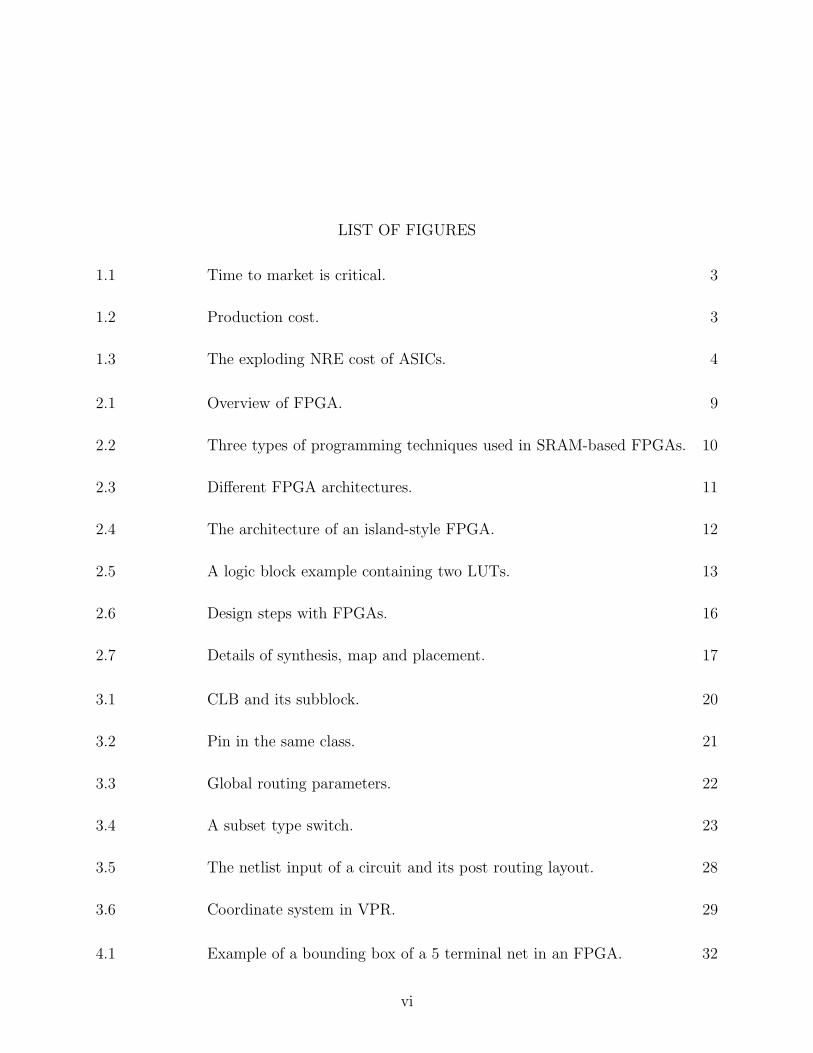
LIST OF FIGURES
1.1 Time to market is critical. 3
1.2 Production cost. 3
1.3 The exploding NRE cost of ASICs. 4
2.1 Overview of FPGA. 9
2.2 Three types of programming techniques used in SRAM-based FPGAs. 10
2.3 Different FPGA architectures. 11
2.4 The architecture of an island-style FPGA. 12
2.5 A logic block example containing two LUTs. 13
2.6 Design steps with FPGAs. 16
2.7 Details of synthesis, map and placement. 17
3.1 CLB and its subblock. 20
3.2 Pin in the same class. 21
3.3 Global routing parameters. 22
3.4 A subset type switch. 23
3.5 The netlist input of a circuit and its post routing layout. 28
3.6 Coordinate system in VPR. 29
4.1 Example of a bounding box of a 5 terminal net in an FPGA. 32
vi

4.2 A circuit with three overlapping bounding boxes: a) Placement may
result in a congested routing. b) Placement leads to a balanced routing.
My goal is to achieve (b). 33
4.3 Ours (congestion driven) vs. VPR. 38
5.1 Generic timing analysis graph. 41
5.2 Timing analysis in VPR. 44
5.3 Data structures of timing in VPR. 45
5.4 A circuit with three nets: my goal is to achieve (c). 50
5.5 Ours (congestion and timing driven) vs. VPR. 54
6.1 Recompute only the costs of affected nets. 56
6.2 Incremental computation of the U array. 58
6.3 The effect of runtime minimization. 61
6.4 The distribution of unoccupied blocks in the placements of VPR and
my approach. I prefer (b) since it is more balanced and is more liable
to reduce channel width. 64
vii
CHAPTER 1
INTRODUCTION
1.1. Motivation
Field programmable gate arrays (FPGAs) have gained rapid commercial acceptance as
their user-programmability offers fast manufacturing turnaround and low non-recurring en-
gineering (NRE) cost. However, the speed and area efficiency of FPGAs lag behind the
application specific integrated circuits (ASICs) and hence deserve more research efforts for
optimizations. Our motivation is is to improve the performance and reduce the occupied
area of an FPGA by improving the placement algorithm in the process of physical design.
1.1.1. The Surge of FPGAs
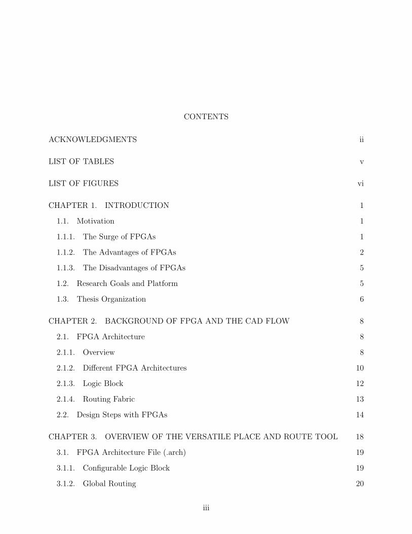
The FPGA industry has grown to multi-billion market today. Table 1.1 shows the revenue
of 4 industry leaders in manufacturing FPGAs.
FPGAs are being widely used in a wide range of applications, ranging from simple glue
logic in a lot of low-cost products, to building up development platforms for many large-scale
designs. Applications of FPGAs include digital signal processing, networking, storage sys-
tems, aerospace and defense systems, ASIC prototyping, medical imaging, computer vision,
Table 1.1: Total revenue of industry players (Unit: million$) [18].
1Q03 2Q03 3Q03 4Q03 1Q04 2Q04
Xilinx 306 313 316 366 403 424
Altera 195 205 209 217 242 268
Lattice 57 56 43 53 59 61
Actel 34 37 38 40 42 44
Total 592 611 606 676 746 797
1

speech recognition, cryptography, bioinformatics, computer hardware emulation, and so on.
Originally, FPGAs began as competitors to complex programmable logic devices (CPLDs)
which are used as glue logic for printed circuit boards (PCBs).
Although prices of FPGA products vary, they are considerably lower than the invest-
ment in a fully customized solution. FPGAs are used in a similar way to customer-specific,
standard cell designs, most commonly used in meeting multiple system design requirements
and/or applications via the use of a single device, with its main advantage being its reconfig-
urability and short development cycles. The FPGA market is forecast to grow from $1,895.0
million in 2005 to $2,756.7 million by 2010 [6].
1.1.2. The Advantages of FPGAs
FPGAs have several advantages such as a shorter time to market, capability of being
re-programed in the field to improve performance or fix bugs, and lower non-recurring engi-
neering costs.
Time to market is crucial to the success of a commercial product. Figure 1.1 shows
the difference of profitability between an early product and a late product. In the industrial
market, designers have a significant incentive to get their products to market quickly to max-
imize revenue and time-in-market. By utilizing the reprogrammabilty of FPGAs, electronic
device vendors can ship full-reconfigurable designs first. After that, vendors may launch
cheaper, less flexible versions of their FPGAs while keep updating the committed designs.
The development of these designs is made on regular FPGAs and then migrated into a fixed
version that more resembles an ASIC.
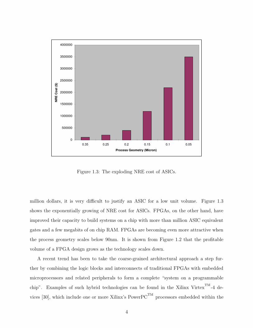
NRE cost refers to the one-time cost of researching, designing, and testing a new product
before producing it in a high unit volume. When budgeting for a project, NRE must be
considered in order to analyze if a new product will be profitable. Even though a company
will pay for NRE on a project only once, NRE can be considerably high and the product
will have to sell well enough to compensate for the initial investment. With the mask costs
approaching a one million dollar price tag, and NRE costs in the neighborhood of another
2

A S I C
F P G A L a t e t o t h e m a r k e t
E n d o f m a r k e t
R e v e n u e
S t a r t o f m a r k e t T i m e
P r o f i t f o r e n t e r i n g i n t o t h e m a r k e t e a r l y
Figure 1.1: Time to market is critical.
T o t a l C o s t
V o l u m e ( K u n i t s )
A S I C . 1 5 u
A S I C . 2 5 u
F P G A . 2 5 u F P G A . 1 5 u
C r o s s o v e r v o l u m e m o v e s h i g h e r
}
Figure 1.2: Production cost.
3
0
500000
1000000
1500000
2000000
2500000
3000000
3500000
4000000
0.35 0.25 0.2 0.15 0.1 0.05 Process Geometry (Micron)
NRE
Cost
($)
Figure 1.3: The exploding NRE cost of ASICs.
million dollars, it is very difficult to justify an ASIC for a low unit volume. Figure 1.3
shows the exponentially growing of NRE cost for ASICs. FPGAs, on the other hand, have
improved their capacity to build systems on a chip with more than million ASIC equivalent
gates and a few megabits of on chip RAM. FPGAs are becoming even more attractive when
the process geometry scales below 90nm. It is shown from Figure 1.2 that the profitable
volume of a FPGA design grows as the technology scales down.
A recent trend has been to take the coarse-grained architectural approach a step fur-
ther by combining the logic blocks and interconnects of traditional FPGAs with embedded
microprocessors and related peripherals to form a complete “system on a programmable
chip”. Examples of such hybrid technologies can be found in the Xilinx VirtexTM
-4 de-
vices [30], which include one or more Xilinx’s PowerPCTM
processors embedded within the
4

FPGA’s logic fabric. The Atmel’s field programmable system level integrated circuits (FP-
SLIC) device is another example, which uses Atmel’s AVR r© processor in combination with
Atmel’s programmable logic architecture [23]. An alternate approach is to use soft pro-
cessor cores that are implemented within the FPGA logic. These cores include the Xilinx
MicroBlazeTM
[28] and PicoBlazeTM
[29], the Altera Nios r© II processors [21], and the open
source LatticeMico8TM
[14], as well as third-party (either commercial or free) processor cores.
many modern FPGAs have the ability to be reprogrammed at “run time”, and this is leading
to the idea of reconfigurable computing or reconfigurable systems – CPUs that reconfigure
themselves to suit the task at hand [59]. Current FPGA tools, however, still can not fully
support this methodology.
1.1.3. The Disadvantages of FPGAs
FPGAs are generally slower than their application-specific integrated circuit (ASIC)
counterparts, can’t handle as complex a design, and draw more power.
The work in [38] presented empirical measurements quantifying the gap between FPGAs
and ASICs. It is observed that for circuits implemented entirely using look-up tables (LUTs)
and flip-fops (logic-only), an FPGA is on average 40 times larger and 3.2 times slower than
a standard cell implementation.
Table 1.2 summarizes the comparison between FPGAs and ASICs.
1.2. Research Goals and Platform
As FPGAs become more and more popular and important, it is more urgent to improve
their performance as well as area efficiency than ever before.
My research goal is to improve timing and reduce routing tracks given an FPGA design.
The complete computer aided design (CAD) flow for synthesizing a FPGA based design
consists of logic synthesis, mapping, placement and routing. My work focuses on placement
algorithms. The objectives of my work are:
(i) To study the current placement algorithms and come up with a novel approach
which is capable of improve the performance of a FPGA design.
5

Table 1.2: Comparisons between FPGAs and ASICs.
FPGA Standard Cell ASIC
NRE Low High
Unit Cost High Low
Risk Low High
Development Span Short Long
Performance Low High
Area Large Small
Capacity Low High
Power High Low
(ii) To research the current placement algorithms and create a novel approach which
is capable of reduce the area of a FPGA design.
(iii) To implement these two algorithms and integrate them into the popular Versatile
Place and Route (VPR) [4] CAD suite.
(iv) To minimize the runtime overhead of these two algorithms so that they can be
integrated in any commercial and practical placement algorithm.
I take VPR as the platform to integrate and evaluate my algorithms because it is consid-
ered as the state-of-the-art academic system to explore placement, routing and architecture
for FPGAs. Also its source code is open.
1.3. Thesis Organization
This thesis is organized as follows. Chapter 2 provides an overview of FPGA architectures
and the CAD flow for logic synthesis. It also reviews previous works on timing and routability
optimization. Chapter 3 describes the framework of VPR, the file format of its input and
output, the core of its placement algorithm. Chapter 4 proposes my congestion driven
optimization. Chapter 5 proposes my timing driven optimization. Chapter 6 describes my
6

approach to minimize runtime. Experimental results are analyzed in chapter 4, 5 and 6.
Chapter 7 draws the conclusion and discuss future research directions.
7
CHAPTER 2
BACKGROUND OF FPGA AND THE CAD FLOW
2.1. FPGA Architecture
2.1.1. Overview
A field programmable gate array (FPGA) is an electrical device containing programmable
logic blocks, I/O pads, and programmable interconnects. The programmable logic blocks
can be programmed to provide the functionality of basic logic gates such as AND, OR,
XOR, NOT or more complex combinational functions such as multiplexers or simple math
functions. The logic blocks also consist of flip flops which are used to build sequential circuits.
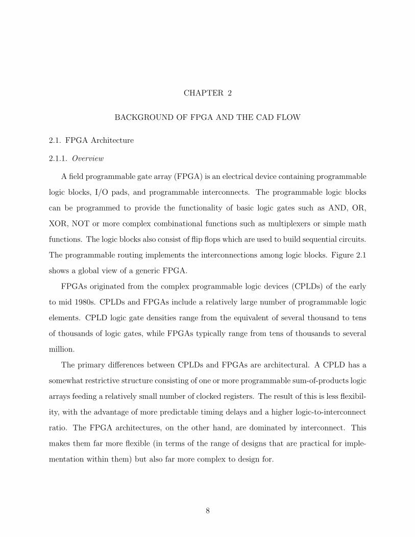
The programmable routing implements the interconnections among logic blocks. Figure 2.1
shows a global view of a generic FPGA.
FPGAs originated from the complex programmable logic devices (CPLDs) of the early
to mid 1980s. CPLDs and FPGAs include a relatively large number of programmable logic
elements. CPLD logic gate densities range from the equivalent of several thousand to tens
of thousands of logic gates, while FPGAs typically range from tens of thousands to several
million.
The primary differences between CPLDs and FPGAs are architectural. A CPLD has a
somewhat restrictive structure consisting of one or more programmable sum-of-products logic
arrays feeding a relatively small number of clocked registers. The result of this is less flexibil-
ity, with the advantage of more predictable timing delays and a higher logic-to-interconnect
ratio. The FPGA architectures, on the other hand, are dominated by interconnect. This
makes them far more flexible (in terms of the range of designs that are practical for imple-
mentation within them) but also far more complex to design for.
8

P r o g r a m m a b l e L o g i c B l o c k P r o g r a m m a b l e
R o u t i n g
P r o g r a m m a b l e I / O
Figure 2.1: Overview of FPGA.
Another notable difference between CPLDs and FPGAs is the presence in most FPGAs
of higher-level embedded functions (such as adders and multipliers) and embedded memories.
A related, important difference is that many modern FPGAs support full or partial in-system
reconfiguration, allowing their designs to be changed “on the fly” either for system upgrades
or for dynamic reconfiguration as a normal part of system operation. Some FPGAs have the
capability of partial re-configuration that lets one portion of the device be re-programmed
while other portions continue running.
There are three different approaches to program an FPGA. The most widely used tech-
nology is using static random access memory (SRAM) cells to control pass transistors, mul-
tiplexers and tri-state buffers in order to configure the programmable routing and logic
blocks. Figure 2.2 shows these SRAM-based switches. Usually, pass transistors use n-
type metal-oxide-semiconductor field effect transistors (nMOS), rather than complementary
transmission gates to get higher speed [10, 34]. Most commercial FPGAs, like most Xilinx
FPGAs [27], the larger Altera devices [20] are SRAM-based. Another popular programming
9

S R A M S R A M
2 S R A M c e l l s
( a ) P a s s t r s n s i s t o r . ( b ) M u l t i p l e x e r . ( c ) T r i - s t a t e b u f f e r .
Figure 2.2: Three types of programming techniques used in SRAM-based FPGAs.
technology is antifuse which consumes less power than SRAM. But it can be programed only
once. Antifuse technology is used in Actel FPGAs [12].
2.1.2. Different FPGA Architectures
There are four widely used architectures for commercial FPGAs. Xilinx [26] and Lu-
cent [55] use island-style, Actel’s FPGAs [13] are row-based, Altera’s FPGAs [22] are hierar-
chical, while Algotronix uses sea-of-gates [31]. Figure 2.3 shows these four architectures. It
should be noted here that new, non-FPGA architectures are beginning to emerge. Software-
configurable microprocessors such as the Stretch r© S5000 [25] adopt a hybrid approach by
providing an array of processor cores and FPGA-like programmable cores on the same chip.
Other devices, such as Mathstar’s Field Programmable Object Array, or FPOATM
[24], pro-
vide arrays of higher-level programmable objects that lie somewhere between an FPGA’s
logic block and a more complex processor.
In this thesis, we focus on the most popular island-style FPGAs. Typically, an island-
style FPGA consists of a two-dimensional array of configurable logic blocks (CLBs), vertical
and horizontal routing channels, and input/output blocks. Figure 2.4 illustrates the top
level architecture of an island-style FPGA. The configurable logic blocks, denoted as CLB
in Figure 2.4, are customizable to implement the logic functions. The connection block [32],
denoted as C in Figure 2.4, connects the CLB pins to the routing channels. A horizontal
10

I n t e r c o n n e c t
L o g i c B l o c k
( a ) I s l a n d - s t y l e . ( b ) R o w - b a s e d .
( c ) S e a o f g a t e s . ( d ) H i e r a r c h i c a l .
L o g i c B l o c k
P L D B l o c k
I n t e r c o n n e c t
Figure 2.3: Different FPGA architectures.
routing channel and a vertical routing channel are connected via a switch block [32] denoted
as S in Figure 2.4. A switch block contains a number of programmable switches which
account for the connections of FPGA routing. Typically, the switches have higher resistance
and capacitance, and hence result in significant delays. The routing channels are segmented
in order to balance the circuit performance and routability. Routing tracks consist of a set
of wires with different lengths where longer wires are desirable for timing-critical nets and
shorter wires are intended for short connections to save routing resources. When routing is
11

C L B C L B
C L B C L B
I / O P a d
S w i t c h B l o c k
C o n n e c t i o n B l o c k
P r o g r a m m a b l e R o u t i n g S w i t c h
P r o g r a m m a b l e C o n n e c t i o n S w i t c h
Figure 2.4: The architecture of an island-style FPGA.
completed for a given circuit, wires, connection blocks and switches will connect the pins of
CLBs and input/output pads together. Each connection consists of a source pin and one or
multiple sink pins and is called a net. As a result, the reduction of routing tracks will lead
to smaller area.
2.1.3. Logic Block
In most FPGAs, the programmable logic blocks consist of clusters of look-up tables
(LUTs) and flip flops along with local routing to connect the LUTs within a cluster. Figure
2.5 shows an example of a typical logic block. For an FPGA using cluster-based logic blocks,
there are many local connections within a cluster. Since this local interconnect is faster than
the general-purpose interconnect among logic blocks, cluster-based logic blocks can improve
FPGA speed. Also, for an FPGA in which every logic block contains multiple LUTs, it will
need fewer logic blocks to implement a circuit. On the other hand, if each logic block in
12

L U T
L U T
L o c a l i n t e r c o - n n e c t
L o g i c b l o c k o u t p u t s L o g i c
b l o c k i n p u t s
Figure 2.5: A logic block example containing two LUTs.
an FPGA contains only a single LUT, it will need much more logic blocks. This reduces
the size of the placement and routing problem considerably. Since placement and routing is
usually the most time-consuming step in mapping a design to an FPGA, cluster-based logic
blocks can significantly reduce design compile time. As FPGAs grow larger, it is important
to keep the compile time from growing too long. Otherwise, the key advantages of FPGAs,
such as rapid prototyping and quick design turns, will be lost.
2.1.4. Routing Fabric
The system of programmable interconnects allows the logic blocks of an FPGA to be
interconnected as needed. These logic blocks and interconnects can be programmed after
the manufacturing process by the customer/designer (hence “field programmable”) so that
the FPGA can perform whatever logical function needed and can be reprogrammed anytime.
Routing can be divided into global routing and detailed routing. The global routing
architecture of an FPGA specifies the relative width of the various wiring channels at different
portions of the chip. For example, some FPGAs have a wider channel width near the center
than near the borders. Some FPGAs use a uniform global routing, i.e., their channels near
the center are as wide as the channels near the edges. In FPGAs, however, all routing
13

resources are prefabricated, so the width of all the routing channels is set by the FPGA
manufacturer.
The detailed routing architecture of an FPGA defines how logic blocks inputs and outputs
can be connected to routing tracks, and how routing tracks can be linked to each other..
Detailed routing architecture is the key element of an FPGA because:
1) Most of an FPGA’s area is devoted to routing resources.
2) Interconnect routing delay assumes the major proportion of the total circuit delay.
3) Interconnect delay does not scale as well as logic delay with process shrinks, so
the fraction of delay due to routing in FPGAs is increasing with each process
generation.
The detailed routing architecture should consider the following issues:
• Which routing wires in the channel adjacent to a logic block input or output can
connect to that logic block pin.
• Where each routing wire starts and how many logic blocks it spans.
• Where routing switches are located and which routing wires they can connect.
• Whether to use a pass transistor or a tri-state buffer for a routing switch.
• The size of the transistors used o build the various switches.
• The metal width and spacing of the various routing wires.
2.2. Design Steps with FPGAs
Implementing a circuit on an FPGA requires programming millions of programmable
switches to their correct states. It is impossible for a developer to specify the state of
each switch manually. In fact, a developer provides a description of a circuit in a hard-
ware description language; i.e., VHSIC Hardware Description Language (VHDL) or Verilog.
Computer-Aided Design (CAD) tools convert this high-level description into a bit-stream
file which is used to configure an FPGA. The entire CAD flow is divided into a set of steps,
as shown in Figure 2.6.
14
The first step is to synthesize the VHDL description into a netlist of basic gates and
clock signals. This step is technology-independent.
Then, the second step optimizes this netlist and maps it to the target FPGA device. This
step is further illustrated in Figure 2.7. First, technology-independent logic optimization is
performed. After that, this netlist of basic gates are mapped onto LUTs and packed into
the logic blocks of a specific FPGA device.
The third step is placement. Placement determines the location of each logic block, i.e.,
it decides the coordinate of each logic block. The optimization objectives include minimizing
wirelength, maximizing circuit speed and so on. This phase is also shown in Figure 2.7.
Once locations of all the logic blocks in a circuit have been fixed, a router is started to
connect all pins in the same net together. A bit-stream used to program all the switches is
produced in this phase. This is the final step in physical design.
A hardware designer may perform a lot of simulations and tests in this flow. Functional
simulation is done on the level of VHDL description. After placement and routing, precise
timing information is acquired. At this point, timing verification can be completed. Finally,
we can download the bit-stream to program the FPGA device and test it in-field.
15

p r o c e s s ( < c l o c k > ) b e g i n i f < c l o c k > ' e v e n t a n d < c l o c k > = ' 1 ' t h e n < o u t p u t > < = < i n p u t > ; e n d i f ; e n d p r o c e s s ;
V H D L s o u r c e c o d e H D L s o u r c e s i m u l a t i o n
N e t l i s t o f g a t e s
S y n t h e s i z e
C L B
N e t l i s t o f b l o c k s
C L B O p t i m i z e a n d M a p
P l a c e a n d R o u t e
C o n f i g u r a b l e L o g i c B l o c k
L U T
1 0 1 1 1 1 1 0 1 1 1 0 0 1 1 1 1 1 1 1 1 1 1 1 1 1 1 0 0 0 0 1 1 0 0 1 1 1 1 1 1 1 1 1 1 1 1 1 1 1 0 0 1 1 1 1 1 1 1 1 1 0 0 0
G e n e r a t e b i t - s t r e a m
B i t - s t r e a m
T i m i n g s i m u l a t i o n
D o w n l o a d
F P G A
F P G A b o a r d
Figure 2.6: Design steps with FPGAs.
16

L U T L U T
L U T
L U T
N e t l i s t o f b a s i c g a t e s
T e c h n o l o g y - i n d e p e n d e n t l o g i c o p t i m i z a t i o n
T e c h n o l o g y m a p t o l o o k - u p t a b l e s ( L U T s )
P u t L U T i n t o l o g i c b l o c k s
L U T
L U T
N e t l i s t o f l o g i c b l o c k s
P l a c e m e n t
L o c a t i o n o f E v e r y B l o c k
Figure 2.7: Details of synthesis, map and placement.
17
CHAPTER 3
OVERVIEW OF THE VERSATILE PLACE AND ROUTE TOOL
The Versatile Place and Route (VPR) suite is a placement and routing tool developed at
the University of Toronto. It is considered as the state-of-the-art academic system to explore
placement, routing and architecture for island-style field programmable gate arrays (FPGAs).
The framework of VPR was setup by Vaughn Betz and Jonathan Rose. Later Alexander
Marquardt added timing driven placement to this suite. VPR is capable of producing a
compact lay out for a given circuit.
To use VPR, we should provide four required parameters in addition to many optional
parameters; it is invoked by typing [3]:
vpr netlist.net architecture.arch placement.p routing.r [-options]
Netlist.net and architecture.arch are input files, while placement.p and routing.r are
output files. Netlist.net describes the netlist of the circuit to be placed and/or routed.
Architecture.arch describes the architecture of the FPGA on which the circuit is to be
implemented. By default, VPR first places the circuit and writes the placement to file
placement.p. Then it routes the circuit according to the placement and outputs the routing
result to file routing.r.
VPR has two basic running modes. In its default mode, VPR places a circuit on an FPGA
and then repeatedly attempts to route it in order to find the minimum number of tracks
on the given FPGA architecture. In the other mode, VPR is invoked with a user-specified
channel width and it reports the circuit can be routed or not [3].
VPR can perform combined global and detailed routing. The key metrics in file routing.r
include critical path delay, channel width and wirelength. These three metrics determine
the overall performance of a post-routing circuit.
18
3.1. FPGA Architecture File (.arch)
Architecture file defines the attributes and capabilities of an FPGA device. It includes
four categories of parameters: configurable logic block (CLB, which corresponds to logic
block in VPR), global routing, detailed routing, and timing. Each line in an architecture file
specify an attribute which is a keyword followed by one or more parameters. In this section,
we will analyze a sample architecture file from VPR website [41]. This FPGA architecture
file is widely used in published research papers related to VPR. We will examine these 4
categories one by one.
3.1.1. Configurable Logic Block
inpin class: 0 bottom
inpin class: 0 left
inpin class: 0 top
inpin class: 0 right
outpin class: 1 bottom right
inpin class: 2 global top #Clock; shouldn’t matter.
subblocks_per_clb 1
subblock_lut_size 4
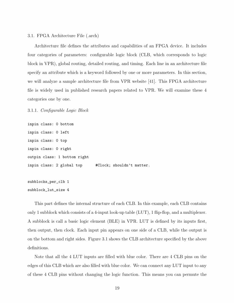
This part defines the internal structure of each CLB. In this example, each CLB contains
only 1 subblock which consists of a 4-input look-up table (LUT), 1 flip-flop, and a multiplexer.
A subblock is call a basic logic element (BLE) in VPR. LUT is defined by its inputs first,
then output, then clock. Each input pin appears on one side of a CLB, while the output is
on the bottom and right sides. Figure 3.1 shows the CLB architecture specified by the above
definitions.
Note that all the 4 LUT inputs are filled with blue color. There are 4 CLB pins on the
edges of this CLB which are also filled with blue color. We can connect any LUT input to any
of these 4 CLB pins without changing the logic function. This means you can permute the
19

4 - i n p u t L U T
D F F
Figure 3.1: CLB and its subblock.
external wires connected to these 4 LUT inputs arbitrarily and still get the desired output.
Figure 5(b) shows an example why this is possible. Assume the external wires are named
A and B. Figure 2(a) is the truth table we want to implement. Figure 2(b) presents one
solution in which A is connected to pin X, and B is connected to pin Y . Since X equals A
and Y equals B, so the LUT table should be the same as the truth table in 2(a). Figure 2(c)
presents another solution in which A is connected to pin Y , and B is connected to pin X.
Since X equals B and Y equals A, so for every entry (x, y) in the LUT table, its value is the
output of entry (y, x) in the truth table in 2(a). As a conclusion, an external wire can be
connected to any pin in the same class without changing the logic function. Only the LUT
table and local connection should be modified. So these 4 CLB pins are logically equivalent
and are declared to be in the same class.
3.1.2. Global Routing
io_rat 2
chan_width_io 1
chan_width_x uniform 1
chan_width_y uniform 1
20

A B O u t 0 0 0 0 1 1 1 0 0 1 1 0
(a) Truth table.
X = A Y = B Z 0 0 0 0 1 1 1 0 0 1 1 0
2 - i n p u t L U T Z
A
B
X
Y
(b) Post-routing layout.
X = B Y = A Z 0 0 0 0 1 0 1 0 1 1 1 0
2 - i n p u t L U T Z
A
B
X
Y
(c) Post-routing layout after
switching A and B.
Figure 3.2: Pin in the same class.
This part defines the global routing attributes of an FPGA. In this example, io rat 2
means there are two input/output (IO) pads per row or column. chan width io 1 means
the width of the channels between the pads and core relative to the widest core channel is
1. That is, the boarder channels are as wide as the channels at the center of the FPGA.
Similarly, we can conclude that all x-directed, y-directed channels, and boarder channels are
of the same width. Figure 3.3 shows the definitions of these terminologies and a sample 4x4
FPGA satisfying these four lines of definition.
21
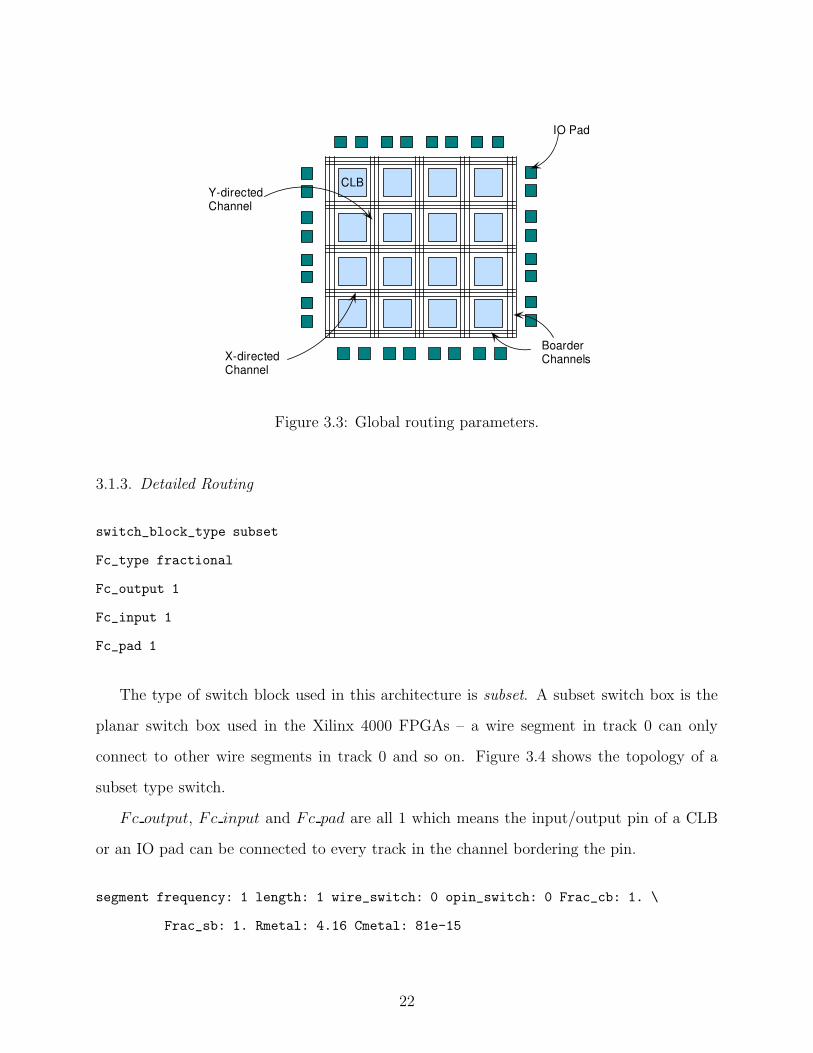
C L B
I O P a d
X - d i r e c t e d C h a n n e l
Y - d i r e c t e d C h a n n e l
B o a r d e r C h a n n e l s
Figure 3.3: Global routing parameters.
3.1.3. Detailed Routing
switch_block_type subset
Fc_type fractional
Fc_output 1
Fc_input 1
Fc_pad 1
The type of switch block used in this architecture is subset. A subset switch box is the
planar switch box used in the Xilinx 4000 FPGAs – a wire segment in track 0 can only
connect to other wire segments in track 0 and so on. Figure 3.4 shows the topology of a
subset type switch.
Fc output, Fc input and Fc pad are all 1 which means the input/output pin of a CLB
or an IO pad can be connected to every track in the channel bordering the pin.
segment frequency: 1 length: 1 wire_switch: 0 opin_switch: 0 Frac_cb: 1. \
Frac_sb: 1. Rmetal: 4.16 Cmetal: 81e-15
22

0 1 2
0 1 2
2
1
0
2
1
0
Figure 3.4: A subset type switch.
switch 0 buffered: yes R: 786.9 Cin: 7.512e-15 Cout: 10.762e-15 Tdel: 456e-12
The segment definition gives the following information:
• The length of all wires in this FPGA is 1.
• The switch type used by other wiring segments to drive this segment is switch 0.
• The resistance per unit length (in terms of logic blocks), in Ohms, is 4.16.
• The capacitance per unit length (in terms of logic blocks), in Farads, is 81e-15.
The only available switch type is switch 0, which uses tri-state buffer. Its resistance is
786 Ohms, its input capacitance is 7.52e-15 F, its input capacitance is 10.762e-15 F, and its
delay is 456e-12 s.
3.1.4. Timing Parameters
C_ipin_cblock 7.512e-15
T_ipin_cblock 1.5e-9
T_ipad 478e-12 # clk_to_Q + 2:1 mux
T_opad 295e-12 # Tsetup
T_sblk_opin_to_sblk_ipin 0 # No local routing
T_clb_ipin_to_sblk_ipin 0 # No local routing
T_sblk_opin_to_clb_opin 0.
23

The most important parameters are C ipin cblock and T ipin cblock. C ipin cblock is
the input capacitance of the buffer isolating a routing track from the connection boxes (mul-
tiplexers) which select the signal to be connected to an logic block input pin. T ipin cblock
is the delay to go from a routing track, through the isolation buffer and a connection block
to a logic input pin [3]. All other timing parameters are related to local connection delay
and are much less than T ipin cblock. They are not as important as T ipin cblock in timing
analysis.
3.2. Circuit Netlist File(.net) Format
The netlist file provides connection information like how many blocks each logic block
connects to and who are these other blocks. There are three different circuit elements in a
netlist file: input pads, output pads, and logic blocks, which are specified using the keywords
.input, .output, and .clb, respectively. The format is shown below:
.input/.output/.clb blockname
pinlist: net_0 net_1 net_2 ...
# Only needed if a clb
subblock: subblock_name pin_num0 pin_num1 ... #BLE0
[subblock: subblock_name pin_num0 pin_num1 ...] #BLE1
...
The first line describes the type and name of this block. The second line begins with
the identifier of the pinlist, and then lists the names of the nets connected to each pin of
the logic block or pad. Input or output pads(.inputs and .outputs) have just one pin, while
logic blocks (.clbs) have as many pins as the architecture file specifies. The first net listed
in the pinlist is connected to pin 0 of a CLB, and so on. If some pin of a CLB is left
unconnected, the corresponding entry in the pinlist should be labeled as open. CLBs (.clbs)
also have to specify the internal connections with subblock lines. Each CLB has at least one
24
subblock line, and may have up to subblocks per clb subblock lines, where subblocks per clb
is specified in the architecture file.
Each subblock contains a K-input LUT(where K is set via the subblock lut size line in
the architecture file) and a flip flop, as shown in Figure 3.1 where K is 4. The subblock line
specifies the name of the subblock, followed by a list of pin names. The first pin, pin num0,
is a CLB pin or a subblock output pin connected to BLE pin 0. So do the remaining pin
names. If a BLE pin is unconnected, the corresponding pin entry is set to the keyword open.
The order of the BLE pins is: subblock lut size LUT input pins, the BLE output, and the
clock input. Each of the subblock LUT input pins can be connected to any of the CLB input
pins, or to the output of any of the subblocks in this CLB. If its is connedted to a CLB input
pin, only the index of this CLB pin is specified. If it is connected to a subblock output,
the entry should be written as ble < subblock number >. For example, to connect to CLB
pin 2, one lists 2 in the appropriate place, while to connect to the output of subblock 1,
one lists ble 1 in the appropriate place. Note that we only need to provide the index of the
subblock because a subblock has only one output pin. Each subblock clock pin can also be
connected to either a CLB input pin or the output of a subblock in the same logic block. If
the subblock clock pin is open the BLE output is the unregistered LUT output; otherwise
the BLE output is registered. The entry corresponding to the subblock output pin specifies
the index of the CLB output pin to which it connects, or open if this subblock output does
not connect to any CLB output pin (It does not mean this output pin is not connected; it
means this subblock output is only used locally, within this CLB).
3.2.1. An Example Circuit
.input i_0
pinlist: i_0
.input i_1
pinlist: i_1
.input i_2
25

pinlist: i_2
.input i_3
pinlist: i_3
.input clk
pinlist: clk
.global clk
.clb clb_0 # Only LUT used.
pinlist: i_0 i_1 i_2 i_3 [0] clk
subblock: sb_zero 0 1 2 3 4 5
.clb clb_1 # Only LUT used.
pinlist: i_4 i_5 i_6 i_3 [1] clk
subblock: sb_zero 0 1 2 3 4 5
.clb clb_2 # Only LUT used.
pinlist: [0] [1] open open o_0 clk
subblock: sb_zero 0 1 open open 4 5
.input i_4
pinlist: i_4
.input i_5
pinlist: i_5
.input i_6
pinlist: i_6
.output out:o_0
pinlist: o_0
This sample circuit (seq s.net) consists of 7 inputs (i 0 to i 6), 3 logic blocks (clb 0 to
clb 2), and an output (o 0). Figure 5(a) shows the corresponding real circuit. The label
inside each logic block is the name of this block. The label on each wire is the name of this
wire. When we invoke VPR using the following commands:
26

vpr seq s.net challenge.arch seq s.p seq s.r
It will produce the placement file named seq s.p and routing file seq s.r. Figure 5(b)
shows the post-routing layout of this circuit which is equivalent to the content of seq s.net.
We can see the channel width of this circuit is 2.
3.3. Placement File
The first line of the placement file shows the netlist (.net) and architecture (.arch) files
used to create this placement. The second line gives the number of rows and columns of the
CLBs used by this placement. All the remaining lines are in the following format [3]:
block name x y subblock number
The block name is the name of this block, as it appears in the input netlist. This block is
placed at row x and column y. The subblock number is meaningful only for IO pads. Because
io rat is set to 2 in the example architecture file shown in Section 3.1, a pad location (x, y)
may contain 2 IO pins. A IO pad may reside in any of the io rat number of possible pad
locations in (x, y), and the location is specified by subblock number. Note that the possible
pad locations at (x, y) are used from 0 to io rat − 1 in order, i.e., if only one pad at (x, y)
is used, the subblock number of the IO pin placed there will be 0. For CLBs, the subblock
number is always 0.
Figure 3.6 shows the coordinate system used by VPR via a nx × ny CLB FPGA (nx =
ny = 2). CLBs all go in the area with x between 1 and nx and y between 1 and ny, inclusive.
All pads either have x equal to 0 or nx + 1 or y equal to 0 or ny + 1.
The placement file seq s.p produced by VPR for the seq s.net input is given below. We
can match it to Figure 5(b). For example, the coordinates for the input pad i 0 is (2,3) in
seq .p, and we can find it top right most in Figure 5(b). For IO pins, we can find i 0 and i 3
are both located at position (2,3).
Netlist file: seq_s.net Architecture file: simple.arch
Array size: 2 x 2 logic blocks
27

i _ 1
i _ 2
i _ 3
i _ 4
i _ 0
i _ 5
i _ 6
c l b _ 0
c l b _ 1
c l b _ 2 o _ 0 o _ 0
[ 0 ]
[ 1 ]
i _ 0
i _ 6
i _ 1
i _ 5
i _ 4
i _ 3
i _ 2
(a) The netlist input.
Block 5 (clb_0) at (2, 2) selected.
i_4
out:o_0
i_0
i_3
clk
i_5
i_6
i_1
i_2
clb_1
clb_2
clb_0
2
3
0
3
1
4
4
2
2
1
0 4
4
1
4
4
(b) The post-routing layout
Figure 3.5: The netlist input of a circuit and its post routing layout.
28

C l b ( 1 , 2 )
C l b ( 2 , 2 )
C l b ( 1 , 1 )
C l b ( 2 , 1 )
C l b ( 2 , 0 )
C l b ( 1 , 0 )
C l b ( 3 , 1 )
C l b ( 3 , 2 )
C l b ( 2 , 3 )
C l b ( 1 , 3 )
C l b ( 0 , 2 )
C l b ( 0 , 1 )
C h a n x ( 1 , 2 )
C h a n x ( 2 , 2 )
C h a n x ( 1 , 0 )
C h a n x ( 2 , 1 )
C h a n x ( 1 , 1 )
C h a n x ( 2 , 0 )
C h a n y ( 0 , 1 )
C h a n y ( 1 , 1 )
C h a n y ( 2 , 1 )
C h a n y ( 2 , 2 )
C h a n y ( 1 , 2 )
C h a n y ( 0 , 2 )
X
Y
0
2
1
3
0 2 1 3
Figure 3.6: Coordinate system in VPR.
#block name x y subblk block number
#---------- -- -- ------ ------------
i_0 2 3 0 #0
i_1 3 2 0 #1
i_2 3 2 1 #2
i_3 2 3 1 #3
clk 3 1 0 #4
clb_0 2 2 0 #5
i_4 1 3 0 #6
i_5 0 2 0 #7
i_6 0 2 1 #8
clb_1 1 2 0 #9
clb_2 2 1 0 #10
out:o_0 2 0 0 #11
29

CHAPTER 4
CONGESTION DRIVEN PLACEMENT
The are three major classes of placers in use today: min-cut (partitioning) based placer [16,
19, 46], analytic placer [1, 2, 36, 45, 50, 52, 51], and simulated annealing based placer [35,
48, 49, 47, 53, 54, 51]. The Versatile Place and Route (VPR) tool uses simulated annealing
method in its placement phase. My proposed algorithms in this thesis are all integrated into
the framework of VPR. I will discuss the details of VPR in the following section.
4.1. Placement in VPR
VPR uses a generic simulated annealing algorithm which is shown in Algorithm 4.1.
The key element in a simulated annealing based algorithm is the cost function. The
following auto-normalizing cost function is used in VPR’s placement algorithm [40]:
(1) ∆C = λ ·∆CT
Previous CT+ (1− λ) ·
∆CW
Previous CW
where CT is the timing cost, CW is the wiring cost, and λ is a user defined constant between 0
and 1 which trades off between timing cost and wiring cost. By default, λ is 0.5. Previous CT
and Previous CW are updated at the beginning of every temperature and used by all moves
at this temperature. The equations to compute CT are given below [40]:
CT =∑
∀i,j∈circuit
CT (i, j)(2)
CT (i, j) = Delay(i, j) · Crit(i, j)Exp(3)
Crit(i, j) = 1−Slack(i, j)
Dmax(4)
30
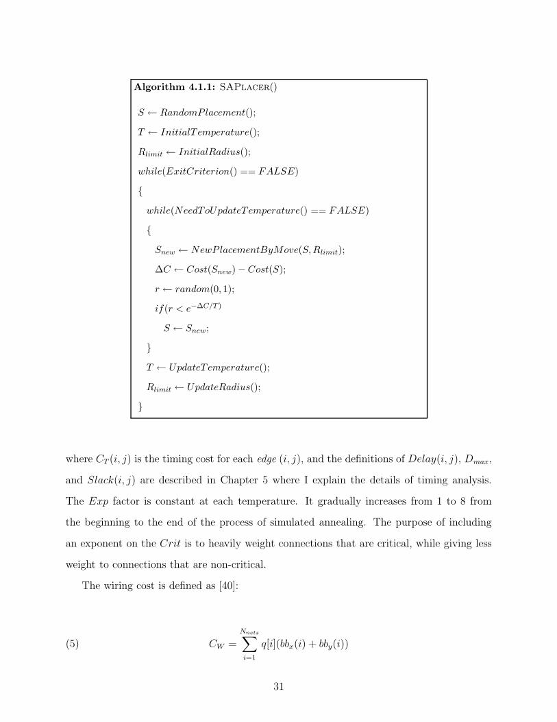
Algorithm 4.1.1: SAPlacer()
S ← RandomPlacement();
T ← InitialT emperature();
Rlimit ← InitialRadius();
while(ExitCriterion() == FALSE)
{
while(NeedToUpdateTemperature() == FALSE)
{
Snew ← NewP lacementByMove(S,Rlimit);
∆C ← Cost(Snew)− Cost(S);
r ← random(0, 1);
if(r < e−∆C/T )
S ← Snew;
}
T ← UpdateTemperature();
Rlimit ← UpdateRadius();
}
where CT (i, j) is the timing cost for each edge (i, j), and the definitions of Delay(i, j), Dmax,
and Slack(i, j) are described in Chapter 5 where I explain the details of timing analysis.
The Exp factor is constant at each temperature. It gradually increases from 1 to 8 from
the beginning to the end of the process of simulated annealing. The purpose of including
an exponent on the Crit is to heavily weight connections that are critical, while giving less
weight to connections that are non-critical.
The wiring cost is defined as [40]:
(5) CW =Nnets∑
i=1
q[i](bbx(i) + bby(i))
31

b b y
b b x
Figure 4.1: Example of a bounding box of a 5 terminal net in an FPGA.
where Nnets is the total number of nets in the circuit. For each net i, bbx(i) is its horizontal
span, and bby(i) is its vertical span. Figure 4.1 shows the bounding box of a 5-terminal net.
The q(i) factor compensates for the fact that the bounding box wire length model usually
underestimates the wiring necessary to connect nets with more than three terminals. The
appropriate values of q(i) are obtained from [9].
4.2. Congestion Metric
From the above analysis we can see that the mutual interactions of different nets are not
taken into account by VPR’s linear congestion method. In this section, I present my method
to overcome this drawback and give a detailed algorithm.
To reduce the routing channel width, a placement algorithm has to pay attention to both
the resource consumed by each net, and the interaction (congestion) among different nets.
The first consideration is to shrink every net as much as possible, since a net expanding
too much needs a lot of wire segments and will increase global congestion. The second
consideration is to disperse different nets as far as possible, because overlapping nets will
add to local congestion. For example, if all nets are restricted to a relatively small fraction
of area on the chip, the routing track demand will probably be very high in this region.
Although configurable logic blocks (CLBs) in other regions may be easily routed with a
32

1 2 2 2
1 1 2 3 3 2
1 2 2 2
1 1 2 3 3 2
(a)
1 1 1 1
1 1 1 1
1 1 1 2 1 1
1 1 1
1 1 1 2 2 1
2 2 2 3 2 1
(b)
Figure 4.2: A circuit with three overlapping bounding boxes: a) Placement may result in a
congested routing. b) Placement leads to a balanced routing. My goal is to achieve (b).
small channel width, the overall channel width is still determined by the channel that uses
the maximum number of tracks if all channels are of the same width.
In my algorithm, I formulated a new wiring cost function. I define a new metric which
evaluates the congestion uniformity of a placement over the entire chip. The final wiring cost
is now computed by multiplying the previous Wiring Cost CW with my congestion coefficient
Congestion (defined in Equation (7)), that is
(6) C ′
W = Congestion · CW
First, I introduce the congestion model used in my algorithm. Assume a circuit consisting
of 3 nets is to be placed. An intermediate placement during the simulated annealing process
is shown in Figure 2(a). The 3 bounding boxes are shown by different rectangles. The
number in each CLB indicates how many bounding boxes are covering this CLB at this
moment. A CLB without a label is not covered by any bounding box (i.e., it is labeled with
33
0). For example, a CLB with label 2 means it is covered by the bounding boxes of two nets.
Since every net will probably need some routing tracks around the CLBs it covers, the regions
covered by more bounding boxes would require more routing resources. In Figure 2(a), the
CLBs with label 3 are very likely to be the bottleneck to reduce channel width. Another
placement shown in Figure 2(b) provides a better solution even though the dimension of
each bounding box remains unchanged. In Figure 2(b), the congestion is dispersed so that
channel width can be reduced.
The following formula is used in my algorithm to compute the congestion coefficient,
Congestion =
(
∑
i,j U2i,j
nx · ny
/(
∑
i,j Ui,j
nx · ny
)
2)k
, 1 ≤ i ≤ nx, 1 ≤ j ≤ ny,(7)
where Ui,j is the number of bounding boxes covering CLBi,j, k is a constant integer for each
circuit (k can be either 2 or 1 and the picking criteria is discussed in Section 5.4), and the
chip consists of nx by ny CLBs.
As we know, for n positive numbers a1, a2, . . . , an, the expression uniform =P
n
i=1a2
i/n
(P
n
i=1ai/n)2
has two properties
(i) uniform ≥ 1. This is true because arithmetic mean is always equal to or greater
than geometric mean.
(ii) A balanced set of ai will give a small uniform. For example, assume n = 4,
consider two set of ai, A1 = {1, 2, 3, 4}, A2 = 2, 2, 3, 3. The sum of all elements in
A1 is 10, the same as of A2. But the uniform of A1 is 1.2 which is greater than
the uniform of A2 (1.04), since the elements in A2 are closer to each other.
So, Congestion is always equal to or greater than 1. In Equation (7), if∑
Ui,j remains
constant, Congestion is determined only by∑
U2i,j. A balanced set of Ui,j will give a small
Congestion. So the value of Congestion indicates how congested the final placement is
expected to be. When it is close to 1, the placement is balanced. If it is much greater than
1, the placement is considered congested.
34

Now let us examine my algorithm on the placements shown in Figure 4.2. Assume k
= 1, apply Equation (7) to Figure 2(a) and Figure 2(b), we can compute the congestions
are Congestiona = 2.04, and Congestionb = 1.446 respectively. As a result, a placement
in Figure 2(b) is favored by my algorithm and CLBs are dispersed more evenly across the
whole chip. The final channel width is very likely be reduced.
Algorithm 4.3.1 is the pseudocode of my proposed algorithm. Function “compBBCost()”
calculates the final wiring cost according to the circuit-specific constant k. Function “get-
BoundingBox()” computes the bounding box for each net and stores its dimension and
location in bb[i]. Function “getNetCost()” obtains the original bounding box cost computed
by VPR using Equation (5), and function “congestionFunc()” calculates the Congestion
factor.
The computation complexity of a single swap is O(n2) in my algorithm. Considering there
are millions of swap in the process of simulated annealing, a trivial implementation will cost
too much runtime. In chapter 6, I provide several techniques to address this problem.
4.3. Experimental Results
I have implemented and integrated my proposed algorithm in the framework of VPR.
The experiments were carried out on an Intel Pentium r©-4 2.8GHz PC with 1GB memory
running the CentOS Linux system. The netlist files of the 20 Microelectronics Center of
North Carolina (MCNC) benchmark circuits and the VPR source code (version 4.3) were
downloaded from [42]. I use gcc 3.4.5 to compile all the source codes.
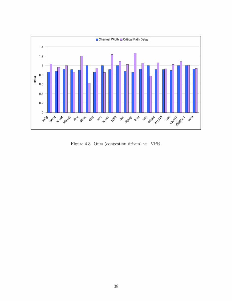
Table 4.1 shows the experimental results of VPR and my congestion approach. Figure 4.3
gives the corresponding chart. All results are normalized to VPR. Compared with VPR, my
algorithm reduces channel width by 7.1% and reduces critical path delay by 0.7%. Although
my approach does not degrade timing in average, it is not preferable that the critical path
delays of several circuits are elongated a lot, such as circuit “alu4”, “apex2”, and “bigkey”.
This problem is addressed in chapter 5.
35

Algorithm 4.3.1: Computing Bounding Box Cost(t)
procedure compBBCost(k)
clearBlkUsage(U)
cost← 0
for n← 0 to num nets
getBoundingBox(bb[n])
for i← bb[n].xMin to bb[n].xMax
for j ← bb[n].yMin to bb[n].yMax
U [i, j]← U [i, j] + 1
cost← cost + getNetCost(n)
congestion← congestionFunc(U, k)
return (cost ∗ congestion)
procedure congestionFunc(U, k)
sum← 0
sos← 0
for i← 1 to nx
for j ← 1 to ny
sos← sos + U [i, j] ∗ U [i, j]
sum← sum + U [i, j]
base← sos ∗ nx ∗ ny/sum2
return (basek)
36

Table 4.1: Experiment results: VPR, VPRb and my algorithm.
Circuit VPR VPRb Mine
CP CW CP Ratio CW Ratio CP Ratio CW Ratio minExp maxExp
tseng 55.62 8 71.56 1.2866 7 0.875 53.65 0.9646 7 0.875 1 2
apex4 93.25 14 131 1.4048 13 0.9286 92.75 0.9946 13 0.9286 1 3
misex3 95.74 12 107.7 1.1249 11 0.9167 82 0.8565 11 0.9167 1 3
dsip 70.79 7 82.14 1.1603 6 0.8571 66.62 0.9411 6 0.8571 1 4
ex1010 195.3 12 206.1 1.0553 10 0.8333 182.6 0.935 11 0.9167 2 4
clma 228.4 14 243.7 1.067 13 0.9286 213.7 0.9356 13 0.9286 3 5
diffeq 101.5 8 93.38 0.92 7 0.875 63.44 0.625 8 1 1 3
spla 203.1 15 181 0.8912 14 0.9333 158.9 0.7824 15 1 1 4
seq 95.72 12 109.7 1.1461 12 1 81.65 0.853 12 1 1 3
elliptic 137.2 12 187.1 1.3637 11 0.9167 126.8 0.9242 11 0.9167 1 4
pdc 193.5 19 211.3 1.092 17 0.8947 198.9 1.028 17 0.8947 2 4
frisc 135 14 176 1.3037 12 0.8571 142.7 1.057 13 0.9286 1 4
bigkey 78.56 7 88.7 1.1291 7 1 99.46 1.266 6 0.8571 1 4
des 121.2 8 114.7 0.9464 8 1 124.2 1.0248 7 0.875 1 4
alu4 82.1 11 121.7 1.4823 10 0.9091 98.93 1.205 10 0.9091 1 3
apex2 90.02 12 134.8 1.4974 11 0.9167 111.8 1.242 11 0.9167 1 3
ex5p 84.06 15 129.4 1.5394 13 0.8667 87.1 1.0362 13 0.8667 1 1
s298 135.7 8 204 1.5033 8 1 148.5 1.0943 8 1 1 4
s38417 103.3 8 156.9 1.5189 7 0.874 112.3 1.087 8 1 2 5
s38584.1 97.92 8 126.7 1.2939 8 1 98.21 1.003 8 1 2 5
Ave 1.2363 0.9192 0.9928 0.9294
37
0
0.2
0.4
0.6
0.8
1
1.2
1.4
ex5p
tse
ng
apex
4
misex3
alu
4 dif
feq
dsip se
q
apex
2 s2
98
des
bigke
y fris
c sp
la
ellipti
c
ex10
10
pdc
s384
17
s385
84.1
clma
Ratio
Channel Width Critical Path Delay
Figure 4.3: Ours (congestion driven) vs. VPR.
38
CHAPTER 5
TIMING DRIVEN PLACEMENT
5.1. Timing Analysis
Timing-driven placement algorithms attempt to place circuit blocks that are on the
critical path into physical locations that are close together. Timing-driven approaches can
minimize the amount of interconnect that the critical signals must traverse. In placement,
timing-driven algorithms can be broadly divided into two classes: path-based and net-based.
Path-based algorithms try to compute the delay of all paths and directly minimize the
longest path delay [17, 33, 51]. This class of techniques are generally based on mathematical
programming and iterative critical path estimation. Path-based algorithms can give an
accurate timing view during the optimization procedure. However, the major drawback is
its high computation complexity due to the exponential number of paths which need to be
simultaneously considered.
Net-based algorithms, on the contrary, do not handle path-based constraints directly [15,
37, 40, 43, 58]. They usually transform timing constraints on paths into either net-length
or net-weight constraints. A popular approach is called net-weighting method. In such
approaches, static timing analysis is applied at intermediate phases and nets are assigned
criticality weights; higher weights are assigned to nets which are more timing critical. After
that moment until the next timing analysis, the criticality of an edge does not change even
its two terminals may be moved.
To perform net-weighting analysis, a directed graph G(V, E) representing the circuit is
constructed. Each wire and each logic block pin becomes a node in the graph, where a pin
comes from a look-up table (LUT), a register, or an input/output (IO) pad. Each switch
becomes a directed edge or a pair of directed edges between two appropriate nodes. Every
39

edge is annotated with a physical delay between the nodes. Figure 5.1 shows a example of
a circuit and its timing analysis graph. A source is the pin of an input pad or a register
output, while a sink is the pin of an output pad or a register input. Each path starts at a
source and ends at a sink. Given a node j, the arrival time, Arr(j), is the time at which the
signal at node j settles to its final value if all primary inputs are stable at time zero. Given
a maximum delay constraint, the required time, Req(j), is the time at which the signal at
node j is required to be stable without elongating the maximum allowed delay.
To determine the arrival time of each node and criticality of each edge, we start from the
source nodes and perform a breadth-first traversal on the graph. The arrival time of each
node j, Arr(j), can be computed, iteratively, from the following equation:
Arr(j) =
0, j ∈ sources
max{Arr(i) + Delay(i, j)}, (i, j) ∈ E(8)
where Delay(i, j) is the delay value of the edge connecting node i and node j. The maximum
arrival time of all nodes in the circuit, Dmax, is calculated as
(9) Dmax = max{Arr(j)}, j ∈ sinks
Once Dmax is available, the required arrival time of each node i, Req(i), can be computed
as follows:
Req(i) =
Dmax, i ∈ sinks
min{Req(j)−Delay(i, j)}, (i, j) ∈ E(10)
Finally, we can determine the slack of an edge (i, j), i.e., the amount of delay that can be
added to (i, j) without causing any path consisting of edge (i, j) become the longest path.
The slack of edge (i, j) is computed as follows:
40

D
CLK
Q
Q
D
CLK
Q
Q
a
b
c
r
d
e
f g
h
i
j
k
l
m
n
o
p
q
(a) Circuit.
a
b
c
r
d
e
f g
h
i
j
k
l
m
n
o
p
q
(b) Timing analysis graph.
Figure 5.1: Generic timing analysis graph.
(11) Slack(i, j) = Req(j)− Arr(i)−Delay(i, j)
Under this framework, the Versatile Place and Route (VPR) suite utilizes a simulated
annealing based method [40]. Kong proposed an efficient all-path counting algorithm called
PATH [37]. PATH assigns weight to each edge based on the number and criticality of paths
41

using this edge. Wang et al. tried to improve timing by using linear programming (LP)
relaxation [58]. This approach captures all topological paths in a linear sized LP and thus
avoids heuristic net weighting. Ren et al. proposed a net weighting algorithm considering
both figure of merit (FOM) and slack sensitivities [43]. Recently, a new technology called
grid-warping was proposed which elastically deform a model of the 2-D chip surface on which
the gates have been roughly placed [61]. Xiu et al. designed a timing-driven grid-warping
placer [62] using an accurate slack sensitivity analysis method [44] for net weighting.
Differing from the above approaches which work in placement phase, Lin et al. proposed
an algorithm named SMAC recently optimizing timing during mapping and packing [39].
But this algorithm introduces a high area overhead.
Generally, to simultaneously optimize multiple metrics during placement is very challeng-
ing. Most research works can only improve one perspective of the circuit with degradation
on other factors. For example, the work in [37] and [58] can improve timing, but the former
needs more wire length and the latter results in more channel width. However, some research
works improve multiple metrics of the design simultaneously. In [7], Chang et al. proposed
an architecture-driven metric which pays attention to the number of segments traveled by a
net and congestion on segments of specific lengths. In [57], Viswanathan et al. proposed a
fast, analytical placer, FastPlace 2.0, which reduces wirelength and run time for stand cell
placement.
Note that VPR, t-RPack, cMap and Brenner’s work all fall into this category. My
proposed algorithm also increases circuit speed as well as reduces channel width.
5.2. Timing Analysis Graph
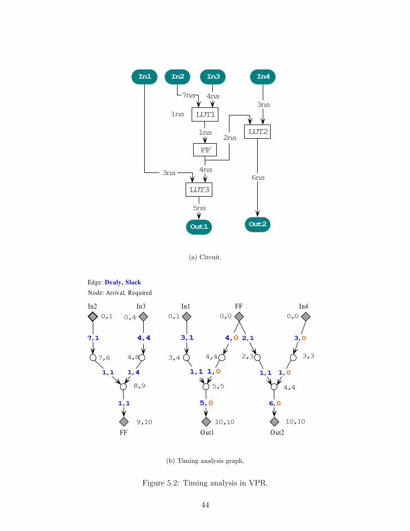
Timing analysis graph is the core of every timing-driven placement algorithm. Figure
5.2 shows how VPR constructs a timing analysis graph from a circuit. Figure 2(a) shows
a circuit which consists of 4 inputs, 3 LUTs, 1 flip flop and 2 outputs. The delay of each
wire is annotated on it. We assume the local delay within each LUT is 1ns, that is, it takes
a signal 1ns from it reaches the input pin to get out of the LUT. Figure 2(b) presents the
42

corresponding graph for timing analysis. Note that register input pins are not joined to
register output pins – register outputs have no edges incident to them, and register inputs
have no edges leaving them. The reason is when a clock signal arrives, the output of a
register is refreshed and begins to excite all its successors. As long as the effected successive
signals arrive at the the input of a register or an output pad, they will not interfere with
signals in the next clock cycle. Utilizing this method we can break all possible circuits into
acyclic directed graph. It can be seen that the timing analysis graph is a forest instead of
a tree in general. In Figure 2(b), each edge is annotated with a pair of (Delay, Slack).
The value of Slack is computed from Equation (11). Each node is annotated with a pair of
(arrival, required) which are computed from Equation (8) and Equation (10) respectively.
Some edge’s slack value is 0 and is labeled using a red color. An edge with zero slack is on
the critical path. That means any delay on such an edge will elongate the minimum period
needed for the last signal to become stable at the output. We can see in this example there
are 6 critical edges and 2 critical paths. In timing analysis, a critical edge or path is paid
more attention to than others because they determine the speed of a circuit. By intuition
we know a balanced forest is more liable to produce a smaller critical path delay.
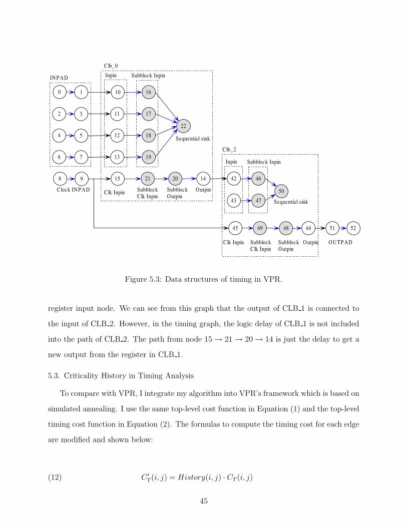
Figure 5.3 gives a more detailed visualization of the timing analysis graph. It shows
a typical run time data structure when VPR is performing timing-driven placement. The
corresponding input circuit is Figure 5(a) in Chapter 4. There are two nodes for each pin
of an input pad. First node is the input node to the pad – nothing comes into this. Second
node is the output node of the pad, that has edges to CLB input pins. In addition, global
clocks from pads arrive at T = 0. The earliest any clock can arrive at any flip flop is T =
0, and the fastest global clock from a pad should have zero delay on its edges so it does get
to the flip flop clock pin at T = 0. Similarly, every pin of an output pad corresponds to
two nodes in the graph. When building the subblock input pins, if the subblock is used in
sequential mode (i.e. is clocked), two clock pin nodes are created. First node is the clock
input pin; it feeds the sequential output. The other node is the ”sequential sink”, i.e., the
43
I n 3 I n 4
4 n s 3 n s
1 n s L U T 1
O u t 1
4 n s
L U T 3
2 n s
I n 2
7 n s
L U T 2
5 n s
F F
O u t 2
6 n s
I n 1
3 n s
1 n s
(a) Circuit.
7 , 1
1 , 1 1 , 4
3 , 0 2 , 1
1 , 0 1 , 1
6 , 0 1 , 1
7 , 8 3 , 4
8 , 9
1 0 , 1 0
4 , 4
9 , 1 0
0 , 1 0 , 1 0 , 0
N o d e : A r r i v a l , R e q u i r e d E d g e : D e a l y , S l a c k
I n 4 F F I n 3 I n 2
4 , 4
F F
I n 1
3 , 1 4 , 0
1 , 1 1 , 0
5 , 0
O u t 1 O u t 2
4 , 8 4 , 4
5 , 5
1 0 , 1 0
2 , 3 3 , 3
0 , 4 0 , 0
(b) Timing analysis graph.
Figure 5.2: Timing analysis in VPR.
44
S u b b l o c k I n p i n
0 1
2 3
4 5
6 7
8 9
1 0
1 1
1 2
1 3
1 5
1 6
1 7
1 8
1 9
1 4 4 2 2 1
2 2
2 0 4 6
4 3 4 7
4 4 5 1 4 5 4 9
5 0
4 8 5 2
I N P A D
C l o c k I N P A D
C l b _ 0
C l k I n p i n
I n p i n
O u t p i n S u b b l o c k C l k I n p i n
S u b b l o c k O u t p i n
S e q u e n t i a l s i n k
C l k I n p i n O u t p i n S u b b l o c k C l k I n p i n
S u b b l o c k O u t p i n
O U T P A D
S e q u e n t i a l s i n k
S u b b l o c k I n p i n I n p i n
C l b _ 2
Figure 5.3: Data structures of timing in VPR.
register input node. We can see from this graph that the output of CLB 1 is connected to
the input of CLB 2. However, in the timing graph, the logic delay of CLB 1 is not included
into the path of CLB 2. The path from node 15→ 21→ 20→ 14 is just the delay to get a
new output from the register in CLB 1.
5.3. Criticality History in Timing Analysis
To compare with VPR, I integrate my algorithm into VPR’s framework which is based on
simulated annealing. I use the same top-level cost function in Equation (1) and the top-level
timing cost function in Equation (2). The formulas to compute the timing cost for each edge
are modified and shown below:
C ′
T (i, j) = History(i, j) · CT (i, j)(12)
45
where CT (i, j) comes from Equation (3). The new element in Equation (12) is the
History(i, j) factor, which will be explained below in details.
Since the cost to compute the criticality for each edge from a timing-analysis graph is
very high, general timing analysis algorithms can only afford executing this computation
once every temperature. As a result, the accuracy becomes less reliable because there are
tens of thousands of moves per temperature. The delay of an edge may differ a lot from the
original value when the graph was annotated. This is the problem I have addressed in my
algorithm.
My approach increases the accuracy without paying much run time penalty. I observed
the following two facts: 1) The criticality of a given edge varies in multiple rounds of timing
analysis. 2) Some edges are almost always among the most critical edges. In other words,
no matter how the configurable logic blocks (CLBs) and IO pads are placed, the criticality
value of some edges are always high.
My approach takes advantage of the second phenomenon and thus improves circuit
speed. In my algorithm, the criticality value of an edge (i, j) is accumulated into a vari-
able CritStat(i, j) every time it is computed. An edge which is often timing-critical will get
a high accumulation value. I then favor those historically timing-critical edges by using this
statistical data. The accumulation value CritStat(i, j) is computed as:
(13) CritStat(i, j) = (
Nt∑
k=1
Critk(i, j) · αNt−k)/(
Nt∑
k=1
αNt−k)
where Nt is the number of different temperatures since the beginning of the simulated an-
nealing process. Critk(i, j) is the value of Crit(i, j) at the kth temperature. α is a decay
constant and I use 0.96 in my algorithm. As we can see, CritStat(i, j) is a weighted mean
over all Crit(i, j) in the history. The weight for the kth Crit(i, j) is αNt−k. In other words,
the criticalities at different temperatures are not treated equally. I assign more weight to a
recent criticality value since it is more accurate and reliable. Considering the net-weighting
method used in VPR, after constructing the timing graph G(V, E) at the beginning of every
46

temperature, VPR uses only G to compute CT (i, j). My approach considers not only the
current G, but also the previous G′s in computing C ′T (i, j). Utilizing the entire criticality
history, I avoid the randomness encountered by general timing-analysis methods and hence
increase the accuracy.
The History(i, j) factor, used in Equation (12), is computed from CritStat(i, j) as de-
fined in Equation (13). In order to compute History(i, j), I divide the simulated annealing
process into two phases. As long as the radius to swap two blocks is greater than 1.0, it is
in Phase0, otherwise it is in Phase1.
In Phase0, I update CritStat(i, j) at every temperature, but do not use it to com-
pute History(i, j) because the statistical data are not enough as guidance. So, in Phase0,
History(i, j) is always 1.0 and does not affect the timing cost.
In Phase1, I keep updating CritStat(i, j) and use it to compute History(i, j). Let
NC denote the number of edges that are considered most timing-critical in history. At the
beginning of each temperature, I recompute CritStat(i, j) for every edge and select NC edges
with the highest CritStat values. I call these edges potential critical edges (PCE). Also I
set the variable CritThres to the (NC +1)th highest CritStat. Then I compute History(i, j)
by the following formula:
(14) History(i, j) = max(CritStat(i, j)− CritThres + 1, 1)
It can be seen that for the NC number of edges with the highest criticalities in the
history, their History(i, j) values are greater than 1. Assume that there are Nedges edges in
the timing-analysis graph, then the values of History(i, j) for all the remaining (Nedges−NC)
number of edges are 1. I only favor the first NC edges in the criticality history. And the
more critical an edge is in the history, the more it is favored.
In my algorithm, NC is an integer constant for a particular circuit. Intuitively, the value
of NC should be as small as possible. Since only the edges with the potentials to appear in
47

the post-routing longest path should be favored. On the other hand, it should not be too
small, otherwise the probability of missing a final critical edge is high. I use the following
formula to compute NC :
(15) NC = max(√
1.54 ·Nedges · (1− 4 · empty rate), 64)
where empty rate is the percentage of unoccupied CLBs on the chip. First, NC grows
as the total number of edges increases. This is natural because I need to consider more
edges as the circuit becomes larger and more complex. Second, NC increases as empty rate
decreases. The reason is that when empty rate is low, the layout is compact and relatively
more congested. In this case, favoring a critical edge may easily force other non-critical edges
to take detours and become critical. So I need to consider more edges simultaneously. The
value of 1.54 and 4 in Equation (15) are obtained through experiments. In addition, I will
track at least 64 potential critical edges, so I put a lower bound of 64 in this equation.
Two techniques are used to further improve the performance of my algorithm. First, I
observed that my algorithm works better in a less congested environment because it is easier
to favor the PCEs without influencing other edges. To do so, I set λ = 0.3 in Equation (1)
when empty rate < 2% to alleviate congestion. Otherwise, λ is set to the default value of
0.5. The value of λ for each circuit is shown in Table 5.2. From the above analysis, I shall
expect the congestion-driven part of my algorithm to benefit the timing-driven part, because
it provides a less congested environment. This explains why my algorithm improves both
timing and congestion because these two optimizations favor each other.
The other technique used is to get more criticality data. My algorithm is based on
the statistics of criticalities and works better when it gathers more history information.
Therefore, I need to modify the annealing schedule. The goal is to keep the total number of
moves about the same as in VPR but increase the number of different temperatures. The
number of moves evaluated at each temperature is (Nblocks)1.33 in my algorithm, about 1/10
as in VPR. And the number of different temperature is about 10 times as in VPR. A new
48

Table 5.1: Temperature Update Schedule
Fraction of moves accepted (Raccept) γ
Raccept > 0.96 0.65
0.8 < Raccept ≤ 0.96 0.976
0.15 < Raccept ≤ 0.8 0.996
Raccept ≤ 0.15 0.93
temperature is computed as Tnew = γ Told, where γ depends on the fraction of attempted
moves that were accepted (Raccept) at Told, as shown in Table 5.1.
5.4. Refined Congestion Metric
First, let us reexamine my algorithm using Figure 5.4. Figure 4(a) shows a placement
for a circuit consisting of three nets. I assume the target FPGA chip consists of 6x6 CLBs.
Figure 4(b) shows the corresponding U array for this placement. The number in each CLB
indicates how many bounding boxes are covering this CLB at this moment. A CLB without
a label is not covered by any bounding box. For example, the value of U3,3 is 3 since it is
inside the bounding box of all the 3 nets, and the value of U1,1 is assigned 0 because it is
not inside any bounding box. In Figure 4(b), only the CLBs used by the circuit are shaded.
Note that an unused CLB can also be covered by some bounding boxes, like CLB5,2.
In FPGA based designs, we can hardly utilize all CLBs and hence those unused CLBs
are generally neglected and wasted. However, they are valuable since they do not consume
any routing resources. Instead, routing tracks around them can be used by other CLBs.
So, unused CLBs should be placed in the most congested regions as long as this placement
does not degrade other metrics too much. Figure 4(c) is a placement after swapping CLB4,2
and CLB5,2 (striped) in Figure4(a). This swap will probably reduce channel width since
the traffic at the center of the chip is reduced. But this swap will not be favored by my
algorithm defined in Equation (7) since these two placements have the same U array as shown
in Figure 4(b), and thus the same value of Congestion. Similarly, it can not be favored by
49

X 1 5 2 3 4 6
Y
1
2
3
4
5
6
n e t 1
n e t 2
n e t 3
(a) Placement with poor routability.
1 1 1 1
1 1 1 1
1 1 1 2 1 2
1 2 1 3 1 3
1 1 2 1 2
1 1 2 1 2
X 1 5 2 3 4 6
Y
1
2
3
4
5
6
n e t 2
n e t 1
n e t 3
(b) Congestion map.
��
X 1 5 2 3 4 6
Y
1
2
3
4
5
6
n e t 1
n e t 2
n e t 3
(c) Placement with good routability.
Figure 5.4: A circuit with three nets: my goal is to achieve (c).
VPR’s wiring cost function either, because the dimension and position of all the three nets
do not change at all.
My approach addresses this problem by considering unoccupied CLBs and IO pads. The
objective is to make the factor Congestion smaller when more unoccupied CLBs are placed
in congested regions. To quantify the alleviation of congestion brought by an unused block,
50
I define a factor Satx,y indicating the effective percentage of Ux,y. That is, for CLBx,y,
(1 − Satx,y) fraction of Ux,y is alleviated. The following formulas show how to compute
EUx,y, the effective percentage of Ux,y,
EUx,y = Ux,y · Satx,y(16)
Satx,y =
1−Nun · allev, CLBx,y is used
1−Nun · allev/2, otherwise(17)
allev = min(β/empty rate, 6%)(18)
where Nun is the number of unused CLBs or IO pads adjacent to CLBx,y. The maximum
value of Nun can be 4. I need consider the number of empty blocks adjacent to each CLB.
Preferably, I would like to compute Satx,y in such a way that the more empty blocks CLBx,y
is adjacent to, the smaller Satx,y becomes. This is taken into account by introducing Nun in
Equation (17). On the other hand, I want to avoid placing a large number of unused blocks
in the same region in order to reduce congestion.This is why I use allev/2 in Equation (17)
when CLBx,y is not occupied. Several facts can be inferred from this set of equations:
1) If CLBx,y is not adjacent to any unused blocks, its Nun is 0 and Satx,y is 1, so
EUx,y equals Ux,y.
2) If CLBx,y is adjacent to some unused block(s), its EUx,y is less than Ux,y.
3) When adjacent to the same Nun number of empty blocks, Ux,y of an unused CLB,
CLBx,y, is not alleviated as much as a used CLB.
It is clear that the value of allev is very important. If it is too small, the effect will
be negligible. If it is too large, the locations of empty blocks will become a primary factor
when computing the Congestion factor in Equation (19). As a result, all empty blocks will
be converged to the center of the chip, which is not favorable. Based on my experiments,
our algorithm performs well when the allev factor is smaller than 6%. In general, I want to
restrict the value of allev between 2% to 6%. Since most circuits have an empty rate also
51

between 2% to 6%, the value of β is set to 2% · 6% = 0.12% in my approach. Also I put
an upper bound of 6% to allev in Equation (18) in case some circuit has an extremely small
empty rate.
I use the following modified congestion function in my approach:
Congestion =
(
∑
x,y EU2x,y
nx · ny
/(
∑
x,y Ux,y
nx · ny
)
2)k
, 1 ≤ x ≤ nx, 1 ≤ y ≤ ny(19)
Note, I only use EU in the numerator. When the U array remains constant, the de-
nominator remains constant. And the numerator will be minimized if unoccupied blocks are
moved to the neighborhood of CLBs with highest Ux,y values. So, utilizing the approach
above has the effect to move unused CLBs to congested regions.
Based on the discussion above, I can draw two reasonable conclusions.
(i) If there are plenty of empty blocks, the routability is good by nature. So, I turn
off this optimization when empty rate is greater than 25%.
(ii) On the other hand, if all empty blocks are IO pads instead of CLBs, this algorithm
will not work well since IO pads can only be moved along the borders. According
to VPR’s layout method, a small value of empty rate means there are a lot of
unused IO pads but very few empty CLBs. So, I turn off this optimization when
empty rate is less than 0.6%.
I also use empty rate to decide the value of k in Equation (19). I set k to 2 for a circuit
with a low empty rate (< 4%) and set to 1 otherwise. The reason is I need to assign more
weight to the Congestion factor if the circuit is congested by nature.
VPR provides graphic visualization of placement and routing results which helps a re-
searcher understand how well or how poorly an algorithm does. We can get a global view
of my placement algorithm by looking at Figure 6.4.2. The details of this figure will be
explained in Chapter 6.
52

Table 5.2: Experiment results: VPR vs. mine.
Circuit Critical Path Delay Routing Tracks Parameters Statistics runtime
name empty rate Nedges VPR mine ratio VPR mine ratio k λ NC/Nedges hit ratio
s298 0.258% 6951 148.2 136.9 0.924 8 8 1 2 0.3 1.5% 100% 1.76
ex1010 0.562% 16078 174.5 176.0 1.009 12 11 0.917 2 0.3 1.0% 25.0% 1.69
seq 0.794% 6193 109.5 101.6 0.928 12 12 1 2 0.3 1.5% 71.4% 2.11
spla 0.833% 13808 165.6 167.3 1.01 15 16 1.06 2 0.3 1.0% 33.3% 2.41
clma 0.957% 30462 206.5 187.2 0.907 15 13 0.867 2 0.3 0.7% 40.0% 2.41
pdc 1.060% 17193 194.8 206.7 1.061 18 18 1 2 0.3 0.9% 40.0% 2.40
frisc 1.222% 12772 132.5 133.8 1.01 14 13 0.929 2 0.3 1.0% 100% 2.33
diffeq 1.578% 5296 63.72 60.45 0.949 9 8 0.889 2 0.3 1.6% 100% 2.11
s38584.1 1.738% 20840 112.3 82.95 0.739 9 8 0.899 2 0.3 0.8% 100% 2.25
ex5p 2.296% 4002 77.21 79.75 1.033 15 14 0.933 2 0.5 1.8% 0% 2.03
s38417 2.362% 21344 103.3 83.00 0.803 9 9 1 2 0.5 0.8% 63.6% 3.14
apex4 2.623% 4479 103.1 75.43 0.732 14 14 1 2 0.5 1.7% 14.3% 2.56
apex2 2.996% 6692 100.8 94.60 0.939 12 12 1 2 0.5 1.3% 100% 2.76
elliptic 3.144% 12634 136.6 126.0 0.922 13 11 0.846 2 0.5 1.0% 0% 2.84
misex3 3.255% 4968 82.57 88.58 1.073 12 12 1 2 0.5 1.5% 28.6% 2.66
tseng 3.857% 3760 57.96 53.24 0.918 8 7 0.875 2 0.5 1.7% 0% 2.31
alu4 4.875% 5408 90.58 94.76 1.046 11 10 0.909 1 0.5 1.3% 25.0% 3.06
bigkey 41.46% 6313 72.56 55.27 0.762 7 7 1 1 0.5 1.0% 66.7% 1.63
dsip 53.02% 5645 74.37 51.69 0.695 8 7 0.875 1 0.5 1.1% 100% 1.54
des 59.91% 6110 87.21 80.79 0.926 8 8 1 1 0.5 1.0% 0% 1.72
Ave 0.919 0.950 1.2% 50.4% 2.29
53

0
0.2
0.4
0.6
0.8
1
1.2
s298
ex10
10
seq
spla
clma pd
c fris
c dif
feq
s385
84.1
ex5p
s384
17
apex
4
apex
2
misex3
tse
ng
alu4
bigke
y ds
ip des
ellipti
c
Ratio
Channel Width Critical path Delay
Figure 5.5: Ours (congestion and timing driven) vs. VPR.
5.5. Experimental Results
The experimental environment is the same as the one used in Chapter 4. As I made a
lot of modifications to VPR, those single-precision floating-point variables cannot provide
enough precision any more. So I changed all “float” variables to “double”. To compare with
VPR fairly, I also changed all “float” variables in VPR’s source code to “double”. Note, this
is the only change that I made to the VPR’s source code.
Table 5.5 shows the experimental results of VPR and my congestion approach. Figure
5.5 gives the corresponding chart. All results are normalized to VPR. Compared with VPR,
my algorithm reduces channel width by 5.3% and reduces critical path delay by 11.8%.
54

CHAPTER 6
RUNTIME MINIMIZATION
Recently, as circuit designs become more and more complex, commercial field pro-
grammable gate array (FPGA) manufactures keep releasing larger and more powerful FPGA
devices. As a direct result, the runtime issue has drawn more attentions than ever before.
Runtime is an important metric for a placement algorithm, especially for a simulated an-
nealing based one. This is because although a simulated annealing based approach can
generally produce a high quality placement, its runtime is usually prohibitively longer than
an analytical placement algorithm.
To overcome this drawback, many methods have been proposed. One is to enable sim-
ulated annealing only when the temperature is low, like Frontier, a system developed by
Tessier to achieve highly routable and high-performance layouts quickly [56]. Another is
to utilize hardware to assist simulated annealing, like the systolic structure proposed by
Wrighton et al. in [60].
In this chapter, I will present three different runtime minimization measures. The first
one is proposed by Betz in [5], the second and third are proposed by us.
6.1. Recompute Only the Costs of Affected Nets
The runtime of a placement algorithm is mainly dependent on its computation complex-
ity. However, if I can find a clever incremental computation method, the needed runtime
can be reduced significantly. For example, for an algorithm whose complexity is O(n), if I
can find an incremental method which can be always completed in a constant time, the final
complexity will be O(1).
The most important runtime optimization techniques comes from the observation that
only a small number of nets will be affected in a swap. VPR uses simulated annealing method
55

B
A . . . . . .
. . . . . .
. . . . . .
. . . . . .
Figure 6.1: Recompute only the costs of affected nets.
to place a circuit. At each step, two random configurable logic blocks (CLBs) are chosen
and their locations are swapped. After that I compute the new cost and compare it with the
old cost to determine whether to accept this swap or not. The simplest method to compute
a new cost is to compute every thing from scratch. But this method is infeasible because
there are thousands of nets in a circuit which will make the computation time intolerably
long. However, if we take a close look at Equation (2) and Equation (5), it is clear that the
timing cost and wiring cost can be decoupled into every net. So in each swap, I only need to
recompute the cost for a few affected nets. This is illustrated in Figure 6.1. In Figure 6.1,
two CLBs, A and B, are chosen to be swapped. A is connected to 4 nets while B is connected
to 3 nets. Although there are much more nets in this circuit, I only need to recompute the
new cost for these 7 nets.
56
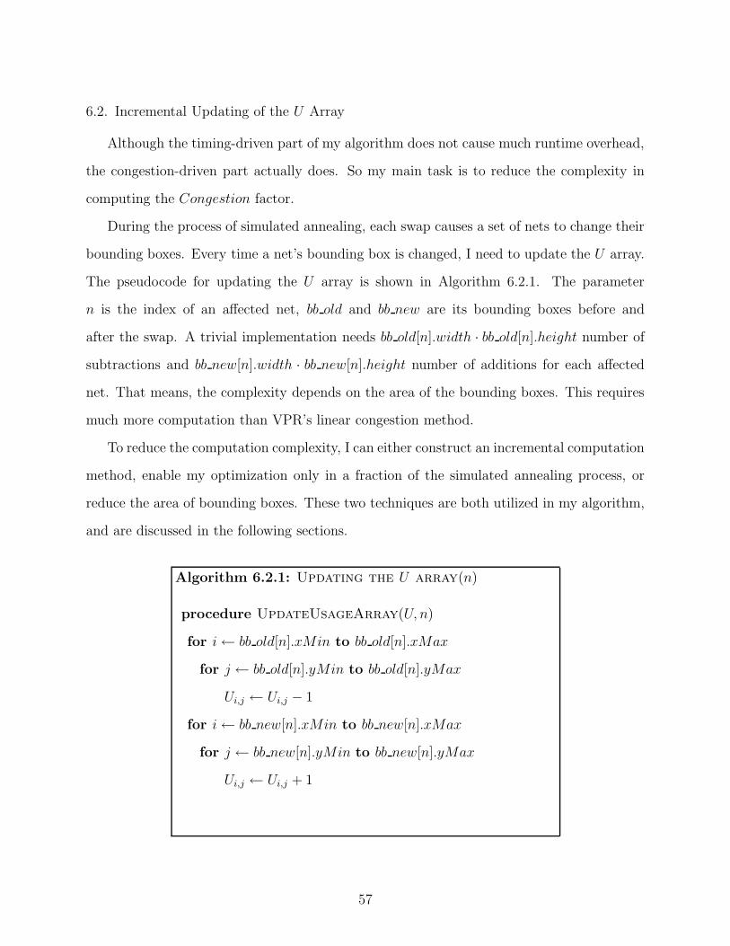
6.2. Incremental Updating of the U Array
Although the timing-driven part of my algorithm does not cause much runtime overhead,
the congestion-driven part actually does. So my main task is to reduce the complexity in
computing the Congestion factor.
During the process of simulated annealing, each swap causes a set of nets to change their
bounding boxes. Every time a net’s bounding box is changed, I need to update the U array.
The pseudocode for updating the U array is shown in Algorithm 6.2.1. The parameter
n is the index of an affected net, bb old and bb new are its bounding boxes before and
after the swap. A trivial implementation needs bb old[n].width · bb old[n].height number of
subtractions and bb new[n].width · bb new[n].height number of additions for each affected
net. That means, the complexity depends on the area of the bounding boxes. This requires
much more computation than VPR’s linear congestion method.
To reduce the computation complexity, I can either construct an incremental computation
method, enable my optimization only in a fraction of the simulated annealing process, or
reduce the area of bounding boxes. These two techniques are both utilized in my algorithm,
and are discussed in the following sections.
Algorithm 6.2.1: Updating the U array(n)
procedure UpdateUsageArray(U, n)
for i← bb old[n].xMin to bb old[n].xMax
for j ← bb old[n].yMin to bb old[n].yMax
Ui,j ← Ui,j − 1
for i← bb new[n].xMin to bb new[n].xMax
for j ← bb new[n].yMin to bb new[n].yMax
Ui,j ← Ui,j + 1
57

b b _ o l d [ n ]
b b _ n e w [ n ]
Figure 6.2: Incremental computation of the U array.
First, not all elements inside the bb old[n] or bb new[n] should be updated. Figure 6.2
shows the bounding boxes of a net before and after a swap. Actually, only the shaded
elements need to be updated. The overlapped elements do not change at all. In general,
bb old[n] intersects bb new[n]. This is because a net connects at least two blocks and a swap
can at most change the positions of two blocks. So I can always use the above optimization
to reduce runtime. The overlap region can be computed using the following assignments:
overlap.xmin = max(bb_old[n].xmin, bb_new[n].min);
overlap.xmax = min(bb_old[n].xmax, bb_new[n].xmax);
overlap.ymin = max(bb_old[n].ymin, bb_new[n].ymin);
overlap.ymax = min(bb_old[n].ymax, bb_new[n].ymax);
6.3. Trade-off Between Performance and Runtime
Another technique is to enable the congestion optimization only after the swap radius is
reduced to 1.0. This technique reduces the runtime considerably in that:
1) The length of period when the swap radius equals 1.0 is only about 1/3 of the entire
placement period. So about 2/3 computation will be reduced.
2) After the swap radius reaches 1.0, the simulated annealing process is about to
end. At this moment, the dimension of almost every net (the area of every net’s
58

bounding box) has shrunk a lot. As the complexity of updating the U array is
directly related to the area of a net’s bounding box, this optimization technique is
able to reduce computation complexity effectively.
According to my experiments, among the above 2 factors, factor 2 is more important than
factor 1. In fact, I think it is factor 2 that makes the runtime ratio between my algorithm
and VPR become a constant. That means, the ratio does not grow as the size of the FPGA
device grows, which will be analyzed in the following section.
6.4. Experimental Results and Analysis
6.4.1. Comparison with VPR
The experimental environment is the same as used in Chapter 5. Table 5.2 shows the re-
sults of VPR and my algorithm. The circuits are sorted in the ascending order of empty rate.
Compared with VPR, my algorithm reduces the critical path delay by 8.1% and the channel
width by 5.0% at the same time. The “NC/Nedges” column shows the fraction of edges that
are favored in my timing cost computation. Let PCElast be the set of potential critical edges
that are chosen prior to the final temperature in the annealing phase. The “hit” column
shows the percentage of the post-routing critical edges that belong to PCElast. It can be
seen that although I only pick up an average of 1.2% edges, the hit rate is above 50%. This
explains why my approach reduces the longest path delay so effectively. Another observation
is that my algorithm improves timing better when a circuit is less congested. If we only av-
erage the timing ratio for those circuits whose empty rate is over 1.5% (from circuit “diffeq”
to “des”), the timing gain is 11.4% which is greater than 8.1%.
The runtime overhead of my algorithm is reasonable, only 2.3X as of VPR’s. What is
more important is that the runtime ratio between mine and VPR’s does not increase with the
increasing circuit size. Table 6.1 shows that the ratio for the smallest circuit “ex5p” is 2.03,
and for the largest circuit “clma” is 2.41. This indicates that my approach has very good
scalability. Figure 6.3 compares the runtime ratios when my program is run in two different
modes: runtime optimization enabled or disabled. Each point in the figure corresponds to
59

Table 6.1: Experiment results: VPR vs. mine.
Circuit Critical Path Delay Routing Tracks Parameters hit runtime
name empty rate Grid Nedges VPR mine ratio VPR mine ratio k λ NC/Nedges ratio ratio
s298 0.258% 44x44 6951 148.2 136.9 0.924 8 8 1 2 0.3 1.5% 100% 1.76
ex1010 0.562% 68x68 16078 174.5 176.0 1.009 12 11 0.917 2 0.3 1.0% 25.0% 1.69
seq 0.794% 42x42 6193 109.5 101.6 0.928 12 12 1 2 0.3 1.5% 71.4% 2.11
spla 0.833% 61x61 13808 165.6 167.3 1.01 15 16 1.06 2 0.3 1.0% 33.3% 2.41
clma 0.957% 92x92 30462 206.5 187.2 0.907 15 13 0.867 2 0.3 0.7% 40.0% 2.41
pdc 1.060% 68x68 17193 194.8 206.7 1.061 18 18 1 2 0.3 0.9% 40.0% 2.40
frisc 1.222% 60x60 12772 132.5 133.8 1.01 14 13 0.929 2 0.3 1.0% 100% 2.33
diffeq 1.578% 39x39 5296 63.72 60.45 0.949 9 8 0.889 2 0.3 1.6% 100% 2.11
s38584.1 1.738% 81x81 20840 112.3 82.95 0.739 9 8 0.899 2 0.3 0.8% 100% 2.25
ex5p 2.296% 33x33 4002 77.21 79.75 1.033 15 14 0.933 2 0.5 1.8% 0% 2.03
s38417 2.362% 81x81 21344 103.3 83.00 0.803 9 9 1 2 0.5 0.8% 63.6% 3.14
apex4 2.623% 36x36 4479 103.1 75.43 0.732 14 14 1 2 0.5 1.7% 14.3% 2.56
apex2 2.996% 44x44 6692 100.8 94.60 0.939 12 12 1 2 0.5 1.3% 100% 2.76
elliptic 3.144% 61x61 12634 136.6 126.0 0.922 13 11 0.846 2 0.5 1.0% 0% 2.84
misex3 3.255% 38x38 4968 82.57 88.58 1.073 12 12 1 2 0.5 1.5% 28.6% 2.66
tseng 3.857% 33x33 3760 57.96 53.24 0.918 8 7 0.875 2 0.5 1.7% 0% 2.31
alu4 4.875% 40x40 5408 90.58 94.76 1.046 11 10 0.909 1 0.5 1.3% 25.0% 3.06
bigkey 41.46% 54x54 6313 72.56 55.27 0.762 7 7 1 1 0.5 1.0% 66.7% 1.63
dsip 53.02% 54x54 5645 74.37 51.69 0.695 8 7 0.875 1 0.5 1.1% 100% 1.54
des 59.91% 63x63 6110 87.21 80.79 0.926 8 8 1 1 0.5 1.0% 0% 1.72
Ave 0.919 0.950 1.2% 50.4% 2.29
60

0
1
2
3
4
5
6
7
8
9
10
0 20 40 60 80 100 FPGA Size
Runt
ime
Ratio
With runtime minimization Without runtime minimization
Figure 6.3: The effect of runtime minimization.
a circuit. The x axis is the grid size of the circuit as shown in Table 5.2. The y axis is the
runtime ratio relative to VPR when the circuit is placed by my algorithm. A square dot
indicates my program runs with runtime optimization disabled. A diamond dot indicates my
program runs with runtime optimization enabled. It is clear from this figure that without
runtime optimization, the ratio grows up approximately linearly as the size of the device
increases. On the other hand, when runtime optimization is enabled, the ratio remains a
constant between 1 and 3.
61
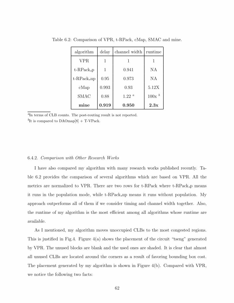
Table 6.2: Comparison of VPR, t-RPack, cMap, SMAC and mine.
algorithm delay channel width runtime
VPR 1 1 1
t-RPack p 1 0.941 NA
t-RPack up 0.95 0.973 NA
cMap 0.993 0.93 5.12X
SMAC 0.88 1.22 a 100x b
mine 0.919 0.950 2.3x
aIn terms of CLB counts. The post-routing result is not reported.bIt is compared to DAOmap[8] + T-VPack.
6.4.2. Comparison with Other Research Works
I have also compared my algorithm with many research works published recently. Ta-
ble 6.2 provides the comparison of several algorithms which are based on VPR. All the
metrics are normalized to VPR. There are two rows for t-RPack where t-RPack p means
it runs in the population mode, while t-RPack up means it runs without population. My
approach outperforms all of them if we consider timing and channel width together. Also,
the runtime of my algorithm is the most efficient among all algorithms whose runtime are
available.
As I mentioned, my algorithm moves unoccupied CLBs to the most congested regions.
This is justified in Fig.4. Figure 4(a) shows the placement of the circuit “tseng” generated
by VPR. The unused blocks are blank and the used ones are shaded. It is clear that almost
all unused CLBs are located around the corners as a result of favoring bounding box cost.
The placement generated by my algorithm is shown in Figure 4(b). Compared with VPR,
we notice the following two facts:
62
1) Along the northeast-directed diagonal, there are a lot of unused CLBs which are
dispersed more evenly and attracted to the most congested regions, i.e., the center
of the chip.
2) empty CLBs are still denser in the corners than at the center of the chip to reduce
wirelength. Distributing the empty CLBs this way will alleviate congestion and
thus reduce channel width.
63

Placement. Cost: 0.784987 bb_cost: 103.921 td_cost: 7.50444e-07 Channel Factor: 100 d_max: 5.38246e-08
(a) The placement of “tseng” by VPR.
Placement. Cost: 0.986473 bb_cost: 106.964 td_cost: 8.83274e-07 Channel Factor: 100 d_max: 4.93413e-08
(b) The placement of “tseng” by my algorithm.
Figure 6.4: The distribution of unoccupied blocks in the placements of VPR and my approach. I prefer (b) since it is more
balanced and is more liable to reduce channel width.
64

CHAPTER 7
CONCLUSIONS AND FUTURE WORK
In this thesis, I presented timing and congestion driven placement algorithms for field
programmable gate arrays (FPGAs). My approaches utilize the criticality history to improve
timing and disperse unoccupied blocks to alleviate congestion.
My first algorithm is based on congestion map. It reduces reduces channel width by
7.1%, and it does not degrade timing.
My second algorithm considers the history of timing-criticalities. It reduces the average
critical path delay by 11.8%, and channel width by 5.3%.
My final approach integrates these two algorithms and minimize the runtime. In sum-
mary, It reduces the average critical path delay by 8.1%, and channel width by 5%. Besides,
on average it needs only 2.3X runtime as of the Versatile Place and Route (VPR) suite, and
the ratio between my algorithm and VPR does not grow with the increasing circuit size.
The placement problem has been studied extensively in the past 30 years. However, recent
studies show that existing placement solutions are surprisingly far from optimal. Based on
the results from recent optimality and scalability studies of existing placement tools, Cong et
al. show that the results of leading placement tools from both industry and academia may be
up to 50% to 150% away from optimal in total wirelength [11]. If such a gap can be closed, the
corresponding performance improvement will be equivalent to several technology-generation
advancements. This is why we still need to spend great effort in placement research.
Another issue is to optimize multiple metrics simultaneously in placement because this
can enhance the overall performance of a circuit. Usually, we need to trade off among
multiple factors, such as timing, channel width, runtime and wirelength. In this work, I
found alleviation of congestion may benefit timing as well. In my future research, I would
like to further investigate the relationship and trade-off among multiple metrics.
65

BIBLIOGRAPHY
[1] C. J. Alpert, T. Chan, D. J.-H. Huang, I. Markov, and K. Yan, Quadratic placement re-
visited, Proceedings of the 34th annual conference on Design automation, 1997, pp. 752–
757.
[2] Charles J. Alpert, Tony F. Chan, Dennis J.-H. Huang, Andrew B. Kahng, Igor L. Markov,
Pep Mulet, and Kenneth Yan, Faster minimization of linear wirelength for global place-
ment, Proceedings of the international symposium on Physical design, 1997, pp. 4–11.
[3] Vaughn Betz, VPR and T-VPack users manual (version 4.30).
[4] Vaughn Betza and Jonathan Rose, VPR: A new packing, placement and routing tool for
FPGA research, FPL (1997), 213–222.
[5] Vaughn Betza, Jonathan Rose, and Alexander Marquardt, Architecture and cad for deep-
submicron FPGAs, Kluwer Academic Publishers, 1999.
[6] China Market Information Center, The field-programmable gate array (FPGA): Expand-
ing its boundaries, http://market.ccidnet.com/pub/enreport/show_9596.html.
[7] Y.-W. Chang and Y.-T. Chang, An architecture-driven metric for simultaneous place-
ment and global routing for FPGAs, Proceedings of the 37th Conference on Design
Automation, 2000, pp. 567–572.
[8] D. Chen and J. Cong, Daomap: a depth-optimal area optimization mapping algorithm
for FPGA designs, Proceedings of the 2004 IEEE/ACM International conference on
Computer-aided design, 2004, pp. 752–759.
[9] Chih-Liang Eric Cheng, RISA: Accurate and efficient placement routability modeling,
ICCAD (1994), 690–695.
66

[10] Paul Chow, Soon Ong Seo, Jonathan Rose, Kevin Chung, Gerard Paez, and Immanuel
Rahardja, The design of a SRAM-based field-programmable gate array, part II: circuit
design and layout, IEEE Trans. Very Large Scale Integr. Syst., vol. 7, 1999, pp. 321–330.
[11] Jason Cong, Joseph R. Shinnerl, Min Xie, Tim Kong, and Xin Yuan, Large-scale circuit
placement, ACM Trans. Des. Autom. Electron. Syst., vol. 10, 2005, pp. 389–430.
[12] Actel Corp., Programming antifuse devices.
[13] , Data book, 1999.
[14] Lattice Semiconductor corp., LatticeMico8 user’s guide.
[15] A. E. Dunlop, V. D. Agrawal, D. N. Deutsch, M. F. Jukl, P. Kozak, and M. Wiesel, Chip
layout optimization using critical path weighting, Proceedings of the 21st conference on
Design automation, 1984, pp. 133–136.
[16] A. E. Dunlop and B. W. Kernighan, A procedure for placement of standard cell vlsi
circuits, IEEE Transactions on Computer-Aided Design of Integrated Circuits, vol. 4,
1985, pp. 92–98.
[17] Takeo Hamada, Chung-Kuan Cheng, and Paul M. Chau, Prime: a timing-driven place-
ment tool using a piecewise linear resistive network approach, DAC (1993), 531–536.
[18] Jack Horgan, FPGA direction, http://www10.edacafe.com/nbc/articles/view_
weekly.php?articleid=209206.
[19] Dennis J.-H. Huang and Andrew B. Kahng, Partitioning-based standard-cell global place-
ment with an exact objective, Proceedings of the international symposium on Physical
design, 1997, pp. 18–25.
[20] Altera Inc., Configuration handbook.
[21] , Nios II processor reference handbook (ver 6.0, may 2006).
[22] , Data book, 1999.
[23] Atmel Inc., AT94KAL series field programmable system level integrated circuit.
[24] MathStar Inc., What is an FPOA?, http://www.mathstar.com/overview.html.
[25] Stretch Inc., S5530 data sheet (version 1.2).
67
[26] Xilinx Inc., Architecture, http://www.xilinx.com/products/silicon_solutions/
fpgas/spartan_series/s%partan2_fpgas/capabilities/architecture.htm.
[27] , Configuration overview, http://toolbox.xilinx.com/docsan/xilinx7/
help/iseguide/html/ise_configu%ration_overview.htm.
[28] , MicroBlaze processor reference guide.
[29] , PicoBlaze 8-bit microcontroller for Virtex-II series devices.
[30] , Virtex-4 Family Overview.
[31] R. Dorf J. Oldfield, Field-programmable gate arrays: Reconfigurable logic for rapid pro-
totyping and implementation of digital systems, WileyInterscience, 1995.
[32] S. Brown J. Rose, Flexibility of interconnection structures for field-programmable gate
arrays, IEEE J. Solid-State Circuits, vol. 26, 1991, pp. 277–282.
[33] M. Jackson and E. S. Kuh, Performance-driven placement of cell based ic’s, DAC (1989),
370–375.
[34] M. Khellah, S. Brown, and Z. Vranesic, Modelling routing delays in SRAM-based FP-
GAs, Canadian Conference on VLSI, 1993, pp. 6B.13–6B.18.
[35] S. Kirkpatrick, C. D. Gelatt, and M.P. Vecchi, Optimization by simulated annealing,
Science, 1983, pp. 671–680.
[36] J. M. Kleinhans, G. Sigl, F. M. Johannes, and K. J. Antreich, GORDIAN: Vlsi placement
by quadratic programming and slicing optimization, IEEE Trans. on Computer-Aided
Design, 1991, pp. 356–365.
[37] T. Kong, A novel net weighting algorithm for timing-driven placement, Proceedings
of the 2002 IEEE/ACM International Conference on Computer-Aided Design, 2002,
pp. 172–176.
[38] Ian Kuon and Jonathan Rose, Measuring the gap between FPGAs and ASICs, FPGA
(2006), 21–30.
68

[39] J. Y. Lin, D. Chen, and J. Cong, Optimal simultaneous mapping and clustering for fpga
delay optimization, Proceedings of the 43rd annual conference on design automation,
2006, pp. 472–477.
[40] Alexander Marquardt, Vaughn Betz, and Jonathan Rose, Timing-driven placement for
FPGAs, FPGA (2000), 203–213.
[41] University of Toronto, http://www.eecg.toronto.edu/~vaughn/vpr/vpr.html.
[42] , The FPGA place-and-route challenge, http://www.eecg.toronto.edu/
~vaughn/challenge/challenge.html.
[43] H. Ren, D. Z. Pan, and D. S. Kung, Sensitivity guided net weighting for placement driven
synthesis, Proceedings of the 2004 International Symposium on Physical Design, 2004,
pp. 10–17.
[44] Haoxing Ren, David Z. Pan, and David S. Kung, Sensitivity guided net weighting for
placement driven synthesis, Proceedings of the international symposium on Physical
design, 2004, pp. 10–17.
[45] B. M. Riess and G. G. Ettelt, Speed: Fast and efficient timing driven placement, IEEE
International Symposium on Circuits and Systems, 1995, pp. 377–380.
[46] J. Rose, W. Snelgrove, and Z. Vranesic, ALTOR: An automatic standard cell layout
program, Canadian Conference on VLSI, 1985, pp. 169–173.
[47] C. Sechen and K. W. Lee, An improved simulated annealing algorithm for row-based
placement, Proceedings of the IEEE International Conference on Computer Aided De-
sign, 1987, pp. 478–481.
[48] Carl Sechen and Alberto Sangiovanni-Vincentelli, The TimberWolf placement and rout-
ing package, IEEE Journal of Solid-State Circuits, 1985, pp. 510–522.
[49] , TimberWolf3.2: a new standard cell placement and global routing package, Pro-
ceedings of the 23rd ACM/IEEE conference on Design automation, 1986, pp. 432–439.
69

[50] Georg Sigl, Konrad Doll, and Frank M. Johannes, Analytical placement: A linear or a
quadratic objective function?, Proceedings of the 28th conference on ACM/IEEE design
automation, 1991, pp. 427–432.
[51] A. Srinivasan, K. Chaudhary, and E. S. Kuh, RITUAL: A performance driven placement
algorithm for small cell ic’s, DAC (1991), 45–51.
[52] Arvind Srinivasan, An algorithm for performance-driven initial placement of small-
cell ICs, Proceedings of the 28th conference on ACM/IEEE design automation, 1991,
pp. 636–639.
[53] Wern-Jieh Sun and Carl Sechen, Efficient and effective placement for very large circuits,
Proceedings of the IEEE/ACM international conference on Computer-aided design, 1993,
pp. 170–177.
[54] William Swartz and Carl Sechen, Timing driven placement for large standard cell cir-
cuits, Proceedings of the 32nd ACM/IEEE conference on Design automation, 1995,
pp. 211–215.
[55] Lucent Technologies, Fpga data book, 1998.
[56] Russell Tessier, Fast placement approaches for FPGAs, ACM Trans. Des. Autom. Elec-
tron. Syst. 7 (2002), no. 2, 284–305.
[57] Natarajan Viswanathan, Min Pan, and Chris Chu, Fastplace 2.0: an efficient analytical
placer for mixed-mode designs, Proceedings of the conference on Asia South Pacific design
automation, 2006, pp. 195–200.
[58] Q. Wang, J. Lillis, and S. Sanyal, An LP-based methodology for improved timing-driven
placement, Proceedings of the 2005 Conference on Asia South Pacific Design Automation,
2005, pp. 1139–1147.
[59] Wikipedia, Field-programmable gate array, http://en.wikipedia.org/wiki/FPGA.
[60] Michael G. Wrighton and A. M. DeHon, Hardware-assisted simulated annealing with
application for fast fpga placement, Proceedings of the 2003 ACM/SIGDA eleventh in-
ternational symposium on Field programmable gate arrays, 2003, pp. 33–42.
70
[61] Zhong Xiu, James D. Ma, Suzanne M. Fowler, and Rob A. Rutenbar, Large-scale place-
ment by grid-warping, Proceedings of the 41st annual conference on Design automation,
2004, pp. 351–356.
[62] Zhong Xiu and Rob A. Rutenbar, Timing-driven placement by grid-warping, Proceedings
of the 42nd annual conference on Design automation, 2005, pp. 585–591.
71