Embed Size (px)
Citation preview

Throughput, power consumption and interferenceconsiderations in visible light communicationDeng, X.
Published: 25/04/2018
Document VersionPublisher’s PDF, also known as Version of Record (includes final page, issue and volume numbers)
Please check the document version of this publication:
• A submitted manuscript is the author's version of the article upon submission and before peer-review. There can be important differencesbetween the submitted version and the official published version of record. People interested in the research are advised to contact theauthor for the final version of the publication, or visit the DOI to the publisher's website.• The final author version and the galley proof are versions of the publication after peer review.• The final published version features the final layout of the paper including the volume, issue and page numbers.
Link to publication
Citation for published version (APA):Deng, X. (2018). Throughput, power consumption and interference considerations in visible light communicationEindhoven: Technische Universiteit Eindhoven
General rightsCopyright and moral rights for the publications made accessible in the public portal are retained by the authors and/or other copyright ownersand it is a condition of accessing publications that users recognise and abide by the legal requirements associated with these rights.
• Users may download and print one copy of any publication from the public portal for the purpose of private study or research. • You may not further distribute the material or use it for any profit-making activity or commercial gain • You may freely distribute the URL identifying the publication in the public portal ?
Take down policyIf you believe that this document breaches copyright please contact us providing details, and we will remove access to the work immediatelyand investigate your claim.
Download date: 11. Sep. 2018

Throughput, Power Consumption and InterferenceConsiderations in Visible Light Communication
PROEFSCHRIFT
ter verkrijging van de graad van doctor aan de Technische UniversiteitEindhoven, op gezag van de rector magnificus prof.dr.ir. F.P.T.Baaijens,voor een commissie aangewezen door het College voor Promoties, in het
openbaar te verdedigen op woensdag 25 april 2018 om 13:30 uur
door
Xiong Deng
geboren te Sichuan, China

Dit proefschrift is goedgekeurd door de promotoren en de samenstelling van de pro-motiecommissie is als volgt:
voorzitter : prof.dr.ir. J.H. Blom1e promotor : prof.dr.ir. J.P.M.G. Linnartz2e promotor : prof.dr. Guofu Zhoucopromotor : dr. Yan Wuleden : prof.dr.ir. S. Hranilovic (McMaster University, Canada)
prof.dr.ir. L. Van der Perre (KU Leuven, Belgie)prof.dr.ir. S.M. Heemstra de Grootdr.ir. T.J. Tjalkens
Het onderzoek of ontwerp dat in dit proefschrift wordt beschreven is uitgevoerd in overeen-stemming met de TU/e Gedragscode Wetenschapsbeoefening.

Throughput, Power Consumption andInterference Considerations in Visible Light
Communication
Xiong Deng

Throughput, Power Consumption and Interference Considerations in Visible Light Com-munication / by Xiong Deng – Eindhoven : Eindhoven University of Technology, 2018.A catalogue record is available from the Eindhoven University of Technology Library.ISBN : 978-90-386-4474-5.
The research presented in this thesis was supported by Philips Group Innovation – Re-search, Eindhoven, The Netherlands.
Cover Design : Xiong Deng, Eindhoven, The Netherlands.Reproduction : Eindhoven University of Technology.
Copyright c© 2018, Xiong DengAll rights reserved. Copyright of the individual chapters belongs to the publisher of thejournal listed at the beginning of each respective chapter. No part of this publicationmay be reproduced, stored in a retrieval system, or transmitted, in any form or by anymeans, electronic, mechanical, photocopying, recording or otherwise, without the priorwritten permission from the copyright owner.

To my beloved parentsto my beloved wife
to my lovely sonand to my country, China

Summary
With the increasingly crowded Radio Frequency (RF) spectrum due to the surging wire-less data transmission, Optical Wireless Communication (OWC) becomes a promisingcomplementary technique for existing RF communications. Using the wavelengths in theinfrared, visible and ultraviolet regions of the spectrum, OWC is being extensively ex-plored for short, medium and long range data transmissions. Thanks to the fast growingSolid-State Lighting (SSL) technology in recent years, Light Emitting Diodes (LEDs)have fueled the research on Visible Light Communications (VLC) and Light Fidelity(LiFi). As a subcategory of OWC, VLC and LiFi can provide data transmission via theillumination LEDs. Nevertheless, several challenges are raised in a Joint Illuminationand Communication (JIC) system using LED, including the throughput, power penaltyand interference. To be specific, when a lighting system is adopted for communication,the driving current through the LED is modulated by a data signal along with a light-ing control signal. This current modulation results in several consequences. Firstly, theachievable speed of the data modulation is limited by the LED bandwidth which is onlyseveral MHz in a commercial illumination LED. Secondly, the data modulation inducesextra power losses both in LEDs and drivers which are out of the power budget of thelighting system. Thirdly, the current fluctuation, induced by the data signal and light-ing control signal, introduces interference to the communication system as well as otherequipment that applies light as input signal. The challenges aforementioned have moti-vated the investigation of the achievable date rate, the power penalty and the interferenceeffect in a JIC system, preferably, to elaborate a system design with high data rate, highpower efficiency and interference free.
To boost the data throughput, we deal with the transient response of the LED, basedon the physical mechanism in the quantum well. Through a dynamic differential equa-tion, both the LED low-pass effect and nonlinearity that limit the data throughput areinvestigated. On one hand, the low-pass effect can be reduced by Digital Signal Pro-cessing (DSP) techniques such as a linear equalization in the receiver. On the otherhand, to overcome the LED nonlinearity, a novel nonlinear predistorter and parameterestimation approach are proposed for practical implementation. The proposed predistor-
vii
viii Summary
tion and estimation are further validated within the On-Off Keying (OOK) and four-levelPulse-Amplitude Modulation (PAM-4) systems. The results show that the data rate issignificantly enhanced when using a band-limited LED.
The extra power penalty induced by the data modulation in a JIC transmitter isquantified. The key components that potentially induce extra power in the transmitter aretaken into account in the analysis, including the Switched Mode Power Supply (SMPS),the signal modulator and the LEDs. We propose an effective metric in terms of ExtraEnergy Per Symbol (EEPS) to evaluate the JIC system performance. For instance, theEEPS of a JIC transmitter for Orthogonal Frequency-Division Multiplexing (OFDM)system is much higher than that of a 2-PAM one, which means that although the OFDMcan achieve higher throughput but it needs more extra power. Besides, we also explore thepossibility to improve the energy efficiency of the JIC transmitter. For a low data rate,we proposed an efficient transmitter by adapting the driver control loop. For high datarate, we realized an efficient OFDM transmitter by using a SMPS and a serial modulator.Particularly, in the LED, an empirical design rule was proposed to avoid substantial extrapower loss, according to the power budget for communication.
We classify the effect of the current fluctuation into two categories, namely the inter-ference of VLC, e.g., ripple from the SMPS into VLC, and the cross-interference of otherequipment that applies light as input signal. In the first category, we present a new sys-tem model with Binary Phase Modulation (BPM), by considering the current fluctuationintroduced by the SMPS as an important noise contribution. The fluctuation randomlyaffects the distance between the signal and the decision threshold, so that the Bit ErrorRate (BER) of the received data is increased according to the strength of fluctuation.We further propose approximations for the fluctuation interference, including a Gaussianapproximation and a Delta function approximation. Both the BER analysis and interfer-ence approximations are verified by Monte-Carlo simulations. In the second category, weaddress the reading failure of a barcode scanner that suffers from interferences of LEDlamps. In particular, the barcode scanner is treated as a special communication systemusing light. The reading performance is modeled in terms of Timing Signal-to-InterferenceRatio (TSIR), in particular, as a function of modulation depth and frequency of the in-terference in the LED lighting. The LED interference, generated in the SMPS, was foundneither additive nor Gaussian interference with frequency up to several MHz and it couldseriously affect the barcode reading performance. We also propose an empirical FlickerInterference Metric (FIM) concerning the multi-frequencies interference, e.g. harmonicsof the SMPS control signal. Both the TSIR and FIM are validated through experiments.
In summary, this thesis focuses on addressing the challenges in VLC physical layer withreusing the illumination systems. It shows that the data throughput can be extendedby novel DSP techniques; the power penalty for communication can be minimized bydedicated circuits and system designs; and the interference could be quantified or reducedonce its effect was predicted.

List of abbreviations
AWGN Additive White Gaussian NoiseALI Ambient Light InterferenceANN Artificial Neural NetworkAC Alternating CurrentADC Analog to Digital ConverterASK Amplitude Shift KeyingBER Bit Error RateBPM Binary Phase ModulationCFF Critical Flicker FrequencyCCT Correlated Color TemperatureCRI Color Rendering IndexCCD Charge-Coupled DeviceCCM Continuous Conduction ModeCSK Color-Shift KeyingCDMA Code Division Multiple AccessDAC Digital to Analog ConverterDCO-OFDM DC-biased optical OFDMDMT Discrete Multi ToneDFE Decision Feedback EqualizerDH Double Hetero-structureDCM Discontinuous Conduction ModeEQE External Quantum EfficiencyEOE Electrical-Optical ElectricalEEPS Extra Energy Per SymbolESR Equivalent Series ResistanceES Energy per SymbolEMI Electro-Magnetic InterferenceFEC Forward Error CorrectionFET Field Effect Transistor
ix

x List of abbreviations
FOV Field Of ViewFIR Finite Impulse ResponseFIM Flicker Interference MetricFLI Fluorescent Light InterferenceGbps Giga bits per secondGsps Giga Samples Per SecondGZO Gallium-doped Zinc OxideHPF High-Pass FilteringIM/DD Intensity Modulation/Direct DetectionIQE Internal Quantum EfficiencyISI Inter Symbol InterferenceIEC International Electrotechnical CommissionIIR Infinite Impulse ResponseJIC Joint Illumination and CommunicationKbps Kilobits per secondLED Light Emitting DiodeLOS Line Of SightLER Luminous Efficacy of RadiationLPF Low Pass FilterLMS Least Mean SquareLiFi Light FidelityLTI Linear Time InvariantMIMO Multiple Input Multiple OutputMbps Million bits per secondMEMS Micro Electro Mechanical SystemsMLSE Maximum-Likelihood Sequence EstimationMMSE Minimum Mean Square ErrorMF Matched FiltersOWC Optical Wireless CommunicationsOFDM Orthogonal Frequency Division MultiplexingOCC Optical Cameras CommunicationOOK On Off KeyingOLED Organic Light Emitting DiodesPAPR Peak to Average Power RatioPPM Pulse Position ModulationPAM Pulse Amplitude ModulationPWM Pulse Width ModulationPhC Photonic CrystalPD Photo DiodePA Power AmplifierPSD Power Spectrum Density

List of abbreviations xi
PC-LED Phosphor Converted LEDQAM Quadrature Amplitude ModulationQW Quantum WellQR Quick ResponseRF Radio FrequencyRGB Red Green BlueRLL Run Length LimitedRMS Root Mean SquareRS Reed-Solomon CodingRLS Recursive Least SquaresSER Symbol Error RateSDM Space Division MultiplexSRH Shockley-Read-HallSSL Solid-State LightingSNR Signal to Noise RatioSMPS Switched Mode Power SupplySMPSs Switched Mode Power SuppliesSPD Spectral Power DistributionSIR Signal-to-Interference RatioSerial-F Serial FETTLAs Temporal Light ArtefactsTSIR Timing Signal-to-Interference RatioTIA Trans-Impedance AmplifierTHz TeraHertzUPC Universal Product CodeVLC Visible Light CommunicationVPPM Variable Pulse Position ModulationWDM Wavelength Division MultiplexingWPE Wall-Plug EfficiencyZF Zero-forcing

xii List of abbreviations

List of notations
E [x] Expected value of x∆E Extra Energy Per Symbol (EEPS)ΦV Luminous flux outputn LED ideality factork Boltzmann constantT Temperature in Kelvinq Charge of ElectronIs LED saturation currentRL Equivalent Series Resistance (ESR)RDyn Dynamic resistanceAnr SRH recombination coefficientBr Radiative recombination coefficientCnr Auger recombination coefficienttw Active layer thicknessAw Active layer areap0 Doping concentrationEp Energy of photon (650nm)Ts Sampling periodαrms Root-mean-square modulation indexαpeak Peak modulation indexη Efficiencyε Responsivity of the PDµ Responsivity of the LEDρ Optical channel DC gainA Surface area of the PDAd Effect aperture of PDP PowerΦ1/2 Semi-angle at half power
xiii

xiv Contents

Contents
Summary vii
List of abbreviations ix
List of notations xiii
1 General introduction 11.1 Introduction . . . . . . . . . . . . . . . . . . . . . . . . . . . . . . . . . . . . . . . 2
1.1.1 Optical Wireless Communications . . . . . . . . . . . . . . . . . . . . . . . 21.1.2 Visible Light Communications . . . . . . . . . . . . . . . . . . . . . . . . . 3
1.2 Challenges in VLC . . . . . . . . . . . . . . . . . . . . . . . . . . . . . . . . . . . 51.2.1 Throughput . . . . . . . . . . . . . . . . . . . . . . . . . . . . . . . . . . 51.2.2 Power . . . . . . . . . . . . . . . . . . . . . . . . . . . . . . . . . . . . . . 61.2.3 Interference . . . . . . . . . . . . . . . . . . . . . . . . . . . . . . . . . . . 6
1.3 Motivation and Objective . . . . . . . . . . . . . . . . . . . . . . . . . . . . . . . . 71.4 Outline and Contributions of the thesis . . . . . . . . . . . . . . . . . . . . . . . . 8
1.4.1 Outline . . . . . . . . . . . . . . . . . . . . . . . . . . . . . . . . . . . . . 81.4.2 Contributions . . . . . . . . . . . . . . . . . . . . . . . . . . . . . . . . . . 8
Part I: Throughput in Visible Light Communication using LED 14
2 Mitigating LED Nonlinearity to Enhance Visible Light Communications 172.1 Introduction . . . . . . . . . . . . . . . . . . . . . . . . . . . . . . . . . . . . . . . 182.2 LED response model . . . . . . . . . . . . . . . . . . . . . . . . . . . . . . . . . . 19
2.2.1 Rate equation for carrier recombination in LED . . . . . . . . . . . . . . . 212.2.2 Radiative recombination Rr(t) . . . . . . . . . . . . . . . . . . . . . . . . 212.2.3 Non-radiative recombination Rnr(t) . . . . . . . . . . . . . . . . . . . . . . 232.2.4 Numerical LED nonlinear model . . . . . . . . . . . . . . . . . . . . . . . . 23
2.3 LED response with linear approximation . . . . . . . . . . . . . . . . . . . . . . . . 242.3.1 Static memoryless nonlinearity due to efficiency droop . . . . . . . . . . . . 25
xv

xvi Contents
2.3.2 Transient memory nonlinearity with linear approximation . . . . . . . . . . . 252.4 Overcome the LED nonlinearity . . . . . . . . . . . . . . . . . . . . . . . . . . . . 27
2.4.1 Decision feedback equalization . . . . . . . . . . . . . . . . . . . . . . . . 282.4.2 Non-linear predistortion . . . . . . . . . . . . . . . . . . . . . . . . . . . . 29
2.5 Channel capacity of a linear low-pass channel . . . . . . . . . . . . . . . . . . . . . 312.6 Non-linear parameters estimation . . . . . . . . . . . . . . . . . . . . . . . . . . . 322.7 Simulations and Validation . . . . . . . . . . . . . . . . . . . . . . . . . . . . . . . 33
2.7.1 Convergence of Euler’s method . . . . . . . . . . . . . . . . . . . . . . . . 332.7.2 LED nonlinear effect on OOK system . . . . . . . . . . . . . . . . . . . . . 342.7.3 LED nonlinear effect on PAM-4 system . . . . . . . . . . . . . . . . . . . . 362.7.4 Non-linear predistortion . . . . . . . . . . . . . . . . . . . . . . . . . . . . 382.7.5 Parameter estimation . . . . . . . . . . . . . . . . . . . . . . . . . . . . . 392.7.6 LED nonlinearity and non-linear predistortion in OFDM system . . . . . . . 42
2.8 Conclusions . . . . . . . . . . . . . . . . . . . . . . . . . . . . . . . . . . . . . . . 43
Part II: Power Consumption in Visible Light Communication Adopting LEDLighting 45
3 Modelling and Analysis of Transmitter Performance for High-Speed VisibleLight Communications 473.1 Introduction . . . . . . . . . . . . . . . . . . . . . . . . . . . . . . . . . . . . . . . 473.2 Power consumption in LED . . . . . . . . . . . . . . . . . . . . . . . . . . . . . . . 50
3.2.1 Power consumption in LED without modulation . . . . . . . . . . . . . . . 503.2.2 Extra power consumption in LED for modulation . . . . . . . . . . . . . . . 51
3.3 Power consumption in modulator . . . . . . . . . . . . . . . . . . . . . . . . . . . 533.3.1 Extra supply power in Bias-T transmitter . . . . . . . . . . . . . . . . . . . 533.3.2 Power consumption in Serial-F transmitter . . . . . . . . . . . . . . . . . . 563.3.3 Proposed metric of Extra Energy Per Symbol (EEPS) . . . . . . . . . . . . 593.3.4 Comparison between Bias-T and Serial-F transmitter . . . . . . . . . . . . 59
3.4 Losses in the SMPS for DC . . . . . . . . . . . . . . . . . . . . . . . . . . . . . . 613.4.1 Transmitter power efficiency . . . . . . . . . . . . . . . . . . . . . . . . . . 613.4.2 Summary for Serial-F transmitter . . . . . . . . . . . . . . . . . . . . . . . 62
3.5 Communication performance . . . . . . . . . . . . . . . . . . . . . . . . . . . . . . 643.5.1 VLC Channel Model . . . . . . . . . . . . . . . . . . . . . . . . . . . . . . 643.5.2 Received energy per symbol . . . . . . . . . . . . . . . . . . . . . . . . . . 653.5.3 Receiver BER Performance . . . . . . . . . . . . . . . . . . . . . . . . . . 66
3.6 Numerical and Simulation Results . . . . . . . . . . . . . . . . . . . . . . . . . . . 673.6.1 Extra power loss in LED . . . . . . . . . . . . . . . . . . . . . . . . . . . . 683.6.2 Supply power in Bias-T and Serial-F transmitter . . . . . . . . . . . . . . . 683.6.3 Efficiency of Serial-F transmitter using SMPS . . . . . . . . . . . . . . . . 703.6.4 Communication performance with power penalty . . . . . . . . . . . . . . . 72
3.7 Conclusion . . . . . . . . . . . . . . . . . . . . . . . . . . . . . . . . . . . . . . . 76

Contents xvii
4 LED Power Consumption in Joint Illumination and Communication System 774.1 Introduction . . . . . . . . . . . . . . . . . . . . . . . . . . . . . . . . . . . . . . . 784.2 LED luminous flux versus current nonlinearity (ΦINL) . . . . . . . . . . . . . . . . 79
4.2.1 Luminous flux of LED versus current . . . . . . . . . . . . . . . . . . . . . 804.2.2 Thermal effect on LED luminous flux . . . . . . . . . . . . . . . . . . . . . 82
4.3 Extra power loss due to ΦINL and modulation . . . . . . . . . . . . . . . . . . . . 834.3.1 Luminous flux of a commercial white LED . . . . . . . . . . . . . . . . . . 834.3.2 Extra power for luminous flux compensation . . . . . . . . . . . . . . . . . 83
4.4 Extra power loss due to PINL and modulation . . . . . . . . . . . . . . . . . . . . . 864.4.1 Binary modulation . . . . . . . . . . . . . . . . . . . . . . . . . . . . . . . 864.4.2 Continuous modulation . . . . . . . . . . . . . . . . . . . . . . . . . . . . 87
4.5 Numerical Results . . . . . . . . . . . . . . . . . . . . . . . . . . . . . . . . . . . . 874.5.1 Extra power loss of the LED . . . . . . . . . . . . . . . . . . . . . . . . . . 874.5.2 LED efficacy for joint illumination and communication . . . . . . . . . . . . 89
4.6 Conclusion . . . . . . . . . . . . . . . . . . . . . . . . . . . . . . . . . . . . . . . 89
Part III: Interference Considerations in Visible Light Communication 90
5 Performance Analysis for Joint Illumination and Visible Light Communica-tion using Buck Driver 935.1 Introduction . . . . . . . . . . . . . . . . . . . . . . . . . . . . . . . . . . . . . . . 945.2 System Description . . . . . . . . . . . . . . . . . . . . . . . . . . . . . . . . . . . 955.3 BER Analysis for BPM in VLC . . . . . . . . . . . . . . . . . . . . . . . . . . . . . 96
5.3.1 Description of the transmission signal . . . . . . . . . . . . . . . . . . . . . 965.3.2 VLC channel model . . . . . . . . . . . . . . . . . . . . . . . . . . . . . . 975.3.3 Received BER performance . . . . . . . . . . . . . . . . . . . . . . . . . . 98
5.4 LED Driver Model for BPM . . . . . . . . . . . . . . . . . . . . . . . . . . . . . . 995.4.1 Energy efficiency of control-loop adapting . . . . . . . . . . . . . . . . . . 1005.4.2 Energy efficiency of binary shunting . . . . . . . . . . . . . . . . . . . . . . 102
5.5 Effect of Ripple Interference on BER . . . . . . . . . . . . . . . . . . . . . . . . . . 1035.5.1 Ripple interference . . . . . . . . . . . . . . . . . . . . . . . . . . . . . . . 1035.5.2 Ripple interference after matched filtering . . . . . . . . . . . . . . . . . . 1045.5.3 BER performance with ripple interference . . . . . . . . . . . . . . . . . . . 1075.5.4 Approximation of ripple interference . . . . . . . . . . . . . . . . . . . . . . 1085.5.5 Improved symbol filtering . . . . . . . . . . . . . . . . . . . . . . . . . . . 109
5.6 Numerical and Simulation Results . . . . . . . . . . . . . . . . . . . . . . . . . . . 1095.6.1 BER performance of BPM . . . . . . . . . . . . . . . . . . . . . . . . . . . 1105.6.2 Power consumption and efficiency of LED drivers . . . . . . . . . . . . . . 1115.6.3 Communication performance versus power consumption . . . . . . . . . . . 1135.6.4 BER performance with power and ripple consideration . . . . . . . . . . . . 115
5.7 Conclusion . . . . . . . . . . . . . . . . . . . . . . . . . . . . . . . . . . . . . . . 116

xviii Contents
6 Reading Analysis for Barcode Scanner with Interference from LED-basedLighting 1196.1 Introduction . . . . . . . . . . . . . . . . . . . . . . . . . . . . . . . . . . . . . . . 1206.2 System description of barcode scanners . . . . . . . . . . . . . . . . . . . . . . . . 1216.3 System model for laser scanners . . . . . . . . . . . . . . . . . . . . . . . . . . . . 123
6.3.1 Transmitter . . . . . . . . . . . . . . . . . . . . . . . . . . . . . . . . . . . 1236.3.2 Channel . . . . . . . . . . . . . . . . . . . . . . . . . . . . . . . . . . . . . 1236.3.3 Receiver . . . . . . . . . . . . . . . . . . . . . . . . . . . . . . . . . . . . 126
6.4 Signal and performance analysis for laser scanners . . . . . . . . . . . . . . . . . . 1276.4.1 Signal description . . . . . . . . . . . . . . . . . . . . . . . . . . . . . . . 1276.4.2 Signal enhancement . . . . . . . . . . . . . . . . . . . . . . . . . . . . . . 1286.4.3 Signal for peak and edge detection . . . . . . . . . . . . . . . . . . . . . . 1296.4.4 Received interference from LED . . . . . . . . . . . . . . . . . . . . . . . . 1306.4.5 Error models . . . . . . . . . . . . . . . . . . . . . . . . . . . . . . . . . . 132
6.5 Experimental validation . . . . . . . . . . . . . . . . . . . . . . . . . . . . . . . . . 1346.5.1 TSIR . . . . . . . . . . . . . . . . . . . . . . . . . . . . . . . . . . . . . . 1356.5.2 Sensitivity versus frequency . . . . . . . . . . . . . . . . . . . . . . . . . . 1366.5.3 Sensitivity under multi-frequency . . . . . . . . . . . . . . . . . . . . . . . 137
6.6 Conclusion . . . . . . . . . . . . . . . . . . . . . . . . . . . . . . . . . . . . . . . 139
7 General discussions and future research 1417.1 General discussions . . . . . . . . . . . . . . . . . . . . . . . . . . . . . . . . . . . 1427.2 Recommendations for future research . . . . . . . . . . . . . . . . . . . . . . . . . 142
7.2.1 High-speed VLC . . . . . . . . . . . . . . . . . . . . . . . . . . . . . . . . 1437.2.2 VLC transceivers design with high speed and efficiency . . . . . . . . . . . 1457.2.3 Effect of current modulation on LED lifetime and human perception . . . . 145
A Concavity of LED output light versus current with ABC model 165
B Small signal performance of Class A and Class B amplifier 169B.1 FET I-V curve . . . . . . . . . . . . . . . . . . . . . . . . . . . . . . . . . . . . . . 169B.2 Class A amplifier . . . . . . . . . . . . . . . . . . . . . . . . . . . . . . . . . . . . 170B.3 Class B amplifier . . . . . . . . . . . . . . . . . . . . . . . . . . . . . . . . . . . . 172
List of the author’s publications 175
Acknowledgements 177
About the author 179

CHAPTER 1
General introduction
“Light not only gives us the vision, but also the enlightenment of our thoughts.”— The author, Eindhoven, The Netherlands, 2017.
1

2 Chapter 1. General introduction
1.1 Introduction
1.1.1 Optical Wireless Communications
Although communications via light is already an age-old concept, Optical Wireless Com-munications (OWC) is a promising technology that enables the information exchanges inan unguided channel using the carriers in the optical spectrum. The historical forms ofOWC include the beacon fires, smoke, ship flags and semaphore [74, 89]. The first formalOWC was the well-known photophone for transmitting voice over a wireless light wave,invented by Alexander Graham Bell in 1880 [52]. After that, the OWC fortune has beenchanged since the early 1960s when the optical sources such as laser were discovered [54].Most recently, thanks to the fast growing Solid-State Lighting (SSL) technology, therehas been a surge of interest in data transmission adopting the ubiquitous Light EmittingDiode (LED) lighting. In general, OWC has emerged as a promising solution to the ”lastmile” bottleneck both for indoor and outdoor communications in the fifth generation (5G)networks.
OWC uses optical wavelengths in the infrared, visible, and ultraviolet regions of thespectrum, as shown in Figure 1.1. It has the potential to provide up to TeraHertz (THz)of unlicensed bandwidth, although state of the art is mostly to modulate the intensity ofthe full spectrum with relative low data rate. VLC offers a number of unique advantagesover its Radio Frequency (RF) counterpart, such as unregulated bandwidth for highdata rate, a high degree of spatial reuse, secure connectivity, absence of electromagneticinterference and the potential combination with existing lighting [54, 81]. A generalcomparison between OWC and RF is listed in Table 1.1 [54, 55].
108
Wavelength (m)
106 104 102 100 10-2 10-4 10-6 10-8 10-10 10-12 10-14 10-16 10-18
100 102 104 106 108 1010 1012 1014 1016 1018 1020 1022 1024 1026
Po
wer
Ca
ble
s
Radio waves Microwaves
Long
Waves
Medium
Waves
Sh
ort
Wa
ves
TV
FM
Cel
l P
ho
nes
GP
S
Ra
da
rs
Infra
Red
Ultra
Violet
Visible Light750nm 350nm
OWC band
Fibre Optics X Rays
Gamma Rays
Cosmic Rays
Frequency (Hz)
Figure 1.1: OWC in electromagnetic spectrum (Adapted from [1])
Due to the unique characteristics and the advantages over RF, there is a wide range ofOWC applications, including a very short range (mm range) optical interconnect withinintegrated circuits, high-volume ubiquitous consumer electronic products, indoor naviga-tion systems, indoor high-speed transmission, outdoor intra-building links (a few kilome-ter range), inter-satellite links (several thousand kilometers range), under water commu-nications and deep space communications, etc [54].

Chapter 1. General introduction 3
Table 1.1: Comparison Between OWC and RF Communication Systems
Property OWC RFData rate Low-High LowDistance Short-Long Short-LongCoverage Narrow-Wide Narrow-WideMultipath fading No YesPath-loss High HighMobility Limited HighNoise Background light All electrical devicesFrequency Regulation No YesPower consumption Low MediumSecurity High LowElectromagnetic Interference No YesNetwork Scalable Non-scalableDevice size Small Large
1.1.2 Visible Light Communications
Visible light communications (VLC) is a subcategory of OWC operating in the visibleregion of the spectrum (380-780 nm of wavelength). The emerging VLC has attractedmuch attention for indoor wireless communications due to the widely employment ofLEDs. The first VLC using LED was demonstrated in 1999, where an audio signal wastransmitted using visible light [143]. After more than a decade evolution of the VLC, in2011, VLC protocols and PHY layer were proposed in the IEEE standard 802.15.7, wherethe data communication and lighting application were merged [2]. Some shortcomings ofthe standard, e.g., the data rate was limited to only 96 Mbps, have led to the developmentof a revised version, i.e., IEEE 802.15.7r1 [163]. Moreover, the VLC has been consideredas a potential access option for 5G wireless communications [188]. It can be foreseen thatthe VLC would become a complementary technology to RF techniques, in particular, forthe indoor wireless data transmission.
The main driver behind VLC is the increasing presence of LEDs in ubiquitous lightinginfrastructure [59]. It is widely expected that LEDs will dominate future illuminationmarket because they have several advantageous properties over traditional light sources,for instance, high brightness, high energy efficiency, high reliability, long life time andcolor rendering capability [3, 81, 94]. Several commonly used LEDs are listed in Table1.2, along with their key features [86]. As we can see, the Micro LED (µ-LED) has thehighest bandwidth while at the cost of high price and the highest complexity, and theOrganic LED (OLED) is quite bandwidth limited with the lowest cost. In particular, thePhosphor Converted LEDs (PC-LED) and multi-chip RGB-LEDs, where Red, Green andBlue (RGB) are combined, are mostly used for illumination due to their high efficacy.
Besides the characteristics inherited from the OWC, VLC has the potential to provide

4 Chapter 1. General introduction
Table 1.2: Comparison of Commonly Used LEDs
Property PC-LED RGB-LED µ-LED OLEDBandwidth 3-5 MHz 10-20 MHz ≥300 MHz ≤1 MHzEfficacy 130 lm/W 65 lm/W N/A 45 lm/WCost Low High High LowestComplexity Low Moderate Highest High
data transmission via the illumination LEDs. The primary illumination functionality ofLED will not be affected by modulation as long as the frequency of the data modula-tion is above the flicker fusion threshold of human eye sensitivity [81, 162]. All theseunique characteristics made VLC of increasing interest and thus they are appealing fora wide range of applications such as indoor broadband access [45], indoor positioning[191], distributed lighting remote control [168], entertainment interaction [175], under-water communications [181], vehicular-to-vehicular communications [190] and dense cellnetworks [163]. Figure 1.2 shows the concept of a smart office lighting scenario usingVLC with Ethernet enabled in the future, where all the smart devices, office appliancesand household appliances with photodiodes will be connected to the network through thelight [145, 168].
Pad
SwitchSmart
phone
Thermometer
TV and
Telegram
LED lamps
Copier
TelephoneComputer LaptopPrinter
Alarm
Ethernet gateway
e.g., PLC/others
Figure 1.2: VLC scenario in smart office lighting
In particular, VLC merged with the illumination functionality is also called the JointIllumination and Communication (JIC) system [177]. Instead of a point-to-point datacommunication technique, VLC has evolved as LiFi when it enables the full user mobilityand complete wireless networking [64]. In this thesis, unless otherwise stated, the VLC,JIC and LiFi are all referred to a communication system that adopts a lighting system.

Chapter 1. General introduction 5
1.2 Challenges in VLC
Despite the effort and interest for VLC both in academic and industrial communities,there are a number of challenges that need to be addressed for its widespread use. Thechallenges include (1) increasing the data throughput, as white LED bandwidth is funda-mentally limited to only a few MHz [19, 185] and the nonlinearity of the LED electro-opticresponse further affects the data rate; (2) power penalty; (3) artificial light induced inter-ference; (4) high path losses; (5) up-link limitations; (6) multipath induced Inter-SymbolInterference (ISI); (7) mobility and blocking; (8) dimming of the light [55]; (9) potentialflicker perception by human eye; (10) effect of modulation-related junction temperatureswing on LED lifetime, etc. As a step towards a full integration of VLC into the currentwireless topologies, this dissertation addresses the first three very challenging issues whichalso mostly hamper the commercialization of VLC in industry.
1.2.1 Throughput
The throughput of VLC is mainly limited by the bandwidth of the LED channel, asindicated in Table 1.2. As mentioned before, white LEDs used for general lighting areof two types, namely PC-LED and RGB-LED. To produce white light, the PC-LEDutilizes a blue emitter in combination with a yellowish phosphor while the RGB-LEDcombines three LED chips which emit RGB light [98]. The PC-LED is the preferredoption for lighting because of its lower complexity and lower cost compared to the RGB-LED. Nevertheless, the typical modulation bandwidth of these white LEDs is only a fewMHz [62, 99, 100]. It is observed that the bandwidth of the blue component of a whiteLED is much larger than that of the white component, but the bandwidth is still relativelylow (only 15 - 20 MHz), depending on the LED type [62, 99, 101].
Several techniques were developed for high-speed VLC and they can be divided intotwo categories, i.e., dedicated analog hardware and digital signal processing techniques.Blue filtering in front of the receiver enhances the modulation bandwidth up to ∼20 MHz[54, 55, 61, 62, 99, 101]. Analog circuits for the current shaping and carrier sweep-out inthe active region reduce the rise and fall time for high data rate [14, 100, 165]. Digitalapproaches include digital waveform shaping [193], equalization [67, 101] and predistortion[41, 46] to reduce Inter-Symbol Interference (ISI) in a band-limited channel. For instance,a micro-LED (µ-LED) bandwidth of 60 MHz has been used to achieve a flat bandwidthup to 500 MHz through pre- and post-equalization [179].
At system level, spectrally efficient modulation schemes, such as Orthogonal FrequencyDivision Multiplexing (OFDM), can be employed to achieve high data rates [20]. UsingOFDM, 1.5 Gbps was achieved within a single channel and the data rate was furtherincreased to 3.4 Gbps by the Wavelength Division Multiplex (WDM) transmission throughRGB LEDs [29]. Moreover, multiple LED lamps used to provide uniform illumination havethe potential to increase data rate through Space Division Multiplex (SDM) [19, 185]. A 1Gbps 4×9 VLC Multiple-Input-Multiple-Output (MIMO) system has been demonstrated

6 Chapter 1. General introduction
using an imaging optics, where pre- and post-equalizations have also been employed toextend the system bandwidth [11].
Most of the techniques mentioned before for high-speed VLC did not take into consid-eration the nonlinearity of the LED channel, which is a key challenge for further extendingthe VLC throughput, in particular when using wideband signal such as OFDM, and thusit will be addressed in this dissertation.
1.2.2 Power
As the next generation lighting source, LEDs is expected to eventually replace tradi-tional incandescent and fluorescent light sources. Besides providing energy savings, theLED-based lighting creates potential for the innovative VLC, which takes advantage ofthe superior modulation capability of LEDs to transmit data through a wireless channel[196]. It is long believed that the VLC comes for free if we adopt an LED-based lightinginfrastructure, since the power is consumed anyhow for illumination. However, generalcurrent modulations have an adverse effect on power consumption since they lead to extrapower budget. This drives the necessity of formulating the extra power loss with commu-nication and preferably creating a balance between the two most important functions ofVLC: illumination and communication.
In a lighting system, it is noticed that extra power losses were induced by AC drivingcurrent and Pulse-Width Modulation (PWM) dimming [60, 107]. When the drivingcurrent is also modulated by a signal for data transmission, it becomes impelling andnecessary to analyze the extra power associated with the current modulation in the LED.Recently, it has been reported that the efficiency of LED driver would decrease for On-Off Keying (OOK) and OFDM signals [33]. In general, although OFDM can increasethe system capacity, it would lead to significant extra energy loss compared with someother modulations [112]. This is because OFDM has a large dynamic range, potentiallyconsuming substantial power in a linear modulator. For instance, a range of efficiencydeterioration around 34% has been demonstrated when OFDM was employed withinseveral illumination levels and modulation depths, while there was only 9% for OOK [33].
In conclusion, the attention of many reported works has been largely engaged indemonstrating new functionalities or developing signal processing techniques to achieve acompeting data rate. However, the system design with consideration of energy efficiency,from which the JIC system might benefit, has been less studied.
1.2.3 Interference
VLC transceivers operating in the visible light spectrum are subject to intense AmbientLight Interference (ALI) from both natural and artificial sources. The main sources ofALI are the sunlight, incandescent lamps, fluorescent lamps and LEDs lamps [54]. Thesunlight results in a large DC background photocurrent in the receiver and it significantlyincreases the shot noise that can be modeled as additive white Gaussian noise (AWGN)

Chapter 1. General introduction 7
[131]. Although artificial sources lead to a small average DC background, but theiroutput light with fluctuations has significant effect on the communication Bit Error Rate(BER) performance [138, 174]. The artificial interference from incandescent lamps andfluorescent lamps can be well modeled by low frequency components related to the mainsand high frequency components from the conventional ballast [132]. Nevertheless, theinterference from the currently used LED was less studied, in particular, when the LEDwas driven by an efficient Switched-Mode Power Supply (SMPS) [186]. In such case, theSMPS injects a cyclostationary intensity interference with a frequency up to several MHz.Based on the statistical properties of the LED interference, it is not AWGN and its effecton VLC BER performance should be further studied.
Besides the adverse effects of LED interference on VLC system, light intensity mod-ulations could potentially impose risks on equipment that applies light as input signal.Examples are bar code scanners, cameras and medical test equipment. Usually the op-eration of such equipment can also be disturbed by LED light interferences, dependingon both the system operation frequency and the interference frequency. In addition, thestandard International Electrotechnical Commission (IEC) flicker metrics are still beingrefined to be suitable for all types of lamps in lighting industry [116]. This also justifies astudy into the effect of the interference from LEDs on devices, including barcode scanners,to quantify the system performance.
1.3 Motivation and Objective
Although the VLC has the potential to provide data transmission via the illuminationLEDs, several challenges are raised in this JIC system, which are the throughput, powerconsumption and interference. To be specific, when a lighting system is adopted for com-munication, the driving current through the LED is modulated by a data signal alongwith a lighting control signal. This current modulation results in several consequences.Firstly, the achievable throughput of the data modulation is limited by the LED band-width which is only several MHz for a commercial illumination LED. Secondly, the datamodulation will induce extra power loss which is out of the power budget of the lightingsystem. Thirdly, the current fluctuation, induced by the data signal and lighting controlsignal, introduces interference to the communication system as well as other equipmentthat applies light as input signal. The challenges and their relations addressed in thisthesis are depicted in Figure 1.3.
This thesis is focused on the challenges that hinder the widespread use of VLC. Inparticular, three key aspects addressed in this thesis are:
(1) Throughput: The commercial LED for general lighting has a limited bandwidth ofonly several MHz while the surging wireless data transmission both indoor and outdoorneeds much high data rate. In this thesis, DSP methods are explored to extend thebandwidth of the LED based on the fundamental LED rate equation and the channelcapacity of the VLC system is analyzed (Chapter 2 ).

8 Chapter 1. General introduction
PWM Modulation
Challenge 1
Data Modulation
CurrentFluctuation
Extra Power
LimitedThroughput
Interference
VLC
Others
Static Nonlinearity
Challenge 2
Challenge 3
Transient Nonlinearity
Chapter 2
Chapter 3
Chapter 4
Chapter 5
Chapter 6
Figure 1.3: Challenges and their relations addressed in this thesis
(2) Power : The VLC is claimed for free since the electrical power is dissipated any-how for illumination. But this thesis investigates the extra power loss in the transmitter(Chapter 3 ), when the LED driving current is modulated by a data signal. In VLC,the extra power loss due to LED efficacy droop is further considered when modulationis applied (Chapter 4 ). The energy penalty for communications is quantified but theamount of the extra power loss is different among different modulation schemes.
(3) Interference: The Switching Mode Power Supplies (SMPS) are widely used inlighting systems due to the high efficiency. However, the ripples generated in the SMPSaffect the system performance of VLC systems in terms of increased BER (Chapter5 ). Moreover, the ripple becomes a cross-interference to other light-based system. Forinstance, it causes reading failures in barcode scanners (Chapter 6 ).
1.4 Outline and Contributions of the thesis
1.4.1 Outline
The key challenges mentioned above are addressed in this thesis. With more details onthe topics, the outline of this work is shown in Table 1.3.
1.4.2 Contributions
This thesis provided the treatment of these challenges, including the physical mechanismsto describe them, mathematical frameworks to formulate them and potential solutions totackle them. This research work carried out in this thesis has led to several contributionsin this field.
1.4.2.1 ThroughputChapter 2 proposed a more practical LED model based on the dynamic rate equation inthe quantum well, which can accurately characterizes the nonlinear effect effect, for bothstatic and transient behaviors, of the LED. We investigate the effect of the nonlinear LEDmodel on the OOK, PAM-4 signal and the related BER/SER performance deterioration.

Chapter 1. General introduction 9
Table 1.3: Thesis OutlineTopics Contents ChapterNo.
Introduction General information Chapter 1
Throughput Mitigate the LED nonlinearity Chapter 2
PowerExtra power and efficiency in the transmitter Chapter 3
Power consumption in the LED Chapter 4
InterferenceInterference in VLC Chapter 5
Cross-interference in barcode scanners Chapter 6
Discussion Discussions and future work Chapter 7
We show that the traditional linear equalizer fails to recover the signal distorted by thenonlinear LED response and the nonlinear Decision Feedback Equalizer (DFE) can onlyeffectively work when the signal is not severely distorted. A novel nonlinear predistorter isproposed based on the nonlinear LED model with know parameters and it is validated bysimulation. For LEDs whose parameters are unknown, the nonlinear parameter estima-tion method is proposed based on the lease-square criteria. The estimation performanceis investigated in terms of convergence speed and mean square error, which shown an at-tractive realizability in practice. Finally, the proposed predistorter is implemented basedon the estimated parameters, which further validates the effectiveness of the nonlinearestimator. We are now building the test bench for further measurement. It is expectedthat the proposed method can be used to achieve high data rate using traditional LEDlamp with limited bandwidth.
Chapter 2 identified the nonlinear limiting factors in LED for high-speed VLC andprovided a new pathway to enhance the data rate. The proposed nonlinear predistorteris not only effective in OOK and PAM systems, but also applicable to other, such asOFDM, systems.
1.4.2.2 Power penaltyChapter 3 showed that extra power was inevitably consumed for data transmission in aJIC transmitter. In the LED, the extra power is dissipated due to the varying currentand it is modulation-dependent. The extra power loss for OFDM is more than that for2-PAM signal. Moreover, the extra power occurs in additional components for the datamodulation. For instance, a serial FET modulator dissipates substantial extra power.The extra power in the FET is also modulation-dependent since it operates in differentregions for different modulation methods. However, we still showed that the transmitterpower efficiency can be improved. For instance, to improve the transmitter efficiencyfor OFDM signal, one can reduce the PAPR by clipping or increase the LED numberin the LED string. Besides, theoretical efficiency indicates that the 2-PAM can reuse

10 Chapter 1. General introduction
parts of the illumination power for communication. However the modulation methodwith a continuous waveform such as OFDM cannot reuse the illumination power forcommunication, in contrast to the understanding of VLC as green communication.
Chapter 4 further addressed the power penalty in an illumination LED when it wasused for data transmission with a constant illumination level. The extra power lossappeared to come from two different mechanisms, namely the output luminous flux non-linearity (ΦINL) and power consumption nonlinearity (PINL) in the LED. We studiedthat LED luminous flux was nonlinear with respect to the current due to the decrease ofexternal quantum efficiency and heating effect. The heating effect can be modelled in aquasi-stationary way for high-speed data transmission due to the slow thermal time con-stant. We found the extra power due to PINL was modulation-dependent, for instance,OFDM consumes more extra power than 2-PAM, which is consistent with the discussionin Chapter 3. The fluctuation of light intensity due to ΦINL is relatively small (a few per-cent), but it can lead to visible flicker in burst mode transmission and lead to perceivablelight output differences when only a fraction of the lamps in a ceiling are used for VLC.The extra power for light compensation and PINL are dissipated as extra heating (upto several degrees), which have an impact on LED life time. Thus, LED thermal designshould be optimized by taking into account the modulation in emerging JIC systems.
1.4.2.3 InterferenceChapter 5 analyzed Binary Phase Modulation (BPM) in VLC for an arbitrary modulationdepth and duty cycle of the symbols, taking into account signal-dependent shot noise,power efficiency and imperfections (ripple) of typical LED drivers. Ripple interferencedeteriorates the BER performance significantly for small modulation depths, e.g., below10%. Our model and our simulations show that at deeper modulation depths the effectsis modest, even for ripple percentage larger than the modulation depth. Thus, from apower consumption perspective, one even prefers to tolerate higher ripple levels. However,this may in practice pose some challenges to synchronization and setting the decisionthresholds in the receiver, particularly, for direct sampling systems. Two Buck-based LEDdrivers for BPM are analyzed and simulated for a practical implementation. In general,our proposed control-loop adapting driver outperforms the reported binary shunting onein terms of higher power efficiency, lower Extra Energy Per Symbol (EEPS) and betterachievable BER performance given a power budget. Usually, for many indoor applicationswhere the required data rate is relatively low, the control-loop adapting is attractive forJoint Illumination and Communication (JIC) systems.
Chapter 6 analyzed the reading performance of barcode scanners under the LED in-terference in terms of Timing Signal-to-Interference Ratio (TSIR) instead of Signal-to-Interference Ratio (SIR), since the SIR does not take into account the scanning rate. Tothis end, this chapter initially investigated the different propagation channels for the signaland interference in barcode scanners separately. Then based on the decoding algorithm,we derived the TSIR, which approximately is inversely proportional to the 6th power of

Chapter 1. General introduction 11
the reading distance. Moreover, for a given illumination level in lightning, the amount oflight interference falling into the scanner was constant and there was an optimal distancearound 20 cm for barcode scanner reading. Besides, as expected, the reading performancehighly depended on the modulation depth and frequency of the LED interference. Formulti-frequency interference, we proposed a new metric FIM with 1 ≤ p ≤ 1.5 in light-ing design to enable scanner reading. The provided results can be also used to improvethe algorithms for reading barcodes. This work lays a solid foundation to quantify theinterference from the ubiquitous LEDs for light-based systems even the human eyes withflicker perception.
This research work carried out in this thesis has resulted in several publications, listedin the Appendix of the author’s publications. The main contributions and the corre-sponding publications are summarized in Table 1.4.

12 Chapter 1. General introductionT
able
1.4:
Con
trib
utio
nsan
dPu
blic
atio
ns
Mai
nco
ntrib
utio
ns
Publ
icat
ions†
Con
fere
nce
Jour
nal
[1]
[2]
[3]
[4]
[1]
[2]
[3]
[4]
[5]
Thr
ough
put
LED
tran
sient
and
stat
icm
odel
√
(Cha
pter
2)Pr
edist
ortio
nfo
rno
nlin
earit
y√
Eye
diag
ram
skew
due
toLE
Dno
nlin
earit
y√
LED
para
met
ers
estim
atio
n√
Cha
nnel
capa
city
ofa
linea
rized
LED
chan
nel
√
Powe
rEx
tra
powe
rof
Buck
driv
er√
√
(Cha
pter
3,4)
Extr
apo
wer
ofm
odul
ator
√√
Extr
apo
wer
ofLE
Ddu
eto
nonl
inea
rI-V
curv
e√
√√
New
extr
aen
ergy
per
sym
bol(
EEPS
)m
etric
for
JIC
syst
em√
√
Effici
ency
ofPA
Man
dO
FDM
syst
ems
√
Extr
apo
wer
ofLE
Ddu
eto
nonl
inea
rou
tput
lum
inou
sflu
x√

Chapter 1. General introduction 13
Tab
le1.
5:C
ontr
ibut
ions
and
Publ
icat
ions
(con
tinue
d)
Mai
nco
ntrib
utio
ns
Publ
icat
ions†
Con
fere
nce
Jour
nal
[1]
[2]
[3]
[4]
[1]
[2]
[3]
[4]
[5]
Inte
rfere
nce
Effici
ency
mod
elfo
rslo
wm
odul
atio
n√
√
(Cha
pter
5,6)
Effici
ency
mod
elfo
rbi
nary
mod
ulat
ion
√√
Effec
tof
buck
rippl
ein
terfe
renc
ein
JIC
√√
Gau
ssia
nan
dde
ltaap
prox
imat
ion
for
rippl
ein
terfe
renc
e√
√
Low
-pas
sfil
terin
gto
elim
inat
ebu
ckrip
ples
√
Syst
emm
odel
ofba
rcod
esc
anne
r√
√
Scan
erro
ran
alys
isw
ithT
SIR
√√
Flick
erin
terfe
renc
em
etric
(FIM
)fo
rm
ulti-
inte
rfere
nce
√
Expe
rimen
talv
alid
atio
n√
†T
his
rese
arch
wor
kca
rrie
dou
tin
this
thes
isha
sre
sulte
din
toth
epu
blic
atio
nslis
ted
inth
eA
ppen
dix,
i.e.,
List
ofth
eau
thor
’spu
blic
atio
ns.

14 Chapter 1. General introduction

Part I: Throughput in Visible LightCommunication using LED


CHAPTER 2
Mitigating LED Nonlinearity to Enhance Visible LightCommunications
This chapter is adapted from: Xiong Deng, Shokoufeh Mardanikorani, Yan Wu, Bin Chen, A.M. Khalid and Jean-Paul M. G. Linnartz, ”Mitigating LED Nonlinearity to Enhance VisibleLight Communications,” major revision, IEEE Transactions on Communications 2018. c©IEEE
Abstract – This chapter addresses the nonlinear transient and static response of LightEmitting Diodes (LEDs), in order to increase the data rate in Visible Light Communi-cation (VLC) systems that employ typical LED luminaires. The illumination LEDs havea limited bandwidth of only several MHz. To reflect the physical mechanisms in theQuantum Well (QW), we describe the LED transient response by a dynamic differentialequation. Three different mechanisms of the nonlinearity in the Double Hetero-structure(DH) LEDs are identified. Firstly, the transient nonlinear relation between the inputcurrent and injection electron concentration is governed by the dynamic rate equation.Secondly, the static nonlinear relation between the injection electron concentration andoutput optical power is described by a square operator. Thirdly, the static nonlinear re-lation between the injection current and output optical power is caused by the efficiencydroop in the QW. We theoretically show that the first two nonlinearities combined donot affect the optical power in static state but they mainly result in different time of therise and fall ramp, which is confirmed by experiment. We investigate traditional digitalequalizers, which fail to reduce the Inter-Symbol Interference (ISI) induced by those non-linear properties. A novel predistorter and a parameter estimation approach are proposedto overcome LED nonlinearity for high-speed VLC. Exploring the amplitude-based sin-gle carrier modulations, including On-Off Keying (OOK) and Pulse Amplitude Modula-tion (PAM)-4 systems, and the multi-carrier Orthogonal Frequency Division Multiplexing(OFDM), the proposed predistortion and estimation are validated. The simulation resultsshow that the data rate is significantly enhanced, with a Symbol Error Rate (SER) that
17

18 Chapter 2. Mitigating LED Nonlinearity to Enhance Visible Light Communications
approaches the theoretical value.
2.1 Introduction
High-speed Visible Light Communication (VLC) is expected to play an important role inthe emerging indoor data interaction and in the coming 5G communication. Nevertheless,VLC using LED-based lighting has a limited bandwidth. Illumination LEDs are of twotypes, namely the Phosphor Converted LED (PC-LED) and the Red-Green-Blue LED(RGB-LED). To produce white light, the PC-LED utilizes a blue emitter in combinationwith a yellowish phosphor while the RGB-LED combines three LED chips that emitsRGB lights [98]. The typical modulation bandwidth of these white LEDs is however onlya few MHz [62, 99, 100]. Thus, high-speed communication over such a limited bandwidthis still challenging.
The aforementioned techniques in Chapter 1 for high-speed VLC seldomly take intoconsideration the nonlinearity of the LED channel. Thus, usually the Electrical-Optical-Electrical (EOE) VLC channels are modeled as a Linear Time Invariant (LTI) systemwith a linear low-pass filtering characteristic [26]. Similarly, the LED response is oftenmodeled by a low-pass filter with the time constant equal to the radiative recombinationtime [165]. To increase the LED speed, techniques were developed to decrease the timeconstant and thus to increase the bandwidth [96]. However, LED nonlinearity is the keychallenge for further increasing the VLC throughput. Although the nonlinearity in LEDhas been addressed in [46, 139], they only compensated the static memoryless nonlinearity.Some solutions to the static and transient nonlinearity in VLC are summarized in [193].In general, to address these nonlinearities, the reported work were mainly based on thenonlinear Volterra series model [85, 171, 193, 197]. As a special case of the Volterramodel with reduced complexity, the memory polynomial model was initially proposedto design the signal pre-distortion before the Power Amplifier (PA) [42, 90] and it wasrecently considered to pre(post)-distort in VLC [153, 200]. There are two limitations onthese methods. Firstly, these are highly complex and demanding in computational effort,e.g., a memory with a length of N leads to Np coefficients for the pth kernel functionin Volterra series model [146, 193]. Secondly, truncated Volterra series and memorypolynomial models for nonlinear system theoretically result in a mismatch with the realsystem.
In this study, we start from the physical mechanisms in the LED to identify and over-come restrictions caused by nonlinearities, considering complexity versus model accuracy.We firstly investigate the fundamental nonlinear transient model of the LED where dif-ferent nonlinear mechanisms occur. Secondly, novel structures in the predistorter areproposed to eliminate the nonlinearities. Thirdly, adaptive nonlinear LED parameter es-timation is applied. Finally, all related theorical models are validated by simulations. Tobe specific, in LED Quantum Wells (QW), the static and transient responses are governedby a nonlinear differential rate equation with parameters such as the input carrier rate

Part I. Throughput in Visible Light Communication using LED 19
and the carrier recombination rate. That is, LEDs deviate from behaving as a lineartime-invariant filter on which the system theory of convolutions with impulse responsesrelies and it challenges the notion of a frequency response. Nonetheless, mitigation cir-cuits can be designed particularly if we exploit knowledge on the LED behaviour. Thevarying time constant of the carriers travelling in the semiconductor leads to nonlineardistortion for communication signals. Moreover, in illumination LEDs, the large inputcurrent results in efficiency droop in QW and it leads to a high injection electron con-centration that is comparable to the doping concentration. In such case, the nonlineareffect becomes more serious and affects communication performance. As a special case inDouble Hetero-structure (DH) LEDs, the linear assumption is only valid when the dopingconcentration sufficiently exceeds the injection electron concentration.
The rest of this Chapter is organized as follows. Section 2.2 describes the LED re-sponse model based the physical mechanism. The linear approximation for LED channelis discussed in Section 2.3. In Section 2.4, we investigate the effectiveness of traditionalequalizer and proposed novel nonlinear predistorter. The channel capacity of the lin-earized LED channel is analyzed in Section 2.5. Nonlinear parameter estimation in prac-tical systems is investigated in Section 2.6. Numerical and simulation results are depictedand discussed in Section 2.7. Conclusions are drawn in Section 2.8.
2.2 LED response model
There are several models for LED, including Linear Time-Invariant (LTI) low-pass model,static memory-less polynomial model, Volterra model, memory polynomial model, Wienermodel and Hammerstein model [193]. As mentioned in the introduction, the Volterramodel and memory polynomial model have the limitation of high complexity. The Wienermodel is constructed by a LTI system followed by a memory-less nonlinearity, while Ham-merstein model is with a memory-less nonlinearity followed by an LTI system. Both ofthem reduce the complexity compared to the Volterra model and memory polynomialmodel, but they cannot capture the memory effect of LED [85]. To be specific, in theHammerstein model, the initial non-linear operation would just be a re-mapping of thesignal amplitude levels, and the transitions would, because of the linearity property haveoccur with exactly the same time constants. Reverting the sequence in the Wiener modelalso leads the same time constants during the rise and fall ramp. Thus these two meth-ods along with the LTI and memory-less polynomial model are incapable of modelling theLED with memory nonlinearity. To show the different effect of LED models on communi-cation, Figure 2.1 show the eye diagrams of PAM-4 signal using several mentioned modelscompared with a measured eye, where the proposed model is a more practical model fromthe physical mechanisms in the LED with high accuracy and very low complexity. Inparticular, a typical LUXEON Rebel blue LED is used for the measurement at a symbolrate of 15 Msym/s. To avoid the carrier sweep-out effect and see the right-skew eye dia-gram, we should use a bias voltage for the low level of the PAM-4 signal or modulate the

20 Chapter 2. Mitigating LED Nonlinearity to Enhance Visible Light Communications
(f) Measurement
Figure 2.1: Eye diagrams of PAM-4 signal using different LED models with square-root raisedcosine waveform shaping, compared with the measured one. (a) LTI low-pass model; (b) staticmemory-less polynomial nonlinear model; (c) Wiener and Hammerstein nonlinear model; (d)Proposed model without efficiency droop (static nonlinearity); (e) Proposed model with effi-ciency droop (static nonlinearity); (f) Measured eye with right-skew, static nonlinearity andnoise at a symbol rate of 15 Msym/s, the rise time is 130 ns and fall time is 220 ns usingLUXEON Rebel blue LED, Lumileds.
LED current such as using a Serial-FET driver.In general, there are there different types of LED effect on the eye diagrams, i.e., LTI
low-pass (Figure 2.1 (a)), static memoryless nonlinearity (Figure 2.1 (b)) and transientmemory nonlinearity (Figure 2.1 (d)). The LTI low-pass model is widely used due toits simplicity without any nonlinearity. The static memoryless nonlinearity was mostlyaddressed in the reported works, for instance, in [38, 46, 139], which can be describedby using a high-order polynomial function without the time as the variable. The Wienerand Hammerstein model still only includes the first two effect (Figure 2.1 (c)). It is wellknown that linear equalizers can repair ISI caused by a linear channel, that is, a channelthat gives the response y(t) = ay1(t) + by2(t) to a signal ax1(t) + bx2(t) where yi(t) is theresponse to xi(t). Multipath channels or low-pass filters are examples of channels thatsatisfy this definition. Yet, it has been observed repeatedly that in PAM communicationwith LEDs, the eye diagram closes for the lower PAM levels already at moderate SNRswhile the upper PAM levels still experience an open eye. Moreover, there is an eyediagram skew produced during transmission of PAM-4 signals as in Figure 2.1 (d-f), boththeoretically and experimentally. The transient memory nonlinearity with different riseand fall time for different current amplitudes is responsible for these effects. Yet all theLED effect including the nonlinearities can be captured by LED hole and electron flows.

Part I. Throughput in Visible Light Communication using LED 21
2.2.1 Rate equation for carrier recombination in LED
For a constant current flow through the junction of LED, an equilibrium condition willoccur. In this case, the excess carrier concentrations of electrons nc(t) and holes pc(t)are equal since the injected carriers are created and recombined in pairs such that chargeneutrality is maintained within the LED [87, 167]. The total rate in the QW, at whichcarriers are generated, equals the externally supplied rate Rin(t) minus the carrier recom-bination rate R(t). In particular, the carrier recombination can occur either as radiativerecombination with rate Rr(t), during which light is generated or as the non-radiativerecombination of Rnr(t), without output light [38]. Thus a rate equation for carrier re-combination in the LED can be expressed as
dnc(t)dt
= Rin(t)−R(t)
= I(t)qtwAw
−Rr(t)−Rnr(t), (2.1)
where I(t), q, tW , AW are the injected current, electron charge, active layer thickness andarea, respectively.
2.2.2 Radiative recombination Rr(t)
In an LED, the generation for one photon involves the recombination of an electron anda hole. This process is described by a bimolecular recombination rate equation.
2.2.2.1 Bimolecular recombination rate equationAny undoped or doped semiconductor has two types of free carriers, namely electrons andholes [165]. Under equilibrium conditions and without external stimuli such as light orinjection current, the product of the electron and hole concentrations is a constant basedon the law of mass action. Thus, we have
n0p0 = n2i , (2.2)
where n0, p0 are the equilibrium electron and hole concentrations, and ni is the intrinsiccarrier concentration. Excess carriers in semiconductors can be generated either by ab-sorption of light or by an injection current. The total carrier concentration is then givenby the sum of equilibrium and excess carrier concentrations, i.e. n(t) = n0 + nc(t) andp(t) = p0 + pc(t).
According to the band theory, the free electrons locate in the conduction band whilethe holes are in the valence band. The probability R that the electron recombines with ahole is proportional to the hole concentration, i.e., R ∝ p(t). The number of recombina-tion events is also proportional to the concentration of electrons. Thus the bimolecular

22 Chapter 2. Mitigating LED Nonlinearity to Enhance Visible Light Communications
recombination rate per unit time per unit volume is proportional to the product of electronand hole concentrations, that is, Rb ∝ np and it can be written as
Rb(t) = Brn(t)p(t), in No./s/cm3 (2.3)
where Br is the bimolecular recombination constant and it depends on the carrier con-centration and the temperature. Eq. (2.3) is called the bimolecular recombination rateequation.
2.2.2.2 Radiative recombination in DH-LEDsTo achieve high efficiency and radiance, both the carrier and the optical field can beconfined in a central recombination region through a Double Hetero-structure (DH) [87].In this chapter, we consider a DH-LED with a p-type semiconductor in the recombinationregion. The radiative recombination rate Rr(t), which is the amount that the bimolecularrecombination of electrons exceeds the thermal generation rate, can be expressed as [68,75, 187]
Rr (t) = Br (n0 + nc (t))(p0 + nc (t))−Brn0p0
≈ Brp0nc(t) +Brn2c(t),
(2.4)
where p0 equals the doping concentration in the active layer. Rr(t) sometimes is calledthe net recombination rate [68, 75]. Note that Eq. (2.4) is valid for p-doped active layer,where p0 n0 and nc(t) n0. A similar relation can be derived for n-doped activelayer.
LEDs for VLC are intensity-modulated devices and the speed of the LED step responsedepends on the time duration of the charge carriers in the active region. The time durationis further determined by the life time of the carriers including both the radiative and non-radiative components [54, 158]. For the output light, the radiative recombination lifetimeis relevant to the LED bandwidth [165] and it can be expressed as
τr(t) = nc(t)Rr(t)
= 1Br [p0 + nc(t)]
, in s. (2.5)
As we can see, τr(t) depends on the radiative recombination constant Br, the dopingconcentration p0, and the injection electron concentration nc (t). Since nc (t) is controlledby the injected current I(t), τr(t) varies along with the modulated I(t). Thus, a linear low-pass approximation with a constant time response for the LED channel is not accurate.Only when the doping concentration sufficiently exceeds the injection electron concentra-tion, we can assume τr(t) ≈ 1/Brp0. In this case, a linear low-pass approximation can beused to characterize the LED bandwidth.
If one would have the liberty to configure the LEDs, there would be ways to reduce τr(t)and so as to increase the modulation bandwidth. For instance, a broadband LED can be

Part I. Throughput in Visible Light Communication using LED 23
achieved by increasing the doping level in the recombination region, increasing the carrierdensity, or decreasing the thickness of the active layer. Note that LED optimization forlarge bandwidth is not the focus of this chapter, but we try to overcome the nonlinearityof a given LED for high-speed VLC.
2.2.2.3 Output optical power from DH-LEDsThe luminescence intensity is proportional to the radiative recombination rate Rr(t) inEq. (2.4). Thus, the optical output power is calculated by [187]
Popt(t) = 〈Ep〉AwtwBr[p0nc(t) + n2c(t)], (2.6)
where 〈Ep〉 is the average photon energy. The relation between nc(t) and I(t) is capturedin Eq. (2.1). From Eq. (2.1) and (2.6), the LED output power Popt(t) is implicitlynonlinear with the input current I(t).
2.2.3 Non-radiative recombination Rnr(t)
Based on a generally accepted ABC model, the non-radiative recombination mechanismsinclude the defect-related Shockley-Read-Hall (SRH) recombination and Auger recombi-nation [30, 111, 150, 199]. Thus Rnr is written as
Rnr(t) = Anrn(t) + Cnrn3(t)
≈ Anrnc(t) + Cnrn3c(t)
, (2.7)
where Anr and Cnr represent the SRH recombination and Auger recombination coefficient,respectively. The approximation is derived with nc(t) = pc(t) n0 in the p-doped activelayer. Due to the high order of nc(t), the Auger recombination plays an very importantrole in the efficiency droop in high power LEDs. About other mechanisms for the efficiencydroop such as carrier leakage in some LEDs, we refer to [150, 199] for which the ABCmodel can be extended with additional terms.
2.2.4 Numerical LED nonlinear model
Inserting Eq. (2.4) and (2.7) into (2.1), the time-domain transient (dynamic) memorybehavior of LED is governed by the full LED rate equation, expressed as
dnc(t)dt
= I(t)qtwAw
− (Brp0 + Anr)nc(t)−Brn2c(t)− Cnrn3
c(t). (2.8)
In particular, when Cnr = 0, Eq. (2.8) is well represented by a Riccati equation [7],which has a closed-form solution of nc(t) for a stepwise input I(t). However, the analyticalapproach becomes intractable when Cnr 6= 0 and the input current I(t) is time-varying in

24 Chapter 2. Mitigating LED Nonlinearity to Enhance Visible Light Communications
a0nc(t)
LED non-linear model
+
Ts
a2
a4
a1 a5()2
+
()2
I(t) Popt(t)Ts
a3 ()1Rate equation
MemoryOptical transform
Memoryless
Figure 2.2: LED nonlinear model
an arbitrary way. For instance, only the switch on and off transients, i.e., OOK signals,were analyzed by neglecting the non-radiative recombination process (Anr = Cnr = 0)in [187]. Alternatively, if we apply a nonlinear Volterra series representation for thedifferential equation in Eq. (2.8), the kernels of Volterra series can be analytically solved[49] and a corresponding Volterra DFE can be applied [5, 171].
Both the analytical approach and Volterra series representation for Eq. (2.8) havelimitations for further investigating the nonlinear effect on communication system perfor-mance. Thus, we propose a numerical LED nonlinear model which can be applied to anymodulation methods. Based on the Euler’s method for differential equations [72], nc(t)can be adaptively described by previous states, as
nc(t+ Ts) ≈ nc(t) + Tsdnc(t)dt
≈ TsI(t)qtwAw
+ [1− (Brp0 + Anr)Ts]nc(t)
−BrTsn2c(t)− CnrTsn3
c(t)
, (2.9)
where Ts is the sampling period. Note that this numerical approach can well approximatethe LED rate equation in Eq. (2.8) when Ts is sufficiently small.
The LED nonlinearity between current and output power can be numerically repre-sented by the memoryless response in Eq. (2.6) and the memory response in Eq. (2.9).It is shown in Figure 2.2, where the parameters a0 − a5 can be derived from Eq. (2.6)and (9), i.e., a0 = Ts/(qtwAw), a1 = 1 − Brp0Ts − AnrTs, a2 = −BrTs, a3 = −CnrTs,a4 = 〈Ep〉AwtwBrp0 and a5 = 〈Ep〉AwtwBr.
2.3 LED response with linear approximation
In this section, we explicitly show the static and memoryless nonlinearity based on theaforementioned LED response model. We further discuss that the transient memorynonlinearity can be characterized by a linear approximation for two special cases.

Part I. Throughput in Visible Light Communication using LED 25
2.3.1 Static memoryless nonlinearity due to efficiency droop
For a DC current I (t) = IDC , the rate equation for carriers recombination, under steadystate, is given by
IDCqtwAw
= Rr0 +Rnr0, (2.10)
where Rr0 and Rnr0 are the constant radiative and non-radiative recombination rate for aDC input, respectively. Since the output power is only proportional to Rr0, the constantoptical output power is
Popt0 = 〈Ep〉q
IDCηEQE, (2.11)
where ηEQE is the External Quantum Efficiency (EQE) defined as the ratio of the numberof photons emitted into free space per second over the number of electrons injected intoLED per second, i.e., ηEQE = Rr0/(Rr0 +Rnr0).
Due to the non-radiative recombination Rnr0, there is an efficiency droop in LEDs [38].In GaInN/GaN LEDs, the efficiency droop is known as the gradual decrease of efficiencywhen the injection current density exceeds a certain value. Considering the nonlinearitycaused by the efficiency droop, the optical output power is approximated by
Popt0 ≈ c0 + c1IDC + c2I2DC , (2.12)
where cn is the nth coefficient of the transfer function. For more information on the staticnonlinearity approximation, we refer to elsewhere [38, 139, 198].
Without considering the efficiency droop (Rnr0 = 0), the optical output power is
Popt0 ≈〈Ep〉q
IDC , (2.13)
where the optical power is linear to the input current under steady state. Since the staticresponse has no indication on the LED bandwidth, in this chapter, we focus on the LEDtransient response and, unless otherwise stated, we assume a linear relation for the staticresponse as in Eq. (2.13).
2.3.2 Transient memory nonlinearity with linear approximation
From Eq. (2.6) and (2.8), the LED transient response is nonlinear with the current. Astwo special cases in VLC, a linear approximation can be applied.
26 Chapter 2. Mitigating LED Nonlinearity to Enhance Visible Light Communications
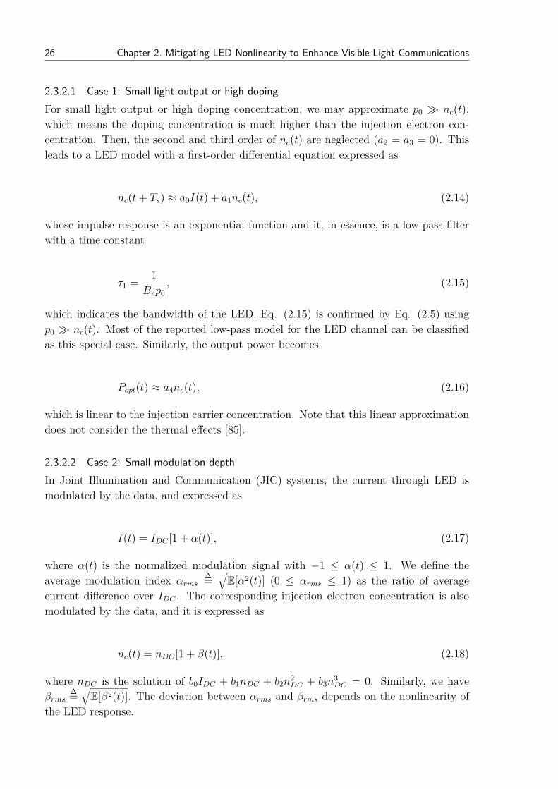
2.3.2.1 Case 1: Small light output or high dopingFor small light output or high doping concentration, we may approximate p0 nc(t),which means the doping concentration is much higher than the injection electron con-centration. Then, the second and third order of nc(t) are neglected (a2 = a3 = 0). Thisleads to a LED model with a first-order differential equation expressed as
nc(t+ Ts) ≈ a0I(t) + a1nc(t), (2.14)
whose impulse response is an exponential function and it, in essence, is a low-pass filterwith a time constant
τ1 = 1Brp0
, (2.15)
which indicates the bandwidth of the LED. Eq. (2.15) is confirmed by Eq. (2.5) usingp0 nc(t). Most of the reported low-pass model for the LED channel can be classifiedas this special case. Similarly, the output power becomes
Popt(t) ≈ a4nc(t), (2.16)
which is linear to the injection carrier concentration. Note that this linear approximationdoes not consider the thermal effects [85].
2.3.2.2 Case 2: Small modulation depthIn Joint Illumination and Communication (JIC) systems, the current through LED ismodulated by the data, and expressed as
I(t) = IDC [1 + α(t)], (2.17)
where α(t) is the normalized modulation signal with −1 ≤ α(t) ≤ 1. We define theaverage modulation index αrms
∆=√E[α2(t)] (0 ≤ αrms ≤ 1) as the ratio of average
current difference over IDC . The corresponding injection electron concentration is alsomodulated by the data, and it is expressed as
nc(t) = nDC [1 + β(t)], (2.18)
where nDC is the solution of b0IDC + b1nDC + b2n2DC + b3n
3DC = 0. Similarly, we have
βrms∆=√E[β2(t)]. The deviation between αrms and βrms depends on the nonlinearity of
the LED response.

Part I. Throughput in Visible Light Communication using LED 27
Inserting Eq. (2.17) and (2.18) into (2.8), we have
dnc(t)dt
= b0I(t) + b1nc(t) + b2n2c(t) + b3n
3c(t)⇔
nDCdβ(t)dt
= b0IDC [1 + α(t)] + b1nDC [1 + β(t)] + b2n2DC [1 + β(t)]2 + b3n
3DC [1 + β(t)]3
= b0IDCα(t) + (b1nDC + 2b2n2DC + 3b2
3n3DC)β(t) + (b2n
2DC + 3b3n
3DC)β2(t) + b3n
3DCβ
3(t),
(2.19)
where b0 = 1/(qtwAw), b1 = −Brp0−Anr, b2 = −Br and b3 = −Cnr. Eq. (2.19) indicatesthat the LED transient response model becomes a dynamic third-order differential equa-tion varying with the average illumination level (nDC). For a small modulation depth,the terms with the second and third order of β(t) are neglected. Thus, Eq. (2.19) issimplified as
dβ(t)dt−(b1 + 2b2nDC + 3b2
3n2DC
)β (t) + b0IDC
nDCα(t) = 0, (2.20)
which is a first-order linear differential equation of modulation signal β(t). Thus, Eq.(2.20) can be also interpreted as a low-pass filter with a time constant given by
τ2 = 1−b1 − 2b2nDC − 3b2
3n2DC
= 1Brp0 + Anr + 2BrnDC + 3C2
nrn2DC
, (2.21)
which indicates similar conclusions drawn from Eq. (2.5), i.e., both a high carrier con-centration nDC and a high doping concentration p0 can lead to a small time constant intransient response. Besides, we have τ1 > τ2 from Eq. (2.15) and (2.21). This meansthat a larger bandwidth can be achieved with a small modulation depth, compared tothe bandwidth for a small light output with the same doping level. Similarly, the outputpower is expressed as
Popt(t) = b4[p0nDC [1 + β(t)] + n2
DC(1 + β(t))2]
≈ b4[p0nDC + n2
DC + (p0nDC + 2n2DC)β(t)
], (2.22)
where b4 = 〈Ep〉AwtwBr. As we can see, Popt(t) is biased by two constant componentsand it is linear to a small modulation signal β(t).
2.4 Overcome the LED nonlinearity
To combat the effect of LED nonlinearity on communication performance, either an equal-izer is applied in the receiver or a predistorter is used in the transmitter, as shown inFigure 2.3. In this section, we firstly explore the possibility of applying the traditionalequalization techniques to the signal distorted by LED transient response in the receiver.Then a novel non-linear predistortion method is proposed.

28 Chapter 2. Mitigating LED Nonlinearity to Enhance Visible Light Communications
+
noise
I(t)Equalizer
LED model Receiver
Predistorter
Transmitter
LED
Figure 2.3: Solutions to nonlinear LED response.
2.4.1 Decision feedback equalization
When the channel is band-limited, the signal transmission at a symbol rate equal to orexceeding the channel bandwidth introduces Inter Symbol Interference (ISI) among adja-cent symbols. Traditional techniques to reduce the ISI include the Maximum-LikelihoodSequence Estimation (MLSE), the adaptive linear equalizer and the adaptive Decision-Feedback Equalizer (DFE) [152]. For a linear channel, although the MLSE has the bestperformance, it needs the estimation of the channel statistical characteristics in advanceand sometimes it is impossible. Hence, we mainly explore the widely used adaptive linearequalizer and adaptive DFE.
For the Case 1 in Section 2.3 (B), based on Eq. (2.14) and (2.16), the output poweris rewritten as
Popt(t) = a0a4I(t− Ts) + a1Popt(t− Ts). (2.23)
The transfer function H(Z) from current to optical power expressed as a Z transformis
H(Z) = a0a4Z−1
1− a1Z−1 , (2.24)
where H(Z) is stable as it has only one pole, which is less than 1. The linear equaliza-tions such as the Zero-Forcing (ZF) equalizer and Minimum Mean Square Error (MMSE)equalizer, are theoretically the inverse of H(Z) with a Finite Impulse Response (FIR)structure. However, due to the delay in the numerator of Eq. (2.24), the inverse of H(Z)is non-causal and thus linear equalizations without an additional delay are incapable ofcompensating for the signal distortion. In particular, the linear equalization is not validfor the LED model with nonlinearity.
In this chapter, an adaptive DFE is considered and it is essentially based on the InfiniteImpulse Response (IIR) structure as shown in Figure 2.4, where wn are the tap coefficientsof the equalizer, L is the tap number in its feedforward section and (N − L) is the tapnumber in its feedback section. We can apply IIR approximation for the DFE whenthe DFE works at the direct decision mode and the decision is correct [120]. During theequalization process, wn is adaptively updated for Eq. (2.24) such that the ISI is reduced.In general, the DFE can equalize the distorted signal without as much noise enhancementas that in the linear equalizer, but it may have the error propagation problem when there

Part I. Throughput in Visible Light Communication using LED 29
w1
Input
Output
Ts Ts
+
w2
Ts
wL
Ts Ts Ts
wL+1wL+2wN
Decision
Error
WeightUpdate
Training
Figure 2.4: Structure of decision feedback equalization
InRLS W0 LMS
Out
Figure 2.5: Implementation of adaptive decision feedback equalization
are error bursts. However, the error bursts are unlikely in most of the communicationsystem, in particular, by using techniques such as interleaving and coding [120].
For our practical implementation of the adaptive DFE, the whole equalization processis depicted in Figure 2.5. Firstly, the Recursive Least Squares (RLS) algorithm is usedto acquire initial converged coefficients wn using the training sequence, although it has aslow convergence speed and needs many computational resource. Then, the Least MeanSquare (LMS) algorithm is used to speed up the data processing.
The adaptive DFE can be also applied to the Case 2. However, for the general casewith nonlinear components, our simulation shows that the DFE cannot effectively improvethe BER performance. An alternative is to use nonlinear Volterra DFE [171]. However,in Volterra DFE, the computational complexity is increased significantly for the nonlin-ear kernel coefficients and thus it results in slow convergence speed. Therefore, a novelpredistorter is proposed in next section.
2.4.2 Non-linear predistortion
Due to the limitations of traditional equalizers for the LED nonlinearity, a more effectivepredistorter is considered in the transmitter to avoid noise enhancement in the receiver.In Figure 2.2, the nonlinearity of LED comes from the quadratic and cubic parts. Toovercome these nonlinearities, a nonlinear predistorter is constructed to predistort thesignal. Eq. (2.8) is rewritten as
nc(t+ Ts) = a0I(t) + a1nc(t) + a2n2c(t) + a3n
3c(t). (2.25)
Then, the first predistorter1 can be constructed based on
I(t) = 1a0I(t)− a1
a0I(t− Ts)−
a2
a0I2(t− Ts)−
a3
a0I3(t− Ts). (2.26)

30 Chapter 2. Mitigating LED Nonlinearity to Enhance Visible Light Communications
a0n(t)
+
noise
LinearEqualizer
LED non-linear model Receiver
+
c1
c0
c2
Predistorter
1/H2 1/H1 H1H2
+
Ts
a2
a4
a1a5()2
+
()2
Ts
()2
+d0
d1
()1/2+
d2
I(t) Popt(t)
Low-passFilter
a3 ()1c3()1
Figure 2.6: Proposed non-linear predistorter for non-linear LED channel
Similarly, Eq. (2.6) is rewritten as
Popt(t) = a4n(t) + a5n2(t). (2.27)
Thus, the second predistorter2 is constructed using
n(t) =
√√√√n(t)a5
+ a24
4a25− a4
2a5. (2.28)
Both the linear low-pass effect and the nonlinearity of LED are compensated by thepredistorter. Theoretically, the predistorter can precisely shape the signal waveform toensure the output of the LED is identical to the ideal signal. Such predistorter exhibitsa predominant pre-emphasis effect to invert the low-pass nature of the LED. This haspractical disadvantages, for instance in the dynamic range of the amplifier and in con-trolling the LED modulation depth. A suitable approach can be to let the transmitterpreserve the band-limited character in the LED channel, while the system can rely onknown techniques to combat the ISI, e.g., linear or DFE for PAM, or OFDM, possiblyincluding adaptive bit loading per subcarrier. Figure 2.6 illustrates how a low-pass filtercan be placed in front of the predistorter to preserve the LED high frequency fall-off.Commonly used equalizers can be then be applied across this LED communication chan-nel, in which non-linearities have been removed by the predistorer. Specifically in Figure2.6, c0 · · · c3 and d0 · · · d2 can be derived from Eq. (2.26) and (2.28).
In particular, compared to LED nonlinear model in Figure 2.2, the first time delayis omitted in Figure 2.6. This is because this delay is already implicitly included in thepredistorter and it is used for signal compensation. Moreover, there is no time delayin the main path of the signal through the predistorter and LED model in Figure 2.6,which indicates that the overall response of the predistorter and LED model becomesmemoryless.

Part I. Throughput in Visible Light Communication using LED 31
2.5 Channel capacity of a linear low-pass channel
With the novel nonlinear predistorter, the bandwidth of the LED channel is limited bythe low-pass filter. Based on the 3-dB bandwidth of the low-pass filter, it is of interest toestimate the achievable data throughput in VLC, along with the key system parameterssuch as the received SNR. For high data rate, the low-pass filter should be adoptedaccording to the bandwidth of other components such as the Digital-to-Analog Converter(DAC) where the sampling rate could be several Giga symbols per second (Gsym/s).
We apply a first-order RC low-pass filter in front of the predistorter to represent thewhole optical IM/DD channel, as in Figure 2.6, and its the time response is expressed as
h(t) = 1RC
e−tRC u(t), (2.29)
where u(t), R and C are the step function, resistance and capacitance, respectively. Then,its Fourier transform function is
H(jω) = 11 + jωRC
. (2.30)
The gain of the low-pass filter is described by
|H(f)| = 1√1 +
(f
f3 dB
)2, (2.31)
where f3 dB = 1/ (2πRC) is the 3-dB bandwidth of the lower-pass filter. Theoreticalinvestigations on the Shannon capacity of a linear channel are usually based on the well-known water-filling method [28, 102, 104, 152]. For a first-order low-pass optical IM/DDchannel with Gaussian noise, a closed-form expression for the channel capacity is givenby [102]
Cchannel = f3 dB2
ln 2
3
√32SNR− arctan 3
√32SNR
, (2.32)
where SNR represents the received signal-to-noise ratio after the photodiode (PD).The channel capacity versus received SNR is shown in Figure 2.7. As we can see, the
channel capacity is a monotonically increasing function with the SNR. The achievabledata throughput can be approximately calculated based on the received SNR and the3-dB bandwidth of the lower-pass filter [102]. For instance, when the SNR is 20 dB,the capacity is around of 11.4f3 dB bps. In practice, other interferences such as thequantization noise in the DAC should be considered, which lead to a decreased SNRand thus a decreased channel capacity. Note that the channel capacity is also related tothe structure of the low-pass channel. A Gaussian low-pass channel has a lower channelcapacity than the first-order low-pass channel [102]. This also gives us the insight to buildthe low-pass filter.

32 Chapter 2. Mitigating LED Nonlinearity to Enhance Visible Light Communications
0 10 20 30 40 500
50
100
150
SNR (dB)
Nor
mal
ized
cha
nnel
cap
acity
(
C/f 3−
dB )
SNR=20, C/f3−dB
=11.4
Figure 2.7: Channel capability of a first-order low-pass channel
+a0-a4
Update
( )I n( )I n
( )c n
LED
0( )I n
PD
Figure 2.8: Non-linear parameters estimation
2.6 Non-linear parameters estimation
In most applications, the LED parameters such as the doping level are unknown or dependon the DC bias current and temperature. In this case, these parameters can be estimatedby conducting dedicated experiments in advance or by using a training sequence duringdata transmission. In this chapter, we consider the second option and the parameterestimation is achieved by applying a training sequence at the start of one data frame.
The general structure of the nonlinear parameter estimator is shown in Figure 2.8,where the current is used for comparison. To avoid any channel and receiver introducednonlinearity, we normally measure the current or voltage from the Photodiode (PD) tocapture the nonlinear behaviour in LED, for instance, the voltage is measured in [85].Compared to the traditional linear adaptive filter where a FIR structure is applied, thenonlinear estimator with a0 − a5 in Figure 2.7 is based on the proposed LED nonlinearmodel. Although we can apply the same structure to estimate both c0 − c3 and d0 − d2
directly, the updating algorithm would become more complex and lead slow convergencerate. Hence, in this chapter, we estimate a0− a5 first and then apply them to the predis-torter. Based on the least square criteria, the nonlinear estimator adaptively minimizes

Part I. Throughput in Visible Light Communication using LED 33
the cost function c(n) such that
a = arga
min[c(n)2
]= arg
amin
[N∑n=0|I0(n)− I(n)|2
], (2.33)
where a is the vector of a0 − a5. In our case, the minimization results in a nonlinearparameter estimation problem with known system structure, which can be solved byNelder-Mead simplex direct search. The Nelder-Mead simplex direct search is derivativefree and it was implemented numerically in Matlab [122].
2.7 Simulations and Validation
This section presents simulation results based on the proposed nonlinear LED model andnonlinear predistorter. Firstly, the convergence of the Euler’s method is simulated withdifferent sampling rates. Then, we show the effect of the LED nonlinearity on the signalwaveforms and BER performance in OOK and PAM-4 systems. Based on these twosystems, we investigate the effectiveness of the traditional adaptive DFE, the proposedpredistorter and the parameter estimation by simulations. In particular, the relatedparameters of LED used in the simulation are list in Table 2.1.
2.7.1 Convergence of Euler’s method
To investigate the effect of LED nonlinearity on communication performance numerically,we use the model from Section 2.2 as a realistic representation for the LED in simulations.The accuracy of the Euler’s method for the LED equation depends on the samplinginterval Ts in Eq. (2.9). Based on the parameters listed in Table 2.1, we compare thesimulation results with different sampling rates as shown in Figure 2.9.
As can be seen, when we apply 100 samples per symbol, the step response of the LEDmodel is converged and the further increase of the samples makes not any difference. In
Table 2.1: Parameters for the LED model
Parameter Interpretation Valueq Charge of Electron 1.6× 10⁻¹⁹
Anr SRH recombination coefficient 0Br Radiative recombination coefficient 1.6× 10⁻¹⁰No./s/cm3
Cnr Auger recombination coefficient 0tw Active layer thickness 30× 10−7cmAw Active layer area 0.0139cm2
p0 Doping concentration 2× 10¹⁷ No./cm3
Ep Energy of photon (650nm) 3.06× 10⁻¹⁹JTs Sampling period in simulation 1ns

34 Chapter 2. Mitigating LED Nonlinearity to Enhance Visible Light Communications
1 1.5 2 2.5 3
x 10−7
0
0.2
0.4
0.6
0.8
1
Time (s)
Nor
mal
ized
opt
ical
pow
er
Output power with 15 samples/symbolOutput power with 50 samples/symbolOutput power with 100 samples/symbolOutput power with 1000 samples/symbolTransmitted signal
Figure 2.9: Comparison for the simulated LED nonlinear response using different samplingrates, for OOK signal with symbol rate 10Msym/s.
our case, since the symbol rate is 10Msym/s in the simulation, the sampling rate (1/Ts)is 1 Gigabit Samples Per Second (GSPS). Unless otherwise stated, we use Ts = 1 ns inthis chapter. In particular, the accuracy of approximation using Euler’s method can beanalytically evaluated by using Taylor series [72], which is not performed in this chapter.
2.7.2 LED nonlinear effect on OOK system
An LED is usually driven by a DC current IDC for illumination. With an average currentequal to IDC , data transmission is achieved by modulating the current in a JIC system. Insuch case, the injection electron concentration changes with the input current, governed bythe rate equation in Eq. (2.1). Figure 2.10 shows the injection electron concentration fordifferent IDC compared with the doping concentration, where we use an OOK signal withαrms = 1 and a data rate of 10 Mbps. As we can see, the injection electron concentrationfor the high-level part of OOK signal with IDC = 0.5 A is much higher than the dopingconcentration. In such case, a strong nonlinearity in the LED leads to a different rise andfall time. For a small light output with IDC = 1 mA, the injection electron concentrationis much lower than the doping concentration which can be approximated by a linear filteras our special Case 1. In particular, the injection electron concentration does not fall tozero for OOK signal in both of the two cases.
The corresponding output optical signals of the LED are shown in Figure 2.11. A highinput current level results in a short radiative recombination lifetime and vice versa, asindicated by Eq. (2.5). This phenomenon was also reported in [171]. Although a shortlifetime can support higher data rate for a high input current, it has different rise and falltimes due to the nonlinearity which is hardly eliminated by traditional linear techniques.In particular, our linear approximation for small light output (IDC = 1 mA) agrees wellwith our simulation.

Part I. Throughput in Visible Light Communication using LED 35
0 0.2 0.4 0.6 0.8 1
x 10−6
1013
1014
1015
1016
1017
1018
1019
Time (s)
Inje
cted
car
rier
conc
entr
atio
n n
c(t)
IDC
= 0.5 A
IDC
= 0.001 A
Doping concentration p0
Figure 2.10: Injected electron concentration nc(t) for different current levels IDC .
0 0.2 0.4 0.6 0.8 1
x 10−6
0
0.5
1
1.5
Time (s)
Nor
mal
ized
opt
ical
pow
er
Transmitted signalOutput signal with I
DC = 0.5 A
Output signal with IDC
= 0.001 A
Small light output approximation
Figure 2.11: LED output optical power under different input current levels for OOK signalwith a symbol rate 10Msym/s.
As we expected, the BER performance of the OOK system with a high input currentis better than that of a low input one, as shown in Figure 2.12, where the receiver isimplemented with a matched filter but without equalization. Note that, this result doesnot imply that the system with the nonlinearity can achieve better BER, because thelinear response that leads the same rise and fall time, which can be compensated by alinear equalizer. Here we highlight that the different rise and down ramp of the OOKsignal affects the communication performance. To further increase data rate, the BERperformance is limited by the LED nonlinearity and the linear equalization fails to improvethe BER performance.

36 Chapter 2. Mitigating LED Nonlinearity to Enhance Visible Light Communications
0 2 4 6 8 10 1210
−5
10−4
10−3
10−2
10−1
100
Eb/No, dB
Bit
Err
or R
ate
Simulation with IDC
= 0.5 A
Simulation with IDC
= 0.001 A
Theory
Figure 2.12: BER performance under different input current levels for OOK signal with symbolrate 10Msym/s.
2.7.3 LED nonlinear effect on PAM-4 system
Due to the non-radiative recombination Rnr0, there is an efficiency droop for high inputcurrent levels in LEDs. Thus, the LED optical power waveform are distorted by thismemoryless nonlinearity for multi-level modulation, such as PAM-4. Without consideringthe efficiency droop (Rnr0 = 0), one may also wonder the nonlinearity of the squareoperator both in Eq. (2.6) and in the dynamic rate equation of Eq. (2.8) would leadamplitude distortion of a PAM-4 signal. However, as our stationary solution in Eq.(2.13) indicated, the steady level is linear with the input current when those two squareoperators combined, i.e., Popt (t) = 〈Ep〉
qIDC with 〈Ep〉/q ≈ 1.91 in visible light spectrum.
This is confirmed by simulation using a multi-level PAM-4 signal through the LED, asshown in Figure 2.13, where the symbol rate is 50Msym/s. As expected, the four opticalpower levels are equally separated, although rise and fall times differ. Moreover, the falltime is longer than the rise time which is similar to the OOK signal. To enhance the datarate, either more levels are specified in a PAM system or a waveform shaping is appliedto prevent signal distortion.
To investigate the Symbol Error Rate (SER) performance of the PAM-4 system, weuse direct sampling at the end of each symbol instead of the matched filter. We foundthat the matched filter based receiver takes integration of each received symbol and thusthe nonlinear effect is accumulated, which results in a worse SER performance. Theconstellation of the PAM-4 signal after direct sampling is shown in Figure 2.14. Dueto the LED transient nonlinearity, lower amplitudes have more distortion than higheramplitudes have. This is quite different from the static nonlinear signal distortion inducedby the decreased efficiency of the LED, where the high amplitude trends to have moredistortion due to the efficiency droop.
The SER performance is illustrated in Figure 2.15 for a symbol rate of 10 Msym/s

Part I. Throughput in Visible Light Communication using LED 37
0 0.5 1 1.5 2
x 10−7
0
0.2
0.4
0.6
0.8
1
1.2
Time (s)
Nor
mal
ized
opt
ical
pow
er
Input currentLED output
Figure 2.13: LED output optical power with nonlinear distortion for PAM-4 signal with symbolrate 50Msym/s.
0 0.2 0.4 0.6 0.8 1−0.6
−0.4
−0.2
0
0.2
0.4
Nor
mal
ized
pha
se
Normalized amplitude
Input signalLED output signal
Large range Small range
Figure 2.14: Constellation of the PAM-4 signal with nonlinear distortion and symbol rate50Msym/s.
and 50 Msym/s. In the simulation, an adaptive DFE is implemented in the receiver. Forthe training sequence in the DFE, we use the RLS algorithm with the forgetting factor of0.999 and the LMS with updating step of 0.0001. The number of feedforward and feedbackweights is specified with 40 and 20, respectively. Since the nonlinearity has significanteffect on the SER performance when the symbol rate is 50Msym/s, the DFE fails toequalize the severely distorted signal. In particular, due to the direct sampling whensymbol rate is 10 Msym/s, the nonlinearity has negligible effect on the SER performancewhile it still induces deterioration for OOK system that employs a matched filter.

38 Chapter 2. Mitigating LED Nonlinearity to Enhance Visible Light Communications
0 2 4 6 8 10 12 1410
−5
10−4
10−3
10−2
10−1
100
Eb/N
0 (dB)
Sym
bol E
rror
Rat
e
Theoretical SERSimulated SER with 10Msym/sSimulated SER with 50Msym/s
Figure 2.15: SER performance of the PAM-4 system with symbol rate 50Msym/s.
0 0.2 0.4 0.6 0.8 1
x 10−6
−1
−0.5
0
0.5
1
1.5
Time (s)
Nor
mal
ized
opt
ical
pow
er
Input signalPredistorter output signalLED output optical power
Figure 2.16: LED response with predistortion for OOK signal with symbol rate 50Msym/s.
2.7.4 Non-linear predistortion
Based the proposed predistorter in Eq. (2.26) and (2.28), the transmit signal is predis-torted before it is fed into the LED. The input signal is compared with the LED outputas shown in Figure 2.16, which shows that we can almost get undistorted signal outputby using the predistorter. These results indicate the effectiveness of the predistorter.
In particular, in Figure 2.16, the output of the predistorter for the OOK signal hasvery sharp peaks in both of the rise and fall edges, which are hardly achieved by thecircuit. Hence, as discussed in previous section, a low-pass filter is necessary before thepredistorter and thus it preserves the linear low-pass property in practical channel. Inparticular, the predistorter is effective for the PAM-4 signal and any other modulationsignals.
Moreover, due to predistorted waveform with necessary peaks, there is a power penalty
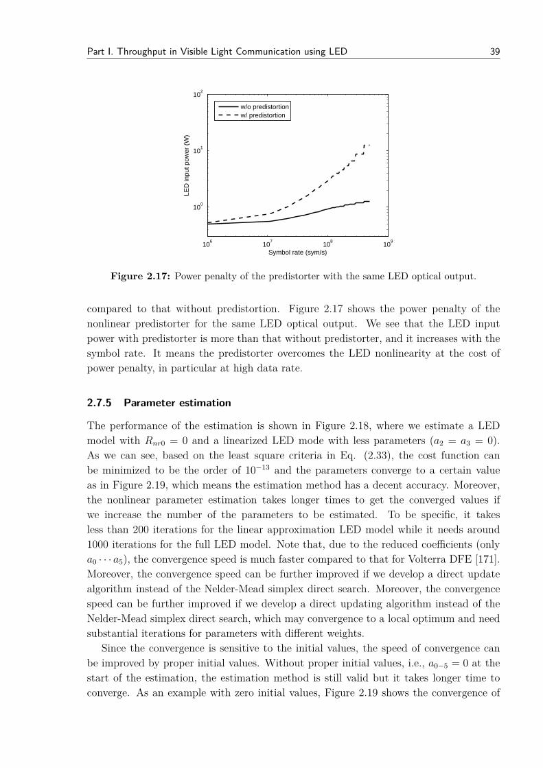
Part I. Throughput in Visible Light Communication using LED 39
106
107
108
109
100
101
102
Symbol rate (sym/s)
LED
inpu
t pow
er (
W)
w/o predistortionw/ predistortion
Figure 2.17: Power penalty of the predistorter with the same LED optical output.
compared to that without predistortion. Figure 2.17 shows the power penalty of thenonlinear predistorter for the same LED optical output. We see that the LED inputpower with predistorter is more than that without predistorter, and it increases with thesymbol rate. It means the predistorter overcomes the LED nonlinearity at the cost ofpower penalty, in particular at high data rate.
2.7.5 Parameter estimation
The performance of the estimation is shown in Figure 2.18, where we estimate a LEDmodel with Rnr0 = 0 and a linearized LED mode with less parameters (a2 = a3 = 0).As we can see, based on the least square criteria in Eq. (2.33), the cost function canbe minimized to be the order of 10−13 and the parameters converge to a certain valueas in Figure 2.19, which means the estimation method has a decent accuracy. Moreover,the nonlinear parameter estimation takes longer times to get the converged values ifwe increase the number of the parameters to be estimated. To be specific, it takesless than 200 iterations for the linear approximation LED model while it needs around1000 iterations for the full LED model. Note that, due to the reduced coefficients (onlya0 · · · a5), the convergence speed is much faster compared to that for Volterra DFE [171].Moreover, the convergence speed can be further improved if we develop a direct updatealgorithm instead of the Nelder-Mead simplex direct search. Moreover, the convergencespeed can be further improved if we develop a direct updating algorithm instead of theNelder-Mead simplex direct search, which may convergence to a local optimum and needsubstantial iterations for parameters with different weights.
Since the convergence is sensitive to the initial values, the speed of convergence canbe improved by proper initial values. Without proper initial values, i.e., a0−5 = 0 at thestart of the estimation, the estimation method is still valid but it takes longer time toconverge. As an example with zero initial values, Figure 2.19 shows the convergence of

40 Chapter 2. Mitigating LED Nonlinearity to Enhance Visible Light Communications
0 200 400 600 800 1000 120010
−15
10−10
10−5
100
105
Iteration
Cos
t fun
ctio
n va
lue
Approximated linear LED modelNon−linear LED model
Figure 2.18: Cost function values and iterations for parameter estimation.
0 50 100 150 200 250 300 350 400−2
0
2
4
6
8
10
Iteration
Nor
mal
ized
par
amet
er v
alue
s
Estimated a0
Estimated a1
Estimated a4
Ideal a0
Ideal a1
Ideal a4
Figure 2.19: Convergence and iterations of each parameter in a linear LED model.
the three parameters (a0, a1 and a4) in the approximated linear LED. In this case, theestimation takes more than 200 iterations before it reaches the optimal values.
The final estimated parameter values for the linear approximation LED and full non-linear LED are listed in the Table 2.2. In the estimation process, we applied normalizationto the parameters such that the dynamic range is significantly reduced. For instance, toestimate a0, we normalize a0 by 1017. This is because we already know several constants inadvance, including Ts = 10−9, q = 1.6× 10⁻¹⁹ and the LED technology (tw) in nanoscalewith 10−7 cm, thus we have Ts/(qtw) = 1017/1.6, which is a part of a0. From Table 2.2,we notice some mismatches between the objective values and the estimated values in bothof the two cases. This is because the global optimum is never reached within a limitednumber of iterations. Noticeably, the parameter a1 is identical to its real value, which isexpected to act as an important weight in our proposed LED model. In particular, the

Part I. Throughput in Visible Light Communication using LED 41
Table 2.2: Estimated parameters for the LED model (Normalized)
Parameter Objective values Estimated valuesfor linearized LED
Estimated valuesfor nonlinear LED
a0 × 1017 1.5 1.7653 1.888a1 0.98 0.98 0.98a2 × 10−19 −1 0 −0.7942a3 0 0 0a4 × 10−19 2.5485 2.1655 2.0239a5 × 10−36 1.2742 0 0.8037
Figure 2.20: Eye diagrams of PAM-4 signal with square-root raised cosine waveform shaping,symbol rate of 50 Msym/s and 30 dB SNR. (a) without predistortion; (b) with predistortion.
parameter discrepancy can be caused by other physical processes in practice which arenot considered in this chapter, e.g., the carrier leakage from active region to the barriers.Thus, our model is robust enough to cover the effect of those physical processes since itcan adaptively adjust a0 − a5.
To validate the proposed estimation approach and predistorter, we take following steps.Initially, based on the estimated parameters listed in the Table 2.2, the estimated LEDoutputs are compared with the objective outputs based the LED model. As we expected,the estimated output overlaps with the objective outputs, which means a great matchin between and it validates the proposed estimation approach. Secondly, based on theseestimated values, the predistorter is updated according to the proposed structure. TheLED output with predistortion correctly represents the input signal without noticeabledistortion. Thirdly, we apply the predistortion using estimated parameters in the PAM-4system, and simulation results shows that the eye diagram is significantly improved bythe proposed predistorter, as shown in Figure 2.20, where the symbol rate is 50 Msym/sand SNR is 30 dB. Note that this improvement cannot be achieved by using traditionalequalizers and predistorters based the LED models in Figure 2.1 (a-c). Finally, we applythis estimated predistorter for other SNRs and symbol rates, we see a dramatically im-proved SER performance even when the symbol rate increased to 500 Msym/s, as shownin Figure 2.21. We believe that the symbol rate can be further increased by the proposedapproaches.

42 Chapter 2. Mitigating LED Nonlinearity to Enhance Visible Light Communications
0 2 4 6 8 10 12 1410
−7
10−6
10−5
10−4
10−3
10−2
10−1
100
Eb/N
0 (dB)
Sym
bol E
rror
Rat
e
Theoretical SERSimulated SER w/o preditortion: 50Msym/sSimulated SER with estimated preditortion: 50Msym/sSimulated SER w/o preditortion: 500Msym/sSimulated SER with estimated preditortion: 500Msym/s
Figure 2.21: SER of the PAM-4 system with predistortion and estimation.
2.7.6 LED nonlinearity and non-linear predistortion in OFDM system
This section further investigates the LED nonlinearity and the non-linear predistorter va-lidity on the DC-biased optical OFDM (DCO-OFDM) system with continuous waveforms.Since the OFDM is not included in the standard IEEE 802.15.7 for VLC, the simulationconfiguration of OFDM is adapted from the IEEE 802.15.3a/802.11g, where QPSK andQAM are used. In the simulation, the frame period of the DCO-OFDM OFDM signalmeets Tframe = (2N +NCP )/fs, where N is the number of subcarrier, NCP is the numberof cyclic prefix points, and fs is also the DAC sampling rate for an IFFT size of 2N .Note that, to achieve a real-valued OFDM signal, a 2N -point IFFT is necessary followingthe Hermitian symmetry property [102]. Thus, Tframe increases with the the number ofsubcarrier N for a fixed sample rate Ts.
We present the OFDM spectrum with and without the predistorter, as shown in Figure2.22, where we see a significant out-of-band reduction by using the proposed nonlinearpredistorter. The out-of-band frequency leakage is mainly caused by the LED nonlin-earity. Moreover, due to the LED low-pass property, the high-frequency components ofOFDM signal are severely attenuated.
Since the spectrum has no phase information, Figure 2.23 further shows the constel-lation diagrams of 64-QAM OFDM signal with 30 dB SNR, where we reduce fs to 200Msym/s for a clear distortion pattern. Without the predistortion, the constellation dia-gram is largely distorted by the LED. Moreover, compared to the reported constellationdiagram with Wiener model in [153], we shows a different distorted constellation whilethe eye diagrams are also different by using Wiener model (see Figure 1(c) and (e)). Afterusing the predistorter, we see an improved constellation, which means the predistorter canreduce the out-of-band spectrum as well as minimize the in-band distortion for widebandOFDM signal. This is further confirmed by investigating the BER performance.
To this point, we verified that we can numerically estimate the LED parameters and
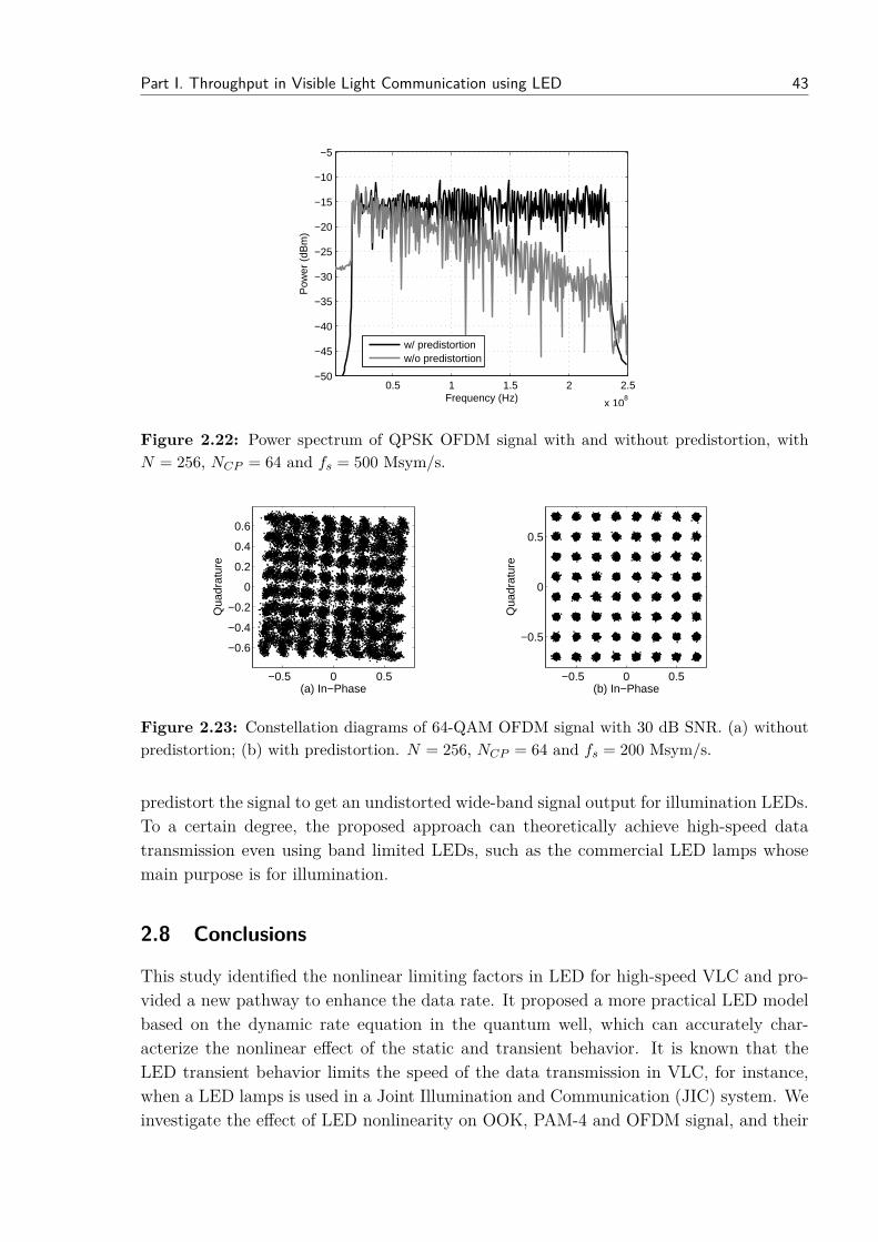
Part I. Throughput in Visible Light Communication using LED 43
0.5 1 1.5 2 2.5
x 108
−50
−45
−40
−35
−30
−25
−20
−15
−10
−5
Frequency (Hz)
Pow
er (
dBm
)
w/ predistortionw/o predistortion
Figure 2.22: Power spectrum of QPSK OFDM signal with and without predistortion, withN = 256, NCP = 64 and fs = 500 Msym/s.
−0.5 0 0.5
−0.6
−0.4
−0.2
0
0.2
0.4
0.6
Qua
drat
ure
(a) In−Phase
−0.5 0 0.5
−0.5
0
0.5
Qua
drat
ure
(b) In−Phase
Figure 2.23: Constellation diagrams of 64-QAM OFDM signal with 30 dB SNR. (a) withoutpredistortion; (b) with predistortion. N = 256, NCP = 64 and fs = 200 Msym/s.
predistort the signal to get an undistorted wide-band signal output for illumination LEDs.To a certain degree, the proposed approach can theoretically achieve high-speed datatransmission even using band limited LEDs, such as the commercial LED lamps whosemain purpose is for illumination.
2.8 Conclusions
This study identified the nonlinear limiting factors in LED for high-speed VLC and pro-vided a new pathway to enhance the data rate. It proposed a more practical LED modelbased on the dynamic rate equation in the quantum well, which can accurately char-acterize the nonlinear effect of the static and transient behavior. It is known that theLED transient behavior limits the speed of the data transmission in VLC, for instance,when a LED lamps is used in a Joint Illumination and Communication (JIC) system. Weinvestigate the effect of LED nonlinearity on OOK, PAM-4 and OFDM signal, and their

44 Chapter 2. Mitigating LED Nonlinearity to Enhance Visible Light Communications
related BER/SER and constellation performance deterioration. We show that the tradi-tional linear equalizer fails to recover the signal distorted by the nonlinear LED responseand the nonlinear Decision Feedback Equalizer (DFE) can only effectively work when thesignal is not severely distorted. A novel nonlinear predistorter is proposed based on thenonlinear LED model and it is validated by simulation. For any other LEDs where theparameters are unknown, the nonlinear parameter estimation method is proposed basedon the lease-square criteria. The estimation performance is investigated in terms of re-quired number of iterations and the achieved value of cost function, which indicates thatthe predistorter is attractive for implementation. Finally, the proposed predistorter hasbeen tested including the parameter estimation, which further validates the effectivenessof the nonlinear estimator. It is expected that the proposed methods can be used forhigh-speed VLC using traditional LED lamp where the bandwidth is limited.

Part II: Power Consumption in VisibleLight Communication Adopting LED
Lighting


CHAPTER 3
Modelling and Analysis of Transmitter Performance forHigh-Speed Visible Light Communications
This chapter is adapted from: X. Deng and J. P. M. G. Linnartz, ”Model of extra power inthe transmitter for high-speed visible light communication,” Communications and VehicularTechnology in the Benelux (SCVT), 2016 IEEE Symposium on, Mons, Belgium, 2016, pp. 1-6.c©IEEE
And from: X. Deng, Kumar Arulandu, Shokoufeh Mardanikorani, Yan Wu and J. P. M. G.Linnartz, ”Modelling and Analysis of Transmitter Performance for High-Speed Visible LightCommunications,” under review, IEEE Transactions on Vehicular Technology 2018. c©IEEE
Abstract –This chapter addresses the power penalty in a Visible Light Communica-tion (VLC) emitter that re-uses illumination Light Emitting Diodes (LEDs) for high-speed communications. We quantify the effect of modulation depth for two widely ex-plored modulation schemes in VLC, namely Orthogonal Frequency Division Multiplexing(OFDM) and Pulse Amplitude Modulation (PAM). Extra power is dissipated in the LEDand in the modulator due to such modulation. Two popular high-speed VLC transmittertopologies, namely a Bias Tee (Bias-T) and a Serial FET (Serial-F), are compared interms of efficiency, Extra Energy Per Symbol/Bit (EEPS/B) and complexity. This workpresents a theoretical model and compares it to simulation results. We show that 2-PAMoutperforms OFDM in terms of better Bit Error Rate (BER), larger dynamic range formodulation depth, less extra power loss, thus higher power efficiency for communication.
3.1 Introduction
Emerging Visible Light Communication (VLC) has gained much interest for indoor wire-less communications due to the extensive employment of Light Emitting Diodes (LEDs)for illumination. VLC offers a number of unique advantages over Radio Frequency (RF)
47

48 Chapter 3. Modelling and Analysis for Transmitter Performance in Visible Light...
Table 3.1: Summary of JIC transmitter performance in literatures
Ref. Year Core Technology Efficiency Data rate Modulation[129][128]2017 Buck Discrete components 40-88.6% 2Mbps VPPM[23]2016 Boost 0.35µm CMOS 85-92% 266Kbps OOK[57]2016 Buck Discrete components 80.8% 1Mbps VPPM[77]2015 Class AB 0.18µm CMOS 67% 500Mbps OFDM[126]2014 Buck 0.18µm CMOS 89% 2.5-7Mbps OOK/VPPM
communication, such as unregulated bandwidth for high data rate, a high degree of spatialreuse [178], secure connectivity, absence of electromagnetic interference and the potentialcombination with existing lighting [54, 81]. In Joint Illumination and Communication(JIC) systems, the transmitter is preferably uses a standard LED DC power driver withadditional components for modulation, for instance by separately injecting an AC modu-lating current [29, 88] or by regulating the entire DC and AC LED current [33, 35, 108].Several modulation schemes have been proposed for JIC systems. For high data rates, sig-nificantly above the flat pass-through band of the LEDs, multi-carrier approaches such asOrthogonal Frequency Division Multiplexing (OFDM) have been investigated extensively,e.g. in [45, 133]. At lower rates, sequential transmission of symbols at baseband is morepopular such as On-Off Keying (OOK), Variable Pulse Position Modulation (VPPM) andColor-Shift Keying (CSK), which are recommended in the IEEE standard 802.15.7 [2]. Toaccommodate dimming, a Pulse-Width Modulation (PWM) was proposed in [113, 114]with a variable duty cycle.
VLC is considered to be a green technology since it modulates the current throughexisting illumination LEDs and reuses the illumination power for communication [81, 94].Yet, there is a power penalty associated with operating LEDs at rapidly varying powerlevels for data modulations. For instance, a Field Effect Transistor (FET) modulator inseries with the LED consumes extra power [33, 35]. The loss in the LED itself was ana-lyzed in [38, 112, 177]. The power penalty further depends on the modulation method, inparticular on the probability density of the data signal amplitude. For instance, althoughOFDM can increase the ability to exploit a higher LED bandwidth, its large dynamicrange introduces significant extra energy loss compared with some other modulationmethods [112]. A power consumption factor, i.e., the maximum number of transmit-ted bits per Joule, is used to analyze the performance in VLC systems [177], which wasoriginally used for comparing the power efficiency of conventional communication systemsand networks [135]. The power penalty in different VLC emitters for the Binary PhaseModulation (BPM) was reported in [34]. This chapter further quantifies the extra powerconsumption and Bit Error Rate (BER) associated with 2-level Pulse Amplitude Mod-ulation (2-PAM or DC-biased OOK) and with OFDM modulation, considering suitablehigh-speed electronic circuit topologies.
Several topologies are used for LED DC drivers, including current mirrors, linearregulators, and Switched Mode Power Supplies (SMPSs) [186]. Due to the high power

Part II. Power Consumption in Visible Light Communication Adopting LED Lighting 49
LED
Modulator
V1(t)
V2(t) M
I1(t)
I2(t)
VinPower
Supply
Vb
Ib
Figure 3.1: Transmitter with serial modulator for VLC.
efficiency and ease of digital control, SMPSs are dominantly used in the lighting industryand efficiencies of around 90% are common [119]. Popular examples of SMPSs are thebasic buck, boost, Cuk and fly-back converter, depending on the application [186]. Basedon these LED drivers, the JIC transmitters add data transmission. Table 3.1 summarizesthe performance of published JIC transmitters using conventional drivers, including theeffect of different dimming levels required by the illumination function. It appears thatmany reported JIC transmitters are optimized for a specific modulation type, e.g., eitherhard VPPM or OOK switching but or for contunuous waveforms as in OFDM. Moreover,the creation of a high-speed and efficient transmitters that accommodate the high Peak-to-Average Power Ratio (PAPR) of OFDM, has been acknowledged as a key challenge forJIC OFDM systems [112].
If the symbol rate is at least an order of magnitude below the switching frequency insidethe SMPS driver, one can directly modulate the current through the control-loop(s) ofthe LED driver for switched modulations [37] and the Quadrature Amplitude Modulation(QAM) [160], with high power efficiency. However, the data rate is restricted by theoptimized control signal [34], by considering the speed and switching losses.
To support high data rates without restrictions on the SMPS, an additional modulatorcan be used either in parallel with LED (as a shunt) [65, 127, 129] or in series with theLED [33, 35, 108]. In particular, a parallel switch is only suitable for on-off modulationsuch as OOK but is not power efficient [37]. Towards high speed and high efficiency, thischapter focusses on a serial modulator. As shown in Figure 3.1, the power supply can bean SMPS and the modulator can be implemented as a Bias Tee (Bias-T) or a Serial FET(Serial-F). Moreover, the circuit in Figure 3.1 can support discrete and continuous typesof modulation.
The contributions of the chapter are outlined as follows. Section 3.2 quantifies theextra power dissipated in the LED due to modulation. Section 3.3 compares the Bias-Tand Serial-F topologies in terms of energy efficiency, proposed Extra Energy Per Symbol(EEPS), their suitability for discrete (binary or multilevel) and continuous modulationmethods, the complexity and cost of realization. The transmit power efficiency is ad-dressed in Section 3.4 for a typical SMPS. Section 3.5 presents the communication perfor-mance in terms of received energy per symbol, channel capacity and BER, as a function
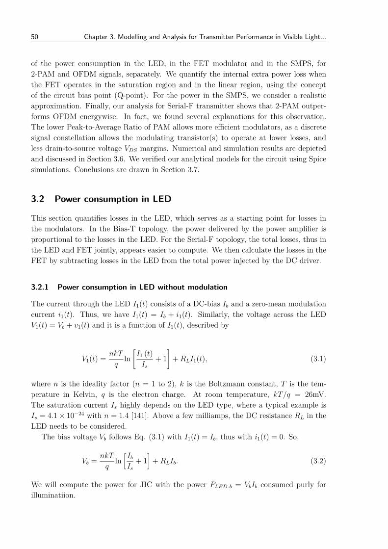
50 Chapter 3. Modelling and Analysis for Transmitter Performance in Visible Light...
of the power consumption in the LED, in the FET modulator and in the SMPS, for2-PAM and OFDM signals, separately. We quantify the internal extra power loss whenthe FET operates in the saturation region and in the linear region, using the conceptof the circuit bias point (Q-point). For the power in the SMPS, we consider a realisticapproximation. Finally, our analysis for Serial-F transmitter shows that 2-PAM outper-forms OFDM energywise. In fact, we found several explanations for this observation.The lower Peak-to-Average Ratio of PAM allows more efficient modulators, as a discretesignal constellation allows the modulating transistor(s) to operate at lower losses, andless drain-to-source voltage VDS margins. Numerical and simulation results are depictedand discussed in Section 3.6. We verified our analytical models for the circuit using Spicesimulations. Conclusions are drawn in Section 3.7.
3.2 Power consumption in LED
This section quantifies losses in the LED, which serves as a starting point for losses inthe modulators. In the Bias-T topology, the power delivered by the power amplifier isproportional to the losses in the LED. For the Serial-F topology, the total losses, thus inthe LED and FET jointly, appears easier to compute. We then calculate the losses in theFET by subtracting losses in the LED from the total power injected by the DC driver.
3.2.1 Power consumption in LED without modulation
The current through the LED I1(t) consists of a DC-bias Ib and a zero-mean modulationcurrent i1(t). Thus, we have I1(t) = Ib + i1(t). Similarly, the voltage across the LEDV1(t) = Vb + v1(t) and it is a function of I1(t), described by
V1(t) = nkT
qln[I1 (t)Is
+ 1]
+RLI1(t), (3.1)
where n is the ideality factor (n = 1 to 2), k is the Boltzmann constant, T is the tem-perature in Kelvin, q is the electron charge. At room temperature, kT/q = 26mV.The saturation current Is highly depends on the LED type, where a typical example isIs = 4.1× 10⁻²⁴ with n = 1.4 [141]. Above a few milliamps, the DC resistance RL in theLED needs to be considered.
The bias voltage Vb follows Eq. (3.1) with I1(t) = Ib, thus with i1(t) = 0. So,
Vb = nkT
qln[IbIs
+ 1]
+RLIb. (3.2)
We will compute the power for JIC with the power PLED b = VbIb consumed purly forilluminatiion.

Part II. Power Consumption in Visible Light Communication Adopting LED Lighting 51
3.2.2 Extra power consumption in LED for modulation
If the LED is modulated by a stationary and ergodic random signal, its power consumptionPLED can be calculated by the expectation
PLED = E [V1(t)I1(t)]
=∫ ∞
0
nkT
qI1 ln
[I1
Is+ 1
]+RLI
21
f(I1)dI1
, (3.3)
where f(I1) is the probability density function of the modulated current I1(t).The modulated current is also expressed as I1(t) = [1 + α(t)] Ib, where the modulation
α(t) is normalized to the LED DC current Ib with −1 ≤ α(t) ≤ 1 and E [α(t)] = 0.Thus, we have i1(t) = α(t)Ib. We define the root-mean-square modulation index αrms ∆=√E[α2(t)] (0 ≤ αrms ≤ 1) which equals the square root of the ratio of the AC power
over the DC power. For OFDM with a sufficiently large number of sub-carriers, α(t) canbe well approximated as a Gaussian random signal [9], i.e., α(t) ∼ N (0, α2
rms), whereusually αrms < 0.3 to avoid significant clipping distortions. Thus, after DC-biased opticalOFDM (DCO-OFDM) modulation, we have I1(t) ∼ N (Ib, α2
rmsI2b ). For a 2-PAM signal,
α(t) ∈ −αrms, αrms thus with two discrete values. As a special case, for unbiasedOOK, αrms = 1.
Inserting I1(t) = [1 + α(t)] Ib into Eq. (3.3) and subtracting the DC power in Eq.(3.2), the extra power consumed by the LED is
∆PLED = nkT
qIbE
[[1 + α(t)] ln
[1 + α(t)Ib
Ib + Is
]]+RLI
2bE[a2(t)
]≈ nkT
qIbE [[1 + α(t)] ln [1 + α(t)]] +RLI
2b a
2rms
, (3.4)
since the saturation current Is Ib. With −1 ≤ α(t) ≤ 1, the Taylor series expansion ofln [1 + α(t)] follows
ln [1 + α(t)] =∞∑m=0
(−1)mαm+1(t)m+ 1
= α(t)− α2(t)2 + α3(t)
3 − α4(t)4 · · ·
. (3.5)
Inserting Eq. (3.5) into (3.4), extra power in the LED is
∆PLED ≈nkTIbq
E[ ∞∑m=0
(−1)m[αm+1(t) + αm+2(t)
]m+ 1
]+RLI
2b a
2rms
≈ nkTIbq
E[α(t) + α2(t)
2 − α3(t)6 + α4(t)
12 · · ·]
+RLI2b a
2rms
. (3.6)

52 Chapter 3. Modelling and Analysis for Transmitter Performance in Visible Light...
1 1.5 2 2.5 3 3.5 40
100
200
300
400
500
600
700
800
Voltage (V)
Cur
rent
(m
A)
Diode equationApproximation
Ib = 350mA
Figure 3.2: A typical LED V-I curve
From Eq. (3.6), we conclude that ∆PLED depends on the statistical properties of themodulation α(t), in particular, on the moments E [αm(t)]. The extra power loss in thelinear resistance RL only depends on the second moment while the extra power loss inthe nonlinear component depends also on higher-order moments. For a small modulationindex, we use ln [1 + α(t)] ≈ α(t), so Eq. (3.4) is well approximated by
∆PLED ≈ a2rms
(nkT
qIb +RLI
2b
). (3.7)
In essence, this approximation is equal to modelling the LED junction as the dynamicresistance with, for Is Ib,
RDyn(Ib) = dV (I1)dI1
∣∣∣∣∣I1=Ib
= nkT
qIb+RL. (3.8)
To express the power consumption, the diode equation in Eq. (3.1) can be linearizedas [38]
V1(t) ≈ nkT
qln[IbIs
+ 1]
+RLIb +RDyn(Ib)Ibα(t). (3.9)
Figure 3.2 confirms that for a small modulation in current, the linearization is rea-sionable.
When the LED is modulated by a DCO-OFDM signal, the extra power in the LEDis calculated by inserting a Gaussian distribution I1(t) ∼ N (Ib, α2
rmsI2b ) into Eq. (3.3)
and it is approximated by Eq. (3.7) for a small αrms. For binary modulation with[1− αrms, 1 + αrms]Ib, not necessarily with small depth, and equal probability, the extra

Part II. Power Consumption in Visible Light Communication Adopting LED Lighting 53
power in the LED is [112]
∆PLED D = 12nkT
qIb(1 + αrms) ln
[Ib(1 + αrms)
Is+ 1
]+ 1
2nkT
qIb(1− αrms) ln
[Ib(1− αrms)
Is+ 1
]+ 1
2RL(1 + αrms)2I2b + 1
2RL(1− αrms)2I2b − PLED b
= nkT
qIb ·B +RLI
2bα
2rms
, (3.10)
where we introduce the constant
B = 1− αrms2 ln (1− αrms) + 1 + αrms
2 ln (1 + αrms) . (3.11)
For small αrms, B → 1. Yet, for OOK (αrms = 1), using lim x ln x = 0 for x→ 0, thefactor B → ln 2.
3.3 Power consumption in modulator
The two popular topologies in Figure 3.3 mainly differ in whether the data modulator alsocarries the LED DC bias. The Bias-T, shown in Figure 3.3 (a), blocks the data signalfrom entering into the DC power source, but the Power Amplifier (PA) needs its ownsupply. In the Serial-F topology of Figure 3.3 (b), the FET needs a voltage margin toaccommodate the signal modulation, which extracts fully from the main DC LED supplyVbus [112]. Evidently, the power consumption in the LED itself does not depend on thedriver topology. The main difference of the power consumption in these two topologies isthe power loss in the PA of Figure 3.3 (a) and in the serial FET of Figure 3.3 (b).
The losses in the modulator depend on the square root of PAPR z, that is, z is the ratioof the peak modulation depth αpeak over the rms modulation depth αrms (z = αpeak/αrms).Typically, z = 3 for the DCO-OFDM signal with 3-sigma clipping, z =
√2 for a DCO-
BPSK modulated sinusoidal carrier and z = 1 for OOK or two-level Amplitude ShiftKeying (ASK).
3.3.1 Extra supply power in Bias-T transmitter
Through the Bias-T, the data source delivers extra power ∆PLED into the LED, via aPA [106]. Both the additional PA and the Bias-T introduce a power loss. We define theefficiency of the Bias-T solution, including the PA, as
ηPA−BT = ∆PLEDPBT
, (3.12)
where we take ∆PLED from (7) and where the extra supply power in Bias-T topology,PBT , mainly depends on its operating class [105], as shown in Figure 3.4.

54 Chapter 3. Modelling and Analysis for Transmitter Performance in Visible Light...
L
C Bias Tee
LED
Data
LED
Vswing+Vmin
(a) Bias-T based (b) Serial-F based
Vbus Vbus
PA
Data
Amplifier
GFET
D
S
Figure 3.3: Two common structures of transmitter for high-speed VLC.
Bias Tee
LED
(a) Class A amplifier
VA
C
LA
RA
RBTC
Vbus
L
RBTL
Vbias
vin
LED
VB
C RBTC
Vbus
L
vin
-VB
(b) Class B amplifier
Bias Tee
RBTL
Figure 3.4: Bias-T solution based on Class A and Class B amplifier.
3.3.1.1 Efficiency in Bias-T with Class A amplifierWe consider a Class A amplifier with a bias current IA to modulate the signal on the LEDcurrent. In Class A, IA equals the maximum deviation of the current though the LEDload. Thus IA = αpeakIb. The amplifier needs to drive this current into a load composedof the LED resistance plus the Equivalent Series Resistance (ESR) RBTC of the capacitorin Bias-T, so it sees a resistance
RBTC +RLED = RBTC +RDyn = RBTC + nkT/qIB +RL. (3.13)
The biasing inductor LA acts as a fixed current source, provided that for all rele-vant modulating frequencies jωLA >> RBTC + RLED. The required supply voltage isVA = αpeakIb [RBTC + nkT/(qIb) +RL +RA] +Vmin, where RA is the ESR of the PA biasinductor and Vmin is an additional minimum voltage to prevent distortion. That is, itconsumes
PA = α2peakI
2b [RBTC + nkT/(qIb) +RL +RA] + αpeakIbVmin. (3.14)
In the ESR RBTL of the inductance of the Bias-T, we see further losses
PBTL = RBTLI2b . (3.15)
Part II. Power Consumption in Visible Light Communication Adopting LED Lighting 55
The efficiency of the modulation in Bias-T with Class A is thus calculated by
ηA = ∆PLEDPA + PBTL
= α2rms(nkTIb/q +RLI
2b )
α2peakI
2b [RBTC + nkT/(qIb) +RL +RPA] + αpeakIbVmin +RBTLI2
b
. (3.16)
For an ideal PA bias inductor, an ideal Bias-T and FET, thus with RA = 0, RBTC = 0,RBTL = 0 and Vmin = 0, Eq. (3.16) is reduced to
ηA = α2rms
α2peak
= 1z2 . (3.17)
Alternatively, in a purely resistor bias, (LA = 0, RA >> jωLA), the efficiency ηA in(17) is reduced by a factor of about 2, since the required supply voltage is doubled.
3.3.1.2 Efficiency in Bias-T with Class B amplifierA dual-ended (two-transistor) Class B amplifier can achieve higher power efficiency thana Class A amplifier. The bias current is nearly zero if modulation is absent (if α(t) = 0).Each transistor in a dual-ended Class B amplifier needs a similar supply voltage as theClass A amplifier
VB = αpeakIb [RBTC + nkT/(qIb) +RL] + Vmin. (3.18)
Because of symmetry, the average current through the upper transistor in the activeperiod of the signal is calculated as Iavg = E[|α(t)Ib|]. Each supply delivers the samecurrent magnitude [58], so each transistor consumes PB = VBIavg/2 as it is only active50% of the time. We use this to express the efficiency of a Class B amplifier, as
ηB = ∆PLED2PB + PBTL
= α2rms(nkTIb/q +RLI
2b )
αpeakI2bE [|α(t)|] [RBTC + nkT/(qIb) +RL] + VminIbE [|α(t)|] +RBTLI2
b
. (3.19)
For a purely resistive load and an ideal Bias-T and FET, Eq. (3.19) becomes
ηB = α2rms
αpeakE [|α(t)|] = αrmszE [|α(t)|] , (3.20)
where E [|α(t)|] = 1 for OOK, E [|α(t)|] = 2αpeak/π for DCO-BPSK and E [|α(t)|] =αrms
√2/π for DCO-OFDM, respectively.

56 Chapter 3. Modelling and Analysis for Transmitter Performance in Visible Light...
3.3.2 Power consumption in Serial-F transmitter
The power consumption PM in the modulator is calculated by using the instantaneouscurrent I2(t) (which equals the LED current I1(t)) and the voltage V2(t) across the mod-ulator, thus
PM = E [V2(t)I2(t)] = E [V2(t)I1(t)] . (3.21)
Yet, it appears easier (see [112]) to calculate the extra power PSF = ∆PLED+PM thatthe main DC driver needs to deliver, with
PSF = E [V1(t)I1(t)] + E [V2(t)I1(t)]− VbIb. (3.22)
If the LED is biased by an ideal voltage source Vbus, V1(t) + V2(t) = Vbus is constant.Hence, PSF = VbusE [I1(t)]− VbIb = (Vbus− Vb)Ib. That is, in contrast to the situation fora Bias-T that creates a separate AC power equal to ∆PLED from a separate supply VAfor its PA, the Serial-F draws extra power from the LED DC supply Vbus.
The FET voltage V2(t) must be strictly positive. A proper design of the modu-lator needs to ensure that the FET controls its drain source voltage to achieve thedesired modulation, avoiding any FET specific distortion. So, conceptually we splitV2(t) into a FET-dependent part Vmin and an LED and modulation-dependent partV2(t) − Vmin = max [v1(t)] − v1(t) to accommodate the required variations v1(t) inthe LED voltage. So, during α(t) = αpeak, the FET voltage reaches its minimummin[V2(t)] = Vmin. By reducing it conductivity, the FET can control any (non-negative)lower current. During instances of α(t) = 0, a margin of V2(t) = Vmin + Vswing must bemaintained such that pulling down the FET can adequately support modulation of αpeak,so Vswing = αpeak (RLIb + nkT/q).
Since Vbus = Vmin + Vswing + Vb , the extra supply power can be calculated from
PSF = (Vswing + Vmin) Ib. (3.23)
This explains why the power (defined strictly as an average over the multiplication of avoltage and a current) can be calculated as a multiplication of averages, thereby invertingthe sequencce of mathematical operations.
The load line in Figure 3.5 shows the relation between drain-source voltage VDS, thusV2(t), versus the FET/LED current I1(t) = I2(t), as dictated by the diode equation (1).
3.3.2.1 Power loss in serial FET for continuous signalTo determine Vmin1 for a continuous signal, we elaborate on the FET characteristics. Tooperate in a desired mode, the FET needs a DC bias, which is known as Quiescent point(Q-point) [58]. At the Q-point, the FET is fed by a DC voltage and current where thesignal is superimposed, as shown in Figure 3.5. In fact, for the linear modulation ofcontinuous signals I2(t) = [1 + α(t)]Ib around the Q-point (where α(t) = 0), such thatthe FET stays in the saturation region for any α(t).

Part II. Power Consumption in Visible Light Communication Adopting LED Lighting 57
VDS
Vmin1
G MOSFET
D
S
Ib
Linear region Saturation region
ID
VDS=VGS -Vt
Vswing1
Load line
time
tim
e
Q points
VGS -Vt
Vswing1 + Vmin1
vgs(t)
Vmin2=VD_high
VD_low
(1+αm )Ib
(1-αm )Ib
Vb+Vswing2+Vmin2 Vb+Vswing1 + Vmin1
Vswing2+Vmin2
(1+αpeak )Ib
(1-αpeak )Ib
Discrete signal
Continuous signal
Figure 3.5: FET I-V curves and DC bias for different modulation methods.
That is, the transition point should not be crossed by I2(t) = (1+αpeak)Ib, as depictedby the red modulation signal in Figure 3.5. The FET acts as a nonlinear voltage-controlledresistor. At the transition between the regions,
I2(t) = 12k′
n
W
LV 2DS(t), (3.24)
where W , L are the gate width and gate length, respectively. A typical value of k′n is200µA/V2 for an n-channel FET [58]. At the transition, we also see that VDS = VGS−Vt.So we require that
Ib(1 + αpeak) <12k′
n
W
LV 2DS(t), (3.25)
where we optimistically assume that we can operate the FET exactly towards this bound-ary, although in practice it may be hard to set this point due to unknown parameters soa safety margin is preserved.
These expressions show that a minimum VDS needs to be maintained of
VDS(t) > Vmin1 =√
(1 + αpeak)IbA
, (3.26)
where we collapsed all FET properties into a constant A, with
A = 12k′
n
W
L. (3.27)
For comparison, we are also interested in the power dissipated in the FET. Due to theadditional voltage Vswing1 and Vmin1 for continuous signal, the constant voltage is liftedto Vbus = Vb + Vswing1 + Vmin1. Thus, the power dissipated in the FET is calculated by
∆PFET C = E [VD(t)I1(t)]= E [Vb + Vswing1 + Vmin1 − V1(t) I1(t)]
. (3.28)
58 Chapter 3. Modelling and Analysis for Transmitter Performance in Visible Light...
Inserting Eq. (3.2), (3.22) and (3.23) into (3.28), we have
∆PFET C = (Vswing1 + Vmin1) Ib −∆PLED C
≈
αpeak (nkTq
+RLIb
)+
√(1 + αpeak)Ib
A
Ib −∆PLED. (3.29)
In other words, modulation requires extra power into the LED as well as extra powerfor the operation of the FET. Yet the expression for the sum of these two powers, simply is(Vswing1 + Vmin1) Ib. The power lost in the FET alone, can be determined by subtracting∆PLED from (Vswing1 + Vmin1) Ib, as in Eq. (3.29).
3.3.2.2 Power loss in serial FET for discrete signalIn switched mode, the extra power in the FET includes the conduction loss and switchingloss. Since a positive 2-PAM signal has I1(t) ∈ (1 − αrms)Ib, (1 + αrms)Ib with equalprobability, the conduction loss is
Pcon = 12VD highIb(1 + αm) + 1
2VD lowIb(1− αm), (3.30)
where VD high, VD low are the drain voltage for high and low current, respectively. Foralternating ones and zeros, the switching loss is
Pswitch = αmVDropIbRs(tcr1 + tvf1 + tvr1 + tcf1), (3.31)
where VDrop is the drain voltage drop between two current levels calculated by VDrop =VD high − VD low. Rs is the data symbol rate. tcr1, tvf1, tcf1 and tvr1 are the currentrising time, the voltage falling time, the current falling time, and the voltage rising time,respectively. For a random, independent sequence of binary data symbols, the probabilitythat two consecutive bits are equal is 1/2 and switching only occurs if bit values differ.Hence, statistical switching power losses one half of (31).
For a symbol duration Ts (in the order of µs) much longer than the rise or fall timeconstant (in in the order of ns), our simulation confirms that the extra power loss in FETis mainly determined by the conduction loss in Eq. (3.30).
For a 2-PAM signal, one can reduce the power consumption by not placing bothconstellation points in the saturation region, but to allow (at least) one point in thelinear region. Yet, placing both points in the linear region would dramatically reducethe speed of the FET. As a reasonable compromise, we bias the FET at the boundarybetween linear and saturation region with current Ib. Based on the load line in Figure3.5, the FET works in the linear region for high current level (1 + αrms)Ib while it worksin the saturation region for low current level (1 − αrms)Ib. At this Q point for switched

Part II. Power Consumption in Visible Light Communication Adopting LED Lighting 59
mode, we have
Vswing2 + Vmin2 =√IbA, (3.32)
where Vswing2 and Vmin2 are the corresponding upswing and minimum voltage for 2-PAMsignal. Thus, the conduction loss becomes
Pcon = 12Ib(1 + αm) Vb + Vswing2 + Vmin2 −max [V1(t)]
+ 12Ib(1− αm) Vb + Vswing2 + Vmin2 −min [V1(t)]
= Ib
√IbA−∆PLED D
, (3.33)
where max [V1(t)] and min [V1(t)] are calculated by using the (1 + αrms)Ib and (1− αrms)Ibin the diode equation of Eq. (3.1), respectively. As we can see, the DC bias in the serialFET provides the LED with extra power but it also dissipates power.
3.3.3 Proposed metric of Extra Energy Per Symbol (EEPS)
Similar to a radio system, the signal power used in Signal-to-Noise Ratios (SNR) in mostprevious papers refers to the total signal power, which predominantly is a function of theillumination intensity. Yet, VLC modulates the light already used for illumination butdoes not introduce more light [10]. So, the additional power lost in electronic components,on top of the illumination power is a more appropriate measure [34]. Thus, we proposea new metric, called Extra Energy Per Symbol (EEPS), to describe the power penalty inthe JIC transmitter when a lighting system is adopted for communication. The EEPScan be derived from previous equations along with the symbol rate Rs, as
∆E = PextraRs
, (3.34)
where the extra power Pextra equals PBT for Bias-T transmitter or equals PSF for Serial-Ftransmitter.
3.3.4 Comparison between Bias-T and Serial-F transmitter
We compare these two transmitter topologies for the same ∆PLED into the LED. Thesupply power PBT and PSF are directly used for comparison. For an ideal Bias-T and FET,Table 3.2 lists the supply power for several widely used modulation methods, includingOOK, BPSK and OFDM.
From Table 3.2, the Bias-T transmitter needs the same extra supply power as theSerial-F one (PBT = PSF ) for OOK signal. However, we always have PBT < PSF both

60 Chapter 3. Modelling and Analysis for Transmitter Performance in Visible Light...
Table 3.2: Comparison between Bias-T and Serial-F transmitter (Vmin = 0)
CasesNormalized extra supply power for signal†
Power consumptionBias-T (PBT )Serial-F (PSF )
Class A Class BGeneral expression α2
peak αpeakE [|α(t)|] αpeak N/Aαrms = αpeak = 1
1 1 1 PBT = PSF(OOK?)αpeak =
√2αrms ≤ 1
α2peak 2α2
peak/π αpeak PBT < PSF(DCO-BPSK)αpeak = 3αrms ≤ 1
α2peak αpeakαrms
√2/π αpeak PBT < PSF(DCO-OFDM)
†Based on Eq. (3.12) and (3.22), the supply power for signal is normalized by (nkTIb/q+RLI2b ).
?We assume OOK signal went through the Bias-T without distortion.
for BPSK and OFDM signal. Moreover, the Class A amplifier needs more supply powerthan the Class B amplifier due to its lower power efficiency.
An advantage of the FET modulator is that it works as a linear amplifier and thus noadditional PA is needed. However, the series FET modulator requires a proper biasingand a controlled supply voltage to minimize power losses. While, the Bias-T transmitterhas the advantage of easy implementation in the lab and thus it is usually employed toquickly investigate VLC system performance. Many reported researches on high-speedOFDM JIC systems demonstrated transmitters with a Bias-T [27, 29, 88, 125]. However,there are some limitations for Bias-T transmitters:
(1) Due to the low input signal power from the Digital Analog Converter (DAC), oneor more additional PAs are required. This will lead to high cost, large size, and lowefficiency of the whole transmitter, restricting the use of JIC in practice [57, 106].
(2) The impedance of the Bias-T topology is usually higher than that of the dynamicresistance of the LED loads which has a penalty of the efficiency.
(3) The Bias-T transmitter, where an inductor is necessary, is hardly used in IntegratedCircuits (IC). Moreover, due to the additional amplifier in this topology, it becomescomplex in the IC design.
(4) The Bias-T transmitter is hardly used for very fast switching mode modulationmethods while the Serial-F based transmitter can be efficiently applied for those modu-lations. This is mainly due to the fact that the Serial-F transmitter can achieve shorttransient time in LED [22].
Compared with Bias-T transmitter, the Serial-F transmitter, which is suitable for VLCtransmitter integration, can provide compatibility with most of the modulation methods.

Part II. Power Consumption in Visible Light Communication Adopting LED Lighting 61
D
C
UC
S
G
Buck Driver Modulator
VLC
LED
String
PWM
D
f1
LM1
R
Vdc
ID(t)
CTRL
Vbus
M2
I1(t)
M3
VDS(t)
Figure 3.6: Proposed Serial-FET transmitter for VLC.
3.4 Losses in the SMPS for DC
In a Bias-T approach the power for the PA presumably needs to be delivered via adedicated SMPS, whereas in a Serial-F set-up, the main DC LED driver needs to outputa slightly higher voltage as described in Eq. (3.23) but can deliver the same current Ib asin illumination only. Hence the efficiency at which the power for the modulation can beextracted from the main power is different as well.
To quantify this, Figure 3.6 shows a circuit diagram of a popular and power-efficientBuck SMPS with synchronous rectification and a simplified Serial-F transmitter. Thedissipated electrical power E [PBuck(t)] contains two types of losses, namely switchinglosses and conduction losses [37]. Simulations confirm that the power loss in the driverPBuck, as a function of an average current Ib, can be approximated by [112]
PBuck ≈ c1I2b , (3.35)
where, in good approximation, the loss coefficient c1 = Rind +Ron1D+Ron3(1−D). D isthe duty cycle in the internal Pulse-Width Modulation (PWM) of the Buck driver. Rind,Ron1 and Ron3 are the DC resistance of inductor, switch M1 and switch M3, respectively.
This expression reveals that the average current is the key parameter in the SMPSlosses, while the output voltage, subject to Eq. (3.23) does not have a dominant effect.Hence the power used for modulation does not yield extra losses in the SMPS for aSerial-F design, but has a penalty for Bias-T case.
3.4.1 Transmitter power efficiency
For a JIC transmitter, we define the energy efficiency as the ratio of the power dissipatedby the LED to the total dissipated power. Thus, the transmitter power efficiency iscalculated by
η = E [PLED(t)]E [PLED(t)] + E [PM(t)] + PBuck
, (3.36)

62 Chapter 3. Modelling and Analysis for Transmitter Performance in Visible Light...
where E[.] are the expectation of the power dissipated in the LED, modulator and Buckdriver, respectively.
For the Serial-F topology, mains-to-LED-illumination-power efficiency η = E [PLED(t)]/ [PLED b + PSF + c1I
2b ], where PSF is given by Eq. (3.22).
Yet, for the Bias-T, an extra loss term of PBuck PA ≈ c1α2peakI
2b occurs to power the
PA, which needs to be added to the denominator of Eq. (3.36). So η = E [PLED(t)]/[PLED b + PBT + c1(1 + α2
peak)I2b
].
3.4.2 Summary for Serial-F transmitter
For comparison, Table 3.3 lists the key formulas for calculating the received energy persymbol, the (extra) power, efficiencies in 2-PAM and OFDM systems. Different definitionsof efficiency are presented to evaluate the effect of modulation methods through differentaspects. For instance, the JIC transmitter efficiency η3 is based on the definition inEq. (3.36). Illumination efficiency η1 is the ratio of the effective illumination powerover the total dissipated power. Communication efficiency η2 is the ratio of the effectivecommunication electrical power to the extra power loss. SMPS efficiency η4 is the ratioof the SMPS output power to its input power.
Theoretical bound for the efficiency in a 2-PAM or OFDM system can be derived ifwe assume the SMPS has an efficiency of η4 = 100% (P2 = 0) and the modulator islossless (∆P3 = 0). In this case, with αrms = 1, n = 1.4, RL = 5.5 Ohm and Ib = 0.35A in a typical mid-power LED, the efficiency of the transmitter becomes η1 = 66.3%,η2 = 100.6%, η3 = 100% for 2-PAM, and η1 = 66.2%, η2 = η3 = 100% for OFDM. Similarbounds can be derived for other modulation depths. As we can see, the theoreticalefficiency is modulation-dependent. The power loss in the SMPS and modulator furtherreduce the efficiency. Moreover, the communication efficiency η2 is more than 100%,which means that 2-PAM can reuse a part of energy that is used for illumination. Thisis also indicated by that the communication power can be larger than the extra power inLED (P4 > ∆P1) for 2-PAM. However, for a continuous waveform such as in OFDM, thecommunication power never exceeds the extra power in a LED (P4 ≤ ∆P1) which leadsto a theoretical communication efficiency η2 ≤ 100%. In practice, OFDM usually needsmore power in a linear FET modulator. As a consequence, it has a lower communicationefficiency compared to the 2-PAM.
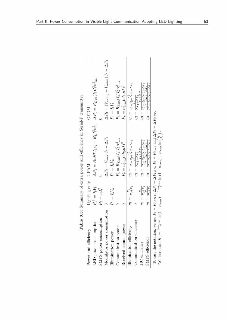
Part II. Power Consumption in Visible Light Communication Adopting LED Lighting 63
Tab
le3.
3:Su
mm
ary
ofex
tra
pow
eran
deffi
cien
cyin
Seria
l-Ftr
ansm
itter
Pow
eran
deffi
cien
cyLi
ghtin
gon
ly2-
PAM
OFD
MLE
Dpo
wer
cons
umpt
ion
P1†
=I bVb
∆P
1=BnkTI b/q
+RLI
2 bα
2 m∆P
1=RDyn(Ib)I
2 bα
2 rms
SMPS
pow
erco
nsum
ptio
nP
2=c 1I
2 b0
0M
odul
ator
pow
erco
nsum
ptio
n0
∆P
3=Vmin
1Ib−
∆P
1∆P
3=
(Vswing
+Vmin
2)I b−
∆P
1Ill
umin
atio
npo
wer
P1
=I bVb
P1
=I bVb
P1
=I bVb
Com
mun
icat
ion
pow
er0
P4
=RDyn(Ib)I
2 bα
2 rms
P4
=RDyn(Ib)I
2 bα
2 rms
Rec
eive
dco
mm
.po
wer
0Pr
=α
2 rms(εh
0µI)2
Pr
=α
2 rms(εh
0µI)2
Illum
inat
ion
effici
ency
η 1=
P1
P1+P
2η 1
=P
1P
1+P
2+
∆P
1+
∆P
3η 1
=P
1P
1+P
2+
∆P
1+
∆P
3
Com
mun
icat
ion
effici
ency
0η 2
=P
4∆P
1+
∆P
3η 2
=P
4∆P
1+
∆P
3
JIC
effici
ency
η 3=
P1
P1+P
2η 3
=P
1+
∆P
1P
1+P
2+
∆P
1+
∆P
3η 3
=P
1+
∆P
1P
1+P
2+
∆P
1+
∆P
3
SMPS
effici
ency
η 4=
P1
P1+P
2η 4
=P
1+
∆P
1+
∆P
3P
1+P
2+
∆P
1+
∆P
3η 4
=P
1+
∆P
1+
∆P
3P
1+P
2+
∆P
1+
∆P
3† T
oea
seth
eno
tatio
n,w
eus
eP
1=PLEDb,∆
P1
=∆PLED
,P2
=PBuck
and
∆P
3=
∆PFET
.?W
ein
trod
uceB
1=
1+α
rm
s
2ln
(1+αrms)−
1−α
rm
s
2ln
(1−αrms)+
αrms
ln( I b I s) .

64 Chapter 3. Modelling and Analysis for Transmitter Performance in Visible Light...
3.5 Communication performance
Energy per symbol (Es) is a well-used metric to evaluate the communication performance.In JIC systems, only a part of the transmitted optical power is effective for communica-tion. Therefore, we use the received Es after the propagation channel to investigate theeffective communication power for different modulation methods and it is determined bythe modulation index. The received Es along with the noise level forms ES/N0 which willbe used to calculate the capacity and BER in the receiver.
3.5.1 VLC Channel Model
Intensity Modulation and Direct Detection (IM/DD) over a wireless optical channel canbe modeled as a baseband linear system with an transmitted optical signal X(t) over achannel equivalent impulse response h(t), which leads to an received current r(t) with anadditive Gaussian noise n(t) [82, 83]. The received signal is expressed as
r(t) = εX(t)⊗ h(t) + n(t), (3.37)
where ε is the responsivity (A/W) of the PD. In particular, the low-pass responses inLED and in the phosphor are not addressed explicitly in the scope of this chapter.
The path from an LED to a photodetector (PD) is usually modeled as a flat fadingchannel with a fixed propagation delay and DC gain. Since the delay spread is aboutseveral nanoseconds (ns) within an indoor scenario [103], we only consider the DC gainin this work. Assuming a Lambertian radiation for LEDs, the DC gain is expressed as[51, 82]
h(t) = h0δ(t) = A(m+ 1)cosm(φ) cos θ2πd2 δ(t), (3.38)
where h0 denotes the optical channel DC gain and δ(t) is the impulse function. Tocalculate h0, A, φ, θ, d are the surface area of the PD, off-axis angle relating to thetransmission direction of the main band, off-axis angle relating to direction of PD, andthe distance between the lamp and detector, respectively. The order m is related to thesemi-angle via m = − ln 2
/ln(cos Φ1/2), where Φ1/2 is the semi-angle at half power of the
LEDs.The Gaussian noise n(t) includes the shot noise and thermal noise [161]. Since the
shot noise is signal-dependent, n(t) becomes signal-dependent and its Power SpectrumDensity (PSD) is given by
N0(t) = Nshot(t) +Nthermal = 2qεPn(t) + 4kTRF
, (3.39)
where q, Pn(t), k, T , RF are the electrical charge of an electron, the received opticalpower at the PD, Boltzmann’s constant, absolute temperature and feedback resister of

Part II. Power Consumption in Visible Light Communication Adopting LED Lighting 65
the Trans-Impedance Amplifier (TIA) in the receiver, respectively. The variance of theshot noise is proportional to all light power Pn(t) seen by the PD, not only ambient light,but also the modulated VLC signal itself. If the VLC system delivers all illumination,thus in the absence of other ambient light, the light intensity that leads to shot noise is
Pn(t) = h0X(t). (3.40)
Hence, as we will address later, the variance of the shot noise varies within differentsymbols for 2-PAM signal.
3.5.2 Received energy per symbol
The optical power emitted from LED is largely determined by the driving current [165],such that
X(t) = µI1(t) = µ [1 + α(t)] Ib, (3.41)
where µ is the responsivity of LED in W/A. In particular, due to the efficiency droop inan LED, the transmitted optical power is nonlinear with driving current, i.e., µ usually isnot a constant and it decreases with an increasing current. For more details on the LEDnonlinearity, we refer to [38]. In particular, digital techniques, such as pre-distortion[41, 46], can be used to compensate this static nonlinearity. To validate the proposedEEPS in this study, µ is assumed to be a constant.
For any DC-offset signal, only the zero-mean modulation contributes to the energy persymbol that is effective for communication. The effective received electrical power is theexpected value of the AC electrical power, this excluding the common DC signal amongthe symbols,
Pr = E[εh0µX(t)]2 − E2[εh0µX(t)]= E[εh0µIbα(t)]2 = α2
rms
(H2I2
b
), (3.42)
where H = εh0µ for the sake of brevity. Thus, the received electrical power is proportionalto the square of the αrms. In particular, the received Es is the product of the receivedpower and symbol (sample) period Ts, i.e., Es = PrTs. The received energy per bit andExtra Energy Per Bit (EEPB) can be further derived by Eb = Es/Mb and ∆Eb = ∆E /Mb,where Mb is the data bit(s) per symbol. Exploring the formulas in Table 3.3, the upperbound on the maximum mutual information per dimension (bits/Hz/s) of the JIC systemis
C = 12log2
(1 + Es
N0
)=1
2log2
(1 + ∆E
N0
η2H2
RDyn
), (3.43)

66 Chapter 3. Modelling and Analysis for Transmitter Performance in Visible Light...
where N0 = 2qHIb+4kT/RF is the noise PSD by using the average power of Pn(t) = ρµIb.Usually, Es/N0 = PrTs/N0 is called the ”signal to noise ratio”. Eq. (3.43) indicates thatthe capacity can be improved by optimizing the driver (high η2) and LED (low RDyn),given a budget for communication ∆E . More information about this upper bound inJIC can be found elsewhere [177, 178]. This chapter considerers two practical modulationmethods, i.e., 2-PAM and OFDM, for which the BER performance is further investigated.
3.5.3 Receiver BER Performance
The BER for a signal then is a function of the received Es, the distances that the con-stellation can create to accommodate the signal alphabet within Es, and the noise power.Thus, different modulation methods give different BER.
3.5.3.1 BER of 2-PAMFor a 2-PAM signal I1(t) ∈ (1−αrms)Ib, (1+αrms)Ib with equal probability, a MatchedFilter (MF) receiver multiplies the signal with a synchronized template ϕ(t) = 1/
√Ts and
then integrates over the whole symbol duration Ts. ϕ(t) has a normalized power suchthat
∫ Ts0 ϕ2(t)dt = 1. For each current level which indicates data 0 or 1, the two decision
variables are recovered at the sampling times as
r0 =
∫ Ts
0[H(1− αrms)Ib] dt+ n0 = H(1− αrms)Ib
√Ts + n0
r1 =∫ Ts
0[H(1 + αrms)Ib] dt+ n1 = H(1 + αrms)Ib
√Ts + n1
. (3.44)
The two Gaussian noise terms n0 and n1 are zero mean and have variance of σ2n0 and
σ2n1. The variance of such noise terms is
σ2n = E
[∫ Ts
0n(t)ϕ(t)dt
]2− E2
[∫ Ts
0n(t)ϕ(t)dt
]
=∫ Ts
0
∫ Ts
0E[n(t)n(s)]ϕ(t)ϕ(s)dtds
, (3.45)
where E[n(t)n(s)] = N0(t)δ(t − s), derived from the relation between the noise autocor-relation and its PSD. Using Eq. (3.39), (3.40) and (3.41), we have
σ2n0 = 2qH(1 + αrms)Ib + 4kT
RF
σ2n1 = 2qH(1− αrms)Ib + 4kT
RF
. (3.46)
The receiver decides on a zero or a one by comparing the two decision variables, based

Part II. Power Consumption in Visible Light Communication Adopting LED Lighting 67
on the decision parameter z = r1 − r0 which has expectation and variance
E [z] = 2αrmsHIb√Ts = 2
√Es
Var [z] = σ2n0 + σ2
n1
. (3.47)
If z = r1 − r0 > 0, the receiver decides b = 1, otherwise b = 0. For equally likely bits,the error probability of 2-PAM can be expressed as
Pe = 12erfc
(√2Es
σ2n0 + σ2
n1
)= 1
2erfc(√
EsN0
). (3.48)
For the special case with αrms = 0, we have Pe = 0.5 and thus no data transmissionoccurs.
3.5.3.2 BER of OFDMFor OFDM with a sufficiently large number of sub-carriers, its distribution can be approx-imated as Gaussian random process with zero mean and variance equal to the total OFDMelectrical signal power [124, 133, 166], by using the Central Limit Theorem (CLT). Thus,the signal to noise ratio of an OFDM signal is also calculated by Es/N0 = PrTs/N0. Inparticular, the clipping noise is not considered here for a 3-sigma clipping OFDM signal.
For a flat channel frequency response with uniform bit-allocation, the analytical BERexpression for the square M-QAM OFDM can be denoted as [124, 133]
Peo =2(√
M − 1)
√M log2M
erfc√√√√ 3Es/N0
2(M − 1)
, (3.49)
where M is the constellation size. The data bit(s) per sample of an OFDM signal isfurther expressed as
Mb = 12log2M, (3.50)
where the factor 1/2 is due to the information redundancy for a real-valued optical OFDMsignal following the Hermitian symmetry property [102].
3.6 Numerical and Simulation Results
Based on the theoretical models, this section first shows that extra power is inevitablyconsumed in an illumination LED when it was used for data transmission. We furthercompare the supply power in Bias-T and Serial-F transmitters by using the full diodeequation. In the proposed Serial-F transmitter, the extra power loss in LED and FET

68 Chapter 3. Modelling and Analysis for Transmitter Performance in Visible Light...
modulator are presented separately. The efficiency of the JIC transmitter is analyzedfor different current levels and different modulation index. The efficiency of the SMPS isinvestigated for different illumination levels. All the theoretical models for power loss andefficiency are verified by simulations in LTspice. In addition, we discuss the main causes ofthe extra loss and provide possible solutions to improve the transmitter efficiency. Finally,the proposed EEPS versus revised Es is used to compare the OFDM system with 2-PAM.
We simulate HB-LEDs from Lumileds, which have a typical current around 350 mA,a responsivity of µ = 0.3 and Semi-angle of Φ1/2 = 70. We simulate a typical siliconphoto-detector with a surface area of Ar = 100 mm2 and a responsivity of ε = 0.5. Weassume a preamplifier in the receiver with a feedback resister of RF = 10 kΩ. As a result,the Power Spectrum Density (PSD) of the thermal noise is 1.6 × 10⁻²⁴ A2/Hz. Othercomponents and parameters used in the Serial-F transmitter can be found in the LTspicediagram.
3.6.1 Extra power loss in LED
We investigate the extra power in the LED for different modulation methods. For anOFDM signal with small αrms, 3-sigma clipping is allowed in the PA. The simulatedresults agree well with the calculated results in Eq. (3.4) for OFDM and Eq. (3.10) for2-PAM, as shown in Figure 3.7, where the x-axis is the modulation index αrms and they-axis is the extra power loss.
We also verified that the approximation for extra power in LED using Eq. (3.7) agreeswell with the simulation when αrms is relatively small or when RL is several Ohms. Inparticular, for a large linear resistance, e.g., RL = 5.5 Ohm, the extra power loss due todata modulation is dominated by RL. However, when RL is less than one Ohm, the linearLED model becomes less accurate, particularly for OFDM with a large modulation index.From Figure 3.7, OFDM consumes more extra power in LED than 2-PAM particularlyfor large modulation index.
3.6.2 Supply power in Bias-T and Serial-F transmitter
In Table 3.2, the power consumption for a Bias-T and a Serial-F transmitter are compared.The approximation of a dynamic resistance RDyn(Ib) is valid for small αrms and large RL.In this section, we further provide numerical results for the extra power in a Bias-T anda Serial-F transmitter by using the full diode equation with RL = 0.14 Ohm.
The supply power versus modulation index is shown in Figure 3.8. In the Bias-Tsolution, the Class-A PA needs more supply power than Class-B PA for OFDM signalwhile these two PAs need the same supply power for 2-PAM. In the Serial-F solution,OFDM consumes more supply power than 2-PAM, similar to the Bias-T solution. Foran OFDM signal with αrms ≤ 1/3, the Bias-T solution outperforms the Serial-F solutionby less supply power. It is not the case for large modulation index (αrms > 1/3), wherehowever much clipping distortion is induced in OFDM signal. For OOK signal with

Part II. Power Consumption in Visible Light Communication Adopting LED Lighting 69
0 0.2 0.4 0.6 0.8 10
0.1
0.2
0.3
0.4
0.5
0.6
0.7
Modulation Index (αrms
)
Ext
ra p
ower
loss
(W)
Theoretical: OFDMLinear approximationTheoretical: 2−PAMSimulation: OFDMSimulation: 2−PAM
RL=5.5 Ohm
RL=0.14 Ohm
Figure 3.7: Extra power loss in LED.
0 0.2 0.4 0.6 0.8 10
0.05
0.1
0.15
0.2
0.25
0.3
0.35
0.4
0.45
0.5
Modulation index ( αrms
)
Ext
ra s
uppl
y po
wer
for
sign
al (
W)
Bias−T (Class A)Bias−T (Class A)Bias−T (Class B)Bias−T (Class B)Serial−FSerial−F
OFDM
2−PAM
Figure 3.8: Supply power loss in Bias-T and Serial-F transmitter with RL = 0.14.
αrms = 1, the Bias-T transmitter needs the same supply power as the Serial-F transmitter.Taking the Serial-F transmitter as an example, we further compare the extra power
dissipated both in the LED and the FET in detail as shown in Figure 3.9, where the extrapower losses in linear and nonlinear resistance of the LED are addressed separately. As wecan see, the extra power loss in FET dominates the extra power consumption, followed bythe extra loss of LED differential resistance and LED DC resistance. We see that the DCbias of FET consumes substantial power both for OFDM and 2-PAM. Moreover, exceptfor the extra loss of the LED DC resistance, other losses introduced by OFDM alwaysexceed those caused by 2-PAM. In other words, the extra power loss in FET and in LEDdepends on the modulation scheme. Since the summation of the extra power in LED andFET equals the power loss seen by the supply, we confirm that OFDM needs more extra

70 Chapter 3. Modelling and Analysis for Transmitter Performance in Visible Light...
0.2 0.4 0.6 0.8 110
−5
10−4
10−3
10−2
10−1
100
Modulation index ( αrms
)
Ext
ra p
ower
loss
(W
)
OFDM: FETOFDM: LED differential resistanceOFDM: LED DC resistance2−PAM: FET2−PAM: LED differential resistance2−PAM: LED DC resistance
Figure 3.9: Detailed extra power loss in Serial-F transmitter with RL = 0.14.
power than 2-PAM in a JIC system.
3.6.3 Efficiency of Serial-F transmitter using SMPS
The transmitter efficiency η3 in the Serial-F transmitter with a single LED (l = 1) for anOFDM signal is presented in Figure 3.10, where the FET constant A = 0.55. For a 2-PAMsignal, the transmitter efficiency is better than for an OFDM signal. In Figure 3.10, themodulation index αrms in x-axis indicates the amount of light used for communicationwhile the average current Ib through LED in y-axis represents the illumination level. Forcommunication purposes, a larger modulation index is desired, which however leads tosubstantial extra power losses and thus reduces the power efficiency. For lighting purposes,a high efficiency is preferred and the current fluctuation generating potential flickeringshould be avoided. This means that there is a tradeoff between the communication andlighting.
We notice the efficiency is relatively low but can be improved significantly by usingmultiple (l = 1, 2...) LED in series. Moreover, the efficiency varies with the illuminationlevel and modulation index. As the OFDM modulation for high-speed VLC deterioratesthe efficiency, the communication is ’not for free’. However, as the current source in thetransmitter, the SMPS still has a high efficiency (η4 > 88% for Ib = 350mA) almostirrespective of the signal modulation depth, as shown in Figure 3.11. This shows thevalidity of our proposed transmitter configuration. We also see a slight increase withαrms of the efficiency at which the SMPS delivers the power. In fact, the SMPS needs todeliver a slightly higher power but with the same Ib. Eq. (3.35) explains that this yieldsa better η4.
To verify the accuracy of the model approximation, we simulate the proposed circuitsin LTspice, as shown in Figure 3.12 (a). We simulate a Lumiled LXHL-BW02 LED and aPower MOSFET Mgsf1n03lt1g. The output capacitor is optimized such that it smooths

Part II. Power Consumption in Visible Light Communication Adopting LED Lighting 71
0.55
0.55
0.550.6
0.6
0.60.65
0.650.650.7
0.70.70.75
0.750.750.8
Communication ( αrms
)
Illum
inat
ion
( I b, (
A))
0.05 0.1 0.15 0.2 0.25 0.30.1
0.2
0.3
0.4
0.5
0.6
0.7
0.8
0.9
1
Figure 3.10: JIC efficiency η3 of the Serial-F transmitter (OFDM) with A = 0.55 and l = 1.
0.8
0.8
0.8
0.820.82
0.82
0.840.84
0.84
0.860.86
0.86
0.88 0.88 0.88
0.9 0.9 0.9
0.92 0.92 0.92
0.94 0.94 0.94
0.96 0.96
Communication ( αrms
)
Illum
inat
ion
( I b, (
A))
0.05 0.1 0.15 0.2 0.25 0.30.1
0.2
0.3
0.4
0.5
0.6
0.7
0.8
0.9
1
Figure 3.11: SMPS efficiency η4 of the SMPS (OFDM) with l = 1.
the output voltage of the power supply and it forms the AC path for the modulationsignal. The two switches in the Buck driver are realized by using voltage-controlledswitches (SW) in series with the resistors. The SW is controlled by setting a LTspicedirective, e.g., CSW (Ron = 0.01 Ohm, Roff = 2 MOhm, Vt = 0.5 V and Vh = 0.1V). Ron/Roff is the resistance of the switch in open/closed state. Vt and Vh are thetrip and hysteresis voltages. The control signal (Control 0 in Figure 3.12 (a)) is from adedicated feedback control loop. Figure 3.12 (b) confirms that the Serial-F transmitterworks in a linear fashion and thus there is no noticeable distortion in the OFDM signal.The simulated efficiencies when αrms = 0.3 for Serial-F transmitter are η3 = 68% andη4 = 87%, which confirms the accuracy of our approximation model as shown in Figure3.10 and Figure 3.11.

72 Chapter 3. Modelling and Analysis for Transmitter Performance in Visible Light...
(a) (b)
Figure 3.12: Circuit simulation for Serial-F transmitter with OFDM signal in LTspice: (a)Circuit diagram and (b) Modulation signal (Vgs) and LED driving current (I(D4)).
Compared to the high efficiency of SMPS η4 in Figure 3.11, the JIC efficiency η3
of Serial-F transmitter is, particularly, impacted by the FET modulator. Since bothVswing and Vmin in FET depends on the peak modulation index αpeak, as in Eq. (3.23)and (3.26), a possible method to improve the transmitter efficiency is to clip the OFDMsignal. Another possible method is to increase the number of LEDs l in the string. This isbecause the extra loss of FET can be shared by l LEDs. With different l and clipping, theefficiencies of the JIC transmitter are shown in Figure 3.13, where x-axis is the currentlevel and y-axis is the efficiency. From Figure 3.13, when the number of LEDs is 3,the transmitter can achieve high efficiency, i.e., around 87% for Ib = 350 mA. Furtherincreasing l will improve the efficiency further but it becomes ineffective gradually. This isbecause the extra loss in LED dominates the loss instead of the extra loss in FET, whichlinearly increases with l. Similarly, the efficiency of the SMPS will be also improved bythe increase of l. However, increasing the number of LEDs is not always possible due tothe limited size of transmitter. An alternative is to use an LED with large bandgap andthus it has a high luminous efficacy.
3.6.4 Communication performance with power penalty
This section further investigates the communication performance with power penalty bytaking the Serial-F transmitter as an example. The EEPS ∆E is proposed to investigatethe power penalty of a JIC system in Section 3.3.3, while the received Es is used tocalculate the BER performance in Section 3.5. For a fair comparison thus with the sameillumination level (Ib = 350mA), symbol rate of 200 Msym/s and distance of 2 m, therelation between these two metrics in OFDM and 2-PAM system is shown in Figure 3.14,where x-axis is the EEPS ∆E while the y-axis is the received Es.
The 2-PAM outperforms the OFDM in terms of less EEPS ∆E for the same Es. Tobe specific, the EEPS of OFDM increases faster than that of the 2-PAM with increasingmodulation depth, although OFDM and 2-PAM signal benefit from the increased signal
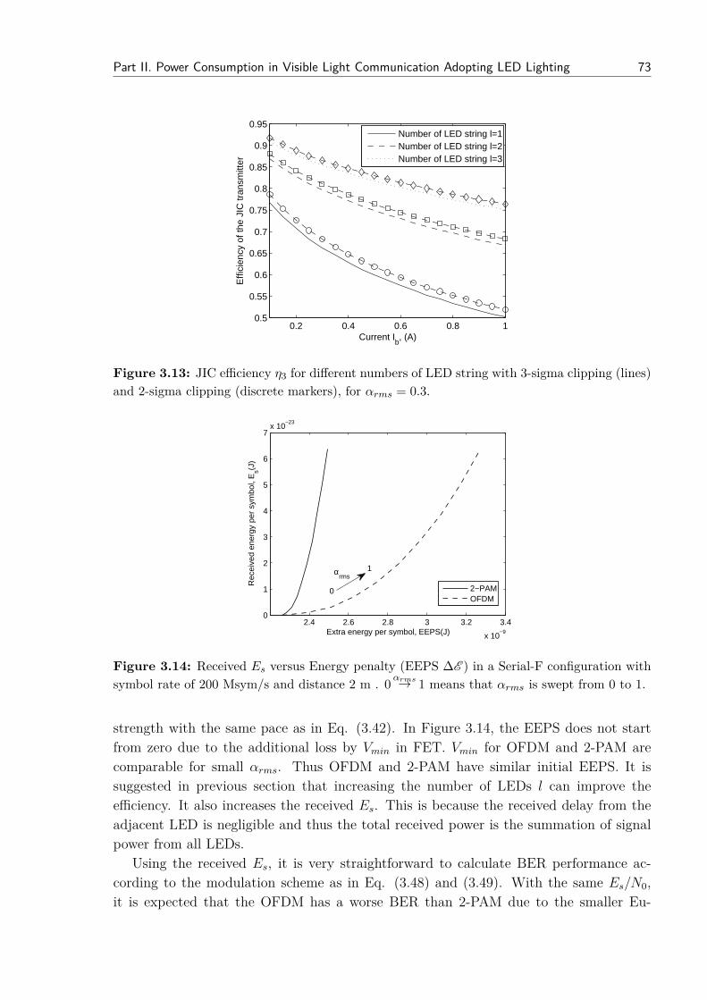
Part II. Power Consumption in Visible Light Communication Adopting LED Lighting 73
0.2 0.4 0.6 0.8 10.5
0.55
0.6
0.65
0.7
0.75
0.8
0.85
0.9
0.95
Current Ib, (A)
Effi
cien
cy o
f the
JIC
tran
smitt
er
Number of LED string l=1Number of LED string l=2Number of LED string l=3
Figure 3.13: JIC efficiency η3 for different numbers of LED string with 3-sigma clipping (lines)and 2-sigma clipping (discrete markers), for αrms = 0.3.
2.4 2.6 2.8 3 3.2 3.4
x 10−9
0
1
2
3
4
5
6
7x 10
−23
Extra energy per symbol, EEPS(J)
Rec
eive
d en
ergy
per
sym
bol,
Es(J
)
2−PAMOFDM
αrms
1
0
Figure 3.14: Received Es versus Energy penalty (EEPS ∆E ) in a Serial-F configuration withsymbol rate of 200 Msym/s and distance 2 m . 0 αrms→ 1 means that αrms is swept from 0 to 1.
strength with the same pace as in Eq. (3.42). In Figure 3.14, the EEPS does not startfrom zero due to the additional loss by Vmin in FET. Vmin for OFDM and 2-PAM arecomparable for small αrms. Thus OFDM and 2-PAM have similar initial EEPS. It issuggested in previous section that increasing the number of LEDs l can improve theefficiency. It also increases the received Es. This is because the received delay from theadjacent LED is negligible and thus the total received power is the summation of signalpower from all LEDs.
Using the received Es, it is very straightforward to calculate BER performance ac-cording to the modulation scheme as in Eq. (3.48) and (3.49). With the same Es/N0,it is expected that the OFDM has a worse BER than 2-PAM due to the smaller Eu-

74 Chapter 3. Modelling and Analysis for Transmitter Performance in Visible Light...
4.5 5 5.5 6 6.5 7 7.5
x 10−8
10−6
10−5
10−4
10−3
10−2
10−1
Extra energy per symbol, EEPS(J)
BE
R
2−PAM4−QAM OFDM16−QAM OFDM64−QAM OFDM256−QAM OFDMPreBER
αrms
0
0.3
Figure 3.15: BER versus Energy penalty (EEPS ∆E ) in a Serial-F configuration with a fixedsymbol rate of 10 Msym/s and distance 2 m. 0 αrms→ 0.3 means that αrms is swept from 0 to 0.3with step size of 0.03. We see a better BER for 2-PAM than 4-QAM OFDM with the sameαrms
.
clidean distance in a larger constellation size. Taking into account the extra energy foreach symbol ∆E , whose relation to Es is similar in Eq. (3.43), Figure 3.15 shows theBER performance versus the EEPS ∆E , where EEPS is proportional to f(αrms)Ts whileEs/N0 is proportional to α2
rmsTs. This makes the trade off between the sample rate andthe modulation depth of a different nature that we experience in typical radio RF systems.
In Fig 15, we plot the BER with a fixed symbol rate of 10 Msym/s for various con-stellation sizes and thus bit rates, i.e., 10, 10, 20, 30 and 40 Mbps for 2-PAM, 4-QAMOFDM, 16-QAM OFDM, 64-QAM OFDM and 256-QAM OFDM, respectively. The 4-QAM OFDM has a data rate of 10 Mbps other than 20 Mbps, due to the informationredundancy for a real-valued optical signal to satisfy the Hermitian symmetry property.We vary the modulation depth αrms, and calculate the EEPS from Eq. (3.23) and (3.34),and the BER from Eq. (3.48) and (3.49). In particular, to calculate PSF in Eq. (3.23), weused Eq. (3.29) and (3.33) for OFDM and 2-PAM, respectively. With the same data rateand αrms, 2-PAM is more attractive than 4-QAM OFDM due to its better performanceboth for ∆E and BER. Even more efficient PAM system is expected by increasing itsstep number.
Although the data rate of OFDM can benefit from a larger constellation size M ,it is not feasible due to the worse BER performance for large M . The reduced BERperformance is mainly caused by the decreased Euclidian distance in the constellation.Usually a Forward Error Correction (FEC) code needs a raw BER in the order of 10−3. Inparticular, there is a best Es/N0 and thus BER when αrms = 0.3 and αrms = 1 for OFDMand 2-PAM, respectively. However, in 2-PAM and small M -QAM OFDM, the BER canbe significantly below the PreBER bar for error correction and thus some energy for such

Part II. Power Consumption in Visible Light Communication Adopting LED Lighting 75
106
107
108
109
1010
1011
10−11
10−10
10−9
10−8
10−7
10−6
Data rate (bps)
Ext
ra e
nerg
y pe
r bi
t, E
EP
B(J
)
2−PAM4−QAM OFDM16−QAM OFDM64−QAM OFDM256−QAM OFDM
Figure 3.16: Energy penalty (EEPB ∆Eb) versus data rate in a Serial-F configuration with apre-BER ≤ 10−3 and distance 2 m. αpeak = 1 for OFDM (αrms = 0.3) and 2-PAM (αrms = 1).
(a) Data rate (bps)
Mod
ulat
ion
inde
x (α
rms)
106
108
1010
0
0.2
0.4
0.6
0.8
1
−105
−100
−95
−90
−85
−80
−75
−70
−65
(b) Data rate (bps)
Mod
ulat
ion
inde
x (α
rms)
106
108
1010
0
0.05
0.1
0.15
0.2
0.25
−90
−85
−80
−75
−70
−65
(c) Data rate (bps)
Mod
ulat
ion
inde
x (α
rms)
106
108
1010
0
0.05
0.1
0.15
0.2
0.25
−86
−84
−82
−80
−78
−76
−74
−72
−70
−68
−66
(d) Data rate (bps)
Mod
ulat
ion
inde
x (α
rms)
106
108
1010
0
0.05
0.1
0.15
0.2
0.25
−82
−80
−78
−76
−74
−72
−70
−68
Figure 3.17: Energy penalty (EEPB ∆Eb in dBJ) under different αrms and data rate in aSerial-F configuration, with a pre-BER ≤ 10−3 and distance 2 m. (a) 2-PAM; (b) 4-QAMOFDM; (c) 16-QAM OFDM; (d) 64-QAM OFDM.
BER is wasted from the energy prospective. To avoid the waste of the energy for BER 10−3 in these modulation methods, we should increase the symbol rate.
With the consideration of the number of information bits per symbol in differentmodulation methods as in Eq. (3.50), Figure 3.16 shows the EEPB ∆Eb versus the datarate with the best Es/N0, where all the modulation methods have a pre-BER lower than

76 Chapter 3. Modelling and Analysis for Transmitter Performance in Visible Light...
10−3 for a typical FEC code. Note that there is a EEPB difference between 2-PAMand OFDM in the order of 10−10 which is also indicated by the EEPS in Figure 3.14.It is expected that ∆Eb is inversely reduced with the data rate. Moreover even differentmodulation schemes have a similar ∆Eb under the same data rate that meets the pre-BERrequirement, which is however in contrast to the RF system where a high constellationsize usually has low energy efficiency. Without the waste of the energy for BER 10−3,we prefer 2-PAM since it can achieve a compelling extra energy per bit of 30 pJ/bit atthe data rate of 20 Gbps.
Since αrms also affects ∆Eb, Figure 3.17 shows the EEPB ∆Eb under different αrms anddata rate. We see that 2-PAM system also has a large dynamic range for the choice ofαrms and data rate. To meet the pre-BER requirement, αrms should be larger than 0.08,0.03, 0.06 and 0.14 for 2-PAM, 4-QAM OFDM, 16-QAM OFDM and 64-QAM OFDM,respectively. We also notice the dynamic range of 256-QAM OFDM is only aroundαrms = 0.3 and data rate of 40 Mbps, which is consistent with Figure 3.15.
3.7 Conclusion
This work studied the power penalty of a high-speed JIC transmitter by analyzing boththe extra power consumption and data rate capability. It showed that extra power isinevitably consumed for data transmission in a JIC transmitter. In the LED, the extrapower is dissipated due to the varying current and it is modulation-dependent. The extrapower loss for OFDM is more than that for 2-PAM signal. In a Bias-T configuration, theextra power is determined by the power efficiency of the additional amplifier while, in theSerial-F topology, the extra power is determined by the necessary voltage upswing. Inparticular, the Serial-F transmitter is compatible with most of modulation methods and itis easy for integration. Thus, we propose a Serial-F transmitter for high-speed OFDM and2-PAM systems using an efficient SMPS as the voltage source and a FET as the modulator.The extra power in FET is modulation-dependent since it operates in different regions fordifferent modulation methods. To improve the transmitter power efficiency for OFDMsignal, one can reduce the PAPR by clipping or increase the number of LEDs in the string.For instance, a Serial-F OFDM transmitter can achieve an efficiency of 87% by a stringwith 3 LEDs and 2-sigma clipping. Moreover, theoretical efficiency indicates that the 2-PAM can reuse parts of the illumination power for communication for a large modulationindex, e.g., η2 > 1 when αrms = 1. However the modulation method with a continuouswaveform such as OFDM cannot reuse the illumination power for communication, incontrast to the understanding of VLC as a green communication. We further show that2-PAM is more attractive than OFDM due to both the better BER, larger dynamic rangefor modulation depth, and the higher energy efficiency with a compelling minimum extraenergy per bit around 30 pJ/bit to achieve error-free communications.

CHAPTER 4
LED Power Consumption in Joint Illumination andCommunication System
This chapter is adapted from: X. Deng, Yan Wu, A. M. Khalid, Xi Long and J. P. M. G.Linnartz, ”LED Power Consumption in Joint Illumination and Communication System,” Opt.Express, vol. 25, no. 16, pp. 18 990–19 003, Aug 2017. c©OSA
Abstract – In Chapter 3, the extra power modelling for the JIC transmitter is based onthe assumption that the LED output optical power was proportional to its input current.However, the LED has a nonlinear relationship between the input current and outputoptical power due to the nonconstant quantum efficiency for different input current. Thischapter therefore further addresses the power penalty in an illumination LED caused byVisible Light Communication (VLC). This study models the extra power consumptionof the LED by taking into account the convex relation between the dissipated electricalpower versus the LED current on one hand and the concave relation between the outputluminous flux versus the current on the other hand. The ratio of the output luminous fluxto input electrical power, which is known the LED luminous efficacy, is analyzed consid-ering various recombination mechanisms and their dependency on current and tempera-ture. As examples, the rapid light fluctuations induced by Pulse Amplitude Modulation(PAM) and Orthogonal Frequency Division Multiplexing (OFDM) are analyzed for JointIllumination and Communication (JIC) systems. Due to the signal modulation, there isa decrease in the output light of LED. Nevertheless, the total power offered to LED islarger than without modulation and thus extra heating occurs. Moreover, particularlywhen burst transmission is used in communication networks, visible flicker may occur.
77

78 Chapter 4. LED Power Consumption in Joint Illumination and Communication System
4.1 Introduction
Light Emitting Diodes (LEDs) are now commonly used for both specialized and generalillumination applications. Because the LEDs have many advantages over traditional lightsources, such as high luminous efficiency, small size and long lifetime, they are believedto eventually replace conventional incandescent and fluorescent lamps for general lightingin future. At the same time, there has been a growing interest to apply Visible LightCommunication (VLC) to LED-based lighting systems. The primary purpose of a JointIllumination and Communication (JIC) system, e.g. [73, 133, 177], is to provide illumina-tion with data communication through VLC as a secondary function. Several challengesoccur in designing a JIC system such as to overcome data rate limitations and to minimizepower consumption. Many reported works demonstrated new functionalities or developedsignal processing techniques to increase data rate [4, 69, 156].
VLC is suggested to be a green technology since it modulates the current throughexisting illumination LEDs and reuses the illumination power for communication [10, 81,156]. Yet, there is a power penalty associated with operating LEDs at rapidly varyingpower levels. For instance, a Field Effect Transistor (FET) modulator in series with theLED consumes the extra power [33, 112]. Also in the LED itself, extra power loss occurs,due to the convexity of the diode equation[35, 112, 177]. Although the mentioned worksaddressed the power consumption issue, they mainly focused on the electrical performanceof LEDs or drivers.
As the first approximation, the output luminous flux is proportional to the averagecurrent (DC-bias) through LED with modulation [33, 134, 177]. However, because ofa modest degree of concavity between the luminous flux and the current, even DC-freemodulation also reduces the average light output [133]. The effect of a decreased luminousflux induced by Alternating Current (AC) modulation and pulse driving current, com-pared to a constant driving current was reported in [60, 63, 107]. Hence, in a JIC system,one must anticipate that data modulation decreases output luminous flux to some extent[151]. The reduction in light flux can be compensated by an increased current. Other-wise, the low-speed modulation effect in a burst data transmission, where the waiting (nomodulation) time is randomly distributed, can lead to perceivable flicker. This chapterquantifies the extra power consumption associated with the luminous flux compensationin the LED.
The output luminous flux of LED is determined not only by the current through theLED but also the temperature of the LED device, in particular the junction tempera-ture [97, 165]. These two factors also have effect on the spectrum of the LED and theeffectiveness of the phosphor, thereby affecting the colorimetric performance, includingthe Correlated Color Temperature (CCT), Color Rendering Index (CRI), and LuminousEfficacy of Radiation (LER) [44, 63, 115, 142]. In this chapter, we further refine themodel of LED light output into a system where multiple physical (e.g. electrical, thermaland photonic) mechanisms interact with each other, as shown in Figure 4.1. In the quasi-stationary mode, an increasing current will increase the LED output light, but it also

Part II. Power Consumption in Visible Light Communication Adopting LED Lighting 79
-
--+
Luminous flux
+
+Forward
voltage
+
Power
consumption
-
-
Temperature
+
Current
10 C / WTR
2.1 lm / Clm
3mV/ C
V
Efficacy
+ (positive effect); - (negative effect); (.) Equations
(16) (17)
(17)
/(10)(2)
(1)
(9)
Figure 4.1: Factors affecting the light output of the LED.
increases the forward voltage and thus it leads to increased power dissipation. The powerdissipation in the LED will increase the temperature, which in return decreases the lightoutput in terms of decreased efficacy. In the transient mode, the fast data modulationwith both up and down current also introduces increased power consumption but withreduced light output.
This chapter quantifies the LED power consumption, including the extra power lossinduced by data transmission. Figure 4.1 illustrates the interdependencies and refers tothe expressions that model the effects which are combined in this chapter to express theoverall efficacy decrease. In particular, we classify two nonlinear effects with respect tothe LED driving current I in this chapter. Firstly, for the luminous flux Φ−I nonlinearity,we refer to as ΦINL. Secondly, for the power consumption P − I nonlinearity which wasintroduced in[112], we refer to as PINL.
4.2 LED luminous flux versus current nonlinearity (ΦINL)
The perceived output of commercial lighting LEDs is usually described in photometricunits, such as the luminous flux in lumen (lm). To evaluate the link budget for commu-nication, the LED output also needs to be expressed in radiometric units such as radiantflux in Watts (W) [164]. Table 4.1 lists the photometric and radiometric units, where themost relevant units for our purpose are in bold.
In the following sections, we express LED luminous flux in terms of the driving currentand temperature.

80 Chapter 4. LED Power Consumption in Joint Illumination and Communication System
Table 4.1: Photometry and RadiometryPhotometric Units Radiometric Units
Luminous flux lm Radiant flux WLuminous intensity cd† = lm/sr? Radiant intensity W/srIlluminance lux = lm/m2 Irradiance W/m2
Luminance cd/m2 = lm/sr/m2 Radiance W/sr/m2
† cd refers to candelas; ? sr refers to steradian.
4.2.1 Luminous flux of LED versus current
The luminous efficacy of the LED source ηl, expressed in lm/W, is defined as the ratio ofthe luminous flux output ΦV in lm over the electrical power. Thus
ΦV = ηlPLED, (4.1)
where PLED = IV is the input electrical power at current I and voltage V . In fact ηlis mostly determined by two factors, namely the Luminous Efficacy of Radiation (LER),denoted as ηLER and Wall-Plug efficiency (WPE), denoted as ηWPE. So,
ηl = ηLERηWPE. (4.2)
4.2.1.1 Luminous Efficacy of Radiation (LER)
The LER, defined as the ratio of luminous flux to radiant flux [165], is given by
ηLER = Km
∫λ SLED(λ)V (λ)dλ∫λ SLED(λ)dλ , (4.3)
where Km is a constant with value of 683 and the integrals are taken over the wavelengthλ of the perceivable light. As we can see, ηLER is obtained by the relative Spectral PowerDensity (SPD) SLED (λ), weighted by the efficiency function V (λ) to take into accountthe relative sensitivity of eyes. For a given LED with a known and stable (e.g. currentindependent) spectrum, ηLER becomes a constant. In practice, perceivable chromaticityshift can occur [151], but be avoided by using an active feedback loop [44] and appropriatethermal design [115]. In this chapter, the relative SPD of LED is assumed to be fixed. Infact, Guoxing et al. [70] tested the effect of the driving current on the relative SPD andfound its effect to be negligible.

Part II. Power Consumption in Visible Light Communication Adopting LED Lighting 81
4.2.1.2 Wall-Plug Efficiency (WPE)The Wall-Plug efficiency (or radiant efficiency) of the source is defined as the ratio ofemitted optical power Pop, over the input electrical power [165], thus
ηWPE = PopPLED
= 〈Ep〉qV
Np
I/q= 〈Ep〉
qVηEQE, (4.4)
where 〈Ep〉 is the average energy of a photon, q is the electrical charge and Np is thenumber of photons per unit time. The External Quantum Efficiency (EQE) ηEQE isdefined as the ratio of the number of photons emitted into free space per second over thenumber of electrons injected into LED per second, so ηEQE = Np/(I/q). The EQE canbe seen as the combined effect of the Internal Quantum Efficiency (IQE) and the lightextraction efficiency, so it is expressed as
ηEQE = ηIQEηExt, (4.5)
where ηIQE is the ratio of photons generated by electron-hole recombination to the totalnumber of electrons injected into the LED, and ηExt is defined as the ratio of the photonsextracted out into the free space to the photon generated in the Quantum Well (QW). Itappeared reasonable to assume that ηExt remains constant for a varying injection currentlevel [199], so we only consider the efficiency droop in IQE. In GaInN/GaN LEDs, theefficiency droop is known as the gradual decrease of efficiency when the injection currentdensity surpasses a certain value [31].
To calculate the IQE, a generally accepted ABC model was used [30, 111, 150, 199].The carrier recombination can occur either as radiative recombination, during whichlight is generated or as the non-radiative recombination, without output light. The non-radiative recombination mechanisms include the defect-related Shockley-Read-Hall (SRH)recombination and Auger recombination[150]. For GaInN/GaN LEDs, the recombinationrate R is a polynomial function of the carrier concentration m, and it is written as
R = Am+Bm2 + Cm3, (4.6)
where A, B, and C represent the SRH recombination, radiative recombination, and Augerrecombination coefficient, respectively [150]. Since only the radiative recombination (ac-cording to the B-term) leads to light emission, we get
ηIQE = Bm2
R= B
A/m+B + Cm. (4.7)
Based on Eq. (4.7), an optimum IQE is reached when dηIQE(m)/dm = 0, thus at acarrier concentration of mp =
√A/C. The corresponding current for the optimum IQE

82 Chapter 4. LED Power Consumption in Joint Illumination and Communication System
0 50 100 1500.15
0.2
0.25
0.3
0.35
0.4
0.45
0.5
0.55
0.6
0.65
Current (mA)
Inte
rnal
qua
ntum
effi
cien
cy (
ηIQ
E )
Internal quantum efficiency versus current
η
IQE = − 5 ×10⁻¹¹×I5 +2.4 ×10⁻⁸×I4 −4.3 ×10⁻⁶×I3 + 0.00036×I2 − 0.016×I + 0.67
ABC modelPolynomial fitting with N=5
A= 107 s−1
B= 10−10 cm3s−1
C= 5*10−29 cm6s−1
Vactive
=3nm × 300µm × 300µm
Figure 4.2: Internal quantum efficiency versus current
can be calculated through the relation between the current and recombination rate, i.e.,Ip = qVactiveRp, where Vactive is the effective active region volume and Rp is calculatedfrom Eq. (4.6) using mp. Usually, the optimum IQE is achieved when Ip is below afew mA while beyond this point, the IQE decreases with rising current [25, 30, 31]. Inlighting systems where a power LED is used, the operation forward current is up to severalhundreds of mA. Thus, within the operation current range of the LED, we assume thatηIQE is a monotonically decreasing polynomial function of current I, viz.,
ηIQE =N∑n=0
dnIn. (4.8)
For a typical GaInN/GaN LED [30], the coefficients dn for a fifth order (N=5) fittingare compared in Figure 4.2 with the calculated IQE. The optimum IQE occurs around1mA and the fitting agrees well with the calculated IQE. The concavity of the LED outputlight versus current with ABC model is further calculated in Appendix A.
Inserting Eq. (4.2)-(4.5) and (4.8) into (4.1), we get
ΦV = 〈Ep〉q
ηLERηExtN∑n=0
dnIn+1, (4.9)
which is a nonlinear polynomial function of current I.
4.2.2 Thermal effect on LED luminous flux
The input power of the LED, PLED, is partially transmitted optically and partly dissipatedas heating, thereby decreasing the quantum efficiency and degrading the light output. Tomitigate temperature rises due to heating, a large heat sink can be used, but this wouldincrease cost, weight and size [147]. A typical thermal resistance from the junction to

Part II. Power Consumption in Visible Light Communication Adopting LED Lighting 83
the thermal pad is around RT = 10C/W, which causes a temperature increment of∆T = RTPLED (1− ηWPE)C. Figure 4.1 suggests that the thermal effect decreases theforward voltage of LED, typically in the order of ∆V = −0.003V/C and reduces theoutput luminous flux in the order of ∆lm = −2.1lm/C [107]. To calculate the outputlight by taking heating into account, an empirical exponential approximation has beenproposed in [12]
ΦV T ≈ ΦV exp [−kRTPLED (1− ηWPE)] , (4.10)
where k is a positive thermal coefficient. However, the time constant associated with theLED heating is relative slow and in the order of one millisecond [12]. In such case, it isreasonable to make a quasi-static approximation and assume that the LED temperatureis determined by the rms average current, which simplifies the analysis in the JIC system.Thus in this chapter, the thermal effect is only considered in the calculation of the extrapower loss when the LED is driven at different illumination levels.
4.3 Extra power loss due to ΦINL and modulation
Equation (9) and (10) show that the output luminous flux increases non-linearly withthe current through the LED. Hence modulation across this concave function leads toa reduced output, but that can be compensated by increasing the input power. In thissection we will evaluate the associated extra power loss and illustrate it for a typicalcommercial LED.
4.3.1 Luminous flux of a commercial white LED
For a Luxeon Rebel power LED [117], the output luminous flux is shown in Figure 4.3versus the input current. Since higher order terms are negligible, we approximate Eq.(4.9) by a concave quadratic function
ΦV ≈ aI2 + bI + c, (4.11)
where I is in mA. For the Luxeon Rebel, a = -0.000102, b = 0.309 and c = 3.65, with athermal pad temperature of 25C maintained.
Figure 4.3 shows a pronounced difference between a thermal pad that maintains atemperature of 25C versus without a heat sink. Equation (10) with k = 0.01 is alsoshown in Figure 4.3. Practical heat sinks will perform in the gray area of Figure 4.3.
4.3.2 Extra power for luminous flux compensation
In this section we compensate for the flux loss that we described in the introduction.When a modulation signal s(t) is superimposed upon an average current I, the time-varying current through the LED is expressed as I(t) = [1 + s(t)]I. Within the 3-dB

84 Chapter 4. LED Power Consumption in Joint Illumination and Communication System
Forward current (mA)
Lum
inou
s flu
x (
lm)
Luminous flux versus forward current
0 200 400 600 800 10000
50
100
150
200
250
Measured with 25 °C maintainedQuadratic fittingMeasured with heating effect
ΦV = − 0.000102×I2 + 0.309×I + 3.65
Figure 4.3: Luminous flux output of a typical commercial white LED
bandwidth of the LED, we can assume the luminous flux instantaneously follows themodulated current I(t). In such case and for a maintained thermal pad temperatureof 25C, the relation between the mean value of luminous flux level E [ΦV ] and averageforward current I follows
E [ΦV ] =∫IP (I)
a[1 + s(t)]2I2 + b [1 + s(t)] I + c
dI
= ΦV (I) + (2aI2 + bI)E [s(t)] + aI2E[s2(t)
] , (4.12)
where P (I) is the distribution of the modulated current and ΦV (I) is calculated fromEq. (4.11) using I. Since we assumed elsewhere the temperature does not depend onthe fluctuation of modulated current, here the temperature is not depend on the currentRoot-Mean-Square (RMS) value. We have E [s2(t)] = α2
rms, where αrms is the aver-age modulation index which equals the RMS value of s(t), and for DC-balanced signalE [s(t)] = 0. When a binary modulation such as two-level Pulse Amplitude Modula-tion (2-PAM) is adapted with two current levels [1− αm, 1 + αm]I and equal probability,E [s2(t)] becomes equal to α2
m.Due to the nonlinear coefficient a in Eq. (4.12), any DC-balanced modulation signal
such as OFDM signal will lead to decreased luminous flux, which can be only compensatedby increasing the (DC) input current. Otherwise, the low-speed modulation effect in thedata frame can lead to perceivable flicker. To avoid potential flicker perception andachieve an expected illumination level, the current should be increased from I to somevalue ID, as illustrated in Figure 4.4. The current increment ∆I = ID − I reflects theincreased power consumption. We can find the desired average current ID that deliversthe expected illumination level, by drawing a horizontal line through the static operationlevel, i.e., ΦV (I), and find the crossing with the (timesharing) straight line between thetwo modulation levels ΦV [(1− αrms)I] and ΦV [(1 + αrms)I]. Mathematically, we find IDby solving a re-written version of Eq. (4.12) with ID and Eq. (4.11) with the current I

Part II. Power Consumption in Visible Light Communication Adopting LED Lighting 85
I (1 )rms I(1 )rms II
V
Expected
Illumination
level
Illumination
level without
compensation
IDI
Figure 4.4: LED luminous flux nonlinearity
0.5
0.5
0.5
0.5
1
1
1
1
2
2
2
2
4
4
4
4
8
8
8
16
16
16
30
30
60
120
Communication (αrms
)
Illum
inat
ion
( Φ
V, (
lm))
Current increment for flux compensation (mA)
0.1 0.2 0.3 0.4 0.5 0.6 0.7 0.8 0.9 1
20
40
60
80
100
120
Empirical line
ΦV × α
rms = 15
Figure 4.5: Current increment under different illumination level and modulation index
for unmodulated signals, as
E [ΦV ] = aI2 + bI + c
= aI2D + bID + c+ (2aI2
D + bID)E [s(t)] + aI2DE
[s2(t)
]. (4.13)
The current increment ∆I for the flux compensation is shown in Figure 4.5 for variousmodulation indexes and flux levels. As we can see, a substantial current increment isneeded for communication to maintain the same illumination level. In particular, theextra current could be more than 120mA when the modulation index is around 1 andthe expected flux is around 120 lm. Many reported works mainly consider that thesame average current would result into the same illumination level, which however is notaccurate, since we need to compensate for luminous efficacy nonlinearity. As a rule ofthumb, to avoid substantial extra power loss (∆I < 2mA), the product of the illuminationlevel and modulation index should be less than 15.

86 Chapter 4. LED Power Consumption in Joint Illumination and Communication System
Then, the extra power used for flux compensation in LED is calculated by
∆PLED flux = PLED(ID)− PLED(I), (4.14)
where PLED(.) is a monotonically increasing function with the input current, which willbe discussed next section.
4.4 Extra power loss due to PINL and modulation
The current through a LED follows the diode equation
I(t) = Is
[exp
(qV (t)nkT
)− 1
], (4.15)
where Is is the saturation current of the LED, q is the charge of an electron, V (t) is thevoltage across the junction, n is the ideality factor (n = 1 to 2), k is Boltzmann constantand T is the temperature in Kelvin. At room temperature kT/q = 26mV. The current Ishighly depends on the LED type, where a typical example is Is = 4.1×10⁻²⁴ with n = 1.4[141]. Above a few milliamps, the resistance RL in the LED needs to be considered, andit is typically a few ohms. The total voltage across LED becomes
V (t) = nkT
qln[I(t)Is
+ 1]
+RLI(t). (4.16)
In particular, for a constant current level, thus if I(t) = ID, the power into the junctionof LED plus its series resistance becomes
PLED(ID) = nkT
qID ln
[IDIs
+ 1]
+RLI2D. (4.17)
Clearly, this is a convex function of ID. Based on Jensen’s inequality, the convexrelationship, between the dissipated electrical power and current, leads to the extra powerloss when the LED is modulated for data transmission, as shown in Figure 4.6, where theextra power for ΦINL is also illustrated.
In particular, ∆I covers the luminous flux compensation, corresponding to Eq. (4.14).In this section, the extra power loss due to PINL is quantified, comparing binary modu-lation (2-PAM) and continuous modulation (OFDM).
4.4.1 Binary modulation
Based on Eq. (3.10) and (3.11), when binary modulation is adapted with two currentlevels [1− αm, 1 + αm]ID and with equal probability, the extra power in the LED is
∆PLED PAM = nkT
qID ·B +RLI
2Dα
2m. (4.18)

Part II. Power Consumption in Visible Light Communication Adopting LED Lighting 87
I(1 )rms DI(1 )rms DI
( )LEDP I
I
( )LED DP I
PLED
DII
Extra power for
( )LED DP I
ΦINLExtra power for
PINL
Figure 4.6: Two mechanisms of the extra power loss in the LED
4.4.2 Continuous modulation
Similarly, based on Eq. (3.7) for an OFDM transmitter, the extra power loss in the LEDbecomes
∆PLED OFDM = a2rms
(nkT
qIb +RLI
2b
), (4.19)
which also expresses the signal power.
4.5 Numerical Results
This section presents numerical results for the extra power loss in the LED. We firstcompare the losses caused by two mechanisms, namely the ΦINL and PINL in the LED.We compare the total extra power loss for different illumination levels and modulationindexes, and we further validate our rule of thumb to avoid substantial extra power loss.At last, the efficacy is discussed.
4.5.1 Extra power loss of the LED
Due to the ΦINL and data modulation, extra power is lost for luminous flux compensation.It is quantified from Eq. (4.11)-(4.14) and (4.17), as shown in Figure 4.7. The numericalresults for the loss due to the PINL are also shown in Figure 4.7, calculated by Eq.(4.18) and (4.19) for 2-PAM and OFDM, respectively. Figure 4.7 shows that the extrapower loss owing to the ΦINL dominates the extra power consumption. As expected, ahigher modulation index results in more extra power loss. Moreover, the extra loss due toPINL depends on the modulation waveform, in particular the OFDM needs more extrapower than 2-PAM. The waveform-dependent power loss in LED along with that in themodulator results into different overall energy efficiencies for different modulations, aspresented in [33].

88 Chapter 4. LED Power Consumption in Joint Illumination and Communication System
0 0.1 0.2 0.3 0.4 0.5 0.6 0.7 0.8 0.9 110
−1
100
101
102
103
Modulation Index (αrms
)
Ext
ra p
ower
loss
(m
W)
Extra power loss in LED for 100 lm
Extra power for ΦINLExtra power for PINL: OFDMExtra power for PINL: 2−PAM
Figure 4.7: Extra power loss of two mechanisms in LED
0 0.1 0.2 0.3 0.4 0.5 0.6 0.7 0.8 0.9 10
20
40
60
80
100
120
Communication (αrms
)
Illum
inat
ion
( Φ
V, (
lm))
Extra power loss of the LED (mW)
2
2
2
22
5
5
5
5
10
10
10
10
20
20
20
20
40
40
40
80
80
80
160
160
320
640
Empirical line
ΦV × α
rms = 15
Figure 4.8: Extra power loss in LED with OFDM
For OFDM signal, the extra power loss for different illumination levels and modulationindexes is shown in Figure 4.8. Results for 2-PAM are slightly better than OFDM. Figure4.8 shows that the power loss varies from 2 to 640 mW. A system designer should makea tradeoff between the illumination level and the amount of energy for communication(αrms), according to the extra power budget for data transmission through VLC. In otherwords, we believe that rather than expressing the Bit Error Rate (BER) for VLC versusthe Signal to Noise Ratio (SNR), we preferably benchmark solution for their ”extra”power loss, discounting the illumination power that is already available [112].
Higher illumination level tends to consume more extra energy if αrms keep constant.This is due to the fact that the high illumination level needs high current which leads tothe decrease of the efficacy.
In particular, the extra power directly dissipated as heating and thus the LED junctiontemperature also fluctuates in a burst data transmission. Our proposed design rule withextra ∆I < 2mA would enable the extra power loss to be less than 10 mW for an illu-mination system that consumes several Watts. This rule is effective to avoid substantial

Part II. Power Consumption in Visible Light Communication Adopting LED Lighting 89
506065
70
70
75
75
80
80
80
85
85
85
85
90
90
90
90
95
95
95100
100
100
105105
105110
110110120 120120
140 140 140
200 200 200
Communication (αrms
)
Illum
inat
ion
( Φ
V, (
lm))
Efficacy of the LED (lm/W)
0.1 0.2 0.3 0.4 0.5 0.6 0.7 0.8 0.9 1
20
40
60
80
100
120
Figure 4.9: Efficacy with different illumination and modulation index
thermal fluctuation that has side effect on the LED lifetime.
4.5.2 LED efficacy for joint illumination and communication
Since the efficacy is a key performance indicator for the LED systems, we plot in Figure 4.9the efficacy when the data transmission is applied. For low (dimmed) illumination levelsat 10 to 120 lumen, the efficacy decreases substantially even without current modulation.This is mainly due to the decrease of the internal quantum efficiency and the heatingeffect. Moreover, it is interesting to notice that for very low illumination levels, datamodulation would have no substantial effect on the efficacy.
4.6 Conclusion
This work showed that extra power was inevitably consumed in an illumination LEDwhen it was used for data transmission. The extra power loss appeared to come from twodifferent mechanisms, namely the output luminous flux nonlinearity (ΦINL) and powerconsumption nonlinearity (PINL) in the LED. We studied that LED luminous flux wasnonlinear with respect to the current due to the decrease of external quantum efficiencyand heating effect. The heating effect can be modelled in a quasi-stationary way forhigh-speed data transmission due to the slow thermal time constant. We found the extrapower due to PINL was modulation-dependent, for instance, OFDM consumes more extrapower than 2-PAM. The fluctuation of light intensity due to ΦINL is relatively small (afew percent), but it can lead to visible flicker in burst mode transmission and lead toperceivable light output differences when only a fraction of the lamps in a ceiling areused for VLC. The extra power for light compensation and PINL are dissipated as extraheating (up to several degrees), which have an impact on LED life time. Thus, LEDthermal design should be optimized by taking into account the modulation in emergingJIC systems.

90 Chapter 4. LED Power Consumption in Joint Illumination and Communication System

Part III: Interference Considerations inVisible Light Communication


CHAPTER 5
Performance Analysis for Joint Illumination and VisibleLight Communication using Buck Driver
This chapter is adapted from: X. Deng, Y. Wu, K. Arulandu, G. Zhou and J. P. M. G. Linnartz,”Performance comparison for illumination and visible light communication system using buckconverters,” 2014 IEEE Globecom, Austin, TX, 2014, pp. 547-552. c©IEEEAnd from: X. Deng, J. P. M. G. Linnartz, K. Arulandu, G. Zhou and Y. Wu, ”Effect of buckdriver ripple on BER performance in visible light communication using LED,” 2015 IEEE In-ternational Conference on Communication (ICC), London, 2015, pp. 1368-1373. c©IEEEAnd from: X. Deng, K. Arulandu, Y. Wu, G. Zhou and J. P. M. G. Linnartz, ”System modelingand analysis for LED-based Visible Light Communication using Buck Driver,” IEEE Transac-tions on Communications, vol. PP, no. 99, pp. 1–1, 2018. c©IEEE
Abstract – The Visible Light Communication (VLC) can provide data transmissionvia the illumination Light Emitting Diodes (LED). This chapter introduces a new modelto analyze the Bit Error Rate (BER) of Binary Phase Modulation (BPM) in VLC foran arbitrary modulation depth and data duty cycle while taking into account both theGaussian and signal-dependent shot noise. The impact of the driver design on the BERand its impact on ripple, have not been considered in detail before. We compare two dif-ferent LED driver schemes, namely directly adapting the driver control loop and binaryshunting. We address data rate, BER and power efficiency, for which we propose to usethe Extra Energy Per Symbol (EEPS) above unmodulated light. We further introducean analysis of the effect that (truncated) ripple interference has in the (matched or other)filter of the receiver. Ripple causes a harmful interference in VLC and thus a BER ex-pression is derived to include its effect. Two approximations are proposed to model theripple interference and their accuracies are compared by simulations. A low-pass filteringis proposed to alleviate the impact of ripple interference in VLC system.
93

94 Chapter 5. Performance Analysis for Joint Illumination and Visible Light Communication...
5.1 Introduction
Visible Light Communication (VLC), sometimes called Joint Illumination and Communi-cation (JIC), refers to a communication system that uses a lighting system to communicatedata [10]. VLC is appealing for a wide range of applications such as indoor broadband ac-cess [45], indoor positioning [191], distributed lighting remote control [168], entertainmentinteraction [110], intelligent sensing and ambient atmosphere rending [113, 114]. Yet, thecommunication performance can be affected by illumination constraints [50, 56, 189] andmodulation typically leads to a power penalty [35, 38, 112, 177]. This chapter studies thecommunication performance in indoor applications where increasing the data rate is notthe highest priority, such as in intelligent sensing or in indoor positioning.
Several modulation schemes have been proposed for JIC systems. For high modu-lation speeds, significantly above the flat pass-through band of the LEDs, multi-carrierapproaches such as Orthogonal Frequency Division Multiplexing (OFDM) have been in-vestigated extensively, e.g. in [45, 133]. However, at lower rates, sequential transmissionof symbols at baseband is more popular: On-Off Keying (OOK), Variable Pulse PositionModulation (VPPM) and Color-Shift Keying (CSK) are recommended in the IEEE stan-dard 802.15.7 [2]. To accommodate dimming, a Pulse-Width Modulation (PWM) wasproposed in [113, 114] with a variable duty cycle.
In this chapter, we focus on modulation methods with sequential symbols at baseband.In particular, we consider a class of Binary Phase Modulation (BPM), i.e., data symbolsthat consist of two parts with different amplitudes. By taking appropriate parameterchoices, our BPM model covers 2-PPM, OOK and Manchester-encoded OOK. VPPM[23, 140] is another widely studied form of BPM. Its Bit Error Rate (BER) performancewas analyzed in [144] and in [194] for full depth modulation. Although this gives the bestcommunication performance, less deep modulation is often preferred to mitigate visibleflicker [149, 159, 183], as the modulation index (depth) corresponds to ”percent flicker”[15].
One of the contributions of this chapter is that we will show that low modulationdepths are relatively more power efficient, e.g., the power loss per symbol increases fasterwith increasing modulation depth than that the SNR can benefit from the increased sig-nal strength. To this end, we express not only the energy per bit, as seen from an SNRcommunication perspective, but also the extra energy required to generate the bits.The signal power used in Signal-to-Noise Ratios (SNR) in most previous papers refers tothe total signal power, which predominantly is a function of the illumination intensity.Yet, VLC modulates the light already used for illumination but does not introduce morelight [10]. So, the additional power lost in electronic components, on top of the illumina-tion power is a more appropriate measure. Such power penalty associated with rapidlymodulating the LED current was studied for a Field Effect Transistor (FET) modulatorin series with the LED [33]. The losses in the LED itself was addressed in [38, 112].Switched Mode Power Supplies (SMPS), such as a Boost-converter LED driver [23] and aBuck-converter LED driver [127], have been proposed to drive the LED and to modulate

Part III. Interference Considerations in Visible Light Communication 95
r(t)
LED Driver
Binary
dataBPM
Maping
b x(t)X(t)
LED
h(t)PD
Y(t)
Transmitter
Free sp
ace
SNR0
sT
dt
Dec
isio
n
b
Receiver
0( )t
1( )t
r0
r1
Illumination Control
n(t)
nr(t)
Hf (f)
Ch
an
nel
0
sT
dt
Figure 5.1: Communication chain for VLC.
by means of switching on and off the current. Modulation by binary shunting [127, 129]can be attractive but may lead to a severe efficiency penalty [33, 37]. In this chapter,we further extend this analysis by including power losses in drivers. We verify our newanalytical models via a Spice simulation for the circuit and a Monte-Carlo simulation forits BER.
Reliable communication requires a clean DC-bias current through the LEDs with onlylimited flicker at frequencies where the human eye would be insensitive. Nonetheless,we show that a well designed receive filter can handle substantial ripple amplitudes. Wequantify to what extent required reduction of ripple affects the efficiency of the SMPS.
The rest of the chapter is organized as follows. Section 5.2 describes the JIC system.The theoretical BER performance of BPM is analyzed in Section 5.3, considering arbitrarymodulation depth and duty cycle. We also model signal-dependent shot noise, as it variesover the two phases of the symbol duration. Section 5.4 presents two LED drivers thatcan support BPM. We propose a control-loop adapting scheme that directly modulatesvia the SMPS and we show that this is highly efficient. Section 5.5 analyzes of the effectof ripple interference on the BER. Numerical and simulation results are depicted anddiscussed in Section 5.6. Here a low-pass filtering is proposed in our system to furthereliminate the ripple interference. Conclusions are drawn in Section 5.7.
5.2 System Description
As shown in Figure 5.1, a typical VLC system consists of a transmitter, a receiver andan optical channel.
The transmitter is composed of a data modulator, an illumination controller, a driverand LEDs. In a SMPS driver, a transistor switches on the current through the inductorand LEDs until a maximum current is reached. Then the current supplied by a DCsource is interrupted, yet a diode allows the current flowing through the inductor andLEDs, resulting in a reduced intensity of the current. Below a certain threshold, the DCsupply is connected again to increase the current. Hence, the current passing throughthe LEDs exhibits a high-frequency fluctuation (typically a few hundreds of kHz [127]),determined by the difference of the two thresholds, thus with an hysteresis that determinesthe ripple amplitude. For BPM signals, we consider two different driver methods [182].
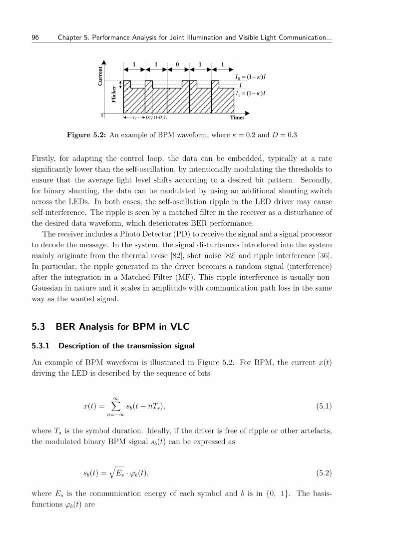
96 Chapter 5. Performance Analysis for Joint Illumination and Visible Light Communication...
Times
Cu
rren
t 1 1 0 1 1
Flick
erDTs
0 (1 )I I
(1-D)Ts
1 (1 )I I
Ts
I
0
Figure 5.2: An example of BPM waveform, where κ = 0.2 and D = 0.3
Firstly, for adapting the control loop, the data can be embedded, typically at a ratesignificantly lower than the self-oscillation, by intentionally modulating the thresholds toensure that the average light level shifts according to a desired bit pattern. Secondly,for binary shunting, the data can be modulated by using an additional shunting switchacross the LEDs. In both cases, the self-oscillation ripple in the LED driver may causeself-interference. The ripple is seen by a matched filter in the receiver as a disturbance ofthe desired data waveform, which deteriorates BER performance.
The receiver includes a Photo Detector (PD) to receive the signal and a signal processorto decode the message. In the system, the signal disturbances introduced into the systemmainly originate from the thermal noise [82], shot noise [82] and ripple interference [36].In particular, the ripple generated in the driver becomes a random signal (interference)after the integration in a Matched Filter (MF). This ripple interference is usually non-Gaussian in nature and it scales in amplitude with communication path loss in the sameway as the wanted signal.
5.3 BER Analysis for BPM in VLC
5.3.1 Description of the transmission signal
An example of BPM waveform is illustrated in Figure 5.2. For BPM, the current x(t)driving the LED is described by the sequence of bits
x(t) =∞∑
n=−∞sb(t− nTs), (5.1)
where Ts is the symbol duration. Ideally, if the driver is free of ripple or other artefacts,the modulated binary BPM signal sb(t) can be expressed as
sb(t) =√Es · ϕb(t), (5.2)
where Es is the communication energy of each symbol and b is in 0, 1. The basis-functions ϕb(t) are

Part III. Interference Considerations in Visible Light Communication 97
ϕ0(t) =
(1 + κ)/ϕ∆, 0 ≤ t < DTs(1− κ)/ϕ∆, DTs ≤ t ≤ Ts
, (5.3)
ϕ1(t) =
(1− κ)/ϕ∆, 0 ≤ t < (1−D)Ts(1 + κ)/ϕ∆, (1−D)Ts ≤ t ≤ Ts
. (5.4)
where ϕ∆ = [D(1 + κ)2 + (1−D)(1− κ)2]Ts1/2 normalizes the signal power and suchthat
∫ Ts0 ϕ2
b(t)dt = 1. The modulation index κ (0 < κ < 1) is defined as the ratio of thecurrent difference over the sum of the currents, so κ = (I0 − I1)/(I0 + I1), where I0 andI1 are the currents in the higher and lower state, respectively. As special cases of BPM,we have D = 1 and κ = 1 for OOK, and D = 0.5 and κ = 1 for 2-PPM and full-depthManchester-encoded OOK. In particular, practical systems prefer a smaller modulationindex to mitigate potential visible artefacts.
5.3.2 VLC channel model
Intensity Modulation and Direct Detection (IM/DD) over a wireless optical channel canbe modeled as a baseband linear system with an optical input signal X(t), an outputcurrent r(t), a channel equivalent impulse response h(t) and additive Gaussian noise n(t)[82, 83]. The received signal is expressed as
r(t) = εX(t)⊗ h(t) + n(t), (5.5)
where ε is the responsivity (A/W) of the PD. For data rates below one megabit persecond, the multipath propagation dispersion may typically be neglected. Moreover, thelow-pass responses in LED and in the phosphor are not addressed explicitly in the scopeof this chapter. Assuming Lambertian radiation for LEDs [51, 82], we have
h(t) = µρδ(t) = µA(m+ 1)cosm(φ) cos θ2πd2 δ(t), (5.6)
where µ is the responsivity (W/A) of LED, ρ denotes the optical channel DC gain and δ(t)is the impulse function. To calculate ρ, A, φ, θ, d are the surface area of the PD, off-axisangle relating to the transmission direction of the main band, off-axis angle relating todirection of PD, and the distance between the lamp and detector, respectively. The orderm is related to the semi-angle via m = − ln 2
/ln(cos Φ1/2), where Φ1/2 is the semi-angle
at half power of the LEDs. Thus we receive
r(t) = H√Esϕb(t) + n(t), (5.7)

98 Chapter 5. Performance Analysis for Joint Illumination and Visible Light Communication...
where H = εµρ. The signal-dependent noise n(t) in the optical channel has zero meanand its variance is the sum of shot noise σ2
shot and thermal noise σ2thermal [161]. The
variance is calculated by
σ2n(t) = σ2
shot + σ2thermal = 2qεPn(t)Bn + 4kT
RF
Bn, (5.8)
where q, Pn(t), Bn, k, T , RF are the electrical charge of an electron, the received powerat the PD, effective bandwidth, Boltzmann’s constant, absolute temperature and feed-back resister of the Trans-Impedance Amplifier (TIA) in the receiver, respectively. Thevariance of the shot noise is proportional to all light power Pn(t) seen by the PD, notonly ambient light, but also the modulated VLC signal itself. If the VLC system deliversall illumination, thus in the absence of other ambient light, the light intensity that leadsto shot noise is
Pn(t) = µρ√Esϕb(t). (5.9)
Hence, as we will address later, the variance of the shot noise varies within one symbol.
5.3.3 Received BER performance
A Matched Filter (MF) receiver multiplies the signal with a synchronized template ϕb(t)of each possible symbol in the alphabet b ∈ 0, 1 , described by ∧
ϕb(t) = 1µρϕb(t)⊗h(t) =
ϕb(t), and then integrates over the whole symbol duration Ts. For b = 0, the two decisionvariables are recovered by the MF as
r0(b = 0) = ερµ
√Es + n0
r1(b = 0) = ερµ√Es.α0 + n1
, (5.10)
where the correlation coefficient α0 is defined as α0 =∫ Ts0∧ϕ0(t) ∧ϕ1(t)dt, which depends on
D and κ based on Eq. (5.3) and (5.4).The two Gaussian noise terms n0 and n1 are zero mean and have variance of σ2
n0 andσ2n1. The variance of such noise terms is
σ2n0 = E
[∫ Ts
0n(t) ∧ϕ0(t)dt
]2− E2
[∫ Ts
0n(t) ∧ϕ0(t)dt
]
=∫ DTs
0
∫ DTs
0E[n(t)n(s)] ∧ϕ0(t) ∧ϕ0(s)dtds+
∫ Ts
DTs
∫ Ts
DTsE[n(t)n(s)] ∧ϕ0(t) ∧ϕ0(s)dtds
,
(5.11)

Part III. Interference Considerations in Visible Light Communication 99
where E[n(t)n(s)] = σ2n(t)δ(t−s)/Bn. After splitting the integral into periods of constant
noise variance using Eq. (5.8) and defining L = 2qερµ√Es, we get
σ2n0 = L
[∫ DTs
0ϕ3
0(t)dt+∫ Ts
DTsϕ3
0(t)dt]
+ 4kTRF
= L(1 + κ)3DTsϕ3
∆+ L(1− κ)3(1−D)Ts
ϕ3∆
+ 4kTRF
, (5.12)
which is signal-dependent due to the shot noise. Similarly, in the second branch, we have
σ2n1 = L(1 + κ)α1
ϕ∆+ L(1− κ)(1− α1)
ϕ∆+ 4kT
RF
, (5.13)
where coefficient α1 is defined as α1 =∫DTs
0 ϕ21(t)dt.
The receiver decides on a zero or a one by comparing the signals in the two branches,based on the decision parameter z = r0 − r1 which has expectation and variance
E [z|b = 0] = ερµ√Es.(1− α0),
Var [z|b = 0] = σ2n0 + σ2
n1 − 2ρκ,(5.14)
where we define the common noise power
ρκ = L(1 + κ)ϕ∆
α2 + L(1− κ)ϕ∆
(α0 − α2) + 4kTRF
α0, (5.15)
and the coefficient α2 is α2 =∫DTs
0∧ϕ0(t) ∧ϕ1(t)dt.
If z = r0 − r1 > 0, the receiver decides b = 0, otherwise b = 1. For equally likely bitswith P b = 0 = P b = 1 = 1/2, the error probability of BPM can be expressed as
Pe = 12erfc
ερµ√Es.(1− α0)√
2(σ2n0 + σ2
n1 − 2ρκ)
. (5.16)
Two limiting cases can be verified: (1) No modulation: If κ = 0 (regardless of D)or if D = 1 (regardless of κ), the correlation coefficient α0 = 1. Thus, Pe = 0.5, so nodata transmission occurs. Moreover, the LED driver is then not affected by the data, itmaintains high power efficiency, so we use this as a reference. (2) Binary shunting (κ = 1):The BER expression confirms that, the best BER performance occurs for α0 = 0 but, aswe will see later, the power efficiency is limited.
5.4 LED Driver Model for BPM
The BPM waveform depicted in Figure 5.2 can be generated by a widely used buckconverter, as shown in Figure 5.3. With full modulation depth (κ = 1), can easily be

100 Chapter 5. Performance Analysis for Joint Illumination and Visible Light Communication...
PWM
D1
f1T1
LED
C
L
Switch1
Ron1RL
RC
Von
Diode
RLED
VonCd
Ron2
Switch2
fsTs
Vdc
Il Ic V0
VLC
CTRL
1 D28V
Rsense
VLC
(b) Binary shunting (a) Control-loop adapting
I0
Figure 5.3: Proposed LED driver for BPM using Buck converter
obtained by a binary shunt Switch2, parallel to the LED. For arbitrary modulation depth(0 ≤ κ < 1) one preferably adapts the control loop.
The buck converter is popular in power systems as it is efficient, simple, stable andcost effective. It actually is a step-down DC to DC converter with a SMPS that usestwo switches (in fact, a MOSFET and a diode), an inductor and a capacitor [47]. It canoperate either in Continuous Conduction Mode (CCM) or in Discontinuous ConductionMode (DCM). In this chapter, we consider CCM, such that the current flowing throughthe inductor never fully falls to zero within the switching cycle of the converter and theaverage output voltage V0 can be expressed as V0 = D1Vdc, where D1 is the PWM dutycycle of MOSFET Switch1 and Vdc is the supply voltage of the driver.
5.4.1 Energy efficiency of control-loop adapting
To create an arbitrary modulation depth, we propose to adapt the threshold voltage ofthe control-loop inside the buck self-oscillating feedback circuit, as depicted in Figure 5.3(a). The efficiency of the LED driver in the electrical domain is defined as
η = E [Pout(t)]E [Pout(t)] + E [Pbuck(t)]
, (5.17)
where E[.] are the expectation of the output power and power dissipated in Buck driver. Ingood approximation, E[Pout(t)] is dominated by the switching loss Psw plus the conductionlosses Pcon. For a Buck converter that operates at frequency f1 with duty cycle D1 inCCM,
Psw = VdcI0f1 (tcr + tvr + tcf + tvf )/2, (5.18)
and
Pcon = I20RL + I2
0Ron1D1 + I0Von (1−D1) + (Il − I0)2Rc, (5.19)
where RL, RC are the Equivalent Series Resistance (ESR) of the inductor L and of thecapacitor, respectively. Il, I0 are the current in the inductor and the current drivingthe LEDs, respectively. We calculate Psw using typical values for the current rising time

Part III. Interference Considerations in Visible Light Communication 101
tcr, the voltage falling time tvf , the current falling time tcf , the voltage rising time tvr.Conduction losses dominate (Pcon Psw) and occur mainly in the transistor and theinductor L. Since Switch1 only conducts I0 during duty cycle D1, the losses in Ron1
are I20Ron1D1, where I0 is fairly constant for the conversion mode that we consider here.
Substantial losses occur in DC resistance RL of the inductor, namely I20RL. Also the on-
voltage Von across the diode contributes significantly with ILVon (1−D1). The currentthrough the capacitor is very small and thus the power loss in capacitor is negligible.
Simulations confirm that, for an average (DC) current I0, the power loss of the driverPbuck0 can be approximated by [112]
Pbuck0 ≈ c1I0 + c2I20 , (5.20)
where the loss coefficients are calculated by c1 = Von(1−D1) and c2 = RL + Ron1D1. Inour example, using a (Shottkey) Diode, c1 is 0.2 to 0.7 V and c2 is typically 1.2 Ohm.
Since the power loss is a convex function of the output current, some extra power lossis then dissipated in the Buck converter due to modulation [37]. For a BPM signal inEq. (5.1), the modulated signal is proportional to x(t) with middle (but not necessarilythe average) current I = (I0 + I1)/2. Then, the extra power in the Buck converter is theexpectation of Pbuck(t) minus the loss Pbuck0 without modulation. Hence,
∆Pbuck = E [Pbuck(t)]− Pbuck0 = c1I [2Dκ− κ] + c2I2[κ2 − 2κ+ 4Dκ
], (5.21)
where, similar to Eq. (5.20), Pbuck(t) ∼= c1i(t) + c2i2(t). The modulated signal can be
expressed as i(t) = 1 + s(t)I, where s(t) is a modulation signal and s(t) ∈ −κ, κ. Inparticular, for D = 0.5, we have ∆Pbuck = c2I
2κ2.One can adjust the duty cycle D1 of the SMPS for data modulations, either explicitly
in a feed forward modulator, or implicitly by interacting with the threshold settlings inthe SMPS control loop. Either solution makes the driver suitable only for data ratessufficiently below the SMPS cycle frequency. To increase the data rate, a high-speedSwitch1 can be used to support the high frequencies of PWM signal. For instance a 10MHz GaN switch was used to achieve 1 Mbps with VPPM [57]. The output power intothe LED is calculated by
Pout = V0ID(1 + κ) + V′
0 I(1−D)(1− κ), (5.22)
where D is the overall duty cycle of transmitted data and V0′ is the corresponding voltage
based on the diode equation [35].In contrast to case in a radio system, in a JIC system the transmitted power is less
suitable to quantify power consumption, because a large part of the illumination powercan be re-used for communication. Therefore, we distinguish between useful transmittedenergy per symbol from a communication perspective, on one hand and extra energy
102 Chapter 5. Performance Analysis for Joint Illumination and Visible Light Communication...
consumed per symbol, on the other hand. Expressed in time units Ts of each symbol fora driver that adapts the control-loop, the former becomes
Es1 =[V0ID(1 + κ)− V ′0 I(1−D)(1− κ)
]Ts, (5.23)
where Ts = MT1 and M is the number of SMPS oscillation period T1 in one symbol.Regarding the latter, we propose the Extra Energy Per Symbol (EEPS), denoted as∆E , to describe the extra energy needed for each symbol in the JIC transmitter. ThisEEPS is used to investigate the power penalty when a lighting system is adopted forcommunication. The EEPS can be already derived from previous equations along withthe symbol duration, expressed as
∆Es1 = ∆PbuckTs. (5.24)
5.4.2 Energy efficiency of binary shunting
To implement full modulation depth, an additional modulator (Switch2) can be in par-allel with LED [65, 127, 129]. Alternatively it can be in series with the LED [33], butthat requires special precautions as the SMPS acts a constant current source and is notdiscussed here. The extra power dissipated by shunting contains two terms. Firstly, theloss in the modulator Switch2 is
∆PM = Ron2I20 (1−D), (5.25)
where Ron2 is the ESR of Switch2 and D is the duty cycle of transmitted data. Secondly,the capacitor C is discharged to the on-voltage Vshunt = I0Ron2 during shunting. Thisloss term equals
∆Pcap = 12C
(V 2
0 − V 2shunt
)fs. (5.26)
The EEPS for binary shunting is the combination
∆Es2 = Ron2I20 (1−D)Ts + 1
2C(V 2
0 − I20R
2on2
). (5.27)
For C in the order of 10 µF and modulation above, say, fs = 10 kHz the capacitivelosses start to dominate. To ensure that the second term is small even at high data rate,one preferably uses a Vdc that is stable (thus without 50 or 60 Hz harmonics, [8]) suchthat only a very small capacitance C is needed across the LEDs.
To calculate the power efficiency, we insert Eq. (5.25) and (5.26) into the denominatorof Eq. (5.17). Depending on the component choice of the duty cycle, modulation depth

Part III. Interference Considerations in Visible Light Communication 103
and bit rate used, binary shunting may give significantly worse efficiency than adaptationof the control loop.
In binary shunting, considering the correlation between the transmitted templates, theeffective energy per symbol is
Es2 = PoutTs = V0I0TsD(1− α0). (5.28)
5.5 Effect of Ripple Interference on BER
The BER performance of OOK and PPM under the Artificial Light Interference (ALI),such as Fluorescent Light Interference (FLI) with spectra extending to several megahertzhas been studied [53, 130, 137]. The ALI was modeled as sinusoidal waveform and itsharmonics [130]. In this chapter, we extend this by expressing the non-Gaussian proba-bility density of the resulting interference after a Matched Filter. In fact, we do this notonly for (single, dominant) sinusoids but also for triangular waveforms. We show thata triangular ripple is preferably not modelled as a randomly phased (large) collection ofsinusoids (which would justify a Gaussian approximation), but that the specific relativephases of harmonics demand another interference model.
5.5.1 Ripple interference
As illustrated in Figure 5.4 (a), the current contains not only the desired constant valuebut also ripple interference ws(t). So, the modulated BPM signal sb(t) in Eq. (5.2) is infact
sb(t) =√Esϕb(t) + ws(t). (5.29)
The ripple waveform and its amplitude A can be obtained by analyzing the switchingbehavior as described in [47]. The coil L causes diL(t)/dt = (Vdc − V0)/L. In a smallripple approximation, we take V0 here as a constant, and use the SPMS property thatV0 = D1Vdc. So A = (1 − D1)V0T1/(2L). We will focus on this model for triangularripple in the next section. It is reasonable for a relatively small smoothing capacitor C.A can be reduced by large inductor which however usually has high impendence and thusdecreases driver efficiency [37]. For a large C, the ripple is better approximated as asinusoid, and by extending the analysis in [47], we get
A ≈ (1−D1)V0
2f1L
18f1CRLED
, (5.30)
that is, not only the inductor value L, but (as reflected in the second factor) also thecapacitor value C and the dynamic resistanceRLED of LED influence the ripple amplitude.Yet, a large capacitor is not compatible with modulation by shunting and causes a largepower loss, as in Eq. (5.26).

104 Chapter 5. Performance Analysis for Joint Illumination and Visible Light Communication...
Fractional
integration
Wa
vef
orm
Transmited signal
with ripple
Times
Synchronized template with timing skew
D2
2A
4 1T
D1
PWM
Signal
Average
2APure Ripple
1 1T
2 1T
3 1T
Data: 1
I0
I1
I
t
A
2 1T
D1T1 T1
-A
0
wr2(t)
Start End(a) (b)
Figure 5.4: Ripple interference: (a) Signal waveforms with ripple interference and (b) Ripplewaveform in one period.
5.5.2 Ripple interference after matched filtering
Any integration over an integer number of repetitive cycles of the buck converter elim-inates the effect of ripple, but fractional integration leads to interference with the datamodulation. Inserting Eq. (5.29) into Eq. (5.8) and after the MF, we get
r0(b = 0) = ερµ
√Es + n0 + w0
r1(b = 0) = ερµ√Es.α + n1 + w1
, (5.31)
where w0 and w1 quantify the current ripple integrated over the signal reference waveformϕb(t).
For a sinusoidal ripple, i.e., ws = Acos(2πt/T1), MF integration yields
w0 = AT1
2πϕ∆
[(1 + κ)sin(2πDTs/T1 + χ1)+(1− κ)sin(2π(1−D)Ts/T1 + χ2)
], (5.32)
where χ1,2 are two independent and random phases of the integration over MF high andlow level. Thus, w0 is a function of random variables χ1,2 with uniform distribution in[0 2π]. The probability density function of the first sinusoidal residuum has a closedform of f (l1sin(χ1)) = 1/
(πl1√
1− sin2(χ1))
for −1 < sin(χ1) < 1 [40], where l1 =AT1(1 + κ)/(2πϕ∆). Thus, it is a U-shape density function.
The remainder of this section investigates the triangular ripple. As shown in Figure 5.4(a), we can split the symbol time Ts into six segments, Ts = (ξ1 +N1 +ξ2 +ξ3 +N2 +ξ4)T1,where T1 is the period of PWM self oscillation. We distinguish an integer number ofN1 and N2 full PWM cycles in the first and second phase for any Manchester signal,respectively. Due to the random timing skew in a practical system, there are the remainingfractions ξ1(0 < ξ1 < 1) and ξ2(0 < ξ2 < 1) in the first phase, and ξ3(0 < ξ3 < 1) andξ4(0 < ξ4 < 1) in the second phase. Thus, ws(t) = ∑
iwri(t), where the four ripple
contributions ∑iwri(t) with i = 1, 2, 3, 4 affect the signal detection.

Part III. Interference Considerations in Visible Light Communication 105
To model the statistical behavior of ripple contributions, we take the example of theintegration over ξ2 within the second ripple, as shown in Figure 5.4 (b). The waveformof the second ripple wr2(t) can be expressed as
wr2(t) =
2AD1T1
t− A, for 0 ≤ t < D1T1
− 2A(1−D1)T1
t+ A(1+D1)1−D1
, for D1T1 ≤ t < T1, (5.33)
where the ripple cycle duration T1 equals the period of PWM self-oscillation. D1 is thePWM duty cycle in the first phase of the Manchester signal.
We can treat ξ2 as a uniform random variable with the probability density p(ξ2) = 1for 0 < ξ2 < 1. Actually, both the start point and end point of the integration of theripple can be arbitrarily distributed in the period of ripple. In our model, we specify thestart point at 0 and compensate the difference with several occurrences, i.e., the fractionalintegrations of ξ1, ξ2, ξ3 and ξ4 are used. In Figure 5.4 (a), although the end points ofthe integration for ξ1 and ξ3 are at an integer multiple of T1, we can easily treat thesetwo integrations with a specified start point by using the property that an integral overa full period equals zero. Thus, we have
∫ T1
(1−ξ1)T1wr1(t) ∧ϕ0(t)dt = −
∫ (1−ξ1)T1
0wr1(t) ∧ϕ0(t)dt, (5.34)
and the same for ξ3. Hence, the ripple contribution w0 can be quantified as
w0 = −v1(1− ξ1) + v2(ξ2)− v3(1− ξ3) + v4(ξ4), (5.35)
where vi(ξ) is defined as vi(ξ) =∫ ξT10 wri(t)
∧ϕ0(t)dt.
The decision scheme decides b = 0 if z = r0 − r1 > 0, and b = 1 otherwise. The ripplecontribution for detection of bit b = 0 is w0−w1 = −v′1(1−ξ1)+v′2(ξ2)−v′3(1−ξ3)+v′4(ξ4)and v′i(ξ) for i = [1, 2, 3, 4] is defined as
v′i(ξ) = H∫ ξT1
0 wri(t)( ∧ϕ0(t)− ∧
ϕ1(t))dt
=
κiHAT1ϕ∆
(ξ2
Dii− ξ
), for 0 ≤ ξ < Dii
κiHAT1ϕ∆
(−ξ2+(1+Dii)ξ−Dii
1−Dii
), for Dii ≤ ξ < 1
, (5.36)
where κi = [2κ, 2κ, −2κ, −2κ] and Dii = [D1, (D1 +D2)/2, (D1 +D2)/2, D2]. D1 andD2 are controlled to achieve I0 and I1, respectively.
In general, the buck driver would operate at a different duty cycle for the two phases ofthe Manchester signal. We distinguish between two extreme cases. For a large modulationdepth the PWM cycling is very different and it is reasonable to assume that the truncatedsegments are taken from independent parts of the PWM cycle. On the other hand, fora small modulation depth, the PWM cycle will continue almost undisturbed after the

106 Chapter 5. Performance Analysis for Joint Illumination and Visible Light Communication...
D1 1
1 1
4
iHAT D
1 1(1 )
4
iHAT D
D1/2
(1+D1)/2
' ( )iv
Figure 5.5: One ripple contribution v′i(ξ).
transition between bits and between the first and second phase within the Manchester-encoded bit. In the latter case, the net effect of this difference is limited and we canuse D1 = D2 to simplify the calculation. Since ξ2 and ξ3 are strongly correlated, thecontribution of ripple ξ3 is −v3(1 − ξ3) = −v3(ξ2). Also we notice that κ2 = 2κ andκ3 = −2κ, which means the matched filter operation swaps the polarity of the integrationfor −v′3(1 − ξ3), so that w0 − w1 = −v′1(1 − ξ1) + 2v′2(ξ2) + v′4(ξ4). From Figure 5.5, theripple contribution v′i(ξ) to the decision value is asymmetric.
The random variables ξ are uniformly distributed between 0 and 1, so that the meanof v′i(ξ) can be expressed as
Ev′i(ξ) =∫ 1
0 v′i(ξ)p(ξ)dξ =
∫D10
κiHAT1ϕ∆
(ξ2
D1− ξ
)p(ξ)dξ
+∫ 1D1
κiHAT1ϕ∆
(− ξ2
1−D1+ 1+D1
1−D1ξ − D1
1−D1
)p(ξ)dξ
= κiHAT1(1−2D1)6ϕ∆
, (5.37)
and the variance of v′i(ξ) can be expressed as
V arv′i(ξ) = Ev′i(ξ)2 − E2v′i(ξ)=∫D1
0
[κiHAT1ϕ∆
( ξ2
D1− ξ)
]2p(ξ)dξ − E2v′(ξ)
+∫ 1D1
[κiHAT1ϕ∆
(− ξ2
1−D1+ 1+D1
1−D1ξ − D1
1−D1
)]2p(ξ)dξ
=(κiHAT1ϕ∆
)2−2D12+2D1+1180
. (5.38)
Thus, although the ripple itself is DC free, the truncated residue at the output of amatched filter does not have a zero expectation. However, when the four ripple interfer-ence contributions are combined, the expectation is zero. Thus, the statistic propertiesof the four ripple contribution are expressed as
Ew0 − w1 =
4∑i=1
Ev′i = 0,
Varw0 − w1 =4∑i=1
(κiHAT1
ϕ∆
)2−2D12 + 2D1 + 1180 ,
(5.39)
where the v′i is the i-th ripple contribution for detection. When b = 1, we get the samestatistic property for w1 − w0.

Part III. Interference Considerations in Visible Light Communication 107
−0.05 0 0.05 0.1 0.15 0.20
5
10
15
20
25
30
35
Ripple contribution strength
Den
sity
Analyzed ( D1 =0.12)
Numerical (D1 =0.12)
Mean value (D1 =0.12)
Figure 5.6: Density of ripple contribution v′2(ξ2) with HAT1 = 1.
Taking v′2(ξ2) as an example, the distribution of v′2(ξ2) can be calculated as a trans-formation of the random variable ξ2. The probability density function of v′2(ξ2) is furtherexpressed as
fv′2(ξ2)(x) =
0, for x < −2κHAT1D14ϕ∆
2ϕ∆
2κHAT1
√1+ 4x
2κHAD1T1/ϕ∆
, for− 2κHAT1D14ϕ∆
≤ x < 0
2(1−D1)ϕ∆
2κHAT1
√(1−D1)2− 4(1−D1)x
2κHAT1/ϕ∆
, for 0 ≤ x < 2κHAT1(1−D1)4ϕ∆
0, for x ≥ 2κHAT1(1−D1)4ϕ∆
. (5.40)
The probability density function and the numerical result for D1 = 0.12 are shown inFigure 5.6. We apply kernel density estimators [169] to obtain the numerical curve thatrepresents the two extreme peaks and a valley of low density for the values in between.The Eq. (5.40) and the simulation confirm that the ripple noise density has a U shapeddistribution.
5.5.3 BER performance with ripple interference
For equally-likely bits (P b = 0 = P b = 1 = 1/2), the error probability can be ex-pressed as
Pe = Pb = 0Pe|b=0 + Pb = 1Pe|b=1, (5.41)
where Pe|b=0,1 are the conditional bit error probabilities for b = 0 and b = 1. Due to thesymmetry between BPM symbols, we have Pe|b=0 = Pe|b=1. The BER follows from the

108 Chapter 5. Performance Analysis for Joint Illumination and Visible Light Communication...
Table 5.1: Ripple parameters for b = 0
Parameter v′1 v′2 v′4v′i,min −b1 −a2 b4
v′i,max a1 b2 -a4
Dii D1 D1 D1
κi 2κ 2κ −2κP (v′i,min) 1−D1 D1 1−D1
P (v′i,max) D1 1−D1 D1
averaging
Pe = 12
v′1,max∫v′1,min
v′2,max∫v′2,min
v′4,max∫v′4,min
fv′1v′2v′4(x1, x2, x4)erfc
H√Es.(1− α0) + x1 + 2x2 + x4√2(σ2n0 + σ2
n1 − 2ρκ)
dx1dx2dx4,
(5.42)
where fv′1v′2v′4(x1, x2, x4) is the joint probability distribution of the LED interference. Theith ripple segment varies between v′i,min and v′i,max. For the ease of notation, we denotethe extreme ripple values at the MF output as ai = κiHAT1D1
4ϕ∆and bi = κiHAT1(1−D1)
4ϕ∆. All
values in Eq. (5.42) are listed in Table 5.1.
5.5.4 Approximation of ripple interference
In this section, we compare two approximations for the ripple interference, i.e., a Gaussianapproximation and a Delta approximation.
5.5.4.1 Gaussian ApproximationIt is attractive to approximate ripple as an extra Gaussian term in addition to the thermaland shot noise. According to the proposed system, the receiver decides on a zero or one bycomparing the signals in the two branches, that is, it uses decision parameter z = r0− r1.Thus, with an extra ripple, z has the statistical properties
E [z|b = 0] = ερµ√Es · (1− α0),
Var [z|b = 0] = σ2n0 + σ2
n1 − 2ρκ + Varw0 − w1,(5.43)
where the extra term Varw0 − w1 is added in Eq. (5.14). In general, the conditionalbit error probabilities are not identical, yet for BPM with D = 0.5 both equal
Pe = Pb = 0Pe|b=0 + Pb = 1Pe|b=1
= 12erfc
H√Es.(1− α0)√
2 [σ2n0 + σ2
n1 − 2ρκ + V arw0 − w1]
. (5.44)

Part III. Interference Considerations in Visible Light Communication 109
5.5.4.2 Delta ApproximationAnother approach is to treat the ripple noise as a few binomial random variables, bylumping a probability mass for every truncation into two extreme values. In such modelwe approximate the U-shape by each truncation into two delta functions that reflect aworst case. For truncation i, we approximate Eq. (5.40) as
fv′i(x) = P (v′i,min)δ(x− v′i,min
)+ P (v′i,max)δ
(x− v′i,max
). (5.45)
The conditional BER is identical for b = 0 and for 1. If we insert Eq. (5.45) into (5.42),the (worst case) BER is expressed in Eq. (5.46), where P (v′i) = P (v′i,min) if v′i = v′i,minand P (v′i) = P (v′i,max) if v′i = v′i,max as listed in Tables 5.1. Also for sinusoidal ripples, wecan make Delta approximation, similar to [40].
Pe =12
∑v′1∈v
′1,min,v
′1,max
∑v′2∈v
′2,min,v
′2,max
∑v′4∈v
′4,min,v
′4,max
P (v′1)P (v′2)P (v′4)
· erfcH√Es.(1− α) + v′1 + 2v′2 + v′4√
2 (σ2n0 + σ2
n1 − 2ρκ)
. (5.46)
5.5.5 Improved symbol filtering
Thus far, we considered a filter that is matched to the Manchester symbol waveform.Yet, for non-Gaussian noise, such as ripple, this is not optimum. Several solutions werereported for ALI reduction, including the electrical High-Pass Filtering (HPF) [53, 130,137], angle diversity receiver [84] and discrete wavelet transform based denoising [155]. InVLC, a HPF can be applied to combat low frequency interference, such as (usually even)harmonics of the mains 50 or 60 Hz frequency. Removal of low frequency componentsmay cause baseline wander, particularly for waveforms that are not-DC free [53].
On the other hand, to mitigate SMPS switching ripple at frequencies significantlyabove the bit rate (as considered here), a low-pass filter can be effective. In particular, itcan remove frequency components of the ripple where the MF is still sensitive. In fact,the MF will have the same (multiple sinc-based) frequency characteristic as the spectrumof the Manchester signal itself.
An extra low-pass filter can mitigate ripple interference, but should neither introduceexcessive Inter Symbol Interference (ISI) nor attenuate the wanted signal to much. Thiscan in particular be achieved if Ts 2T1. As a practical worst case, we take Ts = 2T1.
Our simulations in Figure 5.7 (b) show that an appropriately chosen filter effectivelyremoves the effect of ripple. In fact, the ripple-free and filtered curves overlap.
5.6 Numerical and Simulation Results
Firstly, we verify our system modeling of BPM by simulations. Secondly, we compare twoLED driver topologies in terms of power efficiency, extra power per symbol ∆E considering

110 Chapter 5. Performance Analysis for Joint Illumination and Visible Light Communication...
4 5 6 7 8 9 10
10−6
10−4
10−2
(a) Distance (m)
BE
R
D=0.3, κ=0.5D=0.5, κ=0.5D=0.7, κ=0.5D=0.5, κ=1
0 1 2 3 4 5 610
−10
10−8
10−6
10−4
10−2
100
(b) Distance (m)
BE
R
Without rippleSimulation with rippleGaussion approximationDelta approximationSimulation with filtering
κ=0.1 κ=0.5
Figure 5.7: BER versus distance in the main beam. (a) With data rate 10 kbps for idealwaveform using Monte-Carlo simulations (discrete markers) and theory (solid lines) from Eq.(5.16); (b) With data rate 50 kbps and D = 0.5. Comparion of an ideal waveform with awaveform distorted by ripple (A/I = 30%).
a practical implementation. Lastly, we quantify the tradeoff between communication andillumination performance, for various data rates, BER and acceptable EEPS.
We simulate HB-LEDs from Lumileds, which have a typical current around 350 mA,a responsivity of µ = 0.3 and Semi-angle of Φ1/2 = 70. We simulate a typical siliconphoto-detector with a surface area of Ar = 100 mm2 and a responsivity of ε = 0.5. Weassume a preamplifier in the receiver with a feedback resister of RF = 10 kΩ. As a result,the Power Spectrum Density (PSD) of the thermal noise is 1.6 × 10⁻²⁴ A2/Hz. Otherparameters used in the drivers can be found in the LTspice diagram.
5.6.1 BER performance of BPM
We investigate the effect of the modulation index κ and duty cycles of data D on the BERperformance, since these two parameters are mostly controllable in the system design. Inthis section, we analyze a BPM system with a data rate of 10 kbps (Ts = 100 µs) thatis inspired by the speed specified in IEEE 802.15.7 standard for low-speed applications.The transmitted signal power is 1 W, i.e., Es/Ts = 1 W. For different κ and D, Figure5.7 (a) shows the analytical and simulated BER versus distance d at the center of thebeam (θ = 0, φ = 0).
As predicted by our BER analysis, a larger correlation coefficient α deteriorates BER.In fact, smaller modulation index κ and longer symbol duration D implies a larger α0.For instance, the BER for D = 0.7 is worse compared to D = 0.3.
Our results confirm that in a typical indoor scenario, e.g., in office lighting, a com-mercial illumination LED with a wide opening angle (say, 70 degrees) can achieve acommunication range more than 4 m with a good raw BER, even less than 10−10. Thecommunication range is further extended by channel coding which requires the raw BER

Part III. Interference Considerations in Visible Light Communication 111
only in the order of 10−3.Figure 5.7 (b) investigates the BER, considering ripple interference. The data rate
is changed to 50 kbps (Ts = 20 µs), which corresponds to one half of f1. Since Es/N0
is inversely proportional to bit rate, 10 kbps can cover longer ranges than 50 kbps ingeneral, from Figure 5.7 (a) and (b).
Figure 5.7 (b) compares κ = 0.5 and κ = 0.1. Since LED lighting manufacturerstypically prefer the percent current fluctuation to be less than 30%, the ripple strengthwith A = 30% of 350 mA is plotted. Figure 5. 7 (b) indicates that a high modulationindex (κ = 0.5) can support long distance communication. However, the ripple affectsthe BER at smaller modulation indexes, for instrance at κ < 0.1 which is used to achievehigh energy efficiency and to avoid potential effect of flickering.
For our system running at a SMPS clock of f1 = 100 kHz, at data rates below 10 kbps,the high-frequency ripple appears to have negligible impact on BER since the matchedfilter, which acts as a low-pass filter, effectively filters it out. When the data rate ismarginally below half of the ripple frequency f1/2, a further low-pass filter is effective.We also see that that for data rates above several Mbps, binary shunting above the SMPSfrequency, ripple has negligible impact, this is because a quasi-constant current can beassumed within each symbol. Yet at these frequencies, the use of an output capacitor atthe SMPS leads to substantial power losses, as predicted by Eq. (5.26).
Regarding the accuracy of our proposed approximation models, we see that particularlyat high SNR, the Delta approximation is more accurate than the Gaussian approximation,since it can better approximate the U-shape distribution of LED interference.
5.6.2 Power consumption and efficiency of LED drivers
The extra power (21) due to modulation via the control loop is depicted in Figure 5.8(a), where the middle current I = (I0 + I1)/2 equals 350 mA. The extra power loss due tomodulation appears to be less than 0.3 W. If D = 0.5, the extra power ∆Pbuck is below0.1 W, which results in a SMPS efficiency of 86%-87%. For D = 0.5, an average currentof 350 mA is maintained to keep the same illumination level. Interestingly, if D < 0.35, aVLC system consumes less power (∆Pbuck < 0) than an illumination system with constantlight output (κ = 0). In this case, the light is dimmed to a low light level.
For Pout = 1 W, we compare the efficiency of the two drivers in Figure 5.8 (b). As wecan see, the buck driver has an efficiency around 87% without data modulation (D = 1).Compared to the reported work in [37], the improved efficiency is achieved by using aShottkey Diode with low forward voltage of 0.2 V. When the modulation applied tothe driver (0 < D < 1), there is a negligible impact of modulation on the efficiency ofthe control-loop adapting driver. However, the efficiency of binary shunting graduallyimproves with D.
For a high data rate (10 Mbps), binary shunting becomes quite inefficient due to thefrequency-dependent power loss in the capacitor C as in Eq. (5.26) and due to switchinglosses in Switch2. Figure 5.9 shows that decreasing the capacitor improves efficiency.
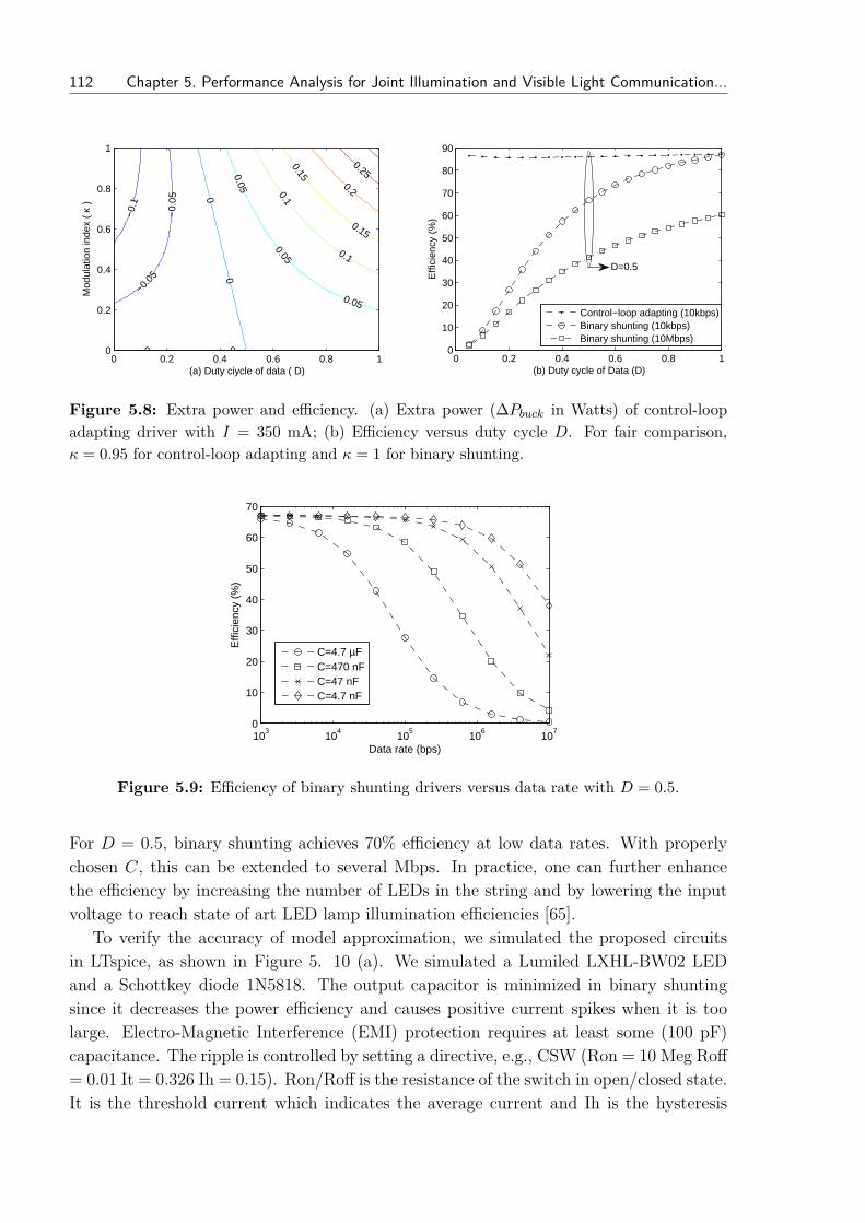
112 Chapter 5. Performance Analysis for Joint Illumination and Visible Light Communication...
−0.1
−0.
05
−0.0
5
0
0
00
0.05
0.05
0.05
0.1
0.1
0.15
0.15
0.2
0.25
(a) Duty ciycle of data ( D)
Mod
ulat
ion
inde
x (
κ )
0 0.2 0.4 0.6 0.8 10
0.2
0.4
0.6
0.8
1
0 0.2 0.4 0.6 0.8 10
10
20
30
40
50
60
70
80
90
(b) Duty cycle of Data (D)
Effi
cien
cy (
%)
Control−loop adapting (10kbps)Binary shunting (10kbps)Binary shunting (10Mbps)
D=0.5
Figure 5.8: Extra power and efficiency. (a) Extra power (∆Pbuck in Watts) of control-loopadapting driver with I = 350 mA; (b) Efficiency versus duty cycle D. For fair comparison,κ = 0.95 for control-loop adapting and κ = 1 for binary shunting.
103
104
105
106
107
0
10
20
30
40
50
60
70
Data rate (bps)
Effi
cien
cy (
%)
C=4.7 µFC=470 nFC=47 nFC=4.7 nF
Figure 5.9: Efficiency of binary shunting drivers versus data rate with D = 0.5.
For D = 0.5, binary shunting achieves 70% efficiency at low data rates. With properlychosen C, this can be extended to several Mbps. In practice, one can further enhancethe efficiency by increasing the number of LEDs in the string and by lowering the inputvoltage to reach state of art LED lamp illumination efficiencies [65].
To verify the accuracy of model approximation, we simulated the proposed circuitsin LTspice, as shown in Figure 5. 10 (a). We simulated a Lumiled LXHL-BW02 LEDand a Schottkey diode 1N5818. The output capacitor is minimized in binary shuntingsince it decreases the power efficiency and causes positive current spikes when it is toolarge. Electro-Magnetic Interference (EMI) protection requires at least some (100 pF)capacitance. The ripple is controlled by setting a directive, e.g., CSW (Ron = 10 Meg Roff= 0.01 It = 0.326 Ih = 0.15). Ron/Roff is the resistance of the switch in open/closed state.It is the threshold current which indicates the average current and Ih is the hysteresis

Part III. Interference Considerations in Visible Light Communication 113
(a)
(b)
Control loop
adaptationBinary
shunting
Figure 5.10: Circuit simulation with BPM waveform in LTspice, using Pout = 1 W bothfor control-loop adaptation and binary shunting: (a) Circuit diagram and (b) LED drivingcurrent. To illustrate the effect of hysteresis control visibly, we use different ripple intensitiesand frequencies.
current which controls the ripple strength. More details on the realization of hysteresiscontrol is outside the scope of this chapter. Figure 5.10 (b) confirms that the current istriangular. The simulated efficiencies when D = 0.5 for these two cases are 84% and 66%,resp., which confirms the accuracy of our approximation model, as shown in Figure 5.8(b) for the two driver designs. To illustrate the effect of hysteresis control visibly, we usedifferent ripple intensities and frequencies. For control-loop adapting, f1 = 100 kHz forA = 150mA. In binary shunting, f1 is adaptively increased to 330 kHz to ensure smallripple of A = 50mA.
5.6.3 Communication performance versus power consumption
In this section, we further illustrate the communication performance in terms of acceptableEEPS (∆E ) and BER, by taking into account the driver efficiency and a total power ofPout = 1 W to deliver a certain required illumination level. For the two drivers, wecompare ∆E versus energy per symbol Es in Figure 5.11. We use D = 0.5 for the bestBER performance for control-loop adapting.
Figure 5.11 confirms that ∆E increases with Es in both drivers. For control-loopadapting, increasing κ increases both Es1 and ∆Es1. In the binary shunting, κ = 1 bydefinition, but we show how both Es2 and ∆Es2 increase with decreasing D until D = 0.5.When D decreases below 0.5, one consumes more power ∆Es2 without improving Es2. Infact, small D implies high peak current level, which lead to excessive power loss. Ourresults quantify the tradeoff between ∆Es2 and Es2. D < 0.5 is not attractive for the

114 Chapter 5. Performance Analysis for Joint Illumination and Visible Light Communication...
0 20 40 60 80 1000
10
20
30
40
50
60
70
80
90
Energy per bit, Es (µJ)
Ext
ra e
nerg
y pe
r sy
mbo
l, E
EP
S (
µJ)
Control−loop adapting (D=0.5, κ∈ (0,1))Binary shunting (D∈ (0,1), κ=1, C=100pF)Simulated for control−loop adaptingSimulated for binary shunting (C=100pF)Simulated for binary shunting (C=470nF)
1
κ0 1
0D
Figure 5.11: Extra energy consumption (EEPS) versus effectively communicated energy perbit (ES) for 1 watt of illumination light (Pout = 1 W) and data rate 10 kbps. 0 κ→ 1 means thatκ is swept from 0 to 1. Similarly, 1 D→ 0 means that D is swept from 1 to 0.
binary shunting. At higher duty cycles, EEPS is nearly proportional to Energy per bit.Further, we see that larger capacitor consume more extra ∆Es2, but only to a limitedextent.
Figure 5.11 shows that for a fixed Es, a driver with an adaptive control loop needsmuch less ∆E than a binary shunting modulator. To study an adaptive control loop,we approximate V0 = V
′0 , that is, we assume that the junction voltage does not change
substantially due to the higher current. Then, Eq. (5.23) becomes
Es1 = V0TsI [κ− (1− 2D)] . (5.47)
Using Eq. (5.21), (5.24) and (5.47), we eliminate κ, to express
∆Es1 = c2[Es1 + V0TsI(1− 2D)]2
V 20 Ts
+ (c1 + 2c2I)(2D − 1) [Es1 + V0TsI(1− 2D)]V0
. (5.48)
For D = 0.5, this simplifies into ∆Es1 = c2E2s1
V 20 Ts
. Although this expression seeminglydoes not depend on κ, the effect of the modulation amplitude is inherently present via thequadratic relation between specified communication energy per bit and the energy neededto achieve that. Moreover, the behavior differs from well-known common intuition in radiocommunication, where one can increase the communication energy per bit either by scalingthe root of the amplitude or the symbol duration, while the consumed energy per bit scalesin the same way as the communication energy per bit. For JIC this is not the case. Infact it is much more energy-efficient to emit longer symbols with (correspondingly) lowamplitude. The resistive losses in the SMPS, in particular the ESR in the magneticscauses this effect. In general, smaller modulation index and larger symbol duration Ts

Part III. Interference Considerations in Visible Light Communication 115
6 6.5 7 7.5 8 8.5 9 9.5 1010
−10
10−8
10−6
10−4
10−2
100
Distance (m)
BE
R
Binary shunting (D=0.5, κ=1)Control−loop adapting (D=0.5, κ=0.69)Control−loop adapting (D=0.5, κ=1)
Figure 5.12: BER versus distance given a power budget of E [Pout(t)] + E [Pbuck(t)] = 2 Watts.
results into a larger ratio of Es1 to ∆Es1. In the limit, for κ→ 0, we have ∆Es1/Es1 → 0,i.e., communication is for free, thus without extra power loss on top of the illumination-only benchmark.
Figure 5.12 allow for system optimization, for a total power budget of 2 W. For D =0.5, the power for illumination is Pout = 2W×85% and Pout = 2W×67% for control-loopadapting and binary shunting, respectively. The efficiency is 85% at 2 Watt, which isslightly lower than the results in Figure 5.8 (b) for 1 W. Control-loop adapting can givea bit stronger illumination than binary shunting, within the same total power budget.
For a fixed power budget (E [Pout(t)] + E [Pbuck(t)] = 2 W), the BER performanceis also compared in Figure 5.12. When D = 0.5 and κ = 1, control-loop adaptingoutperforms binary shunting in terms of a much better BER performance. These twotopologies can have similar BER performance for the specific choice of κ = 0.69 forcontrol-loop adapting.
5.6.4 BER performance with power and ripple consideration
Based on Eq. (5.30), we can avoid a high ripple (i.e, get a small A) by using a largeinductor, a large capacitor and a high PWM frequency f1. In this chapter, ripple ismitigated by setting small threshold gap of the hysteresis control and f1 is increasedadaptively through A = (1 − D)V0/(2Lf1). However, an increased f1 leads to higherswitching losses so it results into a lower power efficiency. Based on the simulation inLTspice, when A = 150 mA, f1 = 100 kHz and when A = 10 mA, f1 = 1.55 MHz. Figure5.13 shows the BER performance for binary shunting with a communication distance of1.5 m, where x-axis is the proposed EEPS and y-axis is the BER. The data rate is 267kbps which is the highest speed for PHY layer I in IEEE 802.15.7 standard.
It is interesting to notice that, the system must tolerate substantial flicker, at the sametime, with a decent BER performance. In another words, decent BER can be achieved

116 Chapter 5. Performance Analysis for Joint Illumination and Visible Light Communication...
0 2 4 6 8 10
10−6
10−4
10−2
100
Extra energy per symbol, EEPS (µJ)
BE
R
A=150mA, f1=100 kHz
A=10mA, f1=1.55 MHz
D=0.5
D00.5
1
0.5
D
Figure 5.13: BER versus EEPS for binary shunting with Pout = 1 W and data rate 267 kbps,comparing low and high ripple intensities. 1 D→ 0.5 means that D is swept from 1 to 0.5 and soon.
at lower energy cost by allowing larger ripple. Similar effect is noticed for control-loopadapting drivers. In Figure 5.13, it is expected that the system has the best BER whenD = 0.5. After that, although Es stays constant as shown in Figure 5.11, the BERdeteriorates due to increased shot noise.
5.7 Conclusion
This chapter analyzed Binary Phase Modulation (BPM) in VLC for an arbitrary mod-ulation depth and duty cycle of the symbols, taking into account signal-dependent shotnoise, power efficiency and imperfections (ripple) of typical LED drivers. In particular,our proposed Delta approximation for the non-Gaussian triangular ripple can well pre-dict the effect of ripple on BER. Ripple interference particularly deteriorates the BERperformance for small modulation depths, significantly, below 10%. Our model and oursimulations show that at deeper modulation depths the effects is modest even for ripplepercentage larger than the modulation depth. Thus, from a power consumption per-spective, one even prefers to tolerate higher ripple levels. However, this may in practicepose some challenges to synchronization and setting the decision thresholds in the re-ceiver, particularly, for direct sampling systems. The ripple interference can be alleviatedfurther by low-pass filtering in the receiver. Two Buck-based LED drivers for BPM areanalyzed and simulated for a practical implementation. Firstly, our proposed control-loopadapting driver can realize high power efficiency. In this case, data rate is constrainedby the frequency of buck self-oscillation PWM frequency but one can increase the PWMfrequency by using a small inductor or adapting the hysteresis levels. Secondly, binaryshunting supports high data rate but that is at the cost of high extra power consump-tion (EEPS). Due to the output capacitor, high data rate can significantly decrease

Part III. Interference Considerations in Visible Light Communication 117
the efficiency of LED drivers. To minimize the effect of capacitor on power efficiency,a small capacitor should be used only for EMI protection in binary shunting. If themodulation frequency increases, in both cases, the switching loss becomes relevant andit also depends on the switch property. In general, our proposed control-loop adaptingdriver outperforms the reported binary shunting one in terms of higher power efficiency,lower EEPS and better achievable BER performance given a power budget. Usually, formany indoor applications where the required data rate is relatively low, the control-loopadapting is attractive for Joint Illumination and Communication (JIC) systems.

118 Chapter 5. Performance Analysis for Joint Illumination and Visible Light Communication...

CHAPTER 6
Reading Analysis for Barcode Scanner with Interferencefrom LED-based Lighting
This chapter is adapted from: X. Deng, P. Zijlstra, Jing Zhang, Y. Wu, G. Zhou and J. P.M. G. Linnartz, ”Performance of barcode scanner using peak detection with interference fromLED lamps,” Communications and Vehicular Technology in the Benelux (SCVT), 2015 IEEESymposium on, Luxembourg City, 2015, pp. 1-6. c©IEEEAnd from: J.P.M.G. Linnartz, Xiong Deng, and Stepahn Nijssen, ”Impact of LED TemporalLight Artefacts on Bar Code Scanners,” Technical Note PR-TN 2016/00117, PHILIPS, 2016.c©PHILIPS LIGHTING HOLDING B.V.
And from: X. Deng, J. P. M. G. Linnartz, K. Arulandu, G. Zhou and Y. Wu, ”Reading Analysisfor Barcode Scanner with Interference from LED-based Lighting,” in submission, IEEE Trans-actions on Industrial Electronics 2018. c©IEEE
Abstract – This chapter addresses the reading failure of a barcode scanner that suf-fers from interferences of Light Emitting Diode (LED) lamps. Barcode scanners can betreated as special communication systems that use light as input. This chapter quanti-fies the reading performance in terms of Timing Signal-to-Interference Ratio (TSIR), inparticular, as a function of modulation depth and frequency of the interference in LEDlighting. The LED interference, generated in the LED driver such as Switched ModePower Supply (SMPS), is neither additive nor Gaussian as discussed in Chapter 5. Thisinterference has a frequency up to several MHz and it seriously affects the barcode readingperformance. To calculate the signal and interference power for TISR, the laser scannerphysical channels are analyzed, including the laser beam path and the LED interferencepath. Since barcode scanners usually use peak or edge detection, the reading reliabilityis subject to the first and second derivative of the LED inference, respectively. We vali-date the proposed TSIR for predicting scanner reading performance by experiments. Forinstance, we found that typical scanners reach a specified sensitivity at a TISR value of
119

120 Chapter 6. Reading Analysis for Barcode Scanner with Interference from LED-based Lighting
around 50. We further investigate the reading performance under multi-frequency inter-ference, e.g. interference from the harmonics of the SMPS control signal. In general, thiswork presents a simple, yet realistic model to quantify the reading performance in termsof TSIR for barcode scanner under sigle-frequency LED interference, and it proposes anempirically verified Flicker Interference Metric (FIM) for multi-frequency interference.
6.1 Introduction
Barcode scanners play an essential role in the electronic data interchange and thus they areextensively used, for instance,in the super market, hospital, express parcel tracking andindustrial production statistics [80]. Meanwhile, as an emerging light source, the LightEmitting Diode (LED) has shown the promise for specialized and general lighting due toits high luminous efficiency, small size, easy control and long lifetime [107]. Nevertheless,this study has found that the rapid fluctuations in LED light output seriously interferewith the barcode scanner, thereby degrading the reading performance. This motivatesus to predict the effect of LED interference on a barcode scanner and, in particular, tounderstand its dependency on modulation intensity (depth) and the repetition frequencyof the LED light output. Since both the modulation depth and frequency are controllablein lighting, they can be potentially optimized to ease risks on equipment that applies lightas input signal such as the barcode scanner.
The barcode scanner evolves from one-Dimensional (1D) to Quick Response (QR) bar-codes preferably with simple and low-cost signal processing techniques. It decodes theinformation from an acquired barcode signal with an accurate estimation of features suchas the edges and peaks of the barcode patterns [91]. For instance, the reported works havedealt with barcode signal for those features using signal filtering [80, 170], waveform anal-ysis [78], deblurring [79], feature extraction [95] and other signal processing techniquessuch as Expectation-Maximization algorithm [43, 180] and Gauss-Newton algorithm [91].However, most of these techniques have not been specifically analyzed under LED inter-ference, since they were initially developed based on the assumption that the noise wasAdditive White Gaussian Noise (AWGN), including the thermal noise, shot noise andspeckle noise [195]. In the scanner, any noise and interference cause a time shift to thezero crossings of a signal intersecting a threshold, namely the timing jitter. Under AWGNnoise, it was proposed that the timing signal-to-noise ratio could determine the readingperformance [16]. Nevertheless, the LED interference is neither additive nor Gaussianand thus its effect on the scanner reading performance needs to be further investigated.To the best of our knowledge, this work presents the first model of a barcode scannersystem that subjects to multiple interferences from the LED lighting.
In particular, most of the reported works analyzed the performance of the barcodescanner based on a convolution of a laser beam over the barcode by considering theoptical channel as constant gain [16, 79, 80]. However, this simplified channel modelis inadequate to analyze the scanner reading performance in practical applications. For
Part III. Interference Considerations in Visible Light Communication 121
instance, the reading distance, which results in a certain channel gain, significantly affectsthe reading performance. Moreover, we found the signal propagation channel is differentfrom the high-frequency LED interference channel. Thus, new channel models are desiredboth for the signal and interference in barcode scanners.
In LED lighting, it is known that the fluctuating LED light potentially imposes riskson human flicker perception [148] and light-based electronic systems such as cameras[93] and barcode scanners [91]. The non-uniform illumination on the target could beperceived by the barcode scanner and thus a joint illumination estimation and deblurringalgorithm was proposed [91]. In contrast to the non-uniform illumination which changesvery slowly compared with the barcode signal, the rapid fluctuations in LED light outputwas further investigated for the barcode scanner [39]. However, practical lighting systemswith multiple interferences were not considered in [39] and no experiment was conductedfor verification. In lighting industry, an International Electrotechnical Commission (IEC)standard with new flicker metrics are still being refined to cover all types of light sources[116], including the emerging LEDs. This also justifies a study into the effect of the LEDinterference on light-based systems such as barcode scanners.
In this chapter, we address the reading failure of a barcode scanner that suffers fromLED interferences. This work has resulted into several contributions. Firstly, we pro-posed new propagation channels for the barcode signal and LED interference separately.We found the received LED interference power by scanner is constant under a requiredillumination level. Secondly, the Timing Signal-to-Interference Ratio (TSIR) was pro-posed and verified for predicting the scanner reading performance under single frequencyLED interference. Thirdly, under a multi-frequency LED interference, a verified FlickerInterference Metric (FIM) was further proposed in the form of P-norm with a weightedfrequency-averaging such that the acceptable barcode reading was enabled. To be specific,we found the TSIR for single frequency interference was not applicable to evaluate thescanner reading performance under multi-frequency LED interference. This is becausemultiple non-AWGN LED interferences results in a combined interference with a compli-cated distribution, in contrast to the AWGN that suggests the same Gaussion distributionfor the combined noise.
To this end, crucial approaches are included in the following sections. A systemdescription of barcode scanner is provided in Section 6.2. The scanner is modeled indetail in Section 6.3. In Section 6.4, barcode signal and the impact of LED interferencewith an arbitrary waveform on barcode reading are analyzed. In Section 6.5, we verifyour model with measurements under single and multi-frequency LED interference.
6.2 System description of barcode scanners
Two classes of scanning technique are widely used in hand-held barcode scanners, in-cluding the light reflection and image capturing. The light reflection scanner is furtherdivided into two subclasses, i.e., LED-pen scanners with manual scanning and 1D laser

122 Chapter 6. Reading Analysis for Barcode Scanner with Interference from LED-based Lighting
Laser
Barcode
UPC code
Interference
500 lux with ripples
PDLED
lamps
Lens
Rotary
prism
Edge or
Peak
Detector Decoded
label
Optical
filterTransmitter Receiver
nt(t)nsh(t)
nsp(t)
Channel
Figure 6.1: Proposed system model for laser scanners.
scanners with automatical sweeping of a laser spot across the barcode. The image cap-turing scanner either uses a camera with an predefined reading line in the image or readthe barcode by using an array detector such as a Charge-Coupled Device (CCD).
This chapter attempts to build a generic model for light reflection scanners such as1D laser scanner. We model it as a communication system that consists of three partsas described in Figure 6.1: 1) a transmitter, which is composed of a laser, lens and arotary prism, 2) an optical path, which includes the reflection against the barcode thatmodulates the spatial code as amplitude time-variations of the beam, 3) and a receiverwhich includes an optical filter, a Photo Diode (PD), an edge detector or a peak detectorand a signal processing module.
The signal disturbances mainly originate from four sources: 1) interference from arti-ficial light such as LED light fluctuation, 2) the thermal noise generated in the receivercircuitry such as the Low-Noise Amplifier (LNA), which is signal-independent, 3) theshot noise, caused by the instantaneous quantum efficiency in the PD, which is signal-dependent, and 4) the speckle noise generated randomly by the rough print of the barcode,which is also signal-dependent [195]. It has been well elaborated in previous works thatthe thermal noise, shot noise and speckle noise were considered as Gaussian noise [195],[18]. However, as non-Gaussian interference, the time-varying (flickering) light outputof LED lamps can severely affect the scanner reading performance, especially when thefrequency of interference is comparable to the scanning rate. Based on our measurement,the LED interference becomes dominant under LED lighting. Thus this chapter is focusedon the LED interference. On the generation of the LED interference in drivers, we referto [36].
In particular, for a laser scanner to operate under ambient light as bright as sunlight,a narrow-band optical filter matching the laser wavelength is often desired [71]. Nonethe-less, due to the wide spectrum of white light, some parts of the light still reach thephotodetector as shown in Figure 6.2. Moreover, the cool light has more power enteringinto the scanner than warm light due to the higher spectrum at the the laser wavelength.Note that, the high performance optical filter is hardly used in the barcode scanner dueto its high cost. In genaral, different from the constant sunlight which can be simplyfiltered out as DC in the receiver, the fluctuating LED output light becomes a seriousinterference to barcode scanner and thus affects the scanner reading performance.

Part III. Interference Considerations in Visible Light Communication 123
350 400 450 500 550 600 650 700 750 8000
0.2
0.4
0.6
0.8
1
1.2
Wavelenghth (nm)
Rel
ativ
e po
wer
Typical spectral power distribution of white LED
Phosphor warm whitePhosphor neutral whitePhosphor cool whiteIdeal red laser filter
Figure 6.2: Typical spectral power distribution of white LED and red laser filter with centerwavelength at 633nm and bandwidth of 10nm .
In general, a barcode scanner with fast scan velocity and large depth of field of theview is desired. Nevertheless, the scan velocity is constrained by the transmitted powerwhich is limited by the eye safety. The scan depth is mainly affected by the blurringthat is caused by the convolution process of the laser spot over the barcode symbol. Thiswork proposes a performance metric, i.e., TSIR, by taking into account all the relatedparameters such as the laser power, scan velocity and reading depth.
6.3 System model for laser scanners
In this section, the transmitter, channel and receiver of the laser scanner shown in Figure6.1 are discussed in detail. In particular, new channel models are proposed to calculatethe received signal and interference power.
6.3.1 Transmitter
As shown in Figure 6.1, the laser is the signal source in the transmitter. The outputlaser beam is concentrated by an optical lens, then reflected by a rotary mirror, and atlast it scans across the barcode. In particular, using the microelectromechanical systems(MEMS), the laser beam can be steered without a mechanical motor in the transmitter[66], which leads to a compact and low-cost barcode reader. In such case, the traditionalchannel model for mechanical scanners is not applicable and thus new channel models arenecessary.
6.3.2 Channel
Unlike most of communication systems using the Light-of-Sight (LOS), the scanner de-tects information that is embedded in the barcode through the reflected path betweenthe transmitter and the receiver.

124 Chapter 6. Reading Analysis for Barcode Scanner with Interference from LED-based Lighting
Laser
Ae
Detector
Al
r
Infinite edge
Figure 6.3: Signal propagation channel of the barcode reader.
6.3.2.1 General channel modelThe scanner uses a laser to illuminate a small area within the printed barcode. Thedetector collects the reflected light and sees a temporal waveform when the spot is scannedacross the barcode. The propagation path is illustrated in Figure 6.3. The effective areaAe that the receiver can observe is usually designed to be larger than the laser spot sizeAl and also larger than the barcode, but preferably not too large, to avoid the collectionof unwanted noise or interference.
From Figure 6.3, the received optical power Ps from the laser at the detector is ex-pressed as
Ps =∫λPlaser(λ)LL−PR(λ)LP−DF (λ)dλ, (6.1)
where Plaser(λ), LL−P and LP−D are the output power spectrum of laser over the wave-length λ, the loss from laser to paper and the propagation loss from paper to the detector,respectively. Sine all laser power falls in the spot area, we have LL−P = 1 and thus theoptical power in the spot is independent of the distance d between the laser source andthe barcode. The laser signal is reflected by the barcode with a reflection coefficient R(λ).Then it passes through the optical filter F (λ) and finally it is picked up by the PD. Here,the path loss LP−D between the paper and the detector depends on d.
6.3.2.2 Propagation channel of the laser beamThe simplified channel model for laser signal is proposed in Figure 6.4 (a). The laser beamis rotated by the MEMS micromirror that utilizes a magnetic actuation. Specifically, anelectric current flowing through the mirror to generate an equivalent mechanical scansacross the barcode. The scattered light is received and then focused by a compound lensonto the PD. The laser signal is attenuated by the optical path from paper to detector.
The optical configuration using a MEMS micromirror in the scanner typically has alarge detection area and thus it is sensitive to the noise and interference. The reflectionfrom a paper surface is well approximated by a Lambertian radiation [195]. We writethe Lambertian reflection as R (φ) = [(m+ 1) /2π] cosm (φ), where φ is the angle betweenthe outgoing laser beam and the main lobe direction of the refection pattern [51]. The

Part III. Interference Considerations in Visible Light Communication 125
MEMS
micromirror
Lambertian
radiation
Photodiode
ᶲ
Laser
Compound lens
d
θ
Barcodel
Photodiode
View angle
d0
Ae
0
Lambertian
radiation
'
'
r
(a) Laser beam propagation channel (b) Interference propagation channel
Figure 6.4: Optical configuration of a barcode reader with MEMS.
order m can be calculated by m = −ln2/ln(cosΦ1/2
), where Φ1/2 is the semi-angle at
half power of the pattern. For instance, the measured semi-angle of the pattern for acardboard is around 30 [195]. Thus the propagation loss from paper to the detector is
LP−D = Ad cos θR(φ)d2 = Ad cos θ(m+ 1)cosm(φ)
2πd2 , (6.2)
where Ad is effective aperture of the PD considering the effect of compound lens. Theangle θ is the off-axis angle in the normal direction of the lens and in such case, φ = 2θ.The lens is located in a distance d from the laser spot. After the lens, the received opticalpower by PD is converted into current IPD, expressed as
IPD = εPs = εPlaserR(λ)Ad(m+ 1)cosm(φ) cos θ2πd2 , (6.3)
where ε is the PD responsivity (A/W) and Plaser =∫λ Plaser (λ)F (λ) dλ is the received
power after the integration over wavelength λ, with assumption that reflection coefficientR(λ) is independent of λ. Since the electric power takes square of the current, the signalpower declines according to the fourth power of distance d. Except for the signal powerloss, in Section 6.4.1, we further investigate the signal dispersion that depends on thespot size and the scan distance (depth).
6.3.2.3 Propagation path of the LED interferenceThe LED interference was considered as a self-influence in a VLC system [36]. In thischapter, the fluctuation of the LED output light becomes a cross-interference into otherlight-based systems, for instance, barcode scanners. In scanner systems, the propagationpath of LED interference is quite different from that of the laser beam.
The barcode and its surrounding environment are simultaneously illuminated by theLED lighting. Specular reflection is less likely for the LED interference because the light-ing is typically designed to avoid glare. Thus the illumination is realistically modeled tobe uniform. Hence, we model the reflected light interference from the paper as Lamber-tian radiation with a main lobe perpendicular to the paper surface, as shown in Figure 6.4

126 Chapter 6. Reading Analysis for Barcode Scanner with Interference from LED-based Lighting
(b). In particular, since the far field effect for the Lambertian radiation, the interferenceis represented by the accumulation of a large number of small radiation elements.
As illustrated in Figure 6.4 (b), the interference power received from the LED lightcan be expressed as an integral over the effective area Ae and the wavelengths. So, wehave
nLED =∫∫
Ae
∫λPLED(λ)PP−D(a, b)F (λ)rdrdβdλ, (6.4)
where PLED(λ) is the Power Spectral Density (PSD) of LED output light. The powerloss PP−D(a, b) is caused by the Lambertian re-radiation at (a = r cos β, b = r sin β) foreach small spot in the view area, thus
PP−D(r cos β, r sin β) = Ad cos θ′(m+ 1)cosm′(φ′)2π(d2
0 + r2) , (6.5)
where d0 is the vertical distance from paper to the detector. Because the main lobe isperpendicular to the paper surface, we have φ′ = θ′. If assume that all patterns have m′= 1, integrating over the whole area, the total received interference power nLED becomes
nLED = PLED
∫ d0 tan θ0
0
Add20
π(d20 + r2)2 rdr
∫ 2π
0dβ
= PLEDAdtan2θ0/
(1 + tan2θ0), (6.6)
where θ0 is the view angle of the barcode scanner. PLED =∫λ PLED(λ)F (λ)dλ is the light
density on the scanned area, expressed as W/m2. From Eq. (6.6), it can be concluded thatthe interference from LED nLED is always constant given the view angle and illuminationlevel.
We define electrical SIR = (εPs/εnLED)2 as the signal to interference ratio. Based onEq. (6.3) and (6.6), provided that LED flicker interference was solely present, the SIRalso declines according to a fourth power of distance d and it is expressed as
SIR =(PlaserR(m+ 1)cosm(φ) cos θ(1 + tan2θ0)
2PLEDπd2tan2θ0
)2
. (6.7)
It is necessary to note that, the scanner reading performance is not determined by theSIR since it does not take into account the scan rate. Thus a new metric in terms ofTSIR is provided in Section 6.4.
6.3.3 Receiver
As mentioned before, there are two widely used barcode detection algorithms for barcodescanner, i.e., the edge and peak detection [80]. These two algorithms are also widely usedin other applications such as image processing [21], [176].

Part III. Interference Considerations in Visible Light Communication 127
CPU
Decoder
Zero
CrossingDecoded
label
n(t)r(t)
d
dt
2 2
22
I d
dt
Low-pass
Filter
HG(w )-
s(t)
( )s t
( )n tInverse
Filter
Figure 6.5: Peak detection for laser scanners.
CPU
DecoderDecoded
label
d
d t
d
d t
And
And
Set
Reset
V+
V-
Enhancement
Filter
Hf(w)n(t)r(t)
( )s t
( )n t
Figure 6.6: Edge detection for laser scanners.
6.3.3.1 Peak detectionFigure 6.5 shows a peak detection implementation for barcode reading, using the 1stderivative [80]. The zero crossing of the 1st derivative of signal is used to find the peak orvalley of the received signal, which corresponds to the midpoint of the modules (stripesand gaps) of the barcode. Note that, the 1st derivative is calculated after the low-passfiltering to suppress the wide-band noise. For deburring the signal, a further scaled secondderivate is needed based on the inverse filter design. This method is mainly used for highdensity barcode, i.e., σl < Tb < 4σl, where σl is a quarter of the spot size of the laserbeam in time and Tb is the module duration of the smallest bar or space.
6.3.3.2 Edge detectionThe zero crossing of the 2nd derivative of the received signal can indicate the edge ofthe barcode. The implementation of edge detection using the 2nd derivative is shownin Figure 6.6. In this scheme, after the signal and noise passing through a enhancementfilter, the second derivative is computed for edge locations while other signals are alsoinvolved to avoid false edges. The edge detection is usually used for a low density barcode,i.e., 4σl < Tb. More details can be found elsewhere [18].
6.4 Signal and performance analysis for laser scanners
6.4.1 Signal description
The scanning with velocity v transfers the barcode from space domain to time domain[118]. Normally, the scanning process is modeled as a one-dimensional along the x direc-tion, although the laser spot is 2D [13], [173], [170]. Thus we model the scanning processas the convolution of the laser spot over the barcode with additive noise n(t), so the

128 Chapter 6. Reading Analysis for Barcode Scanner with Interference from LED-based Lighting
received signal r(t) is
r(t) = εLP−DX(t)⊗ h(t) + n(t), (6.8)
where X(t) is the reflectivity function of the barcode in time and h(t) indicates thelaser Point Spread Function (PSF) of the optical system. h(t) is generally modeled by aGaussian function to produce the edge response [8] [195], expressed as
h(t) = Ap1√
2πσlexp(−t
2
2σ2l
), (6.9)
where Ap is the power of the laser beam. σl is the temporal spread expressed as σl =w/ (4v), where w is the diameter of the laser spot. As elaborated in studies [80], [121], thelaser beam converges to a non-zero minimum waist diameter w0 and then spreads witha divergence angle α = 4λ/πw0 to the far-field region, typically α < π/180 (1 degree).Since w0 is very small, the beam diameter can be described as w = 2dtanα. So the laserpoint spread and the corresponding parameter σl grows when the barcode is moved awayfrom the scanner. To ensure proper decoding, the spot size preferably is smaller than thewidth of the barcode module to decrease the convolution distortion while it also shouldbe reasonably large to avoid amplification of print imperfections.
Due to the scanning velocity v, X(t) is described as
X(t) = C
2
n−1∑i=0
(−1)iU(t− ti) + Rw +Rb
2 , (6.10)
where ti = xi/v and xi is the edge location in space. The Rw and Rb are the reflectanceof the spaces and bars respectively. C = Rw − Rb is the print contrast ratio or, moreprecisely, the reflectance difference between the bar and space. U(t− ti) is the unit stepfunction at the transition point ti.
6.4.2 Signal enhancement
During scanning, the Gaussian PSF acts as a Low-Pass Filter (LPF) to ”smear” thesignal. A high-pass inverse filter is usually used for deblurring the convolution distortion,which enhances the signal [80]. The inverse filter will also enhance the high frequencynoise and thus another low pass filter is applied but with a cut off frequency above thesignal spectrum [16], [170]. To combine these filters, we firstly model the inverse filter asa series expansion
HI(ω) = exp(ω2σ2I/2) = 1 + ω2σ2
I/2 + ω4σ4I/8 + · · · , (6.11)
where σI = ησl and usually the scaler η is 1. Since σI is quite small, we can use secondor fourth-order polynomial to approximate the series in the relevant ω range.

Part III. Interference Considerations in Visible Light Communication 129
6.4.2.1 Peak detectionAs shown in Figure 6.5, the second-order polynomial HI(ω) = 1 + ω2σ2
I/2 is used toapproximate the high-pass inverse filter in Eq. (6.11) and then σI is optimized to avoidexcessive noise enhancement above certain frequency. For the LPF HG (f) in Figure 6.5,we further use a Gaussian LPF which has the same form as the laser spot [154], [17].Thus, the transient response of HG (f) is expressed as
hG(t) = 1√2πσf
exp(−t2
2σ2f
), (6.12)
with Fourier transform HG(ω) = exp(−ω2σ2f/2) and σf indicating its bandwidth which is
optimally selected for a typical scan distance.
6.4.2.2 Edge detectionFor edge detection, an edge-enhancement filter is proposed [170], which combines thenoise limiting and deblurring in one filter design. This filter can be described by the ratioof two polynomials as
Hf2(s) = B(s)/A(s), (6.13)
where the numerator of B(s) = 1− s2σ2I/2 + s4σ4
I/8 is used to approximate the prototypeof the inverse filter in Eq. (6.11) using s parameter. The sixth-order Bessel filter was usedfor the denominator since it has a low-pass property with a linear phase but no overshoot[170]. However the drawback of the Bessel filter is that its response is not as steep as theGaussian low-pass filter. Thus for better comparison, the same low-pass Gaussian filterin Eq. (6.12) is applied for edge detection.
6.4.3 Signal for peak and edge detection
This chapter focuses on the analysis for peak detection using the first derivative. Afterthe low-pass filter in Figure 6.5, the barcode reader calculates the first derivative s(t) todigitalize the received signal r(t) [18, 24, 80] such that
s(t) = GS
2
[n−1∑i=0
(−1)i 1√2πσo
exp(−(t− ti)2
2σ2o
)], (6.14)
where GS = εLP−DApC indicates the signal channel gain. And σ2o = σ2
l + σ2f is the total
blurring. Considering the effect of the inverse filter, the signal used for peak detection is
sf (t) = s(t)− σ2Is′′(t)
/2. (6.15)

130 Chapter 6. Reading Analysis for Barcode Scanner with Interference from LED-based Lighting
In edge detection, the edge is mathematically determined by the second derivative ofthe received signal r(t). The detailed analysis for edge detection is omitted to avoid rep-etition since similar approach can be applied, but its results are depicted for comparisonin Section 6.5.
6.4.4 Received interference from LED
The interference of AC-driven LED often has a strong 100 Hz (or, in USA, 120 Hz)component, but it is less harmful to barcode scanner. However, LEDs are usually poweredby SMPS in efficient lighting [186]. In such case, the SMPS injects a cyclostationaryintensity modulation with a frequency of at least several kHz, but often above 20 kHz toavoid any risk of audible noise coming from inductors in the lamp. More seriously, thefrequency can be several MHz by taking into account the harmonics.
6.4.4.1 Interference in SMPSIn this work, the SMPS is considered due to its high power efficiency and easy digitalcontrol. Depending on the application, the topology of SMPS could be based on basicbuck, boost and Cuk converter [182]. For instance, the buck-based SMPS works as a DCto DC converter for high to low voltage conversion. However, it incurs a triangular ripplewhose frequency depends on the Pulse-Width Modulation (PWM) control signal [36]. Itis necessary to note that there is a tradeoff between efficiency and the ripple suppressing,in other words, a high efficiency SMPS has substantial current ripples.
Usually, an output capacitor is necessary for ripple suppression in SMPS. However, thecapacitor still leaves the fundamental frequency and its harmonics. In barcode scannersystem, low-frequency harmonics of LED interference affect the reading performance.Therefore we initially model the LED light output pl(t) with a sinusoid waveform andwrite for a single-frequency interference as
PLED(t) = pl(t) = plDC [1 + κ sin(ωt)] , (6.16)
where p is the scale factor that indicates the transformation from irradiance to opticalpower [136], lDC is the light level at the reading pane, typically with 500 lux, and ω isthe frequency of the interference.
The modulation depth κ (0 < κ < 1) in LED lamp is defined as the output lightdifference divided by the sum of the two light levels,
κ = (lmax − lmin)/(lmax + lmin), (6.17)
where lmax, lmin are the highest and lowest illumination levels in Lux. Although insome cases the interference waveform does not exactly resemble a sinusoid, the followingapproach still applies after the Fourier transformation.

Part III. Interference Considerations in Visible Light Communication 131
For peak detection, we detect the zero crossing of the first derivative. Based onEq. (6.6) and (6.16), the interference n1(t) seen at the detector can be interpreted as arandomly phased periodic signal
n1(t) = d
dt
[εnLED(t+ ξ)⊗ hG(t)⊗ hI(t)
]= GIH0(ω)κω cos(ωt+ ξ)
, (6.18)
where GI = εAdplDCtan2θ0/(1 + tan2θ0) is the interference channel gain, ξ describes therandom phase offset of the LED flicker and hI(t) is the impulse response of the inversefilter. H0(ω) = HG(ω)HI(ω) indicates the overall filter response.
6.4.4.2 Statistical model for sinusoidal interferenceThe mean of n1(t) can be expressed as
µLED = En1(t) =∫ T
0n1(t)p(ξ)dt = 0, (6.19)
where p(ξ) = 1/T indicates the uniform distribution of the phase in one period. Thevariance of n1(t) can be expressed as
σ2LED = En1(t)2 − E2n1(t) = [GIH0(ω)κω]2
/2. (6.20)
For the sinusoidal interference, the probability density function of n1(t) can be ex-pressed as [36]
fLED(n1) =
1
π√ρ2LED−n
21, for |n1| < ρLED
0, elsewhere, (6.21)
where the electrical signal amplitude ρLED = GIH0(ω)κω linearly depends on the powerloss of the interference. Exact calculation of the error probability (per peak detection)becomes complicated, but a binomial approximation will be considered, with
fLED(n1) = a1δ (n1 − ρ1) + a2δ (n1 + ρ2) , (6.22)
where ρ1 = ρ2 = ρLED and a1 = a2 = 1/2.In particular, most of SMPSs produce a triangular interference waveform. In such
case, a1 and a2 become the fractions of time in the rising and falling ramp, respectively.In addition, ρ1 and ρ2 are the slope of the rising and falling ramps, respectively.

132 Chapter 6. Reading Analysis for Barcode Scanner with Interference from LED-based Lighting
-5 -4 -3 -2 -1 0 1 2 3 4 5-5
-4
-3
-2
-1
0
1
2
3
4
Times
tii=(i+0.5)Tb
1( )iin t
'arctan ( )f iis t
' ( )fs t
'
1( ) ( )fs t n t
Figure 6.7: First derivative with zero crossing time and sinusoid interference.
6.4.5 Error models
This chapter analyzes the effect of the LED interference for peak detection using thefirst derivative. The zero-crossing time of the first derivative becomes uncertain due tosinusoidal interference. In Figure 6.7, without interference, the ith zero-crossing point attime tii = (i + 0.5)Tb indicates the barcode midpoint. The time module is expressed asTb = SM/v, where SM is the size of barcode module. However the interference shifts thezero-crossing point to time tii + ∆, where ∆ is the amount of timing shift, namely timingjitter [16]. As illustrated in Figure 6.7, the time shift ∆ can be expressed as
∆ = n1(tii)/sf ′(tii), (6.23)
where n1(tii) is the LED interference and s′f (tii) is the slope of the signal sf (t) at thesame ith zero-crossing point tii.
For a single zero-crossing point, the error probability that the interference plus noiseexceed a certain threshold εTb (ε = 0.5) equals the (two-sided) probability that point isshifted into an erroneous quantization zone. Hence the error probability is expressed asthe sum of two equal error probabilities
Perr 1 (|∆| ≥ εTb) = Perr 1(|n1(tii)| ≥ εTbs
′f (tii)
)= 2
∫ ∞εTbs
′f
(tii)fLED(n1)dn1
. (6.24)
6.4.5.1 Binomial approximationIf we use the binomial approximation for fLED(n1) in Eq. (6.22), we get
Perr 1 =
1, if |ρ1| ≥ εTbs′f (tii)
0, if |ρ1| < εTbs′f (tii)
, (6.25)
which means that, once the timing jitter exceeds the threshold, the scanner fails to readthe barcode information. Thus when multi-frequency interference are present, the readingperformance is mainly determined by the strongest component.
Part III. Interference Considerations in Visible Light Communication 133
6.4.5.2 Gaussian approximationIf we make additive and Gaussian approximation for the LED interference, Eq. (6.24)becomes,
Perr 1 = 2√2πσLED
∫ ∞εTbs
′f
(tii)exp( −n
21
2σ2LED
)dn1
= erfc(√
TSIR/
(2√
2)) , (6.26)
where erfc(.) is the complementary error function and we define TSIR as
TSIR =[Tbs′f (tii)
]2/σ2LED. (6.27)
In particular, the additive and Gaussion approximation indicates that the effect ofmulti-frequency interference on reading performance is determined by the summation ofthe power in each frequency component .
6.4.5.3 Error bound and TSIRMore generally, for any probability density function of n1(t), Chebyshev’s inequality givesus the upper bound
Perr 1 (|∆− µ∆| ≥ εTb) ≤σ2
∆
(εTb)2 = 1ε2TSIR
, (6.28)
where the mean of timing jitter µ∆ = 0 and its variance σ2∆ can be calculated from Eq.
(6.20) and (6.23). Eq. (6.28) suggests that the upper bound only depends on the value ofTSIR. For single-frequency interference, it is expected that the probability of a barcodescanner error depends on the TSIR. Thus, we use TSIR as a reading performance metricfor scanner under single-frequency interference.
Based on Eq. (6.14), (6.15), (6.20) and (6.27), we calculate the TSIR at tii = (ti +ti+1)/2. For simplifying the calculation, we start with the first midpoint at t00 = (t0 +t1)/2. From Eq. (6.15), the first part of s′f (t00)
s′(t00) = GS
2
[n−1∑i=0
(−1)i−(t00 − ti)√2πσ3
o
exp(−(t00 − ti)2
2σ2o
)]
≈ −GSTb
2√
2πσ3o
exp(−(Tb)2
8σ2o
), (6.29)
where we assume σo < Tb < 4σo for the high density barcode and thus the effect of ti≥2
on s′(t00) is negligible. Similarly, we get the second part of s′f (t00). At last, a general

134 Chapter 6. Reading Analysis for Barcode Scanner with Interference from LED-based Lighting
expression for sf (t) at tii = (ti + ti+1)/2 is achieved as
s′f (tii) = s′(tii)−σ2I
2 s′′′(tii)
≈ GS
2 exp(−(Tb)2
8σ2o
)− Tb√
2πσ3o
− σ2I
2
[3Tb√2πσ5
o
− (Tb)3
4√
2πσ7o
]
≈ GSTb
2√
2πσ3o
exp(−(Tb)2
8σ2o
)(−1− 3σ2
I
2σ2o
) , (6.30)
where the approximation is reasonable since the third order of Tb is very small. So theTSIR becomes
TSIR ≈
GSS3M
(−1− 3σ2
I
2σ2o
)16√πGIR3
stan3(θ0)σ3o
2 exp(−D
d20)
d30κωH0(ω)
2
, (6.31)
where D = (2ηSMcosθ/tanα)2/8. From Eq. (6.31), the TSIR decreases with the fre-quency ω and modulation depth κ of interference from the LEDs. Especially, the totalblurring σ2
o is independent with distance d0. Compared to the SIR in Eq. (6.7), we caneasily find that the TSIR declines approaching to a sixth power of distance d0, which isdifferent from communication channels.
6.5 Experimental validation
In this section, we present numerical results of the proposed TSIR with different dis-tance, frequencies and modulation index of the LED light interference. Moreover, for arequired detection error probability with a given TSIR value, the tolerable modulationdepth (sensitivity) under single-frequency LED interference is calculated and validatedby experiments. Finally, since the LED interference is non-addictive and non-Gaussian,a new metric in terms of Flicker Interference Metric (FIM) is proposed and verified toestimate the effect of the multi-frequency LED interference.
In this chapter, the sensitivity of the barcode scanner is measured in a room that isilluminated only by LED lighting. The experimental setup includes LED lamps, a barcodelaser scanner, a signal generator, an amplifier, a lux meter and a photo detector connectedto an oscilloscope, as shown in Figure 6.8. A sinusoidal signal is initially generated andamplified. Along with a DC power, the DC-biased sinusoid signal feeds the LED lamps.The lux meter measures the LED light level that reaches the barcode, and the oscilloscopewith the photo detector measures the light waveform and modulation depth of the LEDinterference. In particular, to improve the reliability of the experiment, eight UniversalProduct Code (UPC) barcodes are placed on a turntable which has a constant speed.Using this turntable, the scanner reads the barcodes with the same scan time for each

Part III. Interference Considerations in Visible Light Communication 135
Signal Generator
Amplifier
LED Lamps
Photo Detector
Oscilloscope
Barcode
Interference
Motorola LSXXXX
Lux Meter
LED Lamps
MotorolaLSXXXX
Photo Detector
Oscilloscope
Barcode on Turntable
Lux Meter
Figure 6.8: Measurement scheme and setup.
0.2 0.4 0.6 0.8 110
−1
100
101
102
103
104
105
Distance(m)
TS
IR
TSIR versus distance
Theoretical4th power of d
0
6th power of d0
Figure 6.9: TSIR versus distance.
barcode. When the turntable rotates for a round and two of the eight barcodes fail tobe recognized, the scan error probability is 25% and the corresponding modulation depthis considered as the sensitivity. Unless otherwise stated, the related parameters used forthe calculation and setup are listed in Table 6.1.
6.5.1 TSIR
Figure 6.9 shows the numerical results of TSIR versus distance and we compare the TSIRwith its approximation using the 4th and 6th power of d0 in the denominator of Eq. (6.31).As we can see, during a short scan distance, the TSIR is quite small due to the dominanteffect of the exponential term in Eq. (6.31). When increasing the scan distance, there isan optimal distance around 20cm with the largest TSIR and many barcode scanners aredesigned for this distance. After that, the TSIR declines approaching to the inverse ofthe sixth power of distance other than the fourth power.
Based on Eq. (6.31), we can express TSIR in terms of other parameters that weare interested in, e.g., the frequency and modulation index of the LED interference. As

136 Chapter 6. Reading Analysis for Barcode Scanner with Interference from LED-based Lighting
Table 6.1: Parameters for barcode scanner and setup
Parameter Interpretation Valueε Responsivity of the PD 0.5 A/WC Print contrast of the barcode 0.8Plaser Laser power complied with IEC standards 1 mWAd Effect aperture of PD 100 mm2
SM UPC-A module size with 100% manifest 0.3 mmθ0 View angle of the barcode scanner 30 degreeθ Off axis angle of the laser spot 3 degreeΦ1/2 Semi-angle at half power of laser pattern 30 degreeφ Off axis angle of PD 2θα Spread angle of the laser beam 0.04 degreed0 Distance between reader and distance 20 cmη Scaler for inverse filter 1Rs Scan rate of the reader 100 c/slDC Typical illumination level 500 luxp Scale factor of irradiance to optical power 10−3
expected, the scanner system has a larger TSIR value with a smaller modulation depthκ [39]. For TSIR versus frequency, we notice there is a valley around 150 kHz caused bythe electronic low-pass filter. To be specific, below 150 KHz, the TSIR decreases withincreasing the interference frequency. This is because the low frequency interference canpass through the electronic filter and affects the system. But after that, the low-passfilter attenuates the high-frequency component gradually and thus the system becomesimmune to high-frequency interference.
6.5.2 Sensitivity versus frequency
Given a required detection error probability, the tolerable modulation depth (sensitiv-ity) under single-frequency LED interference is measured by gradually increasing thefrequency and changing the modulation index of the interference. For error probabilityof 25%, the measured tolerable modulation depth is shown in Figure 6.10, where x-axisis the interference frequency and y-axis is the tolerable modulation depth. Since thescan error probability is determined by the TSIR, the predicted sensitivities for differentTSIR values are also depicted in Figure 6.10. As we can see, the predicted sensitivityfor peak detection with TSIR = 50 agrees well with the measurement.
For TSIR = 50, the frequency, where the scanner with peak detection starts to beaffected by the LED interference, is around 1 kHz. Further increasing the interferencefrequency until to 150 kHz, the tolerable modulation depth decreases and this means thescanner becomes more sensitive to the interference. After the most sensitive point around150 kHz, the scanner gradually becomes immune to the high frequency interference due

Part III. Interference Considerations in Visible Light Communication 137
100
102
104
106
10−3
10−2
10−1
100
Frequency (Hz)
Mod
ulat
ion
inde
x κ
Tolerable modulation index versus frequency
Peak Detection with TSIR=50Peak Detection with TSIR=100Peak Detection with TSIR=200Edge Detection with TSIR=50Measurement
Figure 6.10: Tolerable modulation depth versus frequency.
to the low-pass filter. Similar effects are found for different TSIR values. In particular,a larger TSIR value indicates a lower scan error probability. However, for larger TSIR,the scanner is more sensitive to the modulation depth or light fluctuation. Thus there isa tradeoff between the light fluctuation tolerance and the probability of correct reading.
For edge-detection scanner using the same system parameters, the predicted tolerablemodulation depth with TSIR = 50 is depicted for comparison. The predicted sensitivityindicates that the edge-detection scanner starts to fail around 15 kHz which is higherthan that of peak detection. This confirms that the edge detection is more tolerable thanpeak detection in low-frequency band. Since the TSIR of edge detection declines withthe second power of frequency, the tolerable modulation depth drops very fast and gets avalley around 210 kHz. At this most sensitive frequency, a very small fluctuation in LEDlighting causes failure in reading the barcode.
The threshold TSIR for the measured results is further shown in Figure 6.11. Thethreshold TSIR is expected to be a constant but it fluctuates between 27.5 and 146.5 inthe measurement, which is caused by the limited resolution of test. For the worst case,the threshold TSIR should be at least 146.5 for a required scan error probability. Basedon this value, the required modulation depth in lighting design is then determined.
6.5.3 Sensitivity under multi-frequency
It is important to verify the sensitivity under multi-frequency LED interference becausethe light fluctuation due to SMPS typically contains multiple harmonics. Moreover, thelighting system usually has different types of LED lamps and thus the LED interferencecan have different frequency components.
The expression in Eq. (6.24) for error probability suggests that we need to investigatethe probability density function of the multi-frequency LED interference, which howeverusually becomes intractable. On one hand, the Gaussian approximation proposed in Eq.

138 Chapter 6. Reading Analysis for Barcode Scanner with Interference from LED-based Lighting
104
105
20
40
60
80
100
120
140
160
180
200
Frequency (Hz)
TS
IR th
resh
old
TSIR threshold versus frequency
MeasurementTSIR=27.5TSIR=146.5
Figure 6.11: Threshold TSIR versus frequency.
(6.26) suggests that we may sum up the powers of the individual components. Neverthe-less, such assumption is unrealistic for the LED interference which is non-additive andnon-Gaussian. On the other hand, our binomial approximation for a sinusoidal or trian-gular interference, which contains multiple harmonics of a fundamental frequency, wouldsuggest that the biggest power of the individual components may matters.
Experimentally, the sensitivity under multi-frequency interference is investigated byusing two frequencies of 2 kHz and 10 kHz. These two frequencies with odd-multiplerelation are inspired by the harmonics in typical SMPS, which belongs to the Fourierseries expansion of a triangular waveform. In the measurement, the signals at these twofrequencies are synchronized at the beginning, which results into the worst case withpotential peak modulation depth. Thus, it provides the bound limit for other randomphases. With a predefined modulation depth of the 2 kHz light, the modulation depthof the 10 kHz light is gradually changed until the mixed light reaches the sensitivitypoint for the scanner. Then the modulation depth is recorded. The measured results andnumerical results for a mixture of the two frequencies are shown in Figure 6.12, wherethe x and y axes are normalized by their single-frequency sensitivity, respectively.
From this figure, the ratios of the two lights approximately fulfil nf1 + nf2 = 1, wherethe ratio nf1, nf2 are defined as the ratio of actual modulation depth κf1,2 over thetolerable modulation depth for each frequency κf1,2 th (see Figure 6.10), e.g., n2kHz =κ2kHz/κ2kHz th. In particular, we found that it is a generic relation since it holds for othergiven TSIR valves. Thus when different types of LED lamps have the same illuminationlevel (white light) or equally one lamp has multi-frequency flicker components, the effectof multiple-frequency interference is captured in a generic formula and thus a new Flicker

Part III. Interference Considerations in Visible Light Communication 139
0 0.2 0.4 0.6 0.8 10
0.2
0.4
0.6
0.8
1
Ratio of modulation depth for 2 kHz
Rat
io o
f mod
ulat
ion
dept
h fo
r 10
kH
z
Sensitivity under multi−frequency interference
p=1p=2p=1.5Measurement
Figure 6.12: Sensitivity under multi-frequency interference.
Interference Metric (FIM) is proposed as
FIM = p
√√√√∑∞m=1
(κfmκfm th
)p< 1 not influential= 1 just influential> 1 influential
, (6.32)
where p is the norm factor and m indicates the mth frequency component. The sensitivityfor FIM = 1 with different p are shown in Figure 6.12. As we can see, if the LEDinterference is best described by the AWGN approximation which related to the peak-to-peak power of the interference, an appropriate choice would be p = 1 (45 degree line);if the rms value of the ripple is mostly relevant, p = 2 (circle); and if only the largestripple component is relevant based on the binomial approximation, x approaches infinity(enclosing box). We conclude that linear weighing factor (p = 1) underestimates thedistance by LED interference and the rms weighted amplitude overestimates it. Howeverbased on the measured results, the p = 1.5 would be a reasonable and empirical weightingfactor. In particular, interferences with any random phases should locate in the rangebetween p = 1 to p = 1.5.
6.6 Conclusion
This work analyzed the reading performance of barcode scanners under the LED in-terference in terms of Timing Signal-to-Interference Ratio (TSIR) instead of Signal-to-Interference Ratio (SIR), since the SIR does not take into account the scanning rate.To this end, this chapter initially investigated the different propagation channels for thesignal and interference in barcode scanners separately. Then based on the decoding algo-rithm, we derived the TSIR, which declined approaching to the inverse of the 6th power ofthe reading distance. Moreover, for a given illumination level in lightning, the amount oflight interference falling into the scanner was constant and there was an optimal distance

140 Chapter 6. Reading Analysis for Barcode Scanner with Interference from LED-based Lighting
around 20 cm for barcode scanner reading. Besides, as expected, the reading performancehighly depended on the modulation depth and frequency of the LED interference. Formulti-frequency interference, we proposed a new metric FIM with 1 ≤ p ≤ 1.5 in lightingdesign to enable scanner reading. We expect that our work can be extended to predict theeffect of LED inferences on other types of barcode readers such as 2D and QR scanners.The provided results can be also used to improve the algorithms for reading barcodes.This work lays a solid foundation to quantify the interference from the ubiquitous LEDsfor light-based systems even the human eyes with flicker perception.

CHAPTER 7
General discussions and future research
141

142 Chapter 7. General discussions and future research
7.1 General discussions
Visible Light Communication (VLC) becomes a booming information technology thatmeets the increasing demand for data interaction, in particular, by using LEDs. In thisdissertation, we addressed three very challenging issues in VLC physical layer that adopt-ing ubiquitous illumination LEDs, including throughput, power penalty and interference.Although these challenges belong to the system level in VLC, they are limited by thecomponents and modules, as shown in Figure 7.1. To be specific, the system throughputdepends on the LED (component) and transmitter (module) speed; VLC power penaltyis introduced by the module, where potential components that induce extra power areconsidered; and the interference may come from the module and thus affects the systemperformance.
Components
Modules
Systems
Figure 7.1: Three levels in VLC addressed in this thesis
Based on the detailed discussions and contributions presented in this dissertation, wehighlight a few general conclusions:
1) Although the data rate of VLC is limited by the small bandwidth and nonlinearityof LED, the data throughput can be significantly improved by DSP techniques with lowcomplexity. This is achieved by developing a sophisticated LED model from the physicalmechanisms in LEDs and thus a novel predistorter can be constructed to overcome theLED’s limitation with high accuracy.
2) In contrast to the understanding of VLC as green communication, we theoreticallyshow that a power penalty is associated with operating LEDs and drivers at rapidlyvarying power levels for communications. Nevertheless, the power penalty can be reducedto some extend by dedicated circuits and system considerations.
3) As an emerging communication, VLC is affected by several interferences such asthe imperfection of LED drivers and it also imposes risks on equipment that applies lightas input signal. The interferences to VLC and other systems could be quantified andreduced although they mostly have a non-Gaussian distribution.
7.2 Recommendations for future research
This thesis is focused on three major challenges that hinder the widespread use of VLC,namely throughput, power penalty and interference. Based on the insights we have gained

Chapter 7. General discussions and future research 143
in the thesis, here we sketch several potential research directions which may lead tointeresting results in these three fields. In particular, for other important research topicsthat were not covered in this dissertation, such as the uplink and Ethernet connectivityin VLC, we recommend a dedicated investigation [172].
7.2.1 High-speed VLC
Several techniques were reported for high-speed VLC systems, including analog dedicatedhardwares, digital signal processing techniques and spectrum-efficient modulations, asdiscussed in Chapter 1. From the work in this thesis, here we highlight several otherresearch topics which are attractive for high-speed VLC.
7.2.1.1 Nonlinear predistortion in high-speed VLCIn Chapter 2, we elaborated on the theoretical model for the illumination LED, throughwhich the nonlinear effect on OOK and PAM-4 system was analyzed. The possible meth-ods to extend LED bandwidth were discussed and a novel nonlinear predistortion wasproposed.
Based on the discussion presented in Chapter 2, there are at least three aspects thatcan be further studied. Firstly, the LED nonlinear effect on multi-carrier modulationssuch as OFDM is different from that on OOK and PAM-4. Thus an OFDM system withLED static and transient nonlinearity should be further analyzed. Similarly, the nonlin-ear predistorter for the OFDM signal should be verified by simulations or experiments.Secondly, the proposed model did not consider the depletion or parasitic capacitance inthe LED junction and carrier sweep-out effect. These two factors may result into a left-skew eye diagram for large modulation depth. Thus, a more precise model is necessaryby taking into account these effects. Thirdly, the Nelder-Mead simplex direct search al-gorithm used for the parameter estimation in Chapter 2 is however not the optimal forconvergence speed. The convergence speed can be further improved if we develop a directupdate algorithm for the nonlinear parameter estimation.
7.2.1.2 Broad-band LEDThe LED itself can be improved to achieve both high efficacy and large bandwidth, whichis not discussed in this dissertation.
To fabricate a high-speed GaN-based LED for JIC systems, there are several potentialmethods such as the reduction of the size in active region, increase doping concentration,or enhanced spontaneous recombination rate. For instance, a micro-LED with reductionof the LED size within several micrometers can provide a modulation bandwidth morethan 400 MHz [123]. Recently, a GaN-based LED employing Photonic Crystal (PhC)nanostructure is demonstrated with a 3-dB bandwidth of 234 MHz [192]. Through aspecial process with Gallium-doped Zinc Oxide (GZO) film and a small bonding pad,a GaN-based LED exhibits a 3-dB frequency bandwidth of 463 MHz [109]. A further

144 Chapter 7. General discussions and future research
improved bandwidth of GaN-based LED were reported, e.g. 655 MHz in the violet wave-length band [76] and 800 MHz in the blue light band [48]. Towards fully replacing theexisting lighting with broad-band LEDs for JIC, all potential techniques of enhancing theLED speed should be further explored.
7.2.1.3 Capacity of nonlinear LED channel
For a linear AWGN channel, the most celebrated Shannon limit is used to calculate thechannel capacity. It has became the benchmark for comparing the efficiency of differentmodulation formats and coding techniques. To approach the Shannon limit, efforts incommunication community have produced several modulation and coding schemes overthe past few decades, for instance, OFDM and polar codes. In contrast to the linearAWGN channel, the channel capacity of a nonlinear channel is still an open question.In practice, most of the communication channels are intrinsically nonlinear, for instance,the LED channel which is governed by a nonlinear rate equation and fiber-optic channelwhich is inherently nonlinear due to the Kerr effect based on the Schrodinger equation.Intuitively, the capacity of a nonlinear channel increases with power to a certain maximumvalue and then it may decrease when the high power causes much distortion. However,the analytical solutions for nonlinear channel capacity are still missing and most investi-gations for the channel capacity of non-AWGN channels rely on bounding techniques andasymptotic analysis [6].
Compared to the nonlinear Schrodinger equation in fiber communications, the nonlin-ear rate equation of LED channel in VLC is simply described by a nonlinear differentialequation in Eq. (2.1). Thus, it is expected that a closed form of the channel capacity forthe nonlinear LED channel can be derived starting from the basic mutual information.
7.2.1.4 Advanced digital techniques
As elaborated in Chapter 2, the proposed nonlinear predistorter in transmitter can miti-gate the LED nonlinearity at the advantage of high accuracy and no noise enhancement.However, to measure the output light for the parameter estimation, an additional PDshould be placed beside the LED transmitter, which leads to much complexity and extracost [193]. Hence, an adaptive nonlinear postdistortion without the additional PD in thetransmitter but reusing the PD in the receiver can be considered. However, the effective-ness of the postdistortion should be further investigated. For instance, a hybrid channelmodel is expected by talking into account of both the LED model and the wireless spacemodel.
Moreover, general measures to compensate for LED nonlinearity should be furtherexplored without any knowledge about the LED dynamic equation. There are severaltechniques reported for nonlinearity, including the Volterra DFE receivers [171] and Ar-tificial neural network (ANN) based receiver [157].

Chapter 7. General discussions and future research 145
7.2.2 VLC transceivers design with high speed and efficiency
In Chapter 3, we discussed most of the topologies used for driving LEDs and two widelyused structures in high-speed VLC transmitter, i.e., Bias Tee and Serial FET solutions, arecompared in detail. The data modulation leads to extra power loss and thus decreases thepower efficiency. To support high efficiency and high-speed VLC, a Serial FET transmitterbased SMPS was proposed. Without consideration for the effect of the predistortion inChapter 2, the operating speed of the transmitter is limited by the LED bandwidth ofonly several MHz. As we discussed in Chapter 2, the modulation speed of LED canbe extended through heavy carrier concentration in the active regions, e.g., high currentlevel. However, as elaborated in Chapter 4, the efficiency decreases with the input current.Thus, there is a tradeoff between the efficiency and the speed of the VLC transmitter.To this end, the system optimization with new metric needs to be future explored.
The modulation speed of LEDs is essentially restricted by the depletion capacitancesince the remaining carriers in the active region have a large discharge time constant[165]. Hence, for high-speed VLC transmitters, it is desired that a LED driver not onlysupports high-speed data transmission itself but also can sweep out the remaining carriersin the active region of LED to speed up the LED. A CMOS inverter configuration wasreported for reducing the power dissipation of the driver while maintaining its carriersweep-out function [92]. Moreover, a LED driver in series with a resonant RC circuit[100] and Schottky diodes-capacitance circuit [14] can be also considered to improve thecarrier sweep-out speed.
Besides the transceiver topology design, to commercialize the VLC and to boost po-tential applications, it is also desired to miniaturize the VLC transceiver by integratedcircuit techniques.
7.2.3 Effect of current modulation on LED lifetime and human perception
There are several unclear consequences of the data modulation in JIC system, whichshould be investigated in future work.
7.2.3.1 LED lifetime under VLCIn Chapter 4, we showed that the temperature and current will increase when the LEDdevice is employed for communications. However, there are clear evidences that a hightemperature and driving current will decrease the LED lifetime. Thus, the understandingof the aging mechanisms that lead to the short LED lifetime needs to be enhanced,considering the current modulations. Moreover, developing an LED aging model willprovide a qualitative picture to predict the LED lifetime. Besides, a new model canfurther provide the opportunity to enhance the design and fabrication of LED devices forJIC system.
There was already an Weibull aging model to predict LED lifetime under a constantcurrent. It may provide us a clue on how we can predict the effect of modulation on the

146 Chapter 7. General discussions and future research
LED lifetime.
7.2.3.2 Human perception model under VLCChapter 5 and 6 analyzed the effect of light fluctuation on VLC and barcode scanners.Besides, the rapid fluctuations in output light intensity of LED may disturb human be-ings. In general, undesired effects in the visual perception of a human observer induced bylight intensity fluctuations are called Temporal Light Artefacts (TLAs). Two well-knownexamples of such unwanted effects are flicker and stroboscopic effect. The term ’flicker’refers to unacceptable light variation that is directly perceived by an average observer.Further understanding of flicker perception is becoming more important because it hasnegative impact on health such as headache, malaise or epileptic seizures [184]. ’Stro-boscopic effect’ is an effect which may become visible to an average observer when he ismoving with his head or when a moving or rotating object is observed that is illuminatedby the lighting equipment. These effects have received and continue to receive substantialinterest.
There are several causes that potentially lead to flicker perception. Firstly, LEDlight sources often produce mains-frequency-related light variation at 100 (or 120) Hz, orharmonics thereof. Secondly, the switched mode power supplies can generate additionalfrequencies beyond 100 Hz or 120 Hz which may give rise to stroboscopic effects. Thirdly,in VLC systems, the LED driving current is modulated by a data signal and thus thecurrent modulation may also cause perceivable TLAs. Fourthly, the slow modulation in adata frame is known to cause flicker. To be specific, in the lighting positioning, renderingor sensing networks, each lamp has the burst data transmission with the waiting or idletime being randomly distributed. Hence the slow modulation may cause flicker that fallsinto the low frequency band.
There is a common argument that the data transmission cannot be perceived by humaneyes as long as the data rate is higher than the Critical Flicker Frequency (CFF) [32].However, the random data with a special waveform such as rectangular waveform hascontinuous low-frequency spectrum. Hence traditional metrics, which is based on singleperiodic waveform with discrete frequency components, may be inadequate to set the safefrequency band for communication. New metrics with consideration of the wide-band datais still under investigation. Moreover, instead of this binary description using CFF, wemight prefer a new metric in terms of probability for the flicker perception caused by acontinuous spectrum.

References
[1] Electromagnetic Spectrum. http://www.mpoweruk.com/radio.htm.
[2] IEEE Standard for Local and Metropolitan Area Networks–Part 15.7: Short-RangeWireless Optical Communication Using Visible Light. IEEE Std 802.15.7-2011, 2011.
[3] Solid-State Lighting 2016 R&D Plan. https://energy.gov/sites/prod/files/2016/06/f32/sslrd-plan %20jun2016 0.pdf, 2016.
[4] M. Z. Afgani, H. Haas, H. Elgala, and D. Knipp. Visible light communication usingOFDM. In 2nd International Conference on Testbeds and Research Infrastructuresfor the Development of Networks and Communities, 2006. TRIDENTCOM 2006.,pages 6 pp.–134, 2006.
[5] L Agarossi, S Bellini, F Bregoli, and P Migliorati. Equalization of non-linear op-tical channels. In Communications, 1998. ICC 98. Conference Record. 1998 IEEEInternational Conference on, volume 2, pages 662–667. IEEE, 1998.
[6] Erik Agrell. The channel capacity increases with power. arXiv preprintarXiv:1108.0391, 2011.
[7] Anas Al Bastami, Milivoj R Belic, and Nikola Z Petrovic. Special solutions of theRiccati equation with applications to the Gross-Pitaevskii nonlinear PDE. Elec-tronic Journal of Differential Equations, 2010(66):1–10, 2010.
[8] J Marcos Alonso, Juan Vina, David Gacio Vaquero, Gilberto Martınez, and ReneOsorio. Analysis and design of the integrated double buck–boost converter as ahigh-power-factor driver for power-LED lamps. IEEE Transactions on IndustrialElectronics, 59(4):1689–1697, 2012.
[9] J. Armstrong. OFDM for Optical Communications. Journal of Lightwave Technol-ogy, 27(3):189–204, Feb 2009.
[10] Shlomi Arnon. Visible Light Communication. Cambridge University Press, 2015.
147

148 References
[11] Ahmad Helmi Azhar, T Tran, and Dominic O’Brien. A gigabit/s indoor wirelesstransmission using MIMO-OFDM visible-light communications. IEEE PhotonicsTechnology Letters, 25(2):171–174, 2013.
[12] B20-3. Electrical Design Considerations of SuperFlux LEDs. Lumileds technicalnote, 2015.
[13] Eric Barkan and Jerome Swartz. System design considerations in bar-code laserscanning. Optical Engineering, 23(4):234413–234413, 1984.
[14] PH Binh, VD Trong, Pierre Renucci, and X Marie. Improving OOK ModulationRate of Visible LED by Peaking and Carrier Sweep-Out Effects Using n-SchottkyDiodes-Capacitance Circuit. Journal of Lightwave Technology, 31(15):2578–2583,2013.
[15] D Bodington, A Bierman, and N Narendran. A flicker perception metric. LightingResearch & Technology, 48(5):624–641, 2016.
[16] R.A. Boie and William Turin. Noise-limited reading of bar codes. Industrial Elec-tronics, IEEE Transactions on, 44(6):816–824, Dec 1997.
[17] RA Boise and Ingemar Johansson Cox. TWO DIMENSIONAL OPTIMUM EDGERECOGNITION USING MATCHED AND WIENER FILTERS FOR MACHINEVISION. IEEE 1st Int. Conf. Computer Vision, pages 450–456, June 1987.
[18] John A. Boles and Randall K. Hems. Analysis of barcode digitization techniques.Proc. SPIE, 1384:195–204, 1991.
[19] Andrew Burton, HL Minh, Zabih Ghassemlooy, Edward Bentley, and CarmenBotella. Experimental demonstration of 50-Mb/s visible light communications using4× 4 MIMO. IEEE Photonics Technology Letters, 26(9):945–948, 2014.
[20] Dima Bykhovsky and Shlomi Arnon. An experimental comparison of different bit-and-power-allocation algorithms for DCO-OFDM. Journal of Lightwave Technol-ogy, 32(8):1559–1564, 2014.
[21] John Canny. A Computational Approach to Edge Detection. Pattern Analysis andMachine Intelligence, IEEE Transactions on, PAMI-8(6):679–698, Nov 1986.
[22] A Chaziachmetovas. Driver topology influence on LED luminescence response dy-namics. Elektronika ir Elektrotechnika, 20(5):104–107, 2014.
[23] Fengyu Che, Liang Wu, Babar Hussain, Xianbo Li, and C Patrick Yue. A FullyIntegrated IEEE 802.15. 7 Visible Light Communication Transmitter With On-Chip 8-W 85% Efficiency Boost LED Driver. Journal of Lightwave Technology,34(10):2419–2430, 2016.

References 149
[24] J.S. Chen and G. Medioni. Detection, localization, and estimation of edges. PatternAnalysis and Machine Intelligence, IEEE Transactions on, 11(2):191–198, Feb 1989.
[25] Jaehee Cho, E Fred Schubert, and Jong Kyu Kim. Efficiency droop in light-emittingdiodes: Challenges and countermeasures. Laser & Photonics Reviews, 7(3):408–421,2013.
[26] CW Chow, CH Yeh, Y Liu, and YF Liu. Digital signal processing for light emittingdiode based visible light communication. IEEE Photon. Soc. Newslett, 26(5):9–13,2012.
[27] H. Chun, S. Rajbhandari, G. Faulkner, D. Tsonev, E. Xie, J. J. D. McKendry,E. Gu, M. D. Dawson, D. C. O’Brien, and H. Haas. LED Based WavelengthDivision Multiplexed 10 Gb/s Visible Light Communications. Journal of LightwaveTechnology, 34(13):3047–3052, July 2016.
[28] JM Cioffi. Advanced Digital Communication, Course Reader, 2008.
[29] G. Cossu, A. M. Khalid, P. Choudhury, R. Corsini, and E. Ciaramella. 3.4Gbit/s visible optical wireless transmission based on RGB LED. Opt. Express,20(26):B501–B506, Dec 2012.
[30] Qi Dai, Qifeng Shan, Jaehee Cho, E Fred Schubert, Mary H Crawford, Daniel DKoleske, Min-Ho Kim, and Yongjo Park. On the symmetry of efficiency-versus-carrier-concentration curves in GaInN/GaN light-emitting diodes and relation todroop-causing mechanisms. Applied Physics Letters, 98(3):033506, 2011.
[31] Qi Dai, Qifeng Shan, Jing Wang, Sameer Chhajed, Jaehee Cho, E Fred Schubert,Mary H Crawford, Daniel D Koleske, Min-Ho Kim, and Yongjo Park. Carrier re-combination mechanisms and efficiency droop in GaInN/GaN light-emitting diodes.Applied Physics Letters, 97(13):133507, 2010.
[32] H de Lange Dzn. Research into the dynamic nature of the human foveaąú cortexsystems with intermittent and modulated light. I. Attenuation characteristics withwhite and colored light. Josa, 48(11):777–784, 1958.
[33] Guillermo del Campo-Jimenez, Rafael Perez-Jimenez, and Francisco Jose Lopez-Hernandez. Constraints on drivers for visible light communications emitters basedon energy efficiency. Opt. Express, 24(9):9994–9999, May 2016.
[34] X. Deng, K. Arulandu, Y. Wu, G. Zhou, and J. P. M. G. Linnartz. PerformanceAnalysis for Joint Illumination and Visible Light Communication using Buck Driver.IEEE Transactions on Communications, PP(99):1–1, 2018.
[35] X. Deng and J. P. M. G. Linnartz. Poster: Model of extra power in the transmitterfor high-speed visible light communication. In 2016 Symposium on Communicationsand Vehicular Technologies (SCVT), pages 1–5, Nov 2016.

150 References
[36] X. Deng, J. P. M. G. Linnartz, K. Arulandu, G. Zhou, and Y. Wu. Effect of buckdriver ripple on BER performance in visible light communication using LED. In2015 IEEE International Conference on Communication Workshop (ICCW), pages1368–1373, June 2015.
[37] X. Deng, Y. Wu, K. Arulandu, G. Zhou, and J. P. M. G. Linnartz. Performancecomparison for illumination and visible light communication system using buckconverters. In 2014 IEEE Globecom Workshops (GC Wkshps), pages 547–552, Dec2014.
[38] Xiong Deng, Yan Wu, A. M. Khalid, Xi Long, and Jean-Paul M. G. Linnartz. LEDpower consumption in joint illumination and communication system. Opt. Express,25(16):18990–19003, Aug 2017.
[39] Xiong Deng, P. Zijlstra, Jing Zhang, Yan Wu, Guofu Zhou, and J. P. M. G. Linnartz.Performance of barcode scanner using peak detection with interference from LEDlamps. In Communications and Vehicular Technology in the Benelux (SCVT), 2015IEEE Symposium on, pages 1–6, Nov 2015.
[40] Xiong Deng, Patrick Zijlstra, Jing Zhang, Yan Wu, Guofu Zhou, and Jean-Paul MGLinnartz. Performance of barcode scanner using peak detection with interferencefrom LED lamps. In Communications and Vehicular Technology in the Benelux(SCVT), 2015 IEEE Symposium on, pages 1–6. IEEE, 2015.
[41] S. Dimitrov and H. Haas. Information Rate of OFDM-Based Optical Wireless Com-munication Systems With Nonlinear Distortion. Journal of Lightwave Technology,31(6):918–929, March 2013.
[42] Lei Ding, Guo Tong Zhou, Dennis R Morgan, Zhengxiang Ma, J Stevenson Kenney,Jaehyeong Kim, and Charles R Giardina. A robust digital baseband predistorterconstructed using memory polynomials. IEEE Transactions on communications,52(1):159–165, 2004.
[43] N. Dridi, Y. Delignon, W. Sawaya, and F. Septier. Blind Detection of SeverelyBlurred 1D Barcode. In Global Telecommunications Conference (GLOBECOM2010), 2010 IEEE, pages 1–5, Dec 2010.
[44] Marc Dyble, Nadarajah Narendran, Andrew Bierman, and Terence Klein. Impactof dimming white LEDs: chromaticity shifts due to different dimming methods. InOptics & Photonics 2005, pages 59411H–59411H. International Society for Opticsand Photonics, 2005.
[45] Hany Elgala, Raed Mesleh, and Harald Haas. Indoor broadcasting via white LEDsand OFDM. IEEE Transactions on consumer electronics, 55(3), 2009.

References 151
[46] Hany Elgala, Raed Mesleh, and Harald Haas. Predistortion in optical wirelesstransmission using OFDM. In Hybrid Intelligent Systems, 2009. HIS’09. NinthInternational Conference on, volume 2, pages 184–189. IEEE, 2009.
[47] Robert W. Erickson and Dragan Maksimovic. Fundamentals of Power Electronics.Kluwer Academic, 2004.
[48] Ricardo XG Ferreira, Enyuan Xie, Jonathan JD McKendry, Sujan Rajbhandari,Hyunchae Chun, Grahame Faulkner, Scott Watson, Anthony E Kelly, Erdan Gu,Richard V Penty, et al. High bandwidth GaN-based micro-LEDs for multi-Gb/svisible light communications. IEEE Photonics Technology Letters, 28(19):2023–2026, 2016.
[49] Robert Henry Flake. Volterra series representation of nonlinear systems. Transac-tions of the American Institute of Electrical Engineers, Part II: Applications andIndustry, 81(6):330–335, 1963.
[50] John Gancarz, Hany Elgala, and Thomas DC Little. Impact of lighting requirementson VLC systems. IEEE Communications Magazine, 51(12):34–41, 2013.
[51] F. R. Gfeller and U. Bapst. Wireless in-house data communication via diffuseinfrared radiation. Proceedings of the IEEE, 67(11):1474–1486, Nov 1979.
[52] Fritz R Gfeller and Urs Bapst. Wireless in-house data communication via diffuseinfrared radiation. Proceedings of the IEEE, 67(11):1474–1486, 1979.
[53] Z. Ghassemlooy. Investigation of the baseline wander effect on indoor optical wire-less system employing digital pulse interval modulation [optical wireless communi-cations]. IET Communications, 2(1):53–60, January 2008.
[54] Z Ghassemlooy, W Popoola, and S Rajbhandari. Optical wireless communications.CRC Press Boca Raton, FL, 2012.
[55] Zabih Ghassemlooy, Shlomi Arnon, Murat Uysal, Zhengyuan Xu, and Julian Cheng.Emerging optical wireless communications-advances and challenges. IEEE Journalon Selected Areas in Communications, 33(9):1738–1749, 2015.
[56] Chen Gong, Shangbin Li, Qian Gao, and Zhengyuan Xu. Power and rate opti-mization for visible light communication system with lighting constraints. IEEETransactions on Signal Processing, 63(16):4245–4256, 2015.
[57] Cihun-Siyong Alex Gong, Yu-Chen Lee, Jyun-Liang Lai, Chueh-Hao Yu, Li RenHuang, and Chia-Yen Yang. The High-efficiency LED Driver for Visible LightCommunication Applications. Scientific Reports, 6, 2016.
[58] Paul R. Gray, Paul J. Hurst, Stephen H. Lewis, and Robert G. Meyer. Analysisand design of analog integrated circuits. Wiley, 4th edition, 2001.

152 References
[59] Liane Grobe, Anagnostis Paraskevopoulos, Jonas Hilt, Dominic Schulz, FriedrichLassak, Florian Hartlieb, Christoph Kottke, Volker Jungnickel, and Klaus-DieterLanger. High-speed visible light communication systems. IEEE CommunicationsMagazine, 51(12):60–66, 2013.
[60] Lech GRODZKI. The Comparison of the Pulse and Constant-current LED Driving.Bialystok University of Technology, 2013.
[61] J. Grubor, S. C. J. Lee, K. D. Langer, T. Koonen, and J. W. Walewski. WirelessHigh-Speed Data Transmission with Phosphorescent White-Light LEDs. In 33rdEuropean Conference and Exhibition of Optical Communication - Post-DeadlinePapers (published 2008), pages 1–2, Sept 2007.
[62] Jelena Grubor, Sian Chong Jeffrey Lee, Klaus-Dieter Langer, Ton Koonen, andJoachim W Walewski. Wireless high-speed data transmission with phosphores-cent white-light LEDs. In Optical Communication-Post-Deadline Papers (published2008), 2007 33rd European Conference and Exhibition of, pages 1–2. VDE, 2007.
[63] Yimin Gu, Nadarajah Narendran, Tianming Dong, and Huiying Wu. Spectral andluminous efficacy change of high-power LEDs under different dimming methods. InSPIE Optics+ Photonics. International Society for Optics and Photonics, 2006.
[64] Harald Haas, Liang Yin, Yunlu Wang, and Cheng Chen. What is LiFi? Journal ofLightwave Technology, 34(6):1533–1544, 2016.
[65] Sylvain Haese, Lamjed Mtimet, and Maryline Helard. LED driver performanceanalysis for joint visible light communication and illumination. In Circuits andSystems (MWSCAS), 2016 IEEE 59th International Midwest Symposium on, pages1–4. IEEE, 2016.
[66] D. Hah, Sophia Ting-Yu Huang, Jui che Tsai, H. Toshiyoshi, and M.C. Wu. Low-voltage, large-scan angle MEMS analog micromirror arrays with hidden verticalcomb-drive actuators. Microelectromechanical Systems, Journal of, 13(2):279–289,April 2004.
[67] Paul Anthony Haigh, Zabih Ghassemlooy, Sujan Rajbhandari, Ioannis Papakon-stantinou, and Wasiu Popoola. Visible light communications: 170 Mb/s using anartificial neural network equalizer in a low bandwidth white light configuration.Journal of Lightwave Technology, 32(9):1807–1813, 2014.
[68] RN Hall. Recombination processes in semiconductors. Proceedings of the IEE-PartB: Electronic and Communication Engineering, 106(17S):923–931, 1959.
[69] Hiroshi Harada and Ramjee Prasad. Simulation and Software Radio for MobileCommunications. Artech House, Inc., Norwood, MA, USA, 2002.

References 153
[70] Guoxing He and Lihong Zheng. Color temperature tunable white-light light-emitting diode clusters with high color rendering index. Appl. Opt., 49(24):4670–4676, Aug 2010.
[71] Jackson Duanfeng He. Mark Scanning Equipment. John Wiley & Sons, Inc, pages390–403, Dec 1999.
[72] Jian-Wei Hu and Huai-Min Tang. Numerical methods for differential equations.City University, Hong Kong, 2003.
[73] B. Hussain, X. Li, F. Che, C. Patrick Yue, and L. Wu. Visible Light Communica-tion System Design and Link Budget Analysis. Journal of Lightwave Technology,33(24):5201–5209, Dec 2015.
[74] Anton A Huurdeman. The worldwide history of telecommunications. John Wiley &Sons, 2003.
[75] Kendji Ikeda, Shigeki Horiuchi, TOSHIO Tanaka, and WATARU Susaki. Design pa-rameters of frequency response of GaAsął(Ga, Al) As double heterostructure LED’sfor optical communications. IEEE Transactions on Electron Devices, 24(7):1001–1005, 1977.
[76] Mohamed Sufyan Islim, Ricardo X Ferreira, Xiangyu He, Enyuan Xie, Stefan Videv,Shaun Viola, Scott Watson, Nikolaos Bamiedakis, Richard V Penty, Ian H White,et al. Towards 10 Gb/s orthogonal frequency division multiplexing-based visiblelight communication using a GaN violet micro-LED. Photonics Research, 5(2):A35–A43, 2017.
[77] A. V. N. Jalajakumari, D. Tsonev, K. Cameron, H. Haas, and R. Henderson. Anenergy efficient high-speed digital LED driver for visible light communications. In2015 IEEE International Conference on Communications (ICC), pages 5054–5059,June 2015.
[78] E. Joseph and T. Pavlidis. Waveform recognition with application to bar codes.In Systems, Man, and Cybernetics, 1991. ’Decision Aiding for Complex Systems,Conference Proceedings., 1991 IEEE International Conference on, pages 129–134vol.1, Oct 1991.
[79] E. Joseph and T. Pavlidis. Deblurring of bilevel waveforms. Image Processing,IEEE Transactions on, 2(2):223–235, Apr 1993.
[80] E. Joseph and T. Pavlidis. Bar code waveform recognition using peak locations.Pattern Analysis and Machine Intelligence, IEEE Transactions on, 16(6):630–640,Jun 1994.

154 References
[81] Aleksandar Jovicic, Junyi Li, and Tom Richardson. Visible light communication:opportunities, challenges and the path to market. IEEE Communications Magazine,51(12):26–32, 2013.
[82] J. M. Kahn and J. R. Barry. Wireless infrared communications. Proceedings of theIEEE, 85(2):265–298, Feb 1997.
[83] J. M. Kahn, W. J. Krause, and J. B. Carruthers. Experimental characterizationof non-directed indoor infrared channels. IEEE Transactions on Communications,43(2/3/4):1613–1623, Feb 1995.
[84] J. M. Kahn, R. You, P. Djahani, A. G. Weisbin, Beh Kian Teik, and A. Tang.Imaging diversity receivers for high-speed infrared wireless communication. IEEECommunications Magazine, 36(12):88–94, Dec 1998.
[85] Thomas Kamalakis, Joachim W Walewski, and Gerasimos Mileounis. EmpiricalVolterra-series modeling of commercial light-emitting diodes. Journal of LightwaveTechnology, 29(14):2146–2155, 2011.
[86] Dilukshan Karunatilaka, Fahad Zafar, Vineetha Kalavally, and RajendranParthiban. LED Based Indoor Visible Light Communications: State of the Art.IEEE Communications Surveys and Tutorials, 17(3):1649–1678, 2015.
[87] Gerd Keiser. Optical fiber communications. McGraw-Hill series in electrical andcomputer engineering: Communications and signal processing. McGraw-Hill, 2000.
[88] A. M. Khalid, G. Cossu, R. Corsini, P. Choudhury, and E. Ciaramella. 1-Gb/sTransmission Over a Phosphorescent White LED by Using Rate-Adaptive DiscreteMultitone Modulation. IEEE Photonics Journal, 4(5):1465–1473, Oct 2012.
[89] Mohammad Ali Khalighi and Murat Uysal. Survey on free space optical commu-nication: A communication theory perspective. IEEE Communications Surveys &Tutorials, 16(4):2231–2258, 2014.
[90] J Kim and K Konstantinou. Digital predistortion of wideband signals based onpower amplifier model with memory. Electronics Letters, 37(23):1417–1418, 2001.
[91] Jeongtae Kim and Hana Lee. Joint nonuniform illumination estimation and deblur-ring for bar code signals. Opt. Express, 15(22):14817–14837, Oct 2007.
[92] Toshiki Kishi, Hiroyuki Tanaka, Yohtaro Umeda, and Osamu Takyu. A high speedLED driver that sweeps out the remaining carriers for visible light communications.Journal of Lightwave Technology, 32(2):239–249, 2013.
[93] Spiros Kitsinelis, Lydie Arexis-Boisson, Yuan Zhang, and Georges Zissis. LEDFlicker: A Drawback or an Opportunity? Optics and Photonics Journal, 3(01):63,2013.

References 155
[94] Toshihiko Komine and Masao Nakagawa. Fundamental analysis for visible-lightcommunication system using LED lights. IEEE transactions on Consumer Elec-tronics, 50(1):100–107, 2004.
[95] S Kresic-Juric, D Madej, and Fadil Santosa. Applications of hidden Markov modelsin bar code decoding. Pattern recognition letters, 27(14):1665–1672, 2006.
[96] DH Kwon, SH Yang, and SK Han. Modulation bandwidth enhancement of white-LED-based visible light communications using electrical equalizations. In SPIEOPTO, pages 93870T–93870T. International Society for Optics and Photonics,2015.
[97] B. Larimore. LED Lighting and DC/DC ConversionControl Integrated on OneC2000 Microcontroller. Texas Instruments Kit Documentation, Oct. 2010.
[98] GM Lazzerini, F Di Stasio, C Flechon, DJ Caruana, and F Cacialli. Low-temperature treatment of semiconducting interlayers for high-efficiency light-emitting diodes based on a green-emitting polyfluorene derivative. Applied PhysicsLetters, 99(24):276, 2011.
[99] Hoa Le Minh, Zabih Ghassemlooy, Dominic O’Brien, and Grahame Faulkner. In-door gigabit optical wireless communications: challenges and possibilities. In Trans-parent Optical Networks (ICTON), 2010 12th International Conference on, pages1–6. IEEE, 2010.
[100] Hoa Le Minh, Dominic O’Brien, Grahame Faulkner, Lubin Zeng, Kyungwoo Lee,Daekwang Jung, and YunJe Oh. High-speed visible light communications usingmultiple-resonant equalization. IEEE Photonics Technology Letters, 20(14):1243–1245, 2008.
[101] Hoa Le Minh, Dominic O’Brien, Grahame Faulkner, Lubin Zeng, Kyungwoo Lee,Daekwang Jung, YunJe Oh, and Eun Tae Won. 100-Mb/s NRZ visible light com-munications using a postequalized white LED. IEEE Photonics Technology Letters,21(15):1063–1065, 2009.
[102] Jeffrey Lee. Discrete multitone modulation for short-range optical communications.Eindhoven: Technische Universiteit Eindhoven, 2009.
[103] Kwonhyung Lee, Hyuncheol Park, and John R Barry. Indoor channel characteristicsfor visible light communications. IEEE Communications Letters, 15(2):217–219,2011.
[104] SC Jeffrey Lee, Florian Breyer, Sebastian Randel, Roberto Gaudino, GabriellaBosco, Andreas Bluschke, Michael Matthews, Philipp Rietzsch, Rainer Steglich,Henrie PA van den Boom, et al. Discrete multitone modulation for maximizing

156 References
transmission rate in step-index plastic optical fibers. Journal of Lightwave Tech-nology, 27(11):1503–1513, 2009.
[105] Thomas H Lee. The design of CMOS radio-frequency integrated circuits. Cambridgeuniversity press, 2003.
[106] Y. C. Lee, J. L. Lai, and C. H. Yu. The LED driver IC of visible light communicationwith high data rate and high efficiency. In 2016 International Symposium on VLSIDesign, Automation and Test (VLSI-DAT), pages 1–4, April 2016.
[107] R. Lenk and C. Lenk. Practical Lighting Design With LEDs. Hoboken, NJ, USA:Wiley, 2011.
[108] Honglei Li, Xiongbin Chen, Junqing Guo, Zongyu Gao, and Hongda Chen. Ananalog modulator for 460 Mb/s visible light data transmission based on OOK-NRSmodulation. IEEE Wireless Communications, 22(2):68–73, 2015.
[109] Chien-Lan Liao, Yung-Fu Chang, Chong-Lung Ho, Meng-Chyi Wu, Yuan-Tai Hsieh,Chien-Yu Li, Mau-Phon Houng, and Cheng-Fu Yang. Light-emitting diodes forvisible light communication. In Wireless Communications and Mobile ComputingConference (IWCMC), 2015 International, pages 665–667. IEEE, 2015.
[110] Sang-Kyu Lim, Karl Ruling, Insu Kim, and Il Soon Jang. Entertainment lightingcontrol network standardization to support VLC services. IEEE CommunicationsMagazine, 51(12):42–48, 2013.
[111] Guan-Bo Lin, Qifeng Shan, Andrew J Birkel, Jaehee Cho, E Fred Schubert, Mary HCrawford, Karl R Westlake, and Daniel D Koleske. Method for determining theradiative efficiency of GaInN quantum wells based on the width of efficiency-versus-carrier-concentration curve. Applied Physics Letters, 101(24):241104, 2012.
[112] J. P. M. G. Linnartz. Wireless optical communication in illumination systems. In2016 IEEE Photonics Society Summer Topical Meeting Series (SUM), pages 104–107, July 2016.
[113] J. P. M. G. Linnartz, L. Feri, H. Yang, and S. B. Colak. Code Division-Based Sensingof Illumination Contributions in Solid-State Lighting Systems. IEEE Transactionson Signal Processing, 57(10):3984–3998, Oct 2009.
[114] J. P. M. G. Linnartz, L. Feri, H. Yang, S. B. Colak, and T. C. W. Schenk. Com-munications and Sensing of Illumination Contributions in a Power LED LightingSystem. In Communications, 2008. ICC ’08. IEEE International Conference on,pages 5396–5400, May 2008.
[115] K. H. Loo, Y. M. Lai, S. C. Tan, and C. K. Tse. On the Color Stability of Phosphor-Converted White LEDs Under DC, PWM, and Bilevel Drive. IEEE Transactionson Power Electronics, 27(2):974–984, Feb 2012.

References 157
[116] Alfredo Testa Luigi Feola, Roberto Langella. A new frequency approach for lightflicker evaluation in electric power systems. EURASIP Journal on Advances inSignal Processing, 2015(1):1, 2015.
[117] Philips LUXEON. Technical Datasheet DS56. LEDs LXML-PWC1-0090-datasheet,2007.
[118] D. Madej. Reversing Convolution Distortion in a Laser Bar Code Scanner. InAutomatic Identification Advanced Technologies, 2007 IEEE Workshop on, pages140–145, June 2007.
[119] P. Malcovati, M. Belloni, F. Gozzini, C. Bazzani, and A. Baschirotto. A 0.18um CMOS 91%-efficiency 0.1-to-2A scalable buck-boost DC-DC converter for LEDdrivers. In 2012 IEEE International Solid-State Circuits Conference, pages 280–282,Feb 2012.
[120] Weihua Zhuang Mark, Jon W. Wireless Communications and Networking. NewDelhi: Prentice-Hall of India, 2003.
[121] Gerald F Marshall and Glenn E Stutz. Handbook of optical and laser scanning.CRC Press, 2011.
[122] John H Mathews and Kurtis D Fink. Numerical methods using MATLAB, vol-ume 31. Prentice hall Upper Saddle River, NJ, 1999.
[123] Jonathan JD McKendry, David Massoubre, Shuailong Zhang, Bruce R Rae,Richard P Green, Erdan Gu, Robert K Henderson, AE Kelly, and Martin D Dawson.Visible-light communications using a CMOS-controlled micro-light-emitting-diodearray. Journal of lightwave technology, 30(1):61–67, 2012.
[124] Raed Mesleh, Hany Elgala, and Harald Haas. On the performance of differentOFDM based optical wireless communication systems. Journal of Optical Commu-nications and Networking, 3(8):620–628, 2011.
[125] H. Le Minh, D. O’Brien, G. Faulkner, L. Zeng, K. Lee, D. Jung, and Y. Oh. High-Speed Visible Light Communications Using Multiple-Resonant Equalization. IEEEPhotonics Technology Letters, 20(14):1243–1245, July 2008.
[126] Ali Mirvakili and Valencia Joyner Koomson. A flicker-free CMOS LED driver con-trol circuit for visible light communication enabling concurrent data transmissionand dimming control. Analog Integrated Circuits and Signal Processing, 80(2):283–292, 2014.
[127] K. Modepalli and L. Parsa. Dual purpose HB-LED driver for illumination and vis-ible light communication. In Applied Power Electronics Conference and Exposition(APEC), 2013 Twenty-Eighth Annual IEEE, pages 875–880, March 2013.

158 References
[128] K. Modepalli and L. Parsa. Dual-Purpose Offline LED Driver for Illuminationand Visible Light Communication. IEEE Transactions on Industry Applications,51(1):406–419, Jan 2015.
[129] Kumar Modepalli and Leila Parsa. Lighting Up with a Dual-Purpose Driver: AViable Option for a Light-Emitting Diode Driver for Visible Light Communication.IEEE Industry Applications Magazine, 23(2):51–61, 2017.
[130] A. J. C. Moreira, R. T. Valadas, and A. M. de Oliveira Duarte. Performance ofinfrared transmission systems under ambient light interference. IEE Proceedings -Optoelectronics, 143(6):339–346, Dec 1996.
[131] Adriano JC Moreira, Antonio M Tavares, Rui JMT Valadas, andAM de Oliveira Duarte. Modulation methods for wireless infrared transmis-sion systems: performance under ambient light noise and interference. In PhotonicsEast’95, pages 226–237. International Society for Optics and Photonics, 1995.
[132] Adriano JC Moreira, Rui T Valadas, and AM de Oliveira Duarte. Characterisationand modelling of artificial light interference in optical wireless communication sys-tems. In Personal, Indoor and Mobile Radio Communications, 1995. PIMRC’95.Wireless: Merging onto the Information Superhighway., Sixth IEEE InternationalSymposium on, volume 1, pages 326–331. IEEE, 1995.
[133] Mohammed SA Mossaad, Steve Hranilovic, and Lutz Lampe. Visible light commu-nications using OFDM and multiple LEDs. IEEE Transactions on Communications,63(11):4304–4313, 2015.
[134] Ayman Mostafa and Lutz Lampe. Physical-layer security for indoor visible lightcommunications. In Communications (ICC), 2014 IEEE International Conferenceon, pages 3342–3347. IEEE, 2014.
[135] James N Murdock and Theodore S Rappaport. Consumption factor and power-efficiency factor: A theory for evaluating the energy efficiency of cascaded commu-nication systems. IEEE Journal on Selected Areas in Communications, 32(2):221–236, 2014.
[136] Thomas W Murphy Jr. Maximum spectral luminous efficacy of white light. Journalof Applied Physics, 111(10):104909, 2012.
[137] R. Narasimhan, M. D. Audeh, and J. M. Kahn. Effect of electronic-ballast flu-orescent lighting on wireless infrared links. IEE Proceedings - Optoelectronics,143(6):347–354, Dec 1996.
[138] Ravi Narasimhan, Malik D Audeh, and Joseph M Kahn. Effect of electronic-ballastfluorescent lighting on wireless infrared links. IEE Proceedings-Optoelectronics,143(6):347–354, 1996.

References 159
[139] Ioannis Neokosmidis, Thomas Kamalakis, Joachim W Walewski, Beril Inan, andThomas Sphicopoulos. Impact of nonlinear LED transfer function on discretemultitone modulation: Analytical approach. Journal of Lightwave technology,27(22):4970–4978, 2009.
[140] Jinyoung Noh, Seungwoo Lee, Jonghun Kim, MinChul Ju, and Youngil Park. Adimming controllable VPPM-based VLC system and its implementation. OpticsCommunications, 343:34–37, 2015.
[141] Technique notes AB20-3A. Advance Electrical Design LED model. Limiled.
[142] Yoshihiro Ohno. Color rendering and luminous efficacy of white LED spectra, 2004.
[143] Grantham Pang, Ka-Lim Ho, Thomas Kwan, and Edward Yang. Visible lightcommunication for audio systems. IEEE Transactions on Consumer Electronics,45(4):1112–1118, 1999.
[144] Hyuncheol Park and John R Barry. Modulation analysis for wireless infrared com-munications. In Communications, 1995. ICC’95 seattle,’Gateway to Globalization’,1995 IEEE International Conference on, volume 2, pages 1182–1186. IEEE, 1995.
[145] Parth H Pathak, Xiaotao Feng, Pengfei Hu, and Prasant Mohapatra. Visible lightcommunication, networking, and sensing: A survey, potential and challenges. ieeecommunications surveys & tutorials, 17(4):2047–2077, 2015.
[146] ZhiKe PENG and ChangMing CHENG. Volterra series theory: A state-of-the-artreview. Chinese Science Bulletin, 60(20):1874–1888, 2015.
[147] JEFF PERRY. Optimizing LED Lighting Systems for Efficiency, Size and Cost.2011.
[148] M Perz, IMLC Vogels, D Sekulovski, L Wang, Y Tu, and IEJ Heynderickx. Modelingthe visibility of the stroboscopic effect occurring in temporally modulated lightsystems. Lighting Research and Technology, page 1477153514534945, 2014.
[149] M Perz, IMLC Vogels, D Sekulovski, L Wang, Yan Tu, and IEJ Heynderickx. Mod-eling the visibility of the stroboscopic effect occurring in temporally modulated lightsystems. Lighting Research & Technology, 47(3):281–300, 2015.
[150] J. Piprek. Efficiency droop in nitride-based light-emitting diodes. Phys. StatusSolidi A 207, 2217-2225, 2010.
[151] Wasiu O Popoola. Impact of VLC on light emission quality of white LEDs. Journalof Lightwave Technology, 34(10):2526–2532, 2016.
[152] J. G. Proakis. Digital Communications. 4th Edition, McGraw-Hill, New York, 2001.

160 References
[153] H Qian, SJ Yao, SZ Cai, and T Zhou. Adaptive postdistortion for nonlinear LEDsin visible light communications. IEEE Photonics Journal, 6(4):1–8, 2014.
[154] V. Radeka. Signal, Noise and Resolution in Position-Sensitive Detectors. NuclearScience, IEEE Transactions on, 21(1):51–64, Feb 1974.
[155] S. Rajbhandari, Prof Z. Ghassemlooy, and Prof M. Angelova. The Efficient Denois-ing Artificial Light Interference using Discrete Wavelet Transform with Applicationto Indoor Optical Wireless System. 10th International Symposium on Communica-tion Theory and Applications (ISCTA 09), July 2009.
[156] Sujan Rajbhandari, Hyunchae Chun, Grahame Faulkner, Katherine Cameron, Ar-avind VN Jalajakumari, Robert Henderson, Dobroslav Tsonev, Muhammad Ijaz,Zhe Chen, Harald Haas, et al. High-speed integrated visible light communicationsystem: Device constraints and design considerations. IEEE Journal on SelectedAreas in Communications, 33(9):1750–1757, 2015.
[157] Sujan Rajbhandari, Zabih Ghassemlooy, and Maia Angelova. WaveletąłArtificialneural network receiver for indoor optical wireless communications. Journal oflightwave technology, 29(17):2651–2659, 2011.
[158] Bala N. Saraswathi Ravi Kumar. Principal of Optical Communication and OptoElectronics. Laxmi Publications, 2006.
[159] JE Roberts and AJ Wilkins. Flicker can be perceived during saccades at frequenciesin excess of 1 kHz. Lighting Research & Technology, 45(1):124–132, 2013.
[160] J. Rodriguez, P. Fernandez Miaja, D. G. Lamar, and J. Sebastian. Reproduc-ing Single-Carrier Digital Modulation Schemes for VLC by Controlling the FirstSwitching Harmonic of the DC-DC Power Converter Output Voltage Ripple. IEEETransactions on Power Electronics, PP(99):1–1, 2017.
[161] D. L. Rogers. Integrated optical receivers using MSM detectors. Journal of Light-wave Technology, 9(12):1635–1638, Dec 1991.
[162] JAJ Roufs and FJJ Blommaert. Temporal impulse and step responses of the humaneye obtained psychophysically by means of a drift-correcting perturbation technique.Vision Research, 21(8):1203–1221, 1981.
[163] Nirzhar Saha, Md Shareef Ifthekhar, Nam Tuan Le, and Yeong Min Jang. Survey onoptical camera communications: challenges and opportunities. IET Optoelectronics,9(5):172–183, 2015.
[164] Dae Ho Kim Ill Soon Jang Sang-Kyu Lim, Kang Tae-Gyu. Some comments on thepower of LED light source for VLC. IEEE VLC Standard 802.15.7, August, 2009.

References 161
[165] E. Fred Schubert. Light-Emitting Diodes. Cambridge University Press, 2006.
[166] Curt Schurgers and Mani B. Srivastava. A Systematic Approach to Peak-to-AveragePower Ratio in OFDM. In in OFDMąś, SPIEąŕs 47th Meeting, 2001.
[167] John M Senior and M Yousif Jamro. Optical fiber communications: principles andpractice. Pearson Education, 2009.
[168] Abdullah Sevincer, Aashish Bhattarai, Mehmet Bilgi, Murat Yuksel, and NezihPala. LIGHTNETs: Smart LIGHTing and mobile optical wireless NETworksąłAsurvey. IEEE Communications Surveys & Tutorials, 15(4):1620–1641, 2013.
[169] Simon J Sheather et al. Density estimation. Statistical Science, 19(4):588–597,2004.
[170] S.J. Shellhammer, D.P. Goren, and T. Pavlidis. Novel signal-processing techniquesin barcode scanning. Robotics Automation Magazine, IEEE, 6(1):57–65, Mar 1999.
[171] Grzegorz Stepniak, Jerzy Siuzdak, and Piotr Zwierko. Compensation of a VLCphosphorescent white LED nonlinearity by means of Volterra DFE. IEEE PhotonicsTechnology Letters, 25(16):1597–1600, 2013.
[172] Ivica Stevanovic. Light Fidelity (LiFi). 2017.
[173] Hong Tang and Tom D. Milster. Modulation transfer function of bar code scanning.Optical Engineering, 37(9):2574–2580, 1998.
[174] Antonio M Tavares, Rui JMT Valadas, and AM Oliveira Duarte. Performance ofwireless infrared transmission systems considering both ambient light interferenceand intersymbol interference due to multipath dispersion. In Photonics East (ISAM,VVDC, IEMB), pages 82–93. International Society for Optics and Photonics, 1999.
[175] Nils Ole Tippenhauer, Domenico Giustiniano, and Stefan Mangold. Toys commu-nicating with leds: Enabling toy cars interaction. In Consumer Communicationsand Networking Conference (CCNC), 2012 IEEE, pages 48–49. IEEE, 2012.
[176] Vincent Torre and Tomaso A Poggio. On edge detection. Pattern Analysis andMachine Intelligence, IEEE Transactions on, (2):147–163, 1986.
[177] A. Tsiatmas, F. M. Willems, J. P. M. Linnartz, S. Baggen, and J. W. Bergmans.Joint illumination and visible-Light Communication systems: Data rates and extrapower consumption. In 2015 IEEE International Conference on CommunicationWorkshop (ICCW), pages 1380–1386, June 2015.
[178] Anagnostis Tsiatmas, Constant PMJ Baggen, Frans MJ Willems, Jean-Paul MGLinnartz, and Jan WM Bergmans. An illumination perspective on visible lightcommunications. IEEE Communications Magazine, 52(7):64–71, 2014.
162 References
[179] Dobroslav Tsonev, Hyunchae Chun, Sujan Rajbhandari, Jonathan McKendry, Ste-fan Videv, Erdan Gu, Mohsin Haji, Scott Watson, Anthony Kelly, GrahemeFaulkner, Martin Dawson, Harald Haas, and Dominic O’Brien. A 3Gb/s single-LED OFDM-based wireless VLC link using a gallium nitride uLED. IEEE Photon-ics Technology Letters, 26(7):637–640, 3 2014.
[180] W. Turin and R. A. Boie. Bar code recovery via the EM algorithm. IEEE Trans-actions on Signal Processing, 46(2):354–363, Feb 1998.
[181] Hideki Uema, Tomokuni Matsumura, Shinya Saito, and Yukio Murata. Researchand development on underwater visible light communication systems. Electronicsand Communications in Japan, 98(3):9–13, 2015.
[182] H. van der Broeck, G. Sauerlander, and M. Wendt. Power driver topologies andcontrol schemes for LEDs. In Applied Power Electronics Conference, APEC 2007 -Twenty Second Annual IEEE, pages 1319–1325, Feb 2007.
[183] IMLC Vogels, SD Sekulovski, and M Perz. Visible artefacts of LEDs. In 27thSession of the CIE, Sun City, South Africa, 9-16 July 2011. CIE, 2011.
[184] Arnold Wilkins, Jennifer Veitch, and Brad Lehman. LED lighting flicker and po-tential health concerns: IEEE standard PAR1789 update. In Energy ConversionCongress and Exposition (ECCE), 2010 IEEE, pages 171–178. IEEE, 2010.
[185] Stephen G Wilson, Maıte Brandt-Pearce, Qianling Cao, and Michael Baedke. Opti-cal repetition MIMO transmission with multipulse PPM. IEEE journal on SelectedAreas in Communications, 23(9):1901–1910, 2005.
[186] Steve Winder. Power supply for led driving. Elsevier, 2008.
[187] REINER Windisch, A Knobloch, M Kuijk, C Rooman, B Dutta, P Kiesel, GustaafBorghs, GH Dohler, and Paul Heremans. Large-signal-modulation of high-efficiencylight-emitting diodes for optical communication. IEEE journal of quantum electron-ics, 36(12):1445–1453, 2000.
[188] Shaoen Wu, Honggang Wang, and Chan-Hyun Youn. Visible light communicationsfor 5G wireless networking systems: from fixed to mobile communications. IEEENetwork, 28(6):41–45, 2014.
[189] Wei Xu, Jia Wang, Hong Shen, and Hua Zhang. Multi-colour LED specified bipolarcolour shift keying scheme for visible light communications. Electronics Letters,52(2):133–135, 2015.
[190] Takaya Yamazato, Isamu Takai, Hiraku Okada, Toshiaki Fujii, Tomohiro Yendo,Shintaro Arai, Michinori Andoh, Tomohisa Harada, Keita Yasutomi, Keiichiro Ka-gawa, et al. Image-sensor-based visible light communication for automotive appli-cations. IEEE Communications Magazine, 52(7):88–97, 2014.

References 163
[191] S-H Yang, E-M Jeong, D-R Kim, H-S Kim, Y-H Son, and S-K Han. Indoor three-dimensional location estimation based on LED visible light communication. Elec-tronics Letters, 49(1):54–56, 2013.
[192] Yu-Feng Yin, Wen-Yi Lan, Yen-Hsiang Hsu, Yuan-Fu Hsu, Chao-Hsin Wu, andJianJang Huang. High-speed modulation from the fast mode extraction of a pho-tonic crystal light-emitting diode. Journal of Applied Physics, 119(1):013103, 2016.
[193] Kai Ying, Zhenhua Yu, Robert J Baxley, Hua Qian, Gee-Kung Chang, and G TongZhou. Nonlinear distortion mitigation in visible light communications. IEEE Wire-less Communications, 22(2):36–45, 2015.
[194] Yoo and Jung. Modeling and analysis of variable PPM for visible light communica-tions. EURASIP Journal on Wireless Communications and Networking, 2013:134,2013.
[195] Daoqi Yu, Miklos Stern, and Joseph Katz. Speckle noise in laser bar-code-scannersystems. Appl. Opt., 35(19):3687–3694, Jul 1996.
[196] Fahad Zafar, Dilukshan Karunatilaka, and Rajendran Parthiban. Dimming schemesfor visible light communication: the state of research. IEEE Wireless Communica-tions, 22(2):29–35, 2015.
[197] Guowu Zhang, Junwei Zhang, Xuezhi Hong, and Sailing He. Low-complexity fre-quency domain nonlinear compensation for OFDM based high-speed visible lightcommunication systems with light emitting diodes. Optics Express, 25(4):3780–3794, 2017.
[198] Haiyu Zhang, Peng Liu, Qianshuo Li, Jiang Liu, and Song Liu. LED nonlinearityimpact on Frequency Modulation signals over Visible Light Communication sys-tems. In 2015 IEEE International Conference on Communication Problem-Solving(ICCP), pages 369–372. IEEE, 2015.
[199] H. Zhao, G. Liu, J. Zhang, R. A. Arif, and N. Tansu. Analysis of Internal QuantumEfficiency and Current Injection Efficiency in III-Nitride Light-Emitting Diodes.Journal of Display Technology, 9(4):212–225, April 2013.
[200] Weikang Zhao, Qinghua Guo, Jun Tong, Jiangtao Xi, Yanguang Yu, PingjuanNiu, and Xiaohong Sun. Orthogonal polynomial-based nonlinearity modeling andmitigation for LED communications. IEEE Photonics Journal, 8(4):1–12, 2016.

164 REFERENCES

APPENDIX A
Concavity of LED output light versus current with ABCmodel
Within the operation current range, the calculated output light of the LED can be provento be an increasing and concave function of input current I.
Inserting Eq. (4.2), (4.3), (4.4), (4.5), (4.6) and (4.7) into (4.1), we get
ΦV (I) = 〈Ep〉ηLERηExtB[m(I)]2, (A.1)
where m(I) is a function of current that meets
I = qVactive(Am+Bm2 + Cm3), (A.2)
which is a cubic equation follows
Cm3 +Bm2 + Am− I/(qVactive) = 0. (A.3)
The first derivative of the Eq. (A.1) is
Φ′V (I) = 2〈Ep〉ηLERηExtBm(I)m′(I), (A.4)
and the second derivative of the Eq. (A.1) is
Φ′′V (I) = 2〈Ep〉ηLERηExtB
[m′(I)]2 +m(I)m′′(I). (A.5)
The values of Eq. (A.4) and Eq. (A.5) determine the monotonicity and convexity ofEq. (A.1).
165

166 Appendix A. Concavity of LED output light versus current with ABC model
Theorem Given a cubic equation, ax3 + bx2 + cx+ d = 0 with a 6= 0, we define
D = b2 − 3ac, χ = 9abc− 2b3 − 27a2d
2(√D)3 , κ = 3
√χ+
√χ2 − 1. (A.6)
When D 6= 0, we have three roots as
x1 =
−b+√D(κ+ 1
κ)
3a
x2,3 =−b+
√D(κ+ 1
κ) cos 2π
33a ± i
√D(κ− 1
κ) sin 2π
33a
. (A.7)
For a typical GaInN/GaN LEDs, we have a = C = 5 × 10⁻²⁹cm6s−1, b = B =10−10cm3s−1, c = A = 107s−1 and d = −I/(q × 3nm × 300µm × 300µm). Based on Eq.(A.6) and with I ∈ [1 1000]mA, we have D > 0 and χ > 1. Thus, the real value ofcarrier concentration m can be only expressed by
m(I) =−b+
√D(κ(I) + 1
κ(I)
)3a . (A.8)
Thus, the first derivative of the Eq. (A.8) is
m′(I) =√D
3a κ′(I)
(1− κ−2(I)
), (A.9)
and the second derivative of the Eq. (A.8) is
m′′(I) =√D
3aκ′′(I)
(1− κ−2(I)
)+ 2κ−3(I)[κ′(I)]2
. (A.10)
Since κ(I) = 3
√χ(I) +
√χ2(I)− 1, the first derivative of κ(I) is
κ′(I) = 13
(χ(I) +
√χ2(I)− 1
)− 23χ′(I) + χ(I)χ′(I)
[χ2(I)− 1
]− 12,
(A.11)
and the second derivative of κ(I) is
κ′′(I) = −29
(χ(I) +
√χ2(I)− 1
)− 53χ′(I) + χ(I)χ′(I)[χ2(I)− 1]−
12
2
+13
(χ(I) +
√χ2(I)− 1
)− 23 ·
χ′′(I) + [χ2(I)− 1]−12[[χ′(I)]2 + χ(I)χ′′(I)
]− [χ(I)χ′(I)]2[χ2(I)− 1]−
32
,

Appendix A. Concavity of LED output light versus current with ABC model 167
(A.12)
where χ′′(I) = 0 and
χ′(I) = 27a2
2(√D)3
1qVactive
. (A.13)
Inserting Eq. (A.8)-(A.13) into Eq. (A.4)-(A.5), we have following figures with respectto the current
0 200 400 600 800 100010
37
1038
1039
Current (mA)
Φ ′ V
(I)÷
(2<
Ep>
η LER
η Ext
B)
The first derivative of LED light output versus current
Φ ′V(I) > 0
Figure A.1: The first derivative of LED light output versus current
0 200 400 600 800 1000−10
41
−1040
−1039
−1038
−1037
Current (mA)
Φ ′′ V
(I)÷
(2<
Ep>
η LER
η Ext
B)
The second derivative of LED light output versus current
Φ ′′V(I) < 0
Figure A.2: The second derivative of LED light output versus current
Thus, the LED output light is an increasing and concave function of input current I.

168 Appendix A. Concavity of LED output light versus current with ABC model

APPENDIX B
Small signal performance of Class A and Class B amplifier
To validate the Bias-T topology with a power amplifier, we simulate the Class A andClass B amplifier using the TSMC CMOS 0.13um technology as an example. The smallsignal performance using Scattering (S) parameters is simulated in the Advanced DesignSystem (ADS) Environment from Keysight.
B.1 FET I-V curve
The simulation test bench used for the I-V curve of a MOSFET (Length = 0.13 µm,Width = 100 µm) is shown in Figure B.1, where the VGS is swept from 0.4 to 2 V witha step of 0.2 V while the VDS is swept from 0 to 3 V with a step of 0.1 V.
Figure B.1: Test bench for FET I-V curve.
The simulated I-V curve of the used N-channel MOSFET is shown in Figure B.2,
169

170 Small signal performance of Class A and Class B amplifier
where the marker point (VDS = 2 V, VGS = 1.2 V and IDS = 57 mA) is to be used forthe Class A amplifier to operate in a linear fashion.
0.5 1.0 1.5 2.0 2.50.0 3.0
20
40
60
80
100
120
140
0
150
VGS=0.400
VGS=0.600
VGS=0.800
VGS=1.000
VGS=1.200
VGS=1.400
VGS=1.600
VGS=1.800
VGS=2.000
VDS
DC
.ID
S.i, m
A
2.0000.001
m0
FET I-V Curves
m0VDS=DC.IDS.i=0.057VGS=1.200000
2.000
Figure B.2: I-V curve of used N-channel MOSFET.
B.2 Class A amplifier
The simulation diagram used for the S parameter of the Class A amplifier is shownin Figure B.3, where the frequency is swept from 1 kHz to 200 MHz which covers thefrequency band we are interested in for baseband VLC, i.e., 100 kHz - 100 MHz.
Figure B.3: S parameter simulation diagram for Class A amplifier.

Small signal performance of Class A and Class B amplifier 171
One may wonder the inductor-loaded bias for high power efficiency can only be appliedfor narrow-band signal and a resistor is usually used in the bias. In our simulation, a biasinductor is thus tuned from 1 nH to 100 mH without and with a resistor (R2 in FigureB.3) and the simulated gain (S21) is shown in Figure B.4 and B.5.
1E
4
1E
5
1E
6
1E
7
1E
8
1E
3
2E
8
-100
-50
0
-150
50
freq, Hz
dB
(S(2
,1))
Readout
m1
Readout
m2
Readout
m3
Class A amplifier gain without reisitor
m1freq=dB(S(2,1))=14.257LA=0.000100
100.1kHzm2freq=dB(S(2,1))=5.266LA=0.000010
199.7kHzm3freq=dB(S(2,1))=15.727LA=0.000001
100.2MHz
Figure B.4: Gain of Class A amplifier without resistor.
1E
4
1E
5
1E
6
1E
7
1E
8
1E
3
2E
8
5
10
15
0
20
freq, Hz
dB
(S(2
,1))
Readout
m1
Readout
m2
Readout
m3
Class A amplifier gain with reisitor
m1freq=dB(S(2,1))=13.811LA=0.000100
100.1kHzm2freq=dB(S(2,1))=5.550LA=0.000010
199.7kHzm3freq=dB(S(2,1))=15.932LA=0.100000
100.2MHz
Figure B.5: Gain of Class A amplifier with resistor.
Thus, we can have following conclusions:1) Once the bias inductor has a value more than 100 µH, the amplifier can support
100 kHz - 100 MHz within the 3-dB bandwidth.2) As we expected, the inductor only affects the low frequency part.3) A bias resistor can extend the 3-dB bandwidth, but at the cost of gain loss.
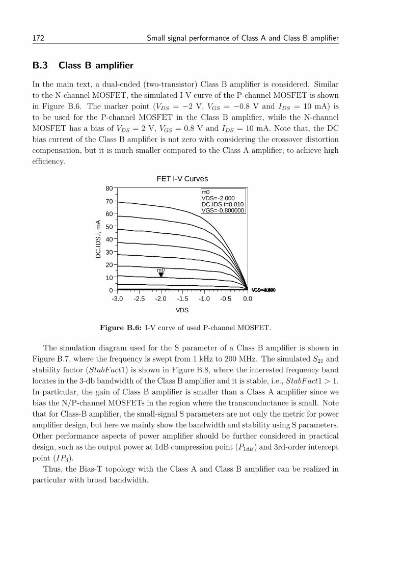
172 Small signal performance of Class A and Class B amplifier
B.3 Class B amplifier
In the main text, a dual-ended (two-transistor) Class B amplifier is considered. Similarto the N-channel MOSFET, the simulated I-V curve of the P-channel MOSFET is shownin Figure B.6. The marker point (VDS = −2 V, VGS = −0.8 V and IDS = 10 mA) isto be used for the P-channel MOSFET in the Class B amplifier, while the N-channelMOSFET has a bias of VDS = 2 V, VGS = 0.8 V and IDS = 10 mA. Note that, the DCbias current of the Class B amplifier is not zero with considering the crossover distortioncompensation, but it is much smaller compared to the Class A amplifier, to achieve highefficiency.
-2.5 -2.0 -1.5 -1.0 -0.5-3.0 0.0
10
20
30
40
50
60
70
0
80
VGS=-2.000VGS=-1.800VGS=-1.600VGS=-1.400VGS=-1.200VGS=-1.000VGS=-0.800VGS=-0.600VGS=-0.400VGS=-0.200VGS=0.000
VDS
DC
.ID
S.i, m
A
-2.0000.017
m0
FET I-V Curves
m0VDS=DC.IDS.i=0.010VGS=-0.800000
-2.000
Figure B.6: I-V curve of used P-channel MOSFET.
The simulation diagram used for the S parameter of a Class B amplifier is shown inFigure B.7, where the frequency is swept from 1 kHz to 200 MHz. The simulated S21 andstability factor (StabFact1) is shown in Figure B.8, where the interested frequency bandlocates in the 3-db bandwidth of the Class B amplifier and it is stable, i.e., StabFact1 > 1.In particular, the gain of Class B amplifier is smaller than a Class A amplifier since webias the N/P-channel MOSFETs in the region where the transconductance is small. Notethat for Class-B amplifier, the small-signal S parameters are not only the metric for poweramplifier design, but here we mainly show the bandwidth and stability using S parameters.Other performance aspects of power amplifier should be further considered in practicaldesign, such as the output power at 1dB compression point (P1dB) and 3rd-order interceptpoint (IP3).
Thus, the Bias-T topology with the Class A and Class B amplifier can be realized inparticular with broad bandwidth.

Small signal performance of Class A and Class B amplifier 173
Figure B.7: S parameter simulation diagram for Class B amplifier.
1E
4
1E
5
1E
6
1E
7
1E
8
1E
3
2E
8
4.06600
4.06605
4.06610
4.06595
4.06615
5.0E4
1.0E5
1.5E5
2.0E5
2.5E5
0.0
3.0E5
freq, Hz
dB
(S(2
,1))
Readout
m1
Readout
m2
126.2M4.066
m3
Sta
bF
act1
Readout
m4
Class B amplifier gain and stability
m1freq=dB(S(2,1))=4.066
100.1kHzm2freq=dB(S(2,1))=4.066
1.001MHzm3freq=dB(S(2,1))=4.066
100.2MHz
m4freq=StabFact1=2.762
100.2MHz
Figure B.8: Gain and stability of Class B amplifier.

174 List of the author’s publications

List of the author’s publications
Journal articles
1. X. Deng, Shokoufeh Mardanikorani, A. M. Khalid, Bin Chen, Jean-Paul M. G. Lin-nartz, ”Mitigating LED Nonlinearity to Enhance Visible Light Communications,”major revision, IEEE Transactions on Communications 2018. (SCI, IF: 4.06.)
2. X. Deng, K. Arulandu and J. P. M. G. Linnartz, ”Modelling for Transmitter PowerPerformance in High-speed Visible Light Communication Systems,” under review,IEEE Transactions on Vehicular Technology, 2018. (SCI, IF: 4.07.)
3. X. Deng, Yan Wu, Xi Long, A. M. Khalid and J. P. M. G. Linnartz, ”LED PowerConsumption in Joint Illumination and Communication System,” Opt. Express,vol. 25, no. 16, pp. 18 990–19 003, Aug 2017. (SCI, IF: 3.3.)
4. X. Deng, K. Arulandu, Y. Wu, G. Zhou and J. P. M. G. Linnartz, ”Perfor-mance Analysis for Joint Illumination and Visible Light Communication using BuckDriver,” IEEE Transactions on Communications, vol. PP, no. 99, pp. 1–1, 2018.(SCI, IF: 4.06.)
5. X. Deng, J. P. M. G. Linnartz, K. Arulandu, G. Zhou and Y. Wu, ”Reading Analy-sis for Barcode Scanner with Interference from LED-based Lighting,” in submission,IEEE Transactions on Industrial Electronics 2018. (SCI, IF: 7.17.)
Conference articles and abstracts
1. X. Deng, Y. Wu, K. Arulandu, G. Zhou and J. P. M. G. Linnartz, ”Performancecomparison for illumination and visible light communication system using buckconverters,” 2014 IEEE Globecom, Austin, TX, 2014, pp. 547-552.
175

176 List of the author’s publications
2. X. Deng, J. P. M. G. Linnartz, K. Arulandu, G. Zhou and Y. Wu, ”Effect ofbuck driver ripple on BER performance in visible light communication using LED,”2015 IEEE International Conference on Communication (ICC), London, 2015, pp.1368-1373.
3. X. Deng, P. Zijlstra, Jing Zhang, Y. Wu, G. Zhou and J. P. M. G. Linnartz,”Performance of barcode scanner using peak detection with interference from LEDlamps,” Communications and Vehicular Technology in the Benelux (SCVT), 2015IEEE Symposium on, Luxembourg City, 2015, pp. 1-6.
4. X. Deng and J. P. M. G. Linnartz, ”Model of extra power in the transmitter forhigh-speed visible light communication,” Communications and Vehicular Technol-ogy in the Benelux (SCVT), 2016 IEEE Symposium on, Mons, Belgium, 2016, pp.1-6.
Philips technical note
1. J.P.M.G. Linnartz, X. Deng, and Stepahn Nijssen, ”Impact of LED Temporal LightArtefacts on Bar Code Scanners,” Technical Note PR-TN 2016/00117, PHILIPS,2016.
Papers outside the scope of this thesis
1. X. Zou, Z. Cao, F. Zou, B. Lu, X. Yan, G. Yu, X. Deng, B. Luo, L. Yan, W. Pan,J. Yao and A. M. J. Koonen, ”Versatile integrated microwave photonic frontend andits applications in daily life,” under review, Nature Communications, 2018. (SCI,IF: 12.1.)
2. Z. Cao, X. Zhao, Y. Jiao, X. Deng, N. Tessema, O. Raz, and A. M. J. Koonen,”A Broadband Beam-Steered Fiber Mm-Wave Link with High Energy-Spectral-Spatial Efficiency for 5G Coverage,” IEEE / OSA Optical Fiber CommunicationsConference (OFC2017), California, 2017.
3. X. Zhang, Y. Tian, X. Deng, X. Lu, Z. Cao and A. M. J. Koonen, ”Inter-SubcarrierPhase Scrambling for PAPR Reduction in IM-DD OFDM System,” IEEE / OSA/SPIE Asia Communications and Photonics Conference (ACPC2017), Guangzhou,2017.
4. Z. Cao, X. Zhang, L. Shen, X. Deng, X. Yin and A. M. J. Koonen, ”MillimeterWave Beam Steered Fiber Wireless Systems for 5G Indoor Coverage: IntegratedCircuits and Systems,” IEEE / OSA/ SPIE Asia Communications and PhotonicsConference (ACPC2017), Guangzhou, 2017.

Acknowledgements
Four years ago I made a decision to pursue this PhD at TU Eindhoven (TechnischeUniversiteit Eindhoven, the Netherlands). Although every choice in life means a differentpath of life, I believe the choice I made was the best. During this four-year journey, thereare so many wonderful people surrounding me and supporting me. Herewith, I would liketo express my greatest appreciation to all of them who shared with this journey.
Foremost I am deeply grateful to my first supervisor, prof. Jean-Paul M.G. Linnartz,who initiated the framework and ideas of my PhD work. His wealth of knowledge, aca-demic excellence, enthusiasm for electronics, great ideas and patient guidance alwaysbenefit and inspire me. The fruitful discussions with him were the major momentum forthe continuous progress of my research. I have learnt a lot from him, e.g., the mathematicstyle of research, formulating skills and reasoning of ideas, and he becomes my admirablemodel of scientific expert. Besides the academic supervision, especial thanks go to himfor providing me an additional fund to finalize this thesis after my official scholarship.
I gratefully acknowledge my second supervisor, prof. Guofu Zhou, for having givenme the opportunity to pursue this PhD at TU Eindhoven. I still remember the seminarwhere we first met and I was immediately amazed by his academic achievements andpersonal charisma. My dedicated thanks go to him for the interview after that seminar,which was the key point that changed the orbit of my life. During the past four years,a special word of appreciation for his consideration, encouragements, support and helpboth for my academic research and career.
I would like to express my deep gratitude to my daily supervisor, dr. Yan Wu, for hispatience, guidance and support in my research, in particular during the first two yearsof my PhD. His considerable help in times of difficulty made me quickly adapt to thePhD work and life in Netherlands. Besides, special thanks go to him for sharing thememorable moments during the office hour, coffee break, lunch and spare time. My deepappreciation goes to dr.ir. Tjalling Tjalkens, for his amiableness and generous help. Heopened up a new door for me to understand the math underneath the communicationsystem, in particular, from the information theory perspective. The fruitful discussionswith him on mathematical problems inspired me a lot.
177

178 Acknowledgements
Enormous thanks go to Kumar Arulandu, Patrick Zijlstra and A. M. Khalid in PhilipsResearch, who worked closely with me and provided inspiring comments and contributionsfor my manuscripts and for the work in this thesis. My gratitude is also due to formerteam member Jin Zhang, who was the first master student I guided in TU Eindhoven,for being involved in my project.
Dedicated thanks to Xi Long, Lin Xu and Bin Chen, who spent time to review mymanuscripts and provide critical comments, particularly, on the scientific writing. Specialthanks to Zizheng Cao, who provided me opportunities to touch many research fieldsoutside my PhD work and our discussion is far beyond the research fields, which is veryinspiring and fascinating.
Many thanks to previous and current colleges in Intelligent Lighting group, Agis Tsi-atmas, Marina Nano, Amir, Paula, Xin Wang, Charikleia Papatsimpa, Anton Alexeev,Jochem Bonarius, Shokoufeh Mardanikorani and Mahmoud Talebi, with whom I spentthe weekly meeting and I have learnt a lot from them, although our specific researchtopics are sometimes different. Many thanks go to my officemates in potential and fluxbuilding, Wim, Bert, Marco, Thijs, Ivan, Eric, Anouk and Ismail. They created so cozyatmosphere for research and it was a grateful and pleasure time together with them.
Thanks go to the SPS group leader, Jan Bergman, for his kindness and support duringthe past years. Thanks also go to SPS and EE department secretaries for their adminis-trative assistance and many other documentary issues such as providing instructions andICT supports at the beginning of my PhD, applying business trips and reimbursement,and making support letters for my family visit to the Netherlands.
I would like to acknowledge the committee of this thesis, prof. Steve Hranilovic (Mc-Master University), prof. Liesbet Van der Perre (KU Leuven), prof. Sonia Heemstrade Groot, and the chairman prof. Jan Blom, for being part of my doctorate committeeand for the insightful comments of the thesis. Thank the anonymous reviewers for theirvaluable comments and suggestions that have greatly improved my Journal manuscripts.
During my life in the Netherlands, I have to admit that I never became homesickthanks to my Chinese friends: L. Wang, S. Sun, K. Yang, P. Zhang, Y. Wang, Y. Lei, Y.Sun, C. Li, X. Bao, H. Yang, R. Su, L. Chen, H. Zheng, X. Zhang, F. Yan, X. Xue, X.Zhao, X. Lu, Q. Liu, C. Li, L. Huang, B. Pan, M. Zhao, Y. Tian, Q. Wang, W. Miao, S.Wang, W. Yao, H. Gao, Z. Chen, B. Wang, Y. Li, Y. Li, S. Zhang, P. Sun, T. Tan, J.Zhang, H. Wang, C. Liu, S. Wang, S. Ma, S. Lu, T. Ru, H. Wang, Y. Wang, C. Zhang,J. Liu, B. Li, P. Sun, C. Wang, M. Zhang, F. Yang, G. Li, B. Han, X. Lv, W. Jiang, J.Xia, L. Chen and numerous others. Special thanks for Y. Zhang, Q. Zhang, Y. Chen andY. Zhao, who spent time with my wife and provided meticulous care for my son.
At last, this thesis is dedicated to my family. I am deeply grateful to your warminglove, unconditional support and upbringing encouragement. My inexplicable gratitudegoes to my parents, who always stand behind me in my life. I am thoroughly indebted tomy beloved wife, who continuously supports me and brings me our lovely son, William.Words are insufficient to describe my appreciation for you all being part of my life.

About the author
Xiong Deng was born on September 5, 1986 in Sichuan,China. He received his B.E. degree in electronics and in-formation engineering from Shenyang Aerospace University(SAU), China in 2009, and M.E. degrees in communicationand information engineering from University of ElectronicScience and Technology of China (UESTC), China in 2013.From 2009 to 2010, he worked with the Institute of Avi-ation Equipment, Aviation Industry Corporation of China(AVIC), on the communication system with 1553B/CANprotocol. During the period between June and Septemberin 2013, he was a researcher at Terahertz Science and Tech-nology Research Center, China Academy of Engineering Physics (CAEP), and workedon the integrated terahertz communication and imaging system. From October 2013 toSeptember 2017, he was a Ph.D candidate in the Signal Processing Systems (SPS) groupat the Eindhoven University of Technology (TU/e), the Netherlands, granted by ChinaScholarship Council (CSC). During the period of PhD, he was also a guest researcher ingroup of Internet of Things (IoT) systems, Philips Research Eindhoven, the Netherlands,on the Visible Light Communications (VLC) and Light Fidelity (LiFi). His research in-terests include the system modelling, digital signal processing and circuits for millimeterwave, radio over fibre and optical wireless communications.
179


![1 Downlink Interference Alignment - arXiv · 1 Downlink Interference Alignment Changho Suh, Minnie Ho ... 3GPP-LTE [2], require at least a doubling in cell-edge throughput over previous](https://img.dokumen.tips/doc/110x75/5adb104b7f8b9a6d318d984f/1-downlink-interference-alignment-arxiv-downlink-interference-alignment-changho.jpg)


![Cooperative Interference Neutralization in Multi-hop ...tralization, interference cancellation, throughput optimization I. ... and orthogonalize-and-forward (see, e.g., [15], [16])](https://img.dokumen.tips/doc/110x75/5ecace6b261e3667c0215f3f/cooperative-interference-neutralization-in-multi-hop-tralization-interference.jpg)