Embed Size (px)
Citation preview
Three-Terminal III-V/Si Tandem Solar Cells Enabled by a Transparent Conductive Adhesive
Journal: Sustainable Energy & Fuels
Manuscript ID SE-ART-10-2019-000893
Article Type: Paper
Date Submitted by the Author: 08-Aug-2019
Complete List of Authors: Schnabel, Manuel; National Renewable Energy Laboratory, Schulte-Huxel, Henning; Institut fur Solarenergieforschung GmbH, PhotovoltaicsRienäcker, Michael; Institut fur Solarenergieforschung GmbH, PhotovoltaicsWarren, Emily; National Renewable Energy LaboratoryNdione, Paul; National Renewable Energy Laboratory, Nemeth, William; National Renewable Energy LaboratoryKlein, Talysa; National Renewable Energy Laboratoryvan Hest, Maikel; National Renewable Energy Laboratory, Geisz, John; National Renewable Energy Laboratory, Peibst, Robby; Institut fur Solarenergieforschung GmbHStradins, Paul; National Renewable Energy Laboratory, National Center for PhotovoltaicsTamboli, Adele; National Renewable Energy Lab, ; Colorado School of Mines, Physics
Sustainable Energy & Fuels
Journal Name
ARTICLE
This journal is © The Royal Society of Chemistry 20xx J. Name., 2013, 00, 1-3 | 1
Please do not adjust margins
Please do not adjust margins
Received 00th January 20xx,Accepted 00th January 20xx
DOI: 10.1039/x0xx00000x
www.rsc.org/
Three-Terminal III-V/Si Tandem Solar Cells Enabled by a Transparent Conductive AdhesiveManuel Schnabel,*a Henning Schulte-Huxel,a,b Michael Rienäcker,b Emily L. Warren,a Paul F. Ndione,a Bill Nemeth,a Talysa R. Klein,a Maikel F.A.M. van Hest,a John F. Geisz,a Robby Peibst,b Paul Stradins,a Adele C. Tambolia
Tandem or multijunction solar cells are able to convert sunlight to electricity with greater efficiency than single junction solar cells by splitting the solar spectrum across sub-cells with different bandgaps. With the efficiencies of many common single-junction solar cell materials levelling off near their theoretical efficiency limits, there is renewed interest in applying this approach. However, there is ongoing debate as to the best approach for interconnecting sub-cells in series, or whether it is preferable to operate them independently. In this paper, we provide the first experimental demonstration of a tandem cell architecture with three terminals: one on top of the tandem cell, and two beneath it, in interdigitated back contact configuration. The two cells are interconnected with a transparent conductive adhesive, which is compatible with rough surfaces and exhibits negligible series resistance. Combining GaInP and Si sub-cells in this manner allows us to achieve a GaInP/Si tandem cell with a two-terminal efficiency of 26.4 ± 1.0 %. We then show that utilizing all three terminals results in an efficiency boost of 0.9 ± 0.2 %, to an efficiency of 27.3 ± 1.0 %, and discuss the operation of the cell and its two interacting circuits.
1 IntroductionSilicon solar cells dominate the photovoltaics (PV) market,2 but laboratory-level efficiencies have converged close to the theoretical efficiency limit.3, 4 This has stimulated strong interest in Si-based hybrid tandem cells,5-7 where one or more wider bandgap solar cells are combined with a silicon bottom cell in order to overcome the single-junction detailed balance efficiency limit.8, 9 Silicon has a bandgap that is close to ideal for the bottom cell in a tandem cell,10 and is a mature photovoltaic material that can facilitate the transfer of new device architectures to mass production. Tandem solar cells are of great practical interest because a large part of the cost of a PV system consists of area-dependent balance-of-system costs, and tandem cells promise to deliver more energy per unit area.11, 12
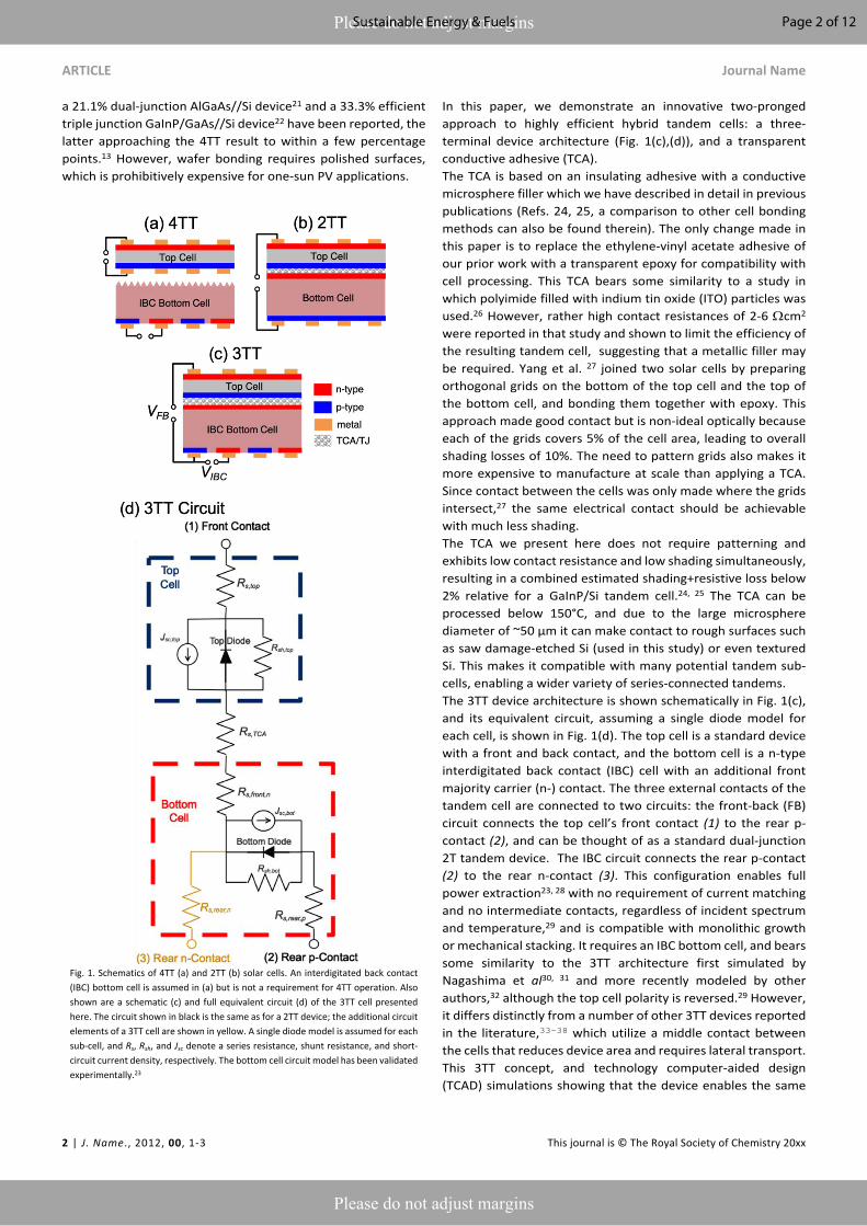
The highest tandem cell efficiencies have been achieved with four-terminal tandem (4TT) devices in which two sub-cells are operated independently (Fig. 1(a)). The most common alternative is a two-terminal tandem (2TT) approach where sub-cells are connected in series using a tunnel junction (TJ) or transparent conducting adhesive (TCA), (Fig. 1(b)). In this paper, we demonstrate experimentally a novel three-terminal tandem (3TT) architecture as a promising third option (Fig. 1(c),(d)).
The 4TT approach has enabled Si-based tandem cells with top cells made out of III-V semiconductors that exhibit efficiencies of up to 32.8% for two junctions and 35.9% for three junctions.13 Si can also be paired with wide-bandgap perovskites; this approach has yielded 26.4%.14 The advantage of the 4TT approach is that all generated power can be extracted irrespective of the sub-cell bandgaps or the incident spectrum. However, it does require transparent, laterally conductive layers at electrodes located between the sub-cells, and as cell areas are scaled up, these layers can lead to significant optical and resistive losses and drive up manufacturing costs. 2TT cells solve this problem by connecting sub-cells in series, thus doing away with intermediate electrodes and providing a drop-in replacement for single-junction solar cells. However, the sub-cells now have to be current-matched to work efficiently, which means top cell materials to be paired with Si must have a bandgap close to 1.7 eV.15 Furthermore, the cells must either be grown on top of one another or joined with a conductive bond.Perovskite solar cells have been successfully processed on Si, and 2TT efficiencies of 25.0-25.4% have been obtained in multiple studies.16-18 A company focussing exclusively on perovskite/Si tandem cells has recently reported 28%.19 Conversely, the direct growth of III-V solar cells on silicon has only had limited success due to the high crystalline quality that must be maintained in both materials, and efficiencies under the standard terrestrial solar spectrum AM1.5G have only recently reached 20.1% for a dual-junction cell and 22.3% for a triple-junction device.3 The conductive bonding of III-V materials to Si has been more successful: using wafer bonding,20
a.National Renewable Energy Laboratory, Golden CO 80401, USAb. Institute for Solar Energy Research Hamelin, D-31860 Emmerthal, Germany
Page 1 of 12 Sustainable Energy & Fuels
ARTICLE Journal Name
2 | J. Name., 2012, 00, 1-3 This journal is © The Royal Society of Chemistry 20xx
Please do not adjust margins
Please do not adjust margins
a 21.1% dual-junction AlGaAs//Si device21 and a 33.3% efficient triple junction GaInP/GaAs//Si device22 have been reported, the latter approaching the 4TT result to within a few percentage points.13 However, wafer bonding requires polished surfaces, which is prohibitively expensive for one-sun PV applications.
Fig. 1. Schematics of 4TT (a) and 2TT (b) solar cells. An interdigitated back contact (IBC) bottom cell is assumed in (a) but is not a requirement for 4TT operation. Also shown are a schematic (c) and full equivalent circuit (d) of the 3TT cell presented here. The circuit shown in black is the same as for a 2TT device; the additional circuit elements of a 3TT cell are shown in yellow. A single diode model is assumed for each sub-cell, and Rs, Rsh, and Jsc denote a series resistance, shunt resistance, and short-circuit current density, respectively. The bottom cell circuit model has been validated experimentally.23
In this paper, we demonstrate an innovative two-pronged approach to highly efficient hybrid tandem cells: a three-terminal device architecture (Fig. 1(c),(d)), and a transparent conductive adhesive (TCA). The TCA is based on an insulating adhesive with a conductive microsphere filler which we have described in detail in previous publications (Refs. 24, 25, a comparison to other cell bonding methods can also be found therein). The only change made in this paper is to replace the ethylene-vinyl acetate adhesive of our prior work with a transparent epoxy for compatibility with cell processing. This TCA bears some similarity to a study in which polyimide filled with indium tin oxide (ITO) particles was used.26 However, rather high contact resistances of 2-6 cm2 were reported in that study and shown to limit the efficiency of the resulting tandem cell, suggesting that a metallic filler may be required. Yang et al. 27 joined two solar cells by preparing orthogonal grids on the bottom of the top cell and the top of the bottom cell, and bonding them together with epoxy. This approach made good contact but is non-ideal optically because each of the grids covers 5% of the cell area, leading to overall shading losses of 10%. The need to pattern grids also makes it more expensive to manufacture at scale than applying a TCA. Since contact between the cells was only made where the grids intersect,27 the same electrical contact should be achievable with much less shading.The TCA we present here does not require patterning and exhibits low contact resistance and low shading simultaneously, resulting in a combined estimated shading+resistive loss below 2% relative for a GaInP/Si tandem cell.24, 25 The TCA can be processed below 150°C, and due to the large microsphere diameter of ~50 µm it can make contact to rough surfaces such as saw damage-etched Si (used in this study) or even textured Si. This makes it compatible with many potential tandem sub-cells, enabling a wider variety of series-connected tandems. The 3TT device architecture is shown schematically in Fig. 1(c), and its equivalent circuit, assuming a single diode model for each cell, is shown in Fig. 1(d). The top cell is a standard device with a front and back contact, and the bottom cell is a n-type interdigitated back contact (IBC) cell with an additional front majority carrier (n-) contact. The three external contacts of the tandem cell are connected to two circuits: the front-back (FB) circuit connects the top cell’s front contact (1) to the rear p-contact (2), and can be thought of as a standard dual-junction 2T tandem device. The IBC circuit connects the rear p-contact (2) to the rear n-contact (3). This configuration enables full power extraction23, 28 with no requirement of current matching and no intermediate contacts, regardless of incident spectrum and temperature,29 and is compatible with monolithic growth or mechanical stacking. It requires an IBC bottom cell, and bears some similarity to the 3TT architecture first simulated by Nagashima et al30, 31 and more recently modeled by other authors,32 although the top cell polarity is reversed.29 However, it differs distinctly from a number of other 3TT devices reported in the literature,33-38 which utilize a middle contact between the cells that reduces device area and requires lateral transport. This 3TT concept, and technology computer-aided design (TCAD) simulations showing that the device enables the same
Page 2 of 12Sustainable Energy & Fuels
Journal Name ARTICLE
This journal is © The Royal Society of Chemistry 20xx J. Name., 2013, 00, 1-3 | 3
Please do not adjust margins
Please do not adjust margins
performance as 4TT cells, have been presented previously;23, 29 here, we experimentally demonstrate the first 3TT device with this architecture. We use a GaInP top cell and a 3T Si bottom cell23 conductively bonded together with a TCA, and we first show how this interconnection was optimized, which allowed us to achieve a 2TT efficiency of 26.4%. This exceeds the record efficiency of individual GaInP cells and approaches that of individual Si solar cells (21.4% and 26.7%, respectively)3 and is among the highest efficiencies reported for a series-connected dual-junction tandem cell with silicon.3, 16, 17, 19, 39 We then demonstrate that the third terminal allows 0.9% absolute more power to be extracted, boosting the efficiency from 26.4% to 27.3%, and report on the operating mechanism of the 3TT device.
2 ExperimentalThe 3T Si bottom cell, and the III-V layer stack of the GaInP top cell, are first prepared separately. The latter is grown inverted on a sacrificial GaAs substrate. Then, the two are bonded together using the TCA, the GaAs substrate is removed, and GaInP cell processing is completed on top of the Si cell. A schematic of the resulting 3TT device is shown in Fig. 2(a). A 4TT GaInP/Si reference tandem cell (with the structure shown schematically in Fig. 1(a)) was also prepared, following the process chain in Refs. 1, 13 but utilizing an IBC Si cell. The 3TT process chain is detailed in the following.
Sub-Cell Preparation
The GaInP cell stack40 was grown inverted on GaAs substrates with a 2° miscut towards <111>B by metalorganic chemical vapor deposition (MOCVD), using the reactor, precursors, and process window described previously.41 The rear hetero-junction design40 was used in this stack for high performance. The layer stack is identical to that used for the GaInP top cell in Refs. 1, 13 (see also Fig. 2(a)). One sample was processed exactly as described in Ref. 1 to prepare a 4TT reference device.The 3T Si bottom cells with doped poly-Si on passivating oxide (POLO) contacts were prepared using 160 μm thick n-type Cz-Si wafers. IBC cell processing largely follows the process described in Ref. 42, except that cell dimensions were adapted to match the III-V top cell, and that the textured front side with dielectric passivation layers was replaced by a planar front side with a n-type POLO contact (also referred to as a front-surface-field (FSF)).23 This well-passivated front contact forms the front terminal of the 3T Si cell. A planar front side is selected for the Si cell for simplicity for this proof-of-concept, but subsequent processing is compatible with textured Si.24 The 3T Si cell also has two interdigitated rear contacts: a rear n-contact (also referred to as a back-surface-field (BSF)), and a rear p-contact (also referred to as an emitter). Two layers of Fujifilm SC-900 photoresist were processed onto the rear side of the Si cell to protect it during further processing and are removed with toluene at the end of the process chain. A cell with a conventional front side42 but the same dimensions was also processed in order to prepare a 4TT reference device.
Bonding III-V to Si using a Transparent Conducting Adhesive
In order to improve the electrical contact between the TCA and either cell, the bottom of the GaInP top cell, and the n-poly-Si at the top of the Si bottom cell, are both coated with ~95 nm indium tin oxide (ITO) sputtered at a substrate temperature of 200°C and a power of 0.3 mW cm-2 (see Fig. 2(a)), in a MVSystems tool using a 90% SnO2-10% In2O3 target (Plasmaterials) and a 13.56 MHz radio frequency (RF) source. The recipe was the result of an optimization process described in the Results section and Supplementary Information.
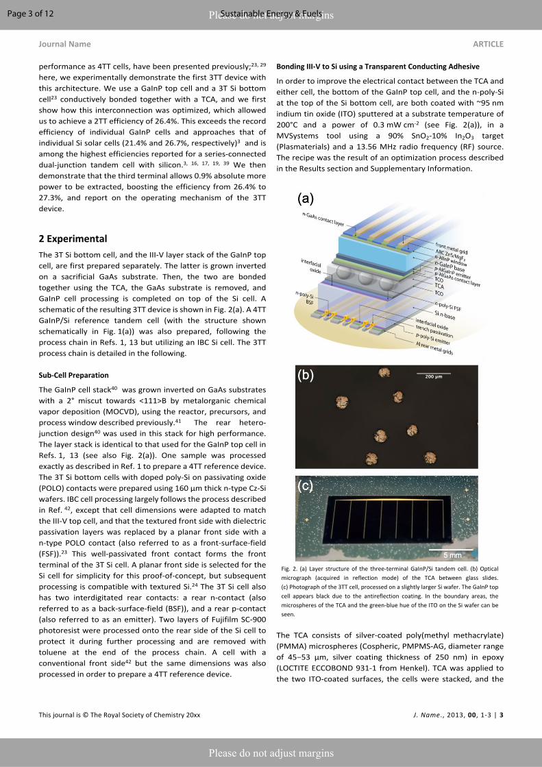
Fig. 2. (a) Layer structure of the three-terminal GaInP/Si tandem cell. (b) Optical micrograph (acquired in reflection mode) of the TCA between glass slides. (c) Photograph of the 3TT cell, processed on a slightly larger Si wafer. The GaInP top cell appears black due to the antireflection coating. In the boundary areas, the microspheres of the TCA and the green-blue hue of the ITO on the Si wafer can be seen.
The TCA consists of silver-coated poly(methyl methacrylate) (PMMA) microspheres (Cospheric, PMPMS-AG, diameter range of 45−53 μm, silver coating thickness of 250 nm) in epoxy (LOCTITE ECCOBOND 931-1 from Henkel). TCA was applied to the two ITO-coated surfaces, the cells were stacked, and the
Page 3 of 12 Sustainable Energy & Fuels
ARTICLE Journal Name
4 | J. Name., 2012, 00, 1-3 This journal is © The Royal Society of Chemistry 20xx
Please do not adjust margins
Please do not adjust margins
GaInP/TCA/Si stack was then pressed at a nominal pressure of 0.5 bar and 120°C for 20 min. Figure 2(b) shows an optical micrograph of a comparable TCA layer pressed between glass slides; the gaps between the spheres are filled with transparent epoxy. The area coverage of microspheres in the final device, determined by representative microscope images sampled across the active cell area, was 3.1% ± 0.4%.
Tandem Cell Processing
As the GaInP cell was grown inverted on GaAs, processing of the GaInP/TCA/Si stack begins by etching off the GaAs substrate. A photolithographically defined Ni/Au grid was plated onto the front of the GaInP top cell, and the cell area was isolated by a photolithographically defined mesa etch (a smaller area is subsequently defined by a shadow mask during characterization). The GaAs contact layer was etched between the grid fingers, and a MgF2/ZnS double-layer antireflection coating (ARC) was evaporated onto the front of the finished 3T tandem cell to give the device structure shown in Fig. 2(a). A photograph of the finished cell is shown in Fig. 2(c). The electroplated grid covers 2.6% of the cell area, so total shading losses to the bottom cell arising from the grid and the TCA are 5.7%, assuming no overlap of the TCA microspheres and the grid.
Characterization
A custom-built instrument was used to measure the reflectance of tandem cells with different ARCs (Fig. 3), as well as external quantum efficiency (EQE, shown in Fig. 4(c)) of the 3TT device and the 4TT reference cell. The EQE curves were used to set spectral-mismatch-corrected one-sun AM1.5G conditions43 during the subsequent solar cell measurement. Solar cells were measured under AM1.5G illumination by measuring the current density as a function of voltage, yielding illuminated current voltage (light IV, LIV) curves. The EQEs of the GaInP and Si sub-cells of the 3TT device were measured using contacts 1 and 2 (Fig. 1(d)), and light-biasing the sub-cell that was not under test.44 The Si sub-cell EQE was corrected for luminescent coupling.45 The EQEs of the sub-cells of the 4TT reference device were measured using the respective sub-cell contacts. Due to the absence of bias light, no luminescent coupling correction was found to be necessary. Short-circuit current densities Jsc derived from measured EQE curves agreed with those from LIV measurements to within experimental error; more details are provided in Table S2 in the Supplementary Information.The LIV measurements were taken on a class A adjustable solar simulator, with calibrated reference cells43 used to set the intensity. LEDs were used in addition to the simulator’s Xenon lamp in order to achieve AM1.5G conditions in both sub-cells simultaneously. A custom-built jig was used to enable simultaneous probing of all three terminals. The two-terminal tandem cell LIV curve (2TT LIV) of the 3TT cell was acquired using contacts 1 and 2 (Fig. 1(d), inset Fig. 4(a)), and the LIV of the GaInP and Si sub-cells of the 3TT cell were measured by probing contacts 1 and 3, and 2 and 3, respectively
(Fig. 1(d), insets in Fig. 4(b)), with the remaining terminal held open. It should be noted that the GaInP and Si IBC LIV curves thus measured for the 3TT device are not a perfect measurement of the corresponding sub-cell because the GaInP LIV is measured with an additional series resistance Rs=Rs,TCA+Rs,front,n+Rs,rear,n, and the Si IBC LIV curve is measured with the GaInP sub-cell at open circuit which induces excess luminescent coupling. Therefore no absolute efficiencies are reported for these measurements in Table 2. However, these effects are small enough that the sub-cell LIV curves still constitute a useful diagnostic tool. For the 4TT device, GaInP and Si IBC LIV curves were acquired with the respective sub-cell contacts, and the 2TT LIV is acquired by externally connecting the GaInP and Si sub-cells in series (see Fig. (a),(b) insets). When referring to LIV curves, we adopt a nomenclature where 2TT, GaInP, and Si IBC denote the measurement circuit, and 3TT and 4TT denote the physical device being measured.As the two circuits of a 3TT cell during 3T operation (Fig. 1(c),(d)) both contain the Si diode, they interact, which means that for a correct measurement of the total 3TT efficiency the two circuits must be measured simultaneously. A pair of voltages VFB, VIBC is applied using two sourcemeters, and the resulting current densities JFB, JIBC in the respective circuits are measured. This is repeated for many sets of VFB, VIBC to build up current density maps in VFB-VIBC space, which are most conveniently visualized as contour plots (Fig. 5(b),(c)). These current densities are then multiplied by the corresponding voltage to obtain power density maps (PFB, PIBC), which are added to obtain a map of the total 3TT power density Ptot= PFB+PIBC (Fig. 5(a)).The active cell area of the 3TT cell was defined by a shadow mask and contains the front grid and busbar but not the IBC busbars of the Si cell and is 0.567 ± 0.001 cm2. Absolute errors in LIV measurements (random and systematic) were determined by conferring with NREL’s certification laboratory to determine their errors and increasing them to account for any additional errors we expect from our setup. For efficiency differences across LIV measurements in a given measurement session, systematic errors cancel out, and only a random error extracted from the range of values obtained upon repeated measurement is applied. More details on error analysis can be found in the Supplementary Information.
3 Results and DiscussionMaterials Optimization
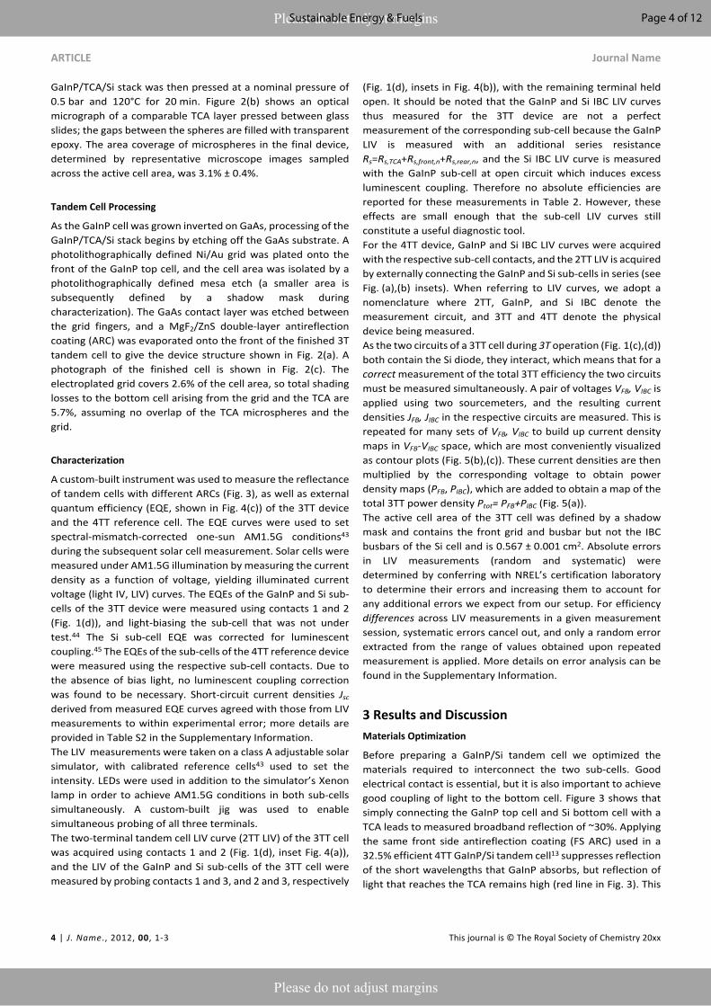
Before preparing a GaInP/Si tandem cell we optimized the materials required to interconnect the two sub-cells. Good electrical contact is essential, but it is also important to achieve good coupling of light to the bottom cell. Figure 3 shows that simply connecting the GaInP top cell and Si bottom cell with a TCA leads to measured broadband reflection of ~30%. Applying the same front side antireflection coating (FS ARC) used in a 32.5% efficient 4TT GaInP/Si tandem cell13 suppresses reflection of the short wavelengths that GaInP absorbs, but reflection of light that reaches the TCA remains high (red line in Fig. 3). This
Page 4 of 12Sustainable Energy & Fuels
Journal Name ARTICLE
This journal is © The Royal Society of Chemistry 20xx J. Name., 2013, 00, 1-3 | 5
Please do not adjust margins
Please do not adjust margins
is not unexpected since the TCA has a much lower refractive index (n1.6) than GaInP and Si, and indicates that refractive index grading from GaInP to TCA, and TCA to Si, is required to reduce reflection. In a 3TT device the index grading must be achieved with conductive layers such as transparent conductive oxides (TCOs).46 In this study, indium tin oxide (ITO) is used.
Fig. 3. Measured reflectance of GaInP/Si tandem cells interconnected with a TCA, for a cell with no ARC (black), front side (FS) ARC only (red), and FS ARC + intermediate ITO layers (blue).
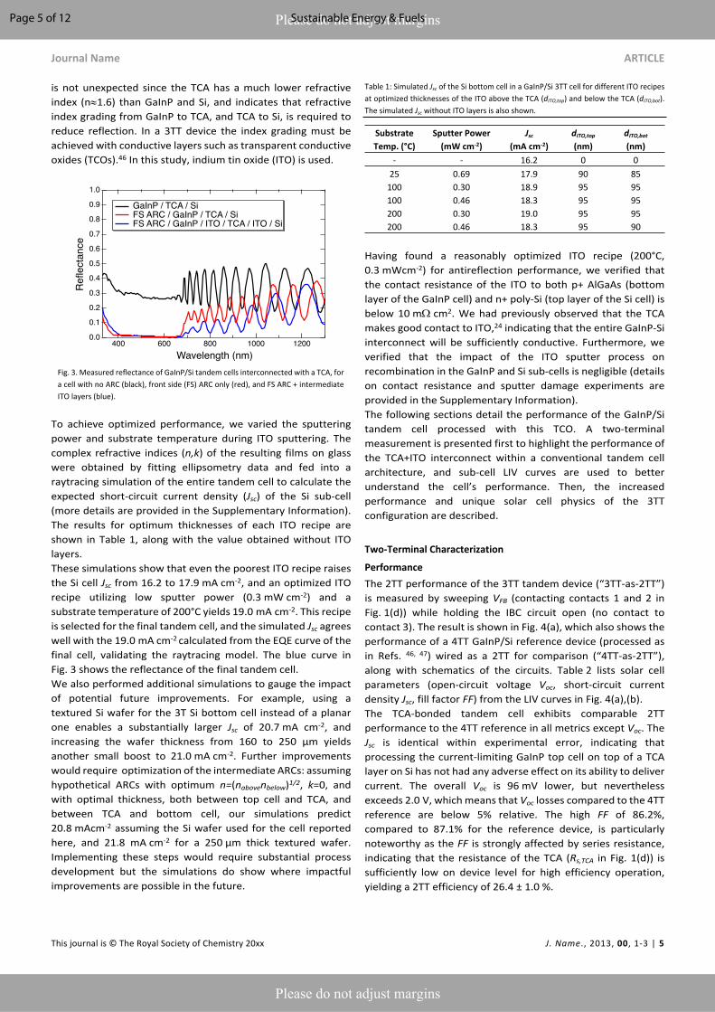
To achieve optimized performance, we varied the sputtering power and substrate temperature during ITO sputtering. The complex refractive indices (n,k) of the resulting films on glass were obtained by fitting ellipsometry data and fed into a raytracing simulation of the entire tandem cell to calculate the expected short-circuit current density (Jsc) of the Si sub-cell (more details are provided in the Supplementary Information). The results for optimum thicknesses of each ITO recipe are shown in Table 1, along with the value obtained without ITO layers. These simulations show that even the poorest ITO recipe raises the Si cell Jsc from 16.2 to 17.9 mA cm-2, and an optimized ITO recipe utilizing low sputter power (0.3 mW cm-2) and a substrate temperature of 200°C yields 19.0 mA cm-2. This recipe is selected for the final tandem cell, and the simulated Jsc agrees well with the 19.0 mA cm-2 calculated from the EQE curve of the final cell, validating the raytracing model. The blue curve in Fig. 3 shows the reflectance of the final tandem cell. We also performed additional simulations to gauge the impact of potential future improvements. For example, using a textured Si wafer for the 3T Si bottom cell instead of a planar one enables a substantially larger Jsc of 20.7 mA cm-2, and increasing the wafer thickness from 160 to 250 µm yields another small boost to 21.0 mA cm-2. Further improvements would require optimization of the intermediate ARCs: assuming hypothetical ARCs with optimum n=(nabovenbelow)1/2, k=0, and with optimal thickness, both between top cell and TCA, and between TCA and bottom cell, our simulations predict 20.8 mAcm-2 assuming the Si wafer used for the cell reported here, and 21.8 mA cm-2 for a 250 µm thick textured wafer. Implementing these steps would require substantial process development but the simulations do show where impactful improvements are possible in the future.
Table 1: Simulated Jsc of the Si bottom cell in a GaInP/Si 3TT cell for different ITO recipes at optimized thicknesses of the ITO above the TCA (dITO,top) and below the TCA (dITO,bot). The simulated Jsc without ITO layers is also shown.
Substrate Temp. (°C)
Sputter Power (mW cm-2)
Jsc (mA cm-2)
dITO,top (nm)
dITO,bot (nm)
- - 16.2 0 025 0.69 17.9 90 85
100 0.30 18.9 95 95100 0.46 18.3 95 95200 0.30 19.0 95 95200 0.46 18.3 95 90
Having found a reasonably optimized ITO recipe (200°C, 0.3 mWcm-2) for antireflection performance, we verified that the contact resistance of the ITO to both p+ AlGaAs (bottom layer of the GaInP cell) and n+ poly-Si (top layer of the Si cell) is below 10 m cm2. We had previously observed that the TCA makes good contact to ITO,24 indicating that the entire GaInP-Si interconnect will be sufficiently conductive. Furthermore, we verified that the impact of the ITO sputter process on recombination in the GaInP and Si sub-cells is negligible (details on contact resistance and sputter damage experiments are provided in the Supplementary Information). The following sections detail the performance of the GaInP/Si tandem cell processed with this TCO. A two-terminal measurement is presented first to highlight the performance of the TCA+ITO interconnect within a conventional tandem cell architecture, and sub-cell LIV curves are used to better understand the cell’s performance. Then, the increased performance and unique solar cell physics of the 3TT configuration are described.
Two-Terminal Characterization
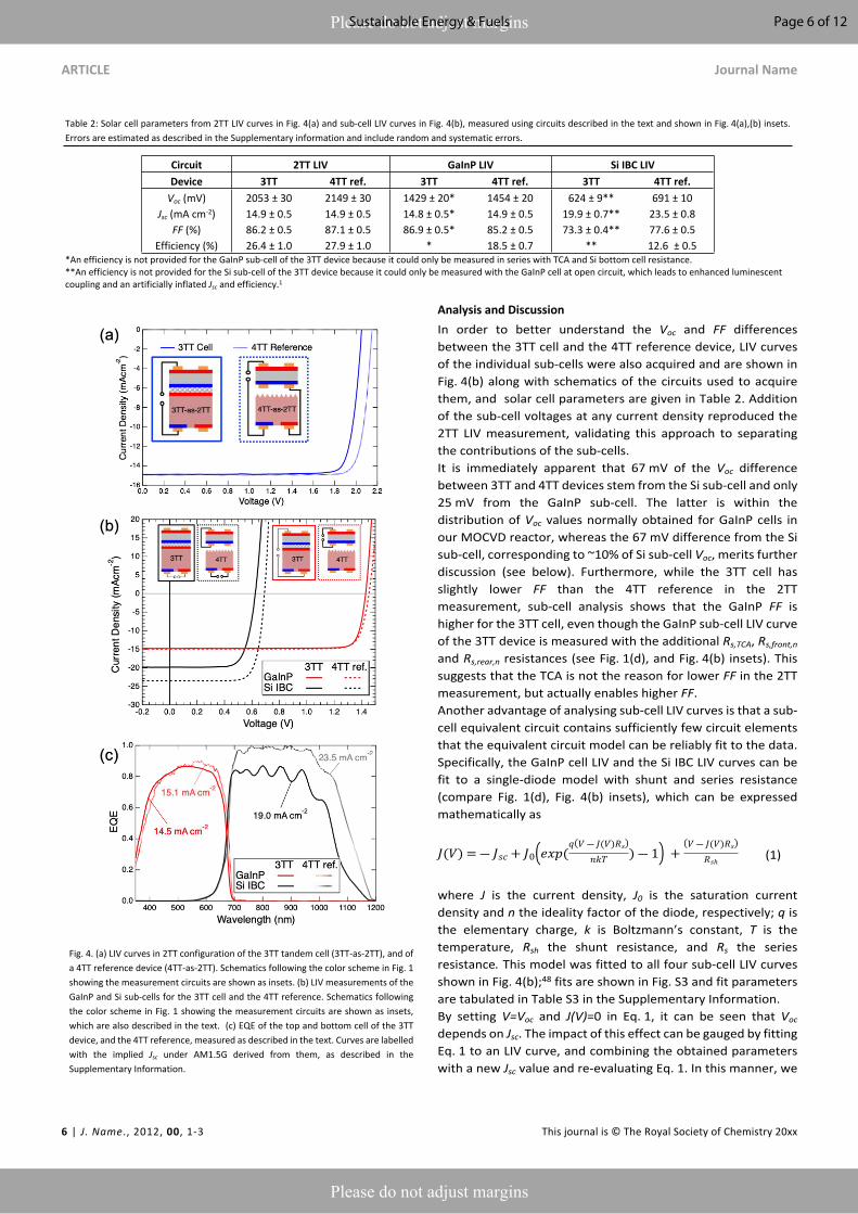
PerformanceThe 2TT performance of the 3TT tandem device (“3TT-as-2TT”) is measured by sweeping VFB (contacting contacts 1 and 2 in Fig. 1(d)) while holding the IBC circuit open (no contact to contact 3). The result is shown in Fig. 4(a), which also shows the performance of a 4TT GaInP/Si reference device (processed as in Refs. 46, 47) wired as a 2TT for comparison (“4TT-as-2TT”), along with schematics of the circuits. Table 2 lists solar cell parameters (open-circuit voltage Voc, short-circuit current density Jsc, fill factor FF) from the LIV curves in Fig. 4(a),(b). The TCA-bonded tandem cell exhibits comparable 2TT performance to the 4TT reference in all metrics except Voc. The Jsc is identical within experimental error, indicating that processing the current-limiting GaInP top cell on top of a TCA layer on Si has not had any adverse effect on its ability to deliver current. The overall Voc is 96 mV lower, but nevertheless exceeds 2.0 V, which means that Voc losses compared to the 4TT reference are below 5% relative. The high FF of 86.2%, compared to 87.1% for the reference device, is particularly noteworthy as the FF is strongly affected by series resistance, indicating that the resistance of the TCA (Rs,TCA in Fig. 1(d)) is sufficiently low on device level for high efficiency operation, yielding a 2TT efficiency of 26.4 ± 1.0 %.
Page 5 of 12 Sustainable Energy & Fuels
ARTICLE Journal Name
6 | J. Name., 2012, 00, 1-3 This journal is © The Royal Society of Chemistry 20xx
Please do not adjust margins
Please do not adjust margins
Fig. 4. (a) LIV curves in 2TT configuration of the 3TT tandem cell (3TT-as-2TT), and of a 4TT reference device (4TT-as-2TT). Schematics following the color scheme in Fig. 1 showing the measurement circuits are shown as insets. (b) LIV measurements of the GaInP and Si sub-cells for the 3TT cell and the 4TT reference. Schematics following the color scheme in Fig. 1 showing the measurement circuits are shown as insets, which are also described in the text. (c) EQE of the top and bottom cell of the 3TT device, and the 4TT reference, measured as described in the text. Curves are labelled with the implied Jsc under AM1.5G derived from them, as described in the Supplementary Information.
Analysis and DiscussionIn order to better understand the Voc and FF differences between the 3TT cell and the 4TT reference device, LIV curves of the individual sub-cells were also acquired and are shown in Fig. 4(b) along with schematics of the circuits used to acquire them, and solar cell parameters are given in Table 2. Addition of the sub-cell voltages at any current density reproduced the 2TT LIV measurement, validating this approach to separating the contributions of the sub-cells.It is immediately apparent that 67 mV of the Voc difference between 3TT and 4TT devices stem from the Si sub-cell and only 25 mV from the GaInP sub-cell. The latter is within the distribution of Voc values normally obtained for GaInP cells in our MOCVD reactor, whereas the 67 mV difference from the Si sub-cell, corresponding to ~10% of Si sub-cell Voc, merits further discussion (see below). Furthermore, while the 3TT cell has slightly lower FF than the 4TT reference in the 2TT measurement, sub-cell analysis shows that the GaInP FF is higher for the 3TT cell, even though the GaInP sub-cell LIV curve of the 3TT device is measured with the additional Rs,TCA, Rs,front,n and Rs,rear,n resistances (see Fig. 1(d), and Fig. 4(b) insets). This suggests that the TCA is not the reason for lower FF in the 2TT measurement, but actually enables higher FF.Another advantage of analysing sub-cell LIV curves is that a sub-cell equivalent circuit contains sufficiently few circuit elements that the equivalent circuit model can be reliably fit to the data. Specifically, the GaInP cell LIV and the Si IBC LIV curves can be fit to a single-diode model with shunt and series resistance (compare Fig. 1(d), Fig. 4(b) insets), which can be expressed mathematically as
(1)𝐽(𝑉) = ― 𝐽𝑠𝑐 + 𝐽0(𝑒𝑥𝑝(𝑞(𝑉 ― 𝐽(𝑉)𝑅𝑠)
𝑛𝑘𝑇 ) ― 1) +(𝑉 ― 𝐽(𝑉)𝑅𝑠)
𝑅𝑠ℎ
where J is the current density, J0 is the saturation current density and n the ideality factor of the diode, respectively; q is the elementary charge, k is Boltzmann’s constant, T is the temperature, Rsh the shunt resistance, and Rs the series resistance. This model was fitted to all four sub-cell LIV curves shown in Fig. 4(b);48 fits are shown in Fig. S3 and fit parameters are tabulated in Table S3 in the Supplementary Information. By setting V=Voc and J(V)=0 in Eq. 1, it can be seen that Voc depends on Jsc. The impact of this effect can be gauged by fitting Eq. 1 to an LIV curve, and combining the obtained parameters with a new Jsc value and re-evaluating Eq. 1. In this manner, we
Table 2: Solar cell parameters from 2TT LIV curves in Fig. 4(a) and sub-cell LIV curves in Fig. 4(b), measured using circuits described in the text and shown in Fig. 4(a),(b) insets. Errors are estimated as described in the Supplementary information and include random and systematic errors.
Circuit 2TT LIV GaInP LIV Si IBC LIVDevice 3TT 4TT ref. 3TT 4TT ref. 3TT 4TT ref.
Voc (mV) 2053 ± 30 2149 ± 30 1429 ± 20* 1454 ± 20 624 ± 9** 691 ± 10Jsc (mA cm-2) 14.9 ± 0.5 14.9 ± 0.5 14.8 ± 0.5* 14.9 ± 0.5 19.9 ± 0.7** 23.5 ± 0.8
FF (%) 86.2 ± 0.5 87.1 ± 0.5 86.9 ± 0.5* 85.2 ± 0.5 73.3 ± 0.4** 77.6 ± 0.5Efficiency (%) 26.4 ± 1.0 27.9 ± 1.0 * 18.5 ± 0.7 ** 12.6 ± 0.5
*An efficiency is not provided for the GaInP sub-cell of the 3TT device because it could only be measured in series with TCA and Si bottom cell resistance. **An efficiency is not provided for the Si sub-cell of the 3TT device because it could only be measured with the GaInP cell at open circuit, which leads to enhanced luminescent coupling and an artificially inflated Jsc and efficiency.1
Page 6 of 12Sustainable Energy & Fuels
Journal Name ARTICLE
This journal is © The Royal Society of Chemistry 20xx J. Name., 2013, 00, 1-3 | 7
Please do not adjust margins
Please do not adjust margins
find that the difference in Jsc between Si IBC sub-cells in the 3TT and 4TT devices only accounts for a 7 mV Voc difference. We also applied this approach to the LIV curve of the 3T Si sub-cell prior to tandem cell processing (not shown), and found that prior to processing it would have had the same Voc as the Si sub-cell in the 4TT device. The main cause of the Voc difference is therefore 3TT process-induced damage to the Si sub-cell, e.g. from exposure to chemicals during top cell processing and repeated thermal cycling. Fortunately, the 3TT architecture is not dependent on this precise process chain, and different implementations of it need not suffer from this effect. Fits of Eq. 1 to the sub-cell LIV curves also allow us to determine the corresponding series resistance Rs, which as Fig. 1(d) shows for the case of the 3TT device is actually the sum of several Rs terms for either sub-cell circuit. For example, for the GaInP LIV curve, measured via contacts 1 and 3 in the 3TT cell, Rs=Rs,top+Rs,TCA+Rs,front,n+Rs,rear,n, i.e. including the TCA, and we find Rs=0.6 cm2. Meanwhile, the GaInP sub-cell of the 4TT reference exhibits Rs=0.9 cm2. This means that in the 3TT device, Rs,TCA+Rs,front,n+Rs,rear,n together is lower than the resistance of the rear contact of the GaInP sub-cell in the 4TT reference (all other parts of the GaInP sub-cells being identical). Rather than contributing more series resistance, the TCA is shown to be so conductive that it lowers the series resistance of the top cell as compared to a rear grid. This advantage is expected to be even more pronounced in larger area solar cells as the purely vertical current flow across the TCA in a 3TT cell proceeds at an area-independent current density whereas the lateral current flow required at the rear of the top cell and front of the bottom cell in 4TT devices yields large lateral current densities for larger cells that are increasingly difficult to sustain without resistive losses.Conversely, for the Si IBC LIV curves we extract Rs=0.6 cm2 for the 3TT device and Rs=0.3 cm2 for the 4TT reference, correlating with Si IBC FF values of 73.3% and 77.6%, respectively (although the lower 3TT Si sub-cell Voc also contributes). It is therefore the Si diode and Rs,rear,p which are responsible for the lower 2TT FF of the 3TT device, not the n-type Si contacts, the TCA or the GaInP cell. We also extracted 2TT Rs values as follows: we took all Eq. 1 fit parameters from all sub-cell LIV curves, discarded Rs values, and set up the 2TT LIV model (black elements in Fig. 1(d)) in the circuit simulator LTSpice. Then we combined all resistors into one Rs term (for 2TT, Rs=Rs,top+Rs,TCA+Rs,front,n+Rs,rear,p), and ran the simulation for a range of Rs values to obtain a fit to the experimental 2TT LIV data. We obtained Rs=1.0 cm2 for the 3TT device, and Rs=1.1 cm2 for the 4TT reference, which are very similar to each other and to the sum of respective sub-cell Rs values. This shows that the higher Si resistance cancelled out the lower Rs of the TCA in our particular 3TT device as compared to the 4TT reference.Nevertheless, all these factors combined to give a 2TT efficiency of 26.4% for our TCA-bonded device, which among the highest efficiencies reported for a series-connected two-junction tandem cell involving silicon.3, 16, 17, 39 It should be noted that this excellent device performance stems mainly from the high Voc and FF, enabled in no small part by the TCA. The current is
severely limited by the GaInP top cell, and we now proceed to utilize the third terminal to extract the excess current of the Si bottom cell.
Three-Terminal Performance and Operation
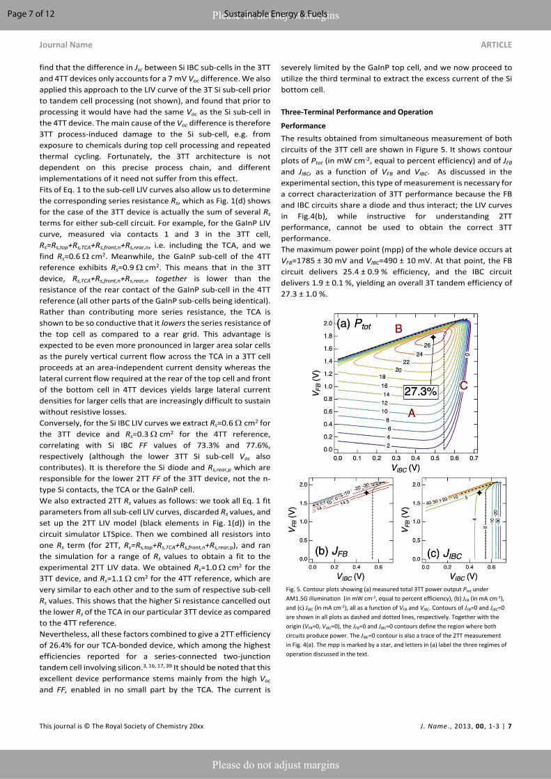
Performance The results obtained from simultaneous measurement of both circuits of the 3TT cell are shown in Figure 5. It shows contour plots of Ptot (in mW cm-2, equal to percent efficiency) and of JFB and JIBC, as a function of VFB and VIBC. As discussed in the experimental section, this type of measurement is necessary for a correct characterization of 3TT performance because the FB and IBC circuits share a diode and thus interact; the LIV curves in Fig.4(b), while instructive for understanding 2TT performance, cannot be used to obtain the correct 3TT performance. The maximum power point (mpp) of the whole device occurs at VFB=1785 ± 30 mV and VIBC=490 ± 10 mV. At that point, the FB circuit delivers 25.4 ± 0.9 % efficiency, and the IBC circuit delivers 1.9 ± 0.1 %, yielding an overall 3T tandem efficiency of 27.3 ± 1.0 %.
Fig. 5. Contour plots showing (a) measured total 3TT power output Ptot under AM1.5G illumination (in mW cm-2, equal to percent efficiency), (b) JFB (in mA cm-2), and (c) JIBC (in mA cm-2), all as a function of VFB and VIBC. Contours of JFB=0 and JIBC=0 are shown in all plots as dashed and dotted lines, respectively. Together with the origin (VFB=0, VIBC=0), the JFB=0 and JIBC=0 contours define the region where both circuits produce power. The JIBC=0 contour is also a trace of the 2TT measurement in Fig. 4(a). The mpp is marked by a star, and letters in (a) label the three regimes of operation discussed in the text.
Page 7 of 12 Sustainable Energy & Fuels
ARTICLE Journal Name
8 | J. Name., 2012, 00, 1-3 This journal is © The Royal Society of Chemistry 20xx
Please do not adjust margins
Please do not adjust margins
It is worth noting that the FB efficiency is reduced from the 2TT value of 26.4% when power is also extracted from the third terminal. During the 2TT measurement, the Si cell had to operate at the same current as the GaInP cell, and thus at a higher voltage than its mpp. Lowering the voltage of the Si cell from this operating point to its mpp reduces the efficiency in the FB circuit from 26.4% to 25.4%, but allows 1.9% to be collected in the IBC circuit, resulting in the higher total efficiency of 27.3%. This interaction between the circuits is why both circuits had to be measured simultaneously. The net efficiency increase of 0.9% ± 0.2% highlights the efficacy of this approach to extracting more power without resorting to middle contacts.
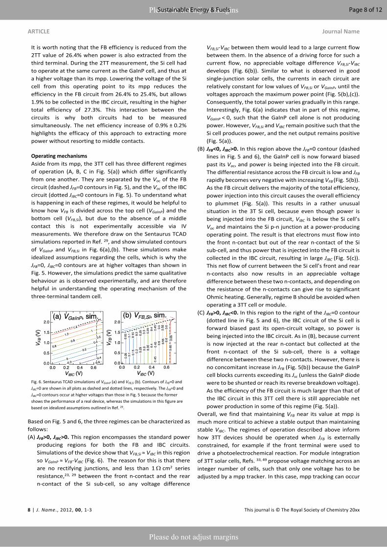
Operating mechanismsAside from its mpp, the 3TT cell has three different regimes of operation (A, B, C in Fig. 5(a)) which differ significantly from one another. They are separated by the Voc of the FB circuit (dashed JFB=0 contours in Fig. 5), and the Voc of the IBC circuit (dotted JIBC=0 contours in Fig. 5). To understand what is happening in each of these regimes, it would be helpful to know how VFB is divided across the top cell (VGaInP) and the bottom cell (VFB,Si), but due to the absence of a middle contact this is not experimentally accessible via IV measurements. We therefore draw on the Sentaurus TCAD simulations reported in Ref. 29, and show simulated contours of VGaInP and VFB,Si in Fig. 6(a),(b). These simulations make idealized assumptions regarding the cells, which is why the JFB=0, JIBC=0 contours are at higher voltages than shown in Fig. 5. However, the simulations predict the same qualitative behaviour as is observed experimentally, and are therefore helpful in understanding the operating mechanism of the three-terminal tandem cell.
Fig. 6. Sentaurus TCAD simulations of VGaInP (a) and VFB,Si (b). Contours of JFB=0 and JIBC=0 are shown in all plots as dashed and dotted lines, respectively. The JFB=0 and JIBC=0 contours occur at higher voltages than those in Fig. 5 because the former shows the performance of a real device, whereas the simulations in this figure are based on idealized assumptions outlined in Ref. 29.
Based on Fig. 5 and 6, the three regimes can be characterized as follows:(A) JFB>0, JIBC>0. This region encompasses the standard power
producing regions for both the FB and IBC circuits. Simulations of the device show that VFB,Si ≈ VIBC in this region so VGaInP ≈ VFB-VIBC (Fig. 6). The reason for this is that there are no rectifying junctions, and less than 1 cm2 series resistance,23, 29 between the front n-contact and the rear n-contact of the Si sub-cell, so any voltage difference
VFB,Si-VIBC between them would lead to a large current flow between them. In the absence of a driving force for such a current flow, no appreciable voltage difference VFB,Si-VIBC develops (Fig. 6(b)). Similar to what is observed in good single-junction solar cells, the currents in each circuit are relatively constant for low values of VFB,Si or VGaInP, until the voltages approach the maximum power point (Fig. 5(b),(c)). Consequently, the total power varies gradually in this range. Interestingly, Fig. 6(a) indicates that in part of this regime, VGaInP < 0, such that the GaInP cell alone is not producing power. However, VFB,Si and VIBC remain positive such that the Si cell produces power, and the net output remains positive (Fig. 5(a)).
(B) JFB<0, JIBC>0. In this region above the JFB=0 contour (dashed lines in Fig. 5 and 6), the GaInP cell is now forward biased past its Voc, and power is being injected into the FB circuit. The differential resistance across the FB circuit is low and JFB rapidly becomes very negative with increasing VFB (Fig. 5(b)). As the FB circuit delivers the majority of the total efficiency, power injection into this circuit causes the overall efficiency to plummet (Fig. 5(a)). This results in a rather unusual situation in the 3T Si cell, because even though power is being injected into the FB circuit, VIBC is below the Si cell’s Voc and maintains the Si p-n junction at a power-producing operating point. The result is that electrons must flow into the front n-contact but out of the rear n-contact of the Si sub-cell, and thus power that is injected into the FB circuit is collected in the IBC circuit, resulting in large JIBC (Fig. 5(c)). This net flow of current between the Si cell’s front and rear n-contacts also now results in an appreciable voltage difference between these two n-contacts, and depending on the resistance of the n-contacts can give rise to significant Ohmic heating. Generally, regime B should be avoided when operating a 3TT cell or module.
(C) JFB>0, JIBC<0. In this region to the right of the JIBC=0 contour (dotted line in Fig. 5 and 6), the IBC circuit of the Si cell is forward biased past its open-circuit voltage, so power is being injected into the IBC circuit. As in (B), because current is now injected at the rear n-contact but collected at the front n-contact of the Si sub-cell, there is a voltage difference between these two n-contacts. However, there is no concomitant increase in JFB (Fig. 5(b)) because the GaInP cell blocks currents exceeding its Jsc (unless the GaInP diode were to be shunted or reach its reverse breakdown voltage). As the efficiency of the FB circuit is much larger than that of the IBC circuit in this 3TT cell there is still appreciable net power production in some of this regime (Fig. 5(a)).
Overall, we find that maintaining VFB near its value at mpp is much more critical to achieve a stable output than maintaining stable VIBC. The regimes of operation described above inform how 3TT devices should be operated when JFB is externally constrained, for example if the front terminal were used to drive a photoelectrochemical reaction. For module integration of 3TT solar cells, Refs. 33, 49 propose voltage matching across an integer number of cells, such that only one voltage has to be adjusted by a mpp tracker. In this case, mpp tracking can occur
Page 8 of 12Sustainable Energy & Fuels
Journal Name ARTICLE
This journal is © The Royal Society of Chemistry 20xx J. Name., 2013, 00, 1-3 | 9
Please do not adjust margins
Please do not adjust margins
as in current modules, with the voltage in the FB circuits held at values near VFB,mpp per cell.In summary, utilization of a third rear terminal yields a substantial improvement in cell efficiency, and this effect is expected to be even greater in more strongly mismatched tandem cells. An improved annual yield as compared to 2TT devices, due to greater resilience to changes in the incident spectrum, has also been predicted,33, 50 and ultimately, 3TT cells have the potential to perform better than 4TT cells under AM1.5G due to reduced parasitic absorption and/or resistive losses.29
4 ConclusionsWe have fabricated a new type of hybrid tandem cell with three terminals, using a GaInP top cell and an IBC Si bottom cell with an additional front contact. The two cells were joined using a TCA consisting of silver coated microspheres embedded in epoxy, which can join rough surfaces through a low-temperature process with negligible series resistance. This has allowed us to achieve a two-terminal efficiency of 26.4 ± 1.0 % for a GaInP/Si cell, which is among the highest values reported for a series-connected two-junction tandem cell involving Si.3, 16,
17, 19, 39 The TCA approach is very versatile and thus likely to find application in a wide range of hybrid tandem cells, such as those involving perovskites.It was also demonstrated that by utilizing the third terminal of the 3TT cell, the efficiency could be increased by 0.9 ± 0.2 % absolute to 27.3 ± 1.0 %. The benefit of the third terminal is expected to be greatest for strongly current-mismatched sub-cells, enabling full power extraction from a wide variety of series-connected tandem cell materials and under changing spectral conditions. Rigorous characterization of 3TT performance was shown to require simultaneous measurement of both circuits, which revealed that the cell behaves much like two conventional cells when both produce power, but that large balancing currents and voltage losses can develop if one circuit produces power while the other does not. The 3TT cell architecture enables full power extraction with no middle terminals, which along with the TCA interconnect provides a powerful approach for the fabrication of highly efficient series-connected tandem cells with unprecedented flexibility in the selection of sub-cells.
5 Broader ContextPhotovoltaics (PV) is a rapidly growing market with the potential to provide clean energy covering much of the world’s energy demand. Module prices have dropped dramatically in recent years, but efficiency gains and cost savings have been incremental. The most powerful lever to further decrease the cost of PV electricity is increasing efficiency, as this lowers all area-dependent costs of a PV installation. This has stimulated intense research in tandem, or multijunction solar cells, where the solar spectrum is split across multiple solar cells to increase efficiency.
There are different configurations in which sub-cells can be assembled into tandem cells, with different trade-offs in terms of manufacturing complexity, efficiency, and annual energy yield. In this paper we demonstrate experimentally a novel three-terminal tandem cell configuration which achieves the high energy yield of four-terminal tandem cells while maintaining much of the simplicity of two-terminal tandem cells. We also present a transparent conductive adhesive with negligible resistance for facile integration of dissimilar sub-cells into a tandem cell, and use it demonstrate a 27.3% efficient tandem solar cell. These approaches provide unprecedented flexibility for the design of highly efficient solar cells.
6 Conflicts of interestThere are no conflicts to declare.
7 AcknowledgementsNREL authors acknowledge the support of Waldo Olavarria and Michelle Young for sample growth and processing (devices MP901, MQ339), Al Hicks for graphics support, Byungsul Min for providing refractive index data, Taylor Moot for transmission measurements, and Tom Moriarty for EQE and cell area measurements. The ISFH authors wish to thank Heike Kohlenberg, Guido Glowatzki and the processing team at ISFH for processing solar cells, and Robert Witteck for support with LTSpice simulations. This work was supported by the Alliance for Sustainable Energy, LLC, the manager and operator of the National Renewable Energy Laboratory for the U.S. Department of Energy (DOE) under Contract No. DE-AC36-08GO28308. Funding provided by the U.S. Department of Energy Office of Energy Efficiency and Renewable Energy Solar Energy Technologies Office under contract number DE-EE00030299. Funding for the work at ISFH was provided by the German Federal Ministry for Economic Affairs and Energy, under grant number 324040 (EASi), and by the European Union’s Seventh Framework Programme for research, technological development and demonstration within the “HERCULES” project (grant agreement No 608498). H. Schulte-Huxel acknowledges support for the Research Fellowship by Deutsche Forschungsgemeinschaft (DFG) (grant agreement No: SCHU 3206/1-1). The views expressed in the article do not necessarily represent the views of the DOE or the U.S. Government. The U.S. Government retains and the publisher, by accepting the article for publication, acknowledges that the U.S. Government retains a nonexclusive, paid-up, irrevocable, worldwide license to publish or reproduce the published form of this work, or allow others to do so, for U.S. Government purposes.
8 Notes and references
1. S. Essig, M. A. Steiner, C. Allebé, J. F. Geisz, B. Paviet-Salomon, S. Ward, A. Descoeudres, V. LaSalvia, L. Barraud, N. Badel, A. Faes, J. Levrat, M. Despeisse, C. Ballif, P. Stradins and D. L. Young, IEEE Journal of Photovoltaics, 2016, 6, 1012-1019.
Page 9 of 12 Sustainable Energy & Fuels

ARTICLE Journal Name
10 | J. Name., 2012, 00, 1-3 This journal is © The Royal Society of Chemistry 20xx
Please do not adjust margins
Please do not adjust margins
2. M. A. Green, Nature Energy, 2016, 1, 15015.3. M. A. Green, Y. Hishikawa, E. D. Dunlop, D. H. Levi, J. Hohl-
Ebinger, M. Yoshita and A. W. Y. Ho-Baillie, Progress in Photovoltaics: Research and Applications, 2019, 27, 3-12.
4. A. Richter, M. Hermle and S. W. Glunz, IEEE Journal of Photovoltaics, 2013, 3, 1184-1191.
5. M. A. Green, Proc. of SPIE Vol. 8981, San Francisco, CA, USA, 2014.
6. J. Werner, B. Niesen and C. Ballif, Advanced Materials Interfaces, 2018, 5, 1700731.
7. Z. Yu, M. Leilaeioun and Z. Holman, Nature Energy, 2016, 1, 16137.
8. W. Shockley and H. J. Queisser, Journal of Applied Physics, 1961, 32, 510-519.
9. M. A. Green, Third generation photovoltaics - advanced solar energy conversion, Springer, Berlin, Heidelberg, New York, 2003.
10. I. Almansouri, A. Ho-Baillie, S. P. Bremner and M. A. Green, Photovoltaics, IEEE Journal of, 2015, 5, 968 - 976.
11. Z. J. Yu, J. V. Carpenter and Z. C. Holman, Nature Energy, 2018, 3, 747-753.
12. R. Jones-Albertus, D. Feldman, R. Fu, K. Horowitz and M. Woodhouse, Progress in Photovoltaics: Research and Applications, 2016, 24, 1272-1283.
13. S. Essig, C. Allebé, T. Remo, J. F. Geisz, M. A. Steiner, K. Horowitz, L. Barraud, J. S. Ward, M. Schnabel, A. Descoeudres, D. L. Young, M. Woodhouse, M. Despiesse, C. Ballif and A. Tamboli, Nature Energy, 2017, 2, 17144.
14. T. Duong, Y. Wu, H. Shen, J. Peng, X. Fu, D. Jacobs, E. C. Wang, T. C. Kho, K. C. Fong, M. Stocks, E. Franklin, A. Blakers, N. Zin, K. McIntosh, W. Li, Y. B. Cheng, T. P. White, K. Weber and K. Catchpole, Advanced Energy Materials, 2017, 7, 1700228.
15. S. Essig, S. Ward, M. A. Steiner, D. J. Friedman, J. F. Geisz, P. Stradins and D. L. Young, Energy Procedia, 2015, 77, 464-469.
16. K. A. Bush, S. Manzoor, K. Frohna, Z. J. Yu, J. A. Raiford, A. F. Palmstrom, H.-P. Wang, R. Prasanna, S. F. Bent, Z. C. Holman and M. D. McGehee, ACS Energy Letters, 2018, 3, 2173-2180.
17. B. Chen, Z. Yu, K. Liu, X. Zheng, Y. Liu, J. Shi, D. Spronk, P. N. Rudd, Z. Holman and J. Huang, Joule, 2019, 3, 177-190.
18. F. Sahli, J. Werner, B. A. Kamino, M. Bräuninger, R. Monnard, B. Paviet-Salomon, L. Barraud, L. Ding, J. J. Diaz Leon, D. Sacchetto, G. Cattaneo, M. Despeisse, M. Boccard, S. Nicolay, Q. Jeangros, B. Niesen and C. Ballif, Nature Materials, 2018, 17, 820-826.
19. Oxford PV, Oxford PV perovskite solar cell achieves 28% efficiency, https://www.oxfordpv.com/news/oxford-pv-perovskite-solar-cell-achieves-28-efficiency, (accessed December 20th, 2018).
20. S. Essig, O. Moutanabbir, A. Wekkeli, H. Nahme, E. Oliva, A. W. Bett and F. Dimroth, Journal of Applied Physics, 2013, 113, 203512.
21. E. Veinberg-Vidal, L. Vauche, K. Medjoubi, C. Weick, C. Besançon, P. Garcia-Linares, A. Datas, A. Kaminski-Cachopo, P. Voarino, P. Mur, J. Decobert and C. Dupré, Progress in Photovoltaics: Research and Applications, 2019, 27, 652-661.
22. R. Cariou, J. Benick, F. Feldmann, O. Höhn, H. Hauser, P. Beutel, N. Razek, M. Wimplinger, B. Bläsi, D. Lackner, M. Hermle, G. Siefer, S. W. Glunz, A. W. Bett and F. Dimroth, Nature Energy, 2018, 3, 326-333.
23. M. Rienäcker, E. L. Warren, M. Schnabel, H. Schulte-Huxel, R. Niepelt, R. Brendel, P. Stradins, A. C. Tamboli and R. Peibst, Progress in Photovoltaics: Research and Applications, 2019, 27, 410-423.
24. T. R. Klein, B. G. Lee, M. Schnabel, E. L. Warren, P. Stradins, A. C. Tamboli and M. F. A. M. van Hest, ACS applied materials & interfaces, 2018, 10, 8086-8091.
25. T. R. Klein, M. Schnabel, E. L. Warren, B. G. Lee, P. Stradins, A. Tamboli and M. F. A. M. van Hest, Proceedings of the 44th IEEE PVSC, Washington D.C., USA, 2017.
26. T. Sameshima, J. Takenezawa, M. Hasumi, T. Koida, T. Kaneko, M. Karasawa and M. Kondo, Jpn J Appl Phys 1, 2011, 50, 052301.
27. J. Yang, Z. Peng, D. Cheong and R. Kleiman, 2012.28. M. Schnabel, M. Rienäcker, E. L. Warren, J. F. Geisz, R. Peibst, P.
Stradins and A. C. Tamboli, IEEE Journal of Photovoltaics, 2018, 8, 1584-1589.
29. E. L. Warren, M. G. Deceglie, M. Rienacker, R. Peibst, A. C. Tamboli and P. Stradins, Sustainable Energy & Fuels, 2018, 2, 1141-1147.
30. T. Nagashima, K. Hokoi, K. Okumura and M. Yamaguchi, Proceedings of the 4th World Conference on Photovoltaic Energy Conversion, Waikoloa, HI, USA, 2006.
31. T. Nagashima, K. Okumura, K. Murata and Y. Kimura, Proceedings of the 28th IEEE PVSC, Anchorage, AK, USA, 2000.
32. Z. Djebbour, W. El-Huni, A. Migan Dubois and J.-P. Kleider, Progress in Photovoltaics: Research and Applications, 2019, 27, 306-315.
33. J. M. Gee, Solar Cells, 1988, 24, 147-155.34. S. Sakai and M. Umeno, Journal of Applied Physics, 1980, 51,
5018-5024.35. S. Sista, Z. Hong, M.-H. Park, Z. Xu and Y. Yang, Advanced
Materials, 2010, 22, E77-E80.36. T. Soga, M. Yang, T. Jimbo and M. Umeno, Jpn J Appl Phys 1, 1996,
35, 1401.37. M. A. Steiner, M. W. Wanlass, J. J. Carapella, A. Duda, J. S. Ward,
T. E. Moriarty and K. A. Emery, Progress in Photovoltaics: Research and Applications, 2009, 17, 587-593.
38. A. Martí, E. Antolín, P. García-Linares, E. López, J. Villa and I. Ramiro, physica status solidi c, 2017, 14, 1700191.
39. N. Jain and M. K. Hudait, Energy Harvesting and Systems, 2014, 1, 121-145.
40. J. F. Geisz, M. A. Steiner, I. García, S. R. Kurtz and D. J. Friedman, Applied Physics Letters, 2013, 103, 041118.
41. J. L. Young, M. A. Steiner, H. Döscher, R. M. France, J. A. Turner and Todd G. Deutsch, Nature Energy, 2017, 2, 17028.
42. M. Rienäcker, M. Bossmeyer, A. Merkle, U. Römer, F. Haase, J. Krügener, R. Brendel and R. Peibst, IEEE Journal of Photovoltaics, 2017, 7, 11-18.
43. C. R. Osterwald, K. A. Emery, D. R. Myers and R. E. Hart, Conference Record of the 21st IEEE PVSC, Kissimmee, FL, USA, 1990.
44. R. L. Mueller, Solar Energy Materials and Solar Cells, 1993, 30, 37-45.
45. M. A. Steiner, J. F. Geisz, T. E. Moriarty, R. M. France, W. E. McMahon, J. M. Olson, S. R. Kurtz and D. J. Friedman, IEEE Journal of Photovoltaics, 2013, 3, 879-887.
46. M. Schnabel, T. R. Klein, N. Jain, S. Essig, H. Schulte-Huxel, E. Warren, M. F. A. M. van Hest, J. Geisz, P. Stradins, A. Tamboli, M. Rienacker, A. Merkle, J. Schmidt, R. Brendel and R. Peibst, Proceedings of the 44th IEEE PVSC, Washington D.C, USA, 2017.
47. M. Rienäcker, M. Schnabel, E. Warren, A. Merkle, H. Schulte-Huxel, T. R. Klein, M. F. A. M. v. Hest, M. A. Steiner, J. Geisz, S. Kajari-Schröder, R. Niepelt, J. Schmidt, R. Brendel, P. Stradins, A. Tamboli and R. Peibst, Proceedings of the 33rd EU PVSEC, Amsterdam, Netherlands, 2017.
Page 10 of 12Sustainable Energy & Fuels

Journal Name ARTICLE
This journal is © The Royal Society of Chemistry 20xx J. Name., 2013, 00, 1-3 | 11
Please do not adjust margins
Please do not adjust margins
48. W. F. Holmgren, C. W. Hansen and M. A. Mikofski, The Journal of Open Source Software, 2018, 3, 884.
49. H. Schulte-Huxel, E. L. Warren, M. Schnabel, P. Stradins, D. J. Friedman and A. C. Tamboli, Proceedings of the 44th IEEE PVSC, Washington D.C., USA, 2017.
50. H. Schulte-Huxel, T. J. Silverman, M. G. Deceglie, D. J. Friedman and A. C. Tamboli, IEEE Journal of Photovoltaics, 2018, 8, 1376-1383.
Page 11 of 12 Sustainable Energy & Fuels

Three-Terminal III-V/Si Tandem Solar Cells Enabled by a Transparent Conductive Adhesive
Manuel Schnabel,*a Henning Schulte-Huxel,a,b Michael Rienäcker,b Emily L. Warren,a Paul F. Ndione,a Bill Nemeth,a Talysa R. Klein,a Maikel F.A.M. van Hest,a John F. Geisz,a Robby Peibst,b Paul Stradins,a Adele C. Tambolia
aNational Renewable Energy Laboratory, Golden CO 80401, USAbInstitute for Solar Energy Research Hamelin, D-31860 Emmerthal, Germany
TABLE OF CONTENTS FIGURE AND CAPTION
Three-terminal tandem solar cell with conductive adhesive interconnect and back-contacted bottom cell delivers 27.3% efficiency.
Page 12 of 12Sustainable Energy & Fuels


![CHAPTER 6 Mycobacterium tuberculosis PPE/MPTR ORF, Rv2608 ...shodhganga.inflibnet.ac.in/bitstream/10603/25593/13/13_chapter6.pdf · Polymorphic Tandem Repeats] in the C-terminal region](https://img.dokumen.tips/doc/110x75/5fd9a6d1f6093f126a3b11d6/chapter-6-mycobacterium-tuberculosis-ppemptr-orf-rv2608-polymorphic-tandem.jpg)