Embed Size (px)
Citation preview
Three-dimensional ferroelectric domain imaging of epitaxial BiFeO3 thinfilms using angle-resolved piezoresponse force microscopy
Moonkyu Park,1,3 Seungbum Hong,1,a� Jeffrey A. Klug,1,4 Michael J. Bedzyk,1,4,5
Orlando Auciello,1,2 Kwangsoo No,3,a� and Amanda Petford-Long2
1Materials Science Division, Argonne National Laboratory, Argonne, Illinois 60439, USA2Center for Nanoscale Materials, Argonne National Laboratory, Argonne, Illinois 60439, USA3Department of Materials Science and Engineering, Korea Advanced Institute of Science and Technology,Daejeon 305-701, Republic of Korea4Department of Physics and Astronomy, Northwestern University, Illinois 60208, USA5Department of Materials Science, Northwestern University, Illinois 60208, USA
�Received 12 May 2010; accepted 16 August 2010; published online 17 September 2010�
Here we introduce angle-resolved piezoresponse force microscopy �AR-PFM�, whereby the sampleis rotated by 30° increments around the surface normal vector and the in-plane PFM phase signalsare collected at each angle. We obtained the AR-PFM images of BaTiO3 single crystal andcube-on-cube epitaxial �001� BiFeO3 �BFO� thin film on SrRuO3 /SrTiO3 substrate, and confirmedthat the AR-PFM provides more unambiguous information on the in-plane polarization directionsthan the conventional PFM method. Moreover, we found eight additional in-plane polarizationvariants in epitaxial BFO thin films, which are formed to mitigate highly unstable charged domainboundaries. © 2010 American Institute of Physics. �doi:10.1063/1.3487933�
Ferroelectric oxide materials provide a unique platformto enable the next generation memory devices, using theirswitchable polarization and integration of ferroelectricnanocapacitors.1 Until now, the SrBi2Ta2O9 �SBT� �Refs. 2and 3� and Pb�ZrxTi1−x�O3 �PZT� �Ref. 3� family of materialshave served as the cornerstone for applications in non-volatile memories and piezoelectric actuators �PZT�. Acritical drawback of SBT is the relatively low polarization��30 �C /cm2� �Refs. 2 and 3� while the problem with PZTis the presence of lead. In this respect, the lead-free ferro-electric BiFeO3 �BFO� has attracted a great deal of attentionbecause of its superior polarization ��120 �C /cm2�,4,5
which is comparable to that of the tetragonal, Ti-rich PZTfilms.
However, BFO thin films exhibit high leakage currents,6
where oxygen vacancies7 and/or the unusual electronic trans-port through ferroelectric domain walls are the main cause.8
Hong et al.9 also observed the emergence of charged domainboundaries �CDBs� in round-shaped BFO nanostructures,which contributed to leaky piezoresponse hysteresis loops.While the leakage paths formed at the CDBs ��P·n�0� inBFO have been reported, it is still not clear why the CDBsform and how they affect the piezoresponse at the nanoscale.Therefore, an in-depth investigation of the domain structureby piezoresponse force microscopy �PFM� in BFO thin filmsis required, which helps us understand the mechanism ofpolarization switching and electrical properties. However,constructing three-dimensional PFM images of polarizationdomains has been a great challenge because sliding of the tipand cantilever buckling influence the PFM signals.10,11
Here we introduce a polarization domain imaging tech-nique named angle-resolved piezoresponse force microscopy�AR-PFM�, present direct observation of CDBs and interme-diate polarization variants in epitaxially grown BFO thin
films, and discuss the correlation between the resulting do-main configuration and the film growth mechanism.
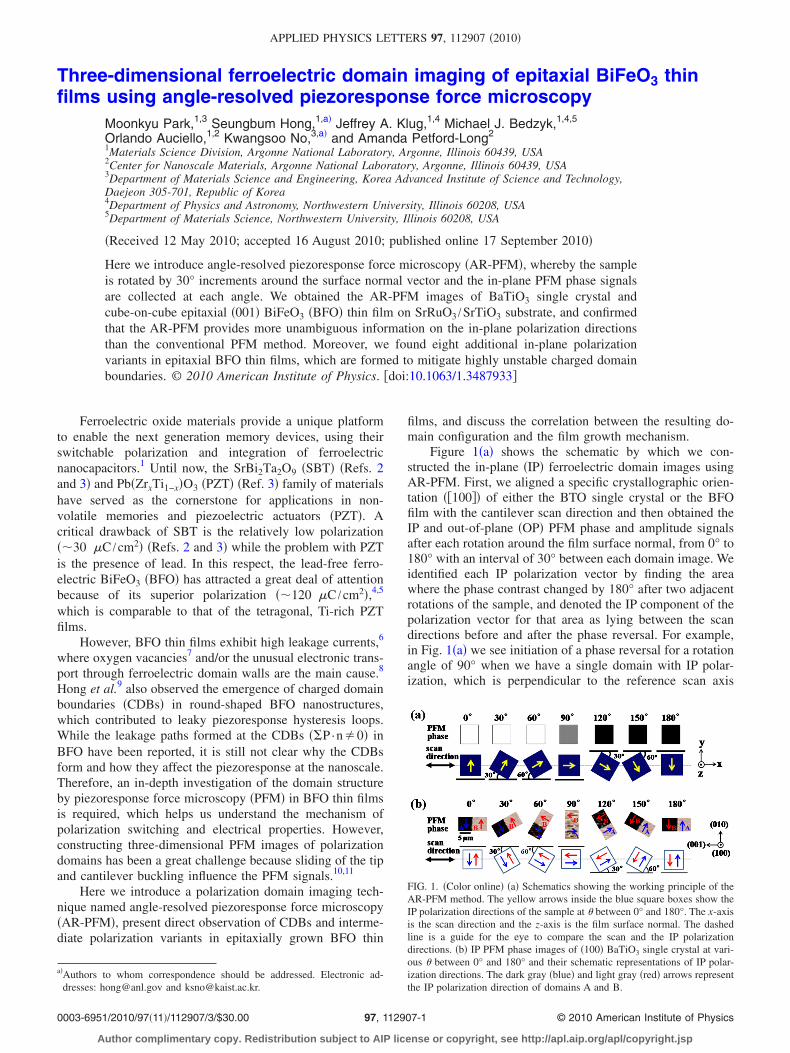
Figure 1�a� shows the schematic by which we con-structed the in-plane �IP� ferroelectric domain images usingAR-PFM. First, we aligned a specific crystallographic orien-tation ��100�� of either the BTO single crystal or the BFOfilm with the cantilever scan direction and then obtained theIP and out-of-plane �OP� PFM phase and amplitude signalsafter each rotation around the film surface normal, from 0° to180° with an interval of 30° between each domain image. Weidentified each IP polarization vector by finding the areawhere the phase contrast changed by 180° after two adjacentrotations of the sample, and denoted the IP component of thepolarization vector for that area as lying between the scandirections before and after the phase reversal. For example,in Fig. 1�a� we see initiation of a phase reversal for a rotationangle of 90° when we have a single domain with IP polar-ization, which is perpendicular to the reference scan axis
a�Authors to whom correspondence should be addressed. Electronic ad-dresses: [email protected] and [email protected].
FIG. 1. �Color online� �a� Schematics showing the working principle of theAR-PFM method. The yellow arrows inside the blue square boxes show theIP polarization directions of the sample at � between 0° and 180°. The x-axisis the scan direction and the z-axis is the film surface normal. The dashedline is a guide for the eye to compare the scan and the IP polarizationdirections. �b� IP PFM phase images of �100� BaTiO3 single crystal at vari-ous � between 0° and 180° and their schematic representations of IP polar-ization directions. The dark gray �blue� and light gray �red� arrows representthe IP polarization direction of domains A and B.
APPLIED PHYSICS LETTERS 97, 112907 �2010�
0003-6951/2010/97�11�/112907/3/$30.00 © 2010 American Institute of Physics97, 112907-1
Author complimentary copy. Redistribution subject to AIP license or copyright, see http://apl.aip.org/apl/copyright.jsp

�0°�. The AR-PFM technique therefore allows us to deter-mine all the IP polarization directions within the angular res-olution of each step �30° in this study� without relying onPFM amplitude information.
We used the AR-PFM technique to study the polarizationdomains of a �100� BaTiO3 single crystal �MTI Corporation�as a standard example to check whether we can reliably iden-tify the IP polarization directions.12 We chose a region com-
prised of �01̄0� �region A� and �010� �region B� polarizationvariants and rotated the region by 30° between recordingeach set of images �Fig. 1�b��. Here we defined the angle ofsample rotation, �, as that between the cantilever long axisand the �001� direction. We found that the phase reversaloccurred near �=90° in both regions A and B, which verifiesthat AR-PFM can unambiguously determine the IP polariza-tions within the resolution of each angular step.
We plotted the average IP and OP PFM phase and am-plitude values over the whole area in regions A and B in Fig.1�b�, as a function of � �Figs. 2�a�–2�d��. As expected, theOP PFM amplitude and phase values in both regions re-mained constant regardless of � because the OP piezore-sponse component does not change with IP rotation of thesample �Figs. 2�a� and 2�b��. However, the IP PFM ampli-tude deviated from its expected dependence on � �see Fig.2�c��. This discrepancy will lead to inaccurate domain im-ages if we use the amplitude and phase of IP PFM images toreconstruct the polarization directions in the domains. ThePFM phase information, however, is relatively stable andbehaves more consistently with the theory �Fig. 2�d��. There-fore, AR-PFM, which is based on the PFM phase contrastand �, is expected to yield a more accurate picture of IPdomain polarization vectors.
We fabricated BFO multiferroic thin films to identify theferroelectric polarization variants using the AR-PFMmethod. BFO thin films �40 nm thick� were grown by rfmagnetron sputtering �AJA International, Rapier Series� at680 °C over a 120 nm thick SrRuO3 �SRO� �001� bottomelectrodes deposited on SrTiO3 �STO� �001� substrates at680 °C. X-ray diffraction �XRD� Phi scans of the BFO,
SRO, and STO �202� family of reflections confirmed cube-on-cube epitaxy for both the BFO and SRO films �Fig. 3�a��.The �-2� scan also showed that the BFO and SRO films areboth pseudocubic �001� oriented �Fig. 3�b��. The XRD analy-sis showed that there was no IP rotation of the crystals, sug-gesting there would be no associated IP polarization rotation.
There was a small amount of Fe2O3 impurity present inthe films, as seen from the �-2� XRD scan, which is consis-tent with the faceted islands that are seen in the atomic forcemicroscopy �AFM� topography image �Fig. 3�c��, and is inagreement with recent findings that the BFO and Fe2O3phases coexist when BFO thin films are grown at oxygenpressures below or equal to 5 mTorr.13 In order to avoid anyspurious effects caused by the Fe2O3 phase and surface mor-phology, we chose to analyze a flat area of 1.17�0.74 �m2, which is free of Fe2O3, when acquiring theAR-PFM domain images �Fig. 3�d��.
We verified the IP polarization variants of the BFO thinfilm using AR-PFM �Fig. 4�. The region in which the phasechanged by 180° after a rotation step of 30° was painted witha different color on each IP PFM phase image. Since the OPPFM signals showed a uniform downward polarization ori-entation for all the angular steps,12 we could map all thepolarization by superimposing the regions where the phasesignals changed by 180° at each angular step �Fig. 4�a��. Asa result, we identified twelve polarization variants in BFOthin films whereas a number of studies have reported that
FIG. 2. �Color online� OP PFM �a� amplitude and �b� phase, and IP PFM �c�amplitude and �d� phase values of �100� BaTiO3 single crystal as a functionof �. Dark gray �blue� triangle and light gray �red� square represent theexperimentally measured values of domains A and B in Fig. 1�b�, respec-tively. The dark gray �blue� dashed line and light gray �red� solid line showthe calculated values for domains A and B, respectively.
FIG. 3. �Color online� �a� IP and �b� OP XRD plots of �001� BiFeO3 thinfilm grown on �001� SRO/�001� STO substrate. AFM topography images of�c� �001� BiFeO3 thin film and �d� the selected area for AR-PFM domainimage acquisitions.
FIG. 4. �Color online� �a� IP domain configuration of BiFeO3 thin film.Local ferroelectric domain configurations constructed by ��b� and �d�� con-ventional PFM and ��c� and �e�� AR-PFM in the regions A ��b� and �c�� andB ��d� and �e�� in Fig. 4�a�. Dark gray �blue� and light gray �red� linesrepresent neutral and CDBs, respectively.
112907-2 Park et al. Appl. Phys. Lett. 97, 112907 �2010�
Author complimentary copy. Redistribution subject to AIP license or copyright, see http://apl.aip.org/apl/copyright.jsp

BFO can only have up to eight polarization variants lyingalong the �111� directions.14,15 This result shows that theepitaxial BFO thin films used in this study have regions withpolarization variants deviating from the �111� directions,which are the easy polarization axes analogous to easy mag-netization axes.15 Without using the AR-PFM technique, itwould have been difficult to find those intermediate polariza-tion variants due to the large errors in amplitude signals ob-tained using conventional lateral PFM.10
In order to understand the origin of intermediate polar-ization variants and study the local distribution of ferroelec-tric domains, we constructed the domain map of the regions�A� and �B� in Fig. 4�a� using the conventional PFM �Figs.4�b� and 4�d�� and the AR-PFM methods �Figs. 4�c� and4�e��. Imaging of the domain configuration by the conven-tional PFM method, based on the assumption of four IP po-larization variants, showed a large portion of CDBs thatwould be very unstable due to the increase in the electro-static energy at the boundaries. The proportion of CDBs was86.3% in region A and 80.2% in region B, respectively, inFigs. 4�b� and 4�d�. However, when constructing the domainconfiguration from our AR-PFM data, the proportion ofCDBs decreased to 63.3% in region A and 43.6% in region B�Figs. 4�c� and 4�e��. In addition to the decrease in the por-tion of CDBs, the amount of charging along the CDBs wouldalso decrease due to the smaller angle between the neighbor-ing polarization variants separated by the CDBs.
It is relevant to discuss the possible origin of the CDBsand their impact on the ferroelectric properties of BFO films.Since BFO has a Curie temperature �1100 K� above thegrowth temperature �953 K�, BFO nuclei formed during theinitial stages in film growth, larger than the critical size �e.g.,4.2 nm for PbTiO3 particles� �Ref. 16� to exhibit polariza-tion, will have their own ferroelectric polarization variantswhen they are deposited on the SRO/STO substrate. At thisstage, stable polarization vectors pointing along �111� direc-tions are induced by the rhombohedral crystal symmetry ofthe nuclei. As the film grows first in an island mode, eachisland with its polarization variant will not interact with theneighboring ones and grow independently, preserving theirpolarization variants, until they touch each other. It is highlylikely that in this process many of the polarization directionsin the grains will not be able to fully switch to form a neutralboundary with the adjacent regions and so CDBs will form.We believe that the intermediate polarization variants, whichdeviate from the easy axes imposed by the rhombohedralcrystal symmetry, are formed to act as mitigating regions todecrease the electrostatic energy at the CDBs, as in the caseof vortex domain configuration.17 The CDBs that remaineven after the formation of the intermediate variants are ex-pected to be the dominant sources of imprint and high leak-age properties in the films.
It could be argued that when the ferroelectric islandswere initially deposited on the substrate they would have nopreferred IP polarization direction because of the pseudocu-bic symmetry, which is not the case if the film was grown ina layer by layer deposition mode where the initial preferen-tial polarization variants would dominate the domain pattern.In order to check the validity of our results, we analyzed theareal fraction of each IP polarization direction �Fig. 4�a��. Wefound that the relative fractions of domains with positive
��010�� and negative ��01̄0�� y-axis IP polarization vector
components were 42% and 58%, respectively, whereas those
of domains with positive ��100�� and negative ��1̄00�� x-axisIP polarization vector components were 57% and 43%, re-spectively. These findings support the hypothesis that theferroelectric domains did not have a significant preference toa specific polarization direction at initial growth stage.
In conclusion, we found 12 IP polarization variants in anepitaxially grown, �001� BFO thin film on SRO/STO sub-strates, using the AR-PFM method. The emergence of theadditional variants deviating from the so-called ferroelectriceasy axes, which are formed to mitigate highly unstableCDBs, lead to formation of continuous domain structure re-sembling Neel type domain walls, where the polarizationvariants rotate around the vector normal to them.
The submitted manuscript has been created by UChicagoArgonne, LLC, Operator of Argonne National Laboratory�“Argonne”�. Argonne, a U.S. Department of Energy Officeof Science laboratory, is operated under Contract No. DE-AC02-06CH11357. The U. S. Government retains for itself,and others acting on its behalf, a paid-up nonexclusive, irre-vocable worldwide license in said article to reproduce, pre-pare derivative works, distribute copies to the public, andperform publicly and display publicly, by or on behalf of theGovernment. The XRD facility at NU is supported by MR-SEC Grant No. DMR-0520513 from the National ScienceFoundation. M.P. and K.N. acknowledge the financial sup-port by Mid-career Researcher Program �Grant No. 2010-0015063� and Nano R&D Program �Grant No. 2009-0081946� through NRF grant funded by the MEST. We thankProfessor A. Gruverman at University of Nebraska for hiscritical reading of our manuscript.
1C. H. Ahn, K. M. Rabe, and J. M. Triscone, Science 303, 488 �2004�.2J. F. Scott and C. Paz de Araujo, Science 246, 1400 �1989�.3O. Auciello, J. F. Scott, and R. Ramesh, Phys. Today 51�7�, 22 �1998�.4J. Wu and J. Wang, J. Appl. Phys. 106, 104111 �2009�.5J. Wang, J. B. Neaton, H. Zheng, V. Nagarajan, S. B. Ogale, B. Liu, D.Viehland, V. Vaithyanathan, D. G. Schlom, U. V. Waghmare, N. A.Spaldin, K. M. Rabe, M. Wuttig, and R. Ramesh, Science 299, 1719�2003�.
6J. Dho, X. Qi, H. Kim, J. L. MacManus-Driscoll, and M. G. Blamire, Adv.Mater. 18, 1445 �2006�.
7S. K. Singh, K. Maruyama, and H. Ishiwara, Appl. Phys. Lett. 91, 112913�2007�.
8J. Seidel, L. W. Martin, Q. He, Q. Zhan, Y.-H. Chu, A. Rother, M. E.Hawkridge, P. Maksymovych, P. Yu, M. Gajek, N. Balke, S. V. Kalinin, S.Gemming, F. Wang, G. Catalan, J. F. Scott, N. A. Spaldin, J. Orenstein,and R. Ramesh, Nature Mater. 8, 229 �2009�.
9S. Hong, J. A. Klug, M. Park, A. Imre, M. J. Bedzyk, K. No, A. Petford-Long, and O. Auciello, J. Appl. Phys. 105, 061619 �2009�.
10S. V. Kalinin, B. J. Rodriguez, S. Jesse, J. Shin, A. P. Baddorf, P. Gupta, H.Jain, D. B. Williams, and A. Gruverman, Microsc. Microanal. 12, 206�2006�.
11R. Nath, S. Hong, J. A. Klug, A. Imre, M. J. Bedzyk, R. S. Katiyar, and O.Auciello, Appl. Phys. Lett. 96, 163101 �2010�.
12See supplementary material at http://dx.doi.org/10.1063/1.3487933 for de-tailed experimental conditions of PFM measurements.
13M. Murakami, S. Fujino, S.-H. Lim, L. G. Salamanca-Riba, M. Wuttig, I.Takeuchia, B. Varughese, H. Sugaya, T. Hasegawa, and S. E. Lofland,Appl. Phys. Lett. 88, 112505 �2006�.
14F. Zavaliche, P. Shafer, R. Ramesh, M. P. Cruz, R. R. Das, D. M. Kim, andC. B. Eom, Appl. Phys. Lett. 87, 252902 �2005�.
15Y. Chu, L. W. Martin, M. B. Holcomb, and R. Ramesh, Mater. Today 10,16 �2007�.
16W. L. Zhong, Y. G. Wang, P. L. Zhang, and B. D. Qu, Phys. Rev. B 50,698 �1994�.
17A. Gruverman, D. Wu, H.-J. Fan, I. Vrejoiu, M. Alexe, R. J. Harrison, andJ. F. Scott, J. Phys.: Condens. Matter 20, 342201 �2008�.
112907-3 Park et al. Appl. Phys. Lett. 97, 112907 �2010�
Author complimentary copy. Redistribution subject to AIP license or copyright, see http://apl.aip.org/apl/copyright.jsp