Embed Size (px)
Citation preview


2 2 January 2008
This Presentation Contains
•Background /History of Cerium Laboratories
•Overview of Capability and Services
•Overview of Selected Techniques

3 3
Introduction to Cerium Laboratories LLC
• Located in the heart of Silicon Hills – Austin, Texas
• Created in 1986 as an in house process characterization laboratory for Advanced Micro Devices Inc.
• Supported world wide efforts for AMD, including technology development and insertions into manufacturing sites in Japan, Europe, and the US.
• Providing commercial services since 2004
• Division was spun-off to form Cerium Laboratories, LLC
• Specializing in device characterization and process analysis service for Semiconductor Industry

4 4 January 2008
FAB25
Introduction to Cerium Laboratories LLC
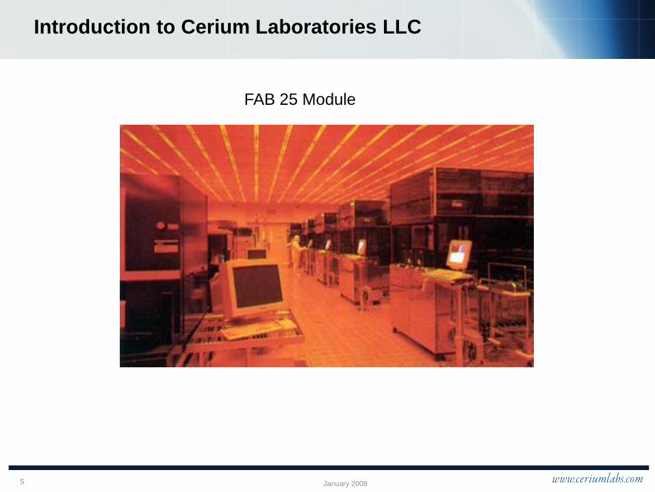
5 5 January 2008
FAB 25 Module
Introduction to Cerium Laboratories LLC

6 6 January 2008
PCAL Manager- Donald Tiffin
Introduction to Cerium Laboratories LLC

7 7 January 2008
AES Auger Electron Spectroscopy
AFM Atomic Force Microscopy
BSE Back-Scattered Electron microscopy
DMS Defect Management System
EDS Electron Dispersive Spectroscopy ESCA Electron Spectroscopy for Chemical Analysis
FIB Focused ion beam
FTIR Fourier Transformed Infrared Spec
GC-MS Gas Chromatography – Mass Spec
IC Ion Chromatography
ICP-MS Inductively Coupled Plasma- Mass Spec
μ-RS Micro-Raman Spectroscopy
SEM Scanning Electron Microscopy
SIMS Secondary-Ion Mass Spectroscopy
SRP Spreading Resistance Probe TEM Transmission Electron Microscopy
TOF-SIMS Time-Of-Flight Secondary-Ion Mass Spectroscopy
TXRF Total reflection X-ray Fluorescence
VPD Vapor Phase Decomposition
WD-XRF Wavelength Dispersive X-ray Fluorescence
XPS X-ray Photoelectron Spectroscopy
XRD X-ray Diffraction
XRR X-ray Reflectivity
Introduction to Cerium Laboratories LLC: Technologies

8 8
Introduction to Cerium Laboratories LLC
• Cerium has over 150 customers, including those designing
or manufacturing: EPROM, ASIC, DRAM, SRAM, FLASH,
Microprocessors, Embedded Logic, DSP, MEMS, LED,
and RF devices using CMOS and Bi-Polar semiconductor
technologies.
• Cerium provides services across the electronics industry
value chain;
Material Suppliers
Wafer Manufacturers
Equipment Manufacturers
Chip Manufacturers
Final Test Firms
Design houses

9 9
• Areas of expertise include
Electron Microscopy - nano-scale characterization SEM, TEM, FIB, AFM, and optical microscopy
Elemental analysis with EDS and EELS
Spectroscopy - high resolution elemental analysis of films SIMS, Auger, XPS, Raman, FTIR, XRD, XRR, WDXRF
Analytical Chemistry – chemical and contamination analysis VPD-ICPMS, HR-ICPMS,GCMS, IC, ICPOES, TOC, Assay
Enviromental testing (air, water and surface contamination)
• Cerium employs over 25 scientists and engineers with an average of over 15 years of professional experience in the semiconductor industry.
Cerium Labs Infrastructure

10 10
Diversified Expertise
• Reliability issues due to cosmic ray neutron
• Chemical analysis of Solar Poly Si impurities
• VPD analysis for Si wafer
• Reverse Engineering

11 11
Data and Sample Security
NDA - Cerium regards every clients data as proprietary and confidential.
Standard practice includes entering into bi-lateral non-disclosure agreements with our customers
Acquired data is not repackaged and offered as commercial reports
Secured Environment:
Two layers of security controlled access to the facilities
128-bit encrypted database and IT data transfer infrastructure
LabCollector™ Database:
Custom tailored application designed by Cerium Labs
Audit trail
Chain of custody
Facilitates analyst/client dialogue
128-bit encrypted web based data access appliance

12 12
Data and Sample Security
Cerium Laboratories has worked with clients from the fortune
500 list, National Laboratories and Universities to
innovative start up companies.
The wide range of characterization capability allows for the
necessary insight and understanding of material properties
and their effect in products and applications.
The synergistic combination of Cerium’s advanced electron
imaging, surface science and analytical chemistry labs
enables the development of solutions to material R&D.

13 13
Industry and Technology served
Semiconductor Alternative Energy
Silicon Manufacturers Solar ( Si, CIGS,CdTe)
Equipment Manufacturers Hydrogen Fuel Cell
Chip Manufacturers Solid Oxide Fuel Cell
Design and Test Houses Lithium-Ion Technologies
Reverse Engineering Organic
Reliability Issues from cosmic rays
neutrons
Chemical analysis of solar grade Si
•We provide services to a wide range of sectors within the semiconductor and alternative energy industries.

14 14
REVERSE ENGINEERING

15 15
Reverse Engineering and Litigation Support
Cerium experts have experience in IP/Patent case support:
From Reverse Engineering needed to prepare licensing campaign,
evidence evaluation during discovery process, through depositions and expert
testimony while in litigation.
Cerium experts have experience in high-technology manufacturing, R&D, and analysis.
Support of semi, pharmaceutical, nanotechnology, and various fuel cell lines including
Solar, Hydrogen and SOFC.
Cerium provides Reverse Engineering services for device analysis:
System teardown and documentation
De-cap and die removal
Imaging of process layers
Extraction of physical layout of circuitry
Identification and functionality of components
Process layer characterization
Chemical composition studies
Manufacturing approach inference
Forensic reverse engineering

16 16 January 2008
• Overview of highlighted techniques

17 17
Die Extraction and De-Processing
• Mechanical, Chemical, and/or Plasma assisted removal of package, solder, thermal paste, die passivation, metal interconnects, and dielectric layers on the device.

18 18
Electron Microscope Imaging of layers
SEM Image
Identify Area of Interest
for analysis

19 19
TEM micrographs of transistors

20 20
Atomic Resolution TEM measurements Process Films

21 21
Layout or Function Determination
Given a competitive product
Identify the floor plan
Identify devices and their interconnections
Have a patent covering this circuit
Schematics

22 22
Full Die or Partial Die imaging
Full die mosaic consists of !2 arrays. Each
array contains 900 individual images at high
resolution.
23 23 January 2008 January 2008
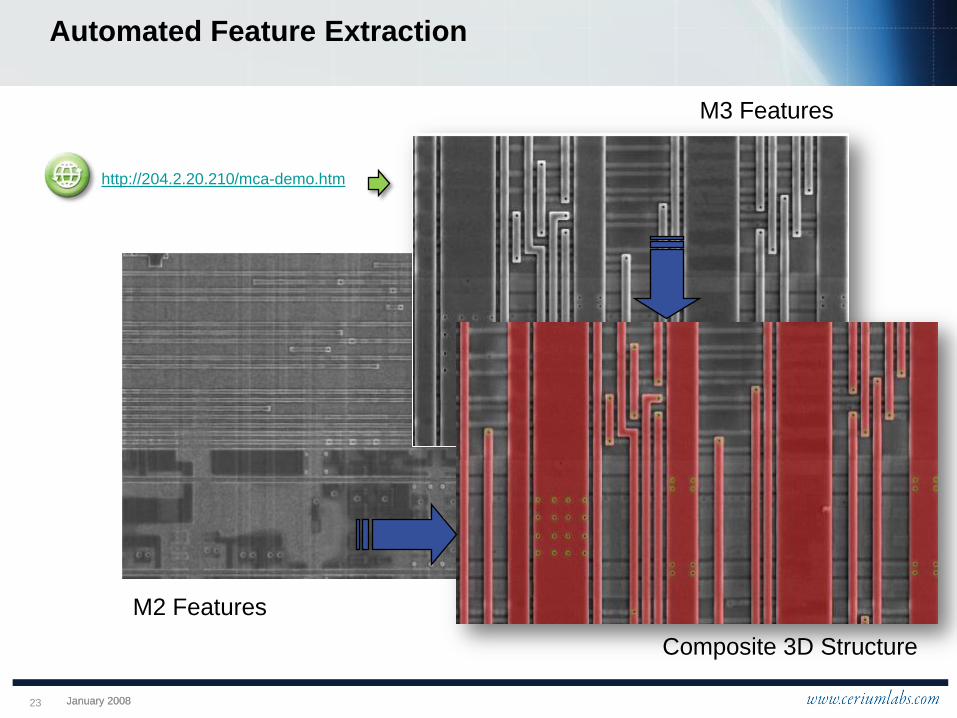
Automated Feature Extraction
M2 Features
M3 Features
Composite 3D Structure
http://204.2.20.210/mca-demo.htm

24 24
Creation of 3D models of complex interconnect structure
Combination of Optical and SEM review data into 3D models
http://204.2.20.210/M2M3/video/

25 25
Field Emission Scanning Electron Microscope
The Scanning Electron Microscope (SEM) is a microscope that uses electrons
rather than light to form an image. There are many advantages to using the SEM
instead of a light microscope. The SEM also produces images of high resolution
(8 Angstroms), which means that closely spaced features can be examined at a
high magnification. The combination of higher magnification, larger depth of
focus, greater resolution, and ease of sample observation makes the SEM a
widely used instruments in a large variety of industries.

26 26
Energy Dispersive X-Ray Spectroscopy
Used in conjunction with SEM, Energy Dispersive X-Ray Spectroscopy (EDS
or EDX) detects the elements present in a selected area of the SEM image
providing qualitative and quantitative information of material composition or
identification of contamination.

27 27
EDS elemental composition determination
Image of sample
Elemental Maps
Identified Elements
Spectral Data

28 28
Quad-SIMS
Small Area Analysis
• Small spot size at low & high
beam energies
• Checker-board data
collection for post analysis
Stability
• Uptime greater than 95%
• RSD (relative standard
deviation) of dose less than
1%

29 29
AFM
(Atomic Force Microscopy)
Typical Applications:
• Measure RMS surface
roughness of blanket films.
• Measure step heights on
patterned wafers.
AFM measures topography with a vertical precision of < 2 Å and a lateral
resolution about 50 Å.

30 30
Vapor Phase Decomposition
Sample Analysis
The sample is analyzed using a Finnigan
Element 2 High Resolution Inductively
Coupled Plasma Mass Spectrometer (HR-
ICP-MS).
The Element 2 has three separate resolution
settings, 300, 4000, and 10000, enabling the
separation of molecular ion interferences
and direct isotope interferences from the
analytes of interest.

31 31
GC-MS Identification of
Thermally Desorbed Surface Organics
SNK18 Clean Y
4.00 6.00 8.00 10.00 12.00 14.00 16.00 18.00 20.00 22.00 24.00Time0
100
%
0
100
%
WWD246 Scan EI+ TIC
4.65e614.59
13.96
11.48
4.092.55
5.984.53 13.05
22.11
17.52 18.16
23.78
WWD248 Scan EI+ TIC
4.65e6
2.56 5.98 11.49 13.04 22.11
11.48 3-heptanone13.96 azo-bis(isobutyronitrile)14.59 2-ethyl-1-hexanol22.11 di-tert-butyl-para-benzoquinone
Thermal desorption chamber designed for 300mm wafers, showing internal construction and three temperature controllers.
Chromatograms showing organic compounds desorbed from a processed wafer (red trace) and control wafer (green trace).

32 32
Neutron Activation Analysis
Cerium Labs is only one a few labs world wide that have the capability to perform ultra sensitive contamination measurements using Neutron Activation Analysis (NAA). Samples are irradiated with neutron flux from a research reactor to convert impurities into their radioactive isotopes. These isotopes decay with emission of characteristic gamma rays that are detected and analyzed using a gamma ray spectrometer.
Applications are many, but include environmental testing from coal, petroleum, and power plants. Trace contamination of pharmaceutical products.

33 33
Gas Diffusion Layer
•Analyze Gas Diffusion Layer for graphitic nature of layer
and measure SP2 character of graphite. Example: Monitor
SP2 content by measuring chemical binding information.
•Measure organic and inorganic contaminates
Platinum Catalyst Layer
•The electrode layer can be analyzed with advanced
surface science techniques.
•Image Pt aggregation and distribution with high resolution
TEM.
•Chemical composition & state information. Example:
metallic Pt and oxidized Pt can be identified.
Membrane Layer
•Identify membrane composition and moisture content of
the film through chemical and surface science techniques
•Understand membrane microstructure and changes due to
fuel cell operation with advanced imaging techniques.
Example: Loss of F from fluorinated membrane
Waste water
•Analyze contaminants in the waste water such as fluorine
and sulfur species. Trace metals such as Fe, Cr, Pt etc. can
be analyzed using high resolution chemistry techniques.
4H+
O2 H2
4e-
4e-
ANODE CATHODE
FUEL AIR
2H2O
CHARACTERIZATION PEM CELL