Embed Size (px)
Citation preview
1
Thionation of naphthalene diimide molecules: Thin-film
microstructure and transistor performance
Adam Welford,a Subashani Maniam,
b Eliot Gann,
a,c,+ Lars Thomsen,
c Steven J. Langford,
b
and Christopher R. McNeilla*
aDepartment of Materials Science and Engineering, Wellington Road, Clayton, Victoria, 3800, Australia
bSchool of Chemistry, Monash University, Wellington Road, Clayton, Victoria 3800, Australia
cAustralian Synchrotron, 800 Blackburn Road, Clayton, Victoria, 3168, Australia
*Corresponding author. E-mail: [email protected]+Present address: Materials Science and Engineering Division, National Institute of Standards and Technology,
Gaithersburg, MD 20899, USA
Keywords: OFETs, thionation, naphthalene diimides, GIWAXS, NEXAFS spectroscopy
Abstract: The replacement of the imide oxygen atoms with sulfur atoms in the naphthalene
diimide (NDI) framework is an attractive strategy for tuning of the electronic properties of
such molecules. Here we report the synthesis and characterization of the full series of six
thionated NDI molecules with branched side chains. In order to provide a direct comparison
with the unthionated parent molecule, a top-gate, bottom contact geometry is adopted, with
work function-modified gold electrodes facilitating electron injection. The highest electron
mobility was observed for the S2-cis molecule, with a mobility of 0.20 cm2/Vs compared to
0.068 cm2/Vs for the parent molecule. Mobilities slightly lower than that achieved for the S2-
cis molecule were also achieved for the S2-trans and S3 derivatives, with the S1, S4 and S2-
cis imide derivatives showing mobilities lower than the parent molecule. The thin film
microstructure of these molecules has also been explored using a combination of grazing-
incidence wide-angle X-ray scattering and near-edge X-ray absorption fine-structure
spectroscopy. The performance and microstructure of thin films deposited either by spin-
coating or blade coating are also compared.
2
1. Introduction
The development of organic semiconductors is facilitating the realization of new
technologies based on flexible devices with novel form factors produced through low-
temperature processing [1]. The ability to prepare organic field-effect transistors (OFETs) on
a variety of flexible, transparent substrates at high throughput and low cost will potentially
enable organic semiconductors to succeed in a variety of niche applications that traditional
silicon-based electronics are unsuitable for, such as radio frequency identification (RFID)
tags, flexible displays, and sensors [1,2]. Early progress in OFET research was dominated by
the development of hole transporting (or “p-type”) organic semiconductors [3] but in order to
fully develop electronic applications, electron transporting (or “n-type”) organic
semiconductors must make strides to keep pace. Progress in n-type organic semiconductor
development has been partially hampered by the difficulty of creating air stable electron
transporting materials that retain the necessary solution processability. To achieve air
stability, the lowest unoccupied molecular orbital (LUMO) level must be suitably low
(LUMO < -4.0 eV) to allow air stable charge transport within the conjugated core of the
organic semiconductor [4]. Having materials with deep LUMO levels also facilitates electron
injection from electrodes, another problem that has hampered the development of n-type
organic semiconductors [4]. The addition of strong electron withdrawing groups to the
conjugated framework has been an effective strategy to lower the LUMO levels of organic
semiconductors to realize n-type function [5]. Rylene diimide-based organic semiconductors
in particular have been an important class of n-type organic semiconductor exhibiting
relatively high electron affinities, high electron mobilities, and excellent chemical, thermal,
and photochemical stabilities [6,7]. Rylene diimides such as naphthalene diimide (NDI) and
perylene diimide (PDI) possess relatively deep LUMO levels due to the electron withdrawing
nature of the imide groups at either end of the molecule. Solubilising side chains can be
attached to the nitrogen atoms enabling solution processability. As well as being applied as
3
so-called small molecules, NDI and PDI molecules have also been widely used as acceptor
units in donor-acceptor co-polymers [3]. Both small molecule and polymeric organic
semiconductors based on NDI and PDI units have proven to be excellent materials for n-type
OFETs with mobilities of 1 to 5 cm2/Vs [8-10].
Recently, the replacement of the imide oxygen atoms with sulfur atoms in NDI and
PDI molecules has been shown to be an attractive strategy for tuning of LUMO values and
electron mobility [11-13]. Sulfur substitution is achieved by treating PDI with Lawesson’s
reagent and controlling the reaction time to tune the extent of thionation at the imide carbonyl
positions. It was reported that all the thionated PDI regioisomers could be successfully
isolated in reasonable yields except for the S2 cis-imide-PDI (which could be isolated in trace
amounts only) presumably due to unfavourable double thionation of adjacent carbonyl
positions. For PDI molecules with branched side-chains, increasing the number of sulphur
substitutions from 0 to 4 was found to increase the electron affinity from -3.67 eV to -4.12
eV, while the electron mobility was found to systematically increase with the degree of
thionation from 6.9 10-4
cm2/Vs for the unsubstituted parent molecule to 0.16 cm
2/Vs for the
S4 molecule with all four oxygen atoms replaced with sulfur atoms [11]. For NDI-based
molecules similar variation in electron affinity has been reported, both for molecules based on
branched [12] and linear [13] side-chains. Chen et al. – who reported four thionated
derivatives of NDI (S1, S2-trans, S2-cis and S3) – found that the best electron mobility was
attained for the S2-trans molecule with a value of 1.0 10-2
cm2/Vs reported [12]. The
authors however were not able to measure an electron mobility of the parent molecule likely
due to difficulties achieving electron injection. Shortly after, Kozyvz et al. reported the
properties of S1, S2-trans, S2-cis, S3 and S4 derivatives of NDI with linear side chains. While
they were not able to observe transistor action in the S4 derivative, the authors reported
4
similar mobilities of 3.9 10-2
cm2/Vs to 7.4 10
-2 cm
2/Vs for the other thionated derivatives
compared to a much lower mobility of 3.0 10-5
cm2/Vs for the parent molecule.
Here we report the synthesis and properties of the full set of 6 thionated derivatives
including the S2-cis imide derivative not previous reported. Furthermore, through the
adoption of atop-gate bottom contact geometry with work-function modified electrodes we
are able to achieve significantly higher mobilities than previously reported for the unthionated
parent molecule. Overcoming problems associated with electron injection for the parent
molecule is important in order to provide a true comparison of the charge transporting
properties of thionated vs. unthionated molecules. We also report overall higher mobilities for
the thionated NDI derivatives, with a mobility of up to 0.20 cm2/Vs achieved for the S2-cis
derivative and 0.068 cm2/Vs for the parent molecule. Finally, we also present microstructural
characterisation of films of these NDI molecules using a combination of grazing incidence
wide angle X-ray scattering (GIWAXS) and near edge X-ray absorption fine structure
(NEXAFS) spectroscopy, and compare the microstructure of spin-coated and blade-coated
samples.
2. Materials and Methods
2.1 Synthesis
The parent compound (P) was synthesised following Xiong et al. [14] Analytical thin
layer chromatography was performed on aluminium plates coated with silica gel (Silica 60
F254). Column chromatography was conducted using Merck silica gel 60, with a pore size
between 0.063 and 0.200 mm. The eluent conditions are expressed as volume-to-volume (v/v)
ratios. High-resolution electron impact mass spectrometry (HR-ESI) was performed on an
Agilent Technologies 6220 Accurate-Mass Time-of-Flight LC/MS as the solutions specified.
For mass spectrometry [M]+
denotes the molecular ion. Analyses were performed in positive
ion mode (ESI+) unless otherwise stated. Melting points were recorded on a MP50 Mettler
Toledo digital melting point apparatus at 5 oC/min.
1H and
13C nuclear magnetic resonance
5
(NMR) spectra were recorded using a Bruker DRX 400 MHz NMR spectrometer (400 MHz
for 1H NMR, 100 MHz for
13C NMR), using deuterated chloroform (CDCl3). Chemical shifts
are reported relative to the resonances of residual CHCl3 at δ = 7.26 (H) and δ = 77.2 (C). For
1H NMR spectra each resonance was assigned according to the following convention:
chemical shift () measured in parts per million (ppm), multiplicity, coupling constant, (J Hz),
number of protons and assignment. Multiplicities are denoted as (s) singlet, (d) doublet, (t)
triplet, (q) quartet, (p) pentet, or (m) multiplet and prefixed (br) broad where appropriate. The
13C NMR spectra were recorded using proton decoupled pulse sequence unless stated
otherwise. For 13
C NMR each resonance was assigned according to the following convention:
chemical shift () measured in parts per million (ppm).
A solution of Lawesson’s reagent (3.70 g, 9.15 mmol) and NDI (P) in anhydrous
toluene (40 mL) was heated at reflux for 50 h under nitrogen. The resulting brown solution
was cooled to room temperature and concentrated under vacuum to give the crude mixture
which was subjected to column chromatography (40% hexane in dichloromethane) to give the
following compounds. Each fraction was recrystallised from (50% methanol in
dichloromethane).
2,7-bis(2-ethylhexyl)-8-thioxo-7,8-dihydrobenzo[lmn][3,8]phenanthroline-1,3,6(2H)-trione,
S1. Green yellow solid (193 mg, 20%). M.p. 175-176 o
C. 1H NMR (400 MHz, CDCl3) δ 9.06
(d, J = 8.0, 1H, NDI), 8.77-8.72 (m, 2H, NDI), 8.65 (d, J = 8.0, 1H, NDI), 4.79-4.69 (m, 2H,
CH2), 4.19-4.09 (m, 2H, CH2), 2.21-2.14 (m, 1H, CH), 1.97-1.91 (m, 1H, CH), 1.43-1.24 (m,
16H, CH2), 0.96-0.85 (m, 12H, CH3). 13
C NMR (100 MHz, CDCl3) δ 193.7, 163.7, 163.6,
161.0, 136.2, 131.7, 131.1, 130.7, 130.3, 127.0, 126.8, 126.4, 125.4, 125.2, 51.0, 44.7, 38.1,
37.1, 30.9, 30.8, 28.8, 28.7, 24.2, 23.22, 23.18, 14.2, 10.9, 10.8. HRMS (TQ-MS-ESI) m/z
obsd [M+H]+ 507.2670, calcd C30H39N2O3S [M+H]
+ 507.2676.
6
2,7-bis(2-ethylhexyl)-3,6-dithioxo-2,3,6,7-tetrahydrobenzo[lmn][3,8]phenanthroline-1,8-
dione, S2-cis. Brown red solid (152 mg, 16%). M.p. 182-183 o
C. 1H NMR (400 MHz, CDCl3)
δ 8.89 (s, 2H, NDI), 8.70 (s, 2H, NDI), 4.76-4.65 (m, 4H, CH2), 2.19-2.11 (m, 2H, CH), 1.43-
1.27 (m, 16H, CH2), 0.93-0.85 (m, 12H, CH3). 13
C NMR (100 MHz, CDCl3) δ 193.7, 161.2,
135.7, 131.4, 128.9, 126.4, 125.2, 50.9, 37.1, 30.8, 28.7, 24.2, 23.2, 14.2, 10.9. HRMS (TQ-
MS-ESI) m/z obsd [M+H]+ 523.2440, calcd C30H39N2O2S2 [M+H]
+ 523.2447.
2,7-bis(2-ethylhexyl)-3,8-dithioxo-2,3,7,8-tetrahydrobenzo[lmn][3,8]phenanthroline-1,6-
dione, S2-trans. Red solid (168 mg, 18%). M.p. 181-182 o
C. 1H NMR (400 MHz, CDCl3) δ
8.98 (d, J = 8.0, 2H, NDI), 8.57 (d, J = 8.0, 2H, NDI), 4.74-4.64 (m, 4H, CH2), 2.20-2.10 (m,
2H, CH), 1.43-1.25 (m, 16H, CH2), 0.93-0.85 (m, 12H, CH3). 13
C NMR (100 MHz, CDCl3) δ
193.7, 161.2, 136.1, 131.1, 129.7, 125.4, 125.2, 51.0, 37.1, 30.8, 28.7, 24.2, 23.2, 14.2, 10.9.
HRMS (TQ-MS-ESI) m/z obsd [M+H]+ 523.2441, calcd C30H39N2O2S2 [M+H]
+ 523.2447.
2,7-bis(2-ethylhexyl)-6,8-dithioxo-7,8-dihydrobenzo[lmn][3,8]phenanthroline-1,3(2H,6H)-
dione, S2-cis imide. Orange red solid (17 mg, 2%). M.p. 181-182 o
C. 1H NMR (400 MHz,
CDCl3) δ 8.90 (d, J = 8.0, 2H, NDI), 8.58 (d, J = 8.0, 2H, NDI), 5.56-5.43 (m, 2H, CH2),
4.17-4.07 (m, 2H, CH2), 2.34-2.26 (m, 1H, CH), 1.96-1.90 (m, 1H, CH), 1.43-1.24 (m, 16H,
CH2), 0.95-0.83 (m, 12H, CH3). 13
C NMR (100 MHz, CDCl3) δ 190.8, 164.0, 137.3, 131.8,
130.6, 127.1, 124.8, 121.9, 57.63, 44.7, 38.1, 37.6, 31.7, 30.9, 30.7, 28.84, 28.81, 24.2, 24.1,
23.21, 23.19, 22.8, 14.6, 14.2, 11.2, 10.8. HRMS (TQ-MS-ESI) m/z obsd [M+H]+ 523.2441,
calcd C30H39N2O2S2 [M+H]+ 523.2447.
2,7-bis(2-ethylhexyl)-3,6,8-trithioxo-3,6,7,8-tetrahydrobenzo[lmn][3,8]phenanthrolin-1(2H)-
one, S3. Dark brown solid (85 mg, 9%). M.p. 180-181 o
C. 1H NMR (400 MHz, CDCl3) δ 8.89
(d, J = 8.0, 1H, NDI), 8.88 (d, J = 8.4, 1H, NDI), 8.77 (d, J = 8.4, 1H, NDI), 8.58 (d, J = 8.0,
7
1H, NDI), 5.55-5.42 (m, 2H, CH2), 4.76-4.65 (m, 2H, CH2), 2.34-2.28 (m, 1H, CH), 2.19-2.12
(m, 1H, CH), 1.41-1.25 (m, 16H, CH2), 0.93-0.83 (m, 12H, CH3). 13
C NMR (100 MHz,
CDCl3) δ 194.0, 161.7, 137.4, 136.8, 135.8, 131.5, 131.2, 130.6, 128.3, 125.3, 125.0, 122.0,
57.6, 50.9, 37.6, 37.1, 30.8, 30.7, 28.84, 28.75, 24.2, 24.1, 23.2, 14.2, 11.2, 10.9. HRMS (TQ-
MS-ESI) m/z obsd [M+H]+ 539.2215, calcd C30H39N2OS3 [M+H]
+ 539.2219.
2,7-bis(2-ethylhexyl)benzo[lmn][3,8]phenanthroline-1,3,6,8(2H,7H)-tetrathione, S4. Deep
purple solid (15 mg, 2%). M.p. 178-179 oC.
1H NMR (400 MHz, CDCl3) δ 8.78 (s, 4H, NDI),
5.56-5.43 (m, 4H, CH2), 2.33-2.28 (m, 2H, CH), 1.43-1.23 (m, 16H, CH2), 0.90-0.83 (m, 12H,
CH3). 13
C NMR (100 MHz, CDCl3) δ 191.2, 136.9, 130.0, 122.0, 57.6, 37.6, 32.1, 30.7, 29.9,
29.5, 28.9, 24.1, 23.2, 22.8, 14.3, 14.2, 11.2. HRMS (TQ-MS-ESI) m/z obsd [M+H]+
555.2040, calcd C30H39N2S4 [M+H]+ 555.1991.
2.2 Transistor fabrication
Top-gate bottom-contact transistors were fabricated using SiO2-coated silicon wafers
as a substrate. Gold source-drain electrodes were patterned on SiO2-coated silicon wafers via
photolithography, using AZ1518 photoresist. After patterning of the photoresist layer, 5 nm of
chromium followed by 15 nm of gold was deposited in vacuo, with the remaining resist
remove via lift-off. Wafers were diced into 12.5 mm by 12.5 mm dies, with each die
containing 16 pairs of interdigitated electrodes. Of these 16 pairs of electrodes, there were 4
pairs with a channel length of L = 2 m and 4 pairs with a channel length of L = 5 m, 4 pairs
with a channel length of L = 10 m, 4 pairs with a channel length of L = 20 m. The data
presented here are from transistors with L = 20 m. The channel width for all cases was W =
10 mm. Patterned substrates were first solvent cleaned using acetone and isopropyl alcohol in
an ultrasonic bath, followed by plasma cleaning. A thin layer of polyethylenimine ethoxylate
8
(PEIE, Sigma Aldrich) was spin coated from a 0.01 wt% 2-methoxymethanol solution (at
5000 rpm, 1 minute) and then dried on a hotplate at 110o C (10 minutes). On top of the PEIE-
treated substrates the active semiconductor layer was deposited either by spin-coating, or by
blade-coating from a home-made blade coater from hot (100 C) 10 g/L chlorobenzene
solutions. The organic semiconductor layer was annealed at 60 for 45 minutes under nitrogen.
Next, a 500 nm layer of CYTOP was spin-coated followed by the deposition of a 40 nm
aluminium gate to complete the top-gate, bottom-contact structure.
2.3 Transistor testing
Transistors were characterised in a nitrogen glove box using a Signaton H150 probe
station and Agilent B2900A 2 channel source-measure unit. Igor Pro was used to analyse the
transistor data with a script written to extract the saturation mobility and threshold voltage
from the slope of plots of (Id)½ vs. Vg according to the equation
2
2dthg
id VVV
L
WCI
where Id is the source-drain current, Vg the gate voltage, Vth the threshold voltage, Vd the
source-drain voltage, m the mobility and Ci the areal capacitance.
2.4 UV-Vis Spectroscopy
Optical absorption measurements were performed on dilute solutions in a quartz
cuvette. Spectra were measured with a PerkinElmer Lamda 950 UV/Vis/NIR Spectrometer.
2.5 Atomic Force Microscopy (AFM)
Samples were prepared on PEIE-coated silicon wafers. AFM images were acquired in
ScanAsyst mode using a Bruker Dimension Icon AFM. The Gwyddion data analysis software
was used to process and analyse the AFM images.
2.6 Grazing-incidence wide-angle X-ray scattering
GIWAXS measurements were conducted at the SAXS/WAXS beamline of the
Australian Synchrotron [15]. Thin films were prepared on Si\SiO2\PEIE substrates following
9
the same protocol as employed for transistors. Highly collimated 9 keV X-ray photons were
aligned parallel to the substrates by varying sample height and polar angle while measuring
the transmitted signal with a crystal analyser. 2D GIWAXS patterns were recorded on a
Dectris Pilatus 1M detector with each 2D scattering pattern being the result of a total of 3 s of
exposure. Three 1 s exposures were taken at different lateral detector positions to fill in the
gaps between modules in the detector, and combined in software. Angular steps of 0.01° were
taken near the critical angle, which was determined as the angle of maximum scattered
intensity. The sample to detector distance was measured using a silver behenate scattering
standard. A modified version of the NIKA small angle scattering analysis package [16] was
used to analyse the data, with peak fitting performed using least squares multipeak fitting
within IgorPro.
2.7 Near-edge X-ray absorption Fine-structure Spectroscopy
NEXAFS spectra were collected at the Soft X-ray beamline of the Australian
Synchrotron [17]. The recorded signal was normalized to the incident photon flux using the
‘‘stable monitor method,’’ where a gold mesh is used to track variations in X-ray flux during
data acquisition with carbon contamination on the gold mesh calibrated by measuring the
direct signal with a silicon photodiode [18]. The normalized spectra were scaled by
subtracting a background, which scales according to the atomic scattering factors of the
material before the onset of the first feature setting, i.e. the absorption measured at 280 eV,
and then normalizing to the value of 1 at 320 eV. Average tilt angles were determined by
measuring angle-dependent NEXAFS spectra and fitting to the expression:
)]1cos3)(1cos3(1[ 22
2
1
3
1 I
where I is the resonant intensity, is the X-ray incidence angle and is the average tilt angle
of the C 1s to π* transition dipole moment (TDM) [19]. Data were analysed with the
assistance of the QANT software [20].
10
3. Results
3.1. General Materials Properties
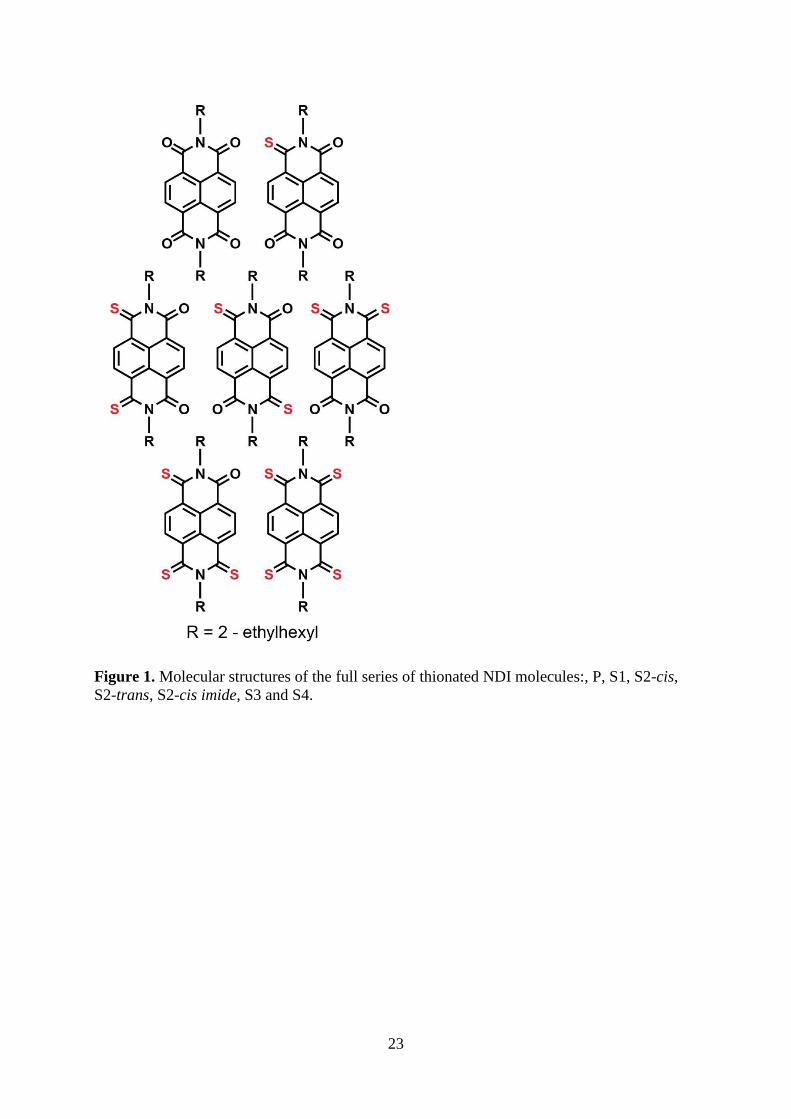
Figure 1 shows the chemical structures of the full series of thionated NDI molecules.
Thionation alters the generic framework itself rather than adding pendant electron
withdrawing units. Sulfur – as compared to oxygen – is slightly larger in size but similarly
charged and is thus correspondingly less electronegative which alters the effect it has on the
conjugated naphthalene core. As seen in Figure 1, partial substitution breaks the symmetry of
the NDI framework, with the S1 and S3 derivatives losing all symmetry. Each of the S2
derivatives retains a separate degree of molecular symmetry, while the full 3-fold symmetry
of the NDI framework is restored in the S4 derivative.
Cyclic voltammetry has been used to measure the electron affinity (LUMO energy)
and ionisation potential (HOMO) of the thionated NDI series, see Table 1. Similar to previous
reports, thionation leads to a lowering of the LUMO, which decreases from -3.67 eV for the
parent molecule to -4.25 eV for the S4 derivative. Interestingly the S2-cis imide derivative
exhibits a LUMO of -4.01 eV which is intermediate to that of the S2-cis and S2-imide
derivatives. There is also a systematic increase in the HOMO level with thionation which
increases from -6.94 for the parent molecule to -6.59 for the S4 derivative. These changes in
HOMO and LUMO values with thionation result in a narrowing of the electronic bandgap
from 3.27 eV for the parent molecule to 2.34 for S4.
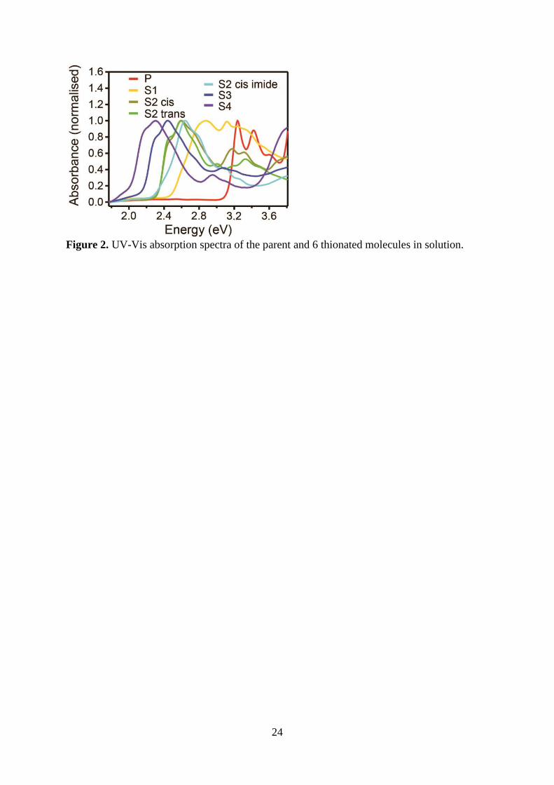
The UV-Vis absorption spectra of the thionated NDI series in chlorobenzene are
presented in Figure 2. In accordance with the changes in HOMO and LUMO values, there is a
systematic decrease in the onset of absorption from the UV for the parent molecule to the red
for S4. The biggest shift in absorption onset is seen going from the parent molecule to S1,
with the absorption onset changing from ~ 3.0 eV to ~ 2.45 eV. Further thionation to S2
results in a shift in the absorption onset by only ~ 0.1 eV to ~ 2.35 eV. While the three S2
derivatives have similar absorption onsets, the spectrum of the S2-cis imide molecule shows
11
distinct features to those of the S2-cis and S2-imide derivatives which both have quite similar
absorption spectra in the visible range. In particular the lowest energy absorption peak at 2.4
eV appears suppressed in the spectrum of S2-cis imide, with the second absorption peak also
blue-shifted relative to that of the other S2 derivatives. Thionation to S3 and S4 continues the
trend of decreasing absorption onsets, with values of ~ 2.15 eV and 2.0 eV for S3 and S4
respectively.
3.2. Transistor Data
Top-gate bottom-contact (TGBC) OFET devices were fabricated to examine the
changes to the transport properties of the molecules with thionation. As the thionated NDI
derivatives are n-type electron transporting materials, difficulty with the injection of electrons
from gold electrodes into the molecules can be problematic due to the large difference
between the work function of gold and the LUMO of n-type materials. To minimise this
difference, here the work function of the gold electrodes was modified via the application of a
thin polyethylenimine ethoxylated (PEIE) layer [21]. Zhou et al. have shown that the use of
PEIE can decrease the work function of gold by over 1 eV from 5.10 eV for untreated gold to
3.90 eV for gold with PEIE-treatment [21]. Furthermore, previous studies have shown that
PEIE-treated electrodes are effective in enabling n-channel operation in top-gate transistors by
facilitating electron injection [21,22].
Thin films of the parent molecule or the thionated NDI derivatives were coated on top
of PEIE-treated gold electrodes either by spin coating or blade coating from hot (100 C) 10
g/L chlorobenzene solutions. Subsequently the organic semiconductor layer was annealed at
60 C for 45 minutes under nitrogen. Next, a 500 nm layer of CYTOP was spin-coated
followed by the deposition of a 40 nm aluminium gate to complete the top-gate bottom-
contact structure. Full details of the device fabrication procedure can be found in the materials
and methods section.
12
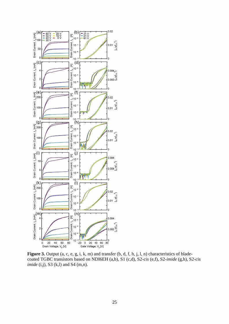
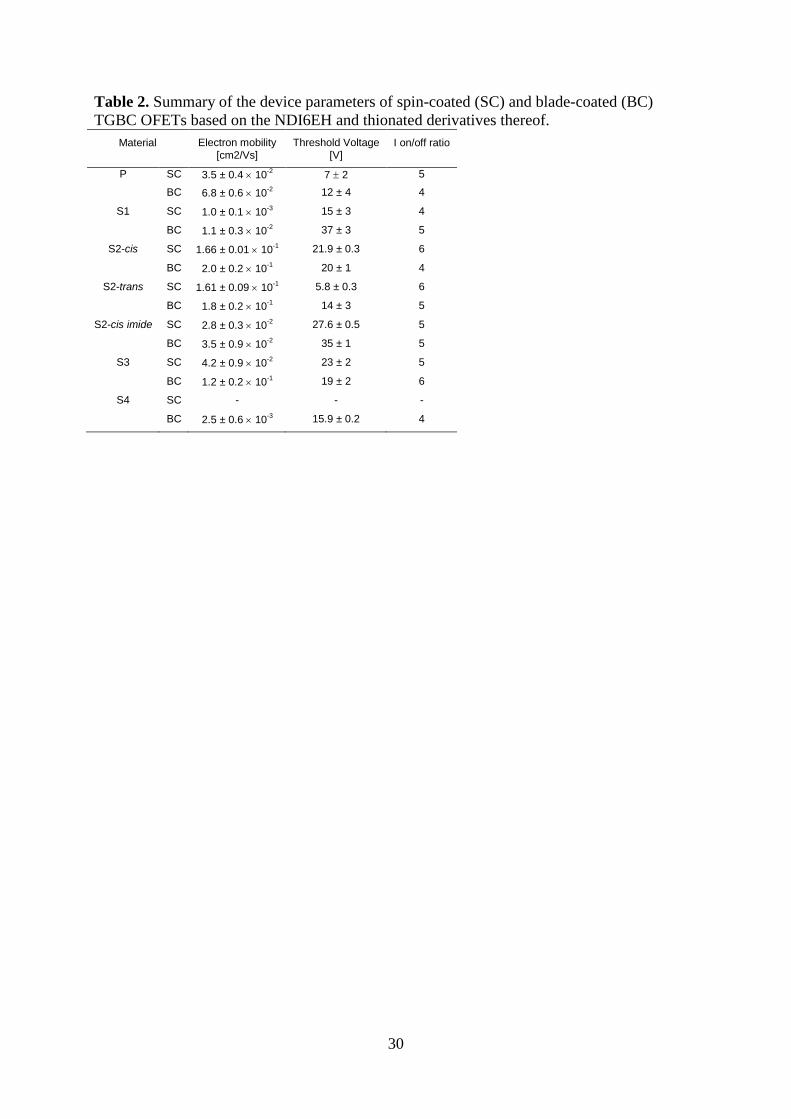
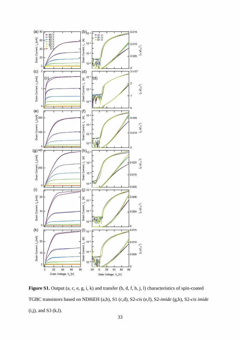
Figure 3 shows representative output and transfer characteristics of transistors
fabricated via blade-coating of the semiconducting layer. Blade-coated devices exhibited
consistently higher mobilities than spin-coated devices, with output and transfer
characteristics of spin-coated devices provided in Figure S1 (supporting information). Table 2
summarizes the device parameters of both spin-coated and blade-coated OFETs. The electron
mobility of each device was calculated from the saturated regime of the transfer curves. Along
with the mobility values, the threshold voltages and current on/off ratios are also summarized
in Table 2. As seen in Figure 3 (a,b), OFETs based on the parent molecule show reliable n-
type transistor behavior, attributed to the ease of injecting electron from the PEIE-treated Au
electrodes. The transfer curves show a clear square-root dependence of saturation current on
gate voltage enabling a robust determination of electron mobility. Compared to the other
reports on the effect of thionation on NDI molecules where the parent molecule either
exhibited no n-channel transistor behavior [12] or a very low electron mobility of 3.0 10-5
cm2/Vs, [13] we were able to achieve average electron mobilities of 3.5 10
-2 cm
2/Vs for
spin-coated transistors and 6.8 10-2
cm2/Vs for blade coated transistors based on the parent
molecule. These values are slightly lower than the best-reported mobility values for solution-
processed NDI transistors of ~ 0.2 cm2/Vs, [23,24] however this is likely to be due to the use
of different side chains in these other studies. Thus by solving the problem of electron
injection in solution-processed films of the parent molecule we have been able to reliably
characterise the electron transporting properties of the unthionated molecule which is a
necessary base value when assessing the effect of thionation on electron mobility. The curves
in Figure 3 show both forward and reverse voltage scans with some hysteresis evident.
Hysteresis is more prominent in the blade-coated devices, with the spin-coated devices
exhibited much cleaner characteristics in general (see Figure S1).
13
Comparing the mobility values of the thionated derivates with that of the parent
molecule, thionation does not always result in an improvement in mobility. For the S1
derivative, the electron mobility is found to decrease to 1.1 10-2
cm2/Vs for blade coated
films compared to 6.8 10-2
cm2/Vs for the parent molecule. For the S2-cis and S2-trans and
S3 molecules, however an improvement in electron mobility is seen, increasing to 0.12 – 0.20
cm2/Vs. For the S2-cis imide molecule, a mobility slightly lower than that of the parent
molecule is measured (3.5 10-2
cm2/Vs) indicating that the charge transporting properties of
the S2 derivatives are sensitive to which oxygen atoms are replaced with sulfur atoms. The
poor film forming properties of the S4 derivative hindered the fabrication of S4 OFETs.
Transistor action not achieved in spin-coated films, with a low mobility of only 2.5 ± 0.6
10-3
cm2/Vs achieved for blade-coated devices. Thus out of the 6 thionated derivates only 3
derivatives (the S2-cis, S2-trans and S3 derivatives) outperformed the parent molecule. This
improved mobility however was significant with respect to the parent molecule, achieving
values of ~ 0.2 cm2/Vs which are also significantly higher than those reported previously
[12,13].
Looking at the other transistor parameters, OFETs based on the thionated molecules
tend to have higher threshold voltages than OFETs based on the parent molecule, with
threshold voltages as high as 37 V for blade-coated S1 OFETs compared to values of 7 V
(spin-coated) and 12 V (blade-coated) for OFETs based on the parent molecule. The S2-trans
transistors show relatively low threshold values of 6 – 14 V comparable with those of the
parent molecule indicating that higher threshold values are not always exhibited by OFETs
based on thionated molecules. The differences in threshold voltage may be related to
differences in film morphology which is examined below. Good on/off ratios are also
exhibited by the transistors, up to 106 though with some values as low as 10
4 depending on the
nature of device preparation (i.e. spin-coated vs. blade coated).
14
3.3.Thin Film Microstructure
3.3.1. Atomic Force Microscopy
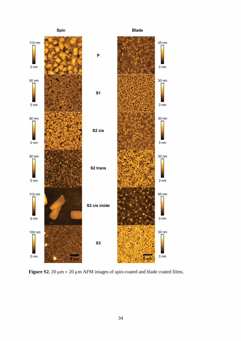
Thin films prepared in the same manner as OFETs (i.e. on PEIE-coated substrates)
were imaged via atomic force microscopy. Figure 4 presents 5 5 m images of both spin-
coated and blade-coated films (20 20 m images can be found in the Supporting
Information, Figure S2). While all samples were prepared in the same fashion (i.e. with the
same spin-coating or blade-coating parameters) the different molecules exhibit different thin
film morphologies. Differences are also seen in general between the morphologies of spin-
coated and blade-coated films. Looking at the spin-coated samples, the parent molecule is
found to produce relatively large, tall islands whereas the spin-coated films of most thionated
samples are characterised by smaller, shorter islands. Spin-coated films of S1 and S3 tend to
produce elongated domains compared to the more rounded domains of spin-coated parent and
S2-cis films. The spin-coated S2-trans and S2-cis imide films exhibit more platelet like
structures, with the size of the platelets in the S2-cis imide film being especially large (of the
order of the imaging window) and the platelets in the S2-trans film rather high. The S4
surface shows the lowest, smallest island formations interspersed with larger sharp-ridged
circular islands suggestive of dewetting and poor surface coverage. It might be seen as
surprising that despite these rather rough morphologies exhibited by spin-coated films that
appreciable charge transport mobilities have been achieved in the top-gate OFETs reported
here; indeed the mobilities reported here are higher than those achieved in bottom-gate
OFETs reported elsewhere [12,13]. However the domains imaged with AFM in the spin-
coated samples are clearly interconnected as evidenced by the transistor data.
Looking at the blade-coated samples, more consistent morphologies across the
different molecules are observed as compared to the spin-coated samples. Compared to the
spin-coated films, larger-sized domains are observed in general in the blade-coated films with
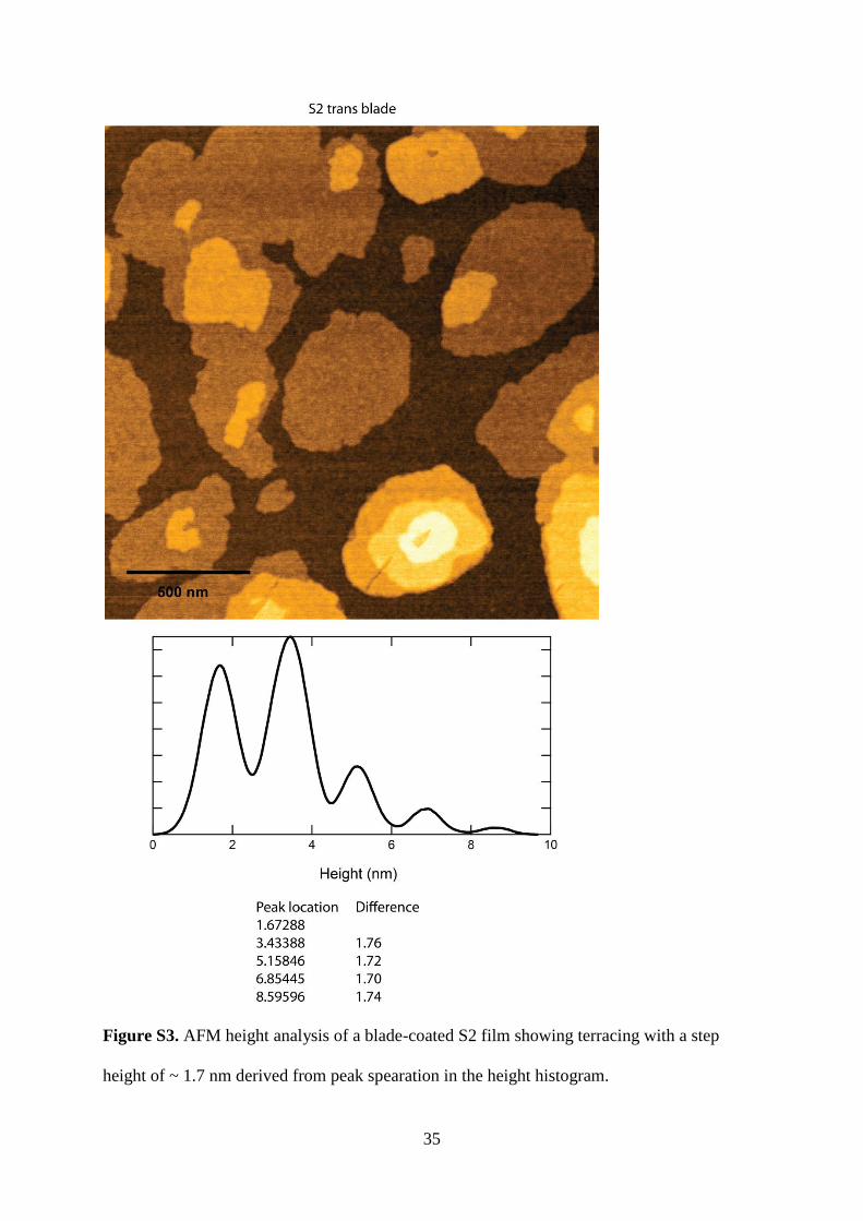
lower film roughness. Especially interesting is the fact that terracing can be clearly seen in
15
most blade-coated samples with the step-height of these terraces (~ 1.7 nm) consistent with
single-molecule steps (see Figure S3 in the supporting information). The S3 and S4 films
appear the most different out of the blade-coated films with S3 films exhibiting less-clear
terracing and some cracks in the film, and S4 again showing poor surface coverage. The
enhanced electron mobility of the blade-coated films is likely associated with the improved
morphology (lower roughness, increased molecular order) compared to spin-coated films.
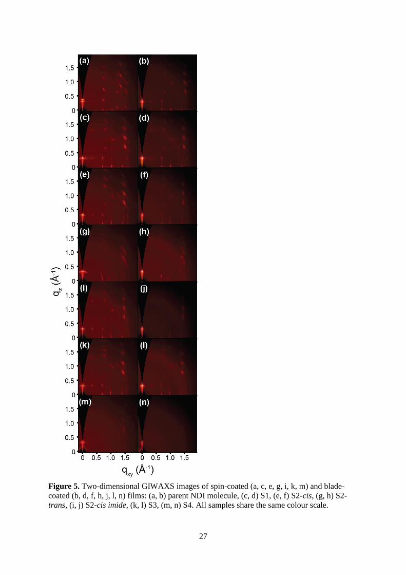
3.3.2. GIWAXS
The thin-film microstructure of spin-coated and blade-coated films has been studied
with grazing incidence wide-angle X-ray scattering (GIWAXS). Figure 5 shows the two-
dimensional X-ray scattering patterns of spin-coated and blade-coated samples. When
comparing spin-coated and blade-coated films, the same diffraction features are in general
observed but with a greater radial distribution (or ‘arcing’) of peaks in the spin-coated films
reflecting a higher degree of out-of-plain mosaicity. This greater mosaicity of the spin-coated
samples is in agreement with the AFM morphology analysis which shows the spin-coated
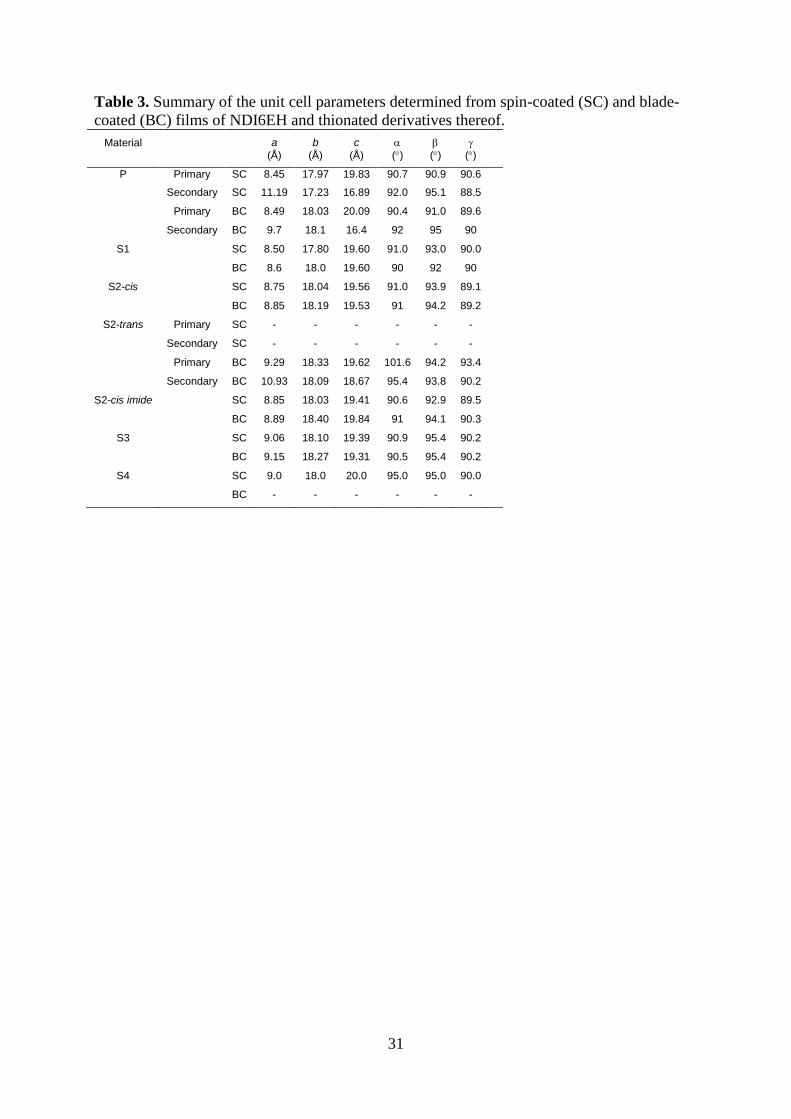
samples to be rougher with more angular features. Table 3 summarises the calculated unit cell
parameters, with most molecules generally having unit cells close to orthorhombic; for the
case of monoclinic and triclinic cells the unit cell angles are typically still close to 90. Note
that precise unit cell values could not be determined for the spin-coated S2-trans sample due
to the degree of disorder in the GIWAXS image. All scattering patterns are consistent with the
molecules standing ‘edge-on’ to the substrate. The intense peak observed along qz indexed as
the (001) reflection corresponds to the separation of planes of molecules separated by the
alkyl side chains, with a spacing of the c-axis of ~ 19.5 to 20.0 Å observed, roughly consistent
with the step height measured by AFM. The length of a stretched out molecule is ~ 23.5 Å
[12] indicating titling of the molecule within the unit cell, as confirmed by NEXAFS
spectroscopy (vide infra). Most molecules exhibit similar unit cell angles close to 90 with
values of the a-, b-, and c-axes of ~ 18 Å, 9 Å, and 19.5 Å respectively. The values for the a-
16
and b-axes are roughly twice as large as those found for NDI molecules with linear side
chains [13,25] suggesting a more complex packing with more than one molecule per unit cell.
Interestingly the GIWAXS patterns of the parent NDI molecule is described by two unit cells
likely due to the presence of two polymorphs observed in both spin-coated and blade-coated
films. The secondary unit cell has a much lower c-axis dimension of ~ 16.5 Å compared to ~
20 Å for the primary unit cell. The primary unit cell dominates in the blade-coated sample
with the secondary unit cell more prominent in the spin-cast sample. The S2-trans sample also
exhibits two polymorphs however the differences between these two polymorphs are more
subtle. Across the other molecules the unit cell dimensions and angles are quite similar
indicating that thionation does not have a significant impact on the broad crystal packing. The
S2-trans is the most different, with the largest titling of the unit cell ( = 101.6 for the
primary unit cell) of all the molecules.
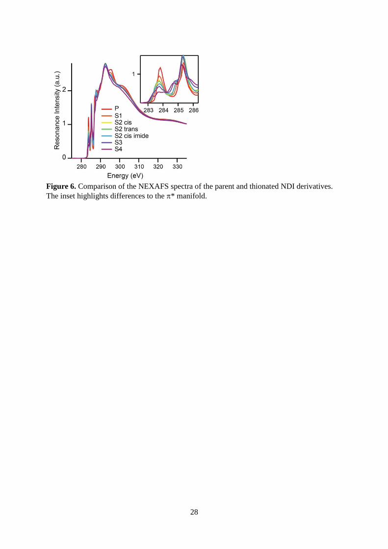
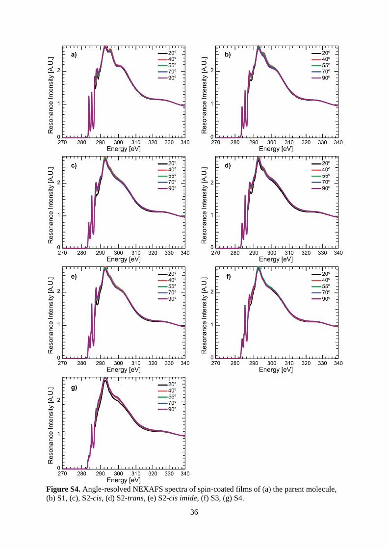
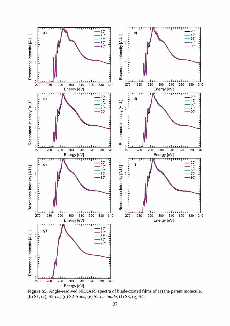
2.3.3.NEXAFS Spectroscopy
Complimentary to GIWAXS, NEXAFS spectroscopy provides information about the
molecular orientation of the conjugated core and spectroscopic information about the
unoccupied density of states. From angle-dependent NEXAFS spectra acquired with X-ray
angle of incidence varying from glancing (20) to normal (90), the orientation of different
molecular orbitals with respect to the substrate (more precisely, the orientation of the
associated transition dipole moment) can be determined. Angle dependent Carbon K-edge
NEXAFS spectra for spin-coated and blade-coated samples are shown in Figures S4 and S5 in
the supporting information. In all cases, little or no dichroism is seen at energies associated
with transitions from 1s to * orbitals indicating an average tilt angle of ~ 55 for the C 1s
* transition dipole moment from the surface normal. While such an angle could be seen as
reflecting a random molecular orientation, the highly-ordered morphologies of blade coated
samples and the GIWAXS data indicate a preferential orientation of the unit cell. Hence the
17
NEXAFS data provides evidence that the conjugated core of all molecules adopts a
preferential orientation with the planar conjugated core subtending an angle of ~ 55 from the
substrate plane. Such an end-on orientation of the conjugated backbone (rather than lying flat)
is consistent with the step height of the terraces measured by AFM.
While the GIWAXS and AFM analysis yield a range of unit cells and surface
morphologies, the consistency of the tilting of the conjugated core is likely a result of the
common branched side chain, with recent studies showing that the side chain playing a
dominant role in determining molecular orientation [26]. Although NEXAFS spectroscopy
does not reveal differences in molecular orientation, it does reveal significant differences in
the near-edge fine structure with thionation, see Figure 6. Figure 6 compares the NEXAFS
spectra of the different molecules taken with an angle of incidence of 55. Thionation leads to
pronounced changes in the * manifold as highlighted by the inset of Figure 6. These peaks
between 283 eV and 286 eV correspond to transitions between the 1s and * antibonding
orbitals, with the differences seen reflecting differences in the unoccupied electronic density
of states. (The UV-Vis data in contrast represent a convolution of the occupied and
unoccupied density of states.) The spectrum of the parent molecule shows a peak at ~ 283.8
eV which is associated with the LUMO and two peaks at 285 eV and 285.5 eV associated
with the LUMO +1 and LUMO +2 [27]. With thionation a systematic shift in the onset of X-
ray absorption is seen consistent with a lowering of the LUMO energy. Thionation also results
in a broadening of the electronic structure between 283 and 284 eV. While the structure of the
LUMO +1 peak is similarly affected by thionation, the LUMO +2 appears to be relatively
insensitive to thionation. Interestingly a peak at 286 eV also emerges with thionation.
Curiously for the S4 and parent molecules which have the same symmetry, the S4 molecule
exhibits a more complicated electronic structure.
18
4. Discussion
In contrast to previous studies, [12,13] our results show that thionation does not
always result in improved charge transport with respect to the unthionated parent molecule. In
these previous studies charge transport was likely limited by charge injection, with the lower
electron affinity of the unthionated molecule presenting a large injection barrier for electrons
from gold. By using PEIE-modified gold electrodes we have been able to achieve good
electron injection and relatively high mobilities for the parent molecule, of the order of 0.07
cm2/Vs. The S2-cis and S2-trans derivatives exhibited the highest mobilities, around 0.2
cm2/Vs representing a significant improvement compared to the parent molecule. The S1, S2-
cis imide and S4 derivatives however did not result in higher mobilities than the parent
molecule. So while this study confirms the previous studies that thionation can lead to an
improvement in charge transport properties, thionation does not always yield an improvement
with the charge transport performance sensitive to the nature and degree of thionation. For the
case of the S2-cis imide molecule which has not been reported before, it has a significantly
lower mobility of ~ 0.03 cm2/Vs compared to the other S2 derivatives. This is interesting as it
shows that transport performance is not simply sensitive to the degree of thionation. The
lower performance of the S2-cis imide derivative is not easily explained by its microstructure,
with AFM analysis showing large domains in spin-coated films, and flat, terraced films in
blade-coated films. Indeed, the GIWAXS analysis shows that the spin-coated S2-cis imide
films have low mosaicity and a single polymorph, both of which should be favorable for
charge transport. Indeed, the S2-trans derivative appears to exhibit two polymorphs but none-
the-less exhibits relatively high charge transport mobilities. From the unit cell parameters
determined from GIWAXS there is no clear tell-tale sign that would explain the observed
differences in mobility, with the S1 and S2-cis derivatives having very similar unit cell
dimensions but mobilities differing by a factor of 100 (0.001 cm2/Vs for S1 and 0.2 cm
2/Vs
for S2-cis). The ultimate explanation for the observed variations in mobility is likely due to in
19
the details of the electronic structure of these molecules and the exact modes of packing.
Although similar unit cell dimensions are evidenced, subtle variations in the packing and
relative placement of molecules within the unit cell may lead to different charge transfer
integrals and hence charge carrier mobilities. NEXAFS spectroscopy reveals clear differences
in the electronic structure of the molecules which shows that thionation can affect significant
changes in electronic structure while minimizing the changes to the chemical structure and
film microstructure. Further investigations into the packing of the molecules within the unit
cell, and theoretical modeling of the NEXAFS spectra (both beyond the scope of this work)
will help to elucidate the variations in molecular packing and electronic structure afforded by
thionation.
5. Conclusions
We have reported the synthesis and characterization of the full series of six thionated
NDI molecules for OFET applications. Through device engineering, problems associated with
charge injection have been overcome enabling a proper evaluation of the effect of thionation
on charge transport. Of the six different thionated derivatives investigated, only the S2-cis (
= 0.2 cm2/Vs), S2-trans ( = 0.18 cm
2/Vs), and S3 ( = 0.12 cm
2/Vs) molecules showed
higher charge transport mobilities than the unthionated parent molecule ( = 0.068 cm2/Vs).
The thin-film microstructure of both spin-coated and blade-coated films has been investigated
with AFM, GIWAXS and NEXAFS spectroscopy. Blade-coated films exhibit a higher degree
of order with AFM revealing molecular terracing and lower roughness, and GIWAXS
showing a lower degree of mosaicity in blade-coated samples. The improved order in blade-
coated samples explains the higher charge transport properties observed in general for blade-
coated OFETs. NEXAFS spectroscopy revealed a similar tilting of all molecules, with
pronounced differences in the * electronic structure observed between samples. Comparing
the microstructures of the different derivatives, no clear microstructural sign is seen that
20
explains the mobilities. Instead, thionation is likely producing subtle differences in molecular
packing and electronic structure, leading to tuning of charge transport properties.
Acknowledgements
Part of this research was performed at soft X-ray and SAXS/WAXS beamlines at Australian
Synchrotron, part of ANSTO. This work was also performed in part at the Melbourne Centre
for Nanofabrication (MCN) in the Victorian Node of the Australian National Fabrication
Facility (ANFF). Financial support from the Australian Research Council through the
Discovery Grant Scheme (DP130101861 and DP170104477) is gratefully acknowledged.
21
References
[1] K.-J. Baeg, M. Caironi, Y.-Y. Noh, Toward Printed Integrated Circuits based on
Unipolar or Ambipolar Polymer Semiconductors, Adv. Mater. 25 (2013) 4210-44.
[2] C.-a. Di, F. Zhang, D. Zhu, Multi-Functional Integration of Organic Field-Effect
Transistors (OFETs): Advances and Perspectives, Adv. Mater. 25 (2013) 313-30.
[3] A. Facchetti, π-Conjugated Polymers for Organic Electronics and Photovoltaic Cell
Applications, Chem. Mater. 23 (2011) 733-58.
[4] Y. Zhao, Y. Guo, Y. Liu, 25th Anniversary Article: Recent Advances in n-Type and
Ambipolar Organic Field-Effect Transistors, Adv. Mater. 25 (2013) 5372-91.
[5] J.E. Anthony, A. Facchetti, M. Heeney, S.R. Marder, X. Zhan, n-Type Organic
Semiconductors in Organic Electronics, Adv. Mater. 22 (2010) 3876-92.
[6] X. Zhan, A. Facchetti, S. Barlow, T.J. Marks, M.A. Ratner, M.R. Wasielewski, S.R.
Marder, Rylene and Related Diimides for Organic Electronics, Adv. Mater. 23 (2011)
268-84.
[7] F. Wurthner, M. Stolte, Naphthalene and perylene diimides for organic transistors,
Chem. Comm. 47 (2011) 5109-15.
[8] F. Zhang, Y. Hu, T. Schuettfort, C.-a. Di, X. Gao, C.R. McNeill, L. Thomsen, S.C.B.
Mannsfeld, W. Yuan, H. Sirringhaus, D. Zhu, Critical Role of Alkyl Chain Branching
of Organic Semiconductors in Enabling Solution-Processed N-Channel Organic Thin-
Film Transistors with Mobility of up to 3.50 cm2 V–1 s–1, J. Am. Chem. Soc. 135
(2013) 2338-49.
[9] S. Bucella, A. Luzio, E. Gann, L. Thomsen, C.R. McNeill, G. Pace, A. Perinot, Z.
Chen, A. Facchetti, M. Caironi, Macroscopic and high-throughput printing of aligned
nanostructured polymer semiconductors for MHz large-area electronics, Nat Commun
6 (2015) 8394.
[10] S. Tatemichi, M. Ichikawa, T. Koyama, Y. Taniguchi, High mobility n-type thin-film
transistors based on N,N′-ditridecyl perylene diimide with thermal treatments, Appl.
Phys. Lett. 89 (2006) 112108.
[11] A.J. Tilley, C. Guo, M.B. Miltenburg, T.B. Schon, H. Yan, Y. Li, D.S. Seferos,
Thionation Enhances the Electron Mobility of Perylene Diimide for High Performance
n-Channel Organic Field Effect Transistors, Adv. Funct. Mater. 25 (2015) 3321-29.
[12] W. Chen, J. Zhang, G. Long, Y. Liu, Q. Zhang, From non-detectable to decent:
replacement of oxygen with sulfur in naphthalene diimide boosts electron transport in
organic thin-film transistors (OTFT), J. Mater. Chem. C 3 (2015) 8219-24.
[13] L.M. Kozycz, C. Guo, J.G. Manion, A.J. Tilley, A.J. Lough, Y. Li, D.S. Seferos,
Enhanced electron mobility in crystalline thionated naphthalene diimides, J. Mater.
Chem. C 3 (2015) 11505-15.
[14] K. Xiong, Y. Xiao, Synthesis of tetraalkyl naphthalene bisanhydride and its model
condensations with amines, Tetrahedron Lett. 54 (2013) 3171-75.
[15] N.M. Kirby, S.T. Mudie, A.M. Hawley, D.J. Cookson, H.D.T. Mertens, N. Cowieson,
V. Samardzic-Boban, A low-background-intensity focusing small-angle X-ray
scattering undulator beamline, J. Appl. Cryst. 46 (2013) 1670-80.
[16] I. Ilavsky, Nika - software for 2D data reduction, J. Appl. Cryst. 45 (2012) 324-28.
[17] B.C.C. Cowie, A. Tadich, L. Thomsen, The Current Performance of the Wide Range
(90--2500 eV) Soft X-ray Beamline at the Australian Synchrotron, AIP Conf. Proc.
1234 (2010) 307-10.
[18] B. Watts, L. Thomsen, P.C. Dastoor, Methods in carbon K-edge NEXAFS:
Experiment and analysis, J. Elec. Spec. & Rel. Phen. 151 (2006) 105-20.
[19] J. Stöhr, NEXAFS Spectroscopy, Springer, Berlin, 1992.
22
[20] E. Gann, C.R. McNeill, A. Tadich, B.C.C. Cowie, L. Thomsen, Quick AS NEXAFS
Tool (QANT): A program for NEXAFS loading and analysis developed at the
Australian Synchrotron, J. Synchrotron Rad. 23 (2016) 374-80.
[21] Y. Zhou, C. Fuentes-Hernandez, J. Shim, J. Meyer, A.J. Giordano, H. Li, P. Winget,
T. Papadopoulos, H. Cheun, J. Kim, M. Fenoll, A. Dindar, W. Haske, E. Najafabadi,
T.M. Khan, H. Sojoudi, S. Barlow, S. Graham, J.-L. Brédas, S.R. Marder, A. Kahn, B.
Kippelen, A Universal Method to Produce Low–Work Function Electrodes for
Organic Electronics, Science 336 (2012) 327-32.
[22] M.M. Nahid, R. Matsidik, A. Welford, E. Gann, L. Thomsen, M. Sommer, C.R.
McNeill, Unconventional Molecular Weight Dependence of Charge Transport in the
High Mobility n-type Semiconducting Polymer P(NDI2OD-T2), Adv. Funct. Mater.
(2017) DOI:10.1002/adfm.201604744.
[23] I. Tszydel, M. Kucinska, T. Marszalek, R. Rybakiewicz, A. Nosal, J. Jung, M.
Gazicki-Lipman, C. Pitsalidis, C. Gravalidis, S. Logothetidis, M. Zagorska, J. Ulanski,
High-Mobility and Low Turn-On Voltage n-Channel OTFTs Based on a Solution-
Processable Derivative of Naphthalene Bisimide, Adv. Funct. Mater. 22 (2012) 3840-
44.
[24] M. Ichikawa, Y. Yokota, H.-G. Jeon, G.d.R. Banoukepa, N. Hirata, N. Oguma,
Comparative study of soluble naphthalene diimide derivatives bearing long alkyl
chains as n-type organic thin-film transistor materials, Org. Electron. 14 (2013) 516-
22.
[25] D. Shukla, S.F. Nelson, D.C. Freeman, M. Rajeswaran, W.G. Ahearn, D.M. Meyer,
J.T. Carey, Thin-Film Morphology Control in Naphthalene-Diimide-Based
Semiconductors: High Mobility n-Type Semiconductor for Organic Thin-Film
Transistors, Chem. Mater. 20 (2008) 7486-91.
[26] C. Zhang, D. Yuan, H. Wu, E. Gann, L. Thomsen, C.R. McNeill, C.-a. Di, X. Zhu, D.
Zhu, Insight into thin-film stacking modes of [small pi]-expanded quinoidal molecules
on charge transport property via side-chain engineering, J. Mater. Chem. C 5 (2017)
1935-43.
[27] M. Ruiz-Osés, T. Kampen, N. González-Lakunza, I. Silanes, P.M. Schmidt-Weber, A.
Gourdon, A. Arnau, K. Horn, J.E. Ortega, Spectroscopic Fingerprints of Amine and
Imide Functional Groups in Self-Assembled Monolayers, ChemPhysChem 8 (2007)
1722-26.
23
Figure 1. Molecular structures of the full series of thionated NDI molecules:, P, S1, S2-cis,
S2-trans, S2-cis imide, S3 and S4.
24
Figure 2. UV-Vis absorption spectra of the parent and 6 thionated molecules in solution.
25
Figure 3. Output (a, c, e, g, i, k, m) and transfer (b, d, f, h, j, l, n) characteristics of blade-
coated TGBC transistors based on NDI6EH (a,b), S1 (c,d), S2-cis (e,f), S2-imide (g,h), S2-cis
imide (i,j), S3 (k,l) and S4 (m,n).
26
Figure 4. Surface topography of spin-coated (a, c, e, g, i, k, m) and blade-coated (b, d, f, h, j,
l, n) films: (a, b) parent NDI molecule, (c, d) S1, (e, f) S2-cis, (g, h) S2-trans, (i, j) S2-cis
imide, (k, l) S3, (m, n) S4.
27
Figure 5. Two-dimensional GIWAXS images of spin-coated (a, c, e, g, i, k, m) and blade-
coated (b, d, f, h, j, l, n) films: (a, b) parent NDI molecule, (c, d) S1, (e, f) S2-cis, (g, h) S2-
trans, (i, j) S2-cis imide, (k, l) S3, (m, n) S4. All samples share the same colour scale.
28
Figure 6. Comparison of the NEXAFS spectra of the parent and thionated NDI derivatives.
The inset highlights differences to the * manifold.
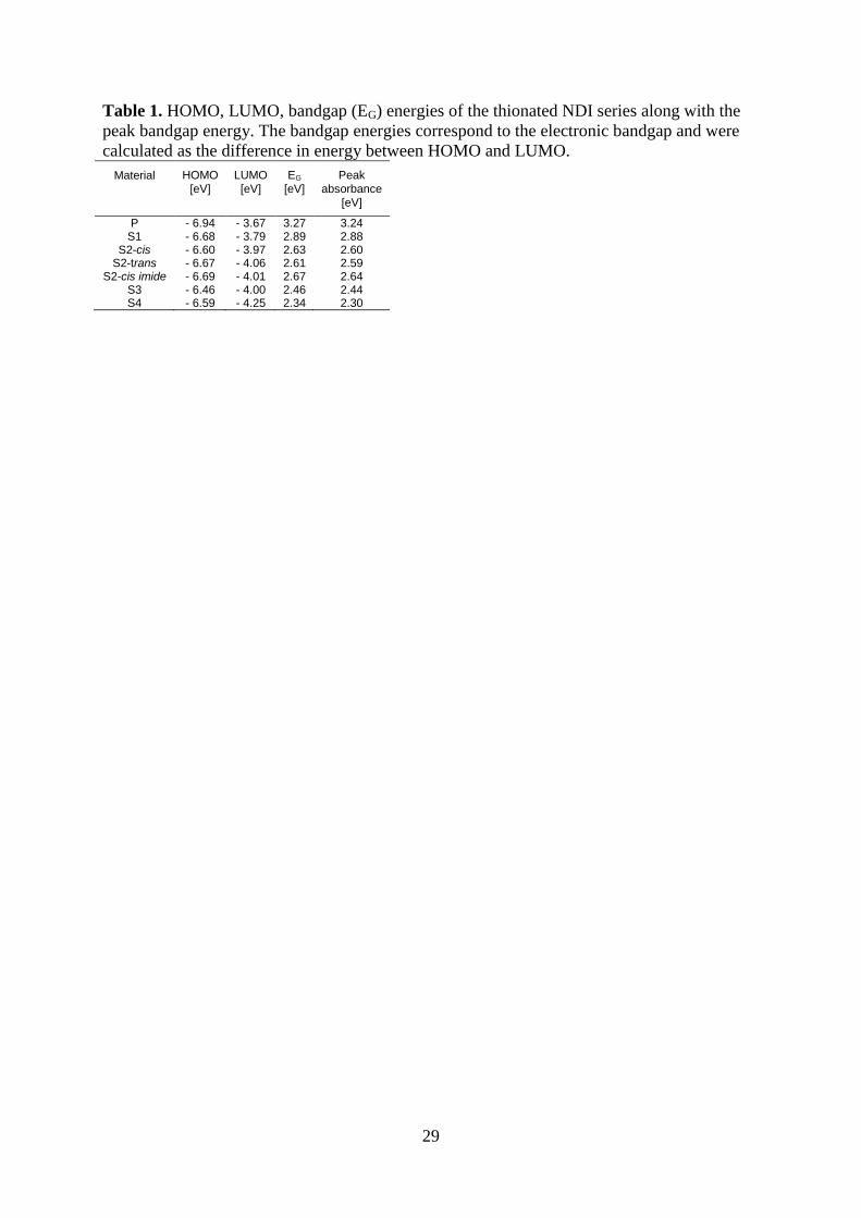
29
Table 1. HOMO, LUMO, bandgap (EG) energies of the thionated NDI series along with the
peak bandgap energy. The bandgap energies correspond to the electronic bandgap and were
calculated as the difference in energy between HOMO and LUMO.
Material HOMO
[eV]
LUMO
[eV]
EG
[eV]
Peak
absorbance
[eV]
P - 6.94 - 3.67 3.27 3.24 S1 - 6.68 - 3.79 2.89 2.88
S2-cis - 6.60 - 3.97 2.63 2.60 S2-trans - 6.67 - 4.06 2.61 2.59
S2-cis imide - 6.69 - 4.01 2.67 2.64 S3 - 6.46 - 4.00 2.46 2.44 S4 - 6.59 - 4.25 2.34 2.30
30
Table 2. Summary of the device parameters of spin-coated (SC) and blade-coated (BC)
TGBC OFETs based on the NDI6EH and thionated derivatives thereof.
Material Electron mobility
[cm2/Vs]
Threshold Voltage
[V] I on/off ratio
P SC 3.5 ± 0.4 10-2 7 2 5
BC 6.8 ± 0.6 10-2 12 ± 4 4
S1 SC 1.0 ± 0.1 10-3 15 ± 3 4
BC 1.1 ± 0.3 10-2 37 ± 3 5
S2-cis SC 1.66 ± 0.01 10-1 21.9 ± 0.3 6
BC 2.0 ± 0.2 10-1 20 ± 1 4
S2-trans SC 1.61 ± 0.09 10-1 5.8 ± 0.3 6
BC 1.8 ± 0.2 10-1 14 ± 3 5
S2-cis imide SC 2.8 ± 0.3 10-2 27.6 ± 0.5 5
BC 3.5 ± 0.9 10-2 35 ± 1 5
S3 SC 4.2 ± 0.9 10-2 23 ± 2 5
BC 1.2 ± 0.2 10-1 19 ± 2 6
S4 SC - - -
BC 2.5 ± 0.6 10-3 15.9 ± 0.2 4
31
Table 3. Summary of the unit cell parameters determined from spin-coated (SC) and blade-
coated (BC) films of NDI6EH and thionated derivatives thereof.
Material a
(Å)
b
(Å)
c
(Å)
()
()
()
P Primary SC 8.45 17.97 19.83 90.7 90.9 90.6
Secondary SC 11.19 17.23 16.89 92.0 95.1 88.5
Primary BC 8.49 18.03 20.09 90.4 91.0 89.6
Secondary BC 9.7 18.1 16.4 92 95 90
S1 SC 8.50 17.80 19.60 91.0 93.0 90.0
BC 8.6 18.0 19.60 90 92 90
S2-cis SC 8.75 18.04 19.56 91.0 93.9 89.1
BC 8.85 18.19 19.53 91 94.2 89.2
S2-trans Primary SC - - - - - -
Secondary SC - - - - - -
Primary BC 9.29 18.33 19.62 101.6 94.2 93.4
Secondary BC 10.93 18.09 18.67 95.4 93.8 90.2
S2-cis imide SC 8.85 18.03 19.41 90.6 92.9 89.5
BC 8.89 18.40 19.84 91 94.1 90.3
S3 SC 9.06 18.10 19.39 90.9 95.4 90.2
BC 9.15 18.27 19.31 90.5 95.4 90.2
S4 SC 9.0 18.0 20.0 95.0 95.0 90.0
BC - - - - - -
32
Supporting Information for
Thionation of naphthalene diimide molecules: Thin-film microstructure and transistor performance
Adam Welford,a Subashani Maniam,
b Eliot Gann,
a,c,+ Lars Thomsen,
c Steven J. Langford,
b
and Christopher R. McNeilla*
aDepartment of Materials Science and Engineering, Wellington Road, Clayton, Victoria, 3800, Australia
bSchool of Chemistry, Monash University, Wellington Road, Clayton, Victoria 3800, Australia
cAustralian Synchrotron, 800 Blackburn Road, Clayton, Victoria, 3168, Australia
*Corresponding author. E-mail: [email protected] +Present address: Materials Science and Engineering Division, National Institute of Standards and Technology,
Gaithersburg, MD 20899, USA
33
Figure S1. Output (a, c, e, g, i, k) and transfer (b, d, f, h, j, l) characteristics of spin-coated
TGBC transistors based on NDI6EH (a,b), S1 (c,d), S2-cis (e,f), S2-imide (g,h), S2-cis imide
(i,j), and S3 (k,l).
34
Figure S2. 20 m 20 m AFM images of spin-coated and blade coated films.
35
Figure S3. AFM height analysis of a blade-coated S2 film showing terracing with a step
height of ~ 1.7 nm derived from peak spearation in the height histogram.
36
Figure S4. Angle-resolved NEXAFS spectra of spin-coated films of (a) the parent molecule,
(b) S1, (c), S2-cis, (d) S2-trans, (e) S2-cis imide, (f) S3, (g) S4.
37
Figure S5. Angle-resolved NEXAFS spectra of blade-coated films of (a) the parent molecule,
(b) S1, (c), S2-cis, (d) S2-trans, (e) S2-cis imide, (f) S3, (g) S4.
38
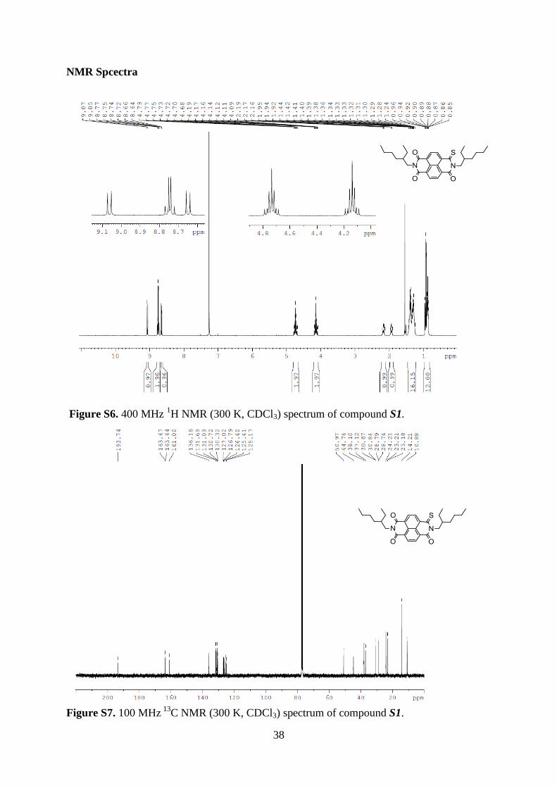
NMR Spcectra
Figure S6. 400 MHz
1H NMR (300 K, CDCl3) spectrum of compound S1.
Figure S7. 100 MHz
13C NMR (300 K, CDCl3) spectrum of compound S1.
39
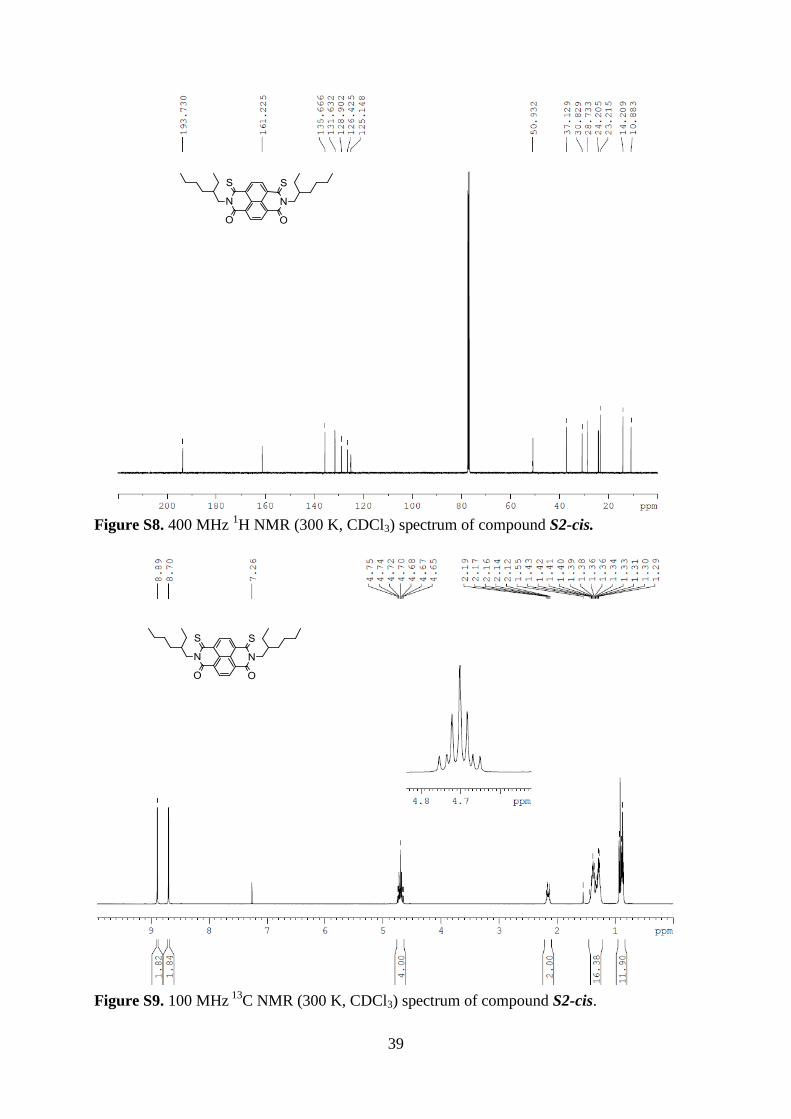
Figure S8. 400 MHz
1H NMR (300 K, CDCl3) spectrum of compound S2-cis.
Figure S9. 100 MHz
13C NMR (300 K, CDCl3) spectrum of compound S2-cis.
40
Figure S10. 400 MHz
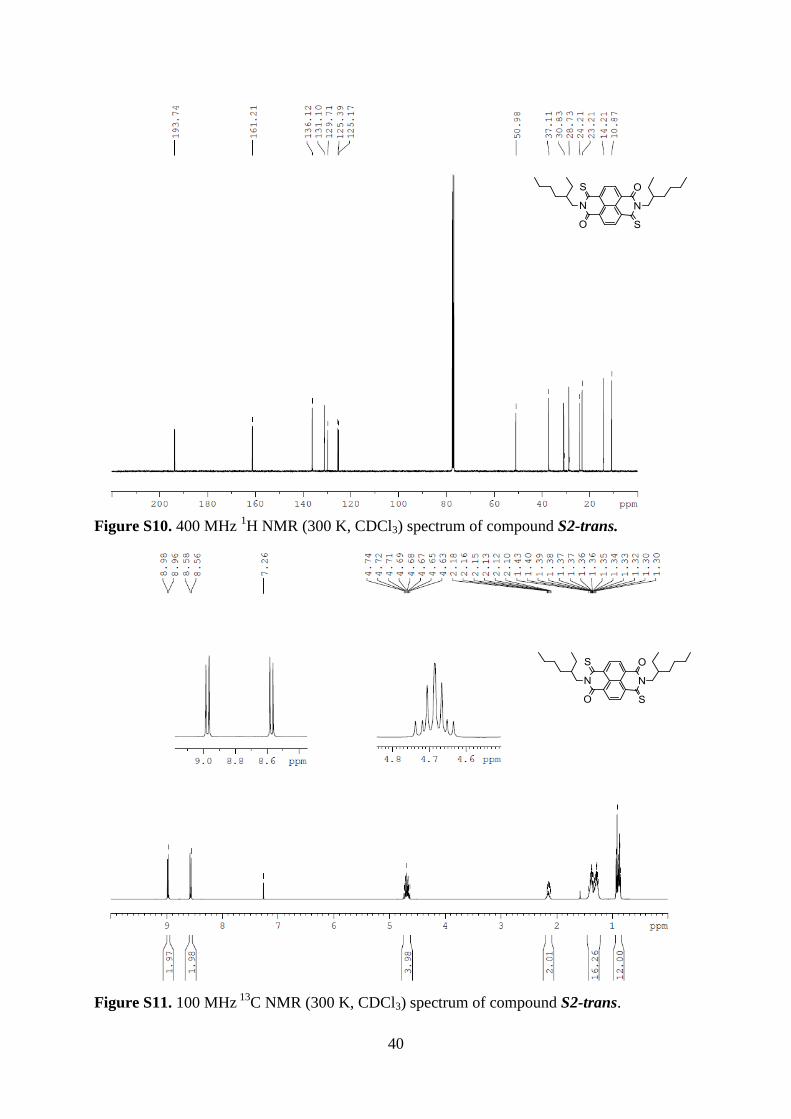
1H NMR (300 K, CDCl3) spectrum of compound S2-trans.
Figure S11. 100 MHz
13C NMR (300 K, CDCl3) spectrum of compound S2-trans.
41
Figure S12. 400 MHz
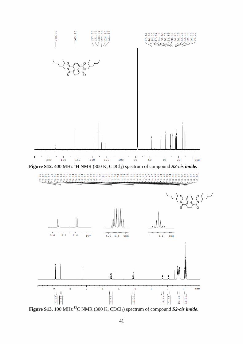
1H NMR (300 K, CDCl3) spectrum of compound S2-cis imide.
Figure S13. 100 MHz
13C NMR (300 K, CDCl3) spectrum of compound S2-cis imide.
42
Figure S14. 400 MHz
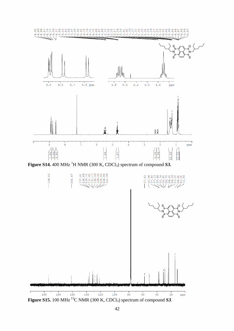
1H NMR (300 K, CDCl3) spectrum of compound S3.
Figure S15. 100 MHz
13C NMR (300 K, CDCl3) spectrum of compound S3.
43
Figure S16. 400 MHz
1H NMR (300 K, CDCl3) spectrum of compound S4.
Figure S17. 100 MHz
13C NMR (300 K, CDCl3) spectrum of compound S4.

44


![Supporting Information Pyrrole[3,2-d:4,5-d′]bisthiazole-Bridged- … · 2013-11-07 · 1 Supporting Information for Pyrrole[3,2-d:4,5-d′]bisthiazole-Bridged-Bis(naphthalene diimide)s](https://img.dokumen.tips/doc/110x75/5edca713ad6a402d666768ee/supporting-information-pyrrole32-d45-dabisthiazole-bridged-2013-11-07.jpg)