Embed Size (px)
Citation preview
Thin Film Quantitationof Chemistry and Thickness Using EPMA
John Donovan Micro Analytical Facility
CAMCOR (Characterization of Advanced Materials in Oregon)
University of OregonEugene, OR
(541)[email protected]
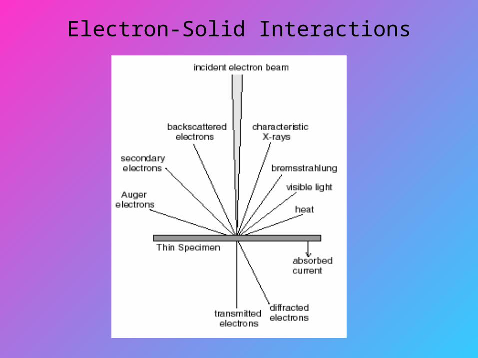
Electron-Solid Interactions
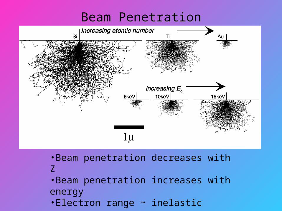
Beam Penetration
•Beam penetration decreases with Z •Beam penetration increases with energy•Electron range ~ inelastic processes•Electron scattering (aspect) ~ elastic processes

X-ray Generation
From Wittke, 1997-2003
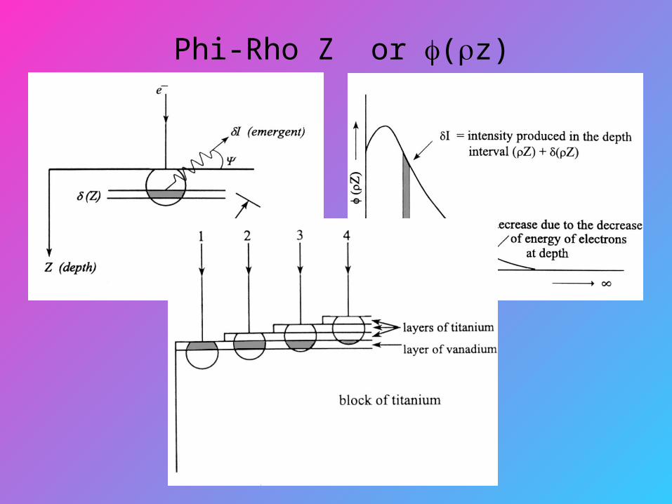
Phi-Rho Z or (z)
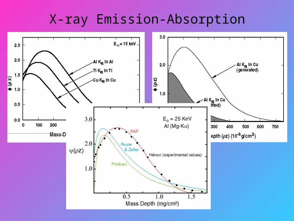
X-ray Emission-Absorption
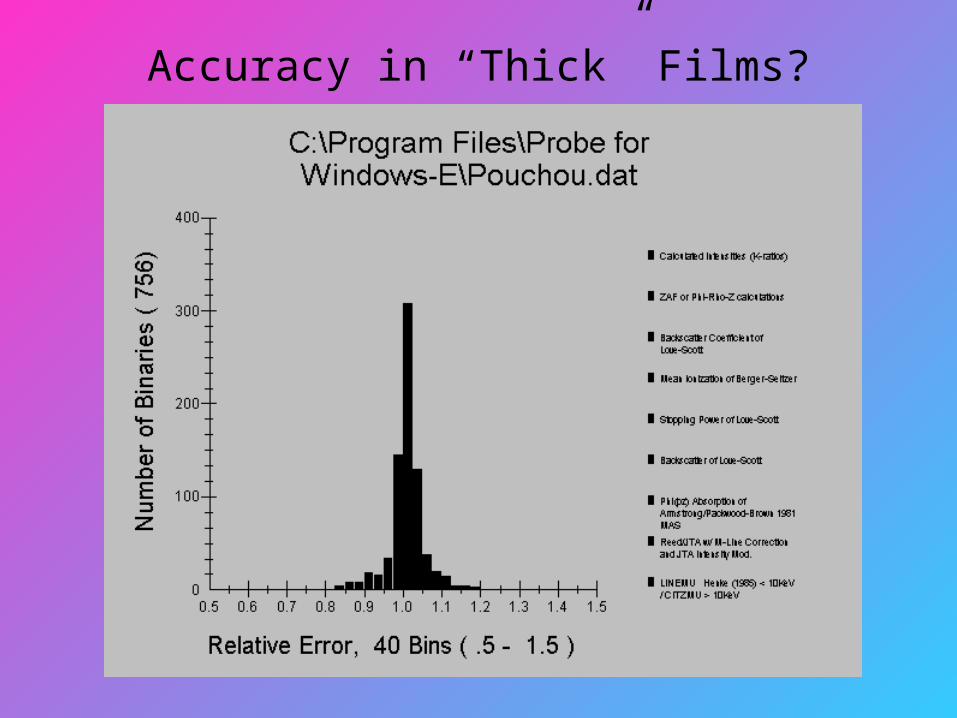
Accuracy in “Thick” Films?

The Future?
Monte-Carlo calculations (using an iterative geometric
model)
Will require computations roughly 106 faster than current
processors

What is a Thin Film (for EPMA)?
•Films greater than 5-10 um can be considered “infinitely thick”•Treat it like a “rock” (just kidding)
•Films less than 500 angstroms are “ultra-thin”•Use MVA (and take special precautions: surface contamination, plasma cleaning prior to analysis)
•Films between 5000-500 angstroms are “normal”•Use MVA (multi-voltage analysis) and model geometry
John Donovan:
always measure oxygen
hydrocarbon contamination
plasma cleaning prior to analysis
John Donovan:
always measure oxygen
hydrocarbon contamination
plasma cleaning prior to analysis
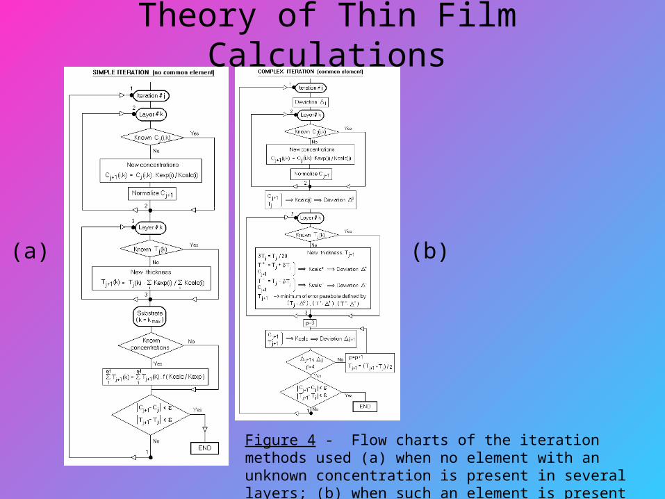
Theory of Thin Film Calculations
Figure 4 - Flow charts of the iteration methods used (a) when no element with an unknown concentration is present in several layers; (b) when such an element is present in several layers. From Thiot
(a) (b)
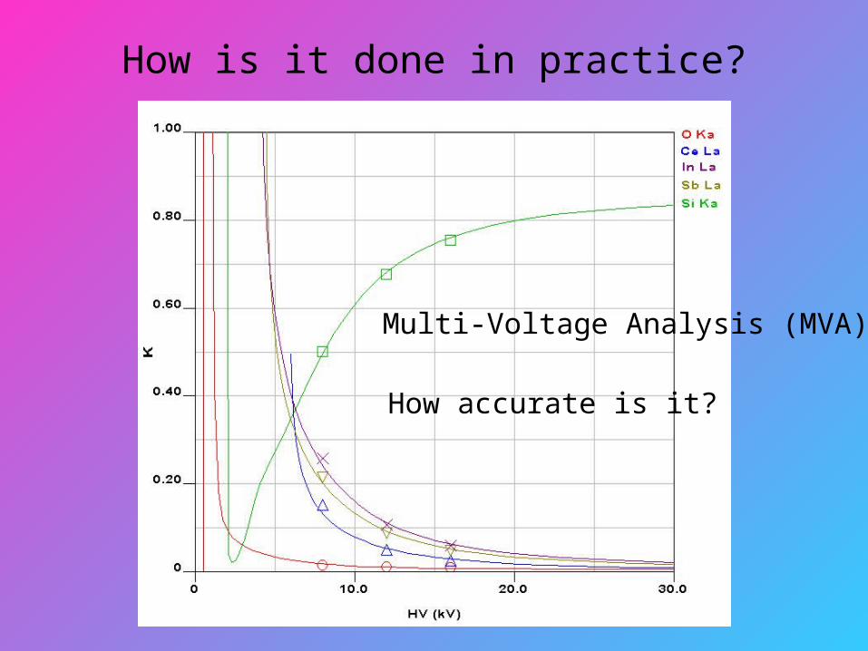
How is it done in practice?
Multi-Voltage Analysis (MVA)
How accurate is it?
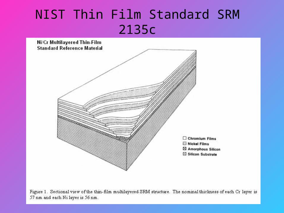
NIST Thin Film Standard SRM 2135c
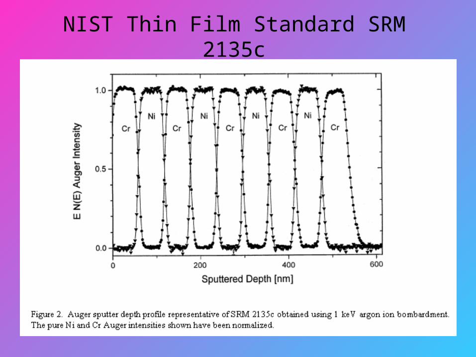
NIST Thin Film Standard SRM 2135c
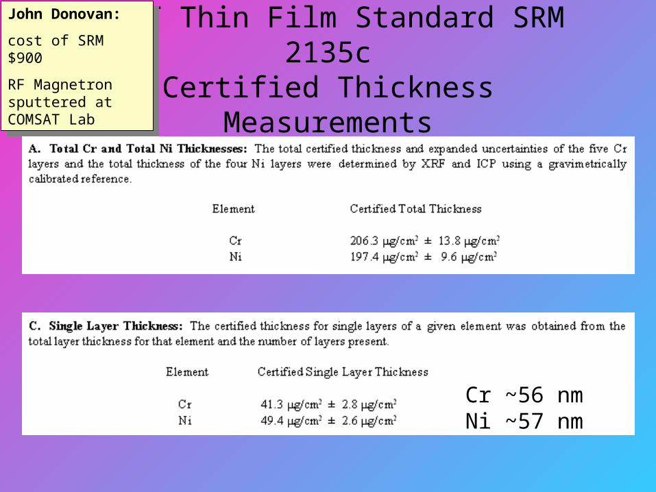
NIST Thin Film Standard SRM 2135cCertified Thickness Measurements
Cr ~56 nmNi ~57 nm
John Donovan:
cost of SRM $900
RF Magnetron sputtered at COMSAT Lab
John Donovan:
cost of SRM $900
RF Magnetron sputtered at COMSAT Lab
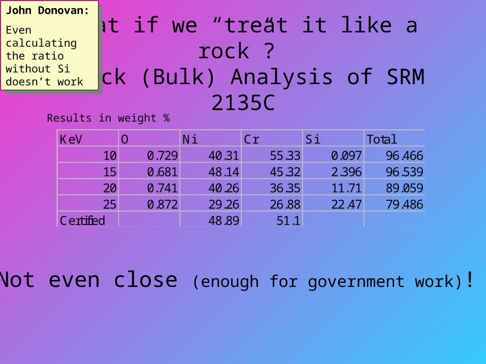
What if we “treat it like a rock”? Thick (Bulk) Analysis of SRM 2135C
KeV O Ni Cr Si Total10 0.729 40.31 55.33 0.097 96.46615 0.681 48.14 45.32 2.396 96.53920 0.741 40.26 36.35 11.71 89.05925 0.872 29.26 26.88 22.47 79.486
Certified 48.89 51.1
Results in weight %
Not even close (enough for government work)!
John Donovan:
Even calculating the ratio without Si doesn’t work
John Donovan:
Even calculating the ratio without Si doesn’t work
NIST Thin Film Standard SRM 2135c
0 10.0 20.0 30.0
HV (kV)
0
0.20
0.40
0.60
0.80
1.00K
O KaNi KaCr KaSi Ka
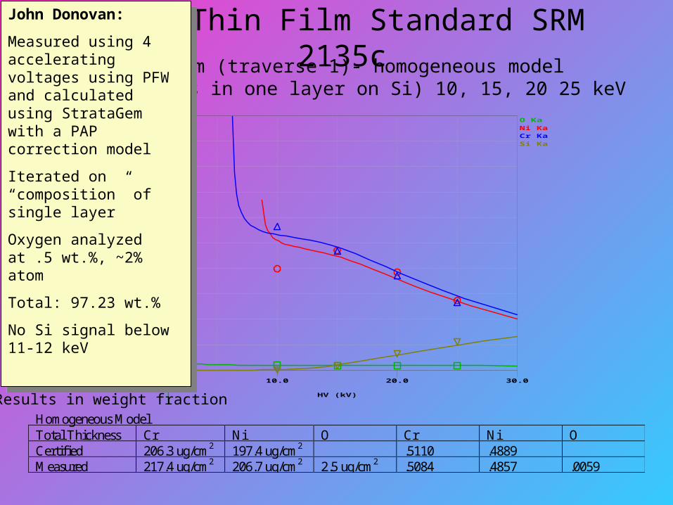
Thin Film (traverse 1)- homogeneous model (all elements in one layer on Si) 10, 15, 20 25 keV
Homogeneous ModelTotal Thickness Cr Ni O Cr Ni OCertified 206.3 ug/cm2 197.4 ug/cm2 .5110 .4889Measured 217.4 ug/cm2 206.7 ug/cm2 2.5 ug/cm2 .5084 .4857 .0059
Results in weight fraction
John Donovan:
Measured using 4 accelerating voltages using PFW and calculated using StrataGem with a PAP correction model
Iterated on “composition” of single layer
Oxygen analyzed at .5 wt.%, ~2% atom
Total: 97.23 wt.%
No Si signal below 11-12 keV
John Donovan:
Measured using 4 accelerating voltages using PFW and calculated using StrataGem with a PAP correction model
Iterated on “composition” of single layer
Oxygen analyzed at .5 wt.%, ~2% atom
Total: 97.23 wt.%
No Si signal below 11-12 keV

NIST Thin Film Standard SRM 2135cThin Film (traverse 1)- homogeneous model
(all elements in one layer on Si) 15, 20 25 keV(same as above but without 10 keV data)
0 10.0 20.0 30.0
HV (kV)
0
0.20
0.40
0.60
0.80
1.00K
O KaNi KaCr KaSi Ka
Homogeneous Model (without 10 keV data)Total Thickness Cr Ni O Cr Ni OCertified 206.3 ug/cm2 197.4 ug/cm2 .5110 .4889Measured 216.4 ug/cm2 205.0 ug/cm2 2.37 ug/cm2 .5106 .4838 .0056
John Donovan:
Total 99.73 wt.%
John Donovan:
Total 99.73 wt.%
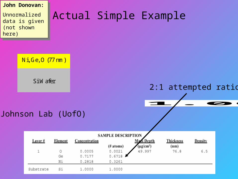
Actual Simple Example
0 10.0 20.0 30.0
HV (kV)
0
0.20
0.40
0.60
0.80
1.00
K
O Ka
Si Ka
Ni KaGe La
Ni, Ge, O (77 nm)
Si Wafer
Johnson Lab (UofO)
John Donovan:
Unnormalized data is given (not shown here)
John Donovan:
Unnormalized data is given (not shown here)
2:1 attempted ratio
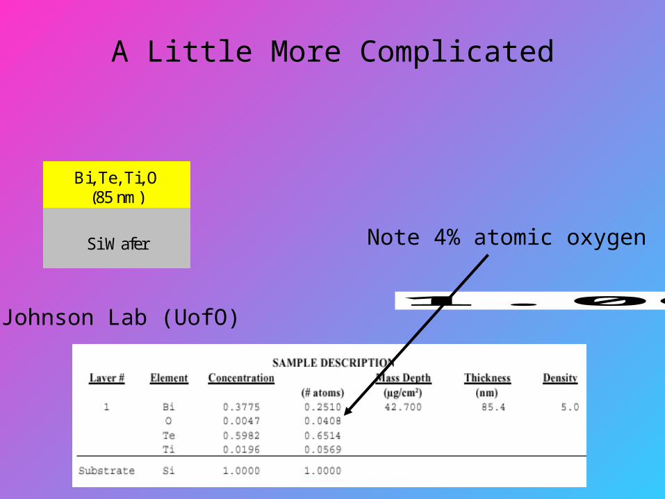
A Little More Complicated
0 10.0 20.0 30.0
HV (kV)
0
0.20
0.40
0.60
0.80
1.00
K
O Ka
Si Ka
Bi Ma
Te La
Ti Ka
Bi, Te, Ti, O(85 nm)
Si Wafer
Johnson Lab (UofO)
Note 4% atomic oxygen
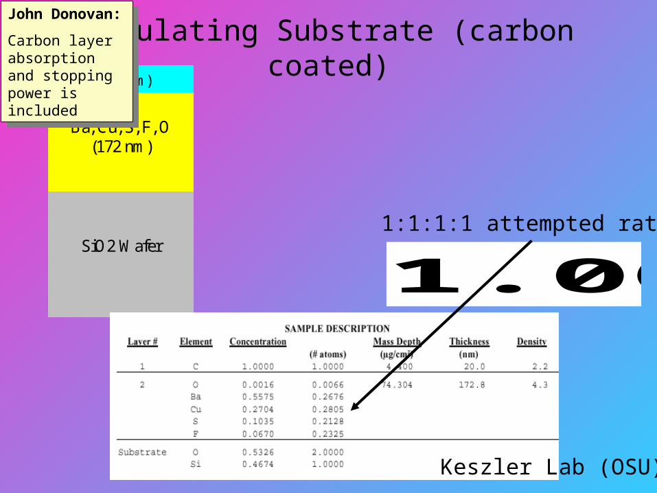
Insulating Substrate (carbon coated)
0 10.0 20.0 30.0
HV (kV)
0
0.20
0.40
0.60
0.80
1.00
K
O KaBa LaCu Ka
Si Ka
F Ka
C Ka
S Ka
Ba, Cu, S, F, O(172 nm)
SiO2 Wafer
C (20 nm)
Keszler Lab (OSU)
John Donovan:
Carbon layer absorption and stopping power is included
John Donovan:
Carbon layer absorption and stopping power is included
1:1:1:1 attempted ratio
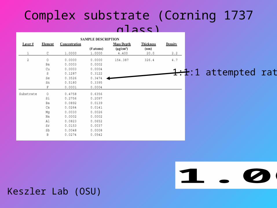
Complex substrate (Corning 1737 glass)
0 10.0 20.0 30.0
HV (kV)
0
0.20
0.40
0.60
0.80
1.00
K
O KaBa LaCu KaS KaSe LaSi KaSn LaF KaCa KaMg KaAl KaSr KaSb KaB KaC Ka
Na Ka
Keszler Lab (OSU)
1:1:1 attempted ratio
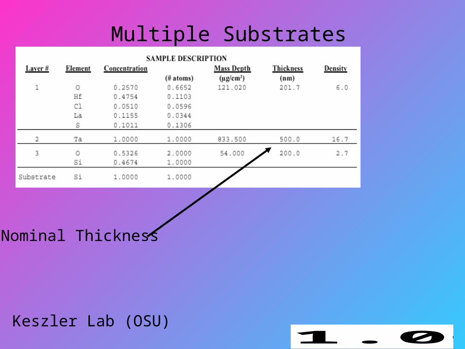
Multiple Substrates
0 10.0 20.0 30.0
HV (kV)
0
0.20
0.40
0.60
0.80
1.00
K
O Ka
Si Ka
Hf MaCl Ka
La LaS Ka
Ta Ka
Keszler Lab (OSU)
Nominal Thickness
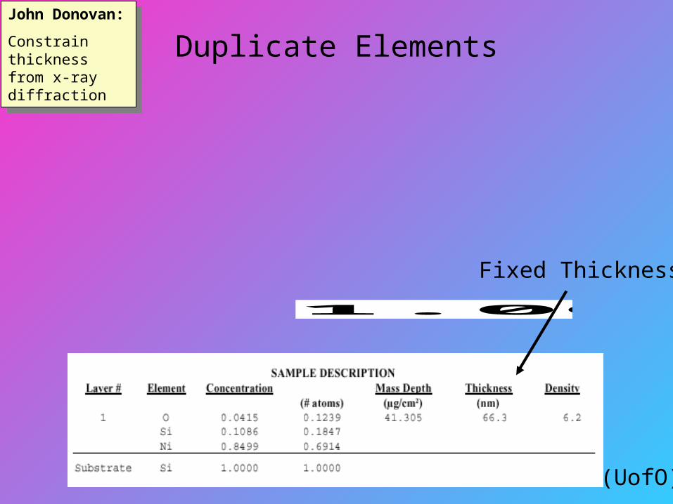
Duplicate Elements
0 10.0 20.0 30.0
HV (kV)
0
0.20
0.40
0.60
0.80
1.00
K
O Ka
Si Ka
Ni Ka
Johnson Lab (UofO)
John Donovan:
Constrain thickness from x-ray diffraction
John Donovan:
Constrain thickness from x-ray diffraction
Fixed Thickness

Duplicate Elements By Stoichiometry to Obtain Mass Thickness
Johnson Lab (UofO)
0 10.0 20.0 30.0
HV (kV)
0
0.20
0.40
0.60
0.80
1.00
K
Si Ka
O Ka
Al KaZn Ka
Conclusions
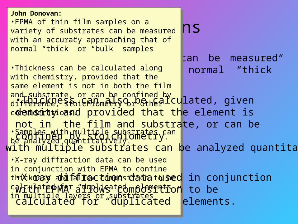
•A variety of substrates can be measured with accuracy approaching normal “thick” samples
John Donovan:•EPMA of thin film samples on a variety of substrates can be measured with an accuracy approaching that of normal “thick” or “bulk” samples
•Thickness can be calculated along with chemistry, provided that the same element is not in both the film and substrate, or can be confined by difference, stoichiometry or other considerations.
•Samples with multiple substrates can be analyzed quantitatively.
•X-ray diffraction data can be used in conjunction with EPMA to confine thickness and allow composition to be calculated for “duplicated” elements in multiple layers or substrates
•X-ray diffraction data used in conjunction with EPMA allows composition to be calculated for “duplicated” elements.
•Samples with multiple substrates can be analyzed quantitatively.
•Thickness can also be calculated, given density and provided that the element is not in the film and substrate, or can be confined by stoichiometry.