Embed Size (px)
Citation preview

Thin Film Formation of a Solution ProcessedPentacene
Daniel C Huang
Electrical Engineering and Computer SciencesUniversity of California at Berkeley
Technical Report No. UCB/EECS-2009-74
http://www.eecs.berkeley.edu/Pubs/TechRpts/2009/EECS-2009-74.html
May 20, 2009

Copyright 2009, by the author(s).All rights reserved.
Permission to make digital or hard copies of all or part of this work forpersonal or classroom use is granted without fee provided that copies arenot made or distributed for profit or commercial advantage and that copiesbear this notice and the full citation on the first page. To copy otherwise, torepublish, to post on servers or to redistribute to lists, requires prior specificpermission.

Thin Film Formation of a Solution Processed Pentacene
by
Daniel Huang
B.S. (University of California, Berkeley) 2002
M.S. (University of California, Berkeley) 2006
A dissertation submitted in partial satisfaction of the
Requirements for the degree of
Doctor of Philosophy
in
Electrical Engineering and Computer Sciences
in the
Graduate Division
of the
University of California, Berkeley
Committee in charge:
Professor Vivek Subramanian, Chair
Professor Tsu-Jae King Liu
Professor Oscar Dubon
Spring 2009

The dissertation of Daniel Chien-Hau Huang is approved:
Chair Date
Date
Date
University of California, Berkeley

1
Abstract
Thin Film Formation of a Solution Processed Pentacene
by
Daniel Huang
Doctor of Philosophy in Electrical Engineering and Computer Sciences
University of California, Berkeley
Professor Vivek Subramanian, Chair
Pentacene has one of the highest carrier mobility among organic semiconductors.
Unfortunately, due to its tight packing density, giving it its high mobility, pentacene does
not readily dissolve in common solvents, making it difficult to incorporate into printed
electronics. Solution processable pentacene through a precursor route is a promising
method of incorporating pentacene into printed electronics. Here, the thin film formation
of pentacene through a precursor route is detailed. Specifically, the thin film formation
of pentacene on oxide is compared with thin film formation of pentacene on oxide
through evaporation methods. Then thin film formation of pentacene through the
precursor is detailed and compared on different substrates important to printed
electronics. Finally, the performance of pentacene thin film transistors is tested by using
different heat treatments for processing the pentacene precursor. The heat treatments
were based on the thin film studies of pentacene thin film formation and seek to optimize
pentacene TFT performance.

i
Acknowledgements
Funding for this work was from SRC. This dissertation was made possible
through the talents and generous contribution of many extraordinary people at UC
Berkeley. Jean Frechet’s group in the department of Chemistry has been a great for
support in organic chemistry. In particular Clayton Mauldin has always been available
for discussions and equipment training. In the Organic Electronics Lab, special thanks to
Shong Yin and Kanan Puntambekar for trememdous help in X-ray analysis. Thanks also
to Steven Volkman and Kinyip Phoa for help with materials characterization. AFM work
would not have be possible without the aid of Alejandro de la Fuente Vornbrock. Thanks
to Frank Liao who helped me in whatever way was humanly possible for him. In
addition, thanks to Paul Chang and Tuyen Le who taught me the ins and outs of research
as I was getting started. Of course, many thanks to my advisor Vivek Subramanian who
has been mentor these past years and taught me not only research but also football.

ii
Dedicated to my cousin Titus Jahng
Somehow he also decided to study engineering

iii
Table of Contents
1 Introduction ................................................................................................................. 1
1.1 Printed Electronics ............................................................................................... 2
1.2 Organic Semiconductors for Printed Electronics ................................................ 5
1.2.1 Conferring Solubility to Organic Semiconductors ....................................... 7
1.3 Inorganic Nanoparticles ..................................................................................... 13
1.4 Organic Thin film Transistors ............................................................................ 14
1.4.1 Operation of OTFTs .................................................................................... 16
1.4.2 Transport in OTFTs .................................................................................... 19
1.5 Organization ....................................................................................................... 24
1.6 References .......................................................................................................... 27
2 Experimental Methods and Characterization Techniques ......................................... 32
2.1 OTFT Fabrication and Testing ........................................................................... 32
2.1.1 OTFT Fabrication ....................................................................................... 32
2.1.2 Electrical testing of OTFT .......................................................................... 35
2.1.3 Mobility extraction...................................................................................... 36
2.2 Scanning Electron Microscopy (SEM) .............................................................. 38
2.3 Atomic Force Microscopy (AFM) ..................................................................... 41
2.4 Glancing Angle X-ray Diffraction (GIXD) ........................................................ 44
2.5 UV-vis Spectroscopy.......................................................................................... 50
2.6 References .......................................................................................................... 54
3 The Pentacene Precursor Reaction ............................................................................ 56
3.1 Background ........................................................................................................ 56

iv
3.2 Experimental Procedures.................................................................................... 58
3.3 Experimental Results.......................................................................................... 59
3.4 Discussion .......................................................................................................... 67
3.5 Conclusion .......................................................................................................... 69
3.6 References .......................................................................................................... 70
4 The Pentacene Thin-film growth on SiO2 from Pentacene precursor ....................... 71
4.1 Background ........................................................................................................ 71
4.2 Growth of Pentacene on SiO2 through Evaporation........................................... 71
4.3 Experimental Procedures.................................................................................... 75
4.3.1 Preparing Pentacene precursor on Oxide .................................................... 75
4.3.2 Heating of conditions of samples to trace pentacene growth ..................... 75
4.3.3 SEM imaging .............................................................................................. 76
4.3.4 AFM imaging .............................................................................................. 77
4.3.5 GIXD........................................................................................................... 77
4.4 Results ................................................................................................................ 78
4.4.1 Qualitative SEM results .............................................................................. 78
4.4.2 Quantitative SEM results ............................................................................ 86
4.4.3 AFM results ................................................................................................ 91
4.4.4 GIXD Results .............................................................................................. 95
4.5 Discussion .......................................................................................................... 99
4.6 Conclusion ........................................................................................................ 104
4.7 References ........................................................................................................ 106
5 Pentacene Precursor Growth on other Substrates .................................................... 108

v
5.1 Background ...................................................................................................... 108
5.2 Theory (Comparison of Substrates) ................................................................. 110
5.3 Experimental .................................................................................................... 113
5.3.1 Preparation of substrates ........................................................................... 113
5.4 Results and Discussion ..................................................................................... 115
5.4.1 Qualitative SEM results ............................................................................ 115
5.4.2 Pentacene Stability Calculation ................................................................ 118
5.4.3 Quantitative Results and Discussion ......................................................... 120
5.5 Conclusions ...................................................................................................... 125
5.6 References ........................................................................................................ 126
6 Heat Treatments of Pentacene Precursor ................................................................. 128
6.1 Background ...................................................................................................... 128
6.2 Experimental .................................................................................................... 130
6.2.1 SEM sample preparation ........................................................................... 130
6.2.2 Pentacene TFT preparation ....................................................................... 131
6.2.3 Heat treatment of TFT and SEM samples................................................. 131
6.2.4 Sample Analysis........................................................................................ 136
6.3 Results and Discussion ..................................................................................... 136
6.3.1 One-step Heating (C1 and C2.1) ............................................................... 136
6.3.2 Post-processing anneal .............................................................................. 142
6.3.3 Step-down Heating.................................................................................... 145
6.3.4 Step-up results ........................................................................................... 151
6.3.5 Quenching Control (C2.2) ........................................................................ 154

vi
6.4 Conclusions ...................................................................................................... 157
6.5 References ........................................................................................................ 159
7 Conclusions and Suggestions for Future Work ....................................................... 162
7.1 References ........................................................................................................ 167
9 Appendix (SAP synthesis) ....................................................................................... 168
9.1 Introduction ...................................................................................................... 168
9.2 Chemicals Required ......................................................................................... 168
9.3 Laboratory Equipment...................................................................................... 168
9.4 Overview .......................................................................................................... 169
9.5 Pentacene Sublimation Purification ................................................................. 170
9.5.1 Preparation ................................................................................................ 170
9.5.2 Sublimation ............................................................................................... 170
9.6 Diels-Alder Adduct synthesis (NSO) ............................................................... 171
9.6.1 Preparation ................................................................................................ 171
9.6.2 Synthesis ................................................................................................... 171
9.7 Diels-Alder Reaction (SAP synthesis) ............................................................. 173
9.7.1 Preparation ................................................................................................ 173
9.7.2 Synthesis ................................................................................................... 173
9.8 SAP purification ............................................................................................... 174
9.8.1 Preparation ................................................................................................ 174
9.8.2 Flash Column Purification ........................................................................ 174
9.9 References ........................................................................................................ 177

vii
List of Figures
Figure 1-1: An all additive printing process. ..................................................................... 4
Figure 1-2: Printed electronics paradigm ........................................................................... 5
Figure 1-3: Different yypes of organic semiconductors .................................................... 7
Figure 1-4: The tradition herring-bone structure of pentacene .......................................... 9
Figure 1-5: Modified oligothiophenes ............................................................................. 10
Figure 1-6: Pentacene with TIPS side groups .................................................................. 11
Figure 1-7: Packing of TIPS pentacene ........................................................................... 11
Figure 1-8: The first soluble pentacene precursors .......................................................... 12
Figure 1-9: The concerted Diels-Alder reaction .............................................................. 12
Figure 1-10: The Diels-Alder reaction for pentacene ...................................................... 13
Figure 1-11: Different OTFT configurations ................................................................... 16
Figure 1-12: Operation of a p-OTFT ............................................................................... 17
Figure 1-13: IV Characteristics of a typical OTFT. ......................................................... 18
Figure 1-14: Alkadiene .................................................................................................... 20
Figure 2-1: Substrate-gated TFT process ......................................................................... 34
Figure 2-2: Cross-section view of the substrate-gated OTFT process ............................. 34
Figure 2-3: Contacting source/drain pads on TFTs ......................................................... 35
Figure 2-4: Example of SEM images............................................................................... 39
Figure 2-5: Thresholding in SEM images. ....................................................................... 40
Figure 2-6: A typical AFM tip setup................................................................................ 42
Figure 2-7: AFM image analyzing the profile of a cross-section .................................... 44
Figure 2-8: Schematic of GIXD setup ............................................................................. 45

viii
Figure 2-9: GIXD of pentacene films .............................................................................. 46
Figure 2-10: 100 plane seen in GIXD. ............................................................................. 48
Figure 2-11: Peak doubling .............................................................................................. 49
Figure 2-12: Diagram of Beer-Lambert absorption of an incident beam. ....................... 50
Figure 2-13: UV-vis absorption spectrum of chemical A and B ..................................... 52
Figure 2-14: UV-vis absorption spectrum of with both A and B present. ....................... 53
Figure 3-1: UV-vis absorption spectrum of pentacene precursor and pentacene ............ 60
Figure 3-2: The change of absorbance as the SAP reaction proceeds. ............................ 61
Figure 3-3: Disappearance of SAP at 1300C traced by UV-vis. ...................................... 62
Figure 3-4: log-linear plot of SAP disappearance at 1300C ............................................. 63
Figure 3-5: SAP disappearance at 1600C ......................................................................... 64
Figure 3-6: linear-linear plot of SAP disappearance at 1900C ......................................... 65
Figure 3-7: Arrhenius relationship in order to estimate activation energy. ..................... 66
Figure 4-1: Summary of thickness dependent thin film growth of pentacene on oxide .. 73
Figure 4-2: Calculation of characteristic length ............................................................... 77
Figure 4-3: Nucleation of pentacene (1250C, 30s)........................................................... 79
Figure 4-4: Development of pentacene processed at 1250C ............................................ 79
Figure 4-6: High temperature nucleation. (1500C, 15s) ................................................... 81
Figure 4-7: Crystal grown on the high temperature nucleation. (1500C, 45s) ................. 82
Figure 4-8: Dewetting on fully develop films. (1800C,1min) .......................................... 83
Figure 4-9: Mixed nuclation (1400C, 1min) .................................................................... 84
Figure 4-10: Crystal grown on mixed nucleation (1400C, 4min). ................................... 85
Figure 4-11: Fully reacted pentacene film (1400C, 32min). ............................................ 85

ix
Figure 4-12 Fully reacted pentacene film (1500C, 16 min) ............................................. 86
Figure 4-13: Density of nucleation sites at 1250C ........................................................... 87
Figure 4-14: Density of nucleation sites at 1600C ........................................................... 88
Figure 4-15: High and low temperature nucleation sites. ................................................ 88
Figure 4-16: The effect of temperature on the island sizes .............................................. 89
Figure 4-17: The effect of temperature on the time of lateral island growth stops. ........ 91
Figure 4-18: AFM of low temperature islands ................................................................ 92
Figure 4-19: AFM of a high temperature nucleus. (1600C, 4s) ....................................... 93
Figure 4-20: AFM a fully reacted film showing dewetting. (1800C, 1min) .................... 95
Figure 4-21: 2D GIXD plot for a film processed at 1250C .............................................. 96
Figure 4-22: 2D GIXD plot for a film processed at 1400C .............................................. 97
Figure 4-23: 2D GIXD plot for a film processed at 1600C .............................................. 97
Figure 4-24: 2D GIXD plot for a film processed at 1800C .............................................. 98
Figure 4-25: Crystallize size due to processing temperature ........................................... 99
Figure 4-26: Time-temperature dependency on pentacene film growth from SAP. ...... 103
Figure 5-1: Nucleaction on HMDS substrates ............................................................... 116
Figure 5-2: Pentacene processed on PVP and silver at 1250C ....................................... 117
Figure 5-3: Dewetting of pentacene. .............................................................................. 117
Figure 5-4: Film coverage by substrate at 1800C........................................................... 119
Figure 5-5: Calculation of relative free-energy based on dewetting .............................. 119
Figure 5-6: Nucleation density for films processed at 1250C. ....................................... 121
Figure 5-7: Nucleation density for films processed at 1400C. ....................................... 121
Figure 5-8: Characteristic length of islands on films processed at 1250C. .................... 122

x
Figure 5-9: Characteristic length of islands on films processed at 1400C. .................... 122
Figure 5-10: RMS roughness of films processed at 1250C. ........................................... 123
Figure 5-11: RMS roughness of films processed at 1800C. ........................................... 123
Figure 6-1: One-step 1250C from experiment 1 and 2. .................................................. 137
Figure 6-2: One-step 1400C from experiment 1 and 2. .................................................. 137
Figure 6-3: C1 TFT results ............................................................................................ 139
Figure 6-4: C.2 TFT results ........................................................................................... 140
Figure 6-5: SEM forPost-processing anneal. ................................................................. 143
Figure 6-6: I-V for Post-processing anneal .................................................................... 145
Figure 6-7: SEM for Step-down heating ........................................................................ 147
Figure 6-8: I-V for Step-down heating. ......................................................................... 148
Figure 6-10: SEM for ste-up heating. ............................................................................ 152
Figure 6-11: I-V for Step-up heating ............................................................................. 153
Figure 6-12: 160 heating series ...................................................................................... 154
Figure 6-13: Quench control .......................................................................................... 156

xi
List of Tables
Table 3-1: List of all the temperature time conditions used for UV-vis anaylsis ............ 59
Table 3-2: Reaction rates for different temperatures ....................................................... 66
Table 4-1: Sample conditions for SEM ........................................................................... 76
Table 4-2: Sample conditions for GIXD .......................................................................... 77
Table 4-3: Roughness of films ......................................................................................... 95
Table 5-1: Heating conditions for all samples ............................................................... 114
Table 5-2: Ranking of substrate relative free-energy compared to SiO2. ...................... 119
Table 6-1: Experiment 1. ............................................................................................... 134
Table 6-2: Experiment 2.. .............................................................................................. 136
Table 9-1 Chemicals Properties of Chemicals ............................................................... 176
Table 9-3: Mole ratios for Diel-Alder reaction .............................................................. 176

xii
List of Equations
Equation 1-1: Square-law equations. ............................................................................... 18
Equation 1-2: MTR equations .......................................................................................... 23
Equation 2-1: Square-law equations ................................................................................ 36
Equation 2-2: Mobility in saturation ............................................................................... 37
Equation 2-3: Mobility in triode ...................................................................................... 37
Equation 2-4: Bragg’s Law .............................................................................................. 44
Equation 2-5: Beer-Lambert equation ............................................................................. 51
Equation 2-6: Absorbance for two chemicals .................................................................. 51
Equation 3-1 ...................................................................................................................... 62
Equation 3-3 ...................................................................................................................... 63
Equation 3-4 ...................................................................................................................... 65
Equation 3-5: Avrami equation ........................................................................................ 68
Equation 5-1: Definition of the equilibrium constant .................................................... 112
Equation 5-2: Equation for Gibb’s free energy.............................................................. 112

1
1 Introduction
Printed electronics has been an area of increased research in these past years. It
promises to reduce the cost of manufacturing electronics, which would allow for low-cost
electronics in an application space which currently does not exist. Applications can
include flexible displays,1 electronic noses,2 RFID tags3 and e-textiles.4 All these
applications do not necessarily require high switching speeds; instead they require
flexible substrates and low cost manufacturing.
Printed electronics is a technology which uses a different paradigm than
traditional semiconductors. While silicon technology strives for electronics with high
switching speeds and high integration density to fit in a small area, printed electronics is
useful for applications where small areas, high speed and high integration are not
necessary. The purpose of printed electronics is not to compete with current silicon
based semiconductors, instead it fills a different application space which current silicon
based semiconductors does not address. Specifically, the promise of printed electronics
is to create low-cost electronics.
Many people equate printed electronics with organic electronics. Strictly
speaking organic electronics does not have to be printed, however a great driver in
organic electronics is use printing technology. Even though printed electronics does not
have to use organic materials, however a great portion of materials used for printed

2
electronics is organic. It can be said that it was the discovery of organic semiconductors
that allowed for printed electronics to be possible.
This thesis deals with a pentacene precursor for use as a semiconducting material
in printed electronics, specifically for a TFT. This chapter will first talk about printed
electronics and the place where printed electronics falls in the world of electronics. Next,
the materials used for printed electronics is covered. Specifically, the organic
semiconductor pentacene and the pentacene precursor will be introduced. Finally, the
general organization of this thesis is outlined.
1.1 Printed Electronics
As stated before, printed electronics fills the application space which tradition
silicon-based technology does not fill and even spaces which have not yet been thought
of because the technology was not present. Specifically it fills the space of low-cost and
disposable electronics. Disposable electronics allows for the thought of “smart
everything.” If electronics can get cheap enough, it would be possible to incorporate
electronics into everything. Electronics in clothing would allow for the monitoring of
vital signs in soldiers in battle, this is one application in e-textiles. Electronics onto food
products allow for real time inventory of items on the shelf. In both these examples, the
electronic element will eventually be thrown away, so the cost of manufacturing and
integration of the electronics needs to be cheap. Three reasons printed electronics
promises low-cost production is the direct printing of electronics onto arbitrary
substrates, removal of expensive lithography and high vacuum equipment and the usage
of an additive process.

3
Suppose a traditional processed was used to an RFID tag. The circuit is processed
directly on a silicon wafer through a subtractive process. Films of the desired material
are deposited onto the substrates, many times using expensive high vacuum equipments.
Then using expensive lithographic techniques the films are patterned and the unwanted
material is removed, leaving the desired patterns. This overall is a wasteful process.
Finally, the wafers are diced and the circuit needs to be attached to the RFID tag.
Printed electronics promises to reduce the cost of this process by manufacturing
circuits directly onto the low-cost substrates. Figure 1.1 illustrates the manufacturing of
devices through an all additive printing system. Here the low-cost substrate is passed
under several deposition stages, where materials are patterned and deposited straight onto
the substrate. This is similar to an inkjet printer where paper passes under a printing head
and ink is directly deposited onto the paper in the desired pattern. The cost of attachment
is now cut out. The printing process being all additive reduces material was, and finally
the printing system cuts out the need of high vacuum and lithographic tools.

4
Figure 1-1: An all additive printing process used for the manufacturing of organic
electronics.
The equipment for printed electronics is the same conventional printing
technology for publishing in order to be used for electronic manufacturing. Such
processes include, ink-jet printing, gravure printing, and screen printing. These processes
allows for a more flexible range of substrates for electronics production compared to the
standard clean room for silicon processing. Furthermore, the traditional clean room
equipments require stringent environmental conditions. With printing, atmospheric
pressures are sufficient for the deposition of materials, which further reduces costs and
allows for flexibility in substrates.
The great innovation in printed electronics is the inks which are used in printed
electronics are different from conventional printing. Therefore this field attracts talents
form chemistry, material science, and engineering of all disciplines.

5
Figure 1-2: Comparison of Printed electronics paradigm with silicon-based electronics
1.2 Organic Semiconductors for Printed Electronics
It was the discovery of conduction in organic materials which allowed to printed
electronics. This particular field can be credited to Alan J. Heeger, Alan G. MacDiarmid,
and Hideki Shirakawa, who were jointly award the Nobel Prize in 2000 for their
pioneering work in the field of organic electronics.
The work by Heeger et al. was published in 1977; however the study of
conduction in organic materials dates before 1977. The fundamentals of quantum
mechanism were well in place by the 50s. This lead to the understanding in the
fundamentals of semiconductors physics was well as physical organic chemistry. There
was a large amount of research in the understanding of wavefunctions in solids which
lead to our current understanding of solid-state physics. At the same time, molecular
orbital theory was developed by physical chemists which lead to our understanding of
organic chemical reaction as well as organic crystals.
In the 50s and early 60s the presence of charge carriers were measured in iodine
perylene complexes.5 This lead to much research in conductivity in organic materials. In

6
the 60s much effort was placed in understanding organic crystals structure, such as
benzene crystals.6 The first conducting polymer, polypyrrole, was demonstrated in
1963.7-9 This discovery was the forerunner to the 1977 paper showing conductivity in
polyacetylene.10 In 1974, the first organic semiconducting device was demonstrated;
switching was demonstrated in a common biological molecule, melanin.11 The carrier
mobility in all these semiconducting materials was extremely low. Therefore, at that time
organic semiconductors could not be realistically used for any useful applications.
However, the research on polyacetylene caused a move to research conduction in
conjugated organic polymers, resulting in materials such as polythiophenes in the 80s.12
In the 80s photoluminescence was discovered in organic materials. This led to the
development to the organic LED (OLED), using materials such as phthalocyanines.13,14
In 1997, the OLED was included into consumer applications, showing maturity in
organic semiconductor research.
In the 90s work on organic TFTs led to an interest in small molecules, such as
oligothiophenes and polyacenes. Small molecules show higher packing density and
better ordering than polymeric systems. Higher packing density increases the mobility of
the semiconductor. These systems have showed the potential to have mobility which
rival the mobility of amorphous silicon.15
In recent years polymeric systems have once again gained traction with
polythiophene based materials showing mobilities which are comparable that of small
molecules.16 Polymeric systems are highly attractive, because they are usually
engineered to be soluble in common solvents. Due its tight packing, small molecules are
generally insoluble in solvents. Printed electronics require molecules to be soluble;
7
therefore different schemes have been implemented in order to confer solubility to
organic semiconductors.
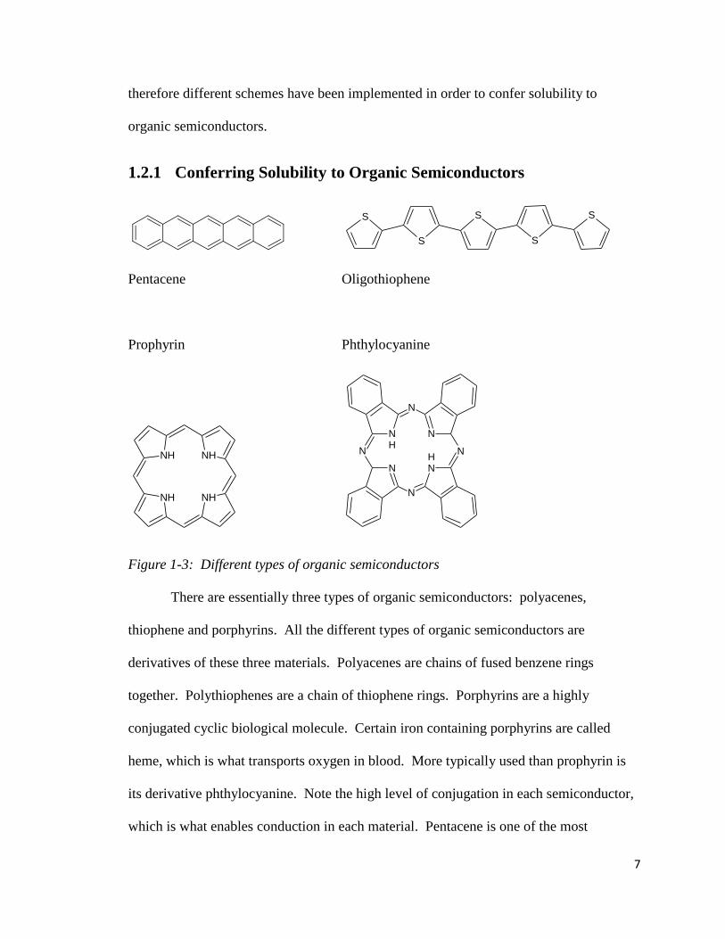
1.2.1 Conferring Solubility to Organic Semiconductors
Pentacene Oligothiophene
Prophyrin Phthylocyanine
Figure 1-3: Different types of organic semiconductors
There are essentially three types of organic semiconductors: polyacenes,
thiophene and porphyrins. All the different types of organic semiconductors are
derivatives of these three materials. Polyacenes are chains of fused benzene rings
together. Polythiophenes are a chain of thiophene rings. Porphyrins are a highly
conjugated cyclic biological molecule. Certain iron containing porphyrins are called
heme, which is what transports oxygen in blood. More typically used than prophyrin is
its derivative phthylocyanine. Note the high level of conjugation in each semiconductor,
which is what enables conduction in each material. Pentacene is one of the most
S
S
S
S
S
NH
NH
NH
NH
NH
N
N
N
N
N
NH
N

8
common and studied organic semiconductor because of its high mobility which is on par
with the mobility of amorphous silicon.15
The high mobility organic semiconductors that have been commonly cited to have
mobilities of over 1 cm2/Vs17 are usually small organic semiconducting molecules, which
need to be deposited through thermal evaporation and high vacuum. Some of these small
molecules are pentacene, oligothiophenes and single crystalline rubrene, which have been
shown to have mobilities ranging from 1-15 cm2/Vs.17 These materials are insoluble in
common solvents. It has been shown that some degree of solubility can be imparted to
these materials when placed in heated solvents.18 However, this is not conducive to spin
coating, drop casting, inkjet printing or gravure printing, as the solvent needs to be
maintained the high temperatures until after deposition.
The most common soluble organic semiconductors are polymeric systems, where
the polymer chains have been functionalized with side-chains in order impart solubility.
The trade-off is that the polymeric systems have much lower mobilities compared the
thermally evaporated small molecules, usually less than 0.1 cm2/Vs.19 The mobility
decrease is attributed to crystallinity and unordered packing as compared to small
molecules. Small molecules readily form crystalline structures through a very tight
herring-bone packing structure (figure 1.4). The tight packing of the small molecules
allows for a high degree of p-orbital overlapping between molecules, which increases the
mobility of the material. It is unfortunately for this reason, which also causes these
organic semiconductors to be insoluble in common solvents. It would be desirable to
impart solubility to small organic semiconducting molecules and maintain its tight

9
packing even after deposition. There have been many schemes to impart solubility to
these small molecules.
Figure 1-4: The tradition herring-bone structure of pentacene. Each line represents a
top down view of a single small organic semiconducting molecule.
1.2.1.1 Oligothiophenes Precursors
Different schemes have been implemented to improve the performance of the
oligothiophenes. There are schemes, which attempt to increase oxygen stability of the
semiconductor. Other schemes seek to the increase ordering of the molecules, thereby
increasing mobility. Of courses there are also schemes to allow oligothiophenes to
become dissolvable in common organic solvents for the possibility of solution processing
Oligothiophenes have been shown to have mobilities of 1.0 cm2/Vs,20 which is
lower than pentacene and rubrene, however oligothiophenes chemistry allows for highly
flexible addition of side chains, which may be favorable for tuning of solubility of
oligothiophenes. Figure 1.5 shows a molecule made by the Fréchet group,20-22 which
functionalizes polythiophenes by the addition of active ester groups on to the ends of the
oligothiophene. The ester groups with long chain alkanes impart solubility to the
oligothiophene groups, but through a thermolysis reaction, is removed and only the

10
oligothiophene is left.
Figure 1-5: Oligothiophenes have been modified with specific side chains to make them
soluble in organic solvents. The side chain can be removed with heat after deposition.
1.2.1.2 Soluble Pentacene
Since pentacene has shown high air stability, creation of a soluble pentacene has
always been highly desirable. Significant work has been focused on pentacene chemistry
in order to impart solubility to pentacene. Anthony’s group has have success in adding a
bulky side chain on to the middle ring of pentacene, which first serves to impart solubility
to pentacene (figure 1.6),23 it also changes the packing of molecule to go from the
traditional herring-bone structure to move to a face-to-face packing (figure 1.7). Using
this scheme, Anthony’s group has been able to achieve up to 1.0 cm2/Vs mobilites.
These are some of the highest reported mobilities for small organic semiconducting
molecules. This type of molecule unfortunately does not allow for multilayer solution
processing on top of the semiconductor, since the semiconductor can be dissolved if
another layer is printed on top of the existing semiconductor.
S
SS
S
S
O
CH3
O
Butyl
HexylO
CH3
O
Hexyl
Butyl
S
SS
S
S
CH3 CH3

11
Figure 1-6: Pentacene with TIPS side groups to allow for solubility and increased
ordering upon deposition
Figure 1-7: The packing of TIPS pentacene is no longer a traditional herring-bone
packing, but instead face to face packing.
1.2.1.3 Soluble Pentacene Precursors
Another way to impart to impart solubility to pentacene is to create a pentacene
precursor, similar in concept to the oligothiophene precursor. The basic concept of the
R
R
Si
CH3
CH3
CH3 CH3
CH3
CH3
Triisopropylsilyl
(TIPS)

12
precursor is to disrupt the conjugation within the pentacene by adding bulky groups to the
center ring of the pentacene. The bulky group breaks up conjugation within the
pentacene molecules, as well as disturbs p-orbital overlapping between molecules and
confers solubility through the bulky side chains. The first attempt at a pentacene
precursor, chemists added a chlorinated ring structure into the center ring of pentacene
ring (figure 1.8).24
Figure 1-8: The first soluble pentacene precursors
A more successful attempt was down by Afzali et al. from IBM, which added an
N-Sulfinylacetamide to the center ring through a Diels-Alder reaction (figure 1.9, 1.10).25
Mobilities were reported up to 0.8 cm2/Vs. The success of the pentacene precursor is that
after deposition pentacene is converted back to its original form and then is unaffected by
its bulky side chains, the original properties of pentacene is preserved. There have been
many other precursors which have followed this scheme.26-29
Figure 1-9: The concerted Diels-Alder reaction
Cl
Cl
Cl
Cl
Cl
Cl
Cl
Cl
+
CH2 CH2
CH2 CH2

13
Figure 1-10: The Diels-Alder reaction making pentacene soluble in organic solvents
The pentacene precursor from IBM (13,6-N-Sulfinylacetamidopentacene or SAP)
has been successfully used for fully printed organic TFT,30 showing mobilities in the
0.1cm2/Vs range. Beyond using this material for use into a printed TFT, little else has
been studied regarding this material. This thesis will deal with the thin film formation of
pentacene from the degradation of SAP.
1.3 Inorganic Nanoparticles
Up until this point only organic materials have been mentioned. However, it
would be incomplete to not at least briefly mention that there is also research being done
with inorganic materials to be used in printed electronics, mainly with synthesis of
inorganic nanoparticles.
The usage of inorganic materials is promising and should not be neglected
because the mobilities reported from inorganic materials TFTs are much higher than what
is has been seen with organic materials. Contrary to organic materials which have been
reported to be predominately p-type, n-type inorganic materials have been demonstrated.
. The reason for using nanoparticulate materials is for solubility. Inorganic
semiconducting crystals do not dissolve in common solvents. However, nanoparticles
can be encapsulated with functional groups which would allow for them to be dissolved
+
CH3
CH3
CH3O
O
N S O S
N
O
O
CH3
CH3
CH3
O
Pd2+ catalyst
CHCl3
1500C

14
in common solvents. Or additives can be added into solution in order stabilize
nanoparticles in order to form colloidal suspensions of the nanoparticles.
A second property of nanoparticles is the low melting or sintering temperature of
particles. Elemental nanoparticles have been found to have depressed melting
temperatures which are far below the bulk melting temperature, making incorporation of
these semiconductors on to plastics possible. By using a soluble semiconductor
nanoparticles, these nanoparticles can first be deposited through printing. The deposited
film probably would have low carrier mobility because of the small crystal size of
deposited film. However the film can then be heated in order to sinter nanoparticles.
After sintering of nanoparticles, the final crystal sizes of the semiconductors would grow
large enough to allow for decent conduction.
Early usage of nanoparticle semiconductors for printed electronics was done by
MIT media labs, where CdSe and CdTe were printed onto a substrate gated structure.31
Mobilities were reported to be approximately 1 cm2/Vs. A more recent used thiol
encapsulated ZnO and gave mobilites of 0.2 cm2/Vs.32 The use of ZnO was promising,
because first ZnO is a n-type material, which potentially can be coupled with p-type
organic materials to form CMOS. Also ZnO is transparent, which allows for ZnO to be
potentially incorporated into a display.
1.4 Organic Thin film Transistors
The TFT structure is the typical choice to creating organic transistors. Organic
semiconductors cannot easily be made into a mechanically stable substrate which
transistors can be built upon, as in silicon. Instead, transistors are built on top a
mechanically stable substrate such as glass or plastic and the organic semiconductor is

15
deposited and processed along with the other materials in the fabrication process. There
are different types of configurations which the OTFT can take, namely the bottom-gate
top contact OTFT, the bottom-gate bottom contact OTFT, the top-gate OTFT, substrate
gated bottom contact OTFT or substrate gated top contact OTFT.
As can be seen in figure 1.11, the top-gate OTFT is the most difficult to make.
The top gate OTFT requires a dielectric and metal gate to be processed on top of the
semiconductor. The organic semiconducting material is usually the most sensitive
material in an OTFT process, so it is always easier to deposit the organic semiconductor
last instead of first. For semiconductor material testing, the substrate-gated bottom
contact OTFT is the easiest to make and the most useful for testing. The whole OTFT
structure minus the semiconductor can be mass produced and stored before testing. Then
these substrates can then be used at a later time with a variety of different
semiconductors, which only needs to be deposited on top of the substrate to complete the
OTFT. One substrate can contain many devices with different W/L for testing, making
testing quick and the process highly repeatable. For the sake manufacturing simplicity
and testing, all OTFTs used in these studies were substrate gated bottom contact OTFTs.

16
Figure 1-11: Different OTFT configurations
1.4.1 Operation of OTFTs
Due to the presence of traps caused by disorder in organic semiconductors it is
difficult for organic semiconductors to become depleted. Therefore, OTFTs are run in
accumulation mode. A negative bias is placed on the gate electrode. The negative bias
attracts positive carriers of the, generally p-type, semiconductor to form on the
semiconductor to dielectric interface creating a channel between the source and drain
electrode, allowing conduction to occur between the source and the drain (figure 1.11).

17
Figure 1-12: Operation of a p-OTFT
If stronger negative bias is placed on the gate electrode more holes are gathered to the
dielectric/semiconductor interface allowing for more conduction. Figure 1.12 shows the
I-V characteristics of a typical OTFT. The shape generally looks similar to what is seen
in a typical single crystalline silicon MOSFET. Hence, the square-law (equation 1.1)
which describes typical silicon MOSFETs is also used to describe an OTFT.

18
Figure 1-13: IV Characteristics of a typical OTFT. (top) Output characteristics and
(bottom) transfer characteristics of a pentacene OTFT with1000Å of oxide (W/L =
125µm/15 µm).
2)(2
)2
(
TGSOXDS
DSDS
TGSOXDS
VVCL
WI
VV
VVCL
WI
Equation 1-1: Square-law equations for triode (top) and saturation (bottom).
-8.E-06
-7.E-06
-6.E-06
-5.E-06
-4.E-06
-3.E-06
-2.E-06
-1.E-06
0.E+00
-40.00-30.00-20.00-10.000.00
ID[A
]
VD [V]
VG= -40V
VG= -30V
VG= -20V
VG= -10V
VG= 0V
1.E-08
1.E-07
1.E-06
1.E-05
1.E-04
-40-30-20-10010
ID[A
]
VG [V]
VD= -10V
VD= -40V

19
1.4.2 Transport in OTFTs
Even though OTFTs apparently functions in the same manner as a bulk silicon
MOSFET, however, this is only a model. Carrier transport in an organic semiconductor
is quite different than in single crystalline silicon. Organic semiconductors are generally
polycrystalline or amorphous, these highly disordered systems have many implications
which are not found in single crystalline silicon. In the next sections, the origin of
conduction inorganic semiconductors is describe and the effects of disorder on
conduction is discussed.
1.4.2.1 Conduction in organic materials
Conduction occurs in metals because of metallic bonding because there is a “sea”
of delocalized electrons. These delocalized electrons are not strongly bound to any
particular atom, hence can moved around allowing for conduction. Metallic bonding is
usually contrasted with covalent bonding where electrons forming the bonds are spatially
fixed and are not capable of long range movements.
In inorganic semiconductors, taking silicon as an example, silicon atoms interact
with each other through covalent bonding. Specifically the bonding is bonding of sp3
hybridized orbital. Conduction in silicon is also difficult, however by the usage of
dopants, conduction can be increased. Dopants, are merely impurities which when added
into the semiconductor is able to introduce weakly bound electrons and hence are
delocalized in the silicon crystal lattice. With dopants, conduction is made easier,
because just like in the case of the metallic bond, there is now a sea of delocalized
electron in which conduction can take place.

20
In order for conduction to occur in organic materials, there needs to be
delocalized electrons in the organic material. This can be done within a single molecule
through bonds and conjugations. When a carbon atom is sp2 hybridized, the three sp
2
orbitals form directional bonds with neighboring atoms. The remaining p-orbital,
usually form a -bond with a neighboring p-orbital. When two carbons interact through a
-bond and a -bond bond, this called a double bond. Whereas the electrons involved in
the -bond are fixed in location, the -bond electrons are able to interact with
neighboring -bonds. Therefore, if a molecule has a chain of interacting -bonds, then,
within that molecule, the electrons in the -bonds are delocalized; this is called
conjugations. Conjugation allows for electrons to move beyond its -bond and move a
longer distance, conjugation also gives added stability to the molecules through
resonance.
Figure 1-14: The left shows a simple alkadiene in its usually line representation. On the
right the same molecule is shown with the π-bond specifically drawn showing the
interaction of the p-orbitals
Now for transport of electrons between organic molecules occurs by -bond
overlapping between molecules. In an organic crystal, molecules are held together by
van der Waals forces, or more specifically, London dispersion forces.33 These
interactions are relatively weak and therefore distances between molecules are relatively
CH2
CH3
CH3
CH3

21
large. Lattice spacing is much large for organic crystals and bandgaps in organic
semiconductors are also relatively large. Conduction in organic molecules is thereby
much lower than in inorganic semiconductors. If, the intermolecular distances can be
forced together more closely, bandgaps can be reduced, carriers can travel from molecule
to molecule easier and conduction can also be increased.
The origin of bandgaps in organic materials comes from the interactions of
HOMO/LUMO levels of each individual molecule.34 The HOMO (highest occupied
molecular orbital) is usually analogous to the valence band in inorganic semiconductors.
The LUMO (lowest unoccupied molecular orbital) is analogous to the conduction band of
inorganic semiconductors. The energy difference between the HOMO/LUMO levels is
the definition of the band gap for an organic semiconductor. When multiple
HOMO/LUMO levels interact, a continuum is formed becoming the energy bands for
organic semiconductors.
1.4.2.2 Multiple Trap and Release (MTR)
A defining feature of organic crystals is the lack of covalent bonds between
organic molecules. In inorganic systems the crystal is held together tightly with covalent
bonds, keeping lattice points close together and keeping crystals relatively well order, all
resulting in high mobility. Organic crystals are held together with van der Waals forces,
keeping molecules far apart and crystals are highly susceptible to crystal defects.
Organic crystals are generally polycrystalline; crystal boundaries also imperfections and
are considered defects.
These crystal defects lead to localized energy perturbation and form traps states.
These traps greatly effect the ability for carriers to travel through the semiconductor film.

22
Two effects of these trapped states is, thermally activated transport and field dependent
mobility.
There are many models which try to describe the effect of traps on the TFT
mobility in semiconductors. One prevalent model is the multiple trap and release model
(MTR). MTR was first used to describe transport in hydrogenated amorphous silicon
TFTs35 and now it has been adapted to describe OTFTs.
The following discussion of MTR is taken from Merlo et al.36 In MTR the traps
originating from both grain boundaries as well as internal crystalline defects are assumed
to be distribution of trap states is to assume that the states both from grain boundaries and
internal crystal defects are uniformly distributed throughout the semiconductor film. The
trap states are assumed to be in an exponential distribution of states in the band gap.
Most carriers are trapped in the exponential trap states. When carriers are trapped
they have no mobility and thereby are unable to move. When carriers are freed from the
traps, these free carriers are then able to move around. In short, carriers generally are
trapped in shallow traps and through thermal perturbation carriers may be release, but
then trapped again by another trap, hence the name multiple trap and release.
MTR states that the effective mobility (μeff) is related to the free carrier mobility
(μ0) and the ratio of free holes (NV) and total induced holes (NV + NT) by by the
following relationships shown in equation 1.2.

23
Tk
E
Tk
EE
N
N
Tk
EENN
Tk
EENN
N
NNN
N
B
A
B
VF
V
T
eff
B
FT
TT
B
VF
VV
T
VTV
V
eff
exp
exp1
1
exp
exp
1
0
0
0
0
0
0
0
0
Equation 1-2: MTR equations
Here NV is the aerial density of free holes and NT is the aerial density of trapped
holes. NV0 and NT0 are the effective density of free and trapped states respectively, kB is
the Boltzmann constant, Ef is the Fermi level and Ev is the valence band edge. The
results show that the effective mobility can be approximated with an Arrhenius
relationship with an activation energy EA. The activation energy is the energy necessary
to release trapped carriers. Of course the trap depth is not a discrete value, but instead an
exponential distribution.
From the Arrhenius equation it is very clear that the mobility is thermally
activated. As temperature is increased more carriers are “activated” increasing the
effective mobility, which increases the current of a TFT. A physical explanation states
that as temperature is increased, the trapped carrier gain enough energy to leave traps to
become free. This causes the ratio of free to trapped carrier increases, so the effective
mobility also increases.
The less apparent effect which can be seen in the MTR equation is electric field
induced mobility. As gate electric field is increased, the activation energy is also

24
decreased. The activation energy is the difference between the Fermi level and the
valence band edge. Increasing the gate electric field moves the Fermi level closer to the
valence band edge, effectively decreasing activation energy. Physically, moving the
Fermi level is equivalent to filling traps making the exponential trap distribution more
shallow, which allows carriers to be freed more easily.
Both these effects have been observed experimentally. As a result the extraction
of mobility from OTFTs is extremely difficult. The extraction of mobility will be
covered in more detail in the next chapter.
1.5 Organization
This thesis deals with the processing of the IBM pentacene precursor in order for
use in printed electronics. Even though it has already been used an tested as printable
materials with relatively high performance, however the mechanism of thin film
formation is unknown. The rest of this thesis describes experiments which deduce the
film formation mechanism of the IBM precursor.
Chapter 2 goes through the details of manufacturing and testing a pentacene
transistor. All the fabrication steps are specifically for a substrate gated TFT. Testing
details are given for electrically probing the TFT and extracting the mobility and on/off
ratio. Then details are given for using AFM, SEM and GIXD in order to test the
semiconducting material. The descriptions of AFM, SEM and GIXD are given
specifically for the measurements to be used throughout this thesis.
Chapter 3 begins looking at the chemistry of the pentacene precursor with UV-
vis. The reaction rate and activation energy is extracted, and simple conclusions are

25
drawn about the solid-state degradation reaction. This knowledge allows for further
study of pentacene thin film growth.
While chapter 3 only looks at the reaction rate of the pentacene precursor forming
a thin film, chapter 4 looks into the details of the solid-state reaction of the precursor
transforming into pentacene with amorphous SiO2 as the substrate. Oxide will not be
used as a material in printed electronics, however it still the most common material used
for TFT testing. The growth of pentacene through evaporation on oxide is well studied,
therefore serves as a model for the growth of pentacene through a precursor. The purpose
of this chapter is to understand how this material converts from the precursor form into a
thin film of pentacene. This knowledge aids in the understanding of tuning the pentacene
precursor for usage in transistors. The reaction is traced using SEM, AFM and GIXD.
Specifically, temperature dependence of nucleation density, mechanism of crystal
growth, surface topology and crystal size are described.
Chapter 5 goes on to look at pentacene films formation on five different
substrates. These substrates are all materials which are useful in organic semiconductor.
This chapter is similar to chapter 4, however moves away from oxide as the substrate to
grow pentacene. Understanding how pentacene grows on these other substrates is
imperative for printed electronics. The growth of pentacene thin films on each substrate
is compared and contrasted with each other. This also gives further insight on the growth
of thin-films through a precursor system.
Chapter 6, the pentacene precursor is subject to different heat-treatments in order
to improve TFT performance. To date, the processing of precursor systems has been
limited to only one temperature. This chapter explores the processing of the pentacene

26
precursor using two temperature heating steps. Two temperature processing promises to
create higher performance TFTs than single TFTs processed at a single temperature. The
microstructure of the pentacene thin films made using two temperature processing is
compared with thin films made with the traditional one step processing. TFTs fabricated
with this method are also compare with TFTs fabricated using the tradition processing.
This chapter shows that using different heat-treatments can tune the performance of a
semiconductor formed from a precursor system.
Finally, chapter 7 summarizes the results in this thesis and give suggestions for
future work.

27
1.6 References
1. Lovinger, A. & Rothberg, L. Electrically active organic and polymeric materials for
thin-film-transistor technologies. JOURNAL OF MATERIALS RESEARCH 11, 1581-
1592(1996).
2. Liao, F., Chen, C. & Subramanian, V. Organic TFTs as gas sensors for electronic
nose applications. SENSORS AND ACTUATORS B-CHEMICAL 107, 849-855(2005).
3. Steudel, S. et al. Comparison of organic diode structures regarding high-frequency
rectification behavior in radio-frequency identification tags. JOURNAL OF
APPLIED PHYSICS 99, (2006).
4. Lee, J. & Subramanian, V. Weave patterned organic transistors on fiber for e-textiles.
IEEE TRANSACTIONS ON ELECTRON DEVICES 52, 269-275(2005).
5. Read, S.F.J. Dynamic Nuclear Polarization in a Perylene---Iodine Complex. J. Chem.
Phys. 36, 3098-3099(1962).
6. Shoda, T. et al. Molecular packing analysis of benzene crystals. Part 2. Prediction of
experimental crystal structure polymorphs at low and high pressure. Journal of
Molecular Structure: THEOCHEM 333, 267-274(1995).
7. McNeill, R. et al. Electronic Conduction in Polymers. I. The Chemical Structure of
Polypyrrole. Australian Journal of Chemistry 16, 1056-1075(1963).
8. Bolto, B. & Weiss, D. Electronic Conduction in Polymers. II. The Electrochemical
Reduction of Polypyrrole at Controlled Potential. Australian Journal of Chemistry
16, 1076-1089(1963).

28
9. Bolto, B., McNeill, R. & Weiss, D. Electronic Conduction in Polymers. III.
Electronic Properties of Polypyrrole. Australian Journal of Chemistry 16, 1090-
1103(1963).
10. Shirakawa, H. et al. Synthesis of electrically conducting organic polymers: halogen
derivatives of polyacetylene, (CH)x. J. Chem. Soc., Chem. Commun. 578-580(1977).
11. McGinness, J., Corry, P. & Proctor, P. Amorphous semiconductor switching in
melanins. Science 183, 853-5(1974).
12. Tsumura, A., Koezuka, H. & Ando, T. Macromolecular electronic device: Field-
effect transistor with a polythiophene thin film. Appl. Phys. Lett. 49, 1210-
1212(1986).
13. Blochwitz, J. et al. Low voltage organic light emitting diodes featuring doped
phthalocyanine as hole transport material. Appl. Phys. Lett. 73, 729-731(1998).
14. Tang, C.W. & VanSlyke, S.A. Organic electroluminescent diodes. Appl. Phys. Lett.
51, 913-915(1987).
15. Lin, Y. et al. Stacked pentacene layer organic thin-film transistors with improved
characteristics. Electron Device Letters, IEEE 18, 606-608(1997).
16. Kline, R.J. et al. Significant dependence of morphology and charge carrier mobility
on substrate surface chemistry in high performance polythiophene semiconductor
films. Appl. Phys. Lett. 90, 062117-3(2007).
17. Kelley, T.W. et al. Recent Progress in Organic Electronics: Materials, Devices, and
Processes. Chemistry of Materials 16, 4413-4422(2004).
18. Tao, C. et al. Solution processed pentacene thin films and their structural properties.
Materials Science and Engineering: B 140, 1-4(2007).

29
19. Chang, J. et al. Enhanced Mobility of Poly(3-hexylthiophene) Transistors by Spin-
Coating from High-Boiling-Point Solvents. Chemistry of Materials 16, 4772-
4776(2004).
20. Murphy, A.R. et al. Organic Thin Film Transistors from a Soluble Oligothiophene
Derivative Containing Thermally Removable Solubilizing Groups. Journal of the
American Chemical Society 126, 1596-1597(2004).
21. Murphy, A.R. et al. Self-Assembly, Molecular Ordering, and Charge Mobility in
Solution-Processed Ultrathin Oligothiophene Films. Chemistry of Materials 17,
6033-6041(2005).
22. Chang, P.C. et al. Film Morphology and Thin Film Transistor Performance of
Solution-Processed Oligothiophenes. Chemistry of Materials 16, 4783-4789(2004).
23. Sheraw, C. et al. Functionalized Pentacene Active Layer Organic Thin-Film
Transistors. Advanced Materials 15, 2009-2011(2003).
24. Brown, A.R. et al. Precursor route pentacene metal-insulator-semiconductor field-
effect transistors. J. Appl. Phys. 79, 2136-2138(1996).
25. Afzali, A., Dimitrakopoulos, C. & Breen, T. High-performance, solution-processed
organic thin film transistors from a novel pentacene precursor. JOURNAL OF THE
AMERICAN CHEMICAL SOCIETY 124, 8812-8813(2002).
26. Weidkamp, K.P. et al. A Photopatternable Pentacene Precursor for Use in Organic
Thin-Film Transistors. Journal of the American Chemical Society 126, 12740-
12741(2004).

30
27. Afzali, A., Dimitrakopoulos, C. & Graham, T. Photosensitive pentacene precursor:
Synthesis, photothermal patterning, and application in thin-film transistors.
ADVANCED MATERIALS 15, 2066-+(2003).
28. Afzali, A., Kagan, C. & Traub, G. N-sulfinylcarbamate-pentacene adduct: A novel
pentacene precursor soluble in alcohols. Synthetic Metals 155, 490-494(2005).
29. Okamoto, K. et al. Synthesis and thermolysis of Diels-Alder adducts of 2,9-
dialkylpentacenes with diethyl azodicarboxylate. Journal of Physical Organic
Chemistry 21, 257-262(2008).
30. Molesa, S. et al. A high-performance all-inkjetted organic transistor technology.
Electron Devices Meeting, 2004. IEDM Technical Digest. IEEE International 1072-
1074(2004).doi:10.1109/IEDM.2004.1419384
31. Ridley, B.A., Nivi, B. & Jacobson, J.M. All-Inorganic Field Effect Transistors
Fabricated by Printing. Science 286, 746-749(1999).
32. Volkman, S. et al. A novel transparent air-stable printable n-type semiconductor
technology using ZnO nanoparticles. Electron Devices Meeting, 2004. IEDM
Technical Digest. IEEE International 769-772(2004).
33. Li, L., Meller, G. & Kosina, H. Carrier concentration dependence of the mobility in
organic semiconductors. Synthetic Metals 157, 243-246(2007).
34. Elandaloussi, E.H. et al. Effect of Chain Extension on the Electrochemical and
Electronic Properties of π-Conjugated Soluble Thienylenevinylene Oligomers.
Journal of the American Chemical Society 119, 10774-10784(1997).
35. Schiff, E.A. Trap-controlled dispersive transport and exponential band tails in
amorphous silicon. Phys. Rev. B 24, 6189(1981).

31
36. Merlo, J.A. & Frisbie, C.D. Field Effect Transport and Trapping in Regioregular
Polythiophene Nanofibers. The Journal of Physical Chemistry B 108, 19169-
19179(2004).

32
2 Experimental Methods and Characterization
Techniques
Since this thesis is primarily concerned with solution processed pentacene for
organic TFTs, this chapter shows all the steps used in fabricating and characterizing an
OTFT. The first part of the chapter deals with the fabrication and the choice of
fabrication steps to make the standard OTFT that will be used in this thesis. Then, all of
the different characterization techniques which will be used in this thesis will also be
described and explained. The characterization techniques used are, extraction of mobility
from OTFT IV curves, SEM for monitoring semiconductor thin-film formation, AFM for
looking at semiconductor thin-film topology and GIXD for deducing crystal structure of
thin-films. Finally, a section will be given to UV-vis and analyzing UV-vis data.
2.1 OTFT Fabrication and Testing
2.1.1 OTFT Fabrication
OTFT substrates were 4” heavily doped n-type wafers. The gate oxide was grown
by wet oxidation at 9000C and grown to a thickness of 1000Å. The substrate gated OTFT
structure is merely a test structure to test semiconducting materials. The thickness of the
gate oxide was chosen to mimic the vertical electrical fields which may be used in a fully
printed device.

33
The oxidized wafers are then heated to 1200C to drive off any water vapor on the
oxide, and then placed in HMDS vapor. The HMDS vapor forms a monolayer of HMDS
onto the oxide surface which would promote adhesion of photoresist to the oxide surface.
After the deposition of HMDS, positive photoresist is spun on using the standard
UC Berkeley microlab process, along with a soft bake of the photoresist. The wafer is
patterned through a stepper, which patterns 64 identical dies onto the wafer. Each die
contains patterns for OTFT source drain pads defining various W/L ratios. The patterned
wafers are developed using the standard process and then hard baked.
Finally, the source/drain pads made by thermally evaporated gold with a chrome
adhesion layer. Evaporation was done at a base pressure of approximately 5×10⁻⁷
torr.
The thicknesses of the two metal layers are 500Å of gold and 15Å of chrome, with a rate
of 5Å/s and 1Å/s respectively. Lastly the source/drain pads are finally formed by lift off.
This is done by placing the wafer into acetone, where all the photoresist and excess gold
is removed. The only gold left are the gold which was deposited onto the oxide from the
patterned photoresist. Figure 2.1 and figure 2.2 describe the full process.

34
Figure 2-1: Substrate-gated TFT process
Figure 2-2: Cross-section view of the substrate-gated OTFT process
Because these wafers are many times made in advanced much before
semiconducting material will be deposited, there is fear that the wafers may have
collected contaminants. Therefore before depositing semiconducting materials, the wafer
is cleaned using step 1 of an RCA clean. Step 1 of the RCA clean is a wafer soaks in
H20:NH4OH:H2O2, 5:1:1. This removes all organic contaminants that may have
accumulated from the liftoff process and storage. Once again, the wafer is baked dry and

35
HMDS is redeposited. This time HMDS is applied to help the ordering of organic
semiconductors which will be grown on the oxide surface. The reapplication of HMDS
is to ensure that HMDS has not been removed by the processing steps between the first
HMDS application and the deposition of organic semiconductors. Generally, if it is
desired to remove HMDS from oxide surfaces, oxide wafers are placed in oxygen
plasma. Even though wafers have not been subjected to plasma treatments, the
application of HMDS is simple enough that this extra step was added to ensure that
HMDS is still on the oxide surface. At this point semiconducting material can now be
deposited through spin, inkjet printing or evaporation, on top of the processed wafer to
form a completed TFT.
2.1.2 Electrical testing of OTFT
Electrical testing was done using by probing with a Rucker & Koll probe station
under an inert nitrogen ambient in conjunction with an Agilent 4156C parametric
analyzer. The gate contact was made by using the probe station chuck contacting the
heavily doped substrate. Contacting the source and drain was done by scratching through
the semiconducting material as shown in figure 2.3.
Figure 2-3: Contacting source/drain pads on TFTs
In order to reduce gate leakage, each devices was isolated from the others by
scratching the semiconducting material around each device. The standard testing

36
conditions swept Vds from 10V to -40V and step Vgs to -40V. All testing was done under
nitrogen ambient.
2.1.3 Mobility extraction
One of the most important benchmarks of an OTFT performance is mobility.
This however is also one of the most problematic parameters to extract. The IV
characteristic of an OTFT visually looks similar to that of a traditional MOS, therefore
the square-law is used to model electrical behavior of the OTFT.
The square law however, fails to model the nonidealities which are significant in
OTFT. Issues of at the contacts such as, contact resistance, Schottky barriers, carrier
injection are not modeled into the square law. Other issues which are unique to OTFT,
such as gate-bias dependent mobility,1-3
thermally activated transport1 and ill-defined turn
on characteristics4,5
cannot be addressed using standard MOS equations.
2)(2
)2
(
TGSOXDS
DSDS
TGSOXDS
VVCL
WI
VV
VVCL
WI
Equation 2-1: Square-law equations for triode (top) and saturation (bottom).
Judging from all the aforementioned problems finding the mobility of an OTFT is
problematic. Using the standard square-law approach, all the contact effects would be
convoluted in the mobility extraction. Even if the contact effects can be removed,
knowledge of the threshold voltage is necessary before mobility can be properly
extracted.
In OTFTs the threshold voltage is ill-defined, because turn on is gradual. The
semiconductor changes from nonconducting to conducting as carriers accumulate and

37
traps are filled by increasing the electric field over the gate. As more traps are filled,
more carriers are available for conduction. Due to this gradual turning of OTFTs, it is
difficult to define a specific threshold voltage on OTFTs.
Equation 2.2 and 2.3 shows a way to extract mobility using the slope of the
transfer curve and eliminates VT dependency and assumes no gate voltage dependency.
DSox
m
DSOXm
TGSOX
GS
DSm
ICL
W
g
ICL
Wg
VVCL
W
V
Ig
2
2
)(
2
Equation 2-2: Mobility in saturation
DSox
m
DSOX
GS
DSm
VCL
W
g
VCL
W
V
Ig
Equation 2-3: Mobility in triode
In this equation, the mobility is extracted from the gm of the transistor. Due to the slow
turning of the transistor, the number carriers for conduction as well as the mobility is
clearly gate voltage dependent.6-11
As a stronger field is place on the gate (more negative
voltage), the mobility of holes increase. At extremely high voltages, the mobility has
been shown to start decreasing.3 In practice most of these effects are neglected and, only
the highest saturation mobility is reported.12

38
2.2 Scanning Electron Microscopy (SEM)
Scanning electron microscopy was invented in the 1930s.13
Scanning electron
microscopy is one type of electron microscopy where an electron beam scanned across
the surface of the sample in a raster scan pattern. The incident bean interacts with the
sample and knocks off electrons from the sample and collected by the detector to form
the image. Due to the electron interaction with the atoms, information can be extracted
about composition, topology and electrical conduction. SEM allow for many high
magnification images to be visualized quickly.
In this thesis, visualization of semiconducting films was predominantly done
using SEM due to the simplicity and speed of this technique. The LEO 1550 was the
SEM used. The base pressure of the main SEM chamber is kept below 2×10⁻⁵
torr, and
the gun is kept below 1×10⁻⁸
torr. Because organic semiconducting materials are easily
destroyed by high energy, the beam energy was always kept below 5kV. Even so, after
long use on a single region of a sample, clear “burn” marks are seen. SEM samples were
always deposited on oxidized test wafer. Before deposition of samples step 1 of the RCA
clean was to clean the substrates.
In this thesis SEM was used predominately for three purposes. First, SEM was
utilized to “look” at growing film of pentacene inorder to gain a qualitative understanding
for pentacene film formation from a precursor. Second, SEM enabled the nucleation
density of growing pentacene crystals to be counted and quantified. The sizes of
pentacene crystalline structures are also measured. Lastly, since the electron beam
interacts with the pentacene and substrate differently, the wetting and dewetting of
pentacene films on substrates can be measured.

39
SEM pictures are saved in the uncompressed TIFF format. Therefore images can
be opened and analyzed with any image processing program. The open-source software
The Gimp was used to analyze all the images from SEM. Nucleation site were counted
up by hand from the SEM images. The dewetting of films was found by using the
threshold feature in The GIMP which creates binary images showing the substrate as a
white color and pentacene films as black. The percent coverage of pentacene film is then
measured by THE GIMP.
Figure 2-4: Example of SEM image to for counting pentacene nucleation sites. The
black square shows an example of sample damage caused by the electron beam from
zooming into particular regions.

40
Figure 2-5: (above) A regular SEM image before thresholding. (below) A processed
SEM image after thresholding, with black areas indicating pentacene and white areas
indicating exposed substrate.

41
2.3 Atomic Force Microscopy (AFM)
The precursor to the AFM was the scanning tunneling microscope (STM). The
STM allowed for high resolution images of conductive material. AFM was invented
1986,14
which combined the STM with surface profiler. The profiler is a tip with a small
mass, which deflects as it moves across the surface. Due to the small mass of the tip, the
sample will not be destroyed by the scanning action. By monitoring the deflection of the
tip, the surface profile of the sample can be taken. AFM has the benefit of being able to
scan a 2-D area much like SEM, but true 3-D information is given.
An AFM probe is a cantilever with a sharp micromachined tip attached to the end
of the cantilever. The vertical height of the tip is measured by a laser and photodiode.
As the tip is rastered across the surface of a sample the vertical deflection of the tip
translates into topological image of the sample. There are two main modes of AFM
operation, contact and tapping mode. In contact mode, the tip is scanned across the
surface of the sample in constant contact with the sample surface. This has the
disadvantage of the probe potentially sticking to samples, especially from water adhesion.
Also for extremely soft samples contact mode AFM can potentially damage samples.

42
Figure 2-6: A typical AFM tip setup
Tapping mode AFM was invented counter these problems. In tapping mode, the
tip vibrates and taps the surface of the sample as the tip scans across the surface. The tip
made to resonate/vibrate a fixed frequency and amplitude, creating the “tapping.” As the
tip rasters across samples the amplitude of the tip changes due to the different features on
the sample, which translates to height changes.
The AFM used in these studies was a DI Dimension 3100 AFM. AFM was used
to visualize the surface topology on a select few SEM samples where more data was
needed. Due to the large number of SEM samples made and the tedium and slow
scanning speeds of AFM not all SEM samples were scanned by AFM. Since organic
materials are relatively soft, it was found that contact mode AFM was destructive to these
samples. All samples, therefore, were scanned in tapping mode. Tap300 tapping mode

43
tips were purchased from Ted Pella, Inc. The tapping frequency of the tip is
approximately 300kHz. The same samples used for SEM were also used for AFM.
For each scan, scanning parameters were adjusted in order to obtain the best
images. Parameters adjusted were, scan speed, scan size, lines per sample and
amplitudes. Due to the softness of pentacene films it was found that a slow scan rate
produced the best images. For images with large roughness, slow scans were imperative
inorder for even a reasonable image to be produced. It is due to this reason that SEM was
the predominate method of characterizing films. Even though AFM is able to give a true
3-D image, however images are limited to a size of 30×30µm at most, and each image
require up to a 20 minute scan.
Data extracted from AFM were analyzed with the open-source software
Gwiddyon. For each image, line and plane fitting were performed to normalize the
background. AFM was specifically used measure the profiles of cross-sections of images
and to find the rms roughness of films.

44
Figure 2-7: AFM image analyzing the profile of a cross-section
2.4 Glancing Angle X-ray Diffraction (GIXD)
X-ray diffraction is used in the thesis in order to deduce the crystal structure of
organic semiconducting films. It was developed by William L. Bragg and William H.
Bragg, which they were awarded the Nobel Prize.15
Their discovery can be readily
summarized by the famous Bragg’s Law:
nd )2sin(2
Equation 2-4: Bragg’s Law

45
In the equation (equation 2.4), n is an integer, is the wavelength of the X-ray, d is the
interplanar spacing of the crystal, and is the angle between the incident X-ray and the
scattering plane. This equation describes the conditions for constructive interference of
X-rays, given the angle of the incident X-ray. The generated X-ray diffraction pattern
gives the reciprocal lattice of a sample, which is useful to deducing the crystal structure.
Tradition X-ray diffraction on organic materials becomes more problematic
because of the weak signals which arise from organic materials and relatively close peaks
due to the large inter-plane spacing. Glancing angle X-ray diffraction with a synchrotron
source serves to solve these problems.
Figure 2-8: Schematic of GIXD setup
GIXD uses an extremely low incident angle (approximately 0.10-0.2
0). This
limits the amount of X-rays which penetrate the sample, so that the substrate would not
interfere with the data of the organic material, therefore the background noise is reduced.
Another benefit of the GIXD setup is that crystalline monolayers can be visualized,

46
where in the traditional setup it cannot. Finally, a synchrotron X-ray source, because the
source is brighter and the bandwidth is more narrow, allowing for higher resolutions and
stronger diffraction signals.
All GIXD experiments were done at the Stanford Synchrotron Radiation
Lightsource on the 11-2 and the 7-2 beamline. The 11-2 beamline gives low resolution 2-
D diffraction pattern of the analyzed samples. The 7-2 beamline gives high resolution 1-
D xray diffractions. This beamline was specifically used to look at the 100 peak of
pentacene in order to estimate crystal size. Diffraction patterns were used to deduce three
attributes of the samples; film texturing, pentacene morphotypes and relative crystal size.
Texturing can be found by looking at arcing in the in-plane peaks as well as the mixed
reflections.
Figure 2-9: (left) GIXD of pentacene film processed at 1600C. (right) GIXD of
pentacene film processed at 1250C. In the boxed in-plate peak, from bottom up the
identity of the peaks are 100, 200, and 300 respectively.

47
In the GIXD pattern showing the pentacene film processed at 1600C in figure 2.9,
the in-plane reflections and the mixed reflections are boxed. The in-plane reflections are
the same are the reflections seen in regular X-ray diffraction. The out-of-plane
reflections are on the x-axis, but are blocked off, because of the beam stop. The mixed
reflections are the linear combination of both the in-plane and out-of-plane reflections.
There are two ways to look at texturing using the 2-D diffraction patterns.
The first way to look for texturing is to look at the “arcing” in the 100 plane. In a
completely disordered polycrystalline film, such as a powder film, distinct peaks will not
be seen. Instead “rings” are seen. These rings come from the superposition of identical
diffraction patterns rotated at many different angles. As texturing increases and the
randomness of crystals decreases, the “rings” shorten into arcs. When crystals are well
ordered, then the arcs turn into distinct spots. Therefore by looking at the length of arcs,
the texturing of films can be determined, with longer arcs showing high disorder, a full
ring indicates no ordering at all, and a isolated point shows perfect ordering. From figure
2.10, the 100 “arc” from a film processed at 1250C is much larger than the 100 “arc” on a
film processed at 1600C, indicating no low order for film processed at 125
0C and higher
order for films processed at 1600C.

48
Figure 2-10: (Left) The location of the 100 plane is shown. (Top right) The 100 plane
from a film processed at 1250C. (Bottom right) The 100 plane from a film processed at
1600C.
The second way to look at texturing is to look for mixed reflections. When mixed
reflections become distinct, that is a good indication of texturing. In disordered
polycrystalline samples where diffraction rings are seen, the rings are a blur of all
diffraction peaks, both in-plane out-of-plane as well as mixed reflections. When the rings
resolve into distinct peaks, blur on the mixed reflection also resolves and is no longer
mixed in with the in-plane andn out-of-plane reflections. The film processed at 1250C
does not have any distinct mixed reflections showing poor texturing.

49
There are three morphotypes of pentacene. This is discussed in further detail in
chapter 4. The three morphotypes are an orthorhombic monlayer phase,16
a triclinic thin-
film phase17
and triclinic bluk-like phase.17
The existence of different morphotypes of pentacene can be found by looking for
doubling of peaks. Both the thin-film phase and the bulk-phase in pentacene have a
triclinic crystal structure, however they have different lattice constants. Therefore, if
there are two peaks that show up close to each other, this is highly indicative that there
are two morphotypes of pentacene present. In figure 2.11, it can be seen that the film
processed at 1600C has two morphtypes of pentacene present while the film at 125
0C
does not. The monolayer phase needs more complex methods in order to be identified, so
it cannot be determined whether or not it exists. It is assumed that it does not exist,
because the monolayer phase needs persists only under specific conditions which the
pentacene precursor does not have.
Figure 2-11: (Left) A film processed at 1250C does not show a double peak. (Right) The
A film processed at 1600C shows a double 300 peak.

50
Finally, crystallite size is extracted by measuring the full width half maximum of
the 100 peak and applying the Debye-Scherer formula. The wider the peak, the smaller
the crystallite size. All of the crystallite sizes were extracted using a high resolution X-
ray rocking curve, rocked around the 100 plane. Qualitatively, by looking at peak width,
a quick comparison of crystal size can be made. Looking back at figure 2.10, the 100
peak at 1250C is extremely narrow, showing a large crystal compared to the 160
0C film.
Only the relative crystal size of the pentacene can be compared, because when extracting
the crystal sizes, for simplicity the crystals were assumed to have a cubic crystal
structure.
2.5 UV-vis Spectroscopy
Figure 2-12: Diagram of Beer-Lambert absorption of an incident beam.
From the name UV-vis spectroscopy, it can be inferred that this method measures
the interaction of light ranging from UV wavelengths to visible wavelength with a
sample. With UV-vis spectroscopy, the measurement can either be absorbance or

51
transmission of the light at different wavelength. In the study of UV-vis spectroscopy in
chapter 3, only absorbance data is used. The use of absorbance is the most typical
method for used in UV-vis spectroscopy. UV-vis has with most light spectroscopic
techniques operates by Beer-Lambert law.
Beer-Lambert law is the empirical relationship which describes how light is
absorbed through a material. This is the principle which data from UV-vis spectroscopy
is interpreted. The equation is:
Alc
I
I 10100
Equation 2-5: Beer-Lambert equation
So the absorbance, A, is related to l, the length of the sample, c the concentration
of the chemical, and the extinction coefficient. In an UV-vis absorption spectrum, A is
plot for different wavelengths of light. For every chemical which absorbs light from the
UV to visible light range, a unique pattern of absorption is seen, and can be used to
identify the chemical.
Usually samples are soluble in a solvent, and the chemicals are place in a cuvette
with a fixed size. Assume now that there are two chemicals in the cuvette. The
absorbance, A, is affected by both chemicals and the absorbance is now:
2211 lclcA
Equation 2-6: Absorbance when there are two chemicals
The length are identical for both chemicals, because the size of the cuvette is fixed and
both chemicals are dispersed in the cuvette.

52
Supposed there is a chemical reaction where AB. Each chemical has an unique
UV-vis absorbance spectrum, and A has a sharp peak at 600nm and B does not. Suppose
multiple samples are such that each sample is at a different stage of the conversion from
A to B. Therefore samples made during the early stage of the reaction will have more A
and samples at the end of the reaction will have more B. It can also be assumed that
before the reaction starts the samples is 100% A and the end of the reaction 100% of the
samples is B (figure 2.13).
Figure 2-13: UV-vis absorption spectrum of chemical A and B
Once a spectrum is taken for 100% A and 100% B it is very easy to figure out the
concentration of A and B for all the intermediate samples where there is a mix of A and
B. As the reaction proceeds, A will disappear and B will start appearing. The
concentration can be monitored from the absorbance at 600nm. Suppose the sample
gives a spectrum as seen by the orange curve in figure 2.14. The % of A left in the vial is
found by:

53
2
11
x
xA
The % of B which as appeared is found by:
1
21
x
xB
Figure 2-14: UV-vis absorption spectrum of with both A and B present.
In order for this experiment to work, the initial concentration of A used to create each
sample must be the same. The length of each cuvette must also must be the same. In the
case of a solid-state reaction, samples are not dissolved in a liquid and placed in a
cuvette. Instead samples are deposited on glass or quartz slides and then placed in the
machine. In sample preparation, each glass slide must be identical, and the thickness of
the deposited film must have identical thicknesses. Having identical sample thickness is
analogous to using cuvettes of identical size and identical starting chemical
concentrations. If this condition is not met, then experimental results would be invalid.

54
2.6 References
1. Bassler, H. Charge Transport in Disordered Organic Photoconductors a Monte Carlo
Simulation Study. physica status solidi (b) 175, 15-56(1993).
2. Merlo, J.A. & Frisbie, C.D. Field Effect Transport and Trapping in Regioregular
Polythiophene Nanofibers. The Journal of Physical Chemistry B 108, 19169-
19179(2004).
3. Mottaghi, M. & Horowitz, G. Field-induced mobility degradation in pentacene thin-
film transistors. Organic Electronics 7, 528-536(2006).
4. Roichman, Y., Preezant, Y. & Tessler, N. Analysis and modeling of organic devices.
physica status solidi (a) 201, 1246-1262(2004).
5. Horowitz, G. Organic thin film transistors: From theory to real devices. JOURNAL OF
MATERIALS RESEARCH 19, 1946-1962(2004).
6. Podzorov, V. et al. Intrinsic charge transport on the surface of organic semiconductors.
cond-mat/0403575 (2004).at <http://arxiv.org/abs/cond-mat/0403575>
7. Paasch, G., Lindner, T. & Scheinert, S. Variable range hopping as possible origin of a
universal relation between conductivity and mobility in disordered organic
semiconductors. SYNTHETIC METALS 132, 97-104(2002).
8. Li, L., Meller, G. & Kosina, H. Influence of traps on charge transport in organic
semiconductors. Solid-State Electronics 51, 445-448(2007).
9. Li, L., Meller, G. & Kosina, H. Carrier concentration dependence of the mobility in
organic semiconductors. Synthetic Metals 157, 243-246(2007).

55
10. Kawasaki, N. et al. An investigation of correlation between transport characteristics
and trap states in n-channel organic field-effect transistors. Appl. Phys. Lett. 92,
163307-3(2008).
11. Chesterfield, R.J. et al. Organic Thin Film Transistors Based on N-Alkyl Perylene
Diimides: Charge Transport Kinetics as a Function of Gate Voltage and Temperature.
The Journal of Physical Chemistry B 108, 19281-19292(2004).
12. Roichman, Y., Preezant, Y. & Tessler, N. Analysis and modeling of organic devices.
physica status solidi (a) 201, 1246-1262(2004).
13. Goldstein, J. et al. Scanning Electron Microscopy and X-ray Microanalysis.
(Springer: 2003).
14. Meyer, E., Hug, H.J. & Bennewitz, R. Scanning Probe Microscopy: The Lab on a
Tip. (Springer: 2003).
15. Fultz, B. & Howe, J. Transmission Electron Microscopy and Diffractometry of
Materials. (Springer: 2007).
16. Fritz, S.E. et al. Structural Characterization of a Pentacene Monolayer on an
Amorphous SiO2 Substrate with Grazing Incidence X-ray Diffraction. Journal of the
American Chemical Society 126, 4084-4085(2004).
17. Bouchoms, I. et al. Morphology identification of the thin film phases of vacuum
evaporated pentacene on SIO2 substrates. SYNTHETIC METALS 104, 175-
178(1999).
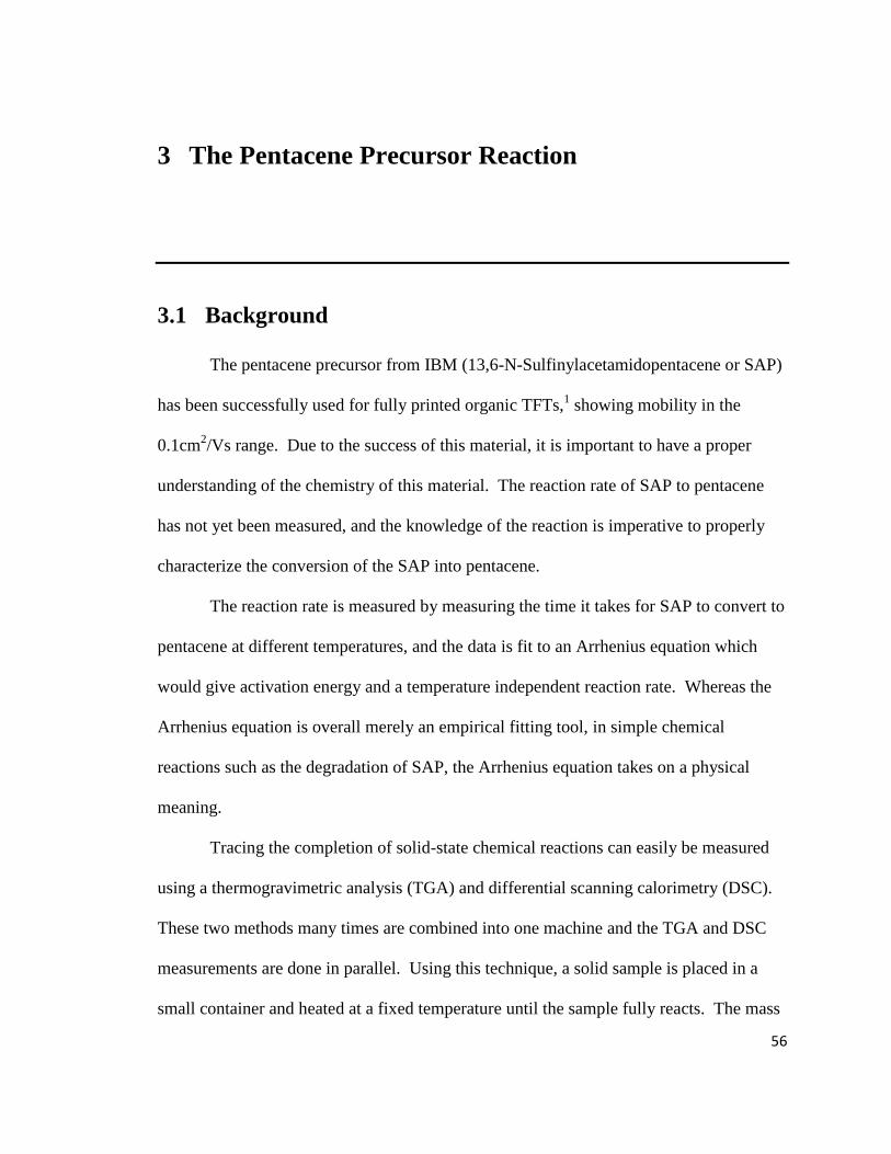
56
3 The Pentacene Precursor Reaction
3.1 Background
The pentacene precursor from IBM (13,6-N-Sulfinylacetamidopentacene or SAP)
has been successfully used for fully printed organic TFTs,1 showing mobility in the
0.1cm2/Vs range. Due to the success of this material, it is important to have a proper
understanding of the chemistry of this material. The reaction rate of SAP to pentacene
has not yet been measured, and the knowledge of the reaction is imperative to properly
characterize the conversion of the SAP into pentacene.
The reaction rate is measured by measuring the time it takes for SAP to convert to
pentacene at different temperatures, and the data is fit to an Arrhenius equation which
would give activation energy and a temperature independent reaction rate. Whereas the
Arrhenius equation is overall merely an empirical fitting tool, in simple chemical
reactions such as the degradation of SAP, the Arrhenius equation takes on a physical
meaning.
Tracing the completion of solid-state chemical reactions can easily be measured
using a thermogravimetric analysis (TGA) and differential scanning calorimetry (DSC).
These two methods many times are combined into one machine and the TGA and DSC
measurements are done in parallel. Using this technique, a solid sample is placed in a
small container and heated at a fixed temperature until the sample fully reacts. The mass

57
of the sample is traced as a function of time, and the heat flow in and out of the sample is
also traced as a function of time. Only one sample is needed for each temperature that is
to be measured. From sample to sample, the precise amount of material does not have to
be identical. Unfortunately, the machine cannot be brought to the reaction temperature
instantaneously. It takes a few minutes before the machine heats up from room
temperature to the reaction temperatures. This lag will give an inaccurate reading on the
reaction rate of SAP to pentacene at higher reaction temperatures. In Afzali’s original
paper, TGA was merely used to find the temperature where SAP decomposition begins
and also to find the reaction yield. It was found that SAP starts converting to pentacene
at 1200C, and the reaction yield is close to 100%.
In order to be able to properly trace the reaction completion of SAP conversion,
UV-vis spectroscopy was used to measure the reaction of the pentacene precursor
instead. The downside to this technique is that a large number of samples needs to be
prepared for this technique as compared to TGA-DSC. The preparation of each sample
needs to be identical otherwise the absorbance measurements would be meaningless.
With UV-vis, SAP is first deposited onto glass slides and then reacted on a hotplate. The
hotplate is set to the reaction temperature and samples are placed onto the preheated
hotplate. Since the slides are small and thin, the time lag to heat samples from room
temperature to the reaction temperature is short, so this method is more accurate than
TGA-DSC. In order to properly trace the reaction for each reaction temperature many
samples need to be prepared, with each sample reacted to various stages of reaction
completion. In order to trace a chemical reaction from beginning to end many samples
are needed so that the complete reaction can be captured.

58
3.2 Experimental Procedures
Solid-state UV-vis absorbance spectroscopy (UV-vis) was used to find the
reaction rate of pentacene precursor. UV-vis samples were prepared by spinning SAP
onto glass substrates. SAP was made by the method described in the Appendix. Glass
substrates were 22mm by 22mm glass microscope cover slips from Fisher Scientific.
Solutions were prepared by dissolving 12mg of SAP into 1mL of 99% anhydrous
chloroform stabilized with amylenes purchased from Aldrich. Solutions were deposited
onto the glass microscope cover slips at 0rpm (200l per cover slip). Once solutions
were deposited onto the glass substrates, the substrates were quickly ramped up to
4000rpm (within 2s) and spun at 4000rpm for 30s.
Each sample was then heated at a specific for a fixed amount of time. All
samples were heated in a dry nitrogen glovebox. Using the results of from Alfazi et al,2
it was determined that the decomposition temperature starts at ~1200C. The temperature
range used for sample heat should at least be 1200C. For each reaction temperature
multiple samples were used each being heated at different durations. For the lower
temperature points, more samples and longer total times were used in order to trace the
reaction rate more accurately. For the higher temperature points fewer samples were
used and shorter reaction times were used. The shortest sample heating times was 1s,
since placing samples on and off hotplates could not be accurately measured at times
shorter than 1s. Table 3.1 shows all the different heating conditions used.

59
Temperature Heating times
125 2.5m, 5m, 10m, 20m, 40m, 80m
130 15s, 30s, 45s, 1m, 2m, 4m, 8m, 16m, 32m, 64m, 128m
140 15s, 30s, 45s,1m, 2m, 4m, 8m, 16m, 32m
150 1m, 2m, 4, 8m, 16m, 32m
160 1s, 2s, 4s, 8s, 16s, 32s, 64s, 128s
170 1s, 2s, 4s, 8s, 16s, 32s, 64s, 128s
180 1s, 2s, 4s, 8s, 16s, 64s
190 1s, 2s, 4s, 8s
200 1s, 2, 4s, 8s
220 1s, 3s
Table 3-1: List of all the temperature time conditions used for UV-vis anaylsis
All samples were scanned with a UV-vis spectrophotometer at wavelengths
ranging from 800nm to 400nm. Pentacene should have a strong absorbance been below
400nm,2 however the glass slides used as substrates are not transparent below 400nm.
No peaks were found above 800nm, so those regions were truncated.
By using the prescribed method described earlier, the reaction rate of the SAP to
pentacene was extracted for each temperature and an Arrhenius relationship was fit to the
reaction rate.
3.3 Experimental Results
First a pentacene precursor baseline was measured. Between 400nm and 800nm
there were no distinct peaks that can be identified by UV-vis. A sample heated at 1400C
for 1hr had five distinct peaks can be easily identified in the 400nm to 800nm range, as
shown in figure 3.1. It was assumed that this sample was fully reacted. The most
pronounced peak is the peak is approximately at 667nm. There is clearly no peak at
667nm for an unreacted pentacene precursor film, so for reaction rate measurements,
reactions will be followed by watching the 667nm peak.

60
Figure 3-1: UV-vis absorption spectrum of pentacene precursor and pentacene thin-film
on glass. The precursor sample was an unreacted sample of pentacene precursor. The
Pentacene sample was a sample pentacene precursor reacted at 1400C for 1hr.
Since every sample was prepared using the solution concentration and deposited
with the same spin speed, every sample should have the same amount of starting material
and therefore it is valid to trace the peak height in order to determine the fraction of
reacted material.
The absorbance value of an unreacted sample at 667nm was found be
approximately 0.012. When the absorbance value at 667nm of a particular sample was
the same as the 667nm absorbance of another sample both heated at the same temperature
but at different times, it was assumed that the two films are fully reaction and 100% of
the SAP had turned to pentacene. It was determined that for all temperature points the
absorbance of a fully reacted film was approximately 0.15. Figure 3.2, shows how the
absorbance of the 667nm peak increases as the reaction proceeds at 1300C. The increase
0
0.02
0.04
0.06
0.08
0.1
0.12
0.14
0.16
0.18
0.2
400 450 500 550 600 650 700 750 800
Ab
sorb
ance
(A
U)
Wavelength (nm)
SAP
Pentacene from SAP
667nm peak

61
of absorbance at 667nm peak indicates that pentacene is being created and SAP is
disappearing.
Figure 3-2: The change of absorbance as the SAP reaction proceeds.
Using the absorbance data in figure 3.2, figure 3.3 was created using the using the
methods prescribed in chapter 2 in the section in UV-vis analysis. In Figure 3.3
aborbance values was converted to SAP concentration and show how SAP disappears
over time when reacted at 1300C.
0
0.02
0.04
0.06
0.08
0.1
0.12
0.14
0.16
0.18
0 20 40 60 80 100 120 140
Ab
sorb
ance
Reaction time (min)
Reaction Complete

62
Figure 3-3: Disappearance of SAP at 1300C traced by UV-vis.
The decomposition of SAP to pentacene can be described by the general reaction
A B + C, where A is the starting material SAP and B and C is the resulting product,
pentacene and the NSO adduct. This reaction is a first order reaction, where
disappearance of A can be described by:
Akdt
dA
Equation 3-1
Where k is the rection rate, and the solution of this differential equation is:
kteCtA 0)(
Equation 3-2
Where C0 is the starting concentration of the reactant A. Equation 3.2 can be rewritten
into linear form:
0.00%
10.00%
20.00%
30.00%
40.00%
50.00%
60.00%
70.00%
80.00%
90.00%
100.00%
0 20 40 60 80 100 120 140
Pe
rce
nt
of
SAP
left
Reaction time (min)

63
.)(ln constkttA
Equation 3-3
In Figure 3.4, figure 3.1 is replotted as a log(y) vs. linear(x) plot, and the slope of
line gives the reaction rate k. The data points more or less fall on a straight line showing
that using the first order degradation reaction is a valid assumption.
Figure 3-4: log-linear plot of SAP disappearance at 1300C in order to extract reaction
rate.
The same figures were reproduced for every reaction temperature. As expected,
reactions occur much faster at higher temperature than lower temperatures. Due to the
high reaction rates at higher temperatures, films are fully converted to pentacene within a
few seconds at 1900C. The reaction rate extractions for these data points may not be
accurate, because of sample heating issues. Figure 3.5 shows the same graphs plot for the
SAP decomposition reaction at 1600C. Notice the compress x-axis showing that the
y = -0.0424x + 0.0054
-1.6
-1.4
-1.2
-1
-0.8
-0.6
-0.4
-0.2
0
0 5 10 15 20 25 30 35
ln(%
of
SAP
re
mai
nin
g)
Reaction time (min)

64
reaction procedures faster at higher temperatures. Here the decaying exponential still
works quite well to describe the disappearance of SAP.
Figure 3-5: (top) Linear-linear plot of SAP disappearance at 1600C. (bottom) Log-
linear version of SAP disappearance at 1600C.
It roughly takes 2-3 seconds for the glass coverslip to go from room temperature
to 90% of hotplate temperature once the sample is placed on the hotplate. At low
0.00%
10.00%
20.00%
30.00%
40.00%
50.00%
60.00%
70.00%
80.00%
90.00%
100.00%
0 1 2 3 4 5
Pe
rce
nt
of
SAP
left
Reaction time (min)
y = -2.8167x + 0.1576
-3.5
-3
-2.5
-2
-1.5
-1
-0.5
0
0.5
0 0.2 0.4 0.6 0.8 1 1.2
ln(%
of
SAP
re
mai
nin
g)
Reaction time (min)

65
temperatures where the reaction requires up to 1 hr for reactions to fully occur this 2-3
transient is not a problem. At high temperatures where reactions start before the sample
reaches the final temperature, we will get an underestimation of the reaction rate. Figure
3.6 shows the disappearance of SAP when reacted at 1900C. This figure clearly
demonstrates the pitfalls of the experimental setup. The first three points shows little
disappearance of SAP as the glass coverslip slowly heats up. Between the third and
fourth data point, the SAP concentration suddenly drops to 0, so the shape of the
decaying exponential is not captured. For these two reasons, the reaction rate extractions
at high temperature is clearly inaccurate.
Figure 3-6: linear-linear plot of SAP disappearance at 1900C
Table 3.2 shows the extracted reaction rates for each reaction temperature. This
data can be plotted according to the Arrhenius relationship:
RTEaekk/
0
Equation 3-4
0
0.2
0.4
0.6
0.8
1
1.2
0 0.02 0.04 0.06 0.08 0.1 0.12 0.14
Pe
rce
nt
of
SAP
left
Reaction time (min)
Reaction lag due to sample heating
up The concentration of SAP drops
to 0 too quickly and the shape
of the exponential decay is not
properly captured by the
sample
66
Here, k is the reaction rate of reaction, k0 is the reaction rate constant, Ea is the activation
energy and R is the gas constant. Figure 3.7 shows the reaction rates plotted in a log-
linear fashion to extract the activation energy. The activation energy was estimated to be
123.2kJ/mol.
Temperature Reaction rate (min-1
)
125 0.037533
130 0.042407
140 0.063045
150 0.597243
160 2.773099
170 1.785336
180 11.79519
190 6.975172
200 28.81501
220 13.69029
Table 3-2: Reaction rates for different temperatures
Figure 3-7: Reaction rates were fitted to an Arrhenius relationship in order to estimate
activation energy.
0.01
0.1
1
10
100
0.0015 0.0017 0.0019 0.0021 0.0023 0.0025 0.0027
Re
acti
on
rat
e (
min
-1)
Temperature (1/K)

67
3.4 Discussion
Using UV-vis the product of SAP decomposition has been confirmed to be
pentacene, since the UV-vis spectrum matches properly to the reported UV-vis spectrum
of evaporated pentacene as well as pentacene from SAP as seen in literature. Further
more the reaction rate of SAP degradation has been extacted using UV-vis absorbance.
The degradation of SAP was modeled using a 1st order reaction. The data fit well with
the 1st order reaction as predicted based on the chemical equation of SAP decomposition.
Finally the reaction rates were fit to the Arrhenius equation for the extraction of the
activation energy.
A chemical reaction in the form of a first order equation is only required to take
the form of a decaying exponential when the reaction takes place in gas phase. In liquid
phase the decaying exponential also occurs when the reactants are in low concentrations.
For a solid-state reaction which is the case of a pentacene thin film from SAP, the
decaying exponential does not necessarily take place. In solid state reactions, energy is
necessary not only to cause a transformation either in phase or to cause a chemical
reaction to take place, but energy also needs to be placed into nucleation and crystal
growth, therefore a simple exponential decay may not necessarily describe a solid-state
reaction.
Typically in a solid-state phase transformation or chemical reaction, the
transformation can be described with a sigmoidal curve which is described using the
Avarmi equation.

68
1F(t) exp Ktn
Equation 3-5: Avrami equation, where F(t) is the fraction of starting material reacted, n
and K determine film growth mechanisms.
When the data point from 1250C to 160
0C is fit to the Avarmi equation, n = 1. When n =
1, the Avrami equation is precisely an exponential decay. Only these five temperature
were used in the extraction, because these five points have the least measurement errors.
This extraction indicates that the use of using the exponential decay is valid.
The fact the data fits nicely using a decaying exponential and the follows the
Arrhenius equation nicely is probably due to the simplicity of the reaction. The reactant
only needs “fall apart,” and does not need to collide with another reactant, therefore even
though the reactant is in the solid state the mechanism for the chemical reaction to take
place is extremely simple. Most likely the most energetically costly step in the formation
of pentacene is the decomposition of SAP. The appearance of pentacene is apparently
not hindered by nucleation or crystal growth, this may be another reason for a simple
exponential decomposition.
After calculating the reaction rate the formation of pentacene from SAP needs to
be looked at in more detail. How exactly does pentacene nucleate to form pentacene
films? This is the subject of the next chapter. Knowing the reaction rate is important
when looking at the formation of pentacene films, so that it can be determined the amount
of pentacene and SAP present at any given time.

69
3.5 Conclusion
Using UV-vis the retro Diels-Alder reaction rates was measured. Measuring the
reaction rate of the pentacene precursor allows for proper control of reaction times. It has
been suggested that the greatest energetic step in pentacene formation is the SAP to
pentacene retro Diels-Alder reaction and not the formation of pentacene crystals and
nuclei. More experiments still need to be done in order to gain more insight on pentacene
formation through SAP.

70
3.6 References
1. Molesa, S. et al. A high-performance all-inkjetted organic transistor technology.
Electron Devices Meeting, 2004. IEDM Technical Digest. IEEE International 1072-
1074(2004).doi:10.1109/IEDM.2004.1419384
2. Afzali, A., Dimitrakopoulos, C. & Breen, T. High-performance, solution-processed
organic thin film transistors from a novel pentacene precursor. JOURNAL OF THE
AMERICAN CHEMICAL SOCIETY 124, 8812-8813(2002).

71
4 The Pentacene Thin-film growth on SiO2 from
Pentacene precursor
4.1 Background
Pentacene TFTs have been made and tested quite extensively. Even though one
of the goals of pentacene is for flexible electronics, the most typical substrate pentacene
is deposited on is still amorphous SiO2 (a-SiO2). The backgated TFT is the easiest test
bed for testing organic materials. Thermal evaporation is the most common and the
easiest way to deposit pentacene onto silicon dioxide. One of the major points of study
these past years in organic electronics is pentacene thin-film growth on SiO2. At this
point the thin-film growth mechanism of pentacene on a-SiO2 is very well known. This
knowledge has aided in understanding the electrical properties of pentacene TFTs on
SiO2. The focus of this chapter is on the thin film growth of pentacene through thermal
degradation of SAP on a-SiO2. A simple review of the growth of pentacene through
evaporation serves as a model and point of comparison for pentacene growth through
solution methods.
4.2 Growth of Pentacene on SiO2 through Evaporation
It is known that bulk pentacene packs in the herring-bone structure creating a
triclinic unit cell.1 Pentacene films grown on a-SiO2 are textured perpendicular to the

72
substrate and exist in three polymorphs.2 The herring-bone packing is present in each of
these polymorphs; however, lattice constants and angles between the pentacene
molecules and pentacene to substrate change with the energetic interaction between
pentacene and the oxide substrate.
The different polymorphs of thin-film pentacene are thickness dependent. The
first monolayer of pentacene deposited stands nearly perpendicular to the oxide substrate,
taking an orthorhombic crystal structure. This is the monolayer phase of pentacene.2,3
After a second layer of pentacene is formed on top of the first monolayer, the first
monolayer relaxes and now the two monolayer film both become triclinic. The lattice
constants and angles, however, are not same as bulk triclinic pentacene. This polymorph
of pentacene is referred to as the thin-film phase of pentacene.2-4
Each monolayer of
pentacene is approximately 16Å. The thin-film phase of pentacene persists for
approximately 10 monolayers of pentacene or a total of approximately 16nm. Both of the
monolayer and thin-film phase of pentacene are textured perpendicularly to the substrate.
After approximately 20nm of pentacene is deposited, the third polymorph of
pentacene appears. This phase of penatcene is called the bulk-like phase, because it is the
most the most relaxed phased and most similar to bulk pentacene. The bulk-like phase of
pentacene forms islands on top of the ~10 monolayer of thin-film pentacene. This is
classic Stranski-Krastonov film growth. The S-K islands are textured perpendicular to
the thin-film phase of pentacene. The textured island growth of bulk-like pentacene
continues until a total film thickness of approximately 40nm.2-4
After growing an approximately 60nm film of pentacene, texturing of the bulk-
like phase stops, and untextured bulk-like pentacene crystals start growing on top of the

73
well textured film.3-6
This thickness dependent film growth of pentacene is summarized
in figure 4.1.
Figure 4-1: Summary of thickness dependent thin film growth of pentacene on oxide
The bulk triclinic phase of pentacene is the thermodynamically stable polymorph
of pentacene. The orthorhombic monolayer of pentacene is the least stable phase of
pentacene. The first monolayer takes the orthorhombic configuration because it matches
the substrate energetically. Pentacene thin film growth is a good example of the Ostwald
principle of thin-film growth. The Ostwald principle states that in thin-film growth the
unstable phase condenses first before a more stable phase forms.
For high performance pentacene TFTs it is important to have large highly textured
pentacene films with large crystallite sizes.7 Mobility has also been shown to be higher
in the thin-film polymorph versus the bulk-like polymorph.8 Therefore, thermal
evaporation of pentacene for pentacene-TFTs on a-SiO2 is always evaporated slowly, at
~10Å/min, in order to encourage proper crystal ordering. Invariably slow evaporation is

74
coupled with substrate heating at ~700C to aid in pentacene molecular mobility and allow
for grain growth.9,10
Currently, little is known about the growth of pentacene thin films using SAP.
Solution processed pentacene TFT been made using this precursor is usually deposited
onto the substrate drop-by-drop through inkjet printing or spinning. The deposited film is
then heated on a hotplate at a fixed temperature anywhere from 1200C to 200
0C for an
arbitrary time. Little is known about the reaction rates of this precursor degradation.
Neither is the film formation mechanism of this solid-state reaction known.
Currently very few studies have been performed to look at pentacene film from
SAP. One study looked at the initial stages of film development using a Langmuir-
Bloggett films of SAP two different substrates. It was found that a Volmer-Weber island
growth was favored on the substrate with a lower surface free-energy, and a Stranksi-
Krastonov growth was favored on the substrate with higher surface free-energy.11
An X-
ray study has been performed on the crystal structure of pentacene from SAP films,12
however film development was not explored and a detailed study of film was not
performed. Pentacene-TFTs from have been found to have the highest mobility the
pentacene precursor is heated at 1600C for approximately 5 minutes. The reason for the
high mobility was not known.13,14
From the previous chapters the reaction rate has finally been measured using UV-
vis. This information is useful to determine the minimum heating time to fully transform
the precursor to pentacene. This chapter focuses to understand the growth of pentacene
thin films on a-SiO2 using SAP. The formation of pentacene thin films is traced using

75
SEM. AFM is used to look at the topology of these films and finally GIXD is used to
identify the different pentacene phases.
Even though a fully solution processed organics TFT would never use a-SiO2,
however, a-SiO2 is still the most commonly used gate dielectric material for pentacene
TFT testing. Since, the growth of pentacene thin films through thermal evaporation onto
a-SiO2 is well understood and serves as a good reference point for comparison for
pentacene thin-films through pentacene precursor.
4.3 Experimental Procedures
4.3.1 Preparing Pentacene precursor on Oxide
SAP was spun on standard undoped oxidized wafers. SAP solutions were
prepared by dissolving the precursor into anhydrous chloroform stabilized with amylene
from Aldrich (12mg/mL). SAP was prepared according to the methods in Appendix A,.
Solutions were vortexed in a vortexer until the solute was fully dissolved. The solution
has a clear to a light orange color. 1mL of solution was dispensed onto each wafer.
Solutions were dispensed at 0 rpm. After dispensing the solution, the wafer was ramped
up to 4000 rpm within 2s and spun at 4000 rpm for 30s. Finally, the wafer is diced into
1cm×1cm pieces.
4.3.2 Heating of conditions of samples to trace pentacene growth
Each sample was heated on a hotplate in a glovebox under dry nitrogen ambient.
Table 4.1 shows all the time-temperature conditions which samples were heated at. Each
sample was placed on a preheated hotplate and heated for the prescribed time. Once the

76
prescribed time is reached, samples are removed from the hotplate and placed ontop of a
metal plate for cooling.
Temperature Heating time
125 30s, 1m, 5m, 10m, 15m, 20m, 30m, 40m, 90m, 180m
130 15s, 30s, 45s, 1m, 2m 4m, 8m, 16m, 32m, 64m, 128m
140 15s, 30s, 45s, 1m, 2m 4m, 8m, 16m, 32m
150 15s, 30s, 45s, 1.5m, 4m, 8m, 16m, 32m
160 1s, 2s, 8s, 16s, 32s, 64s, 128s, 4m
170 1s, 2s, 4s, 8s, 16s, 32s, 64s, 2m
180 1s, 2s, 4s, 8s, 16s, 32s, 64s
190 1s, 2s, 4s, 8s, 16s, 32s
200 1s, 2s, 4s, 8s, 16s, 32s
220 1s, 2s, 4s, 8s, 16s, 32s
240 1s, 2s, 4s, 8s, 16s
260 1s, 2s, 4s, 8s, 16s
Table 4-1: Sample conditions for SEM
4.3.3 SEM imaging
SEM images were imaged at 5kV. Images process through the open source
software The GIMP. Images were checked for number of pentacene nucleation sites.
Crystal growth was monitored and measured by finding the characteristic length of
pentacene islands. The characteristic length reported is the average value of multiple
islands. The pentacene islands were measured by the scheme in figure 4.2. Finally,
dewetting of films from the substrate was noted.

77
Figure 4-2: Calculation of characteristic length. 21 rrLc
4.3.4 AFM imaging
On select samples, a surface topological image was taken using an AFM. All
AFM images were taken through tapping mode surface contour measurements. Images
were processed through the open source software Gwiddyon.
4.3.5 GIXD
GIXD was performed on another set of samples prepared the same way as noted
above. Each sample was made into a 2cm × 2cm pieces. The heating conditions were
according to table 4.2. Times were chosen to ensure that reactions have gone to
completion.
Temperature Heating times
125 180m
140 16m
160 2m
180 64s
Table 4-2: Sample conditions for GIXD

78
4.4 Results
4.4.1 Qualitative SEM results
There appear to be two temperature regimes of pentacene film growth, a low
temperature regime (1200C to 140
0C), and a high temperature regime (160
0C to 200
0C).
At intermediate temperatures, there appears to be a mixed film growth resembling both
high and low temperature film growth. At temperatures above 2000C, there is rapid
pentacene film formation and a large amount of film dewetting from the substrate.
4.4.1.1 Qualitative description of low-temperature film growth
For low temperature film development at 1250C, white pentacene crystals islands
are clearly visible after heating the precursor for 30s (figure 4.3). At this point, most of
the film is still unreacted pentacene precursor, this seen as the dark parts around the white
islands. Each island indicates a nucleation sites. The islands all have approximately the
same size. With continued heating, the islands continue to grow and are clearly
polycrystalline (figure 4.4). The polycrystalline islands clearly look like a group of
triclinic crystals merged together. This is expected because pentacene usually takes a
triclinic crystal structure.6 After more time, the polycrystalline islands stop growing in
size, even though the film has not fully reacted. Around the poly crystalline island, there
is clear growth of a pentacene thin film.

79
Figure 4-3: Nucleation of pentacene (1250C, 30s)
Figure 4-4: The initial nucleation sites have become polycrystalline islands. The light
gray around the islands is a thin film of pentacene. The smaller islands are SK islands on
top of the thin film. (1250C,30min)

80
Figure 4-5: fully reacted pentacene film (1250C, 3hr)
As the pentacene thin film grows and covers the regions around the
polycrystalline islands with pentacene, small pentacene islands grow on top of the
pentacene thin film. Again these islands have the characteristics of a triclinic crystal
(figure 4.4). These small islands are seen starting after 10 minutes of reaction time.
After three hours of heating, the pentacene precursor should be fully reacted; all
three aforementioned features are clearly visible, the polycrystalline islands, pentacene
thin-film around the islands, and smaller islands on top of the thin film (figure 4.5).
Small pentacene islands growing on top of a pentacene film matches the description of
typical Stranski-Krastonov film growth. This is again expected, because pentacene
grows in S-K mode when evaporated on top of oxide.2,15
4.4.1.2 Qualitative description of high temperature film growth
For films processed at 1600C to 200
0C, the formation of a pentacene thin-film
looks completely different than the formation of a pentacene thin-film below 1300C.

81
There does not appear to be any of the low temperature island nucleation sites. Instead
there are large black spots which appear during the early parts of the precursor reaction
(figure 4.6). The spots are blurry and difficult to focus with SEM. These spots are
located at the interface between pentacene precursor and the oxide and not in the
precursor matrix.
Figure 4-6: High temperature nucleation. (1500C, 15s)
As heating time is increased, the spots become larger, but the size quickly
becomes fixed. After more heating, the spots become more visible and easier to focus,
crystallines edges characteristic of a triclinic crystal lattice once again start appearing
(figure 4.7). Instead of large islands, these spots end up looking like flat plateaus. The
boundaries of the islands are distinct and only a little bit larger than the original black
spots which appeared early in film formation.

82
Figure 4-7: Crystal grown on the high temperature nucleation. (1500C, 45s)
Once the reaction is complete, around the plateaus there is dewetting (figure 4.8),
which is highly visible for films processed above 1800C. For films processed at a lower
temperature there is less dewetting, and a thin film of pentacene is formed in between the
plateaus instead. On top of the thin film, smaller pentacene islands also grow, once again
showing typical Stranski-Krastonov film growth.

83
Figure 4-8: Dewetting on fully develop films. (1800C,1min)
4.4.1.3 Qualitative description of film grow at intermediate temperatures
At intermediate temperatures (1400C - 160
0C), a mixed film growth occurs. After
15 seconds of heating at 1400C, both the low temperature islands appear as well as high
temperature black nucleation spots (figure 4.9). As the reaction proceeds the size of the
low temperature islands grow slightly. It appears that material preferentially goes to the
high-temperature black nucleation spots instead of the low temperature nucleation
sites(figure 4.10). After 4 minute of heating at 1400C crystalline edges appear on the
black nucleation spots (figure 4.10).

84
Figure 4-9: Mixed nuclation (1400C, 1min)
After 4 minutes of heating, a thin film of pentacene has formed around the low
temperature islands. Once again small islands developed on top of the thin film. The
high temperature spots develop as it would at high temperatures, however, are not as
“complete” as at high temperatures. Instead of forming a flat plateau, a “crescent” shape
is formed instead (figure 4.10).

85
Figure 4-10: Crystal grown on mixed nucleation (1400C, 4min).
Figure 4-11: Fully reacted pentacene film (1400C, 32min).
At 1500C, the low temperature islands grow significantly less than the black high
temperature nucleation. The final fate of the low temperature islands is difficult to
determine because there were very few low temperature islands formed. From the

86
conception of the low temperature islands to the time the film fully develops, little
growth occurs with the low temperature islands, so the islands are difficult to identify
after the film is fully developed. The black high temperature islands once again becomes
crescents once films are fully developed (figure 4.12). As usual, small S-K islands
growing on top of the thin film in between the crescents. The small S-K islands are
smaller and become more numerous at 1500C in size versus 140
0C.
Figure 4-12 Fully reacted pentacene film (1500C, 16 min). Note that the SK-islands are
more numerous than compared to 1400C.
4.4.2 Quantitative SEM results
For each SEM image, the size and density of both low temperature islands and
high temperature black spots were counted and the characteristic lengths were measured.

87
4.4.2.1 Nucleation sites
Both the high temperature and low temperature nucleation density remain
relatively constant throughout film formation. In other words from beginning to end of
film formation there does not seem to be an increase or decrease of nucleation sites for
both types of nuclei (figure 4.13 and 4.14). However, as processing temperature
increases the number of low temperature nuclei decrease while the number of high
temperature islands increase. Figure 4.14, summarizes the interplay between low
temperature nuclei and high temperature nuclei. Low temperature islands were observed
in films process from 1250C to 150
0C. High temperature nucleation spots were observed
starting at 1400C. At temperatures above 160
0C, low temperature islands are no longer
observed. The formation of low temperature islands becomes less favorable as
temperature increases and the high temperature nuclei become more favorable.
Figure 4-13: Density of nucleation sites stays constant throughout film development at
1250C. This is true for all films at low temperatures.
0
0.01
0.02
0.03
0.04
0.05
0.06
0 10 20 30 40 50
De
nsi
ty o
f n
ucl
eat
ion
sit
es
(μm
-2)
Reaction time (minutes)

88
Figure 4-14: Density of nucleation sites stays constant throughout film development at
1600C. This is true for all films at high temperatures.
Figure 4-15: Temperature interaction between high and low temperature nucleation
sites.
0
0.02
0.04
0.06
0.08
0.1
0.12
0 1 2 3 4 5
De
nsi
ty o
f n
ucl
eat
ion
sit
e (
µm
-2)
Reaction time (minutes)
0
0.02
0.04
0.06
0.08
0.1
0.12
0.14
0.16
0.18
0.2
0
0.005
0.01
0.015
0.02
0.025
0.03
0.035
0.04
0.045
0.05
120 140 160 180 200 De
nsi
ty o
f h
igh
te
mp
era
ture
nu
cle
atio
n
site
(μ
m-2
)
De
nsi
ty o
f lo
w t
em
pe
ratu
re n
ucl
eat
ion
si
tes
(µm
-2)
Reaction Temperature (0C)

89
Not only does the density of low temperature islands decrease with increased
temperature, but the final characteristic length of the low temperature islands also
decreases with increased temperature. The high temperature plateaus increase in density
with increased reaction temperature and decrease in characteristic length with increased
temperature (figure 4.16).
Figure 4-16: The effect of temperature on the final size of both high and low temperature
islands.
4.4.2.2 Crystal Growth
Absolute time cannot be used to compare samples reacted on temperature,
because from one temperature to another, reaction rates differ, so the amount of
pentacene available for film formation is different for each sample. When comparing
between samples processed at different reaction temperatures, instead of using absolute
time, time was normalized to the reaction rate (real time×reaction rate). This way,
samples with different reaction temperatures can be compared to each other. Normalized
0
0.5
1
1.5
2
2.5
3
3.5
4
4.5
0
0.5
1
1.5
2
2.5
120 140 160 180 200
Ch
arac
teri
stic
len
gth
of
hig
h
tem
pe
ratu
re is
lan
ds
(μm
)
Ch
arac
teri
stic
Le
ngt
h o
f lo
w
tem
pe
ratu
re is
lan
ds
(µm
)
Reaction Temperature (0C)

90
time () indicates the percentage of starting material that reacted. For example, at of
0.69 shows that 50% of the starting material has finished reacting.
Figure 4.17, indicates that lateral low temperature islands growth ceases at a later
than at higher temperatures. In terms of reaction completion, this means that as the
reaction temperature is increased the supply of pentacene to low temperature islands
stops at an earlier stage of reaction, but instead pentacene is supplied to the high
temperature nuclei, therefore low temperature island growth is stunted, and high
temperature features dominate.
Figure 4.17 also shows the when high temperature plateaus stops lateral growth.
The plot shows some fluctuations, however is probably actually constant. Unfortunately,
the samples were not created such that each reaction temperature has the same exact
number of samples and with each the corresponding for each temperature. Hence the
fluctuation in the data is from lack of data points.
In the intermediate temperature range, where high temperature and low
temperature nuclei form, the where lateral growth stopped is approximately the same
for both high temperature plateaus and low temperature islands.

91
Figure 4-17: The effect of temperature on the time of lateral island growth stops.
4.4.3 AFM results
AFM was used to find the topology of SAP films at various phases of film
development. By looking for defects in unreacted films of pentacene precursor, it was
found that the spun-on pentacene precursor films on oxide were approximately 25-40nm
in thickness.
4.4.3.1 AFM images for films processed at 1250C
AFM images for film processed at 1250C for only 5 minutes were taken (figure
4.18). The image shows a valley at the base of low temperature islands showing the
consumption of pentacene precursor around islands. The cross-section of an island,
shows that the valley is approximately 40 nm deep, which is the thickness of the
precursor film.
0
0.1
0.2
0.3
0.4
0.5
0.6
0.7
0.8
0.9
1
120 130 140 150 160 170 180 190
No
rmal
ize
d r
eac
tio
n t
ime
Reaction Temperature (0C)
Low temperature islands
High temperature islands

92
Figure 4-18: AFM of low temperature islands. Pentacene precursor consumption
around the islands is quite apparent. (1250C, 5min)
4.4.3.2 AFM images for films processed at 1600C
An AFM images taken of SAP films processed at 1600C for 4 seconds showed the
the early stages of pentacene film development (figure 4.19). This was to specifically
image the high temperature nuclei. The thickness of these spots were measured to be
anywhere from 1.5nm to 3nm. This corresponds to 1 to 2 monolayers of pentacene
respectively. This is strong evidence that at high temperatures nucleation of pentacene
forms monolayers of pentacene on top of the oxide, instead of forming islands as seen at

93
low temperatures. It should be noted that because these monolayers form at the interface
of the oxide to the pentacene precursor. AFM measurements are not actually in contact
with the pentacene itself, but with the unreacted precursor instead. The formation of the
pentacene monolayers create a bump in the top surface of the uncreated precursor on top
of the monolayer, therefore the actual thickness of these pentacene monolayers are
merely an estimate.
Figure 4-19: AFM of a high temperature nucleus. The thickness of nucleus corresponds
to approximately 1 monolayer of pentacene. (1600C, 4s)

94
4.4.3.3 AFM images of fully developed films at different temperatures
AFM images of fully reacted films processed at 1250C and one processed at
1800C (figure 4.20) were used to find the rms roughness of films. The rms roughness of
both films was found (table 4.3). The film at high temperatures was much smoother than
low temperature films. This makes sense from what was has already been deduced from
SEM and AFM. Pentacene formation at low temperatures creates islands, while
pentacene formations at high temperatures is formed layer by layer. Based on the
roughness values at 1800C, this roughness is very much a result of dewetting of the
pentacene from the substrate. Without dewetting, high temperature pentacene films
would be quite smooth. Pentacene formed at low temperatures initially start with island
formation, so the final film consists of many large islands, hence making the final film
extremely rough due to many valleys and peaks.

95
Figure 4-20: AFM a fully reacted film showing dewetting. (1800C, 1min)
Temperature 125 180
RMS roughness (nm) 127 25.5
Table 4-3: Roughness of films
4.4.4 GIXD Results
Texturing was the most prominent at 1600C (figure 4.23), where the mixed
reflections are clearly seen, and the arcing is the least. As temperature is decreased from
1600C, the spots blur and large arcs are seen instead. Moving from 160
0C to a higher
temperature, the arcing is also larger compared to arcing at 1600C. This indicates that
surface texturing is maximized at 1600C. However, comparing the degree of texturing at
1800C (figure 4.24) vs. 125
0C (figure 4.21), it is still much more textured at 180
0C than at

96
1250C. Low temperature films are more disordered versus higher temperature films.
This shows that the low temperature crystals grow independent of the substrate and the
crystal orientation is random. The high temperature islands are textured perpendicular to
the substrate showing that the substrate plays a role in high temperature crystals.Only
bulk-like pentacene was found on the low temperature samples (figure 4.21). Both thin-
film and bulk-like phase was found on pentacene films processed at higher temperatures.
The thin-film phase is seen through the doubling of peaks in the 300 planes (figure 4.22-
24). The double peaks show that there are two 300 planes in existence, showing two
morphotypes coexisting. The peak doubling is only seen in higher temperatures and not
lower temperatures.
Figure 4-21: 2D GIXD plot for a film processed at 1250C

97
Figure 4-22: 2D GIXD plot for a film processed at 1400C
Figure 4-23: 2D GIXD plot for a film processed at 1600C

98
Figure 4-24: 2D GIXD plot for a film processed at 1800C
The 100 peak was measured in higher resolution using the 7-2 beam line. By
measuring the 100 peaks width the comparison of crystallite size can be calculated. For
simplicity the crystals were assumed to take on a cubic structure, hence the extracted
crystal size is merely an estimated (figure 4.25). The diffraction patterns suggest that at
low temperatures the crystallite sizes are largest since the peaks the narrowest. As
temperature increases, the crystallite size decrease since the peaks are more spread out.
This shows that at low temperatures, slow crystal growth promotes the increase of
crystallite size, whereas at high temperatures fast growth of crystal promotes nucleation
of pentacene crystals but decreases the crystallite size. Unfortunately, there was not
enough time to use the high resolution diffraction to obtain the crystallite size of at
1250C. However, from the 2-D low resolution plots, it can be seen that the 100 peak at

99
1250C is much narrower than the other processing temperature, indicating a larger
crystallite size.
Figure 4-25: Crystallize size due to processing temperature
4.5 Discussion
From the SEM images, the existence of two modes of pentacene nucleation can be
seen; one at low temperatures (1200C-130
0C) and one at high temperatures (160
0C+).
Both modes of nucleation showed a constant density with respect to reaction time.
However, there is a change in nucleation density with respect to temperature. Previously,
it was suggested that this indicates a heterogeneous mode of nucleation, where defects on
the substrate helps catalyze nucleation of pentacene. However, the increase of nucleation
density from temperature may indicate that the nucleation density affected by the
precursor more than the substrate, and that the formation of nuclei is homogenous and not
heterogeneous. The formation of pentacene nuclei in the precursor can be thought of as
inclusion forming in a matrix, and the temperature changes the density of inclusions
0
20
40
60
80
100
120
120 130 140 150 160 170 180 190
Cry
stal
lite
siz
e (
angs
tro
ms)
Processing Temperature (0C)

100
which are formed, homogenously. The thought of inclusions in a matrix parts from the
paradigm of thin film formation where the substrate plays an important role in
crystallization. The appearance of two types of nuclei, where one seems to be substrate
dependent shows that thin-film ideas are definitely at play. Therefore, there is both thin-
film mechanism as well as bulk solid crystallization mechanisms at work.
At low temperatures, the reaction is extremely slow. Therefore the supply of the
pentacene for film formation is very slow. Due to the slow reaction pentacene molecules
have time to arrange themselves slowly. With the help of the matrix to stabilize
pentacene crystals along with the slow crystal growth the thermodynamic product (bulk-
like phase) is formed at low temperatures. This explains why no texturing is seen at low
temperatures. Since the bulk-like phase is unstable on top of oxide, the bulk-like phase
has no regards for the substrate and grows in arbitrary orientations. The exclusive growth
of the bulk-like phase is not seen in thermal evaporation. This results because during
evaporation, the supply of pentacene to the substrate is much faster than the supply of
pentacene to the substrate from SAP reaction at low temperatures. Also with thermal
evaporation, there is not a stabilizing matrix to help the bulk-like phase to grow.
The low temperature nuclei eventually form large polycrystalline islands. This
further indicates the unfavorable interactions between the pentacene and oxide. An
upward growth in lieu of a lateral growth is an attempt to minimize substrate interactions
with pentacene. The vertical growth of islands is stopped as SAP around islands is
consumed. The size of pentacene islands is limited by SAP film thickness.
Due to the low molecular mobility of pentacene at the low temperatures, not all
pentacene molecules are able to travel to islands and aid in islands growth, instead a thin
101
film of pentacene also grows between islands. Once the thin film of pentacene grows,
small pentacene islands nucleate on top of the thin film. Due to the slow reaction rate of
the pentacene at low temperatures, crystallites are allowed to grow much larger. For the
same reasons, these islands are larger at lower temperatures vs. higher temperatures.
At high temperature the appearance of pentacene is quite rapid, creating a
different type of pentacene nuclei and the less stable thin-film phase forms. Here the
growth looks more like pentacene growth through evaporation layer-by-layer. Pentacene
nucleation starts as thin film phase monolayers of pentacene instead of islands. The
formation of the thin-film phase is caused by a substrate interaction. The fact that the
thin-film phase forms at higher temperature shows that as reaction temperature increases,
the energetic effect of the substrate also increases, and the matrix plays a smaller
energetic role in nucleus formation. Physically what may be happening is that an
increased in processing temperature increases the reaction rate of pentacene conversion.
This translates to an increased rate of pentacene appearance. Kinetic products are usually
favored in lieu of the thermodynamic product during rapid reactions, so the thin-film
phase is favored.
Since the substrate plays a role in the film formation, texturing perpendicular to
the substrate is observed; similar to what is seen in evaporated pentacene. With the help
the SAP matrix, after the formation of a few layers of the thin-film phase the bulk-like
phase starts to grow. Due to the help of the matrix, pentacene is able to relax much faster
than on evaporated film. This explains why so little thin-film phase of pentacene is
formed. Due to the negative interactions between the pentacene and oxide, pentacene
preferentially grows upward instead of laterally and causes dewetting on the substrate.

102
When the temperature is raised even higher, the reaction rate increases and
nucleation sites became extremely numerous. Crystal growth also become even more
rapid. Both these factors create small pentacene crystals. Furthermore texturing is
slowly lost from rapid nucleation and crystal growth.
At intermediate temperatures, both types the high temperature and low
temperature nuclei are formed. The ratio of high:low temperature nuclei depends on the
reaction temperature. At higher temperatures, the high temperatures nuclei dominate and
become more numerous. When the high temperature nuclei coexist with the low
temperature nuclei, crystal growth from the high temperature nuclei is preferential over
the low temperature nuclei. Since the high temperature nuclei are large flat spots, these
nuclei formed a stable surface for pentacene crystals to grow on top of. The growth of
low temperature islands require pentacene molecule to grow laterally as well as
vertically, lateral growth is always unfavorable because it requires an unfavorable
interaction with the substrate.
Also, at intermediate temperatures pentacene does not dewetting from the
substrate, instead a thin film of pentacene grows between both the high temperature
plateaus and low temperature islands. SK islands form on top of pentacene thin film. At
high temperatures, the SK islands are smaller and more numerous due to the rapid supply
of pentacene. At lower temperatures there are larger but fewer SK islands, because of the
slow supply of pentacene. Figure 4.26 summarizes the effects of time and temperature on
growing pentacene films on oxide.

103
Figure 4-26: Time-temperature dependency on pentacene film growth from SAP.
The trends previously observed in TFT measurements can now be explained from
the knowledge gleamed from pentacene film formation. The highest mobility is reported
at intermediate temperatures.14
The peak mobility falls between 1500C and 160
0C.
GIXD data show that there is the highest amount texturing in that particular temperature
range. The thin-film phase of pentacene is also present in that temperature range. The
high texturing and existence of the thin-film phase helps to give high mobility. Texturing
is extremely low at 1250C, and only the bulk-phase of pentacene is observed and gives
low mobility. At 1800C, the mobility should also be low compared to intermediate
temperatures.
Even though at this temperature there is the thin-film phase and some texturing,
however, the texturing at this temperature is lower than at intermediate temperatures. At

104
high temperature the rapid growth of films causes disorder, so texturing is lost. The rapid
growth of crystals also decreases the crystal size. Finally, dewetting is pronounced at
1800C. Decreased texturing, small crystal size and dewetting all contribute to the low
mobility at high temperatures.
Regarding on/off ratios, at high temperatures the on/off ratio is the highest. Films
processed at high temperatures have the fewest defects as well as miscellaneous
byproducts from the precursor degradation giving the highest on/off ratio. The amount of
byproducts and defects at lower temperatures keeps the on/off ratio relatively low.
As a final note, it is interesting that the thin-film phase persists in the high
temperature film. All pentcene films in this study were processed above 1200C in order
for the reverse Diels-Alder reaction tp proceed. Literature reports that the thin-film phase
relaxes to the bulk-like phase at when pentacene films are heated above 900C showing
lower mobility.12
Luckily, the thin-film phase still persists and the possibility of high
performacen SAP-pentacene TFT may be possible.
4.6 Conclusion
The film growth of pentacene on oxide through thermal degradation of SAP has
been reported. It has been shown that the film morphology is temperature dependent and
reaction rate limited. Two different two types of nuclei can form depending on the
processing temperature. At low temperatures an island-like nucleation occurs.
Crystallite are large and highly disordered. Only the bulk-like polymorph of pentacene
can be identified. At high temperatures, the film growth is more similar to pentacene
film growth through thermal evaporation. Initial film growth is through layer by layer
growth forming the thin-film phase. After a few monolayers the bulk-like phase forms.

105
These films have smaller crystallites, but are highly textured. At 1600C, the film
morphology is the most conducive for high mobilites, which explains why processing
SAP at this temperature has been able to give the highest mobilites on TFTs made in the
past.

106
4.7 References
1. CAMPBELL, R., TROTTER, J. & ROBERTSON, J. CRYSTAL AND
MOLECULAR STRUCTURE OF PENTACENE. ACTA CRYSTALLOGRAPHICA
14, 705-&(1961).
2. Fritz, S.E. et al. Structural Characterization of a Pentacene Monolayer on an
Amorphous SiO2 Substrate with Grazing Incidence X-ray Diffraction. Journal of the
American Chemical Society 126, 4084-4085(2004).
3. Cheng, H. et al. Thickness-dependent structural evolutions and growth models in
relation to carrier transport properties in polycrystalline pentacene thin films.
ADVANCED FUNCTIONAL MATERIALS 17, 3639-3649(2007).
4. Bouchoms, I. et al. Morphology identification of the thin film phases of vacuum
evaporated pentacene on SIO2 substrates. SYNTHETIC METALS 104, 175-
178(1999).
5. Puigdollers, J. et al. Pentacene thin-films obtained by thermal evaporation in high
vacuum. THIN SOLID FILMS 427, 367-370(2003).
6. Endres, R. et al. Structural and electronic properties of pentacene molecule and
molecular pentacene solid. COMPUTATIONAL MATERIALS SCIENCE 29, 362-
370(2004).
7. Kang, G.-. et al. The electrical characteristics of pentacene-based organic field-effect
transistors with polymer gate insulators. Current Applied Physics 5, 297-301(2005).
8. Ji, T., Jung, S. & Varadan, V.K. On the correlation of postannealing induced phase
transition in pentacene with carrier transport. Organic Electronics 9, 895-898(2008).

107
9. Salih, A. et al. Improved thin films of pentacene via pulsed laser deposition at
elevated substrate temperatures. APPLIED PHYSICS LETTERS 69, 2231-
2233(1996).
10. Gundlach, D. et al. Pentacene organic thin-film transistors - Molecular ordering and
mobility. IEEE ELECTRON DEVICE LETTERS 18, 87-89(1997).
11. Musumeci, C. et al. Surface effects on the growth of solution processed pentacene
thin films. SURFACE SCIENCE 602, 993-1005(2008).
12. Akinaga, T. et al. Analysis of molecular aggregation states in pentacene thin films
prepared from soluble precursor. CHEMISTRY LETTERS 35, 1162-1163(2006).
13. Molesa, S. et al. A high-performance all-inkjetted organic transistor technology.
Electron Devices Meeting, 2004. IEDM Technical Digest. IEEE International 1072-
1074(2004).doi:10.1109/IEDM.2004.1419384
14. Volkman, S. et al. Inkjetted organic transistors using a novel pentacene precursor.
MRS Proceedings H11.7(2003).
15. Ruiz, R. et al. Pentacene Thin Film Growth. Chemistry of Materials 16, 4497-
4508(2004).
16. Lin, Y. et al. Stacked pentacene layer organic thin-film transistors with improved
characteristics. Electron Device Letters, IEEE 18, 606-608(1997).

108
5 Pentacene Precursor Growth on other Substrates
5.1 Background
The growth of pentacene on a-SiO2 through evaporation is a well studied system
mainly because of the vast number of studies on back-gated pentacene TFTs that have
been made. The previous chapter has reviewed this system already, as well as film
growth of pentacene on a-SiO2 through SAP processing. The back-gated SiO2 dielectric
test bed is a practical test bed for many organic semiconducting materials, either
thermally grown or solution deposited. However, for an OTFT to eventually be used in a
useful circuit, such as a RFID tag, the gate dielectric would most likely a solution
processed inorganic or organic dielectric in order to cut out the expensive high vacuum
steps. Using a-SiO2 on a solution processed circuit does not seem plausible, nor is it
optimal. There are many studies which show that a HMDS monolayer on top of a-SiO2
helps the ordering of pentacene, and increase the mobility of pentacene TFTs.1 This
implies that, pentacene orders better on top of organic materials than on top of inorganic
films. There have been many studies looking at the growth and mobility of pentacene on
top of organic monolayers.2-4,1
One of the most common gate dielectrics used for pentacene TFTs is
polyvinylphenol (PVP). It has been shown that pentacene forms large grains and exhibits
high mobility when PVP is used as a gate material.5,6
The growth of pentacene on PVP

109
has not been well studied as thoroughly as on a-SiO2, most studies have only been on the
performance of pentacene TFTs using PVP as dielectric material.
Depending on whether or not an organic TFT is a top contact or bottom contact
device, the film growth of pentacene on the metal source drain is also of importance.
One of the most widely used metals for metal source drains is gold because the work
function of gold is well matched to many organic semiconductors. In recent years, there
has been momentum to use silver as a source drain material, due to its high conductivity
and relative low-cost. Silver is not as well match in work function to organic
semiconductors as gold is matched, however, silver S/D created from silver
nanoparticles have been found to form ohmic contacts to organic semiconductors.7-11
There is great interest in being able to create an organic Schottky diode, which
can be used for rectification in RFID tags. In the case of the Schottky diode, a-SiO2 will
never be used, since an organic RFID is merely a three layer device, where the
semiconductor is sandwiched between two metals. A typical pentacene diode is formed
by sandwiching pentacene between an aluminum and gold contact, where aluminum and
pentacene forms a Schottky contact and gold to pentacene form an ohmic contact.7-11
Evaporated silver has been tested for use as a Schottky contact to pentacene as well,12
however is not used as often as aluminum.
One more material of interest, especially for making diodes is PEDOT:PSS. The
hole injection from gold into pentacene has been shown to increase by adding the
conductive organic polymer, PEDOT:PSS, between pentacene and the gold contact.13
The band structure of PEDOT:PSS matches pentacene more closely than gold, and hence
has a more efficient transfer of holes. By using a hole injection layer in between gold an

110
pentacene, the Al-pentacene-Au Schottky diodes was found to have an order of
magnitude increase in on current, as well as an increase in rectification cutoff
frequency.14
For fully solution processed organic circuits it would be important to understand
how SAP-pentacene grows on different materials other than a-SiO2, especially the
materials discussed above; silver, gold, PVP and PEDOT:PSS. Aluminum is
unfortunately not included, due to the high reactivity of aluminum to oxygen, forming its
oxide. No aluminum nanoparticles have been reported possibly for that particular reason.
Currently there are no known ways to solution process aluminum.
Growth of pentacene through evaporation has been tested on all these
materials;13,15-18
however, growth of pentacene on these materials using SAP has not. In
the previous chapter, the growth of pentacene on a-SiO2 through thermal degradation of
SAP has been explored in detail. In this chapter, the growth of pentacene through SAP is
described on PVP, PEDOT:PSS, gold, silver, a-SiO2+HMDS monolayer and a-SiO2.
The growth of pentacene on each of these materials is compared to the growth of
pentacene on a-SiO2. Dewetting, roughness of films, and nucleation density are looked at
in the most detail when comparing film growth on the different substrates.
5.2 Theory (Comparison of Substrates)
In order to properly compare the growth of pentacene on different substrates, the
substrates themselves need to be properly compared with each other and “ranked.” One
of the standard ways is to look at hydrophobicity and hydrophilicity and measure the
contact angle of different liquids on top of the substrate. Assuming the capillarity model
of thin film growth is valid for pentacene; it would be more useful to find the free-energy

111
of each substrate and its interaction with pentacene. Unfortunately, the free-energy
between materials cannot be easily measured.
Since pentacene films from SAP show dewetting from the surface when processed
at high temperatures, a method of finding relative film stability on pentacene can be
found as follows.
Assumptions:
1. The capillarity theory of film formation is what governs the formation of
pentacene thin films.
2. Pentacene molecules are mobile and able to rearrange to minimize the free-
energy of the system, such that the final configuration reaches thermal
equilibrium.
3. The substrate can only take on one of two states. Either the substrate is
covered by pentacene, or it is exposed and not covered by pentacene.
4. There is no free-energy change from pentacene movement and rearrangement
within itself. Free-energy changes only there is change in the number of
pentacene molecules exposed to the substrate or air.
5. As an approximation only two monolayers of pentacene contributes to
energetic changes, all other molecules of pentacene moves around between
these two monolayers and therefore does not contribute to free-energy change.
6. As an approximation, one pentacene molecules takes up a volume of
approximately 0.33nm3[22]. For simplicity the volume is assumed to be
cubic, so the aerial density of pentacene molecules is assumed to be 4.78×10¹⁷
molecules/m2.

112
Using traditional thermodynamics free energy changes moving from one substrate
to another can now used to compare films. The equilibrium constant can be defined as
the ratio of the area exposed (without pentacene) to the area covered (with pentacene).
The free-energy change of the system is 0J when the 50% of the film is exposed, this is
when the ratio of exposed to unexposed is equal to one. The governing equations are:
2
1
A
AK eq
Equation 5-1: Definition of the equilibrium constant
)ln( eqKNkTG
Equation 5-2: Equation for Gibb’s free energy
G = free-energy change, Keq = equilibrium constant , A1 = uncovered, A2 =exposed,
N = number of molecules involved in the process, k = Boltzmann constant
The standard free-energy is defined at 0J for pentacene SiO2, and all the other substrates
will be ranked according to this standard for comparison. Negative free energies indicate
that pentacene is more stable on the substrate stability compared to pentacene on SiO2.
More positive results indicate that pentacene is less stabile on the substrate as compared
to SiO2. Higher stability means, that pentacene likes to wet the substrate more and lower
stability means that pentacene would rather stick to itself and dewet from the substrate.
Clearly, based upon the assumptions above, these numbers are clearly estimations
and the absolute numbers are inaccurate. The aerial density of pentacene is probably an
under estimation, because a cubic volume was assumed for the pentacene molecule, this
assumption makes the packing of pentacene less density than it should be. Second, it is
assumed that only two monolayers of pentacene plays in change of free-energy. It is

113
assumed that these two monolayers are perfectly flat. This is clearly another under
estimation of free-energy. Even though this model is clearly flawed, however, it serves a
good model in order to give a relative order in which to compare films.
5.3 Experimental
5.3.1 Preparation of substrates
All substrates were prepared on top of standard 4 inch undoped silicon wafers
with 1000Å of wet oxide.
5.3.1.1 HMDS substrates
HMDS was deposited onto oxide wafers by standard methods
5.3.1.2 Gold and silver substrates
Gold and silver substrates are made by standard thermal evaporation conditions
for each respective material on top of oxide substrates. As described previously a 15Å
chrome adhesion layer was evaporated before evaporating the gold and silver on to
substrates. The final thickness of both gold and silver substrates were approximately
1000Å
5.3.1.3 PEDOT:PSS substrates
High conductivity grade PEDOT:PSS was purchased from Aldrich and used with
no further processing or purification. PEDOT was spun on top of gold substrates at 6000
rpm for 60s.

114
5.3.1.4 PVP substrates
PVP substrates were made by spinning PVP directly onto oxide wafers. PVP
solution was made by dissolving 1.08g of PVP and 0.1mL of PMFA in 15mL of
propylene glycol methyl ether acetate (PGMEA) and using a vortexer. All materials were
purchased from Aldrich and used without further purification. The solution is poured on
to oxide wafers spun at 500rpm, afterwards, the wafer is ramped up to 4000rpm and spun
for 1 minute. The wafer is then heated on a hot plate in air at 1000C for 1 minute, and
then heated at 2000C for 5minutes. This process creates cross-linked PVP film with a
thickness of approximately 200nm.
5.3.1.5 Pentacene precursor
Pentacene was deposited using the same method as in chapter 4. The solvents,
concentrations and spin speeds were all identical. The thickness was checked for each
substrate, and was found to be identical to SiO2 in all cases. SEM samples were created
from these samples.
Each sample was created according to the heating temperatures and times in table
5.1. Samples were heating in a dry nitrogen glovebox.
Temperature Heating times
125 1m, 5m, 10m, 20m, 45m, 90, 180m
140 1m, 2m, 5m, 11m, 22m, 44m
160 5s, 10s, 15s, 30s, 1m, 2, 4m
180 2s, 4s, 8s, 16s, 30s, 1m, 2m
Table 5-1: Heating conditions for all samples
5.3.1.6 Analysis Techniques
SEM and AFM were utilized in the same ways as in the previous chapter.

115
5.4 Results and Discussion
5.4.1 Qualitative SEM results
In this particular experiment, fewer samples were created than in the previous
chapter. Once again there clearly exists the two types of nucleation, the high temperature
and low temperature types of nucleation. The low temperature nuclei, which lead to large
islands, and the high temperature nuclei which becomes large flat plateaus. Both these
types of nuclei are shown in figure 5.1.

116
Figure 5-1: (top left) Low temperature nuclei after 1 minute of processing at 1250C. (top
right) The final result of the low temperature islands, as well as S-K islands. (bottom left)
High temperature nuclei after 2 seconds of processing at 1800C. (bottom right) High
temperature plateaus. All these films were processed on HMDS substrates.
All of the different substrates showed, the same types of growth and growth
mechanism as seen the pentacene growth through SAP on oxide. There was clear
dewetting in both the silver and gold substrate even on films processed even at low

117
temperature (figure 5.2), which was not seen in the other samples. In high temperature
samples, all samples clearly showed pentacene dewetting from the surface (figure 5.3).
Figure 5-2: (left) Pentacene processed on PVP at 1250C. (right) Pentacene processed on
silver at 1250C. There is no visible dewetting on the pentacene on PVP, however there is
clear dewetting the film processed on top of silver.
Figure 5-3: (left) Dewetting of pentacene on PVP. (right) Dewetting of pentacene on
silver. Both films were processed at 1800C.

118
5.4.2 Pentacene Stability Calculation
Dewetting was measured with SEM and was used to compare substrates based on
the scheme previously derived. Dewetting was most pronounced and well defined at
1800C and can only be accurately measured at 180
0C, therefore comparisons will still be
plotted against the stability of pentacene to the substrate at 1800C. It is known that the
free-energy between a thin film and the substrates changes with temperature, however
since dewetting was only accurately found at 1800C, everything will still be plotted
against the stability at 1800C. Since the exact values calculated are not entirely accurate,
trying to get the exact values of free-energy for each temperature is unnecessary. There
is no reason why the relative order of pentacene stability should change when the
temperature changes, therefore using the same order for all temperatures should still be
valid.
Dewetting was measured only on the fully reacted films, results are shown in
figure 5.5. Using the results of dewetting at 1800C, the relative free-energy is calculated
in figure 5.6. Table 5.2 shows the relative free energy proper ranked with oxide centered
at 0J. The ranking of pentacene stability shows all of the organic substrates having a
negative relative free-energy and the inorganic substrates with a positive relative-free
energy. This is completely expected. Many studies have already confirmed that
pentacene grown on top of PVP give relatively large grains,5,6
indicating that pentacene
growth well on top of PVP. Using this ranking system that has been derived, it is now
possible to compare the growth of pentacene on each of these different substrates.

119
Figure 5-4: Film coverage by substrate at 1800C
Figure 5-5: Calculation of relative free-energy based on dewetting
Substrate Relative-Free energy (J/m2)
PEDOT:PSS -0.00841
PVP -0.00215
HMDS -0.00118
Oxide 0
Au 0.002322
Ag 0.008174
Table 5-2: Ranking of substrate relative free-energy compared to SiO2.
55.4
76.8
85.6 83
95.2
87.5
0
10
20
30
40
50
60
70
80
90
100
Ag Au HMDS Oxide PEDOT:PSS PVP
Pe
rce
nt
cove
rage
-0.01
-0.008
-0.006
-0.004
-0.002
0
0.002
0.004
0.006
0.008
0.01
0% 20% 40% 60% 80% 100%
Re
lati
ve f
ree
-en
erg
y (J
/M2)
% substrate coverage
AgAu
SiO2
HMDSPVP
PEDOT:PSS

120
5.4.3 Quantitative Results and Discussion
Once again the number of nucleation sites was determined for each temperature.
Nucleation sites were not quantified for samples 1600C or higher due to the difficulty in
counting, because the high rate of nucleation causing overlapping nucleation sites,
causing counting difficulties. Only the island-like nuclei were counted for processing at
1250C and 140
0C samples. The characteristic lengths of the final low temperature islands
were also measure. Using the free energy calculation from above each nucleation
density, characteristic length, etc. are all plot in the order of stability.
Figure 5.6 and 5.7 shows the density of low-temperature islands grown at 1250C
and 1400C respectively. There does not seem to be a change in the low-temperature
island density as a function of the pentacene stability. The nucleation density at 1250C
seems relatively constant for all the different substrates. There seem to be more
fluctuations in nucleation density at 1400C, however this data can be thought of as
relatively constant. A constant nucleation density across different substrates suggests that
the formation of the nuclei is energetically affected more by the precursor matrix than by
the substrate. The formation of nuclei can be thought of as the formation of an inclusion
within a matrix, with the precursor being the matrix and the nucleus being the inclusion.
Since the matrix is the same regardless of substrate, this shows that the energetics acting
between the matrix and the forming nucleus plays a much greater role than the free-
energy of the substrate to the forming nucleus.

121
Figure 5-6: Nucleation density for films processed at 1250C.
Figure 5-7: Nucleation density for films processed at 1400C.
From figure 5.8 and 5.9, it can be seen that the final characteristic length of the
low-temperature islands is constant across all the substrates. Data fluctuations are more
or less hidden within the standard deviation of each data point. The size of the islands is
determined by the thickness of the precursor film and the nucleation density. Thereby the
constant characteristic length of the islands further confirms the previous assertion that
0
0.005
0.01
0.015
0.02
0.025
0.03
0.035
0.04
0.045
0.05
-0.01 -0.005 0 0.005 0.01
Nu
cle
atio
n d
en
sity
(µ
m-2
)
Relative free-energy (J/m2)
0
0.02
0.04
0.06
0.08
0.1
0.12
0.14
0.16
-0.01 -0.005 0 0.005 0.01
Nu
cle
atio
n d
en
sity
(µ
m-2
)
Relative free-energy (J/m2)

122
nucleation densities are not affect by the substrate. It can be concluded that especially in
the early parts of film development, the substrate plays very little role in the formation of
the film. This is confirmed by the SEM data, where the growth mechanism of pentacene
looks the same on each substrate, and matches the observations of pentacene growth on
oxide.
Figure 5-8: Characteristic length of islands on films processed at 1250C.
Figure 5-9: Characteristic length of islands on films processed at 1400C.
0
0.5
1
1.5
2
2.5
3
3.5
4
4.5
5
-0.01 -0.005 0 0.005 0.01
Ch
arac
teri
stic
len
gth
(µ
m)
Relative free-energy (J/m2)
0
0.5
1
1.5
2
2.5
3
3.5
4
4.5
-0.01 -0.005 0 0.005 0.01
Ch
arac
teri
stic
len
gth
(µ
m)
Relative free-energy (J/m2)

123
What role does the substrate have on the growth of pentacene films? From figure
5.10 and 5.11 the rms roughness of pentacene films on different substrates is shown. The
data suggests that as the stability of pentacene increases on a substrate, the roughness of
the film decreases.
Figure 5-10: RMS roughness of films processed at 1250C.
Figure 5-11: RMS roughness of films processed at 1800C.
0
50
100
150
200
250
300
-0.01 -0.005 0 0.005 0.01
RM
S ro
ugh
ne
ss (
nm
)
Relative free-energy (J/m2)
0
5
10
15
20
25
30
35
40
-0.01 -0.005 0 0.005 0.01
RM
S ro
ugh
ne
ss (
nm
)
Relative free-energy (J/m2)

124
It can be argued that this data was forced to take this particular trend because the
relative free-energy was calculated from pentacene dewetting data. It can be assumed
that every film has the same amount of pentacene, since the initial precursor thickness
was constant on all substrates. Therefore, if there is more dewetting off a substrate, then
there must be more roughness of the film. However, the trend of roughness to free-
energy still held true for the film processed at 1250C. At 125
0C, there is very little to no
dewetting on most substrates, except from the two metal substrates. This shows that at
low temperatures, dewetting may not occur either because surface mobility is low,
therefore pentacene is incapable of dewetting, or at low temperatures pentacene is more
stable. Either way, at these lower temperature, even though pentacene does not
necessarily dewet from the substrate, however pentacene is still trying to dewet.
Pentacene would much rather be surround by other pentacene molecules than be exposed
to the substrate. As seen the metal substrates, where pentacene is extremely unstable,
dewetting already starts at these lower temperatures.
By using thinner precursor, it may be possible to start seeing dewetting of
pentacene from the surfaces all the substrates even at low temperatures. By looking at
the dewetting of pentacene at a range of temperatures, it may be possible to see how the
stability of pentacene changes as a function of temperature.
The roughness data suggests that the substrate plays a role in the final film
typology. Initially the formation of pentacene through a precursor is largely unaffected
by the substrate. Nucleation of the pentacene crystals is more or less affected by the
precursor matrix. As the precursor is consumed, the substrate starts to play a larger role
in the film development. If the pentacene is stable on the substrate, then more molecules
125
of pentacene would be willing to grow over the substrate causing less dewetting. If the
pentacene unstable on the substrate, then crystal growth would favor an upward growth
of islands and plateaus and more dewetting would occur.
5.5 Conclusions
In this study, the growth of pentacene using SAP on different substrates has been
shown. The growth mechanism of pentacene was found to be the same regardless of
substrate. In fact the low-temperature nuclei density has been found to be constant
regardless of substrate. The initial stages of film development is largely unaffected by
the substrate.A simple way of comparing pentacene stability on different substrate has
been demonstrated. It has been shown that stable films show less roughness than
unstable films. As film development continues, the substrate starts to play a larger role in
film development.In the future, the stability of pentacene needs to be found for a range of
temperature, currently the stability of pentacene has only been extracted at one
temperature. X-ray studies also need to be performed in the future in order to find the
effect substrates on crystallite size.

126
5.6 References
1. Lim, S. et al. Surface-treatment effects on organic thin-film transistors. SYNTHETIC
METALS 148, 75-79(2005).
2. Kim, J. et al. An organic thin-film transistor of high mobility by dielectric surface
modification with organic molecule. Appl. Phys. Lett. 85, 6368-6370(2004).
3. Kymissis, I., Dimitrakopoulos, C. & Purushothaman, S. High-performance bottom
electrode organic thin-film transistors. Electron Devices, IEEE Transactions on 48,
1060-1064(2001).
4. McDowell, M. et al. Improved organic thin-film transistor performance using novel
self-assembled monolayers. Appl. Phys. Lett. 88, 073505-3(2006).
5. Kang, G.-. et al. The electrical characteristics of pentacene-based organic field-effect
transistors with polymer gate insulators. Current Applied Physics 5, 297-301(2005).
6. Klauk, H. et al. High-mobility polymer gate dielectric pentacene thin film transistors.
JOURNAL OF APPLIED PHYSICS 92, 5259-5263(2002).
7. Wu, Y., Li, Y. & Ong, B. A simple and efficient approach to a printable silver
conductor for printed electronics. JOURNAL OF THE AMERICAN CHEMICAL
SOCIETY 129, 1862-+(2007).
8. Jeong, S. et al. Fabrication of the organic thin-film transistors based on ink-jet printed
silver electrodes. MOLECULAR CRYSTALS AND LIQUID CRYSTALS 459, 35-
43(2006).
9. Xue, F. et al. Inkjet printed silver source/drain electrodes for low-cost polymer thin
film transistors. MICROELECTRONIC ENGINEERING 83, 298-302(2006).

127
10. Cai, X. et al. N- and P-channel transport behavior in thin film transistors based on
tricyanovinyl-capped oligothiophenes. JOURNAL OF PHYSICAL CHEMISTRY B
110, 14590-14597(2006).
11. Ando, M. et al. Self-aligned self-assembly process for fabricating organic thin-film
transistors. APPLIED PHYSICS LETTERS 85, 1849-1851(2004).
12. Diao, L. et al. Electrical characterization of metal/pentacene contacts. JOURNAL OF
APPLIED PHYSICS 101, (2007).
13. Koch, N. et al. Organic molecular films on gold versus conducting polymer:
Influence of injection barrier height and morphology on current--voltage
characteristics. Appl. Phys. Lett. 82, 2281-2283(2003).
14. Steudel, S. et al. Comparison of organic diode structures regarding high-frequency
rectification behavior in radio-frequency identification tags. JOURNAL OF
APPLIED PHYSICS 99, (2006).
15. Lim, S.C. et al. Surface-treatment effects on organic thin-film transistors. Synthetic
Metals 148, 75-79(2005).
16. Wang, Y. et al. Structural evolution of pentacene on a Ag(110) surface. PHYSICAL
REVIEW B 69, (2004).
17. Knipp, D. et al. Polycrystalline pentacene thin films for large area electronic
applications. JOURNAL OF NON-CRYSTALLINE SOLIDS 299, 1042-1046(2002).
18. Hu, W. et al. Molecular orientation of evaporated pentacene films on gold:
Alignment effect of self-assembled monolayer. LANGMUIR 21, 2260-2266(2005).

128
6 Heat Treatments of Pentacene Precursor for
improving pentacene TFT performance
6.1 Background
Thus far most OTFTs have been processed using only simple thermal processing.
Since many organic semiconducting layers are deposited by thermal evaporation. The
knobs used to tune the final morphology are more or less limited to the controls in
thermal evaporation, including substrate surface energy1-5
, substrate heating6,7
and
evaporation rate8-11
during evaporation. Typical OTFT evaporation rates are
approximately 10Å/min12-14
with 50-700C substrate heating
12,15. This condition is to
allow for slow growth of pentacene crystals to promote large ordered pentacene crystals.
This potentially makes high mobility devices with minimal defects. In pentacene
processing for diodes, the main problem is preventing a short between the top and bottom
contact. As a result, standard evaporation conditions are 5 Å /min with no substrate
heating16,17
. This creates a smooth film with small crystals, making sure there are no
pinholes in the semiconducting surface preventing any shorts between the two metal
contacts. In both cases there are not any post film deposition heating steps.
There have been attempts to improve the mobility of OTFTs with post deposition
thermal treatments18-20
. Experiment shows that post deposition heating of pentacene
films above 900C after deposition drops the mobility of the OTFT
20. This can be

129
attributed to the film reordering, causing morphological changes in the film and relaxing
the high mobility thin-film phase to the low mobility bulk-like phase. Post-deposition
annealing of pentacene below 900C caused the mobility to increase,
18,19 which is
attributed to promotion of grain growth the decreased defects.
For solution processed organic semiconductors. Post deposition heating is
considered a standard process.21,22
In solution processing, heating serves two purposes.
One purpose of solution processing is to drive off solvents, which may interfere with
transistor action. The other reason is because is to help order films. In the case of
PBTTT, heating of films is required, because heating of the film causes a phase transition
in the PBTTT film changing it form a nonconductive film to a semiconducting film23
.
In all the cases above, the processing of organic semiconductors utilizes relatively
simple processing anneal steps and does not incorporate any short of complex heating
and cooling steps which is quite common in metals processing24
. In the case of metal
processing, complex heat treatments allows allow the control of many different properties
of the metal, such as hardness, crystal size and brittleness. Such processes have been
used since antiquity for manufacturing of weapon, tools, etc. In the case of pentacene
processing through a precursor where different crystal types are involved, there is no
reason why multi-step heat treatments should not be used in order to improve the
performance of the semiconductor. The tricks used in metals processing may become
applicable for precursor systems. By using multi-step heating to process the pentacene
precursor, final films should be different than processed only at a single temperature.
This chapter focuses on the usage of two step heating for pentacene processing
from SAP. Four heating processes are explored. One-step heating, the standard heating

130
method, which only uses a single temperature to process the SAP film from beginning to
end. Step-down heating, starts with a short higher temperature heating step to form high
temperature nuclei, then the temperature is dropped to a lower temperature for crystal
growth. . Step-up heating, is the exact opposite of step-down heating which starts with a
low temperature step to form low temperature nuclei, and then stepped up to a longer
higher temperature heating step for crystallization. Finally, post-processing annealing
uses the standard one-step single temperature processing, but after the one-step film
formation an extra short high temperature anneal is added. For each of these processes
the films are inspected using SEM to look for visual difference in the films processed
under the different heating conditions. Finally, TFTs are made with the pentacene
processed with the same heat treatments described. The mobility and on/off ratios are
compared between each of the different heating conditions.
6.2 Experimental
6.2.1 SEM sample preparation
The standard SAP concentration of 12mg/mL of chloroform was used to made
precursor solutions. This time, due to availability, SAP was purchased from Aldrich.
SEM comparison was made between the SAP synthesized in house as well as the SAP
purchased from Aldrich. The solution from SAP made in house ranged anywhere from
clear to yellow to orange. The SAP solutions from Aldrich were always colorless. Most
likely, there are fewer contaminants in the chemicals from Aldrich compared to the
chemicals purified in house. An SEM comparison between pentacene films made from
the Aldrich precursor looked the same as the ones made from in house precursor.

131
Finally, TFT mobilities and trends were the same for TFT fabricated using either
precursor. Therefore, it was concluded that the in house and Aldrich precursors are the
same and have the same performance, with the exception of some slight impurities.
Again, the standard oxide wafers with HMDS treatment were used. HMDS
oxides were used so that the growth of pentacene on the SEM samples would the same as
the growth of pentacene on the TFTs. SEM samples were prepared on oxidized Si
wafers, and then diced into smaller pieces. The annealing of the SEM samples, will be
described later.
6.2.2 Pentacene TFT preparation
Pentacene TFTs were prepared using the standard process as described in chapter
2. The same concentration of SAP solutions used in the SEM samples was used to make
TFTs. Samples were then diced into smaller pieces for all the different heating
conditions. The different heating conditions of the TFT samples were identical to those
used on SEM samples.
6.2.3 Heat treatment of TFT and SEM samples.
Four types of heating were tested. One-step heating, is the standard heating
method which starts and ends pentacene film formation with only a single temperature.
The previous chapters have explored the film growth of this type of heating in detail,
however no TFT measurements have been describe. Since this is the standard type of
pentacene film processing, it also serves as a control for comparison with the two-step
films.

132
Step-down heating, starts with a short higher temperature heating step to form
high temperature nuclei, and ends with a longer lower temperature step to promote large
crystal growth and complete the solid-state reaction. High temperature processing creates
smooth and textured films, however give small pentacene crystals. The hope of the step-
down films is to form smooth and textured films with large pentacene grains.
Step-up heating, starts with a low temperature step to form low temperature
nuclei, and ends with a long higher temperature step in order to complete film formation.
This type of heating is used to contrast with step-down heating.
Finally, post-processing annealing uses the standard one-step film formation and
ends with a short high temperature anneal. The hope is that mobility can be improved by
a final high temperature anneal, by helping grain growth and reduction of defects.
In both step-up and step-down heating, the time chosen for the first heating step
allowed for approximately 12% of the precursor to reaction, which is equivalent to 0.13
reaction time constants. The second heating step was chosen to allow for the reaction to
reach completion, which corresponds to approximately 7 reaction time constants. For,
the post-process anneal, the reverse conditions were used; 7 reaction time constants for
the first heating step, and 0.13 reaction time constants for the second step. For different
temperatures, different absolute reaction times were used. Each of the heating conditions
is tabulated below in tables 6.1 and 6.2.
The samples were heated on a hotplate which does not reach the set temperature
quickly, hence it was not possible to have sharp temperature changes. In order to
simulate sharp temperature changes on this hotplate, the hotplate is first heated to the
temperature 1 for heating step 1, the sample is then placed on the hotplate for the

133
prescribed time and then removed and placed on a metal plate at room temperature to
quench the solid-state reaction. The hotplate is then brought to temperature 2, once
temperature 2 is reached the sample is placed back onto the hotplate for the second
heating step. Once the prescribed time for temperature 2 is reached, the sample is once
again removed and cooled on a metal plate.
Since samples are removed from the hotplate and brought to room temperature
between the heating step 1 and 2. The effects of the cooling in between step needs to be
understood. Hence, a quench control was performed. The quench control consists of
sample heated to 1600C for 0.13 time reaction time constants, then the reaction is
quenched to room temperature. Afterwards, the sample is placed back on to the hotplate
to continue heating at 1600C and heated for 7 reaction time constants. If the quenching
step has no effect on the sample, then this control sample should be identical to a one-
step sample formed at 1600C.
In order to follow the reaction properly by SEM, intermediate samples were also
made. For example for a step-down sample, processed first processed at 1600C and then
processed at 1250C (160-125), an extra sample was made which was only processed with
the first 1600C step, without the final 125
0C step. This serves as a comparison for the
fully processed film.
All these conditions were carried out separately, and classified as experiment 1
and 2. Experiment 1 tests one-step heating and step-down heating. The one-step samples
(called C1) serves as an experimental control for the step-down samples. Experiment 2,
tests, step-up heating, post-processing annealing and has its own set of one-step controls
(C2.1). The quench control was tested with experiment 2. Along with the quench

134
control, the 1600C step-down series was repeated (160-150, 160-140, 160-125).
Collectively, this set of controls are referred to as C2.2.
Control (C1)
Temperature time (min)
125 168
140 42
150 18
160 8
170 3.7
180 1.8
Step-down
Temperature 1 time (s) Temperature 2 time (min)
180 2 150 18
180 2 140 42
180 2 125 168
170 4 150 18
170 4 140 42
170 4 125 168
160 9 150 18
160 9 140 42
160 9 125 168
Table 6-1: Experiment 1. One-step heating and step-down heating is tested. One-step
heating heats the samples for ~7 reaction time constants. Step-down heating heats the
samples for 0.13 reaction time constant at temperature 1, then 7 reaction time constants
at temperature 2.

135
Control (C2.1)
Temperature 1 time (s)
125 168
140 42
150 18
160 8
170 3.7
180 1.8
190 0.9
200 0.5
Quench Control (C2.2)
Temperature 1 time (s) Temperature 2 time (min)
160 9 160 8
160 9 150 18
160 9 140 42
160 9 125 168
Step-up
Temperature 1 time(s) Temperature 2 time (min)
125 180 160 8
125 180 170 3.7
125 180 180 1.8
140 47 160 8
140 47 170 3.7
140 47 180 1.8
150 20 160 8
150 20 170 3.7
150 20 180 1.8
Post-processing anneal
Temperature 1
time
(min) Temperature 2 time (s)
125 168 160 9
125 168 170 4
125 168 180 2
140 42 160 9
140 42 170 4
140 42 180 2
150 18 160 9
150 18 170 4
150 18 180 2

136
Table 6-2: Experiment 2. One-step heating is repeated to serve as a control. Step-up
heating and post-processing anneal is tested. The quenching control is also tested.
6.2.4 Sample Analysis
TFT IV measurements were taken. On/off ratio and mobility were extracted.
SEM images were taken using the standard conditions. Nuclei density and island
sizes were not characterized.
6.3 Results and Discussion
6.3.1 One-step Heating (C1 and C2.1)
The one-step results seem consistent in both experiment 1 and experiment 2, and
match the results in previous chapters. The films in experiment 2 appear to have a bit
more roughness than in experiment 1. Figures 6.1 and 6.2 show SEM images of 1250C
and 1400C films respectively. What appears to be dewetting in the 140
0C sample of
experiment 2 (figure 6.2) is not dewetting, but merely thin regions of pentacene. ,Small
pentacene islands only form if there is a film of pentacene underneath (S-K growth).
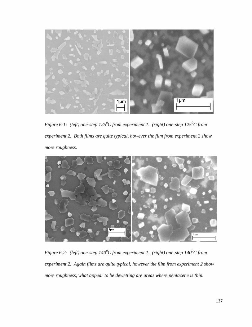
137
Figure 6-1: (left) one-step 1250C from experiment 1. (right) one-step 125
0C from
experiment 2. Both films are quite typical, however the film from experiment 2 show
more roughness.
Figure 6-2: (left) one-step 1400C from experiment 1. (right) one-step 140
0C from
experiment 2. Again films are quite typical, however the film from experiment 2 show
more roughness, what appear to be dewetting are areas where pentacene is thin.

138
The one-step TFT results are used as comparisons for the two-step results. C1 is
used to compare with experiment 1 and C2.1 is used for experiment 2. The results in C1
(figure 6.3) are typical and extremely clean. There is a peak in the mobility at
intermediate temperatures, and the mobility is the lowest at high temperatures. The
trends for the on/off ratio are the exact opposite to the mobility trend. The on/off ratio
was the highest at high temperatures and lowest at intermediate temperatures.
The results in C.2 (figure 6.4) had the same trends as C1, however the data is
extremely noisy. The mobility peak is at 1800C, instead of the typical 150-160
0C. The
on/off ratio was unusually high at low and high temperatures.

139
Figure 6-3: C1 TFT results (top) mobility (bottom) on/off ratio
4.16E-02
3.31E-02
6.43E-02 6.25E-02
2.69E-02
1.90E-02
0.00E+00
1.00E-02
2.00E-02
3.00E-02
4.00E-02
5.00E-02
6.00E-02
7.00E-02
8.00E-02
9.00E-02
120 130 140 150 160 170 180 190
Mo
bili
ty (
cm2/V
s)
Processing temperature (0C)
6.53E+01
2.35E+02
3.09E+01
7.31E+01
1.42E+03
7.46E+03
1.00E+00
1.00E+01
1.00E+02
1.00E+03
1.00E+04
120 130 140 150 160 170 180 190
on
/off
rat
io
Processing temperature (0C)
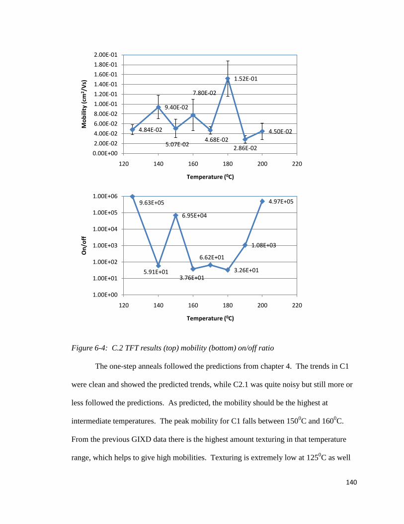
140
Figure 6-4: C.2 TFT results (top) mobility (bottom) on/off ratio
The one-step anneals followed the predictions from chapter 4. The trends in C1
were clean and showed the predicted trends, while C2.1 was quite noisy but still more or
less followed the predictions. As predicted, the mobility should be the highest at
intermediate temperatures. The peak mobility for C1 falls between 1500C and 160
0C.
From the previous GIXD data there is the highest amount texturing in that temperature
range, which helps to give high mobilities. Texturing is extremely low at 1250C as well
4.84E-02
9.40E-02
5.07E-02
7.80E-02
4.68E-02
1.52E-01
2.86E-02
4.50E-02
0.00E+00
2.00E-02
4.00E-02
6.00E-02
8.00E-02
1.00E-01
1.20E-01
1.40E-01
1.60E-01
1.80E-01
2.00E-01
120 140 160 180 200 220
Mo
bili
ty (
cm2/V
s)
Temperature (0C)
9.63E+05
5.91E+01
6.95E+04
3.76E+01
6.62E+01
3.26E+01
1.08E+03
4.97E+05
1.00E+00
1.00E+01
1.00E+02
1.00E+03
1.00E+04
1.00E+05
1.00E+06
120 140 160 180 200 220
On
/off
Temperature (0C)

141
as at 1800C, hence the mobility is lower as compared to the intermediate temperatures.
The mobility at 1250C is still higher than at 180
0C because once again from the GIXD
results, the crystallite size is smaller at 1800C as compared to 125
0C. From the SEM data
there is little dewetting at low temperatures as compared to high temperatures. Dewetting
causes the effective width of devices to decrease, causing an effective mobility drop.
From the data in C1 and C2.1, the on/off ratio and mobility seem to be inversely
proportional from each other. The on/off ratio is the lowest where the mobility is the
highest. At high temperatures the on/off ratio is the highest. Films processed at high
temperatures have the fewest defects as well as miscellaneous byproducts from the
precursor degradation giving the highest on/off ratio. In C1, the on/off ratio at low
temperatures is not particularly larger than at intermediate temperatures. The amount of
byproducts and defects at low temperatures keeps the on/off ratio relatively low. C2.1,
shows that there is the potential for extremely high on/off ratios at low temperatures,
however this data set is unusual. The high on/off at 1250C and 150
0C are anomalies.
It should be noted that evaporated pentacene is able to have mobility of greater
than 1cm2/V·s.
25 However, none of the transistors tested above have been able to reach
this high mobility. In fact no SAP -pentacene TFTs have been able to reach the high
mobility of pentacene TFTs with evaporated films. This is probably due to the
temperatures which are used to process SAP-pentacene films. Film must be heated above
1200C in order for the reverse Diels-Alder reaction to occur. It has been shown
pentacene films heated above 900C have lower mobility because the thin-film phase starts
relaxing to the bulk-like phase.26
As seen from the GIXD data in chapter 4, only a small
amount of the little thin-film phase of pentacene if formed on the high temperature films,
142
and no thin-film phase of pentacene is even detected at the lower temperatures. The
small amount of the thin-film phase is probably because since pentacene processing is
above 900C, the formation of the thin-film phase is not favorable. Fortunately some thin-
film phase is still present, to allow for the potential of high mobility.
Even though the formation of the high mobility thin-film phase is unfavorable, it
may still be possible to optimize these SAP-pentacene films utilizing a final high
temperature anneal is an attempt to fix defects and to drive off unwanted byproducts from
the sample. This is the reason for utilizing the post-processing anneal.
6.3.2 Post-processing anneal
Figure 6.5 shows the post-processing anneal series for films processed at 1250C
(125+160, 125+170, 125+180). No visual differences were noticed between films that
were processed with a final high temperature step versus films that were processed at
only one temperature from beginning to end. The SEM suggests that the final high
temperature anneal does not evoke large morphological changes. This makes sense,
because the final high temperature anneal was after the SAP to pentacene reaction has
already completed, there is no reason for anything drastic to happen after the film has
formed. The only possibility for a big visible film change is for pentacene to sublimate
away from the film, but this occurs at temperatures above 2000C.

143
Figure 6-5: 1250C films with post-processing anneal (top left) no anneal. (top right)
1600C anneal. (bottom left) 170
0C anneal. (bottom right) 180
0C anneal.
Figure 6.6, shows the TFT results for the post-processing anneal. For both the
mobility and the on/off ratio for films processed at 1500C, the different final anneals do
not produce statistically different results. In the 1500C heating series a final high
temperature anneal of any temperature does not change the performance of the pentacene
TFT. This is largely corroborates with the SEM data, showing that a final does not

144
produce any change. However, SEM by itself cannot confirm possible changes in crystal
structure and pentacene crystallite size. Only X-ray diffraction may be able to determine
the changes in crystallite size. Compared to the control samples, annealed films still
overall have a higher mobility, with no change in the on/off ratios.
For films processed at 1400C and 150
0C, results suggest that using a final high
temperature anneal also changes the mobility. The trend appears that a higher
temperature final anneal decreases the mobility while a lower temperature final anneal
increases the mobility. It is however, difficult to claim a statistical difference between
the 125+180 and 125+160 samples. What can be state conclusively is that, the highest
mobility devices in these two heating series have a higher mobility than the standard one-
step TFTs processed without the final anneal. Unfortunately, once again, the data show
an inverse relationship between mobility and on/off ratio. The good news is that the
lowest on/off values in the TFTs with the post-processing anneal over all exhibits higher
on/off than the one-step TFTs showing that the post-procesing anneal is able to improve
leakage.
Even though, the data does not conclusively state the effect of the final anneal
temperature, however it is clear that having a final anneal can give a boost in the final
mobility and there is an overall improvement the on/off ratio. In these series of tests only
short anneal times were tested, in the future, longer anneal times needs to be tested, and
changes in crystallite size needs to be confirmed.

145
Figure 6-6: Post-processing anneal. Each series of lines represent one heating series
(i.e. Samples with the same processing temperature, but different final anneal
temperature). (top) mobility (bottom) on/off ratio
6.3.3 Step-down Heating
For two-step heating samples, intermediate samples were made to check for
proper film development in between temperature steps. Figure 6.7 shows the formation
3.04E-01
3.56E-03
2.14E-01
2.78E-01
7.86E-02
7.92E-02
3.54E-01
3.01E-01
3.49E-01
0.00E+00
5.00E-02
1.00E-01
1.50E-01
2.00E-01
2.50E-01
3.00E-01
3.50E-01
4.00E-01
4.50E-01
155 160 165 170 175 180 185
Mo
bili
ty (
cm2/V
s)
Post-processing anneal temperature (0C)
125
140
150
1.00E+00
1.00E+01
1.00E+02
1.00E+03
1.00E+04
1.00E+05
1.00E+06
1.00E+07
155 160 165 170 175 180 185
on
/off
rat
io
Post-processing anneal temperature (0C)
125
140
150

146
of high temperature nuclei after processing at 1600C and 170
0C to form the high
temperature nuclei. The SEM images show proper formation of high temperature nuclei.
A the samples are fully processed with the step-down conditions the final films,
visually resemble one-step films which were processed at the higher temperature. For
example, as seen in figure 6.8, the 160-150, 160-140 and 160-125 films visually resemble
one-step 1600C films. The plateaus which are characteristic of films processed above
1500C were a defining feature in the entire step down films, showing that high
temperature characteristics were created using the two-step process.
Even though the films more closely resemble the higher temperature one-step
films, however, there were also some characteristics of low temperature processing. For
example, when comparing between samples in the 160 series (160-150, 160-140 and 160-
125), small pentacene islands between plateaus show up in samples 160-140 and 160-125
films. These small islands are typical of low temperature processing. There where more
islands in the 160-140 film compared to the 160-125 film, which is also a trend seen in
low temperature processing. Furthermore, the amount of dewetting decreases as the
second heating step temperature decreases. As seen in figure 6.8, sample 160-125 had
less dewetting than sample 160-150, this again followed the trends seen in chapter 4. All
the trends decscribed for the160 series where true for all the other sample series as well.
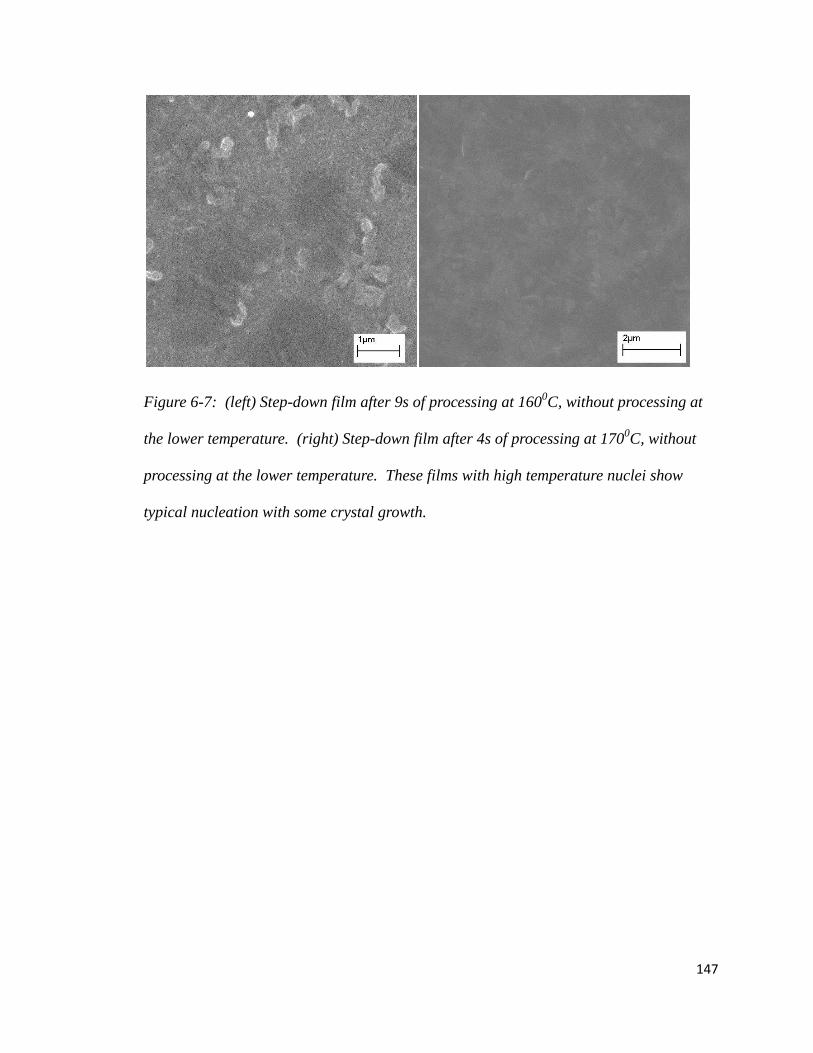
147
Figure 6-7: (left) Step-down film after 9s of processing at 1600C, without processing at
the lower temperature. (right) Step-down film after 4s of processing at 1700C, without
processing at the lower temperature. These films with high temperature nuclei show
typical nucleation with some crystal growth.

148
Figure 6-8: (top left) One-step 1600C film. (top right) Step-down 160-125. (bottom left)
Step-down 160-140. (bottom right) Step-down 160-150.
TFT measurements for step-down experiments showed a clear mobility trend
(figure 6.9). For samples with the same nucleation temperature, the mobility increases
with increasing crystal growth temperature. The mobility drop comes from the increased
number of nuclei which forms when high nucleation temperatures are used. The
increased number of nuclei decreases the pentacene crystal size and would account for a
decrease in mobility.

149
On the other hand, when the nucleation temperature is fixed and the
crystallization temperature changes, mobility increases for higher crystal growth
temperatures. It was originally thought that the 160-125 sample would give the highest
mobility, since at 1600C the texturing is the highest, and the low crystal growth
temperature would grow large pentacene crystals. However, using 1250C consistently
gave the lowest mobility for each heating series. The low mobility for the 1250C crystal
growth can probably be attributed to the loss of texturing when the low temperature
crystallization is used. So even with the high temperature nuclei, the crystals which grow
above the intial nuclei are probably still relatively disordered. A good guess would be
that the step down films should be more textured than a film processed exclusively at a
the low crystal grwth temperature, but less textured than a film processed exclusively at a
the high nucleation temperature. Furthermore, even though a low temperature is used in
order to promote crystal growth, the increased number of starting nuclei would probably
make the final crystal size smaller than film growth exclusively at the low crystal growth
temperature. These two factors contribute to the decreased mobility from a low
crystallization temperature. However, when compared with single step films, the best
step-down films are able to achieve higher mobility than one-step films.
The trends for on/off ratio were not quite as clear. For all heating series, using the
highest crystal growth temperature (1500C) gave the best on/off ratio. However, the on
off ratio was higher when the crystal growth temperature was 1250C versus 140
0C, albeit
both at 1250C and 140
0C, the on/off ratios were significantly lower than at 150
0C. When
the nucleation temperature was reduced the the on/off ratio also decreased.

150
Again, just as with mobility, the highest step-down on/off ratio exceeded the one-
step on/off ratios. Unlike the control set however, mobility and on/off ratio are not
inversely proportional to each other.
Figure 6-9: Step-down heating. Each series of lines represent one heating series (i.e.
Samples with the same nucleation temperature). (top) mobility (bottom) on/off ratio
The goal of the step-down experiments was attempt to get the best of both worlds,
by using a high temperature nucleation should leads to a textured film, but using a low
3.72E-02 8.10E-02
2.16E-01
2.01E-02 4.15E-02
1.18E-01
8.48E-031.38E-02
1.08E-01
0.00E+00
5.00E-02
1.00E-01
1.50E-01
2.00E-01
2.50E-01
3.00E-01
120 125 130 135 140 145 150 155
Mo
bili
ty (
cm2 /
Vs)
Temp 2-Crystal growth temperature (0C)
160
170
180
3.69E+02 6.76E+02
7.00E+045.27E+03
5.21E+01
1.32E+06
2.16E+04 2.61E+03
5.41E+06
1.00E+00
1.00E+01
1.00E+02
1.00E+03
1.00E+04
1.00E+05
1.00E+06
1.00E+07
120 125 130 135 140 145 150 155
on
/off
rat
io
Temp 2-Crystal growth temperature (0C)
160
170
180

151
temperature for crystal growth should promote large crystallite sizes and decrease
dewetting, all these factors should allow for films with higher mobility compared with
one-step processed films. The greatest benefit seen in the step-down films is the high
mobility along with high on/off ratios. These films give mobility higher than one-step
films as well as on/off ratios larger than the one-step films. The previously seen inverse
relationship between on/off ratios and mobility is broken. On again the sweet spot for
high performance occurs in the 1500C-160
0C. This can probably be explained by
postulating that nucleating at 1600C, allows for highly textured high temperature
nucleation, but the crystal growth at 1500C gives larger crystal than processing purely at
1600C, however the crystals are still textured as compared to crystal growth at 125
0C
lower temperature. This however needs to be tested with X-ray diffraction. Furthermore,
only a limited set of step-down conditions have been tested, a wider range of step-down
conditions also needs to be tested.
6.3.4 Step-up results
For step-up films there were no great visual differences between each series.
Figure 6.10 shows, the step-up series for 1250C. The step-up film more closely
resembles a one-step film processed at the lower temperature.

152
Figure 6-10: (top left) one-step 1250C. (top right) step-up 125-160. (bottom left) step-
up 125-170. (bottom right) step-up 125-180.
No clear trends can be seen in the step-up results (figure 6.11). This set of TFTs
came from experiment 2, where there was a great deal of noise in the control, which
indicates that there is great deal of noise in all the TFTs in experiment 2, therefore the
results may be hidden in the noise. Nonetheless, the highest mobilities and on/off ratios
in the step-up experiments exceed the highest mobilities and on/off ratios in C2.1.
Unfortunately, high mobility also corresponded to low on/off ratios.

153
Figure 6-11: Step-up heating. Each series of lines represent one heating series (i.e.
Samples with the same nucleation temperature). (top) mobility (bottom) on/off ratio
Step-up films, look like the one-step films processed at the lower temperature.
However, the step-up films may have smaller crystallite sizes than one-step films. This
still needs to be confirmed with x-ray diffraction.
TFTs with step-up processing, showed no clear trends. Overall, mobility were
higher than the one-step TFTs. The step-up films being subject to a final high
3.04E-01
1.14E-03
1.75E-01
2.57E-01
4.55E-02
2.82E-022.73E-02
3.58E-01
2.89E-01
0.00E+00
5.00E-02
1.00E-01
1.50E-01
2.00E-01
2.50E-01
3.00E-01
3.50E-01
4.00E-01
4.50E-01
155 160 165 170 175 180 185
Mo
bili
ty (
cm2/V
s)
Crystal growth temperature (0C)
125
140
150
6.45E+01
1.46E+06
8.37E+019.06E+01
3.41E+06
5.79E+01
3.70E+06
1.40E+02
4.16E+01
1.00E+00
1.00E+01
1.00E+02
1.00E+03
1.00E+04
1.00E+05
1.00E+06
1.00E+07
155 160 165 170 175 180 185
on
/off
Crystal growth temperature (0C)
125
140
150

154
temperature step may have received the same benefits as films with a post-processing
anneal, overall giving s boost in mobility and the on/off ratio. The inverse
proportionality between mobility and on/off however is still present.
6.3.5 Quenching Control (C2.2)
The results of C2.2 consists of a repeat of the 1600C step-down series, as well as a
step down, where the second temperature remains at 1600C. The 160-150, 160-140 and
160-125 samples are consistent with the step-down result from experiment 1. The 160-
160 control sample had the small pentacene islands between the pentacene plateaus,
resembling the 160-140 film instead of the one-step 1600C film. This shows that the 160-
160 film is not identical to the one-step 1600C. The cool down and reheat clearly has a
significant effect to the processing of pentacene films.
Figure 6-12: (left) One-step 1600C film. (right) 160-160 film. The 160-160 film has
small pentacene island characteristic of films processed at lower temperatures.

155
Figure 6.13 shows the results for the TFT quench control experiment. C2.2 was
measured mainly to check the results the effects of cooling and reheating during
pentacene film processing. The data point of most interest was the reheat back 1600C.
There seems to be a significant increase in mobility and on/off ratio as compared to the
single step 1600C measurement. For the rest of the data points were repeats of the 160
0C
step-down heating series. The data follows the trend seen above in the full step-down
data set. Mobility and on/off ratio both decreases as crystallization temperature
decreases.

156
Figure 6-13: Quench control. (top) mobility (bottom) on/off ratio
The data from C2.2, is important in determining the effects of cool down and
reheat in the step-up experiments. Clearly the cool down and reheating did not produce
films identical to one-step 1600C film. The final film visually resembles 160-140 films,
showing that Diels-Alder reaction cannot be instantly quenched nor can it be instantly
restarted at the high temperature. Instead, as the film reheats, there is crystal growth
below the desired temperature, because films cannot instantly jump from one temperature
1.51E-01
2.16E-01
8.01E-02
9.22E-02
0.00E+00
5.00E-02
1.00E-01
1.50E-01
2.00E-01
2.50E-01
3.00E-01
120 130 140 150 160 170
Mo
bili
ty (
cm2/V
s)
Crystal growth temperature (0C)
6.36E+01
7.00E+04
4.95E+01
9.83E+01
1.00E+00
1.00E+01
1.00E+02
1.00E+03
1.00E+04
1.00E+05
120 130 140 150 160 170
on
/off
rat
io
Crystal growth temperature (0C)

157
to another via the crude techniques employed. A few seconds pass before the film is
reheated to the set temperature. Therefore, the 160-160 control sample is not the same as
the one-step sample. This may not necessarily be an issue for the step-down films,
however may be an issue for step up films
Considering the C2.2 data the cool down and reheat used for the step-up film may
play a significant role in the final film. None of the step-up films may truly step-up
films, since significant crystal growth takes place at temperatures lower than the desired
crystal growth temperature. In order to prevent problems of cooling and reheating, a
heating system with quick temperature response would be necessary for future
experiments.
6.4 Conclusions
It is quite clear from the SEM result, that the appearance of the final film is
largely determined by the type nuclei formed in the early parts of film development. The
nuclei type is determined by the initial processing temperature, making the initial
processing temperature the most important part of SAP-pentacene film formation. In
both the step-up and step-down films, the film appearance is closer to a one step-film
processed at the nucleation temperature of the two-step film. This indicates that, as
expected, nucleation is more energetically intensive than crystal growth. As seen in
chapter 4, the nucleation density does not increase as the Diels-Alder reaction proceeds.
Once the nuclei are formed, it is more favorable for crystals to grow than for new nuclei
to form.
Even though in two-step processing the films is most affected by the starting
temperature, however in the case of the step-down film both high temperature and low
158
temperature features appear in the final film, with high temperature feature being the
most dominant. The identification of pentacene morphotypes and crystallite size is
unknown. This can only be determined through X-ray diffraction. Most likely, even
though the final film resembles the one-step film, however, because crystal growth
temperatures is different from the one-step film, the crystallite sizes are different. In the
case of step-down films, the crystal sizes should larger than the one-step films because
crystals are allowed to grow slowly. In the step-up films, the crystals should be smaller
than one-step films because of the fast crystal growth.
Three types of heat-treatments have explored, and data suggest that using multiple
heating steps for a precursor system is beneficial. Only a limited number of heat-
treatments have been tested, but many more heat-treatments can be tried and tested. One
simple extension of what has already been tried, is to vary the post-processing anneal
time. The current data suggests that a step-down film with a post-processing anneal
might be able to give the best mobilities and on/off ratios, this also has not been tested.

159
6.5 References
1. Song, C. et al. Characteristics of pentacene organic thin film transistors with gate
insulator processed by organic molecules. JAPANESE JOURNAL OF APPLIED
PHYSICS PART 1-REGULAR PAPERS SHORT NOTES & 41, 2730-2734(2002).
2. Mun, S. et al. Determining the optimum pentacene channel thickness on hydrophobic
and hydrophilic dielectric surface. APPLIED PHYSICS LETTERS 93, (2008).
3. Shtein, M. et al. Effects of film morphology and gate dielectric surface preparation on
the electrical characteristics of organic-vapor-phase-deposited pentacene thin-film
transistors. APPLIED PHYSICS LETTERS 81, 268-270(2002).
4. Lee, M. & Song, C. Oxygen plasma effects on performance of pentacene thin film
transistor. JAPANESE JOURNAL OF APPLIED PHYSICS PART 1-REGULAR
PAPERS SHORT NOTES & 42, 4218-4221(2003).
5. Lim, S. et al. Surface-treatment effects on organic thin-film transistors. SYNTHETIC
METALS 148, 75-79(2005).
6. Salih, A. et al. Improved thin films of pentacene via pulsed laser deposition at
elevated substrate temperatures. APPLIED PHYSICS LETTERS 69, 2231-
2233(1996).
7. Gundlach, D. et al. Pentacene organic thin-film transistors - Molecular ordering and
mobility. IEEE ELECTRON DEVICE LETTERS 18, 87-89(1997).
8. Park, J. et al. Characteristics of pentacene-based thin-film transistors. MATERIALS
SCIENCE & ENGINEERING C-BIOMIMETIC AND SUPRAMOLECULAR
SYSTEMS 24, 27-29(2004).

160
9. Choi, J. et al. Electrical characteristics of pentacene organic thin film transistors with
silicon dioxide gate insulator. MOLECULAR CRYSTALS AND LIQUID CRYSTALS
349, 339-342(2000).
10. Yagi, I., Tsukagoshi, K. & Aoyagi, Y. Growth control of pentacene films on SiO2/Si
substrates towards formation of flat conduction layers. THIN SOLID FILMS 467,
168-171(2004).
11. Bouchoms, I. et al. Morphology identification of the thin film phases of vacuum
evaporated pentacene on SIO2 substrates. SYNTHETIC METALS 104, 175-
178(1999).
12. Lee, J. et al. 10-nm channel length pentacene transistors. Electron Devices, IEEE
Transactions on 52, 1874-1879(2005).
13. Fritz, S.E., Kelley, T.W. & Frisbie, C.D. Effect of Dielectric Roughness on
Performance of Pentacene TFTs and Restoration of Performance with a Polymeric
Smoothing Layer. The Journal of Physical Chemistry B 109, 10574-10577(2005).
14. Gundlach, D. et al. Pentacene organic thin-film transistors-molecular ordering and
mobility. Electron Device Letters, IEEE 18, 87-89(1997).
15. Guo, D., Ikeda, S. & Saiki, K. Pentacene films grown on surface treated SiO2
substrates. Thin Solid Films 515, 814-817(2006).
16. Steudel, S. et al. 50MHz rectifier based on an organic diode. NATURE MATERIALS
4, 597-600(2005).
17. Voz, C. et al. Optoelectronic devices based on evaporated pentacene films. Solar
Energy Materials and Solar Cells 87, 567-573(2005).

161
18. Gui-Fang, D. et al. Improvement of Performance of Organic Thin-Film Transistors
through Zone Annealing. Chinese Physics Letters 22, 2027-2030(2005).
19. Kang, S.J. et al. Influence of postannealing on polycrystalline pentacene thin film
transistor. J. Appl. Phys. 95, 2293-2296(2004).
20. Tunnell, A. et al. Printing-induced improvements of organic thin-film transistors.
Organic Electronics 9, 507-514(2008).
21. Sung Kyu Park et al. High-performance polymer tfts printed on a plastic substrate.
Electron Devices, IEEE Transactions on 49, 2008-2015(2002).
22. Yong-Hoon Kim, Dae-Gyu Moon & Jeong-In Han Organic TFT array on a paper
substrate. Electron Device Letters, IEEE 25, 702-704(2004).
23. Kline, R.J. et al. Significant dependence of morphology and charge carrier mobility
on substrate surface chemistry in high performance polythiophene semiconductor
films. Appl. Phys. Lett. 90, 062117-3(2007).
24. Coriolis, E.G.D. & Cowan, R.J. Effect of Atmospheres on the Heat Treatment of
Metals. Industrial & Engineering Chemistry 21, 1164-1168(1929).
25. Lin, Y. et al. Stacked pentacene layer organic thin-film transistors with improved
characteristics. Electron Device Letters, IEEE 18, 606-608(1997).
26. Ji, T., Jung, S. & Varadan, V.K. On the correlation of postannealing induced phase
transition in pentacene with carrier transport. Organic Electronics 9, 895-898(2008).

162
7 Conclusions and Suggestions for Future Work
This work predominantly focused on the formation of pentacene thin films
through a precursor system. The reason for using pentacene is because of the potential
high mobility promised by this particular semiconductor which rivals the performance of
amorphous silicon. Unfortunately the performance of pentacene processed from
precursors fall short in performance and is not as high as reported mobility from
evaporated pentacene. However, in order to achieve the goals of low-cost electronics,
solution processing required and the pentacene precursor still reports one of the higher
mobility among solution processable organic semiconductors. In order gain more insight
on proper processing of SAP pentacene precursor, a thorough study of the thin film
growth mechanisms of SAP to pentacene was performed. The growth mechanism was
further tested on various surfaces which are relevant to printed electronics. Finally,
electrical performance of pentacene TFTs from SAP was tested using different heat
treatment in order to optimize pentacene film to achieve high performance. There is still
more work which still can be done in the study of precursor semiconductors for OTFTs.
The study of SAP conversion to pentacene started in chapter 3 with a purely
quantitative chemical analysis of the conversion using UV-vis spectroscopy. The
degradation rate of SAP was measured at various temperatures and was extracted by
looking at the appearance the 667nm peak. In a solid-state reaction the reaction many
times is usually in a sigmoidal shape. In the degradation of SAP, the reaction was

163
properly described by a decaying exponential. This indicates that the conversion of SAP
to pentacene is the energetically most expensive step in film formation. It should then be
expected that the mechanisms of film formation would be reaction rate dependent. The
most important aspect of the degradation rate extraction that now the reaction rate can be
used to gauge reaction completion when processing with SAP, which is something which
is fundamental, but previously unknown.
Chapter 4, focuses on the understanding of pentacene thin film formation on
oxide from SAP. The study found two temperature dependent nuclei. A low temperature
nuclei promoted island like growth of films and a high temperature nuclei promoted a
layer by layer smooth film growth. The formation of these two types of nuclei was a
result of the reaction rate. The island like nuclei forms the bulk-like phase of pentacene.
This is the relaxed phase of pentacene and forms due to the slow precursor reaction
causing the supply of pentacene molecules for crystal formation to be slow promoting
large relaxed crystal. This also decouples crystal interacts with the substrate and
resulting films are largely untextured. The high temperature monolayer nucleus forms
because of the fast SAP reaction rate at high temperatures. This causes a quick
condensation of pentacene, forming the unstable thin-film phase of pentacene. This
phase of pentacene caused the resulting film to be highly textured. However, extremely
high temperatures, the rapid development of nuclei causes film texturing to be slowly lost
and crystals to be small. Based on this study, it can be predicted that when SAP is
processed at intermediate temperatures, the presence of texturing and relatively large
crystals would give the highest mobility for pentacene TFTs.

164
Chapter 5 continues to describe pentacene thin film growth on five other
substrates, all of which are important for organic electronics, PEDOT on gold, PVP, gold,
silver, HMDS on oxide and oxide. Each substrate has a different energetic interaction
with pentacene, which would cause pentacene interactions to be more favorable or less
favorable. By using the amount of dewetting of pentacene films from the substrate a
quick estimate of pentacene stability on the substrate can be measured. As expected, the
metallic substrate offered the least stability showing the most dewetting of pentacene
form substrate surfaces and organic substrates showed the highest stability with the least
pentacene dewetting. The nucleation density of pentacene was found to be constant
across all the different substrates. The lateral dimensions of pentacene islands were also
constant across the board showing again. This study showed that during the initial stages
of film formation, the substrate does not play a significant energetic effect on pentacene
film formation, instead the precursor matrix is energetically more important. At the latter
part of film formation when the precursor is largely consumed, the substrate starts to play
a larger role on the film formation. The substrate interaction then determines the
roughness of the pentacene films. The roughest films are the films with unstable
interactions with the substrates. The smoothest films are the films grown on substrates
which have a stable interaction with pentacene.
Chapter 6 finally describes electrical performance of pentacene TFTs. In this
chapter using the knowledge gain from the previous chapters, heat-treatments of the SAP
conversion was tested in order to optimize electrical performance on TFT films. TFTs
processed at a single temperature followed the predictions from chapter 4. Films
processed at intermediate temperatures showed the best mobility because of the presence

165
of the thin-film phase of pentacene as well as high texturing and low film dewetting.
TFTs processed at low temperatures showed low performance due to high disorder of the
pentacene crystal orientation. TFTs processed at high temperatures also showed low
mobility due to small crystal sizes, high dewetting and loss of film texturing.
Furthermore, three different two temperatures SAP processes where tested in TFT
fabrication. First, TFTs were made in the standard single temperature heating, but a short
high temperature anneal was added after the film was fully processed. This study showed
an overall increase in the on/off ratio, since a high temperature anneal is able to fix
defects in pentacene crystals. Next, films were made with the step-down processing
where, nucleation is initialed at a high temperature and then crystals are grown and films
formed at a lower temperature. This process attempts to create films which are well
ordered and have large crystal sizes, which should give mobility higher than standard
single temperature processing. The step-down process showed the most promise.
Mobility was increased simultaneously with the on/off ratio give high performance and
low leakage. Finally, the step-up process, which the opposite of the step-down process,
was tested and it showed few trends and few conclusion were able to be made. The SEM
studies of film growth using these heat treatments showed that the final film morphology
is largely determined by film nucleation. Since regardless of the final temperature used
to process films, the final film always looks more like films processed exclusively at the
nucleation temperature. The use of heat treatments in the processing of semiconducting
precursors is promising, because it allows for fine control in order to improve the
performance of pentacene TFTs which would hopefully allow for precursor pentacene
TFTs to reach the performance of evaporated pentacene TFTs.

166
The motivating factor of this thesis was the solution processing of organic
semiconductors for low-cost electronics. In creating low-cost electronics TFTs are an
important component to the realization of this goal. However other devices also need to
be made. One particularly elusive device is a solution processed diode. To date no group
has been able to report a fully solution processed diode. Many fully evaporated diodes
have been reported, even diodes which function well at high frequencies.1,2
The
pentacene precursor used in this study would be a good choice for use in a solution
processed diode. However, the requirements for the pentacene to be incorporated into a
diode are largely different than when used in a TFT. The processing of the pentacene
precursor for such a device may be completely different than what has been reported in
this thesis. For the realization of such a device different considerations need to be taken.
The processing of the SAP pentacene precursor for a solution processed diode can be a
direction for future work.
In conclusion, the formation of pentacene films from SAP has now been explored
in great detail and better understood after this study. This knowledge allows for the
optimization of the performance of solution processed TFTs using SAP-pentacene.
These results may serve as a model semiconducting precursors which may be made in the
future.

167
7.1 References
1. Steudel, S. et al. 50MHz rectifier based on an organic diode. NATURE MATERIALS 4,
597-600(2005).
2. Steudel, S. et al. Comparison of organic diode structures regarding high-frequency
rectification behavior in radio-frequency identification tags. JOURNAL OF APPLIED
PHYSICS 99, (2006).

168
9 Appendix (SAP synthesis)
9.1 Introduction
This pentacene precursor, was developed by Afzali, et al.1 and modified by
Steven Volkman.2 Until recently, SAP was only available by in house synthesis, now it
available through Aldrich by special order.
9.2 Chemicals Required
Pentacene C22H14
N,O-Bis(trimethylsiyl)-acetamide CH3C[=NSi(CH3)3]OSi(CH3)3
Thionyl Chloride Cl2OS
Methyltrioxorhenium(VII) CH3ReO3
Chloroform CHCl3
Hexanes C6H14
Ethyl Acetate C4H8O2
Dry Ice CO2
9.3 Laboratory Equipment
Sublimation Tube (Quartz)
Sublimation Heater System (3 zones with thermocouples and controllers)
Forming Gas Cylinder
Mass Flow Controller and Valve
Vacuum Pump

169
Bunsen Burner
250 mL Round Bottom Flask
Distillation Apparatus
100 mL Round Bottle
Schlenk Flask
Hot Air gun
50 mL Round Bottom Flask
Glass Reflux Tube for 50 mL Round Bottom Flask
Magnetic Stir Bar and Stirrer
High-Frequency Sound Wave Generator
2000 mL Erlenmeyer Flask
Glass Column
Reservoir
Silica Glass
Silica Gel
Ultra Violet Light Source
9.4 Overview
SAP synthesis is split up into 3 sections. First, pentacene is purified by
sublimation using a three zone sublimating tube. Second, the Diels-Alder adduct is
made. Lastly, is the Diels-Alder reaction, attaching the adduct to the pentacene molecule.

170
9.5 Pentacene Sublimation Purification
9.5.1 Preparation
Thoroughly clean a quartz tube using acetone and IPA
Dry the quartz tube with a nitrogen gun
Thoroughly dry the quartz tube and burn off all organic contaminants by baking the
tube in sublimation heater for 3 hours under vacuum and nitrogen at 3000C.
Cool the furnace and quartz tube to room temperature.
9.5.2 Sublimation
Warm pentacene up to room temperature. (Pentacene is stored in the freezer. Do not
open the bottle until the pentacene is sufficiently warm to prevent condensation on to
the pentacene. Pentacene is supplied from TCI)
Place all of the pentacene ~1g into one end of the quartz tube. ~1 cm from the edge
of the quartz tube. Try to keep the pentacene concentrated in a small region.
Place the quartz tube into the sublimation heater, pentacene end first. Make sure the
pentacene is in 1st heating zone of the heater.
Bring the heater under vacuum and nitrogen condition. The mass flow controller
should be set to 3.5 ccm/min flow.
Set the 1st zone to 260
0C, the 2
nd zone to 190
0C, the 3
rd zone to 160
0C. Heat for ~48
hours, or until zone one has no more pentacene. There should be some black residual
impurities.
Cool heater and tube to room temperature.
Using acetone clean off impurities in zone one.

171
Scrape out the pentacene from zone 2 and half of zone 3.
Weigh the pentacene. (Yield should be at least 70%-80%)
Seal the pentacene in a glass vial and store it in the freeze.
9.6 Diels-Alder Adduct synthesis (NSO)
9.6.1 Preparation
Clean all necessary glassware. Dry all glassware overnight in an oven. (Make sure
the oven is set over 1000C)
Right before the reaction
Seal a magnetic stir bar in a 250mL flask with a rubber septum. Fill the flask with
nitrogen (make sure to have a syringe outlet). Flame dry the flask to thoroughly dry
the flask, with the nitrogen constantly flowing. This creates a dry oxygen free flask.
(Standard flame dry procedures require three heat and cool cycles.)
Flame dry the schlenk flask, and fill it with nitrogen.
9.6.2 Synthesis
Add 20 mL of N,O-Bis(trimethylsiyl)-acetamide into the flask through the septum.
Use oxygen free techniques to make the acetamide does not get contaminated.
Add 8 mL of thionyl chloride into the flask. (Add drop by drop, this should take
over 20 minutes. Adding the thionyl chloride too quickly makes the solution boil,
which is undesireable.)
Setup the distillation apparatus. Setup the nitrogen to flow nitrogen into the
apparatus. Also setup the vacuum. Use a two way value so that the apparatus can be

172
switched back an forth between vacuum and nitrogen. Flow nitrogen into the
apparatus.
Once the set up is sufficiently cool, attach the NSO filled 250mL flask onto the
source side of the apparatus. Attach a 100 mL round bottom flask to the waste side of
the apparatus. Flow water through the condensation region.
Place a crystallization dish with dry ice and acetone under the waste flask.
Slowly bring the apparatus under vacuum. The NSO may start to bubble, in which
case, switch back to nitrogen. Repeat this process until the NSO no longer bubbles
under vacuum. Keep the setup under vacuum.
Slowly apply heat using a hot air gun to the flask and the vertical column. The NSO
may start to boil, in which case stop heating. The goal is to heat and evaporate the
liquid without boiling. A clear liquid will start to collect in the waste flask, the waste
may crystallize. Continue to heat until the waste is no longer clear but yellow. The
yellow is desired product and is no longer waste.
Fill the setup with with nitrogen and remove the waste flask and replace it with the
dry schlenk flask. Work quickly to keep the setup oxygen free. The NSO product is
oxygen sensitive. Bring the setup back down to vacuum.
Apply heat to the NSO flask in the same fashion as above. Heat until the flask is
completely dry. Black byproducts will be left in the flask. Bring the setup to
nitrogen. Seal the schlenk flask and remove it from the setup. Cover the flask with
aluminum and store it in a freezer. The NSO compound should be yellow, if it trn
reddish brown, the product has reacted with oxygen. There will be enough NSO for
several reactions. If oxygen free procedures are followed correctly, the NSO should

173
be able to be stored for months.
9.7 Diels-Alder Reaction (SAP synthesis)
9.7.1 Preparation
Clean and oven dry all glassware before hand.
Before starting the reaction make an dry, oxygen free 50 mL round bottom flask, with
a magnetic stir bar sealed inside.
9.7.2 Synthesis
Bring the NSO and the purified pentacene out of the freezer. Allow to be warmed up
to room temperature before use.
Setup the reflux tube, along with water running through the sleeve. Setup the
nitrogen and vacuum to a two way valves and flow nitrogen into the reflux tube.
Place the round bottom flask on ring stand over stirrer and add 15 mL of anhydrous
chloroform, using oxygen free techniques.
Weigh the pentacene, then weigh out the proper mole ratio of catalyst (Table A.2).
Add both pentacene and catalyst into the flask. This requires the flask to be opened,
so work quickly. Once the chemicals are added, flow nitrogen through the flask again
to exlude oxygen.
Sonicate this mixture for 1-3 minutes to remove large pentacene flakes.
Add the proper mole ratio of NSO (Table A.2) using a long needle and syringe.
Connect the flask to the reflux tube.

174
Slowly bring the setup to vacuum. Once again, the chloroform will bubble, in which
case, bring the setup back to nitrogen. Go back and forth between vacuum and
nitrogen for at least ten times. Finally, bring the setup to nitrogen at the end.
Heat the round bottom flask with a mineral bath at 71-720C, make sure that the oil
covers the solvent. Heat for 7 hours at 71-720C. The final product in the flask will
look dark. Make sure the solvent does not dry out. This is done by controlling the
nitrogen flow through the manifold.
9.8 SAP purification
9.8.1 Preparation
Clean all necessary glassware before starting
Prepare the chromatography solutions before hand: 1 4L bottle of 20% ethyl acetate
+ 80% hexanes (20/80 solution) and 2 4L bottle of 30% ethyl acetate + 70% hexanes
(30/70 solution).
9.8.2 Flash Column Purification
Using a 2L Erlenmeyer flask, mix silica gel with 20/80 solution. Make sure the silica
gel is solvated. Pack the column using standard techniques. Make sure the silica gel
stays solvated. The packed column should be approximately 2/3 full.
Allow the excess solution to flow out of the column, but making sure the top of the
silica gel does not dry out.
Load the column with precursor. Make sure to form a smooth, even layer on the top
of the silica gel.

175
Fill the rest of the column with 20/80 solution being careful not to disrupt the
precursor layer.
Attach the reservoir and continue to fill the setup with 20/80 solution.
Start running the column, using high pressure for the column to flow faster.
Fill the reservoir as needed. Use up the 20/80 solution.
Now switch to the 30/70 solution.
Once the solvent is switch, start collecting samples, 500mL
Use TLC to monitor the product.
Discard all collected samples without the product.
Using a rotary evaporator, collect the desired product.
Dissolve the product with chloroform, and transfer it into a vial.
Using the rotary evaporator, dry off the chloroform.
Wash the product with hexanes by adding hexanes into the vial and mixing the
product around. Centrifuge the vial and remove the hexanes. Do this at least three
times.
Finally dry off the hexane using the rotary evaporator. Store the product in the
freezer.
The final product should colorless, however, a yellow or orange color is also
acceptable.

176
Chemical Formula MW
(amu)
Mp
(°C)
Bp
(°C)
d
(g/mL) Pentacene C22H14 278.34 -- -- --
N,O-Bis(trimethylsinyl)-
acetamide
CH3C[=NSi(CH3)3]OSi(C
H3)3
203.43 24 71-73 0.832
Thionyl Chloride Cl2OS 118.97 -105 78-79 1.635
Methyltrioxorhenium(VII) CH3ReO3 249.23 111 -- --
Chloroform CHCl3 119.38 -64 62 1.498
Hexanes C6H14 86.18 -95 69 0.659
Ethyl Acetate C4H8O2 88.12 -84 77 0.895
Table 9-1 Chemicals Properties of Chemicals
Chemical Formula MW (amu) Density (g/mL) Molar ratio
Pentacene C22H14 278.34 -- 1.0
NSO C2NO2SH3 105.2 1.327g/mL 1.5
Methyltrioxorhenium(VII) CH3ReO3 249.23 -- 0.01
Table 9-2: Mole ratios for Diel-Alder reaction

177
9.9 References
1. Afzali, A., Dimitrakopoulos, C. & Breen, T. High-performance, solution-processed
organic thin film transistors from a novel pentacene precursor. JOURNAL OF THE
AMERICAN CHEMICAL SOCIETY 124, 8812-8813(2002).
2. Volkman, S. et al. Inkjetted organic transistors using a novel pentacene precursor.
MRS Proceedings H11.7(2003).