Embed Size (px)
Citation preview

1
1
EE143 – Fall 2016Microfabrication Technologies
Lecture 6: Thin Film DepositionReading: Jaeger Chapter 6
Prof. Ming C. Wu
511 Sutardja Dai Hall (SDH)
2
Vacuum Basics
• Units– 1 atmosphere = 760 torr = 1.013x10⁵ Pa– 1 bar = 105 Pa = 750 torr– 1 torr = 1 mm Hg– 1 mtorr = 1 micron Hg – 1 Pa = 7.5 mtorr = 1 newton/m2– 1 torr = 133.3 Pa
• Ideal Gas Law: PV = NkT– k = 1.38E-23 Joules/K
= 1.37E-22 atm cm3/K– N = # of molecules (note the typo in your book)– T = absolute temperature in K

2
3
Dalton’s Law of Partial Pressure
• For mixture of non-reactive gases in a common vessel, each gas exerts its pressure independent of others
• 𝑷𝒕𝒐𝒕𝒂𝒍 = 𝑷𝟏 + 𝑷𝟐 +⋯ .+𝑷𝑵– Total pressure = Sum of partial pressures
• 𝑵𝒕𝒐𝒕𝒂𝒍 = 𝑵𝟏 + 𝑵𝟐 +⋯ .+𝑵𝑵– Total number of molecules = sum of individual molecules
• Ideal gas law observed by each gas, as well as all gases– 𝑷𝟏𝐕 = 𝑵𝟏𝒌𝑻– 𝑷𝟐𝐕 = 𝑵𝟐𝒌𝑻– 𝑷𝑵𝐕 = 𝑵𝑵𝒌𝑻
4
Average Molecular Velocity
• Assumes Maxwell-Boltzman Velocity Distribution
𝒗3 =𝟖𝒌𝑻𝝅𝒎
�
• where m = molecular weight of gas molecule
3
5
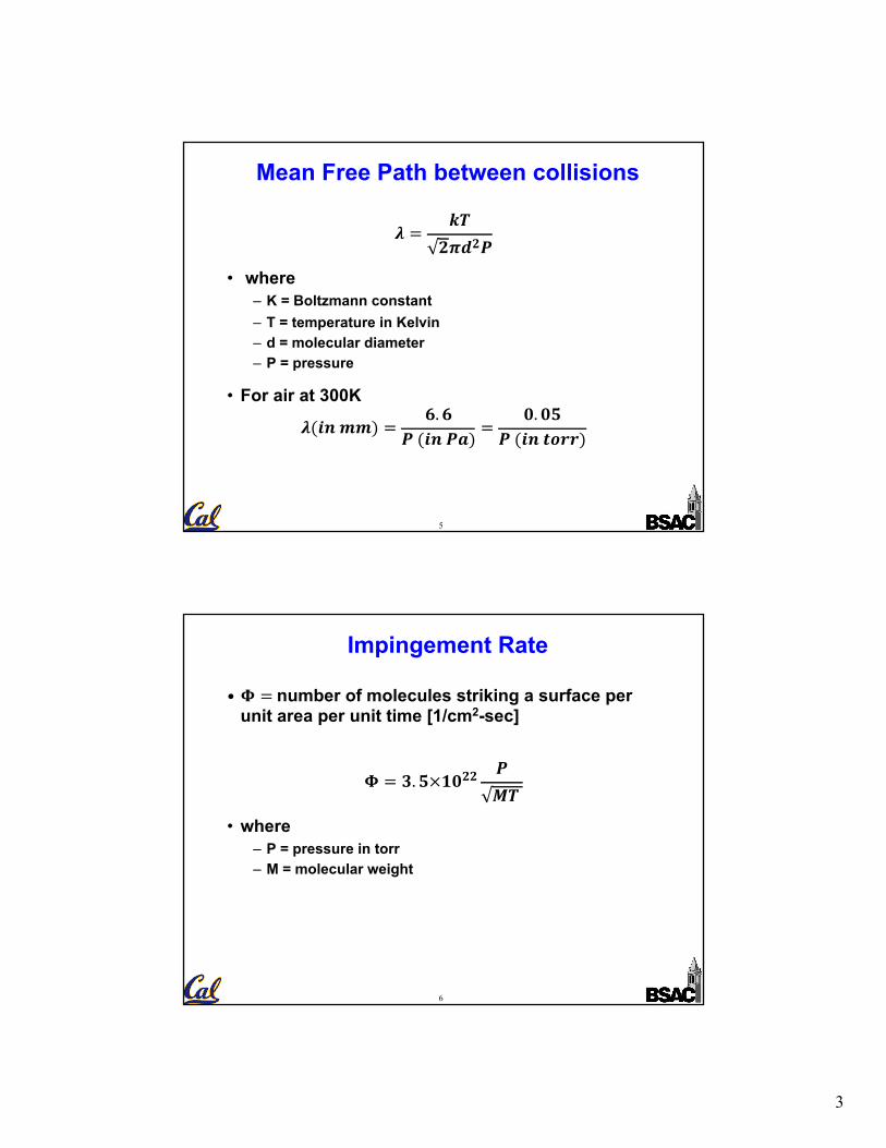
Mean Free Path between collisions
𝝀 =𝒌𝑻𝟐� 𝝅𝒅𝟐𝑷
• where – K = Boltzmann constant– T = temperature in Kelvin– d = molecular diameter– P = pressure
• For air at 300K
𝝀(𝒊𝒏 𝒎𝒎) =𝟔. 𝟔
𝑷 (𝒊𝒏 𝑷𝒂) =𝟎. 𝟎𝟓
𝑷 (𝒊𝒏 𝒕𝒐𝒓𝒓)
6
Impingement Rate
• 𝚽 = number of molecules striking a surface per unit area per unit time [1/cm2-sec]
𝚽 = 𝟑. 𝟓×𝟏𝟎𝟐𝟐𝑷𝑴𝑻 �
• where– P = pressure in torr– M = molecular weight
4
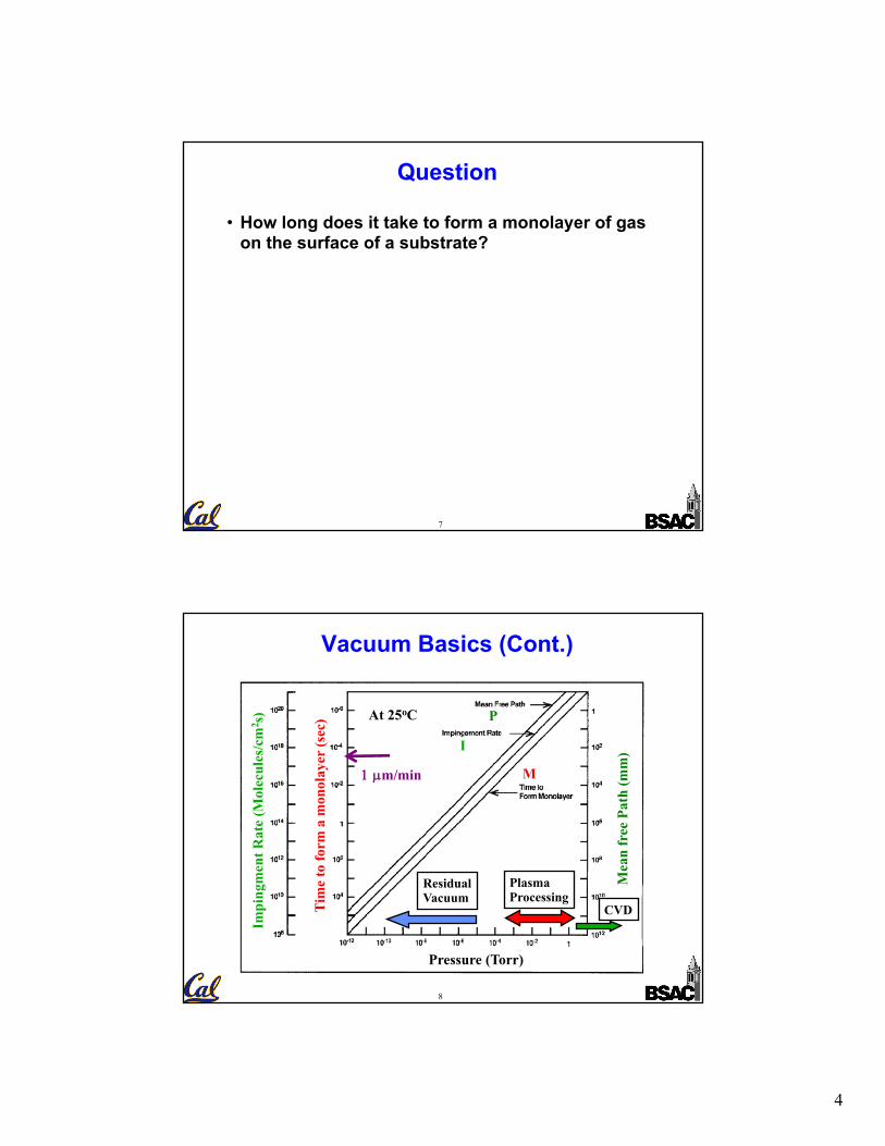
7
Question
• How long does it take to form a monolayer of gas on the surface of a substrate?
8
Pressure (Torr)
Tim
e to
form
a m
onol
ayer
(sec
)
Impi
ngm
entR
ate
(Mol
ecul
es/c
m2 s
)
Mea
n fr
ee P
ath
(mm
)
At 25oC
M
I
P
1 µm/min
ResidualVacuum
Plasma Processing
CVD
Vacuum Basics (Cont.)

5
9
Thin Film Deposition
• Applications– Metalization (e.g., Al, TiN, W, Silicide)– Polysilicon– Dielectric layers (SiO2, Si3N4)
substrateFilm
EvaporationSputtering Chemical Vapor Deposition (CVD)
Atomic Layer Deposition (ALD)
Physical Methods Chemical Methods
10
Evaporation
wafer
depositedAl film
Al vapor
Al
hot heatingboat (e.g. W)
electronsource
crucible is water cooled
Al vapor
e
wafer
depositedAl film
Thermal Evaporation Electron Beam Evaporation
Gas Pressure: < 10-5 Torr

6
11
Evaporation: Filament & Electron Beam
(a) Filament evaporation with loops of wire hanging from a heated filament
(b) Electron beam is focused on metal charge by a magnetic field
12
Al
Sputtering
• Gas pressure ~ 1 to 10 mTorr
• Deposition rate = constant × 𝑰 × 𝑺– Where 𝑰 = ion current– 𝑺 = sputtering yield
wafer
Al AlAr+
Deposited Al film
Al target
Ar plasma
heat substrate to ~ 300oC (optional)
Negative Bias ( kV)I
Ar+

7
13
Plasma Basics
14
Basic Properties of Plasma
• The bulk of plasma contains equal concentrations of ions and electrons.
• Electric potential is » constant inside bulk of plasma. The voltage drop is mostly across the sheath regions
• Plasma used in IC processing is a “weak” plasma, containing mostly neutral atoms/molecules. – Degree of ionization is » 10-3 to 10-6

8
15
Outcomes of Plasma bombardment
16
S º# of ejected target atoms
incoming ion.S º
# of ejected target atoms
incoming ion.
# of ejected target atoms
incoming ion.
0.1 < S < 30
Al
Al
Al
Ar AlAl
AlAl
Al
Ar
Sputtering Yield S
Sputtering Yield

9
17
Ar+
Aflux
Bflux
AxBy
Target
Because SA ¹ SB, target surface will acquire a composition Ax’By’ at steady state.
Sputtering of Compound Targets
18
Reactive Sputtering
Sputtering deposition while introducing a reactive gas into the plasma.
Example:
• Formation of TiN– Sputter a Ti target with a nitrogen plasma
Ti Target
N2 plasma
Ti, N2+
TiN
Substrate

10
19
Step Coverage Problem with PVD
• Both evaporation and sputtering have directional fluxes
wafer
step
filmFlux
film
“geometricalshadowing”
20
Step Coverage concerns in contacts

11
21
Sputtering Target
Methods to Minimize Step Coverage Problems
• Rotate + Tilt substrate during deposition
• Elevate substrate temperature (why?)
• Use large-area deposition source
22
Advantages of Sputtering over Evaporation
• For multi-component thin films, sputtering gives better composition control using compound targets. – Evaporation depends on vapor pressure of various vapor components and is difficult to control.
• Better lateral thickness uniformity– Superposition of multiple point sources
Sputtering Target
Profile due to one small-area source
Superposition of all small-area sources
Sputtering Target
Profile due to one small-area source
Superposition of all small-area sources

12
23
Chemical Vapor Deposition (CVD)
filmsubstrate
chemical reaction
source
More conformal deposition than PVD
step
t
tShown hereis 100% conformaldeposition
24
LPCVD Examples
• SiO2𝑺𝒊𝑯𝟒 + 𝑶𝟐
𝟑𝟓𝟎~𝟓𝟎𝟎℃𝑺𝒊𝑶𝟐 + 𝟐𝑯𝟐 ↑
• PSG (phosphosilicate glass): doped glass– (~ 𝟓% 𝑷𝟐𝑶𝟓 + 𝟗𝟓% 𝑺𝒊𝑶𝟐)– The film “reflows” at 900℃
𝟒𝑷𝑯𝟑 + 𝟓𝑶𝟐𝟑𝟓𝟎~𝟓𝟎𝟎℃
𝟐𝑷𝟐𝑶𝟓 + 𝟔𝑯𝟐 ↑𝑺𝒊𝑯𝟒 + 𝑶𝟐
𝟑𝟓𝟎~𝟓𝟎𝟎℃𝑺𝒊𝑶𝟐 + 𝟐𝑯𝟐 ↑

13
25
LPCVD Examples
• TEOS (Tetraethylorthosilicate) Si(OC2H5)4
𝑺𝒊(𝑶𝑪𝟐𝑯𝟓)𝟒→ 𝑺𝒊𝑶𝟐 + 𝑪𝑿𝑯𝒀𝑶𝒁 ↑
– The liquid chemical TEOS is a safer alternative to gases silane or dichlorosilane
Molecular structure of TEOS
26
LPCVD Examples
• Si3N4𝟑𝑺𝒊𝑯𝟒 + 𝟒𝑵𝑯𝟑 → 𝑺𝒊𝟑𝑵𝟒 + 𝟏𝟐𝑯𝟐 ↑
• Polysilicon
𝑺𝒊𝑯𝟒VWW°Y
𝑺𝒊 + 𝟐𝑯𝟐 ↑
• Tungsten 𝑾𝑭𝟔 + 𝟑𝑯𝟐 → 𝑾+ 𝟔𝑯𝑭 ↑

14
27
CVD Mechanisms
reactant
1
2
5
43
stagnantgas layer
surfacediffusion
1 = Diffusion of reactant to surface2 = Absorption of reactant to surface3 = Chemical reaction4 = Desorption of gas by-products5 = Out-diffusion of by-product gas
Substrate
28
CVD Deposition Rate [Grove Model]
F1 F3
film
d = thickness of stagnant layerd
Si
𝑭𝟏 = 𝑫𝑪𝑮 − 𝑪𝑺
𝜹𝑭𝟑 = 𝒌𝑺𝑪𝑺
At steady state, 𝑭𝟏 = 𝑭𝟑
𝑫𝜹 = 𝒉𝑮
𝒌𝑺 = 𝒌𝟎𝒆b𝚫𝑬𝒌𝑻

15
29
Grove model of CVD (cont’d)
𝑭𝟏 = 𝑫𝑪𝑮 − 𝑪𝑺
𝜹 = 𝒉𝑮 𝑪𝑮 − 𝑪𝑺 = 𝒌𝑺𝑪𝑺 = 𝑭𝟑
𝑪𝑺 = 𝒉𝑮
𝒌𝑺 + 𝒉𝑮𝑪𝑮
𝑭𝟑 = 𝒌𝑺𝒉𝑮𝒌𝑺 + 𝒉𝑮
𝑪𝑮 = 𝟏
𝟏𝒉𝑮
+ 𝟏𝒌𝑺
𝑪𝑮
Film growth rate is constant with time:𝒅𝒙𝒅𝒕 =
𝑭𝟑𝑵
where 𝑵 = atomic density of deposited film
Note: This result is exactly the same as the Deal-Grove modelfor thermal oxidation with oxide thickness = 0
30
Deposition Rate vs. Temperature
Deposition Rate
[log scale]
0
gas transport limited
surface-reactionlimited
1 / T
low Thigh T
𝑹 ∝ 𝑻 𝟑𝟐

16
31
Growth Rate Dependence on Flow Velocity
32
CVD Features
1. More conformal deposition if T is uniform
2. Inter-wafer and intra-wafer thickness uniformity less sensitive to gas flow patterns. (i.e. wafer placement).
Wafer topography

17
33
Comments about CVD
(2) Mass depletion problem
inout
more less
(1) Sensitivity to gas flow patternFurnace tube
wafersin
34
Plasma Enhanced CVD (PECVD)• Ionized chemical species allows a lower process temperature to be used – Plasma helps dissociate the precursor molecules at lower temperatures).
• Film properties (e.g. mechanical stress) can be tailored by controlling ion bombardment with substrate bias voltage.

18
35
Atomic Layer Deposition (ALD)
• The process involves two self-limiting half reactions that are repeated in cycles
• Unlike CVD, in ALD pulses of precursors are introduced in each cycle
• ALD is highly conformal and enables excellent thickness uniformity and control down to nm-scale
36
ALD for High-k Gate Dielectric