Embed Size (px)
Citation preview
Thin film analysis
Advanced X-ray Workshop, S.N. Bose National Centre
Innovation with Integrity
14-15/12/2011 2
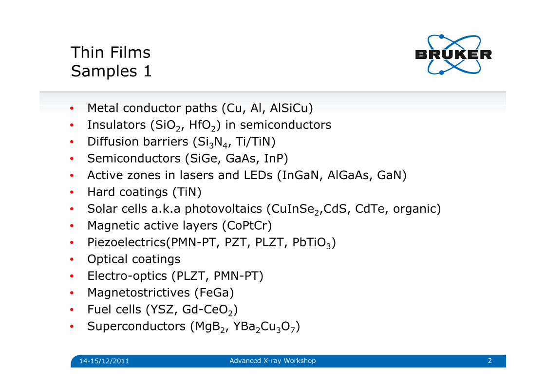
• Metal conductor paths (Cu, Al, AlSiCu)• Insulators (SiO2, HfO2) in semiconductors• Diffusion barriers (Si3N4, Ti/TiN)• Semiconductors (SiGe, GaAs, InP)• Active zones in lasers and LEDs (InGaN, AlGaAs, GaN)• Hard coatings (TiN) • Solar cells a.k.a photovoltaics (CuInSe2,CdS, CdTe, organic)• Magnetic active layers (CoPtCr)• Piezoelectrics(PMN-PT, PZT, PLZT, PbTiO3) • Optical coatings• Electro-optics (PLZT, PMN-PT)• Magnetostrictives (FeGa)• Fuel cells (YSZ, Gd-CeO2)• Superconductors (MgB2, YBa2Cu3O7)
Thin FilmsSamples 1
Advanced X-ray Workshop
14-15/12/2011 3
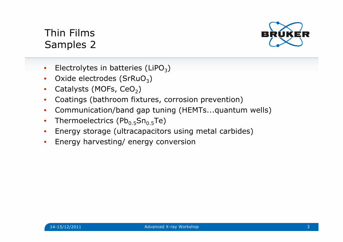
• Electrolytes in batteries (LiPO3) • Oxide electrodes (SrRuO3)• Catalysts (MOFs, CeO2) • Coatings (bathroom fixtures, corrosion prevention)• Communication/band gap tuning (HEMTs...quantum wells)• Thermoelectrics (Pb0.5Sn0.5Te) • Energy storage (ultracapacitors using metal carbides)• Energy harvesting/ energy conversion
Thin FilmsSamples 2
Advanced X-ray Workshop
14-15/12/2011 4
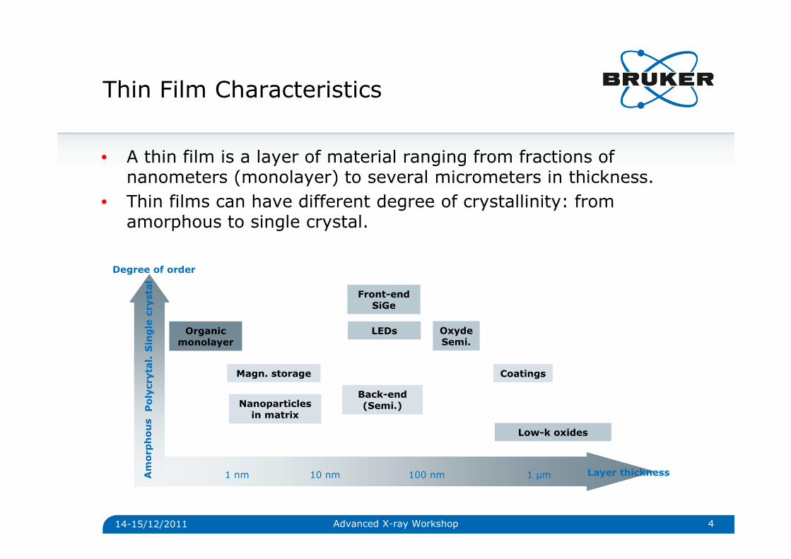
• A thin film is a layer of material ranging from fractions of nanometers (monolayer) to several micrometers in thickness.
• Thin films can have different degree of crystallinity: from amorphous to single crystal.
Thin Film Characteristics
Organic monolayer
Nanoparticlesin matrix
Back-end (Semi.)
Front-endSiGe
OxydeSemi.
1 µm100 nm10 nm1 nm Layer thickness
Low-k oxides
Degree of order
AmorphousPolycrytal.Single crystal
CoatingsMagn. storage
LEDs
Advanced X-ray Workshop
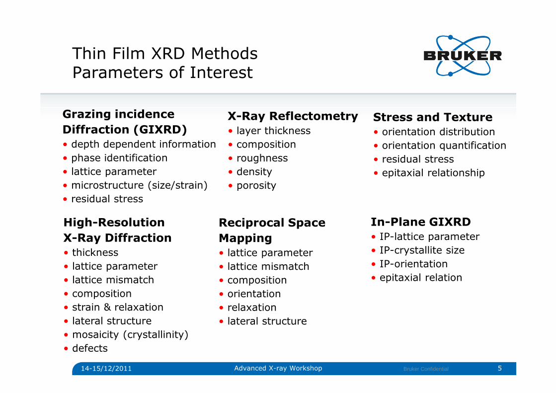
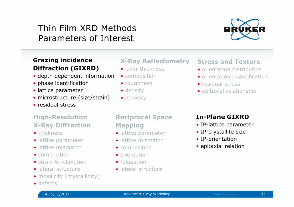
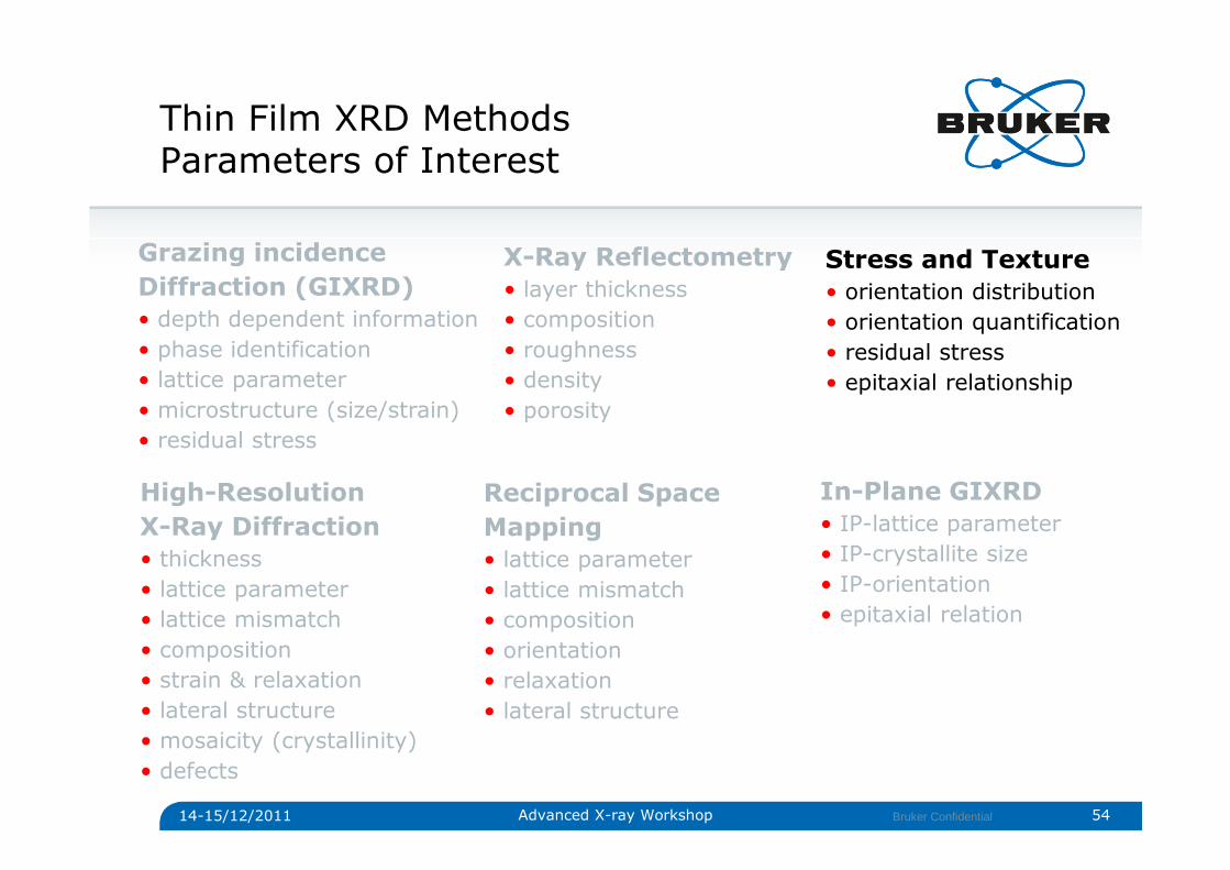
Thin Film XRD MethodsParameters of Interest
14-15/12/2011 5Bruker Confidential
High-Resolution
X-Ray Diffraction
• thickness• lattice parameter• lattice mismatch• composition• strain & relaxation• lateral structure• mosaicity (crystallinity)• defects
X-Ray Reflectometry
• layer thickness• composition• roughness• density• porosity
Reciprocal Space
Mapping
• lattice parameter• lattice mismatch• composition• orientation• relaxation• lateral structure
Stress and Texture
• orientation distribution• orientation quantification• residual stress• epitaxial relationship
Grazing incidence
Diffraction (GIXRD)
• depth dependent information• phase identification• lattice parameter• microstructure (size/strain)• residual stress
In-Plane GIXRD
• IP-lattice parameter• IP-crystallite size• IP-orientation• epitaxial relation
Advanced X-ray Workshop

Thin Film XRD MethodsParameters of Interest
14-15/12/2011 6Bruker Confidential
High-Resolution
X-Ray Diffraction
• thickness• lattice parameter• lattice mismatch• composition• strain & relaxation• lateral structure• mosaicity (crystallinity)• defects
X-Ray Reflectometry
• layer thickness• composition• roughness• density• porosity
Reciprocal Space
Mapping
• lattice parameter• lattice mismatch• composition• orientation• relaxation• lateral structure
Stress and Texture
• orientation distribution• orientation quantification• residual stress• epitaxial relationship
Grazing incidence
Diffraction (GIXRD)
• depth dependent information• phase identification• lattice parameter• microstructure (size/strain)• residual stress
In-Plane GIXRD
• IP-lattice parameter• IP-crystallite size• IP-orientation• epitaxial relation
Advanced X-ray Workshop
7
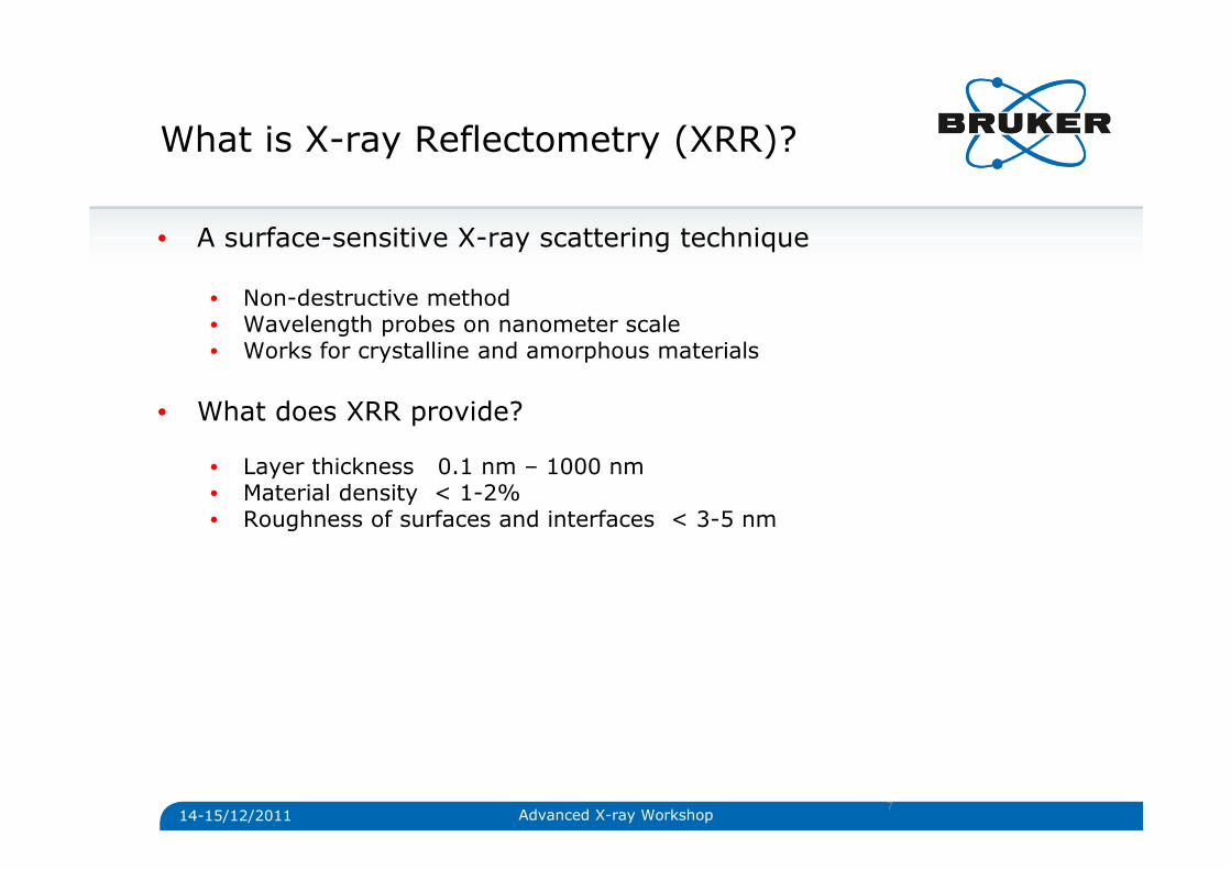
• A surface-sensitive X-ray scattering technique
• Non-destructive method• Wavelength probes on nanometer scale• Works for crystalline and amorphous materials
• What does XRR provide?
• Layer thickness 0.1 nm – 1000 nm• Material density < 1-2%• Roughness of surfaces and interfaces < 3-5 nm
What is X-ray Reflectometry (XRR)?
14-15/12/2011 Advanced X-ray Workshop

Analytical tasks
Lateral structure
Layer thickness ChemicalComposition
(electron density)
Roughness
Specular XRR Diffuse
14-15/12/2011 Advanced X-ray Workshop 8
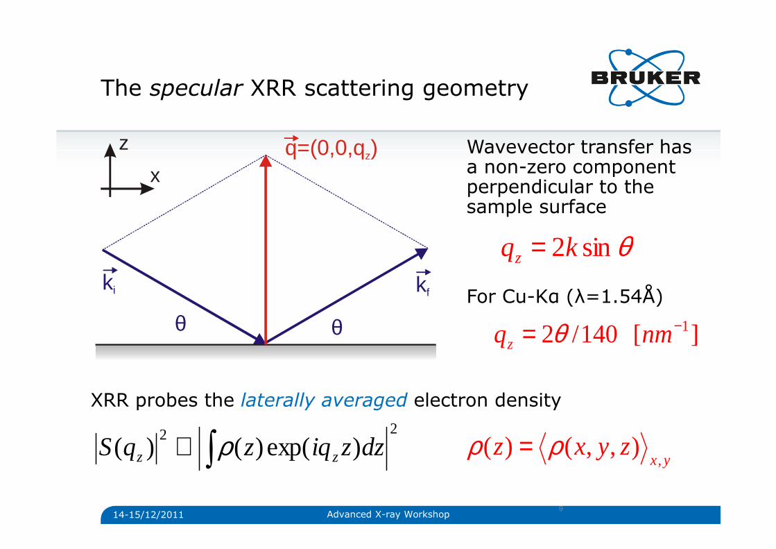
The specular XRR scattering geometry
9
Wavevector transfer has a non-zero component perpendicular to the sample surface
For Cu-Kα (λ=1.54Å)
XRR probes the laterally averaged electron density
yxzyxz
,),,()( ρρ =
q=(0,0,q )z
ki kf
θ θ
z
x
θsin2kqz =
22)exp()()( ∫∝ dzziqzqS zz ρ
][140/2 1−= nmqz θ
14-15/12/2011 Advanced X-ray Workshop
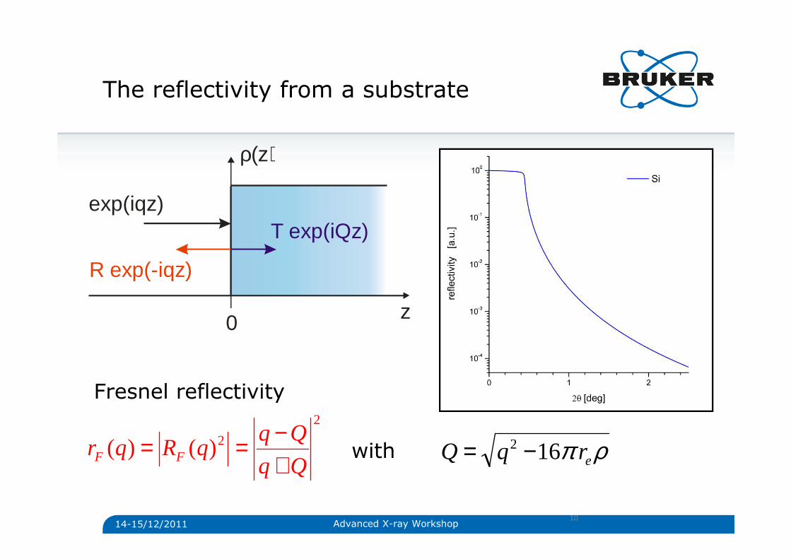
The reflectivity from a substrate
10
0 z
ρ( )z
exp(iqz)
R exp(-iqz)
T exp(iQz)
ρπ erqQ 162 −=2
2)()(Qq
QqqRqr FF +
−==
Fresnel reflectivity
with
14-15/12/2011 Advanced X-ray Workshop
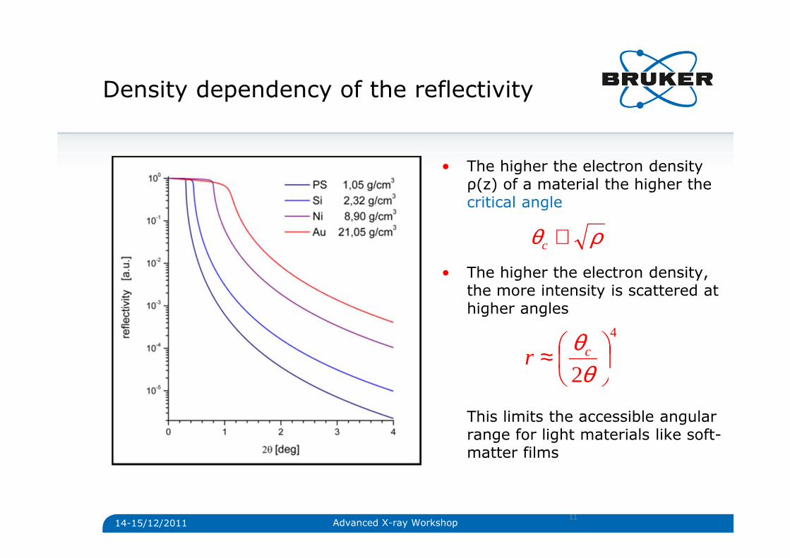
• The higher the electron density ρ(z) of a material the higher the critical angle
• The higher the electron density, the more intensity is scattered at higher angles
This limits the accessible angular range for light materials like soft-matter films
Density dependency of the reflectivity
11
ρθ ∝c
4
2
≈θ
θcr
14-15/12/2011 Advanced X-ray Workshop
12
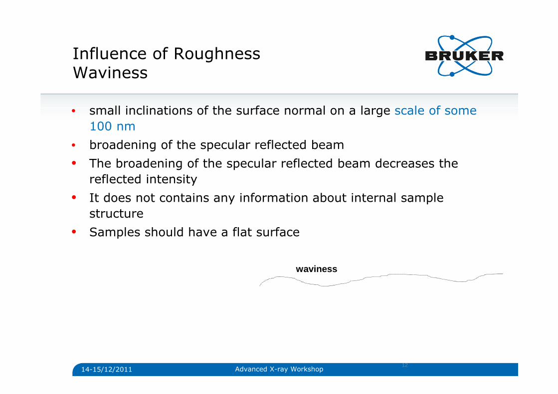
• small inclinations of the surface normal on a large scale of some 100 nm
• broadening of the specular reflected beam
• The broadening of the specular reflected beam decreases thereflected intensity
• It does not contains any information about internal sample structure
• Samples should have a flat surface
Influence of RoughnessWaviness
waviness
14-15/12/2011 Advanced X-ray Workshop

13
• large inclinations of the surface normal on an atomic scale of a few nanometers
• leads to diffuse reflection of the incident beam • the intensity of the specular reflected beam decreases
Influence of RoughnessMicroscopic Roughness
waviness
microscopicroughness
14-15/12/2011 Advanced X-ray Workshop
Influence of Roughness
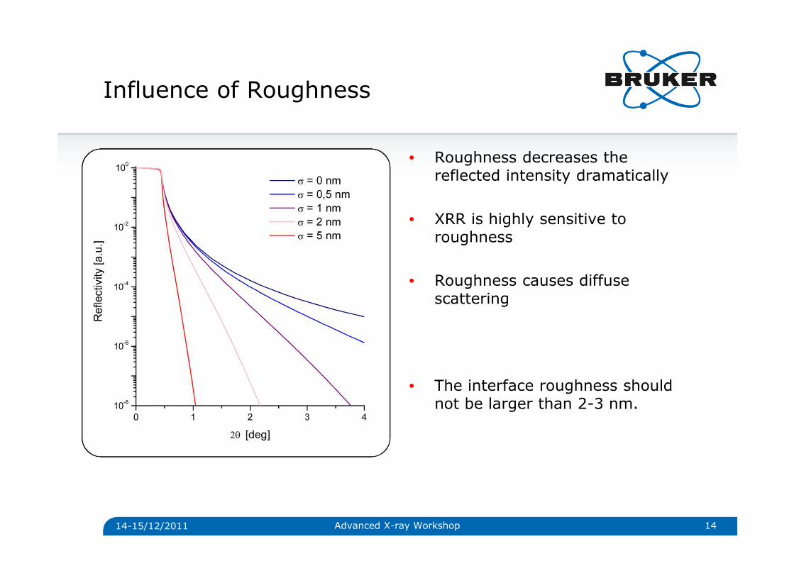
• Roughness decreases the reflected intensity dramatically
• XRR is highly sensitive to roughness
• Roughness causes diffuse scattering
• The interface roughness should not be larger than 2-3 nm.
14-15/12/2011 Advanced X-ray Workshop 14

XRR from single layer on substrate: Thickness fringes
15
• The interference of the waves reflected from the interfaces causes oscillations of period
• The minimal observable thickness is limited by the maximal measurable range
• The maximal observable thickness is limited by the instrumental resolution
• The sample should have thicknesses observable with the instrumental setup.
dqz /2π=∆
14-15/12/2011 Advanced X-ray Workshop
Thickness fringesAmplitude
16
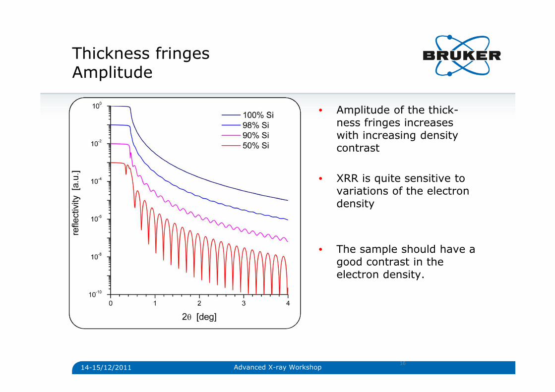
• Amplitude of the thick-ness fringes increases with increasing density contrast
• XRR is quite sensitive to variations of the electron density
• The sample should have a good contrast in the electron density.
14-15/12/2011 Advanced X-ray Workshop
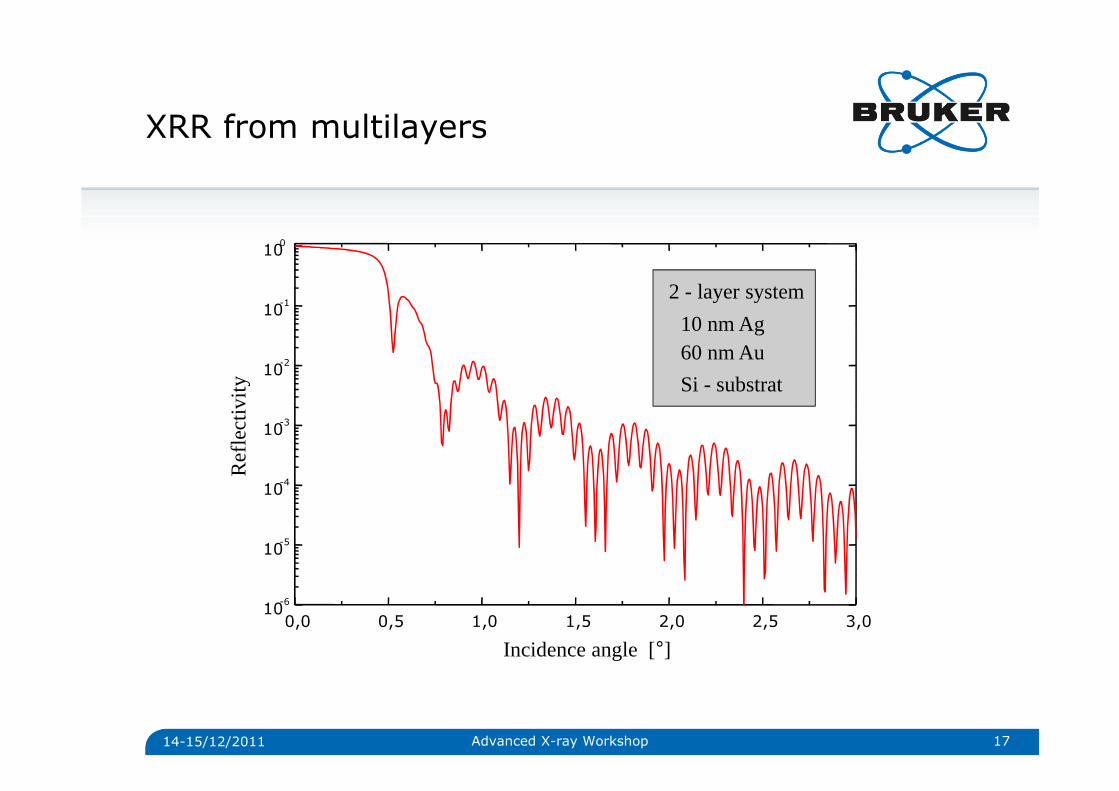
XRR from multilayers
0,0 0,5 1,0 1,5 2,0 2,5 3,010-6
10-5
10-4
10-3
10-2
10-1
100
2 - layer system
10 nm Ag60 nm Au
Si - substrat
Ref
lect
ivity
Incidence angle [°]
14-15/12/2011 Advanced X-ray Workshop 17
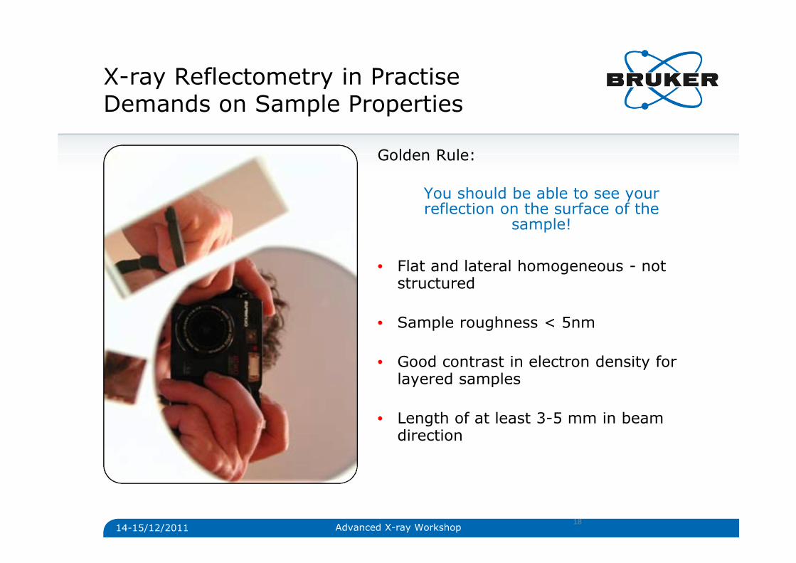
X-ray Reflectometry in PractiseDemands on Sample Properties
18
Golden Rule:
You should be able to see your reflection on the surface of the
sample!
• Flat and lateral homogeneous - not structured
• Sample roughness < 5nm
• Good contrast in electron density for layered samples
• Length of at least 3-5 mm in beam direction
14-15/12/2011 Advanced X-ray Workshop

19
• Reasonable resolution requires slit of 50-100 µm • Intensity is on the order of 107 cps• Full energy spectrum creates high background
Simplest Setup for XRR
14-15/12/2011 Advanced X-ray Workshop
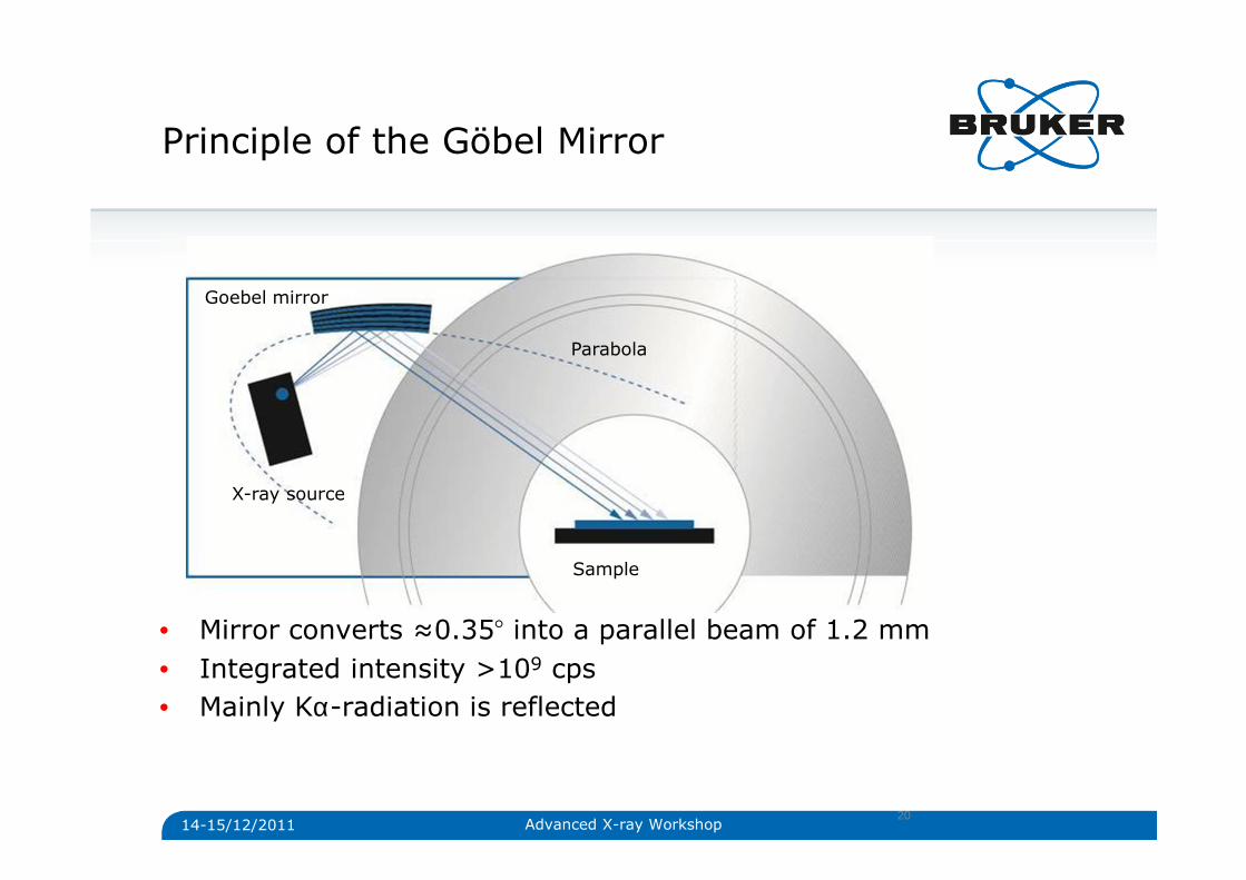
20
• Mirror converts ≈0.35° into a parallel beam of 1.2 mm• Integrated intensity >109 cps• Mainly Kα-radiation is reflected
Principle of the Göbel Mirror
Parabola
X-ray source
Goebel mirror
Sample
14-15/12/2011 Advanced X-ray Workshop
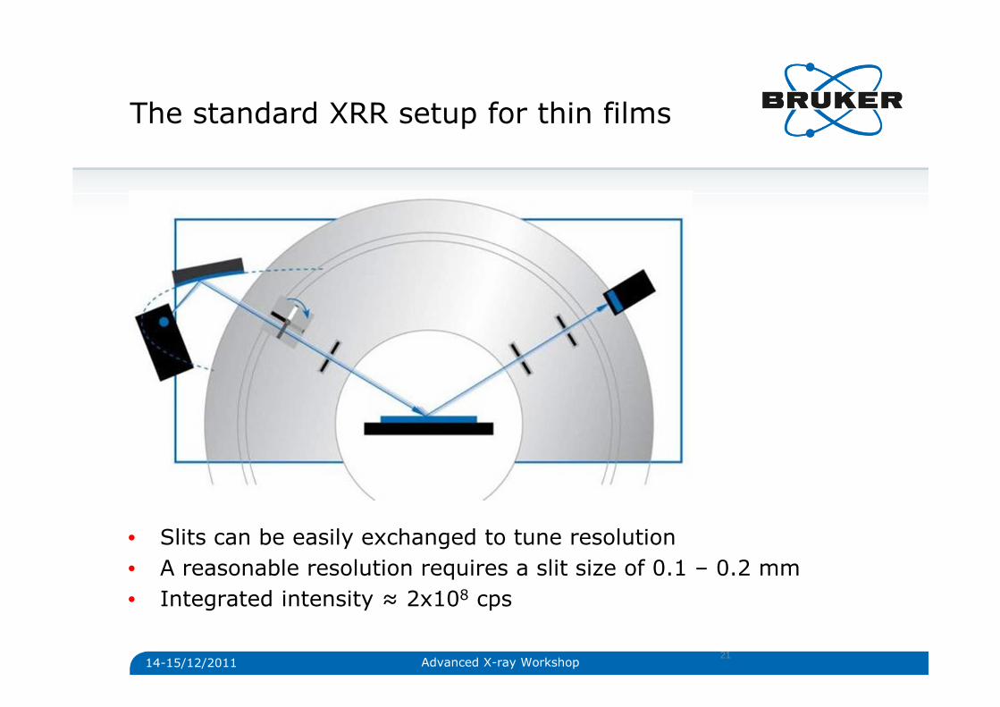
21
• Slits can be easily exchanged to tune resolution• A reasonable resolution requires a slit size of 0.1 – 0.2 mm • Integrated intensity ≈ 2x10⁸ cps
The standard XRR setup for thin films
14-15/12/2011 Advanced X-ray Workshop
22
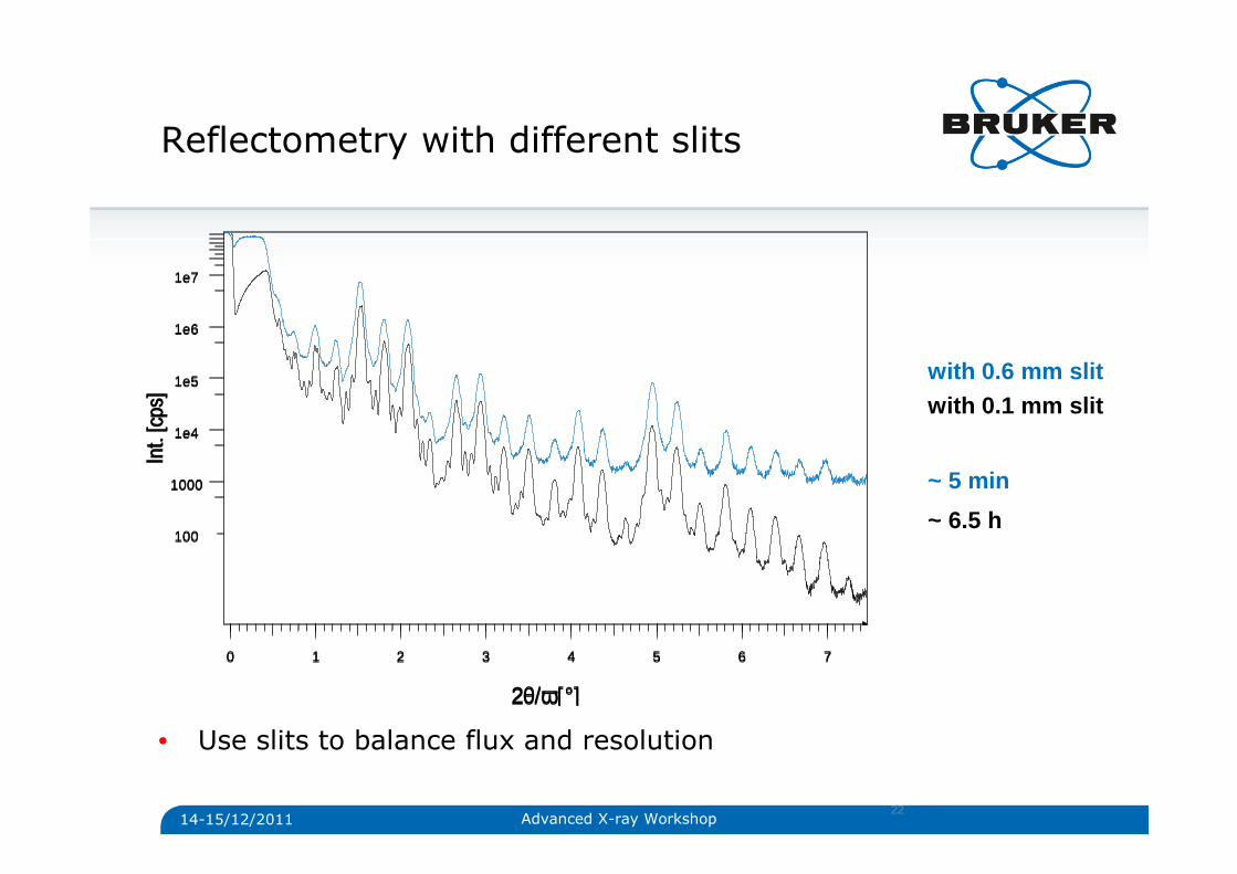
• Use slits to balance flux and resolution
Reflectometry with different slitsIn
t. [c
ps]
100
1000
1e4
1e5
1e6
1e7
2θ/ω[°]
0 1 2 3 4 5 6 7
with 0.6 mm slitwith 0.1 mm slit
~ 5 min
~ 6.5 h
Int.
[cps
]
100
1000
1e4
1e5
1e6
1e7
2θ/ω[°]
0 1 2 3 4 5 6 7
14-15/12/2011 Advanced X-ray Workshop
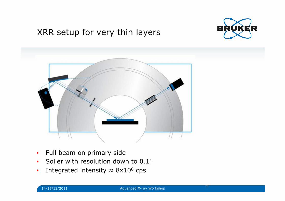
23
• Full beam on primary side• Soller with resolution down to 0.1°• Integrated intensity ≈ 8x10⁸ cps
XRR setup for very thin layers
14-15/12/2011 Advanced X-ray Workshop
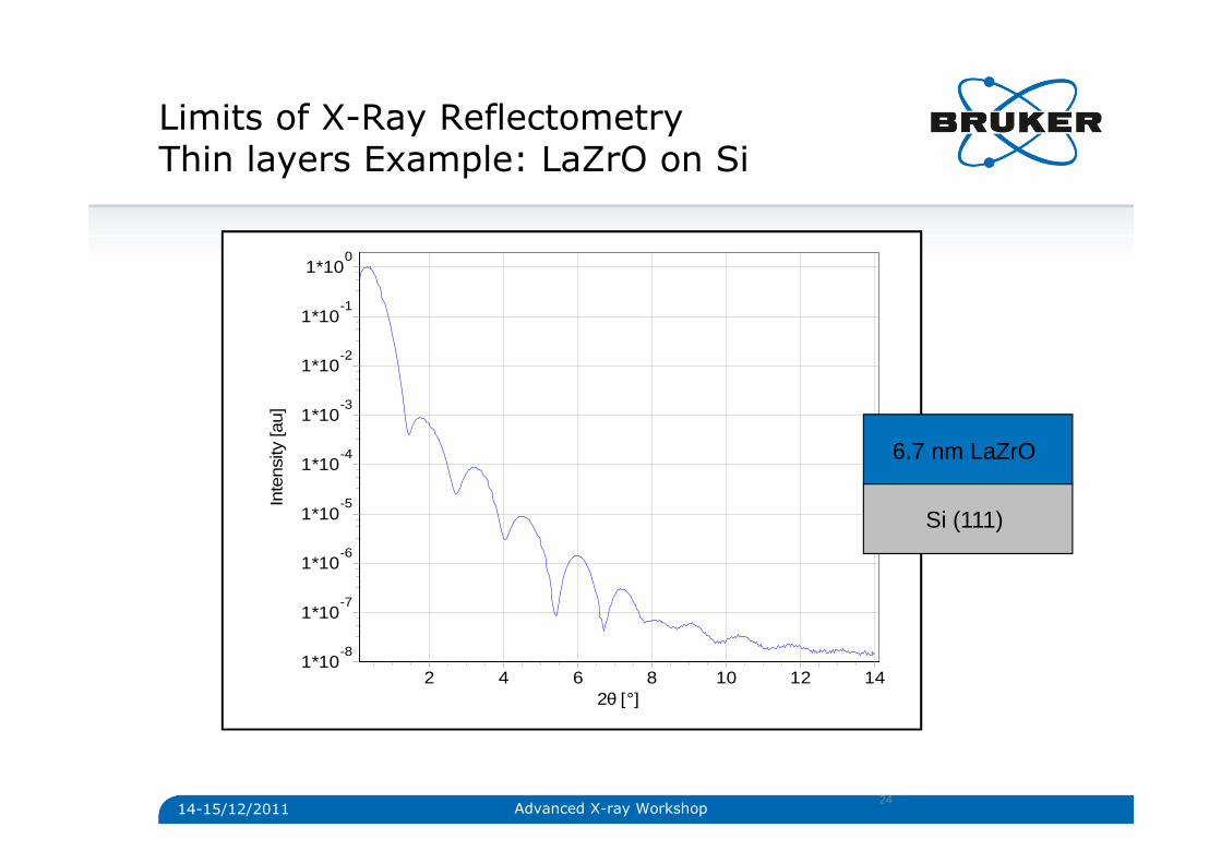
Limits of X-Ray Reflectometry Thin layers Example: LaZrO on Si
24
2θ [°]1412108642
Inte
nsity
[au]
-81*10
-71*10
-61*10
-51*10
-41*10
-31*10
-21*10
-11*10
01*10
Si (111)
6.7 nm LaZrO
14-15/12/2011 Advanced X-ray Workshop
25
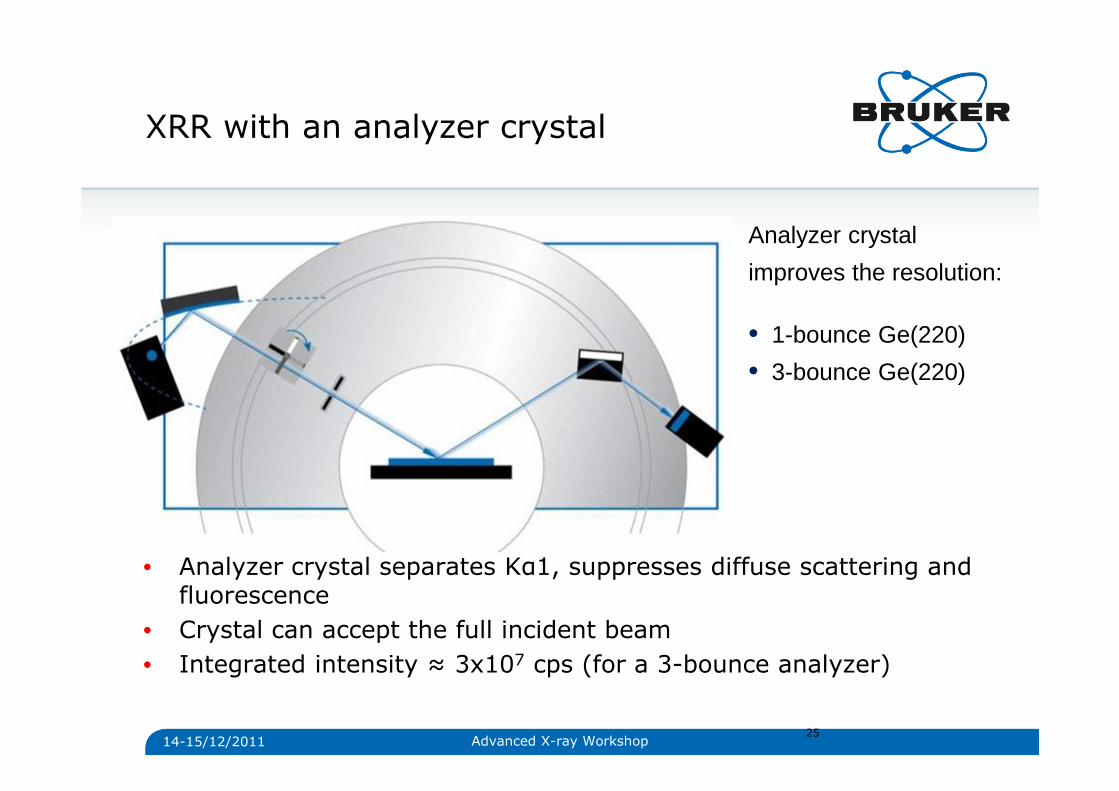
• Analyzer crystal separates Kα1, suppresses diffuse scattering and fluorescence
• Crystal can accept the full incident beam • Integrated intensity ≈ 3x10⁷ cps (for a 3-bounce analyzer)
XRR with an analyzer crystal
Analyzer crystal
improves the resolution:
• 1-bounce Ge(220)
• 3-bounce Ge(220)
14-15/12/2011 Advanced X-ray Workshop
26
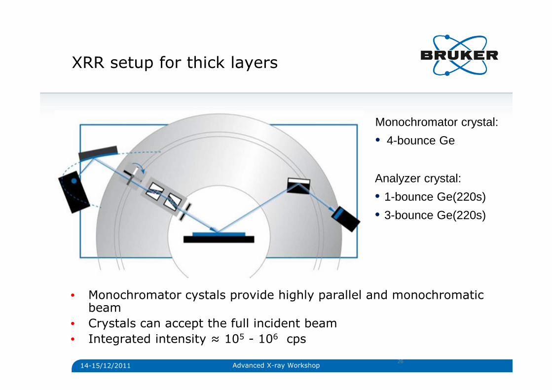
• Monochromator cystals provide highly parallel and monochromatic beam
• Crystals can accept the full incident beam • Integrated intensity ≈ 105 - 106 cps
XRR setup for thick layers
Analyzer crystal:
• 1-bounce Ge(220s)
• 3-bounce Ge(220s)
Monochromator crystal:
• 4-bounce Ge
14-15/12/2011 Advanced X-ray Workshop
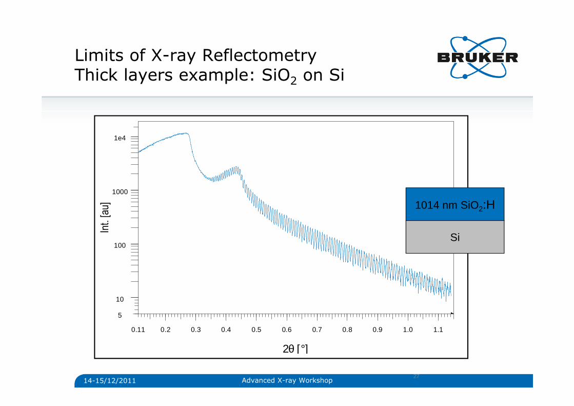
Limits of X-ray Reflectometry Thick layers example: SiO2 on Si
27
Int.
[au]
5
10
100
1000
1e4
2θ [°]
0.11 0.2 0.3 0.4 0.5 0.6 0.7 0.8 0.9 1.0 1.1
Si
1014 nm SiO2:H
14-15/12/2011 Advanced X-ray Workshop
28
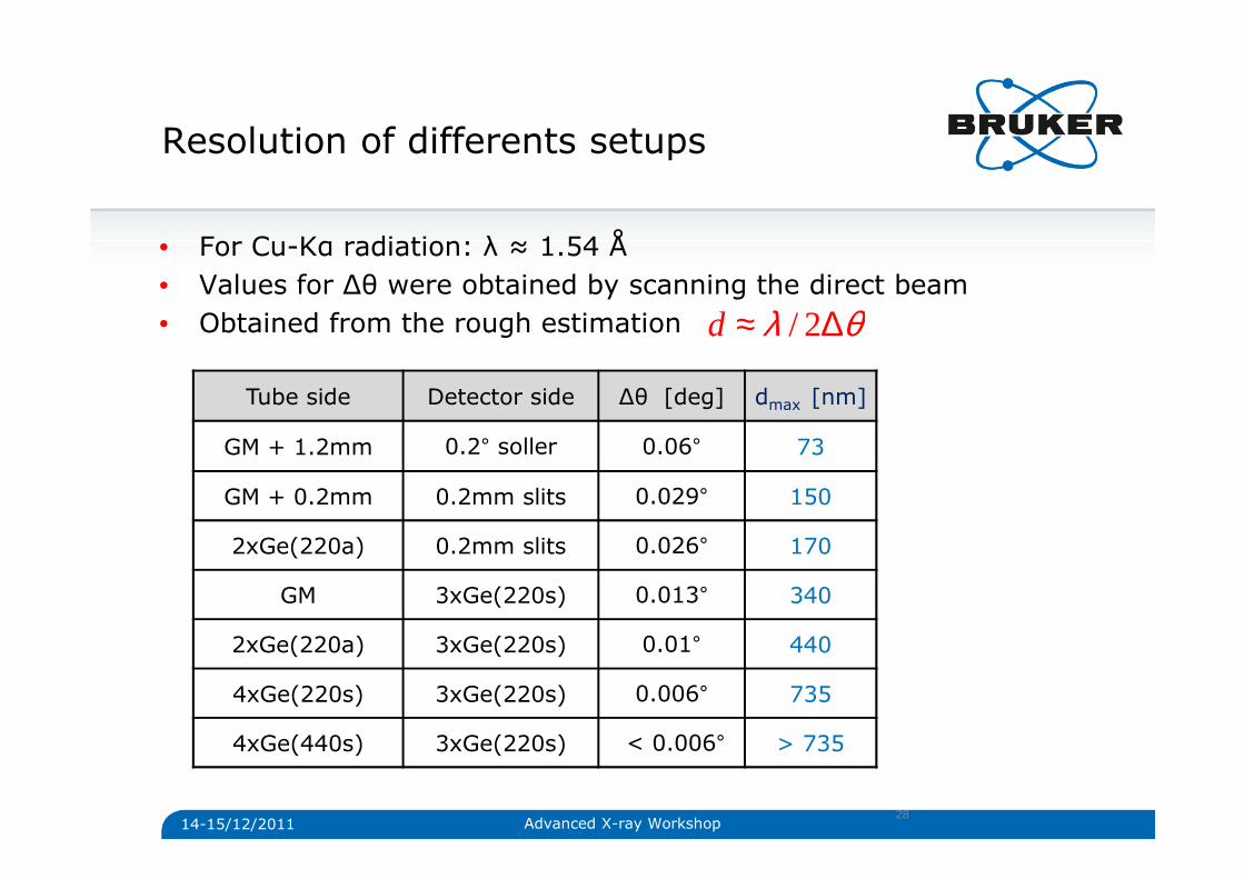
• For Cu-Kα radiation: λ ≈ 1.54 Å• Values for ∆θ were obtained by scanning the direct beam• Obtained from the rough estimation
Resolution of differents setups
θλ ∆≈ 2/d
Tube side Detector side ∆θ [deg] dmax [nm]
GM + 1.2mm 0.2° soller 0.06° 73
GM + 0.2mm 0.2mm slits 0.029° 150
2xGe(220a) 0.2mm slits 0.026° 170
GM 3xGe(220s) 0.013° 340
2xGe(220a) 3xGe(220s) 0.01° 440
4xGe(220s) 3xGe(220s) 0.006° 735
4xGe(440s) 3xGe(220s) < 0.006° > 735
14-15/12/2011 Advanced X-ray Workshop
29
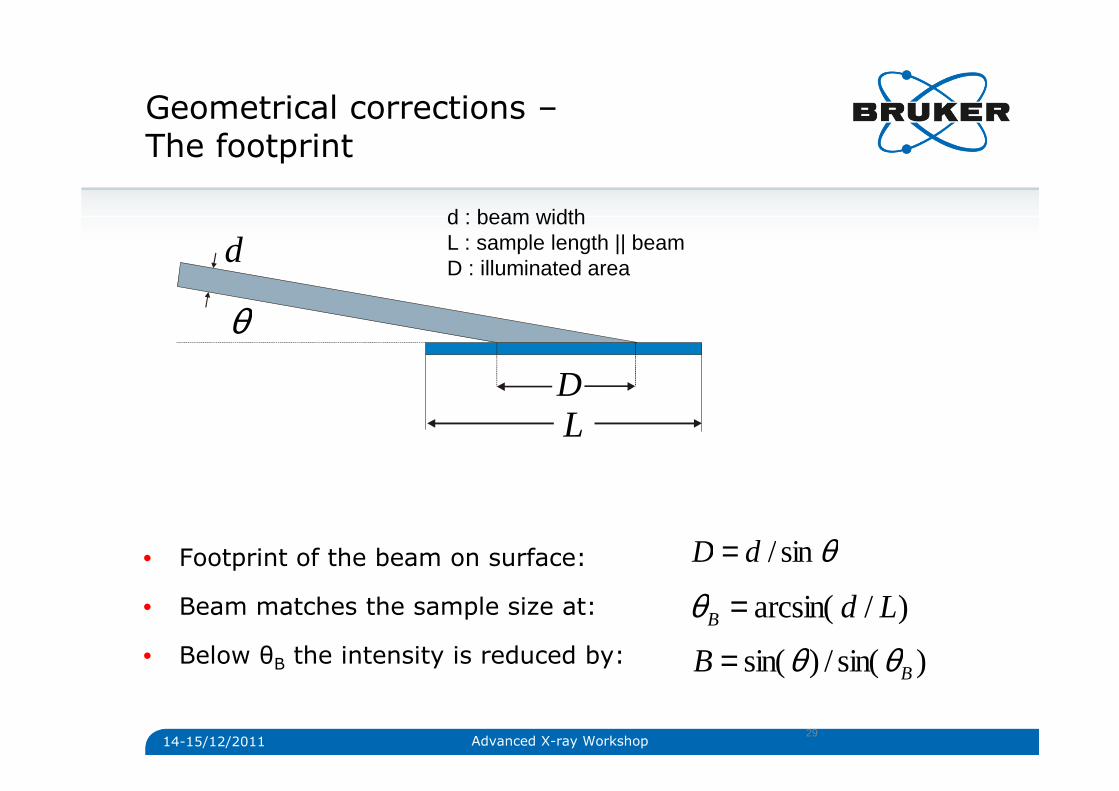
• Footprint of the beam on surface:
• Beam matches the sample size at:
• Below θB the intensity is reduced by:
Geometrical corrections –The footprint
)/arcsin( LdB =θ)sin(/)sin( BB θθ=
θsin/dD =
d : beam widthL : sample length || beamD : illuminated area
L
d
θ
D
14-15/12/2011 Advanced X-ray Workshop

30
• Sample size reduces the reflected intensity at small angles • Sample must be sufficiently large for XRR
Geometrical corrections –The footprint
Beamsize : 200 µm
14-15/12/2011 Advanced X-ray Workshop
31
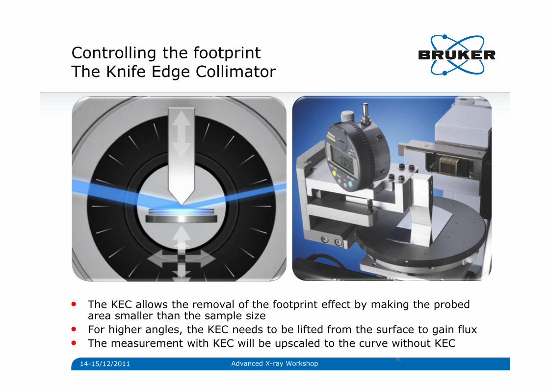
• The KEC allows the removal of the footprint effect by making the probedarea smaller than the sample size
• For higher angles, the KEC needs to be lifted from the surface to gain flux• The measurement with KEC will be upscaled to the curve without KEC
Controlling the footprintThe Knife Edge Collimator
14-15/12/2011 Advanced X-ray Workshop
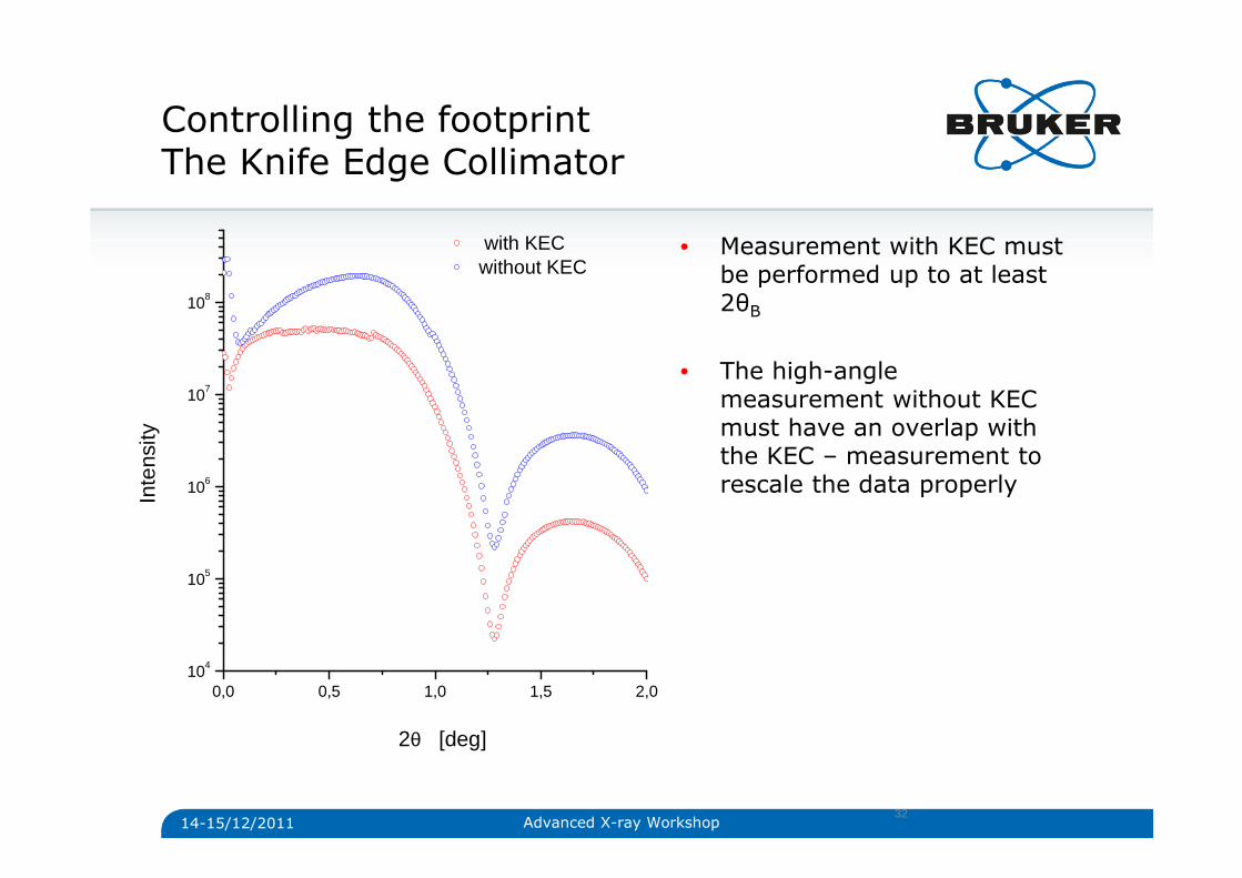
Controlling the footprintThe Knife Edge Collimator
32
• Measurement with KEC must be performed up to at least 2θB
• The high-angle measurement without KEC must have an overlap with the KEC – measurement to rescale the data properly
0,0 0,5 1,0 1,5 2,0104
105
106
107
108
with KECwithout KEC
Inte
nsity
2θ [deg]
14-15/12/2011 Advanced X-ray Workshop

Evaluation of SampleFitting Procedure
Sample Model parameterized by {p1,…pN}
Tolerance
XRR Simulation
Comparison with Experiment, χ2 cost function
Minimization of χ2 using Genetic Algorithm, Levenberg-Marquardt, Simplex,Simulated Annealing, etc. in view of {p1..pN}
14-15/12/2011 Advanced X-ray Workshop 33
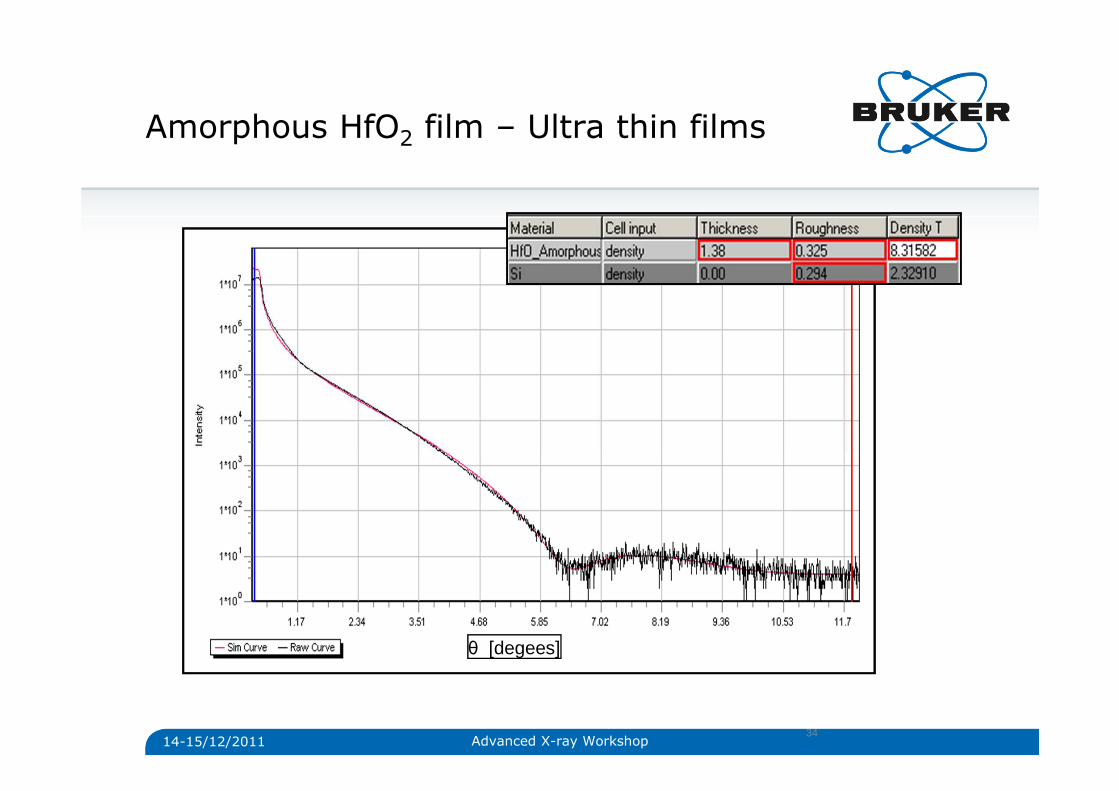
Amorphous HfO2 film – Ultra thin films
34
θ [degees]
14-15/12/2011 Advanced X-ray Workshop
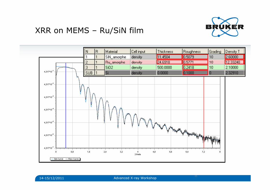
XRR on MEMS – Ru/SiN film
3514-15/12/2011 Advanced X-ray Workshop
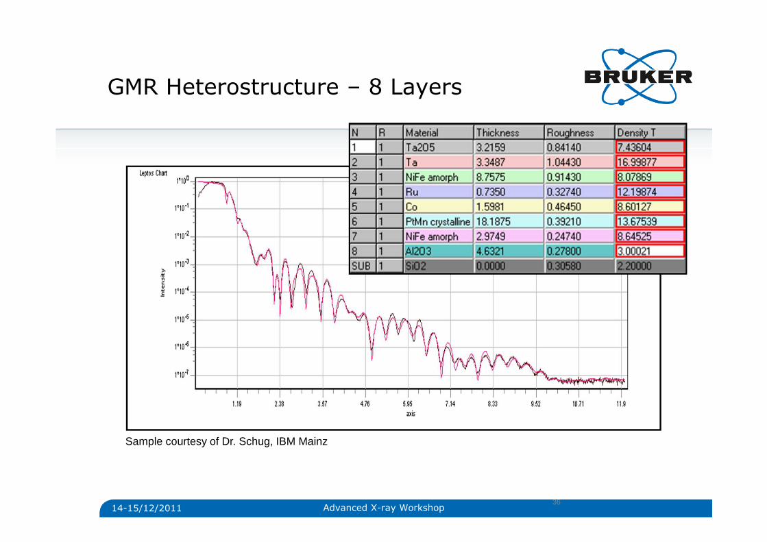
GMR Heterostructure – 8 Layers
36
Sample courtesy of Dr. Schug, IBM Mainz
14-15/12/2011 Advanced X-ray Workshop
Thin Film XRD MethodsParameters of Interest
14-15/12/2011 37Bruker Confidential
High-Resolution
X-Ray Diffraction
• thickness• lattice parameter• lattice mismatch• composition• strain & relaxation• lateral structure• mosaicity (crystallinity)• defects
X-Ray Reflectometry
• layer thickness• composition• roughness• density• porosity
Reciprocal Space
Mapping
• lattice parameter• lattice mismatch• composition• orientation• relaxation• lateral structure
Stress and Texture
• orientation distribution• orientation quantification• residual stress• epitaxial relationship
Grazing incidence
Diffraction (GIXRD)
• depth dependent information• phase identification• lattice parameter• microstructure (size/strain)• residual stress
In-Plane GIXRD
• IP-lattice parameter• IP-crystallite size• IP-orientation• epitaxial relation
Advanced X-ray Workshop
14-15/12/2011 38
• For coatings (few microns down to sub-micron range), the Bragg-Brentano geometry (BB) is still the best configuration. This is basically the classical powder diffraction case and BB will offer the best grain statistic and the easiest instrumental function characterization.
• Providing that the preferred orientation is weak, quantitative phase analysis or microstructure investigation (size/strain) are quite easy to perform.
• Limitations of the BB set-up: If the substrate is a single crystal, the huge intensity from the substrate peak will emphasize all minor peaks originating from the energy spectrum of the tube and other aberrations (Kβ, tube tails, Ni absorption edge, W lines,…) with the consequence that a significant part of the scan won’t be usable.
Remarks for Coatings
Advanced X-ray Workshop
14-15/12/2011 39
Even if a layer is polycrystalline, several characteristics differentiate a polycrystalline thin film with a loosed powder:
• Due to the limited layer thickness, the grain statistics is limited. The classical BB geometry might fail in providing necessary peak intensity for further analysis. An alternative is then to go for GIXRD.
• The confinement of the grains into a limited volume very often causes preferred orientation and the quantitative phase analysis might become impossible.
• The grain interaction during growth can also induce residual stress.
• A composition gradient through the layer may also appear during the growth.
Polycrystalline Thin FilmsConstrains
Advanced X-ray Workshop
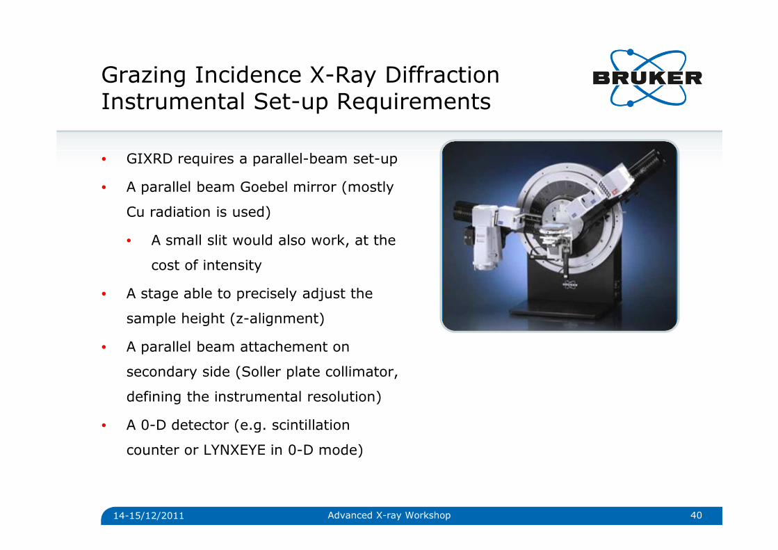
Grazing Incidence X-Ray DiffractionInstrumental Set-up Requirements
14-15/12/2011 40
• GIXRD requires a parallel-beam set-up
• A parallel beam Goebel mirror (mostly
Cu radiation is used)
• A small slit would also work, at the
cost of intensity
• A stage able to precisely adjust the
sample height (z-alignment)
• A parallel beam attachement on
secondary side (Soller plate collimator,
defining the instrumental resolution)
• A 0-D detector (e.g. scintillation
counter or LYNXEYE in 0-D mode)
Advanced X-ray Workshop
Lin
(Co
unts
)
0
1000
2000
3000
4000
5000
6000
7000
8000
9000
10000
11000
12000
13000
2-Theta - Scale
5 10 20 30 40 50 60 70 80 90
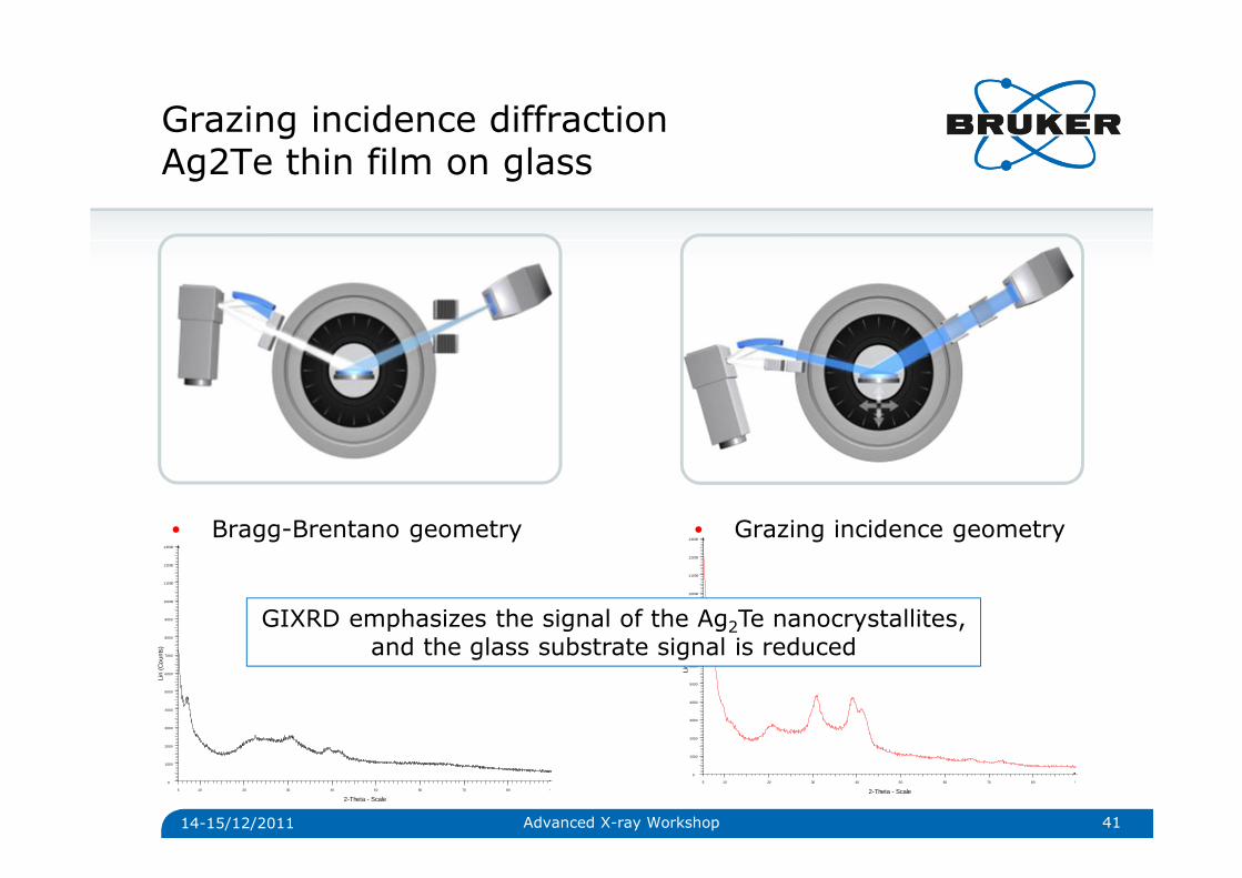
14-15/12/2011 41
• Bragg-Brentano geometry • Grazing incidence geometry
Lin
(Co
unts
)
0
1000
2000
3000
4000
5000
6000
7000
8000
9000
10000
11000
12000
13000
2-Theta - Scale
5 10 20 30 40 50 60 70 80 90
Grazing incidence diffractionAg2Te thin film on glass
GIXRD emphasizes the signal of the Ag2Te nanocrystallites,and the glass substrate signal is reduced
Advanced X-ray Workshop
14-15/12/2011 42
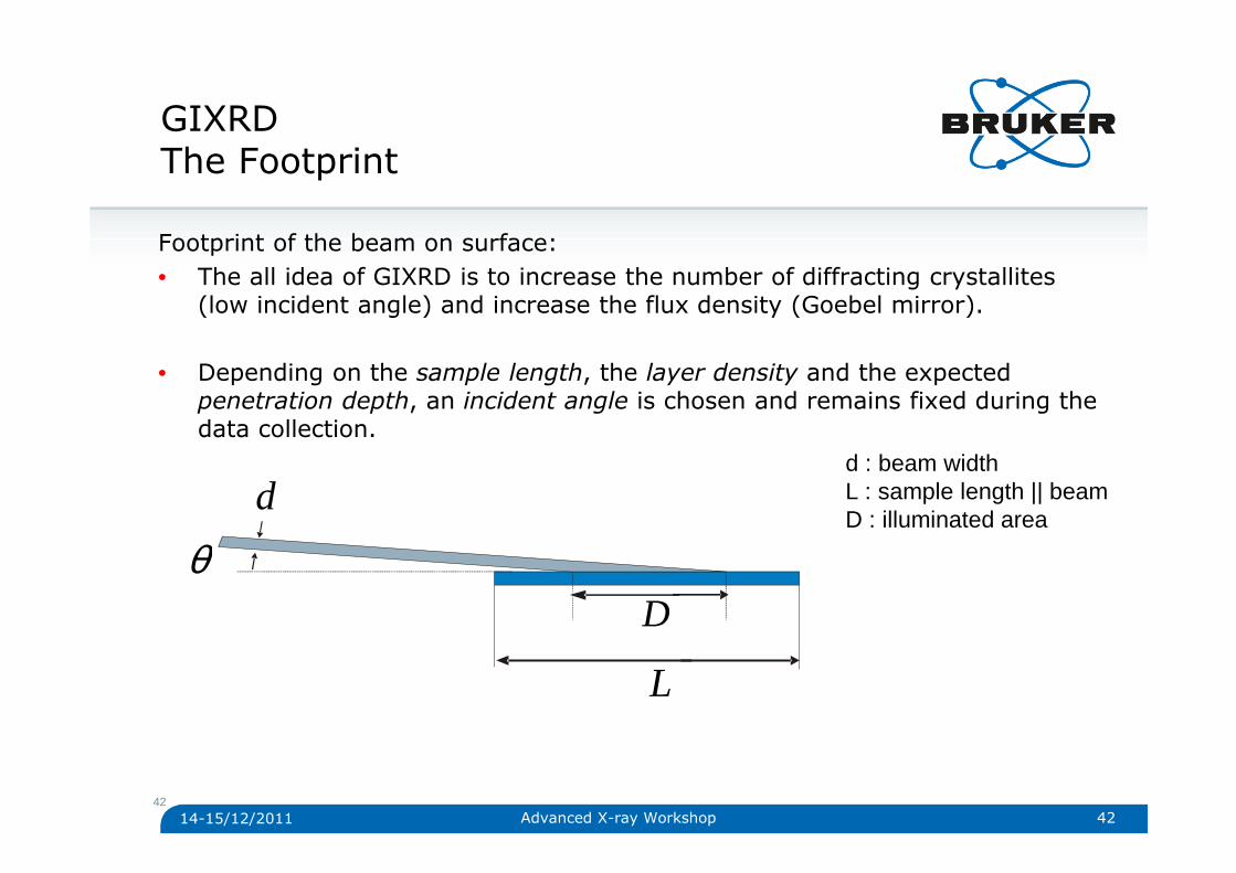
Footprint of the beam on surface:• The all idea of GIXRD is to increase the number of diffracting crystallites
(low incident angle) and increase the flux density (Goebel mirror).
• Depending on the sample length, the layer density and the expected penetration depth, an incident angle is chosen and remains fixed during the data collection.
GIXRDThe Footprint
42
d : beam widthL : sample length || beamD : illuminated area
L
d
θD
Advanced X-ray Workshop
14-15/12/2011 43
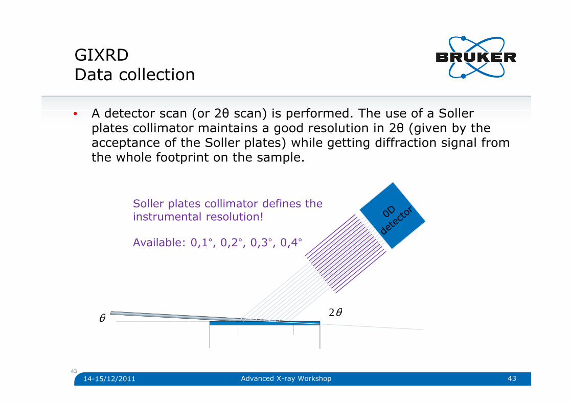
• A detector scan (or 2θ scan) is performed. The use of a Sollerplates collimator maintains a good resolution in 2θ (given by the acceptance of the Soller plates) while getting diffraction signal from the whole footprint on the sample.
GIXRDData collection
43
θ θ2
Soller plates collimator defines the instrumental resolution!
Available: 0,1°, 0,2°, 0,3°, 0,4°
Advanced X-ray Workshop
14-15/12/2011 44
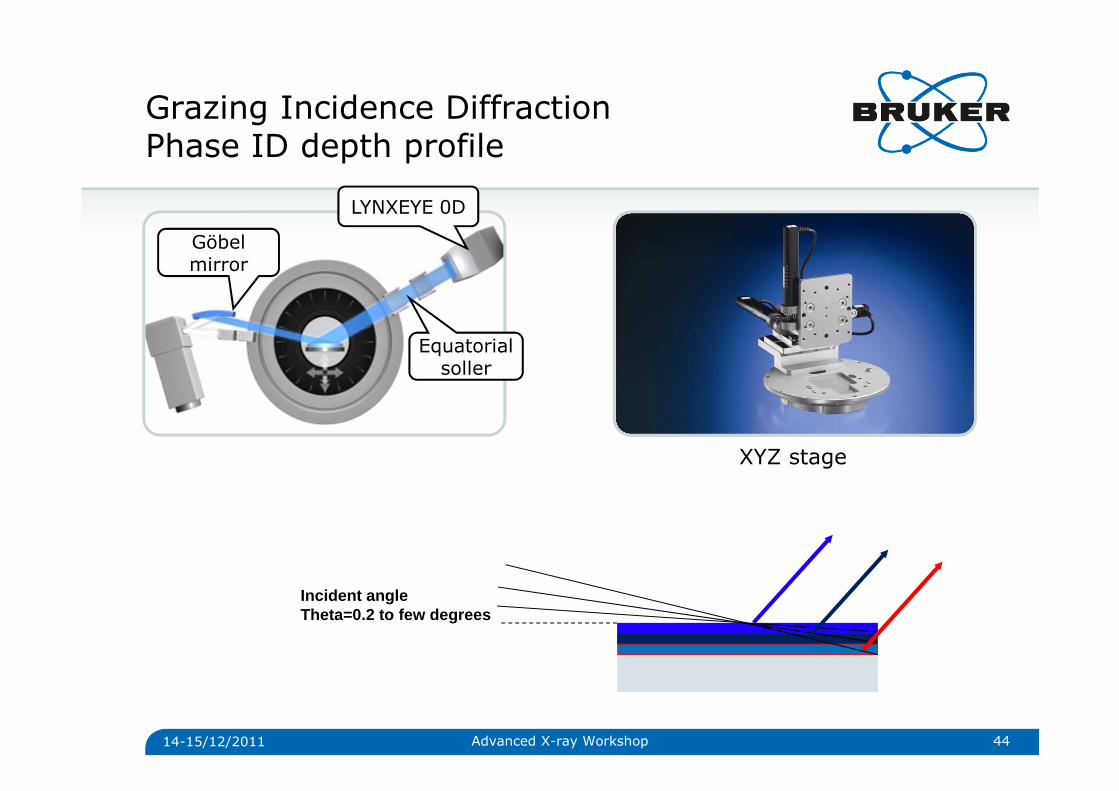
Incident angle Theta=0.2 to few degrees
Göbel mirror
Equatorial soller
LYNXEYE 0D
XYZ stage
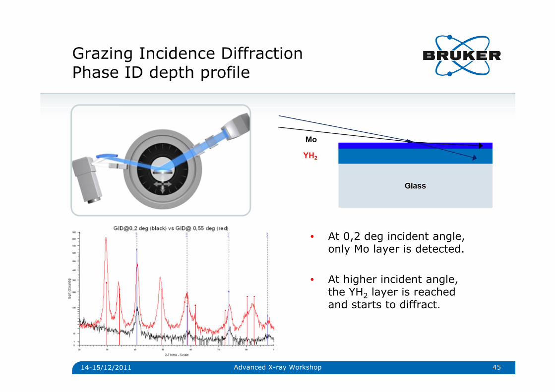
Grazing Incidence DiffractionPhase ID depth profile
Advanced X-ray Workshop
14-15/12/2011 45
• At 0,2 deg incident angle, only Mo layer is detected.
• At higher incident angle, the YH2 layer is reached and starts to diffract.
Grazing Incidence DiffractionPhase ID depth profile
Advanced X-ray Workshop
14-15/12/2011 46
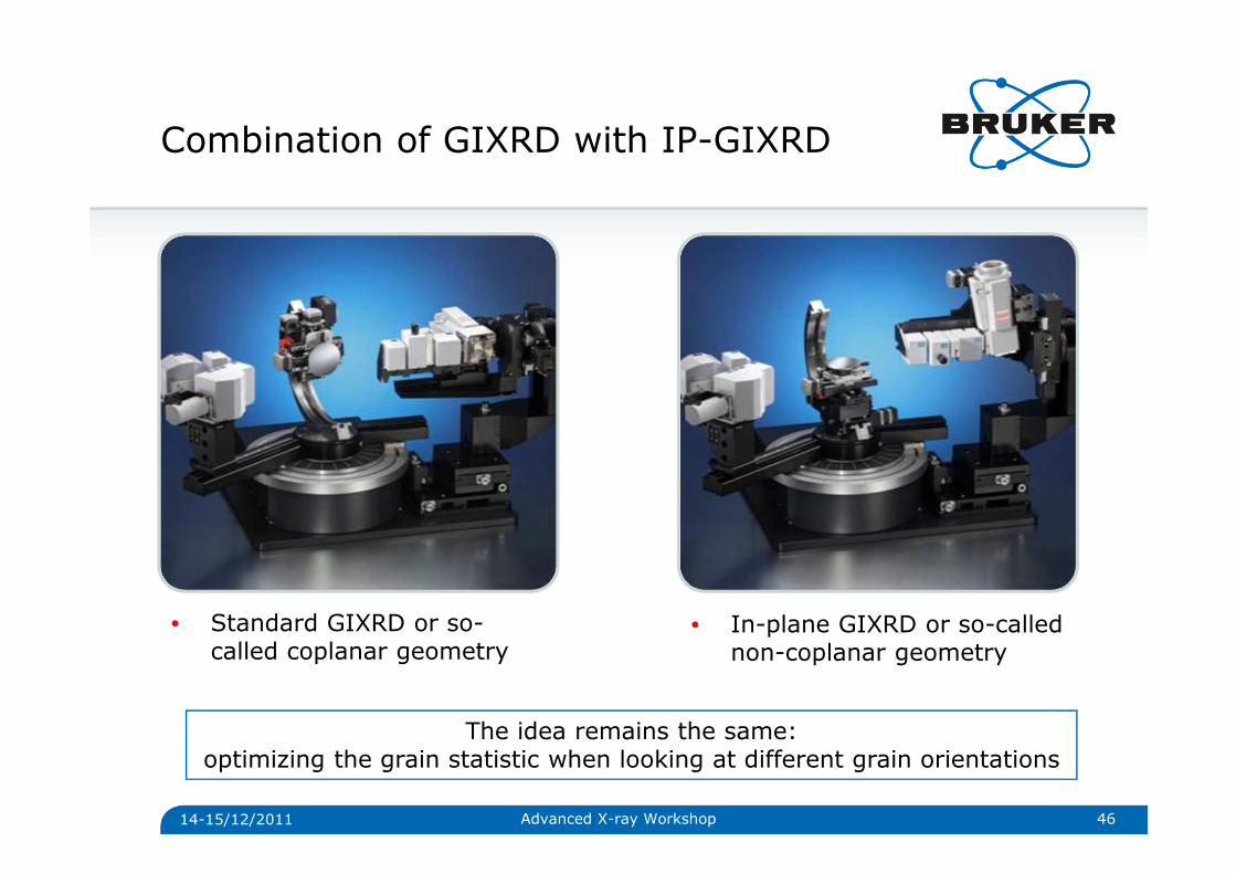
• Standard GIXRD or so-called coplanar geometry
• In-plane GIXRD or so-called non-coplanar geometry
The idea remains the same: optimizing the grain statistic when looking at different grain orientations
Combination of GIXRD with IP-GIXRD
Advanced X-ray Workshop
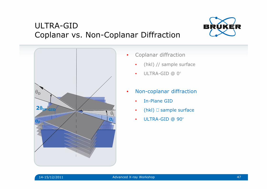
ULTRA-GIDCoplanar vs. Non-Coplanar Diffraction
14-15/12/2011 47Advanced X-ray Workshop
• Coplanar diffraction
• (hkl) // sample surface
• ULTRA-GID @ 0°
• Non-coplanar diffraction
• In-Plane GID
• (hkl) ⊥ sample surface
• ULTRA-GID @ 90°ααααiααααf
θθθθi
θθθθD
2θθθθIP-GID
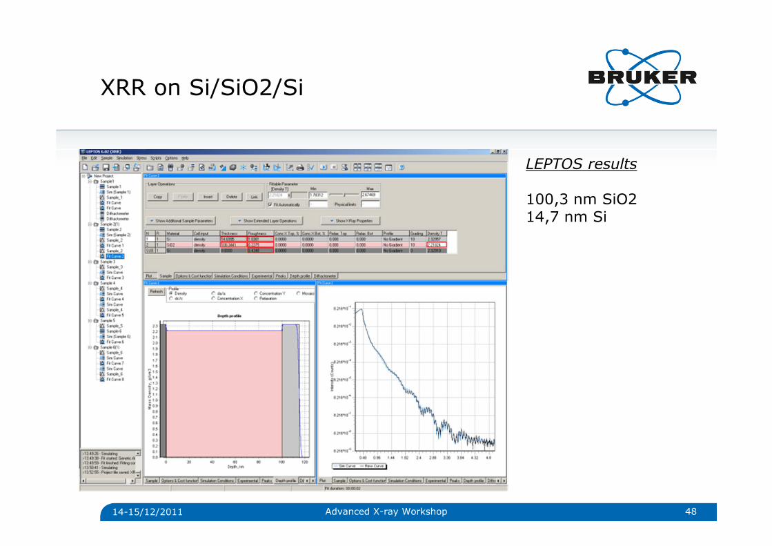
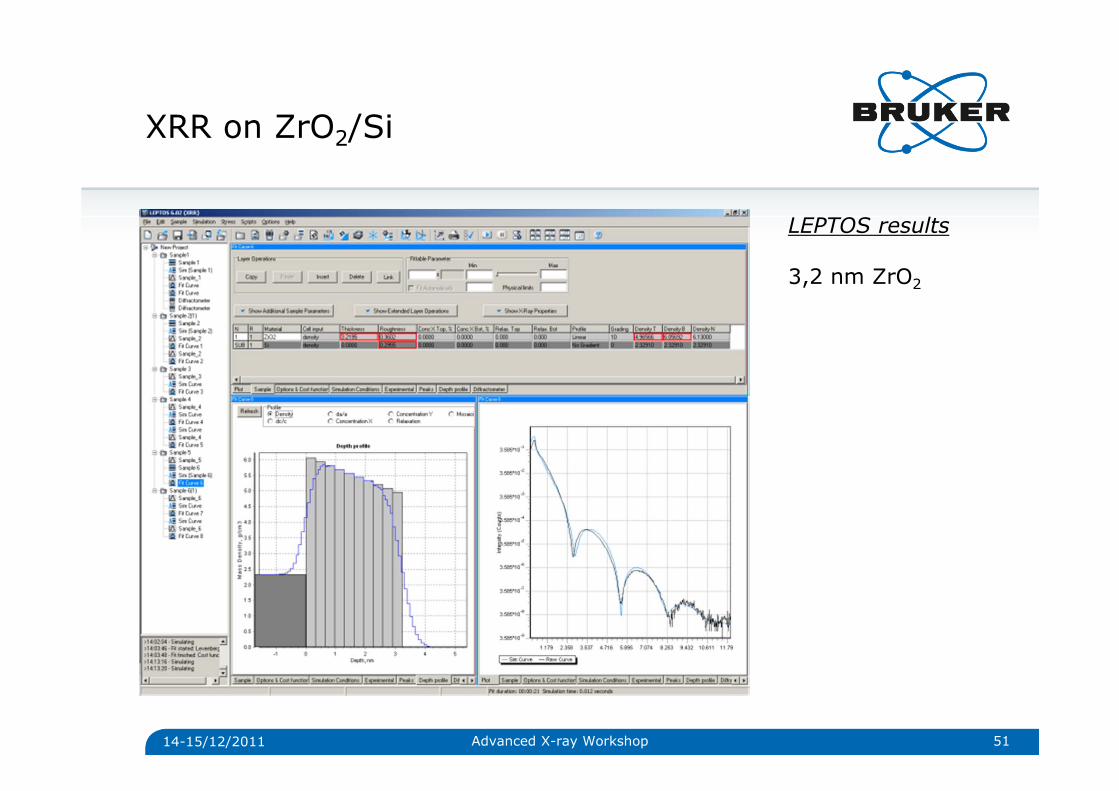
XRR on Si/SiO2/Si
14-15/12/2011 48
LEPTOS results
100,3 nm SiO214,7 nm Si
Advanced X-ray Workshop
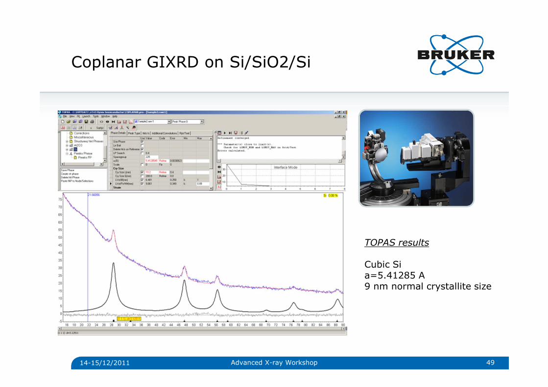
Coplanar GIXRD on Si/SiO2/Si
14-15/12/2011 49
TOPAS results
Cubic Si a=5.41285 A9 nm normal crystallite size
Advanced X-ray Workshop
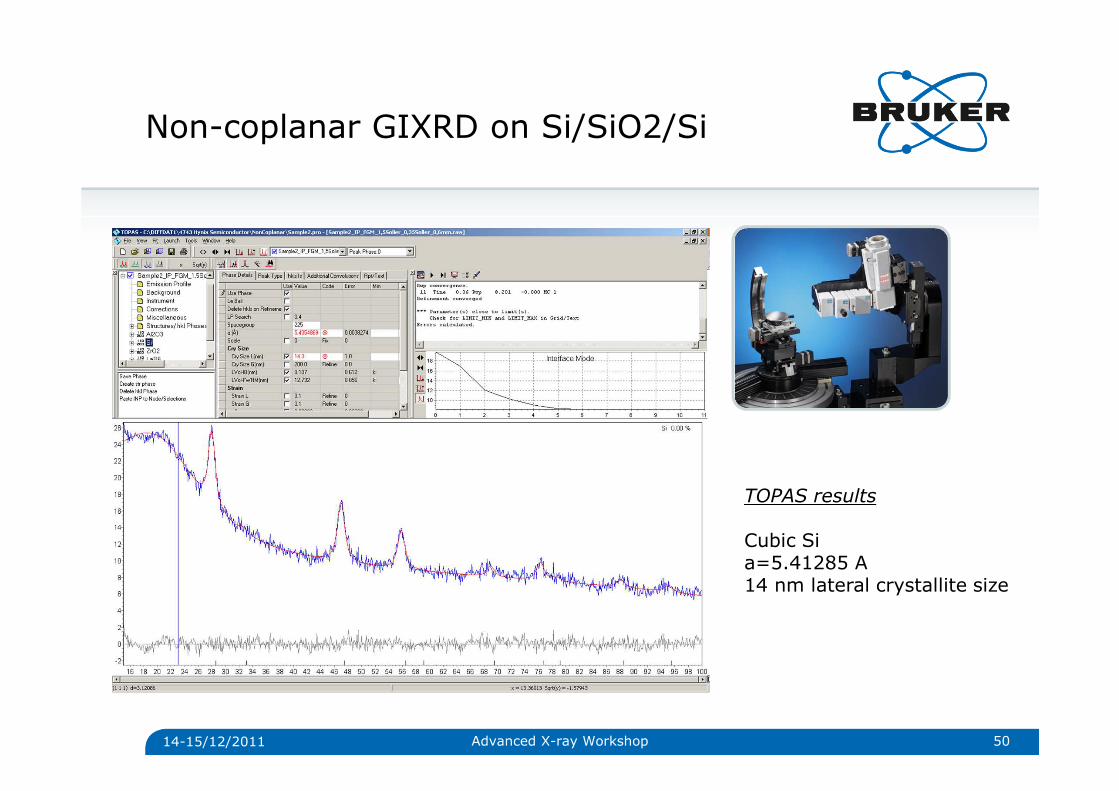
Non-coplanar GIXRD on Si/SiO2/Si
14-15/12/2011 50
TOPAS results
Cubic Si a=5.41285 A14 nm lateral crystallite size
Advanced X-ray Workshop
XRR on ZrO2/Si
14-15/12/2011 51
LEPTOS results
3,2 nm ZrO2
Advanced X-ray Workshop
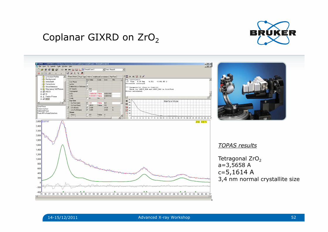
Coplanar GIXRD on ZrO2
14-15/12/2011 52
TOPAS results
Tetragonal ZrO2a=3,5658 Ac=5,1614 A3,4 nm normal crystallite size
Advanced X-ray Workshop

Non-coplanar GIXRD on ZrO2
14-15/12/2011 53
TOPAS results
Tetragonal ZrO2a=3,5994 Ac=5,18424 A30,4 nm lateral crystallite size
Advanced X-ray Workshop
Thin Film XRD MethodsParameters of Interest
14-15/12/2011 54Bruker Confidential
High-Resolution
X-Ray Diffraction
• thickness• lattice parameter• lattice mismatch• composition• strain & relaxation• lateral structure• mosaicity (crystallinity)• defects
X-Ray Reflectometry
• layer thickness• composition• roughness• density• porosity
Reciprocal Space
Mapping
• lattice parameter• lattice mismatch• composition• orientation• relaxation• lateral structure
Stress and Texture
• orientation distribution• orientation quantification• residual stress• epitaxial relationship
Grazing incidence
Diffraction (GIXRD)
• depth dependent information• phase identification• lattice parameter• microstructure (size/strain)• residual stress
In-Plane GIXRD
• IP-lattice parameter• IP-crystallite size• IP-orientation• epitaxial relation
Advanced X-ray Workshop
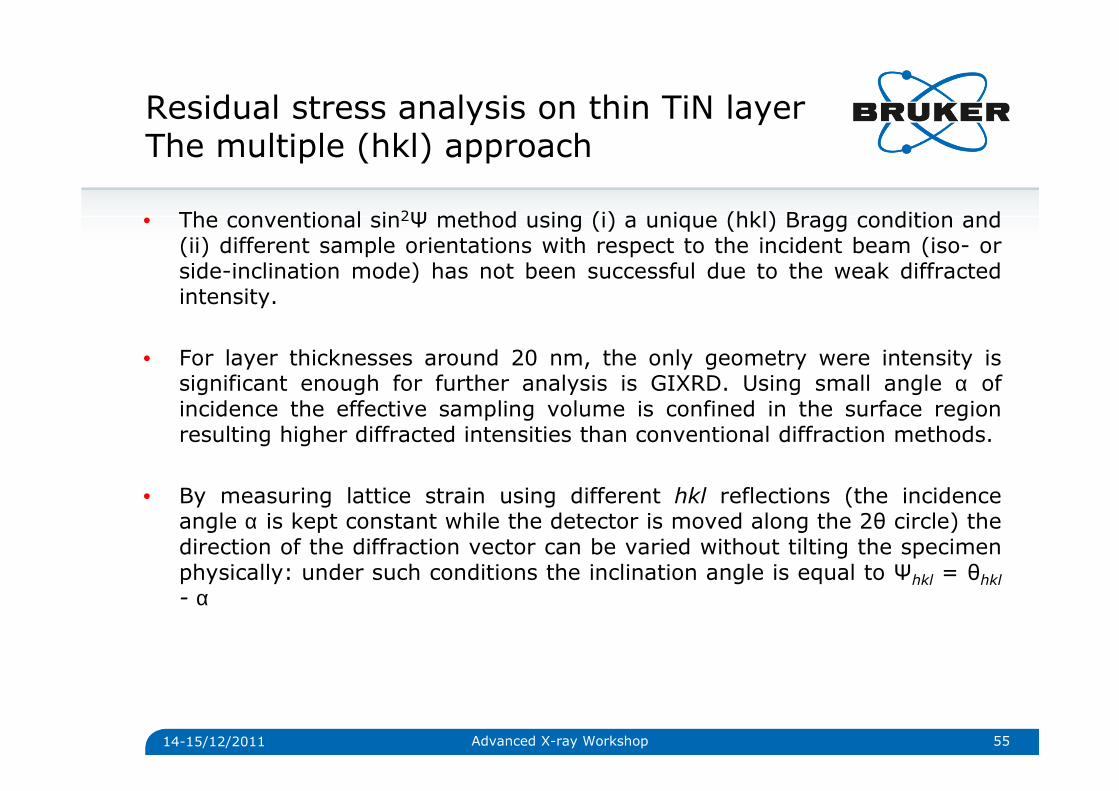
14-15/12/2011 55
• The conventional sin2Ψ method using (i) a unique (hkl) Bragg condition and(ii) different sample orientations with respect to the incident beam (iso- orside-inclination mode) has not been successful due to the weak diffractedintensity.
• For layer thicknesses around 20 nm, the only geometry were intensity issignificant enough for further analysis is GIXRD. Using small angle α ofincidence the effective sampling volume is confined in the surface regionresulting higher diffracted intensities than conventional diffraction methods.
• By measuring lattice strain using different hkl reflections (the incidenceangle α is kept constant while the detector is moved along the 2θ circle) thedirection of the diffraction vector can be varied without tilting the specimenphysically: under such conditions the inclination angle is equal to Ψhkl = θhkl- α
Residual stress analysis on thin TiN layerThe multiple (hkl) approach
Advanced X-ray Workshop
Experiments with D8 ADVANCE –Configuration of the diffractometer
14-15/12/2011 56
(*) A focusing Goebel mirror gives a lower penetration depth resolution, but a higher flux on the sample surface. If the customer has a focusing mirror for capillary measurements, he can definitely use it for GIXRD.
Goniometer D8 ADVANCE Theta/Theta
Measurementcircle
560 mm
Tube 2.2 kW Cu long fine focus
Tube power 40 kV / 40 mA
Primary opticsFocusing Goebel mirror (*)
0,4 mm exit slit
Sample stage XYZ stage with vacuum chuck
Secondary optics 0,4 deg equatorial Soller slit
DetectorScintillation counter or
LYNXEYE in 0D mode
Advanced X-ray Workshop
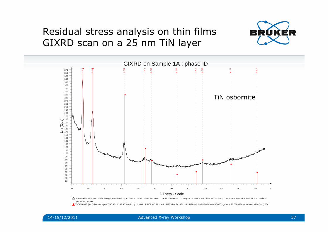
Residual stress analysis on thin filmsGIXRD scan on a 25 nm TiN layer
14-15/12/2011 57
GIXRD on Sample 1A : phase ID
03-065-4085 (I) - Osbornite, syn - TiN0.98 - Y: 99.90 % - d x by: 1. - WL: 1.5406 - Cubic - a 4.24190 - b 4.24190 - c 4.24190 - alpha 90.000 - beta 90.000 - gamma 90.000 - Face-centered - Fm-3m (225)Operations: ImportCommander Sample ID - File: GID@0,3245.raw - Type: Detector Scan - Start: 30.000000 ° - End: 146.00000 0 ° - Step: 0.100000 ° - Step time: 40. s - Temp.: 25 °C (Room) - Time Started: 0 s - 2-Theta:
Lin
(C
ps)
10
2030
4050
6070
8090
100110
120130
140150
160
170180
190200
210220
230240
250260
270
280290
300310
320330
340350
360370
2-Theta - Scale
30 40 50 60 70 80 90 100 110 120 130 140 150
[1,1
,1]
[2,0
,0]
[2,2
,0]
[3,1
,1]
[2,2
,2]
[4,0
,0]
[3,3
,1]
[4,2
,0]
[4,2
,2]
[5,1
,1]
TiN osbornite
Advanced X-ray Workshop
14-15/12/2011 58
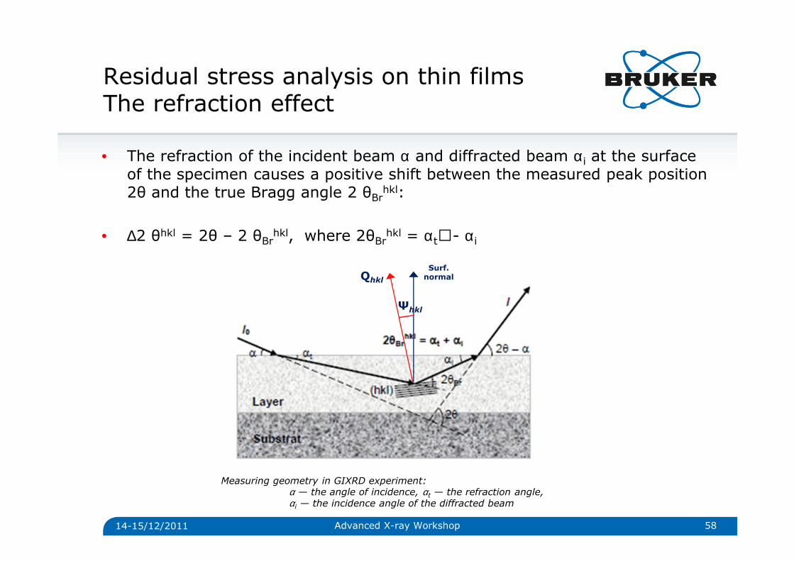
• The refraction of the incident beam α and diffracted beam αi at the surface of the specimen causes a positive shift between the measured peak position 2θ and the true Bragg angle 2 θBrhkl:
• ∆2 θhkl = 2θ – 2 θBrhkl, where 2θBrhkl = αt- αi
Measuring geometry in GIXRD experiment: α — the angle of incidence, αt — the refraction angle, αi — the incidence angle of the diffracted beam
Ψhkl
QhklSurf. normal
Residual stress analysis on thin filmsThe refraction effect
Advanced X-ray Workshop

14-15/12/2011 59
θC= 0.311 °
From Leptos fit: 25 nm TiN layer
Residual stress analysis on thin filmsXRR scan for critical angle determination
Advanced X-ray Workshop
14-15/12/2011 60
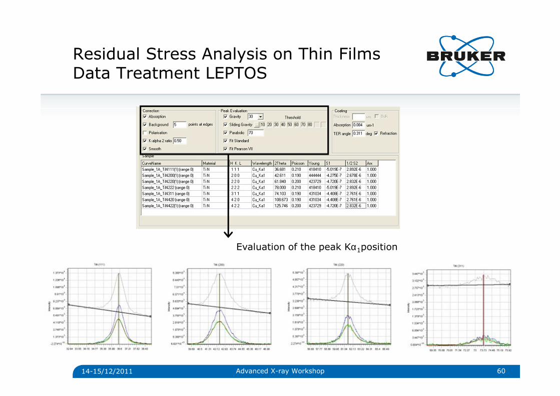
Evaluation of the peak Kα1position
Residual Stress Analysis on Thin FilmsData Treatment LEPTOS
Advanced X-ray Workshop
14-15/12/2011 61
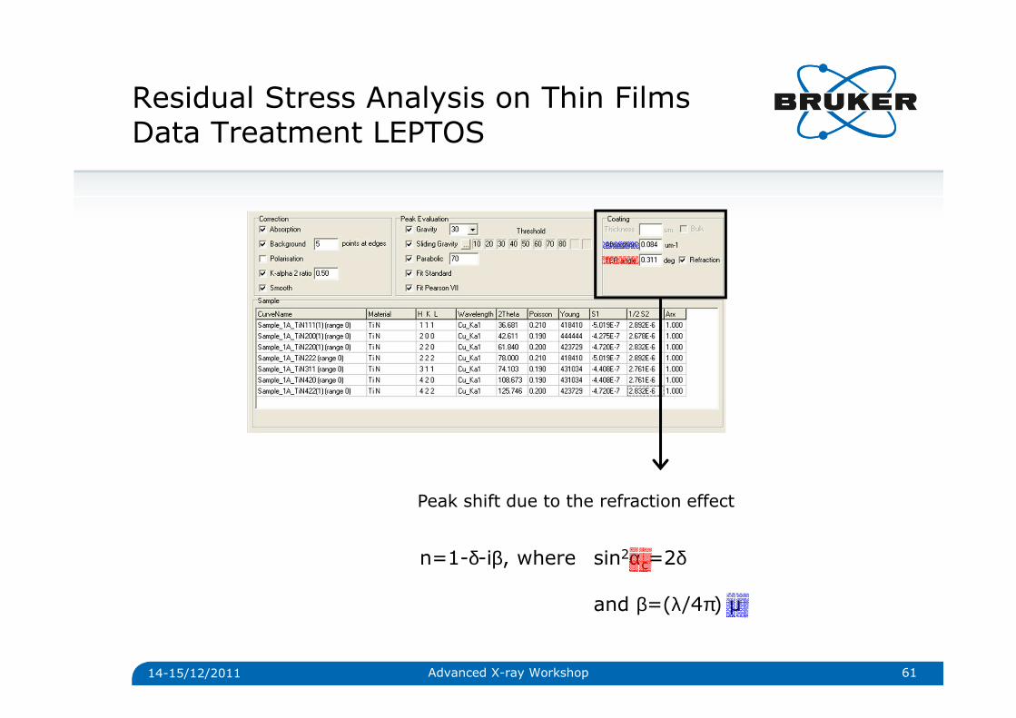
Peak shift due to the refraction effect
n=1-δ-iβ, where sin2αc=2δ
and β=(λ/4π) µ
Residual Stress Analysis on Thin FilmsData Treatment LEPTOS
Advanced X-ray Workshop
14-15/12/2011 62
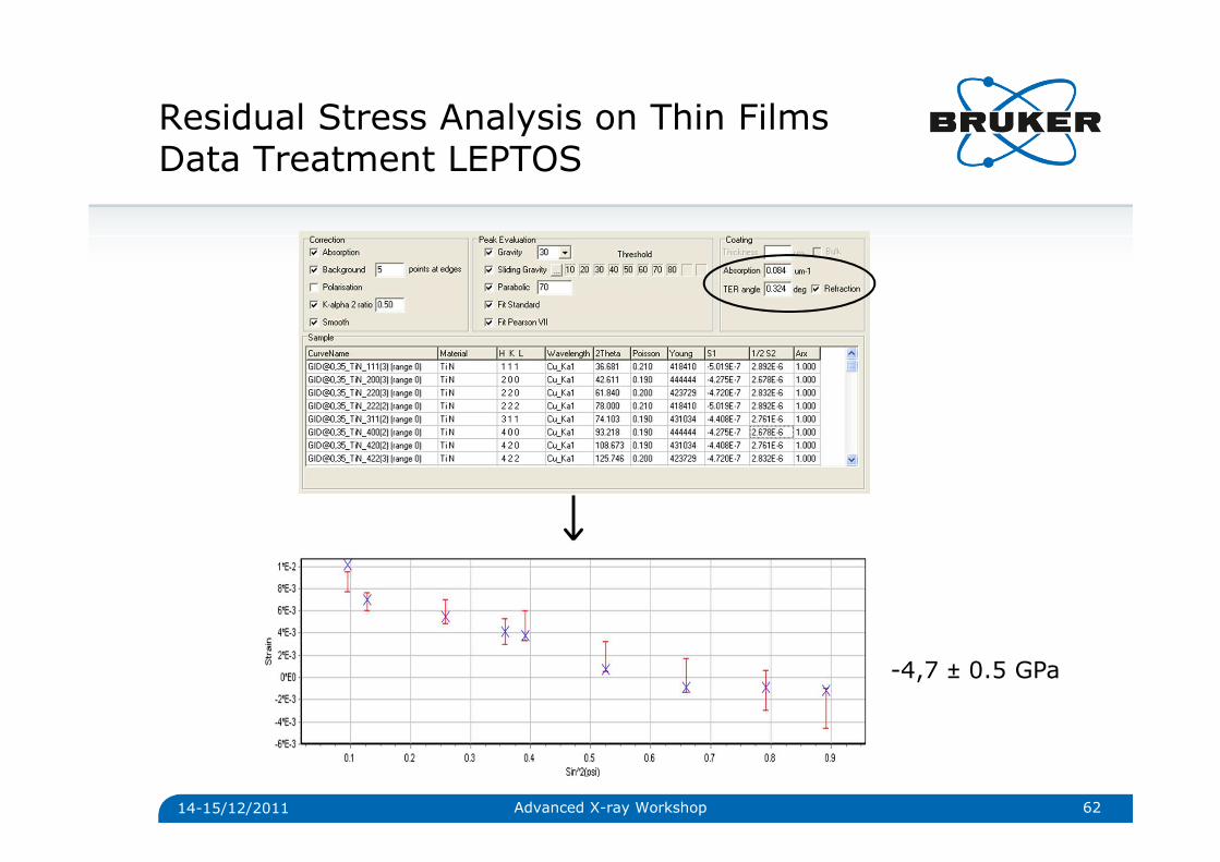
-4,7 ± 0.5 GPa
Residual Stress Analysis on Thin FilmsData Treatment LEPTOS
Advanced X-ray Workshop
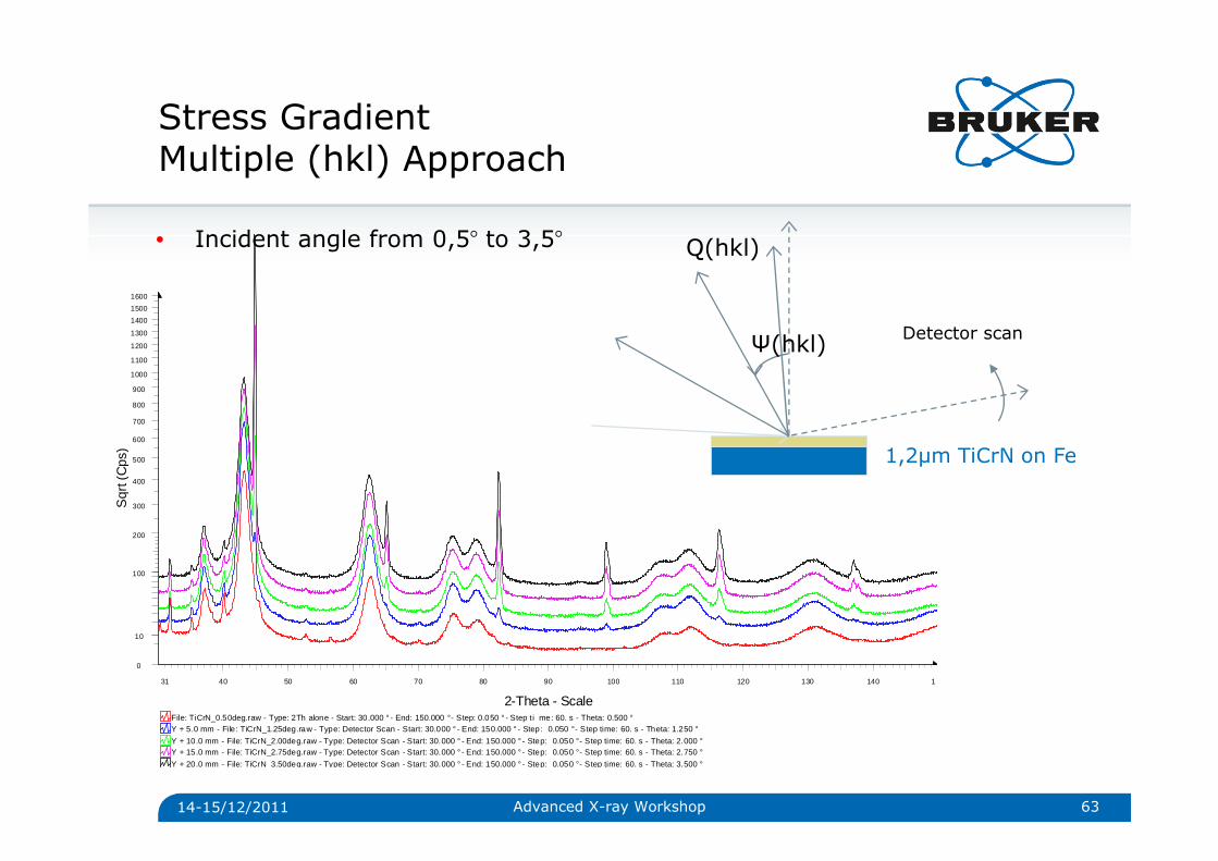
Y + 20.0 mm - File: TiCrN_3.50deg.raw - Type: Detector Scan - Start: 30.000 ° - End: 150.000 ° - Step: 0.050 ° - Step time: 60. s - Theta: 3.500 °
Y + 15.0 mm - File: TiCrN_2.75deg.raw - Type: Detector Scan - Start: 30.000 ° - End: 150.000 ° - Step: 0.050 ° - Step time: 60. s - Theta: 2.750 °Y + 10.0 mm - File: TiCrN_2.00deg.raw - Type: Detector Scan - Start: 30.000 ° - End: 150.000 ° - Step: 0.050 ° - Step time: 60. s - Theta: 2.000 °
Y + 5.0 mm - File: TiCrN_1.25deg.raw - Type: Detector Scan - Start: 30.000 ° - End: 150.000 ° - Step: 0.050 ° - Step time: 60. s - Theta: 1.250 °File: TiCrN_0.50deg.raw - Type: 2Th alone - Start: 30.000 ° - End: 150.000 ° - Step: 0.050 ° - Step t i me: 60. s - Theta: 0.500 °
Sqr
t (C
ps)
0
10
100
200
300
400
500
600
700
800
900
1000
1100
1200
1300
1400
1500
1600
2-Theta - Scale
31 40 50 60 70 80 90 100 110 120 130 140 150
14-15/12/2011 63
• Incident angle from 0,5° to 3,5°
1,2µm TiCrN on Fe
Detector scan
Q(hkl)
Ψ(hkl)
Stress GradientMultiple (hkl) Approach
Advanced X-ray Workshop

14-15/12/2011 64
• Incident angle from 0,5° to 3,5°
1,2µm TiCrN on Fe � Higher stress at the surface
Stress GradientMultiple (hkl) Approach
Advanced X-ray Workshop
14-15/12/2011 65
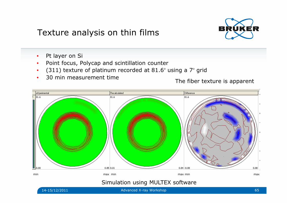
• Pt layer on Si• Point focus, Polycap and scintillation counter• (311) texture of platinum recorded at 81.6° using a 7° grid• 30 min measurement time
Texture analysis on thin films
min min min maxmaxmax
The fiber texture is apparent
Simulation using MULTEX softwareAdvanced X-ray Workshop

14-15/12/2011 66
As measured Simulated Residual
(220)
(422)
(111)
TiN pole figure simulation using MULTEX
Point focus, POLYCAP andscintillation counter
Texture analysis on thin films
Advanced X-ray Workshop

Innovation with Integrity
© Copyright Bruker Corporation. All rights reserved.14-15/12/2011 6715. Dezember 2011 67© Copyright Bruker Corporation. All rights reserved