Embed Size (px)
Citation preview
applied sciences
Article
Thin CdTe Layers Deposited by a Chamberless InlineProcess using MOCVD, Simulation and Experiment
Shafiul Monir 1, Giray Kartopu 2, Vincent Barrioz 3, Dan Lamb 2 , Stuart J. C. Irvine 2,Xiaogang Yang 4 and Yuriy Vagapov 1,*
1 Faculty of Art, Science and Technology, Wrexham Glyndwr University, Plas Coch, Mold Road,Wrexham LL11 2AW, UK; [email protected]
2 Centre for Solar Energy Research, College of Engineering, Swansea University, OpTIC Centre, St. AsaphBusiness Park, St. Asaph LL17 0JD, UK; [email protected] (G.K.);[email protected] (D.L.); [email protected] (S.J.C.I.)
3 Department of Mathematics, Physics and Electrical Engineering, Northumbria University, Ellison Building,Newcastle Upon Tyne NE1 8ST, UK; [email protected]
4 Faculty of Science and Engineering, University of Nottingham Ningbo, Sir Peter Mansfield Building,199 Taikang East Road, Ningbo 315100, China; [email protected]
* Correspondence: [email protected]
Received: 14 December 2019; Accepted: 11 February 2020; Published: 3 March 2020�����������������
Abstract: The deposition of thin Cadmium Telluride (CdTe) layers was performed by a chamberlessmetalorganic chemical vapour deposition process, and trends in growth rates were compared withcomputational fluid dynamics numerical modelling. Dimethylcadmium and diisopropyltelluridewere used as the reactants, released from a recently developed coating head orientated above theglass substrate (of area 15 × 15 cm2). Depositions were performed in static mode and dynamicmode (i.e., over a moving substrate). The deposited CdTe film weights were compared against thecalculated theoretical value of the molar supply of the precursors, in order to estimate materialutilisation. The numerical simulation gave insight into the effect that the exhaust’s restricted floworifice configuration had on the deposition uniformity observed in the static experiments. It wasshown that > 59% of material utilisation could be achieved under favourable deposition conditions.The activation energy determined from the Arrhenius plot of growth rate was ~ 60 kJ/mol and wasin good agreement with previously reported CdTe growth using metalorganic chemical vapourdeposition (MOCVD). Process requirements for using a chamberless environment for the inlinedeposition of compound semiconductor layers were presented.
Keywords: CFD modelling; chamberless inline process (CIP); MOCVD; cadmium telluride
1. Introduction
The growth rate of thin-film Cadmium Telluride (CdTe) using metalorganic chemical vapourdeposition (MOCVD) has been found to be sensitive to both substrate temperature and reactantpartial pressures [1], presenting a complex transport and kinetic process. Among the variousdeposition techniques used for CdTe growth, MOCVD is a favourable method, allowing control of themicrostructure and stoichiometry of the films [2–4]. MOCVD is an attractive method for depositingCdTe and another group II-VI compound semiconductor thin films [5,6]. It has been conventionallyassociated with a low-pressure batch process for the fabrication of optoelectronic devices [7], includingmulti-junction III-V photovoltaic cells for space applications [8]. Physical vapour deposition (PVD)techniques, such as closed-space sublimation (CSS) [9] or vapour transport deposition (VTD), are morecommonly used for the deposition of thin-film CdTe for photovoltaic (PV) applications. For example,
Appl. Sci. 2020, 10, 1734; doi:10.3390/app10051734 www.mdpi.com/journal/applsci

Appl. Sci. 2020, 10, 1734 2 of 12
First Solar has achieved a low production cost of ~$0.49 per watt using VTD for commercial CdTe PVmodules [10], whereas the efficiency has been increased to 21%, as reported by Green et al. [11]. SincePVD techniques are generally associated with vacuum processing, an alternative non-vacuum andscalable deposition processes, such as chamberless MOCVD, are desirable. Material utilisation of 40%for MOCVD of CdTe and conversion efficiency exceeding 11% for the fabricated CdTe solar cell deviceshave already been demonstrated using an inline reactor design [12,13].
Gas flow behaviour has a significant impact on the uniformity and reproducibility of coatingsproduced by MOCVD. In a previous paper, we reported the modelling of a vertical low-pressureMOCVD reactor geometry [14], providing an understanding of the film growth mechanism andcomplex chemical reactions.
Our group used computational fluid dynamics (CFD) modelling in the development of the coatinghead [15] for the chamberless coating setup described in the present paper. In a precursor to the workreported in this paper, Yang et al. [16] conducted three-dimensional (3D) simulations using CFD code –Fluent, investigating the effects of various conditions on CdTe film growth in an inline MOCVD reactor,where precursor gas flows were delivered normally to the direction of substrate translation. There,the sequential reactions involved in the CdTe deposition process were significantly simplified by theadoption of a proposed global surface reaction.
This paper focused on two aspects of our chamberless inline MOCVD process: (1) the influence andoptimisation of the exhaust restricted flow orifice (RFO) configuration, related to the deposition profilein static mode (i.e., on a stationary substrate), and (2) the effects of key deposition parameters on thepyrolysis of CdTe in the dynamic mode (i.e., on a moving substrate), including substrate temperature(Ts), precursor concentration (Pcon) and total gas flow (Ftotal). The deposition profiles, measured filmthicknesses and material (chemical precursor) utilisation were correlated to CFD simulations.
2. Experimental Section
The experiments were carried out using a chamberless inline system, incorporating 6 individualcoating heads capable of depositing different materials by MOCVD [17]. A single coating head on thissystem was used to deposit the CdTe layers reported in this work. Precursor gas flows were releasedfrom the coating head normal to the glass substrate being deposited on. The coating head consists of aprecursor delivery system, surrounded by containment curtain flows (CCF) and a balanced flow exhaustsystem, which is pressure and flow controlled by a combination of regulated extraction and individualRFOs positioned around the deposition zone of the coating head [15]. Figure 1 shows a projectionview of these components in the plane of substrate deposition, along with Figure 2 showing theover-layer grid system used for the analysis of deposition characteristics in static and dynamic modes.The chemical precursors used were dimethylcadmium (DMCd) and diisopropyltelluride (DIPTe) forcadmium (Cd) and tellurium (Te), respectively. High purity hydrogen (H2) gas (99.995%) was usedfor the main carrier gas, and nitrogen (N2) gas (99.9995%) was used for CCF. The heated stage wasmotion controlled and able to be positioned under any 1 of the 6 coating heads. Heating was achievedthrough infrared quartz elements radiating toward a graphite susceptor upon which the glass samplewas mounted. The stainless steel surface temperatures of the coating head and the heated stage weremaintained at 20–30 ◦C by using a closed-loop water cooling system. The temperature on the substrate’ssurface corresponded to the average surface temperature measured during temperature calibration(Figure 3). The set-point temperature from the controller was compared with the averaged measuredsubstrate surface temperature (from 3 different areas) and was within ±10 ◦C over a 15 × 15 cm2 areacentrally located on the heated zone.

Appl. Sci. 2020, 10, 1734 3 of 12Appl. Sci. 2020, 10, x FOR PEER REVIEW 3 of 11
- -
- -
Figure 1. Schematic representation of the coating head components [15]. The dashed edges (a–d)
represent the containment curtain flows (CCF), the single solid line represents the precursor delivery,
the dark solid grey shaded line represents the flow guide plate, the hashed square represents the
active exhaust, surrounding the deposition area, and the black dots (RFO-A and RFO-B) represent the
extraction points. The discontinuous light grey band represents the substrate width, while the central
arrow indicates the direction of travel [17]. RFO: restricted flow orifice. Reproduced with permission
from MOCVD for solar cells, a transition towards a chamberless inline process; published by Elsevier,
2015.
Figure 2. Schematic representation of the over-layer grid system used for analysis on the substrate
plane. Note that the dashed line is the “over-layer grid system” and only a guide to the eye for the
profilometry measuring points.
Figure 1. Schematic representation of the coating head components [15]. The dashed edges (a–d)represent the containment curtain flows (CCF), the single solid line represents the precursor delivery,the dark solid grey shaded line represents the flow guide plate, the hashed square represents theactive exhaust, surrounding the deposition area, and the black dots (RFO-A and RFO-B) representthe extraction points. The discontinuous light grey band represents the substrate width, while thecentral arrow indicates the direction of travel [17]. RFO: restricted flow orifice. Reproduced withpermission from MOCVD for solar cells, a transition towards a chamberless inline process; publishedby Elsevier, 2015.
Appl. Sci. 2020, 10, x FOR PEER REVIEW 3 of 11
- -
- -
Figure 1. Schematic representation of the coating head components [15]. The dashed edges (a–d)
represent the containment curtain flows (CCF), the single solid line represents the precursor delivery,
the dark solid grey shaded line represents the flow guide plate, the hashed square represents the
active exhaust, surrounding the deposition area, and the black dots (RFO-A and RFO-B) represent the
extraction points. The discontinuous light grey band represents the substrate width, while the central
arrow indicates the direction of travel [17]. RFO: restricted flow orifice. Reproduced with permission
from MOCVD for solar cells, a transition towards a chamberless inline process; published by Elsevier,
2015.
Figure 2. Schematic representation of the over-layer grid system used for analysis on the substrate
plane. Note that the dashed line is the “over-layer grid system” and only a guide to the eye for the
profilometry measuring points.
Figure 2. Schematic representation of the over-layer grid system used for analysis on the substrateplane. Note that the dashed line is the “over-layer grid system” and only a guide to the eye for theprofilometry measuring points.

Appl. Sci. 2020, 10, 1734 4 of 12Appl. Sci. 2020, 10, x FOR PEER REVIEW 4 of 11
Figure 3. Controller temperature set-point vs averaged measured substrate surface temperature.
CdTe layers were deposited on 3 mm thick 20 × 30 cm2 NeoceramTM (Ceramic Glass Ltd.,
Loughborough, England) type glass rectangles for static mode operation. The area and coverage of
the deposited (Adep) layers were assessed over the central 15 cm × 15 cm area using the over-layer grid
system shown in Figure 2 (static), by which any spread in the deposited film thickness and the
deposited volume (vexp) of the material was determined. The material utilisation (Uvmat) was calculated
using Equation (1).
exp
100%mat
theor
vUv
v (1)
where vexp was calculated using:
exp dep
v d A (2)
where d is the average film thickness, Adep is the deposited area, νtheor is the theoretical volume of CdTe
deposit, limited by the molar supply of the metal-organic precursor [10], which was calculated using
the relationship
3
0
22.4 4mo mo d A
theor
p F t N av (3)
where pmo and Fmo are the partial pressures and the mass flow rate, respectively, of the limiting
precursor (DiPTe in this series of experiments), td is the deposition time, NA is the Avagadro constant,
a0 is the lattice constant of CdTe (6.48 Å ). The RFO diameters were varied from 0.5 to 1.0 mm, and the
differential pressure of the active exhaust was controlled from −5 to −15 Torr (relative to ambient
pressure).
For the dynamic mode experiments, CdTe layers were deposited on 3.2 mm thick 15 × 15 cm2
TECTM C15 glass substrates provided by NSG Pilkington (Nippon Sheet Glass Co Ltd., Mita Minato-
ku, Tokyo), moving at a translation speed (vsub) of 1.8 cm/min. The mass deposit (mexp) and d were
measured from a 5 × 5 cm2 specimen cut out from the centre of the substrate after deposition, due to
the size restriction on the micro-balance used. The material utilisation based on gravimetric
measurements (Uwmat) was calculated from:
exp
100%mat
theor
mUw
m (4)
The resolution of the measured mass mexp was 0.1 mg (micro-balance resolution). The theoretical
mass (mtheor) of the deposit was calculated using:
250
300
350
400
450
500
550
250 300 350 400 450 500 550 600 650
Sub
stra
te S
urf
ace
Te
mp
era
ture
(°C
)
TControl Set-Point (°C)
Figure 3. Controller temperature set-point vs averaged measured substrate surface temperature.
CdTe layers were deposited on 3 mm thick 20 × 30 cm2 NeoceramTM (Ceramic Glass Ltd.,Loughborough, England) type glass rectangles for static mode operation. The area and coverage ofthe deposited (Adep) layers were assessed over the central 15 cm × 15 cm area using the over-layergrid system shown in Figure 2 (static), by which any spread in the deposited film thickness and thedeposited volume (vexp) of the material was determined. The material utilisation (Uvmat) was calculatedusing Equation (1).
Uvmat =vexp
vtheor× 100% (1)
where vexp was calculated using:vexp = d×Adep (2)
where d is the average film thickness, Adep is the deposited area, νtheor is the theoretical volume of CdTedeposit, limited by the molar supply of the metal-organic precursor [10], which was calculated usingthe relationship
vtheor =pmoFmotdNA
22.4×
a30
4(3)
where pmo and Fmo are the partial pressures and the mass flow rate, respectively, of the limitingprecursor (DiPTe in this series of experiments), td is the deposition time, NA is the Avagadro constant,a0 is the lattice constant of CdTe (6.48 Å). The RFO diameters were varied from 0.5 to 1.0 mm, and thedifferential pressure of the active exhaust was controlled from −5 to −15 Torr (relative to ambientpressure).
For the dynamic mode experiments, CdTe layers were deposited on 3.2 mm thick 15 × 15 cm2
TECTM C15 glass substrates provided by NSG Pilkington (Nippon Sheet Glass Co Ltd., Mita Minato-ku,Tokyo), moving at a translation speed (vsub) of 1.8 cm/min. The mass deposit (mexp) and d weremeasured from a 5 × 5 cm2 specimen cut out from the centre of the substrate after deposition, due to thesize restriction on the micro-balance used. The material utilisation based on gravimetric measurements(Uwmat) was calculated from:
Uwmat =mexp
mtheor× 100% (4)
The resolution of the measured mass mexp was 0.1 mg (micro-balance resolution). The theoreticalmass (mtheor) of the deposit was calculated using:
mtheor = vtheor × ρCdTe (5)

Appl. Sci. 2020, 10, 1734 5 of 12
with ρCdTe being the density of CdTe (5.86 g/cm3 at 25 ◦C) [18]. In these experiments, the depositionsurface temperature (Ts) was varied between 305 ◦C and 470 ◦C, the precursor concentrations (i.e., partialpressures) were varied from 1.38 to 3.48 Torr for DMCd and 0.44 to 1.08 Torr for DiPTe, and FTotal from0.5 to 1.0 L/min.
The layer thicknesses in static and dynamic modes were measured using a Veeco Dektak 150(Veeco Instruments Inc. Planview, New York, United Staes) stylus profilometer over the available datapoints (Figure 2). The dynamic growth rates (GR) given were determined using the averaged finalthickness in relation to the time of deposition, td (i.e., duration of substrate passing through the activedeposition zone).
3. Numerical Modelling
Simplified 2D and 3D models of the coating head delivery system were developed, using acombined mesh not exceeding 100,000 cells for 2D and 700,000 cells for 3D to define the numericalmodel. In order to correlate simulation with experimental data, a surface chemical reaction wasapplied for the 2D model for simplification. The 3D model employed H2 and N2 as the mass species,presenting the deposition profile of H2 on the substrate, determined by the CCF, RFO configurationand active exhaust extraction. A finer mesh, in the vicinity of the substrate, was employed to accountfor the influence of the temperature gradient and boundary layer formation. A no-slip boundarycondition was prescribed on the domain walls, the exit of the system (i.e., exhaust) was defined asoutflow, while the velocity out of the injector was defined as inlet velocity (i.e., based on total flowrate). In addition, any experimental apparatus walls that were controlled by water cooling wereapproximated as isothermal walls within the numerical models. A constant temperature conditionwas applied to the substrate surface. Pressure-velocity coupling was obtained using the SIMPLE [19]algorithm, with the discretisation scheme for pressure being second-order. To ensure stability, themomentum, energy and chemical species transport were set to first-order upwind. In order to derive thedifferential equations for expressing conservation of mass, momentum and energy, some assumptionswere made: (1) the gas mixture is a continuum; (2) gas flows are laminar; (3) steady-state conditionsprevail; (4) the equation of state obeys the ideal gas law. Under these assumptions, the differentialequations were simplified as by Yang et al. [16]. Further, due to the lack of detailed chemical dataregarding the deposition of CdTe thin film from the gas mixture, one overall surface chemical reactionon the substrate was considered [16]:
DIPTe(g) + DMCd(g) + H2 → CdTe(s) + Res(g) (6)
where Res(g) represents all the by-products of the reaction. The following Arrhenius expression wasused to express the rate of the reaction:
k = ATβe−EaRT (7)
where A is the pre-exponential factor, which relates to the reaction frequency between the precursormolecules, Ea is the activation energy to initiate the reaction, R is the universal gas constant (8313J/K·mol) and β is the temperature exponent. The pre-exponential factor was set to A ≈ 1016 s−1 [20],the temperature exponent βwas set to 0 and the activation energy Ea was set to 59.62 kJ·mol−1.
All simulations were conducted on a Fujitsu Celsius W510 ProGREEN workstation, with aQuad-Core Intel Xenon, 3.3 GHz and 16.0 GB RAM, running the commercial CFD software ANSYSFluent (ANSYS, Canonsburh, PA, USA).

Appl. Sci. 2020, 10, 1734 6 of 12
4. Results and Discussion
4.1. Static Mode – Deposition Profile
A series of CdTe thin films were grown with td = 20 min, Ts = 430 ◦C and FTotal = 0.5 L/min.In order to study the deposition profile behaviour, the RFO sizes and active exhaust were varied,as shown in Table 1.
Table 1. Parametric variables for static mode (locations of RFO-A and RFO-B are shown in Figure 1).
Configuration RFO Size (mm) Active Extraction(RFO-A) (RFO-B) (Torr)
S-1 0.5 0.7 −10S-2 0.7 0.5 −10S-3 0.7 0.5 −15S-4 1.0 0.5 −10
RFO - Restricted Flow Orifice.
The deposition profiles shown in Figure 4 highlighted that thin-film growth was stronglydependent on the RFO configuration. The change in the active exhaust from −10 to −15 Torr (S-2 toS-3) had very little impact on the material utilisation when compared with S-2. From CFD simulations,the velocity profile was obtained 8 mm upstream and downstream of the injector slit (Figure 5a).The configuration of RFOs in S-1 resulted in a greater flow direction downstream of the injector due tothe extraction being stronger with 0.7mm and 0.5mm RFOs in situ for RFO-A and RFO-B, respectively.However, by alternating the configuration, as in S-4, reduced the extraction strength downstream,resulting in a recirculating vortex located behind the injector slit and in front of the flow guide plate.The film thickness (d) data for the extreme cases (S-1 and S-4), presented in Figure 5b, confirmed thatthe deposited profile was narrower and the peak (maximum) film thickness was greater with S-4.This was expected to be related to the vortex generated near the flow guide plate compared with S-1,as seen in Figure 6a,b. Figure 6 only shows the exhaust located behind the injector RFO-A, the guideflow plate was located in this section and had a direct influence on the overall deposited layer due tothe presence of the recirculating vortex in S-4 RFO configuration. The downstream extraction point(RFO-B) had no direct influence or change in the fluid flow pattern and, therefore, only this exhaustis presented in Figure 6. The vortex provided an alternative route to increase residence time on thesurface of the substrate for the unreacted precursors to be recycled, therefore, increasing the materialutilisation, as shown in Figure 7. However, due to the recirculating vortex, the overall uniformity ofthe deposited layer was affected with such configuration. Therefore, S-1 configuration was chosen fordynamic mode analysis, depositing a larger uniform surface area.

Appl. Sci. 2020, 10, 1734 7 of 12
Appl. Sci. 2020, 10, x FOR PEER REVIEW 6 of 11
A series of CdTe thin films were grown with td = 20 min, Ts = 430 °C and FTotal = 0.5 l/min. In order
to study the deposition profile behaviour, the RFO sizes and active exhaust were varied, as shown in
Table 1.
Table 1. Parametric variables for static mode (locations of RFO-A and RFO-B are shown in Figure 1).
Configuration RFO Size (mm) Active Extraction
(RFO-A) (RFO-B) (Torr)
S-1 0.5 0.7 −10
S-2 0.7 0.5 −10
S-3 0.7 0.5 −15
S-4 1.0 0.5 −10
RFO - Restricted Flow Orifice.
The deposition profiles shown in Figure 4 highlighted that thin-film growth was strongly
dependent on the RFO configuration. The change in the active exhaust from −10 to −15 Torr (S-2 to S-
3) had very little impact on the material utilisation when compared with S-2. From CFD simulations,
the velocity profile was obtained 8 mm upstream and downstream of the injector slit (Figure 5a). The
configuration of RFOs in S-1 resulted in a greater flow direction downstream of the injector due to
the extraction being stronger with 0.7mm and 0.5mm RFOs in situ for RFO-A and RFO-B,
respectively. However, by alternating the configuration, as in S-4, reduced the extraction strength
downstream, resulting in a recirculating vortex located behind the injector slit and in front of the flow
guide plate. The film thickness (d) data for the extreme cases (S-1 and S-4), presented in Figure 5b,
confirmed that the deposited profile was narrower and the peak (maximum) film thickness was
greater with S-4. This was expected to be related to the vortex generated near the flow guide plate
compared with S-1, as seen in Figure 6a,b. Figure 6 only shows the exhaust located behind the injector
RFO-A, the guide flow plate was located in this section and had a direct influence on the overall
deposited layer due to the presence of the recirculating vortex in S-4 RFO configuration. The
downstream extraction point (RFO-B) had no direct influence or change in the fluid flow pattern and,
therefore, only this exhaust is presented in Figure 6. The vortex provided an alternative route to
increase residence time on the surface of the substrate for the unreacted precursors to be recycled,
therefore, increasing the material utilisation, as shown in Figure 7. However, due to the recirculating
vortex, the overall uniformity of the deposited layer was affected with such configuration. Therefore,
S-1 configuration was chosen for dynamic mode analysis, depositing a larger uniform surface area.
(a) (b) (c) (d)
Figure 4. Cadmium Telluride (CdTe) static deposition profiles from experimental samples (bottom)
and computational fluid dynamics (CFD) simulations (top). Deposition conditions varied from S-1 (a)
to S-4 (d) in sequence, as given in Table 1.
Figure 4. Cadmium Telluride (CdTe) static deposition profiles from experimental samples (bottom)and computational fluid dynamics (CFD) simulations (top). Deposition conditions varied from S-1 (a)to S-4 (d) in sequence, as given in Table 1.Appl. Sci. 2020, 10, x FOR PEER REVIEW 7 of 11
(a) (b)
Figure 5. (a) Flow velocity profile (m/s) 8 mm in the front and behind the precursor injector slit for S-
1–S-4 configurations. (b) Mapping of CdTe film thickness profiles obtained in static mode for
deposition conditions S-1 and S-4.
(a) (b)
Figure 6. Path lines located behind the precursor injector slit (i.e., near RFO-A in Figure 1) around the
flow guide plate and the exhaust (a) for S-1 and (b) for S-4.
Figure 7. Material utilisation calculated using (1) for S-1–S-4 configurations.
4.2. Dynamic Mode – Deposition Kinetics
A series of CdTe thin films were grown using the S-1 configuration, with FTotal = 1.0 l/min and
vsub = 1.8 cm/min, where only Ts was varied in order to correlate the kinetic regime of the pyrolysis of
CdTe layer with CFD simulations (Figure 8a). The activation energy (Ea) of the surface kinetic reaction
was calculated from Equation (8) using the linear range from the Arrhenius plot in Figure 8a.
1
-0.8-0.6-0.4-0.200.20.40.60.8
Co
atin
g H
ead
Hig
ht
(cm
)
Velocity Magnitude (m/s)
S-1
S-2
S-3
S-4
RFO-ARFO-B0.2
0.15
0.1
0.05
0
1
0
1000
2000
3000
4000
5000
6000
7000
0 1.5 3 4.5 6 7.5 9 10.5 12
Ave
rage
Film
Th
ickn
ess
(nm
)
Substrate length (cm)
S-1
S-4
39.48
41.6141.91
44.66
36
37
38
39
40
41
42
43
44
45
46
S-1 S-2 S-3 S-4
Ma
teri
al U
tiliz
atio
n (
%)
Figure 5. (a) Flow velocity profile (m/s) 8 mm in the front and behind the precursor injector slitfor S-1–S-4 configurations. (b) Mapping of CdTe film thickness profiles obtained in static mode fordeposition conditions S-1 and S-4.
Appl. Sci. 2020, 10, x FOR PEER REVIEW 7 of 11
(a) (b)
Figure 5. (a) Flow velocity profile (m/s) 8 mm in the front and behind the precursor injector slit for S-
1–S-4 configurations. (b) Mapping of CdTe film thickness profiles obtained in static mode for
deposition conditions S-1 and S-4.
(a) (b)
Figure 6. Path lines located behind the precursor injector slit (i.e., near RFO-A in Figure 1) around the
flow guide plate and the exhaust (a) for S-1 and (b) for S-4.
Figure 7. Material utilisation calculated using (1) for S-1–S-4 configurations.
4.2. Dynamic Mode – Deposition Kinetics
A series of CdTe thin films were grown using the S-1 configuration, with FTotal = 1.0 l/min and
vsub = 1.8 cm/min, where only Ts was varied in order to correlate the kinetic regime of the pyrolysis of
CdTe layer with CFD simulations (Figure 8a). The activation energy (Ea) of the surface kinetic reaction
was calculated from Equation (8) using the linear range from the Arrhenius plot in Figure 8a.
1
-0.8-0.6-0.4-0.200.20.40.60.8
Co
atin
g H
ead
Hig
ht
(cm
)
Velocity Magnitude (m/s)
S-1
S-2
S-3
S-4
RFO-ARFO-B0.2
0.15
0.1
0.05
0
1
0
1000
2000
3000
4000
5000
6000
7000
0 1.5 3 4.5 6 7.5 9 10.5 12
Ave
rage
Film
Th
ickn
ess
(nm
)
Substrate length (cm)
S-1
S-4
39.48
41.6141.91
44.66
36
37
38
39
40
41
42
43
44
45
46
S-1 S-2 S-3 S-4
Ma
teri
al U
tiliz
atio
n (
%)
Figure 6. Path lines located behind the precursor injector slit (i.e., near RFO-A in Figure 1) around theflow guide plate and the exhaust (a) for S-1 and (b) for S-4.

Appl. Sci. 2020, 10, 1734 8 of 12
Appl. Sci. 2020, 10, x FOR PEER REVIEW 7 of 11
(a) (b)
Figure 5. (a) Flow velocity profile (m/s) 8 mm in the front and behind the precursor injector slit for S-
1–S-4 configurations. (b) Mapping of CdTe film thickness profiles obtained in static mode for
deposition conditions S-1 and S-4.
(a) (b)
Figure 6. Path lines located behind the precursor injector slit (i.e., near RFO-A in Figure 1) around the
flow guide plate and the exhaust (a) for S-1 and (b) for S-4.
Figure 7. Material utilisation calculated using (1) for S-1–S-4 configurations.
4.2. Dynamic Mode – Deposition Kinetics
A series of CdTe thin films were grown using the S-1 configuration, with FTotal = 1.0 l/min and
vsub = 1.8 cm/min, where only Ts was varied in order to correlate the kinetic regime of the pyrolysis of
CdTe layer with CFD simulations (Figure 8a). The activation energy (Ea) of the surface kinetic reaction
was calculated from Equation (8) using the linear range from the Arrhenius plot in Figure 8a.
1
-0.8-0.6-0.4-0.200.20.40.60.8
Co
atin
g H
ead
Hig
ht
(cm
)
Velocity Magnitude (m/s)
S-1
S-2
S-3
S-4
RFO-ARFO-B0.2
0.15
0.1
0.05
0
1
0
1000
2000
3000
4000
5000
6000
7000
0 1.5 3 4.5 6 7.5 9 10.5 12
Ave
rage
Film
Th
ickn
ess
(nm
)
Substrate length (cm)
S-1
S-4
39.48
41.6141.91
44.66
36
37
38
39
40
41
42
43
44
45
46
S-1 S-2 S-3 S-4
Ma
teri
al U
tiliz
atio
n (
%)
Figure 7. Material utilisation calculated using (1) for S-1–S-4 configurations.
4.2. Dynamic Mode – Deposition Kinetics
A series of CdTe thin films were grown using the S-1 configuration, with FTotal = 1.0 L/min andvsub = 1.8 cm/min, where only Ts was varied in order to correlate the kinetic regime of the pyrolysis ofCdTe layer with CFD simulations (Figure 8a). The activation energy (Ea) of the surface kinetic reactionwas calculated from Equation (8) using the linear range from the Arrhenius plot in Figure 8a.
ln(GR) = ln(A) −Ea
RTs(8)
where GR is the growth rate, and R is the gas constant (8.314 J/K·mol).
Appl. Sci. 2020, 10, x FOR PEER REVIEW 8 of 11
ln ln a
s
EGR A
RT (8)
where GR is the growth rate, and R is the gas constant (8.314 J/K·mol).
Saturation of GR was observed for Ts > 420 °C; therefore, the linear region in the lower
temperature range was used to calculate Ea, with a value of 59.62 kJ/mol. This appeared to be
somewhat larger than the results experimentally obtained by Barrioz et al. [12] (49 kJ/mol) for a
slightly larger VI:II precursor ratio for deposition in an enclosed inline MOCVD reactor (Figure 8b).
Barrioz et al. [12] also observed saturation in GR at higher temperatures (i.e., >405 °C), attributed to
mass transport limitation due to the Te precursor’s concentration. Despite the slightly higher
activation energy, the activation energy as a function of VI:II ratio followed the trend observed by
previous authors [12,21] within experimental errors.
Using the S-1 configuration, a series of CdTe thin films were grown for FTotal = 0.5 l/min and
FTotal = 1.0 l/min while maintaining the precursor partial pressures constant at DMCd = 3.48 Torr and
DIPTe = 1.08 Torr, vsub = 1.8 cm/min, while varying Ts (Table 2).
1
10
100
1000
10000
0.0012 0.0014 0.0016 0.0018 0.0020
Ln(G
R)(
S/1
)
Temperature (1/T)(K-1)
CFD EXP
(a) (b)
Figure 8. Using the S-1 configuration for the chamberless coating head during the deposition of CdTe,
results are displayed as (a) an Arrhenius plot of ln(GR) vs 1/T used to calculate the activation energy
and (b) a VI:II precursor ratio vs activation energy. GR: growth rate.
The deposited layers were further examined for CdTe characterisation. The elemental analysis
of the CdTe layers was conducted using energy dispersive X-Ray (EDX) spectroscopy analytical
technique; Figure 9a presents the elemental composition of the measured specimen. Furthermore,
scanning electron microscopy (SEM) presented in Figure 9b shows the surface topography and grain
structure of the deposited layer. The utilisation of CdTe layer grown using the chamberless inline
deposition system has been achieved by Kartopu et al. [13] in a photovoltaic solar cell device and
obtaining device results comparable with horizontal (tube) MOCVD batch reactor.
(a) (b)
Figure 9. Material characterisation of deposited CdTe using the S-1 configuration for the chamberless
coating head; results are displayed as (a) EDX result, presenting an elemental composition of the
Figure 8. Using the S-1 configuration for the chamberless coating head during the deposition of CdTe,results are displayed as (a) an Arrhenius plot of ln(GR) vs 1/T used to calculate the activation energyand (b) a VI:II precursor ratio vs activation energy. GR: growth rate.
Saturation of GR was observed for Ts > 420 ◦C; therefore, the linear region in the lower temperaturerange was used to calculate Ea, with a value of 59.62 kJ/mol. This appeared to be somewhat largerthan the results experimentally obtained by Barrioz et al. [12] (49 kJ/mol) for a slightly larger VI:IIprecursor ratio for deposition in an enclosed inline MOCVD reactor (Figure 8b). Barrioz et al. [12] alsoobserved saturation in GR at higher temperatures (i.e., >405 ◦C), attributed to mass transport limitationdue to the Te precursor’s concentration. Despite the slightly higher activation energy, the activationenergy as a function of VI:II ratio followed the trend observed by previous authors [12,21] withinexperimental errors.
Using the S-1 configuration, a series of CdTe thin films were grown for FTotal = 0.5 L/min andFTotal = 1.0 L/min while maintaining the precursor partial pressures constant at DMCd = 3.48 Torr andDIPTe = 1.08 Torr, vsub = 1.8 cm/min, while varying Ts (Table 2).

Appl. Sci. 2020, 10, 1734 9 of 12
Table 2. Layer thickness and material utilization as a function of Ts from 305 ◦C to 470 ◦C for Ftotal =
0.5 L/min and Ftotal = 1.0 L/min.
Total Flow T Exp (d) CFD (d) Exp (Uwmat) Exp (Uvmat) CFD (Uvmat)
(L/min) (◦C) (µm) (µm) Avd(%)
Stdv(%)
Avd(%)
Stdv(%) (%)
0.5
225 - 0.018 - - - - 1.47265 - 0.066 - - - - 5.42305 0.172 0.178 18.56 0.30 14.20 0.47 14.71350 0.339 0.359 28.12 0.29 27.94 0.88 29.60390 0.450 0.533 38.11 0.31 37.10 1.81 43.98430 0.598 0.621 50.90 0.31 49.32 0.39 51.17470 0.634 0.626 39.29 0.35 52.29 0.21 51.67515 - 0.604 - - - - 49.88555 - 0.538 - - - - 44.43
1.0
225 - 0.009 - - - - 0.36265 - 0.046 - - - - 1.92305 0.175 0.180 7.34 0.30 7.22 0.51 7.42350 0.474 0.493 18.20 0.29 19.56 1.58 20.36390 0.799 0.926 29.30 0.32 33.56 2.48 38.24430 1.257 1.213 45.80 0.30 51.91 7.20 50.10470 1.209 1.248 45.70 0.38 49.94 0.47 51.56515 - 1.130 - - - - 46.66555 - 1/133 - - - - 46.80
Total Flow – precursor total flow; T – substrate temperature. Exp (d) – experimental layer thickness; CFD (d) –numerical layer thickness; Exp (UWmat), Exp (UVmat) – experimental results for material utilization; Avd – averagedresults; Stdv – standard deviation; CFD (UVmat) – numerical results for material utilization.
The deposited layers were further examined for CdTe characterisation. The elemental analysis ofthe CdTe layers was conducted using energy dispersive X-Ray (EDX) spectroscopy analytical technique;Figure 9a presents the elemental composition of the measured specimen. Furthermore, scanningelectron microscopy (SEM) presented in Figure 9b shows the surface topography and grain structureof the deposited layer. The utilisation of CdTe layer grown using the chamberless inline depositionsystem has been achieved by Kartopu et al. [13] in a photovoltaic solar cell device and obtaining deviceresults comparable with horizontal (tube) MOCVD batch reactor.
Appl. Sci. 2020, 10, x FOR PEER REVIEW 8 of 11
ln ln a
s
EGR A
RT (8)
where GR is the growth rate, and R is the gas constant (8.314 J/K·mol).
Saturation of GR was observed for Ts > 420 °C; therefore, the linear region in the lower
temperature range was used to calculate Ea, with a value of 59.62 kJ/mol. This appeared to be
somewhat larger than the results experimentally obtained by Barrioz et al. [12] (49 kJ/mol) for a
slightly larger VI:II precursor ratio for deposition in an enclosed inline MOCVD reactor (Figure 8b).
Barrioz et al. [12] also observed saturation in GR at higher temperatures (i.e., >405 °C), attributed to
mass transport limitation due to the Te precursor’s concentration. Despite the slightly higher
activation energy, the activation energy as a function of VI:II ratio followed the trend observed by
previous authors [12,21] within experimental errors.
Using the S-1 configuration, a series of CdTe thin films were grown for FTotal = 0.5 l/min and
FTotal = 1.0 l/min while maintaining the precursor partial pressures constant at DMCd = 3.48 Torr and
DIPTe = 1.08 Torr, vsub = 1.8 cm/min, while varying Ts (Table 2).
1
10
100
1000
10000
0.0012 0.0014 0.0016 0.0018 0.0020
Ln(G
R)(
S/1
)
Temperature (1/T)(K-1)
CFD EXP
(a) (b)
Figure 8. Using the S-1 configuration for the chamberless coating head during the deposition of CdTe,
results are displayed as (a) an Arrhenius plot of ln(GR) vs 1/T used to calculate the activation energy
and (b) a VI:II precursor ratio vs activation energy. GR: growth rate.
The deposited layers were further examined for CdTe characterisation. The elemental analysis
of the CdTe layers was conducted using energy dispersive X-Ray (EDX) spectroscopy analytical
technique; Figure 9a presents the elemental composition of the measured specimen. Furthermore,
scanning electron microscopy (SEM) presented in Figure 9b shows the surface topography and grain
structure of the deposited layer. The utilisation of CdTe layer grown using the chamberless inline
deposition system has been achieved by Kartopu et al. [13] in a photovoltaic solar cell device and
obtaining device results comparable with horizontal (tube) MOCVD batch reactor.
(a) (b)
Figure 9. Material characterisation of deposited CdTe using the S-1 configuration for the chamberless
coating head; results are displayed as (a) EDX result, presenting an elemental composition of the
Figure 9. Material characterisation of deposited CdTe using the S-1 configuration for the chamberlesscoating head; results are displayed as (a) EDX result, presenting an elemental composition of themeasured sample, and (b) SEM results, showing the surface topology and grain structure of CdTedeposited layer.
From Table 2, it is clear that both the film thickness and material utilisation were increased withTs up to ~ 470 ◦C; however, a plateau was reached for higher temperatures. In relatively low Ts regime,ranging from 305 ◦C to 420 ◦C, the deposition of CdTe was strongly dominated by a second-orderkinetic regime. Above 420 ◦C, the material utilisation reached a plateau at 50–60%, related to a mass
Appl. Sci. 2020, 10, 1734 10 of 12
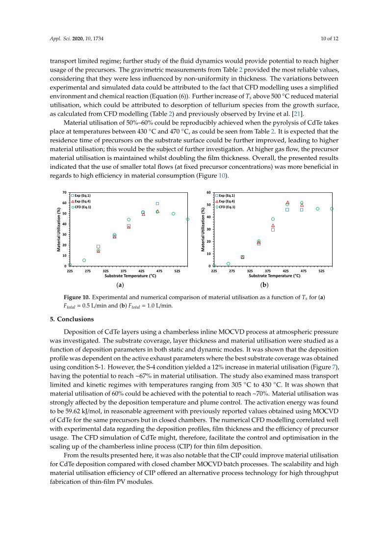
transport limited regime; further study of the fluid dynamics would provide potential to reach higherusage of the precursors. The gravimetric measurements from Table 2 provided the most reliable values,considering that they were less influenced by non-uniformity in thickness. The variations betweenexperimental and simulated data could be attributed to the fact that CFD modelling uses a simplifiedenvironment and chemical reaction (Equation (6)). Further increase of Ts above 500 ◦C reduced materialutilisation, which could be attributed to desorption of tellurium species from the growth surface,as calculated from CFD modelling (Table 2) and previously observed by Irvine et al. [21].
Material utilisation of 50%–60% could be reproducibly achieved when the pyrolysis of CdTe takesplace at temperatures between 430 ◦C and 470 ◦C, as could be seen from Table 2. It is expected that theresidence time of precursors on the substrate surface could be further improved, leading to highermaterial utilisation; this would be the subject of further investigation. At higher gas flow, the precursormaterial utilisation is maintained whilst doubling the film thickness. Overall, the presented resultsindicated that the use of smaller total flows (at fixed precursor concentrations) was more beneficial inregards to high efficiency in material consumption (Figure 10).Appl. Sci. 2020, 10, x FOR PEER REVIEW 10 of 11
Figure 10. Experimental and numerical comparison of material utilisation as a function of Ts for (a)
Ftotal = 0.5 l/min and (b) Ftotal = 1.0 l/min.
5. Conclusions
Deposition of CdTe layers using a chamberless inline MOCVD process at atmospheric pressure
was investigated. The substrate coverage, layer thickness and material utilisation were studied as a
function of deposition parameters in both static and dynamic modes. It was shown that the
deposition profile was dependent on the active exhaust parameters where the best substrate coverage
was obtained using condition S-1. However, the S-4 condition yielded a 12% increase in material
utilisation (Figure 7), having the potential to reach ~67% in material utilisation. The study also
examined mass transport limited and kinetic regimes with temperatures ranging from 305 °C to 430
°C. It was shown that material utilisation of 60% could be achieved with the potential to reach ~70%.
Material utilisation was strongly affected by the deposition temperature and plume control. The
activation energy was found to be 59.62 kJ/mol, in reasonable agreement with previously reported
values obtained using MOCVD of CdTe for the same precursors but in closed chambers. The
numerical CFD modelling correlated well with experimental data regarding the deposition profiles,
film thickness and the efficiency of precursor usage. The CFD simulation of CdTe might, therefore,
facilitate the control and optimisation in the scaling up of the chamberless inline process (CIP) for
thin film deposition.
From the results presented here, it was also notable that the CIP could improve material
utilisation for CdTe deposition compared with closed chamber MOCVD batch processes. The
scalability and high material utilisation efficiency of CIP offered an alternative process technology
for high throughput fabrication of thin-film PV modules.
Author Contributions: Conceptualisation, S.M., V.B. and S.J.C.I.; methodology, G.K.; software, S.M. and X.Y.;
validation, S.M.; formal analysis, G.K., V.B., D.L., S.J.C.I. and X.Y.; investigation, S.M., G.K., V.B., D.L., S.J.C.I.
and X.Y.; writing—original draft preparation, S.M. and Y.V.; writing—review and editing, S.M. and Y.V.;
visualisation, G.K.; supervision, V.B., D.L., S.J.C.I., X.Y. and Y.V. All authors have read and agreed to the
published version of the manuscript.
Funding: This research was funded by the European Regional Development Fund through the Low Carbon
Research Institute Programme (WEFO-80366) for the Solar Photovoltaic Academic Research Consortium
(SPARC) Cymru project and by the European Social Fund project (case ID 80300) for a Knowledge Economy
Skills Scholarship (KESS).
Acknowledgements: The authors would like to thank ESF and MD Ian Owen from Scanwel Ltd. for funding the
Knowledge Economy Skills Scholarship (KESS) and the Low Carbon Research Institute (LCRI) for funding the
SPARC project. Paul Warren, from NSG Pilkington, is also thanked for supplying the TEC glass for the SPARC
project and Design Engineer Steve Truman from Scanwel Ltd. for the design and assembly of the coating heads.
The authors would also like to thank Peter Siderfin and Steve Jones, CSER, for their help in the commissioning
of the SPARC inline deposition system. Damien Jones and Julien Haillet are also acknowledged for their
contributions to the PLC programming on the system.
Conflicts of Interest: The authors declare no conflict of interest.
(a) (b)
0
10
20
30
40
50
60
70
225 275 325 375 425 475 525
Mat
eria
l Uti
lizat
ion
(%
)
Substrate Temperature (°C)
Exp (Eq.1)
Exp (Eq.4)
CFD (Eq.1)
0
10
20
30
40
50
60
225 275 325 375 425 475 525
Mat
eria
l Uti
lizat
ion
(%
)
Substrate Temperature (°C)
Exp (Eq.1)
Exp (Eq.4)
CFD (Eq.1)
Figure 10. Experimental and numerical comparison of material utilisation as a function of Ts for (a)Ftotal = 0.5 L/min and (b) Ftotal = 1.0 L/min.
5. Conclusions
Deposition of CdTe layers using a chamberless inline MOCVD process at atmospheric pressurewas investigated. The substrate coverage, layer thickness and material utilisation were studied as afunction of deposition parameters in both static and dynamic modes. It was shown that the depositionprofile was dependent on the active exhaust parameters where the best substrate coverage was obtainedusing condition S-1. However, the S-4 condition yielded a 12% increase in material utilisation (Figure 7),having the potential to reach ~67% in material utilisation. The study also examined mass transportlimited and kinetic regimes with temperatures ranging from 305 ◦C to 430 ◦C. It was shown thatmaterial utilisation of 60% could be achieved with the potential to reach ~70%. Material utilisation wasstrongly affected by the deposition temperature and plume control. The activation energy was foundto be 59.62 kJ/mol, in reasonable agreement with previously reported values obtained using MOCVDof CdTe for the same precursors but in closed chambers. The numerical CFD modelling correlated wellwith experimental data regarding the deposition profiles, film thickness and the efficiency of precursorusage. The CFD simulation of CdTe might, therefore, facilitate the control and optimisation in thescaling up of the chamberless inline process (CIP) for thin film deposition.
From the results presented here, it was also notable that the CIP could improve material utilisationfor CdTe deposition compared with closed chamber MOCVD batch processes. The scalability and highmaterial utilisation efficiency of CIP offered an alternative process technology for high throughputfabrication of thin-film PV modules.

Appl. Sci. 2020, 10, 1734 11 of 12
Author Contributions: Conceptualisation, S.M., V.B. and S.J.C.I.; methodology, G.K.; software, S.M. and X.Y.;validation, S.M.; formal analysis, G.K., V.B., D.L., S.J.C.I. and X.Y.; investigation, S.M., G.K., V.B., D.L., S.J.C.I. andX.Y.; writing—original draft preparation, S.M. and Y.V.; writing—review and editing, S.M. and Y.V.; visualisation,G.K.; supervision, V.B., D.L., S.J.C.I., X.Y. and Y.V. All authors have read and agreed to the published version ofthe manuscript.
Funding: This research was funded by the European Regional Development Fund through the Low CarbonResearch Institute Programme (WEFO-80366) for the Solar Photovoltaic Academic Research Consortium (SPARC)Cymru project and by the European Social Fund project (case ID 80300) for a Knowledge Economy SkillsScholarship (KESS).
Acknowledgments: The authors would like to thank ESF and MD Ian Owen from Scanwel Ltd. for funding theKnowledge Economy Skills Scholarship (KESS) and the Low Carbon Research Institute (LCRI) for funding theSPARC project. Paul Warren, from NSG Pilkington, is also thanked for supplying the TEC glass for the SPARCproject and Design Engineer Steve Truman from Scanwel Ltd. for the design and assembly of the coating heads.The authors would also like to thank Peter Siderfin and Steve Jones, CSER, for their help in the commissioning ofthe SPARC inline deposition system. Damien Jones and Julien Haillet are also acknowledged for their contributionsto the PLC programming on the system.
Conflicts of Interest: The authors declare no conflict of interest.
References
1. Lee, Y.H.; Chou, K.S.; Lin, M.S. Analysis of the combined effect of mass transfer and decomposition kineticson the growth rates of CdTe by MOCVD. J. Chin. Inst. Eng. 1988, 11, 551–554. [CrossRef]
2. Piotrowski, A.; Madejczyk, P.; Gawron, W.; Klos, K.; Pawluczyk, J.; Grudzien, M.; Piotrowski, J.; Rogalski, A.Growth of MOCVD HgCdTe heterostructures for uncooled infrared photodetectors. Bull. Pol. Acad. Sci.Tech. Sci. 2005, 53, 139–149. [CrossRef]
3. Kartopu, G.; Phillips, L.J.; Barrioz, V.; Irvine, S.J.C.; Hodgson, S.D.; Tejedor, E.; Dupin, D.; Clayton, A.J.;Rugen-Hankey, S.L.; Durose, K. Progression of metalorganic chemical vapour-deposited CdTe thin-film PVdevices towards modules. Prog. Photovolt. Res. Appl. 2016, 24, 283–291. [CrossRef]
4. Luceno-Sanchez, J.A.; Diez-Pascual, A.M.; Capilla, R.P. Materials for photovoltaics: State of art and recentdevelopments. Int. J. Mol. Sci. 2019, 20, 976. [CrossRef] [PubMed]
5. Mullin, J.B.; Irvine, S.J.C.; Ashen, D.J. Organometallic growth of II–VI compounds. J. Cryst. Growth 1981, 55,92–106. [CrossRef]
6. Hicks, R.F. The chemistry of the organometallic vapor-phase epitaxy of mercury cadmium telluride. Proc.IEEE 1992, 80, 1625–1640. [CrossRef]
7. Moon, R.L. MOVPE: Is there any other technology for optoelectronics? J. Cryst. Growth 1997, 170, 1–10.[CrossRef]
8. Rushworth, S. High purity metal-organic precursors for CPV device fabrication. Mater. Matters 2010, 5,94–98.
9. McCandless, B.E.; Sites, J.R. Cadmium telluride solar cells. In Handbook of Photovoltaic Science and Engineering,2nd ed.; Luque, A., Hegedus, S., Eds.; Wiley: Chichester, UK, 2012; pp. 600–642.
10. First Solar Hits Cost Reduction Milestone. Available online: https://www.pv-tech.org/news/has_first_solar_retaken_the_lowest_cost_pv_manufacturer_mantle (accessed on 13 December 2019).
11. Green, M.A.; Hishikawa, Y.; Dunlop, E.D.; Levi, D.H.; Hohl-Ebinger, J.; Yoshita, M.; Ho-Baillie, A.W.Y. Solarcell efficiency tables (Version 53). Prog. Photovolt. Res. Appl. 2019, 27, 3–12. [CrossRef]
12. Barrioz, V.; Kartopu, G.; Irvine, S.J.C.; Monir, S.; Yang, X. Material utilisation when depositing CdTe layers byinline AP-MOCVD. J. Cryst. Growth 2012, 354, 81–85. [CrossRef]
13. Kartopu, G.; Barrioz, V.; Irvine, S.J.C.; Clayton, A.J.; Monir, S.; Lamb, D.A. Inline atmospheric pressuremetalorganic chemical vapour deposition for thin film CdTe solar cells. Thin Solid Film. 2014, 558, 374–377.[CrossRef]
14. Mitrovic, B.; Gurary, A.; Quinn, W. Process conditions optimisation for the maximum deposition rate anduniformity in vertical rotating disc MOCVD reactors based on CFD modelling. J. Cryst. Growth 2007, 303,323–329. [CrossRef]
15. Barrioz, V.; Lamb, D.A.; Monir, S.; Trueman, S.; Kartopu, G.; Owen, I.W.; Irvine, S.J.C.; Yang, X. Injector andMethod. Patent WO2014122484A1, 14 August 2014.

Appl. Sci. 2020, 10, 1734 12 of 12
16. Yang, X.; Wu, Y.; Huang, X.; Barrioz, V.; Kartopu, G.; Monir, S.; Irvine, S.J.C. Numerical simulation of thedeposition process and the epitaxial growth of cadmium telluride thin film in a MOCVD reactor. Comput.Therm. Sci. 2013, 5, 177–188. [CrossRef]
17. Barrioz, V.; Monir, S.; Kartopu, G.; Lamb, D.A.; Brooks, W.; Siderfin, P.; Jones, S.; Clayton, A.J.; Irvine, S.J.C.MOCVD for solar cells, a transition towards a chamberless inline process. J. Cryst. Growth 2015, 414, 223–231.[CrossRef]
18. Capper, P. Properties of Narrow Gap Cadmium-Based Compounds; IEE: London, UK, 1994.19. Fluent Inc. Fluent 6.3 UDF Manual; Fluent Inc.: Lebanon, PA, USA, 2006.20. Mazi, M.; Simka, H.; Jensen, K.F. Simulation of carbon doping of GaAs during MOVPE. J. Cryst. Growth 1992,
124, 483–492.21. Irvine, S.J.C.; Bjaj, J. A study of the growth kinetics of II–VI metalorganic vapour phase epitaxy using in situ
laser reflectometry. J. Cryst. Growth 1994, 145, 78–81. [CrossRef]
© 2020 by the authors. Licensee MDPI, Basel, Switzerland. This article is an open accessarticle distributed under the terms and conditions of the Creative Commons Attribution(CC BY) license (http://creativecommons.org/licenses/by/4.0/).