Embed Size (px)
Citation preview

BROADBAND IMPEDANCE MATCHING OF ANTENNA RADIATORS
by
Vishwanath Iyer
A Dissertation
Submitted to the Faculty
of the
WORCESTER POLYTECHNIC INSTITUTE
in partial fulfillment of the requirements for the
Degree of Doctor of Philosophy
in
Electrical and Computer Engineering
August 2010 Approved: Dr. Sergey N. Makarov (Advisor) ____________________________________________ Dr. Reinhold Ludwig (WPI) ________________________________________________ Dr. William Michalson (WPI) _______________________________________________ Dr. Faranak Nekoogar (LLNL) ______________________________________________

ii
To my wife, Smita

iii
Abstract In the design of any antenna radiator, single or multi-element, a significant amount of
time and resources is spent on impedance matching. There are broadly two approaches to
impedance matching; the first is the distributed impedance matching approach which
leads to modifying the antenna geometry itself by identifying appropriate degrees of
freedom within the structure. The second option is the lumped element approach to
impedance matching. In this approach instead of modifying the antenna geometry a
passive network attempts to equalize the impedance mismatch between the source and the
antenna load.
This thesis introduces a new technique of impedance matching using lumped circuits
(passive, lossless) for electrically small (short) non-resonant dipole/monopole antennas.
A closed form upper-bound on the achievable transducer gain (and therefore the
reflection coefficient) is derived starting with the Bode-Fano criterion. A 5 element
equalizer is proposed which can equalize all dipole/monopole like antennas. Simulation
and experimental results confirm our hypothesis.
The second contribution of this thesis is in the design of broadband, small size, modular
arrays (2, 4, 8 or 16 elements) using the distributed approach to impedance matching. The
design of arrays comprising a small number of elements cannot follow the infinite array
design paradigm. Instead, the central idea is to find a single optimized radiator (unit cell)
which if used to build the 2x1, 4x1, 2x2 arrays, etc. (up to a 4x4 array) will provide at
least the 2:1 bandwidth with a VSWR of 2:1 and stable directive gain (≤ 3 dB variation)
in each configuration. Simulation and experimental results for a solution to the 2x1, 4x1
and 2x2 array configurations is presented.

iv
Acknowledgement This dissertation describes the research work done during my time at the Antenna Lab, in the ECE department at WPI.
I thank Prof. Sergey Makarov for agreeing to be my advisor, for allowing me to observe and learn, for being generous with his time and energy, for having faith in me, for giving me the space to explore, and contribute to a variety of different topics (indeed, only after we had pinned down my thesis topic), and for asking more of me. I also want to thank his wife Natasha for her warmth and kindness.
I thank Prof. Reinhold Ludwig, Prof. William Michalson and Dr. Faranak Nekoogar for agreeing to serve on my thesis committee and providing me with feedback. I was fortunate enough to assist Prof. Ludwig with ECE 2112 and ECE 3113 as a TA. I thoroughly enjoyed my interactions with him and with the students. I also thank him for giving me the opportunity to help out with the course instruction for ECE 2112 and see up close the classroom dynamic from the other side!
I thank Prof. Michalson for entertaining the initial email from me, accepting me as a Ph.D. student, and advising me.
I thank Dr. Nekoogar for interacting with me on several occasions regarding my thesis work and also for giving me the opportunity to collaborate on the book chapter.
My time during the Ph.D. would not have materialized if not for the support from the ECE department for my education in the form of the Teaching Assistantship. I thank Prof. Fred Looft for his continuous support. I would also like to thank Cathy, Colleen, Brenda and Stacie in the ECE office for the assistance, conversations and of course for being the keepers of all things sweet. Many thanks to Bob Brown for his assistance with the all important ECE server cluster.
My friends in the Antenna Lab, Daniel Harty, Brian Janice, Ed Oliveira and Tao Li made this experience richer. Special thanks to Daniel - the big array guy, who helped me with experimentally verifying the lumped component and distributed matching techniques presented in this thesis. A big thank you to Brian – super god balun steiner for his help with the modular array analysis and the simulation of the Dorne-Margolin blade monopole. I have enjoyed each and every crazy conversation we have had over the past 3 years ! Thank you and good luck for everything in the future.
I am glad I pursued the Ph.D. in the company of my friends Abhijit, Hemish, Jitish, and Shashank. Our discussions on everything technological and non-technological will always be cherished by me.

v
I would like to thank my mother, father, and sister for giving me the support and encouragement to pursue my goals. Finally, I want to thank my wife Smita for the sacrifices she has made. Thank you for your immeasurable contributions to this thesis. You are amazing!

vi
Table of Contents Abstract ........................................................................................................................................... iii
Acknowledgement .......................................................................................................................... iv
Table of Contents ............................................................................................................................ vi
List of Figures ................................................................................................................................. ix
List of Tables ................................................................................................................................. xv
Chapter 1. Introduction to impedance matching of antenna radiators ............................................. 1
1.1 Impedance matching – the beginnings ................................................................................... 2
1.2 Impedance matching categories ............................................................................................. 3
1.3 Bode-Fano theory and the analytic approach ......................................................................... 5
1.4 The Real Frequency Technique ............................................................................................. 7
1.5 Wideband matching of antenna radiators ............................................................................... 8
1.5.1 Motivation for wideband matching of an electrically small (short) dipole/monopole using a lumped circuit .............................................................................................................. 9
1.5.2 Motivation for design of modular arrays of resonant antenna radiators and broadband matching using the distributed approach ............................................................................... 11
1.6 Thesis organization .............................................................................................................. 13
Chapter 2. Theoretical limit on wideband impedance matching for a non-resonant dipole/monopole ............................................................................................................................ 14
2.1 The electrically small dipole ................................................................................................ 14
2.2 Analytical solution for the input impedance of a small dipole ............................................ 15
2.3 Antenna impedance model ................................................................................................... 19
2.4 Comparison of impedance model with full wave EM simulation ........................................ 20
2.5 Wideband impedance matching – the reflective equalizer .................................................. 21
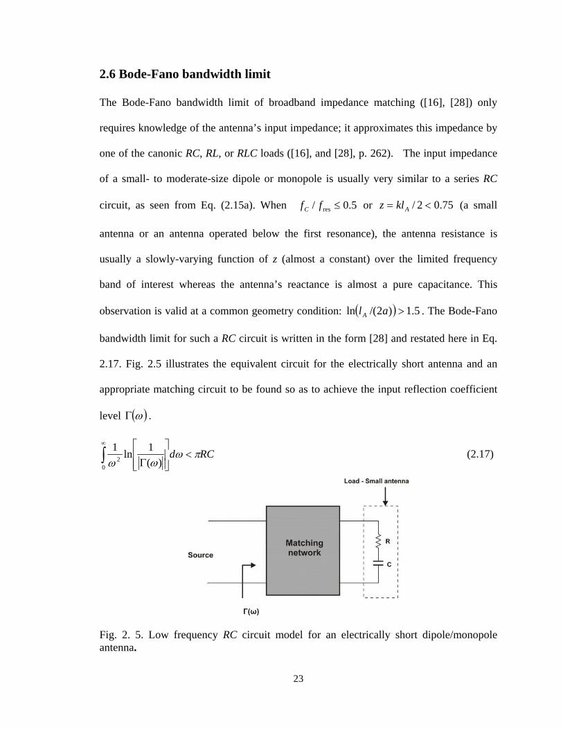
2.6 Bode-Fano bandwidth limit ................................................................................................. 23
2.7 Gain-bandwidth product (small fractional bandwidth, small gain) ..................................... 24
2.8 The arbitrary fractional bandwidth and gain scenario .......................................................... 26
2.9 Dipole vs. monopole ............................................................................................................ 27
2.10 Comparison with Chu's bandwidth limit ............................................................................ 28
Chapter 3. Equalizer circuit development for the non-resonant dipole/monopole like antenna .... 31
3.1 Single and double tuning for the electrically short dipole ................................................... 31
3.2 Analysis of double tuning circuit (L-section) ...................................................................... 33
3.3 Sensitivity of the double tuning circuit ................................................................................ 35
3.4 Analysis of single tuning circuit .......................................................................................... 39
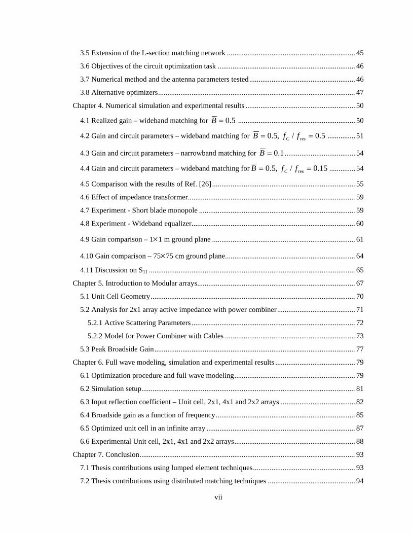
vii
3.5 Extension of the L-section matching network ..................................................................... 45
3.6 Objectives of the circuit optimization task .......................................................................... 46
3.7 Numerical method and the antenna parameters tested ......................................................... 46
3.8 Alternative optimizers .......................................................................................................... 47
Chapter 4. Numerical simulation and experimental results ........................................................... 50
4.1 Realized gain – wideband matching for 5.0=B ............................................................... 50
4.2 Gain and circuit parameters – wideband matching for 5.0/,5.0 res == ffB C ............... 51
4.3 Gain and circuit parameters – narrowband matching for 1.0=B ...................................... 54
4.4 Gain and circuit parameters – wideband matching for 15.0/,5.0 res == ffB C .............. 54
4.5 Comparison with the results of Ref. [26] ............................................................................. 55
4.6 Effect of impedance transformer .......................................................................................... 59
4.7 Experiment - Short blade monopole .................................................................................... 59
4.8 Experiment - Wideband equalizer ........................................................................................ 60
4.9 Gain comparison – 1×1 m ground plane ............................................................................. 61
4.10 Gain comparison – 75×75 cm ground plane ...................................................................... 64
4.11 Discussion on S11 ............................................................................................................... 65
Chapter 5. Introduction to Modular arrays ..................................................................................... 67
5.1 Unit Cell Geometry .............................................................................................................. 70
5.2 Analysis for 2x1 array active impedance with power combiner .......................................... 71
5.2.1 Active Scattering Parameters ........................................................................................ 72
5.2.2 Model for Power Combiner with Cables ...................................................................... 73
5.3 Peak Broadside Gain ............................................................................................................ 77
Chapter 6. Full wave modeling, simulation and experimental results ........................................... 79
6.1 Optimization procedure and full wave modeling ................................................................. 79
6.2 Simulation setup ................................................................................................................... 81
6.3 Input reflection coefficient – Unit cell, 2x1, 4x1 and 2x2 arrays ........................................ 82
6.4 Broadside gain as a function of frequency ........................................................................... 85
6.5 Optimized unit cell in an infinite array ................................................................................ 87
6.6 Experimental Unit cell, 2x1, 4x1 and 2x2 arrays ................................................................. 88
Chapter 7. Conclusion .................................................................................................................... 93
7.1 Thesis contributions using lumped element techniques ....................................................... 93
7.2 Thesis contributions using distributed matching techniques ............................................... 94

viii
7.3 Future research directions .................................................................................................... 95
Appendix A – Impedance Matching of Small Dipole and Loop Antennas for Wideband RFID Operation ....................................................................................................................................... 97
Appendix B – ADS analysis of a monopole with reflective equalizer ....................................... 110
Appendix C – Comparison of input impedance of the electrically small dipole and loop antennas using analytical, Method of Moments (MoM) and Ansoft HFSS solutions ................................ 113
Appendix D – Example design of single and dual band matching networks ............................... 121
Appendix E – Upper Limit on System Efficiency for Electrically Small Dipole and Loop Antennas with Matching Networks.............................................................................................. 127
Appendix F – Reflectionless equalizers for an electrically small monopole and a dielectrically (truncated hemisphere) loaded top-hat monopole antenna .......................................................... 135
Appendix G – Code ..................................................................................................................... 146
References .................................................................................................................................... 178
ix
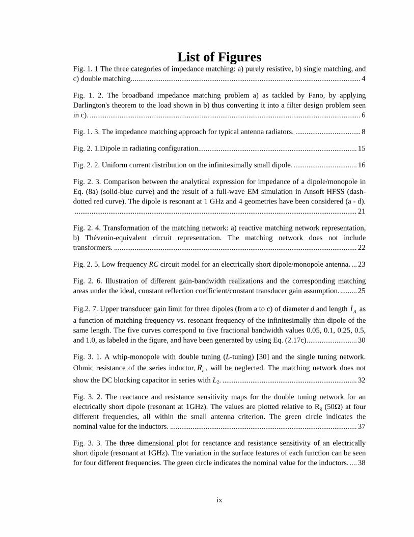
List of Figures Fig. 1. 1 The three categories of impedance matching: a) purely resistive, b) single matching, and c) double matching. .......................................................................................................................... 4
Fig. 1. 2. The broadband impedance matching problem a) as tackled by Fano, by applying Darlington's theorem to the load shown in b) thus converting it into a filter design problem seen in c). ................................................................................................................................................. 6
Fig. 1. 3. The impedance matching approach for typical antenna radiators. ................................... 8
Fig. 2. 1.Dipole in radiating configuration. .................................................................................... 15
Fig. 2. 2. Uniform current distribution on the infinitesimally small dipole. .................................. 16
Fig. 2. 3. Comparison between the analytical expression for impedance of a dipole/monopole in Eq. (8a) (solid-blue curve) and the result of a full-wave EM simulation in Ansoft HFSS (dash-dotted red curve). The dipole is resonant at 1 GHz and 4 geometries have been considered (a - d).
....................................................................................................................................................... 21
Fig. 2. 4. Transformation of the matching network: a) reactive matching network representation, b) Thévenin-equivalent circuit representation. The matching network does not include transformers. .................................................................................................................................. 22
Fig. 2. 5. Low frequency RC circuit model for an electrically short dipole/monopole antenna. ... 23
Fig. 2. 6. Illustration of different gain-bandwidth realizations and the corresponding matching areas under the ideal, constant reflection coefficient/constant transducer gain assumption. ......... 25
Fig.2. 7. Upper transducer gain limit for three dipoles (from a to c) of diameter d and length Al as a function of matching frequency vs. resonant frequency of the infinitesimally thin dipole of the same length. The five curves correspond to five fractional bandwidth values 0.05, 0.1, 0.25, 0.5, and 1.0, as labeled in the figure, and have been generated by using Eq. (2.17c). .......................... 30
Fig. 3. 1. A whip-monopole with double tuning (L-tuning) [30] and the single tuning network. Ohmic resistance of the series inductor, oR , will be neglected. The matching network does not
show the DC blocking capacitor in series with L2. ........................................................................ 32
Fig. 3. 2. The reactance and resistance sensitivity maps for the double tuning network for an electrically short dipole (resonant at 1GHz). The values are plotted relative to Rg (50Ω) at four different frequencies, all within the small antenna criterion. The green circle indicates the nominal value for the inductors. .................................................................................................... 37
Fig. 3. 3. The three dimensional plot for reactance and resistance sensitivity of an electrically short dipole (resonant at 1GHz). The variation in the surface features of each function can be seen for four different frequencies. The green circle indicates the nominal value for the inductors. .... 38
x
Fig. 3. 4. The reactance and resistance sensitivity maps for the double tuning network for an electrically short dipole (resonant at 1GHz). The values are plotted relative to four different values of Rg at fC = 100 MHz. The green circle indicates the nominal value for the inductors. .... 41
Fig. 3. 5. The three dimensional plot for reactance and resistance sensitivity of an electrically short dipole (resonant at 1GHz). The surface features of each function can be seen for four different values of generator resistance. The green circle indicates the nominal value for the inductors. ........................................................................................................................................ 42
Fig. 3. 6. The reactance and resistance sensitivity maps for the double tuning network for an electrically short dipole (resonant at 1GHz). The values are plotted relative to four different values of 60=dlA at fC = 0.5 GHz. The green circle indicates the nominal value for the inductors. ........................................................................................................................................ 43
Fig. 3. 7. The three dimensional plot for reactance and resistance sensitivity of an electrically short dipole (resonant at 1GHz). The surface features of each function can be seen for four different values of generator resistance. The green circle indicates the nominal value for the inductors. ........................................................................................................................................ 44
Fig. 3. 8. An extension of the L-tuning network for certain fixed values of 21 , LL by the T-match. ....................................................................................................................................................... 45
Fig. 4. 1. Realized average generator gain T over the band (circles) based on the ±25% gain variation rule at different matching center frequencies and 5.0=B for three different dipoles, obtained through numerical simulation. The realized values are shown by circles; the ideal upper estimates of 0T from Fig. 2.7 are given by solid curves, which are realized by using eqn. (2.22c).
....................................................................................................................................................... 53
Fig. 4. 2. Gain variation with frequency for a short dipole or for an equivalent monopole at different thicknesses/widths obtained by numerical simulation which uses Eq. (2.16). Matching is done for 5.0/ res =ffC , 5.0≈B based on the ±25% gain variation rule. Vertical lines show the
center frequency and the passband. ............................................................................................... 56
Fig. 4. 3. Gain variation with frequency for a short dipole or for an equivalent monopole at different thicknesses/widths obtained by numerical simulation which uses Eq. (2.16). Matching is done for 15.0/ res =ffC , 5.0≈B based on the ±25% gain variation rule. Vertical lines show
the center frequency and the passband. .......................................................................................... 57
Fig. 4. 4. Gain variation with frequency for a short dipole or for an equivalent monopole of length 0.5 m and radius of 0.001m, by numerical simulation of associated matching network. Matching is done for 416.0/ res =ffC , 4.0=B based on the ±25% gain variation rule (dashed curve).
The thick solid curve is the result of Ref. [25] with the modified Carlin’s equalizer, which was optimized over the same passband for the same dipole. Vertical lines show the center frequency
xi
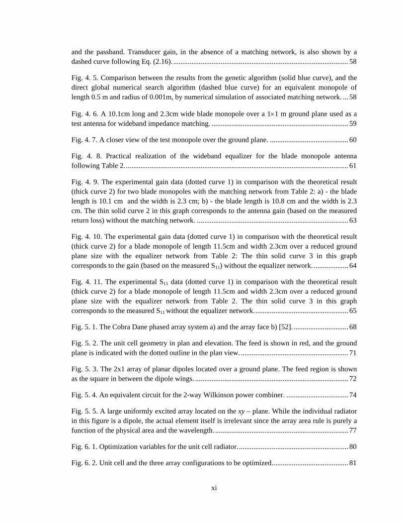
and the passband. Transducer gain, in the absence of a matching network, is also shown by a dashed curve following Eq. (2.16). ................................................................................................ 58
Fig. 4. 5. Comparison between the results from the genetic algorithm (solid blue curve), and the direct global numerical search algorithm (dashed blue curve) for an equivalent monopole of length 0.5 m and radius of 0.001m, by numerical simulation of associated matching network. ... 58
Fig. 4. 6. A 10.1cm long and 2.3cm wide blade monopole over a 1×1 m ground plane used as a test antenna for wideband impedance matching. ........................................................................... 59
Fig. 4. 7. A closer view of the test monopole over the ground plane. ........................................... 60
Fig. 4. 8. Practical realization of the wideband equalizer for the blade monopole antenna following Table 2. .......................................................................................................................... 61
Fig. 4. 9. The experimental gain data (dotted curve 1) in comparison with the theoretical result (thick curve 2) for two blade monopoles with the matching network from Table 2: a) - the blade length is 10.1 cm and the width is 2.3 cm; b) - the blade length is 10.8 cm and the width is 2.3 cm. The thin solid curve 2 in this graph corresponds to the antenna gain (based on the measured return loss) without the matching network. ................................................................................... 63
Fig. 4. 10. The experimental gain data (dotted curve 1) in comparison with the theoretical result (thick curve 2) for a blade monopole of length 11.5cm and width 2.3cm over a reduced ground plane size with the equalizer network from Table 2: The thin solid curve 3 in this graph corresponds to the gain (based on the measured S11) without the equalizer network. ................... 64
Fig. 4. 11. The experimental S11 data (dotted curve 1) in comparison with the theoretical result (thick curve 2) for a blade monopole of length 11.5cm and width 2.3cm over a reduced ground plane size with the equalizer network from Table 2. The thin solid curve 3 in this graph corresponds to the measured S11 without the equalizer network. ................................................... 65
Fig. 5. 1. The Cobra Dane phased array system a) and the array face b) [52]. .............................. 68
Fig. 5. 2. The unit cell geometry in plan and elevation. The feed is shown in red, and the ground plane is indicated with the dotted outline in the plan view. ........................................................... 71
Fig. 5. 3. The 2x1 array of planar dipoles located over a ground plane. The feed region is shown as the square in between the dipole wings. .................................................................................... 72
Fig. 5. 4. An equivalent circuit for the 2-way Wilkinson power combiner. .................................. 74
Fig. 5. 5. A large uniformly excited array located on the xy – plane. While the individual radiator in this figure is a dipole, the actual element itself is irrelevant since the array area rule is purely a function of the physical area and the wavelength. ......................................................................... 77
Fig. 6. 1. Optimization variables for the unit cell radiator. ............................................................ 80
Fig. 6. 2. Unit cell and the three array configurations to be optimized. ......................................... 81

xii
Fig. 6. 3. Optimized unit cell dimensions obtained through full-wave modeling in Ansoft HFSS ver 12.0. ......................................................................................................................................... 82
Fig. 6. 4. The input reflection coefficient for the optimized modular array unit cell. The solid green vertical lines indicate the bandwidth of interest. .................................................................. 83
Fig. 6. 5. The active input reflection coefficient obtained from the simulation of 2x1, 4x1 and 2x2 arrays. The solid green vertical lines indicate the bandwidth of interest ....................................... 84
Fig. 6. 6. The peak directive gain at broadside plotted as a function of frequency for the a) 2x1 array, b) 4x1 array and c) 2x2 arrays. The theoretical estimate (solid curve) is compared with the simulation results (dotted red curve) over the bandwidth of interest (solid green vertical lines). . 86
Fig. 6. 7. The active reflection coefficient for an infinite array using the optimized modular array unit cell as the active element. The solid green vertical lines indicate the bandwidth of interest. . 87
Fig. 6. 8. The three experimental modular arrays. ......................................................................... 89
Fig. 6. 9. The input reflection coefficient for the experimental unit cell radiator. The solid green vertical lines indicate the bandwidth of interest. ............................................................................ 89
Fig. 6. 10. The active input reflection coefficient obtained from the experimental 2x1, 4x1 and 2x2 arrays. The solid green vertical lines indicate the bandwidth of interest. ............................... 91
Fig. 6. 11. H-plane radiation pattern for 2 x 2 modular array at 1 GHz. The solid blue curve is the simulation result from HFSS, while the dashed blue curve is the experimental result. ................. 92
Fig. A. 1. Matching network: a) reactive matching network representation. b) Thévenin-equivalent circuit. ......................................................................................................................... 100
Fig. A. 2. Extension of the L-tuning network for certain fixed values of L1, L2 by the T- section for small dipole. ........................................................................................................................... 102
Fig. A. 3. Extension of the L-tuning network for certain fixed values of C1, C2 by a high pass section for small loop. .................................................................................................................. 103
Fig. A. 4. Realized average generator gain ( )dpT0 (squares) for a small dipole with lA/d=10. ....... 107
Fig. A. 5. Realized average generator gain ( )lpT0 (squares) for a loop with ρ=10. ....................... 107
Fig. A. 6. Upper bound on system efficiency for the small dipole with lA/d=10. ........................ 108
Fig. A. 7. Upper bound on system efficiency for the small loop with ρ=10 ................................ 108
Fig. B. 1. ADS simulation set up. ................................................................................................ 110
Fig. B. 2. ADS simulation set up of the wideband reflective equalizer. ...................................... 111
Fig. B. 3. Simulation result, for L1 = 56nH, C5 = 7.63pF. .......................................................... 112

xiii
Fig. D. 1. Handset model in ANSOFT- HFSS. ............................................................................ 122
Fig. D. 2. Input impedance of blade-handset antenna. ................................................................. 122
Fig. D. 3. Directivity of the blade-handset antenna. .................................................................... 123
Fig. D. 4. Extension of the L-tuning section for fixed values of L1, L2 by the T-section. ........... 124
Fig. D. 5. Average transducer gain. ............................................................................................. 125
Fig. D. 6. S11 of blade-handset antenna without matching network. ............................................ 125
Fig.E. 1. Reactive matching network representation ................................................................... 127
Fig.E. 2. L - Section matching network. ...................................................................................... 128
Fig.E. 3. Upper bound on achievable system efficiency for small dipole. .................................. 130
Fig. E. 5. The achievable system efficiency for an electrically small loop. ................................. 132
Fig. E. 6. The achievable system efficiency for small loop using approximation on radius ....... 133
Fig. E. 7. The dipole quality factor as a function of center frequency of operation. ................... 134
Fig. E. 8. The loop quality factor as a function of center frequency of operation. ...................... 134
Fig. F. 1. A DR antenna in the form of a spherical sector (height - 150mm; width - 458mm) with a metal hat. ................................................................................................................................... 135
Fig. F. 2. The radiation pattern of the dielectrically loaded (truncated hemisphere) top-hat monopole antenna at 110 MHz. Note, that mismatch loss is not taken into account. .................. 136
Fig. F. 3. Input impedance of the spherical-sector antenna. The resonance is observed at 50 MHz. ..................................................................................................................................................... 137
Fig. F. 4. Comparison between the extracted and exact antenna parameters - see Table F.1. ..... 140
Fig. F. 5. The blade monopole from [88]. .................................................................................... 141
Fig. F. 6. Radiation pattern of the blade monopole at 110 MHz. ................................................. 141
Fig. F. 7. Antenna matching: the impedance-matching network and a step-up transformer. ...... 142
Fig. F.8. Transformation of the matching network: a) lossy matching network representation, b) Thévenin-equivalent circuit representation. The matching network does not include transformers.
..................................................................................................................................................... 143
Fig. F. 9. Comparison of the impedance data from simulation and the extracted LCR model for the blade monopole. ..................................................................................................................... 144

xiv
Fig. F. 10. VSWR at the input to the reflection less equalizer and transducer gain for the blade monopole antenna. ....................................................................................................................... 145

xv
List of Tables Table 4. 1. Circuit parameters and gain tolerance for a short dipole with the total length =23 cm. Matching is done for , based on the ±25% gain variation rule. .................................................. 52
Table 4. 2. Practical component values used in the monopole equalizer for dlA / =20 and t = 2.3 cm................................................................................................................................................... 61
Table A. 1. Simulation Parameters .............................................................................................. 105
Table C. 1. Input resistance of a small dipole antenna (Ω ), 30=tl . ....................................... 113
Table C. 2. Input resistance of a small dipole antenna (Ω ), 10=tl ......................................... 114
Table C. 3. Input reactance of a small dipole antenna (Ω ), 30=tl . ....................................... 115
Table C. 4. Input reactance of a small dipole antenna (Ω ), l/t = 10. .......................................... 116
Table C. 5. Input resistance of a small loop antenna (Ω ) 30=tC . .......................................... 117
Table C. 6. Input resistance of a small loop antenna (Ω ) 10=tC . .......................................... 118
Table C. 7. Input reactance of a small loop antenna (Ω ) 30=tC . .......................................... 119
Table C. 8. Input reactance of a small loop antenna (Ω ) 10=tC . ........................................... 120
Table D. 1. Circuit parameters for the matching network used to match the blade-handset antenna to resistive 50Ω source. ................................................................................................................ 124
Table D. 2. Component values for a 5 element reflective equalizer in two different bands along with the average theoretical transducer gain. ............................................................................... 126
Table E. 1. Simulation Parameters. .............................................................................................. 130
Table E. 2. Simulation Parameters. .............................................................................................. 132
Table E. 2. Simulation parameters ............................................................................................... 131
Table E. 3. Simulation Parameters. .............................................................................................. 132
Table E. 4. Simulation Parameters. .............................................................................................. 133
Table F. 1. Model parameters of the input impedance. ................................................................ 140

xvi

1
Chapter 1. Introduction to impedance matching of antenna radiators
The Maxwell equations are truly the foundation on which much of mankind’s
technological prowess rests on. The unification of electricity and magnetism, two very
mysterious forces of nature in the late 1800’s, achieved by James Clerk Maxwell, has
withstood the significant revisions in our understanding of the universe. The invariance
of his equations to General relativity put Maxwell’s theory on a firm pedestal and being a
part of one of the four fundamental forces of nature along with its unification to quantum
mechanics has ensured its timelessness.
The original Maxwell equations were in a very different format than how we recognize it
today. They were 20 equations in total and were written with the help of ‘quaternions’, a
four dimensional number system much like vectors. These twenty equations were recast
into the four popular equations by Oliver Heaviside and Gibbs. In doing so, the
quaternion representation was done away with and in its place the vector notation was
instituted. This modification gave a far more intuitive appeal to the equations and helped
the world of electrical engineering to develop and exploit it to its full potential. While it
is true that to Maxwell goes the credit for unifying electricity and magnetism, we would
be remiss in not stating that his theory rests on the work of such giants as Carl Friedrich
Gauss, André Marie Ampère, and Michael Faraday.
It was Heinrich Hertz, Nikola Tesla, J. C. Bose, Alexander Popov, Thomas Edison and
others who provided the physical manifestation for these mathematical entities. The twin
pillars of electric power and communications (both wired and wireless) on which much

2
of mankind’s current condition rests on, owes itself to the foundations laid down by these
early pioneers. A common requirement for both is the need to ensure an efficient transfer
of power from a source to a load. This can be succinctly stated as impedance matching. If
the load and the source are purely resistive we can relate this to the maximum power
transfer theorem and the need to keep the load resistance the same as the source
resistance. In the case when there are reactive elements present in the circuit, the
condition for maximum power transfer occurs with the use of conjugate impedance
matching. We will delve into this topic in more detail in chapter 2 and 3.
1.1 Impedance matching – the beginnings
The period between 1890 and 1920 was a very significant one for experimental electrical
engineering. It is during this fruitful period that the means for generating, delivering and
using DC (Direct Current) power and AC (Alternating Current) power were invented. In
addition the wireless revolution sweeping across the globe today has its technological
underpinnings also situated during this period. While it is debatable as to the extent to
which impedance matching was used in electric power, wired and wireless
communications applications during this era, it undoubtedly spurred the theoretical
investigations that soon followed.
In [1]-[6] some of the fundamental concepts in electric network theory were presented
and explained. There was a great deal of interest in techniques that could extract a circuit
topology if provided with the required transfer function and the driving point impedance
functions. The invention of the vacuum tube in the early 1900’s and its subsequent
maturity by the 1920’s resulted in a lot of interest in RF power amplifiers. Expectedly,
the impedance matching problem had also to be dealt with. An example of T and П

3
circuits being employed at the output stage of an RF power amplifier is shown in [7]. The
author suggests their use and also discusses in detail the utility of such circuits to couple
the power from the output of the power amplifier to an antenna. Note that the load and
source are both assumed to be resistive. Some of these concepts such as in [1] have
undergone a great deal of scrutiny as seen by the work done by Papoulis [8] from a
purely mathematical perspective, and more recently by Geyi et. al. and Best [9], [10] for
specifically the antenna impedance.
Since the design of filters was relatively well understood, it was but natural for using the
body of work devoted to their design, in order to design impedance matching networks
[11], [12]. Particularly, [12] has a good review of some basic lumped element filter
building blocks and then proceeds to outline two applications which involve impedance
matching inspired from the basic low-pass filter half-sections; one of these is an
impedance matching problem between an RF transmission line and an antenna while the
second one is for building coupling units between video amplifiers.
1.2 Impedance matching categories
In general impedance matching between an arbitrary pair of source and load can be
classified into three categories. These are shown in Fig. 1.1 and outlined below:
a) The resistive matching problem – source and load are both resistive and unequal
b) The single matching problem – source is resistive and the load is complex
c) The double matching problem – source and load are both complex
4
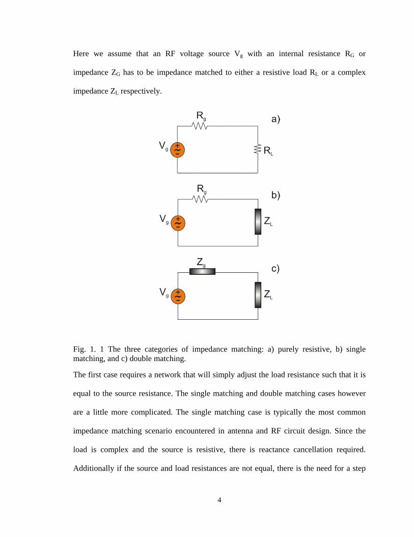
Here we assume that an RF voltage source Vg with an internal resistance RG or
impedance ZG has to be impedance matched to either a resistive load RL or a complex
impedance ZL respectively.
Fig. 1. 1 The three categories of impedance matching: a) purely resistive, b) single matching, and c) double matching.
The first case requires a network that will simply adjust the load resistance such that it is
equal to the source resistance. The single matching and double matching cases however
are a little more complicated. The single matching case is typically the most common
impedance matching scenario encountered in antenna and RF circuit design. Since the
load is complex and the source is resistive, there is reactance cancellation required.
Additionally if the source and load resistances are not equal, there is the need for a step

5
up or step down network to maximize the power transfer (assuming narrowband single
frequency). The double matching case could arise in an RFID (Radio Frequency
IDentification) application where the tag has a chip connected to an antenna. The output
impedance of the chip is usually complex. Ideally, the tag antenna if resonant should have
purely resistive feed point impedance. However, such antennas are sensitive to their
environment and can easily be detuned thus resulting in complex impedance being
presented to the chip’s input. A non-resonant antenna might be a better solution in this
case since it would get rid of the antenna’s sensitivity to its surrounding environment and
we would still end up with a double matching problem.
1.3 Bode-Fano theory and the analytic approach
The first steps towards a theoretical basis for broadband matching were taken by Bode
[13]. While this work considered a simple load (parallel combination of resistor and
capacitor) under the single matching category, it was significant because for the first time
engineers had a bound, cast in a gain-bandwidth formulation, for a given load. Central to
Bode's work is the analytical approach which requires a circuit approximation of the load
impedance as it uses the data in the complex frequency plane; it has been developed for
simple load circuits only. This approach, unlike [7], [11], [14], and [15], did not provide
the techniques to build a good impedance matching network. It did however give the
designer a mathematical tool to compare the performance of a designed impedance
matching network with a specified bandwidth in terms of the gain or the reflection
coefficient. This approach was further investigated by Fano [16] and Youla [17].

6
Of particular importance is the utilization of Darlington's powerful theorem [6] (Sidney
Darlington is arguable more famous for the transistor configuration ‘Darlington pair’) by
Fano together with the work done earlier by Bode, to convert the broadband impedance
matching problem into a filter design problem. This theorem states that any physically
realizable impedance function can be decomposed into a purely reactive lossless network
terminated into a 1Ω resistor (done so by including a transformer in to the reactive
network). Since the source resistance can also be changed to 1Ω by including a
transformer, the impedance matching problem gets converted to a filter design problem.
As shown in Fig. 1. 2, this is a partial filter design problem pertaining to the design of the
first network, since the second network is already discovered through application of
Darlington's theorem.
Fig. 1. 2. The broadband impedance matching problem a) as tackled by Fano, by applying Darlington's theorem to the load shown in b) thus converting it into a filter design problem seen in c).

7
As filter design was a mature art by this period, it was a tremendous boost to this nascent
field of broadband impedance matching. Later, Chen and co-authors implemented
Youla’s theory for LCR loads of the type (C||R) +L [18], [19], and [20]. Of special note is
Ref. [21], where a band-pass Chebyshev equalizer was presented for a Darlington type-C
load, i.e. for R1 + C||R2. This load can reference the input impedance of a small dipole or
monopole. Also to be noted are the Takahasi design formulas for wideband bandpass
Chebyshev ladder networks, which are matching series and parallel LCR loads, see Ref.
[22]. This method bypasses the gain – bandwidth theory and directly produces lumped
lossless equalizers.
1.4 The Real Frequency Technique
The progress in analytic approaches to broadband impedance matching was tempered by
the fact that designers needed to approximate the load with a circuit model. As noted in
section 1.3 the analytic techniques work well for simple load types. However, for more
complicated loads the analytic approach is too difficult. The Carlin’s Real Frequency
Technique (RFT) based gain-bandwidth optimization approach [22]-[25] is a numerical
technique that does not require any circuit approximation of the load impedance. Instead,
it relies on the actual measurement data of the load. A comprehensive review has been
recently provided by Newman [26]. Although being quite versatile, this approach, along
with the pure optimization step, still requires non-unique operations with rational
polynomial approximations, and further extraction of equalizer parameters using the
Darlington procedure [26]. Moreover, a transformer is required to match the obtained
equalizer to the fixed generator resistance of 50Ω [26].

8
1.5 Wideband matching of antenna radiators
For modern wideband or multiband hand-held radios typically used in either civilian or
military roles, it is often desired to match a non-resonant (i.e., relatively short) monopole,
or dipole-like, antenna over a wide frequency band. Current impedance matching
techniques involve modifying the antenna structure and are in fact quite popular. Fig. 1.3
captures the state of the art in impedance matching (narrowband and wideband) for
antennas.
Fig. 1. 3. The impedance matching approach for typical antenna radiators.
Both approaches to impedance matching can be implemented either by including loss
within the structure/network, or by a completely lossless approach. In the distributed
approach to impedance matching, loss can be included, either intentionally or by
circumstance, through the use of dielectric materials. The lumped element approach to
lossy matching involves the inclusion of a properly chosen resistance located strategically
within the network of inductors and capacitors. This is to be differentiated from the

9
lossless matching networks which are designed only with inductors and capacitors.
Naturally, these components have a finite Q (Quality factor) and therefore some degree of
loss does exist even in otherwise lossless networks.
This thesis makes contributions to both the lumped element and distributed approaches to
impedance matching for antenna radiators. Two interesting and challenging problems
have been considered; namely, the broadband impedance matching for electrically small
(short) non-resonant dipoles/monopoles and the design of small sized resonant antenna
arrays of a modular architecture. The problem of wideband matching for short non-
resonant dipoles/monopoles is tackled using lumped element lossless equalizers. In
addition we also provide insight into a lossy matching approach using lumped element
circuits, for a blade monopole and compare it to the performance of a novel dielectrically
loaded (truncated hemisphere) top-hat monopole antenna. The broadband modular array
design focuses on a distributed approach to impedance matching.
1.5.1 Motivation for wideband matching of an electrically small (short)
dipole/monopole using a lumped circuit
Our motivation for pursuing this goal is three-fold, namely:
I. For electrically small, non-resonant antennas distributed impedance matching
techniques that involve modifying the antenna structure, together with
optimization carried out within a full-wave electromagnetic simulation
environment, are sometimes complicated to design, build, and analyze. The
approach suggested in this thesis would minimize the complexity in wideband
matching of short, non-resonant antennas.

10
II. Resonant antennas are extremely sensitive to their surroundings. For hand held
radios, smart phones etc., the antenna is usually electrically small (short) and is
indeed resonant. These antennas are exposed to different materials such as the
human body, wood, metal, liquids etc. on a regular basis and as a result, they get
detuned regularly. To compensate for this, the designer must take into account the
different conditions that maybe most often encountered by the antenna for the
specified application and model these within the full wave EM simulator.
Depending on the kind of objects that might be modeled, the simulation
complexity increases. It may be a better alternative in to deploy a non-resonant
antenna with the kind of matching network suggested in this thesis.
III. This approach could also serve as a basis for building adaptive matching networks
that modify the antenna response dynamically.
The standard narrowband impedance matching techniques include L ,T , and Π sections
of reactive lumped circuit elements, which may also include transformers with single-
and double-stub tuning of transmission lines [27], [28]. The ever growing trend of
miniaturization of wireless devices ensures that size remains an important constraint to
satisfy. In the VHF-UHF bands, where there is a high concentration of wireless services,
lumped circuits are preferable as they have a smaller size. However, the narrowband
matching circuits are usually non-applicable when the bandwidth is equal to 20% or
higher.
The notion of wideband antenna matching to a generator with a fixed generator resistance
of 50Ω is a classical impedance matching concept. As discussed earlier in sections 1.3
and 1.4 respectively as well as in Ref. [29] in general, wideband matching circuit design

11
methods can be classified into two groups: the analytical approach and the Real
Frequency Technique (RFT) numerical approach. When the load is such a well-known
subject as a short dipole or monopole, we can capitalize on prior experience with its
impedance matching, and thus considerably simplify the problem.
This thesis studies the wideband matching problem for short dipoles or monopoles and
does not use the two approaches discussed above. Instead, we prefer to introduce the
equalizer topology up front: the equalizer’s first section is the L section with two
inductors. This section is adopted from the analysis of whip monopoles. Its double-tuning
version has shown excellent performance for impedance matching and tuning of a whip
monopole antenna over a wide band of frequencies [30]. The second and last section is a
high-pass T-section with a shunt inductor and two capacitors. This section is intended to
broaden the narrowband response of the L-section. The equalizer has only five lumped
elements: three inductors and two capacitors. A direct numerical optimization technique
is then employed to find the circuit parameters for wideband impedance matching. Here,
the antenna impedance is approximated by an accurate analytical expression [31]. This
matching network topology can be used for all dipole-like antennas. We will show that
the present simple circuit yields an average band gain that is virtually identical to the gain
obtained with an improved Carlin’s equalizer [26]. This result is shown to be valid for a
wide range of antenna lengths and radii (or widths for a blade dipole/monopole).
1.5.2 Motivation for design of modular arrays of resonant antenna
radiators and broadband matching using the distributed approach
This thesis proposes a new approach to the design of small size wideband arrays of planar
dipoles situated over a ground plane. The individual radiator which we refer to as the unit
12
cell, is resonant. The unit cell terminology is also commonly used for the individual
radiator within large size finite arrays, and therefore not to be confused with it.
Incidentally the design of those large arrays follows the Floquet theoretic infinite array
simulation methodology which we propose and show to be inapplicable for the design of
small size modular arrays. The motivation for pursuing this problem is three-fold:
I. There is much interest in the design of small size arrays in either linear or planar
configurations in the wireless industry. This can be seen with the advent of
MIMO (Multiple Input Multiple Output) systems for 4G, digital TV reception and
also wireless positioning.
II. A modular architecture as proposed in this thesis could be a good solution as it is
inherently flexible. Particularly, it is very easy to change the array configuration
from a 2x2 to a 4x1 (planar to linear).
III. The key aspect of this approach is that a single optimized unit cell could be used
in different configurations without degrading the performance objectives.
The modular design results in increased impedance bandwidth ( 1:2≥ ), as well as higher
directive gain at the low frequencies. We also seek a maximum gain variation over the
band of up to 3dB. Furthermore, we show that the careful design of the individual
radiator may achieve such high bandwidths for the 2x1 array, 2x2 array, and 4x1 array of
the same radiators respectively. The dipole and ground plane within each unit cell can be
mounted on a thin, low epsilon and low loss dielectric material such as Poly methyl
methacrylate (PMMA), commonly known as Plexiglass or on PVC (Polyvinyl Chloride).
An analytical model for the power combiner is introduced and used during optimization
of the arrays. Such a modular approach is well suited for low-cost large-volume small

13
broadside array design. The arrays presented here are intended for use in the UHF region
of the spectrum but can be easily scaled and optimized for other bands.
1.6 Thesis organization
The thesis is organized as follows:
In chapter 2 the theoretical limit to wideband matching of an electrically small (short)
non-resonant dipole/monopole is introduced. The matching circuit for such antennas is
developed in chapter 3. In chapter 4 the simulation results and the experimental results
are provided along with a discussion on the performance. Large portions of the content in
chapters 2- 4 have been drawn from [70]. The modular array concept is introduced in
chapter 5 along with the design approach. A model for the power combiner is also
introduced. In chapter 6 simulation and experimental results are presented. Chapter 7
concludes the thesis and includes suggestions for future research efforts.

14
Chapter 2. Theoretical limit on wideband impedance matching for a non-resonant dipole/monopole
To understand the limitations on wideband impedance matching for a non-resonant
dipole/monopole, it is important to first grasp its impedance behavior. The impedance
behavior is the variation of the resistance, denoted as R and the reactance, denoted as X,
with frequency. The impedance behavior is directly linked (as to be expected) with the
current and voltage standing waves that are setup over the physical extent of the antenna,
in this case the dipole/monopole. In this chapter, we attack this question of the impedance
behavior initially from first principles by using Maxwell's equations, and subsequently by
the use of a semi-empirical analytical expression. Confirmation between the analytical
formulation and a full wave EM (Electromagnetic) simulation is also provided. The
necessary conditions upon which the model depends on will be established. The
reflective equalizer will be introduced and the analysis using Bode-Fano theory will be
described. To understand the effect of geometry three different cases of the dipole will be
considered for wideband matching. Last, but not the least, an introduction to the Chu
limit and a discussion on the results within this context is provided.
2.1 The electrically small dipole
We will begin our discussion on dipoles with the small dipole. The small dipole is also
referred to in literature as the electrically small dipole. This definition implies that the
length of the dipole is much smaller than the wavelength at which it operates. While this
definition is qualitatively satisfying, a quantitative justification is however required
15
regarding what constitutes the electrically small limit. There is much to be said in this
regard. We will defer this discussion for now and simply state that for the purpose of the
next few sections our definition of electrically small assumes that the length of the dipole,
denoted as λ<<Al , where λ is the free space wavelength of operation.
A fundamental quantity of interest for any antenna is its input impedance. The input
impedance allows us to view the antenna from a circuit theoretic perspective and
therefore give us all the well developed circuit analysis techniques to analyze it with.
Once the input impedance is derived, we can replace the antenna with an equivalent
circuit representative of the impedance (at least for the small antenna case) and derive
useful parameters such as reflection coefficient (return loss), efficiency, gain etc. To
begin the analysis however, we will start with the Maxwell’s equations.
2.2 Analytical solution for the input impedance of a small dipole
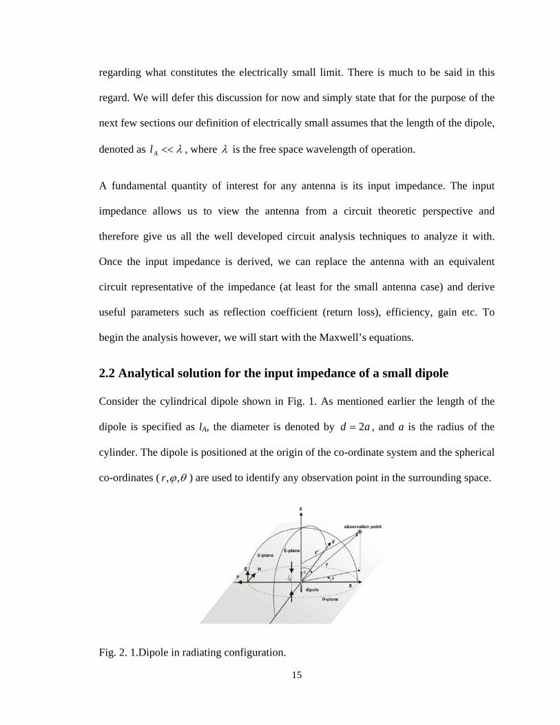
Consider the cylindrical dipole shown in Fig. 1. As mentioned earlier the length of the
dipole is specified as lA, the diameter is denoted by ad 2= , and a is the radius of the
cylinder. The dipole is positioned at the origin of the co-ordinate system and the spherical
co-ordinates ( θϕ,,r ) are used to identify any observation point in the surrounding space.
Fig. 2. 1.Dipole in radiating configuration.

16
Our first attempt at solving for the dipole fields and hence the impedance begins with the
current density being assumed to be constant (an infinitesimally small dipole). To do so
we define the current density to be
2/2/,ˆ)()()( 0 AA lzlIzyxrJ <<−∀= δδ (2.1)
This is shown in Fig. 2.2, graphically,
Fig. 2. 2. Uniform current distribution on the infinitesimally small dipole.
The integral
∫∫∫ ′′′−
′−−= rdrJ
rrrrjk
rA
)(
4)exp(
)( 0 πµ (2.2)
is found analytically as (when 0→l )
( )( ) )exp(
4ˆ
,0,04),0,0exp(
)( 002/
2/
rjkrlI
zzdzr
zrjkrA A
l
l
A
A
−≈′′−
′−−= ∫
− πµ
π (2.3)
The magnetic field is found by taking the curl of the magnetic vector potential
AH
×∇=0
1µ
(2.4)
Before this is done, we first switch to the spherical coordinate system from the current

17
rectangular coordinate system (notice the unit vector for identification). The standard
conversion approach utilizing the matrix-vector notation, is shown in Eq. (2.5).
−−=
z
y
xr
AAA
AAA
0cossinsinsincoscoscos
cossinsincossin
φφθφθφθθφθφθ
φ
θ (2.5)
Since Eq. (2.3) has only the z-component of the magnetic vector potential, we write the
three components in the spherical coordinate system as,
( )
( )
0
sinexp4
sin
cosexp4
cos
00
00
=
−−=−=
−==
φ
θ θπ
µθ
θπ
µθ
A
rjkrlI
AA
rjkrlI
AA
Az
Azr
(2.6)
We now use Eq. (2.4) to calculate the magnetic field H
. The curl expansion in spherical
coordinates is as follows:
( ) ( ) ( )
∂∂
−∂∂
+
∂∂
−∂∂
+
∂∂
−∂∂
=×∇θ
φφθ
θφ
θθθ θφ
θφ
rr AArrr
Arr
Ar
AA
rrA
1ˆ
sin11ˆsin
sin1ˆ
(2.7)
Note, that from Eq. (2.6) the azimuthal component of the vector potential is zero while
the radial and elevation component do not have any azimuthal variation. Applying this
knowledge to Eq. (2.7) we find that only one component exists i.e.
( ) )exp(114
sinˆ1ˆ 0 rjkrjkr
ljkIAAr
rrAH Ar
−
+=
∂∂
−∂∂
=×∇=π
θφ
θµφ θ (2.8)
The electric field is found using the expression for the magnetic field. Ampere’s law
modified by displacement currents JHtE
−×∇=∂∂ε in the phasor form reads (in the
free space where there are no currents)

18
Hj
E
×∇=ωε1 (2.9)
To evaluate Eq. (2.9) we apply the similar procedure as before and recognize that the
radial and elevation components of the magnetic field are zero. The expression for the
curl becomes
( ) ( )
∂∂
−+
∂∂
=×∇ φφ θθθθ
Hrrr
Hr
rH
1ˆsinsin1ˆ (2.10)
Calculating the various partial derivatives in Eq. (2.10) and substituting ηωε =k we get
)exp(1114
sinˆ)exp(112
cosˆ22
02
0 rjkrkrjkr
lkIjrjk
rjkrlI
rE AA
−
−++−
+=
πθη
θπ
θη (2.11)
The radiated power is obtained in the form
[ ]*2
0 0
2 Re21,sin HEPddnPRPrad
×=⋅= ∫ ∫ θθϕ
ππ
(2.12)
which after integration yields
20
202
20
3IRIlP A
rad ≡=λ
πη (2.13)
Therefore, the input resistance R of the small dipole antenna has the form
22
2
20 80
32
==λ
πλ
πη llR A (2.14a)
The reactance of the small dipole antenna may be obtained through the reactive power,
which yields
−−=
A
A
laljX λ
πη
12
ln3
0 (2.14b)
19
where a is the antenna radius for the cylindrical dipole. The reactance is capacitive and
large. The width of the blade dipole t is related to the radius of the equivalent cylindrical
dipole by making the static capacitance equal in both the cases. This yields ([32], p. 514):
dat 24 ==
2.3 Antenna impedance model
For a wire or strip dipole, the input impedance, AZ , can be approximated with a high
degree of accuracy [31] as
32
32
6031967938008261744560)(613115396303246747870)(
)(cot12
ln120)(
z. z.z - ..-zXz.z.z ..-zR
zXza
ljzRZ AA
++≈
+++≈
−
−−=
(2.15a)
In Eq. (2.15a), Al is the dipole length, a is the dipole radius, 2/Aklz = , and λπ /2=k is
the wavenumber. The accuracy of Eq. (2.15a) quickly degrades above the first resonance
[31]; thus, at the high-frequency end, very small dipoles cannot be considered. At the
lower end, Eq. (2.15a) is only valid when the dipole radiation resistance is positive and
does not approach zero. This gives us 2 complex roots which and one real root.
discarding the complex roots, we get the condition
05.00.5
or 07.02/ >>=λ
AA
lklz (2.15b)
If a strip or blade dipole of width t, is considered, then 4/eq ta = [32]. We note here that
a, is the radius of a cylindrical dipole, whilst eqa is the equivalent radius of a wire
approximation to the strip dipole. In this study, the first result is used. Thus, Eq. (2.15a)

20
holds for relatively small non-resonant dipoles and for half-wave dipoles, i.e. in the
frequency domain approximately given by
2.1/05.0 res ≤≤ ffC (2.15c)
where )2/(0res Alcf ≡ is the resonant frequency of an idealized dipole having exactly a
half-wave resonance (c0 is the speed of light) and Cf is the center frequency. When a
monopole over an infinite ground plane is studied, the impedance is half.
2.4 Comparison of impedance model with full wave EM simulation
To confirm the performance of the semi-analytical expression for the impedance behavior
of a dipole, provided in Eq. (2.15a), we plot the resistance and reactance as a function of
frequency (20 - 400 MHz) and compare it to the results from a full wave electromagnetic
simulation model. A dipole of length mm 150=Al and resonant frequency of 1 GHz is
considered. The full wave simulation model is of a blade dipole of appropriate width, t
calculated using the relation dt 2= . To illustrate the difference in the impedance
properties, four cases were considered in which the length to diameter ratios were varied,
i.e. the cases considered were [ ]60,30,10,5.7=dlA .
The resulting data for the resistance and reactance are plotted as a function of frequency
in Fig. 2.3(a)-(d). Overall, there is excellent agreement between the analytical expression
and the full wave simulation model for the reactance. We clearly see that the dipole
thickness (diameter in case of cylinder or the width in the case of a planar (blade) dipole)
has a significant impact on the reactance, namely the thicker dipoles have lower
reactance. The resistance is primarily a function of the total length of the dipole

21
(inclusive of the feed width) and therefore doesn't display any significant variation with
changing radii/widths.
Fig. 2. 3. Comparison between the analytical expression for impedance of a dipole/monopole in Eq. (8a) (solid-blue curve) and the result of a full-wave EM simulation in Ansoft HFSS (dash-dotted red curve). The dipole is resonant at 1 GHz and 4 geometries have been considered (a - d).
2.5 Wideband impedance matching – the reflective equalizer
The reactive matching network is shown in Fig. 2.4(a) [23]. The generator resistance is
fixed at 50Ω . This network does not include transformers. Following Ref. [23], the
reactive matching network is included into the Thévenin impedance of the circuit as
viewed from the antenna, see Fig. 2.4(b).
In fact, the network in Fig. 2.4(a) is not a matching network in the exact sense since it
does not match the impedance exactly, even at a single frequency. Rather, it is a
reflective (but lossless) equalizer familiar to amplifier designers, which matches the
impedance equally well (or equally “badly”) over the entire frequency band. The

22
equalizer network is reflective since a portion of the power flow is always being reflected
back to generator and absorbed. Following Ref. [23], we can consider the generator or
transducer gain in the form
ZZRR
ZT
TA
T
T
22*
2 )(1)()()()(4
load matched-conjugate Power toload Power to)( ω
ωωωω
ω Γ−=+
== (2.16)
The gain T is the quantity to be uniformly maximized over the bandwidth, B. In practice,
the minimum gain over the bandwidth is usually maximized [23], [26].
Fig. 2. 4. Transformation of the matching network: a) reactive matching network representation, b) Thévenin-equivalent circuit representation. The matching network does not include transformers.
The problem may be also formulated in terms of the power reflection coefficient 2)(ωΓ ,
viewing from the generator with the equalizer into the antenna. Obviously, the power
reflection coefficient needs to be minimized. Note that the transducer gain is none other
than the square magnitude of the microwave voltage transmission coefficient. In this text,
we follow the "generator gain" terminology in order to be consistent with the background
research in this area.
23
2.6 Bode-Fano bandwidth limit
The Bode-Fano bandwidth limit of broadband impedance matching ([16], [28]) only
requires knowledge of the antenna’s input impedance; it approximates this impedance by
one of the canonic RC, RL, or RLC loads ([16], and [28], p. 262). The input impedance
of a small- to moderate-size dipole or monopole is usually very similar to a series RC
circuit, as seen from Eq. (2.15a). When 5.0/ res ≤ffC or 75.02/ <= Aklz (a small
antenna or an antenna operated below the first resonance), the antenna resistance is
usually a slowly-varying function of z (almost a constant) over the limited frequency
band of interest whereas the antenna’s reactance is almost a pure capacitance. This
observation is valid at a common geometry condition: ( ) 5.1)2/(ln >alA . The Bode-Fano
bandwidth limit for such a RC circuit is written in the form [28] and restated here in Eq.
2.17. Fig. 2.5 illustrates the equivalent circuit for the electrically short antenna and an
appropriate matching circuit to be found so as to achieve the input reflection coefficient
level ( )ωΓ .
RCd∫∞
<
Γ02 )(
1ln1 πωωω
(2.17)
Fig. 2. 5. Low frequency RC circuit model for an electrically short dipole/monopole antenna.
24
Note, that Eq. (2.17) does not depend on the matching network (other than the fact that it
is assumed to be passive and lossless) or on the source. It is purely a function of the load
alone. For a rectangular band-pass frequency window ]2/,2/[ BfBf CC +− of
bandwidth B and centered at Cf , with 0TT = within the window and 0=T otherwise,
Eq. (2.17) and Eq. (2.15a) allow us to estimate approximately the theoretical limit to the
gain-bandwidth product as long as the dipole or monopole size remains smaller than
approximately one quarter or one eight wavelength, respectively. This is shown in Fig.
2.6 along with two other realizations that illustrate the utilization of the available
matching area in terms of the gain and bandwidth sought.
2.7 Gain-bandwidth product (small fractional bandwidth, small gain)
Let us first obtain the simple closed-form estimate for the gain bandwidth product. Using
the expression for gain, T, in terms of power reflection coefficient 2)(ωΓ , in Eq. (2.16)
we rewrite Eq. (2.17) as,
RCdT∫
∞
<
−0
2 11ln1 πω
ω (2.18)
Substituting 0TT = over the bandwidth B and applying the appropriate limits for ω to
the integral in Eq. (2.18) we arrive at
RCdT
U
L
∫ <
−
ω
ω
πωω 2
0
11
1ln , BfBf CUCL ππωππω +=−= 2,2 (2.19)
Solving the integral in (2.19) yields
( ) ( )
BBfRC
T C
24
1ln21 222
0−
>−−π (2.20)

25
Fig. 2. 6. Illustration of different gain-bandwidth realizations and the corresponding matching areas under the ideal, constant reflection coefficient/constant transducer gain assumption.
Next, we assume the fractional bandwidth CfBB /= to be small, i.e. 1.0<B ; we also
assume that 10 <<T . We then simplify the inequality in Eq. (2.20) by using the Taylor
series expansion of the terms on the left hand side as follows
( ) T
TT
+−−−=−−
2211ln
21 2
000 (2.21)
Ignoring the higher order terms and rewriting the resulting expression in terms of B as
follows:
( ) ff
z
alf
fzRRCfB
RCfTT C
A
CC
C
resres
20
0 2,
12
ln
1480
)(,2
21ln
21 ππ
=
−
Ω≈>≈−− (2.22)
In Eq. (2.22), we have replaced the geometric mean of the upper and lower band
frequencies by its center frequency, which is valid when i) 25.0<B ; ii) the half-
wavelength approximation for dipole's resonant frequency is used; and iii) dipole's
capacitance in the form
−×Ω≈− 1
2ln480 res
1
alfC A is chosen. The last approximation

26
follows from Eq. (2.15a) when z is at least less than one half. Thus, from Eq. (2.22) one
obtains the upper estimate for the gain-bandwidth product in the form
ff
z
alf
fzRBT C
A
C
resres
20 2
,1
2ln
1480
)(4 ππ =
−
Ω< (2.22a)
The value of this simple equation is in the fact that the gain-bandwidth product is
obtained and estimated explicitly. Unfortunately, Eq. (2.22a) is limited to small
transducer gains.
2.8 The arbitrary fractional bandwidth and gain scenario
The only condition we will exploit here is 5.0/5.0 res <= ffz Cπ . In that case the dipole
capacitance can still be approximately described by the formula from subsection 2.7. The
analysis of subsection 2.7 also remains the same until Eq. (2.20). However, we now
discard the assumption on small transducer gain. We define the fractional bandwidth
CfBB /= as before. After some manipulations Eq. (2.20) yields
( ) ff
z
alf
fzRTB
B C
A
C
resres
2
02 2
,1
2ln
1480
)(41
1ln4/1
ππ =
−
Ω<
−− (2.22b)
This estimate does not contain the gain-bandwidth product BT0 explicitly, but rather
individual contributions of 0T and B . It is valid below the first dipole resonance, and it is
a function of two parameters: the dimensionless antenna geometry parameter )2/( alA
and the ratio of the matching frequency to the antenna's resonant frequency, res/ ffC .
Frequently, the fractional bandwidth is given, and the maximum gain 0T over this
bandwidth is desired. In this case, Eq. (2.22b) can be transformed into

27
( ) ff
z
alB
BffzRT C
A
C
res
2
res
20 2
,1
2ln
4/1480
)(4exp1 ππ =
−
−Ω
−−< (2.22c)
We note that this result does not depend on particular value of the generator’s resistance,
Rg. Fig. 2.7 gives the maximum realizable gain according to Eq. (2.22c) obtained at
different desired bandwidths as a function of matching frequency. In Fig. 2.7 a to c we
have considered three different dipoles, with 50,10,5/2/ == dlal AA , where ad 2= is
the dipole diameter. Also, we observe that the condition ( ) 5.12/ln >alA is satisfied for
every case in Fig. 2.7.
2.9 Dipole vs. monopole
As a first example we consider a short, thick dipole of total length Al =23 cm and
5/ =tlA that is designed to have a passband from 250 to 400 MHz, and a center
frequency of 325 MHz. The resonant frequency of the corresponding infinitesimally thin
dipole is found as MHz650)2/(0res == Alcf ; thus, 5.0/ res =ffC . The fractional
bandwidth is approximately 5.0≈B . According to Fig. 2.7c, this leads to a significant
generator gain of 8.00 ≈T over the frequency band; it corresponds to the squared
reflection coefficient 2.02 =Γ , and yields a return loss of 7dB
( 6.2)1/()1(VSWR =Γ−Γ+= ) that is uniform over the operating frequency band.
Next, we consider a short thick monopole of total length Al =11.5 cm and 5/ =dlA , over
an infinite ground plane; it is designed to have the same passband from 250 to 400 MHz.
The resonant frequency of the corresponding infinitesimally thin monopole is found to be
28
MHz650)4/(0res == Alcf so that again 5.0/ res =ffC . The fractional bandwidth
remains the same, i.e. 5.0≈B . However, the monopole’s impedance is half of the
dipole’s impedance. At first glance, it might therefore appear that one should halve the
argument of the exponent in Eq. (2.22c). This is not true because the argument contains
the product RC. While the resistance R decreases by 0.5, the capacitance C increases by
0.5, and thus the total result remains unchanged. Consequently, the dipole consideration
is always applicable to the monopole of half length, assuming an infinite ground plane.
Unfortunately, the Bode-Fano theory does not answer the question of how to achieve the
above limit, and how far this limit is from practically realizable matching circuits with
reasonably small number of lumped elements.
2.10 Comparison with Chu's bandwidth limit
It is instructive to compare the above results with Chu’s antenna bandwidth limit [33]
conveniently rewritten in Refs.[34], [35]. in terms of tolerable output VSWR of the
antenna and the antenna ka, where a is the radius of the enclosing sphere. For this dipole
example with VSWR=2.6 and 78.02/ == Aklka , the Chu's bandwidth limit is found as
[33] - [35],
( )311
kakaQchu += (2.18)
( )( )( ) S
Ska
kaBWI 21
1
2
2
3 −+
= (2.19)
−+
=
11ln
1
SSQ
BWIIπ (2.20)

29
where S = VSWR. Substituting the values for ka and VSWR the bandwidth estimates are
found to be 34 % and 79 % respectively. Note that while the first estimate is less
optimistic, the second estimate suggests higher bandwidth achievability than the Bode-
Fano model discussed above. The key issue is that it includes an uncertainty in relating
the antenna Q-factor to the antenna’s circuit parameters [34].

30
Fig.2. 7. Upper transducer gain limit for three dipoles (from a to c) of diameter d and length Al as a function of matching frequency vs. resonant frequency of the infinitesimally thin dipole of the same length. The five curves correspond to five fractional bandwidth values 0.05, 0.1, 0.25, 0.5, and 1.0, as labeled in the figure, and have been generated by using Eq. (2.17c).
31
Chapter 3. Equalizer circuit development for the non-resonant dipole/monopole like antenna
The theoretical limit on wideband matching derived in chapter 2 is extremely useful to
estimate the quality of the matching network in terms of the transducer gain. However,
this is ultimately a limit and neither it nor the theoretical background suggests ways to
achieve this limit (much like Shannon's limit in communication theory). Within the
sections of this chapter we will develop a wideband matching network for the non-
resonant dipole/monopole. In doing so, we first delve into the single and double tuning
networks. The proposed wideband matching network will then be introduced and the
investigation objectives will be stated.
3.1 Single and double tuning for the electrically short dipole
A small relatively-thin monopole (whip monopole) or a small dipole is frequently
matched with a simple L-matching double-tuning section [30]. This section is shown in
Fig. 3.1a. Ohmic losses of the matching circuit, oR , are mostly due to losses in the series
inductor, which may be the larger one for very short antennas. Namely, 1L might be on
the order of 0.1-1.0 mH for HF and VHF antennas. In this UHF-related study, we will
neglect those losses. The single tuning circuit is also shown as another alternative in Fig
3.1b. In this circuit we get rid of the series inductor L1. Naturally, the expectation here is
that this approach will step up the impedance presented by the antenna.

32
Fig. 3. 1. A whip-monopole with double tuning (L-tuning) [30] and the single tuning network. Ohmic resistance of the series inductor, oR , will be neglected. The matching network does not show the DC blocking capacitor in series with L2.
The goal is to tune the dipole antenna to 50 Ohm or to another real impedance at a
desired frequency of interest, Cf . This frequency is the center band frequency of the
antenna. For tuning, it does not really matter if the antenna is in the transmitting or in the
receiving mode.
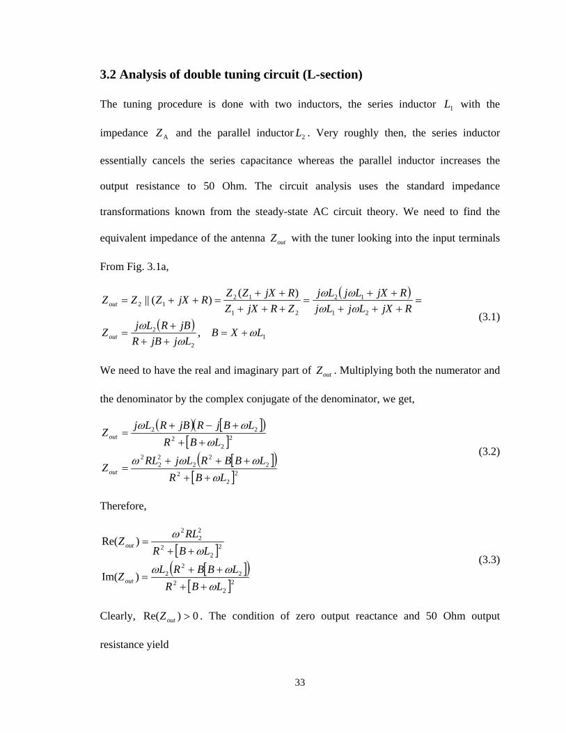
33
3.2 Analysis of double tuning circuit (L-section)
The tuning procedure is done with two inductors, the series inductor 1L with the
impedance AZ and the parallel inductor 2L . Very roughly then, the series inductor
essentially cancels the series capacitance whereas the parallel inductor increases the
output resistance to 50 Ohm. The circuit analysis uses the standard impedance
transformations known from the steady-state AC circuit theory. We need to find the
equivalent impedance of the antenna outZ with the tuner looking into the input terminals
From Fig. 3.1a,
( )
( )1
2
2
21
12
21
1212
,
)()(||
LXBLjjBR
jBRLjZ
RjXLjLjRjXLjLj
ZRjXZRjXZZRjXZZZ
out
out
ωω
ωωωωω
+=+++
=
=+++++
=+++++
=++= (3.1)
We need to have the real and imaginary part of outZ . Multiplying both the numerator and
the denominator by the complex conjugate of the denominator, we get,
( ) [ ]( )[ ]
[ ]( )[ ]22
22
22
22
2
22
222
LBRLBBRLjRLZ
LBRLBjRjBRLjZ
out
out
ωωωω
ωωω
+++++
=
+++−+
=
(3.2)
Therefore,
[ ][ ]( )
[ ]222
22
2
22
2
22
2
)Im(
)Re(
LBRLBBRLZ
LBRRLZ
out
out
ωωω
ωω
++++
=
++=
(3.3)
Clearly, 0)Re( >outZ . The condition of zero output reactance and 50 Ohm output
resistance yield

34
[ ]( )
[ ]50
0
22
2
22
22
2
=++
=++
LBRRL
LBBR
ωω
ω (3.4)
Two unknowns are B and 2L . We denote 2Lω by X1. Eqs. (3.4) are transformed to the
form
502 2
1122
21
122
=+++
−=+
XBXBRRX
BXBR (3.5)
Further transformation gives
501
21
21
122
=+
−=+
BXXRX
BXBR (3.6)
or, which is the same,
)(50 11
122
BXRXBXBR+=
−=+ (3.7)
Clearly,
( )
)50(1
5050
5050
2
222
1
RRRB
RBBR
RBX
−±=−Κ
±=⇒
−=ΚΚ=+
−=
(3.8)
Inserting the negative solution for B into X1 we get,
)50(5021 R
RLX−
== ω (3.9)
Using the relation 1LXB ω+= , we extract for the second component

35
( )RRXL −−−= 501ω (3.10)
Quantitatively from Eqs. 3.9 and 3.10, and referring to Fig. 3.1a, the analytical result for
the tuning inductances has the form for Cgo RR ωω =Ω== and,50,0 , (also see Ref.
[30])
42
,1
12
2222
12CCg
g
C
RLLXLRR
RRL
ωωω−−−−=
−= (3.11)
3.3 Sensitivity of the double tuning circuit
As noted in the prior section, the double tuning circuit for the electrically short dipole
comprises two inductors arranged in a specific configuration as shown in Fig. 3.1 (a). The
solution for the inductor values were derived in section 3.2 and shown in Eq. (3.11). Thus
we can calculate the inductor values in a straightforward manner, if we know the dipole
dimensions (see chapter 2, Eq. (2.10a)) and the generator resistance to be matched
(typically 50 Ω ). However, it is rarely the case that the inductor values predicted by
theory can be found in the real world. In fact even the actual inductor value, if found,
would have an associated tolerance specified.
It is worthwhile to investigate the effect of this variability on the tuning. This is done by
observing the effective resistance and reactance at the input to the double tuning network
due to the variations in inductor values. We consider a 150mm long thin dipole
( 60=dlA ), whose resonant frequency is 1 GHz. In Fig. 3.2, the reactance and resistance
map is plotted as a function of variations from the nominal value of L1 and L2.
Additionally, this map is shown for different choices of center frequency ( Cf ). The
center frequencies satisfy the limiting condition 5.0/ res ≤ffC for an antenna operated

36
below the first resonance. The nominal values for the inductors in the double tuning
network are shown as a green circle in the plots.
The sensitivity maps clearly reveal the difficulty in maintaining a good impedance match
at lower frequencies with the double tuning network. The reactance and resistance maps
and the associated 3D surface plots in Figs. 3.2 and 3.3 show that the margin of error, for
the double tuning network improves with increasing center frequency. In Fig. 3.3 for
the Cf = 0.1 GHz case, the nominal values for inductance calculated by using Eq. 3.11
are precariously positioned over the dip in the reactance surface. On either side of this
dip, the total reactance at the input to the network becomes large very quickly.
Expectedly, it is the opposite behavior for the resistance wherein, the nominal values for
inductance result in a sharp peak for the input resistance. In both cases, it is the sensitivity
to L1 that can cause more damage. At higher frequencies, the sensitivity function spreads
out and the gradient close to the nominal values of the inductance becomes smoother in
the case of the resistance. The reactance behavior is improved and shows some immunity
to small variations in L1.
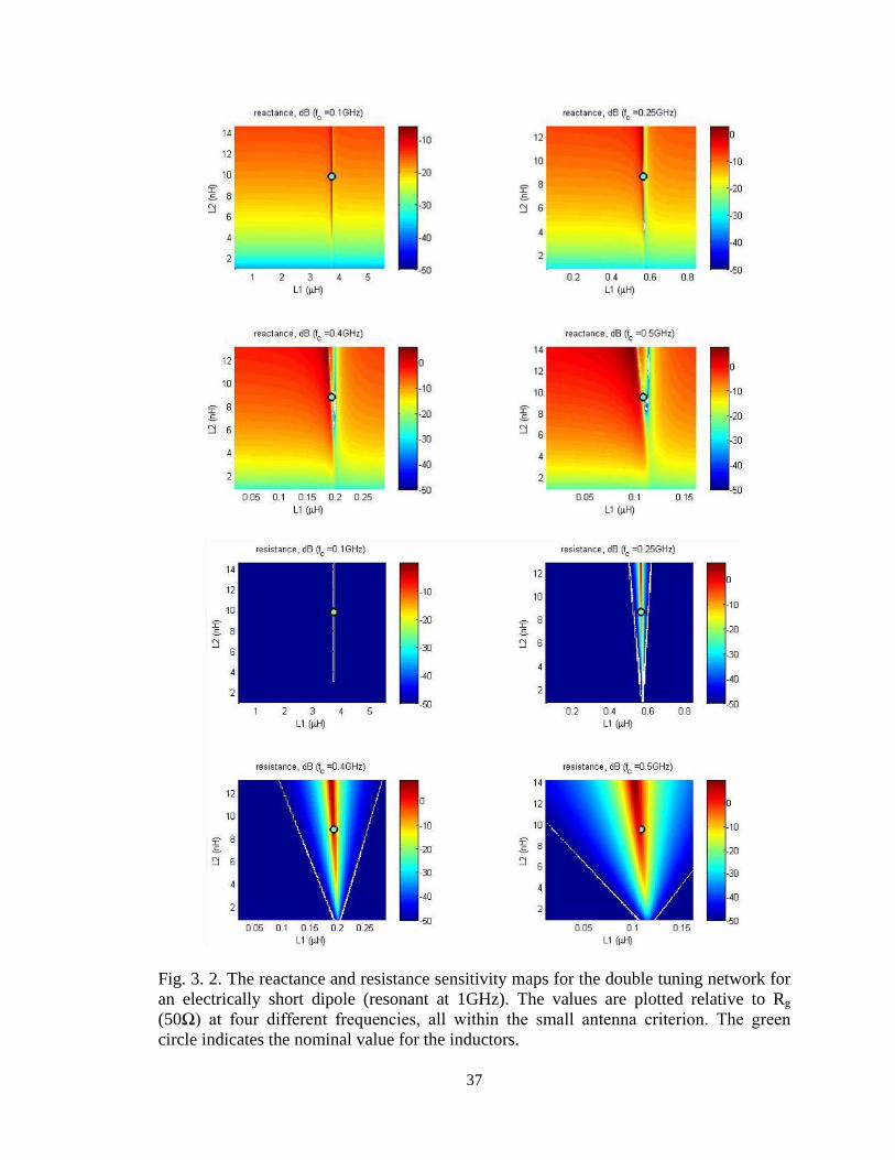
37
Fig. 3. 2. The reactance and resistance sensitivity maps for the double tuning network for an electrically short dipole (resonant at 1GHz). The values are plotted relative to Rg (50Ω) at four different frequencies, all within the small antenna criterion. The green circle indicates the nominal value for the inductors.

38
Fig. 3. 3. The three dimensional plot for reactance and resistance sensitivity of an electrically short dipole (resonant at 1GHz). The variation in the surface features of each function can be seen for four different frequencies. The green circle indicates the nominal value for the inductors.

39
In the case of different values of the generator resistance, the sensitivity plots in Fig. 3.4
and 3.5 clearly show that the underlying behavior is similar. At 0.1 GHz, the center
frequency at which the double tuning network values are calculated, the reactance and
resistance plots do not vary drastically due to changes in the generator resistance. It is to
be noted that changes to the generator resistance affect only L2, the shunt inductor.
Therefore, we see that larger values of Rg, demand a bigger inductance. It is reasonable to
expect that for higher center frequency of matching, the nominal inductance value will
not be as large (owing to the larger antenna radiation resistance to begin with).
Changes to the thickness of the dipoles (or width in the case of the blade dipoles), does
change the sensitivity maps for reactance and resistance. The Figs. 3.6 and 3.7 show plots
of this variation at a center frequency of 0.5 GHz. The thinner dipoles (e.g. 60=dlA )
are again the worse of the four cases considered. The reason is clear; the thicker dipoles
have lesser capacitive reactance and this directly affects the series inductor L1 in the
double tuning network.
3.4 Analysis of single tuning circuit
The single tuning is made with the inductor 2L in parallel. The inductance 1L is exactly
zero. From Eq. (3.3) one has
[ ]ω
ωX
XRLLXXR−+
=⇒=++22
222 0 (3.12)
and the resistance then becomes (B=X as long as 1L is zero)
[ ] [ ] RXR
XXRRXRR
LXRLR
LBRLRZout
22
2242
222
22
2
22
2
22
2
22
2
)/()()Re( +
=+
+=
++=
++=
ωω
ωω (3.13)

40
The result implies that the available feed point resistance of the antenna is simply stepped
up by the factor Χ , where
RXR 22 +
=Χ (3.14)
Thus, the single degree of freedom allows for achieving either a zero input reactance and
an arbitrary resistance transformation as given by Eq. (3.14), or a possible 50Ω input
resistance with an non-zero transformed input reactance (a similar transformation can be
derived by considering the alternative case of ReZin=50Ω ).

41
Fig. 3. 4. The reactance and resistance sensitivity maps for the double tuning network for an electrically short dipole (resonant at 1GHz). The values are plotted relative to four different values of Rg at fC = 100 MHz. The green circle indicates the nominal value for the inductors.

42
Fig. 3. 5. The three dimensional plot for reactance and resistance sensitivity of an electrically short dipole (resonant at 1GHz). The surface features of each function can be seen for four different values of generator resistance. The green circle indicates the nominal value for the inductors.
43
Fig. 3. 6. The reactance and resistance sensitivity maps for the double tuning network for an electrically short dipole (resonant at 1GHz). The values are plotted relative to four different values of 60=dlA at fC = 0.5 GHz. The green circle indicates the nominal value for the inductors.

44
Fig. 3. 7. The three dimensional plot for reactance and resistance sensitivity of an electrically short dipole (resonant at 1GHz). The surface features of each function can be seen for four different values of generator resistance. The green circle indicates the nominal value for the inductors.

45
3.5 Extension of the L-section matching network
To increase the bandwidth of the L-tuning section at some fixed values of 21 , LL , we
suggest to consider the matching circuit shown in Fig. 3.8. It is seen from Fig. 3.8 that
we can simply add a high-pass T-network with three lumped components (a shunt
inductor and two series capacitors) to the L-section or, equivalently, use two sections of
the high-pass LC ladder and investigate the bandwidth improvement. The Thévenin
impedance of the equalizer, as seen from the antenna, is given by
sCsCRsL
sCRsLZ
RZsL
ZsLZsL
Zg
gg
gg
g
gT
+++
+=
=+
+= )/(1
))/(1())/(1(
II case
I case,
354
5412
2 (3.15)
where ωjs = . The default values of the circuit parameters for the sole L-tuning section
read ∞=== 543 CLC . Thus, we introduce three new lumped circuit elements, but avoid
using transformers. Instead of using impedances, an ABCD matrix approach would be
more beneficial when using transformers.
Fig. 3. 8. An extension of the L-tuning network for certain fixed values of 21 , LL by the T-match.

46
3.6 Objectives of the circuit optimization task
We assume that the antenna is to be matched over a certain band B centered at Cf , and
that the gain variation in Eq. (2.16) does not exceed ±25% over the band. If, for this
given equalizer circuit, we cannot achieve such small variations at any values of the
circuit parameters, the equalizer is not considered capable of wideband impedance
matching over the bandwidth B. We know that a low-order equalizer (the L-matching
section) alone is not able to provide a nearly uniform gain over a wider band. However,
increasing the circuit order helps. Thus, two practical questions need to be answered:
A. For a given center frequency Cf and bandwidth B, or for a given fractional
bandwidth CfBB /= , what are the (normalized) circuit parameters that give
the required bandwidth?
B. What is the gain-bandwidth product and how does it relate to the upper
estimate given by Eq. (2.22c)?
Yet another important question is the phase linearity over the band; this question will not
be considered in the present study.
3.7 Numerical method and the antenna parameters tested
To optimize the matching circuit with 5 lumped elements we employ a direct global
numerical search in the space of circuit parameters. The grid in 5ℜ space includes up to
5100 nodes. The vector implementation of the direct search is fast and simple, but it
requires a large (64 Gbytes or higher) amount of RAM on a local machine.
For every set of circuit parameters, the minimum gain over the bandwidth is first
calculated [23]. The results are converted into integer form and sorted in a linear array, in

47
descending order, using fast sorting routines on integer numbers. Then, starting with the
first array element, every result is tested with regard to ±25% acceptable gain variation.
Among those that pass the test, the result with the highest average gain is finally retained.
After the global maximum position found on a coarse mesh, the process is repeated
several times on finer meshes in the vicinity of the anticipated circuit solution.
We will consider the dipole case and assume monopole equivalency. The set of tested
antenna parameters includes:
]50.0:05.0:05.0[/],5.0,1.0[],5,10,50[/ res === ffBdl CA (3.16)
3.8 Alternative optimizers
A viable alternative to the direct global numerical search used in this study, which is also
a derivative free and a global method, is the genetic algorithm [36]. The genetic
algorithm (GA) belongs to a class of stochastic optimization algorithms that attempt to
mimic some of the classical evolutionary processes that occur in the biological world.
Processes such as reproduction, mutation and crossover, which are central to the
evolution of a species in nature hold the same meaning when applied for the purpose of
optimization. The striking feature of GA based optimization is that we begin with a
population of possible candidates for the solution, thereby introducing an inherent
parallelism into the process. The optimality of this population is tested by applying it to
the fitness function (also known as the objective function to be optimized). Depending on
the results, candidates are selected to populate the second generation by applying the
three key processes mentioned earlier. This process repeats itself till either a good
solution is found or a solution to the problem is deemed infeasible. GA's have been
widely used in many fields including antenna array design [37] and electromagnetics

48
[38]. An interesting application of the GA was reported in ref. [39] wherein the authors
have demonstrated its use in optimizing lumped component networks for an antenna
synthesis application as well as the matching network.
The MATLAB © based Genetic Algorithm and Direct Search toolbox™ [40], provided us
with an excellent platform to optimize the matching circuit under consideration in this
study. This toolbox features a vast array of choices with which we were able to tailor the
GA solver for our requirement. The results obtained from this GA are rather close to
those achieved by the direct global numerical search and further work may be pursued in
this direction. While the genetic algorithm by itself is a good candidate for a global
optimizer, a direct search technique known as 'Pattern search' can be used with it to
improve its performance. This is known as a hybrid GA [40] and it works by taking the
best solution arrived at by the GA as the initial point and proceeds to refine the result by
searching along a 'pattern'. The pattern here refers to a set of vectors that define the
parameter space (in our case the circuit parameters) for the current iteration over which
the search is performed. Depending on the result from the objective function this set of
vectors is expanded or contracted by specific amount and the process repeats. To use this
method we first generated a population of random candidate solutions with a uniform
distribution, for the circuit parameters. The GA solver then tests these candidate solutions
based on a specified criterion, which in this particular case, is to maximize the minimum
gain over the band. After assigning scores to the various candidate solutions, it then
creates the next generation of solutions, referred to as the 'children', by pairing candidate
solutions from the previous generation, referred to as the 'parents'. To ensure diversity in
the next generation, mutations, or random changes to one of the parents in a pair are

49
introduced. These new solutions replace the current population and the process repeats.
Several options for stopping criterion can be used such as time limit, no. of successive
generations or even simply the change in the value objective function between two
generations. During this study, the results obtained with the GA toolbox were found to be
in good agreement with the results obtained with the direct global numerical search. In
the next section a comparison of the performance of our direct search routine with the
algorithms from the GA toolbox will be presented.

50
Chapter 4. Numerical simulation and experimental results In chapter 3 the wideband matching network was developed starting with the narrowband
L-section. The circuit optimization task was identified and put forth. To solve for the
network components a direct search based optimization scheme was used. A potential
alternative to the direct search based approach was also proposed in the form of the
Genetic algorithm. The results of the direct search based numerical simulations will be
presented in this chapter. A variety of matching scenarios will be considered. The
practicality of this network lies in whether the components can be procured easily. To
investigate this, a comprehensive search across different antenna geometries and
component sensitivities is made and tabulated. Also presented is a comparison between
the performances of the network proposed in this thesis and a more advanced form of
Carlin’s equalizer [26]. This is done using both the direct search routine and the MATLAB
© based Genetic Algorithm and Direct Search toolbox™ [40]. Finally experimental
results are presented together with a discussion on the same.
4.1 Realized gain – wideband matching for 5.0=B
Fig. 4.1 shows the realized average generator gain over the passband based on the ±25%
gain variation rule at different matching center frequencies. Three dipole geometries with
5,10,50/ =dlA are considered. The bandwidth is fixed at 5.0=B ; we again consider
three dipoles of different radii/widths. The realized values are shown by circles; the ideal
upper estimate from Fig. 2.7 is given by solid curves. One can see that the 5-element
equalizer performs rather closely to the upper theoretical limit 0T when the average gain
51
over the band, T , is substituted instead. For the majority of cases, the difference between
0T and T is within 30% of 0T . The sole L-section was not able to satisfy the ±25% gain
variation rule in all cases except the very last center frequency for the thickest dipole.
4.2 Gain and circuit parameters – wideband matching for
5.0/,5.0 res == ffB C
Table 1a reports circuit parameters of the equalizer for three dipoles with
5,10,50/ =dlA . In every case, matching is done for 5.0/ res =ffC , 5.0≈B . Fig. 4.2
shows the corresponding gain variation with frequency within the passband. In Table 1,
we have presented all circuit parameters for a 23 cm long dipole. To scale parameters to
other antenna lengths one needs to multiply them by the factor 23.0/Al m. Table 1 also
shows the anticipated gain tolerance error. Whilst the average gain itself does not
significantly change when changing capacitor/inductor values, the gain uniformity may
require extra attention for a thin dipole (second row in Table 1). For thicker dipoles (third
and fourth row of the table) one solution to the potential tolerance problem is to slightly
overestimate the circuit parameters for a better tolerance. Generally, the usual uncertainty
in low-cost chip capacitors and chip inductors seems to be acceptable. Table 1 also
indicates that the equalizer for a wideband matching of the dipole does not involve very
large inductors (and large capacitors) and is thus potentially low-loss.

52
Table 4. 1. Circuit parameters and gain tolerance for a short dipole with the total length Al =23 cm. Matching is done for 5.0/ res =ffC , 5.0≈B based on the ±25% gain
variation rule.
Antenna
geometry
dlA /
Circuit parameters Gain/Variance
over the band
Gain/Variance
over the band at
+5% parameter
variation
Gain/Variance
over the band at -
5% parameter
variation
50
1761 =L nH
702 =L nH
9.43 =C pF
804 =L nH
3.155 =C pF
20.0=T
%25/ <∆ TT
19.0=T
%27/ <∆ TT
20.0=T
%38/ <∆ TT
10
4.721 =L nH
7.482 =L nH
6.393 =C pF
1024 =L nH
2.105 =C pF
36.0=T
%24/ <∆ TT
35.0=T
%19/ <∆ TT
38.0=T
%35/ <∆ TT
5
5.211 =L nH
6.242 =L nH
9.613 =C pF
5374 =L nH
3.155 =C pF
60.0=T
%25/ <∆ TT
59.0=T
%19/ <∆ TT
61.0=T
%34/ <∆ TT
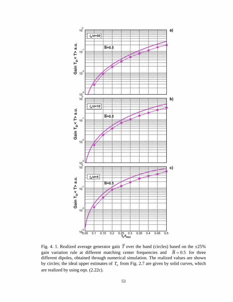
53
Fig. 4. 1. Realized average generator gain T over the band (circles) based on the ±25% gain variation rule at different matching center frequencies and 5.0=B for three different dipoles, obtained through numerical simulation. The realized values are shown by circles; the ideal upper estimates of 0T from Fig. 2.7 are given by solid curves, which are realized by using eqn. (2.22c).

54
4.3 Gain and circuit parameters – narrowband matching for 1.0=B
It is not the subject of this study to discuss the narrowband matching results; however,
they have been obtained and may be discussed briefly. When the two-element L-section
network is able to provide us with the required match, its performance is not really
distinguishable from that of the full 5-element equalizer. However, it does not always
happen that the reduced L-section equalizer is able to do so. The full equalizer is the only
solution at smaller resonant frequencies and for thinner dipoles.
Unfortunately, the deviation from the Bode-Fano maximum gain may be higher for
narrowband matching than for the wideband matching; in certain cases it reaches 100%.
It is not clear whether this high degree of deviation is due to the numerical method or if it
has a physical nature.
4.4 Gain and circuit parameters – wideband matching
for 15.0/,5.0 res == ffB C
A more challenging case is a smaller wideband dipole; we consider here the case when
15.0/ res =ffC and refer to the corresponding theoretical curves presented in Fig. 2.7.
Fig. 4.3 shows the transducer gain variation with frequency within the passband, after the
equalizer has been applied based on the ±25% gain variation rule. The circuit parameters
indicate a higher value of μH46.21 =L for 50/ =dlA and μH06.11 =L for 10/ =dlA .
For 5/ =dlA , inductance 4L attains a larger value of μH40.1 .

55
4.5 Comparison with the results of Ref. [26]
In Ref. [26] a similar matching problem was solved for a thin dipole of length =Al 0.5 m
and the radius a of 0.001m. Matching is carried out for 416.0/ res =ffC , 4.0=B . A
Carlin’s equalizer with an extra LC section has been considered. Fig. 4.4 reports the
performance of our equalizer for this problem (dashed curve). The thick solid curve
within the passband is the corresponding result of Ref. [26] (and copied from Fig. 6). In
our case, the optimization was done based on the ±25% gain variation rule. The
difference between the two average band gains was found to be 5%. The circuit
components for our circuit are 1.06µH, 0.21 µH, 20 pF, 0.95µH, and 17 pF. Note that
without the extra LC section, the Carlin’s equalizer may lead to a considerably lower
passband gain than the gain shown in Fig. 4.4 [26]. Without any equalizer, the
performance is expectedly far worse. The plot indicates that a 20 dB improvement is
achieved at the lower edge of the band and approximately 10 dB at the upper band edge,
when the equalizer is used.
In Fig. 4.5 we show the performance of the MATLAB © based Genetic Algorithm and
Direct Search toolbox™ [40] in comparison with the direct global numerical search for
the same matching problem as in [26]. The Genetic algorithm is used in conjunction with
the patternsearch algorithm and yields a solution with an average band gain variation of
24.67 %. It is noted that the performance is very close to the direct global numerical
search. The component values produced by the GADS toolbox are (in order L1 – C5):
1.09 µH, 0.18 µH, 95.3 pF, 0.99 µH, 11.34 pF. Note, that all component values but for C3
are very similar to that produced by the direct global numerical search.

56
Fig. 4. 2. Gain variation with frequency for a short dipole or for an equivalent monopole at different thicknesses/widths obtained by numerical simulation which uses Eq. (2.16). Matching is done for 5.0/ res =ffC , 5.0≈B based on the ±25% gain variation rule. Vertical lines show the center frequency and the passband.

57
Fig. 4. 3. Gain variation with frequency for a short dipole or for an equivalent monopole at different thicknesses/widths obtained by numerical simulation which uses Eq. (2.16). Matching is done for 15.0/ res =ffC , 5.0≈B based on the ±25% gain variation rule. Vertical lines show the center frequency and the passband.

58
Fig. 4. 4. Gain variation with frequency for a short dipole or for an equivalent monopole of length 0.5 m and radius of 0.001m, by numerical simulation of associated matching network. Matching is done for 416.0/ res =ffC , 4.0=B based on the ±25% gain variation rule (dashed curve). The thick solid curve is the result of Ref. [25] with the modified Carlin’s equalizer, which was optimized over the same passband for the same dipole. Vertical lines show the center frequency and the passband. Transducer gain, in the absence of a matching network, is also shown by a dashed curve following Eq. (2.16).
Fig. 4. 5. Comparison between the results from the genetic algorithm (solid blue curve), and the direct global numerical search algorithm (dashed blue curve) for an equivalent monopole of length 0.5 m and radius of 0.001m, by numerical simulation of associated matching network.

59
4.6 Effect of impedance transformer
A set of numerical simulations for the same dipoles with a 4:1 ideal transformer has
shown that the wideband matching results (achievable gain) are hardly affected by the
presence of a transformer, even though the parameters of the matching circuit change
considerably. For example, in the case of 5.0=B , 15.0/ res =ffC and discussed above,
the average gain without and with transformer is 0.0092/0.0092, 0.020/0.020, and
0.036/0.040 for the three dipoles with 5 ,10,50/ =dlA .
4.7 Experiment - Short blade monopole
We have designed, constructed, and tested a number of short blade monopole test
antennas and the corresponding matching networks. The antenna's first resonant
frequency is in the range 550-650 MHz. The matching is to be done over a wide, lower
frequency band of 250-400 MHz, with the center frequency of 325 MHz. For every
monopole, the ratio, dlA / , equal to 20 has been used in the experiment. Fig. 4.6 shows
the generic monopole setup.
Fig. 4. 6. A 10.1cm long and 2.3cm wide blade monopole over a 1×1 m ground plane used as a test antenna for wideband impedance matching.
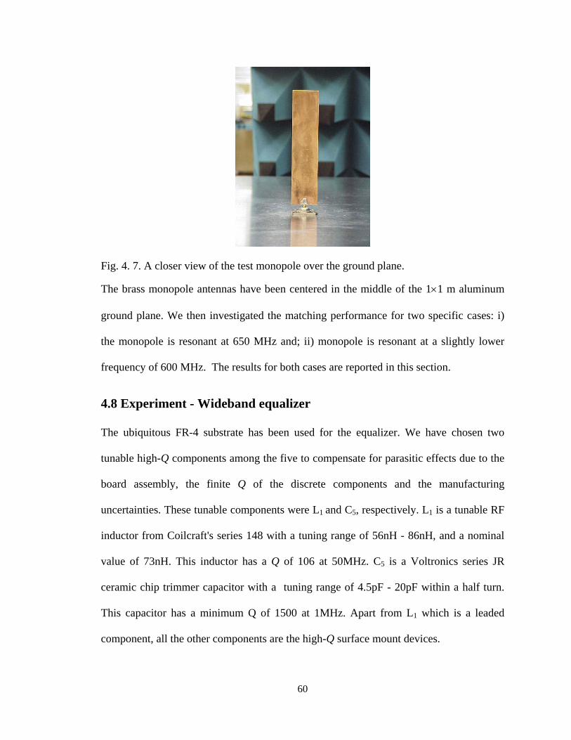
60
Fig. 4. 7. A closer view of the test monopole over the ground plane.
The brass monopole antennas have been centered in the middle of the 1×1 m aluminum
ground plane. We then investigated the matching performance for two specific cases: i)
the monopole is resonant at 650 MHz and; ii) monopole is resonant at a slightly lower
frequency of 600 MHz. The results for both cases are reported in this section.
4.8 Experiment - Wideband equalizer
The ubiquitous FR-4 substrate has been used for the equalizer. We have chosen two
tunable high-Q components among the five to compensate for parasitic effects due to the
board assembly, the finite Q of the discrete components and the manufacturing
uncertainties. These tunable components were L1 and C5, respectively. L1 is a tunable RF
inductor from Coilcraft's series 148 with a tuning range of 56nH - 86nH, and a nominal
value of 73nH. This inductor has a Q of 106 at 50MHz. C5 is a Voltronics series JR
ceramic chip trimmer capacitor with a tuning range of 4.5pF - 20pF within a half turn.
This capacitor has a minimum Q of 1500 at 1MHz. Apart from L1 which is a leaded
component, all the other components are the high-Q surface mount devices.
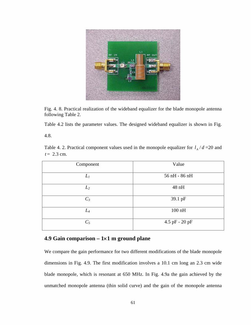
61
Fig. 4. 8. Practical realization of the wideband equalizer for the blade monopole antenna following Table 2.
Table 4.2 lists the parameter values. The designed wideband equalizer is shown in Fig.
4.8.
Table 4. 2. Practical component values used in the monopole equalizer for dlA / =20 and t = 2.3 cm.
Component Value
L1 56 nH - 86 nH
L2 48 nH
C3 39.1 pF
L4 100 nH
C5 4.5 pF - 20 pF
4.9 Gain comparison – 1×1 m ground plane
We compare the gain performance for two different modifications of the blade monopole
dimensions in Fig. 4.9. The first modification involves a 10.1 cm long an 2.3 cm wide
blade monopole, which is resonant at 650 MHz. In Fig. 4.9a the gain achieved by the
unmatched monopole antenna (thin solid curve) and the gain of the monopole antenna
62
with the designed wideband equalizer (thick dotted curve), respectively are shown. The
average transducer gain achieved in experiment is 0.262 over the bandwidth 250MHz -
400MHz with a gain variation of 40 %. The L1 and C5 values for this particular result are
86 nH and 7.63 pF respectively.
Next, we consider a blade monopole antenna of length 10.8 cm and width 2.3 cm. This
blade monopole resonates at 600MHz. Fig. 4.9b shows the matching performance with
(thick dotted curve) and without (thin solid curve) the wideband equalizer. We see that
the equalizer performs rather well even under this scenario and achieves a gain of 0.259
within the bandwidth of interest. The gain variation over the band is 28.8 %. In this case
the value of L1 is changed to 73nH while the capacitance C5 is unchanged.
Here, we also notice an approximate 10dB improvement over the unmatched antenna,
provided by the equalizer at the lower edge of the band. During the experiments we have
noticed that a resonance may appear at lower frequencies below 200 MHz. The
theoretically predicted gain is shown by thick solid curves in Fig. 4.9a and 4.9b.
Generally the experiment follows the theory. In the case of Fig. 4.9a, the average
experimental gain over the band is 0.262 and is slightly higher than the corresponding
theoretical value of 0.245. In the case of Fig. 4.9b, the average experimental gain over the
band is 0.259 versus the theoretical value of 0.245. We believe that the average gain
difference is within the experimental uncertainty. This statement can be further confirmed
by the results from the fourth and fifth column of Table 4.1, where we observe the quite
similar variation when the component values of the matching circuit are varied by ±5%.
However, for the local gain behavior, we observe somewhat larger variations. The
experimental gain is higher in the middle of the band, but is lowered at the band edges.

63
We explain these variations by the associated tuning procedure and by the inability to
exactly follow the requested values of inductance L1 and capacitance C5. An additional
important mechanism is lumped-element losses at the higher band end. Yet one more
uncertainty factor is due to a relatively small size of the measurement chamber. This
effect becomes apparent at low frequencies as Fig. 4.9 indicates. The present results are
preliminary and have a very significant room for improvement.
Fig. 4. 9. The experimental gain data (dotted curve 1) in comparison with the theoretical result (thick curve 2) for two blade monopoles with the matching network from Table 2: a) - the blade length is 10.1 cm and the width is 2.3 cm; b) - the blade length is 10.8 cm and the width is 2.3 cm. The thin solid curve 2 in this graph corresponds to the antenna gain (based on the measured return loss) without the matching network.
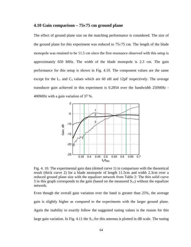
64
4.10 Gain comparison – 75×75 cm ground plane
The effect of ground plane size on the matching performance is considered. The size of
the ground plane for this experiment was reduced to 75×75 cm. The length of the blade
monopole was retained to be 11.5 cm since the first resonance observed with this setup is
approximately 650 MHz. The width of the blade monopole is 2.3 cm. The gain
performance for this setup is shown in Fig. 4.10. The component values are the same
except for the L1 and C5 values which are 60 nH and 12pF respectively. The average
transducer gain achieved in this experiment is 0.2854 over the bandwidth 250MHz -
400MHz with a gain variation of 37 %.
Fig. 4. 10. The experimental gain data (dotted curve 1) in comparison with the theoretical result (thick curve 2) for a blade monopole of length 11.5cm and width 2.3cm over a reduced ground plane size with the equalizer network from Table 2: The thin solid curve 3 in this graph corresponds to the gain (based on the measured S11) without the equalizer network.
Even though the overall gain variation over the band is greater than 25%, the average
gain is slightly higher as compared to the experiments with the larger ground plane.
Again the inability to exactly follow the suggested tuning values is the reason for this
large gain variation. In Fig. 4.11 the S11 for this antenna is plotted in dB scale. The tuning

65
procedure results in better S11 in the middle of the band as compared to the edges thus
resulting in higher transducer gain in that region as observed in Fig. 4.10.
Fig. 4. 11. The experimental S11 data (dotted curve 1) in comparison with the theoretical result (thick curve 2) for a blade monopole of length 11.5cm and width 2.3cm over a reduced ground plane size with the equalizer network from Table 2. The thin solid curve 3 in this graph corresponds to the measured S11 without the equalizer network.
4.11 Discussion on S11
The results shown in Figs. 4.9-4.11 about the transducer gain and the S11, indicate that if
the generator can tolerate an input VSWR in the range 7:1, then using the reflective
equalizer approach can improve the transducer power gain for an electrically short
antenna. However, if the input VSWR requirement needs to be restricted to lie below 4:1
then as discussed in section 2.9 and later in Table 4.1, the dlA / ratio for the antenna
needs to be reduced, which would result in a thicker cylindrical dipole (or monopole) or
alternatively a wider blade dipole (or monopole). Specifically, using an dlA / = 5 for a
similar antenna as considered in the experiments resulted in a higher theoretical
transducer gain and a minimum theoretical VSWR of 2.6:1. By theoretical we imply the
upper limit predicted by using the Eq. 2.22c. In section 4.2, Table 4.1 provides the
component values and the realized transducer gain for our 5 element equalizer. Based on

66
the experimental results for the blade monopoles with dlA / = 20 we can safely predict
that a lower VSWR can be expected for smaller dlA / ratios as well, by using the
reflective equalizer.

67
Chapter 5. Introduction to Modular arrays
The demand for higher bandwidths and gain from antenna systems for communication
and positioning/navigation purpose is on the rise [41]-[44]. With the advent of software
defined radios and cognitive radios, much more will be demanded from the antenna
systems of the future [45]-[47]. While single antenna systems do achieve bandwidths far
greater than an octave, there is a degree of complexity in their design and construction.
Some of the common examples of such antennas are the spiral [48], [49]and the log-
periodic antennas [50]. Antennas like the dipoles, monopoles and patches are relatively
simpler to design and fabricate. The dipoles and monopole antennas have figured
prominently in wide bandwidth designs [51]. Expectedly the directive gain of such
antennas is lower than what can be achieved by using an array.
The design of arrays comprising small number of elements requires a different approach
as compared to the large arrays (so called infinite arrays). Antenna array design with
large number of elements wherein the total number of elements can range anywhere from
100-10000 and higher involves a good choice of the individual element and then
proceeds to an infinite array based simulation. An example of such large arrays is the
Cobra Dane phased array system located in Alaska shown in Fig. 5.1. This system was
developed for tracking the threat of an InterContinental Ballistic Missile (ICBM) attack
on the United States.
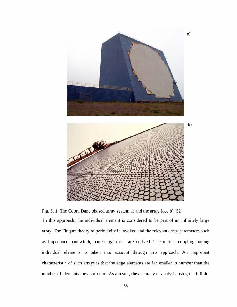
68
Fig. 5. 1. The Cobra Dane phased array system a) and the array face b) [52].
In this approach, the individual element is considered to be part of an infinitely large
array. The Floquet theory of periodicity is invoked and the relevant array parameters such
as impedance bandwidth, pattern gain etc. are derived. The mutual coupling among
individual elements is taken into account through this approach. An important
characteristic of such arrays is that the edge elements are far smaller in number than the
number of elements they surround. As a result, the accuracy of analysis using the infinite
b)
a)

69
array approach, for finite large size arrays increases with the number of elements. One
can expect that the accuracy for a 5000 element array would be higher than one for a 100
element array. This approach is widely used and is well documented [53], [54].
The arrays of smaller sizes such as 2x1, 4x1, 2x2, 4x2, and 4x4 present an interesting set
of challenges. In fact, for these arrays, the edge elements outnumber those bounded by
them (in planar arrays 2x2 is an exception in that all elements are indeed edge elements!).
Thus, these edge elements play a significant role in the overall performance. An infinite
array simulation cannot be expected to accurately represent the performance of such
small arrays. Instead, a finite array based analysis can be employed as suggested in [54]-
[59]. In [60] - [67] , various approaches for the modular design of arrays are suggested.
These approaches however are still oriented towards large size finite arrays.
The contribution of this thesis is to investigate the distributed impedance matching
approach in the design of modular arrays. In doing so, the canonic planar resonant dipole
is used to design the square unit cell (planar dipole over ground plane) such that, the 2x1,
2x2 and 4x1 arrays attain a VSWR of at least 2:1 over a bandwidth of at least 2:1, and
stable gain (directive gain variation ≤ 3dB) over the entire band. The bandwidth definition
used is shown below,
L
U
ff
B = (5.1)
where, Uf and Lf represent the upper and lower frequencies which satisfy the S11 < -10
dB criterion. Furthermore, gain behavior at the lower frequencies in the band is of interest
and it will be compared to the prediction by the array area rule [68]. It is the attempt of
this thesis to show that through careful design we can exploit mutual coupling between

70
the unit cells to enhance the impedance bandwidth and provide for a stable broadside
gain. The modular design approach is an attractive one for the following reasons:
• It is easy to build arrays of a specific configuration, once the individual radiator
has been optimized.
• Individual elements in the array can be easily replaced if a problem develops in
them.
• Since the individual radiator satisfies multiple array configurations, it allows for
flexibility in the deployment of different arrays without loss of performance
The present modular approach may be used for low-cost larger-volume small broadside
array design. The effect of scanning on such arrays has not been investigated.
5.1 Unit Cell Geometry
The unit cell serves as the basic building block for all the arrays and is shown in Fig. 5.2.
It comprises of a resonant dipole of total length 2L, and width W placed over a finite
ground plane of dimensions yx SS × at a height h. The x-axis is along the horizontal in the
Fig. 5.2. A wide blade dipole is chosen since it is easier to impedance match to such
dipoles (thick dipoles if considering cylindrical) [69], [70]. If needed a conical impedance
matching structure could be incorporated within the dipole, providing a smoother
transition from the feed to the wing of the blade dipole. However, this unit cell does not
have such a structure and therefore makes it easier to build. The blade dipole as well as
ground plane need the mechanical support. For this reason, two substrates are provided for
the dipole element and the ground plane respectively. In addition, 4 supporting posts are
located at the corners of the unit cell in between the dipole and the ground plane.

71
Fig. 5. 2. The unit cell geometry in plan and elevation. The feed is shown in red, and the ground plane is indicated with the dotted outline in the plan view.
5.2 Analysis for 2x1 array active impedance with power combiner
As stated previously this thesis suggests to build modular arrays of different
configurations starting with the simplest 2x1 array to the 4x4 array. However, even the
simplest 2x1 array consists of unit cell, the connecting RF cables (coaxial) and a 2 way
power combiner/divider. The goal is to at least achieve a bandwidth of 2:1 with a VSWR
of 2:1 measured at the input to the power combiner. This implies that the active array
impedance and hence the active array reflection coefficient are well matched to the source
impedance, typically 50Ω.
The active array impedance/reflection coefficient is defined as the impedance/reflection
coefficient measured when all the elements of the array are excited, and thus includes the
effects of mutual coupling. The 2x1 array is shown in Fig. 5.3, along with the port

72
numbering scheme. The antennas are excited uniformly and are not intended to have
scanning capability.
Fig. 5. 3. The 2x1 array of planar dipoles located over a ground plane. The feed region is shown as the square in between the dipole wings.
5.2.1 Active Scattering Parameters
The array reflection coefficient behavior can be determined by firstly calculating the
active scattering parameters (S-parameters) whereby all the array elements are radiating
and as mentioned before are fed uniformly with the same amount of power. Thus for the
2x1 configuration as shown in Fig. 5.3, the S-parameter equations can be written as,
++−
++−
+=
+=
2221212
2121111
VSVSVVSVSV
(5.2)
+1V , +
2V are the forward traveling voltage waves, and −1V , −
2V are the reflected voltage
waves at the port 1 and port 2 respectively. Note that S-parameters indicated in Eq. (5.2)
are derived under standard conditions by terminating all ports except the port under
consideration into 50 ohms. Since both elements are fed uniformly, we can assume +1V =
+2V . Thus the pair of equations in Eq. (5.2) can be reduced to
22211222
12111111
SSVVS
SSVVSactive
active
+==
+==+−
+−
(5.3)

73
This approach can be extended in a similar way to obtain the active reflection scattering
parameters for larger array, i.e. the 2x2, 4x1, 4x2, 4x4 arrays and so on.
5.2.2 Model for Power Combiner with Cables
Arrays inherently require a power combining/dividing network to function. Typically such
power combining networks are based on the common Wilkinson power divider [72].
However, since the antenna impedance is frequency dependant, we expect to see
impedances at the output ports of the Wilkinson that are not exactly 50Ω. Therefore, we
have to optimize the array performance by including the impedance transformation
through the power combiner/divider. Additionally, there are cables connecting the array
feed to the power divider and hence the active array feed point impedance is transformed
over the length of the cable.
The expectation is that for a well matched array, the active impedances will remain close
to 50Ω and therefore the array performance will not degrade after the power combiner.
Nevertheless, we carry out the analysis to confirm this aspect of the design. The analysis is
performed for the 2x1 array configuration only.
Consider the active impedance parameters for each array element within the 2x1 array to
be defined as
−+
=
−+
=
active
activeactive
active
activeactive
SSZZ
SSZZ
22
22022
11
11011
11
11
(5.4)
The characteristic impedance Z0 is 50Ω and the coaxial cables of length L are connected
to the elements, the transformed input impedance is given by

74
( )( )( )( )
.220
0220_22
110
0110_11
tantan
tantan
+
+=
+
+=
LjZZLjZZ
ZZ
LjZZLjZZ
ZZ
active
activeactive
t
active
activeactive
t
ββ
ββ
(5.5)
The losses in the coaxial cable are ignored and the propagation constant is defined
as λπβ 2= . These transformed active array impedances appear at the output ports of the
2-way Wilkinson power divider. An equivalent circuit for the 2-way Wilkinson power
combiner is shown in Fig. 5.4. The voltages at specific nodes have been identified
together with currents through the different branches. The source voltage and current
phasors are V and I respectively. The combiner has load impedances activetZZ _111 =
and activetZZ _222 = . The resistor Rd connected in shunt ensures that any reflected power due
to imbalances in the two arms is dissipated before reaching the input. The value of this
resistor is set to 2Z0 [72].
Fig. 5. 4. An equivalent circuit for the 2-way Wilkinson power combiner.

75
The two transmission lines connected between the input and output ports are identical
and have a characteristic impedance of ZTL=√2Z0. They have a length l << L. The active
input impedance can then be defined as,
21 IIV
IVZ active
in +==
(5.6)
From Fig. 5. 4, we can write down the following three equations,
( ).**
21*
1****
21
IIIIRIIVV
III
zz
dz
−=−
−−=
+=
(5.7)
Here, 1*
1 ZVI z = , and 2**
2 ZVI z = are the currents flowing through the two loads at the
output ports respectively. Using the ABCD matrix approach we can solve for V and I1 as
follows
( ) ( )( ) ( )
.**
**
*
*
1 coscos
sincos
+
+=
=
lIlVjYlZjIlV
IV
DCBA
IV
TL
TL
ββ
ββ
(5.8)
Similarly we can also write the equations for V and I2 as follows
( ) ( )( ) ( )
.****
****
**
**
2 coscos
sincos
+
+=
=
lIlVjYlZjIlV
IV
DCBA
IV
TL
TL
ββ
ββ
(5.9)
By using the fact that since 4λ=l , 2πβ =l , from Eqs. (5.8) and (5.9) we get
**2
*1
***
VjYIVjYI
IjZIjZV
TL
TL
TLTL
=
=
==
(5.10)
Assuming that the excitation is 1V, we can express the branch currents and node voltages
as,

76
TL
TL
TL
YjIV
YjIV
ZjII
2**
1*
***
−=
−=
−==
(5.11)
Thus using Eq. (5.7) and (5.11) we get
TLTLTLTL
TLTLTLTL
YI
ZYRI
ZR
YI
ZZYI
YZI
Z
2
1
11
2
2
1
1 11
=−−
−=− (5.12)
Using the definition for the input impedance expressed in Eq. (5.6)
)2()2()(1
1221
21
12 RZZYRZZYZRZZ
iIZ
TLTL
TLactivein +++
++=
+= (5.13)
In addition, by using the fact that activetZZ _111 = as well as active
tZZ _222 = we arrive at the active
impedance at the input to the power combiner as
( )( )
._22_22_11_11
_22_1120
42
dactive
tactive
tactive
tdactive
t
activetd
activetactive
in RZZZRZZRZZ
Z++
++=
(5.14)
Under matched conditions Ω== 50_22_11active
tactive
t ZZ , we get the input
impedance Ω= 50activeinZ . Using the active array impedance at the input to the power
combiner we calculate the input reflection coefficient for the 2x1 array as
.0
0
+−
=ΓZZZZ
activein
activeinactive
in (5.15)
We can extend this to the 2x2, and 4x1 arrays, which use a 4 - way power divider, by
translating the active impedances at the output ports of the power divider twice by using
Eqs. (5.14) and obtain the input reflection coefficient as in (5.15).

77
5.3 Peak Broadside Gain
Consider a large array located on the xy-plane as shown in Fig. 5.5.
Fig. 5. 5. A large uniformly excited array located on the xy – plane. While the individual radiator in this figure is a dipole, the actual element itself is irrelevant since the array area rule is purely a function of the physical area and the wavelength.
Under the uniformly excited case, and possesses no grating lobes, the peak directive gain
is given in [53], [68] , and [71] as follows:
22
44λ
πλπ yxyx
d
SSNNNAG == (5.16)
where Gd is the peak directive gain of the array, N is the total no. of elements in the array
(with Nx elements along the x direction, Ny elements along the y direction), A represents
the array area, Sx and Sy are the inter element separation within the array. The directive
gain does not take into account the mismatch loss and the ohmic losses. For small arrays
such as the ones being considered in this paper the peak broadside directive gain will be

78
compared against the theoretical limit given in Eq. (5.16). Of particular interest is the
performance at the lower frequencies within the band of interest.

79
Chapter 6. Full wave modeling, simulation and experimental results
In this chapter, the optimization based modular array design will be explained. This
design approach will attempt to satisfy two criterions namely:
i. The ≤activeinΓ -10 dB over at least a 2:1 bandwidth
ii. A maximum variation in directive gain of 3 dB over the 2:1 bandwidth
The optimization procedure will be based on exploiting distributed reactance’s within the
structure. The simulation results for the active reflection coefficient at the input to the
power combiner and the directive gain will be presented for three modular array
configurations; the 2x1, 4x1 and the 2x2 arrays. Additionally, the directive gain results
from the optimized modular arrays will be compared with the prediction from the array
are rule. The optimized unit cell performance in an infinite array scenario will be
provided in the form of the active reflection coefficient and discussed. The construction
of the experimental arrays will be described and followed by a discussion on the results
for their active reflection coefficient.
6.1 Optimization procedure and full wave modeling
The design of modular arrays as described in chapter 5 is based on a simple premise: a
single optimized unit cell should be able to achieve the two criterions mentioned earlier.
To investigate whether this is indeed achievable, we adopt an optimization procedure that
uses the variables within the unit cell itself. This is the distributed approach to impedance
matching. In fact, apart from impedance matching we will also attempt to achieve gain-

80
bandwidth, wherein the gain refers to the directive gain of the array. Consider the Fig. 6.1
where we have identified 6 variables which could be potentially used for optimization.
These are,
• Length L and width W of the unit cell – which becomes the dimensions of the
ground plane
• Length LD and width WD of the dipole
• Feed spacing s
• Height above the ground plane h
Fig. 6. 1. Optimization variables for the unit cell radiator.
By modeling the three array configurations as shown in Fig. 6.2 and optimizing each of
them subject to the variables, the optimum unit cell solution should be found.

81
Fig. 6. 2. Unit cell and the three array configurations to be optimized.
6.2 Simulation setup
Three configurations namely, the 2x1, 2x2 and the 4x1 arrays were chosen for simulation
and experimental investigations. Ansys/Ansoft HFSS ver.12.0 was used for modeling and
simulation of these arrays.. All the metal portions were assigned a boundary condition of
Perfect electric conductor (PEC). A lossless substrate of relative permittivity ( rε ) 2.9 is
provided for both the dipole and the ground plane. The feed was modeled as a lumped
port with impedance 50 Ω. It is expected that for a first pass design we will be using a
coaxial cable to connect the feed to the power combiner and not use a balun transformer.
The dipole is rarely used without a balun transformer. However, to make it easier to
design, implement as well as from an investigative point of view it was decided that the
balun transformer would be excluded in this initial design. For similar reasons a conical
impedance matching section between the feed point and the dipole wings has been

82
excluded. In fact during simulations it was noted that the extra section did not change the
impedance behavior significantly
The computational domain was surrounded with a perfectly matched layer (PML) in
order to minimize reflections and ensure good solution accuracy. A discrete frequency
sweep was chosen from 0.6 – 1.8 GHz. Our design frequency range is from 0.8 GHz to
1.6 GHz. All the elements in the arrays are uniformly excited with 1 Watt of power. The
full wave modeling yielded a final mesh size of 30000 tetrahedra with good solution
convergence. The optimized unit cell dimensions are shown in Fig. 6.3.
Fig. 6. 3. Optimized unit cell dimensions obtained through full-wave modeling in Ansoft HFSS ver 12.0.
6.3 Input reflection coefficient – Unit cell, 2x1, 4x1 and 2x2 arrays
The optimized unit cell radiator is indeed wideband and is well matched from 0.9 GHz –
1.8 GHz with a well defined resonance at 1 GHz. This is shown in Fig. 6.4. The

83
simulation results, for the active input reflection coefficient for the different modular array
configurations as calculated using Eq. (5.15) are shown in Fig. 6.5. The results for the
active reflection coefficient suggest that the 2x1, 4x1, and the 2x2 arrays are well matched
from 0.8 GHz to 1.6 GHz. All the three arrays show good impedance matching even
above 1.6 GHz and upto 1.8GHz which would correspond to 2.25:1 impedance bandwidth
as per the definition in Eq. (5.1). However, we would expect the broadside gain to drop
drastically at the high frequency end, primarily due to the distance of separation from the
ground plane.
Fig. 6. 4. The input reflection coefficient for the optimized modular array unit cell. The solid green vertical lines indicate the bandwidth of interest.

84
Fig. 6. 5. The active input reflection coefficient obtained from the simulation of 2x1, 4x1 and 2x2 arrays. The solid green vertical lines indicate the bandwidth of interest
85
6.4 Broadside gain as a function of frequency
Although the impedance bandwidth over the desired frequency band of 0.8GHz - 1.6GHz
has been established, it is the peak directive gain at broadside (θ=0 deg., φ=0 deg.) which
will be crucial in determining the overall gain as well as the usable gain-bandwidth of the
arrays. In Fig. 6.6 the peak directive gain at broadside is plotted as a function of
frequency. The dashed curves are the simulation results from the HFSS models. Clearly
over the band of interest the gain achieved is significantly higher than that possible by a
single dipole over a ground plane (maximum of 7.2 dB at 0.8GHz), which is the unit cell
radiator. To understand the behavior of such modular arrays of small sizes, it is helpful to
compare the performance against the well established theoretical estimate for the peak
directive array gain as expressed in Eq. (5.16). For all three arrays considered, this
theoretical estimate is plotted as a function of frequency in Fig. 6.6(a) - (c). Clearly, the
peak gain is higher for the three arrays as compared to the theoretical estimate, at the
lower frequencies. In the case of the 2x1 array, the gain is relatively stable over the band
of interest. However, beyond 1 GHz, the gain is lower than that predicted by Eq. (5.16).
The 2x2 array follows the theoretical prediction remarkably well over the range 1 GHz -
1.4 GHz, before dropping off to 10dB at 1.8 GHz. In fact the behavior of the 2x2 array
gain from simulation can be traced to the 4x1 case. Similar to the other cases the
theoretical estimate is lesser at the low frequencies. However, at frequencies between 1 -
1.2 GHz. the array gain is approximately equal to the theoretical value. From 1.2 -
1.8GHz, there is a gradual drop in the gain value. Beyond 1.8 GHz, a broadside gain null
would be present. The frequency of occurrence of this minimum can be modified by
adjusting the height of the dipole over the ground plane.

86
Fig. 6. 6. The peak directive gain at broadside plotted as a function of frequency for the a) 2x1 array, b) 4x1 array and c) 2x2 arrays. The theoretical estimate (solid curve) is compared with the simulation results (dotted red curve) over the bandwidth of interest (solid green vertical lines).

87
A larger height will reduce this minimum gain frequency while simultaneously improving
the impedance matching performance. Depending on the design requirements, this
parameter represents an important tradeoff between array gain and bandwidth.
6.5 Optimized unit cell in an infinite array
It is worth investigating the performance of the optimized unit cell in an infinite array
environment. The design of small modular arrays cannot be accomplished by using the
Floquet theory based infinite array modeling and this experiment will suitably confirm
our hypothesis. In Fig. 6.7 we plot the active reflection coefficient of the infinite array,
which uses the optimized radiator of the modular array as the active element. Clearly, the
impedance bandwidth is significantly degraded. Instead of at least an octave bandwidth
design we now have a narrowband (relative) array with less than 25% fractional
bandwidth.
Fig. 6. 7. The active reflection coefficient for an infinite array using the optimized modular array unit cell as the active element. The solid green vertical lines indicate the bandwidth of interest.

88
6.6 Experimental Unit cell, 2x1, 4x1 and 2x2 arrays
The square unit cell radiator, used to build the 2x1, 2x2 and the 4x1 arrays, comprised of
a 150 mm x 150 mm ground plane and a 100mm long dipole (inclusive of feed gap)
positioned 70 mm over it. Since the planar dipoles are to be positioned at a fixed distance
above the ground plane, we had to provide for a mechanical support to both the dipole
and the ground plane. For this purpose we have chosen Polymethyl methacrylate
(PMMA), also commonly known as Plexiglass, to be the substrate material. Plexiglass
has a relative permittivity of 3.0, is low loss and easily available. The Plexiglass substrate
for the dipole and the ground plane has a thickness of 5mm (approximately). Supporting
posts as shown in Fig. 6.1 made of Delrin® are provided at the four corners of the unit
cell. Two threaded holes have been provided in orthogonal directions on each supporting
post so as to facilitate array expansion in either linear or planar configurations. For the
planar dipole and the ground plane, Copper foils of 10 mil thickness were glued onto the
substrates. A hole was drilled in the center of both substrates to allow for a coaxial cable
to be inserted and soldered to the blade dipoles. As noted earlier in this chapter, no balun
transformer has been used for this initial design. However, subsequent designs would use
a balun transformer. A 2-way and 4-way power divider from Mini-circuits was used as
the power combiner of the 2x1, 4x1 and 2x2 arrays which are shown in Fig. 6.8..
The active reflection coefficient of the unit cell is plotted in Fig. 6.9. The unit cell is
broadband and possesses greater than 2:1 impedance bandwidth. The well defined
resonance close to 1 GHz, as predicted from simulation and shown in Fig. 6.5, is also
observed during measurements. Significantly, the unit cell displays a much better
impedance match over the frequency band of interest (0.8 GHz- 1.6GHz) and beyond.
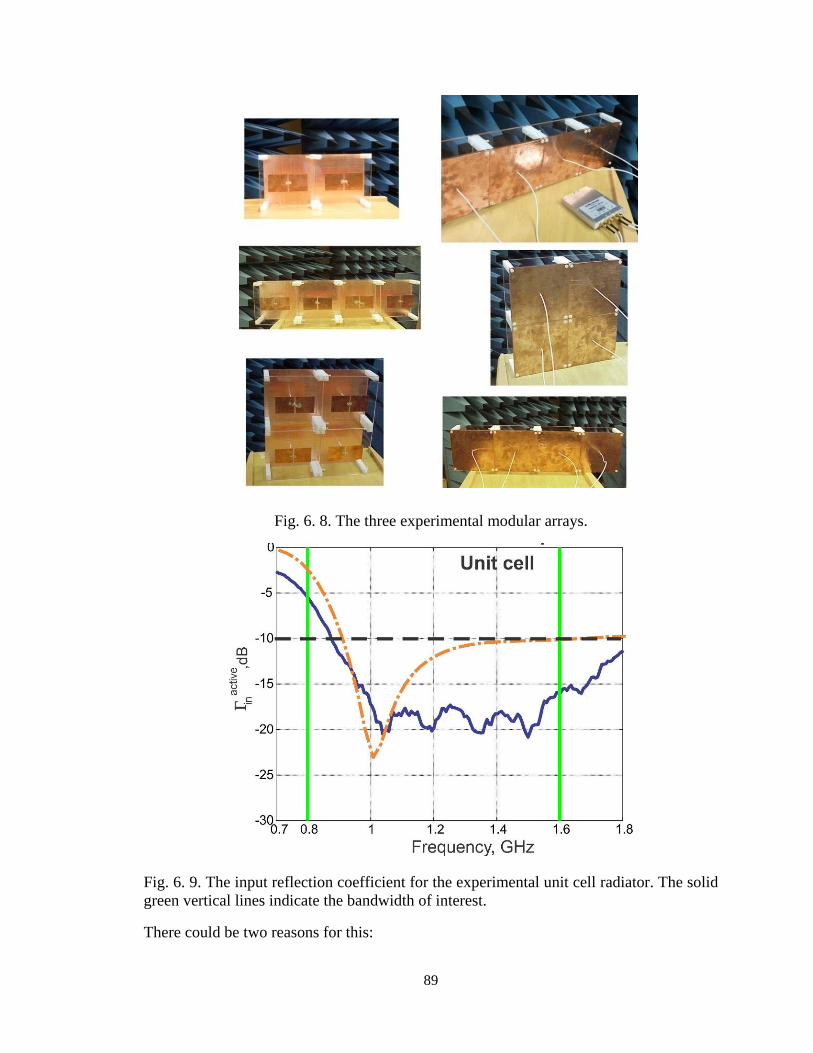
89
Fig. 6. 8. The three experimental modular arrays.
Fig. 6. 9. The input reflection coefficient for the experimental unit cell radiator. The solid green vertical lines indicate the bandwidth of interest.
There could be two reasons for this:
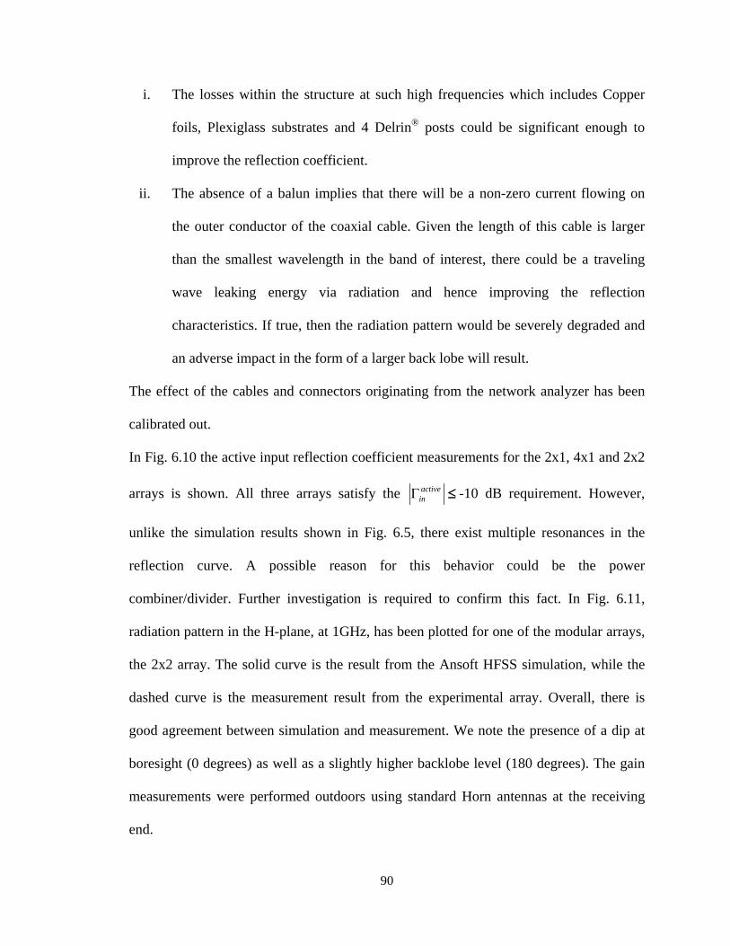
90
i. The losses within the structure at such high frequencies which includes Copper
foils, Plexiglass substrates and 4 Delrin® posts could be significant enough to
improve the reflection coefficient.
ii. The absence of a balun implies that there will be a non-zero current flowing on
the outer conductor of the coaxial cable. Given the length of this cable is larger
than the smallest wavelength in the band of interest, there could be a traveling
wave leaking energy via radiation and hence improving the reflection
characteristics. If true, then the radiation pattern would be severely degraded and
an adverse impact in the form of a larger back lobe will result.
The effect of the cables and connectors originating from the network analyzer has been
calibrated out.
In Fig. 6.10 the active input reflection coefficient measurements for the 2x1, 4x1 and 2x2
arrays is shown. All three arrays satisfy the ≤activeinΓ -10 dB requirement. However,
unlike the simulation results shown in Fig. 6.5, there exist multiple resonances in the
reflection curve. A possible reason for this behavior could be the power
combiner/divider. Further investigation is required to confirm this fact. In Fig. 6.11,
radiation pattern in the H-plane, at 1GHz, has been plotted for one of the modular arrays,
the 2x2 array. The solid curve is the result from the Ansoft HFSS simulation, while the
dashed curve is the measurement result from the experimental array. Overall, there is
good agreement between simulation and measurement. We note the presence of a dip at
boresight (0 degrees) as well as a slightly higher backlobe level (180 degrees). The gain
measurements were performed outdoors using standard Horn antennas at the receiving
end.

91
Fig. 6. 10. The active input reflection coefficient obtained from the experimental 2x1, 4x1 and 2x2 arrays. The solid green vertical lines indicate the bandwidth of interest.

92
Fig. 6. 11. H-plane radiation pattern for 2 x 2 modular array at 1 GHz. The solid blue curve is the simulation result from HFSS, while the dashed blue curve is the experimental result.

93
Chapter 7. Conclusion
This thesis addressed the topic of impedance matching of antenna radiators and in
particular the problem of broadband impedance matching. The two approaches to
impedance matching were identified, namely the distributed impedance matching
techniques and the lumped element approach. The work described in this thesis has made
original contributions to both approaches in the form of:
I. Wideband impedance matching of non-resonant dipole/monopole antennas using
the lumped element techniques
II. Modular array design of small arrays of resonant dipoles using the distributed
impedance matching techniques.
The specific contributions to each will now be outlined in the next two sections.
7.1 Thesis contributions using lumped element techniques
1) The thesis proposes a new technique for impedance matching of short non-
resonant dipole-like antennas. Instead of constructing network topology from the
particular antenna impedance data, we propose to use a simple network of one
fixed topology for all dipole-like antennas. This network is the narrowband L-
section cascaded with the high-pass T-section.
2) Matching with the network proposed in this thesis results in a performance close
to the theoretical limit on impedance matching confirmed by Bode-Fano theory.
3) Matching with the network proposed in this thesis results in a near identical
performance compared to advanced matching techniques such as the Carlin's

94
equalizer. More importantly, the network proposed in this thesis is simpler to
design and would occupy lesser area on a PCB since there are no transformers.
4) An upper bound on the maximum achievable theoretical transducer gain as a
function of dipole/monopole geometry, center frequency and bandwidth sought
has been derived.
5) Experimentally validated the theoretical and numerical simulation predictions for
a blade monopole on a 1 m x 1 m and a 75 cm x 75 cm ground plane.
6) A direct global numerical search routine for finding the optimum reflective
equalizer components written in MATLAB ©.
7.2 Thesis contributions using distributed matching techniques
1) This thesis introduces the concept of modular array design using the canonic
planar resonant dipole. The unique aspect of this approach is we seek a single
optimum unit cell radiator which will satisfy different array configurations and
yet maintain good impedance bandwidth as well as possess stable gain variation
over the bandwidth of interest.
2) We establish the need to eschew infinite array simulation models in the design of
modular arrays, by showing that the identical optimized unit cell for a 2x1, 4x1
and 2x2 array with at least an octave bandwidth, yields less than 25 % fractional
bandwidth in an infinite array.
3) Using a optimization approach and full wave modeling technique, we have found
a solution for the unit cell radiator that satisfies the VSWR of 2:1 over a
bandwidth of 2:1 and upto 3dB local directive gain variation in the band of
interest, for three array configurations 2x1, 4x1, and 2x2 arrays.

95
4) Experimentally verified the impedance bandwidth performance of the three
modular array configurations mentioned in 2, and 3.
7.3 Future research directions
The scope for further research in each area will be now outlined
Lumped element techniques for wideband matching of non-resonant antenna radiators –
1) Investigate the phase characteristics of the proposed 5 element equalizer
2) Digital tuning could pave the way for adaptive reflective equalizers. Dynamic
equalization would allow for antenna response reconfigurability.
3) Optimize the noise performance of such networks
Distributed matching techniques for Modular arrays –
1) Gain measurements have to be done to confirm the broadside array gain behavior.
2) Extend the search for the optimum unit cell radiator to other configurations such
as 3x1, 4x2, and 4x4 arrays.
3) Related to 2, answer the fundamental question of whether a solution exists for
larger configurations and what is the limit on size beyond which no solution
exists.
4) Arrays of small sizes such as the ones proposed in this thesis suffer from the finite
ground plane size edge effects. Novel ground plane shaping strategies could be
investigated to negate such effects.
5) Explore modular array design for different unit cell radiators such as the
microstrip patches.

96

97
Appendix A – Impedance Matching of Small Dipole and Loop Antennas for Wideband RFID Operation
I. INTRODUCTION
The shrinking size of radio equipment coupled with increasingly complex signal
structures has resulted in the need for reduction in antenna size and the demand for wider
bandwidths. In RFID based systems, we typically encounter electrically small antennas.
While the scope of RFID technology has been well defined in the realm of supply chain
management, yet more novel applications are being researched in areas such as mobile
healthcare services and surveillance [73], [74], near-field communication among wireless
mobile devices [75], and distributed sensor networks[76], [77]. Several practical
approaches are provided in [73], [78]-[80], for the design of RFID antennas while in [81]
the efficiency of such small antennas is discussed. However, these designs provide
fractional bandwidths of lesser than 20%.
To achieve wideband operation, impedance matching of the antenna to the source/load
has to be done. Impedance matching techniques such as the standard L, T, and Π
networks which comprise of either reactive lumped elements or sections of transmission
lines using stubs, belong in the narrowband matching category [27],[28].
In this investigation we have attempted to do wideband impedance matching i.e., higher
than 20% fractional bandwidth, of electrically small dipole, and loop antennas using
lumped components. The method we have used bypasses both the pure analytical [16]-
[19], and the RFT numerical approach [23]-[26], [82]-[84]. Instead, we introduce the
equalizer topology upfront and subsequently employ a direct numerical optimization

98
technique to find the component values. In order to get an idea regarding the maximum
achievable gain for the matching network the Bode-Fano criterion will be used and this
analysis will be presented in section II. Section III describes the two equalizer circuits to
be used for the dipole and the loop respectively. An upper bound on the system efficiency
for will be discussed in Section IV. Section V will present the simulation results. Finally,
section VI provides the conclusions.
II. THEORETICAL LIMIT ON WIDEBAND IMPEDANCE MATCHING OF
SMALL DIPOLE AND LOOP
A. Antenna Impedance Model – Small Dipole, Small Circular Loop
The input impedance, of a small dipole, dpZ can be expressed as dpdpdp jXRZ += [32],
where, the radiation resistance is given by
( ) ∀= 2220 λπ Adp lR 1050 λλ ≤≤ Al (1)
and, the input reactance
( )[ ]( )2tan
12ln120A
Adp kl
alX −−= . (2)
In (1), (2), Al is the dipole length, a, is the dipole radius, and λπ2=k is the
wavenumber. The small dipole condition can be expressed in the frequency domain as
2.004.0 ≤< resc ff , where, Ares lcf 20≡ is the resonant frequency of a half wave
resonant ideal dipole, 0c is the speed of light and cf is the center frequency. The input
impedance is predominantly capacitive. In the case of a monopole over an infinite ground
plane the impedance Zdp is halved.

99
For the small circular loop, the impedance, lpZ can be expressed as lplplp jXRZ += [32],
where, the loop radiation resistance can be expressed as,
( ) ∀= 4220 λπ CRlp 10λ<C (3)
and the loop inductance is,
( )[ ]28ln0 −= brrL µ (4)
In (3), (4) r is the radius of the loop, b the radius of the conductor and rC π2= , is the
circumference of the loop. The internal reactance of the loop conductor has been ignored.
The thickness of the conductor is chosen by using ( )brπρ 2ln2= , such that
9<ρ represents moderately thick loops [32]. Since we consider the small circular loop,
in the frequency domain the condition to be met is, 1.0<resc ff , where Ccfres 0≡ , is
the resonant frequency of the electrically large loop, and cf is the center frequency. The
input impedance for the small circular loop is predominantly inductive.
B. Wideband Impedance Matching - The Reflective Equalizer
The reactive matching network and the Thévenin equivalent circuit when viewed from
the antenna is shown in Fig. A.1a and A.1b, respectively [23]. This network can be
considered to be a reflective equalizer which always reflects a portion of the power back
to the generator over the bandwidth of interest. The transducer gain is [23],

100
Fig. A. 1. Matching network: a) reactive matching network representation. b) Thévenin-equivalent circuit.
.)(1)()()()(4)( 2
22 ω
ωωωω
ω Γ−=+
=TA
T
ZZRRT (5)
The problem can therefore be summarized as one of maximizing the minimum gain over
a specified wide bandwidth B [23], [26].
C. Bode-Fano Bandwidth Limit
We can approximate the antenna model for these two antennas as series RC and RL
networks respectively. The Bode-Fano relations pertaining to the small dipole and the
small loop in terms of the reflection coefficient )(ωΓ at the input to the matching
network is expressed as [28],
.)(
1ln
)(1ln1
0
02
LRdLoopSmall
RCdDipoleSmall
πωω
πωωω
<
Γ⇒
<
Γ⇒
∫
∫∞
∞
(6)

101
These integral relations will be solved over a rectangular band-pass frequency window of
bandwidth B and centered at cf . The transducer gain within this window is T = T0 and T
= 0 outside of it.
D. Arbitrary Fractional Bandwidth and Transducer Gain
The first case we will consider is the small dipole. To reference Fig. 1, ZA=Zdp is the load
impedance under consideration. From (2), we extract the capacitance of the small dipole.
Let us define, 2Aklz = , which is restricted to 10/50 ππ ≤< z . Therefore, we can rewrite
(2) as,
( )[ ]z
alX Adp
12ln120 −−= . (7)
The capacitance, C is then found to be from (7),
( )[ ]( ) 112ln480 −−= alfC Ares . (8)
Solving the Bode-Fano integral for the small dipole from (6) by using (8), and by
defining the fractional bandwidth as cfBB = , we arrive at,
( ) ( )( )( )
−
−−−<
12ln2441(
exp1 3
234
0 alfBBf
TAres
cdp π . (9)
Hence, given the desired fractional bandwidth from a small dipole, the maximum
achievable transducer gain ( )dpT0 over this bandwidth can be predicted by (9).
In a similar approach, solving the integral relation for the small circular loop with ZA=Zlp
and using (3) and (4) in (6), we get,

102
( )( ) .28ln
20exp1
04
32)(
0
−
−−<brrfB
fT
res
Clp
µπ
(10)
which represents the upper limit on transducer gain for the small circular loop, over a
desired fractional bandwidth.
III. MATCHING CIRCUITS
Conventional impedance matching technique such as the 2 element L or C-section match
for a given load is narrowband since the match occurs exactly only at a single frequency.
To increase the bandwidths of these sections we suggest a high-pass network be cascaded
to the 2-element matching sections as shown in Fig. A.2 and A.3. The Thévenin
impedance for the equalizer as seen from the antenna for both, the small dipole and loop
circuits is given as,
( )( ) 354
541
2
2 11
1,
sCsCRsLsCRsL
ZsLZsL
ZsLZ
g
gg
g
gdpT +
++
+=+
+=
(11)
( )( )
( )( ) 34
4
12
2 1,111
sCsLRsLR
ZsCZsC
ZsCZ
g
gg
g
glpT +
+=+
+= (12)
where s=jω. The upper limit in (9), (10) will be used for the sake of comparison.
Fig. A. 2. Extension of the L-tuning network for certain fixed values of L1, L2 by the T- section for small dipole.

103
Fig. A. 3. Extension of the L-tuning network for certain fixed values of C1, C2 by a high pass section for small loop.
IV. UPPER BOUND ON SYSTEM EFFICIENCY
The upper bound on efficiency for a system comprising an electrically small antenna with
a corresponding impedance matching network, as shown in Fig. A.2 and Fig. A.3, is
sought. Let Rin(ω), be the input resistance at the antenna feed point. The input resistance
can be expressed in terms of the radiation resistance, Rr(ω), and the loss resistance,
Rloss(ω), as,
)()()( ωωω lossrin RRR += . (13)
In [85] it is suggested that the system efficiency of the antenna-matching network
combination would be maximum if the network has no storage elements that store energy
of the same form as the antenna. Thus, the system efficiency sη , has been defined as,
QQa
amas
′+==
)(1
)()()()(
ωωη
ωηωηωη (14)
where, mη , is the efficiency of the matching network, aη is the efficiency of the antenna,
Q′ is the Quality factor of the network elements that store energy in the form opposite to
that of the antenna, and aQ is the antenna quality factor. We can therefore deduce that the

104
simple L - section or the C - section matching network comprising of only inductors or
capacitors, as shown in Fig. A.2 and Fig. A.3, for a dipole or loop antenna respectively,
would achieve the highest possible system efficiency. The antenna Quality factor, Qa is
approximated as,
( ) ( )( )cin
cCa R
XQ
ωωωω
ωω=
=== . (15)
Using (13) we can rewrite (15) as,
( ) ( )( ) ( )closscr
cCa RR
XQ
ωωωωωω
ωω=+=
=== . (16)
We can use this approximation since we are clearly below the first resonance of the
antenna. Since, losses in antenna structure have been assumed to be small, we set the
term Rloss(ω) ≈ 0 to obtain,
( ) ( )( )cr
cCa R
XQ
ωωωω
ωω=
=== . (17)
The efficiency of the antenna is defined in the standard way as follows,
( )( ) ( )ωω
ωη
lossr
ra RR
R+
= (18)
Since the loss resistance is assumed to be negligible in the antenna structure, the
efficiency of the antenna aη ≈1. Therefore, a simple expression for the upper bound on
system efficiency for the case of an electrically small antenna in combination with a
matching network is obtained from (14) as
105
QQa
s
′+
=)(
1
1)(ω
ωη (19)
V. NUMERICAL SIMULATION AND RESULTS
A. Simulation Setup
The set of tested antenna parameters for small dipole and loop are shown in Table A.1.
The resonant frequency of both the small dipole and circular loop was chosen as 1 GHz.
For the small dipole, d refers to the diameter. The matching network components are
obtained through optimization. This is done by using a direct global numerical search in
the space of circuit parameters. The minimum gain achieved over the band is calculated
[23] for every circuit parameter set and only the ones that satisfy the ±25% gain variation
criterion are retained.
Table A. 1. SIMULATION PARAMETERS
Parameter Small Dipole Small Loop
Geometry 10=dlA 10=ρ
B 0.5 0.5
resC ff / [0.05:0.2] [0.05:0.1]
B. Realized Gain – Small Dipole, 5.0,10 == Bdl A
Fig. A. 4 shows the realized average generator gain for the small dipole. The solid line is
the upper limit derived from Bode-Fano theory in Eq. (9) and the realized values are
shown by squares. The network performs rather closely to the upper limit T0 if we

106
consider the average gain over the band. The deviation from the upper limit is 33%. The
component values for resc ff = 0.15 are, [L1, L2, C3, L4, C5] = [762.8nH, 175.8nH,
49.6pF, 837.4nH, 10.5pF].
C. Realized Gain – Small Circular Loop, ρ=10, 5.0=B
In Fig. A.5 the realized average generator gains for a small circular loop are plotted for
different center frequencies. As before the solid line corresponds to the theoretical upper
limit derived from the Bode-Fano criterion in Eq. (10). The small loop requires one less
component in the matching network as compared to the small dipole. The generator gain
approaches this upper limit, with the average deviation between the two being 34%. The
component values for resc ff = 0.0875 are, [C1, C2, C3, L4] = [23.1pF, 94.08pF,
571.5pF, 40.7nH].
D. System Efficiency – Small Dipole and Small Loop
The upper bound on system efficiency for the small dipole and loop has been calculated
at various center frequencies using Eq. (19). For the case of the small dipole, the L-
section matching network uses two inductors, L1 and L2. The Q factor for these
components is assumed to be 55. Similarly the C-section matching network for the small
loop uses two capacitors C1 and C2 with Q-factor of 1000. Fig. A.6. shows the upper
bound on system efficiency for the small dipole.

107
Fig. A. 4. Realized average generator gain ( )dpT0 (squares) for a small dipole with 10=dlA .
Fig. A. 5. Realized average generator gain ( )lpT0 (squares) for a loop with ρ=10.

108
Fig. A. 6. Upper bound on system efficiency for the small dipole with lA/d=10.
Similarly, Fig. A.7 shows the upper bound on system efficiency for a small loop.
Fig. A. 7. Upper bound on system efficiency for the small loop with ρ=10
VI. CONCLUSION
In this study we have presented a wideband impedance matching approach for the
electrically small dipole and loop antennas. The Bode-Fano theoretical limit for
maximum transducer gain has been derived and used for comparison of the proposed

109
networks. It has been shown that the average deviation between the realized gain and the
theoretical upper limit is approximately 33% for both types of antennas. In doing so a
gain variation criterion of ±25% over the band of interest has been applied while
calculating the transducer gain. The system efficiency for the small antenna in
combination with the matching network was discussed; an upper bound was derived and
plotted at different center frequencies.
It is observed that the realized generator gain and the efficiencies are low. This is
primarily because of the low value of radiation resistance of the small antenna. Even so,
the small loop is capable of higher efficiency than the small dipole. Modifying the
antenna structure to increase the radiation resistance would potentially alleviate this issue
and increase generator gain. Of course, it is then possible that the antenna efficiency
might decrease.

110
Appendix B – ADS analysis of a monopole with reflective equalizer
I. MODELING THE WIDEBAND IMPEDANCE MATCHING OF MONOPOLE
ANTENNA IN AGILENT - ADS
Goal: To analyze the behavior of the lumped component based equalizer, designed to do
wideband impedance matching for a 11.5 cm monopole antenna over ground plane, by
simulating it in Agilent ADS.
Solution
Our goal is to build a model of the system comprising of the wideband matching network
and the monopole antenna to effectively mirror the real system.
:
Fig. B. 1. ADS simulation set up.
In Fig. B.1 and Fig. B.2, the S-parameter simulation set up is shown in ADS along with
the substrate parameters corresponding to the FR-4 board that was used as substrate for
the wideband matching network PCB. The results of this simulation are seen in Fig. B.3.

111
Fig. B. 2. ADS simulation set up of the wideband reflective equalizer.
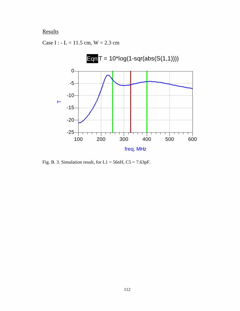
112
Case I : - L = 11.5 cm, W = 2.3 cm
Results
Eqn T = 10*log(1-sqr(abs(S(1,1))))
200 300 400 500100 600
-20
-15
-10
-5
-25
0
freq, MHz
T
Fig. B. 3. Simulation result, for L1 = 56nH, C5 = 7.63pF.

113
Appendix C – Comparison of input impedance of the electrically small dipole and loop antennas using analytical, Method of Moments (MoM) and Ansoft HFSS solutions
The input resistance R of an electrically small (this means small compared to the
wavelength at the center frequency) dipole antenna has the form
2
20
2
20
6
~
32
λπη
λπη AA llR == (1)
where Al~ is the antenna half length and fc /0=λ is the wavelength.
The blade dipole antenna has total length Al =150mm and the width of 5 mm, 15mm
respectively
Table C. 1. Input resistance of a small dipole antenna (Ω ), 30=tl .
Frequency 20 MHz
100/λ
40 MHz
50/λ
100 MHz
20/λ
200 MHz
10/λ
400 MHz
5/λ
R- Analytical 1.97 e-2
7.9 e-2 4.94 e-1 1.97 7.90
R-MoM, t = 5mm 1.449 e-2 5.8 e-2 3.65e-1 1.497 6.63
R-FEM, t = 5mm
PML, 1000x1000x1000mm
15 passes, 1GHz
4.15 e-2 7.8 e-2 3.9 e-1 1.56 6.94
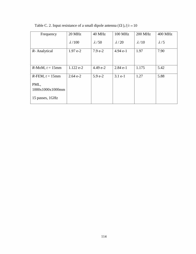
114
Table C. 2. Input resistance of a small dipole antenna (Ω ), 10=tl
Frequency 20 MHz
100/λ
40 MHz
50/λ
100 MHz
20/λ
200 MHz
10/λ
400 MHz
5/λ
R- Analytical 1.97 e-2
7.9 e-2 4.94 e-1 1.97 7.90
R-MoM, t = 15mm 1.122 e-2 4.49 e-2 2.84 e-1 1.175 5.42
R-FEM, t = 15mm
PML, 1000x1000x1000mm
15 passes, 1GHz
2.64 e-2 5.9 e-2 3.1 e-1 1.27 5.88

115
The input reactance X of an electrically small (this means small compared to the
wavelength at the center frequency) dipole antenna has the form
−−=
A
A
lalX λ
πη
12
ln20 (2)
4/ta = where a is the (equivalent) wire radius and t is the (equivalent) blade width.
Table C. 3. Input reactance of a small dipole antenna (Ω ), 30=tl .
Frequency 20 MHz
100/λ
40 MHz
50/λ
100 MHz
20/λ
200 MHz
10/λ
400 MHz
5/λ
X- Analytical -11807.45 -5897.89 -2342.78 -1141.96 -510.61
X-MoM, t = 5 mm -10811.13 -5400.21 -2145.05 -1045.33 -465.36
X-FEM, t = 5 mm
PML 1000x1000x1000mm
15 passes, 1 GHz
-10717.6 -5353.37 -2126.02 -1035.27 -459.33
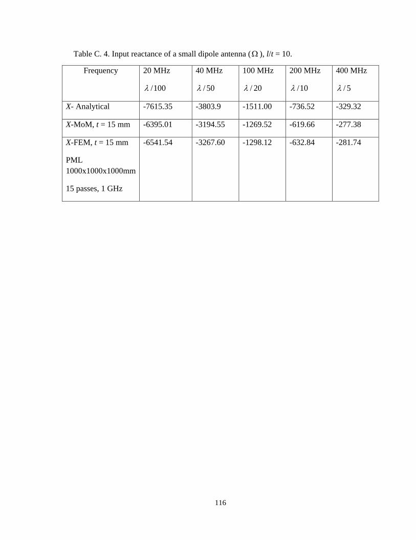
116
Table C. 4. Input reactance of a small dipole antenna (Ω ), l/t = 10.
Frequency 20 MHz
100/λ
40 MHz
50/λ
100 MHz
20/λ
200 MHz
10/λ
400 MHz
5/λ
X- Analytical -7615.35 -3803.9 -1511.00 -736.52 -329.32
X-MoM, t = 15 mm -6395.01 -3194.55 -1269.52 -619.66 -277.38
X-FEM, t = 15 mm
PML 1000x1000x1000mm
15 passes, 1 GHz
-6541.54 -3267.60 -1298.12 -632.84 -281.74
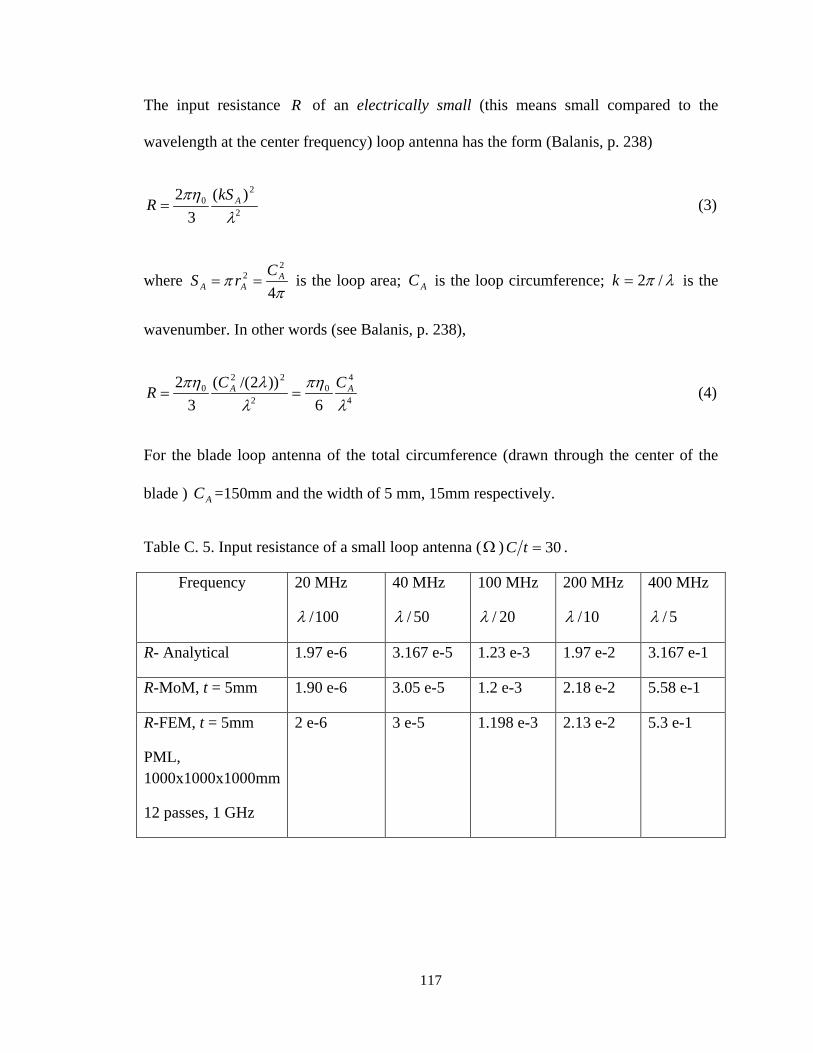
117
The input resistance R of an electrically small (this means small compared to the
wavelength at the center frequency) loop antenna has the form (Balanis, p. 238)
2
20 )(
32
λπη AkSR = (3)
where π
π4
22 AAA
CrS == is the loop area; AC is the loop circumference; λπ /2=k is the
wavenumber. In other words (see Balanis, p. 238),
4
40
2
220
6))2/((
32
λπη
λλπη AA CCR == (4)
For the blade loop antenna of the total circumference (drawn through the center of the
blade ) AC =150mm and the width of 5 mm, 15mm respectively.
Table C. 5. Input resistance of a small loop antenna (Ω ) 30=tC .
Frequency 20 MHz
100/λ
40 MHz
50/λ
100 MHz
20/λ
200 MHz
10/λ
400 MHz
5/λ
R- Analytical 1.97 e-6 3.167 e-5 1.23 e-3 1.97 e-2 3.167 e-1
R-MoM, t = 5mm 1.90 e-6 3.05 e-5 1.2 e-3 2.18 e-2 5.58 e-1
R-FEM, t = 5mm
PML, 1000x1000x1000mm
12 passes, 1 GHz
2 e-6 3 e-5 1.198 e-3 2.13 e-2 5.3 e-1
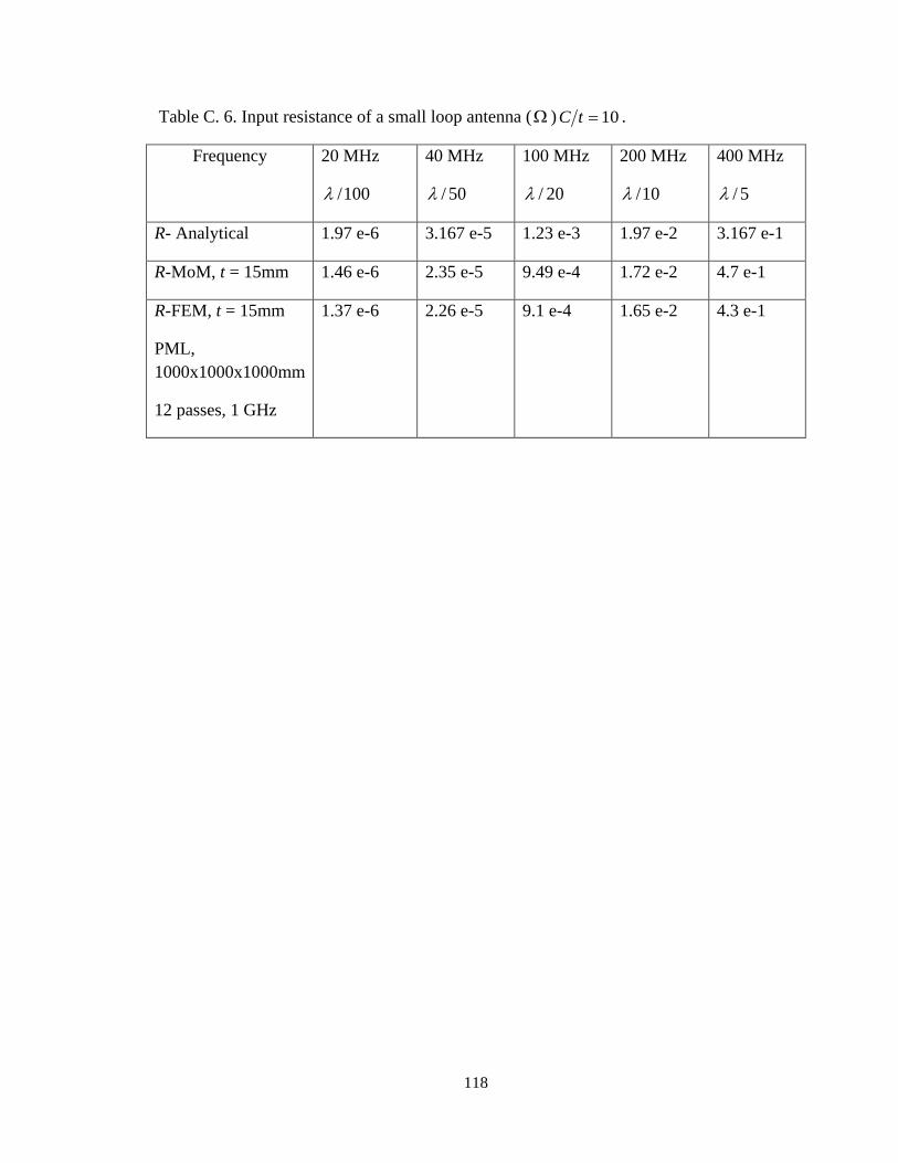
118
Table C. 6. Input resistance of a small loop antenna (Ω ) 10=tC .
Frequency 20 MHz
100/λ
40 MHz
50/λ
100 MHz
20/λ
200 MHz
10/λ
400 MHz
5/λ
R- Analytical 1.97 e-6 3.167 e-5 1.23 e-3 1.97 e-2 3.167 e-1
R-MoM, t = 15mm 1.46 e-6 2.35 e-5 9.49 e-4 1.72 e-2 4.7 e-1
R-FEM, t = 15mm
PML, 1000x1000x1000mm
12 passes, 1 GHz
1.37 e-6 2.26 e-5 9.1 e-4 1.65 e-2 4.3 e-1
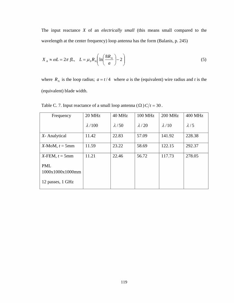
119
The input reactance X of an electrically small (this means small compared to the
wavelength at the center frequency) loop antenna has the form (Balanis, p. 245)
−
==≈ 28ln,2 0 a
RRLfLLX AAA µπω (5)
where AR is the loop radius; 4/ta = where a is the (equivalent) wire radius and t is the
(equivalent) blade width.
Table C. 7. Input reactance of a small loop antenna (Ω ) 30=tC .
Frequency 20 MHz
100/λ
40 MHz
50/λ
100 MHz
20/λ
200 MHz
10/λ
400 MHz
5/λ
X- Analytical 11.42 22.83 57.09 141.92 228.38
X-MoM, t = 5mm 11.59 23.22 58.69 122.15 292.37
X-FEM, t = 5mm
PML 1000x1000x1000mm
12 passes, 1 GHz
11.21 22.46 56.72 117.73 278.05
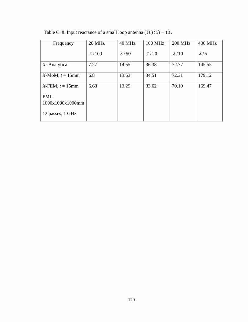
120
Table C. 8. Input reactance of a small loop antenna (Ω ) 10=tC .
Frequency 20 MHz
100/λ
40 MHz
50/λ
100 MHz
20/λ
200 MHz
10/λ
400 MHz
5/λ
X- Analytical 7.27 14.55 36.38 72.77 145.55
X-MoM, t = 15mm 6.8 13.63 34.51 72.31 179.12
X-FEM, t = 15mm
PML 1000x1000x1000mm
12 passes, 1 GHz
6.63 13.29 33.62 70.10 169.47
121
Appendix D – Example design of single and dual band matching networks
I. LLNL – HANDSET MATCHING NETWORK SPECIFICATIONS
Handset Specifications
Dimensions: - W X D X H = 7cm X 5cm X 15cm
: -
Frequency: - 250MHz – 400MHz
Bandwidth: - 150MHz
Antenna specifications
Type: - Blade
: -
Length: - 11.5cm
Width: - 2.3cm
Thickness: - 0.25mm
II. FULL WAVE MODELING
These specifications were used to model the structure in ANSOFT – HFSS. The entire
structure consisting of the blade and the handset is considered to be the antenna. A
lumped port feed with a feed gap of 1mm was used for the excitation source. The
radiation boundary was located at 0.325λ from the structure on all sides. Fig. D.1 shows
the final model built using HFSS. The blade and the handset are modeled as Perfect
electric conductors (PEC). The blade and the corresponding feed are located off of the
edge of the top surface on the handset. A total of 15 passes were used for mesh
generation which resulted in about 16,500 tetrahedra being generated.

122
Fig. D. 1. Handset model in ANSOFT- HFSS.
III. MATCHING NETWORK
The device is being operated below the first resonance of the blade-handset structure. The
input impedance of this structure is shown in Fig. D.2 over the operating bandwidth of
150MHz.
Fig. D. 2. Input impedance of blade-handset antenna.

123
As observed, the antenna impedance is predominantly capacitive with a resistive part that
varies from approximately 5 - 25Ω across 250MHz – 400MHz. The maximum directivity
of this antenna is close to that of an ideal dipole in free space (~2.2dB) and is shown in
Fig. D.3. There is a slight tilt observed in the pattern wherein the null is no longer exactly
at zenith. This structure is essentially an offset center fed dipole, wherein the the handset
body is also contributing to the radiation. Since, the gain is the important parameter of
interest, we must attempt to make this antenna efficient as well as reduce the mismatch
loss. Assuming a highly efficient structure, we focus on reducing the mismatch losses
that would occur due to this antenna being driven by a purely resistive 50Ω source.
Fig. D. 3. Directivity of the blade-handset antenna.
Our approach is to design a 5 element matching network built entirely out of reactive
components. We extend the traditional L-section matching used for narrowband
impedance matching and cascade a highpass T-section comprising of two series

124
capacitors and a shunt inductor as shown in Fig. D.4. A direct search based technique is
used to obtain the component values in the matching network.
Fig. D. 4. Extension of the L-tuning section for fixed values of L1, L2 by the T-section.
Results
A 5 element matching network was obtained from the optimization procedure and the
component values are shown in Table D.1.
Table D. 1. Circuit parameters for the matching network used to match the blade-handset antenna to resistive 50Ω source.
COMPONENT VALUE (nH/pF) L1 47.24 L2 31.49 C3 16.12 L4 466.66 C5 13.33
The transducer gain obtained across the operating bandwidth due to the matching
network is shown in Fig. D.5. The average transducer gain can be translated to an average
return loss as follows, 22 )(1)( ωω Γ−=T where T is the transducer gain and Γ is the
reflection coefficient. Thus, the avg. gain of 0.42871 translates to approximately 2.43dB
average return loss across the 150MHz bandwidth. This is an improvement and we can
compare it to the return loss of the blade-handset antenna without the matching network

125
which is shown in Fig. D.6. As seen in this plot, the S11 varies from about 0dB to roughly
-3dB at the higher end of the frequency range.
Fig. D. 5. Average transducer gain.
Fig. D. 6. S11 of blade-handset antenna without matching network.
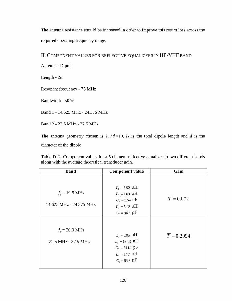
126
The antenna resistance should be increased in order to improve this return loss across the
required operating frequency range.
II. COMPONENT VALUES FOR REFLECTIVE EQUALIZERS IN HF-VHF BAND
Antenna - Dipole
Length - 2m
Resonant frequency - 75 MHz
Bandwidth - 50 %
Band 1 - 14.625 MHz - 24.375 MHz
Band 2 - 22.5 MHz - 37.5 MHz
The antenna geometry chosen is dlA / =10, lA is the total dipole length and d is the
diameter of the dipole
Table D. 2. Component values for a 5 element reflective equalizer in two different bands along with the average theoretical transducer gain.
Band Component value Gain
cf = 19.5 MHz
14.625 MHz - 24.375 MHz
92.21 =L µH 09.12 =L µH 54.33 =C nF 43.54 =L µH
8.945 =C pF
072.0=T
cf = 30.0 MHz 22.5 MHz - 37.5 MHz
05.11 =L µH
9.6342 =L nH 1.3443 =C pF
77.14 =L µH 9.885 =C pF
2094.0=T
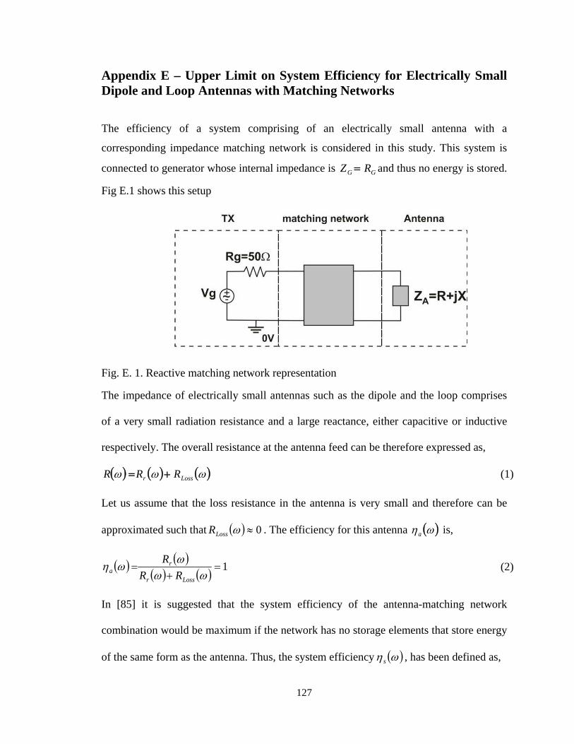
127
Appendix E – Upper Limit on System Efficiency for Electrically Small Dipole and Loop Antennas with Matching Networks
The efficiency of a system comprising of an electrically small antenna with a
corresponding impedance matching network is considered in this study. This system is
connected to generator whose internal impedance is GG RZ = and thus no energy is stored.
Fig E.1 shows this setup
Fig. E. 1. Reactive matching network representation
The impedance of electrically small antennas such as the dipole and the loop comprises
of a very small radiation resistance and a large reactance, either capacitive or inductive
respectively. The overall resistance at the antenna feed can be therefore expressed as,
( ) ( ) ( )ωωω Lossr RRR += (1)
Let us assume that the loss resistance in the antenna is very small and therefore can be
approximated such that ( ) 0≈ωLossR . The efficiency for this antenna ( )ωηa is,
( ) ( )( ) ( ) 1=
+=
ωωω
ωηLossr
ra RR
R (2)
In [85] it is suggested that the system efficiency of the antenna-matching network
combination would be maximum if the network has no storage elements that store energy
of the same form as the antenna. Thus, the system efficiency ( )ωη s , has been defined as,

128
( ) ( )
QQa
amas
′+==
)(1 ωωη
ηηωη (3)
where, mη , is the efficiency of the matching network, Q′ is the Quality factor of the
network elements that store energy in the form opposite to that of the antenna, and aQ is
the antenna Quality factor. We can therefore deduce that the L section matching network
comprising of all inductors or all capacitors, as shown in Fig. E.2 for a dipole or loop
antenna respectively would achieve the highest possible system efficiency.
Fig. E. 2. L - Section matching network.
The antenna Quality factor, Qa is approximated as,
( ) ( )( )
( )( ) ( )closscr
c
c
cCa RR
XRX
Qωωωω
ωωωωωω
ωω=+=
==
==
== (4)
We can use this approximation since we are clearly below the first resonance of the
antenna. Since, losses in antenna structure have been assumed to be small, we get,
( ) ( )( )cr
cCa R
XQ
ωωωω
ωω==
== (5)
From [32], the radiation resistance of a small dipole is given to be,
( ) ∀= 2220 λπ Adp lR 1050 λλ ≤≤ Al (6)

129
and reactance can be derived as,
−
−=
2
12ln120
A
A
dp kla
l
X (7)
In Eq. (6), lA is the dipole length, a, is the dipole radius, and λπ2=k is the
wavenumber.. In the case of a strip or blade dipole of width t, the equivalent radius is
4taeq = [32]. The small dipole condition can be expressed in the frequency domain
as 2.004.0 ≤< resc ff , where, Ares lcf 20≡ is the resonant frequency of a half wave
resonant ideal dipole, 0c is the speed of light and cf is the center frequency. Note that the
expression for reactance holds only within the dimension limits specified in Eq. (6).
Similarly, for the circular loop, we have
( ) ∀= 4220 λπ CRlp 10λ<C (8)
and the loop inductance is,
( )[ ]28ln0 −= brrL µ (9)

130
RESULTS
We consider the following parameters for our numerical simulation.
Case I: Electrically small dipole
Table E. 1. Simulation Parameters.
PARAMETER VALUE
resf 1 GHz
dlA [5 10 50]
Q L1,L2 55
resc ff [0.05:0.2]
Fig.E. 3. Upper bound on achievable system efficiency for small dipole.

131
Case II: Short dipole
Considering a short dipole below the first resonance, such that the model for the
impedance of the dipole is changed to,
32
32
6031967938008261744560)(613115396303246747870)(
)(cot12
ln120)(
z. z.z - ..-zXz.z.z ..-zR
zXza
ljzRZ AA
++≈
+++≈
−
−−=
(10)
Table E. 2. Simulation parameters
PARAMETER VALUE
resf 1 GHz
dlA [5 10 50]
Q L1,L2 55
resc ff [0.05:0.5]
Fig. E. 4. The achievable system efficiency for short dipole.

132
Case III: Electrically small circular loop
Table E. 3. Simulation Parameters.
PARAMETER VALUE
resf 1 GHz
Ω(thickness factor[2]) [8 10 12]
Q C1,C2 1000
resc ff [0.05:0.1]
Fig. E. 5. The achievable system efficiency for an electrically small loop.
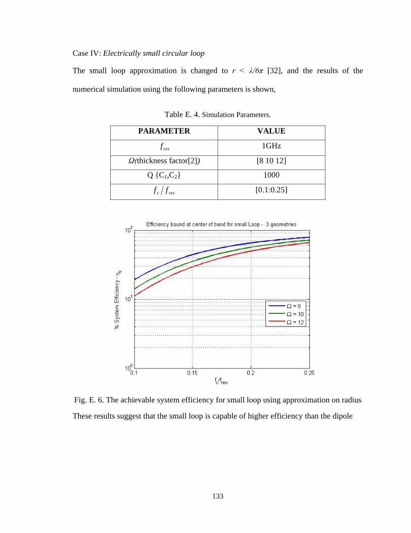
133
Case IV: Electrically small circular loop
The small loop approximation is changed to r < λ/6π [32], and the results of the
numerical simulation using the following parameters is shown,
Table E. 4. Simulation Parameters.
PARAMETER VALUE
resf 1GHz
Ω(thickness factor[2]) [8 10 12]
Q C1,C2 1000
resc ff [0.1:0.25]
Fig. E. 6. The achievable system efficiency for small loop using approximation on radius
These results suggest that the small loop is capable of higher efficiency than the dipole

134
The predicted efficiencies are close to 80- 95% for dipole and loop, at the upper
frequencies. This can be explained by observing the Q factor of the antennas,
A look at the Q-factor approximation for dipole and loop antenna
Fig. E. 7. The dipole quality factor as a function of center frequency of operation.
Fig. E. 8. The loop quality factor as a function of center frequency of operation.
The lower antenna Q implies a better radiation mechanism and hence improved efficiency.
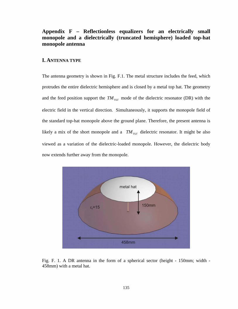
135
Appendix F – Reflectionless equalizers for an electrically small monopole and a dielectrically (truncated hemisphere) loaded top-hat monopole antenna
I. ANTENNA TYPE
The antenna geometry is shown in Fig. F.1. The metal structure includes the feed, which
protrudes the entire dielectric hemisphere and is closed by a metal top hat. The geometry
and the feed position support the δ01TM mode of the dielectric resonator (DR) with the
electric field in the vertical direction. Simultaneously, it supports the monopole field of
the standard top-hat monopole above the ground plane. Therefore, the present antenna is
likely a mix of the short monopole and a δ01TM dielectric resonator. It might be also
viewed as a variation of the dielectric-loaded monopole. However, the dielectric body
now extends further away from the monopole.
Fig. F. 1. A DR antenna in the form of a spherical sector (height - 150mm; width - 458mm) with a metal hat.

136
II. RADIATION PATTERN
The radiation pattern of the DR antenna as seen in Fig. F.2, indicates a monopole like
behavior.
Fig. F. 2. The radiation pattern of the dielectrically loaded (truncated hemisphere) top-hat monopole antenna at 110 MHz. Note, that mismatch loss is not taken into account.
III. RESONANT FREQUENCY
The antenna shown in Fig. F. 1 has an interesting performance. It does resonate at about
50 MHz as Fig. F. 3 shows. The corresponding simulations in Ansoft HFSS have been
done with a large PML box on the size of 5m×5m×5m (the PML thickness was 2.5m),
with the lowest frequency of 30 MHz, and on fine meshes with about 100,000 tetrahedra
and better. Note that the wavelength at resonant frequency of 50 MHz is 6m. Thus, the
selected PML size guarantees us the good accuracy at low frequencies up to 30 MHz.
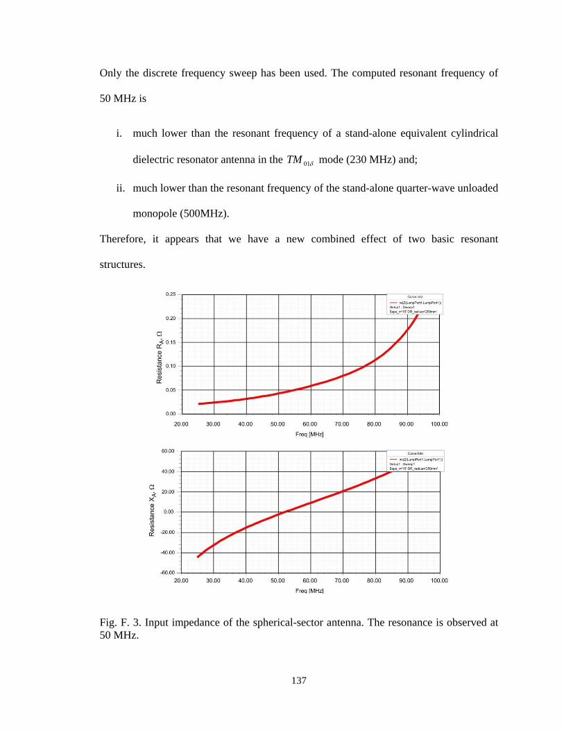
137
Only the discrete frequency sweep has been used. The computed resonant frequency of
50 MHz is
i. much lower than the resonant frequency of a stand-alone equivalent cylindrical
dielectric resonator antenna in the δ01TM mode (230 MHz) and;
ii. much lower than the resonant frequency of the stand-alone quarter-wave unloaded
monopole (500MHz).
Therefore, it appears that we have a new combined effect of two basic resonant
structures.
Fig. F. 3. Input impedance of the spherical-sector antenna. The resonance is observed at 50 MHz.
138
At the same time, the radiation resistance of the antenna in Fig. F.1 is very small, on the
order of 0.1Ω and less at the resonance. Therefore, the antenna should be matched over
the band using a dedicated lumped circuit - the equalizer.
IV. EXTRACTING MODEL PARAMETERS FOR A RESONANT ELECTRICALLY
SMALL TOP-HAT DIELECTRICALLY (TRUNCATED HEMISPHERE) LOADED
MONOPOLE ANTENNA
The LCR parameters of the series resonant circuit must be extracted for proper
impedance matching and efficient equalizer design. The input impedance of the dipole
using a series RLC circuit as the model is given by
( ) sCsLRZ 1++=ω
(1)
Here, s = jω is the complex frequency. Therefore we rewrite Eq. (1) in terms of ω shown
in Eq. (2)
( ) ( )CLjRZ ωωω 1−+=
(2)
Our goal is to extract the parameters R, L and C given the frequency dependent
impedance Z (ω). In this case, the impedance data has been obtained through simulation
of the antenna in Ansoft HFSS - see Fig. F.3. The impedance data is obtained in complex
form, i.e. Z (ω) = R + jX at N frequency points. In order to extract L and C, we consider
the following set of equations for the reactance obtained from Eq. (2),
( ) ( ) NnXC
LCZ n
n
nn 1
12
=∀=−
= ωω
ωωIm
(3)

139
If we expand this equation out we obtain
( ) NnCXLC nnn 1012 =∀=−− ωωω (4)
For each frequency point, this equation needs to be satisfied, i.e.
( )( )
( ) 01
01
01
2
222
2
112
1
=−−
=−−
=−−
NNN CXLC
CXLC
CXLC
ωωω
ωωω
ωωω
(5)
This can be written in matrix-vector notation as,
( )
( )
=
−−
−−
0
0
11
1
112
1121
CLC
X
X
N ωωω
ωωω (6)
Eq. 6 is an overdetermined matrix equation that shall be solved by SVD. It can be written
as
0
=xW (7)
This implies that the solution x belongs to the null-space of W. If W were square, we
could have computed the eigen-decomposition and this would have given us the
necessary eigenvector solution. However, here we have a tall matrix, and so we use the
SVD (Singular Value Decomposition) instead. The result of the SVD on the matrix W is
shown in Eq. (8)
VUW Σ= (8)

140
where, U and V are the matrices and the diagonal matrix Σ comprises the singular values
of W. Out of this result we need the right singular vector only, since this is the desired
solution to Eq. 7. The column vectors of V are this exactly and we choose the vector that
has all positive values and has its final entry closest to 1. The resistance value for this
model is chosen to be the average value of resistance from the simulated impedance data.
The model parameters are given below in Table 1 that follows.
Table F. 1. Model parameters of the input impedance.
R 0.07 Ω
L 83.688 pF
C 114.41 nH
The corresponding parameter approximation is given in Fig. F. 4.
Fig. F. 4. Comparison between the extracted and exact antenna parameters - see Table F.1.
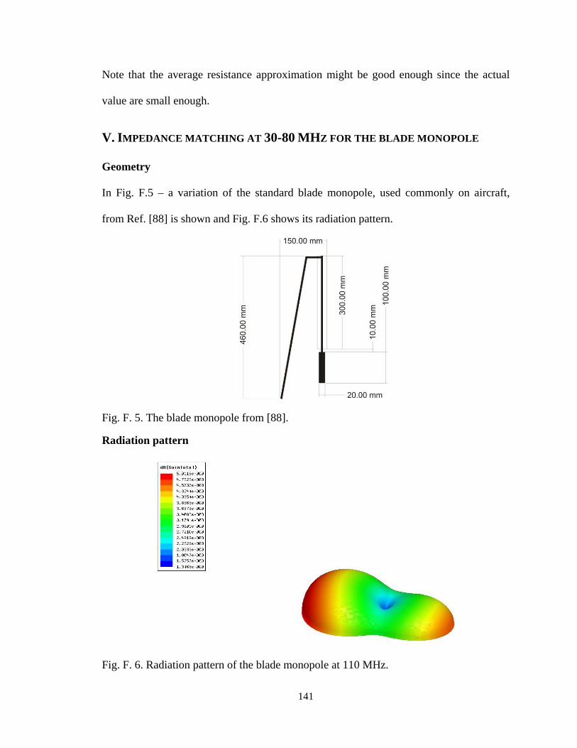
141
Note that the average resistance approximation might be good enough since the actual
value are small enough.
V. IMPEDANCE MATCHING AT 30-80 MHZ FOR THE BLADE MONOPOLE
Geometry
In Fig. F.5 – a variation of the standard blade monopole, used commonly on aircraft,
from Ref. [88] is shown and Fig. F.6 shows its radiation pattern.
Fig. F. 5. The blade monopole from [88].
Radiation pattern
Fig. F. 6. Radiation pattern of the blade monopole at 110 MHz.

142
Matching network
A 4-component impedance-matching network [86], [87] shown in Fig. F.7, is used for the
blade monopole geometry shown in Fig. F.5. The network is composed of a series
inductor, a tank circuit in shunt, and a resistor. This network provides a consistent VSWR
over the band. At the same time, the matching network is lossy: it includes a tank circuit
in series with a resistor. The required resistor value is approximately equal to AR .
Fig. F. 7. Antenna matching: the impedance-matching network and a step-up transformer.
An equivalent circuit for such an antenna is the series LCR circuit. The DR antenna as
well as the blade monopole introduced above in Fig. F. 4 belongs to exactly this type.
The matching network outputs a real, but still small impedance on the order of AR
uniformly over the band. Therefore, it should be followed by a step-up impedance
transformer as shown in Fig. F.7. An alternative may be to switch the matching network
and the low-loss transformer in the RX mode at least, which might, under certain
conditions, result in a better overall power efficiency.

143
We calculate the transducer gain for this network as follows
22
)()(
)()(4)(
ωω
ωωω
TA
T
ZZ
RRT
+=
Here, we calculate the Thevenin equivalent for the network as shown in Fig. F.8. The
antenna resistance R = RA from Fig. F. 7.
Fig. F.8. Transformation of the matching network: a) lossy matching network representation, b) Thévenin-equivalent circuit representation. The matching network does not include transformers.
Since the network in Fig. F. 7 is lossy, the one to one relationship between the transducer
gain and the reflection coefficient doesn't exist. Therefore we calculate the reflection
coefficient and hence, VSWR at the input to the network cascaded with the antenna's
impedance.
The result of model parameter extraction for the blade monopole yielded the results
shown in Fig. F. 9. Here we see that an acceptable agreement is present for the reactance

144
data while the resistance has been approximated to be constant over the band. This
resistance value is indeed quite low and hence we determined a matching impedance of
1Ω to match for prior to the transformer. We note the presence of a resonance within the
band at approximately 47 MHz. This resonance essentially validates the LCR model for
the antenna as well.
Fig. F. 9. Comparison of the impedance data from simulation and the extracted LCR model for the blade monopole.
Results
By using the appropriate matching network, we calculate the VSWR and the transducer
gain as a function of frequency. The band to be matched over is 30 - 80 MHz. The use of
the reflection-less equalizer gives a flat VSWR profile, while the transcuer gain behavior
over the band shows the narrowband response.

145
Fig. F. 10. VSWR at the input to the reflection less equalizer and transducer gain for the blade monopole antenna.

146
Appendix G – Code function [ZA] = dipole(f, dipole_x, dipole_y);
% Dipole self-impedance: analytical solution for the cylindrical or strip dipole
% C.-T. Tai and S. A. Long, “Dipoles and monopoles,” in: Antenna Engineering Handbook,
% John L. Volakis, Ed., Mc Graw Hill, 2007, fourth edition, pp. 4-3 to
% 4-32.
% EM data
const.epsilon = 8.85418782e-012; % ANSOFT HFSS value
const.mu = 1.25663706e-006; % ANSOFT HFSS value
const.c = 1/sqrt(const.epsilon*const.mu);
const.eta = sqrt(const.mu/const.epsilon);
k = 2*pi*f/const.c;
kl = k*dipole_y/2;
a = dipole_x/2; % equivalent radius
l = dipole_y/2;
R = -0.4787 + 7.3246*kl + 0.3963*kl.^2 + 15.6131*kl.^3;
R(find(R < 0)) = 0;
X = -0.4456 + 17.00826*kl - 8.6793*kl.^2 + 9.6031*kl.^3;
ZA = R - j*(120*(log(l/a)-1)*cot(kl)-X); % Antenna impedance

147
function [ZA,L] = smallLoop(f,loop_a,loop_b)
% This function calculates the Impedance of a small circular loop based
on input parameters which are the frequency, loop radius and loop
conductor width.
% EM data
const.epsilon = 8.85418782e-012; % ANSOFT HFSS value
const.mu = 1.25663706e-006; % ANSOFT HFSS value
const.c = 1/sqrt(const.epsilon*const.mu);
const.eta = sqrt(const.mu/const.epsilon);
lambda = const.c./f;
Circ_umf = 2*pi*loop_a; % loop circumference
Rr = 20*(pi^2)*((Circ_umf./lambda).^4); % Radiation resistance
of a small circular loop
L = const.mu*loop_a*(log(8*loop_a/loop_b) - 2); % Inductance
of small circular loop
Xl = 2*pi.*f*L;
ZA = Rr + 1i.*Xl;

148
% A script for matching circuit estimation at different center frequencies fc and bandwidths B. Saves the matching circuit parameters and optimized performance dataset for every parameter set.
% S. Makarov and V. Iyer, ECE Dept., WPI Aug. 2008
dipole_y = 230e-3; % dipole length (m)
Rg = 50; % generator resistance
f_res = 3e8/(2*dipole_y); % resonant frequency (ideal; half-wave resonance)
Ls = [1 1 1 1 1]*eps; % lower initial bounds for the parameter search
Us = [2e-6 1e-6 100e-12 1e-6 100e-12]; % upper initial bounds for the parameter search
% (optimized for 150mm length)
Us = Us*(dipole_y/150e-3); % good for any length
dipole_lt = [20]; % length to width ratio
DCF = [0.5]; % relative center frequency vs. f_res
FB = [0.5]; % fractional bandwidth
MeanGain = zeros( length(dipole_lt), length(DCF), length(FB));
VarGain = zeros( length(dipole_lt), length(DCF), length(FB));
CP_nHpF = zeros(5, length(dipole_lt), length(DCF), length(FB));
for ilt = 1:length(dipole_lt)
for iDCF = 1:length(DCF)
for iFB = 1:length(FB)
dcf = DCF(iDCF); fb = FB(iFB);
run.center_freq = dcf;
run.bandwidth = fb;
run.dipole_lt = dipole_lt(ilt);
%---------------------------------------------------------------
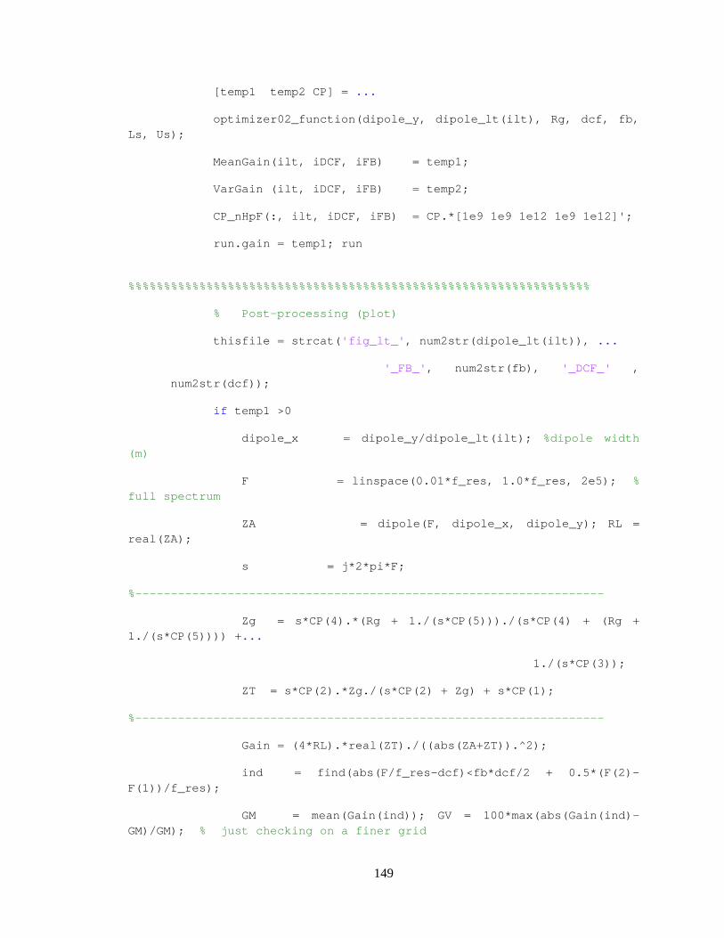
149
[temp1 temp2 CP] = ...
optimizer02_function(dipole_y, dipole_lt(ilt), Rg, dcf, fb, Ls, Us);
MeanGain(ilt, iDCF, iFB) = temp1;
VarGain (ilt, iDCF, iFB) = temp2;
CP_nHpF(:, ilt, iDCF, iFB) = CP.*[1e9 1e9 1e12 1e9 1e12]';
run.gain = temp1; run
%%%%%%%%%%%%%%%%%%%%%%%%%%%%%%%%%%%%%%%%%%%%%%%%%%%%%%%%%%%%%%%%%
% Post-processing (plot)
thisfile = strcat('fig_lt_', num2str(dipole_lt(ilt)), ...
'_FB_', num2str(fb), '_DCF_' , num2str(dcf));
if temp1 >0
dipole_x = dipole_y/dipole_lt(ilt); %dipole width (m)
F = linspace(0.01*f_res, 1.0*f_res, 2e5); % full spectrum
ZA = dipole(F, dipole_x, dipole_y); RL = real(ZA);
s = j*2*pi*F;
%------------------------------------------------------------------
Zg = s*CP(4).*(Rg + 1./(s*CP(5)))./(s*CP(4) + (Rg + 1./(s*CP(5)))) +...
1./(s*CP(3));
ZT = s*CP(2).*Zg./(s*CP(2) + Zg) + s*CP(1);
%------------------------------------------------------------------
Gain = (4*RL).*real(ZT)./((abs(ZA+ZT)).^2);
ind = find(abs(F/f_res-dcf)<fb*dcf/2 + 0.5*(F(2)-F(1))/f_res);
GM = mean(Gain(ind)); GV = 100*max(abs(Gain(ind)-GM)/GM); % just checking on a finer grid

150
h = figure; semilogy(F/f_res, Gain, 'LineWidth', 2); grid on; hold on;
line([dcf-fb*dcf/2 dcf-fb*dcf/2], [1e-4 1], 'Color', 'g');
line([dcf+fb*dcf/2 dcf+fb*dcf/2], [1e-4 1], 'Color', 'g');
line([dcf, dcf], [1e-4 1], 'LineWidth', 2, 'Color', 'r');
title(strcat('Average gain, a.u. = ', num2str(GM), '; Variation(%) =', num2str(GV)));
xlabel('f/f_res'); ylabel('Gain, a.u.'); axis([min(F/f_res) max(F/f_res) 1e-4, 1]);
saveas(h, strcat(thisfile, '.fig'));
end
%%%%%%%%%%%%%%%%%%%%%%%%%%%%%%%%%%%%%%%%%%%%%%%%%%%%%%%%%%%%%%%%%
close all;
end
end
end
save;

151
function [MeanGain VarGain CP] = optimizer02_function(dipole_y, dipole_lt, Rg, DCF, FB, Ls, Us);
% Matching circuit optimizer for a dipole - a reflective equalizer
% Direct search on 1D arrays; the search here is limited to 5 circuit
% elements
%
% dipole_y - dipole length
% dipole_lt - length-to-width or length-to-radius ratio
% DCF - relative center frequency fc/f_res
% FB - fractional bandwidth vs. center frequency
% Ls - lower bound of search parameters
% Us - upper bound of search parameters
% There are no output arguments; the function saves all data in a mat
% file.
%
% 1D Array assembly in parameter space:
% (M(1) = 3; M(2) = 2; M(3) = 2; M(4) = 2; M(5) = 1)
% [1 2 3][1 2 3][1 2 3][1 2 3][1 2 3][1 2 3][1 2 3][1 2 3] M(1) A(1, :)
% [1 1 1][2 2 2][1 1 1][2 2 2][1 1 1][2 2 2][1 1 1][2 2 2] M(2) A(2, :)
% [1 1 1][1 1 1][2 2 2][2 2 2][1 1 1][1 1 1][2 2 2][2 2 2] M(3) A(3, :)
% [1 1 1][1 1 1][1 1 1][1 1 1][2 2 2][2 2 2][2 2 2][2 2 2] M(4) A(4, :)
% [1 1 1][1 1 1][1 1 1][1 1 1][1 1 1][1 1 1][1 1 1][1 1 1] M(5) A(5, :)
% S. Makarov and V. Iyer, ECE Dept., WPI Aug. 2008

152
% Antenna/generator/bandwidth
dipole_x = dipole_y/dipole_lt; % dipole width (m)
f_res = 3e8/(2*dipole_y); % resonant frequency (ideal; half-wave resonance)
B = 4; % number of frequency observation points over the bandwidth
f_center = DCF*f_res; % absolute center frequency vs. f_res
bandwidth = FB*f_center; % absolute bandwidth
% Bandwidth discretization for initial and final search
f = linspace(f_center-bandwidth/2, f_center+bandwidth/2, B); % initial search
s = j*2*pi*f; % initial search
ZA = dipole(f, dipole_x, dipole_y); RL = real(ZA); % initial search
f1 = linspace(f_center-bandwidth/2, f_center+bandwidth/2, 16*B); % final search
s1 = j*2*pi*f1; % final search
ZA1 = dipole(f1, dipole_x, dipole_y); RL1 = real(ZA1); % final search
% Equalizer circuit
M(1) = 128; % first parameter search space
M(2) = 064; % second parameter search space
M(3) = 032; % third parameter search space
M(4) = 016; % fourth parameter search space
M(5) = 016; % fifth parameter search space
A = complex(zeros(5, prod(M))); % all parameter values assembled in linear arrays
153
Gain = zeros(1, prod(M)); % the generator gain
Par_min = Ls; % lower initial bounds for the parameter search
Par_max = Us; % upper initial bounds for the parameter search
% main loop over the seach domains (the domain is refined at every step)
VarGain = 0; % controls gain variation over the band (global)
MeanGain = 0; % controls mean gain over the band (global)
TGain = 0; % controls max mean gain over the band (loop)
TGain_plot = TGain; % visualize gain improvement over the seach
CP = zeros(length(M), 1); % circuit parameters to be found (global)
search_domains = 7; % number of domain iterations
for search_domains_ind = 1:search_domains
StopGain = 0; tic % controls the current iteration
% Circuit parameters (cell arrays)
par(1) = linspace(Par_min(1), Par_max(1), M(1)); % L1 here (0)
par(2) = linspace(Par_min(2), Par_max(2), M(2)); % L2 here (inf)
par(3) = linspace(Par_min(3), Par_max(3), M(3)); % C3 here (inf)
par(4) = linspace(Par_min(4), Par_max(4), M(4)); % L4 here (inf)
par(5) = linspace(Par_min(5), Par_max(5), M(5)); % C5 here (inf)
% Fill out the 1D arrays
temp = 1;

154
for m = 1:length(M)
if m >1
temp = prod(M(1:m-1));
end
block_length = temp;
no_of_blocks = prod(M(m+1:end));
A(m, :) = reshape(repmat(parm, block_length, no_of_blocks), 1, prod(M));
end
% Find min power over the entire frequency band for every particular parameter set
for m = 1:length(s)
%------------------------------------------------------------------
Zg = s(m)*A(4, :).*(Rg + 1./(s(m)*A(5, :)))./( s(m)*A(4, :) + (Rg+1./(s(m)*A(5, :))) ) +...
1./(s(m)*A(3, :));
ZT = s(m)*A(2, :).*Zg./(s(m)*A(2, :) + Zg) + s(m)*A(1, :);
%------------------------------------------------------------------
if m ==1
Gain =(4*RL(m))*real(ZT)./((abs(ZA(m)+ZT)).^2);
else
Gain = min(Gain,(4*RL(m))*real(ZT)./((abs(ZA(m)+ZT)).^2));
end
end
% Sort that power (most CPU time-involved step)
[dummy index] = sort(uint16(1e6*Gain), 'descend');
% Check if the +/-25% criterion of gain variation is really satisfied on a finer grid
155
for p = 1:round(prod(M)/128) % a critical point: only initial values are examined
temp = index(p); % index into arrays
a = A(:, temp); % obtain particular circuit parameters
%--------------------------------------------------
Zg_ = s1*a(4).*(Rg + 1./(s1*a(5)))./( s1*a(4) + (Rg+1./(s1*a(5))) ) +...
1./(s1*a(3));
ZT_ = s1*a(2).*Zg_./(s1*a(2) + Zg_) + s1*a(1);
%--------------------------------------------------
Gain_ = (4*RL1).*real(ZT_)./((abs(ZA1+ZT_)).^2);
MGain = mean(Gain_); % local mean gain
VGain = 100*max(abs(Gain_-MGain)/MGain); % local gain variation
if (VGain <= 25) % +/-25% satisfied
if (MGain> TGain) % search for a higher average gain
VarGain = VGain; MeanGain = MGain; CP = a;
TGain = MGain; % TGain controls the loop
StopGain = MGain; % StopGain controls the loop iteration
TGain_plot = [TGain_plot TGain]; % Convergence history
plot(TGain_plot, '-bs',...; % Plot converegence history
'MarkerEdgeColor', 'k', 'MarkerFaceColor', 'g', 'MarkerSize',10);
title('Gain convergence'); hold on; grid on; drawnow;
end
156
end
end
if TGain == 0 return; end; % found none - exit this function
if StopGain == 0 break; end; % found none for this iteration (no more iterations)
% Find the bettter search range based on the found circuit parameters (+/- 50%)
Par_min = 0.50*CP;
Par_max = 1.50*CP; toc
End
157
% Bode-Fano criterion for the dipole
% Dipole parameters
dipole_y = 230e-3; % dipole length (m)
dipole_lt = 10;
dipole_x = dipole_y/dipole_lt; % dipole width (m)
f_res = 3e8/(2*dipole_y)
f_center = [0.05:0.01:0.5]*f_res;
b = figure;
z = pi/2*f_center/f_res;
a = dipole_x/2; % equivalent radius
l = dipole_y/2; % half-length
R = -0.4787 + 7.3246*z + 0.3963*z.^2 + 15.6131*z.^3;
R = R./2; % Monopole impedance is half of dipole
GBP = 4*pi^2*R./480.*(f_center/f_res)/(log(l/a)-1);
B = 0.50;
G = 1- exp(-GBP*(1-(B^2)/4)/B);
semilogy(f_center/f_res, G, 'r', 'LineWidth', 2);
grid on;
hold on
axis([min(f_center/f_res), max(f_center/f_res), 1e-3, 1])
158
% This script calculates the upper bound on system efficiency for
antennas (below first resonance) and matching network combination. The
antenna is assumed to be lossless and its Q is approximated using
Q(w=w_0) = X(w=w_0)/R_r(w=w_0). This upper bound holds under the
following conditions
%
% 1. All elements in network of the same type electric/magnetic have
equal Q
% 2. These elements store energy in a form opposite to the antenna
% 3. Generator is lossless
% Author: V. Iyer, S. Makarov, WPI, Oct.2008
%
%% SMALL DIPOLE CALCULATION
dipole_y = 150e-3; % dipole length (m)
Rg = 50; % generator resistance
f_res = 3e8/(2*dipole_y); % resonant frequency (ideal;
half-wave resonance)
dipole_lt = [5 10 50]; % length to width ratio
DCF = [0.05:0.05:0.5]; % relative center
frequency vs. f_res
f_center = DCF*f_res; % absolute center frequency
vs. f_res
f = linspace(f_center(1), f_center(end), 64);
figure
Antenna_Q = zeros(3,length(f));
for loop = 1:length(dipole_lt)
dipole_x = dipole_y/dipole_lt(loop);
ZA = dipole(f, dipole_x, dipole_y);
R = real(ZA);
X = imag(ZA);
% Q approximation for antenna
Q_a = abs(X)./R;
eta_a = 1;

159
% component Q - Matching Network comprising of L section L1, L2 -
% CHANGE TO 55
Q_mn = 55;
eta_mn = 1./(1 + (Q_a./Q_mn));
% System Efficiency
eta_s = eta_a*eta_mn*100;
Antenna_Q(loop,:) = Q_a;
semilogy(f/f_res, eta_s,'LineWidth',2)
grid on
xlabel('f_c/f_r_e_s')
ylabel('% System Efficiency - \eta_s')
title('Efficiency bound at center of band for short dipole - 3
geometries')
hold all
end
legend('l_A/d = 5','l_A/d = 10','l_A/d = 50')
axis([min(f/f_res) max(f/f_res) 1e-2 1e2])
figure
for loop = 1:length(dipole_lt)
plot(f/f_res,Antenna_Q(loop,:));
hold all
end
grid on
xlabel('f_c/f_r_e_s')
ylabel('Q_A_N_T')
title('Antenna Q factor - Dipole')
legend('l_A/d = 5','l_A/d = 10','l_A/d = 50')
%% SMALL CIRCULAR LOOP CALCULATION
f_res = 1e9;
loop_a = 3e8/(2*pi*f_res); % loop radius
Circ_umf = 2*pi*loop_a; % loop circumference
Rg = 50; % generator resistance
Omega = [8 10 12]; % Conductor thickness factor
f_min = 3e8/(10*Circ_umf);
f_max = 3e8/(4*Circ_umf);

160
f_min = f_min/f_res;f_max = f_max/f_res;
DCF = f_min:f_min/2:f_max; % relative center
frequency vs. f_res
f_center = DCF*f_res; % absolute center frequency
vs. f_res
% Set of Center Frequencies
f = linspace(f_center(1), f_center(end), 64); % final
search
figure
Antenna_Q = zeros(3,length(f));
for loop = 1:length(Omega)
loop_b = Circ_umf*exp(-Omega(loop)/2); % loop conductor
width (m)
ZA = smallLoop(f, loop_a, loop_b);
R = real(ZA); % final search
X = imag(ZA);
% Q approximation for antenna
Q_a = abs(X)./R;
eta_a = 1;
% component Q - Matching Network comprising of C section C1, C2
Q_mn = 1000;
eta_mn = 1./(1 + (Q_a./Q_mn));
% System Efficiency
eta_s = eta_a*eta_mn*100;
% Plots
semilogy(f/f_res, eta_s,'LineWidth',2)
grid on
xlabel('f_c/f_r_e_s')
ylabel('% System Efficiency - \eta_s')
title('Efficiency bound at center of band for small Loop - 3
geometries')
hold all
Antenna_Q(loop,:) = Q_a;
end
legend('\Omega = 8','\Omega = 10','\Omega = 12')
axis([min(f/f_res) max(f/f_res) 1 1e2])
161
figure
for loop = 1:length(dipole_lt)
plot(f/f_res,Antenna_Q(loop,:));
hold all
end
grid on
xlabel('f_c/f_r_e_s')
ylabel('Q_A_N_T')
title('Antenna Q factor - Loop')
legend('\Omega = 8','\Omega = 10','\Omega = 12')

162
% Matching Circuit design for a dipole - Reflective Equalizer % HYBRID GA % Using Genetic Algorithm - Vectorized % Using Pattern Search to refine % Both Low pass and High pass + L - section are available for design % The population size has been reduced and a no. of independent GA runs
are used to determine the best candidate % STATUS : Currently, it uses pattern search on the best starting % point candidate after a certain number of GA runs have occurred. % % Authors : - Vishwanath Iyer, Sergey Makarov, ECE Dept.,WPI,Aug. 2008 %
%% Antenna/generator/bandwidth DCF = 5/12; % relative center frequency
vs. f_res FB = 0.4; % fractional bandwidth dipole_y = 500e-3; % dipole length (m) dipole_lt = 0.5/0.001; % length to width ratio dipole_x = dipole_y/dipole_lt; % dipole width (m) f_res = 3e8/(2*dipole_y); % resonant frequency (ideal;
half-wave resonance) Rg = 50; % generator resistance B = 32; % number of frequency
observation points over the bandwidth f_center = DCF*f_res; % absolute center frequency
vs. f_res bandwidth = FB*f_center; % absolute bandwidth
% Bandwidth discretization for initial and final search f = linspace(f_center-bandwidth/2, f_center+bandwidth/2, B); %
initial search s = j*2*pi*f; %
initial search ZA = dipole(f, dipole_x, dipole_y); RL = real(ZA); %
initial search
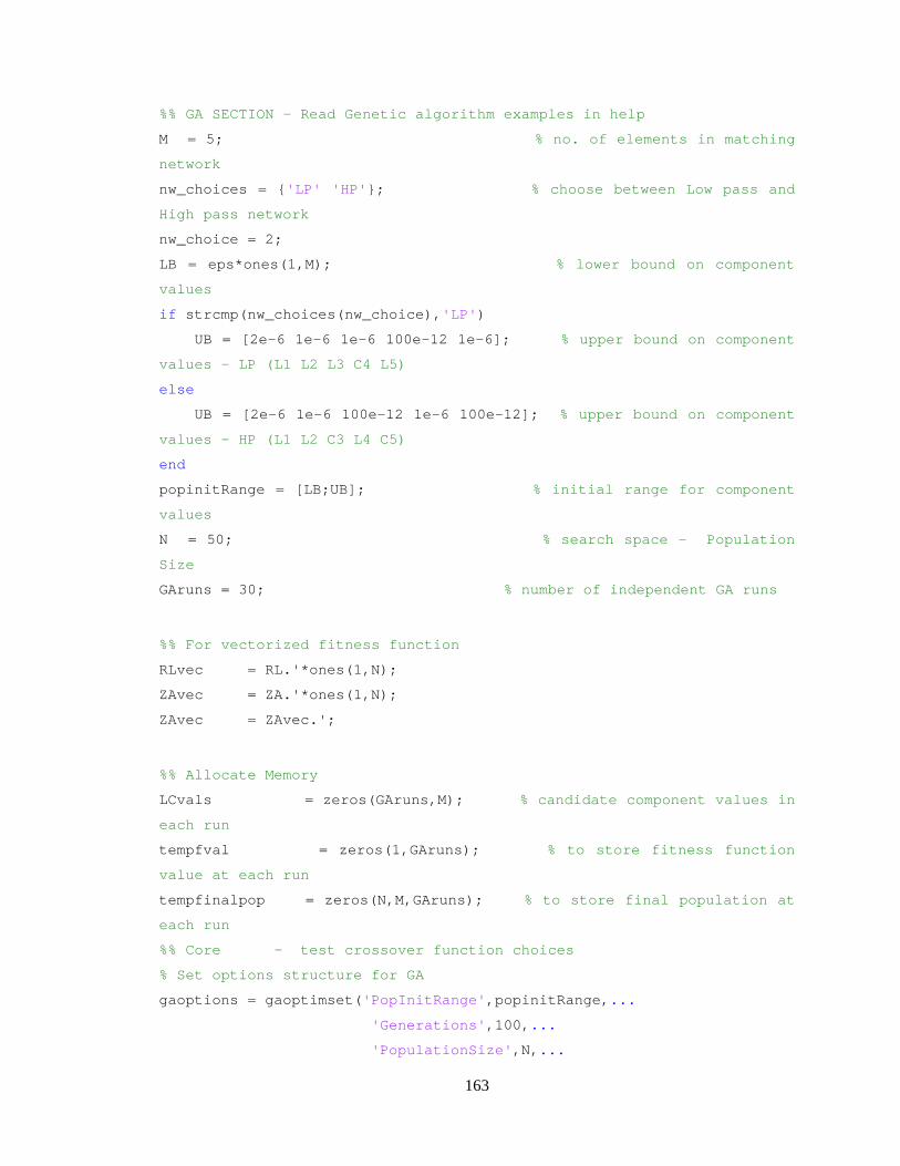
163
%% GA SECTION - Read Genetic algorithm examples in help M = 5; % no. of elements in matching
network nw_choices = 'LP' 'HP'; % choose between Low pass and
High pass network nw_choice = 2; LB = eps*ones(1,M); % lower bound on component
values if strcmp(nw_choices(nw_choice),'LP') UB = [2e-6 1e-6 1e-6 100e-12 1e-6]; % upper bound on component
values - LP (L1 L2 L3 C4 L5) else UB = [2e-6 1e-6 100e-12 1e-6 100e-12]; % upper bound on component
values - HP (L1 L2 C3 L4 C5) end popinitRange = [LB;UB]; % initial range for component
values N = 50; % search space - Population
Size GAruns = 30; % number of independent GA runs
%% For vectorized fitness function RLvec = RL.'*ones(1,N); ZAvec = ZA.'*ones(1,N); ZAvec = ZAvec.';
%% Allocate Memory LCvals = zeros(GAruns,M); % candidate component values in
each run tempfval = zeros(1,GAruns); % to store fitness function
value at each run tempfinalpop = zeros(N,M,GAruns); % to store final population at
each run %% Core - test crossover function choices % Set options structure for GA gaoptions = gaoptimset('PopInitRange',popinitRange,... 'Generations',100,... 'PopulationSize',N,...

164
'EliteCount',round(N/2),... 'MutationFcn',@mutationadaptfeasible,... 'MigrationDirection','forward',... 'MigrationInterval',2,... 'MigrationFraction',0.35,... 'SelectionFcn',@selectionremainder,... 'PenaltyFactor',20000,... 'TolFun',1e-9,... 'StallTimeLimit',inf,... 'StallGenLimit',inf,... 'Display','iter',... 'Vectorized','on',... 'PlotFcns', @gaplotbestf);
% Set options structure for Pattern Search afterN_GA_runs = 5; % No. of GA runs after
which to refine result PSoptions = psoptimset('CompletePoll','on',... 'CompleteSearch','on',... 'SearchMethod',@MADSPositiveBasisNp1,... 'InitialMeshSize',1e-14,... 'MaxIter',30*M,... 'TolMesh',1e-16,... 'TolCon',1e-16,... 'TolX',1e-16,... 'TolFun',1e-16,... 'PenaltyFactor',100,... 'Cache','on',... 'PlotFcns',@psplotbestf,... 'Vectorized','off');
FitnessFunction = @(tempLCvals)
GAfitnessFunc_Vec(tempLCvals,s,Rg,ZAvec,RLvec,nw_choice); numberOfVariables = M; indx_prev = 0; tic for loop2 = 1:GAruns
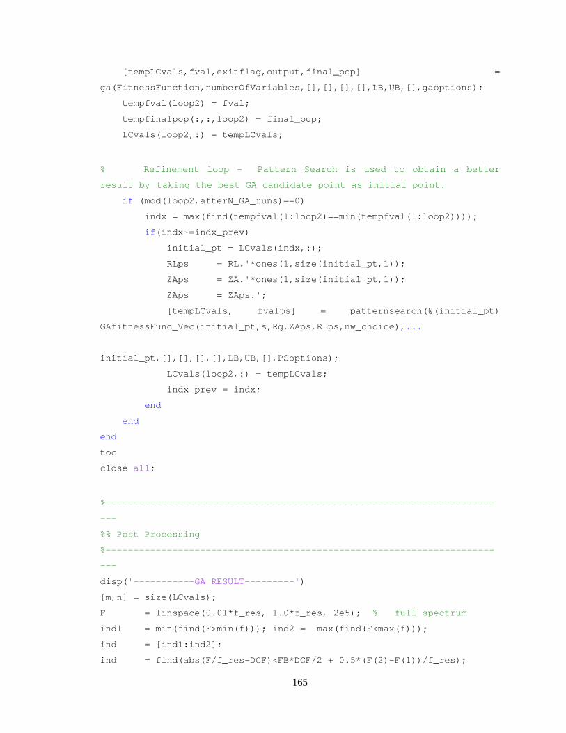
165
[tempLCvals,fval,exitflag,output,final_pop] =
ga(FitnessFunction,numberOfVariables,[],[],[],[],LB,UB,[],gaoptions); tempfval(loop2) = fval; tempfinalpop(:,:,loop2) = final_pop; LCvals(loop2,:) = tempLCvals;
% Refinement loop - Pattern Search is used to obtain a better
result by taking the best GA candidate point as initial point. if (mod(loop2,afterN_GA_runs)==0) indx = max(find(tempfval(1:loop2)==min(tempfval(1:loop2)))); if(indx~=indx_prev) initial_pt = LCvals(indx,:); RLps = RL.'*ones(1,size(initial_pt,1)); ZAps = ZA.'*ones(1,size(initial_pt,1)); ZAps = ZAps.'; [tempLCvals, fvalps] = patternsearch(@(initial_pt)
GAfitnessFunc_Vec(initial_pt,s,Rg,ZAps,RLps,nw_choice),...
initial_pt,[],[],[],[],LB,UB,[],PSoptions); LCvals(loop2,:) = tempLCvals; indx_prev = indx; end end end toc close all;
%----------------------------------------------------------------------
--- %% Post Processing %----------------------------------------------------------------------
--- disp('-----------GA RESULT---------') [m,n] = size(LCvals); F = linspace(0.01*f_res, 1.0*f_res, 2e5); % full spectrum ind1 = min(find(F>min(f))); ind2 = max(find(F<max(f))); ind = [ind1:ind2]; ind = find(abs(F/f_res-DCF)<FB*DCF/2 + 0.5*(F(2)-F(1))/f_res);
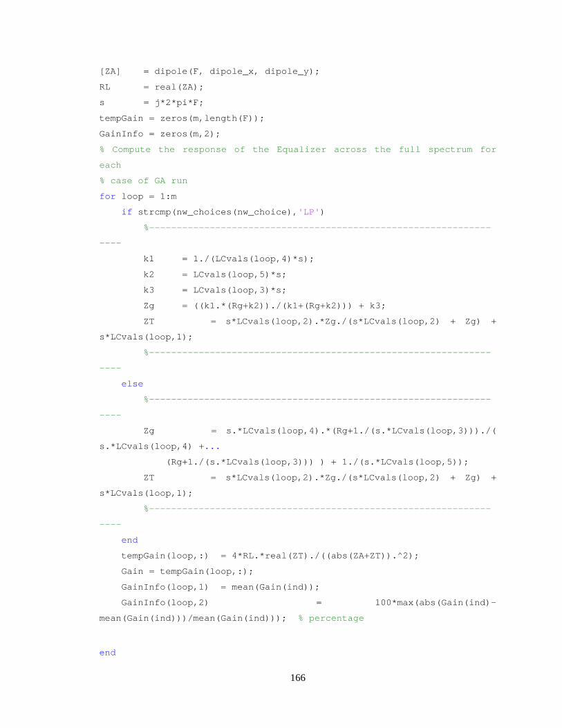
166
[ZA] = dipole(F, dipole_x, dipole_y); RL = real(ZA); s = j*2*pi*F; tempGain = zeros(m,length(F)); GainInfo = zeros(m,2); % Compute the response of the Equalizer across the full spectrum for
each % case of GA run for loop = 1:m if strcmp(nw_choices(nw_choice),'LP') %--------------------------------------------------------------
---- k1 = 1./(LCvals(loop,4)*s); k2 = LCvals(loop,5)*s; k3 = LCvals(loop,3)*s; Zg = ((k1.*(Rg+k2))./(k1+(Rg+k2))) + k3; ZT = s*LCvals(loop,2).*Zg./(s*LCvals(loop,2) + Zg) +
s*LCvals(loop,1); %--------------------------------------------------------------
---- else %--------------------------------------------------------------
---- Zg = s.*LCvals(loop,4).*(Rg+1./(s.*LCvals(loop,3)))./(
s.*LCvals(loop,4) +... (Rg+1./(s.*LCvals(loop,3))) ) + 1./(s.*LCvals(loop,5)); ZT = s*LCvals(loop,2).*Zg./(s*LCvals(loop,2) + Zg) +
s*LCvals(loop,1); %--------------------------------------------------------------
---- end tempGain(loop,:) = 4*RL.*real(ZT)./((abs(ZA+ZT)).^2); Gain = tempGain(loop,:); GainInfo(loop,1) = mean(Gain(ind)); GainInfo(loop,2) = 100*max(abs(Gain(ind)-
mean(Gain(ind)))/mean(Gain(ind))); % percentage
end

167
% Find which cases satisfy Gain Variation criterion best_cases = find(GainInfo(:,2)<25); GainData = GainInfo(best_cases,:); Gainbest = tempGain(best_cases,:); LCval_best = LCvals(best_cases,:);
% Plot 2 cases and save important parameters to file if (GainData(:))
%-------- Find the best case for least average gain variation ---------
---------- ind = find(GainData(:,2)==min(GainData(:,2))); Gain1 = GainData(ind,1) leastGainVar = GainData(ind,2)
% ------- Find the highest acheived average gain (less than 25% still
valid) -------------------------------- ind2 = find(GainData(:,1)==max(GainData(:,1))); highestGain = GainData(ind2,1) GainVar2 = GainData(ind2,2)
% -------Plot both cases ----------------------------------------------
-- figure plot(F/f_res, 10*log10(Gainbest(ind,:)),'LineWidth', 2); grid on; title(strcat('Average Gain, a.u. for ',' ',nw_choices(nw_choice),'
n/w -(Least variation) = ' ,num2str(Gain1) ,' ;Gain variation (%) =
',num2str(leastGainVar))); line([DCF-FB*DCF/2 DCF-FB*DCF/2], [-30 0], 'Color', 'g'); line([DCF+FB*DCF/2 DCF+FB*DCF/2], [-30 0], 'Color', 'g'); line([DCF, DCF], [-30 0], 'LineWidth', 2, 'Color',
'r'); xlabel('f/f_res'); ylabel('Gain, dB'); axis([min(F/f_res) max(F/f_res) -30, 0]);

168
figure plot(F/f_res, 10*log10(Gainbest(ind2,:)),'LineWidth', 2); grid on; title(strcat('Average gain, a.u. for ',' ',nw_choices(nw_choice),'
n/w -(Highest avg. gain) = ',num2str(highestGain), ' ;Gain variation(%)
= ', num2str(GainVar2))); line([DCF-FB*DCF/2 DCF-FB*DCF/2], [-30 0], 'Color', 'g'); line([DCF+FB*DCF/2 DCF+FB*DCF/2], [-30 0], 'Color', 'g'); line([DCF, DCF], [-30 0], 'LineWidth', 2, 'Color',
'r'); xlabel('f/f_res'); ylabel('Gain, dB'); axis([min(F/f_res) max(F/f_res) -30, 0]);
% -----------------------Display circuit parameters and Save File -----
---------------------------------- if strcmp(nw_choices(nw_choice),'LP')
% Component values circuit.L1 = LCval_best(ind,1)*1e6; circuit.L2 = LCval_best(ind,2)*1e6; circuit.L3 = LCval_best(ind,3)*1e6; circuit.C4 = LCval_best(ind,4)*1e12; circuit.L5 = LCval_best(ind,5)*1e6; disp(strcat('------Component values for LP n/w with least avg gain
variation')) circuit
% Component values circuit2.L1 = LCval_best(ind2,1)*1e6; circuit2.L2 = LCval_best(ind2,2)*1e6; circuit2.L3 = LCval_best(ind2,3)*1e6; circuit2.C4 = LCval_best(ind2,4)*1e12; circuit2.L5 = LCval_best(ind2,5)*1e6; disp(strcat('------Component values for LP n/w with highest avg
gain')) circuit2 filename = strcat('GA_circuit5LP_DCF=',num2str(DCF));

169
filename = strcat(filename,'_FB='); filename = strcat(filename,num2str(FB)); filename = strcat(filename,'.mat'); save(filename, 'DCF', 'FB', 'GainData', 'Gainbest', 'LCval_best',
'F','gaoptions','PSoptions'); else % Component values circuit.L1 = LCval_best(ind,1)*1e6; circuit.L2 = LCval_best(ind,2)*1e6; circuit.C3 = LCval_best(ind,3)*1e12; circuit.L4 = LCval_best(ind,4)*1e6; circuit.C5 = LCval_best(ind,5)*1e12; disp(strcat('------Component values for HP n/w with least avg gain
variation')) circuit % Component values circuit2.L1 = LCval_best(ind2,1)*1e6; circuit2.L2 = LCval_best(ind2,2)*1e6; circuit2.C3 = LCval_best(ind2,3)*1e12; circuit2.L4 = LCval_best(ind2,4)*1e6; circuit2.C5 = LCval_best(ind2,5)*1e12; disp('------Component values for HP n/w with highest avg gain') circuit2
filename = strcat('GA_circuit5HP_DCF=',num2str(DCF)); filename = strcat(filename,'_FB='); filename = strcat(filename,num2str(FB)); filename = strcat(filename,'.mat'); save(filename, 'DCF', 'FB', 'GainData', 'Gainbest', 'LCval_best',
'F','gaoptions','PSoptions'); end else disp('---------No Matching network found------') end

170
function output = GAfitnessFunc_Vec(LCvals,s,Rg,ZA,RL,nw_choice) % Handles both Low pass and high pass cascades to the L- section. % Vectorized fitness function; % LCvals - is of the population size, s is a vector % ZA and RL have to be supplied as matrices of size NX popsize where N
% is no. of freq points when used by GA
if (nw_choice==1) % Impedance calculation for Low pass T network k1 = 1./(LCvals(:,4)*s); k3 = LCvals(:,3)*s; k2 = LCvals(:,5)*s;
Zg = ((k1.*(Rg+k2))./(k1+(Rg+k2))) + k3;
ZT = (LCvals(:,2)*s).*Zg./((LCvals(:,2)*s) + Zg) +
(LCvals(:,1)*s);
else % Impedance calculation for high pass T network k1 = (LCvals(:,4)*s); k2 = (Rg + 1./(LCvals(:,3)*s)); k3 = 1./(LCvals(:,5)*s);
Zg = ((k1.*k2)./(k1+k2)) + k3;
ZT = (LCvals(:,2)*s).*Zg./((LCvals(:,2)*s) + Zg) +
(LCvals(:,1)*s); end
% Gain calculations tempZ = real(ZT)./((abs(ZA+ZT)).^2); Gain = 4*RL.*tempZ.';
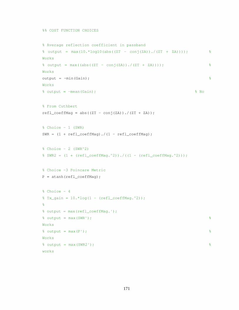
171
%% COST FUNCTION CHOICES
% Average reflection coefficient in passband % output = max(10.*log10(abs((ZT - conj(ZA))./(ZT + ZA)))); %
Works % output = max((abs((ZT - conj(ZA))./(ZT + ZA)))); %
Works output = -min(Gain); %
Works % output = -mean(Gain); % No
% From Cuthbert refl_coeffMag = abs((ZT - conj(ZA))./(ZT + ZA));
% Choice - 1 (SWR) SWR = (1 + refl_coeffMag)./(1 - refl_coeffMag);
% Choice - 2 (SWR^2) % SWR2 = (1 + (refl_coeffMag.^2))./((1 - (refl_coeffMag.^2)));
% Choice -3 Poincare Metric P = atanh(refl_coeffMag);
% Choice - 4 % Tx_gain = 10.*log(1 - (refl_coeffMag.^2)); % % output = max(refl_coeffMag.'); % output = max(SWR'); %
Works % output = max(P'); %
Works % output = max(SWR2'); %
works

172
% This script attempts to calculate the R,L and C values of a antenna model directly from the simulated impedance data
% Author: Vishwanath Iyer, Antenna Lab, WPI, 2008
%%
% Load csv data from file
strip4Z = csvread('Z:\Vishwanath\DRA_materials\DR_deepSearch\Brian_DR\strip4.csv');
%%%%%%%%%%%%%%%%%%%%%%%%%% Strip 4 %%%%%%%%%%%%%%%%%%%%%%%%%%%%%%%%%%%%%%%%%%%%%
freq = strip4Z(:,1);
Z_A4 = strip4Z(:,2) + 1i.*strip4Z(:,3);
% Set up matching band and extract data
f_min = 28; % MHz
f_max = 78; % MHz
f_c = (f_min + f_max)/2;
indx_min = find(freq>=f_min);indx_min = indx_min(1);
indx_max = find(freq>=f_max);indx_max = indx_max(1);
freqs = freq(indx_min:indx_max);
Z_A = Z_A4(indx_min:indx_max);
omega = 2*pi*freqs.*1e6;
s = 1i.*omega; % Complex frequency
%% Form the spectral matrix with reactance data from simulation and compute SVD
A = [omega.^2 -imag(Z_A).*omega -1.*ones(length(freqs),1).*1];
[U,S,V] = svd(A);
%% Picking the third column of V (all positive values and last is close to 1)
% This column is one of the right singular vectors and spans the null space of S.
coeffs = V(:,3)

173
params.R = mean(real(Z_A));
params.C = coeffs(2);
params.L = coeffs(1)./params.C;
params
%% Verifying the model
% Impedance of model
Z_model = params.R + s.*params.L + 1./(s.*params.C);
figure
subplot(211)
plot(freqs,real(Z_A),'LineWidth',3)
hold on
plot(freqs,real(Z_model),'k--','LineWidth',3)
grid on
xlabel('Frequency (MHz)')
ylabel('Resistance(\Omega)')
title('Comparison between simulated impedance data and series RLC model-STRIP 4')
legend('R - simulation','R - series RLC model','Location','NorthWest')
subplot(212)
plot(freqs,imag(Z_A),'LineWidth',3)
hold on
plot(freqs,imag(Z_model),'k--','LineWidth',3)
xlabel('Frequency (MHz)')
ylabel('Reactance (\Omega)')
legend('X - simulation','X - series RLC model','Location','NorthWest')
grid on
hold off
hold on

174
%% This script finds the component value for a reflectionless matching circuit using the impedance data from HFSS.
% Author: V. Iyer, S. Makarov Antenna Lab, WPI, 2009
%%
f_min = 30; % MHz
f_max = 80; % MHz
f_c = (f_min + f_max)/2;
freqs = linspace(f_min,f_max,10000);
omega = 2*pi*freqs.*1e6;
s = 1i.*omega; % Complex frequency
params.R= 0.1592
params.C= 5.5502e-011
params.L= 1.9772e-007
%% Matching Network values
L_s = 1e-9;
L_m = params.C*(params.R^2);
C_m = (L_s + params.L)./(params.R^2);
%% Sweep radiation resistance to see change in Transducer gain
res = 1;
% params.R = linspace(params.R,100,res);
%% Main
Rg = 1;
gamma = zeros(res,length(freqs));
Gain = zeros(res,length(freqs));
for loop = 1:res
% Impedance of model

175
Z_model = params.R(loop) + s.*params.L + 1./(s.*params.C);
RL = real(Z_model);
% Input Impedance with matching network
tank_Z = s.*L_m.*(1./(s.*C_m))./(s.*L_m + 1./(s.*C_m));
shunt_Z = tank_Z + params.R(loop); % shunt LC tank + R in series
Z_in = shunt_Z.*(Z_model + s.*L_s)./(shunt_Z + Z_model + s.*L_s);
gamma(loop,:) = (Z_in - Rg(loop))./(Z_in + Rg(loop));
% ----------------VSWR and Transducer Gain ------------------------- %
Zg = Rg(loop).*shunt_Z./(Rg(loop) + shunt_Z);
ZT = Zg + s.*L_s;
Gain(loop,:) = ((4*RL).*real(ZT)./((abs(Z_model+ZT)).^2));
GaindB(loop,:) = 10*log10(Gain(loop,:));
VSWR(loop,:) = (1 + abs(gamma(loop,:)))./(1 - abs(gamma(loop,:)));
% ---------------------------------------------------------------------
% Plot
hold on
subplot(211)
plot(freqs,VSWR(loop,:),'k','LineWidth',2)

176
hold on
xlabel('freq (MHz)')
ylabel('VSWR')
title('VSWR ')
axis([min(freqs) max(freqs) 1 8])
grid on
subplot(212)
plot(freqs,GaindB(loop,:),'k','LineWidth',2)
xlabel('freq (MHz)')
ylabel('Gain dB')
title('Gain ')
% axis([min(freqs) max(freqs) -30 0])
grid on
drawnow;
pause(0.3)
hold on
end

177

178
References [1] R. M. Foster, “A reactance theorem,” Bell Sys. Tech. Journal, vol. 3, pp. 259-267;
April, 1924.
[2] J. R. Carson, “Electromagnetic theory and the foundations of electric circuit theory,”
Bell Sys. Tech. Journal, vol. 6, pp. 1-17, January, 1927.
[3] O. Brune, “Synthesis of a finite 2-terminal network whose driving-point impedance is
a prescribed function of frequency,” J. Math. Phys., vol. 10, pp. 191-236, August,
1931.
[4] C. M. son Gewertz, “Synthesis of a finite four-terminal network from its prescribed
driving point functions and transfer function,” J. Math. Phys., vol.12, pp. l-257,
1933.
[5] E. A. Guillemin, “Communication Networks V 2,” John Wiley and Sons, Inc., New
York, 1935.
[6] S. Darlington, “Synthesis of reactance 4-poles which produce prescribed insertion
loss characteristics,” J. Math. Phys., vol. 28, pp. 257-353, September, 1939.
[7] W. L. Everitt, "Output Networks for Radio-Frequency Power Amplifiers,"
Proceedings of the IRE, vol.19, no.5, pp. 723- 737, May 1931.
[8] A. Papoulis, "Foster's Reactance Theorem," Transactions of the IRE Professional
Group on Circuit Theory, vol. 2, no. 1, pp.106-106, December 1953
doi: 10.1109/TCT.1953.1085212.
[9] W. Geyi, P. Jarmuszewski, Y. Qi, "The Foster reactance theorem for antennas and
radiation Q," IEEE Transactions on Antennas and Propagation, vol. 48, no. 3,
pp.401-408, Mar 2000. doi: 10.1109/8.841901.
179
[10] S. R. Best, "The Foster reactance theorem and quality factor for antennas," IEEE
Antennas and Wireless Propagation Letters, vol.3, pp.306-309, 2004
doi: 10.1109/LAWP.2004.839240.
[11] F. E. Terman, "Network Theory, Filters, and Equalizers," Proceedings of the IRE,
vol.31, no.4, pp. 164- 175, April 1943
[12] A. V. Eastman, "The Application of Filter Theory to the Design of Reactance
Networks," Proceedings of the IRE, vol.32, no.9, pp. 538- 546, Sept. 1944
[13] H. W. Bode, “Network Analysis and Feedback Amplifier Design,” D. Van Nostrand
Company, Inc., Princeton, N. J.; 1945.
[14] S. Roberts, "Conjugate-Image Impedances," Proceedings of the IRE, vol.34, no.4,
pp. 198p- 204p, April 1946.
[15] F. D. Bennett, P. D. Coleman, A. S. Meier, "The Design of Broad-Band Aircraft-
Antenna Systems," Proceedings of the IRE , vol.33, no.10, pp. 671- 700, Oct. 1945.
[16] R. M. Fano, Theoretical Limitations on the Broadband Matching of Arbitrary
Impedances, Technical Report No. 41, Research Laboratory of Electronics, MIT,
Jan. 2, 1948, 44 pages.
[17] D. C. Youla, “A new theory of broadband matching,” IEEE Trans. Circuit Theory,
vol. CT-11, pp. 30-50, March 1964.
[18] W.-K. Chen, “Explicit formulas for the synthesis of optimum broad-band
impedance-matching networks,” IEEE Trans. on Circuits and Systems, vol. CAS-24,
no. 4, pp. 157-169, April 1977.
180
[19] W.-K. Chen and K. G. Kourounis, “Explicit formulas for the synthesis of optimum
broad-band impedance-matching networks II,” IEEE Trans. on Circuits and
Systems, vol. CAS-25, no. 8, pp. 609-620, Aug. 1978.
[20] W.-K. Chen, Broadband Matching: Theory and Implementations, World Scientific,
Singapore, 1988, second ed.
[21] R. Gudipati and W.-K. Chen, “Explicit formulas for the design of broadband
matching bandpass equalizers with Chebyshev response,” 1995 IEEE International
Symposium on Circuits and Systems, ISCAS 1995, 28 April – 3 May, Seattle,
Washington, USA, vol. 3, pp. 1644-1647.
[22] T. T. Ha and T. H. Dao, “Application of Takahasi’s results to broad-band matching
for microwave amplifiers,” IEEE Trans. on Circuits and Systems, vol. CAS-26, no.
11, pp. 970-973, Nov. 1979.
[23] H. J. Carlin, “A new approach to gain bandwidth problems,” IEEE Trans. on
Circuits and Systems, vol. CAS-24, no. 4, pp. 170-175, April 1977.
[24] H. J. Carlin and B. S. Yarman, Wideband Circuit Design, CRC Press, Boca Raton,
FL, 1997.
[25] T. R. Cuthbert, “A real frequency technique optimizing broadband equalizer
elements,” 2000 IEEE International Symposium on Circuits and Systems, ISCAS
2000, May 28-31, Geneva, Switzerland, vol. 5, pp. 401-404.
[26] E. H. Newman, “Real frequency wide-band impedance matching with nonminimum
reactance equalizers,” IEEE Trans. Antennas and Propagation, vol.53, no. 11, pp.
3597-3603, Nov. 2005.
181
[27] D. F. Bowman and E. F Kuester, “Impedance matching, broadbanding, and baluns,”
in: Antenna Engineering Handbook, John L. Volakis, Ed., Mc Graw Hill, 2007,
fourth edition, pp. 52-1 to 52-31.
[28] D. M. Pozar, Microwave Engineering, Wiley, New York, 2005, third edition,
Chapter 5.
[29] S. N. Yang, H.Y. Li, M. Goldberg, X. Carcelle, F. Onado, and S. M. Rowland,
“Broadband impedance matching circuit design using numerical optimization
techniques and field measurements,” 2007 IEEE International Symposium on Power
Line Communications and Its Applications, ISPLC '07, 26-28 March 2007, pp. 425
– 430.
[30] Melvin M. Weiner, Monopole Antennas, Marcel Dekker, Inc., New York, 2003, pp.
114-118.
[31] C.-T. Tai and S. A. Long, “Dipoles and monopoles,” in: Antenna Engineering
Handbook, John L. Volakis, Ed., McGraw Hill, 2007, fourth edition, pp. 4-3 to 4-32.
[32] C. A. Balanis, Antenna Theory. Analysis and Design, Wiley, New York, 2005, third
edition.
[33] L. J. Chu, “Physical limitations of omni-directional antennas,” J. Appl. Physics, vol.
19, pp. 1163-1175, 1948.
[34] A. Hujanen, J. Holmberg, and J. C.-E. Sten, “Bandwidth limitation of impedance
matched ideal dipoles,” IEEE Trans. Antennas and Propagation, vol.53, no. 10, pp.
3236-3239, Oct. 2005.

182
[35] H. F. Pues and A. R. Van de Capelle, “An impedance matching technique for
increasing the bandwidth of microstrip antennas,” IEEE Trans. Antennas and
Propagation
[36] D. E. Goldberg, Genetic Algorithms in search, optimization and machine learning,
Addison-Wesley, Reading, MA, 1989.
[37] R. L. Haupt, “Thinned arrays using genetic algorithms,” IEEE Trans. Antennas and
Propagation, vol. 42, no. 7, pp. 993-999, Nov.1994.
[38] J. M. Johnson and Y. Rahmat-Samii, “Genetic algorithms in electromagnetics,” vol.
45, no. 3, pp. 343-353, Nov.1997.
[39] Alona Boag, Amir Boag, Eric Michielssen, and Raj Mittra, “Design of electrically
loaded wire antennas using genetic algorithms,” IEEE Trans. Antennas and
Propagation, vol. 44, no. 5, pp. 687-695, May 1996.
[40] GADS user's guide, The Mathworks, Natick,MA. [Online]. Available:
http://www.mathworks.com/access/helpdesk/help/toolbox/gads/
[41] K. Pahlavan, Xinrong Li, J. P. Makela, "Indoor geolocation science and technology,"
IEEE Communications Magazine, vol.40, no.2, pp.112-118, Feb 2002.
[42] D. Cyganski, J. A. Orr and W. R. Michalson, “A Multi-Carrier Technique for
Precision Geolocation for Indoor/Multipath Environments”, Institute of Navigation
Proc. GPS/GNSS, Portland, OR, September 9-12 2003.
[43] S. J. Ingram, D. Harmer, M. Quinlan, "UltraWideBand indoor positioning systems
and their use in emergencies," Position Location and Navigation Symposium, 2004.
PLANS 2004 , vol., no., pp. 706- 715, 26-29 April 2004.

183
[44] Liuqing Yang; G. B. Giannakis, "Ultra-wideband communications: an idea whose
time has come," IEEE Signal Processing Magazine, vol.21, no.6, pp. 26- 54, Nov.
2004.
[45] J. Mitola III, "Cognitive radio for flexible mobile multimedia communications,"
IEEE International Workshop on Mobile Multimedia Communications, (MoMuC
'99), vol., no., pp.3-10, 1999.
[46] J. Mitola III, "Software radio architecture: a mathematical perspective," IEEE
Journal on Selected Areas in Communications, vol.17, no.4, pp.514-538, Apr 1999.
[47] Andrea Giorgetti, Marco Chiani, Davide Dardari, Riccardo Minutolo, Montanari,
Mauro, "Cognitive Radio with Ultra-Wide Bandwidth Location-capable Nodes,"
IEEE Military Communications Conference, 2007, pp.1-7, 29-31 Oct. 2007.
[48] V. H. Rumsey, “Frequency independent antennas,” 1957 IRE National Convention
Record, pt. 1, pp. 114 – 118.
[49] J. D. Dyson, “The equiangular spiral antenna,” IRE Trans. on Antennas and
Propagation, Vol. AP-7, pp.181-187, April 1959.
[50] R. H. DuHamel and D. E. Isbell, “Broadband logarithmically periodic antenna
structures,” 1957 IRE National Convention record, pt.1 pp. 119-128.
[51] Seong-Youp Suh, A. E. Waltho, V. K. Nair, W. L. Stutzman, and W. A. Davis ,
"Evolution of broadband antennas from monopole disc to dual-polarized antenna,"
IEEE Antennas and Propagation Society International Symposium 2006, pp.1631-
1634, 9-14 July 2006.
[52] http://www.fas.org/spp/military/program/track/cobra_dane.htm

184
[53] A. A. Oliner and R. G. Malech, “Mutual Coupling in Infinite Scanning Arrays,” in R.
C. Hansen (ed.), Microwave Scanning Antennas, Volume II, New York, Academic
Press, 1966, Chapter 3, pp. 301-306.
[54] A. K. Bhattacharyya, Phased Array Antennas: Floquet Analysis, Synthesis, and
Active Array Systems, New York, Wiley, 2006.
[55] H. Steyskal, "Mutual coupling in a finite planar array antenna," Antennas and
Propagation Society International Symposium, 1972, vol.10, pp. 165- 168, Dec 1972.
[56] H. Steyskal, "Mutual coupling analysis of a finite planar waveguide array," IEEE
Transactions on Antennas and Propagation, vol.22, no.4, pp. 594- 597, Jul. 1974.
[57] W. Kahn, "Impedance-match and element-pattern constraints for finite arrays," IEEE
Transactions on Antennas and Propagation, vol.25, no.6, pp. 747- 755, Nov. 1977.
[58] D. Pozar, "Finite phased arrays of rectangular microstrip patches," IEEE
Transactions on Antennas and Propagation, vol.34, no.5, pp. 658- 665, May 1986.
[59] T. S. Bird, "Mutual coupling in finite coplanar rectangular waveguide arrays,"
Electronics Letters, vol.23, no.22, pp.1199-1201, Oct. 1987.
[60] K. M. Lee, R.-S. Chu, "Analysis of mutual coupling between a finite phased array of
dipoles and its feed network," IEEE Transactions on Antennas and Propagation,
vol.36, no.12, pp.1681-1699, Dec. 1988.
[61] J. Ashkenazy, P. Perlmutter, D. Treves, "A modular approach for the design of
microstrip array antennas," IEEE Transactions on Antennas and Propagation, vol.31,
no.1, pp. 190- 193, Jan. 1983.

185
[62] R. P. Owens, A. C. Smith , "A dual band, dual polarised array antenna of modular
construction," IEE Colloquium on Circularly Polarised Elements and Arrays, vol.,
no., pp.6/1-6/5, Jun. 1991.
[63] D. H. Werner., W. Kuhirun, P. L. Werner, "A new design methodology for modular
broadband arrays based on fractal tilings," IEEE Topical Conference on Wireless
Communication Technology, pp. 267- 268, 15-17 Oct. 2003.
[64] M. W. Elsallal, D. H. Schaubert, "Electronically scanned arrays of dual-polarized,
doubly-mirrored balanced antipodal Vivaldi antennas (DmBAVA) based on modular
elements," IEEE Antennas and Propagation Society International Symposium 2006,
pp.887-890, 9-14 July 2006.
[65] T. G. Spence, D. H. Werner, "Modular broadband planar arrays based on generalized
Peano-Gosper curves," IEEE Antennas and Propagation Society International
Symposium, pp.1-4, 5-11 July 2008.
[66] M. C. Van Beurden, R. Dirks, A. G. Tijhuis, "Modular modeling and optimization
for large antenna arrays," 38th European Microwave Conference, pp.825-828, 27-31
Oct. 2008.
[67] W. J. Otter, B. P. Pirollo, R. I. Henderson, R. A. Lewis, "Multi-octave BAVA
radiating elements for use in modular phased array antennas," 3rd European
Conference on Antennas and Propagation, pp.1324-1328, 23-27 March 2009.
[68] M. King and R. Thomas., “Gain of large scanned arrays,” IRE Trans. on Antennas
and Propagation, vol. 8, no.6, pp.635-636, November 1960.
[69] C. A. Balanis, Antenna Theory. Analysis and Design, Wiley, New York, 2005, third
edition.

186
[70] V. Iyer, S. N. Makarov, D. D. Harty, F. Nekoogar, and R. Ludwig, "A lumped circuit
for wideband impedance matching of a non-resonant, short dipole or monopole
antenna," IEEE Trans. Antennas and Propagation, vol. 58, no. 1, Jan.2010.
[71] R. C. Hansen, Phased Array Antennas, New York, Wiley, 1998, Chapter 2, pp.41-45.
[72] E. J. Wilkinson, "An N-way hybrid power divider," IRE Trans. on Microwave
Theory and Techniques, vol.8, no.1, pp.116- 118,Jan.1960.
[73] G. Marocco, “RFID antennas for the UHF remote monitoring of human subjects,”
IEEE Trans. on Antennas and Prop., vol.55, no.6, pp .1862-1870, June 2007.
[74] R. S. Sangwan, R. G. Qiu, D. Jessen, “Using RFID tags for tracking patients, charts
and medical equipment within an integrated health delivery network,” IEEE Intern.
Conf. Networking Sensing and Control, 2005, pp. 1070-1074.
[75] R. Want, “An introduction to RFID technology,” IEEE Pervasive Computing, vol.5,
issue 1, pp. 25-33, Jan-Mar 2006.
[76] Y. Z. Zhao, O. P. Gan, “Distributed design of RFID network for large scale RFID
deployment,” IEEE Int. Conf. on Industrial Informatics, 2006, pp.44-49.
[77] G. Yang, M. Xiao, C. Chen, “A simple energy-balancing method in RFID sensor
networks,” IEEE Intern. Workshop on Anti-counterfeiting, Security, Identification,
2007, pp 306-310.
[78] K. V. S. Rao, P. V. Nikitin, S. F. Lam, “Antenna design for UHF RFID tags: A
review and a practical application,” IEEE Trans. on Antennas and Prop., vol.53,
no.12, pp. 3870-3876, Dec. 2005.
187
[79] H. W. Son, J. Yeo, G. Y. Choi, C.S. Pyo, “A low-cost, wideband antenna for passive
RFID tags mountable on metallic surfaces,” in Proc. 2006 IEEE Antennas and Prop.
Society Intern. Symp., Albuquerque, NM, pp. 1019-1022.
[80] J. Nummela, L. Ukkonen, L. Sydanheimo, M. Kivikoski, “13,56 MHz RFID for cell
phone integrated reader,” in Proc. 2007 IEEE Antennas and Prop. Society Intern.
Symp, Hawaii, pp. .1088-1091.
[81] A. Galehdar, D. V. Thiel, S.G. O’Keefe, “Antenna efficiency calculations for
electrically small, RFID antennas,” IEEE Antennas and Prop. Letters, vol. 6, 2007.
[82] H. An, B. Nauwelaers, A, Van De Capelle, “Matching network design of microstrip
antennas with simplified real frequency technique,” Electronic Letters, vol. 27, Issue
24, pp. 2295 – 2297, 21 Nov. 1991.
[83] B. S. Yarman, M. Sengul, P. Lindberg ,A Rydberg, “A single matching network
design for a double band PIFA antenna via simplified real frequency technique,”
Asia Pacific Microwave Conference, pp.1325-1328, Dec. 2006.
[84] L. Zhu, Y. Qi, "A novel approach to evaluating the gain-bandwidth potential of
antennas," Antennas and Prop. Society International Symposium, 1996. AP-S. Digest
, vol.3, no., pp.2058-2061 vol.3, 21-26 Jul 1996
[85] G. S. Smith, “Efficiency of electrically small antennas combined with matching
networks,” IEEE Transactions on Antennas and Propagation, vol.25, no.3, pp. 369-
373, May 1977.
[86] R. La Rosa, H. J. Carlin, A General Theory of Wideband Matching with Dissipative
4- Poles, Technical report, Polytechnic Inst Brooklyn, NY: Defense Tech. Info.
Center, AD0002980, Feb. 1953.

188
[87] Steve Stearns, New results on Antenna Impedance Models and Matching, Technical
Presentation, ARRL Pacificon Antenna Seminar, San Ramon, CA, Oct 19-21, 2007.
[88] B. Josephson "The quarter-wave dipole," WESCON/57 Conference Record, vol. 1
part 1, pp. 77-90, 1957.