Embed Size (px)
Citation preview

Proc. R. Soc. A (2012) 468, 1652–1675doi:10.1098/rspa.2011.0708
Published online 15 February 2012
Thermal-aware DC IR-drop co-analysis usingnon-conformal domain decomposition methods
BY YANG SHAO*, ZHEN PENG AND JIN-FA LEE
Department of Electrical and Computer Engineering, Ohio State University,Columbus, OH 43212, USA
Almost all practical engineering applications are multi-physics in nature, and variousphysical phenomena usually interact and couple with each other. For instance, theresistivity of most conducting metals increases linearly with increases in the surroundingtemperature resulting from Joule heating by electrical currents flowing throughconductors. Therefore, in order to accurately characterize the performance of high-powerintegrated circuits (ICs), packages and printed circuit boards (PCBs), it is essential toaccount for both electrical and thermal effects and the intimate couplings between them.In this paper, we present non-conformal, non-overlapping domain decomposition methods(DDMs) for thermal-aware direct current (DC) IR drop co-analysis of high-power chip-package-PCBs. Here, IR stands for the finite resistivity (R) of metals and current (I)drawn off from the power/ground planes. The proposed DDM starts by partitioning thecomposite device into inhomogeneous sub-regions with temperature-dependent materialproperties. Subsequently, each sub-domain is meshed independently according to itsown characteristic features. As a consequence, the troublesome mesh-generation taskfor complex ICs can be greatly subdued. The proposed thermal-aware DC IR dropco-analysis applies the non-conformal DDM for both conduction and steady-state heat-transfer analyses with a two-way coupling between them. Numerical examples, includingan IC package and a chip-package-PCB, demonstrate the flexibility and potential of theproposed thermal-aware DC IR-drop co-analysis using non-conformal DDMs.
Keywords: domain decomposition method; thermal-aware IR-drop analysis; computationalthermal analysis; non-conformal interfaces
1. Introduction
Advanced packaging research includes various technologies, such as design,thermal management, design for test, fabrication and system integrationtechnologies. Three-dimensional stacking technology provides a flexible strategyto achieve extremely high interconnect densities by chip stacking and offers anopportunity to go ‘beyond Moore’s law’. The increase in clock frequency and edgerates, as well as the continuous downscaling of feature size and three-dimensionalinterconnect technologies in high-speed systems, result in power integrity (PI)and signal integrity (SI) as the major culprits causing chip failures.
*Author for correspondence ([email protected]).
Received 2 December 2011Accepted 13 January 2012 This journal is © 2012 The Royal Society1652
on July 11, 2018http://rspa.royalsocietypublishing.org/Downloaded from
Thermal-aware DC IR-drop co-analysis 1653
One of the major PI issues is the IR drop (Heinrich 1992; Pannikkat et al.2004; Shrivastavaa et al. 2004; Nithin et al. 2010), which is caused by the finiteresistivity (R) of metals and current (I) drawn off from the power/ground planes.Chip designs are susceptible to IR drop, especially when the integrated circuit(IC) supply voltage Vdd decreases with the scaling of silicon processes. IR dropis proportional to the resistance of the power/ground plane. When the resistanceof the power/ground plane increases, with the shrinking of complex geometries,the IR drops will in turn increase as well.
To further confound the difficult issue, the rise of the thermal temperatureowing to the current carrying interconnects also has tremendous impact on theIC performance and reliability. Current flow in a very large-scale integrationinterconnect can cause power dissipation, which is referred to as Joule heatingor self-heating. The Joule heating effects become increasingly significant withthe shrinking scale of the silicon process because of the increase of on-chippower density, inclusion of more metal layers with higher densities and theuse of dielectric materials with lower thermal conductivities. Subsequently, thetemperature effects on the electrical performance of the three-dimensional systemshould be carefully considered, as well in the electrical designs (Jiang et al. 2010).
Moreover, owing to the linear temperature dependency of metal resistivity, thenon-uniform temperature distribution affects the electrical performance of thepower delivery network (PDN) and substantially increases the IR drops in thepower/ground planes (Bracken et al. 2011; Farina et al. 2011). In particular,modules that draw more current from the PDN, owing to higher power demands,will suffer worse IR-drop effects. Furthermore, the decreases in IC supplyvoltage, together with larger IR drops, will significantly reduce the noise margins,consequently making electronic devices more vulnerable to direct current (DC)noises. To simulate this closed coupling loop between electrical and thermalanalyses, we propose a non-overlapping, non-conformal domain decompositionmethod (DDM) for thermal-aware DC IR-drop co-analysis.
In their work, Shao et al. (2010) proposed the use of a non-overlapping, non-conformal DDM for modelling SI effects within complex ICs. Interested readersare therefore referred to this reference for details. The main emphasis of thiscontribution is to extend the application of the non-overlapping, non-conformalDDMs to analyse thermal-aware DC IR drop of printed circuit boards (PCBs)with IC and memory modules.
The rest of the paper is organized as follows: the design flow of the thermal-aware IR-drop analysis is first presented in §2. In §3, we present the DDM forthermal-aware IR-drop analysis with its notations and formulations. Also, theDC IR-drop analysis of a product-level IBM package example is included. Wethen discuss the on-board and on-package DC IR-drop analysis, with steady-statethermal effects taken into account, in §4. In §5, we illustrate the non-conformalDDM for a thermal-aware IR drop on a chip-package-PCB example. A summaryand conclusion are given in §6.
2. Design flow of the thermal-aware IR-drop analysis
Today’s low-voltage, high-current designs require accurate DC IR-drop analysisfor off-chip power distribution systems in order to optimize end-to-end voltage
Proc. R. Soc. A (2012)
on July 11, 2018http://rspa.royalsocietypublishing.org/Downloaded from

1654 Y. Shao et al.
xy z
20 cm
thermal TSV
(b)
(a)
RAM TSVCPU TSV
C4tungstencopperglass–ceramiccopper
heat sink
TIMRAMCPUunderfill
20 cm
chip lmodule
chip 2module
Figure 1. The geometry of the computational model. (a) Chip-package-PCB model and (b) cross-sectional view of the chip module. (Online version in colour.)
margins for every device on the distribution. To characterize the DC IR dropaccurately, a numerical method based on volume discretization is usually neededfor solving the current distribution within a complex domain with variousgeometrical features such as via holes, copper islands, wires and via pads. Inthis section, we introduce a non-conformal DDM for conduction analysis, anddemonstrate typical IR-drop simulation of a three-dimensional PDN with bothPCB and package examples. Temperature-dependent resistivity is hereby takeninto account in the Laplace equation, which enables simulation of the PDN withinhomogeneous resistivity.
To elucidate the issues involved, for example, we consider an elaborate chip-package-PCB model introduced in Xie et al. (2009), which includes heat sinks,thermal interface materials, through silicon vias (TSV), a controlled collapse chipconnection to spread the heat from high heat flux areas, multiple chip modulesand a PCB (figure 1). One of the major challenges relates to the complexity ofthe geometry. The package model includes two large-scale copper planes, andtwo chip modules mounted on top of the PCB. The chip modules contain manythree-dimensional interconnects with small dimensions, such as TSVs and buriedvias connected to the CPU and RAM, as shown in figure 1b. It will be dauntingto generate a good-quality finite-element mesh for the entire package with all thesmall features, let alone solve it efficiently. Moreover, we should also mention thatowing to the multi-scale nature of the model, the resulting mesh will have a widerange of element sizes. As a consequence, the application of the finite-elementmethods to such a discretization usually leads to an extremely ill-conditionedsystem matrix equation.
3. Thermal-aware IR-drop formulations
Owing to the intimate couplings between the Joule heating and the lineartemperature dependence of resistivity, the non-uniform temperature profiles inhigh-performance ICs will significantly affect the IR drop, signal delay and systemperformance. Therefore, the analysis of DC IR drop must take the effect ofthermal temperature distribution into account. During the thermal-aware IR-drop analysis, the temperature profile from steady-state thermal analysis isused to update the power grid resistance for IR drops at each simulation loop.
Proc. R. Soc. A (2012)
on July 11, 2018http://rspa.royalsocietypublishing.org/Downloaded from
Thermal-aware DC IR-drop co-analysis 1655
4.5
(b)(a)
coppergold
thermal-aware IR-drop analysis
IR-drop analysis(power map)
steady-statethermal analysis
(temperature map)
power
loop
resistivity
silveraluminium4.0
3.5
3.0
2.5
2.0
1.520 40 60 80 100
temperature (°C)
resi
stiv
ity (
×10
–8 W
m)
120 140 160 180 200
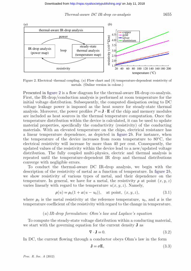
Figure 2. Electrical–thermal coupling. (a) Flow chart and (b) temperature-dependent resistivity ofmetals. (Online version in colour.)
Presented in figure 2 is a flow diagram for the thermal-aware IR-drop co-analysis.First, the IR-drop/conduction analysis is performed at room temperature for theinitial voltage distribution. Subsequently, the computed dissipation owing to DCvoltage leakage power is imposed as the heat source for steady-state thermalanalysis. Moreover, the power profiles P = J · E of the chip and memory modulesare included as heat sources in the thermal temperature computation. Once thetemperature distribution within the device is calculated, it can be used to updatematerial properties, specifically the conductivity (resistivity) of the conductingmaterials. With an elevated temperature on the chips, electrical resistance hasa linear temperature dependence, as depicted in figure 2b. For instance, whenthe temperature of the device increases from room temperature to 80◦C, theelectrical resistivity will increase by more than 40 per cent. Consequently, theupdated values of the resistivity within the device lead to a new/updated voltagedistribution. The fully coupled multi-physics, electric and thermal analysis isrepeated until the temperature-dependent IR drop and thermal distributionsconverge with negligible errors.
To conduct the thermal-aware DC IR-drop analysis, we begin with thedescription of the resistivity of metal as a function of temperature. In figure 2b,we show resistivity of various types of metal, and their dependence on thetemperature. In general, we have for a metal, the resistivity r at point (x , y, z)varies linearly with regard to the temperature u(x , y, z). Namely,
r(u) = r0(1 + a(u − u0)), at point, (x , y, z), (3.1)
where r0 is the metal resistivity at the reference temperature, u0, and a is thetemperature coefficient of the resistivity with regard to the change in temperature.
(a) IR-drop formulation: Ohm’s law and Laplace’s equation
To compute the steady-state voltage distribution within a conducting material,we start with the governing equation for the current density J as
V · J = 0. (3.2)
In DC, the current flowing through a conductor obeys Ohm’s law in the form
J = sE, (3.3)
Proc. R. Soc. A (2012)
on July 11, 2018http://rspa.royalsocietypublishing.org/Downloaded from
1656 Y. Shao et al.
where s is the temperature-dependent electrical conductivity of the conductorsat point (x , y, z). The electric field E can be expressed in terms of the electricpotential f as
E = −Vf, (3.4)
which leads to Laplace’s equation of scalar electric potential. We have
V · sVf = 0, (3.5)
with the boundary conditions
f = fd, on Gd,
svf
vnl= f
RlSl, on Gl, (3.6)
and svf
vnn= 0, on Gn, (3.7)
where Gd is the Dirichlet boundary surface where voltage on it is given, and Glrepresents the impedance boundary surfaces to account for external loads suchas chips and memories. Rl and Sl are the load resistance and cross-sectional areaof Gl, respectively. Finally, Gn denotes the Neumann boundary surface throughwhich no currents are allowed to flow.
The equivalent load resistance Rl is generally also temperature dependent. Forsimplicity, in this work, we treat it as constant and derive it from the powerconsumption in the chip/memory layer under ideal operating condition, namelywithout any IR drop. Hence, for example, with a power consumption of Pl on aload chip, we have
Rl = V 2dd
Pl. (3.8)
Here, we use the supply voltage Vdd to compute the equivalent load impedance Rlon the chips. Owing to the finite resistivity of the metal plane, the actual voltagefvia at the via location will be smaller than Vdd, and subsequently, the amount ofvoltage delivered by the PDN to the chip modules may be insufficient for chipsto function properly.
(b) Decomposed boundary-value problem
Here, we introduce a non-conformal and non-overlapping DDM for the solutionof DC IR-drop analysis. For simplicity, we only decompose the original probleminto two sub-domains. The boundary-value problem (BVP) of IR drop on thePDN for the decomposed problem of figure 3 may then be written as
V · siVfi = 0, in Ui , (3.9)
fi = f(i)d , on G
(i)d , (3.10)
sivfi
vn(i)l
= fi
R(1)l S (i)
l
on G(i)l , (3.11)
Proc. R. Soc. A (2012)
on July 11, 2018http://rspa.royalsocietypublishing.org/Downloaded from

Thermal-aware DC IR-drop co-analysis 1657
nlnl
(1)
nG(2) nG
(1)
nl
nn(1)
nn(2)nl
(2)nn Gn
Gl
Gd
Gl
GdGd
(2)Gd(1)
G l (1)
Gn(1) G12
Gl(2) Gn
(2)
WW1 W2
s (x,y,z)
s1 (x,y,z)
s2 (x,y,z)
Figure 3. Notations for decomposing the original problem domain into two sub-domains. (Onlineversion in colour.)
sivfi
vn(i)n
= 0, on G(i)n , (3.12)
f1 = f2, on G12, (3.13)
and − s1vf1
vn(1)G
= s2vf2
vn(2)G
, on G12. (3.14)
Here, i = 1, 2, and equations (3.13) and (3.14) are interface boundary conditions(transmission conditions) that impose the continuities of voltage f and currents(vf/vn) at the interface G of adjacent sub-domains.
Herein, we adopt a non-conformal DDM approach such that the originalproblem can be divided into a number of sub-domains with smaller sizes, and eachsub-domain can be meshed independently without consideration of conformityto the adjacent sub-domains. The boundary conditions, the continuities of bothvoltage and current across interfaces, will be imposed through the interior penalty(IP) (Arnold 1982; Houston et al. 2005; Rawat 2009) method.
(i) Interior penalty formulation
Regarding the decomposed BVP (3.9)–(3.14), with every trial–function pair,(f1, f2), we have the following residuals:
R(1)Ui
:= V · siVfi , in Ui , (3.15)
R(2)
G(i)l
:= sivfi
vn(i)l
− fi
R(i)l S (i)
l
, on G(i)l , (3.16)
R(3)
G(i)n
:= sivfi
vn(i)n
, on G(i)n , (3.17)
R(4)G12
:= f1 − f2, on G12, (3.18)
and R(5)G12
:= s1vf1
vn(1)G
+ s2vf2
vn(2)G
, on G12. (3.19)
On the Dirichlet surface, G(i)d , i = 1, 2, the Dirichlet boundary conditions fi =
f(i)d shall be enforced strongly as the essential boundary conditions. Namely, the
Proc. R. Soc. A (2012)
on July 11, 2018http://rspa.royalsocietypublishing.org/Downloaded from

1658 Y. Shao et al.
boundary conditions fi = f(i)d on G
(i)d are satisfied exactly and will not result in
any residuals for any trial function in the trial function space.The above residuals can be interpreted as the error sources that support the
differences between the exact voltage distribution and the trial numerical solution.In applying the Galerkin method, we shall test each of these residuals in spatialdomains by test functions in its dual space. For example, the test function for theresidual R(1)
U1needs to be in the Sobolev space (Adams 1975) H 1
0 (U1), the dualspace of H −1(U1). To derive the weak form Galerkin statement, we follow the IPapproach and begin by properly testing each of the residuals in (3.15)–(3.19) bytest functions in its dual space. Following the IP formulation, with proper dualpairing for each of the residuals, we obtain the following weak Galerkin statement.Find (f1, f2) ∈ (H 1
0 (U1) ⊕ H 10 (U2)), such that
2∑i=1
(vi , R(1)Ui
)Ui + c1
2∑i=1
〈vi , R(2)
G(i)l
〉G
(i)l
+ c2
2∑i=1
〈vi , R(3)
G(i)n
〉G
(i)n
+ c3
⟨s1
vv1
vn(1)G
− s2vv2
vn(2)G
, R(4)G12
⟩G12
+ c4〈v1 + v2, R(5)G12
〉G12
+ 〈v1 − v2, p1R(4)G12
〉G12 +⟨
s1vv1
vn(1)G
+ s2vv2
vn(2)G
, p2R(5)G12
⟩G12
= 0,
∀(v1, v2) ∈ (H 10 (U1) ⊕ H 1
0 (U2)), (3.20)
where
(a, b)U :=∫
U
a · b dV (3.21)
and
〈a, b〉G :=∫
G
a · b dS . (3.22)
Moreover, the last two terms on the left-hand side of (3.20), inspired bythe IP methods, are included to penalize the discontinuities of the voltage andthe current across interface G12. We see their importance upon considering theboundary testings⟨
s1vv1
vn(1)G
, c3R(4)G12
+ p2R(5)G12
⟩G12
= 0, ∀v1 ∈ H 10 (U1),⟨
s2vv2
vn(2)G
, −c3R(4)G12
+ p2R(5)G12
⟩G12
= 0, ∀v2 ∈ H 10 (U2),
⎫⎪⎪⎪⎪⎪⎬⎪⎪⎪⎪⎪⎭(3.23)
and〈v1, c4R(5)
G12+ p1R(4)
G12〉G12 = 0, ∀v1 ∈ H 1
0 (U1),
〈v2, c4R(5)G12
− p1R(4)G12
〉G12 = 0, ∀v2 ∈ H 10 (U2).
⎫⎬⎭ (3.24)
Proc. R. Soc. A (2012)
on July 11, 2018http://rspa.royalsocietypublishing.org/Downloaded from

Thermal-aware DC IR-drop co-analysis 1659
The coefficients appearing in (3.23) and (3.24) can be chosen arbitrarily, otherthan zeros, to weakly enforce transmission conditions on the interface betweensub-domains and thereby satisfy (3.13) and (3.14).
(c) Volume penalty terms
We consider the volume penalty terms (vi , R(1)Ui
)Ui , i = 1, 2, in equation (3.20).Through the application of the Green theorem (or integration by parts), theexpression (v1, R(1)
U1)U1 can be re-written as
(v1, R(1)U1
)U1 := −(Vv1, s1Vf1)U1 +⟨v1, s1
vf1
vn(1)l
⟩G
(1)l
+⟨v1, s1
vf1
vn(1)G
⟩G12
+⟨v1, s1
vf1
vn(1)n
⟩G
(1)n
. (3.25)
A similar expression exists for (v2, R(1)U2
)U2 . Introducing a notation (v, R(1)U )U via
(v, R(1)U )U =
2∑i=1
(vi , R(1)Ui
)Ui = a(v, f) + g0〈v, f〉 +⟨v, s
vf
vnl
⟩Gl
+⟨v, s
vf
vnn
⟩Gn
,
(3.26)where
a(v, f) := −2∑
i=1
(Vvi , siVfi)Ui ,
g0〈v, f〉 :=2∑
i=1
⟨vi , si
vfi
vn(i)G
⟩G12
,
⟨v, s
vf
vnl
⟩Gl
:=2∑
i=1
⟨vi , si
vfi
vn(i)l
⟩G
(i)l
and⟨v, s
vf
vnn
⟩Gn
:=2∑
i=1
⟨vi , si
vfi
vn(i)n
⟩G
(i)n
.
⎫⎪⎪⎪⎪⎪⎪⎪⎪⎪⎪⎪⎪⎪⎪⎪⎪⎪⎪⎬⎪⎪⎪⎪⎪⎪⎪⎪⎪⎪⎪⎪⎪⎪⎪⎪⎪⎪⎭
(3.27)
(d) Surface penalty terms
Consider the surface penalty terms in (3.20). In the finite-element formulation,a popular choice is to set c1 = c2 = −1. We shall employ the same values for c1and c2, and have
(v, R(1)U )U −
⟨2∑
i=1
〈vi , R(2)
G(i)l
⟩G
(i)l
−⟨
2∑i=1
〈vi , R(3)
G(i)n
⟩G
(i)n
= a(v, f) + g0〈v, f〉 +⟨v,
f
RlSl
⟩Gl
, (3.28)
Proc. R. Soc. A (2012)
on July 11, 2018http://rspa.royalsocietypublishing.org/Downloaded from

1660 Y. Shao et al.
with ⟨v,
f
RlSl
⟩Gl
=2∑
i=1
⟨vi ,
fi
R(i)l S (i)
l
⟩G
(i)l
. (3.29)
Moreover, we have also used c3 = c4 = 1 and p1 = −s/d, p2 = −d/s in theproposed formulation. From equations (3.23) and (3.24), the correspondingtransmission conditions on G12 are therefore
f1 − dvf1
vn(1)G
= f2 + ds2
s1
vf2
vn(2)G
and f2 − dvf2
vn(2)G
= f1 + ds1
s2
vf1
vn(1)G
⎫⎪⎪⎪⎪⎬⎪⎪⎪⎪⎭ on G12, (3.30)
where d is a non-zero value. In the discretized version, we set d to be themesh size of the discretization to render the formulation coercive (Epshteyn &Riviere 2007). Obviously, the enforcement of the Robin transmission conditionsin (3.30) recovers the original boundary conditions described in (3.13) and (3.14)on the domain interface G12.
Furthermore, we introduce two additional notations to simplify the Galerkinweak statement (3.20). They are
g1〈v, f〉 :=⟨
s1vv1
vn(1)G
, R(4)G12
− d
s1R(5)
G12
⟩G12
+⟨
s2vv2
vn(2)G
, −R(4)G12
− d
s2R(5)
G12
⟩G12
=⟨
s1vv1
vn(1)G
,
(f1 − d
vf1
vn(1)G
)−(
f2 + ds2vf2
s1vn(2)G
)⟩G12
+⟨
s2vv2
vn(2)G
,
(f2 − d
vf2
vn(2)G
)−(
f1 + ds1vf1
s2vn(1)G
)⟩G12
(3.31)
and
g2 〈v, f〉 :=⟨v1, R(5)
G12− s1
dR(4)
G12
⟩G12
+⟨v2, R(5)
G12+ s2
dR(4)
G12
⟩G12
= −s1
d
⟨v1,
(f1 − d
vf1
vn(1)G
)−(
f2 + ds2vf2
s1vn(2)G
)⟩G12
− s2
d
⟨v2,
(f2 − d
vf2
vn(2)G
)−(
f1 + ds1vf1
s2vn(1)G
)⟩G12
. (3.32)
Finally, the Galerkin weak formulation for the general partition of the domainU into M sub-domains can be formally stated as the following. Find f ∈(H 1
0 (U1) ⊕ H 10 (U2) ⊕ · · · ⊕ H 1
0 (UM )), such that
a(v, f) + g0〈v, f〉 + g1〈v, f〉 + g2〈v, f〉 +⟨v,
f
RlSl
⟩Gl
= 0, (3.33)
∀v ∈ H 10 (U1) ⊕ H 1
0 (U2) ⊕ · · · ⊕ H 10 (UM ).
Proc. R. Soc. A (2012)
on July 11, 2018http://rspa.royalsocietypublishing.org/Downloaded from

Thermal-aware DC IR-drop co-analysis 1661
The extensions of g0〈v, f〉, g1〈v, f〉, g2〈v, f〉 and 〈v, f/RlSl〉Gl to general Msub-domains are straightforward, and we shall omit the detailed descriptions here.
(e) Finite-dimensional discretization
The corresponding discrete Galerkin weak statement for (3.33) can bewritten as the following. Find fd ∈ (Vd
1 ⊕ Vd2 ⊕ · · · ⊕ Vd
M ), such that
a(vd, fd) + g0〈vd, fd〉 + g1〈vd, fd〉 + g2〈vd, fd〉 +⟨vd,
fd
RlSl
⟩Gl
= 0, (3.34)
∀vd ∈ (Vd1 ⊕ Vd
2 ⊕ · · · ⊕ VdM ), with the finite-dimensional space Vd
i ⊂ H 10 (Ui). In
our current implementation, Vdi is taken as the finite-dimensional subspace
constructed from Kdi , a tetrahedral mesh of Ui with mesh size d, and the
Lagrangian linear interpolation polynomial within each tetrahedral element.Subsequently, the discrete system (3.34) for M sub-domains can be expressed
as the following matrix form:⎡⎢⎢⎢⎣A1 C12 · · · C1M
C21 A2 · · · C2M
... · · · . . ....
CM1 CM2 · · · AM
⎤⎥⎥⎥⎦⎡⎢⎢⎢⎢⎣
f1
f2
...˜fM
⎤⎥⎥⎥⎥⎦, =
⎡⎢⎢⎢⎣y1
y2
...˜yM
⎤⎥⎥⎥⎦, (3.35)
where
Ai =[AII
i AIBi
ABIi ABB
i + CBBii
], Cij =
[0 00 CBB
ij
], fi =
[fi
I
fiB
]and yi =
[yi
I
yiB
].
(3.36)
In equation (3.35), fi denotes the column-coefficient vector of the restriction ofthe sought-after solution fd in the sub-domain Ud
i . We further partition fi intotwo groups: fi
Iand fi
Bfor the interior and boundary unknowns, respectively.
Moreover, the following expressions correlate the sub-matrices in (3.35) and (3.36)with the discrete Galerkin weak statement in (3.34)
Ai : a(vdi , fd
i ), yi : −⟨vd
i ,fd
i
RlSl
⟩Gl
and CBBij(ji) : g0〈(vd)B, (fd)B〉Gij + g1〈(vd)B, (fd)B〉Gij + g2〈(vd)B, (fd)B〉Gij .
⎫⎪⎬⎪⎭ (3.37)
(f ) Matrix solution procedure
In figure 4, we show pictorially our decomposition of the unknown coefficientsvector, fi , within each sub-domain into two groups: the interior unknowns, fI
iand the boundary unknowns, fB
i . We illustrate our decomposition through a two-dimensional example shown in figure 4. For a triangle of the triangulation, if ithas at least one edge residing on the sub-domain interface Gij , we shall label allthree nodes associated with the triangle as the boundary unknowns. All the rest
Proc. R. Soc. A (2012)
on July 11, 2018http://rspa.royalsocietypublishing.org/Downloaded from

1662 Y. Shao et al.
WjGij
T4
T3
T7
T6interior unknowns f I
T5
T2
T1
T8
Wi
˜interface volume unknowns f B˜
Figure 4. Partitioning of the sub-domain unknowns into interior and boundary unknowns. (Onlineversion in colour.)
nodes inside the sub-domain are, by default, labelled as the interior unknowns.A similar procedure is adopted for the three-dimensional applications.
In this section, we detail our solution procedure based on the DDM. To solve thematrix equation in (3.35), we first apply a block-diagonal preconditioner, which issimilar to the additive Schwarz procedure (Lions 1990; Zhao et al. 2007). We have
M−1Af = M−1y, (3.38)
where
A = M + C =
⎡⎢⎢⎢⎣A1 0 · · · 00 A2 · · · 0... · · · . . .
...0 0 · · · AM
⎤⎥⎥⎥⎦+
⎡⎢⎢⎢⎣0 C12 · · · C1M
C21 0 · · · C2M
... · · · . . ....
CM1 CM2 · · · 0
⎤⎥⎥⎥⎦. (3.39)
The corresponding sub-matrices, and the right-hand sides, can be easily identifiedby comparing equation (3.35) with equation (3.38).
Next, we shall introduce a simple restriction operator, Rm , m = 1, 2, . . . , M .Specifically, we have
Rmfm = fBm . (3.40)
Furthermore, it is easy to show that
A−1i Cij fj = A−1
i CijRTj (Rj fj) = A−1
i CijRTj fB
j . (3.41)
Accordingly, we propose to solve the system matrix equation (3.38) in two steps.
Proc. R. Soc. A (2012)
on July 11, 2018http://rspa.royalsocietypublishing.org/Downloaded from

Thermal-aware DC IR-drop co-analysis 1663
— Solving the surface unknowns. With the help of equation (3.41), it is notdifficult to derive the following matrix equation in terms of only the surfaceunknowns: ⎡⎢⎢⎢⎢⎢⎢⎣
I ¯C12... ¯C1M
¯C21 I · · · ¯C2M
... · · · . . ....
¯CM1¯CM2 · · · I
⎤⎥⎥⎥⎥⎥⎥⎦
⎡⎢⎢⎢⎢⎣fB
1
fB2
...fB
M
⎤⎥⎥⎥⎥⎦=
⎡⎢⎢⎢⎢⎢⎣yB
1
yB2
...
yBM
⎤⎥⎥⎥⎥⎥⎦, (3.42)
with ¯Cij = RiA−1i CijRT
j .— Recovering the sub-domain solutions. Once the surface unknowns, fB
i , i =1, 2, . . . , M , are computed, the interior solution for each sub-domain canbe recovered via
fIi = A−1
i
⎛⎝yi −M∑j =i
CijRTj fB
j
⎞⎠. (3.43)
By following the proposed matrix solution procedure, the construction of thepreconditioner requires the inversion of each diagonal block matrices, namely,A−1
i . In practice, these block matrices can be either factorized in a pre-processingstep or solved via another preconditioned Krylov method (Saad 1981) ateach DDM iteration (inner-loop iteration). In the current implementation, wehave employed the multi-frontal solver (Amestoy et al. 2005) to factorize thesubdomain matrix A−1
i .
(g) DC IR-drop analysis of an IBM package example
A Krylov subspace iterative method, generalized conjugate residual (GCR)(Eisenstat et al. 1983), is adopted for the solution of (3.38). The convergencecriteria for the GCR(10) solver is defined as
e = ||M−1(Af − y)||2||M−1y||2 . (3.44)
In the following numerical studies, we use a relative residue, e = 10−6. Allcomputational statistics are reported using a workstation with two quad-core64 bit Intel Xeon E5520 CPUs and 48 GB of RAM.
For a product-level package model such as the one shown in figure 5, it isvery challenging to perform full-wave DC IR-drop analysis. The first challengearises from its geometrical complexity, which contains tens of thousands of smallentities, such as signal traces, three-dimensional interconnects (through-hole viasand buried vias, solder bumps and bump wires) and metallic power/ground layers.The via holes and other cut-outs on the PDN, which has the potential to induceSwiss cheese effects, are illustrated in figure 6. The IR drop owing to such effectscan greatly compromise the performance of the high-speed IC packages and PCBs.As shown in figure 5, it contains about 40 000 geometrical entities. It will beextremely challenging to generate a mesh of the entire package with all these finefeatures. Secondly, even if such a mesh can be constructed, the resulting degrees
Proc. R. Soc. A (2012)
on July 11, 2018http://rspa.royalsocietypublishing.org/Downloaded from

1664 Y. Shao et al.
10.5 mm
(a)
(b)
16.5
mm
0.732mm
sideview 2
sideview 1
side view 1
side view 2
Figure 5. Views of the simulated IBM package geometry: (a) top view and (b) side view. (Onlineversion in colour.)
xyz
Figure 6. PDN geometry that could cause the Swiss cheese effect. (Online version in colour.)
Proc. R. Soc. A (2012)
on July 11, 2018http://rspa.royalsocietypublishing.org/Downloaded from

Thermal-aware DC IR-drop co-analysis 1665
1
0.1
10–2
10–3
10–4
10–5
10–610 20 30 40 50 60 70 80
iterations
resi
dual
(lo
g)
90 100 110 120
Figure 7. Convergence study using DDM to compute voltage distribution of a product-level three-dimensional IC package. (Online version in colour.)
Table 1. Computation statistics of IR-drop analysis.
model IBM package
d.f. 1 673 027preconditioned set-up time (min.s) 00.28iterations (e = 10−6) 75solution time (min.s) 05.17peak memory usage (GB) 2.5
of freedom (d.f.) will be astronomical. It requires excessive computation time andmemory to simulate this product-level three-dimensional package model usingconventional conformal finite-element analysis.
The proposed non-overlapping, non-conformal DDM addresses the above-mentioned difficulties effectively. For this study, we partitioned the entirepower and ground grids into 149 sub-domains, and each of them is discretizedindependently into a tetrahedral mesh. We may notice in figure 7 that theDDM exhibits fast convergence (75 Krylov iterations are required to convergeto 10−6). The computational statistics of IR-drop analysis of the IBM modelare summarized in table 1. The preconditioner setup time indicates the CPUtime required to factorize the 149 sub-domain matrices. As can be seen fromtable 1, the computation resources (both memory and CPU times) required toanalyse the DC IR drop for this product-level multi-scale IC package example arequite modest.
Figure 8 shows the boundary conditions and the voltage distribution on the toplayer. The results indicate that the left bottom corner of layer 1 will see 28 mVof voltage drop. If the nominal voltage of this rail is 1.0 V, the IR drop is 2.8 percent of nominal. Moreover, the simulated IR drop result on the power grids andon the ground grids of the example are shown in figures 9 and 10, respectively.
Proc. R. Soc. A (2012)
on July 11, 2018http://rspa.royalsocietypublishing.org/Downloaded from

1666 Y. Shao et al.
RLSL
RL= 0.2 W
nf f
f0 = 1V
1.000
(b)(a)
0.99080.98150.97220.9630
D D
s
xf
=
= 0
= 0
y
z
x
y x
xf = 0
yf = 0
yf
s f = 0
Figure 8. IBM package PDN with boundary conditions and voltage distribution on the top plane(unit: V). (a) Boundary conditions and ports and (b) voltage distribution at room temperature.(Online version in colour.)
zyx
1.000
(a) (b)
0.99080.98150.97220.9630
z
yx
Figure 9. Voltage distribution on the power planes of layer 1 and layer 7 (unit: V). (a) Side viewand (b) detailed view. (Online version in colour.)
4. Steady-state thermal formulations
Heat conduction is the process of heat transfer in a given region over time. Thegoverning partial differential equation for the steady-state thermal analysis canbe written as
−V · q ′ + q = 0 in U, (4.1)
where q = qd + qe includes the DC power dissipation qd(= J · E = sE2) and chippower consumption qe generated in the medium. Moreover, q ′ is the flow rate
Proc. R. Soc. A (2012)
on July 11, 2018http://rspa.royalsocietypublishing.org/Downloaded from
Thermal-aware DC IR-drop co-analysis 1667
0.005000.00375
0.00250
0.001250
x
z
y
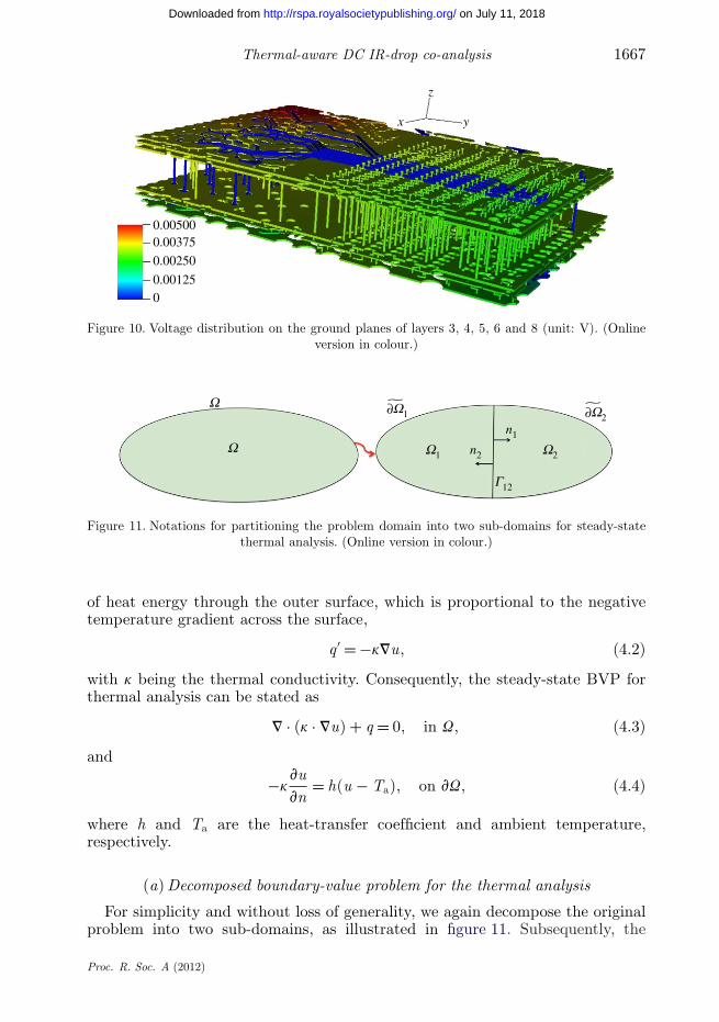
Figure 10. Voltage distribution on the ground planes of layers 3, 4, 5, 6 and 8 (unit: V). (Onlineversion in colour.)
W W1 W2
W2
n2
n1
W
G12
W1
Figure 11. Notations for partitioning the problem domain into two sub-domains for steady-statethermal analysis. (Online version in colour.)
of heat energy through the outer surface, which is proportional to the negativetemperature gradient across the surface,
q ′ = −kVu, (4.2)
with k being the thermal conductivity. Consequently, the steady-state BVP forthermal analysis can be stated as
V · (k · Vu) + q = 0, in U, (4.3)
and
−kvuvn
= h(u − Ta), on vU, (4.4)
where h and Ta are the heat-transfer coefficient and ambient temperature,respectively.
(a) Decomposed boundary-value problem for the thermal analysis
For simplicity and without loss of generality, we again decompose the originalproblem into two sub-domains, as illustrated in figure 11. Subsequently, the
Proc. R. Soc. A (2012)
on July 11, 2018http://rspa.royalsocietypublishing.org/Downloaded from

1668 Y. Shao et al.
decomposed BVP for the steady-state thermal analysis can be written as
V · kiVui + qi = 0, in Ui , (4.5)
u1 = u2, on G12, (4.6)
−k1vu1
vn1= k2
vu2
vn2, on G12, (4.7)
−k1vu1
vn1= h(u1 − Ta), on vU1, (4.8)
and − k2vu2
vn2= h(u2 − Ta), on vU2. (4.9)
Following a similar process as in the non-conformal DDM formulation for IRdrop, the discrete Galerkin weak formulation of the steady-state thermal analysiscan be stated as the following. Find ud ∈ (Vd
1 ⊕ Vd2 ⊕ · · · ⊕ Vd
M ), such that
− (Vvd, kVud)Ud + g0〈vd, ud〉 + g1〈vd, ud〉 + g2〈vd, ud〉− 〈vd, hud〉
vUd + Q(vd) + 〈vd, hTa〉vUd = 0, (4.10)
∀vd ∈ (Vd1 ⊕ Vd
2 ⊕ · · · ⊕ VdM ), where
g0〈v, u〉 :=∑Gij
{〈vi , ki
vui
vni〉Gij + 〈vj , kj
vuj
vnj〉Gij
}, (4.11)
g1〈v, u〉 :=∑Gij
⟨ki
vvi
vni,(
ui − dvui
vni
)−(
uj + dkjvuj
kivnj
)⟩Gij
+∑Gij
⟨kj
vvj
vnj,(
uj − dvuj
vnj
)−(
ui + dkivui
kjvni
)⟩Gij
, (4.12)
g2〈v, u〉 :=∑Gij
−ki
d
⟨vi ,(
ui − dvui
vni
)−(
uj + dkjvuj
kivnj
)⟩Gij
−∑Gij
kj
d
⟨vj ,
(uj − d
vuj
vnj
)−(
ui + dkivui
kjvni
)⟩Gij
(4.13)
and Q(vd) :=∑Ui
(vdi , qi)Ud
i. (4.14)
The discrete system (4.10) results in a matrix equation of the form⎡⎢⎢⎣A1 C12 · · · C1MC21 A2 · · · C2M... · · · . . .
...CM1 CM2 · · · AMM
⎤⎥⎥⎦⎡⎢⎢⎢⎣
u1
u2
...˜uM
⎤⎥⎥⎥⎦=
⎡⎢⎢⎢⎣y1
y2
...˜yM
⎤⎥⎥⎥⎦, (4.15)
Proc. R. Soc. A (2012)
on July 11, 2018http://rspa.royalsocietypublishing.org/Downloaded from

Thermal-aware DC IR-drop co-analysis 1669
with
Ai =[
AIIi AIB
i
ABIi ABB
i + CBBii + DB
i
], Cij =
[0 00 CBB
ij
], ui =
[ui
I
uiB
]and yi =
[yi
I
yiB
].
(4.16)
In equation (4.15), ui denotes the column-coefficient vector of the restrictionof the sought-after solution ud in sub-domain Ud
i . We further partition ui intotwo groups: ui
I and uiB for the interior and boundary unknowns, respectively.
Moreover, the following expressions correlate the sub-matrices in (4.15) and (4.16)with the discrete Galerkin weak statement in (4.10),
Ai : −(Vvdi , kiVud
i )Ui ,
CBBij(ji) : g0〈(vd
i )B,(ud
i )B〉Gij + g1〈(vd
i )B, (ud
i )B〉Gij + g2〈(vd
i )B, (ud
i )B〉Gij ,
DBi : −〈(vd
i )B, h(ud
i )B〉vUi
and yi : −(vdi , q)Ui − 〈(vd
i )B, hTa〉vUi
.
⎫⎪⎪⎪⎪⎪⎬⎪⎪⎪⎪⎪⎭(4.17)
5. Numerical study: thermal-aware IR-drop analysis of printed circuit boardexample
In this section, we will use the power loads at the chip modules as boundaryconditions to obtain a closed-form numerical expression for the voltage profile ofa chip-package-PCB example. IR drop, starting from the power supply source, thevoltage regulator module to the IC circuits, experiences three stages: on-board IRdrop, on-package IR drop and on-chip IR drop. Here, we consider the on-boardIR drop of the PDN of the model. Numerical simulations were conducted on aLinux workstation with two quad-core 64 bit Intel Xeon X5450 CPUs and 48 GBof RAM. All the numerical computations were implemented through the use ofnon-overlapping and non-conformal DDMs, which provide an effective way toalleviate the burden of mesh generation. All the metal layers were fabricated usingcopper with a conductivity of 5.96 × 10⁷ S m−1 at 20◦C. The ambient temperatureat initial iteration is 20◦C. The heat-transfer coefficient between the model andair is 10 W (m2 K)−1.
The computational statistics of the IR-drop analysis of the chip-package-PCB example are summarized in table 2. As seen from figure 12, we observedfast convergence (28 Krylov iterations for IR-drop analysis and 41 iterationsfor steady-state thermal analysis) of the proposed DDM approach. For IR-dropanalysis, when resistivity changed with temperature, the matrix entry on thel.h.s. of equation (3.35) also changes. So, for each thermal-aware IR-drop analysisstep, we need to factorize the sub-domain matrices again.
(a) Example of chip-package-printed circuit board
The PDN in the chip-package-PCB model consists of two parallel copper planesand multiple vias. The vias are not only connected to CPU and RAM, but alsoserved as thermal TSVs, as shown in figure 13. The heat sources of the current
Proc. R. Soc. A (2012)
on July 11, 2018http://rspa.royalsocietypublishing.org/Downloaded from

1670 Y. Shao et al.
1
0.1
10–2
10–3
10–4
10–5
10–6
5 10 15 20 25 30
steady-state thermal analysisIR-drop analysis
35iterations
resi
dual
(lo
g)
40 45 50 55 60
Figure 12. Convergence study to compute voltage and temperature distribution of the chip-package-PCB model. (Online version in colour.)
RAM TSVCPU TSV
12 mm
12 mm
(a)
(b)
xy z
thermal TSV
Figure 13. Chip, memory and thermal TSVs of chip and memory layers: (a) top view and (b) sideview. (Online version in colour.)
Table 2. Computation statistics of thermal-aware IR-drop analysis.
preconditioned solution peakset-up time iterations time memory
analysis d.f. (min.s) (e = 10−6) (min.s) usage (GB)
IR drop 621 380 00.12 28 00.46 0.9steady-state thermal 2 180 529 01.22 41 08.03 4.8
Proc. R. Soc. A (2012)
on July 11, 2018http://rspa.royalsocietypublishing.org/Downloaded from

Thermal-aware DC IR-drop co-analysis 1671
7 WRl = 8.035 W
(a) (b)
(c)
15 WRl = 3.75 W
15 WRl = 3.75 W
7 WRl = 8.035 W
4 WRl = 14.0625W
15 WRl = 18.75 W
4 WRl = 14.0625 W
5 WRl = 11.25 W
7 WRl = 8.035 W
6.5 WRl = 8.654 W
6.5 WRl = 8.654 W
10 WRl = 5.625 W
1.66 WRl = 15.06 W
1.66 WRl = 15.06 W
1.66 WRl = 15.06 W
1.66 WRl = 15.06 W
1.66 WRl = 15.06 W
1.66 WRl = 15.06 W
Figure 14. Volumetric power densities in chip and memory layers: (a) CPU1, (b) CPU2 and(c) RAM1 and RAM2. (Online version in colour.)
xy
(a)(b)
z
Figure 15. Non-conformal partitioning and mesh of the PDN of the chip-package-PCB model. (a)Geometrically non-conformal subdomains and (b) non-matching grids. (Online version in colour.)
study, both on the chip layer, as well as on the memory layer of the stack, areshown in figure 14. The PCB plane in figure 1, with dimensions of 20 × 20 cm,together with the vias, is modelled at room temperature to compute the initial DCIR drop. The entire computational domain is decomposed into 115 sub-domains.Figure 15 shows the geometrically non-conformal sub-domain partitions and non-matching meshes on the sub-domain interfaces.
As shown in figure 16a, 2.5 V is assigned to the top left corner of theplane to mimic the ideal voltage supply. The resulting voltage drop across theplane is shown in figure 16b. In figure 17, the minimum voltage at the chip1module is 2.47172 V, resulting in a maximum voltage drop of 28.28 mV from thepower supply.
Figure 17b illustrates that the hot spot in the temperature profile exists inthe chip1 module, which matches with its power map. After the convergenceof the electrical–thermal co-analysis loop within four iterations (mean squareroot of voltage distribution difference between iterations smaller than 1.0−4),
Proc. R. Soc. A (2012)
on July 11, 2018http://rspa.royalsocietypublishing.org/Downloaded from

1672 Y. Shao et al.
RiSi
Ri
R1 R2R3 R4R5 R6
R7 R8R9 R10R11 R12
U2
Pi
nf f
f0 = 2.5V
(a)(b)
D D
s
xf
=
== 0
chip1module
chip2module
xzy
2.5002.4932.4862.4782.471
xf = 0
yf = 0
xf = 0 s f = 0
Figure 16. Boundary conditions and voltage distribution of the PDN. (a) Boundary conditions and(b) computed initial voltage distribution at room temperature (unit: V). (Online version in colour.)
D Dk u + q = 0
chip1module
·
chip2module
nu = h (u –Ta)
air100.593.0085.50
(b)(a)
77.9970.49
x
yz
k
Figure 17. Boundary conditions and temperature distribution of the chip-package-PCB. (a)Boundary conditions and (b) steady-state temperature distribution (unit: ◦C). (Online versionin colour.)
final voltage distributions compared with the initial voltage profile of the twochip modules are shown in figure 18. The minimum voltage of the two chipmodules with each iteration are illustrated in figure 19. Figure 18 shows thatthe IR drop at every TSV location is increased owing to the Joule heating effecton the PDN. The final voltage distributions of the CPU1 and RAM1 within thechip1 module have maximum IR drops of 34.9 and 33.1 mV, while the initialvoltage distributions have maximum IR drops of 28.28 and 26.9 mV. Moreover,the final voltage distributions of the CPU2 and RAM2 within the chip2 moduleincrease from 22.5 and 22.6 mV to 27.2 and 27.32 mV from the power supply tothe chip2 module, respectively. Compared with the initial IR drop, the final IRdrop increases by about 20 per cent.
6. Conclusion
We propose a multi-physics co-analysis technique to efficiently compute thethermal-aware DC IR drops on the power grid of high-power ICs. The DDM
Proc. R. Soc. A (2012)
on July 11, 2018http://rspa.royalsocietypublishing.org/Downloaded from

Thermal-aware DC IR-drop co-analysis 1673
2.4776
(a) (b)
(c) (d )
2.4745
2.4714
2.4682
2.4776
2.4745
2.4714
2.46822.4651
max: 2.4731min: 2.4716
max: 2.4669min: 2.4651
max: 2.4728min: 2.4727
max: 2.4776min: 2.4775
2.4651
2.4776
2.4745
2.4714
2.4682
2.4651
xy z
xy z
xy z
xy z
2.4776
2.4745
2.4714
2.4682
2.4651
Figure 18. Detailed thermal-aware voltage distributions on the chip modules (unit: V). (a) Initialvoltage distribution of chip1 module; (b) final voltage distribution of chip1 module; (c) initialvoltage distribution of chip2 module; and (d) final voltage distribution of chip2 module. (Onlineversion in colour.)
36
34
32
30
28
26
24
220 1 2
iterations
chip module 1 (CPU1)chip module 1 (RAM1)chip module 1 (CPU2)
chip module 1 (RAM2)
IR d
rop
(V)
3
Figure 19. Maximum thermal-aware IR-drop results with iterations. (Online version in colour.)
Proc. R. Soc. A (2012)
on July 11, 2018http://rspa.royalsocietypublishing.org/Downloaded from

1674 Y. Shao et al.
described herein is a type of non-overlapping and non-conformal DDM, andhence, it is effective in dealing with multi-scale problems. Each sub-region canbe modularly treated in terms of discretization. The use of the proposed DDM isjustified through a practical example of a product-level IC package model and amulti-scale chip-package-PCB example. The thermal-aware DC IR-drop analysisresults demonstrate that owing to the Joule heating of the power grid, the IRdrop may be adversely affected by up to 20 per cent.
The authors would like to thank ANSYS/ANSOFT Corporation for their support on this work.
References
Adams, R. A. 1975 Sobolev spaces. In Pure and applied mathematics, vol. 65. New York, NY:Academic.
Amestoy, P., Duff, I. S. & Voemel, C. 2005 Task scheduling in an asynchronous distributed memorymultifrontal solver. SIAM J. Matrix Anal. Appl. 26, 544–565. (doi:10.1137/S0895479802419877)
Arnold, D. N. 1982 An interior penalty finite element method with discontinuous elements. SIAMJ. Numer. Anal. 19, 742–760. (doi:10.1137/0719052)
Bracken, J. E., Polstyanko, S. V., Pytel, S. G. & Waldron, I. 2011 Coupled thermal–fluid–electricalsimulation for printed circuit board design. In Proc. Int. Conf. on Electromagnetics in AdvancedApplications (ICEAA), Torino, Italy, pp. 1005–1008. Institute of Electrical and ElectronicEngineers (IEEE). (doi:10.1109/ICEAA.2011.6046480)
Eisenstat, S., Elman, H. & Schultz, M. 1983 Variational iterative methods for nonsymmetricsystems of linear equations. SIAM J. Numer. Anal. 20, 345–357. (doi:10.1137/0720023)
Epshteyn, Y. & Riviere, B. 2007 Estimation of penalty parameters for symmetric interior penaltyGalerkin methods. J. Comput. Appl. Math. 207, 843–872. (doi:10.1016/j.cam.2006.08.029)
Farina, D., Hammes, P. & Thoma, P. 2011 Simulation of temperature dependent materialsin high-frequency filters using CST STUDIO SUITEEM 2011. In Proc. Int. Conf. onElectromagnetics in Advanced Applications (ICEAA), Torino, Italy, pp. 1041–1043. IEEE.(doi:10.1109/ICEAA.2011.6046487)
Heinrich, W. 1992 Conductor loss on transmission lines in monolithic microwave and millimeter-wave integrated circuits. Int. J. Microwave Mill 2, 155–167. (doi:10.1002/mmce.4570020304)
Houston, P., Perugia, I., Schneebeli, A. & Schötzau, D. 2005 Interior penalty method forthe indefinite time-harmonic Maxwell equations. Numer. Math. 100, 485–518. (doi:10.1007/s00211-005-0604-7)
Jiang, L., Xu, C., Rubin, B. J., Weger, A. J., Deutsch, A., Smith, H., Caron, A. & Banerjee, K. 2010A thermal simulation process based on electrical modeling for complex interconnect, packaging,and 3DI structures. IEEE Trans. Adv. Pack. 33, 777–786. (doi:10.1109/TADVP.2010.2090348)
Lions, P. L. 1990 On the Schwarz alternating method III: a variant for non-overlapping subdomains.In Proc. 3rd Int. Symposium on Domain Decomposition Methods for Partial DifferentialEquations, Houston, TX, pp. 202–231. Society for Industrial and Applied Mathematics.
Nithin, S. K., Shanmugam, G. & Chandrasekar, S. 2010 3Dynamic voltage (IR) drop analysis anddesign closure: issues and challenges. In Int. Symposium on Quality Electronic Design (ISQED),San Jose, CA, pp. 611–617. IEEE. (doi:10.1109/ISQED.2010.5450515)
Pannikkat, A., Long, J. & Zhao, J. 2004 Power delivery modeling and design methodology for aprogrammable logic device package. In IEEE Conf. Elect. Perform. Electron. Packag. (EPEP),Portland, OR, pp. 115–118. IEEE. (doi:10.1109/EPEP.2004.1407561)
Rawat, V. 2009 Finite element domain decomposition with second order transmission conditionfor time harmonic electromagnetic problem. PhD thesis, Ohio State University, OH, USA.
Saad, Y. 1981 Krylov subspace methods for solving large unsymmetric linear systems. Math. Comp.37, 105–126. (doi:10.1090/S0025-5718-1981-061634-6)
Proc. R. Soc. A (2012)
on July 11, 2018http://rspa.royalsocietypublishing.org/Downloaded from

Thermal-aware DC IR-drop co-analysis 1675
Shao, Y., Peng, Z. & Lee, J.-F. 2010 Full-wave real-life 3-D package signal integrity analysisusing nonconformal domain decomposition method. IEEE Trans. Microw. Theory 59, 230–241.(doi:10.1109/TMTT.2010.2095876)
Shrivastavaa, V., Alurua, N. R. & Mukherjee, S. 2004 Numerical analysis of 3D electrostatics ofdeformable conductors using a Lagrangian approach. Eng. Anal. Bound. Elem. 28, 583–591.(doi:10.1016/j.enganabound.2003.08.004)
Xie, J., Chung, D. Swaminathan, M., Mcallister, M., Deutsch, A., Jiang, L. & Rubin, B. J.2009 Effect of system components on electrical and thermal characteristics for power deliverynetworks in 3D system integration. In IEEE Conf. Elect. Perform. Electron. Packag. (EPEP),Portland, OR, pp. 113–116. IEEE. (doi:10.1109/EPEPS.2009.5338465)
Zhao, K., Rawat, V., Lee, S.-C. & Lee, J.-F. 2007 A domain decomposition method withnonconformal meshes for finite periodic and semi-periodic structures. IEEE Trans. AntennasPropag. 55, 2559–2570. (doi:10.1109/TAP.2007.904107)
Proc. R. Soc. A (2012)
on July 11, 2018http://rspa.royalsocietypublishing.org/Downloaded from


![Thermal-aware job scheduling in data centers [0.2em] An](https://img.dokumen.tips/doc/110x75/62017c32bb030a5ca906db33/thermal-aware-job-scheduling-in-data-centers-02em-an-.jpg)


