Embed Size (px)
Citation preview

Thermal analysis of Printed Circuit Boards for airborne applications
Diana Wilhelmsson
Master of Science Thesis 2017
KTH Industrial Engineering and Management
Machine Design SE-100 44 STOCKHOLM

1
Examensarbete 2017
Termisk analys av kretskort för flygande ändamål
Diana Wilhelmsson
Godkänt
Akademisk handledare
Stefan Wallin
Handledare
Daniel Bengtsson
Uppdragsgivare
SAAB
Kontaktperson
Karin Fröderberg
Sammanfattning
SAAB tar fram och tillverkar kretskort för flygande ändamål. Då kylförsörjningen inte sällan är
begränsad och effektförlusten hög är kretskortens termiska prestanda en viktig parameter att
utvärdera. Detta examensarbete är ett steg i en större utvärdering av de Finita Element Modellerna
(FEM) som används vid termisk analys av korten. Utvärderingen syftar till att skapa större
förståelse för osäkerheter i nuvarande modeller samt att ge nya förslag på hur modellerna kan
förbättras.

2
Master of Science Thesis 2017
Thermal analysis of PCBs for airborne applications
Diana Wilhelmsson
Godkänt
Akademisk handledare
Stefan Wallin
Handledare
Daniel Bengtsson
Uppdragsgivare
SAAB
Kontaktperson
Karin Fröderberg
Abstract Saab develops and manufactures Printed Circuit Board (PCB) for airborne applications. Since the
cooling supply often is limited and power dissipation is high the thermal performance of the PCBs
is an important parameter to evaluate. This thesis is a step in a larger evaluation of the Finite
Element Methods (FEM) used for thermal analysis of the cards. The evaluation aims to create
greater understanding of the uncertainties in current models and to provide new proposals on how
the models can be improved.

3
FOREWORD
During the course of my work, I have been helped by my supervisor Daniel Bengtsson and
colleagues at SAAB and I am incredibly grateful for everything I have learned during this time
and the support. My academic supervisor Stafan Wallin has also been supportive with providing
helpful feedback on my CFD result.
Diana Wilhelmsson
Stockholm, June 2017

4
NOMENCLATURE
Notations
Symbol Description Dimension 𝐴 Area [m2] 𝑑𝑒 Equivalent diameter [m]
𝐶 Specific heat [J/kgK]
𝐶𝑝 Specific heat capacity [J/kgK]
𝐹 Body force [N]
𝑔 Gravitational acceleration [m/s2]
𝐺𝑟 Grashof number -
ℎ Heat transfer coefficient [W/m2K]
𝑘 Thermal conductivity [W/mK] 𝐾 Thermal conductivity [W/mK] 𝐿 Characteristic length [m]
𝑁𝑢 Nusselt number -
n Normal vector -
n Number of moles -
p Pressure [Pa]
𝑃𝑟 Pradtl number -
�̇� Heat flow [W]
�̇� Heat flux [W/m2]
�̇�𝑣 Heat generation [W/m3]
𝑅 Thermal contact resistance [J/molK]
R Universal gas constant [J/W]
𝑆 Surface [m2]
𝑇 Temperature [K]
𝑇 Symmetric tensor -
𝑇𝑏𝑜𝑑𝑦 Body temperature [K]
𝑇∞ Freestream temperature [K]
𝑉 Volume [m3]
𝑥 x- coordinate [m]
𝑦 y- coordinate [m]
𝑧 z- coordinate [m]
𝛽 Volume coefficient of expansion [1/K]
𝛿 Boundary layer thickness [m]
𝜗 Temperature difference [K]
𝜃 Thermal resistance [K/W]
𝜈 Kinematic viscosity [m2/s]
𝜇 Dynamic viscosity [kg/ms]
𝜌 Density [kg/m3]
𝜎 Stefan-Boltzmann’s constant [W/m2K4]

5
𝜆 Equivalent Thermal conductivity [W/mK]
𝜏 Stress tensor [Pa]
Abbreviations
ANSYS Computer Aided Engineering software
BC Boundary Condition
DTM Detailed Thermal Model
CFD Computational Fluid Dynamics
CTM Compact Thermal Model
EWCU Electronic Warfare Central Unit
FEM Finite Element Method
FPGA Field-Programmable Gate Array (integrated circuit)
FVM Finite Volume Method
PCB Printed Circuit Board
SPU Separate Portable Unit
6
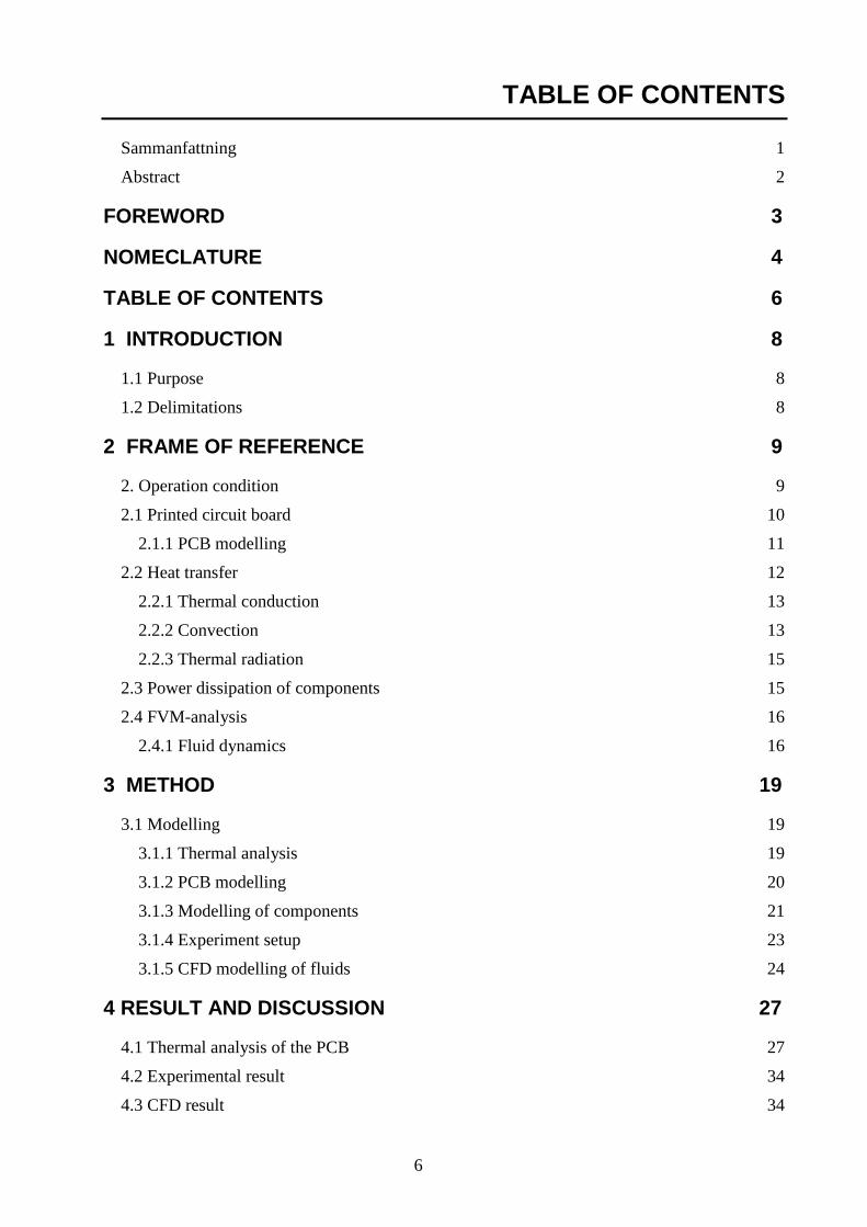
TABLE OF CONTENTS
Sammanfattning 1
Abstract 2
FOREWORD 3
NOMECLATURE 4
TABLE OF CONTENTS 6
1 INTRODUCTION 8
1.1 Purpose 8
1.2 Delimitations 8
2 FRAME OF REFERENCE 9
2. Operation condition 9
2.1 Printed circuit board 10
2.1.1 PCB modelling 11
2.2 Heat transfer 12
2.2.1 Thermal conduction 13
2.2.2 Convection 13
2.2.3 Thermal radiation 15
2.3 Power dissipation of components 15
2.4 FVM-analysis 16
2.4.1 Fluid dynamics 16
3 METHOD 19
3.1 Modelling 19
3.1.1 Thermal analysis 19
3.1.2 PCB modelling 20
3.1.3 Modelling of components 21
3.1.4 Experiment setup 23
3.1.5 CFD modelling of fluids 24
4 RESULT AND DISCUSSION 27
4.1 Thermal analysis of the PCB 27
4.2 Experimental result 34
4.3 CFD result 34

7
5 CONCLUSION 39
6 RECOMMENDATION AND FUTURE WORK 40
7 REFERENCES 41
APPENDIX A: BOARD LEYER SPECIFICATION 43
APPENDIX B: BOARD LAYOUT 44
APPENDIX C: VIA LAYOUT 46
APPENDIX D: GAP PAD POSITION 48
APPENDIX E: POWER DISSIPATION 49
APPENDIX F: POWER DISSIPATION 50
APPENDIX G: THERMAL CONDUCTIVITY 51
APPENDIX H: MATLAB CODE 52
APPENDIX I: INDATA TO MATLAB CODE 55

8
1 INTRODUCTION
1.1 Purpose
Saab develops and manufactures Printed Circuit Boards (PCBs) for airborne applications. Since
the cooling supply often is limited and power dissipation is high the thermal performance of the
PCBs is an important parameter to evaluate. This thesis is a step in a larger evaluation of the Finite
Element Methods (FEM) used for thermal analysis of the cards. The evaluation aims to create
greater understanding of the uncertainties in current models and to provide new proposals on how
the models can be improved.
1.2 Delimitations
There is limitation in the experimental setup and verification of the models due to an uncertainty
of power dissipation of the components on the card.

9
2 FRAME OF REFERENCE
2. Operation condition The Gripen Next Generation has an integrated Electronic Warfare Central Unit (EWCU) which is
located inside the aircraft fuselage. One of the EWCU PCBs will be investigated in terms of
thermal analysis. Figure 1 illustrates the location of the EWCU.
Figure 1. Operation conditions EWCU
EWCU is a closed chassis unit with air cooled edges that has contact with the PCB as seen in
Figure 2. The cooled air will flow inside the wall as the arrows show in the Figure 2 below.
Figure 2. EWCU opened and closed chassis
Due to regulations and lack of space, no fan is allowed in this unit to help the cooling of the PCBs.
Heat generated at the PCBs is transported by conduction towards the air-cooled walls of the
chassis. The same air-cooled principle is used in other systems and applications. As EWCU is a
closed chassis unit the air inside can be expected to be still apart from a small effect from natural
convection from the heated components. In this report, these effects are believed to be very small
and considered as neglectable. The parameters when calculating natural convection are also hard
to estimate and could give a wrong result. The PCB that will be analysed in this report is the third
PCB from the top in Figure 3 of the EWCU.

10
Figure 3. Inside EWCU
2.1 Printed circuit board
Printed circuit boards (PCB) are used in all kinds of electronic applications such as computers, cell
phones, stereos etc.. One of the benefits coming from the usage of PCBs are that the electronic
circuits can be more compact, smaller and placed on an appropriate thin board. The boards
typically consist of an insulating glass epoxy material such as FR-4 with thin layer of copper foil
laminated to one or both sides. Plated holes/vias are drilled down to the desired layer to ensure
connection between the components and to the ground plane. With the through hole technology,
each component has leads that is pushed through holes and soldered to connection pads in the
circuit on the opposite side. Another method which is used is the “surface mounted method” where
the components are connected directly to the printed circuit though J-shaped or L-shaped legs on
the component (How Product are Made 2017).
Figure 4. Through hole device, through hole resistor, surface mounted components (Wikipedia Through hole
technology 2017) (Wikipedia Surface mount Thechnology 2017)
Ball grid array (BGA) surface mounted technology is used for printed circuits with a large number
of pins. The method uses the underside of the package where pins are placed on the underside of
the chip in a grid pattern as seen in the Figure 5 below (Poole 2017).

11
Figure 5. Ball grid array BGA
BGAs are often designed with low thermal resistance upwards so that heat can be transported to
attached heat sinks. Some BGAs also have a thermal pad at the bottom. This thermal pad is
soldered to the PCB facilitating heat transfer in the board direction. Additionally, the balls
themselves contribute to heat transport, foremost those connected to any of the PCBs ground
planes. When thermally modelling a PCB, it is important to understand the mechanism of heat
transfer of the components since they have different impacts on the PCB’s thermal properties, at
least when a simplified PCB model is used. Not all vias contribute to heat transport the same.
Field-Programmable Gate Arrays (FPGAs) are reprogrammable silicon chips (National
Instruments 2017). FPGAs are a combination of the best part of Application- Specific Integrated
Circuits (ASICs) and processor based system. FPGAs don’t need high volumes to provide
hardware speed and reliability like expensive ASIC design. They are also not limited by the
number of processing cores available and are flexible in regards to the software running on a
processor- based system. These components are very popular today and is one of the most
important component in these analysis.
2.1.1 PCB modelling There is a trade-off when it comes to thermal analysis of PCBs. Higher accuracy comes with higher
computational cost. Higher accuracy usually means longer time for the calculations and the
modelling. There are several methods to model PCBs and the importance of having accuracy in
regards to the effort required to gain accuracy needs to be considered. A detailed model can be
used where the physical geometry of the package is reconstructed by integrating mechanical CAD
data for the parts. With the program ANSYS a more complex model could be set up by using the
overall flow in the Figure 6 below (Dillinger 2016).
Figure 6. ANSYS R17.0 workflow (Dillinger 2016)
The RedHawk tool suite generates Chip Power Model (CPM) and Chip Thermal Model (CTM)
abstracts. The SIwave suite has the DC PDN analysis feature which is used to derive the
package/board DC current distribution throughout the plane layers. These currents contribute to
resistive power loses and temperature gradients. A CFD analysis is done by ANSYS Icepak to
determine a complete thermal profile with the help of SIwave DC result for the PDN and the Chip
Thermal Models. The Figure below illustrates how a result from Icepak could look like (Dillinger
2016). As seen in the Figure 7 the result is very detailed.

12
Figure 7.Icepak thermal profile (Dillinger 2016)
A detailed thermal model (DTM) will precisely predict the temperatures of the board. The
temperature in the model can be predicted at several points within the packages including junction,
case and lead temperatures. This type of modelling is appropriate when the number of package is
few due to the high computational time and cost (Advance Thermal Solutions, INC 2017).
In this report, a Compact Thermal Model (CTM) is used where the model aims to predict the
temperature at only the critical points, junction case and leads. This is done using much less
computational effort as the model will not import the correct physical geometry and data. It will
use simplified geometry of the board and the components (Advance Thermal Solutions, INC
2017). In this model, the board material will be homogenized and the components will be modelled
according to the contact are of the board. The model will also use a thermal resistor network such
as the two-resistor model to model the components which is describe in more detailed in the
method section of this report. The two-resistor model is commonly used for CTMs.
2.2 Heat transfer
Heat transfer is related to the first law of thermodynamics which is an equation describing
conservation of energy. The internal energy of a system must be the sum of all input energy and
output energy. Heat transfer occurs when a temperature difference exists within a system or
between systems in thermal contact to each other. The three modes of heat transfer are thermal
conduction, convection and thermal radiation that are illustrated below (Peter von Böckh 2012).
Figure 8. Thermal conduction, convection and thermal radiation
The heat flow/heat rate �̇� is the amount of heat transferred per unit time with the dimension Watt
[W]. The heat flux density �̇� = �̇�/𝐴 is defined as the heat rate per unit area and has the dimension
Watt per square meter [W/m2]. 𝜗 is defined as the temperature.

13
2.2.1 Thermal conduction
Thermal conductivity is a material property and a measure of how well the material can transfer
heat. Heat transfer between a solid wall and a moving fluid develops by the thermal conduction
between the wall and the fluid and within the fluid (Peter von Böckh 2012).
The thermal conductivity constant 𝑘 is determined from Fourier’s law where the heat flux is
proportional to the temperature gradient (Malhammar 2005)
𝜕
𝜕𝑥(𝑘𝑥
𝜕𝜗
𝜕𝑥) +
𝜕
𝜕𝑦(𝑘𝑦
𝜕𝜗
𝜕𝑦) +
𝜕
𝜕𝑧(𝑘𝑧𝜕𝜗
𝜕𝑧) + �̇�𝑣 = 0 (1)
which can be simplified for material that is not coordinate dependant to
𝑘𝑥𝜕2𝜗
𝜕𝑥2+ 𝑘𝑦
𝜕2𝜗
𝜕𝑦2+ 𝑘𝑧
𝜕2𝜗
𝜕𝑧2+ �̇�𝑣 = 0 (2)
and this is sometimes the case for the laminated structures in PCBs. For the case that the thermal
conductivity is the same in all direction equation (1) can be simplified furthermore to
𝐾 (𝜕2𝜗
𝜕𝑥2+𝜕2𝜗
𝜕𝑦2+𝜕2𝜗
𝜕𝑧2) + �̇�𝑣 = 0 (3)
In some more complicated cases the material in electronics like semi-conductors can have
temperature dependant thermal conductivity. For those cases it is more convenient to formulate
equation (1) with the absolute temperature as independent variable according to (Malhammar
2005)
𝐾(𝑇) (𝜕2𝑇
𝜕𝑥2+𝜕2𝑇
𝜕𝑦2+𝜕2𝑇
𝜕𝑧2) + �̇�𝑣 = 0 (4)
2.2.2 Convection
Heat convection is a phenomenon that occurs when heat is moved with the help of fluids. This
movement arises naturally from density variation and with the help of the gravity or could be
forced with the help of for example a fan or a pump. In the natural case an example could be a
heated component that creates density variations within the surrounding fluid as less dense
molecules are formed. The less dense molecules will be rising as they are lighter and the denser
molecules will move down as seen in the left Figure 9 below (Mathematik in den
Naturwissenschaften 2017) (John H. Lienhard IV u.d.).
Figure 9. Natural & forced convection

14
In the right side of Figure 9, a cool gas flows over a warm body and heat is removed trough forced
convection. The fluid next to the body will slow down creating so called boundary layer where
heat is conducted and swept away further downstream where it gets mixed. In this case natural
convection will also be present (John H. Lienhard IV u.d.).
Isaac Newton considered the convective process and suggested that the cooling would be (John H.
Lienhard IV u.d.)
𝑑𝑇𝑏𝑜𝑑𝑦
𝑑𝑡∝ 𝑇𝑏𝑜𝑑𝑦 − 𝑇∞ (5)
and the expression suggests that the energy is flowing from the body. In the expression 𝑇𝑏𝑜𝑑𝑦 is
the body temperature and 𝑇∞ is the temperature of incoming freestream velocity. In the case that
the energy of the body is constantly replenished, the body temperature will not change. Equation
(5) could be reformulated into the basic formulation for deciding the heat transfer coefficient ℎ
(Malhammar 2005)
�̇� = ℎ𝑐𝐴(𝑇𝑏𝑜𝑑𝑦 − 𝑇∞) = ℎ𝑐𝐴𝜗𝑏𝑜𝑑𝑦,∞ (6)
where 𝐴 is the surface area and 𝜗𝑏𝑜𝑑𝑦,∞ is the temperature difference between body and the
freestream.
The heat transfer coefficient ℎ𝑐 for convection is expressed by the Nusselt number Nu (Part B:
Heat Transfer Principals in Electronics Cooling u.d.)
𝑁𝑢 =ℎ𝑐𝐿𝑐𝑘
(7)
where the characteristic length is chosen as the length parameter that has the major impact of the
heat transfer coefficient, see Figure 10 below (Malhammar 2005). The calculation of the heat
transfer coefficient ℎ𝑐 is rather complex as it depends on properties of the fluid and on the flow
itself as well as the surface geometry and in some cases the temperature difference. This report
leaves out a deeper discussion about the calculation of the heat transfer coefficient ℎ𝑐.
For channel flow an equivalent diameter 𝑑𝑒 could be used.
Figure 10. Characteristic lengths Figure 11. PCB
The heat transfer coefficient can be used as a measure of the thermal boundary layer thickness 𝛿
in the case that it is defined as the equivalent thickness of the still fluid layer that has the same
thermal resistance as the heat transfer coefficient (Malhammar 2005)
�̇� = ℎ𝑐𝐴𝜗𝑏𝑜𝑑𝑦,∞ = 𝑘𝐴𝜗𝑏𝑜𝑑𝑦,∞
𝛿 (8)

15
where
𝛿 =𝑘
ℎ (9)
The roughness only has an impact of the heat transfer surface area 𝐴, if it is of the same order of
magnitude as the boundary layer thickness. The roughness on the components can be neglected as
their impact is very small.
2.2.3 Thermal radiation
All bodies with a temperature above absolute zero are continuously emitting electromagnetic
radiation due to the molecular and atomic agitation that is related to their internal energy (Robert
Siegel 2002). Heat transfer through radiation doesn’t need a transfer medium like conduction and
could arise in vacuum and materials that allows the transmission of electromagnetic waves. The
strength of thermal radiation will depend on the temperature of the body and the nature of the
surface. Higher temperature will lead to an increase of thermal radiation and the surface
characteristics will decide if the radiation waves will be fully or partial reflected, transmitted or
absorbed at the surface of the body. A body that absorbs all thermal radiation is called black body
but still emits energy. The Stefan-Boltzmann law describes the black body radiation from a small
surface to an infinitely large surface as (Peter von Böckh 2012)
𝑄12̇ = 𝜎𝐴1(𝑇14 − 𝑇2
4)= 𝜎𝐴1(𝑇12 − 𝑇2
2)(𝑇1 + 𝑇2)(𝑇1 − 𝑇2) (10)
where 𝜎 is the Stefan-Boltzmann’s constant that has fixed value of 5.67 ∙ 10−8 W/m2K4. In the
case that the temperature difference is small equation (10) can be formulated as
𝑄12̇ = 𝜎𝐴14𝑇𝑚3(𝑇1 − 𝑇2) (11)
where 𝑇𝑚 is the average temperature of 𝑇1 and 𝑇2. In this manner, the radiation can be represented
in the same way as the convection in equation (6)
𝑄12̇ = ℎ𝑟𝐴1𝜗12 (12)
2.3 Power dissipation of components
In order to estimate the power dissipation of each components a program is used called XILINK
Power Estimator, UltraScale+TM (XLINK 2017) where the PCB designers insert parameters that
are related to the FPGA components and the critical operating conditions. When the power
dissipation for the FPGA is found, the PCB designer can get the power dissipation for the rest of
the components. The XILINK Power Estimator software estimates the power dissipation of the
FPGA within a range of ±20 %. On top of that there are uncertainties related to operating
temperature, resource utilization, clock rates and toggle rates which all have to be estimated.
After an experiment that was done with the PCB, a new power estimation was found by updating
the operating conditions according to the measurement result. It is assumed that the logic part of
the FPGA power consumption could be neglected (true if loaded heat block code did not execute).
All other components had only half of the power dissipation that was first assumed (hence were
dissipating half of the maximum power dissipation according to the data sheet).

16
2.4 FVM-analysis
Finite Volume Method (FVM) is computational method to solve complex and computational
demanding problems. The basic concept of FVM-analysis is to solve a large problem by dividing
them into smaller finite element. Each element will be described by a set of equations that
approximate a set of partial differential equations. All equations are assembled into a system of
equation that models the large main problem. The partial derivate can be discretized using the
Euler method with respect to time and space.
The partial equation needs to be solved and integrated over all control volumes and is the same as
applying basic conservation laws for each control volume. These is done by an iterative process
due to nonlinearity in the equations. The convergence of the solution will be observed to see that
the solution approaches the exact solution. How correct the final solution is depends on several
factors including the size and shape of the control volume and the residuals (errors).
The analysis in this report is performed using CFX in ANSYS where the discretization option,
High Resolution is chosen. It is a double precision method mixing 2nd and 1nd order accuracy
Upwind discretization scheme to satisfy a boundedness criterion. Problems with robustness is
prevented as the blending function factor decreases where large gradients are present. The method
will try to use the highest order of the scheme as high as possible whilst keeping the solution
bounded everywhere.
2.4.1 Fluid dynamics
The fundamental law of fluid dynamics is described by Navier-Stokes governing equations. The
equation defines the conservation of mass, momentum and energy (Dan S. Henningson and Martin
Berggren 2005). By interpreting Reynolds transport theorem, the equation for conservation of
mass can be derived as
𝜕𝜌
𝜕𝑡⏟1
+𝜕𝜌𝑢𝑘𝜕𝑥𝑘⏟ 2
=𝐷𝜌
𝐷𝑡⏟3
+ 𝜌𝜕𝑢𝑘𝜕𝑥𝑘⏟ 4
= 0 (13)
where 𝜌 is the density of the fluid, 𝑢𝑘 is the velocity, 𝑥𝑘 is the space coordinate and 𝑡 is time. The
first term in the equation refers to the accumulation of mass at a fixed point, the second term refers
to the net flow rate of mass out of the element and the third term refers to the rate of density change
of the material element and the fourth term refers to the volume expansion of the material element.
For incompressible flow 𝜕𝜌
𝜕𝑡= 0 and
𝜕𝜌
𝜕𝑥𝑖= 0 which gives
𝜕𝑢𝑖𝜕𝑥𝑖
= 0 (14)
The principle of conservation of momentum refers to the time rate of change of the momentum in
a material region. By applying Newton´s Law of Motion to a volume of fluid and using the
definition of surface force in terms of stress tensor, the momentum equation is
∫ 𝜌𝐷𝑢𝑖𝐷𝑡
𝑉(𝑡)
𝑑𝑉 = ∫ 𝜌
𝑉(𝑡)
𝐹𝑖𝑑𝑉 + ∫ 𝑇𝑖𝑗𝑆(𝑡)
𝑛𝑗𝑑𝑆 = ∫ [𝜌𝐹𝑖 +𝜕𝑇𝑖𝑗
𝜕𝑥𝑗]
𝑉(𝑡)
𝑑𝑉 (15)
where 𝐹𝑖 is the body force per unit mass, 𝜌 is the density of the fluid, 𝑢𝑖 is the velocity, 𝑥𝑗 is the
space coordinate and 𝑡 is time, 𝑇𝑖𝑗 is a symmetric stress tensor, 𝑆 is surface, 𝑛 is normal and 𝑉 is
volume. By applying that the volume is arbitrary we have following equation

17
𝜌𝐷𝑢𝑖𝐷𝑡= 𝜌𝐹𝑖 +
𝜕𝑇𝑖𝑗
𝜕𝑥𝑗 (16)
and by adding hydrodynamic pressure, 𝑝 (directed inwards) and viscous stress tensor 𝜏𝑖𝑗 (depends
on fluid) we get flowing equation
𝜌𝐷𝑢𝑖𝐷𝑡= −
𝜕𝑝
𝜕𝑥𝑖+ 𝜌𝐹𝑖 +
𝜕𝜏𝑖𝑗
𝜕𝑥𝑗 (17)
𝜕𝑢𝑖𝜕𝑡+ 𝑢𝑗
𝜕𝑢𝑖𝜕𝑥𝑗
= −1
𝜌
𝜕𝑝
𝜕𝑥𝑖+ 𝜈 (
𝜕2𝑢𝑖𝜕𝑥𝑗𝜕𝑥𝑗
) + 𝐹𝑖 (18)
where 𝜈 is the kinematic viscosity.
The energy equation involves the rate of change of energy in a material particle. By including the
energy of the particle, work rate and the heat loss from the surface the equation is
𝜌𝐷𝑒
𝐷𝑡= −𝑝
𝜕𝑢𝑖𝜕𝑥𝑖
+𝜙 +𝜕
𝜕𝑥𝑗(𝑘𝜕𝑇
𝜕𝑥𝑖) (19)
where the last term relates the heat flux to the temperature gradients with Fourier’s Law and where
{
𝜙 = 𝜏𝑖𝑗
𝜕𝑢𝑖𝜕𝑥𝑗
𝜏𝑖𝑗 = 𝜇 (𝜕𝑢𝑖𝜕𝑥𝑗
+𝜕𝑢𝑗
𝜕𝑥𝑖−2𝜕𝑢𝑟3𝜕𝑥𝑟
𝛿𝑖𝑗)
(20)
and where 𝜙 is the positive definite dissipation function and 𝜏𝑖𝑗 gives the relationship between the
viscous stress and the strain (deformation rate) for a Newtonian fluid. The thermodynamics
relation 𝑒 is given by the equation of state for a gas
{𝑒 = 𝑒(𝑇, 𝑃), 𝑒 = 𝑐𝑣𝑇, ℎ = 𝑐𝑝𝑇
𝑝 = 𝜌𝑅𝑇 (21)
where 𝑐𝑝 is the specific heat coefficient depending under constant pressure, 𝑐𝑣 is the specific heat
coefficient under constant volume, 𝜇 is the dynamic viscosity, 𝑘 is the thermal conductivity and 𝑅
is the gas constant.
For the incompressible flow, the energy equation is decoupled from the conservation of mass and
momentum and can be calculated after the flow field is computed. The equation for conservation
of mass no longer involves the time derivate anymore and need a different solution algorithm
(Lecture notes Computational fluid dynamics, KTH u.d.).
Turbulent flow is time-dependent and space-dependent which is identified by random and chaotic
three-dimensional vorticity (CFD online 2017). When the turbulent flow is present an increase in
energy dissipation, heat transfer, mixing and drag is developed. Laminar flow is characterized by
a flow in parallel layers where there is no commotion between them. SST k-ω turbulence model is
a commonly used turbulence model that is a two-equation eddy-viscosity model. The shear stress
transport (SST) k-ω model can use a Low-Re turbulence model without any extra damping factors
as k-ω formulation in the inner boundary layer makes the model directly functioning all the way
down to viscous sub-layer. As the k-ω model is sensitive to the free-stream turbulence properties,
the SST formulation switch to a k-ε behaviour. k-ω model has good behaviour in adverse pressure
gradients and separating flow but could give large turbulence levels in areas with large normal
strain (Davidson 2017). SST k-ω turbulence model is believed to be a reliable turbulence mode

18
and is used at SAAB as standard option due to internal and external high accuracy boundary layer
simulations.

19
3 METHOD
3.1 Modelling
In the first step, two models are compared with a result from a real experiment to find out how
well the model is true to the reality. From that comparison, it is also possible to draw the conclusion
if a more accurate PCB model with local PCB properties represents the reality better and if it is
worth the extra work. In the second step, a CFD model is set up in order to investigate how an
imaginary internal fan in the EWCU would effect the temperature distribution on the SPU board.
3.1.1 Thermal analysis
The computational model is done with CFX in ANSYS 17.1.0. The computational grid consists of
tetrahedral meshes produced by the software. A mesh study of number of layers on the board was
done to ensure a stable solution that is not effected by the mesh. The cell counts and simulation
setup are displayed in the Figure 12 and Table 1-5 below. The analysis is treated as a steady state,
conduction-only problem. Any heat transfer between components and surrounding air is neglected
including radiation. Convective heat transfer between the SPU and surrounding air is also
neglected. Two models will be analyzed, one with homogenized board material and the other one
with homogenized board material and local PCB properties. The thermal conductivity for the
board for each case is seen in Table 3.
Figure 12. Modell setup
Table 1. Model setup
Edge 1 (BC) 47,7 °C
Edge 2 (BC) 44,3 °C
Power dissipation of each component Appendix E
Table 2. Cell counts for the simulation
Region Cells
Solids 2573083

20
Table 3. Material data
Part Material Thermal
conductivity
[W/mK]
Thermal
resistance
[Wm/K]
Mechanic Aluminium 6082 894,0 -
Thermal conductivity
PCB xy-direction
Homogenized board
material (Cu, FR4)
76,5 -
Thermal conductivity
PCB z-direction
Homogenized board
material (Cu, FR4)
3,5 -
Thermal conductivity
PCB xy-direction
Homogenized board
material (Cu, FR4) with
local PCB properties
75,4 -
Thermal conductivity
PCB z-direction
Homogenized board
material (Cu, FR4) with
local PCB properties
2,4 -
Thermal conductivity
under each
component xy-
direction
Homogenized board
material (Cu, FR4) with
local PCB properties
Appendix G -
Thermal conductivity
under each
component z-
direction
Homogenized board
material (Cu, FR4) with
local PCB properties
Appendix G -
Components - 1000,0 -
Gap pads TGF-ZP-SI - 4,9
3.1.2 PCB modelling
The first step in the PCB modelling is to homogenize the board material and calculate an equivalent
conductivity constant for the z-direction and xy-direction. The thermal conductivity for each board
material is given in Table 4 below from material data in (Malhammar 2005).
Table 4. Thermal conductivity for board material
Material Density
[kg/m3]
Thermal conductivity
[W/mK]
Specific heat
[J/KgK]
Copper (Cu), 𝜆𝑐𝑢 8900 380 385
Epoxy, 𝜆𝑒𝑝𝑜𝑥𝑦 1900 0,23 1200
For given board layer specification and board layout in Appendix A and B the thermal conductivity
was derived as following for the z-direction
𝜆𝑧 =𝐴𝑣𝑖𝑎𝑠
𝐴𝑏𝑜𝑎𝑟𝑑𝑛𝑜𝑣𝑖𝑎𝑠𝜆𝑐𝑢 + 𝜆𝑒𝑝𝑜𝑥𝑦 (22)
where 𝐴𝑣𝑖𝑎𝑠 is the total area for the plated thermal vias and 𝐴𝑏𝑜𝑎𝑟𝑑𝑛𝑜𝑣𝑖𝑎𝑠 is the board area excluding
the vias.
For the xy-direction
𝜆𝑥𝑦 =∑𝜆𝑠𝑒𝑘𝑣𝑖+𝜆𝑒𝑝𝑜𝑥𝑦𝑡𝑏𝑜𝑎𝑟𝑑
∑𝑠𝑒𝑘𝑣𝑖+
𝐴𝑣𝑖𝑎𝑠
𝐴𝑏𝑜𝑎𝑟𝑑𝑛𝑜𝑣𝑖𝑎𝑠𝜆𝑐𝑢 (23)

21
where 𝑠𝑒𝑘𝑣𝑖 correspond to the board layer thickness and 𝑡𝑏𝑜𝑎𝑟𝑑 correspond to the thickness that
needs to be added of the epoxy board material to reach the final thickness of the board according
to appendix A.
In the second stage, local PCB characteristics was added where high via concentration are located
on the board. These areas are located under each component and where the board has contact with
the mechanical part at the card edges. In Appendix C these areas are marked in red and is where
the number of thermal vias needs to be calculated. The number of thermal vias are calculated for
BGA components by the number of vias that has the prefix GND that is associated to the
components in the IPC356 file. IPC356 file format is a netlist format includes information about
the PCB such as vias and its coordinates on the board (Nedbal 2017). The format is commonly
used between the board designer and the manufacturer for verification. Components with a thermal
pad underneath each hole needs to be calculated by hand as in Figure 15. For components that has
a thermal pad underneath and also has legs attached to it the calculation of the thermal vias is done
by hand including vias associated to the components in the IPC file.
Figure 13. BGA component Figure 14. BGA
component with GND
vias
Figure 15. Thermal pad
component
Figure 16. Thermal pad
component
The heat transfer coefficient between the edge of the PCB and the rig comes from a wedge lock
study at SAAB and is set to be 1/4581,83 m2K/W (Stigsson 2014). The interface between the
mechanical part and PCB has a thermal resistance of 0,0001 m2K/W which comes from a study
done by Anders Åström at SAAB (Åström 2012).
3.1.3 Modelling of components
All components are modelled as blocks corresponding to the external dimensions of the package.
The board layout can be seen in Appendix C. Highlighted components have gap pads mounted
between the component top and the aluminum carrier. These components are represented by a
JEDEC two-resistor thermal model (STANDARD July 2008). Thermal resistances are applied at
the interface between the component and the board as well as between the component top and the
gap pads. The Figure below illustrates how the model uses the two resistances, junction to top
𝜃𝐽𝐶𝑡𝑜𝑝 and junction to board 𝜃𝐽𝐵 from the component data sheet. As seen in the Figure the interface
(contact area) between the top side of the component and the gap pad will have a resistance 𝜃𝐽𝐶𝑡𝑜𝑝.
The interface (contact area) between the bottom side of the component and the PCB will have a
resistance of 𝜃𝐽𝐵. For the component model described in this thesis the PCB part is excluded,
hence, 𝜃𝐽𝐵 is replaced with 𝜃𝐽𝐶𝑏𝑜𝑡𝑡𝑜𝑚.

22
Data for the resistance for each component is provided from the manufactures and shown in the
Table 5 below.
Table 5. Thermal resistance for the components
Component 𝜃𝐽𝐶𝑡𝑜𝑝
[K/W]
𝜃𝐽𝐶𝑏𝑜𝑡𝑡𝑜𝑚
[K/W]
Contact area
[m2] 𝑅𝐽𝐶𝑡𝑜𝑝
[K m2/W]
𝑅𝐽𝐶𝑏𝑜𝑡𝑡𝑜𝑚
[K m2/W]
U14/U24
(Texas
Instrument
2018)
15,4 0,8 0,00004389 0,000676 0,000351
U16/U18
(Multicore
Fixed and
Floating-Point
Digital Signal
Processor,
TMS320C6678
2017)
0,18 0,18 0,00058081 0,000104546 0,000104546
U36/U56 (Dual
18A or Single
36A , 1/1301-
RYTM9130052
en Rev.A,
LTM4630 u.d.)
1,5 3,7 0,000256 0,000384 0,0009472
U42
(FFVA1156
Flip-Chip,
Fine-Pitch
BGA 2017)
0,06 0,06 0,00225625 0,000135375 0,000135375
Gaps pads are represented by local blocks with a thickness corresponding to the compressed gap
pad height of 0,9 mm. The thermal conductivity of the gap pads are set to be 4,9 W/mK and is
determined from experimental data from a previous study conducted at Saab (Lewin 2015). The
material of the components are modelled to have a high thermal conductivity of 1000 W/mK.
All active components with power dissipation above zero are included in the model.
Figure 17. Two-Resistor Compact Thermal Model (STANDARD July 2008)

23
3.1.4 Experiment setup
In order to get a good test result that could be compared to the model, several thermal probes were
mounted to the PCB, the mechanical part and to the rig as seen in the Figures 18-21 below. The
result from thermal measure points was registered and monitored on the lab computer. The PCB
was mounted to the rig and connected to a voltage sensor as seen in Figure 18.
Figure 18. Test setup Figure 19. Inside of
mechanical part
The thermal measurement probes that were mounted to the PCB were positioned such way that
the hot spots and large thermal gradients would be captured. Probes were positioned on the PCB
primary as well as secondary side. Test point 8-11 was placed to see how the temperature is
distributed over the board in the PCB material to verify how well temperature gradients across the
board are modelled. To verify the thermal conductivity throughout the board is correct, measure
points 16 and 6 were place underneath measure point 8 and 9. Measurement point 7 was placed to
ensure that the thermal interface between the mechanical part and PCB are modelled correct. In
close proximity to this measurement point but on the PCB is measurement point 11.
Figure 20. Measurement points frontside of PCB Figure 21. Measurement poinst backsside of PCB
A summery of all the thermal measurment point is displayed below.

24
Table 6. Thermal measurement point
1) PCB frontside, underneath U42 9) PCB frontside, board above U33
2) PCB backside, U43 10) PCB frontside, board left side P8
3) PCB backside, U10 11) PCB frontside, board right side P10
(interface mechanical part)
4) PCB backside, U41 12) PCB backside, U42
5) PCB backside, U14 13) Edge 1
6) PCB backside, board above U43 14) Edge 2
7) Inside mechanical part, Interface between
board and mechanical part
15) Middle of the mechanics
8) PCB frontside, board above U42 16) PCB backside, board above U33
ZYNG) Junction temperature U43 FPGA) Junction temperature U42
3.1.5 CFD modelling of fluids
As an experiment to investigate the effect that an imaginary internal fan in the EWCU would have
on the temperature distribution on the SPU board, a simple fluid model was set up. The Figure 22
below illustrates the control volume that will be used which is only the SPU board and the volume
to the next PCB. Two cases will be modelled with CFX in ANSYS version 17.1.0 with the same
conditions but one with a fan and one without a fan. The computational grid consists of tetrahedral
meshes produced by the software. For the fan case, a mesh study of boundary layer mesh of the
fluid was first done to verify that it was correctly resolved. The cell counts for the analysed region
is displayed in Table 8. The Cell count for the case without fan will only have the solid part in the
analysis.
Figure 22. Modelling setup for the fan case

25
Figure 23. Modelling setup for the case without the fan
The conditions for the analysis are displayed in the Table 7-10 below.
Table 7. Model setup
Inlet velocity (BC) 1 m/s
Inlet temperature (BC) 60°C
Outlet pressure (BC) 0 Pa
Surface area (fluid) Adiabatic wall
Edge 1 and 2 (BC) 60 °C (An approximation of average air
temperature in EWCU is used)
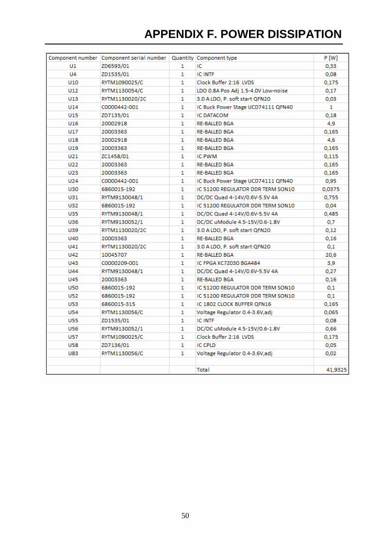
Power dissipation of each component Appendix F
Turbulence model k-ω SST (shear stress transport) with y+ wall
treatment
Table 8. Cell counts for the simulation
Region Cells
Fluid 6520511
Solids 4341083
Total 10861594
Table 9. Material data
Part Material Thermal
conductivity
[W/mK]
Thermal
resistance
[W/mK]
Rig (Edge 1-2) Aluminium 6082 894 -
Mechanic Aluminium 6082 894 -
Thermal conductivity
PCB xy-direction
Homogenized board
material (Cu, FR4)
76,5 -
Thermal conductivity
PCB z-direction
Homogenized board
material (Cu, FR4)
3,5 -
Components - 1000 -
Gap pads TGF-ZP-SI 4.9 4,9
Support box adjacent
to the PCB
Plastic material
(Polymer)
0,17 -

26
Table 10. Fluid properties used in the analysis of the fan case
Part Material Thermal
conductivity at
60 °C [W/mK]
Kinematic
viscosity at
60 °C
[m2/s]]
Density at
60 °C
[kg/m3]
Specific heat
capacity at 60 °C
[J/kgK]
Fluid (The
Engineering
ToolBox
2017)
Air 0,0285 18,90 1,067 1,009

27
4 RESULT AND DISCUSSION
4.1 Thermal analysis of the PCB
Result from the mesh study indicated that board should be divided into three layers to obtain a
good result. In the Figure 24 below three measurement points were observed and three cases were
compared. In the three cases, the element size of the body sizing of the board was changed
according to total board thickness divided by 2,3 and 4.
Figure 24. Body sizing
When analysing the two models (homogenized board material and homogenized board material
with local PCB properties, one should keep in mind the result of the thermal conductivity for the
board as seen in the Table 11 below. Conclusions that could be drawn from that is that the model
with local PCB properties have less thermal conductivity properties over and through the board
where local material properties are not present under the components.
Table 11. Thermal conductivity of the board for the models
Thermal conductivity
[W/mK]
Homogenized board
material
[W/mK]
Homogenized board
material with local PCB
properties
[W/mK]
xy-direction 76,5 75,4
z-direction 3,5 2,4
Temperature plots from the two models are displayed below where it is seen in that the model with
local PCB properties have higher temperatures (Figure 26,28,30).
In the Table 12 below the same measurement points are compared that is discussed in
“Experimental setup” where the two models are compared. The temperature difference is defined
as Thomogenized PCB- Tlocal PCB properties.
351,91 351,61 351,36
356,39 356,27 356,12
361,72 361,5 361,49
345
350
355
360
365
n=2 n=3 n=4
Tem
per
atu
re [
K]
Body sizing (element size) (Total thickness/n) [mm]

28
Table 12. Temperature differences between the two models
The comparison of the models shows that the result for the two FPGA components (ZYNG(U43),
FPGA(U42)) have a small discrepancy of maximum 1,1 degrees. The result in the other
measurement points have also small discrepancies which indicates that these models do not have
big differences in the result. The biggest difference is located at measurement point 11 where the
model with the homogenized board material is warmer (approximately 3°C).
In the Figures 25-30 below it is seen that hot spots are present in the regions were the components
with the highest power dissipation is located. The maximum temperature for the front and back
side of the PCB for the model with homogenized board material is 69,7 °C and for the model with
local PCB properties 70,8 °C. The minimum temperature for the model with homogenized board
material is 46,8 °C and for the model with local PCB properties 48,8 °C.

29
Figure 25. Front side homogenized board material
Figure 26. Front side homogenized board material with local PCB properties
By observing the Figures 27-28 for the back side of the PCB one can see that heat is more spread
out in the hot spots region for the homogenized board material. This is expected as the thermal
conductivity is higher in the xy-direction for the board material. For the model with local PCB
properties the small FPGA component (ZYNG/U43) have two effects present as the material
property have little higher conductivity in z-direction (75,4 W/mK) and lower thermal conductivity
(2,4 W/mK) than the board material. These facts can be the reason that the hot spot is more centred.

30
Figure 27. Back side homogenized board material
Figure 28. Back side homogenized board material with local PCB properties

31
Figure 29. Mechanical part homogenized board material
Figure 30. Mechanical part homogenized board material with local PCB properties
The tables 13-14 below shows a comparison between the two models for each measurement points
discussed in the “Experimental setup”. The temperature difference is defined as
Texperiment- Tmodel.
The measurement points in Table 13 for the model with homogenized board material shows a
maximum measurement error of 7,15°C for the junction temperature for the FPGA component.
The probes on the PCB and mechanics have maximum measurement error of 5,5 °C.

32
Table 13. Measurement point result for the model with homogenized PCB material
As seen in Table 14 below for the model with local PCB properties is that the junction temperature
for the big FPGA (U42) component (measurement point FPGA) is too low (6,95 °C), the
temperature underneath the components (measurement point 2) is too high (4,95 °C) and the region
close to the component (measurement point 1) is also to high (5,299 °C). This indicates that the
resistance between junction and PCB are modelled to low or that the model of the component
(represented as a block) is too simple. For the smaller FPGA component (U43) is the junction
temperature (measurement point ZYNG) too low (3,55 °C) and the temperature underneath
(measurement point 12) is too high (7,35 °C). This also indicates that the resistance between
junction and PCB are modelled too low.

33
Table 14. Measurement point result for the model with local PCB properties
In order to verify the thermal conductivity in the xy-direction, the temperature difference between
measurement point 8 and 11 is calculated. The temperature difference from the experiment is 11,6
°C, the model with homogenizer PCB material only has a temperature difference of 13,098 °C and
the model with local PCB properties has a temperature difference of 16,36 °C. This indicates that
we do not have hotspots as we modelled and that heat is transferred much easier than modelled.
One reason could be that in the reality the heat goes easier up from the component to the
mechanical part. The temperature of the mechanics is modelled high and largely follows the highly
modeled PCB temperatures.
For the verification of the thermal conductivity in the z-direction the temperature difference of the
measurement 6-9 and 16-8 was calculated for both model and experiment result. The result was
different in both cases and no conclusion can be drawn from that.

34
4.2 Experimental result
During the experiment, the total power dissipation of the PCB was measured to be 40,987 W which
is almost 50% of the maximum calculated power dissipation (81,895W) that was first given from
the PCB designer.
Table 15. Result from the thermal measurement points
1) 59,3 °C 9) 58,2 °C
2) 60,7 °C 10) 53,54 °C
3) 58,9 °C 11) 47,9 °C
4) 55,5 °C 12) 60,7 °C
5) 52,5 °C 13) 47,7 °C
6) 58,7 °C 14) 44,3 °C
7) 47,2 °C 15) 57,1 °C
8) 59,5 °C 16) 57,5 °C
ZYNG) 74,3°C FPGA) 73,1°C
4.3 CFD result
The result from the mesh study of the fluid indicates that the number of element and the grows
size of the inflation layer covers the boundary layer of the flow. An average temperature of the
outlet for three different mesh sizes gave same result of 61,75 °C.
Figure 31. Boundary layer
The Figures 32-33 below show the temperature difference of the PCB on the front side. The
temperatures for the fan case are between 65,0°C and 88,2 °C and for the non fan case between
63,6 °C and 89,2 °C. As seen in the Figure 33,35,37 for the fan case is that the air contributes to a
spreading of the heat over the board which also only provides a small cooling effect. By adding a
fan the coldest part of the PCB has higher temperatures and the highest temperature is lower which
was expected

35
Figure 32. Front side PCB (No fan)
Figure 33. Front side PCB (Fan)
The Figures 34-35 below show the temperature difference of the PCB on the back side. The
temperatures for the fan case is between 65,0 °C and 88,2 °C and for the non fan case between
63,6 °C and 89,2°C. The highest temperature hotspots are present for the non fan case in Figure
34 and gets its behaviour from the fact that the thermal conductivity is much higher in z- direction
(76,47 W/mK) than the xy-direction (3,48 W/mK).

36
Figure 34. Back side PCB (No fan)
Figure 35. Back side PCB (Fan)
The Figures 36-37 below shows the temperature difference of the mechanics. The temperatures
for the non fan case is between 60,5°C and 84,8°C and for the fan case 62,5°C and 86,0°C.

37
Figure 36. Mechanics (No fan)
Figure 37. Mechanics (Fan)
The Figure 38 below shows the temperature distribution of the air around the SPU card. The air
temperature is between 60,0°C and 67,4°C. The average outlet temperatures are 61,6°C and 61,7°C
which indicates that the airflow transports energy out as the inlet temperature is 60°C.

38
Figure 38. Temperature distribution of the air (Fan)
The velocity distribution of the air is seen in Figure 39 below. It is seen that velocity goes up in
the area close to the outlet. In the clear blue regions, the velocity is zero or close to zero.
Figure 39. Velocity distribution of the air (Fan)

39
5 CONCLUSION
There is an uncertainty in the models as the experiment indicates that the first ansatz of the total
power dissipation of the PCB was over estimated. The benefits of modelling the PCB with local
material properties does not give a significant better result and the focus in the future should be to
gain better knowledge of the power dissipation of each component. Both models indicated that the
FPGAs are modelled too cold which could lead to a catastrophic event when the components are
heavily loaded in a real situation. Therefore, when modelling FPGAs a more detailed model of the
component should be used.
The result by adding a fan that will circulate the air around the PCB contributes to a small cooling
effect of the PCB. If the inlet temperature of the fan would be less it would increase the cooling
effect. In order to investigate this further the whole EWCU should be considered and also with the
different temperature gradients in the wall of the EWCU. The wall will be coldest close to where
the air enters the wall and warmest where the air leaves the wall.

40
6 RECOMMENDATIONS AND FUTURE WORK
In order to evaluate the models correct the best solution would be to use a PCB where it is possible
to measure the real power dissipation of each component. In that case the verification of the model
would be more correct and not dependent on estimating power dissipation.
The FPGAs have a significant impact on the heat distribution of the PCB and therefore needs to
be modelled right and more studies of these kind would be beneficial.
A recommendation is to initiate a follow up and keep statistics for the power dissipation for more
PCB cards.

41
7 REFERENCES
“How Product are Made 2017”, 09 05 2017.
http://www.madehow.com/Volume-2/Printed-Circuit-Board.html.
"Wikipedia Through hole technology 2017",09 05 2017.
https://en.wikipedia.org/wiki/Through-hole_technology.
"Wikipedia Surface mount Thechnology 2017", den 09 05 2017.
https://en.wikipedia.org/wiki/Surface-mount_technology.
"Poole 2017", 12 05 2017.
http://www.radio-electronics.com/info/data/smt/smd-bga-ball-grid-array-package.php.
"National Instruments 2017", 07 07 2017
http://www.ni.com/white-paper/6983/en/
"Dillinger 2016", 10 02 2016
Dillinger, Tom. The Open Forum for Semicoductor Professionals.
https://www.semiwiki.com/forum/content/5473-early-structural-reliability-analysis-chip-
package-system-design-must.html.
"Advance Thermal Solutions, INC 2017"
Strategies for CFD Modeling of Complex PCBs. 22 06 2017.
https://www.google.se/url?sa=t&rct=j&q=&esrc=s&source=web&cd=1&ved=0ahUKEw
iZk83cmtLUAhUlCpoKHeTxC_UQFggpMAA&url=http%3A%2F%2Fwww.qats.com%
2FDownload%2FQpedia_Oct10_Strategies_for_CFD_modeling_of_complex_PCBs.ashx
&usg=AFQjCNGFEdu7SRqRjU76UsPMyxGMopGl7w
"Peter von Böckh 2012"
Peter von Böckh, Tjomas Wetzel. Heat Transfer. Verlag Berlin Heidelberg: Springer,
2012.
"XLINK 2017", 07 07 2017
https://www.xilinx.com/products/technology/power/xpe.html
"Mathematik in den Naturwissenschaften 2017", 06 03 2017.
http://www.mis.mpg.de/applan/research/rayleigh.html.
"John H. Lienhard IV u.d."
A heat transfer textbook, Fourth edition. Cambridge Massachusetts: Phlogiston press,u.d.
"Part B: Heat Transfer Principals in Electronics Cooling" .
Cario : Cario university faculity of engineering, u.d.
"Malhammar 2005"
Malhammar, Åke. Thermal Design for Electronics. 2005.
"Robert Siegel 2002"
Robert Siegel, John R. Howell. Thermal Radiation Heat Transfer, Fourth Edition.
London: Taylor & Francis, 2002.
"Dan S. Henningson and Martin Berggren 2005"
Dan S. Henningson, Martin Berggren. Fluid Dynamics:Theory and Computation.
Department of Mechanics and the department of Numerical Analysis and Computer
Science, KTH, Stockholm: August 24, 2005.
"Lecture notes Computational fluid dynamics, KTH u.d", 29 06 2017
https://www.kth.se/social/files/58acb076f27654686565dd3a/FV_discretization.pdf
"CFD online 2017",29 06 2017. Martin Berggren.
https://www.cfd-
online.com/Wiki/Introduction_to_turbulence/Nature_of_turbulence#What_is_turbulence.
3F.

42
"Davidson 2017"
Davidson, Lars. Fluid mechanics, turbulent flow and turbulence modelin. Göteborg,
Sweden: Division of Fluid Dynamics, Department of Applied Mechanics Chalmers
University of Technology , 2017.
"Nedbal 2017", 22 05 2017
Nedbal, Rich. ”DownStream Technologies.” den. http://www.downstreamtech.com/cam-
advisories/IPCD356_Simplified.pdf.
"Stigsson 2014"
Stigsson, Per. TP-20009035 . Järfälla, Stockholm: SAAB, 2014.
"Åström 2012"
Åström, Anders. BORE2, utvärdering av beräknande och provande resultat. Järfälla,
Stockholm: SAAB, 2012.
"STANDARD July 2008"
STANDARD, JEDEC. Two-Resistor Compact Thermal Model Guideline, JESD15-3.
Virginia: JEDEC SOLID STATE TECHNOLOGY, July 2008.
"Texas Instrument 2018", 12 06 2017
High-Current, Synchronous Buck Power Stage, 1/1301-C0000442 en Rev. A.
www.ti.com.
"Multicore Fixed and Floating-Point Digital Signal Processor, TMS320C6678 2017",
12 06 2017. www.ti.com.
”Dual 18A or Single 36A , 1/1301-RYTM9130052 en Rev.A, LTM4630.”
Linear Technology. u.d. www.linear.com/LTM4630.
”FFVA1156 Flip-Chip, Fine-Pitch BGA.”
XILINX. den 12 06 2017. www.xilinx.com.
"Lewin 2015"
Lewin, Susanne. M-10045244. Järfälla, Stockholm: SAAB, 2015.
"The Engineering ToolBox 2017", 28 06 2017
http://www.engineeringtoolbox.com/air-properties-d_156.html.

43
APPENDIX A. BOARD LAYER SPECIFICATION

44
APPENDIX B. BOARD LAYOUT

45
APPENDIX B. BOARD LAYOUT

46
APPENDIX C. VIA LAYOUT

47
APPENDIX C. VIA LAYOUT

48
APPENDIX D. GAP PAD POSITION

49
APPENDIX E. POWER DISSIPATION
50
APPENDIX F. POWER DISSIPATION

51
APPENDIX G. THERMAL CONDUCTIVITY
52
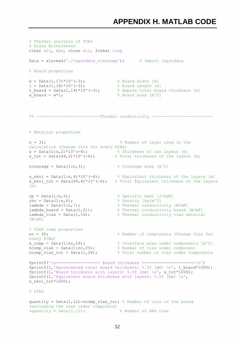
APPENDIX H. MATLAB CODE
% Thermal analysis of PCBs % Diana Wilhelmsson clear all, clc, close all, format long
Data = xlsread('./inputdata_viascomp'); % Import inputdata
% Board properties
w = Data(1,17)*10^(-3); % Board width [m] l = Data(1,18)*10^(-3); % Board length [m] t_board = Data(1,19)*10^(-3); % Approx total board thickness [m] a_board = w*l; % Board area [m^2]
%% --------------------------Thermal conductivity -------------------------
% Material properties
n = 31; % Number of layer used in the
calculation (Change this for every PCBs) s = Data(1:n,2)*10^(-6); % Thickness of the layers [m] s_tot = Data(49,2)*10^(-6); % Total thickness of the layers [m]
covarage = Data(1:n,3); % Coverage area [m^2]
s_ekvi = Data(1:n,4)*10^(-6); % Equivalent thickness of the layers [m] s_ekvi_tot = Data(49,4)*10^(-6); % Total Equivalent thickness of the layers
[m]
cp = Data(1:n,5); % Specific heat [J/kgK] rho = Data(1:n,6); % Density [kg/m^3] lambda = Data(1:n,7); % Thermal conductivity [W/mK] lambda_board = Data(1,21); % Thermal conductivity board [W/mK] lambda_vias = Data(1,14); % Thermal conductivity vias material
[W/mK]
% VIAS comp properties nc = 35; % Number of components (Change this for
every PCBs) a_comp = Data(1:nc,24); % Interface area under components [m^2] ncomp_vias = Data(1:nc,25); % Number of vias under component ncomp_vias_tot = Data(1,26); % Total number of vias under components
fprintf('\n================== Board thickness ======================\n') fprintf(1,'Aproximated total board thickness: %.5f [mm] \n', t_board*1000); fprintf(1,'Board thickness with layers: %.5f [mm] \n', s_tot*1000); fprintf(1,'Equivalent board thickness with layers: %.5f [mm] \n',
s_ekvi_tot*1000);
% VIAS
quantity = Data(1,12)-ncomp_vias_tot; % Number of vias on the board
(excluding the ones under componets) %quantity = Data(1,12); % Number of GND vias

53
APPENDIX H. MATLAB CODE
tolerance = Data(1,13)*10^(-3); % Tolerance (-+)[m]
d = Data(1,10)*10^(-3); % Via diameter [m] t_plated = Data(1,11)*10^(-6); % Thickness of plated part of the vias
[m]
a_inner = ((d/2)-t_plated)^2*pi; % Inner hole area [m^2] a_outer = (d/2)^2*pi; % Outer hole area [m^2] a_plated = a_outer-a_inner; % Area that is plated [m^2] a_tot_plated = a_plated*quantity; % Total area that is plated [m^2] a_tot_vias = a_outer*quantity; % Total area of vias [m^2]
a_tot_plated_comp = a_plated.*ncomp_vias; % Total area that is plated
under components [m^2] a_tot_vias_comp = a_outer.*ncomp_vias; % Total area vias under
components [m^2] a_tot_comp = Data(1,27); % Total area under components
[m^2]
% Board area without vias width*length: a_boardnovias = a_board-(a_outer*quantity)-a_tot_comp;
t_boardmtrl = s_tot-s_ekvi_tot; % Thickness of extra board material [m]
% Component area without vias width*length: a_compnovias = a_comp-a_tot_vias_comp;
% ------------------------Z-direction-------------------------------------- s_test = Data(1:n,8)*10^(-6);
lambda_zlayer = (s_tot./(sum(s_ekvi./lambda)+t_boardmtrl/lambda_board));
lambda_z = (a_tot_vias/a_boardnovias)*lambda_vias+ lambda_zlayer; %
Thermal conductivity including vias [W/mK]
lammbda_z_comp = (a_tot_vias_comp./a_compnovias)*lambda_vias+ lambda_zlayer;
% Thermal conductivity under components including vias [W/mK]
fprintf('\n================== Z-direction ======================\n') fprintf(1,'Thermal conductivity from the layers: %.4f [W/mK] \n',
lambda_zlayer); fprintf(1,'Thermal conductivity including vias: %.4f [W/mK] \n', lambda_z); % fprintf(1,'Thermal conductivity including vias under each component %.4f
[W/mK] \n', lammbda_z_comp);
% -----------------------xy-direction--------------------------------------
lambda_xy = (sum(lambda.*s_ekvi)+lambda_board*t_boardmtrl)/s_tot; % Thermal
conductivity without vias [W/mK] lambda_xy_vias =
(sum(lambda.*s_ekvi)+lambda_board*t_boardmtrl)/s_tot+(a_tot_vias/a_boardnovia
s)*lambda_vias; % Thermal conductivity with vias [W/mK]

54
APPENDIX H. MATLAB CODE
lambda_xy_vias_comp =
(sum(lambda.*s_ekvi)+lambda_board*t_boardmtrl)/s_tot+(a_tot_vias_comp./a_comp
novias)*lambda_vias; % Thermal conductivity under components with vias [W/mK]
fprintf('\n================== XY-direction ======================\n') fprintf(1,'Thermal conductivity without vias: %.4f [W/mK] \n', lambda_xy); fprintf(1,'Thermal conductivity with vias: %.4f [W/mK] \n', lambda_xy_vias); % fprintf(1,'Thermal conductivity with vias under each components: %.4f
[W/mK] \n', lambda_xy_vias_comp);

55
APPENDIX I. INDATA TO MATLAB CODE

56
APPENDIX I. INDATA TO MATLAB CODE