Embed Size (px)
Citation preview

THE DESIGN, MODELING AND OPTIMIZATION OF
ON-CHIP INDUCTOR AND TRANSFORMER CIRCUITS
A DISSERTATION
SUBMITTED TO THE DEPARTMENT OF ELECTRICAL ENGINEERING
AND THE COMMITTEE ON GRADUATE STUDIES
OF STANFORD UNIVERSITY
IN PARTIAL FULFILLMENT OF THE REQUIREMENTS
FOR THE DEGREE OF
DOCTOR OF PHILOSOPHY
Sunderarajan S. Mohan
December 1999

c Copyright 2000 by Sunderarajan S. Mohan
All Rights Reserved
ii

I certify that I have read this dissertation and that in my opinion it is fully adequate,
in scope and in quality, as a dissertation for the degree of Doctor of Philosophy.
T.H. Lee (Principal Adviser)
I certify that I have read this dissertation and that in my opinion it is fully adequate,
in scope and in quality, as a dissertation for the degree of Doctor of Philosophy.
B.A. Wooley
I certify that I have read this dissertation and that in my opinion it is fully adequate,
in scope and in quality, as a dissertation for the degree of Doctor of Philosophy.
S.P. Boyd
Approved for the University Committee on Graduate Studies:
iii

iv

Abstract
On-chip inductors and transformers play a crucial role in radio frequency integrated
circuits (RFICs). For gigahertz circuitry, these components are usually realized using
bond-wires or planar on-chip spirals. Although bond wires exhibit higher quality
factors (Q) than on-chip spirals, their use is constrained by the limited range of
realizable inductances, large production uctuations and large parasitic (bondpad)
capacitances. On the other hand, spiral inductors exhibit good matching and are
therefore attractive for commonly used di�erential architectures. Furthermore, they
permit a large range of inductances to be realized. However, they possess smaller Q
values and are more di�cult to model.
In this dissertation, we develop a current sheet theory based on fundamental
electromagnetic principles that yields simple, accurate inductance expressions for a
variety of geometries, including planar spirals that are square, hexagonal, octagonal
or circular. When compared to �eld solver simulations and measurements over a wide
design space, these expressions exhibit typical errors of 2� 3%, making them ideal
for use in circuit synthesis and optimization. When combined with a commonly used
lumped � model, these expressions allow the engineer to explore trade-o�s quickly
and easily.
These current sheet based expressions eliminate the need for using segmented
summation methods (such as the Greenhouse approach) to evaluate the inductance
of spirals. Thus, the design and optimization of on-chip spiral inductors and trans-
formers can now be performed in a standard circuit design environment (such as
SPICE ). Field solvers (which are di�cult to integrate into a circuit design environ-
ment) are now only needed to verify the �nal design.
v

Using these newly developed inductance expressions, this thesis explores how
on-chip inductors should be optimized for various circuit applications. In particular,
a new design methodology is presented for enhancing the bandwidth of broadband
ampli�ers using optimized area e�cient, on-chip spirals. This method is applied
in the implementation of a CMOS gigabit ethernet transimpedance preampli�er to
boost the bandwidth by � 40%.
This dissertation also develops a general methodology for computing the mutual
inductance and mutual coupling coe�cient of various on-chip spiral transformers.
Furthermore, this work provides lumped, analytical transformer models that show
good agreement with measurements.
vi

Acknowledgments
My college years at Stanford have exposed me to a variety of challenging, invigorating
and enjoyable experiences and I would like to take this opportunity to thank all the
wonderful teachers, colleagues, sta�, family and friends whom I have been fortunate
to interact with during my lifetime.
I thank Prof. Tom Lee, my Ph.D. advisor, for sharing his passion and love
for RF circuit design. He encouraged me to work on a variety of projects and
thereby provided me with a well rounded perspective in engineering. His philosophy
of researching fundamental issues that limit the availability of low-cost commercial
electronics is both compelling and challenging. I am grateful to him for giving me the
freedom to work on anything that �t within the above framework and for generating
the funds required to build a state-of-the art RF laboratory. Above all, I thank him
for his friendship, his natural charisma and great sense of humor.
I also thank Prof. Bruce Wooley and Prof. Stephen Boyd for serving on my
oral examination committee and for reading my thesis. Prof. Bruce Wooley was
my associate advisor, and I thank him for encouraging me at times when I needed
it most. I am indebted to Prof. Stephen Boyd, who has treated me like one of
his own students. His energy and enthusiasm for knowledge are boundless. Prof.
Butrus Khuri-Yakub served as my undergraduate advisor and as my SURF (Sum-
mer Undergraduate Research Fellowship) faculty mentor. Without his whetting my
appetite for research, I would not have continued on for Ph.D. I thank him for years
of advice and friendship and for chairing the oral examination committee. I am also
grateful to Prof. Simon Wong for his encouragement, advice and help on modeling
on-chip transformers.
vii

I appreciate my colleagues in CIS for creating a healthy and dynamic environment
for conducting research. SMIRC, the research group headed by Prof. Tom Lee is
certainly a dream team and it was a privilege and pleasure to work along side Tamara
Ahrens, Rafael Betancourt, Dave Colleran, Joel Dawson, Ramin Farjad-Rad, Prof.
Ali Hajimiri, Mar Hershenson, Hamid Rategh, Hirad Samavati, Dr. Derek Shae�er,
Dr. Arvin Shahani and Kevin Yu. Maria del Mar Hershenson and I have worked
together on several projects and publications. In many ways, our strengths and
traits complement each other well and I have learned much about time management
and e�ciency by observing her amazing ability to multi-task. Most importantly, I
thank her for her dynamism, friendship and great sense of humor. Dr. C. Patrick
Yue and I collaborated on the modeling of on-chip inductors and transformers and
I would like to acknowledge him for a productive and enjoyable partnership.
Kevin Yu deserves recognition for building and supporting the computer infras-
tructure of our research group. Thanks to his zeal, vigilance and energy, our com-
puter network has operated not only operated smoothly, but also has been endowed
with several bells and whistles. Kevin also served the de-facto expert on �ne dining
and thanks to his in uence, my appreciation for, and exposure to, haute cuisine has
increased by several orders of magnitude.
During my PhD candidacy, I have been fortunate to share an o�ce with Tamara
Ahrens. The many compliments that our cubicle has received for its distinct char-
acter are all due to her unrelenting e�orts and unbridled creativity. I thank her
for spearheading the development of the RF design laboratory and for teaching and
mentoring undergraduates with unparalleled passion and e�ervescent zeal.
I would also like to thank members of the GPS receiver project, (Waldo), for a
memorable and laudable team e�ort. In particular, Dr. Derek Shae�er, Dr. Arvin
Shahani and I shared many wonderful adventures as we worked together to meet a
variety of tapeout deadlines.
I am indebted to Greg Gorton and Ali Tabatabei for coordinating several tape-
outs with National Semiconductor Inc., and to Jaeha Kim, Dr. Stefanos Sidiropou-
los and Dr. Ken Yang for working sel essly on the CAD tools used to fabricate the
chips. These folks (as well as several others) served well beyond the call of duty and
viii

worked sel essly to make life substantially easier for the other students. I also feel
very fortunate to have crossed the path of Bendik Kleveland, not only because of
his technical expertise, but also because of his keen sense of humor. Robert Drost
was another outstanding colleague whom I was lucky to work with on many class
projects. I was also privileged to share many discussions on fundamental issues with
Dr. Bharadwaj Amrutur and I am grateful to him for always providing a refreshing
perspective and being a wonderful friend. I would also like to thank Jim Burnham,
Eugene Chow, Dr. Katayoun Falakshahi, Arash Hassibi, Dr. Joe Ingino, Theresa
Kramer, Sotirios Limotyrakis, Dr. Alvin Loke, Dr. Adrian Ong, Jeannie Ping-Lee,
Won Namgoong, Dr. Sha Rabii, Theerachet Soorapanth, Dwight Thompson, Dan
Weinlader, Gu-Yeon Wei for numerous technical (and not so technical) discussions
that enriched my life at CIS.
The sta� of CIS has been a pleasure to interact with. Ann Guerra deserves special
recognition for her extraordinary e�orts. Her ability to multi-task and coordinate
several events simultaneously is what allows the research groups of Prof. Bruce
Wooley and Prof. Tom Lee to operate smoothly. She can organize a space launch
with a calm and poise that would make it seem like a routine evening stroll. Thanks,
Ann for helping us, for keeping up our spirits, and for looking out for us.
The industry sponsors of CIS deserve special support for giving us the oppor-
tunity and funding to work at the frontiers of knowledge. I would like to thank
IBM for fellowship support, HP and Tektronix for providing special deals on our
test equipment and Rockwell and National Semiconductor for access to sub-micron
CMOS processes. I am also indebted to Dr. Mehmet Soyer (IBM), Dr. Chris Hull
and Dr. Paramjit Singh (Rockwell) for their support and advice. I would like to
thank Dr. Richard Dasher, Carmen Mira or, Maureen Rochford, Harrianne Mills
and Joanna Evans for coordinating and organizing all the events with our industry
sponsors.
I have enjoyed serving as a teaching assistant for a variety of undergraduate and
graduate courses and laboratory classes. I thank my students for their zeal, com-
mitment and desire for knowledge. I have learned so much from them. I am also
grateful to the professors of the classes for which I served as a teaching assistant.
ix

In particular I deeply appreciate the encouraging words and advise of Prof Connie
Chang-Hasnain and Prof. Malcom McWhorter. Marianne Marx also deserves a big
thank you for giving me the opportunity to serve as a teaching assistant. Addition-
ally, the Stanford Center for Teaching and Learning will always have special place
in my heart for sparking my interest in teaching during my undergraduate years.
Stanford is a exciting and invigorating place to learn and live. It brings together
outstanding individuals in a variety of �elds from many places in the world. My life
has been enriched by their perspectives and values.
It was during my graduate years that I was fortunate to discover the joy of dance.
I thank the Stanford Dance Division, the Stanford Ballroom Dance Club and the
Viennese Ball Committees for introducing and guiding me to a passion that will
reign forever. Dance was the biggest reason why my Ph.D. years were the most
enjoyable of my college life.
The members of the Stanford Vintage Dance Ensemble deserve special mention:
I will dearly miss our intense and fun-�lled Tuesday night practices and our energetic
performances. I thank you, my dance partners (particularly Laura Hill) for all the
invigorating dances and for their their commitment to excellence. I also thank
our director and choreographer Richard Powers, our choreographers and instructors
(especially Monica and Ryan) and the Friends for Dance at Stanford building an
enthusiastic and tightly knit dance family. May the invigorating ames of dance
light up the souls of everyone.
During the course of my Ph.D, I have been rewarded with fantastic roommates. I
would like to thank the residents of Crothers Memorial Hall (the engineering dorm)
for a global, multi-cultural environment that provided delightful and insightful per-
spectives on life. Maria Meyer has simultaneously served as a surrogate mother,
counselor, friend, peace-maker and o�ce coordinator to more than a hundred stu-
dents every year. My fellow graduate resident assistants (GRAs), Melissa Aczon,
Mitch Oslick, and Francis Rotella were a pleasure to work with and I look forward
to sharing many moments of laughter with them in the years to come. My good
fortune with roommates continued when I moved o� campus. Thank you, Arvin,
Ashwini, Birdy, Jean-Michel and Vidya for sharing a part of your lives with me.
x

My friends, family and teachers have always been there for me. I have learned
from them, grown up around them and shared many endearing moments with them.
I wish I could acknowledge each of them in person, but that would double the size
of this thesis.
To Amma (mother) and Appa (father): This dissertation is dedicated to you.
You are an eternal source of inspiration, support and love. You have shown me
how to �nd happiness in the small things in life and how to keep perspective. You
have taught by example how to live a balanced and well-rounded life. Amma, your
strength and courage was what allowed me to complete the Ph.D. Appa, you have
guided and taken care of me both from heaven and earth. You taught me the value
of optimism and patience, quintessential qualities for a PhD. I am what I am because
of both of you you. I pray that I can bring up my children the way you brought me
up.
To Krista: Thank you, my love, for coming into my life. You are my dream come
true.
xi

xii

Contents
Abstract v
Acknowledgments vii
List Of Tables xvii
List Of Figures xix
1 Introduction 1
1.1 Organization . . . . . . . . . . . . . . . . . . . . . . . . . . . . . . . 3
2 Models and Inductance Expressions for On-Chip Spirals 5
2.1 On-chip Inductor Realizations . . . . . . . . . . . . . . . . . . . . . . 5
2.2 On-Chip Inductor Modeling . . . . . . . . . . . . . . . . . . . . . . . 10
2.2.1 Field Solvers . . . . . . . . . . . . . . . . . . . . . . . . . . . . 10
2.2.2 Segmented Circuit Models . . . . . . . . . . . . . . . . . . . . 12
2.2.3 Compact, Lumped Models . . . . . . . . . . . . . . . . . . . . 12
2.3 Analytical Expressions for Elements in the Lumped Model . . . . . . 14
2.3.1 Patterned Ground Shield (PGS) . . . . . . . . . . . . . . . . . 16
2.3.2 Limitations of the Compact, Lumped Model . . . . . . . . . . 18
2.4 Previously Reported Inductance Expressions . . . . . . . . . . . . . . 19
2.5 Summary . . . . . . . . . . . . . . . . . . . . . . . . . . . . . . . . . 20
3 The Current Sheet Approach to Calculating Inductances 21
3.1 Introduction . . . . . . . . . . . . . . . . . . . . . . . . . . . . . . . . 21
3.2 Line Filaments . . . . . . . . . . . . . . . . . . . . . . . . . . . . . . 23
3.2.1 Parallel Line Filaments . . . . . . . . . . . . . . . . . . . . . . 24
3.3 Extension to Conductors with Finite Cross Sections . . . . . . . . . . 26
3.3.1 GMD . . . . . . . . . . . . . . . . . . . . . . . . . . . . . . . 27
3.3.2 AMD . . . . . . . . . . . . . . . . . . . . . . . . . . . . . . . . 31
3.3.3 AMSD . . . . . . . . . . . . . . . . . . . . . . . . . . . . . . . 32
xiii

3.3.4 Applications of GMD, AMD and AMSD . . . . . . . . . . . . 33
3.4 Current Sheets . . . . . . . . . . . . . . . . . . . . . . . . . . . . . . 34
3.4.1 Self Inductance of a Rectangular Current Sheet . . . . . . . . 35
3.4.2 Parallel Rectangular Current Sheets . . . . . . . . . . . . . . 36
3.4.3 Self Inductance of a Trapezoidal Current Sheet . . . . . . . . 37
3.4.4 Parallel Trapezoidal Current Sheets . . . . . . . . . . . . . . 38
3.4.5 Four-Sided Square Current Sheet . . . . . . . . . . . . . . . . 39
3.5 Straight Conductors with Rectangular Cross Sections . . . . . . . . . 40
3.5.1 Straight Conductor with Rectangular Cross Section . . . . . . 40
3.5.2 Mutual Inductance between Two Identical Straight, Parallel
Conductors of Rectangular Cross Section . . . . . . . . . . . . 41
3.6 Total Inductance of a System of Conductors . . . . . . . . . . . . . . 43
3.6.1 Parallel Conductors with Identical Dimensions . . . . . . . . . 44
3.7 Current Sheet Approximation . . . . . . . . . . . . . . . . . . . . . . 45
3.7.1 Comparison to Summation Method . . . . . . . . . . . . . . . 47
3.7.2 Correction for Nonzero Spacing . . . . . . . . . . . . . . . . . 49
3.7.3 Correction for Nonzero Conductor Thickness . . . . . . . . . . 49
3.7.4 Corrected Current Sheet Expressions . . . . . . . . . . . . . . 50
3.8 Approximation for One Side of a Square Spiral . . . . . . . . . . . . . 52
3.9 Approximation for a Square Spiral . . . . . . . . . . . . . . . . . . . 56
3.9.1 Summation Method . . . . . . . . . . . . . . . . . . . . . . . . 56
3.9.2 Current Sheet Approximation of Concentric, Parallel Conduc-tors with Four Sides . . . . . . . . . . . . . . . . . . . . . . . 60
3.10 Circular Geometries . . . . . . . . . . . . . . . . . . . . . . . . . . . . 61
3.10.1 Concentric Circular Filaments . . . . . . . . . . . . . . . . . . 62
3.10.2 Self Inductance of a Circular Sheet . . . . . . . . . . . . . . . 63
3.10.3 Mutual Inductance between Two Concentric Circular Current
Sheets . . . . . . . . . . . . . . . . . . . . . . . . . . . . . . . 64
3.10.4 Parallel Concentric Circular Conductors . . . . . . . . . . . . 65
3.11 Summary . . . . . . . . . . . . . . . . . . . . . . . . . . . . . . . . . 67
4 Simple Accurate Expressions for the Inductance of Planar Spirals 69
4.1 Simple, Accurate Expressions . . . . . . . . . . . . . . . . . . . . . . 69
4.1.1 Expressions Based on Current Sheet Approximations . . . . . 70
4.1.2 Data Fitted Monomial Expression . . . . . . . . . . . . . . . . 72
4.1.3 Modi�ed Wheeler formula . . . . . . . . . . . . . . . . . . . . 73
4.2 Comparison to �eld solvers . . . . . . . . . . . . . . . . . . . . . . . . 74
4.3 Measurement Results . . . . . . . . . . . . . . . . . . . . . . . . . . . 78
4.4 Summary . . . . . . . . . . . . . . . . . . . . . . . . . . . . . . . . . 84
xiv

5 Modeling and Characterization of On-Chip Transformers 87
5.1 Transformer Fundamentals . . . . . . . . . . . . . . . . . . . . . . . . 87
5.2 Monolithic Transformer Realizations . . . . . . . . . . . . . . . . . . 90
5.2.1 Tapped Transformer . . . . . . . . . . . . . . . . . . . . . . . 90
5.2.2 Interleaved Transformer . . . . . . . . . . . . . . . . . . . . . 90
5.2.3 Stacked Transformer . . . . . . . . . . . . . . . . . . . . . . . 92
5.2.4 Variations on the Stacked Transformer . . . . . . . . . . . . . 93
5.2.5 Stacked InterleavedTransformer . . . . . . . . . . . . . . . . . 94
5.2.6 Comparison of Transformer Realizations . . . . . . . . . . . . 96
5.3 Analytical Transformer Models . . . . . . . . . . . . . . . . . . . . . 97
5.3.1 Inductances of Tapped and Interleaved Transformers . . . . . 97
5.3.2 Inductances of Stacked Transformers . . . . . . . . . . . . . . 99
5.4 Calculation of Parasitic Elements . . . . . . . . . . . . . . . . . . . . 101
5.5 Examples of Transformer Models . . . . . . . . . . . . . . . . . . . . 102
5.6 Experimental Veri�cation . . . . . . . . . . . . . . . . . . . . . . . . 103
5.6.1 Veri�cation of k for Stacked Transformers . . . . . . . . . . . 103
5.6.2 Veri�cation of Transformer Models . . . . . . . . . . . . . . . 109
5.7 Summary . . . . . . . . . . . . . . . . . . . . . . . . . . . . . . . . . 110
6 Design and Optimization of Inductor Circuits 115
6.1 Parameters of Interest . . . . . . . . . . . . . . . . . . . . . . . . . . 115
6.2 Comparison of Inductor Geometries . . . . . . . . . . . . . . . . . . . 118
6.2.1 Example: Maximum QL @ 2GHz for L = 8nH . . . . . . . . . 118
6.2.2 Example: Maximum QL @ 3GHz for L = 5nH . . . . . . . . . 120
6.2.3 Maximum QL for L = 5nH with dout = 300�m . . . . . . . . . 122
6.3 Bandwidth Extension in Broadband Circuits . . . . . . . . . . . . . . 124
6.3.1 Shunt-peaked Ampli�cation . . . . . . . . . . . . . . . . . . . 124
6.3.2 On-Chip Shunt-Peaking . . . . . . . . . . . . . . . . . . . . . 126
6.4 Optimization via Geometric Programming . . . . . . . . . . . . . . . 130
6.4.1 Geometric Programming . . . . . . . . . . . . . . . . . . . . . 130
6.5 Summary . . . . . . . . . . . . . . . . . . . . . . . . . . . . . . . . . 132
7 Magnetic Coupling from Spiral to Substrate 133
7.1 Modeling of Substrate Magnetic Coupling . . . . . . . . . . . . . . . 134
7.1.1 Simplifying Approximations . . . . . . . . . . . . . . . . . . . 135
7.1.2 E�ective Substrate Skin Depth . . . . . . . . . . . . . . . . . 136
7.1.3 Computation of Msub and Rsub . . . . . . . . . . . . . . . . . 137
7.1.4 Increase in Resistance Due to Magnetic Coupling to the Sub-strate . . . . . . . . . . . . . . . . . . . . . . . . . . . . . . . 141
7.2 Measurements . . . . . . . . . . . . . . . . . . . . . . . . . . . . . . . 142
xv

7.3 Summary . . . . . . . . . . . . . . . . . . . . . . . . . . . . . . . . . 142
8 Conclusion 149
8.1 Contributions . . . . . . . . . . . . . . . . . . . . . . . . . . . . . . . 149
8.2 Future Work . . . . . . . . . . . . . . . . . . . . . . . . . . . . . . . . 151
8.2.1 Magnetic Coupling to the Substrate . . . . . . . . . . . . . . . 151
8.2.2 Nonuniform Current Distributions . . . . . . . . . . . . . . . . 1518.3 Summary . . . . . . . . . . . . . . . . . . . . . . . . . . . . . . . . . 152
Appendix A
Inductances of Current Sheets . . . . . . . . . . . . . . . . . . . . . . . . . 153
A.1 Rectangular Current Sheet . . . . . . . . . . . . . . . . . . . . . . . . 153A.2 Parallel Rectangular Current Sheets . . . . . . . . . . . . . . . . . . 155A.3 Trapezoidal Current Sheet . . . . . . . . . . . . . . . . . . . . . . . . 157
A.4 Parallel Trapezoidal Current Sheets . . . . . . . . . . . . . . . . . . 159
Appendix B
Inductances of Planar Circular Geometries . . . . . . . . . . . . . . . . . . 163B.1 Planar Concentric Circular Filaments . . . . . . . . . . . . . . . . . . 163
B.2 Self Inductance of a Circular Sheet . . . . . . . . . . . . . . . . . . . 166B.3 Planar Concentric Current Sheets . . . . . . . . . . . . . . . . . . . . 167
Appendix C
Bandwidth Extension using Optimized On-Chip Inductors . . . . . . . . . 171
C.1 System Overview . . . . . . . . . . . . . . . . . . . . . . . . . . . . . 172C.2 Transimpedance Limit . . . . . . . . . . . . . . . . . . . . . . . . . . 173
C.3 Circumventing the Transimpedance Limit . . . . . . . . . . . . . . . 174C.4 Shunt-peaked Transimpedance Stage . . . . . . . . . . . . . . . . . . 176C.5 Di�erential Implementation . . . . . . . . . . . . . . . . . . . . . . . 178
C.6 Noise Considerations . . . . . . . . . . . . . . . . . . . . . . . . . . . 180C.7 Layout and Experimental Details . . . . . . . . . . . . . . . . . . . . 181
C.8 Summary . . . . . . . . . . . . . . . . . . . . . . . . . . . . . . . . . 188
Bibliography 189
xvi

List Of Tables
3.1 Error statistics (in %) for the total inductance of identical parallelconductors with rectangular cross section with max s/w ratio of 1
(19526 simulations) . . . . . . . . . . . . . . . . . . . . . . . . . . . . 51
3.2 Error statistics (in %) for the total inductance of identical parallel
conductors with rectangular cross section with max s/w ratio of 3(27001 simulations) . . . . . . . . . . . . . . . . . . . . . . . . . . . . 51
3.3 Error statistics (in %) for conductors with rectangular cross section
and trapezoidally varying length with max s/w ratio of 1 (� 20; 000
simulations) . . . . . . . . . . . . . . . . . . . . . . . . . . . . . . . . 56
3.4 Error statistics (in %) for conductors with rectangular cross sectionand trapezoidally varying length with max s/w ratio of 3 (� 2700
simulations) . . . . . . . . . . . . . . . . . . . . . . . . . . . . . . . . 56
3.5 Error statistics (in %) for conductors with rectangular cross section
making a square inductor with max s/w ratio of 1 (� 20; 000 simula-tions) . . . . . . . . . . . . . . . . . . . . . . . . . . . . . . . . . . . . 61
3.6 Error statistics (in %) for conductors with rectangular cross section
making a square inductor with max s/w ratio of 3 (� 27; 000 simula-
tions) . . . . . . . . . . . . . . . . . . . . . . . . . . . . . . . . . . . . 61
3.7 Error statistics (in %) for circular concentric conductors with rectan-
gular cross section with max s/w ratio of 1 (� 20; 000 simulations) . . 67
3.8 Error statistics (in %) for circular concentric conductors with rectan-gular cross section with max s/w ratio of 3 (27; 000 simulations) . . . 67
4.1 Coe�cients for current sheet expression. . . . . . . . . . . . . . . . . 71
4.2 Coe�cients for data-�tted monomial expression. . . . . . . . . . . . . 72
4.3 Coe�cients for modi�ed Wheeler expression. . . . . . . . . . . . . . . 74
4.4 Design space used for simulating square inductors . . . . . . . . . . . 75
4.5 Error statistics (in %) of expressions for square inductors (� 19; 000
simulations) . . . . . . . . . . . . . . . . . . . . . . . . . . . . . . . . 76
4.6 Design space used for simulating hexagonal inductors . . . . . . . . . 78
xvii

4.7 Error statistics (in %) of expressions for hexagonal inductors (� 8; 000
simulations) . . . . . . . . . . . . . . . . . . . . . . . . . . . . . . . . 78
4.8 Design space used for simulating octagonal inductors . . . . . . . . . 78
4.9 Error statistics (in %) of expressions for octagonal inductors (� 12; 000
simulations) . . . . . . . . . . . . . . . . . . . . . . . . . . . . . . . . 79
4.10 Comparison of measured inductance values with �eld solver induc-tance values and the various approximate expressions. . . . . . . . . . 85
5.1 Comparison of transformer realizations. . . . . . . . . . . . . . . . . . 1045.2 Expressions for elements in tapped transformer model (�=DC metal
resistivity, �=skin depth, tox=oxide thickness from top metal to sub-
strate, tox;t�b=oxide thickness from top level metal to bottom levelmetal, k=mutual coupling coe�cient, n=number of turns, davg=average
diameter, l=length of spiral � 4ndavg, w=turn width, t=metal thick-ness) . . . . . . . . . . . . . . . . . . . . . . . . . . . . . . . . . . . 105
5.3 Expressions for elements in the stacked transformer model (�=DC
metal resistivity, �=skin depth, tox;t=oxide thickness from top metalto substrate, tox;b=oxide thickness from bottom metal to substrate,
tox;t�b=oxide thickness from top level metal to bottom level metal,
k=mutual coupling coe�cient, n=number of turns, davg=average di-ameter, l=length of spiral � 4ndavg, w=turn width, t=metal thick-
ness, A=area, Aov=overlapped area of top and bottom spirals, ds=center-to-center spiral distance) . . . . . . . . . . . . . . . . . . . . . . . . . 107
5.4 Comparison of transformer realizations. . . . . . . . . . . . . . . . . . 108
6.1 Outer diameter and area of inductors with maximum QL @ 2GHz forL = 8nH . . . . . . . . . . . . . . . . . . . . . . . . . . . . . . . . . . 120
6.2 Outer diameter and area of inductors with maximum QL @ 3GHz forL = 5nH . . . . . . . . . . . . . . . . . . . . . . . . . . . . . . . . . . 122
6.3 Dimensions of inductors with maximum QL for L = 5nH with dout =
300�m . . . . . . . . . . . . . . . . . . . . . . . . . . . . . . . . . . . 1226.4 Benchmarks for shunt peaking . . . . . . . . . . . . . . . . . . . . . . 126
C.1 Performance summary . . . . . . . . . . . . . . . . . . . . . . . . . . 188
xviii

List Of Figures
2.1 3-D view of square spiral with 1:75 turns. . . . . . . . . . . . . . . . . 6
2.2 Square spiral. . . . . . . . . . . . . . . . . . . . . . . . . . . . . . . . 7
2.3 Hexagonal spiral. . . . . . . . . . . . . . . . . . . . . . . . . . . . . . 7
2.4 Octagonal spiral. . . . . . . . . . . . . . . . . . . . . . . . . . . . . . 8
2.5 Circular spiral. . . . . . . . . . . . . . . . . . . . . . . . . . . . . . . 8
2.6 Vertical cross section of a square spiral with 1:75 turns. . . . . . . . . 9
2.7 Segmented model for one turn of a square spiral. . . . . . . . . . . . . 13
2.8 � circuit model of a spiral inductor. . . . . . . . . . . . . . . . . . . . 14
2.9 Patterned Ground Shield (PGS). . . . . . . . . . . . . . . . . . . . . 17
3.1 Two parallel lines . . . . . . . . . . . . . . . . . . . . . . . . . . . . . 23
3.2 Accuracy of approximate mutual inductance expression for parallel
line segments of equal length . . . . . . . . . . . . . . . . . . . . . . . 25
3.3 Two equal length straight lines on the same axis . . . . . . . . . . . . 29
3.4 Rectangular current sheet . . . . . . . . . . . . . . . . . . . . . . . . 35
3.5 Parallel rectangular current sheets . . . . . . . . . . . . . . . . . . . . 36
3.6 Trapezoidal current sheet . . . . . . . . . . . . . . . . . . . . . . . . . 37
3.7 Parallel rectangular current sheets . . . . . . . . . . . . . . . . . . . . 38
3.8 Four-sided square current sheet . . . . . . . . . . . . . . . . . . . . . 39
3.9 Rectangular conductor . . . . . . . . . . . . . . . . . . . . . . . . . . 40
3.10 Parallel rectangular conductors . . . . . . . . . . . . . . . . . . . . . 41
3.11 Equally spaced parallel rectangular conductors . . . . . . . . . . . . . 44
3.12 Equivalent current sheet representation . . . . . . . . . . . . . . . . . 46
3.13 Error distribution for the current sheet approximation versus s
w
ratio. 48
3.14 Error distribution for the current sheet approximation versus s
w
ratio. 53
3.15 Rectangular conductors with trapezoidal variation in length and the
equivalent current sheet representation . . . . . . . . . . . . . . . . . 54
3.16 Comparison of error distribution of inductances evaluated for parallelinductors with trapezoidally varying length . . . . . . . . . . . . . . . 57
3.17 System of parallel, concentric, square conductors . . . . . . . . . . . . 58
xix

3.18 Square geometry and equivalent current sheet . . . . . . . . . . . . . 59
3.19 Comparison of error distribution of inductances evaluated for a four-sided square sheet . . . . . . . . . . . . . . . . . . . . . . . . . . . . . 62
3.20 Mutual inductance between concentric planar circular �laments . . . 63
3.21 Circular current sheet . . . . . . . . . . . . . . . . . . . . . . . . . . . 64
3.22 Mutual inductance between circular �laments . . . . . . . . . . . . . 65
3.23 Concentric circular conductors with rectangular cross sections . . . . 66
3.24 Comparison of error distribution of expressions for the total induc-
tance of concentric circular conductors with rectangular cross sections 68
4.1 Error distribution for previously published expressions for square in-
ductors, compared to �eld solver simulations. . . . . . . . . . . . . . . 75
4.2 Error distribution for the new expressions for square inductors, com-
pared to �eld solver simulations (Note change of x-axis scale relativeto �gure 4.1). . . . . . . . . . . . . . . . . . . . . . . . . . . . . . . . 76
4.3 Error distribution for the new expressions for hexagonal inductors,compared to �eld solver simulations (� 8; 000). . . . . . . . . . . . . . 77
4.4 Error distribution for the new expressions for octagonal inductors,
compared to �eld solver simulations (� 12; 000). . . . . . . . . . . . . 79
4.5 Experimental set up for measuring inductance . . . . . . . . . . . . . 80
4.6 Y parameter extraction . . . . . . . . . . . . . . . . . . . . . . . . . . 80
4.7 Error distribution of previous formulas, compared to measurements. . 82
4.8 Error distribution of new expressions, compared to measurements. . . 83
5.1 Ideal transformer . . . . . . . . . . . . . . . . . . . . . . . . . . . . . 88
5.2 Nonideal transformer . . . . . . . . . . . . . . . . . . . . . . . . . . . 89
5.3 Tapped transformer . . . . . . . . . . . . . . . . . . . . . . . . . . . . 91
5.4 Interleaved transformer . . . . . . . . . . . . . . . . . . . . . . . . . . 91
5.5 Stacked transformer . . . . . . . . . . . . . . . . . . . . . . . . . . . . 92
5.6 Stacked transformer with top and bottom spiral laterally shifted . . . 93
5.7 Stacked transformer with top and bottom spiral diagonally shifted . . 94
5.8 Stacked interleaved transformer . . . . . . . . . . . . . . . . . . . . . 95
5.9 Calculation of mutual inductance for tapped and interleaved trans-
formers . . . . . . . . . . . . . . . . . . . . . . . . . . . . . . . . . . . 98
5.10 Current sheet approximation for estimating k for stacked transformers 99
5.11 Tapped transformer model . . . . . . . . . . . . . . . . . . . . . . . . 104
5.12 Stacked transformer model . . . . . . . . . . . . . . . . . . . . . . . . 106
5.13 Experimental set up for measuring inductance . . . . . . . . . . . . . 108
5.14 Coupling coe�cient (k) versus normalized shift (dnorm) . . . . . . . . 109
xx

5.15 Comparison of predicted and measured S parameters for a tapped
transformer . . . . . . . . . . . . . . . . . . . . . . . . . . . . . . . . 111
5.16 Comparison of predicted and measured S parameters for stacked trans-
former with top spiral overlapping bottom one . . . . . . . . . . . . . 112
5.17 Comparison of predicted and measured S parameters for stacked trans-
former with top and bottom spirals laterally shifted . . . . . . . . . . 113
5.18 Comparison of predicted and measured S parameters for stacked trans-former with top and bottom spirals diagonally shifted . . . . . . . . . 114
6.1 Lumped model for one terminal con�guration with PGS. . . . . . . . 116
6.2 Comparison of maximum QL @ 2GHz for L = 8nH . . . . . . . . . . 119
6.3 Comparison of maximum QL @ 3GHz for L = 5nH . . . . . . . . . . 121
6.4 Comparison of maximum QL for L = 5nH with dout = 300�m . . . . . 123
6.5 Shunt-peaking in a common source ampli�er. (a) Simple commonsource ampli�er, and (b) its equivalent small signal model. (c) Com-
mon source ampli�er with shunt peaking and (d) its equivalent small
signal model. . . . . . . . . . . . . . . . . . . . . . . . . . . . . . . . 125
6.6 Frequency response of shunt-peaked cases tabulated in table 6.4. . . . 127
6.7 Shunt-peaking with optimized on-chip inductor . . . . . . . . . . . . 128
7.1 Circuit model of inductor with substrate magnetic coupling . . . . . . 134
7.2 Equivalent circuit model . . . . . . . . . . . . . . . . . . . . . . . . . 135
7.3 Cross section of an epi-process . . . . . . . . . . . . . . . . . . . . . . 138
7.4 Current sheet and current block approximations . . . . . . . . . . . . 139
7.5 Impact of magnetic coupling on series resistance and inductor Q (QL)for square spiral with dout = 345�m, w = 22:4�m, s = 2:1�m and
n = 3:75. . . . . . . . . . . . . . . . . . . . . . . . . . . . . . . . . . . 143
7.6 Impact of magnetic coupling on series resistance and inductor Q (QL)
for square spiral with dout = 325�m, w = 21:0�m, s = 2:1�m and
n = 4:25. . . . . . . . . . . . . . . . . . . . . . . . . . . . . . . . . . . 144
7.7 Impact of magnetic coupling on series resistance and inductor Q (QL)for square spiral with dout = 300�m, w = 12:0�m, s = 2:1�m and
n = 5:25. . . . . . . . . . . . . . . . . . . . . . . . . . . . . . . . . . . 145
7.8 Impact of magnetic coupling on series resistance and inductor Q (QL)for square spiral with dout = 240�m, w = 12:0�m, s = 2:1�m and
n = 5:75. . . . . . . . . . . . . . . . . . . . . . . . . . . . . . . . . . . 146
A.1 Rectangular current sheet . . . . . . . . . . . . . . . . . . . . . . . . 154
A.2 Parallel rectangular current sheets . . . . . . . . . . . . . . . . . . . . 155
A.3 Trapezoidal current sheet . . . . . . . . . . . . . . . . . . . . . . . . . 158
A.4 Parallel trapezoidal current sheets . . . . . . . . . . . . . . . . . . . . 160
xxi

B.1 Mutual inductance between circular �laments . . . . . . . . . . . . . 164
B.2 Mutual inductance between circular �laments . . . . . . . . . . . . . 166
B.3 Mutual inductance between circular �laments . . . . . . . . . . . . . 168
C.1 System overview . . . . . . . . . . . . . . . . . . . . . . . . . . . . . 172
C.2 Conventional preampli�er architecture . . . . . . . . . . . . . . . . . 173
C.3 Preampli�er with shunt peaking . . . . . . . . . . . . . . . . . . . . . 175
C.4 Shunt-peaked transimpedance stage . . . . . . . . . . . . . . . . . . . 177
C.5 Simpli�ed circuit diagram . . . . . . . . . . . . . . . . . . . . . . . . 179C.6 Preampli�er die photo . . . . . . . . . . . . . . . . . . . . . . . . . . 182
C.7 Inductor test structure . . . . . . . . . . . . . . . . . . . . . . . . . . 183
C.8 Simulated and measured one-terminal impedance of the spiral in-ductor used for shunt-peaking: dout = 180�m, n = 11:75 turns,
w = 3:2�m, s = 2:1�m and t = 2:1�m with L = 20nH . . . . . . . . . 184C.9 Simulated transimpedance vs. frequency . . . . . . . . . . . . . . . . 185C.10 Input referred current noise density . . . . . . . . . . . . . . . . . . . 186
C.11 Measured output eye diagrams (a) at 2.1Gbaud, and (b) at 1.6Gbaud. 187
xxii

Chapter 1
Introduction
THE explosive growth in commercial wireless and wired communication markets
has generated tremendous interest in inexpensive radio-frequency integrated
circuits (RFICs). Traditionally, RFICs have been mostly used in military applica-
tions and have been fabricated in expensive GaAs and silicon bipolar technologies.
However the quest for low cost solutions in the commercial market has spurred a
desire to implement RFICs in standard CMOS technology. The performance of stan-
dard CMOS technologies, thanks to the impetus of the microprocessor and memory
markets, has improved constantly and consistently. In fact, submicron CMOS tech-
nologies now exhibit su�cient performance for radio frequency applications in the
1� 5GHz range, making them ideal for commercial applications. An additional ad-
vantage of these CMOS processes is that they permit the integration of the analog
and digital components, the holy grail for \system-on-chip" solutions.
The advantages of integrating radio frequency circuits are compelling. The fewer
the external components, the smaller the size of the circuit board and perhaps the
smaller the power consumption. These two advantages are especially signi�cant in
the rapidly expanding personal communication services market where portability
and long battery life are essential. Furthermore, integration enhances the reliability
and robustness of the end product as it minimizes the number of external connec-
tions that require soldering. Component matching is also easier thereby o�ering the
designer more exibility to choose high performance architectures. Finally testing
1

2 Chapter 1: Introduction
time and cost, two key issues in the communications area where time to market is
paramount, are reduced as the level of integration increases.
Among the common circuit elements, transistors, diodes, capacitors and resistors
are easily integrated on chip, thanks to the research done for microprocessor and
memory chips over the last thirty years. Although on-chip inductors and transform-
ers have traditionally not been used in microprocessors or memories, they are �nding
increasing use in radio frequency circuits. All major components in a narrowband
front-end system need inductors and transformers. These components include low-
noise ampli�ers (LNAs), oscillators, �lters, baluns, matching networks and mixers.
Thus, inductors and transformers account for a large fraction of the area (and cost)
of RFICs [1, 2, 3, 4, 5, 6]. Consequently, the past decade has seen increased activity
in their design, modeling and optimization.
Most of this modeling work has centered around the development of �eld solvers
to predict the behavior of on-chip inductors and transformers. While accurate, these
�eld solvers are time consuming, computationally intensive and require experience
on the part of the user. These �eld solvers also do not provide any insight into the
engineering trade-o�s involved in the design of these on-chip inductors and trans-
formers. Although the better �eld solvers are excellent for veri�cation, they are
inconvenient at the initial design and optimization stages.
To facilitate the design of inductor circuits, signi�cant work has been done on
modeling on-chip inductors using lumped circuit models [7, 8, 9, 10]. These lumped
models are attractive as they are easily incorporated into a standard circuit design
environment (such as SPICE ). Furthermore, most of the parasitic capacitance and
resistances in these models have simple, physically intuitive, analytical expressions.
However, the inductance itself lacks a simple formula and therefore needs to be
computed using a complicated segmented summation method. The lack of a sim-
ple, accurate inductance expression remains as a major impediment to using these
lumped models for quick design and optimization.
In this thesis, we develop a theory based on fundamental electromagnetic princi-
ples that yields simple, accurate inductance expressions for on-chip spiral inductors
of various geometries. We also use these expressions and concepts to develop a

1.1: Organization 3
lumped circuit model for on-chip spiral transformers. The work presented in this
thesis forms a basis for using lumped circuit models to facilitate the design and
optimization of inductor and transformer circuits.
1.1 Organization
Chapter 2 reviews the current state-of-the-art in modeling on-chip spiral inductors.
After presenting the major modeling approaches, it elaborates on a popular lumped
circuit model and highlights the lack of simple, accurate inductance expressions.
Chapter 3 introduces and develops a general theory based on current sheet ap-
proximations that permits the self and mutual inductances of a variety of geometries
to be quickly calculated. The accuracy of the current sheet approximation is studied
for key geometries and appropriate correction terms are presented to improve the ac-
curacy of the inductance expressions. Particular attention is paid to geometries that
approximate a square and circular spiral, permitting simple, accurate expressions to
be developed for them.
Chapter 4 presents several simple accurate expressions for calculating induc-
tances of on-chip spirals. First, the expressions derived from the theory described
in chapter 3 are discussed. Second, special type of data-�tted expressions (called
monomials) are described. These monomials can be used in special types of opti-
mization routines called geometric programs, for which extremely fast solutions have
been developed. Then, a third set of expressions, based on a modi�cation of a sim-
ple expression developed by Wheeler are presented. These new expressions, as well
as expressions reported previously in the literature, are compared to comprehensive
�eld solver simulations spanning a wide design space. Finally, all these expressions
are compared to measurement results. The accuracy of the new expressions show
an order of magnitude improvement over previously published expressions, making
them ideal for circuit design and optimization.
Chapter 5 treats the design and modeling of on-chip transformers. Several on-
chip transformer realizations are described and compared with one another. Then,
a general approach for modeling these realizations using a lumped circuit model is

4 Chapter 1: Introduction
presented. Finally, this approach is illustrated with several examples that show good
agreement with measurements.
Chapter 6 illustrates how the simple, analytical inductance expressions can be
used within a lumped circuit model of a spiral inductor to easily explore engineering
trade-o�s and to compare the performance of various geometries. It also investi-
gates how on-chip inductors can be used as shunt-peaking elements to enhance the
bandwidth of broadband ampli�ers.
Chapter 7 studies how magnetic coupling to the substrate can degrade the per-
formance of on-chip spirals. The current sheet approach discussed in chapter 3 is
applied to obtain a simple expression that provides insight into the dominant pa-
rameters that degrade performance.
Chapter 8 summarizes the major contributions of this thesis and suggests areas
that merit further work.

Chapter 2
Models and Inductance
Expressions for On-Chip Spirals
In this chapter, we review on-chip inductor realizations and see how they are mod-
eled. Section 2.1 discusses commonly used spiral geometries and identi�es the lateral
and vertical parameters that determine performance. Section 2.2 describes the com-
mon approaches used to model on-chip spirals. Section 2.3 examines the analytical
expressions that exist for the elements in a commonly used lumped circuit model
for on-chip inductors. Section 2.4 highlights the insu�cient accuracy of previously
published inductance expressions and underscores the need for developing simple, ac-
curate inductance expressions that can be incorporated in the lumped circuit model.
2.1 On-chip Inductor Realizations
On-chip inductor implementations entail a myriad of trade-o�s. In order to under-
stand these trade-o�s, we need to consider both the vertical and lateral geometries
of the layout. Figure 2.1 shows a three dimensional view of a square spiral with 1:75
turns. Square spirals are popular because of the ease of their layout. Squares are
generated easily even with simple Manhattan-style layout tools (such as MAGIC).
However, other polygonal spirals have also been used in circuit design. Some design-
ers prefer polygons with more than four sides to improve performance. Among these,
5

6 Chapter 2: Models and Inductance Expressions for On-Chip Spirals
��������������������������������������������������������������������������������������������������������������������������������������������������������������������������������������������������������������������������������������������������������������������������������������������������������������������������������������������������������������������������������������������������������������������������������������������������������������������������������������������������������������������������������������������������������������������������������������������������������������������������������������������������������������������������������������������������������������������������������������������������������������������������������������������������������������������������������������������������������������������������������������������������������������������������������������������������������������������������������������������������
��������������������������������������������������������������������������������������������������������������������������������������������������������������������������������������������������������������������������������������������������������������������������������������������������������������������������������������������������������������������������������������������������������������������������������������������������������������������������������������������������������������������������������������������������������������������������������������������������������������������������������������������������������������������������������������������������������������������������������������������������������������������������������������������������������������������������������������������������������������������������������������������������������������������������������������������������������������������������������������������������
Figure 2.1: 3-D view of square spiral with 1:75 turns.
hexagonal and octagonal inductors are used widely. If desired, a circular spiral may
be approximated by polygons with many more sides. Figures 2.2, 2.3, 2.4 and 2.5
show the layout for square, hexagonal, octagonal and circular spirals respectively.
Some CAD tools such as ASITIC generate such layouts automatically [11].
The lateral parameters of a spiral are completely speci�ed by the following:
1. number of turns, n
2. metal width, w
3. edge-to-edge spacing between adjacent turns, s
4. any one of the following: the outer diameter dout, the inner diameter din,
the average diameter davg = 0:5(dout + din), or the �ll ratio, de�ned as � =
(dout � din)=(dout + din). Note that dout = davg + n(w + s) � s and that � =
(n(w + s)� s)=davg.
5. number of sides, N
While the inductance of an on-chip spiral is determined primarily by its lateral
dimensions, its parasitic capacitances and resistances are determined by both the

2.1: On-chip Inductor Realizations 7
din
dout
w
s
Figure 2.2: Square spiral.
din
dout
ws
Figure 2.3: Hexagonal spiral.

8 Chapter 2: Models and Inductance Expressions for On-Chip Spirals
din
dout
ws
Figure 2.4: Octagonal spiral.
din
dout
ws
Figure 2.5: Circular spiral.

2.1: On-chip Inductor Realizations 9
din
dout
wwww ss
tox
tM
tM;u
tox;M1�M2
oxide
substrate
underpass via
Figure 2.6: Vertical cross section of a square spiral with 1:75 turns.
lateral and vertical dimensions. The vertical cross section of a typical square spiral
is illustrated in �gure 2.6. Usually, the planar spiral is realized on the top metal
layer to reduce the spiral-to-substrate oxide capacitance. In submicron CMOS tech-
nologies, the top metal layer has the largest thickness, thereby minimizing the DC
series resistance of the inductor. The inner end of the spiral is connected by an
underpass on a lower metal layer. Although the inductance and series resistance
of this underpass is not signi�cant in practical on-chip realizations, the feedthrough
capacitance between the spiral and the underpass has a noticeable, but second order,
e�ect on the overall performance.
Several variations on the spiral geometry exist. The spiral may be realized by
strapping two or more metal layers together to reduce its series resistance. However
10 Chapter 2: Models and Inductance Expressions for On-Chip Spirals
this reduction in resistance trades o� with increased spiral-to-substrate capacitance.
Furthermore, for GHz applications, the skin e�ect reduces the e�ective thickness
of the conductors, thereby limiting the improvement o�ered by shunting metal lay-
ers [12].
Alternatively, multi-level series connected spirals may be used. Such implemen-
tations are useful when high inductance densities are desired or when magnetic
coupling to the substrate needs to be minimized. The drawback with this approach
is the low self resonant frequency stemming from the large feedthrough capacitance
between the layers.
The optimal lateral and vertical parameters of a spiral are determined by the
speci�cations of the circuit of which it is a part. The parasitic elements of an on-
chip spiral entail important engineering trade-o�s. Thus, these spirals need to be
modeled properly to permit the designer to choose the optimal inductor for a given
application. The next section discusses the relative merits of di�erent modeling
approaches.
2.2 On-Chip Inductor Modeling
The modeling of on-chip inductors can be classi�ed into three major groups. In
decreasing order of complexity, they are:
1. Field solvers
2. Segmented circuit models
3. Compact, scalable, lumped circuit models
The following subsections will examine these approaches.
2.2.1 Field Solvers
The most accurate approach to modeling any distributed electrical system is to
solve Maxwell's equations subject to boundary conditions. Several general purpose

2.2: On-Chip Inductor Modeling 11
3-D electromagnetic simulators operate by solving Maxwell's equations numerically.
Maxwell, EM-Sonnet and MagNet are examples of such tools ( [13, 14]). Although
accurate, these simulators are slow and are computationally intensive, both in mem-
ory and time. Thus, while these �eld solvers are suitable for accurately simulating
simple structures, they are not suitable for simulating large three dimensional struc-
tures with multiple segments. On-chip spirals require long simulation times, access
to fast processors and availability of substantial memory, factors that are aggravated
by commonly encountered situations where the spacing between conductors is small
compared to their width. Even the `much faster' 2-D simulation of spiral inductors
takes 10� 15 minutes per inductor [4]. Furthermore, since these simulators require
both the lateral and vertical geometries to be speci�ed, considerable experience is
required on the part of the user to simulate on-chip inductors. For the reasons noted
above, full edged �eld solvers are not a practical option for on-chip inductor design.
To alleviate some of these issues custom �eld solvers, geared speci�cally for the
simulation of on-chip spiral inductors and transformers, have been developed. These
tools achieve faster simulation speeds by ignoring retardation e�ects so that mag-
netostatic and electrostatic approximations may used to quickly solve the �eld ma-
trices. Some popular spiral inductor and transformer simulators are SPIRAL and
ASITIC [11].
Although faster than the general purpose �eld solvers, these tools also su�er
from several drawbacks. The use of these tools complicates the interface between
the inductor model and the circuit simulator (such as SPICE ). The best way to
incorporate these �eld solvers in the design ow is to use them �rst to generate
a library of inductors that span a wide design space and then link that library to
the circuit simulator. Unfortunately, this requires new libraries to be generated for
every process or, worse, an existing library to be updated even if only a few process
parameters are changed. Another disadvantage is that several iterations (each in-
volving the transfer of simulation data from the �eld solver to the circuit simulator)
may be required to achieve the optimum design. Furthermore, this approach o�ers
no design insight about engineering trade-o�s. Thus �eld solvers are best suited to
verify rather than design and optimize inductor circuits.

12 Chapter 2: Models and Inductance Expressions for On-Chip Spirals
2.2.2 Segmented Circuit Models
A simpler approach entails the use of separate lumped � models for each segment
of an inductor [6]. For example, a square inductor with n turns will have 4n seg-
ments, each with its own lumped model. Some additional terms are needed to model
coupling between the segments and any associated bends.
Figure 2.7 illustrates this approach for a single turn of a square spiral. Each
segment contains the conductor's self inductance, series resistance and the associ-
ated capacitances. A dependent current source is used to account for the mutual
inductance between segments. The values of the resistances and capacitances are
determined from process constants and frequency information. The self and mutual
inductances are computed using the approach outlined by Greenhouse (in fact, the
segment based approach was �rst proposed by Greenhouse to compute the total in-
ductance of planar spirals) [15]. Although simpler than a �eld solver, the segmented
model is very bulky and complicated. Thus, although it may be integrated into a
circuit simulator environment, the complexity of the inductor model could easily
surpass that of the remainder of the circuit, thereby compromising the speed of the
circuit simulation. Furthermore, since the number of segments is determined by the
product of the number of turns and the number of sides per turn, optimization of
the complete circuit requires a script that can dynamically add or remove segments
to the model. These considerations make the segmented model more cumbersome
than a fast spiral inductor simulator such as ASITIC.
2.2.3 Compact, Lumped Models
The disadvantages of 3-D simulators and segmented models indicate the need for
a compact, lumped inductor model that can be conveniently incorporated into a
circuit simulator. Signi�cant work has gone into modeling spiral inductors using
such lumped circuit models [7, 8, 9, 10]. In these models, the spiral is represented
by an equivalent � circuit with the inductance and series resistance in the series
branch and the spiral-to-substrate capacitances and the substrate parasitics in the
shunt branches.

2.2: On-Chip Inductor Modeling 13
Figure 2.7: Segmented model for one turn of a square spiral.

14 Chapter 2: Models and Inductance Expressions for On-Chip Spirals
As in the modeling of any distributed system, the accuracy of the lumped circuit
approximation breaks down at higher frequencies [6]. However, the lumped models
exhibit su�cient accuracy up to the self-resonant frequency of the spiral, which is
the frequency range of interest as it represents the region where the spiral acts as an
inductor. The speed, convenience and compactness of these lumped models make
them ideal candidates for use in circuit design and optimization. The next section
will describe how most elements in a popular lumped model may be represented by
simple, analytical expressions.
2.3 Analytical Expressions for Elements in the
Lumped Model
substrate
Cs
RsL
terminal 2
RsiCsi
Cox
Rsi Csi
Cox
terminal 1
Figure 2.8: � circuit model of a spiral inductor.
A popular lumped model for a spiral inductor is shown in �gure 2.8 [7]. The
model includes the series inductance (L), the series resistance (Rs), the feedforward

2.3: Analytical Expressions for Elements in the Lumped Model 15
capacitance (Cs), the spiral-substrate oxide capacitance (C
ox), the substrate capac-
itance (Csi) and the substrate spreading resistance (R
si). Although the parasitic
resistors and capacitors in this model have simple, physically intuitive expressions,
the inductance value itself lacks an accurate formula. We will now present analytical
expressions for the parasitic elements. In these expressions, the term, l, refers to the
length of the spiral, which is very well approximated as l = ndavgN tan(�=N).
� Rs: The series resistance of the spiral is given by
Rs �l
�w�(1� e(�t
�)); (2.1)
where � is the conductivity, and t is the turn thickness and �, the skin length,
is given by � =q
2!�o�
, where ! is the frequency, and � is the magnetic
permeability of free space (� = 4�10�7H=m). This expression models the
increase in resistance with frequency due to the skin e�ect.
� Cox: The spiral-substrate oxide capacitance accounts for most of the inductor's
parasitic capacitance. It is well approximated by:
Cox �1
2
�ox
toxlw; (2.2)
where �ox is the oxide permitivity (�ox = 3:4510�13F=cm) and tox is the oxide
thickness between the spiral and the substrate.
� Cs: This capacitance is mainly due to the capacitance between the spiral and
the metal underpass required to connect the inner end of the spiral inductor
to external circuitry. It is modeled by:
Cs ��ox
tox;M1�M2
nw2; (2.3)
where tox;M1�M2 is the oxide thickness between the the spiral and the underpass.

16 Chapter 2: Models and Inductance Expressions for On-Chip Spirals
� Csi: The substrate capacitance is given by,
Csi �1
2Csublw; (2.4)
where Csub is the substrate capacitance per unit area. Since the substrate
impedance is di�cult to model, Csub is generally treated as a �tting parameter.
� Rsi: The substrate resistance can be expressed as
Rsi �2
Gsublw; (2.5)
where Gsub is the substrate conductance per unit area. Since the substrate
impedance is di�cult to model, Rsub is generally treated as a �tting parameter.
2.3.1 Patterned Ground Shield (PGS)
Among the parasitics elements discussed so far, the substrate capacitance and re-
sistance are di�cult to evaluate as their computation requires knowledge of the
substrate doping. The placement of a patterned ground shield (PGS) beneath the
spiral inductor eliminates this modeling uncertainty (except, of course, for the cou-
pled magnetic loss) and may improve the inductor's performance. Figure 2.9 il-
lustrates a typical PGS. The polysilicon ground shield is broken to prevent eddy
currents from owing in it. The outer edges of this broken shield are connected to
ground thereby forcing most of the electric �eld to be terminated at the polysili-
con boundary, thereby eliminating Csi and Rsi. The trade-o� is an increase in Cox
because of the reduction in e�ective oxide thickness:
Cox �1
2
�ox
tox;polw; (2.6)
where tox;po is the oxide thickness between the spiral and the polysilicon layer. The
expressions for Ls,Rs and Cs are not altered by the PGS.

2.3: Analytical Expressions for Elements in the Lumped Model 17
Metal-poly contact Poly
Figure 2.9: Patterned Ground Shield (PGS).

18 Chapter 2: Models and Inductance Expressions for On-Chip Spirals
2.3.2 Limitations of the Compact, Lumped Model
Although the compact, lumped model captures the dominant parasitics, it has some
drawbacks. The expression for the series resistance does not include the increase in
resistance due to the proximity e�ect. The proximity e�ect arises because the cur-
rent distribution within a spiral's conductor is in uenced by the magnetic �elds from
the adjacent conductors. These �elds reduce the e�ective cross sectional area of the
conductor thereby increasing the series resistance. For practical spirals, the proxim-
ity e�ect is usually not signi�cant compared to the skin e�ect and may therefore be
ignored.
The lumped model accounts for the resistive and capacitive coupling to the sub-
strate by incorporating the elements Rsi and Csi. Energy in the spiral may also be
coupled to the substrate by inductive means. In this case, the current in the spiral
causes eddy currents to ow in the substrate, causing a mutual inductance between
the spiral and the substrate. This mutual inductance increases with frequency as
the skin depth of the substrate reduces and therefore results in increased energy
being coupled to the substrate. This energy loss translates to an e�ective increase in
the series resistance of the inductor. Thus, inductive coupling to the substrate can
signi�cantly degrade the performance of spiral inductors implemented in CMOS epi
processes where the substrate has high conductivity. Chapter 7 treats this topic in
more detail.
The biggest limitation of this compact, lumped model is in the calculation of
the inductance itself. Unlike the other elements which have simple expressions, the
inductance of the spiral is usually calculated using the Greenhouse method [7, 16, 15],
which is based on a segmented summation approach. The number of segments in
the spiral is determined by the product of the number of sides per turn and the
number of turns. The self inductance of each of these segments and the mutual
inductance between each of them is then evaluated and summed together to give
the total inductance. The complexity of this summation increases as the square
of the number of segments and therefore lacks a simple expression. Although the
Greenhouse method o�ers su�cient accuracy and adequate speed, it cannot provide

2.4: Previously Reported Inductance Expressions 19
an inductor design directly from speci�cations. Thus the absence of a simple accurate
expression for the inductance diminishes the versatility of the lumped model and
makes it inconvenient for circuit design and optimization.
The next section discusses simple expressions that have been reported in the
literature for square spirals.
2.4 Previously Reported Inductance Expressions
In this section we describe some previously published formulas for square planar
inductors. The simplest formula was proposed by Voorman [17]:
Lvoo = 10�3n2davg; (2.7)
where the inductance is in nH, and davg is in �m. (We will use these units throughout
the paper.) H. Dill [18] also published a formula similar to Voorman's formula,
Ldil = 8:5 � 10�4n5=3davg: (2.8)
These simple formulas use only the average diameter and the number of turns, and
so not surprisingly exhibit typical errors of 40%, and in some cases errors as large
as 80%.
H. Bryan [19] published an empirical formula for printed-circuit square inductors,
Lbry = 2:41 � 10�3n5=3davg log(4=�); (2.9)
where � is the �ll ratio de�ned as � = (dout � din)=(dout + din). This formula gives
a small improvement over Voorman's formula. Another formula with a similar im-
provement was obtained by H. Ronkanien et. al [20], who proposed a semi-empirical
expression for the inductance,
Lron = 1:5�0n2e�3:7(n�1)(w+s)=dout (dout=w)
0:1: (2.10)

20 Chapter 2: Models and Inductance Expressions for On-Chip Spirals
Recently, J. Crols [8] published another empirical formula:
Lcro = 1:3 � 10�4(d3out=w2)�5=3
a�1=4w
where �ais the ratio of wire area to total area, and �
wis the ratio of wire width to
turns pitch, i.e., �w= w=(w + s). In terms of our previously de�ned variables we
can express Crols' formula as
Lcro = 1:3 � 10�3d1:67avg d�0:33out w�0:083n1:67(w + s)�0:25: (2.11)
All of the expressions described above have signi�cant systematic o�set errors,
i.e., they tend to over- or underestimate inductance on average. However, even
if the expressions are scaled to zero mean error (by multiplying each by a constant
correction factor or adding a �xed o�set) the errors are still typically around 15{20%,
and in some cases larger. Therefore none of these expressions is good enough for use
in a lumped circuit model that may be used for circuit design and optimization.
2.5 Summary
Although a compact, lumped model exists for spiral inductors, the absence of a
simple, accurate expression for the inductance remains a major obstacle to its use in
quick circuit optimization. The thrust of this thesis is to generate simple, accurate
expressions for on-chip spirals. Chapter 3 develops a current sheet based theory that
yields accurate expressions for a variety of spiral geometries. When combined with
the lumped, circuit model discussed in this chapter, these new expressions provide
a basis for optimizing inductor circuits quickly and easily.

Chapter 3
The Current Sheet Approach to
Calculating Inductances
3.1 Introduction
Chapter 2 emphasized the lack of simple accurate expressions for spiral inductors
as the major impediment to the optimization of circuits with on-chip inductors.
In this chapter, we introduce a current sheet based approach that provides simple
expressions for a variety of geometries. The purpose of this chapter is to generate
accurate expressions for geometries that approximate square and circular spirals.
The expressions developed here will be used in chapter 4 to calculate the inductance
of on-chip spirals with an acceptable degree of accuracy.
In section 3.2 we consider line �laments. The treatment begins with the deriva-
tion of the mutual inductance between straight, parallel line �laments using the
Neumann integral. We then present approximate expressions for some special cases
that are valuable for engineers. Particular attention is paid to an approximate ex-
pression for the mutual inductance between two parallel lines of equal length (placed
so that a line through their centers is orthogonal to the lines). This approximate
expression contains a constant factor and three terms which are functions of the
distance of separation between the two lines. The �rst term is proportional to the
natural logarithm of this distance, the second is a proportional to this distance and
21

22 Chapter 3: The Current Sheet Approach to Calculating Inductances
the third is proportional to the square of this distance. In section 3.3, we will see
how a well de�ned transformation of this expression provides the basis for deriving
simple (and accurate) expressions for the self and mutual inductances of conductors
with uniform �nite cross sections. This transformation is achieved by replacing the
terms involving the distance of separation by functions of the mean distances of the
�nite cross sections. In particular, the natural logarithm term now becomes a func-
tion of the geometric mean distance (GMD); the linear term becomes a function of
the arithmetic mean distance (AMD); and the quadratic term becomes a function
of the arithmetic mean square distance (AMSD).
In section 3.4 we use the GMD, AMD and AMSD concepts to derive the self
and mutual inductance of current sheets of various geometries. In keeping with the
theme of obtaining expressions for on-chip spirals, the geometries considered serve
as good approximations to the sides of a square spiral. Rectangular current sheets
are considered �rst because of their simplicity. Then, trapezoidal current sheets are
considered as they serve as more realistic approximation. In section 3.5 we expand
our treatment to conductors with rectangular cross sections. Once again the GMD,
AMD and AMSD serve as the bases for generating expressions for self and mutual
inductances.
In section 3.6 we explore how the total inductance of a system of conductors can
be computed by summation of the individual segments. Noting that the sides of
on-chip spirals are made up of parallel (horizontal) conductors with identical cross
sections and uniform spacing, we pay special attention to the computation of the
total inductance of such an arrangement. In section 3.7 we use a current sheet
approximation to obtain a simple expression for the total inductance of identical
parallel conductors. We compare the more exact summation based method to our
simple expression over a broad design space and identify the major correction terms
that are needed to provide more accurate expressions. We do this by considering
the GMD, AMD and AMSD segments of the expression and obtaining the most
signi�cant corrections in each of these segments for non-zero spacing and �nite con-
ductor thickness. We then compare our corrected expression to both the summation

3.2: Line Filaments 23
l1
l2
l1�l2
2
R
Figure 3.1: Two parallel lines
method and current sheet based approximation. In section 3.8 we extend our treat-
ment to a system of parallel conductors with identical cross sections but unequal
length. This con�guration is chosen as it serves as an excellent representation of one
side of a square spiral. In section 3.9, we consider a system of concentric, parallel,
four-sided conductors that approximates all four sides of a square spiral.
In section 3.10, we complete our treatment by examining circular geometries.
We start by considering concentric circular �laments and proceed to circular current
sheets before looking at a system of concentric circular conductors with rectangular
cross sections. The simple expressions that we obtain are useful in bounding the
inductances of spirals made up of polygons with a large number of sides.
In section 3.11 we summarize our �ndings.
3.2 Line Filaments
For line �laments, the mutual inductance terms are evaluated using the Neumann
double integral [21]:
M =�
4�
I I1
Rdl1:dl2; (3.1)

24 Chapter 3: The Current Sheet Approach to Calculating Inductances
where dl1and dl
2are the vector current elements and R is the distance between
the elements. Thus, the mutual inductance is proportional to the inner product
of the vector current elements and is inversely proportional to the distance between
them. The vector dot product quanti�es the well known observation that the mutual
inductance between two elements is a maximum when the current elements are
parallel to one another and the current ow is in the same direction. When the
current ow is in opposite directions, the mutual inductance is a minimum (and
negative). When the current elements are in orthogonal directions, the mutual
inductance is zero.
Equation 3.1 has analytical solutions for many cases of interest. Our treatment
is limited to parallel lines that exhibit one or more axes of symmetry.
3.2.1 Parallel Line Filaments
We wish to compute the mutual inductance between two parallel lines for the case
illustrated in �gure 3.1. The lines are unequal in length and positioned so that a line
through their centers is orthogonal to the two lines. For this case, the integral in
equation 3.1 has a closed form solution. The expression for the mutual inductance
evaluates to:
Mline
=�
2�
24� l1 + l2
2
�ln
0@s�
l1 + l2
2R
�2
+ 1 +
�l1 + l2
2R
�1A�s�
l1 + l2
2
�2
+R2
35
��
2�
24���� l1 � l2
2
���� ln0@s�
l1 � l2
2R
�2
+ 1 +
���� l1 � l2
2R
����1A�
s�l1 � l2
2
�2
+R2
35 :(3.2)
For lines of equal length, l, this expression simpli�es to:
Mline
=�
2�
24l ln
0@vuut � l
R
�2
+ 1
!+
l
R
1A�p(l2 +R2) +R
35 : (3.3)

3.2: Line Filaments 25
0.0 0.2 0.4 0.6 0.8 1.0-10.0
0.0
10.0
20.0
30.0
40.0
50.0
1st order approx.2nd order approx.
R
l
ratio
%error
Figure 3.2: Accuracy of approximate mutual inductance expression for parallel linesegments of equal length
As one may expect, the mutual inductance increases as the length increases and the
distance of separation decreases. When R � l, we may simplify this expression by
using a series expansion in terms of the quantity (Rl
). For our purposes, only terms
up to the quadratic one are needed:
Mline
��l
2�
�ln(2l)� ln(R)� 1 +
R
l�
R2
4l2
�: (3.4)
Figure 3.2 compares equation 3.4 to the exact one for R
l
< 1. The solid line is a �rst

26 Chapter 3: The Current Sheet Approach to Calculating Inductances
order approximation which omits the quadratic term in equation 3.4. The dashed
line represents equation 3.4. While the �rst order approximation is good to within
5% for R
l
< 0:4, the second order approximation exhibits much better accuracy with
errors within 5% for R
l
< 1.
3.3 Extension to Conductors with Finite Cross
Sections
Although valid strictly only for parallel line �laments, equation 3.4 forms the basis
for deriving simple expressions for the self and mutual inductances of systems of
conductors with �nite cross sections.
We begin by noting that equation 3.4 contains three terms that are functions
of the distance between the two lines, R. Among these three terms, the dominant
one is proportional to lnR. This term is followed in order of importance by �rst
the linear term and then the quadratic one. In the case of parallel line �laments,
the distance R is a constant. When equation 3.4 is extended to cases of �nite
conductor cross sections, the total inductance is now the weighted average of the
mutual inductance between parallel line �laments separated by a distance R, where
R is now a continuous variable that spans distances between all possible combination
of points in the cross section [22]. Therefore, each of the three terms involving R is
transformed to a mean distance that represents the weighted average of that term
over all possible values of R.
By de�nition, the mean of the lnR term is replaced by the natural logarithm
of the geometric mean distance (GMD), while R and R2 terms are replaced by the
arithmetic mean distance (AMD) and the arithmetic mean square distance (AMSD),
yielding the following general approximate expression [22]:
Mgen ��l
2�
�ln(2l)� ln(GMD)� 1 +
AMD
l�
AMSD2
4l2
�: (3.5)

3.3: Extension to Conductors with Finite Cross Sections 27
Since equation 3.5 is a weighted average of equation 3.4, its accuracy is also de-
termined by the ratio of the separation distance to the conductor length. Since
equation 3.4 is accurate to within 5% for R
l
< 1, equation 3.5 will also be accurate
to within 5% as long as the maximum distance between two points on a cross section
is smaller than the conductor's length.
The following subsections will examine the GMD, AMD and AMSD de�nitions
in detail.
3.3.1 GMD
The geometric mean distance (GMD) of distances, d1 and d2 is given by the well
known expression:
GMD =pd1d2: (3.6)
An equivalent representation is obtained by taking the natural logarithm of both
sides so that
ln(GMD) =1
2[ln(d1) + ln(d2)] : (3.7)
An extension of this concept to n distances is straightforward and is given by:
ln(GMD) =1
n[ln(d1) + ln(d2) � � �+ ln(dn)] : (3.8)
The GMD may also be used for multiple variables. Thus the GMD between p points
on one set and q points on another set is:
ln(GMD) =1
pq
"pX
i=1
qXj=1
ln(di;j)
#; (3.9)
where di;j refers to the distance between point i (on the �rst set) and point j (on the
second set). Note that the base of the logarithm is irrelevant; we use the natural
logarithm for consistency with earlier work.
28 Chapter 3: The Current Sheet Approach to Calculating Inductances
The GMD may also be de�ned for distances involving continuous variables. As
before, the logarithm of the GMD is simply the mean of the logarithm of the variable
distances. The summations now become integrals. In fact, for purposes of calculating
self and mutual inductances, the GMD is most useful in the integral form because
practical cross sections are continuous rather than discrete.
The continous equivalent of equation 3.9 was �rst introduced as an aid in induc-
tance calculations by Maxwell (see article 691 of [23]). Maxwell discussed the value
of the GMD for cross sections that span two dimensions as well as one dimension. In
particular, he highlighted that the sensible observations that the GMD of straight
lines is useful in determining inductances of current sheets, whereas the GMD of
rectangles is useful in determining inductances of conductors with rectangular cross
sections.
He de�ned the GMD between two conductors with �xed cross sections of areas
A1 and A2 as that value that satis�es the following relation:
A1A2 ln(GMD) =
ZZZZln(r) dx dy dx
0
dy0
; (3.10)
where \dxdy is the element of area of the �rst conductor's cross- section, dx0
dy0
is
the element of area of the second conductor's cross-section, r is the distance between
these elements, the integration being extended �rst over every element of the �rst
section and then over every element of the second." In article 692, Maxwell goes
on to list the values of GMD for several geometries and points out that the GMD
de�nition is also valid for a single conductor: \It is not necessary that the two �gures
should be di�erent, for we may �nd the geometrical mean of the distance between
every pair of points in the same �gure." Similarly, in [22], Rosa de�ned the GMD of
a line from itself as the \nth root of the product of the n distances between all the
various pairs of points in the line, n being increased to in�nity." For line �laments,
the area integrals become line integrals and the quadruple integrals reduce to double
integrals:
l1l2 ln(GMD) =
ZZln(r) dx dx
0
: (3.11)

3.3: Extension to Conductors with Finite Cross Sections 29
d
x1 x2(d� x1 � x2)
ww
Figure 3.3: Two equal length straight lines on the same axis
Here l1 and l2 are the lengths of the two lines and dx and dx0
are the elements of
line of the �rst and second lines.
In general, the evaluation of the multiple integrals can be tedious! Even when
closed form solutions exist, the results can be bulky and inconvenient. Fortunately,
the GMD of geometries common to practical inductance calculations have simple
forms. Maxwell, Rosa and Grover have already provided many useful relations for
the GMDs of rectangular and circular geometries. In this section, we will illustrate
the computation of the GMD for some very simple cases. We will consider the GMD
between two equal, parallel straight lines as well as the GMD of a straight line from
itself. We will then describe how these results may be extended using very good
approximations to rectangular cross sections. All of these results will be used in the
derivation of simple inductance expressions for spiral geometries.
Figure 3.3 illustrates two equal straight line segments of length, w, that lie on
the same line and are separated by center to center distance, d. The GMD is given
by appropriate substitution into equation 3.11:
ln(GMD) =
R 0:5w�0:5w
R 0:5w�0:5w
ln jd� x1 � x2jdx1dx2R 0:5w�0:5w
R 0:5w�0:5w
dx1dx2: (3.12)
Although this integral has a closed form solution, the result does not provide much
insight (see [24] for details). Instead, a series expansion of the result in terms of w
d
yields a more useful result:
ln(GMD2lines) � ln(d)�w2
12d2�
w4
60d4: : : (3.13)

30 Chapter 3: The Current Sheet Approach to Calculating Inductances
This result is widely used in calculations of the mutual inductance between straight
parallel conductors. As expected, the GMD is smaller than the center-to-center
distance, d. The di�erence between the natural logarithms of the GMD and d
becomes more negative as w=d increases, implying that the ratio GMD=d decreases
as w=d approaches its maximum value of one. For most cases, only the quadratic
correction term is needed. Even when w=d = 1, the exact value of GMD=d deviates
from the estimate using only the quadratic correction term by less than 3%.
In the same manner that the GMD between two distinct cross sections is used
in mutual inductance calculations, the GMD of a single cross section is used in self
inductance calculations. For example, the GMD of a straight line of length, w, is
used in the calculation of the self inductance of current sheets. The result is:
ln(GMD1line) =
R 0:5w�0:5w
R 0:5w�0:5w
ln jx1 + x2jdx1dx2R 0:5w�0:5w
R 0:5w�0:5w
dx1dx2
= ln(w)� 1:5:
(3.14)
The procedure for calculating the GMD of a rectangular cross section of width, w,
and thickness, t, is more tedious. Although a closed form expression does exist [23],
the exact result does not provide any insight. Fortunately, this expression may be
approximated to an accuracy better than 0:5% by replacing w in 3.14 by (w+t) [22]:
ln(GMD1rect) �= ln(w + t)� 1:5 (3.15)
An accurate evaluation of the inductance requires the use of the AMD and AMSD
in addition to GMD. In the two subsections we will examine the AMD and AMSD.

3.3: Extension to Conductors with Finite Cross Sections 31
3.3.2 AMD
As we did for the GMD, we will �rst de�ne the AMD for a single discrete variable
and then extend the concept to multiple continuous variables. The arithmetic mean
distance (AMD) of n distances is simply the mean of those distances:
AMD =1
n[d1 + d2 � � �+ dn] : (3.16)
The AMD may also be de�ned for multiple variables. Thus the AMD between p
points on one set and q points on another set is:
AMD =1
pq
"pX
i=1
qXj=1
di;j
#; (3.17)
where di;j refers to the distance between point i (on the �rst set) and point j (on
the second set). This idea may be extended to cases where the distances involve
continuous variables. Once again, the AMD is the mean of the variable distances.
The AMD between two conductors with �xed cross sections of areas A1 and A2
is that value which satis�es the following relation:
A1A2AMD =
ZZZZr dx dy dx
0
dy0
; (3.18)
where dxdy is the element of area of the �rst conductor's cross- section, dx0
dy0
is the
element of area of the second conductor's cross-section and r is the distance between
these elements, the integration being carried out over all the elements of each cross
section. For geometries involving lines, the area integrals become line integrals and
the quadruple integrals reduce to double integrals:
l1l2AMD =
ZZr dx dx
0
: (3.19)
Lengths l1 and l2 are those of the two lines and dx and dx0
are the elements of line
of the �rst and second lines.

32 Chapter 3: The Current Sheet Approach to Calculating Inductances
The AMD of a straight line often arises in many inductance calculations. The
AMD of a straight line of length, w, is::
AMD =
R 0:5w�0:5w
R 0:5w�0:5w
jx1 + x2jdx1dx2R 0:5w�0:5w
R 0:5w�0:5w
dx1dx2
=w
3:
(3.20)
The calculation of the AMD of a rectangle of length, w, and thickness, t is more com-
plicated, leading to a complex closed form expression. However, an approximation
(good to 2%) is given by:
AMD1rect�=
pw2 + t2 + 0:46tw
3: (3.21)
As expected the expression is symmetric in w and t. For w� t, the AMD converges
to w
3and for w� t, the result converges to t
3, both of which are consistent with the
observation that the AMD for a rectangle should approach that of a line as one of
the dimensions vanishes.
3.3.3 AMSD
The arithmetic mean square distance, AMSD, between two conductors with �xed
cross sectional areas A1 and A2 is the value that satis�es the following relation:
A1A2AMSD2 =
ZZZZr2 dx dy dx
0
dy0
; (3.22)
where dxdy is the element of area of the �rst conductor's cross- section, dx0
dy0
is the
element of area of the second conductor's cross-section and r is the distance between
these elements, the integration being carried out over all the elements of each cross
section. For geometries involving lines, the area integrals become line integrals and
the quadruple integrals reduce to double integrals:
l1l2AMSD2 =
ZZr2 dx dx
0
: (3.23)

3.3: Extension to Conductors with Finite Cross Sections 33
Lengths l1 and l2 are those of the two lines and dx and dx0
are the elements of the
two lines.
The AMSD of a straight line is used in several inductance calculations. The
AMSD of a straight line of length, w, is:
AMSD2 =
R 0:5w�0:5w
R 0:5w�0:5w
jx1 + x2j2dx1dx2R 0:5w�0:5w
R 0:5w�0:5w
dx1dx2
AMSD =wp6:
(3.24)
Similarly, the result for the AMSD of a rectangle of length, w, and thickness, t, is:
AMSD =
pw2 + t2p6
(3.25)
3.3.4 Applications of GMD, AMD and AMSD
In the previous subsections, we obtained simple expressions for the GMD, AMD and
AMSD of straight lines and rectangles. For some simple self inductance calculations,
the GMD, AMD and AMSD of these cross sections may be substituted directly in
equation 3.5 to obtain a simple accurate expression for the inductance. However,
for mutual inductance calculations and for conductors with nonuniform cross sec-
tions, some variable transformation may be needed to elicit a simple expression. In
particular, while the GMD between two cross sections will be used in many mutual
inductance calculations, the corresponding AMD and AMSD will rarely be needed.
The variable transformation usually results in the terms being condensed to some
constants plus or minus the AMD and AMSD of a single cross section.
Greenhouse, in his often cited paper [15], de�nes the GMD between two conduc-
tors as \the distance between two in�nitely thin imaginary �laments whose mutual
inductance is equal to the mutual inductance between the two original conductors."
Furthermore, he de�nes the GMD of a conductor's cross section as \the distance be-
tween two imaginary �laments normal to the cross section, whose mutual inductance
is equal to the self inductance of the conductor." However, in an earlier paragraph

34 Chapter 3: The Current Sheet Approach to Calculating Inductances
in the same paper, he presents the expression for the self inductance of a straight
conductor in terms of both the GMD and the AMD! Clearly, these de�nitions are
inconsistent. These de�nitions do not match the general mathematical de�nition of
GMD, which was the form in which Maxwell introduced it in inductance calcula-
tions. The GMD is useful in calculating the mutual inductances between conductors
only because computing the mean of the natural logarithm of the distances is part
of the total solution.
In the following sections, we will use these results to derive inductance expressions
for various current sheets and conductors with rectangular cross sections.
3.4 Current Sheets
The term current sheet refers to a conductive sheet with �nite width and in�nitesimal
thickness. Although not realisable in practice, the current sheet concept serves as
an adequate approximation for geometries where the conductor thickness is dwarfed
by the length and width. The inductance of current sheets was �rst investigated
by Rosa and Nagaoka in the early 1900s and was studied by various authors up to
1950 [22, 25]. However, as computers and numerical electromagnetic �eld solvers
were developed, less attention was paid to current sheet based approximations.
In this section, we revisit current sheets and explore how current sheet approx-
imations of various geometries can substantially simplify the computation of their
inductance and yield simple, accurate expressions. First, we derive simple expres-
sions for the self and mutual inductance of current sheets of various geometries.
We illustrate the use of GMD, AMD and AMSD in inductance calculations by con-
sidering rectangular current sheets. We then consider self and mutual inductances
involving trapezoidally shaped current sheets that approximate the sides of a square
spiral. Later, we consider a four sided square current sheet that approximates an
entire square spiral. We also study circular current sheets which serve as excellent
approximations for polygonal spirals with more than four sides.

3.4: Current Sheets 35
l
Iw
Figure 3.4: Rectangular current sheet
3.4.1 Self Inductance of a Rectangular Current Sheet
Figure 3.4 shows a rectangular current sheet of length, l, and width, w with w < l.
The self inductance of this current sheet is obtained by substituting the GMD, AMD
and the AMSD of the conductor's cross section in equation 3.5 [22] (see appendix A
for a detailed derivation). In this case, the conductor cross section is a straight line
of length, w. Hence:
GMD = we�1:5; (3.26)
AMD =w
3; (3.27)
and
AMSD =wp6: (3.28)
Thus the self inductance of a current sheet is:
Lrectsheet =�l
2�
�ln
�2l
w
�+ 0:5 +
w
3l�
w2
24l2
�: (3.29)

36 Chapter 3: The Current Sheet Approach to Calculating Inductances
l
l
l
I
I
w
w
Figure 3.5: Parallel rectangular current sheets
3.4.2 Parallel Rectangular Current Sheets
Next, we compute the mutual inductance between two identical, parallel rectangular
sheets of length, l, and width, w. The geometry is illustrated in �gure 3.5. The
sheets are separated by a center-to-center distance that is equal to the length of each
sheet, l. This geometry provides a quick estimate of the mutual inductance between
opposite sides of a square spiral. Thus the �gure shows the two sheets carrying the
same current in opposite directions. Since the center-to-center distance is equal to
the length, w < l, we carry out a series expansion in terms of w
l
. The calculation
entails the GMD between two straight lines (of length, w) and the AMSD of a straight
line (also of length, w). Details of the derivation are presented in appendix A. As
the currents in the two sheets ow in opposite directions, the mutual inductance is
negative:
M2rectsheets � ��l
2�
"ln(1 +
p2) + 1�
p2 +
w2p2
24l2
#(3.30)

3.4: Current Sheets 37
l
I w
90o
Figure 3.6: Trapezoidal current sheet
3.4.3 Self Inductance of a Trapezoidal Current Sheet
We now turn our attention to current sheets that approximate the sides of a square
spiral. First we consider the self inductance of one side. To do so, we study the
geometry illustrated in �gure 3.6. Note that each of the non-parallel sides is at �=4
radians to the two parallel sides. This trapezoidal current sheet is fully characterized
by its average length, l, and width, w so that the shorter of the parallel sides is of
length l � w and the longer l + w.
Once again, w < l, permitting an accurate series expansion in terms of w
l
. Once
again, the GMD, AMD and AMSD of a straight line are used. However, the com-
putation is modi�ed by correction terms that account for the variation in length.
Details of the derivation are presented in appendix A. The result is:
Ltrapsheet ��l
2�
�ln
�2l
w
�+ 0:5 +
w
3l
�p2� ln(1 +
p2)�+
w2
24l2
�: (3.31)
Note that the �rst two terms are identical to the corresponding ones for a rectangular
current sheet. The latter two (less signi�cant) terms are similar in avor.

38 Chapter 3: The Current Sheet Approach to Calculating Inductances
l
l
I
I
w
w
90o
90o
Figure 3.7: Parallel rectangular current sheets
3.4.4 Parallel Trapezoidal Current Sheets
We now consider a geometry that approximates the mutual inductance between two
opposite sides of a square spiral. As one may expect, the geometry now entails two of
the trapezoidal current sheets considered in the previous subsection. As illustrated
in �gure 3.7, the two parallel trapezoidal current sheets are identical and are fully
characterized by the average length, l, and width, w. They are separated by a center-
to-center distance that is equal to the average length, l. Note that the currents are
equal and opposite. Once again, w < l, permitting an accurate series expansion
in terms of w
l
. Although the variation in length complicates the derivation (see
appendix A for full details), the result is similar to the one derived for two parallel
rectangular current sheets:
Mtrapsheet � ��l
2�
�ln(1 +
p2) + 1�
p2�
w2
12l2
�: (3.32)

3.4: Current Sheets 39
l
II
I
I
w
w
90o
90o
Figure 3.8: Four-sided square current sheet
The constant term is the same for both cases but the quadratic term has di�erent
signs. For the parallel rectangular current sheets, the mutual inductance increases as
w=l increases because the distance between the inner edges of the sheets decreases.
However, for trapezoidal sheets, the length of the inner edges decreases, while the
length of the outer edges increases, causing a reduction in mutual inductance.
3.4.5 Four-Sided Square Current Sheet
Figure 3.18 shows a four sided current sheet. Each side is a trapezoidal current sheet
similar to the ones considered in the previous two subsections, and is characterized by
the average length, l, and width, w. Each side is perpendicular to its adjacent sides
so that the mutual inductance between adjacent sides is zero. The total inductance
of this geometry is easily calculated using the results for the self inductance of a
trapezoidal current sheet and the mutual inductance between parallel trapezoidal
current sheets. By symmetry, the total inductance is:
Lsq � 4(Ltrapsheet +Mtrapsheet): (3.33)

40 Chapter 3: The Current Sheet Approach to Calculating Inductances
l
I
wt
Figure 3.9: Rectangular conductor
Substituting from equations 3.31 and 3.32 we obtain:
Lsq =�l
�
�2 ln
�2:067l
w
�+ 0:36
w
l+ 0:25
w2
l2
�(3.34)
This expression will be used to generate a simple expression for the inductance of
on-chip square, planar spirals in chapter 4.
3.5 Straight Conductors with Rectangular Cross
Sections
On-chip spiral inductors are made up of several straight conductors with rectangular
cross sections, and thus calculating their values requires a good understanding of
such conductors. In this section we develop expressions for the self and mutual
inductance of conductors with rectangular cross sections. Once again the GMD,
AMD and AMSD concepts serve as the basis for the inductance expressions.
3.5.1 Straight Conductor with Rectangular Cross Section
Figure 3.9 shows a straight conductor of length, l, with rectangular cross section
of width, w, and thickness, t. We assume that the length exceeds the maximum
distance of the cross section so that l >pw2 + t2. The self inductance of this

3.5: Straight Conductors with Rectangular Cross Sections 41
l
I
I
w
w t
td
Figure 3.10: Parallel rectangular conductors
conductor is obtained by substituting the GMD, AMD and AMSD of a rectangle in
equation 3.5. We use the results from section 3.3 :
GMDrect = (w + t) exp�1:5; (3.35)
AMDrect�=
pw2 + t2 + 0:46tw
3; (3.36)
and
AMSDrect =
pw2 + t2p6
: (3.37)
Hence, the self inductance of this straight rectangular conductor is:
Lrect =�l
2�
"ln
�2l
w + t
�+ 0:5 +
pw2 + t2 + 0:46tw
3l
!��w2 + t2
24l2
�#: (3.38)
3.5.2 Mutual Inductance between Two Identical Straight,
Parallel Conductors of Rectangular Cross Section
We wish to compute the mutual inductance for the geometry illustrated in Fig-
ure 3.10. Two identical conductors of length, l, and rectangular cross section of
width, w, and thickness, t, are placed parallel to one another. They are separated

42 Chapter 3: The Current Sheet Approach to Calculating Inductances
by a center-to-center distance d. The edge-to-edge spacing is s so that d = w + s.
In this case, the exact computation of the mutual inductance is tedious. However,
by noting that w < d and by assuming that t < d, we can obtain a very accurate
expression:
M2rects ��l
2�
"ln
p(l2 + d2) + l
d
!�
p(l2 + d2)
l+d
l
#
+�l
2�
�w2l
12d2pl2 + d2
�t2l
12d2(d+pl2 + d2)
�:
(3.39)
The �rst line of this expression is simply the mutual inductance between two line
�laments that are placed at the center of each conductor. The second line includes
the correction terms for the �nite width and thickness. As one may expect, these
terms are most important when w=d and t=d approach one. Note that when t = 0,
the expression reduces to the one describing the mutual inductance between two
identical, parallel current sheets (equation 3.30).
Equation 3.39 di�ers from the corresponding expression given by Greenhouse:
M2rects =�
2�
"l ln
l +pl2 +GMD2
GMD
!�pl2 +GMD2 +GMD
#: (3.40)
Greenhouse obtains his expression by replacing the distance of separation parame-
ter in the expression for the mutual inductance between equal length, parallel line
�laments by the GMD. Greenhouse assumes that the thicknesses are negligible and
uses the GMD between two lines:
ln(GMD2lines) = ln(d)�w2
12d2�
w4
60d4: : : (3.41)
Although the Greenhouse approach violates the de�nition of GMD, the �nal result
is good enough for most engineering purposes. However the computation is unnec-
essarily complicated and lacks insight. Furthermore the use of more terms in the
series expansion for the GMD is useless as the accuracy of equation 3.40 is limited
by the incorrect use of the GMD. On the other hand, our approach is more accurate,

3.6: Total Inductance of a System of Conductors 43
less complex and clearly shows the e�ect of the conductor's width and thickness on
the mutual inductance.
3.6 Total Inductance of a System of Conductors
In this section, we examine a system of conductors and understand how the total
inductance of the system may be evaluated. We consider the general problem of n
conductors, each carrying the same current. The total inductance is given by:
LT= �L
i+ �M (3.42)
where �Lidenotes the sum of self inductances of the conductors and �M denotes
the sum of all the mutual inductances. Hence, the problem boils down to computing
n self inductance terms and (n2 � n) mutual inductance terms:
LT =
nXi=1
Li+
nXi=1
nXj=1;j 6=i
Mi;j; (3.43)
where Lidenotes the self inductance terms, andM+;ij denotes the mutual inductance
terms. A matrix representation allows one to visualize the terms better. Since
reciprocity holds (Mi;j
= Mj;i), we obtain a symmetric matrix implying that we
only need to compute half of the (n2 � n) mutual inductance terms:
Mgen;i;j
=
266666664
L1 M1;2 : : : M1;(n�1) M1;n
M1;2 L2 : : : M2;(n�1) M2;n
: : : : : : : : : : : : : : : : : : : : : : : : : : : : : : : : : : : : : : : : : :
M1;(n�1) M2;(n�1) : : : L(n�1) Mn;(n�1)
M1;n M2;n : : : Mn;(n�1) L
n:
377777775
(3.44)
The general problem of computing these self and mutual inductance terms can be
very di�cult. Even if one were to assume n straight, parallel conductors with uniform
cross sections and uniform current densities, the overall computation has complexity

44 Chapter 3: The Current Sheet Approach to Calculating Inductances
.....l
I III
wwww ss
dd
t
1 2 (n� 1) n
Figure 3.11: Equally spaced parallel rectangular conductors
of order n2. In the next section, we will consider a simpli�ed version of this problem
that is more relevant to the evaluation of inductances of on-chip spirals. The sim-
pli�cations will yield a system with complexity of order n and enable us to gain an
appreciation for the issues at hand.
3.6.1 Parallel Conductors with Identical Dimensions
We simplify the general problem by assuming that all n conductors are identical,
with length, l, and rectangular cross section of width, w, and thickness, t. We
will also assume that the conductors are parallel to one another and that they are
uniformly spaced with edge-to-edge spacing, s. This con�guration is illustrated in
�gure 3.11. We assume that each conductor carries the same current and that this
current is uniformly distributed over the entire cross section. Since the conductors
are identical, their self inductances are all equal. Furthermore, the uniform spacing
of the conductors indicates that only (n� 1) di�erent spacings exist, implying that

3.7: Current Sheet Approximation 45
only (n� 1) mutual inductance terms need to be computed. The inductance matrix
may be simpli�ed accordingly:
Meq;i;j
=
266666664
L1 M1;2 : : : M1;(n�1) M1;n
M1;2 L1 : : : M1;(n�2) M1;(n�1)
: : : : : : : : : : : : : : : : : : : : : : : : : : : : : : : : : : : : : : : : : :
M1;(n�1) M1;(n�2) : : : L1 M1;2
M1;n M1;(n�1) : : : M1;2 L1
377777775
(3.45)
The self inductance of one conductor can be calculated using equation 3.38. The
mutual inductance between two conductors can be evaluated using equation 3.39
There are n self inductances, each of value L1, 2(n � 1) mutual inductances with
d = (w + s), 2(n � 2) mutual inductances with d = 2(w + s), and so on up to 2
mutual inductances with d = (n� 1)(w + s). The total inductance reduces to:
LT = nL1 + 2
n�1Xi=1
(n� i)Mi;j(d = i(w + s)): (3.46)
Despite the simpli�cations made to reduce the complexity to order n, we still lack
a simple expression for the total inductance. In the next section we will see how a
current sheet approximation of this problem leads to a simple solution.
3.7 Current Sheet Approximation
Figure 3.12 shows how we convert a problem with n identical parallel, uniformly
spaced straight conductors into one of a single equivalent current sheet. In order to
obtain a simple expression for the equivalent current sheet we must assume that its
total width, (nw + (n � 1)s), is less than its length, l. This assumption, which is
valid in the context of on-chip spirals, allows us to use equation 3.29 to evaluate the

46 Chapter 3: The Current Sheet Approach to Calculating Inductances
...ll
IIII
wwww ss
dd
nI
�l = nw + (n� 1)s
t
Top View
Cross Section
1 2 (n� 1) n
Figure 3.12: Equivalent current sheet representation
total inductance. First, we simplify notation by introducing the variable �, which is
the ratio of the width of the current sheet to its length:
� =nw + (n� 1)s
l: (3.47)
The resulting current sheet expression is:
Lnrectsheet ��n2l
2�
�ln
�2
�
�+ 0:5 +
�
3�
�2
24:
�(3.48)
This result is identical to equation 3.29 except for the n2 factor in the numerator.
This n2 factor arises because the equivalent current sheet approximates n parallel
conductors, each carrying an equal current. Note that the equivalent current sheet
representation is exact only when the edge-to-edge spacing between the conductors,
s, is zero and the conductor thickness is negligible. In the next subsection, we will
compare the accuracy of this approximate expression to the more accurate summa-
tion method discussed in subsection 3.6.1.

3.7: Current Sheet Approximation 47
3.7.1 Comparison to Summation Method
In order to compare the approximate expression to the more accurate summation
method, we �rst generate systems of conductors that span a wide design space. We
impose the following constraints on the design space:
� 0:1 < � < 0:9
� 0:01l < s < 0:8�l
� (w + s)min = max[0:01l; (0:04�l + s)]
� nmax = oor(�l+s)
(w+s)min
� 1 < n < nmax
� 0:02l < t < 0:01l
Since the approximate expressions as well as the summation method expressions
scale with conductor length, the constraints are de�ned in units normalized to the
length. We begin an evaluation of these expressions by �rst generating over 30; 000
distinct conductor systems that span the design space de�ned by these constraints.
Of the 30; 000 systems, we choose ones consistent with the overall goal of using
our results for the evaluation of the inductance of spirals. This is done by limiting
the maximum permissible s=w ratio. We consider only systems with s=w ratios less
than 3. Although most on-chip inductors use s=w ratios less than 1, we choose 3 as
the maximum to accommodate inductor geometries used in interleaved transformers
(see chapter 5). Approximately 27; 000 systems have s=w less than 3, of which
� 20; 000 have s=w less than 1. In the remainder of this chapter, we will consider
the accuracy of the approximate expressions over both these sets.
We compute the total inductance for each of these systems using both the compu-
tationally intensive summation method and our equivalent current sheet expression.
Figure 3.13 summarizes the results of these simulations. We plot the percentage
error of the approximate expression (when compared to the summation method) vs
the s=w ratio. We can see that the errors worsen as s=w increases. However, even

48 Chapter 3: The Current Sheet Approach to Calculating Inductances
the worst case errors are within �13% and +5%. Note that for s=w < 1, the worst
case errors are within 5%. As expected, the worst errors are obtained when n = 2
0.0 0.5 1.0 1.5 2.0 2.5 3.0s/w ratio
-15.0
-10.0
-5.0
0.0
5.0
% E
rror
Figure 3.13: Error distribution for the current sheet approximation versus s
w
ratio.
for large values of s=w. Such a geometry exhibits a lot of free space between the
conductors. Thus, a (continuous) current sheet approximation is poor.
Another source of error for conductors with small widths is the nonzero conductor
thickness. This becomes more signi�cant as t=w becomes larger. In practice, this
ratio rarely exceeds 1 and in most cases is less than 0:02. Thus, nonzero conductor
thickness is not as signi�cant as nonzero spacing.
In the next subsections, we will explore how correction terms may be included
in the current sheet approximation to account for nonzero spacing and �nite con-
ductor thickness. We will see that the corrected current sheet expression exhibits
substantially improved accuracy.

3.7: Current Sheet Approximation 49
3.7.2 Correction for Nonzero Spacing
A thorough examination of the terms involving the spacing shows three correction
terms. In order of importance, these terms are corrections to the GMD, AMD and
AMSD of the equivalent current sheet.
The GMD correction term is obtained by comparing the current sheet expres-
sion's n2 � ln (nw + (n� 1)s) term to the corresponding terms obtained in the sum-
mation method (i.e. the addition of the self inductance terms (n � lnw) and the
mutual inductance terms ((n2 � n) � ln (w + s)). A series expansion with terms
normalized to (nw + (n� 1)s) indicates that the �rst order terms cancel, leaving a
second order term that is dominant:
Lscor;GMD ��n2l
2�
�0:5(n� 1)s2
(nw + (n� 1)s)2
�(3.49)
This term is most important when n = 2 and when s=w is large.
The AMD correction term comes from a comparison of the the AMD components
of the current sheet expression and those of the summation method. This comparison
is straightforward and yields:
Lscor;AMD ��n2l
2�
�(n� 1)s
3nl
�(3.50)
Like the GMD correction term, this term is most important when n = 2 and when
s=w is large.
The corresponding AMSD correction term is insigni�cant compared to the GMD
and AMD correction terms. For completeness, we include it here:
Lscor;AMSD � ��n2l
2�
�(n� 1)s(s+ w)
12l2
�(3.51)
3.7.3 Correction for Nonzero Conductor Thickness
A careful examination of the terms involving the thickness shows that the GMD cor-
rection term dominates the rest. This correction term is easily obtained by noting

50 Chapter 3: The Current Sheet Approach to Calculating Inductances
that the current sheet expression approximates the natural logarithm terms of the
self inductances of the n conductors as n ln (w) instead of n ln (w + t). The intro-
duction of this correction term substantially reduces the error attributable to �nite
conductor thickness:
Ltcor;GMD � ��nl
2�
�ln
�w + t
w
��: (3.52)
This term becomes important only when the conductor thickness is comparable to
the width. In modern semiconductor processes, the metal thickness rarely exceeds
3�m, implying that this term will only be important for inductors with conductor
widths less than � 5�m, a rare case in monolithic inductor design. Also, the e�ect
of conductor thickness becomes less important as the number of turns increases.
This is because the thickness has a signi�cant impact only on the self inductance,
and as n increases, the mutual inductance terms go up as n2 � n, whereas the self
inductance terms go up only as n.
3.7.4 Corrected Current Sheet Expressions
We combine the correction terms (from equations 3.49, 3.50, and 3.52) with the
original current sheet equation( 3.48) to arrive at our �nal corrected expression:
Lnrect;cor =�n2l
2�
�ln
�2
�
�+ 0:5 +
�
3�
�2
24
�
+�n2l
2�
�0:5(n� 1)s2
(�l)2+(n� 1)s
3nl�
1
nln
�w + t
w
�� (3.53)
We now compare the corrected and original current sheet expressions with the more
exact summation method over the two design spaces de�ned in subsection 3.7.1.
The results are summarized in Table 3.1 and Table 3.2 for maximum s=w ratios of
one and three respectively. For comparison, we have also included the inductance
computed by summing the self inductances and mutual inductances according to
the Greenhouse expressions. As one expects, the Greenhouse method, with its full
blown segmented summation approach, achieves the best accuracy. The worst case

3.7: Current Sheet Approximation 51
error of the Greenhouse method is � 2% and is due mainly to its incorrect use
of the GMD discussed earlier. For s=w ratios less than one, the simple current
sheet expression, although not as good as the Greenhouse method, exhibits worst
case errors less than 4%, indicating that it is good enough over this limited (but
practical) design space. In fact, over this range, the simple current sheet expression
has a smaller deviation than the corrected expression. This is not surprising as
the correction terms introduced in the previous section are chosen to reduce the
worst case percentage error and not the standard deviation. Thus, the corrected
expression does exhibit a smaller worst case error than the simple expression. The
utility of the corrected current sheet expression becomes obvious when one considers
a broader design space (with s=w ratios up to three), where its worst case errors
are less than 4% (compared to 12% for the simple current sheet expression). We
also note that the worst case errors of the corrected expression and Greenhouse's
method are comparable over this range, suggesting that the corrected expression is
good enough for most purposes.
Computation Method Min Max Mean Median StD
Greenhouse summation -0.17 2.33 0.33 0.04 0.58Current sheet approximation -2.83 3.93 0.88 0.83 0.67
Current sheet with corrections -0.05 3.47 0.78 0.73 0.82
Table 3.1: Error statistics (in %) for the total inductance of identical parallel con-
ductors with rectangular cross section with max s/w ratio of 1 (19526 simulations)
Computation Method Min Max Mean Median StD
Greenhouse summation -0.17 2.33 0.24 0.02 0.52
Current sheet approximation -12.14 3.96 0.08 0.64 2.05Current sheet with corrections -0.36 3.56 0.93 0.88 0.86
Table 3.2: Error statistics (in %) for the total inductance of identical parallel con-
ductors with rectangular cross section with max s/w ratio of 3 (27001 simulations)
Figure 3.14 shows the error distributions of these expressions. The horizontal
axis is the absolute percentage error of these expressions referenced to the summa-
tion method. The vertical axis shows the fraction of simulations (out of our family

52 Chapter 3: The Current Sheet Approach to Calculating Inductances
of 27,001) with errors exceeding the speci�ed level. We de�ne the absolute percent-
age error of the approximation L̂ of an inductance L as 100jL̂ � Lj=L. Roughly
speaking, the closer the error distribution curve to the y-axis, the more accurate
the expression. We can determine several important statistics from the curves. By
following the horizontal line at the 50% level, we can read o� the median error for
each approximation. By following a vertical line at some level of error we can �nd
the fraction of inductors for which the approximation was at least that accurate.
The maximum error is given by the point where the curve hits the x-axis. Clearly,
the maximum error of the corrected expression is much smaller than the maximum
error of the current sheet approximation. However, we note that the current sheet
approximation exhibits errors less than 2% for 80% of the inductors, indicating that
even this simple expression may be good enough for most cases.
3.8 Approximation for One Side of a Square Spiral
Section 3.7 focused on identical parallel conductors with uniform spacing. While this
case was convenient for highlighting our approach, it is not useful for evaluating the
inductance of on-chip spirals. In this section, we will consider a system of parallel
conductors of unequal, but systematically varying lengths that approximate one side
of a square spiral. All conductors still have identical rectangular cross sections and
are uniformly spaced. As before, we assume a uniform current distribution within
each conductor.
The geometry is depicted in �gure 3.15 along with the equivalent current sheet
approximation. The parameters that de�ne this geometry are the number of con-
ductors, n, the average length, l, the width, w, the edge-to-edge spacing, s, and
thickness, t. The corresponding current sheet expression is obtained using equa-
tion 3.31. Once again we introduce the variable � = nw+(n�1)s
l
, which is now the
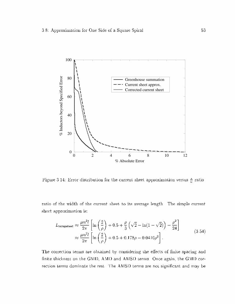
3.8: Approximation for One Side of a Square Spiral 53
0 2 4 6 8 10 12% Absolute Error
0
20
40
60
80
100%
Ind
ucto
rs b
eyon
d Sp
ecif
ied
Err
or Greenhouse summationCurrent sheet approx.Corrected current sheet
Figure 3.14: Error distribution for the current sheet approximation versus s
w
ratio.
ratio of the width of the current sheet to its average length. The simple current
sheet approximation is:
Lntrapsheet ��n2l
2�
�ln
�2
�
�+ 0:5 +
�
3
�p2� ln(1 +
p2)�+�2
24
�
��n2l
2�
�ln
�2
�
�+ 0:5 + 0:178�+ 0:0416�2
�:
(3.54)
The correction terms are obtained by considering the e�ects of �nite spacing and
�nite thickness on the GMD, AMD and AMSD terms. Once again, the GMD cor-
rection terms dominate the rest. The AMSD terms are not signi�cant and may be

54 Chapter 3: The Current Sheet Approach to Calculating Inductances
...
l l
II
I
I
ww wws s
d d
nI
�l = nw + (n� 1)s
t
Top View
Cross Section
1
2
(n� 1)n
Figure 3.15: Rectangular conductors with trapezoidal variation in length and the
equivalent current sheet representation

3.9: Approximation for a Square Spiral 55
ignored. Among the AMD correction terms, only the one for �nite spacing needs to
be included. The complete expression including the signi�cant correction terms is:
Lntrap;cor =�n2l
2�
�ln
�2
�
�+ 0:5 +
�
3
�p2� ln(1 +
p2)�+�2
24
�
+�n2l
2�
�0:5
(n� 1)s2
(�l)2+(n� 1)s
3nl
�p2� ln(1 +
p2)��
1
nln
�w + t
w
��
Lntrap;cor =�n2l
2�
�ln
�2
�
�+ 0:5 + 0:178�+ 0:0416�2
�
+�n2l
2�
�0:5
(n� 1)s2
(�l)2+ 0:178
(n� 1)s
n�
1
nln
�w + t
w
��:
(3.55)
The corrected and original current sheet expressions are compared with the more
exact summation method over a design space identical to the one described in sub-
section 3.7.1. Thus, we perform � 27; 000 simulations in which the s=w ratio varies
from 0 � 3. The results are summarized in Table 3.3 and Table 3.4 for maximum
s=w ratios of 1 and 3 respectively. Once again, we have included the inductance
calculated using the Greenhouse method for comparison. While the simple current
sheet expression exhibits errors within 4% for s=w ratios less than one, its worst case
error approaches �15% for s=w values close to 3. However, the corrected current
sheet expression exhibits errors within 3% over this entire range. It is interesting
to note that the Greenhouse method also exhibits errors as large as 7%. Such a
large error is the result of the Greenhouse method not accounting for the tapered
nature of trapezoidally shaped conductors. Consequently, a large discrepancy occurs
while computing the self inductance of such conductors when their width becomes
comparable to the length. In fact, the corrected current sheet expression's error
exhibits a smaller standard deviation than that of the inductance computed using
the Greenhouse method. These observations are con�rmed by Figure 3.16.
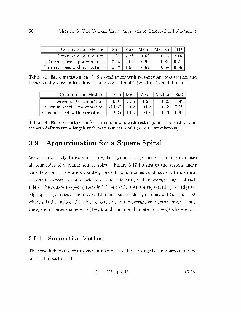
56 Chapter 3: The Current Sheet Approach to Calculating Inductances
Computation Method Min Max Mean Median StD
Greenhouse summation 0.01 7.38 1.63 0.45 2.16
Current sheet approximation -3.65 4.00 0.92 0.88 0.71
Current sheet with corrections -0.03 1.95 0.67 0.68 0.66
Table 3.3: Error statistics (in %) for conductors with rectangular cross section and
trapezoidally varying length with max s/w ratio of 1 (� 20; 000 simulations)
Computation Method Min Max Mean Median StD
Greenhouse summation 0.01 7.38 1.24 0.23 1.95
Current sheet approximation -14.30 4.02 0.09 0.69 2.19
Current sheet with corrections -2.25 1.95 0.68 0.70 0.67
Table 3.4: Error statistics (in %) for conductors with rectangular cross section andtrapezoidally varying length with max s/w ratio of 3 (� 2700 simulations)
3.9 Approximation for a Square Spiral
We are now ready to examine a regular, symmetric geometry that approximates
all four sides of a planar square spiral. Figure 3.17 illustrates the system under
consideration. There are n parallel, concentric, four-sided conductors with identical
rectangular cross section of width, w, and thickness, t. The average length of each
side of the square shaped system is l. The conductors are separated by an edge-to-
edge spacing s so that the total width of one side of the system is nw+(n�1)s = �l,
where � is the ratio of the width of one side to the average conductor length. Thus,
the system's outer diameter is (1+�)l and the inner diameter is (1��)l where � < 1.
3.9.1 Summation Method
The total inductance of this system may be calculated using the summation method
outlined in section 3.6,
LT= �L
i+ �M; (3.56)

3.9: Approximation for a Square Spiral 57
0 2 4 6 8 10 12% Absolute Error
0
20
40
60
80
100
% I
nduc
tors
bey
ond
Spec
ifie
d E
rror Greenhouse summation
Current sheet approx.Corrected current sheet
Figure 3.16: Comparison of error distribution of inductances evaluated for parallelinductors with trapezoidally varying length
where �Lidenotes the sum of self inductances of the segments and �M denotes
the sum of all the mutual inductances. Each conductor contains 4 straight line
segments. Thus our square system of n conductors has 4n segments, 2n of which are
orthogonal to the other 2n segments. Of the 2n parallel segments, n have current
ow in the opposite direction to the other n. Using symmetry and noting that
segments perpendicular to one another have zero mutual inductance, we may write
the total inductance as [15]:
LT = 4
nXi=1
Li+
nXi=1
nXj=1;j 6=i
M+;ij �nXi=1
2nXj=n+1
M�;ij
!(3.57)

58 Chapter 3: The Current Sheet Approach to Calculating Inductances
I
I
I
I
wwwwwwww ssss
dddd
t
Top view
Cross section
1
2
(n� 1)
n
Figure 3.17: System of parallel, concentric, square conductors

3.9: Approximation for a Square Spiral 59
l
II
I
I
wwwwwwww ssss
dddd
nI
�l = nw + (n� 1)s�l = nw + (n� 1)s
Top view
Cross section
1
2
(n� 1)n
Figure 3.18: Square geometry and equivalent current sheet
where Lidenotes the self inductance terms, M+;ij denotes the positive mutual in-
ductance terms and M�;ij denotes the negative mutual inductance terms. The self
and mutual inductances may be calculated using the expressions that we derived
in section 3.5, or by using the Greenhouse equations [15]. However, the complexity
of the system has order n2, making such an approach unacceptable for obtaining a
simple, accurate inductance expression. Thus, we will pursue an approach similar to
that outlined in sections 3.7 and 3.8 and explore how a current sheet approximation
combined with the dominant correction terms can render an expression that exhibits
very good accuracy.

60 Chapter 3: The Current Sheet Approach to Calculating Inductances
3.9.2 Current Sheet Approximation of Concentric, Parallel
Conductors with Four Sides
Once again we introduce the variable � =nw+(n�1)s
l
, which is now the ratio of the
width of the current sheet to the average length of one side of the current sheet.
The simple current sheet approximation is obtained from equation 3.34:
Lnsqsheet =2�n2l
�
�ln
�2:067
�
�+ 0:178�+ 0:125�2
�: (3.58)
The correction terms are obtained by considering the e�ect on �nite spacing and
�nite thickness on the GMD, AMD and AMSD terms. Once again, the GMD cor-
rection terms dominate. Among the AMD correction terms, only the one associated
with �nite spacing is signi�cant. The AMSD terms associated with the positive
mutual inductance terms may be ignored, although the correction terms involving
the negative mutual inductance terms must be included. The complete expression
including the signi�cant correction terms is:
Lnsq;cor =2�n2l
�
�ln
�2:067
�
�+ 0:178�+ 0:125�2 + 0:5
(n� 1)s2
(�l)2
�
+2�n2l
�
�0:178
(n� 1)s
nl+ 0:0833
(n� 1)s(s+ w)
l2�
1
nln
�w + t
w
��:
(3.59)
The corrected and original current sheet expressions are compared with the more ex-
act summation method over a design space identical to the one used in the previous
sections. The results are summarized in Table 3.5 and Table 3.6 for maximum s=w
ratios of 1 and 3 respectively. Once again, we have included the inductance calcu-
lated using the Greenhouse method for comparison. While the simple current sheet
expression exhibits errors as large as �7% for s=w ratios less than 1, the corrected
current sheet expression exhibits errors only within 3% for s=w ratios up to 3. Note
that the corrected current sheet expression's error exhibits a smaller standard devia-
tion (but a somewhat larger mean error) than that computed using the Greenhouse

3.10: Circular Geometries 61
method. Figure 3.19 compares the absolute error of the three expressions. Table 3.5
Table 3.6 Figure 3.19
Computation Method Min Max Mean Median StD
Greenhouse summation -1.81 2.76 0.76 0.17 1.06
Current sheet approximation -7.59 4.63 0.95 0.99 1.10
Current sheet with corrections -0.04 2.50 0.81 0.78 0.81
Table 3.5: Error statistics (in %) for conductors with rectangular cross section mak-
ing a square inductor with max s/w ratio of 1 (� 20; 000 simulations)
Computation Method Min Max Mean Median StD
Greenhouse summation -1.81 2.76 0.58 0.11 0.95Current sheet approximation -22.36 4.65 -0.29 0.74 3.32
Current sheet with corrections -3.44 2.50 0.80 0.82 0.85
Table 3.6: Error statistics (in %) for conductors with rectangular cross section mak-ing a square inductor with max s/w ratio of 3 (� 27; 000 simulations)
3.10 Circular Geometries
In this section, we will look at the self and mutual inductances of some circular ge-
ometries. Although not often used in practice, the results of circular geometries are
useful for bounding the inductances of polygonal spirals possessing a large number
of sides. Such bounds are of particular interest for on-chip spiral inductors, where
hexagonal, octagonal and other polygonal spirals are candidates for replacing square
spirals. In the previous sections, we have provided a comprehensive treatment of
straight, trapezoidal and square geometries. Now, we will provide a similar treat-
ment for circular geometries. We will see that these two extremes yield inductance
expressions that are similar in form. In many cases, the terms have the same avor
and retain the same order of importance.
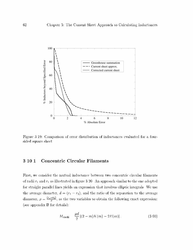
62 Chapter 3: The Current Sheet Approach to Calculating Inductances
0 2 4 6 8 10 12% Absolute Error
0
20
40
60
80
100%
Ind
ucto
rs b
eyon
d Sp
ecif
ied
Err
or Greenhouse summationCurrent sheet approx.Corrected current sheet
Figure 3.19: Comparison of error distribution of inductances evaluated for a four-sided square sheet
3.10.1 Concentric Circular Filaments
First, we consider the mutual inductance between two concentric circular �laments
of radii r1 and r1 as illustrated in �gure 3.20. An approach similar to the one adopted
for straight parallel lines yields an expression that involves elliptic integrals. We use
the average diameter, d = (r1 + r2), and the ratio of the separation to the average
diameter, � = (r1�r2)
d
, as the two variables to obtain the following exact expression:
(see appendix B for details):
Mcirc�l =�d
2[(2�m)K(m)� 2E(m)] : (3.60)

3.10: Circular Geometries 63
r1
r2
r = 0:5d = 0:5(r1 + r2)
�d = (r1 � r2)
Figure 3.20: Mutual inductance between concentric planar circular �laments
In this equation, K(m) is the complete elliptic integral of the �rst kind and E(m)
is the complete elliptic integral of the second kind, with argument m = (1 � �2).
A simpler expression may be obtained via series expansion in terms of �. This
approach yields an expression that resembles the approximate expression obtained
for the mutual inductance between two straight, parallel lines:
Mcirc�l ��d
2
�ln
�1
�
�� 0:6 + 0:7�2
�: (3.61)
This expression is accurate to within 5% for � < 0:6 and is good enough for most
practical cases.
3.10.2 Self Inductance of a Circular Sheet
Figure 3.21 shows a circular current sheet of average diameter, d, and width, w. The
self inductance of this sheet may be obtained by using equation 3.61 and then taking
the mean value of the terms. Once again, the GMD and AMSD concepts are used

64 Chapter 3: The Current Sheet Approach to Calculating Inductances
dw
Figure 3.21: Circular current sheet
(note that the AMD is not needed because the series expansion does not contain a
term linear in �). The result is (see appendix B for details): :
Lcircsheet ��d
2
�ln
�d
w
�+ 0:9 + 0:2
w2
d2
�: (3.62)
3.10.3 Mutual Inductance between Two Concentric Circular
Current Sheets
Figure B.3 shows two circular concentric current sheets of average diameters d1 and
d2. The sheets have equal width, w, and are separated by a center to center distance,
�d, where d is the mean of the two average diameters (d = 0:5(d1 + d2)). Note that
�d = w+ s. The mutual inductance between the sheets is given by (see appendix B
for details):
Mcirc2sheets =�d
2
�(2�m)K(m)� 2E(m) +
�0:2 +
1
12�2
�w2
d2
�; (3.63)

3.10: Circular Geometries 65
I
I
d1
d2�d = 0:5�(d1 + d2) = w + s
ww s
Figure 3.22: Mutual inductance between circular �laments
where the argument for the complete elliptic integrals is again given by m = (1��2).
An approximate series expansion of this expression, using techniques similar to the
ones used in straight and square geometries, yields:
Mcirc2sheets ��d
2
�ln
�1
�
�� 0:6 + 0:7�2 +
�0:2 +
1
12�2
�w2
d2
�: (3.64)
3.10.4 Parallel Concentric Circular Conductors
Figure 3.23 shows n circular concentric conductors each of width, w, and thickness,
t. The edge-to-edge spacing is s. The equivalent current sheet approximation is also
shown in the �gure. This equivalent current sheet has the same average diameter, d,
as the system of n conductors. The width of the current sheet is �d = nw+(n�1)s.
The current sheet expression for the system is simply the self inductance of the
equivalent current sheet:
Lncircsheet ��n2d
2
�ln
�d
w
�+ 0:9 + 0:2
w2
d2
�: (3.65)

66 Chapter 3: The Current Sheet Approach to Calculating Inductances
...
I
I
I
www
s
ddnI
�d = nw + (n� 1)s1 2 n
Figure 3.23: Concentric circular conductors with rectangular cross sections
A more accurate expression may be obtained by considering the �nite spacing be-
tween the conductors as well as the thickness of the conductors. Just as in the case of
the straight, parallel conductors, the dominant correction terms are the GMD ones.
No AMD correction term is needed as there is no AMD term in the approximate
expression. Among the AMSD correction terms, only the one for �nite spacing is
signi�cant. The corrected expression is:
Lncirc;cor ��n2d
2
�ln
�d
w
�+ 0:9 + 0:2
w2
d2
�
+�n2d
2
�0:5(n� 1)s2
(�d)2+0:4(n� 1)s(w + s)
d2�
1
nln
�w + t
w
�� (3.66)
Table 3.7 and Table 3.8 summarize the accuracy of these expressions for s=w ratios up
to 1 and 3 respectively. While the simple current sheet approximation is good enough
for s=w ratios up to 1, the corrected current sheet expression is more appropriate for
a larger design space. The corrected expression exhibits errors within 3% for s=w
ratios up to 3. Figure 3.24 compares the absolute errors of the two expressions.

3.11: Summary 67
Computation Method Min Max Mean Median StD
Current sheet approximation -7.94 3.78 0.08 0.37 1.28
Current sheet with corrections -3.35 2.00 -0.06 - 0.00 0.75
Table 3.7: Error statistics (in %) for circular concentric conductors with rectangular
cross section with max s/w ratio of 1 (� 20; 000 simulations)
Computation Method Min Max Mean Median StD
Current sheet approximation -21.90 3.94 -0.92 0.11 3.04Current sheet with corrections -3.35 2.08 0.13 -0.00 0.82
Table 3.8: Error statistics (in %) for circular concentric conductors with rectangular
cross section with max s/w ratio of 3 (27; 000 simulations)
3.11 Summary
In this chapter, we have shown how a current sheet based approach can provide
simple, accurate expressions for the self and mutual inductances of a variety of
geometries. These approximate expressions have been compared to those obtained
from more exact (but more complicated) summation methods. The errors of the
approximate expressions are within � 4% for s=w ratios less than 1. We have
shown how the inclusion of some correction terms can enhance the accuracy of
these expressions over a wide design space, yielding errors within � 4% of the more
accurate summation method for s=w ratios as large as 3.
As emphasized in chapter 2, the expressions that we derived here are intended for
exploring trade-o�s, obtaining design insight and optimizing circuits with on-chip
inductors. In chapter 4, we will see how the approach developed in this chapter can
be easily extended to obtain simple accurate expressions for square, hexagonal and
octagonal spiral inductors.

68 Chapter 3: The Current Sheet Approach to Calculating Inductances
0 2 4 6 8 10 12% Absolute Error
0
20
40
60
80
100
% I
nduc
tors
bey
ond
Spec
ifie
d E
rror Current sheet approx.
Corrected current sheet
Figure 3.24: Comparison of error distribution of expressions for the total inductanceof concentric circular conductors with rectangular cross sections

Chapter 4
Simple Accurate Expressions for
the Inductance of Planar Spirals
IN this chapter, we describe three new simple expressions for the inductance of
square, hexagonal, octagonal and circular planar inductors. The �rst expression
is obtained from the current sheet approach described in chapter 3; the second is a
monomial expression derived from �tting to a large database of inductors generated
by a �eld solver; and the third is based on a modi�cation of an expression developed
by Wheeler [26]. These expressions are presented in section 4.1. The accuracy of
these new expressions (as well as the previously published expressions reported in
chapter 2) are compared to �eld solver simulations over a wide design space (spanning
more than 19; 000 inductors) in section 4.2 and then compared to measurement
results in section 4.3. All three expressions are accurate, with typical errors of 2{
3%, about an order of magnitude better than the previously published expressions,
which have typical errors around 20% (or more). Furthermore, these new expressions
are simple and are therefore excellent candidates for use in design and optimization.
4.1 Simple, Accurate Expressions
This section presents several accurate expressions for the inductance of square,
hexagonal, octagonal and circular spirals.
69

70 Chapter 4: Simple Accurate Expressions for the Inductance of Planar Spirals
s
wdout
nI
davg
�davg
4.1.1 Expressions Based on Current Sheet Approximations
Simple and accurate expressions for the inductance of a planar spirals can be ob-
tained by approximating the sides of the spirals by symmetrical current sheets of
equivalent current densities. For example, as illustrated in �gure 4.1.1, in the case
of the square, we obtain four identical current sheets: the current sheets on opposite
sides are parallel to one another, whereas the adjacent ones are orthogonal. Using
symmetry and the fact that sheets with orthogonal current sheets have zero mutual
inductance, the computation of the inductance is now reduced to evaluating the self
inductance of one sheet and the mutual inductance between opposite current sheets.
These self and mutual inductances are evaluated using the concepts of GMD, AMD
and AMSD. The resulting expression is:
Lcursh =�n2davgc1
2
�ln(c2=�) + c3� + c4�
2�; (4.1)
where the coe�cients ciare layout dependent and are shown in Table 4.1. The
derivations of the expressions for a square and circular spiral were discussed in detail
in the previous chapter. The expressions for the hexagonal and octagonal spirals
(and for that matter a polygonal spiral with an arbitrary number of sides) are also
obtained using the same concepts, but require more work. In general, an N sided

4.1: Simple, Accurate Expressions 71
Layout c1 c2 c3 c4
Square 1.27 2.07 0.18 0.13
Hexagonal 1.09 2.23 0.00 0.17
Octagonal 1.07 2.29 0.00 0.19
Circle 1.00 2.46 0.00 0.20
Table 4.1: Coe�cients for current sheet expression.
polygonal spiral can be approximated by an N sided regular polygonal current sheet.
The calculation of the inductance of this regular polygonal current sheet involves
the calculation of N
2distinct terms. Thus, as N becomes large, the computation
of the coe�cients cibecomes increasingly tedious, albeit signi�cantly less complex
than calculating the inductance of a spiral using a segmented summation method
(such as the one proposed by Greenhouse).
For su�ciently large values N , the polygonal current sheet is well approximated
by a circular sheet, signi�cantly simplifying the inductance calculation. For practical
spiral geometries, the circular sheet approximation is within 3% of the polygonal
current sheet approximation for N > 12. In fact, most of the coe�cients tabulated
in 4.1 can be well approximated by those obtained from corrections to an equivalent
circular current sheet. For example, c1 is roughly the ratio of the area of a polygon
to that of a circle for a �xed diameter so that:
c1 �N
�tan� �N
�: (4.2)
It can be easily veri�ed that c1 approaches unity as N becomes large. Similarly, the
GMD and ASMD coe�cients c2 and c4 also exhibit monotonic transitions from the
square to the circular current sheet. One would expect a similar transition for the
AMD coe�cent c3. However, the magnitude of c3 decays rapidly as a function of
N and is signi�cant only for the square case. The reason for this rapid decay can
be attributed to the fact that the AMD term only appears in the self inductance
calculation of one side of a spiral: as N increases (while keeping the average diameter
davg �xed), not only does the length of a side decrease, but also the relative weight
of self inductance terms goes down as 1N
.

72 Chapter 4: Simple Accurate Expressions for the Inductance of Planar Spirals
4.1.2 Data Fitted Monomial Expression
Our second expression is based on a data �tting technique, and has the form:
Lmon = �d�1outw�2d�3avgn
�4s�5 ; (4.3)
where the coe�cients � and �iare layout dependent, and given in Table 4.2. The
Layout � �1 (dout) �2 (w) �3 (davg) �4 (n) �5 (s)
Square 1:62 � 10�3 -1.21 -0.147 2.40 1.78 -0.030
Hexagonal 1:28 � 10�3 -1.24 -0.174 2.47 1.77 -0.049Octagonal 1:33 � 10�3 -1.21 -0.163 2.43 1.75 -0.049
Table 4.2: Coe�cients for data-�tted monomial expression.
expression in (4.3) is called a monomial in the variables dout, w, davg, n, and s. The
coe�cients are obtained as follows. We �rst change variables to use the logarithms
of the variables:
x1 = log dout; x2 = logw; x3 = log davg; x4 = logn; x5 = log s:
Taking the logarithm of the inductance as well we can express the monomial rela-
tion (4.3) as
y = logL = �0 + �1x1 + �2x2 + �3x3 + �4x4 + �5x5
where �0 = log�. This is a linear-plus-constant model of y as as function of x, and
is easily �t by various regression or data-�tting techniques. To develop our models
we use a simple least-squares �t: we chose �ito minimize
NXk=1
�y(k) � �0 � �1x
(k)1 � �2x
(k)2 � �3x
(k)3 � �4x
(k)4 � �5x
(k)5
�2;

4.1: Simple, Accurate Expressions 73
where the sum is over our family of inductors (so N � 19; 000). It is also possible to
use more sophisticated data-�tting techniques, e.g., one which minimizes the maxi-
mum error of the �t, or one in which the coe�cients must satisfy given inequalities
or bounds.
For all three cases tabulated in table 4.2, the exponents of the variables with the
dimension of length (dout, w, davg and s) sum to unity, which is consistent with the
expectation that the inductance scales linearly with the size of a spiral.
Since the monomial expression Lmon is developed from our library of inductors,
it is important to check that it has predictive ability as well, by checking its error
on inductors not in the library. Such tests reveal that the �t for such inductors is
as good as the �t for the ones in the family from which the model was developed.
This is hardly surprising since the �tting method compresses 19; 000 numbers (i.e.,
the inductances) to 6 (i.e., the monomial coe�cients), and so is not prone to `over-
�tting'.
The monomial expression is useful since, like the other expressions, it is very
accurate and very simple. Its real use, however, is that it can be used for optimal
design of inductors and circuits containing inductors, using geometric programming,
which is a type of optimization method that uses monomial models [27, 28, 29].
4.1.3 Modi�ed Wheeler formula
H. Wheeler [26] presented several formulas for planar spiral inductors, which were
intended for discrete inductors. We have found that a simple modi�cation of the
original Wheeler formula allows us to obtain an expression that is valid for planar
spiral integrated inductors:
Lmw = K1�0n2davg
1 +K2�(4.4)
where � is the �ll ratio de�ned previously. The coe�cients K1 and K2 are layout
dependent and are shown in Table 4.3. The ratio � represents how hollow the
inductor is: for small � we have a hollow inductor (dout � din) and for a large � we

74 Chapter 4: Simple Accurate Expressions for the Inductance of Planar Spirals
Layout K1 K2
Square 2.34 2.75
Hexagonal 2.33 3.82
Octagonal 2.25 3.55
Table 4.3: Coe�cients for modi�ed Wheeler expression.
have a full inductor (dout � din). Two inductors with the same average diameter but
di�erent �ll ratios will, of course, have di�erent inductance values: The full one has
a smaller inductance because its inner turns are closer to the center of the spiral, and
so contribute less positive mutual inductance and more negative mutual inductance.
4.2 Comparison to �eld solvers
In this section we analyze the error distributions of previously published expressions
as well as our expressions by comparing them to the inductance computed using the
�eld solver ASITIC.
Figure 4.1 shows the absolute error distributions of previously published expres-
sions for square inductors presented in chapter 2. Figure 4.2 shows the absolute error
distributions of our expressions for the same set of square inductors. The compari-
son is carried out for � 19; 000 inductors spanning a wide design space. Table 4.4
summarizes the extent of the design space.
While the previously published expressions do predict the correct order of mag-
nitude of the inductance, typical errors are 20% or more, which is unacceptable for
circuit design and optimization. On the other hand all of the new expressions exhibit
substantially better accuracies, with typical errors of � 2� 3%.
Table 4.5 summarizes the error statistics of our expressions for this design space.
The current sheet expression exhibits the best performance with worst case errors
less than 9%. The monomial expression exhibits a worst case error of 12% whereas
the modi�ed Wheeler expression has errors as large as 22% for a few inductors. The
mean errors of all the expressions are less than 1% and the standard deviations are
� 2�3% indicating that all three expressions give good accuracy for most inductors.

4.2: Comparison to �eld solvers 75
00
20
20
40
40
60
60
80
80
100
Crols [8]
Voor [17]
Bryan [19]
Ron [20]
Dill [18]
% Absolute Error
%
InductorsbeyondSpeci�edError
Figure 4.1: Error distribution for previously published expressions for square induc-
tors, compared to �eld solver simulations.
Min Max
L(nH) 0:1 71OD(�m) 100 400
n 1 20
s=w 0:02 3� 0:03 0:95
Table 4.4: Design space used for simulating square inductors

76 Chapter 4: Simple Accurate Expressions for the Inductance of Planar Spirals
Current SheetMonomial FitModified Wheeler
2 4 6 8 10 1200
20
40
60
80
100
% Absolute Error
%
InductorsbeyondSpeci�edError
Figure 4.2: Error distribution for the new expressions for square inductors, compared
to �eld solver simulations (Note change of x-axis scale relative to �gure 4.1).
Computation Method Min Max Mean Median StD
Current sheet -8.75 5.84 -0.85 -0.47 2.35
Monomial �t -12.46 14.34 -0.16 -0.01 3.04
Modi�ed wheeler -22.90 7.21 -0.33 0.14 3.25
Table 4.5: Error statistics (in %) of expressions for square inductors (� 19; 000
simulations)

4.2: Comparison to �eld solvers 77
Current SheetMonomial FitModified Wheeler
2 4 6 8 10 1200
20
40
60
80
100
% Absolute Error
%
InductorsbeyondSpeci�edError
Figure 4.3: Error distribution for the new expressions for hexagonal inductors, com-
pared to �eld solver simulations (� 8; 000).
Figure 4.3 shows the absolute error distributions of our expressions for hexag-
onal inductors. The comparison is carried out for � 8; 000 inductors spanning a
wide design space. Table 4.6 summarizes the extent of the design space. Table 4.7
summarizes the error statistics of our expressions for this design space. Once again,
the current sheet expression exhibits the best performance with worst case errors
less than 9%.
Figure 4.4 shows the absolute error distributions of our expressions for octag-
onal inductors. The comparison is carried out for � 12; 000 inductors spanning a
wide design space. Table 4.8 summarizes the extent of the design space. Table 4.9

78 Chapter 4: Simple Accurate Expressions for the Inductance of Planar Spirals
Min Max
L(nH) 0:1 48
OD(�m) 90 350
n 1 20
s=w 0:03 3� 0:01 0:90
Table 4.6: Design space used for simulating hexagonal inductors
Computation Method Min Max Mean Median StD
Current sheet -9.62 7.25 -0.28 -0.26 2.88Monomial �t -11.38 12.08 0.24 0.71 3.68Modi�ed wheeler -29.84 8.11 -0.39 0.44 4.43
Table 4.7: Error statistics (in %) of expressions for hexagonal inductors (� 8; 000
simulations)
summarizes the error statistics of our expressions for this design space. The current
sheet expression exhibits the best performance with worst case errors less than 9%.
4.3 Measurement Results
In this section, we compare the inductance values predicted by previously published
expressions as well as new expressions to measurement results. We use both our own
measurements as well as previously published measurements.
Figure 4.5 shows the measurement setup. The raw S parameters of the device
under test (DUT) are used to extract the low frequency inductance, L, as follows:
Min Max
L(nH) 0:1 57
OD(�m) 100 360
n 1 20
s=w 0:03 3� 0:01 0:90
Table 4.8: Design space used for simulating octagonal inductors

4.3: Measurement Results 79
Current SheetMonomial FitModified Wheeler
2 4 6 8 10 1200
20
40
60
80
100
% Absolute Error
%
InductorsbeyondSpeci�edError
Figure 4.4: Error distribution for the new expressions for octagonal inductors, com-
pared to �eld solver simulations (� 12; 000).
Computation Method Min Max Mean Median StD
Current sheet -9.77 4.98 -0.72 -0.09 2.78
Monomial �t -12.88 10.18 -0.00 0.60 3.51
Modi�ed wheeler -28.59 6.84 -0.28 0.76 3.87
Table 4.9: Error statistics (in %) of expressions for octagonal inductors (� 12; 000
simulations)

80 Chapter 4: Simple Accurate Expressions for the Inductance of Planar Spirals
S parameters
DUT
Coplanar GSG probes
HP8720B
network analyzer
50 environment
port 1 port 2
Figure 4.5: Experimental set up for measuring inductance
port 1 port 2
Y11 � Y12Y22 � Y12
Y12
Figure 4.6: Y parameter extraction

4.3: Measurement Results 81
1. DUT : S-to-Y (YDUT)
2. Open calibration: S-to-Y (YO)
3. YCor = YDUT � YO
4. YCor to equivalent � model as illustrated in �gure 4.6
5. L = 1!
IMAG( 1Y12
)
Figure 4.7 compares the experimental values to the inductances predicted by
previously published expressions, while Figure 4.8 compares the experimental values
to the inductance predicted by our formulas as well as ASITIC. Once again, it is
clear that our expressions exhibit much smaller errors compared to the previous
ones. It is also interesting to note how well the predictions of ASITIC compare to
our expressions. This is particularly of interest in those few cases where the errors
between experiment and our expressions approach 20%, which suggests substantial
measurement errors, either in calibration or parameter extraction. More important,
it is clear that our expressions perform as well as a �eld solver.
In Table 4.10 we compare the measured inductance values with those predicted
by the various expressions. The �rst �fteen inductors shown in Table 4.10 were
fabricated using the top metal level (of thickness 0:9�m) of a 0:35�m CMOS process.
The data for the remaining inductors were obtained from previously published work.
The �rst column in Table 4.10 gives the inductor number; the second column shows
the source of the inductor data; the third column shows the number of sides; the
fourth is the number of turns (n); the �fth, sixth and seventh columns are the outer
diameter (dout)turn width (w) and spacing (s) in �m; the eighth column shows the
measured or reported value of the inductance (Lmeas) in nH. In the ninth column
we give the percent relative error between Lmeas and (Lasi predicted by ASITIC ),
which we de�ne as emeas = 100 (Lmeas � Lasi) =Lmeas. In the �nal three columns
we give the corresponding relative errors ewhe, egmd and emon for our inductance
expressions (4.4), (4.1) and (4.3) respectively.
We observe close agreement between our expressions and the measured data,
with larger errors for the smaller inductors. The reason, as explained in [5], is that

82 Chapter 4: Simple Accurate Expressions for the Inductance of Planar Spirals
00
20
20
40
40
60
60
80
80
100
Crols [8]
Voor [17]
Bryan [19]
Ron [20]
Dill [18]
% Absolute Error
%
InductorsbeyondSpeci�edError
Figure 4.7: Error distribution of previous formulas, compared to measurements.

4.3: Measurement Results 83
ASITICCurrent SheetModified WheelerMonomial Fit
4 8 12 1600
20
20
40
60
80
100
% Absolute Error
%
InductorsbeyondSpeci�edError
Figure 4.8: Error distribution of new expressions, compared to measurements.

84 Chapter 4: Simple Accurate Expressions for the Inductance of Planar Spirals
the parasitic inductance inherent in the measurement setup results in large apparent
relative errors for low inductance values.
We can also put the accuracy of our formulas in the context of other variations
and uncertainties in a spiral inductor. A major limitation in the design, modeling
and simulation of spirals is the uncertainty in the oxide thickness due to process
variations. Process variations can cause the parasitic capacitances in the inductor
model to vary by around 5{10%. These variations translate to an uncertainty in
the impedance of the spiral that is of the same order of magnitude as the errors
introduced by our expressions. This limitation suggests that inductance expressions
with better accuracies than what we have achieved are not necessary and that our
expressions are acceptable for use in circuit design and optimization.
4.4 Summary
In this chapter, we have presented three simple, approximate expressions for spiral
inductors of square, hexagonal and octagonal geometries. The �rst expression is
derived from electromagnetic principles by approximating the sides of the spiral by
current sheets with uniform current distribution. This expression is intuitive and
similar in form to inductance expressions for more conventional elements such as
coaxial transmission lines and parallel wire transmission lines. The second expression
is obtained by data-�tting the coe�cients with a monomial expression. Although it
lacks the physically intuitive derivation of the �rst expression, it is very well suited
for optimization of circuits using geometric programming. The �nal expression,
called the modi�ed Wheeler expression, is obtained by modifying an expression that
Wheeler obtained for discrete inductors.
All three expressions match �eld solver simulations well, with typical errors of 2{
3%, and most errors smaller than around 8%. This represents a great improvement
over previously published expressions, which have typical errors of around 20% or
more. When compared to experimental data, the errors of our three expressions are
comparable to those of a �eld solver, which suggests that the errors may be due, at
least in part, to measurement error. The simplicity, versatility and robustness of our

4.4: Summary 85
Inductor # Source sides n dout w s Lmeas easi ewhe egmd emon
1 1 4 2.75 344 29.7 1.9 3.20 3.1 5.2 6.4 3.6
2 1 4 3.75 292 13.0 1.9 6.00 -1.7 -1.2 -0.7 -0.4
3 1 4 6.50 217 5.4 1.9 12.50 2.4 1.4 2.3 4.9
4 1 4 2.75 279 18.3 1.9 3.10 0.0 2.1 2.8 1.4
5 1 4 4.75 206 7.8 1.9 6.10 0.0 -0.7 0.3 2.0
6 1 4 7.50 166 3.2 1.9 12.40 4.0 2.2 3.2 5.5
7 1 4 9.50 153 1.8 1.9 18.20 2.7 0.8 1.9 2.7
8 1 4 2.75 277 18.3 0.8 3.10 0.0 0.8 1.3 -2.0
9 1 4 2.75 307 18.3 18.0 2.90 10.3 13.5 14.6 12.4
10 1 4 3.75 321 16.5 1.9 6.10 0.0 0.2 1.1 0.7
11 1 4 7.75 225 4.4 1.9 18.10 0.6 -0.9 0.0 2.9
12 1 4 3.75 193 9.1 1.9 4.00 7.5 6.6 7.5 8.4
13 1 4 5.00 171 5.4 1.9 6.10 4.9 3.0 3.8 5.8
14 1 4 3.25 400 31.6 1.9 4.90 4.1 7.2 8.3 5.9
15 1 4 5.75 339 10.0 1.9 16.20 3.7 2.0 2.7 4.5
16 1 4 12.00 180 3.2 2.1 20.50 2.0 -1.0 -0.4 3.9
17 1 4 7.00 300 13.0 7.0 8.00 5.0 5.6 4.0 9.1
18 [7] 4 6.00 400 24.0 7.0 8.00 8.8 9.2 7.6 12.6
19 [7] 4 8.00 300 5.0 4.0 22.10 -6.3 -9.6 -8.3 -7.6
20 [7] 4 4.00 300 5.0 4.0 9.20 -5.4 -3.3 -7.2 -6.4
21 [9] 4 9.00 210 6.5 5.5 7.70 2.6 8.0 4.5 11.8
22 [9] 4 8.00 226 6.0 6.0 9.00 -1.1 -1.0 -1.4 0.7
23 [16] 4 11.00 300 9.0 4.0 15.50 -11.6 -9.7 -12.4 -3.2
24 [16] 4 8.00 300 14.0 4.0 8.30 -8.4 -6.7 -9.5 -0.9
25 [16] 4 6.00 300 19.0 4.0 5.10 -7.8 -7.2 -9.1 -2.8
26 [16] 4 3.00 300 19.0 4.0 3.30 -6.1 -7.2 -6.1 -6.5
27 [16] 4 5.00 300 24.0 4.0 3.50 -5.7 -5.2 -7.3 -1.6
28 [16] 4 9.00 230 6.5 5.5 9.70 1.0 2.3 0.6 5.6
29 [16] 4 16.00 300 5.0 4.0 34.00 -7.6 -4.2 -6.9 1.6
30 [16] 4 6.00 300 9.0 4.0 11.70 -5.1 -7.8 -6.5 -4.9
31 [16] 4 3.00 300 9.0 4.0 5.50 5.5 6.3 3.7 4.8
32 [16] 4 4.00 300 14.0 4.0 5.80 -1.7 -4.4 -3.2 -2.6
33 [16] 4 2.00 300 14.0 4.0 2.90 17.2 18.0 15.0 15.5
34 [16] 4 2.00 300 19.0 4.0 2.50 16.0 16.0 15.0 14.5
35 [16] 4 3.00 300 24.0 4.0 3.10 9.7 5.9 7.1 6.5
36 [30] 4 5.00 154 7.0 5.0 3.00 6.7 3.9 4.3 5.8
37 [30] 4 9.00 250 7.0 5.0 12.00 -0.8 0.2 -0.5 3.7
38 [6] 4 6.00 285 15.0 3.0 6.70 -7.5 -9.4 -9.1 -5.6
39 [6] 4 3.50 255 10.0 1.5 5.00 -4.0 -4.5 -5.2 -4.4
40 [6] 4 4.50 216 10.0 1.5 5.00 -6.0 -7.8 -6.6 -5.4
41 [6] 4 5.50 199 10.0 1.5 5.00 -6.0 -9.3 -8.2 -5.8
42 [6] 4 6.50 191 10.0 1.5 5.00 -6.0 -8.1 -8.1 -3.6
43 [20] 4 7.50 190 10.0 1.5 5.00 -10.0 -8.5 -10.4 -2.8
44 [31] 4 9.25 145 5.2 2.0 6.00 -3.3 -5.2 -7.0 1.3
45 [31] 4 6.75 290 13.0 7.0 7.10 1.4 3.5 2.0 7.0
46 [31] 4 2.50 290 13.0 7.0 3.00 -3.3 -2.5 -3.3 -3.4
47 [32] 4 3.25 340 25.0 6.0 3.30 -9.1 -12.1 -10.8 -11.0
48 [32] 4 4.50 300 23.0 6.0 3.40 -2.9 -4.3 -5.1 -1.4
49 [32] 4 3.00 300 18.0 6.0 3.30 -3.0 -5.9 -4.7 -5.0
50 [32] 4 5.75 190 9.5 6.0 3.40 0.0 2.5 1.1 5.6
51 [32] 4 3.00 700 90.0 6.0 3.70 -5.4 -4.9 -5.4 -6.7
52 [33] 4 4.00 262 16.0 10.0 2.60 -19.2 -19.9 -19.5 -18.5
53 [33] 4 6.00 392 16.0 10.0 8.80 -11.4 -12.6 -12.4 -10.5
54 [33] 4 8.00 532 16.0 10.0 20.40 -16.7 -17.3 -17.1 -14.6
55 [?] 8 4.00 346 18.0 2.0 5.90 0.0 -1.1 -1.6 -3.6
56 [?] 8 5.00 346 18.0 2.0 7.50 2.7 2.7 0.7 0.3
57 [?] 8 4.00 326 8.0 12.0 5.60 -7.1 -7.7 -7.8 -11.8
58 [?] 8 5.00 326 8.0 12.0 7.20 -2.5 -1.0 -2.8 -5.6
59 [11] 12 6.75 197 8.2 3.0 5.45 1.8 - 1.5 -
60 [11] 12 8.00 198 7.5 3.0 6.30 -0.5 - -1.8 -
61 [11] 12 7.75 198 6.5 3.0 7.30 -1.9 - -2.2 -
Table 4.10: Comparison of measured inductance values with �eld solver inductance
values and the various approximate expressions.

86 Chapter 4: Simple Accurate Expressions for the Inductance of Planar Spirals
expressions make them good candidates for circuit design. They can be included in
a physical, scalable lumped-circuit model for spiral inductors where, in addition to
providing design insight, they allow e�cient optimization schemes to be employed.

Chapter 5
Modeling and Characterization of
On-Chip Transformers
This chapter discusses the modeling of on-chip transformers. Section 5.1 introduces
the main elements of an ideal transformer and then considers the parasitics present
in practical transformer realizations. Section 5.2 compares the advantages and dis-
advantages of various on-chip transformer realizations. Section 5.3 expands upon the
lumped inductor model presented in chapter 2 to model on-chip transformers. A key
element in these transformer models is the mutual inductance between the primary
and secondary. Sections 5.3.1 and 5.3.2 describe how the current sheet approach
developed in chapter 3 and inductance expressions developed in chapter 4 can be
used to obtain simple expressions for the mutual inductance and mutual coupling
coe�cient (k) of a variety of on-chip transformer realizations. Section 5.4 provides
expressions for the parasitic resistances and capacitances in the transformer models.
Section 5.5 illustrates, with examples, how the concepts developed in the preceding
sections may be applied to obtain on-chip transformer models. The predictions of
these models are compared to experimental results in section 5.6.
5.1 Transformer Fundamentals
An ideal transformer, as illustrated in �gure 5.1 contains three components:
87

88 Chapter 5: Modeling and Characterization of On-Chip Transformers
i1 i2
v1 v2
+ +
� �L1 L2
M
Figure 5.1: Ideal transformer
1. The self inductance of the primary (L1).
2. The self inductance of the secondary (L2).
3. The mutual inductance between the primary and the secondary (M).
The terminal voltages and currents of an ideal transformer are speci�ed by equa-
tion 5.1:
v1 = L1
@i1
@t+M
@i2
@t
v2 = L2
@i2
@t+M
@i1
@t:
(5.1)
The mutual inductance, M , is related to the self inductances, L1 and L2, by the
mutual coupling coe�cient, k:
k =M
pL1L2
: (5.2)
In general, jkj � 1 because the transformer is a passive device. While k = 1 for an
ideal transformer, most practical on-chip transformers exhibit k values between 0:3�
0:9. In addition to reduced k, practical transformers su�er from several nonidealities.
Figure 5.2 illustrates the important parasitic resistances and capacitances present
in practical transformers. Resistances R1 and R2 model the series resistances of
the primary and secondary spirals respectively. The �gure also shows the various

5.1: Transformer Fundamentals 89
L1 L2
M
R1 R2
Cs;11 Cs;22
Cs;12
Cs;21
Rsi;1aCsi;1a
Cox;1a
Rsi;1bCsi;1b
Cox;1b
Rsi;2aCsi;2a
Cox;2a
Rsi;2bCsi;2b
Cox;2b
subsub
subsub
primary secondary
Figure 5.2: Nonideal transformer

90 Chapter 5: Modeling and Characterization of On-Chip Transformers
elements used to model the spiral-to-substrate oxide capacitances (Cox;1a, Cox;1b,
Cox;2a and Cox;2b), the terminal-to-terminal oxide capacitances (Cs;11, Cs;22, Cs;12 and
Cs;21) and the resistive and capacitive coupling to the substrate (Rsi;1a, Csi;1a, Rsi;1b,
Csi;1b, Rsi;2a, Csi;2a, Rsi;2b and Csi;2b).
A transformer may be con�gured as a three or four terminal device. Further-
more, one or more terminals may be connected to incremental ground. The self
inductances, series resistances and mutual inductances are independent of the con-
�guration of the transformer. However, some of the capacitive elements may be
shorted out. This situation is analogous to that a spiral inductor being used as
either a single or dual terminal device.
5.2 Monolithic Transformer Realizations
The relative importance of the parasitic elements varies among di�erent transformer
realizations and con�gurations. This section discusses various on-chip transformer
realizations and highlights the dominant non-idealities.
5.2.1 Tapped Transformer
The tapped transformer, illustrated in �gure 5.3 is best suited for three-terminal
applications. Although not symmetric, it permits a variety of tapping ratios to be
realized. This transformer relies only on lateral magnetic coupling. All windings can
be implemented with the top metal layer, thereby minimizing terminal-to-substrate
capacitances. Since the two inductors occupy separate regions, the self-inductance is
maximized while the terminal-to-terminal capacitance is minimized. Unfortunately,
this spatial separation also leads to low mutual coupling (k � 0:3� 0:5).
5.2.2 Interleaved Transformer
The interleaved transformer, illustrated in �gure 5.4 is best suited for four-terminal
applications that demand symmetry. Once again, capacitances can be minimized by
implementation on top level metal so that high resonant frequencies may be realized.

5.2: Monolithic Transformer Realizations 91
Inner
spiral
Outer spiral
Figure 5.3: Tapped transformer
Primary Secondary
Figure 5.4: Interleaved transformer

92 Chapter 5: Modeling and Characterization of On-Chip Transformers
Top View
Side View
top spiral
bottom spiral
Figure 5.5: Stacked transformer
The interleaving of the two inductances permit moderate coupling (k � 0:7) to be
achieved at the cost of reduced self-inductance. This coupling may be increased at
the cost of higher series resistance by reducing the turn width, w, and spacing, s.
5.2.3 Stacked Transformer
The stacked transformer, illustrated in �gure 5.4 uses multiple metal layers and ex-
ploits both vertical and lateral magnetic coupling to provide the best area e�ciency,
the highest self-inductance and highest coupling (k � 0:9). This con�guration is
suitable for both three and four terminal con�gurations. The main drawback is

5.2: Monolithic Transformer Realizations 93
Bottom spiral Top spiral
xs
Figure 5.6: Stacked transformer with top and bottom spiral laterally shifted
the high terminal-to-terminal capacitance, or equivalently a low self-resonance fre-
quency. In some cases, such as narrowband transformers, this capacitance may be
incorporated as part of the resonant circuit. Also, in modern multilevel processes,
the capacitance can be reduced by increasing the oxide thickness between spirals.
For example, in a �ve metal process, 50 � 70% reductions in terminal-to-terminal
capacitance can be achieved by implementing the spirals on layers �ve and three
instead of �ve and four. The increased vertical separation reduces k by less than
5%.
5.2.4 Variations on the Stacked Transformer
As illustrated in �gures 5.6 and 5.7, one can trade o� reduced k for reduced terminal-
to-terminal capacitance by displacing the centers of the stacked inductors either
laterally or diagonally.

94 Chapter 5: Modeling and Characterization of On-Chip Transformers
ysds
xs
Figure 5.7: Stacked transformer with top and bottom spiral diagonally shifted
5.2.5 Stacked InterleavedTransformer
One potential drawback of the stacked transformer and its variations discussed so far
is that these realizations are not symmetric. A symmetric transformer that achieves
the area e�ciency of a stacked transformer may be obtained by stacking two inter-
leaved transformers on top of one another. Figure 5.8 illustrates the details of such a
stacked interleaved transformer. Unlike the stacked transformer where the primary
and secondary occupy distinct metal layers, the stacked interleaved transformer has
the primary and secondary spirals interleaved on both layers, thereby achieving a
symmetrical layout.
In this case, the primary spirals are stacked on top of one another (except of
course for the crossover points required to keep the same current orientation in the
top and bottom spirals) and so are the secondary spirals. This implementation
minimizes the primary-to-secondary capacitance at the cost of increased primary-
to-primary and secondary-to-secondary capacitance. In tuned circuit applications,
the primary-to-primary and secondary-to-secondary capacitances are more easily

5.2: Monolithic Transformer Realizations 95
Contact totop layerprimary
Contact totop layersecondary
��������
����
Bottom layer
Top view of
Cross section cut
terminalBottom secondary
Bottom primaryterminal
Bottom layer
Top layerCross-section
Top primaryterminal
����
����
Top layer
Top view of
Cross section cut
terminalTop secondaryContact to
primarybottom layer
Contact to
secondarybottom layer
A
B
B
A
Figure 5.8: Stacked interleaved transformer

96 Chapter 5: Modeling and Characterization of On-Chip Transformers
incorporated into the tuning network than the primary-to-secondary capacitance.
Therefore, this transformer is ideal for those narrowband applications that require
symmetry.
The mutual coupling coe�cient of the stacked interleaved transformer is com-
parable to that of the interleaved transformer. However, the stacking of multiple
layers enables an increase in the overall inductance density by a factor of � 3:5�3:9.
The self inductances of the primary and secondary are larger than the correspond-
ing stacked transformer implementation. However, the mutual inductance is lower,
which is consistent with the observation that the total inductance densities of a
stacked transformer and the corresponding stacked interleaved transformer should
be approximately the same.
5.2.6 Comparison of Transformer Realizations
The di�erent realizations o�er varying trade-o�s among the self inductance and
series resistance of each terminal, the mutual coupling coe�cient, the terminal-to-
terminal and terminal-to-substrate capacitances, resonance frequencies, symmetry
and area. Table 5.1 summarizes the attributes of the main on-chip transformer
realizations. The characteristics desired for a transformer are application dependent.
For example, in single-sided to di�erential conversion, the transformer might be
used as a four terminal narrowband device. In this case, a high mutual coupling
coe�cient and high self-inductance are desired along with low series resistance. On
the other hand, for bandwidth extension in broadband circuits, the transformer is
used as a three terminal device. In this case, a small mutual coupling coe�cient
(k � 0:3� 0:4) and high series resistance are acceptable while all capacitances need
to be minimized [34].
Accurate, lumped transformer models are needed to select the best transformer
realization for a given application. The following sections of this chapter develop a
general approach to modeling on-chip transformers with lumped circuit elements.

5.3: Analytical Transformer Models 97
5.3 Analytical Transformer Models
The modeling approach discussed in this chapter is based on �nding analytical ex-
pressions for the circuit elements of �gure 5.2. The model is realized by representing
the primary and secondary spirals by their equivalent lumped � models (in essence
by treating them as individual spiral inductors) and then adding in the mutual in-
ductance and primary-to-secondary coupling capacitances. The self inductances, L1
and L2, may be computed using the inductance expressions that were presented
in chapter 4. The mutual inductance can be calculated with the aid of these in-
ductance expressions as will be outlined in sections 5.3.1 and 5.3.2. The parasitic
capacitances and resistances can be estimated by techniques similar to those used in
the lumped circuit modeling of on-chip inductors. While �gure 5.2 shows a complete
lumped model of a non-ideal transformer, a particular realization and con�guration
of a practical on-chip transformer usually contains a smaller subset of the para-
sitic capacitances. Furthermore, symmetry considerations can reduce the number of
computations.
As in the modeling of any distributed system, the lumped circuit approach breaks
down at higher frequencies. The model is typically accurate up to the self-resonance
frequencies of the primary and secondary inductors, which is the useful frequency
range of the transformer. The advantage of these lumped, analytical models is
that they enable the designer to explore trade-o�s, to obtain design insight and to
identify the most appropriate transformer for a given application. These models
also permit the designer to quickly optimize a transformer circuit and to narrow
the search region in a design space. Thus, time consuming and computationally
intensive �eld solvers are now needed only at the �nal design and veri�cation stage
at most, thereby signi�cantly reducing the required resources and time.
5.3.1 Inductances of Tapped and Interleaved Transformers
Figure 5.9 illustrates how the inductance expressions developed in chapter 4 can
be used to calculate the mutual inductance between the primary and secondary for

98 Chapter 5: Modeling and Characterization of On-Chip Transformers
Single inductor.
LT
Interleaved transformer.
L1 (primary) L2 (secondary)
Tapped transformer.
(inner)
L1
L2 (outer)
� LT = L1 + L2 + 2M
Figure 5.9: Calculation of mutual inductance for tapped and interleaved transform-
ers

5.3: Analytical Transformer Models 99
xsxs
ysysdsds
Figure 5.10: Current sheet approximation for estimating k for stacked transformers
a tapped or interleaved transformer. First the self inductance of a single spiral,
LT, containing all the segments of the primary and secondary spirals, is evaluated
using the inductance expression. Then, the self inductances of the primary and
secondary spirals, L1 and L2, are calculated using the same inductance expressions.
The mutual inductance,M , is related to the self inductances and the total inductance
by LT = L1 + L2 + 2M . M is the only unknown in this equality and can therefore
be computed as M = (LT � L1 � L2) =2.
5.3.2 Inductances of Stacked Transformers
Figure 5.10 illustrates how the two spirals of a stacked transformer can be approx-
imated by equivalent current sheets. This approximation substantially reduces the
complexity of calculating the mutual inductance between the spirals. The current
sheet approach described in chapter 3 can be applied to obtain an approximate
expression for k. For the sake of simplicity, we restrict this discussion to stacked
transformers whose top and bottom spirals have identical lateral geometries and
therefore approximately equal inductances since the inductances are only weakly
dependent on the conductor thickness. The approach may be extended to stacked

100 Chapter 5: Modeling and Characterization of On-Chip Transformers
spirals with di�ering dimensions. The current sheet approximation suggests that k
may be approximated by:
k � 0:9�ds
davg; (5.3)
where ds is the center-to-center spiral distance and davg is the average diameter of the
spirals. As one expects, k is maximum when the top and bottom spirals completely
overlap one another (ds = 0). As the overlap is reduced, k decreases linearly with
increasing ds. Using equation 5.3 to calculate k, and using our inductance expression
to calculating the inductance of one spiral (Lt), the mutual inductance of a stacked
transformer may be calculated from M = kLt.
This approximate expression for k is valid to within 5% for k > 0:2. Since
most transformer applications seek k > 0:3, this approximation is good enough for
typical design purposes. The thicknesses of the top and bottom metal layers and
the thickness of the oxide between them has only a second order e�ect on k. This
is because the lateral dimensions are much larger than the vertical dimensions for
practical on-chip transformers. Thus, variations in the vertical dimension result in k
changing by less than 5% and can therefore be neglected at the initial design stage.
As ds increases beyond 0:7davg, the mutual coupling coe�cient becomes harder
to model with a current sheet approximation. However, this approach is still useful
for estimating the order of magnitude of k for large ds. Around ds � davg, k crosses
zero and reaches a minimum value of � �0:1 . As ds increases further, k asymp-
totically approaches zero. At ds � 2AD, k � �0:02, indicating that the magnetic
coupling between closely spaced spirals is negligible. This insight is valuable because
it indicates that one may generally pack many spirals on a chip with impunity.
5.4: Calculation of Parasitic Elements 101
5.4 Calculation of Parasitic Elements
The series resistances of the primary and secondary spirals of any transformer may
be easily calculated using the expression developed for the series resistance of an
on-chip inductor. Thus, for the series resistance of the primary, R1:
R1 =� � l1
� � w1 ��1� e
�t1
�1
� ; (5.4)
where l1 is the length of the primary spiral, w1 is its conductor width, t1 is its
conductor thickness and �1 is the corresponding skin depth. The series resistance
of the secondary may be computed similarly. Note that the model accounts for the
increase in series resistance with frequency due to skin e�ect.
The calculation of the transformer's parasitic capacitances is, at least in prin-
ciple, similar to the calculation of an inductor's parasitic capacitance. However,
the increased number of capacitances requires more work, especially in the case of
stacked transformers with partial overlap. Nevertheless, all dominant capacitances
may be modeled using parallel plate capacitance approximations.
For single layer transformer implementations (such as the tapped and interleaved
transformers illustrated in �gures 5.3 and 5.4) the dominant capacitances are the
spiral-to-substrate oxide capacitances of the primary and the secondary. These
spiral-to-substrate capacitances are easily calculated using the parallel plate approx-
imation. In the lumped circuit model, each one of these capacitances is represented
by two capacitances at the terminals of the corresponding terminal. For example,
the primary's spiral-to-substrate oxide capacitances are represented by Cox;1a and
Cox;1b in �gure 5.2. The values of these capacitances are:
Cox;1a = Cox;1b =�ox
2tox� l1 � w1; (5.5)
where l1 is the length of the primary spiral, w1 is its conductor width, and tox is
the thickness of the oxide from the spiral to the substrate. Similarly, terminal-
to-terminal oxide capacitances, which are determined by the spiral-to-underpass

102 Chapter 5: Modeling and Characterization of On-Chip Transformers
capacitances can be computed using the expression obtained for the feedthrough
capacitance of a spiral inductor (see �gure 5.11 and table 5.2 for an example that
provides detailed expressions for the elements of a tapped transformer).
The parasitic capacitance calculations for stacked transformers requires more
scrutiny. First, we consider the capacitances of a stacked transformer (made of two
spirals with identical lateral dimensions) with maximum overlap so that ds = 0.
In this case, the dominant capacitances are the primary-to-secondary capacitances
(which correspond to Cs;12 and Cs;21 in �gure 5.2 with Cs;21 = Cs;12) and the spiral-to-
substrate capacitance of the bottom spiral, both of which may be computed using
the parallel plate approximation. As one of the spirals is laterally or diagonally
shifted with respect to the other, ds increases. Consequently, the spiral-to-substrate
oxide capacitances of the top spiral increase while the primary-to-secondary capac-
itances decrease. As one may expect, the spiral-to-substrate oxide capacitances of
the bottom spiral remains unchanged. These capacitances may be quanti�ed by con-
sidering the ratio of the overlap area between the spirals to the area of one spiral.
Figure 5.12 and table 5.3 illustrate this computation with an example.
The process for evaluating the resistive and capacitive coupling to the substrate
is identical to the one used for spiral inductors, and therefore requires prior knowl-
edge of the substrate conductivity, which can vary over a large range with process
variations and silicon depth. The use of a patterned ground shield (PGS) eliminates
these terms from the model and is therefore valuable when the substrate doping pro-
�le is not known. However, the magnetic coupling to the substrate is not eliminated
by the PGS. Another drawback is that since the PGS is typically implemented in
polysilicon, the oxide capacitance from spiral to ground is increased.
5.5 Examples of Transformer Models
This section illustrates the concepts developed in the last section by providing com-
plete models (except for magnetic coupling to the substrate) for transformers built
in particular con�gurations. These con�gurations were chosen to permit easy com-
parison to measurements made using a two terminal network analyzer. Thus, the

5.6: Experimental Veri�cation 103
models are presented for transformers in a three terminal con�guration, with one of
these terminals connected to ground or being left as an open. Consequently, when
compared to the full model illustrated in �gure 5.2, these models have fewer ele-
ments as some of the capacitive elements have been shorted out. Furthermore, the
substrate coupling elements are not included on the premise that a patterned ground
shield is implemented in polysilicon and placed beneath the transformer (once again,
with the limitation that the magnetic coupling term is not properly accommodated).
Figure 5.11 presents the analytical model for a tapped transformer implemented
with square spirals (see �gure 5.3). In this case, the inner end of the inner spiral is
connected to ground, while the outer end of the outer spiral is connected to terminal
1 and the inner end of the outer spiral (which is also the outer end of the inner
spiral) is connected to terminal 2. Table 5.2 tabulates the corresponding element
values (Subscript `o' refers to the outer spiral, `i' to the inner spiral and `T' to the
whole spiral)
Figure 5.12 presents the analytical model for a three terminal stacked transformer
implemented with square spirals (see �gures 5.5, 5.6 and 5.7). Table 5.3 tabulates
the corresponding element values (Subscript `t' refers to the top spiral and `b' to the
bottom spiral).
5.6 Experimental Veri�cation
The measurements were conducted on structures designed for operation as three
terminal devices. One of the terminals was grounded while the other two terminals
were terminated in the 50 environment of the test equipment. Two-terminal S-
parameter measurements were obtained using an HP8720B network analyzer and
coplanar ground-signal-ground probes. Figure 5.13 shows the measurement setup.
5.6.1 Veri�cation of k for Stacked Transformers
The expression provided for the k of stacked transformers (equation 5.3) is veri�ed in
the experiment tabulated in table 5.4. Two 20nH inductors are stacked with various

104 Chapter 5: Modeling and Characterization of On-Chip Transformers
Transformer Area Coupling Self- Self-resonant
type coe�cient, k inductance frequency
Tapped High Low Mid High
Interleaved High Mid Low High
Stacked Low High High Low
Table 5.1: Comparison of transformer realizations.
Cov;o
Cox;o
Cox;i
Rs;o
Rs;i
Ls;o
Ls;i
M
Terminal1
Terminal2
Figure 5.11: Tapped transformer model
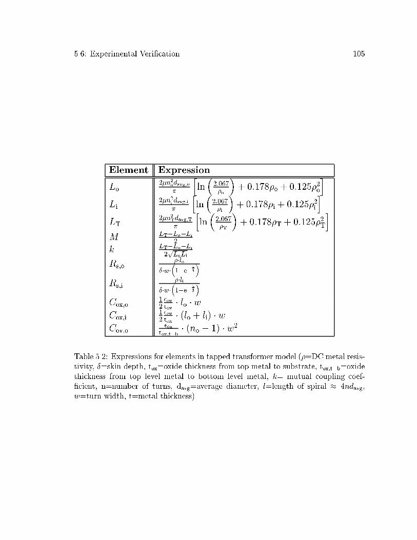
5.6: Experimental Veri�cation 105
Element Expression
Lo2�n2odavg;o
�
hln
�2:067�o
�+ 0:178�o + 0:125�2o
i
Li2�n2i davg;i
�
hln
�2:067�i
�+ 0:178�i + 0:125�2i
i
LT2�n2Tdavg;T
�
hln
�2:067�T
�+ 0:178�T + 0:125�2T
i
M LT�Lo�Li
2
k LT�Lo�Li
2pLoLi
Rs;o��lo
��w��1�e�
t�
�Rs;i
��li��w�
�1�e�
t�
�Cox;o
12�ox
tox� lo � w
Cox;i12�ox
tox� (lo + li) � w
Cov;o�ox
tox;t�b� (no � 1) � w2
Table 5.2: Expressions for elements in tapped transformer model (�=DC metal resis-
tivity, �=skin depth, tox=oxide thickness from top metal to substrate, tox;t�b=oxide
thickness from top level metal to bottom level metal, k= mutual coupling coef-
�cient, n=number of turns, davg=average diameter, l=length of spiral � 4ndavg,
w=turn width, t=metal thickness)

106 Chapter 5: Modeling and Characterization of On-Chip Transformers
Cov
Cox;t
Coxm
Cox;b
Rs;t
Rs;b
Ls;t
Ls;b
M
Terminal1
Terminal2
Figure 5.12: Stacked transformer model

5.6: Experimental Veri�cation 107
Element Expression
Lt2�n2tdavg;t
�
hln
�2:067�t
�+ 0:178�t + 0:125�2t
i
Lb2�n2bdavg;b
�
hln
�2:067�b
�+ 0:178�b + 0:125�2b
i
k 0:9� ds
davg
M kpLtLb
Rs;t�t�l
�t�w��1�e
�
tt�t
�Rs;b
�b�l
�b�w�
1�e
�
tb�b
!
Cov12
�ox
tox;t�b� l � w � Aov
A
Cox;t12�ox
tox;t� l � w � A�Aov
A
Cox;b12�ox
tox;b� l � w
Coxm Cox;t + Cox;b
Table 5.3: Expressions for elements in the stacked transformer model (�=DC
metal resistivity, �=skin depth, tox;t=oxide thickness from top metal to substrate,tox;b=oxide thickness from bottom metal to substrate, tox;t�b=oxide thickness from
top level metal to bottom level metal, k=mutual coupling coe�cient, n=number ofturns, davg=average diameter, l=length of spiral � 4ndavg, w=turn width, t=metal
thickness, A=area, Aov=overlapped area of top and bottom spirals, ds=center-to-
center spiral distance)

108 Chapter 5: Modeling and Characterization of On-Chip Transformers
S parameters
DUT
Coplanar GSG probes
HP8720B
network analyzer
50 environment
terminal 1 terminal 2
terminal 3
Figure 5.13: Experimental set up for measuring inductance
xs ys ds = dnorm = kpredict = kmeas
(�m) (�m)pxs2 + ys2 (
ds
AD) (0:9� dnorm)
A 0 0 0 0 0.9 0.88
B 8 8 11 0.09 0.81 0.79
C 42 0 42 0.35 0.55 0.57
D 57 0 57 0.48 0.42 0.45
E 50 50 71 0.59 0.31 0.28
Table 5.4: Comparison of transformer realizations.

5.6: Experimental Veri�cation 109
0.0 0.2 0.4 0.6 0.80.0
0.2
0.4
0.6
0.8
1.0
predicted kmeasured k
A
B
C
D
E
MutualCouplingCoe�cient(k)
dnorm
Figure 5.14: Coupling coe�cient (k) versus normalized shift (dnorm)
shifts. The stacked transformers are fabricated on the third and second layers of
a triple-metal 0:5�m CMOS epi-process with the patterned ground shields (PGS)
being implemented on the polysilicon layer. Each spiral has the following lateral
dimensions: dout = 180�m, w = 3:2�m, s = 2:1�m and n = 11:75. Figure 5.14 plots
the coupling coe�cient as a function of shift. Good agreement between measured
and modeled values of k is observed.
5.6.2 Veri�cation of Transformer Models
The measured S parameters of the device under test (DUT) are compared to the S
parameters predicted by our analytical model by the following procedure:
1. DUT : S-to-Y (YDUT)
2. Open calibration: S-to-Y (YO)
3. YCor = YDUT � YO

110 Chapter 5: Modeling and Characterization of On-Chip Transformers
4. YCor to Smeas
5. Compare Smeas to Scalc
The predictions of the analytical models were compared with measurements for a
variety of transformers.
Figure 5.15 compares the real and imaginary components of the measured S
parameters to those predicted by the analytical model for a tapped transformer.
This transformer was fabricated on a quartz substrate, and was designed to have
Lo = 3nH, Li = 2nH and k = 0:35. The �gure shows very good agreement between
simulated and measured results.
Fig. 5.16- 5.18 show good agreement for stacked transformers (Lt=20nH, Lb=20nH)
with various shifts (k=0.9, k=0.55, k=0.3). The stacked transformers are fabricated
on the third and second layers of a triple-metal 0:5�m CMOS epi-process with the
patterned ground shields (PGS) being implemented on the polysilicon layer. These
transformers correspond to the entries labeled A, C and E in table 5.4. Figure 5.16
compares the real and imaginary components of the measured S parameters to those
predicted by the analytical model for a stacked transformer with maximum overlap
(entry A). Figure 5.17 compares the same for a stacked transformer with top and
bottom spirals laterally shifted (entry C), while �gure 5.18 compares a stacked trans-
former with top and bottom spirals diagonally shifted (entry E). In every case, good
agreement is obtained between measurements and predictions of the model.
5.7 Summary
This chapter has explored how on-chip transformers may be modeled by lumped
circuit models whose elements have analytical expressions. The predictions of these
models compare well with measurement results.

5.7: Summary 111
� Tapped transformer on
quartz substrate
� dout;o = 290�m, no = 2:5
� dout;i = 190�m, ni = 4:25
� w = 13�m, s = 7�m
0.8 1.2 1.6 2.0 2.4Frequency (GHz)
-1.0
-0.5
0.0
0.5
1.0
S 21
real(S21) measimag(S21) measreal(S21) calcimag(S21) calc
0.8 1.2 1.6 2.0 2.4Frequency (GHz)
-1.0
-0.5
0.0
0.5
1.0
S 21
real(S21) measimag(S21) measreal(S21) calcimag(S21) calc
0.8 1.2 1.6 2.0 2.4Frequency (GHz)
-1.0
-0.5
0.0
0.5
1.0
S 21
real(S21) measimag(S21) measreal(S21) calcimag(S21) calc
Figure 5.15: Comparison of predicted and measured S parameters for a tapped
transformer

112 Chapter 5: Modeling and Characterization of On-Chip Transformers
� Stacked transformer with top
spiral overlapping bottom one
� dout = 180�m, n = 11:75,
w = 3:2�m, s = 2:1�m
� xs = 0�m, ys = 0�m,
ds = 0�m
0.0 0.5 1.0 1.5Frequency (GHz)
-1.0
-0.5
0.0
0.5
1.0
S 21
real(S21) measimag(S21) measreal(S21) calcimag(S21) calc
0.0 0.5 1.0 1.5Frequency (GHz)
-1.0
-0.5
0.0
0.5
1.0
S 11
real(S11) measimag(S11) measreal(S11) calcimag(S11) calc
0.0 0.5 1.0 1.5Frequency (GHz)
-1.0
-0.5
0.0
0.5
1.0
S 22
real(S22) measimag(S22) measreal(S22) calcimag(S22) calc
Figure 5.16: Comparison of predicted and measured S parameters for stacked trans-
former with top spiral overlapping bottom one

5.7: Summary 113
� Stacked transformer with top and
bottom spirals laterally shifted
� dout = 180�m, n = 11:75,
w = 3:2�m, s = 2:1�m
� xs = 42�m, ys = 0�m,
ds = 42�m
0.0 0.5 1.0 1.5Frequency (GHz)
-1.0
-0.5
0.0
0.5
1.0
S 21
real(S21) measimag(S21) measreal(S21) calcimag(S21) calc
0.0 0.5 1.0 1.5Frequency (GHz)
-1.0
-0.5
0.0
0.5
1.0
S 11
real(S11) measimag(S11) measreal(S11) calcimag(S11) calc
0.0 0.5 1.0 1.5Frequency (GHz)
-1.0
-0.5
0.0
0.5
1.0
S 22
real(S22) measimag(S22) measreal(S22) calcimag(S22) calc
Figure 5.17: Comparison of predicted and measured S parameters for stacked trans-
former with top and bottom spirals laterally shifted

114 Chapter 5: Modeling and Characterization of On-Chip Transformers
� Stacked transformer with top and
bottom spirals diagonally shifted
� dout = 180�m, n = 11:75,
w = 3:2�m, s = 2:1�m
� xs = 50�m, ys = 50�m,
ds = 71�m
0.0 0.5 1.0 1.5Frequency (GHz)
-1.0
-0.5
0.0
0.5
1.0
S 21
real(S21) measimag(S21) measreal(S21) calcimag(S21) calc
0.0 0.5 1.0 1.5Frequency (GHz)
-1.0
-0.5
0.0
0.5
1.0
S 11
real(S11) measimag(S11) measreal(S11) calcimag(S11) calc
0.0 0.5 1.0 1.5Frequency (GHz)
-1.0
-0.5
0.0
0.5
1.0
S 22
real(S22) measimag(S22) measreal(S22) calcimag(S22) calc
Figure 5.18: Comparison of predicted and measured S parameters for stacked trans-
former with top and bottom spirals diagonally shifted

Chapter 6
Design and Optimization of
Inductor Circuits
This chapter discusses the design and optimization of inductor circuits. Section 6.1
introduces common performance measures used to characterize on-chip inductors.
Particular attention is paid to various quality factor de�nitions and the conditions
under which a particular de�nition is relevant. Section 6.2 compares the optimum
performance achieved by square, hexagonal, octagonal and circular inductors. Sec-
tion 6.3 explores how inductors can enhance the bandwidth of broadband circuits
and presents a design methodology for optimizing on-chip inductors for such ap-
plications. Section 6.4 introduces geometric programming as a means of globally
optimizing inductor circuits quickly and e�ciently.
6.1 Parameters of Interest
This section describes the common performance parameters used to evaluate on-chip
inductors. Analytical expressions for these parameters can be obtained using the ele-
ments of the lumped circuit model described in chapter 2. However, these expressions
vary, depending on whether the inductor is used in a one terminal or two terminal
con�guration and on whether a patterned ground shield (PGS) is placed beneath the
115

116 Chapter 6: Design and Optimization of Inductor Circuits
inductor to eliminate the resistive and capacitive coupling to the substrate. This sec-
tion provides expressions for the performance parameters of an inductor with PGS
in a one terminal con�guration. This con�guration was chosen as most RF circuit
blocks (such as low noise ampli�ers and oscillators) use inductors as one terminal
devices, with the second terminal connected to a node that is at incremental ground.
Figure 6.1 shows the equivalent lumped circuit for this con�guration.
Cox + Cs
Rs
Ls
Figure 6.1: Lumped model for one terminal con�guration with PGS.
The most commonly quoted performance parameter is the quality factor, Q. The
de�nition of Q depends on the application. For most narrowband applications, it
is su�cient to de�ne the inductor quality factor, QL, and the tank quality factor,
Qtank.
� Inductor quality factor (QL) is de�ned as:
QL(!) = 2�[peak magnetic energy � peak electric energy]
energy loss in one oscillation cycle: (6.1)
An equivalent de�nition for QL is:
QL(!) =[Imaginary component of impedance:]
Real component of impedance: (6.2)

6.1: Parameters of Interest 117
For the one-terminal inductor shown in �gure 6.1, the inductor quality factor
is given by:
QL(!) =!Ls
Rs(!)
�1�
R2s (!)(Cox + Cs)
Ls
� !2Ls(Cox + Cs)
�(6.3)
QL is used in applications where the inductor's parasitic resistances as well
as capacitances degrade the circuit performance. An example where QL is
relevant is when an inductor is used as the source degeneration element in
narrowband low-noise ampli�ers [35, 2, 36]. QL is also pertinent in some �lter
applications.
� Tank quality factor (Qtank) is de�ned as:
Qtank(!) = 2�peak magnetic energy
energy loss in one oscillation cycle(6.4)
For the one-terminal inductor shown in �gure 6.1, the tank quality factor is
given by:
Qtank(!) =!Ls
Rs(!)(6.5)
This de�nition is appropriate when only the inductor's parasitic resistances
degrade the overall circuit performance. In such cases, the parasitic capaci-
tance of the inductor is incorporated as part of the resonance network. This
de�nition applies in every case where the on-chip inductor is used as part of
a resonant tank circuit (hence the term Qtank). The best examples of such
circuits are resonators and oscillators where the resonance tank occurs at the
drain of MOSFET (or equivalently, the collector of a BJT) [37, 2, 37, 4].

118 Chapter 6: Design and Optimization of Inductor Circuits
� Self-resonant frequency (!res) is de�ned the frequency at which QL = 0.
Beyond this frequency, the inductor exhibits a negative reactance thereby ren-
dering it useless as an inductive tuning element. In most on-chip spiral induc-
tors, QL reaches a maximum at around half the self-resonant frequency. On
the other hand, Qtank typically reaches a maximum close to !res.
6.2 Comparison of Inductor Geometries
This section compares the optimum one terminal QL achieved using square, hexago-
nal, octagonal and circular spirals for a �xed inductance at a given frequency. Note
that degradation due to magnetic coupling to the substrate is not considered in this
treatment. This issue is discussed in 7.
6.2.1 Example: Maximum QL @ 2GHz for L = 8nH
Figure 6.2 compares the maximum QL achieved at 2GHz by the various spiral ge-
ometries for a 8nH inductor. The same process parameters are used for all the
polygonal spirals so that the vertical parameters of the spiral are held constant. The
lateral geometrical parameters (w, s, n and dout) are optimized to yield a �xed series
inductance, L of 8nH with maximum QL at 2GHz.
Table 6.2.1 summarizes the outer diameter and area of the optimum spirals. For
polygons with more than four sides, the inductor area is less than the e�ective chip
area. The e�ective chip area is de�ned as the area of the smallest square within
which the polygonal spiral may be inscribed. For example, for a circular spiral with
an outer diamter of dout, the inductor area is 0:25�d2out whereas the e�ective chip
area is d2out. In general, the e�ective chip area is the more relevant metric as it is a
measure of how much area is dedicated on-chip to a spiral inductor. For example,
if one considers an octagonal spiral, the di�erence between its inductor area and its
e�ective area is the sum of the four triangular areas which lie outside its four sides
that are at an angle of pi=4 radians to the sides of the square within which the spiral
is inscribed. In most circuit layouts, these four triangular areas are not used for any

6.2: Comparison of Inductor Geometries 119
SquareHexagonalOctagonalCircular
1
1
2
2
3
3
4
4
0
0
5
6
QL
Frequency (GHz)
Figure 6.2: Comparison of maximum QL @ 2GHz for L = 8nH

120 Chapter 6: Design and Optimization of Inductor Circuits
other purpose and therefore must be included in the area dedicated to the spiral.
Thus, the e�ective chip area is best de�ned as the smallest square area within which
a given spiral �ts.
Layout Outer Inductor E�ective
diameter area chip area(�m) mm2 mm2
Square 287 0.082 0.082Hexagonal 308 0.082 0.095
Octagonal 309 0.079 0.095
Circular 314 0.077 0.099
Table 6.1: Outer diameter and area of inductors with maximum QL @ 2GHz forL = 8nH
Using the e�ective area as a reference, it is clear that the square spiral is most
area e�cient whereas the circular spiral is least area e�cient. However, the circular
spiral achieves the best QL. In general, circular spirals consume around 20% more
chip area than square spirals and achieve QL values that are � 15� 20% better.
As expected, the performance of hexagonal and octagonal geometries is between
that of square and circular ones. The plot suggests that an octagonal spiral achieves
QL values that are within � 3� 5% of that of a circular one with a corresponding
� 3 � 5% reduction in the e�ective chip area. This suggests that polygons with
more than eight sides are not needed for most applications, thereby minimizing the
layout complexity.
6.2.2 Example: Maximum QL @ 3GHz for L = 5nH
Figure 6.3 compares the maximum QL achieved at 2GHz by the various spiral ge-
ometries for a 8nH inductor. Table 6.2 summarizes the outer diameter and area
of the optimum spirals. Once again, QL and the e�ective chip area increase with
the number of sides of the spiral. There is a striking resemblance between the per-
formance comparison of the previous example and this one. Since the frequency

6.2: Comparison of Inductor Geometries 121
SquareHexagonalOctagonalCircular1
1
2
2
3
3
4
4
0
0
5
5
6
7
QL
Frequency (GHz)
Figure 6.3: Comparison of maximum QL @ 3GHz for L = 5nH

122 Chapter 6: Design and Optimization of Inductor Circuits
Layout Outer Inductor E�ectivediameter area chip area
(�m) mm2 mm2
Square 288 0.083 0.083Hexagonal 309 0.083 0.095
Octagonal 310 0.080 0.096
Circular 315 0.078 0.099
Table 6.2: Outer diameter and area of inductors with maximum QL @ 3GHz for
L = 5nH
is higher and the speci�ed inductance lower, the optimal QL is higher for a given
geometry when compared to the previous example.
6.2.3 Maximum QL for L = 5nH with dout = 300�m
Figure 6.4 compares the maximum QL achieved at the various spiral geometries
for a 5nH subject to the constraint that the maximum outer diamter be 300�m.
Table 6.3 summarizes the dimensions of the optimum spirals. The addition of the
Layout dout davg w s n �
(�m) (�m) (�m) (�m) n �
Square 300 229 17.6 2 3.75 0.31
Hexagonal 300 229 16.2 2 4.00 0.31
Octagonal 300 230 16.1 2 4.00 0.31
Circular 300 232 15.5 2 4.00 0.29
Table 6.3: Dimensions of inductors with maximum QL for L = 5nH with dout =
300�m
area constraint permits us to compare the maximum QL achievable by the various
geometries for a �xed e�ective chip area. Now, the QL of the circular spiral is
larger than the square spiral by � 10% at the (�xed) frequency of interest. Note
however, that the circular spiral reaches its maximum QL at a higher frequency than

6.2: Bandwidth Extension in Broadband Circuits 123
SquareHexagonalOctagonalCircular1
1
2
2
3
3
4
4
0
0
5
5
6
7
8
QL
Frequency (GHz)
Figure 6.4: Comparison of maximum QL for L = 5nH with dout = 300�m

124 Chapter 6: Design and Optimization of Inductor Circuits
the square one. This observation is consistent with the results of the previous two
examples.
6.3 Bandwidth Extension in Broadband Circuits
Although inductors are commonly associated with narrowband circuits, they are
useful in broadband circuits as well. In this section we examine how an inductor
can be used to enhance the bandwidth of a simple ampli�er. We then study how
an on-chip inductor can be designed to optimize the performance of this broadband
ampli�er.
6.3.1 Shunt-peaked Ampli�cation
We illustrate the use of inductors for extending the bandwidth of broadband circuits
by considering the simple common source ampli�er illustrated in �gure 6.5(a). For
simplicity, we assume that the small signal frequency response of this ampli�er is
dominated by the output pole whose value is determined solely by load resistance,
R, and the load capacitance, C (�gure 6.5(b)):
vout
vin(!) =
gmR
1 + j!RC: (6.6)
The introduction of an inductance, L, in series with the load resistance alters
the frequency response of the ampli�er (�gure 6.5(c)). This technique, called shunt-
peaking, enhances the bandwidth of the ampli�er by transforming the frequency
response from that of a single pole to one with two poles and a zero ( �gure 6.5(d))):
vout
vin(!) =
gm(R + j!L)
1 + j!RC � !2LC(6.7)
The poles may or may not be complex (although, they are complex for practical cases
of bandwidth extension). The zero is determined solely by the L=R time constant,
and is primarily responsible for the bandwidth enhancement.

6.3: Bandwidth Extension in Broadband Circuits 125
R
C
Vdd
vout
vin
(a)
R C
vout
gmvin
(b)
L
R
C
Vdd
vout
vin
(c)
L
R
C
vout
gmvin
(d)
Figure 6.5: Shunt-peaking in a common source ampli�er. (a) Simple common source
ampli�er, and (b) its equivalent small signal model. (c) Common source ampli�er
with shunt peaking and (d) its equivalent small signal model.

126 Chapter 6: Design and Optimization of Inductor Circuits
Factor (m) Normalized !3dB Response
0 1:00 No shunt peaking
0:32 1:60 Optimum group delay
0:41 1:72 Maximally at
0:71 1:85 Maximum bandwidth
Table 6.4: Benchmarks for shunt peaking
The frequency response of the shunt peaked ampli�er is characterized by the ratio
of the L=R and RC time constants. This ratio is denoted by m where L = mR2C.
Figure 6.6 illustrates the frequency response of the shunt peaked ampli�er for various
values of m. The frequency and magnitude axes have been normalized so that the
low frequency gain is unity and so that the 3dB bandwidth for the case with no
shunt peaking (m = 0) is unity (RC = 1). The frequency response is plotted for the
values of m listed in table 6.4 [34]. As expected, the 3dB bandwidth increases as m
increases. The maximum bandwidth is obtained when m = 0:71 and yields an 85%
improvement in bandwidth. However, as can be clearly seen in the magnitude plot,
this comes at the cost of signi�cant gain peaking. A maximally at response may
be obtained for m = 0:41 with a still impressive bandwidth improvement of 72%.
Another interesting case occurs when m = 0:32. As seen in the phase plot, this
best approximates a linear phase response up to the 3dB bandwidth, which is 60%
higher than the case without shunt peaking. This case is called the `optimum group
delay case' and is desirable for optimizing pulse �delity in broadband systems that
transmit digital signals.
The next section will explore how on-chip inductors can be optimized for use in
shunt-peaked ampli�ers.
6.3.2 On-Chip Shunt-Peaking
The non-idealities of on-chip inductors present several challenges for implementing
shunt-peaked ampli�ers on-chip. The biggest issue is the reduction in bandwidth

6.3: Bandwidth Extension in Broadband Circuits 127
No peakingOptimum group delayMaximally flatMaximum bandwidth
0 0:20:4
0:4
0:5
0:6
0:6
0:7
0:8
0:8
0:9
1:0
1:0
1:1
1:2 1:4 1:6 1:8 2:0Normalized frequency
Magnitude
No peakingOptimum group delayMaximally flatMaximum bandwidth
0
0 0:2 0:4 0:6 0:8 1:0 1:2 1:4 1:6 1:8 2:0
�10
�20
�30
�40
�50
�60
�70
�80
�90
Normalized frequency
Phase
Figure 6.6: Frequency response of shunt-peaked cases tabulated in table 6.4.

128 Chapter 6: Design and Optimization of Inductor Circuits
Vdd
L
(R� Rs)
Rs
vout
vin
Cg
CL
Cd Cload
Figure 6.7: Shunt-peaking with optimized on-chip inductor

6.4: Optimization via Geometric Programming 129
improvement because of the additional parasitic capacitance introduced by the in-
ductor. Figure 6.7 illustrates how this capacitance can be minimized by paritioning
the total load resistance, R, between the inductor's series resistance (Rs) and the
external resistance, which now takes on the value of (R � Rs). Since the series
resistance is now part of the load resistance, the quality factor of the inductor is
largely irrelevant and therefore the inductor's turn width, w, can be made small to
permit the desired inductance to be realized while minimizing the spiral area and
capacitance. In this case, the minimum w is determined in part by current density
limitations as the transistor current also ows through the inductor. The minimum
turn spacing, s, is usually set by lithography limitations.
The desired inductance is now a function of both the transistor's and inductor's
parasitics as well as the load capacitance and external resistance. Thus the opti-
mization of on-chip shunt-peaking requires the simultaneous optimization of passive
and active components. This scenario accentuates the limitations of using a �eld
solver for modeling the inductor. Even if the �eld solver contains a general purpose
optimization routine, it serves no use as the performance parameters of the inductor
alone (such as QL) cannot specify the optimization goal. Therefore, several itera-
tions would be needed (each requiring an interface between the �eld solver and the
circuit simulator), before an acceptable design could be obtained.
On the other hand, a lumped circuit model (with analytical expressions for all
the elements in terms of the spiral's geometrical parameters and process parameters)
can be easily incorporated into a circuit simulator and thereby provide a way for the
designer to optimize the entire circuit. Thus the inductance expressions discussed
in chapter 4 serve as a valuable design tool when combined with the lumped circuit
model described in chapter 2.
The use of on-chip shunt peaking is attractive for a variety of broadband ap-
plications as it gives better performance with no additional power dissipation. Ap-
pendix C illustrates how optimized on-chip spiral inductors can be used as shunt-
peaking elements to increase the transimpedance of a preampli�er intended as the
front-end of a gigabit optical receiver.

130 Chapter 6: Design and Optimization of Inductor Circuits
6.4 Optimization via Geometric Programming
Although the availability of simple inductance expressions and lumped models al-
lows engineers to design and optimize inductor circuits in a circuit environment
such as SPICE, this process can be time consuming. The main reason is that CAD
tools built around circuit solvers employ general purpose optimization tools that are
slow. Furthermore, these tools can usually identify only local optima. Typically,
most designers do variable sweeps over multiple dimensions (guided by prior design
knowledge and insight) to arrive at an acceptable design. In such cases, the number
of iterations increases exponentially with the number of variables. Considering that
a planar spiral inductor has four geometrical parameters, it is clear that the simul-
taneous optimization of active and passive components can only be carried out for
circuits with a couple of transistors and inductors.
This section introduces an e�cient method for the optimal design and synthesis
of RF CMOS inductor circuits. The method is based on geometric programming.
This method is attractive as it quickly generates a design that is globally optimal
for a given set of speci�cations and constraints. Moreover, when no solution exists
for a problem, this method unambiguously declares infeasibility.
6.4.1 Geometric Programming
Let f be a real-valued function of n real, positive variables x1; x2; : : : ; xn. It is called
a posynomial function if it has the form
f(x1; : : : ; xn) =
tXk=1
ckx�1k1 x�2k2 � � �x�nk
n
where cj� 0 and �
ij2 R. When t = 1, f is called a monomial function. Thus,
for example, 0:7 + 2x1=x23 + x0:32 is posynomial and 2:3(x1=x2)
1:5 is a monomial.
Posynomials are closed under sums, products, and nonnegative scaling.

6.4: Optimization via Geometric Programming 131
A geometric program (GP) ) has the form
minimize f0(x)
subject to fi(x) � 1; i = 1; 2; : : : ; m;
gi(x) = 1; i = 1; 2; : : : ; p;
xi> 0; i = 1; 2; : : : ; n;
(6.8)
where fiare posynomial functions and g
iare monomial functions. If f is a posyn-
omial and g is a monomial, then the constraint f(x) � g(x) can be expressed as
f(x)=g(x) � 1 (since f=g is posynomial). From closure under non-negativity, con-
straints of the form f(x) � a, where a > 0 can also be used. Similarly, if g1 and
g2 are both monomial functions, the constraint g1(x) = g2(x) can be expressed as
g1(x)=g2(x) = 1 (since g1=g2 is monomial).
The key to solving GPs is a change of variables that converts the posynomial
objective and constraint functions into convex functions of the new variables. We
de�ne new variables yi= logx
i, and take the logarithm of a posynomial f to get
h(y) = log (f (ey1 ; : : : ; eyn)) = log
tXk
eaT
ky+bk
!
where aTk= [�1k � � ��nk
] and bk= log c
k. It can be shown that h is a convex function
of y. This transformation converts the standard geometric program (6.8) into the
convex optimization program:
minimize log f0(ey1; : : : ; eyn)
subject to log fi(ey1 ; : : : ; eyn) � 0; i = 1; : : : ; m
log gi(ey1 ; : : : ; eyn) = 0; i = 1; : : : ; p;
(6.9)
which is called the convex form of the geometric program. Even though this problem
is highly nonlinear, it can be solved globally and very e�ciently by recently developed
interior-point methods [39].
For our purposes, the most important feature of geometric programs is that they
can be globally solved with great e�ciency. Such solution algorithms also determine

132 Chapter 6: Design and Optimization of Inductor Circuits
whether the problem is infeasible. Also, the starting point for the optimization
algorithm does not have any e�ect on the �nal solution; indeed, an initial starting
point or design is completely unnecessary.
Many circuit problems may be posed as geometric programs [28, 40]. In particu-
lar, the design speci�cations of inductor circuits can be formulated in a way suitable
for geometric programming [41, 42]. The application of geometric programming in
analog circuit design is discussed in detail in the Ph.D. thesis of Maria del Mar
Hershenson [40].
6.5 Summary
This chapter described how inductors can be optimally designed for use in inductor
circuits. Section 6.1 introduces common performance measures used to characterize
on-chip inductors. Various quality factor de�nitions were presented and the appro-
priate conditions for their use was identi�ed. The optimum performance achieved by
square, hexagonal, octagonal and circular inductors were compared. Techniques for
extending the bandwidth of broadband circuits using inductors as shunt-peaking el-
ements were presented. Particular attention was paid to the optimization of on-chip
inductors used for shunt-peaking. Finally, a new and e�cient method for optimizing
inductors, based on geometric programming was introduced.

Chapter 7
Magnetic Coupling from Spiral to
Substrate
The performance of an on-chip spiral inductor is degraded by resistive, capacitive
and inductive coupling to a conductive substrate. The resistive and capacitive cou-
pling mechanisms have been well understood and modeled as discussed in chapter 2.
Furthermore, the patterned ground shield (PGS) can be used to eliminate these ef-
fects. On the other hand, the magnetic coupling to the substrate has not been well
understood. Although this mechanism is known to limit the performance of induc-
tors built on the high conductivity substrate processes typical of modern CMOS, no
simple models exist to provide design guidance.
In this chapter, we will study how magnetic coupling from an on-chip spiral to
the silicon substrate a�ects the performance of an inductor. Section 7.1 develops a
current sheet based approach for modeling the magnetic coupling to the substrate.
This model provides valuable design insight and quanti�es the degradation in induc-
tor performance as a function of frequency, substrate conductivity, and the spiral
and process parameters. The predictions of this model agree well with experimental
results as demonstrated in section 7.2.
133

134 Chapter 7: Magnetic Coupling from Spiral to Substrate
Rs
Ls
Msub
Rsub
Lsub
Figure 7.1: Circuit model of inductor with substrate magnetic coupling
7.1 Modeling of Substrate Magnetic Coupling
The e�ect of substrate magnetic coupling on an inductor is modeled with a trans-
former as indicated in Figure 7.1. Rs and Ls are the series resistance and inductance
of the spiral inductor, Msub is the mutual inductance between the spiral and sub-
strate, and Rsub and Lsub are the substrate resistance and inductance associated
with eddy current ow. Thus, the equivalent impedance between the two ports of
the inductance is Z(!) where
Z(!) = Rs + j!Ls +
�!2M2
sub
Rsub + j!Lsub
�: (7.1)
The substrate coupling is therefore re ected at the terminals of the inductor as
an increase in the series resistance and a decrease in the inductance, both of which
degrade performance. Figure 7.1 shows the equivalent one-port model. The e�ective
resistance, Re� , and e�ective inductance, Le� , are:
Re� = Rs +Rsub
�!2M2
sub
R2sub + !2L2
sub
�(7.2)

7.1: Modeling of Substrate Magnetic Coupling 135
Re� = Rs + Rsub
�!2M
2sub
R2sub+!
2L2sub
�Le� = Ls � Lsub
�!2M
2sub
R2sub+!
2L2sub
�
Figure 7.2: Equivalent circuit model
Le� = Ls � Lsub
�!2M2
sub
R2sub + !2L2
sub
�(7.3)
Thus, magnetic coupling to the substrate reduces the inductance and increases the
series resistance.
7.1.1 Simplifying Approximations
Clearly, a small Msub, large Rsub and large Lsub are desired to minimize the adverse
e�ects of magnetic coupling to the substrate. Unfortunately, the distributed, three
dimensional nature of the substrate makes it di�cult to accurately modelMsub, Rsub
and Lsub. This di�culty is exacerbated by the fact that the substrate conductiv-
ity can change by a factor of 2-3 or more from process variations and with depth.
Furthermore, temperature variations can change the substrate conductivity by al-
most an order of magnitude. This section �rst presents a qualitative overview of the
variables and then simpli�es the problem by using approximations that are valid for
current silicon substrates.
As one may expect, Msub and Rsub are dependent on the skin depth of the
substrate as well as the parameters of the spiral. The toughest parameter to model
is Lsub. Since the maximum substrate conductivity is � 104Sm�1, and therefore
three orders of magnitude smaller than that of metals, it is safe to assume that

136 Chapter 7: Magnetic Coupling from Spiral to Substrate
the resistive term (Rsub) associated with the eddy currents completely dominates
the corresponding inductive term (Lsub) for frequencies up to 10GHz. Since these
terms are in series, the denominator of equation 7.1 may be approximated by Rsub+
j!Lsub � Rsub, yielding simpler expressions for the elements in �gure 7.2:
Re� � Rs +
�!2M2
sub
Rsub
�(7.4)
Le� � Ls (7.5)
Thus the primary e�ect of magnetic substrate coupling is an increase in the series
resistance. The following sections develop approximate expressions for Msub and
Rsub permitting Re� to be quanti�ed.
7.1.2 E�ective Substrate Skin Depth
The skin depth of the substrate, �sub, decreases as the frequency and substrate
conductivity increase:
�sub =
r2
�!�sub: (7.6)
Equation 7.6 de�nes the skin depth of an in�nitely thick substrate. For a substrate
with �nite thickness, tsub, the e�ective skin depth, dsub, is given by:
dsub = �sub
�1� e
(�tsub
�sub
)
�: (7.7)
The e�ective depth approaches �sub
when the skin depth is much smaller than the
substrate thickness. This is the typical operating regime at gigahertz frequencies
for epi-processes, as typical silicon substrate thicknesses range from 300 � 700�m.
For example, modern epitaxial processes have conductivities of 104Sm�1 giving a
�sub of 160�m at 1GHz and 70�m at 5GHz. For a substrate thickness of 300�m,
the corresponding e�ective skin depth is 135�m at 1GHz and 69�m at 5GHz. Since

7.1: Modeling of Substrate Magnetic Coupling 137
Msub and Rsub become signi�cant as dsub becomes small, we may safely assume that
dsub � �sub in the region of interest.
For bulk processes, the substrate conductivity is typically very low (� 10Sm�1)
and therefore the e�ective skin depth must be used. However in this case, the
magnetic coupling to the substrate can be neglected precisely because of this low
conductivity.
The next section will consider how Msub and Rsub can be estimated for an epi-
process.
7.1.3 Computation of Msub and Rsub
Figure 7.3 illustrates the cross section of a spiral inductor on an epi-process. The
epi-layer is typically 3� 10�m thick and has very low conductivity (10� 100Sm�1)
and therefore negligible eddy current ow. The substrate layer is highly conductive
(103 � 104Sm�1) and can support large eddy currents.
The exact computation of the eddy current density is di�cult. We simplify
the problem by treating the spiral inductor as an equivalent current sheet and by
assuming that the substrate eddy currents ow in a current block directly below the
current sheet. Figure 7.4 illustrates this approximation. The current density in the
substrate block decreases with increasing depth because of two e�ects:
1. the skin e�ect in the substrate causes the induced current density to roll o�
exponentially with increasing depth
2. the induced currents depend on the magnetic �eld of the spiral inductor. This
magnetic �eld decays as the distance from the spiral increases
We assume that the eddy current density at a given depth is proportional to the
product of:
1. the exponential decay due to the substrate skin e�ect so that:
Isub;fact1(zsub) /1
�subexp
��zsub�sub
�(7.8)

138 Chapter 7: Magnetic Coupling from Spiral to Substrate
dout
din �davg�davg
tm
tox
tepi
tsub
oxide
epi� layer
substrate
Figure 7.3: Cross section of an epi-process

7.1: Modeling of Substrate Magnetic Coupling 139
dout
din �davg�davg
tm + tox
tepi
tsub
oxide
epi� layer
substrate
current sheetcurrent sheet
current blockcurrent block
Figure 7.4: Current sheet and current block approximations

140 Chapter 7: Magnetic Coupling from Spiral to Substrate
and
2. the mutual inductance between the spiral's equivalent current sheet and an
equivalent current sheet placed at depth zsub:
Isub;fact12(zsub) /Msubsheet(zsub): (7.9)
The factor Msubsheet(zsub) is calculated using the theory developed for current
sheets in chapter 3. Note that Msubsheet(zsub) is dependent on the parameters of the
spiral inductor (which for the current sheet approximation are the number of turns,
n, the average diameter, davg and the �ll factor, �) as well as the total distance
of separation, which is equal to (tm + tox + tepi + zsub). The total e�ective mutual
inductance between the spiral and the substrate, Msub, is obtained by taking a
weighted average of Msubsheet(zsub) over all values of zsub:
Msub �
Rtsub
0Msubsheet(zsub)Isub;fact1(zsub)Isub;fact2(zsub)dzR
tsub
0Isub;fact1(zsub)Isub;fact2(zsub)dz
: (7.10)
Msub increases as tm,tox,tepi, �sub and � decrease and as davg and n increase. An ap-
proximate expression forMsub is obtained by evaluating the integrals in equation 7.10
over a wide design space and data-�tting:
Msub ��ndavg
2���0:2z�0:3n;insz
�0:2n;sub: (7.11)
In this expression, zn;ins = (tm + tox + tepi)=davg and zn;sub = �sub=davg. Thus, zn;ins
is the ratio of the total thickness of the insulating layers to the spiral's average
diameter and zn;sub is the ratio of the substrate skin depth to the spiral's average
diameter. This expression has a worst case of error of 10% with respect to the value
predicted by equation 7.10.
The resistance Rsub is dependent on the e�ective length, width and thickness of
the substrate as well as the conductivity of the substrate. The e�ective length and
width for the current block approximation are 4davg and �davg, respectively. The
e�ective thickness is obtained from considering the current density distribution as

7.1: Modeling of Substrate Magnetic Coupling 141
a function of depth. Applying the same assumption used in the calculation of Msub
(namely that the current distribution is proportional to Isub;fact1(zsub)Isub;fact2(zsub)),
we obtain an approximate expression for the e�ective thickness:
tsub;e� � e�1davg�0:1z0:05n;insz
0:5n;sub: (7.12)
Thus, Rsub evaluates to:
Rsub �lengthsub;e�
�subwsub;e�tsub;e��
4e
�subdavg��1:1z�0:05n;ins z
�0:5n;sub: (7.13)
As one expects, the e�ective resistance of the substrate decreases as the �, zn;ins and
zn;sub increases and as davg decreases.
7.1.4 Increase in Resistance Due to Magnetic Coupling to
the Substrate
The equivalent re ected resistance due to magnetic coupling to the substrate is
obtained by combining equations 7.11 and 7.13:
Req;re sub ��!2M2
sub
Rsub
��
�sub
4e
�!�n2�
�2d3avg�
0:7z�0:55n;ins z0:1n;sub: (7.14)
Since this expression is obtained using several approximations, its accuracy is lim-
ited. Nevertheless, the expression provides valuable design insight as it identi�es
the relative e�ect of inductor and process parameters on the energy coupled to the
substrate. In particular, note that the re ected resistance is proportional to the
cube of the average diameter, the square of the frequency and to the square of the
number of turns. We pointed out earlier that magnetic coupling from the substrate
to the spiral can be thought of as a transformer with the spiral in the primary, the
substrate resistance, Rsub, as the load of the secondary and the substrate-to-spiral
mutual inductance, Msub, as the mutual inductance between the primary and the
secondary. This suggests that the load of the secondary, when re ected to the pri-
mary, looks like a resistance, Req;re sub, that is equal to the square of the impedance

142 Chapter 7: Magnetic Coupling from Spiral to Substrate
of Msub divided by Rsub. Since the impedance of Msub is simply !Msub, we expect
Req;re sub to be proportional to !2. Furthermore, since the mutual inductance Msub,
just like the spiral's self inductance, is proportional to the spiral's average diame-
ter, davg, and the substrate resistance is inversely proportional to davg, the re ected
impedance Req;re sub is proportional to the cube of davg.
7.2 Measurements
The predictions of the substrate model were compared to measurement results for a
0:5�m CMOS epi-process with a 7�m epi layer with a conductivity of 33Sm�1 and a
bulk conductivity of 104Sm�1. The spirals were designed for use in a GPS receiver
so that the frequency of interest was centered at 1:575GHz. A PGS was placed
beneath each spiral so that only magnetic coupling to the substrate would degrade
the e�ective resistance. The results are displayed for four spirals in �gures 7.5- 7.8.
In each case, the top �gure plots Rs, Req;re sub and Re� versus frequency. The
resistance plots clearly show that the e�ective series resistance is dominated by the
magnetic coupling to the substrate at high frequencies.
The lower �gure compares the measured and predicted inductor quality factor
(QL) when only Rs and Re� are individually considered. The predictions based on
Re� show better agreement with measurements (compared to the predictions based
on Rs) for all four spirals con�rming the importance of modeling magnetic coupling
to the substrate.
7.3 Summary
This chapter studied the e�ect of magnetic coupling from an on-chip spiral to the
substrate. A simple model was developed to estimate this e�ect's impact on per-
formance. While the inductance is not a�ected signi�cantly, this e�ect dominates
the e�ective series resistance at high frequencies for modern CMOS-epi processes
whose bulk substrate conductivities are 103�104Sm�1. Measurements indicate that
the simple model correctly estimates the increase in the e�ective series resistance

7.3: Summary 143
1
2
2 3
4
00
6
8
10
12
Resistance()
Frequency (GHz)
Re�
Req;re sub
Rs
8
9
10
1
1
2
2
3
3
4
00
5
6
7
QL
Frequency (GHz)
QL using Re�
QL using Rs
Measured
Figure 7.5: Impact of magnetic coupling on series resistance and inductor Q (QL)
for square spiral with dout = 345�m, w = 22:4�m, s = 2:1�m and n = 3:75.

144 Chapter 7: Magnetic Coupling from Spiral to Substrate
1
2
2 3
4
00
6
8
10
12
14
Resistance()
Frequency (GHz)
Re�
Req;re sub
Rs
1
1
2
2
3
3
4
00
5
6
7
8
9
10
QL
Frequency (GHz)
QL using Re�
QL using Rs
Measured
Figure 7.6: Impact of magnetic coupling on series resistance and inductor Q (QL)for square spiral with dout = 325�m, w = 21:0�m, s = 2:1�m and n = 4:25.

7.3: Summary 145
1 2 300
5
10
15
20
Resistance()
Frequency (GHz)
Re�
Req;re sub
Rs
1
1
2
2
3
3
4
00
5
6
7
8
QL
Frequency (GHz)
QL using Re�
QL using Rs
Measured
Figure 7.7: Impact of magnetic coupling on series resistance and inductor Q (QL)for square spiral with dout = 300�m, w = 12:0�m, s = 2:1�m and n = 5:25.

146 Chapter 7: Magnetic Coupling from Spiral to Substrate
1
2
2 3
4
00
6
8
10
12
14
Resistance()
Frequency (GHz)
Re�
Req;re sub
Rs
1
1
2
2
3
3
4
400
5
6
7
8
QL
Frequency (GHz)
QL using Re�
QL using Rs
Measured
Figure 7.8: Impact of magnetic coupling on series resistance and inductor Q (QL)for square spiral with dout = 240�m, w = 12:0�m, s = 2:1�m and n = 5:75.

7.3: Summary 147
to within 20%. More important, the model provides design insight on how a spi-
ral could be optimized so as to minimize degradation to magnetic coupling to the
substrate.
As higlighted during the discussion of equation 7.14, the resistive loss term arising
from magnetic coupling to the substrate is proportional the cube of the average
diameter, davg. Clearly, minimizing the average diameter is paramount. However,
this reduction in davg should not a�ect the value of the inductance nor the series
resistance of the spiral's conductor. One possible solution is to use a series connected
stack of spirals to achieve a higher inductance density thanks to the boost provided
by the mutual inductance between the stacked spirals. Chapter 5 discussed stacked
spiral con�gurations and pointed out that the maximum achievable mutual coupling
coe�cient, k, is around 0:9. This corresponds to an increase in inductance density of
2(1+k) = 3:6 if one uses two stacked spirals with maximum overlap. Assuming that
the two spirals are built on metal layers of equal conductivities, this would result in
a factor of two increase in the interconnect's series resistance. For a �xed inductance
and interconnect series resistance, the area of the stacked spiral is a factor of � 1:9
smaller than that of a single layer implementation. Therefore its davg is a factor of
�p1:9 smaller than that of a single layer spiral. This suggests that the increase in
resistance due to magnetic coupling to the substrate can be reduced by a factor of
� 2�3 by using two layer stacked spirals, implying signi�cant Q boosts are possible.
The drawback of the stacked spiral is the reduction in the self-resonant frequency
due to the increase in parasitic capacitance. While the dominant capacitance of a
single layer implementation is the spiral-to-substrate capacitance, the stacked spiral's
capacitance is typically dominated by the capacitance between the stacked spirals.
Furthermore, the capacitance density from the spiral-to-substrate increases because
the use of multiple layers reduces the distance between the spiral and the substrate.
This increase in capacitance density is partially o�set by the reduction in the area
of a stacked spiral. It is this reduction in self-resonant frequency that limits the
optimum number of stacked spirals to two or three. More work is needed to quantify
and compare the performance improvement a�orded by stacked spirals.

148 Chapter 7: Magnetic Coupling from Spiral to Substrate
Chapter 8
Conclusion
This thesis has investigated the design and modeling of on-chip spiral inductors and
transformers. This chapter summarizes the major contributions of this work and
identi�es areas that merit future study.
8.1 Contributions
� A current sheet approach was developed that permits simple, accurate expres-
sions to be derived for the inductance of commonly used conductor geometries.
� Simple, accurate expressions were derived for the inductance of on-chip planar
spirals. These expressions, which exhibit typical errors of� 2�4% with respect
to simulations of �eld solvers and measured data, are easily incorporated into
existing lumped circuit inductor models.
� Techniques for calculating the mutual inductance and the mutual coupling
coe�cient of single layer and two-layer planar on-chip transformers were pre-
sented. These techniques, based on the current sheet approach and the induc-
tance expressions mentioned above, yield simple, accurate, analytical expres-
sions for the mutual inductance and mutual coupling coe�cient.
149

150 Chapter 8: Conclusion
� A general approach to modeling planar, on-chip transformers using a scalable,
lumped circuit model was studied for both single layer and multiple layer imple-
mentations. The predictions of these models agree well with measurements.
The lumped circuit transformer models provide valuable design insight and
can easily be incorporated into a standard circuit design environment (such as
SPICE )
� The simple inductance expressions were applied in circuit design problems to
quickly and easily evaluate the optimum inductor designs. The availability
of these expressions allows the user to simultaneously optimize both passive
and active components, thereby facilitating the design of a variety inductor
circuits including low-noise ampli�ers (LNAs), oscillators, matching networks
and �lters.
� An area and power e�cient technique was developed for extending the band-
width of broadband ampli�ers by using optimized on-chip inductors as shunt-
peaking elements. This technique was applied to the implementation of a
transimpedance preampli�er designed as the front-end of a gigabit optical com-
munication system. This preampli�er is the �rst CMOS implementation that
uses planar spiral inductors as shunt-peaking elements.
� Magnetic coupling between a planar spiral inductor and the substrate was
studied. A simpli�ed current sheet based approximation yielded valuable in-
sight on the nature of this interaction and identi�ed the critical geometrical
and process parameters associated with this coupling. A simple, approximate
expression was developed to provide design guidelines. This work serves as a
good foundation for incorporating magnetic coupling to the substrate into a
lumped circuit inductor model.
While the current sheet approach forms the theoretical basis for this thesis, the
accurate inductance expressions and transformer models presented are valuable de-
sign tools for any practicing circuit designer. All in all, the contributions of this work

8.2: Future Work 151
substantially reduce the time required to optimize monolithic inductor circuits, by
eliminating the need for a �eld solver during the initial design stages.
8.2 Future Work
This sections identi�es topics covered in this thesis which merit more detailed study.
8.2.1 Magnetic Coupling to the Substrate
Chapter 7 investigated the e�ect of magnetic coupling between a spiral inductor and
a lossy substrate. This study provided valuable design insight and identi�ed the
major design parameters that in uence the severity of this coupling. Simple expres-
sions for estimating the mutual inductance between the spiral and substrate, the
eddy current resistance of the substrate and the associated increase in the e�ective
series resistance of the spiral were obtained through this treatment.
Magnetic coupling to substrate is a serious concern in modern sub-micron CMOS
epitaxial processes which use high conductivity bulk substrates. The robust opti-
mization of inductor circuits in such processes can be accomplished only if a lumped
inductor model accounts for magnetic substrate coupling. The work in this thesis
suggests that this e�ect can be accounted for by an additional term in the series re-
sistance of lumped circuit model. However, more work is needed to obtain a simple
accurate expression that quanti�es this additional term.
8.2.2 Nonuniform Current Distributions
The current sheet approach assumes that the current density in all the conductors
is uniform. This assumption does not hold at high frequencies for a system of
conductors. First, the skin e�ect causes more current to ow close to the surface of
the conductors. Second, the proximity e�ect produces an uneven current distribution
in multiple closely-spaced parallel conductors.
Although nonuniform current distributions have only a second-order e�ect on the
inductance of planar spirals, they have a �rst order impact on the series resistance.

152 Chapter 8: Conclusion
The lumped circuit model described in chapter 2 uses a very simple expression to
model the skin e�ect. The proximity e�ect is not modeled at all. Further study is
required to understand the impact of these mechanisms, especially in the presence
of a conductive substrate.
8.3 Summary
This thesis has contributed to a better understanding of on-chip spiral inductors
and transformers. This work has provided accurate expressions, new models and
engineering insight, all of which facilitate the design and optimization of monolithic
inductor and transformer circuits.

Appendix A
Inductances of Current Sheets
In this appendix, we derive simple expressions for the self and mutual inductances
of various current sheet geometries. These geometries, in addition to being useful in
their own light, also serve as good approximations to more complicated structures
such as square spirals.
A.1 Rectangular Current Sheet
We wish to compute the self inductance of a rectangular current sheet of length,
l, and width, w, with w < l. We approach this problem by considering two line
�laments that are spaced at distances x1 and x2 from the center of the sheet as
illustrated in Figure A.1. Hence, x1 and x2 are variables that can take any values
between �w
2and w
2. We start o� with the simpli�ed equation (accurate to within
5% for R < l) that was introduced in chapter 3 for the mutual inductance between
parallel straight line �laments of equal length:
M ��l
2�
�ln(2l)� ln(R)� 1 +
R
l�
R2
4l2
�; (A.1)
153

154 Appendix A: Inductances of Current Sheets
l
I
w
2
w
2x1
x2
Figure A.1: Rectangular current sheet
where l is the length of each line, and R is the distance between the two lines. In
our case, R = x1 + x2 so that:
M ��l
2�
�ln(2l)� ln jx1 + x2j � 1 +
jx1 + x2jl
�(x1 + x2)
2
4l2
�: (A.2)
The self inductance of the current sheet is obtained by obtaining the mean values of
the terms involving the variables x1 and x2 The term involving the natural logarithm
may be replaced by the GMD of a straight line of length, w:
ln jx1 + x2j = lnGMDline
= lnw � 1:5:
(A.3)
The linear term may be replaced by the AMD of a straight line of length, w:
jx1 + x2j = AMDline
=w
3:
(A.4)
The quadratic term may be replaced by the AMSD of a straight line of length, w:
(x1 + x2)2 = AMSDline2
=w2
6
(A.5)

A.2: Parallel Rectangular Current Sheets 155
l
l
l
I
I
w
2
w
2
w
2
w
2x1
x2
Figure A.2: Parallel rectangular current sheets
Hence, the self inductance of the the rectangular current sheet is:
Lrectsheet ��l
2�
�ln
�2l
w
�+ 0:5 +
w
3l�
w2
24l2
�: (A.6)
A.2 Parallel Rectangular Current Sheets
We wish to compute the mutual inductance between two identical parallel rectangu-
lar current sheets, each of length, l, and width, w. The two sheets are separated by
a center-to-center distance that is the same as each sheet's length, l. We approach
this problem by considering two line �laments that are spaced at distances x1 and
x2 from the centers of each sheet (see �gure A.2). Hence, x1 and x2 are variables
that can take any values between �w
2and w
2. Since w < l, x1 and x2 are restricted
to values less than l
2. We begin with the exact expression for the mutual inductance

156 Appendix A: Inductances of Current Sheets
between parallel straight lines of equal length:
M =�
2�
24l ln
0@vuut � l
R
�2
+ 1
!+
l
R
1A�p(l2 +R2) +R
35 ; (A.7)
where l is the length of each line, and R is the distance between the two lines so
that R = l + x1 + x2. We note that (x1 + x2) < l and write the mutual inductance
in terms of the quantity (x1+x2)
l
:
M ��l
2�
hln(1 +
p2)�
p2 + 1 + ln(l)� ln(l + x1 + x2)
i
+�l
2�
"(1�
p2)(x1 + x2)
l+(p2� 2)(x1 + x2)
2
4l2
#:
(A.8)
The mutual inductance between the current sheets is derived by obtaining the mean
values of the terms involving the variables x1 and x2. The term involving the natural
logarithm may be replaced by the GMD between two equal lines of length, w:
ln jl + x1 + x2j = lnGMDline
� ln l �w2
12l2:
(A.9)
The linear term evaluates to zero as both x1 and x2 are zero mean variables:
x1 + x2 = 0: (A.10)
The mean of the quadratic term may be evaluated by noting that the calculation
matches the de�nition for the AMSD of a line of length, w, so that:
(x1 + x2)2 = AMSDline2
=w2
6:
(A.11)

A.3: Trapezoidal Current Sheet 157
Hence, the mutual inductance between the two rectangular current sheet is:
Mrectsheet ��l
2�
"ln(1 +
p2) + 1�
p2 + ln l � ln l +
w2
12l2+(p2� 2)w2
24l2
#
��l
2�
"ln(1 +
p2) + 1�
p2 +
p2w2
24l2
#
��l
2�
�0:467 +
0:059w2
l2
�:
(A.12)
A.3 Trapezoidal Current Sheet
We wish to calculate the self inductance of the trapezoidal current sheet illustrated
in �gure A.3. This current sheet is completely speci�ed by the average length, l,
and width, w, with w < l. As shown in the �gure, we approach this problem by
considering two line �laments that are spaced at distances x1 and x2 from the center
of the sheet. The variables x1 and x2 can take any values between �w
2and w
2.
Noting that the lengths of the �lament are not equal, we begin with expressions for
the mutual inductance between two parallel straight lines of unequal length:
M =�
2�
24� l1 + l2
2
�ln
0@s�
l1 + l2
2R
�2
+ 1 +
�l1 + l2
2R
�1A�s�
l1 + l2
2
�2
+R2
35
��
2�
24���� l1 � l2
2
���� ln0@s�
l1 � l2
2R
�2
+ 1 +
���� l1 � l2
2R
����1A�
s�l1 � l2
2
�2
+R2
35 :(A.13)
For the geometry under consideration l1 = l + 2x1, l2 = l + 2x2 and R = x1 � x2.
Hence (l1+l2)
2= (l + x1 + x2) and R = jl1�l2j
2= jx1 � x2j. Once again, (x1 � x2) < l,
allowing us to write the expression for the mutual inductance as a series expansion
in terms of (x1+x2)
l
and (x1�x2)
l
:

158 Appendix A: Inductances of Current Sheets
l
I w
2
w
2x1 x2
90o
Figure A.3: Trapezoidal current sheet
M ��l
2�
"ln 2l � ln jx1 � x2j �
jx1 � x2j(ln(p2 + 1)�
p2)
l
#
+�l
2�
�(x1 + x2)
2
2l2�
(x1 � x2)2
4l2
�:
(A.14)
The self inductance of the current sheet is obtained by evaluating the mean values
of the terms involving the variables (x1 + x2) and jx1 + x2j. The term involving the
natural logarithm may be replaced by the GMD of a straight line of length w:
ln jx1 � x2j = GMDline
= lnw � 1:5:
(A.15)
The linear term may be replaced by the AMD of a straight line of length w:
jx1 + x2j = AMDline
=w
3:
(A.16)
Both quadratic terms may be replaced by the AMSD of a straight line of length w:
(x1 + x2)2 = (x1 � x2)2 = AMSDline2
=w2
6:
(A.17)

A.4: Parallel Trapezoidal Current Sheets 159
Hence, the self inductance of the trapezoidal current sheet is:
Ltrapsheet ��l
2�
�ln
�2l
w
�+ 0:5 +
w
3l
�p2� ln (1 +
p2)�+
w2
24l2
�
��l
2�
�ln
�2l
w
�+ 0:5 +
0:178w
l+0:0417w2
l2
�:
(A.18)
A.4 Parallel Trapezoidal Current Sheets
Figure A.4 shows two identical parallel trapezoidal current sheets of average length,
l, and width, w that are separated by center-to-center distance, l. As shown in the
�gure, we approach this problem by considering two line �laments that are spaced
at distances x1 and x2 from each of the centers of the sheets. The variables x1 and
x2 can take any values between �w
2and w
2. Once again we use the expression for
the mutual inductance between two parallel straight lines of unequal length:
M =�
2�
24� l1 + l2
2
�ln
0@s�
l1 + l2
2R
�2
+ 1 +
�l1 + l2
2R
�1A�s�
l1 + l2
2
�2
+R2
35
��
2�
24���� l1 � l2
2
���� ln0@s�
l1 � l2
2R
�2
+ 1 +
���� l1 � l2
2R
����1A�
s�l1 � l2
2
�2
+R2
35 :(A.19)
For the geometry under consideration, l1 = l+2x1, l2 = l+2x2 and R = l+x1+x2.
Hence (l1+l2)
2= R = (l + x1 + x2) and
jl1�l2j
2= jx1 � x2j. Noting that (x1 � x2) < l,
we write the expression for the mutual inductance as a series expansion in terms of(x1+x2)
l
and (x1�x2)
l
:
M ��l
2�
�(ln(
p2 + 1)�
p2 + 1) + (x1 + x2)(ln(
p2 + 1)�
p2 + 1)�
(x1 � x2)2
2l2
�:
(A.20)

160 Appendix A: Inductances of Current Sheets
l
l
I
I
90o
90o
w
2
w
2
w
2
w
2x1
x2
l1
l2
Figure A.4: Parallel trapezoidal current sheets
The mutual inductance between the current sheets is obtained by determining the
mean values of the terms involving the variables (x1 + x2) and jx1 + x2j. The linear
term evaluates to zero as both x1 and x2 are zero mean variables:
x1 + x2 = 0: (A.21)
The mean of the quadratic term may be evaluated by noting that the calculation
matches the de�nition of the AMSD of a straight line of length, w, so that:
(x1 � x2)2 = AMSDrectsheet2
=w2
6:
(A.22)

A.4: Parallel Trapezoidal Current Sheets 161
Hence, the mutual inductance between the two trapezoidal current sheets is:
Mtrapsheet ��l
2�
�ln(1 +
p2) + 1�
p2�
w2
12l2
�
��l
2�
�0:467�
0:083w2
l2
�:
(A.23)

162 Appendix A: Inductances of Current Sheets

Appendix B
Inductances of Planar Circular
Geometries
In this appendix, we will derive simple expressions for the self and mutual induc-
tances for circular �laments, circular current sheets and circular rings.
B.1 Planar Concentric Circular Filaments
Let us consider the mutual inductance between two concentric circular �laments of
radii r1 and r1 as illustrated in �gure B.1. We begin with the Neumann double
integral for the mutual inductance between two current elements:
M =�
4�
I I1
Rdl1:dl2; (B.1)
where dl1and dl
2are the vector current elements and R is the distance between
the elements. The distance between the two elements on the circles is given by:
R =
qr21 + r22 � 2r1r2 cos �: (B.2)
163

164 Appendix B: Inductances of Planar Circular Geometries
r1
r2
r = d
2= (r1+r2)
2
�d = (r1 � r2)
Figure B.1: Mutual inductance between circular �laments

B.1: Self Inductance of a Circular Sheet 165
By circular symmetry, the expression for the mutual inductance reduces to a single
integral:
M =�
4
Z 2�
0
2r1r2 cos �pr21 + r22 � 2r1r2 cos �
d�: (B.3)
This may be rewritten as:
Mcirc�l =�(r21 + r22)
r1 + r2
24Z �=2
0
1q1� 4r1r2 sin
2�
(r1+r2)2
d�
35� �(r1 + r2)
24Z �=2
0
s1�
4r1r2 sin2 �
(r1 + r2)2d�
35 :
(B.4)
Using the average diameter, d = (r1 + r2), and the ratio of the separation to the
average diameter, � = (r1�r2)
d
, we recast this integral as:
M =�d
2(1 + �2)
"Z�=2
0
1p1� (1� �2) sin2 �
d�
#� �d
"Z�=2
0
q1� (1� �2) sin2 � d�
#:
(B.5)
Noting that the integrals are complete elliptic integrals of the �rst and second kind,
we obtain:
Mcirc�l =�d
2[(2�m)K(m)� 2E(m)] ; (B.6)
where K(m) is the complete elliptic integral of the �rst kind and E(m) is the com-
plete elliptic integral of the second kind, with argument m = (1 � �2). A simpler,
more insightful expression may be obtained via series expansion in terms of �. This
approach yields an expression that resembles the approximate expression obtained
for the mutual inductance between two straight, parallel lines:
Mcirc�l ��d
2
�ln
�1
�
�� 0:6 + 0:7�2
�: (B.7)

166 Appendix B: Inductances of Planar Circular Geometries
d
wx1 x2
Figure B.2: Mutual inductance between circular �laments
This expression is accurate to within 5% for � < 0:6 and is good enough for most
practical cases.
B.2 Self Inductance of a Circular Sheet
Figure B.2 shows a circular current sheet of average diameter, d, and width, w. We
approach this problem by considering the mutual inductance between two circular
�laments of diameters (d+2x1) and (d� 2x2). The spacing between these �laments
is jx1 + x2j. The variables x1 and x2 may each take values ranging from �w=2 to

B.3: Planar Concentric Current Sheets 167
w=2. We use the approximate expression (equation B.7) for circular �laments that
was derived in section B.1:
M ��(d+ x1 � x2)
2
"ln
�(d+ x1 � x2)
jx1 + x2j
�� 0:6 + 0:7
�jx1 + x2j
(d+ x1 � x2)
�2#: (B.8)
The self inductance of the current sheet is obtained by determining the mean val-
ues of the terms involving the variables (d + x1 � x2) and jx1 + x2j. This task is
simpli�ed by using series approximations of the quantities jx1 + x2j and jx1 � x2j.
Such expansions are valid as both these quantities are always less than the average
diameter, d. For our purposes, we only need terms up to the second order:
(d+ x1 � x2) ln (d+ x1 � x2) � d lnd+w2
12d: (B.9)
(d+ x1 + x2) ln jx1 � x2j � d(lnw � 1:5): (B.10)
�jx1 + x2j2
jd+ x1 � x2j
��
w2
6d: (B.11)
The �nal expression is:
Lcircsheet ��d
2
�ln
�d
w
�+ 0:9 + 0:2
w2
d2
�: (B.12)
B.3 Planar Concentric Current Sheets
Figure B.3 shows two circular concentric current sheets of average diameters d1 and
d2. The sheets have equal width, w, and are separated by a center to center distance,
�d, where d is the mean of the two average diameters (d = 0:5(d1 + d2)). Note that
�d = w + s. Once again, we approach this problem by considering the mutual
inductance between two circular �laments of diameters (d1 + 2x1) and (d2 + 2x2).

168 Appendix B: Inductances of Planar Circular Geometries
I
I
s
d1
d2
�d = d1+d22
wwx1
x2
Figure B.3: Mutual inductance between circular �laments

B.3: Planar Concentric Current Sheets 169
The spacing between these �laments is (�d+ x1� x2). The variables x1 and x2 may
each take values ranging from �w=2 to w=2. Applying equation B.6, we obtain:
Mcirc2sheets =�(d+ x1 + x2)
2[(2�m)K(m)� 2E(m)]; (B.13)
where m is a variable in terms of x1 and x2:
m = 1�(�d+ x1 � x2)
2
(d+ x1 + x2)2: (B.14)
The overall mutual inductance is computed by using the GMD and AMSD concepts
to estimate the mean value over all values of x1 and x2:
Mcirc2sheets ��d
2
�(2�m)K(m)� 2E(m) +
�0:2 +
1
12�2
�w2
d2
�: (B.15)
In this case, the parameter, m, is a constant and is simply given by m = (1 � �2).
An approximate series expansion of this expression, using techniques similar to the
ones used in section B.1, yields:
Mcirc2sheets ��d
2
�ln
�1
�
�� 0:6 + 0:7�2 +
�0:2 +
1
12�2
�w2
d2
�: (B.16)

170 Appendix B: Inductances of Planar Circular Geometries

Appendix C
Bandwidth Extension using
Optimized On-Chip Inductors
This appendix discusses the design of a monolithic ampli�er that uses on-chip spi-
rals as shunt peaking elements to achieve better performance. The bandwidth
extension technique discussed in chapter 6 is applied in the implementation of a
2:125Gbaud preampli�er that employs a common-gate input stage followed by a
cascoded common-source stage. On-chip shunt-peaking is introduced at the domi-
nant pole to improve the overall system performance, including a 40% increase in
the transimpedance (alternatively, one could state that the bandwidth increase is
around 40% while keeping the transimpedance �xed). This implementation achieves
a 1:6k transimpedance and a 0:6�A input referred current noise, while operating
with a photodiode capacitance of 0:6pF. A fully di�erential topology ensures good
substrate and supply noise immunity. The ampli�er, implemented in a triple metal,
single poly, 14GHz fTmax, 0:5�m CMOS process, dissipates 225mW of which 110mW
is consumed by the 50 output driver stage. The optimized on-chip inductors con-
sume only 15% of the total area of 0:6mm2.
Section C.1 discusses some system considerations for the application. Section C.2
outlines fundamental limits on the performance of traditional transimpedance am-
pli�er architectures. Section C.3 proposes a topology for circumventing these limits.
Section C.4 discusses the design methodology for incorporating shunt-peaking into
171

172 Appendix C: Bandwidth Extension using Optimized On-Chip Inductors
Optical
�berPhoto
diode
Pre-
AGC
Var. gain
amp
amp
Decision
circuit
Clocksynthesizer
Digital
data
Figure C.1: System overview
transimpedance ampli�ers. Section C.5 discusses the di�erential prototype that was
implemented while section C.6 addresses sensitivity issues. Layout details and exper-
imental measurements are presented in section C.7 which is followed by a summary
in section C.8.
C.1 System Overview
This section illustrates how optimized on-chip spiral inductors can improve the per-
formance of a preampli�er intended for the front-end of a gigabit optical system.
Figure C.1 shows the block diagram of a typical optical communication receiver.
The key performance parameters of such a front-end are bandwidth, sensitivity, sta-
bility and dynamic range. The system's bandwidth and sensitivity are determined
largely by the preampli�er [43, 44, 45, 46]. While a high bandwidth demands a small
input resistance, good sensitivity requires the resistors in the signal path to be large
in order to minimize thermal noise. Thus, the preampli�er is typically implemented
using a transimpedance architecture as it provides a large bandwidth by synthesizing
a small input resistance using a much larger feedback resistor.

C.2: Transimpedance Limit 173
Photo
diode
Transimpedance
ampli�er
�
+
Cd Cg
Rf
A
Figure C.2: Conventional preampli�er architecture
C.2 Transimpedance Limit
Figure C.2 illustrates the main elements of a transimpedance preampli�er. Assuming
that the bandwidth of the ampli�er is set by the input pole, we obtain:
!3dB =1
RinCin
; (C.1)
where !3dB is the 3dB bandwidth of the circuit, Rin is the input resistance and Cin
is total input capacitance.
The input resistance Rin is given by:
Rin =Rf
A+ 1�
Rf
A(C.2)
where Rf is the feedback resistance and A is the open loop gain of the ampli�er.
The approximate expression is valid when A >> 1.

174 Appendix C: Bandwidth Extension using Optimized On-Chip Inductors
The input capacitance Cin is given by :
Cin = Cg + CD; (C.3)
where Cg is the input gate capacitance of the ampli�er and CD is the sum of the
capacitances of the active area of the photodiode as well as associated parasitic
capacitances (arising from bondpads etc.). In GaAs implementations, CD can be
kept small by integrating the photodiode and the preampli�er on the same die. In
such technologies, CD as small as 50fF are common [47]. Silicon bipolar and CMOS
implementations are not so fortunate: a CD of � 300� 600fF is typical.
The gain bandwidth product determines the maximum available gain for a given
bandwidth. Denoting the transition frequency as !T, we relate the gain, A, to the
3dB bandwidth !3dB:
A �!T
!3dB: (C.4)
Substituting equations C.2-C.4 in to equation C.1, we obtain a maximum achievable
transimpedance, Rf;max:
Rf;max �!T
!23dB(Cg + CD)
(C.5)
Noting that the transconductance, gm, of the input stage is related to Cg by gm �
!TCg, and that for optimum sensitivity, Cg � CD, we conclude that the maximum
achievable transimpedance is determined by the system bandwidth speci�cation, the
total input capacitance and the process constant, !T.
C.3 Circumventing the Transimpedance Limit
Figure C.3 illustrates a modi�ed preampli�er architecture that circumvents the tran-
simpedance limit. The transimpedance stage is decoupled from the photodiode by a
common-gate stage and the gain-bandwidth product of the transimpedance stage is
enhanced by shunt-peaking. Now, the sensitive feedback node of the transimpedance

C.4: Shunt-peaked Transimpedance Stage 175
Common-gate
stage
Photo
diode transimpedance stage
�
+
Cg
Rf
A
Shunt-peaked
Cd
Figure C.3: Preampli�er with shunt peaking
stage is more robust as its poles are not determined by any o�-chip components.
Furthermore, the common-gate stage permits the transistors of the transimpedance
stage to be sized smaller enabling a higher transimpedance to be achieved.
Note that the common-gate stage is not necessary to obtain the bene�ts of shunt-
peaking. If desired, one could connect the photodiode directly to a shunt-peaked
transimpedance stage, an implementation that is particularly attractive for appli-
cations that demand the best achievable sensitivity for a given power. However,
such an approach requires the parasitic impedance of the photodiode to be known
so that the transimpedance stage can be sized for optimal performance [46]. The
introduction of the common-gate stage o�ers an additional degree of exibility for
the designer and permits stable operation over a wider range of photo diode capaci-
tances. This is valuable in cases (such as our prototype) where the capacitance of the
photodiode structure is not known in advance. The drawback of the common-gate
source is the degradation in the high frequency noise performance due to the source
junction capacitance of the common-gate transistor, an issue that will be addressed
more in section C.6.

176 Appendix C: Bandwidth Extension using Optimized On-Chip Inductors
C.4 Shunt-peaked Transimpedance Stage
Figure C.4 illustrates the shunt-peaked transimpedance stage. The cascode elimi-
nates the bandwidth degradation due to the Miller capacitance of the common-source
stage's gate-drain capacitance. This degradation is particularly signi�cant in CMOS
circuits, where the gate-drain capacitance can be as high as one-third of the gate-
source capacitance. The cascode also enhances the overall gain by increasing the
stage's output impedance.
The dominant pole in the ampli�er occurs at the drain of the cascode transistor.
The bandwidth of the ampli�er is improved by applying shunt-peaking at this node.
The inductor, resistors and transistors are sized for optimum group delay over the
signal bandwidth. The design methodology can be summarized as follows:
1. Design and optimize transimpedance stage for desired signal bandwidth with-
out shunt peaking.
2. Use transistor current and interconnect current density speci�cation to deter-
mine inductor's turn width, w.
3. Determine minimum turn spacing, s, from process speci�cations.
4. Choose number of turns, n, and outer diameter dout to realize optimum L while
minimizing parasitic capacitance and area.
5. Increase the transimpedance resistance, Rf , and the total load resistance, R.
The availability of a lumped inductor model (with analytical expressions for all
elements including the inductance) and the use of geometric programming allows
this entire design and optimization process to be automated so that no iteration is
needed on the part of the designer (see chapter 6 for more details and references).
In this case, the 20nH peaking inductor has an outer diameter of only 180�m. This
inductor has 11:75 turns, a width of 3:2�m, a spacing of 2:1�m, implemented on
the third (top) metal layer with thickness 2:1�m. The shuntpeaking yields a 40%
increase in the transimpedance of this stage (for a �xed signal bandwidth) with no

C.4: Di�erential Implementation 177
Vdd
L
(R �Rs)
Rs
Rf
vout
iin Cin Cg
CL
Cd Cload
Figure C.4: Shunt-peaked transimpedance stage

178 Appendix C: Bandwidth Extension using Optimized On-Chip Inductors
additional power dissipation. Alternatively, the shunt peaking could have been used
to increase the signal bandwidth (by � 40% with respect to the unpeaked case) for
a �xed transimpedance.
C.5 Di�erential Implementation
Compared to di�erential architectures, single-ended architectures consume less power,
take up less die area, and exhibit better noise performance (when power consumption
is �xed). However at high frequencies they are susceptible to supply noise and are
plagued by stability problems stemming from parasitic feedback paths. By providing
good common-mode rejection, di�erential architectures circumvent these disadvan-
tages, and are therefore preferred in systems where integration of the analog and
digital functions is the ultimate goal. In keeping with this premise, the architecture
described here is fully di�erential and provides complementary outputs, which is a
necessity given that high-speed digital and clocking circuitry operate in di�erential
mode.
Figure C.5 shows the schematic of the complete prototype preampli�er. The
common-gate (CG) stage is followed by the common-source (CS) transimpedance
stage, whose output feeds a source follower that bu�ers the output driver. The
output driver is only needed for testing purposes and is neither needed nor desired
in a system where the analog and digital components of a receiver are integrated.
The chip consumes a total of 225mW, of which the 50 output driver consumes
110mW. For optimum sensitivity, the total power consumption of the common-gate
and common-source stages is roughly proportional to the photodiode capacitance.
This preampli�er has been designed to operate with an external capacitance as large
as 600fF. The need to support such a large capacitance arises because the photo-
diodes are external to the chip with correspondingly large bondpad capacitances.
Recent research has explored ip-chip bonding techniques for reducing the capac-
itance loading of the front-end to less than 100fF. Such a low input capacitance
would permit a higher input impedance and therefore allow smaller devices to be
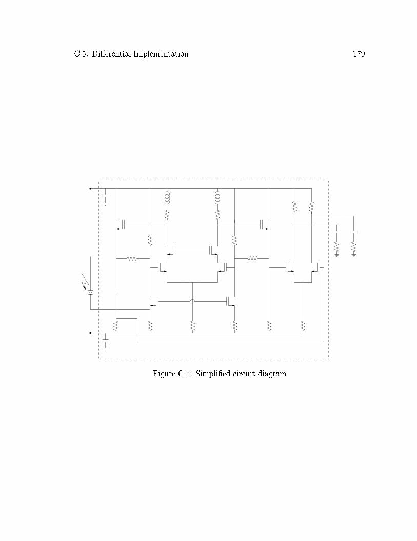
C.5: Di�erential Implementation 179
Figure C.5: Simpli�ed circuit diagram

180 Appendix C: Bandwidth Extension using Optimized On-Chip Inductors
used throughout the preampli�er, resulting in a substantial power saving, while re-
taining the same bandwidth and improving sensitivity. Alternatively, the reduced
capacitance would allow the design of preampli�ers with increased bandwidth sup-
porting faster baud rates.
C.6 Noise Considerations
The sensitivity of the preampli�er is usually expressed as the equivalent integrated
input-referred current noise density. Much literature exists concerning the minimum
noise conditions for conventional optical preampli�ers [43, 48]. Some studies have
also investigated how inductors can increase the sensitivity of optical preampli�ers
implemented in GaAs [44].
The noise performance of the common-gate (CG) input stage followed by the
common-source (CG) transimpedance stage has been studied in GaAs HBT and
BiCMOS processes [49]. Although a simulation involving a single-ended CMOS ver-
sion was reported, it ignored the e�ects of the source and drain junction capacitances
and did not consider the impact of short-channel e�ects on small signal behavior and
noise [50].
Junction capacitances in submicron CMOS processes are comparable to the gate
capacitances and therefore signi�cantly in uence both noise behavior and band-
width. A rigorous analysis that includes the impact of the junction capacitances
and short-channel behavior yields two conditions for a noise optimum. First, the
saturation mode gate capacitance of the common-source stage must equal the satu-
ration mode drain capacitance of the common-gate stage so that Cgs;CS + Cgd;CS =
Cgd;CG+Cdb;CG. Second, the saturation mode input capacitance of the common-gate
stage (which is the gate-source capacitance, Cgs;CG, plus the source-substrate capac-
itance Csb;CG) must equal �Cext, where � � 0:8�1. The factor � is a function of !T,
the coe�cients of channel thermal noise ( ), and the ratios of junction capacitance
to gate capacitance, all of which are bias dependent. For a typical CMOS device in
saturation, (Cgs + Csb) is around 3-4 times as big as (Cgd + Cdb) and therefore the
common-source stage can now be sized smaller, allowing a corresponding increase

C.7: Layout and Experimental Details 181
in the feedback resistance and a dramatic decrease in power consumption, while re-
taining the same device fT. The bu�er stage that follows the common-source stage
can also be sized smaller, as can the width of all the interconnects, resulting in a
smaller die area. The transconductance of the common-gate stage only needs to
be large enough to ensure that the input pole is non-dominant, enabling the power
consumption of the �rst stage to be small.
The introduction of the common-gate stage introduces three new noise sources:
the thermal noise of the source resistor, the thermal noise of the drain resistor, and
the thermal channel noise of the common-gate transistor. Of these terms, careful
design ensures that the resistors are made large enough so as not to signi�cantly
a�ect the noise performance. The thermal channel noises of the common-gate and
common-source devices are re ected at the input by equivalent current noise spec-
tral densities proportional to the square of the frequency. When integrated over
frequency, these terms dominate, a behavior typical of short-channel CMOS pro-
cesses, where carrier velocity saturation conditions cause thermal channel noise to
increase due to excess noise stemming from hot electron e�ects [35, 51]. Balanc-
ing that degradation is the higher fTdelivered by the continuing reduction in gate
length, thereby improving noise performance. However, carrier velocity saturation
causes the small signal transconductance (and fT) to be smaller than that predicted
by long channel (square-law) approximations.
C.7 Layout and Experimental Details
As shown in the die photo (�gure C.6), the chip area is dominated by the passive
components, which is typical of RFICs. However, the two inductors combined occupy
less than 15% of the total area, thanks to the optimized shunt-peaking technique
described in the earlier sections. A patterned ground shield is used beneath the
inductors to reduce substrate coupling [52]. Di�erential symmetry and cross quad
layout are used to ensure maximum matching, thereby reducing common-mode noise
and systematic o�set. On chip capacitance of 16pF is used to provide supply de-
coupling. Several substrate contacts, placed around the transistors, minimize source

182 Appendix C: Bandwidth Extension using Optimized On-Chip Inductors
Figure C.6: Preampli�er die photo

C.7: Layout and Experimental Details 183
Figure C.7: Inductor test structure
inductance. The oor plan keeps the sensitive input bond pads as far away from the
other pads as possible.
Figure C.7 shows the test structure of the spiral inductor used for shunt-peaking.
The S-parameters of the inductor were measured using coplanar ground-signal-
ground (GSG) probes and an open calibration structure. The inductance and the
one-terminal impedance (which is the relevant measure in our ampli�er) were ex-
tracted from these measurements. As shown in �gure C.8, good agreement between
the prediction of the lumped circuit inductor model and measured data is obtained
for the equivalent one-terminal impedance of the spiral inductor used for shunt-
peaking. In particular, we note that the measured inductance of 20:5nH matches

184 Appendix C: Bandwidth Extension using Optimized On-Chip Inductors
real(ZL) measuredreal(ZL) predictedimag(ZL) measuredimag(ZL) predicted
00 0:5 1:0 1:5 2:0 2:5 3:0
200
400
600
800
1000
Frequency (GHz)
Impedance()
Figure C.8: Simulated and measured one-terminal impedance of the spiral inductor
used for shunt-peaking: dout = 180�m, n = 11:75 turns, w = 3:2�m, s = 2:1�m andt = 2:1�m with L = 20nH

C.7: Layout and Experimental Details 185
0 0:2 0:4 0:6 0:8 1:0 1:2
1200
1400
1600
1800
800
1000
CPD = 100fF
CPD = 300fF
CPD = 500fF
CPD = 700fF
Frequency (GHz)
Transimpedance()
Figure C.9: Simulated transimpedance vs. frequency
the 20:3nH value predicted by our simple inductance expressions to within a 1%
error.
Figure C.9 shows the preampli�er's simulated transimpedance versus frequency
for photodiode capacitances varying from 100fF to 700fF. As can be seen, the
3dB bandwidth is around 1:2GHz and is only weakly dependent on the photodiode
capacitance. Maximum gain peaking is 1dB. These simulations are run with the
output driving a 50 resistance and 1pF capacitance.
Figure C.10 illustrates the preampli�er's simulated equivalent input referred cur-
rent noise spectral density for a photodiode capacitance of 600fF. The coe�cient of

186 Appendix C: Bandwidth Extension using Optimized On-Chip Inductors
00 0:5 1:0 1:5 2:0
10
20
30
40
= 2=3
= 4=3
= 2
Frequency (GHz)
pA=
pHz
Figure C.10: Input referred current noise density
channel thermal noise ( ) is varied from 2=3, the long-channel value, to 2, to dis-
cern the degradation in sensitivity due to excess noise in short channel devices. The
worst case value of 2 predicts an input referred current noise of 0:6�A, a signi�cant
degradation from the 0:4�A predicted by long-channel estimates.
Figure C.11(a) and Figure C.11(b) display the measured single-sided output eye
diagrams for operation at 2.1 and 1.6 Gbaud respectively. An open eye is obtained for
single-sided output voltages extending from 4mV to 500mV. Table C.1 summarizes
the performance of the prototype chip.

C.8: Summary 187
mV
ns
0
40
120
80
�40
�120�80
6:0 6:1 6:2 6:3 6:4 6:5 6:6
(a)
mV
ns
0
5
10
15
20
�5�10�15�20�25
25
6:2 6:4 6:6 6:8 7:0 7:2
(b)
Figure C.11: Measured output eye diagrams (a) at 2.1Gbaud, and (b) at 1.6Gbaud.

188 Appendix C: Bandwidth Extension using Optimized On-Chip Inductors
Transimpedance (small-signal) 1600 (di�erential)
800 (single-ended)
Bandwidth (3dB) 1:2GHz
Max. photodiode capacitance 0:6pF
Max. input current 1:0mA
Simulated input noise current 0:6�A
Max. output voltage swing 1:0Vpp (di�erential)
(50 load at each output) 0:5Vpp (single-ended)
Power consumption 115mW (core)
110mW (50 driver)
Die area 0:6mm2
Technology 0:5�m CMOS
Table C.1: Performance summary
C.8 Summary
This appendix presented an area and power e�cient technique for boosting the band-
width of broadband systems using optimized on-chip inductors as shunt-peaking ele-
ments. These bandwidth extension and circuit optimization techniques were applied
in the implementation of a 2:125Gbaud, 1:6k di�erential transimpedance pream-
pli�er with an equivalent input current noise of 0:6�A. The chip has a die area
of 0:6mm2, of which less than 15% is consumed by the two inductors. Designed
in a triple metal, single poly, 0.5�m CMOS process, this chip was intended as a
test vehicle to demonstrate how on-chip bandwidth extension techniques can push
the limits of low-cost CMOS processes. To the best of our knowledge, this chip is
the �rst CMOS implementation that uses planar spiral inductors as shunt-peaking
elements.

Bibliography
[1] J. J. Zhou and D. J. Allstot, \Monolithic transformers and their application
in a di�erential CMOS RF low-noise ampli�er," IEEE Journal of Solid-State
Circuits, vol. 33, no. 12, pp. 2020{2027, Dec. 1998.
[2] D. K. Shae�er et al., \A 115mW, 0.5�m CMOS GPS receiver with widedynamic-range active �lters," IEEE Journal of Solid-State Circuits, vol. 33,no. 12, Dec. 1998.
[3] A. R. Shahani et al., \Low power dividerless frequency synthesis using aperture
phase detection," IEEE Journal of Solid-State Circuits, vol. 33, no. 12, Dec.
1998.
[4] J. Craninckx and M. Steyeart, \A 1.8-GHz low-phase-noise CMOS VCO using
optimized hollow spiral inductors," IEEE Journal of Solid-State Circuits, vol.
32, no. 5, pp. 736{744, May 1997.
[5] N. M. Nguyen and R. G. Meyer, \Si IC-compatible inductors and LC passive
�lters," IEEE Journal of Solid-State Circuits, vol. 25, no. 4, pp. 1028{1031,
August 1990.
[6] J. R. Long and M. A. Copeland, \The modeling, characterization, and design of
monolithic inductors for silicon RF IC's," IEEE Journal of Solid-State Circuits,
vol. 32, no. 3, pp. 357{369, March 1997.
[7] C. P. Yue, C. Ryu, J. Lau, T. H. Lee, and S. S. Wong, \A physical model for
planar spiral inductors on silicon," in Proceedings IEEE IEDM'96, 1996.
[8] J. Crols, P. Kinget, J. Craninckx, and M. Steyeart, \An analytical model
of planar inductors on lowly doped silicon substrates for analog design up to3GHz," in Symposium on VLSI Circuits, Digest of Technical Papers, 1996, pp.
28{29.
189

190 Bibliography
[9] J. N. Burghartz, K. A. Jenkins, and M. Soyuer, \Multilevel-spiral inductors
using VLSI interconnect technology," IEEE Electron device letters, vol. 17, no.
9, pp. 428{430, September 1996.
[10] R. B. Merrill, T. W. Lee, H. You, R. Rasmussen, and L. A. Moberly, \Op-
timization of high Q integrated inductors for multi-level metal CMOS," in
Proceedings IEEE IEDM'95, 1995, pp. 38.7.1{38.7.4.
[11] A. M. Niknejad and R. G. Meyer, \Analysis and optimization of monolithic
inductors and transformers for RF IC's," IEEE Journal of Solid-State Circuits,
vol. 33, pp. 1470{1481, oct 1998.
[12] C. P. Yue and S. S. Wong, \Design strategy of on-chip inductors for highlyintegrated RF systems," in Design Automation Conference, session 54.1, June
1999, pp. 982{987.
[13] E. M. Freeman, \MagNet 5 user guide -Using the MagNet version 5 packagefrom Infolytica," Infolytica, 1993.
[14] EM-Sonnet Software User's Manuals, Sonnet Software Inc., 2.3 edition, 1992.
[15] H. M. Greenhouse, \Design of planar rectangular microelectronic inductors,"IEEE Transactions on parts, hybrids, and packaging, vol. PHP-10, no. 2, pp.
101{109, June 1974.
[16] K. B. Ashby, I. A. Koullias, W. C. Finley, J. J. Bastek, and S. Moinian, \High Qinductors for wireless applications in a complementary silicon bipolar process,"IEEE Journal of Solid-State Circuits, vol. 31, no. 1, pp. 4{9, January 1996.
[17] J. O. Voorman, Continuous-time analog integrated �lters, IEEE Press, 1993.
[18] H. G. Dill, \Designing inductors for thin-�lm applications," Electronic Design,
vol. 12, no. 4, pp. 52{59, 1964.
[19] H. E. Bryan, \Printed inductors and capacitors," Tele-tech and electronic
industries, December 1955.
[20] H. Ronkainen, H. Kattelus, E. Tarvainen, T. Riihisaari, M. Anderson, andP. Kuivalainen, \IC compatible planar inductors on silicon," IEE Proceedings
Circuits Devices Systems, vol. 144, no. 1, pp. 29{35, February 1997.
[21] F. E. Neumann, \Die mathematischen gesetze der inducirten elektrischen
strome (The mathematical laws of induced electrical currents)-1845," in Franz
Neumanns Gesammelte Werke (Franz Neumann's Complete Works), vol. 3.
Druck Und Verlag Von B.G.Teubner, 1912.

Bibliography 191
[22] E. B. Rosa, \The self and mutual inductances of linear conductors," Bull.
Bureau of Standards, vol. 4, no. 2, pp. 301{344, 1908.
[23] J. C. Maxwell, A Treatise on Electricity and Magne, Dover, 3 edition, 1967.
[24] E. B. Rosa and F. W. Grover, \Formulas and tables for the calculation of
mutual and self-inductance," Bull. Bureau of Standards, vol. 8, no. 2, pp. 1{
237, 1912.
[25] H. Nagaoka, \The inductance coe�cients of solenoids," Journal of the College
of Science, Tokyo, vol. 27, August 1909.
[26] H. A. Wheeler, \Simple inductance formulas for radio coils," Proceedings of
the IRE, vol. 16, no. 10, pp. 1398{1400, October 1928.
[27] S. Boyd and L. Vandenberghe, \Introduction to convex op-
timization with engineering applications," Course Notes, 1999,http://www.stanford.edu/class/ee364/.
[28] M. Hershenson, S. P. Boyd, and T. H. Lee, \GPCAD: A tool for CMOS op-amp synthesis," in Proceedings of the IEEE/ACM International Conference on
Computer Aided Design, San Jose, CA, Nov. 1998, pp. 296{303.
[29] M. Hershenson, S. S. Mohan, S. P. Boyd, and T. H. Lee, \Optimization of in-
ductor circuits via geometric programming," in Design Automation Conference,
session 54.3, June 1999, pp. 994{998.
[30] A. M. Niknejad and R. G. Meyer, \Analysis and optimization of monolithic
inductors and transformers for RF IC's," in Proceedings IEEE CICC'97, 1997,
pp. 16.3.1{16.3.4.
[31] S. S. Mohan, C. P. Yue, M. Hershenson, T. H. Lee, and S. S. Wong, \Modeling
and characterization of on-chip transformers," in Proceedings IEEE IEDM'98,December 1998, pp. 531{534.
[32] P. Basedau and Q. Huang, \A 1 GHz monolithic oscillator in 1�m CMOS," in
Proceedings of the European solid-satte circuits conference, 1994.
[33] D. Eggert, P. Huebler, A. Huerrich, H. Kueck, W. Budde, and M. Vorwerk, \A
SOI-RF-CMOS technology on high resistivity SIMOX substrates for microwaveapplications to 5 GHz," IEEE Transactions on Electron Devices, vol. 44, no.
11, pp. 1981{1989, 1997.

192 Bibliography
[34] T. H. Lee, The Design of CMOS Radio-Frequency Integrated Circuits, Cam-
bridge University Press, 1998.
[35] D. K. Shae�er and Thomas H. Lee, \A 1.5V, 1.5GHz CMOS low-noise ampli-
�er," IEEE Journal of Solid-State Circuits, vol. 32, no. 5, pp. 745{759, May
1997.
[36] D. K. Shae�er, The design and implementation of low-power CMOS radio
receivers, Ph.D. thesis, Stanford University, Dec. 1999.
[37] Ali Hajimiri and Thomas H. Lee, \A general theory of phase noise in electrical
oscillators," IEEE Journal of Solid-State Circuits, vol. 33, no. 2, pp. 179{194,Feb. 1998.
[38] R. J. Du�n, E. L. Peterson, and C. Zener, Geometric Programming | Theory
and Applications, Wiley, 1967.
[39] Y. Nesterov and A. Nemirovsky, Interior-point polynomial methods in convex
programming, vol. 13 of Studies in Applied Mathematics, SIAM, Philadelphia,PA, 1994.
[40] M. Hershenson, CMOS analog circuit design via geometric programming, Ph.D.thesis, Stanford University, Dec. 1999.
[41] M. Hershenson, S. S. Mohan, S. P. Boyd, and T. H. Lee, \Optimization of in-ductor circuits via geometric programming," in Design Automation Conference,
session 54.3, June 1999, pp. 994{998.
[42] M. Hershenson, A. Hajimiri, S. S. Mohan, S. P. Boyd, and T. H. Lee, \De-
sign and optimization of LC oscillators," in Proceedings of the IEEE/ACM
International Conference on Computer Aided Design, San Jose, CA, Nov. 1999.
[43] R. G. Smith and S. D. Personik, \Receiver design for optical communication
systems," in Topics in Applied Physics : Semiconductor Devices for Optical
Communication, vol. 39, pp. 89{160. Springer-Verlag, Berlin, Germany, second
edition, 1982.
[44] Norman Scheinberg, Robert J. Bayruns, and Timothy M. Laverick, \Monolithic
GaAs transimpedance ampli�ers for �ber-optic receivers," IEEE Journal of
Solid-State Circuits, vol. 26, no. 12, pp. 1834{1839, Dec. 1991.
[45] S. S. Mohan and T. H. Lee, \A 2:125Gbaud 1:6k! transimpedance pream-pli�er in 0:5�m CMOS," in Custom Integrated Circuits Conference, Digest of
Technical Papers, May 1999.

C.8: Summary 193
[46] S. S. Mohan, M. Hershenson, S. P. Boyd, and T. H. Lee, \Bandwidth exten-
sion in CMOS with optimized on-chip inductors," IEEE Journal of Solid-State
Circuits, vol. 35, no. 3, Mar. 2000.
[47] Z. Lao et al., \25Gb/s AGC ampli�er, 22 GHz transimpedance ampli�er and
27.7GHz limiting ampli�er ICs using AlGaAs/GaAs-HEMTs," in ISSCC Digest
of Technical Papers, 1997, vol. 40, pp. 356{357.
[48] A. A. Abidi, \On the choice of optimum FET size in wide-band transimpedance
ampli�ers," Journal of Lightwave Technology, vol. 6, no. 1, pp. 64{66, Jan. 1988.
[49] T. Vanisri and C. Toumazou, \Integrated high frequency low-noise current-
mode optical transimpedance preampli�ers: Theory and practice," IEEE Jour-
nal of Solid-State Circuits, vol. 30, no. 6, pp. 677{685, June 1995.
[50] C. Toumazou and S. M. Park, \Wideband low noise CMOS transimpedance
ampli�ers for gigahertz operation," Electronics Letters, vol. 32, no. 13, pp.1194{1196, June 1996.
[51] A. A. Abidi, \High-frequency noise measurements on FET's with small dimen-
sions," IEEE Transactions on Electron Devices, vol. 33, no. 11, pp. 1801{1805,1986.
[52] C. Patrick Yue and S. Simon Wong, \On-chip spiral inductors with patternedground shields for Si-based RF IC's," in 1997 Symposium on VLSI Circuits
Digest of Technical Papers, 1997, pp. 85{86.


![[Lab mo] the hub vienna start up lab](https://img.dokumen.tips/doc/110x75/5558a3d4d8b42a2a738b4f8a/lab-mo-the-hub-vienna-start-up-lab.jpg)


![The Green Lab - [04-A] Lab environment and tools](https://img.dokumen.tips/doc/110x75/58a27fce1a28ab891a8b5861/the-green-lab-04-a-lab-environment-and-tools.jpg)

