Embed Size (px)
DESCRIPTION
The Power Electronics Handbook.
Citation preview


POWERELECTRONICS
T H E
H A N D B O O K
© 2002 by CRC Press LLC

I n d u s t r i a l E l e c t r o n i c s S e r i e sSeries Editor
J. David Irwin, Auburn University
Titles included in the series
Supervised and Unsupervised Pattern Recognition:Feature Extraction and Computational Intelligence
Evangelia Micheli-Tzanakou, Rutgers University
Switched Reluctance Motor Drives: Modeling,Simulation, Analysis, Design, and Applications
R. Krishnan, Virginia Tech
The Power Electronics HandbookTimothy L. Skvarenina, Purdue University
The Handbook of Applied Computational IntelligenceMary Lou Padgett, Auburn University
Nicolaos B. Karayiannis, University of HoustonLofti A. Zadeh, University of California, Berkeley
The Handbook of Applied NeurocontrolsMary Lou Padgett, Auburn University
Charles C. Jorgensen, NASA Ames Research CenterPaul Werbos, National Science Foundation
© 2002 by CRC Press LLC

T H E
CRC PR ESSBoca Raton London New York Washington, D.C.
POWERELECTRONICS
Edited by
TIMOTHY L. SKVARENINAPurdue University
West Lafayette, Indiana
Industrial Electronics Series
H A N D B O O K

This book contains information obtained from authentic and highly regarded sources. Reprinted material is quoted withpermission, and sources are indicated. A wide variety of references are listed. Reasonable efforts have been made to publishreliable data and information, but the authors and the publisher cannot assume responsibility for the validity of all materialsor for the consequences of their use.
Neither this book nor any part may be reproduced or transmitted in any form or by any means, electronic or mechanical,including photocopying, microfilming, and recording, or by any information storage or retrieval system, without priorpermission in writing from the publisher.
All rights reserved. Authorization to photocopy items for internal or personal use, or the personal or internal use of specificclients, may be granted by CRC Press LLC, provided that $1.50 per page photocopied is paid directly to Copyright ClearanceCenter, 222 Rosewood Drive, Danvers, MA 01923 USA The fee code for users of the Transactional Reporting Service isISBN 0-8493-7336-0/02/$0.00+$1.50. The fee is subject to change without notice. For organizations that have been granteda photocopy license by the CCC, a separate system of payment has been arranged.
The consent of CRC Press LLC does not extend to copying for general distribution, for promotion, for creating new works,or for resale. Specific permission must be obtained in writing from CRC Press LLC for such copying.
Direct all inquiries to CRC Press LLC, 2000 N.W. Corporate Blvd., Boca Raton, Florida 33431.
Trademark Notice: Product or corporate names may be trademarks or registered trademarks, and are used only foridentification and explanation, without intent to infringe.
Visit the CRC Press Web site at www.crcpress.com
© 2002 by CRC Press LLC
No claim to original U.S. Government worksInternational Standard Book Number 0-8493-7336-0
Library of Congress Card Number 2001043047Printed in the United States of America 1 2 3 4 5 6 7 8 9 0
Printed on acid-free paper
Library of Congress Cataloging-in-Publication Data
The power electronics handbook / edited by Timothy L. Skvarenina.p. cm. — (Industrial electronics series)
Includes bibliographical references and index.ISBN 0-8493-7336-0 (alk. paper)1. Power electronics. I. Skvarenina, Timothy L. II. Series.
TK7881.15 .P673 2001621.31¢7—dc21 2001043047

Preface
Introduction
The control of electric power with power electronic devices has become increasingly important overthe last 20 years. Whole new classes of motors have been enabled by power electronics, and thefuture offers the possibility of more effective control of the electric power grid using power elec-tronics. The Power Electronics Handbook is intended to provide a reference that is both concise anduseful for individuals, ranging from students in engineering to experienced, practicing professionals.The Handbook covers the very wide range of topics that comprise the subject of power electronicsblending many of the traditional topics with the new and innovative technologies that are at theleading edge of advances being made in this subject. Emphasis has been placed on the practicalapplication of the technologies discussed to enhance the value of the book to the reader and toenable a clearer understanding of the material. The presentations are deliberately tutorial in nature,and examples of the practical use of the technology described have been included.
The contributors to this Handbook span the globe and include some of the leading authoritiesin their areas of expertise. They are from industry, government, and academia. All of them have beenchosen because of their intimate knowledge of their subjects as well as their ability to present themin an easily understandable manner.
Organization
The book is organized into three parts. Part I presents an overview of the semiconductor devicesthat are used, or projected to be used, in power electronic devices. Part II explains the operation ofcircuits used in power electronic devices, and Part III describes a number of applications for powerelectronics, including motor drives, utility applications, and electric vehicles.
The Power Electronics Handbook is designed to provide both the young engineer and the experi-enced professional with answers to questions involving the wide spectrum of power electronicstechnology covered in this book. The hope is that the topical coverage, as well as the numerousavenues to its access, will effectively satisfy the reader’s needs.
© 2002 by CRC Press LLC

Acknowledgments
First and foremost, I wish to thank the authors of the individual sections and the editorial advisorsfor their assistance. Obviously, this handbook would not be possible without them. I would like tothank all the people who were involved in the preparation of this handbook at CRC Press, especiallyNora Konopka and Christine Andreasen for their guidance and patience. Finally, my deepest appre-ciation goes to my wife Carol who graciously allows me to pursue activities such as this despite thetime involved.
© 2002 by CRC Press LLC
The Editor
Timothy L. Skvarenina received his B.S.E.E. and M.S.E.E. degrees from the Illinois Institute of Tech-nology in 1969 and 1970, respectively, and his Ph.D. in electrical engineering from Purdue Universityin 1979. In 1970, he entered active duty with the U.S. Air Force, where he served 21 years, retiringas a lieutenant colonel in 1991. During his Air Force career, he spent 6 years designing, constructing,and inspecting electric power distribution projects for a variety of facilities. He also was assigned tothe faculty of the Air Force Institute of Technology (AFIT) for 3 years, where he taught andresearched conventional power systems and pulsed-power systems, including railguns, high-powerswitches, and magnetocumulative generators. Dr. Skvarenina received the Air Force MeritoriousService Medal for his contributions to the AFIT curriculum in 1984. He also spent 4 years with theStrategic Defense Initiative Office (SDIO), where he conducted and directed large-scale systemsanalysis studies. He received the Department of Defense Superior Service Medal in 1991 for hiscontributions to SDIO.
In 1991, Dr. Skvarenina joined the faculty of the School of Technology at Purdue University, wherehe currently teaches undergraduate courses in electrical machines and power systems, as well as agraduate course in facilities engineering. He is a senior member of the IEEE; a member of theAmerican Society for Engineering Education (ASEE), Tau Beta Pi, and Eta Kappa Nu; and a registeredprofessional engineer in the state of Colorado.
Dr. Skvarenina has been active in both IEEE and ASEE. He has held the offices of secretary, vice-chair, and chair of the Central Indiana chapter of the IEEE Power Engineering Society. At the nationallevel he is a member of the Power Engineering Society Education Committee. He has also beenactive in the IEEE Education Society, serving as an associate editor of the Transactions on Educationand co-program chair for the 1999 and 2003 Frontiers in Education Conferences. For his activityand contributions to the Education Society, he received the IEEE Third Millennium Medal in 2000.
Within ASEE, Dr. Skvarenina has been an active member of the Energy Conversion and Conser-vation Division, serving in a series of offices including division chair. In 1999, he was elected by theASEE membership to the Board of Directors for a 2-year term as Chair, Professional Interest CouncilIII. In June 2000, he was elected by the Board of Directors as Vice-President for Profession InterestCouncils for the year 2000–2001.
Dr. Skvarenina is the principal author of a textbook, Electric Power and Controls , published in2001. He has authored or co-authored more than 25 papers in the areas of power systems, powerelectronics, pulsed-power systems, and engineering education.
© 2002 by CRC Press LLC

Editorial Advisors
Mariesa CrowUniversity of Missouri-Rolla Rolla, Missouri
Farhad NozariBoeing CorporationSeattle, Washington
Scott SudhoffPurdue UniversityWest Lafayette, Indiana
Annette von JouanneOregon State UniversityCorvallis, Oregon
Oleg WasynczukPurdue UniversityWest Lafayette, Indiana
© 2002 by CRC Press LLC

Contributors
Ali AgahSharif University of TechnologyTehran, Iran
Ashish AgrawalUniversity of Alaska FairbanksFairbanks, Alaska
Hirofumi AkagiTokyo Institute of TechnologyTokyo, Japan
Sohail AnwarPennsylvania State UniversityAltoona, Pennsylvania
Rajapandian AyyanarArizona State UniversityTempe, Arizona
Vrej BarkhordarianInternational RectifierEl Segundo, California
Ronald H. BrownMarquette UniversityMilwaukee, Wisconsin
Patrick L. ChapmanUniversity of Illinois
at Urbana-ChampaignUrbana, Illinois
Badrul H. ChowdhuryUniversity of Missouri-RollaRolla, Missouri
Keith CorzineUniversity of Wisconsin-
MilwaukeeMilwaukee, Wisconsin
Dariusz CzarkowskiPolytechnic UniversityBrooklyn, New York
Alexander Domijan, Jr.University of FloridaGainesville, Florida
Mehrdad EhsaniTexas A&M UniversityCollege Station, Texas
Ali Emadi Illinois Institute of TechnologyChicago, Illinois
Ali Feliachi West Virginia UniversityMorgantown, West Virginia
Wayne GalliSouthwest Power PoolLittle Rock, Arkansas
Michael GiesselmannTexas Tech UniversityLubbock, Texas
Tilak GopalarathnamTexas A&M UniversityCollege Station, Texas
Sam GuccioneEastern Illinois UniversityCharleston, Illinois
Sándor HalászBudapest University
of Technology and Economics
Budapest, Hungary
Azra Hasanovic West Virginia UniversityMorgantown, West Virginia
John HecklesmillerBest Power Technology, Inc.Nededah, Wisconsin
Alex Q. HuangVirginia Polytechnic Institute
and State UniversityBlacksburg, Virginia
Iqbal HusainThe University of AkronAkron, Ohio
Amit Kumar JainUniversity of MinnesotaMinneapolis, Minnesota
Attila KarpatiBudapest University
of Technology and Economics
Budapest, Hungary
© 2002 by CRC Press LLC

Philip T. KreinUniversity of Illinois
at Urbana-ChampaignUrbana, Illinois
Dave LaydenBest Power Technology, Inc.Nededah, Wisconsin
Daniel LogueUniversity of Illinois
at Urbana-ChampaignUrbana, Illinois
Javad MahdaviSharif University
of TechnologyTehran, Iran
Paolo MattavelliUniversity of PadovaPadova, Italy
Roger MessengerFlorida Atlantic UniversityBoca Raton, Florida
István NagyBudapest University
of Technology and Economics
Budapest, Hungary
Tahmid Ur RahmanTexas A&M UniversityCollege Station, Texas
Kaushik RajashekaraDelphi Automotive SystemsKokomo, Indiana
Michael E. RoppSouth Dakota State UniversityBrookings, South Dakota
Hossein SalehfarUniversity of North DakotaGrand Forks, North Dakota
Bipin SatavalekarUniversity of Alaska FairbanksFairbanks, Alaska
Karl Schoder West Virginia UniversityMorgantown, West Virginia
Daniel Jeffrey ShorttCedarville UniversityCedarville, Ohio
Timothy L. SkvareninaPurdue UniversityWest Lafayette, Indiana
Zhidong SongUniversity of FloridaGainesville, Florida
Giorgio SpiazziUniversity of PadovaPadova, Italy
Ana StankovicCleveland State UniversityCleveland, Ohio
Ralph StausPennsylvania State UniversityReading, Pennsylvania
Laura SteffekBest Power Technology, Inc.Nededah, Wisconsin
Roman StemprokUniversity of North TexasDenton, Texas
Mahesh M. SwamyYaskawa Electric AmericaWaukegan, Illinois
Hamid A. ToliyatTexas A&M UniversityCollege Station, Texas
Eric WaltersP. C. Krause and AssociatesWest Lafayette, Indiana
Oleg WasynczukPurdue UniversityWest Lafayette, Indiana
Richard W. WiesUniversity of Alaska
FairbanksFairbanks, Alaska
Brian YoungBest Power Technology, Inc.Nededah, Wisconsin
© 2002 by CRC Press LLC

Contents
PART I Power Electronic Devices
1 Power Electronics1.1 Overview Kaushik Rajashekara1.2 Diodes Sohail Anwar1.3 Schottky Diodes Sohail Anwar1.4 Thyristors Sohail Anwar1.5 Power Bipolar Junction Transistors Sohail Anwar1.6 MOSFETs Vrej Barkhordarian1.7 General Power Semiconductor Switch Requirements Alex Q. Huang1.8 Gate Turn-Off Thyristors Alex Q. Huang1.9 Insulated Gate Bipolar Transistors Alex Q. Huang1.10 Gate-Commutated Thyristors and Other Hard-Driven GTOs Alex Q. Huang1.11 Comparison Testing of Switches Alex Q. Huang
PART II Power Electronic Circuits and Controls
2 DC-DC Converters2.1 Overview Richard Wies, Bipin Satavalekar, and Ashish Agrawal2.2 Choppers Javad Mahdavi, Ali Agah, and Ali Emadi2.3 Buck Converters Richard Wies, Bipin Satavalekar, and Ashish Agrawal2.4 Boost Converters Richard Wies, Bipin Satavalekar, and Ashish Agrawal2.5 Cúk Converter Richard Wies, Bipin Satavalekar, and Ashish Agrawal2.6 Buck–Boost Converters Daniel Jeffrey Shortt
3 AC-AC Conversion Sándor Halász3.1 Introduction3.2 Cycloconverters3.3 Matrix Converters
4 Rectifiers4.1 Uncontrolled Single-Phase Rectifiers Sam Guccione4.2 Uncontrolled and Controlled Rectifiers Mahesh M. Swamy4.3 Three-Phase Pulse-Width-Modulated Boost-Type Rectifiers Ana Stankovic
© 2002 by CRC Press LLC

5 Inverters5.1 Overview Michael Giesselmann5.2 DC-AC Conversion Attila Karpati5.3 Resonant Converters István Nagy5.4 Series-Resonant Inverters Dariusz Czarkowski5.5 Resonant DC-Link Inverters Michael B. Ropp5.6 Auxiliary Resonant Commutated Pole Inverters
Eric Walters and Oleg Wasynczuk
6 Multilevel Converters Keith Corzine6.1 Introduction6.2 Multilevel Voltage Source Modulation6.3 Fundamental Multilevel Converter Topologies6.4 Cascaded Multilevel Converter Topologies6.5 Multilevel Converter Laboratory Examples6.6 Conclusion
7 Modulation Strategies7.1 Introduction Michael Giesselmann7.2 Six-Step Modulation Michael Giesselmann7.3 Pulse Width Modulation Michael Giesselmann7.4 Third Harmonic Injection for Voltage Boost of SPWM Signals
Michael Giesselmann7.5 Generation of PWM Signals Using Microcontrollers and DSPs
Michael Giesselmann7.6 Voltage-Source-Based Current Regulation Michael Giesselmann7.7 Hysteresis Feedback Control Hossein Salehfar7.8 Space-Vector Pulse Width Modulation
Hamid A. Toliyat and Tahmid Ur Rahman
8 Sliding-Mode Control of Switched-Mode Power SuppliesGiorgio Spiazzi and Paolo Mattavelli8.1 Introduction8.2 Introduction to Sliding-Mode Control8.3 Basics of Sliding-Mode Theory8.4 Application of Sliding-Mode Control to DC-DC Converters—Basic Principle8.5 Sliding-Mode Control of Buck DC-DC Converters8.6 Extension to Boost and Buck–Boost DC-DC Converters8.7 Extension to Cúk and SEPIC DC-DC Converters8.8 General-Purpose Sliding-Mode Control Implementation8.9 Conclusions
© 2002 by CRC Press LLC

Part III Applications and Systems Considerations
9 DC Motor Drives Ralph Staus9.1 DC Motor Basics9.2 DC Speed Control9.3 DC Drive Basics9.4 Transistor PWM DC Drives9.5 SCR DC Drives
10 AC Machines Controlled as DC Machines(Brushless DC Machines/Electronics) Hamid A. Toliyatand Tilak Gopalarathnam10.1 Introduction10.2 Machine Construction10.3 Motor Characteristics10.4 Power Electronic Converter10.5 Position Sensing10.6 Pulsating Torque Components10.7 Torque-Speed Characteristics10.8 Applications
11 Control of Induction Machine DrivesDaniel Logue and Philip T. Krein11.1 Introduction11.2 Scalar Induction Machine Control11.3 Vector Control of Induction Machines11.4 Summary
12 Permanent-Magnet Synchronous Machine Drives Patrick L. Chapman12.1 Introduction12.2 Construction of PMSM Drive Systems12.3 Simulation and Model12.4 Controlling the PMSM12.5 Advanced Topics in PMSM Drives
13 Switched Reluctance Machines Iqbal Husain13.1 Introduction13.2 SRM Configuration13.3 Basic Principle of Operation 13.4 Design 13.5 Converter Topologies 13.6 Control Strategies 13.7 Sensorless Control 13.8 Applications
© 2002 by CRC Press LLC

14 Step Motor Drives Ronald H. Brown14.1 Introduction14.2 Types and Operation of Step Motors14.3 Step Motor Models14.4 Control of Step Motors
15 Servo Drives Sándor Halász15.1 DC Drives15.2 Induction Motor Drives
16 Uninterruptible Power Supplies Laura Steffek, John Hacklesmiller,Dave Layden, and Brian Young16.1 UPS Functions16.2 Static UPS Topologies16.3 Rotary UPSs16.4 Alternate AC and DC Sources
17 Power Quality and Utility Interface Issues17.1 Overview Wayne Galli17.2 Power Quality Considerations Timothy L. Skvarenina 17.3 Passive Harmonic Filters Badrul H. Chowdhury 17.4 Active Filters for Power Conditioning Hirofumi Akagi 17.5 Unity Power Factor Rectification Rajapandian Ayyanar and Amit Kumar Jain
18 Photovoltaic Cells and Systems Roger Messenger18.1 Introduction 18.2 Solar Cell Fundamentals18.3 Utility Interactive PV Applications18.4 Stand-Alone PV Systems
19 Flexible, Reliable, and Intelligent Electrical Energy Delivery SystemsAlexander Domijan, Jr. and Zhidong Song19.1 Introduction 19.2 The Concept of FRIENDS19.3 Development of FRIENDS19.4 The Advanced Power Electronic Technologies within QCCs 19.5 Significance of FRIENDS19.6 Realization of FRIENDS19.7 Conclusions
20 Unified Power Flow ControllersAli Feliachi, Azra Hasanovic, and Karl Schoder20.1 Introduction20.2 Power Flow on a Transmission Line
© 2002 by CRC Press LLC

20.3 UPFC Description and Operation20.4 UPFC Modeling20.5 Control Design20.6 Case Study20.7 ConclusionAcknowledgment
21 More-Electric Vehicles Ali Emadi and Mehrdad Ehsani21.1 Aircraft Ali Emadi and Mehrdad Ehsani21.2 Terrestrial Vehicles Ali Emadi and Mehrdad Ehsani
22 Principles of Magnetics Roman Stemprok22.1 Introduction 22.2 Nature of a Magnetic Field22.3 Electromagnetism22.4 Magnetic Flux Density22.5 Magnetic Circuits22.6 Magnetic Field Intensity22.7 Maxwell’s Equations22.8 Inductance22.9 Practical Considerations
23 Computer Simulation of Power Electronics Michael Giesselmann23.1 Introduction23.2 Code Qualification and Model Validation23.3 Basic Concepts—Simulation of a Buck Converter 23.4 Advanced Techniques—Simulation of a Full-Bridge (H-Bridge) Converter 23.5 Conclusions
© 2002 by CRC Press LLC

IPower Electronic Devices
1 Power Electronics Kaushik Rajashekara, Sohail Anwar, Vrej Barkhordarian,Alex Q. HuangOverview • Diodes • Schottky Diodes • Thyristors • Power Bipolar JunctionTransistors • MOSFETs • General Power Semiconductor Switch Requirements • GateTurn-Off Thyristors • Insulated Gate Bipolar Transistors • Gate-Commutated Thyristorsand Other Hard-Driven GTOs • Comparison Testing of Switches
© 2002 by CRC Press LLC

1Power Electronics
1.1 OverviewThyristor and Triac • Gate Turn-Off Thyristor • Reverse-Conducting Thyristor (RCT) and Asymmetrical Silicon-Controlled Rectifier (ASCR) • Power Transistor • Power MOSFET • Insulated-Gate Bipolar Transistor (IGBT) •MOS-Controlled Thyristor (MCT)
1.2 DiodesCharacteristics • Principal Ratings for Diodes • Rectifier Circuits • Testing a Power Diode • Protection of Power Diodes
1.3 Schottky DiodesCharacteristics • Data Specifications • Testing of Schottky Diodes
1.4 ThyristorsThe Basics of Silicon-Controlled Rectifiers (SCR) •Characteristics • SCR Turn-Off Circuits • SCR Ratings • The DIAC • The Triac • The Silicon-Controlled Switch • The Gate Turn-Off Thyristor • Data Sheet for a Typical Thyristor
1.5 Power Bipolar Junction TransistorsThe Volt-Ampere Characteristics of a BJT • BJT Biasing • BJT Power Losses • BJT Testing • BJT Protection
1.6 MOSFETsStatic Characteristics • Dynamic Characteristics • Applications
1.7 General Power Semiconductor SwitchRequirements
1.8 Gate Turn-Off ThyristorsGTO Forward Conduction • GTO Turn-Off and Forward Blocking • Practical GTO Turn-Off Operation • Dynamic Avalanche • Non-Uniform Turn-Off Process among GTO Cells • Summary
1.9 Insulated Gate Bipolar TransistorsIGBT Structure and Operation
1.10 Gate-Commutated Thyristors and OtherHard-Driven GTOsUnity Gain Turn-Off Operation • Hard-Driven GTOs
1.11 Comparison Testing of SwitchesPulse Tester Used for Characterization • Devices Used for Comparison • Unity Gain Verification • Gate Drive Circuits • Forward Conduction Loss Characterization •Switching Tests • Discussion • Comparison Conclusions
Kaushik RajashekaraDelphi Automotive Systems
Sohail AnwarPennsylvania State University
Vrej BarkhordarianInternational Rectifier
Alex Q. HuangVirginia Polytechnic Institute and State University
© 2002 by CRC Press LLC
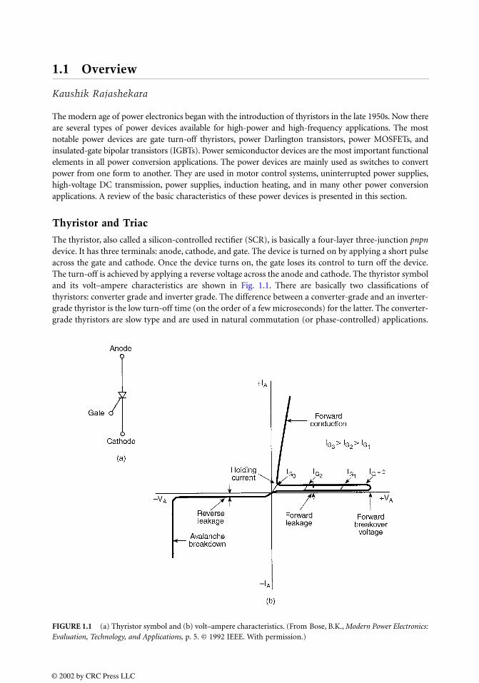
1.1 Overview
Kaushik Rajashekara
The modern age of power electronics began with the introduction of thyristors in the late 1950s. Now thereare several types of power devices available for high-power and high-frequency applications. The mostnotable power devices are gate turn-off thyristors, power Darlington transistors, power MOSFETs, andinsulated-gate bipolar transistors (IGBTs). Power semiconductor devices are the most important functionalelements in all power conversion applications. The power devices are mainly used as switches to convertpower from one form to another. They are used in motor control systems, uninterrupted power supplies,high-voltage DC transmission, power supplies, induction heating, and in many other power conversionapplications. A review of the basic characteristics of these power devices is presented in this section.
Thyristor and Triac
The thyristor, also called a silicon-controlled rectifier (SCR), is basically a four-layer three-junction pnpndevice. It has three terminals: anode, cathode, and gate. The device is turned on by applying a short pulseacross the gate and cathode. Once the device turns on, the gate loses its control to turn off the device.The turn-off is achieved by applying a reverse voltage across the anode and cathode. The thyristor symboland its volt–ampere characteristics are shown in Fig. 1.1. There are basically two classifications ofthyristors: converter grade and inverter grade. The difference between a converter-grade and an inverter-grade thyristor is the low turn-off time (on the order of a few microseconds) for the latter. The converter-grade thyristors are slow type and are used in natural commutation (or phase-controlled) applications.
FIGURE 1.1 (a) Thyristor symbol and (b) volt–ampere characteristics. (From Bose, B.K., Modern Power Electronics:Evaluation, Technology, and Applications, p. 5. © 1992 IEEE. With permission.)
© 2002 by CRC Press LLC

Inverter-grade thyristors are used in forced commutation applications such as DC-DC choppers andDC-AC inverters. The inverter-grade thyristors are turned off by forcing the current to zero using anexternal commutation circuit. This requires additional commutating components, thus resulting inadditional losses in the inverter.
Thyristors are highly rugged devices in terms of transient currents, di/dt, and dv/dt capability. Theforward voltage drop in thyristors is about 1.5 to 2 V, and even at higher currents of the order of 1000 A,it seldom exceeds 3 V. While the forward voltage determines the on-state power loss of the device at anygiven current, the switching power loss becomes a dominating factor affecting the device junctiontemperature at high operating frequencies. Because of this, the maximum switching frequencies possibleusing thyristors are limited in comparison with other power devices considered in this section.
Thyristors have I2t withstand capability and can be protected by fuses. The nonrepetitive surge current
capability for thyristors is about 10 times their rated root mean square (rms) current. They must be protectedby snubber networks for dv/dt and di/dt effects. If the specified dv/dt is exceeded, thyristors may startconducting without applying a gate pulse. In DC-to-AC conversion applications, it is necessary to use anantiparallel diode of similar rating across each main thyristor. Thyristors are available up to 6000 V, 3500 A.
A triac is functionally a pair of converter-grade thyristors connected in antiparallel. The triac symboland volt–ampere characteristics are shown in Fig. 1.2. Because of the integration, the triac has poor reapplieddv/dt, poor gate current sensitivity at turn-on, and longer turn-off time. Triacs are mainly used in phasecontrol applications such as in AC regulators for lighting and fan control and in solid-state AC relays.
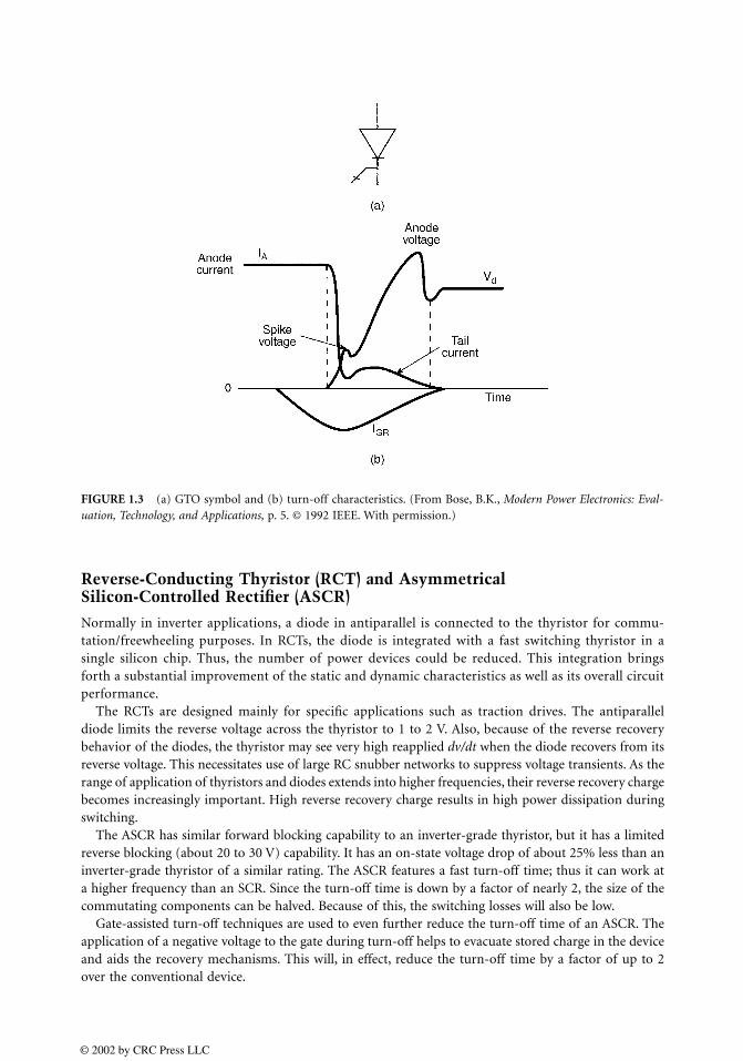
Gate Turn-Off Thyristor
The GTO is a power switching device that can be turned on by a short pulse of gate current and turnedoff by a reverse gate pulse. This reverse gate current amplitude is dependent on the anode current to beturned off. Hence there is no need for an external commutation circuit to turn it off. Because turn-offis provided by bypassing carriers directly to the gate circuit, its turn-off time is short, thus giving it morecapability for high-frequency operation than thyristors. The GTO symbol and turn-off characteristicsare shown in Fig. 1.3.
GTOs have the I2t withstand capability and hence can be protected by semiconductor fuses. For reliable
operation of GTOs, the critical aspects are proper design of the gate turn-off circuit and the snubbercircuit. A GTO has a poor turn-off current gain of the order of 4 to 5. For example, a 2000-A peak currentGTO may require as high as 500 A of reverse gate current. Also, a GTO has the tendency to latch attemperatures above 125°C. GTOs are available up to about 4500 V, 2500 A.
FIGURE 1.2 (a) Triac symbol and (b) volt–ampere characteristics. (From Bose, B.K., Modern Power Electronics:Evaluation, Technology, and Applications, p. 5. © 1992 IEEE. With permission.)
© 2002 by CRC Press LLC
Reverse-Conducting Thyristor (RCT) and AsymmetricalSilicon-Controlled Rectifier (ASCR)
Normally in inverter applications, a diode in antiparallel is connected to the thyristor for commu-tation/freewheeling purposes. In RCTs, the diode is integrated with a fast switching thyristor in asingle silicon chip. Thus, the number of power devices could be reduced. This integration bringsforth a substantial improvement of the static and dynamic characteristics as well as its overall circuitperformance.
The RCTs are designed mainly for specific applications such as traction drives. The antiparalleldiode limits the reverse voltage across the thyristor to 1 to 2 V. Also, because of the reverse recoverybehavior of the diodes, the thyristor may see very high reapplied dv/dt when the diode recovers from itsreverse voltage. This necessitates use of large RC snubber networks to suppress voltage transients. As therange of application of thyristors and diodes extends into higher frequencies, their reverse recovery chargebecomes increasingly important. High reverse recovery charge results in high power dissipation duringswitching.
The ASCR has similar forward blocking capability to an inverter-grade thyristor, but it has a limitedreverse blocking (about 20 to 30 V) capability. It has an on-state voltage drop of about 25% less than aninverter-grade thyristor of a similar rating. The ASCR features a fast turn-off time; thus it can work ata higher frequency than an SCR. Since the turn-off time is down by a factor of nearly 2, the size of thecommutating components can be halved. Because of this, the switching losses will also be low.
Gate-assisted turn-off techniques are used to even further reduce the turn-off time of an ASCR. Theapplication of a negative voltage to the gate during turn-off helps to evacuate stored charge in the deviceand aids the recovery mechanisms. This will, in effect, reduce the turn-off time by a factor of up to 2over the conventional device.
FIGURE 1.3 (a) GTO symbol and (b) turn-off characteristics. (From Bose, B.K., Modern Power Electronics: Eval-uation, Technology, and Applications, p. 5. © 1992 IEEE. With permission.)
© 2002 by CRC Press LLC
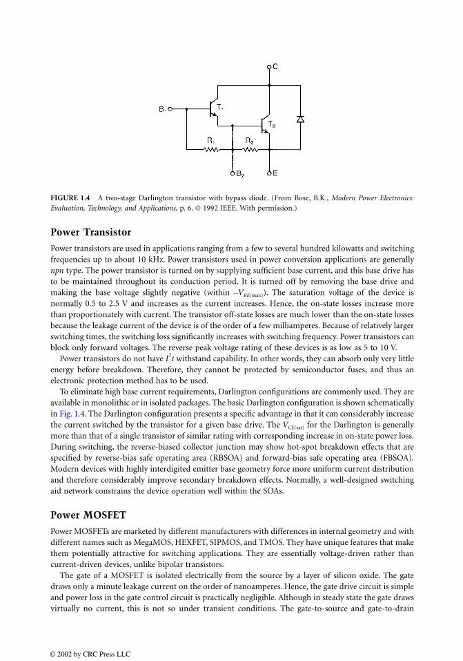
Power Transistor
Power transistors are used in applications ranging from a few to several hundred kilowatts and switchingfrequencies up to about 10 kHz. Power transistors used in power conversion applications are generallynpn type. The power transistor is turned on by supplying sufficient base current, and this base drive hasto be maintained throughout its conduction period. It is turned off by removing the base drive andmaking the base voltage slightly negative (within –VBE(max)). The saturation voltage of the device isnormally 0.5 to 2.5 V and increases as the current increases. Hence, the on-state losses increase morethan proportionately with current. The transistor off-state losses are much lower than the on-state lossesbecause the leakage current of the device is of the order of a few milliamperes. Because of relatively largerswitching times, the switching loss significantly increases with switching frequency. Power transistors canblock only forward voltages. The reverse peak voltage rating of these devices is as low as 5 to 10 V.
Power transistors do not have I2t withstand capability. In other words, they can absorb only very little
energy before breakdown. Therefore, they cannot be protected by semiconductor fuses, and thus anelectronic protection method has to be used.
To eliminate high base current requirements, Darlington configurations are commonly used. They areavailable in monolithic or in isolated packages. The basic Darlington configuration is shown schematicallyin Fig. 1.4. The Darlington configuration presents a specific advantage in that it can considerably increasethe current switched by the transistor for a given base drive. The VCE(sat) for the Darlington is generallymore than that of a single transistor of similar rating with corresponding increase in on-state power loss.During switching, the reverse-biased collector junction may show hot-spot breakdown effects that arespecified by reverse-bias safe operating area (RBSOA) and forward-bias safe operating area (FBSOA).Modern devices with highly interdigited emitter base geometry force more uniform current distributionand therefore considerably improve secondary breakdown effects. Normally, a well-designed switchingaid network constrains the device operation well within the SOAs.
Power MOSFET
Power MOSFETs are marketed by different manufacturers with differences in internal geometry and withdifferent names such as MegaMOS, HEXFET, SIPMOS, and TMOS. They have unique features that makethem potentially attractive for switching applications. They are essentially voltage-driven rather thancurrent-driven devices, unlike bipolar transistors.
The gate of a MOSFET is isolated electrically from the source by a layer of silicon oxide. The gatedraws only a minute leakage current on the order of nanoamperes. Hence, the gate drive circuit is simpleand power loss in the gate control circuit is practically negligible. Although in steady state the gate drawsvirtually no current, this is not so under transient conditions. The gate-to-source and gate-to-drain
FIGURE 1.4 A two-stage Darlington transistor with bypass diode. (From Bose, B.K., Modern Power Electronics:Evaluation, Technology, and Applications, p. 6. © 1992 IEEE. With permission.)
© 2002 by CRC Press LLC
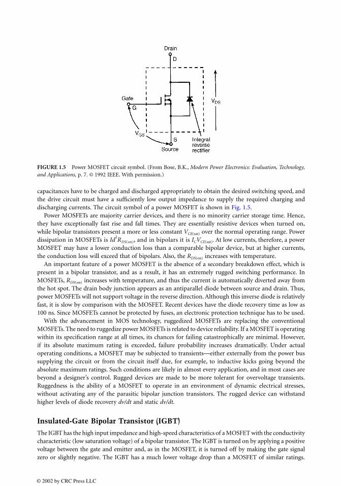
capacitances have to be charged and discharged appropriately to obtain the desired switching speed, andthe drive circuit must have a sufficiently low output impedance to supply the required charging anddischarging currents. The circuit symbol of a power MOSFET is shown in Fig. 1.5.
Power MOSFETs are majority carrier devices, and there is no minority carrier storage time. Hence,they have exceptionally fast rise and fall times. They are essentially resistive devices when turned on,while bipolar transistors present a more or less constant VCE(sat) over the normal operating range. Powerdissipation in MOSFETs is Id
2RDS(on), and in bipolars it is ICVCE(sat). At low currents, therefore, a power
MOSFET may have a lower conduction loss than a comparable bipolar device, but at higher currents,the conduction loss will exceed that of bipolars. Also, the RDS(on) increases with temperature.
An important feature of a power MOSFET is the absence of a secondary breakdown effect, which ispresent in a bipolar transistor, and as a result, it has an extremely rugged switching performance. InMOSFETs, RDS(on) increases with temperature, and thus the current is automatically diverted away fromthe hot spot. The drain body junction appears as an antiparallel diode between source and drain. Thus,power MOSFETs will not support voltage in the reverse direction. Although this inverse diode is relativelyfast, it is slow by comparison with the MOSFET. Recent devices have the diode recovery time as low as100 ns. Since MOSFETs cannot be protected by fuses, an electronic protection technique has to be used.
With the advancement in MOS technology, ruggedized MOSFETs are replacing the conventionalMOSFETs. The need to ruggedize power MOSFETs is related to device reliability. If a MOSFET is operatingwithin its specification range at all times, its chances for failing catastrophically are minimal. However,if its absolute maximum rating is exceeded, failure probability increases dramatically. Under actualoperating conditions, a MOSFET may be subjected to transients—either externally from the power bussupplying the circuit or from the circuit itself due, for example, to inductive kicks going beyond theabsolute maximum ratings. Such conditions are likely in almost every application, and in most cases arebeyond a designer’s control. Rugged devices are made to be more tolerant for overvoltage transients.Ruggedness is the ability of a MOSFET to operate in an environment of dynamic electrical stresses,without activating any of the parasitic bipolar junction transistors. The rugged device can withstandhigher levels of diode recovery dv/dt and static dv/dt.
Insulated-Gate Bipolar Transistor (IGBT)
The IGBT has the high input impedance and high-speed characteristics of a MOSFET with the conductivitycharacteristic (low saturation voltage) of a bipolar transistor. The IGBT is turned on by applying a positivevoltage between the gate and emitter and, as in the MOSFET, it is turned off by making the gate signalzero or slightly negative. The IGBT has a much lower voltage drop than a MOSFET of similar ratings.
FIGURE 1.5 Power MOSFET circuit symbol. (From Bose, B.K., Modern Power Electronics: Evaluation, Technology,and Applications, p. 7. © 1992 IEEE. With permission.)
© 2002 by CRC Press LLC

The structure of an IGBT is more like a thyristor and MOSFET. For a given IGBT, there is a critical value ofcollector current that will cause a large enough voltage drop to activate the thyristor. Hence, the devicemanufacturer specifies the peak allowable collector current that can flow without latch-up occurring. Thereis also a corresponding gate source voltage that permits this current to flow that should not be exceeded.
Like the power MOSFET, the IGBT does not exhibit the secondary breakdown phenomenon commonto bipolar transistors. However, care should be taken not to exceed the maximum power dissipation andspecified maximum junction temperature of the device under all conditions for guaranteed reliableoperation. The on-state voltage of the IGBT is heavily dependent on the gate voltage. To obtain a lowon-state voltage, a sufficiently high gate voltage must be applied.
In general, IGBTs can be classified as punch-through (PT) and nonpunch-through (NPT) structures, asshown in Fig. 1.6. In the PT IGBT, an N
+ buffer layer is normally introduced between the P
+ substrate and
the N− epitaxial layer, so that the whole N
− drift region is depleted when the device is blocking the off-state
voltage, and the electrical field shape inside the N− drift region is close to a rectangular shape. Because a
shorter N− region can be used in the punch-through IGBT, a better trade-off between the forward voltage
drop and turn-off time can be achieved. PT IGBTs are available up to about 1200 V.High-voltage IGBTs are realized through a nonpunch-through process. The devices are built on an N
−
wafer substrate which serves as the N− base drift region. Experimental NPT IGBTs of up to about 4 kV
have been reported in the literature. NPT IGBTs are more robust than PT IGBTs, particularly under shortcircuit conditions. But NPT IGBTs have a higher forward voltage drop than the PT IGBTs.
The PT IGBTs cannot be as easily paralleled as MOSFETs. The factors that inhibit current sharing ofparallel-connected IGBTs are (1) on-state current unbalance, caused by VCE(sat) distribution and maincircuit wiring resistance distribution, and (2) current unbalance at turn-on and turn-off, caused by theswitching time difference of the parallel connected devices and circuit wiring inductance distribution.The NPT IGBTs can be paralleled because of their positive temperature coefficient property.
FIGURE 1.6 (a) Nonpunch-through IGBT, (b) punch-through IGBT, (c) IGBT equivalent circuit.
© 2002 by CRC Press LLC
MOS-Controlled Thyristor (MCT)
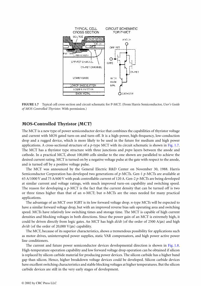
The MCT is a new type of power semiconductor device that combines the capabilities of thyristor voltageand current with MOS gated turn-on and turn-off. It is a high-power, high-frequency, low-conductiondrop and a rugged device, which is more likely to be used in the future for medium and high powerapplications. A cross-sectional structure of a p-type MCT with its circuit schematic is shown in Fig. 1.7.The MCT has a thyristor type structure with three junctions and pnpn layers between the anode andcathode. In a practical MCT, about 100,000 cells similar to the one shown are paralleled to achieve thedesired current rating. MCT is turned on by a negative voltage pulse at the gate with respect to the anode,and is turned off by a positive voltage pulse.
The MCT was announced by the General Electric R&D Center on November 30, 1988. HarrisSemiconductor Corporation has developed two generations of p-MCTs. Gen-1 p-MCTs are available at65 A/1000 V and 75 A/600 V with peak controllable current of 120 A. Gen-2 p-MCTs are being developedat similar current and voltage ratings, with much improved turn-on capability and switching speed.The reason for developing a p-MCT is the fact that the current density that can be turned off is twoor three times higher than that of an n-MCT; but n-MCTs are the ones needed for many practicalapplications.
The advantage of an MCT over IGBT is its low forward voltage drop. n-type MCTs will be expected tohave a similar forward voltage drop, but with an improved reverse bias safe operating area and switchingspeed. MCTs have relatively low switching times and storage time. The MCT is capable of high currentdensities and blocking voltages in both directions. Since the power gain of an MCT is extremely high, itcould be driven directly from logic gates. An MCT has high di/dt (of the order of 2500 A/µs) and highdv/dt (of the order of 20,000 V/µs) capability.
The MCT, because of its superior characteristics, shows a tremendous possibility for applications suchas motor drives, uninterrupted power supplies, static VAR compensators, and high power active powerline conditioners.
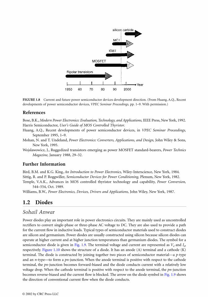
The current and future power semiconductor devices developmental direction is shown in Fig. 1.8.High-temperature operation capability and low forward voltage drop operation can be obtained if siliconis replaced by silicon carbide material for producing power devices. The silicon carbide has a higher bandgap than silicon. Hence, higher breakdown voltage devices could be developed. Silicon carbide deviceshave excellent switching characteristics and stable blocking voltages at higher temperatures. But the siliconcarbide devices are still in the very early stages of development.
FIGURE 1.7 Typical cell cross section and circuit schematic for P-MCT. (From Harris Semiconductor, User’s Guideof MOS Controlled Thyristor. With permission.)
© 2002 by CRC Press LLC
References
Bose, B.K., Modern Power Electronics: Evaluation, Technology, and Applications, IEEE Press, New York, 1992.Harris Semiconductor, User’s Guide of MOS Controlled Thyristor.Huang, A.Q., Recent developments of power semiconductor devices, in VPEC Seminar Proceedings,
September 1995, 1–9.Mohan, N. and T. Undeland, Power Electronics: Converters, Applications, and Design, John Wiley & Sons,
New York, 1995.Wojslawowicz, J., Ruggedized transistors emerging as power MOSFET standard-bearers, Power Technics
Magazine, January 1988, 29–32.
Further Information
Bird, B.M. and K.G. King, An Introduction to Power Electronics, Wiley-Interscience, New York, 1984.Sittig, R. and P. Roggwiller, Semiconductor Devices for Power Conditioning, Plenum, New York, 1982.Temple, V.A.K., Advances in MOS controlled thyristor technology and capability, Power Conversion,
544–554, Oct. 1989.Williams, B.W., Power Electronics, Devices, Drivers and Applications, John Wiley, New York, 1987.
1.2 Diodes
Sohail Anwar
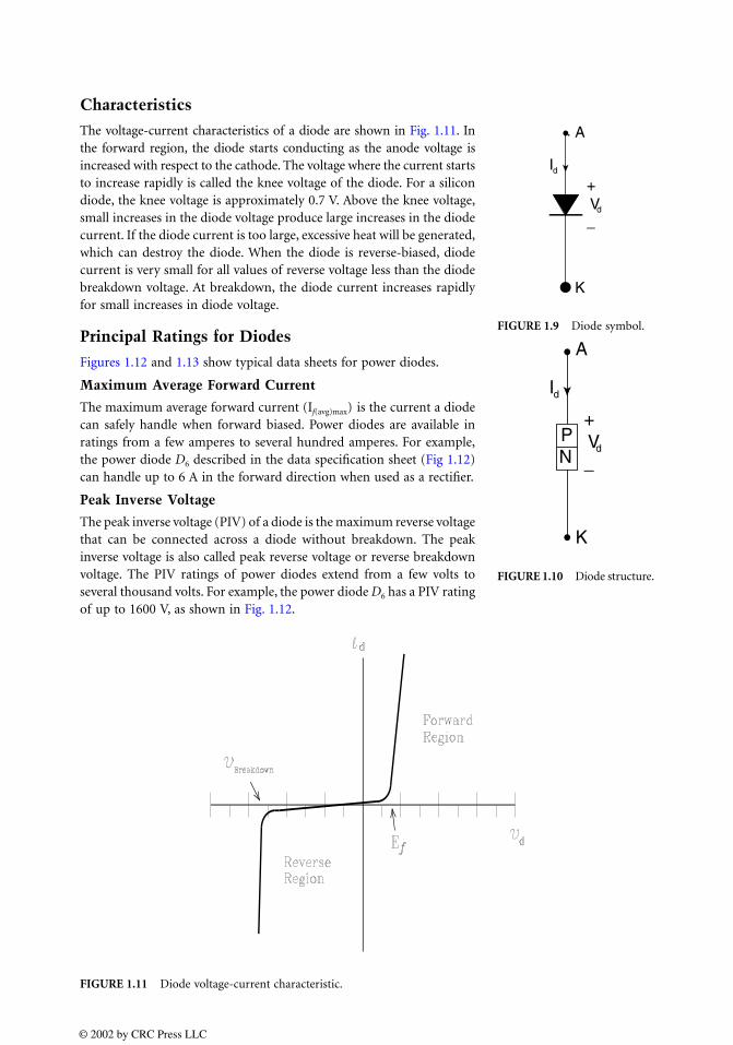
Power diodes play an important role in power electronics circuits. They are mainly used as uncontrolledrectifiers to convert single-phase or three-phase AC voltage to DC. They are also used to provide a pathfor the current flow in inductive loads. Typical types of semiconductor materials used to construct diodesare silicon and germanium. Power diodes are usually constructed using silicon because silicon diodes canoperate at higher current and at higher junction temperatures than germanium diodes. The symbol for asemiconductor diode is given in Fig. 1.9. The terminal voltage and current are represented as Vd and Id,respectively. Figure 1.10 shows the structure of a diode. It has an anode (A) terminal and a cathode (K)terminal. The diode is constructed by joining together two pieces of semiconductor material—a p-typeand an n-type—to form a pn-junction. When the anode terminal is positive with respect to the cathodeterminal, the pn-junction becomes forward-biased and the diode conducts current with a relatively lowvoltage drop. When the cathode terminal is positive with respect to the anode terminal, the pn-junctionbecomes reverse-biased and the current flow is blocked. The arrow on the diode symbol in Fig. 1.9 showsthe direction of conventional current flow when the diode conducts.
FIGURE 1.8 Current and future power semiconductor devices development direction. (From Huang, A.Q., Recentdevelopments of power semiconductor devices, VPEC Seminar Proceedings, pp. 1–9. With permission.)
© 2002 by CRC Press LLC
Characteristics
The voltage-current characteristics of a diode are shown in Fig. 1.11. Inthe forward region, the diode starts conducting as the anode voltage isincreased with respect to the cathode. The voltage where the current startsto increase rapidly is called the knee voltage of the diode. For a silicondiode, the knee voltage is approximately 0.7 V. Above the knee voltage,small increases in the diode voltage produce large increases in the diodecurrent. If the diode current is too large, excessive heat will be generated,which can destroy the diode. When the diode is reverse-biased, diodecurrent is very small for all values of reverse voltage less than the diodebreakdown voltage. At breakdown, the diode current increases rapidlyfor small increases in diode voltage.
Principal Ratings for Diodes
Figures 1.12 and 1.13 show typical data sheets for power diodes.
Maximum Average Forward Current
The maximum average forward current (If(avg)max) is the current a diodecan safely handle when forward biased. Power diodes are available inratings from a few amperes to several hundred amperes. For example,the power diode D6 described in the data specification sheet (Fig 1.12)can handle up to 6 A in the forward direction when used as a rectifier.
Peak Inverse Voltage
The peak inverse voltage (PIV) of a diode is the maximum reverse voltagethat can be connected across a diode without breakdown. The peakinverse voltage is also called peak reverse voltage or reverse breakdownvoltage. The PIV ratings of power diodes extend from a few volts toseveral thousand volts. For example, the power diode D6 has a PIV ratingof up to 1600 V, as shown in Fig. 1.12.
FIGURE 1.11 Diode voltage-current characteristic.
FIGURE 1.9 Diode symbol.
Id
Vd
+
_
A
K
FIGURE 1.10 Diode structure.
Id
Vd
+
_
A
K
PN
© 2002 by CRC Press LLC
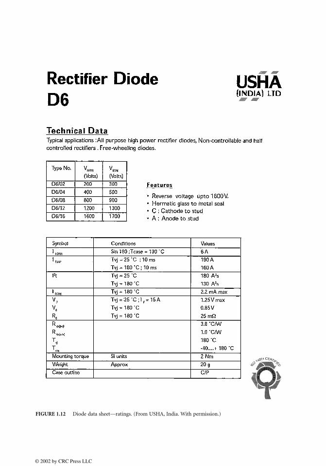
FIGURE 1.12 Diode data sheet—ratings. (From USHA, India. With permission.)
© 2002 by CRC Press LLC
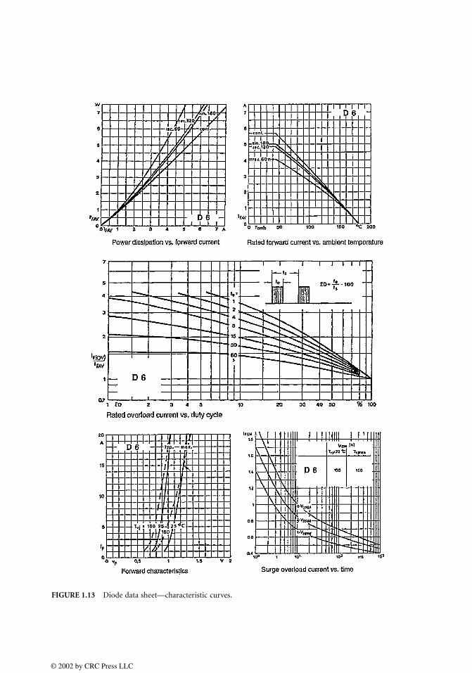
FIGURE 1.13 Diode data sheet—characteristic curves.
© 2002 by CRC Press LLC
Maximum Surge Current
The IFSM (forward surge maximum) rating is the maximum current that the diode can handle as anoccasional transient or from a circuit fault. The IFSM rating for the power diode D6 is up to 190 A, asshown in Fig 1.12.
Maximum Junction Temperature
This parameter defines the maximum junction temperature that a diode can withstand without failure.The maximum junction temperature for the power diode D6 is 180°C.
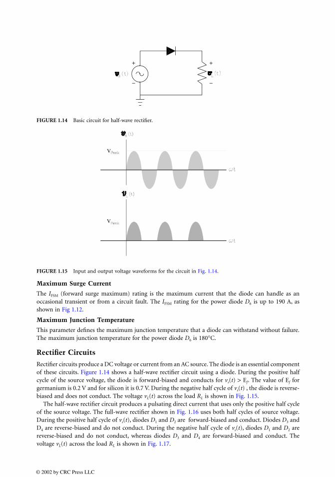
Rectifier Circuits
Rectifier circuits produce a DC voltage or current from an AC source. The diode is an essential componentof these circuits. Figure 1.14 shows a half-wave rectifier circuit using a diode. During the positive halfcycle of the source voltage, the diode is forward-biased and conducts for vs(t) > Ef. The value of Ef forgermanium is 0.2 V and for silicon it is 0.7 V. During the negative half cycle of vs(t) , the diode is reverse-biased and does not conduct. The voltage vL(t) across the load RL is shown in Fig. 1.15.
The half-wave rectifier circuit produces a pulsating direct current that uses only the positive half cycleof the source voltage. The full-wave rectifier shown in Fig. 1.16 uses both half cycles of source voltage.During the positive half cycle of vs(t), diodes D1 and D2 are forward-biased and conduct. Diodes D3 andD4 are reverse-biased and do not conduct. During the negative half cycle of vs(t), diodes D1 and D2 arereverse-biased and do not conduct, whereas diodes D3 and D4 are forward-biased and conduct. Thevoltage vL(t) across the load RL is shown in Fig. 1.17.
FIGURE 1.14 Basic circuit for half-wave rectifier.
FIGURE 1.15 Input and output voltage waveforms for the circuit in Fig. 1.14.
V
V
© 2002 by CRC Press LLC
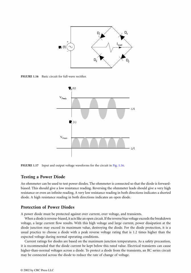
Testing a Power Diode
An ohmmeter can be used to test power diodes. The ohmmeter is connected so that the diode is forward-biased. This should give a low resistance reading. Reversing the ohmmeter leads should give a very highresistance or even an infinite reading. A very low resistance reading in both directions indicates a shorteddiode. A high resistance reading in both directions indicates an open diode.
Protection of Power Diodes
A power diode must be protected against over current, over voltage, and transients.When a diode is reverse-biased, it acts like an open circuit. If the reverse bias voltage exceeds the breakdown
voltage, a large current flow results. With this high voltage and large current, power dissipation at thediode junction may exceed its maximum value, destroying the diode. For the diode protection, it is ausual practice to choose a diode with a peak reverse voltage rating that is 1.2 times higher than theexpected voltage during normal operating conditions.
Current ratings for diodes are based on the maximum junction temperatures. As a safety precaution,it is recommended that the diode current be kept below this rated value. Electrical transients can causehigher-than-normal voltages across a diode. To protect a diode from the transients, an RC series circuitmay be connected across the diode to reduce the rate of change of voltage.
FIGURE 1.16 Basic circuit for full-wave rectifier.
FIGURE 1.17 Input and output voltage waveforms for the circuit in Fig. 1.16.
D1
D2D3
D4
(t)s
Iload
V
V
© 2002 by CRC Press LLC

1.3 Schottky Diodes
Sohail Anwar
Bonding a metal, such as aluminum or platinum, to n-type silicon forms a Schottky diode. The Schottkydiode is often used in integrated circuits for high-speed switching applications. An example of a high-speed switching application is a detector at microwave frequencies. The Schottky diode has a voltage-current characteristic similar to that of a silicon pn-junction diode. The Schottky is a subgroup of the TTLfamily and is designed to reduce the propagation delay time of the standard TTL IC chips. The constructionof the Schottky diode is shown in Fig. 1.18a, and its symbol is shown in Fig. 1.18b.
Characteristics
The low-noise characteristics of the Schottky diode make it ideal for application in power monitors oflow-level radio frequency, detectors for high frequency, and Doppler radar mixers. One of the mainadvantages of the Schottky barrier diode is its low forward voltage drop compared with that of a silicondiode. In the reverse direction, both the breakdown voltage and the capacitance of a Schottky barrier diodebehave very much like those of a one-sided step junction. In the one-sided step junction, the dopinglevel of the semiconductor determines the breakdown voltage. Because of the finite radius at the edgesof the diode and because of its sensitivity to surface cleanliness, the breakdown voltage is always somewhatlower than theoretical predictions.
Data Specifications
The data specification sheet for a DSS 20-0015B power Schottky diode is provided as an example inFigs. 1.19 and 1.20. Specifications will vary depending on the application and model of Schottky diode.
Testing of Schottky Diodes
Two ways of testing the diodes use either a voltmeter or a digital multimeter. The voltmeter should beset to the low resistance scale. A single diode or rectifier should read a low resistance, typically, 2/3 scalefrom the resistance in the forward direction. In the reverse direction, the resistance should be nearlyinfinite. It should not read near 0 Ω in the shorted or open directions. The diode will result in a higher
FIGURE 1.18 Diagram (a) and symbol (b) of the Schottky diode.
K
AA K
p-type substrate
SiO2
Metallic
n-type
n +
(a) (b)
© 2002 by CRC Press LLC

FIGURE 1.19 Data specification sheet for a DSS 20-00105B power Schottky diode (front). (Courtesy of IXYS.)
Power Schottky Rectifier
Features¥ International standard package
Very low VF
Extremely low switching lossesLow IRM-valuesEpoxy meets UL 94V-0
ApplicationsRectifiers in switch mode powersupplies (SMPS)Free wheeling diode in low voltageconverters
AdvantagesHigh reliability circuit operationLow voltage peaks for reducedprotection circuitsLow noise switchingLow losses
Dimensions see outlines.pdf
Pulse test: Pulse Width = 5 ms, Duty Cycle < 2.0 %Data according to IEC 60747 and per diode unless otherwise specified
IXYS reserves the right to change limits, Conditions and dimensions.
A C
C
A
TO-220 AC
C (TAB)
A = Anode, C = Cathode , TAB = Cathode
Symbol Conditions Maximum Ratings
IFRMS 35 AIFAVM TC = 135 C; rectangular, d = 0.5 20 A
IFSM TVJ = 45¡C; tp = 10 ms (50 Hz), sine 350 A
EAS IAS = tbd A; L = 180 H; T VJ = 25¡C; non repetitive tbd mJ
IAR VA =1.5 VRRM typ.; f=10 kHz; repetitive tbd A
(dv/dt)cr tbd V/ s
TVJ -55...+150 CTVJM 150 CTstg -55...+150 C
Ptot TC = 25 C 9 0 W
Md mounting torque 0.4...0.6 Nm
Weight typical 2 g
IFAV = 20 AVRRM = 15 VVF = 0.33 V
VRSM VRRM Type
V V
15 15 DSS 20-0015B
Symbol Conditions Characteristic Valuestyp. max.
IR TVJ = 25¡C VR = VRRM 10 mATVJ = 100¡C VR = VRRM 200 mA
VF IF = 20 A; TVJ = 125¡C 0.33 VIF = 20 A; TVJ = 25¡C 0.45 VIF = 40 A; TVJ = 125¡C 0.43 V
RthJC 1.4 K/WRthCH 0.5 K/W
Preliminary Data
© 2002 by CRC Press LLC
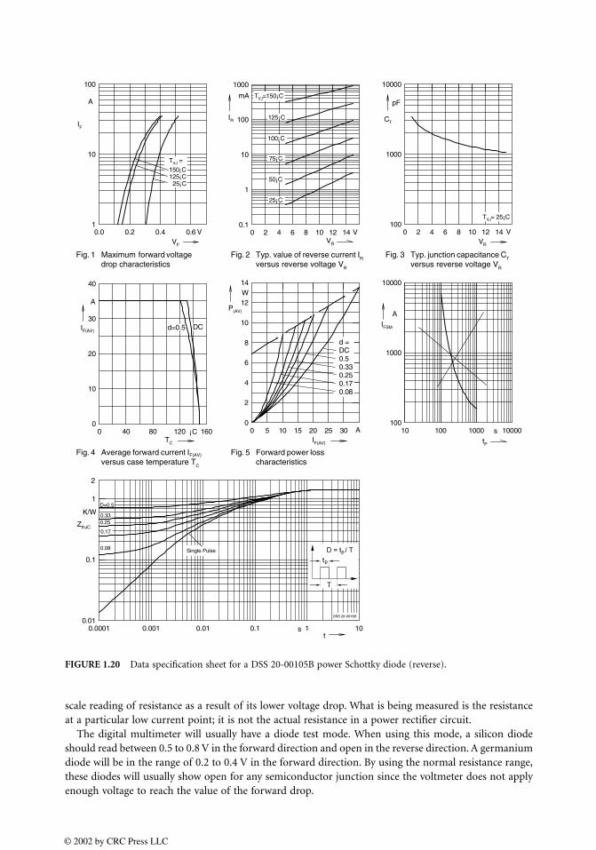
scale reading of resistance as a result of its lower voltage drop. What is being measured is the resistanceat a particular low current point; it is not the actual resistance in a power rectifier circuit.
The digital multimeter will usually have a diode test mode. When using this mode, a silicon diodeshould read between 0.5 to 0.8 V in the forward direction and open in the reverse direction. A germaniumdiode will be in the range of 0.2 to 0.4 V in the forward direction. By using the normal resistance range,these diodes will usually show open for any semiconductor junction since the voltmeter does not applyenough voltage to reach the value of the forward drop.
FIGURE 1.20 Data specification sheet for a DSS 20-00105B power Schottky diode (reverse).
0.0 0.2 0.4 0.61
10
100
0 2 4 6 8 10 12 140.1
1
10
100
1000
5 15 250 10 200
2
4
6
8
10
12
14
0.0001 0.001 0.01 0.1 1 100.01
0.1
1
0 40 80 120 1600
10
20
30
40
IF(AV)
TC
¡CIF(AV)
ts
K/W
00 10000
tP
0 2 4 6 8 10 12 14100
1000
10000
CTIR
IF
A
VFVR VR
V
pF
V
mA
A
P(AV)
W
ZthJC
V
Single Pulse
2
DSS 20-0015B
A
s
TVJ=150¡C
125¡C
100¡C
75¡C
25¡C
TVJ =
150¡C125¡C25¡C
TVJ= 25¡C
d=0.5
d =DC0.50.330.250.170.08
0.08
D=0.5
0.17
DC
50¡C
0.330.25
Fig. 3 Typ. junction capacitance CT
versus reverse voltage VR
Fig. 2 Typ. value of reverse current IR
versus reverse voltage VR
Fig. 1 Maximum forward voltagedrop characteristics
Fig. 4 Average forward current IF(AV)
versus case temperature TC
Fig. 5 Forward power losscharacteristics
30 10 100 10100
1000
10000
IFSM
A
© 2002 by CRC Press LLC

1.4 Thyristors
Sohail Anwar
Thyristors are four-layer pnpn power semiconductor devices. These devices switch between conductingand nonconducting states in response to a control signal. Thyristors are used in timing circuits, AC motorspeed control, light dimmers, and switching circuits. Small thyristors are also used as pulse sources forlarge thyristors. The thyristor family includes the silicon-controlled rectifier (SCR), the DIAC, the Triac,the silicon-controlled switch (SCS), and the gate turn-off thyristor (GTO).
The Basics of Silicon-Controlled Rectifiers (SCR)
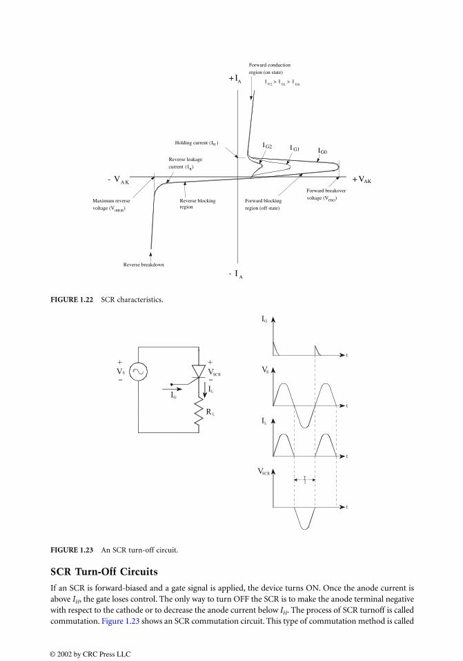
The SCR is the most commonly used electrical power controller. An SCR is sometimes called a pnpndiode because it conducts electrical current in only one direction. Figure 1.21a shows the SCR symbol.It has three terminals: the anode (A), the cathode (K), and the gate (G). The anode and the cathodeare the power terminals and the gate is the control terminal. The structure of an SCR is shown inFig. 1.21b.
When the SCR is forward-biased, that is, when the anode of an SCR is made more positive with respectto the cathode, the two outermost pn-junctions are forward-biased. The middle pn-junction is reverse-biased and the current cannot flow. If a small gate current is now applied, it forward-biases the middle pn-junction and allows a much larger current to flow through the device. The SCR stays ON even if the gatecurrent is removed. SCR shutoff occurs only when the anode current becomes less than a level called theholding current (IH).
Characteristics
The volt-ampere characteristic of an SCR is shown in Fig. 1.22. If the forward bias is increased to theforward breakover voltage, VFBO, the SCR turns ON. The value of forward breakover voltage is controlledby the gate current IG. If the gate-cathode pn-junction is forward-biased, the SCR is turned ON at a lowerbreakover voltage than with the gate open. As shown in Fig. 1.22, the breakover voltage decreases withan increase in the gate current. At a low gate current, the SCR turns ON at a lower forward anode voltage.At a higher gate current, the SCR turns ON at a still lower value of forward anode voltage.
When the SCR is reverse-biased, there is a small reverse leakage current (IR). If the reverse bias isincreased until the voltage reaches the reverse breakdown voltage (V(BR)R), the reverse current will increasesharply. If the current is not limited to a safe value, the SCR may be destroyed.
FIGURE 1.21 (a) The SCR symbol; (b) the SCR structure.
G
K
A
(anode)
(cathode)
(gate)
(a) (b)
© 2002 by CRC Press LLC
SCR Turn-Off Circuits
If an SCR is forward-biased and a gate signal is applied, the device turns ON. Once the anode current isabove IH, the gate loses control. The only way to turn OFF the SCR is to make the anode terminal negativewith respect to the cathode or to decrease the anode current below IH. The process of SCR turnoff is calledcommutation. Figure 1.23 shows an SCR commutation circuit. This type of commutation method is called
FIGURE 1.22 SCR characteristics.
FIGURE 1.23 An SCR turn-off circuit.
Holding current (I )
+ I
+ V
Forward conduction
region (on state)
Forward blocking
region (off state)
Forward breakover
voltage (VFBO) Reverse blockingregion
Reverse leakage
current (IR)
Maximum reverse
voltage (V(BR)R)
Reverse breakdown
I > I > I
G2I I G1 G0I
G2 G1 G0A
A- I
A K- V
H
AK
© 2002 by CRC Press LLC
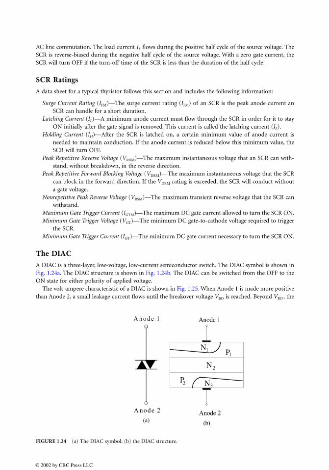
AC line commutation. The load current IL flows during the positive half cycle of the source voltage. TheSCR is reverse-biased during the negative half cycle of the source voltage. With a zero gate current, theSCR will turn OFF if the turn-off time of the SCR is less than the duration of the half cycle.
SCR Ratings
A data sheet for a typical thyristor follows this section and includes the following information:
Surge Current Rating (IFM)—The surge current rating (IFM) of an SCR is the peak anode current anSCR can handle for a short duration.
Latching Current (IL)—A minimum anode current must flow through the SCR in order for it to stayON initially after the gate signal is removed. This current is called the latching current (IL).
Holding Current (IH)—After the SCR is latched on, a certain minimum value of anode current isneeded to maintain conduction. If the anode current is reduced below this minimum value, theSCR will turn OFF.
Peak Repetitive Reverse Voltage (VRRM)—The maximum instantaneous voltage that an SCR can with-stand, without breakdown, in the reverse direction.
Peak Repetitive Forward Blocking Voltage (VDRM)—The maximum instantaneous voltage that the SCRcan block in the forward direction. If the VDRM rating is exceeded, the SCR will conduct withouta gate voltage.
Nonrepetitive Peak Reverse Voltage (VRSM)—The maximum transient reverse voltage that the SCR canwithstand.
Maximum Gate Trigger Current (IGTM)—The maximum DC gate current allowed to turn the SCR ON.Minimum Gate Trigger Voltage (VGT)—The minimum DC gate-to-cathode voltage required to trigger
the SCR.Minimum Gate Trigger Current (IGT)—The minimum DC gate current necessary to turn the SCR ON.
The DIAC
A DIAC is a three-layer, low-voltage, low-current semiconductor switch. The DIAC symbol is shown inFig. 1.24a. The DIAC structure is shown in Fig. 1.24b. The DIAC can be switched from the OFF to theON state for either polarity of applied voltage.
The volt-ampere characteristic of a DIAC is shown in Fig. 1.25. When Anode 1 is made more positivethan Anode 2, a small leakage current flows until the breakover voltage VBO is reached. Beyond VBO, the
FIGURE 1.24 (a) The DIAC symbol; (b) the DIAC structure.
A node 1
A node 2
(a)
N
P
P
N
N
Anode 2
Anode 1
1
2
2
1
3
(b)
© 2002 by CRC Press LLC
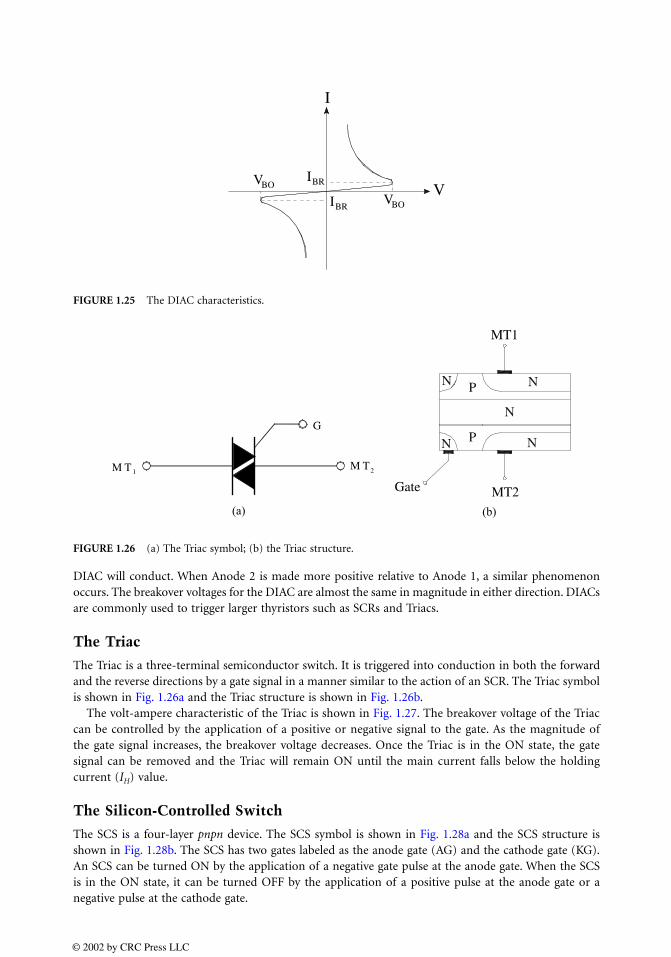
DIAC will conduct. When Anode 2 is made more positive relative to Anode 1, a similar phenomenonoccurs. The breakover voltages for the DIAC are almost the same in magnitude in either direction. DIACsare commonly used to trigger larger thyristors such as SCRs and Triacs.
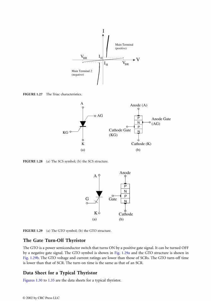
The Triac
The Triac is a three-terminal semiconductor switch. It is triggered into conduction in both the forwardand the reverse directions by a gate signal in a manner similar to the action of an SCR. The Triac symbolis shown in Fig. 1.26a and the Triac structure is shown in Fig. 1.26b.
The volt-ampere characteristic of the Triac is shown in Fig. 1.27. The breakover voltage of the Triaccan be controlled by the application of a positive or negative signal to the gate. As the magnitude ofthe gate signal increases, the breakover voltage decreases. Once the Triac is in the ON state, the gatesignal can be removed and the Triac will remain ON until the main current falls below the holdingcurrent (IH) value.
The Silicon-Controlled Switch
The SCS is a four-layer pnpn device. The SCS symbol is shown in Fig. 1.28a and the SCS structure isshown in Fig. 1.28b. The SCS has two gates labeled as the anode gate (AG) and the cathode gate (KG).An SCS can be turned ON by the application of a negative gate pulse at the anode gate. When the SCSis in the ON state, it can be turned OFF by the application of a positive pulse at the anode gate or anegative pulse at the cathode gate.
FIGURE 1.25 The DIAC characteristics.
FIGURE 1.26 (a) The Triac symbol; (b) the Triac structure.
I
VBOV
BOVBRI
BRI
M T 2
G
M T1
(a)
N
P
P
N
N
N
N
Gate MT2
MT1
(b)
© 2002 by CRC Press LLC
The Gate Turn-Off Thyristor
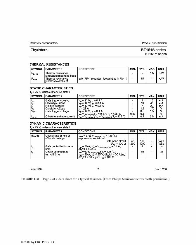
The GTO is a power semiconductor switch that turns ON by a positive gate signal. It can be turned OFFby a negative gate signal. The GTO symbol is shown in Fig. 1.29a and the GTO structure is shown inFig. 1.29b. The GTO voltage and current ratings are lower than those of SCRs. The GTO turn-off timeis lower than that of SCR. The turn-on time is the same as that of an SCR.
Data Sheet for a Typical Thyristor
Figures 1.30 to 1.35 are the data sheets for a typical thyristor.
FIGURE 1.27 The Triac characteristics.
FIGURE 1.28 (a) The SCS symbol; (b) the SCS structure.
FIGURE 1.29 (a) The GTO symbol; (b) the GTO structure.
I
V
BRV HI
BRVHI
Main Terminal 2(negative)
Main Terminal(positive)
A
K
AG
KG
(a)
Anode (A)
Cathode (K)
Anode Gate(AG)
Cathode Gate(KG)
(b)
A
K
G
(a)
Anode
Cathode
Gate
(b)
© 2002 by CRC Press LLC
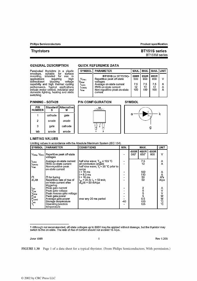
FIGURE 1.30 Page 1 of a data sheet for a typical thyristor. (From Philips Semiconductors. With permission.)
© 2002 by CRC Press LLC
© 2002 by CRC Press LLC
FIGURE 1.31 Page 2 of a data sheet for a typical thyristor. (From Philips Semiconductors. With permission.)
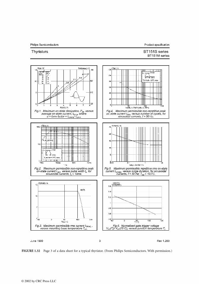
FIGURE 1.32 Page 3 of a data sheet for a typical thyristor. (From Philips Semiconductors. With permission.)
© 2002 by CRC Press LLC
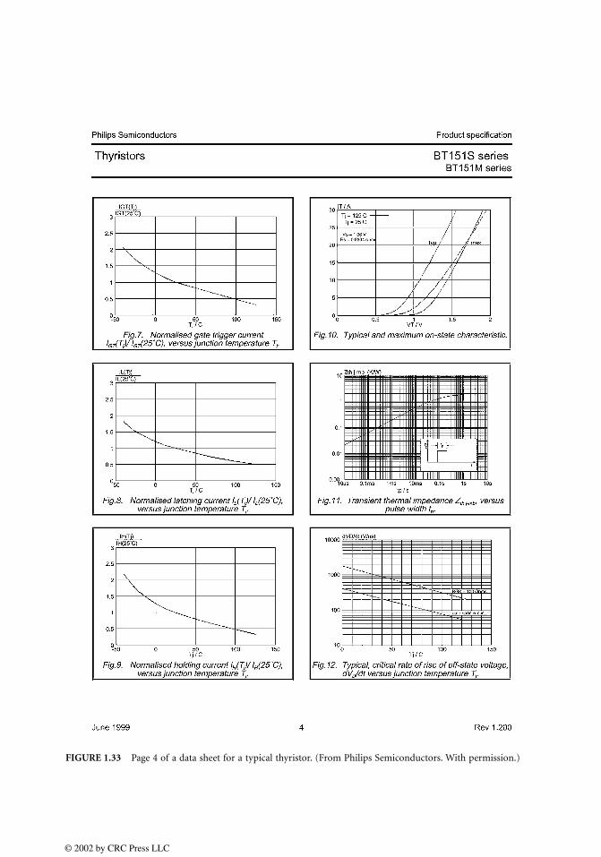
FIGURE 1.33 Page 4 of a data sheet for a typical thyristor. (From Philips Semiconductors. With permission.)
© 2002 by CRC Press LLC

© 2002 by CRC Press LLC
FIGURE 1.34 Page 5 of a data sheet for a typical thyristor. (From Philips Semiconductors. With permission.)

1.5 Power Bipolar Junction Transistors
Sohail Anwar
Power bipolar junction transistors (BJTs) play a vital role in power circuits. Like most other power devices,power transistors are generally constructed using silicon. The use of silicon allows operation of a BJT athigher currents and junction temperatures, which leads to the use of power transistors in AC applicationswhere ranges of up to several hundred kilowatts are essential.
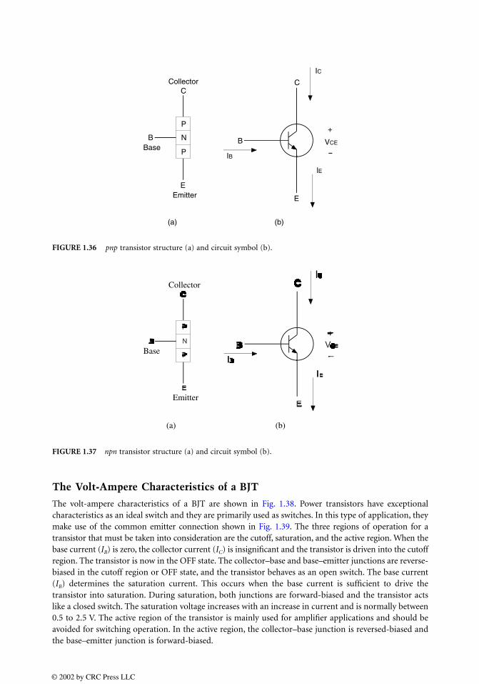
The power transistor is part of a family of three-layer devices. The three layers or terminals of a transistorare the base, the collector, and the emitter. Effectively, the transistor is equivalent to having two pn-diodejunctions stacked in opposite directions to each other. The two types of a transistor are termed npn andpnp. The npn-type transistor has a higher current-to-voltage rating than the pnp and is preferred for mostpower conversion applications. The easiest way to distinguish an npn-type transistor from a pnp-type isby virtue of the schematic or circuit symbol. The pnp type has an arrowhead on the emitter that pointstoward the base. Figure 1.36 shows the structure and the symbol of a pnp-type transistor. The npn-typetransistor has an arrowhead pointing away from the base. Figure 1.37 shows the structure and the symbolof an npn-type transistor.
When used as a switch, the transistor controls the power from the source to the load by supplying sufficientbase current. This small current from the driving circuit through the base–emitter, which must be maintained,turns on the collector—emitter path. Removing the current from the base–emitter path and making the basevoltage slightly negative turns off the switch. Even though the base–emitter path may only utilize a smallamount of current, the collector–emitter path is capable of carrying a much higher current.
FIGURE 1.35 Page 6 of a data sheet for a typical thyristor. (From Philips Semiconductors. With permission.)
© 2002 by CRC Press LLC
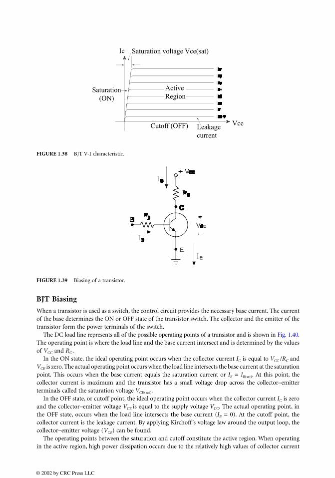
The Volt-Ampere Characteristics of a BJT
The volt-ampere characteristics of a BJT are shown in Fig. 1.38. Power transistors have exceptionalcharacteristics as an ideal switch and they are primarily used as switches. In this type of application, theymake use of the common emitter connection shown in Fig. 1.39. The three regions of operation for atransistor that must be taken into consideration are the cutoff, saturation, and the active region. When thebase current (IB) is zero, the collector current (IC) is insignificant and the transistor is driven into the cutoffregion. The transistor is now in the OFF state. The collector–base and base–emitter junctions are reverse-biased in the cutoff region or OFF state, and the transistor behaves as an open switch. The base current(IB) determines the saturation current. This occurs when the base current is sufficient to drive thetransistor into saturation. During saturation, both junctions are forward-biased and the transistor actslike a closed switch. The saturation voltage increases with an increase in current and is normally between0.5 to 2.5 V. The active region of the transistor is mainly used for amplifier applications and should beavoided for switching operation. In the active region, the collector–base junction is reversed-biased andthe base–emitter junction is forward-biased.
FIGURE 1.36 pnp transistor structure (a) and circuit symbol (b).
FIGURE 1.37 npn transistor structure (a) and circuit symbol (b).
Collector
Base
Emitter
(a) (b)
P
N
P
E
B
C
B
C
E
IC
+
VCE
--
lE
IB
Collector
Base
Emitter
(a) (b)
© 2002 by CRC Press LLC
BJT Biasing
When a transistor is used as a switch, the control circuit provides the necessary base current. The currentof the base determines the ON or OFF state of the transistor switch. The collector and the emitter of thetransistor form the power terminals of the switch.
The DC load line represents all of the possible operating points of a transistor and is shown in Fig. 1.40.The operating point is where the load line and the base current intersect and is determined by the valuesof VCC and RC .
In the ON state, the ideal operating point occurs when the collector current IC is equal to VCC /RC andVCE is zero. The actual operating point occurs when the load line intersects the base current at the saturationpoint. This occurs when the base current equals the saturation current or IB = IB(sat). At this point, thecollector current is maximum and the transistor has a small voltage drop across the collector–emitterterminals called the saturation voltage VCE(sat).
In the OFF state, or cutoff point, the ideal operating point occurs when the collector current IC is zeroand the collector–emitter voltage VCE is equal to the supply voltage VCC. The actual operating point, inthe OFF state, occurs when the load line intersects the base current (IB = 0). At the cutoff point, thecollector current is the leakage current. By applying Kirchoff ’s voltage law around the output loop, thecollector–emitter voltage (VCE) can be found.
The operating points between the saturation and cutoff constitute the active region. When operatingin the active region, high power dissipation occurs due to the relatively high values of collector current
FIGURE 1.38 BJT V-I characteristic.
FIGURE 1.39 Biasing of a transistor.
Saturation voltage Vce(sat)
ActiveRegion
Saturation (ON)
Cutoff (OFF) Leakagecurrent
Ic
Vce
© 2002 by CRC Press LLC
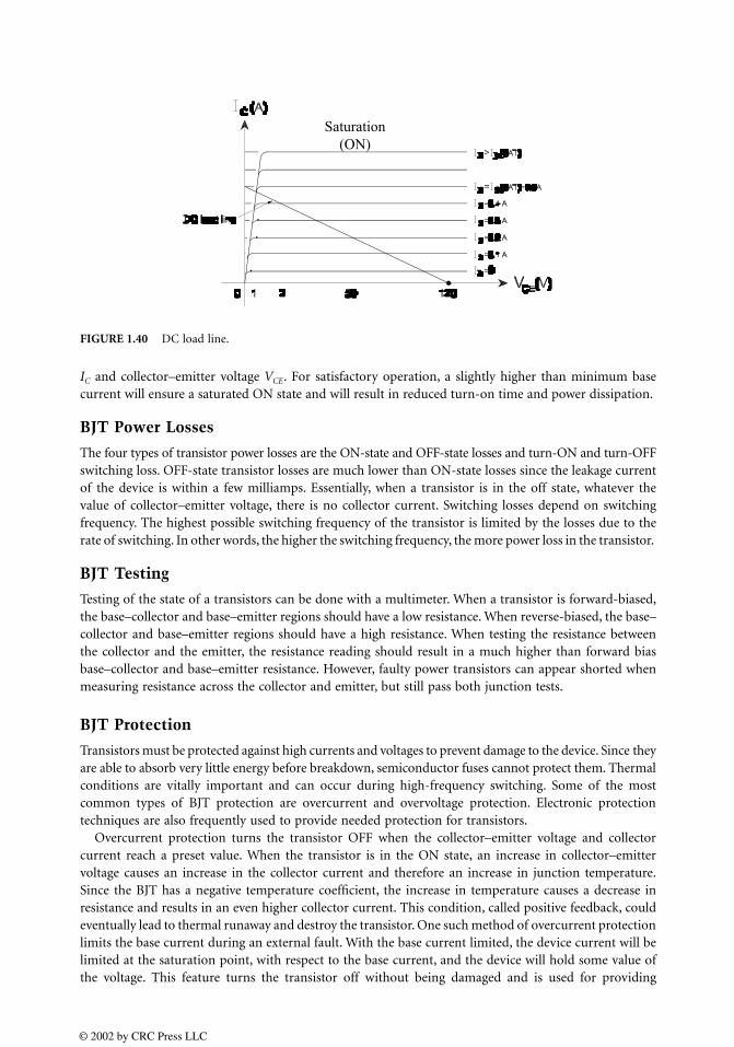
IC and collector–emitter voltage VCE. For satisfactory operation, a slightly higher than minimum basecurrent will ensure a saturated ON state and will result in reduced turn-on time and power dissipation.
BJT Power Losses
The four types of transistor power losses are the ON-state and OFF-state losses and turn-ON and turn-OFFswitching loss. OFF-state transistor losses are much lower than ON-state losses since the leakage currentof the device is within a few milliamps. Essentially, when a transistor is in the off state, whatever thevalue of collector–emitter voltage, there is no collector current. Switching losses depend on switchingfrequency. The highest possible switching frequency of the transistor is limited by the losses due to therate of switching. In other words, the higher the switching frequency, the more power loss in the transistor.
BJT Testing
Testing of the state of a transistors can be done with a multimeter. When a transistor is forward-biased,the base–collector and base–emitter regions should have a low resistance. When reverse-biased, the base–collector and base–emitter regions should have a high resistance. When testing the resistance betweenthe collector and the emitter, the resistance reading should result in a much higher than forward biasbase–collector and base–emitter resistance. However, faulty power transistors can appear shorted whenmeasuring resistance across the collector and emitter, but still pass both junction tests.
BJT Protection
Transistors must be protected against high currents and voltages to prevent damage to the device. Since theyare able to absorb very little energy before breakdown, semiconductor fuses cannot protect them. Thermalconditions are vitally important and can occur during high-frequency switching. Some of the mostcommon types of BJT protection are overcurrent and overvoltage protection. Electronic protectiontechniques are also frequently used to provide needed protection for transistors.
Overcurrent protection turns the transistor OFF when the collector–emitter voltage and collectorcurrent reach a preset value. When the transistor is in the ON state, an increase in collector–emittervoltage causes an increase in the collector current and therefore an increase in junction temperature.Since the BJT has a negative temperature coefficient, the increase in temperature causes a decrease inresistance and results in an even higher collector current. This condition, called positive feedback, couldeventually lead to thermal runaway and destroy the transistor. One such method of overcurrent protectionlimits the base current during an external fault. With the base current limited, the device current will belimited at the saturation point, with respect to the base current, and the device will hold some value ofthe voltage. This feature turns the transistor off without being damaged and is used for providing
FIGURE 1.40 DC load line.
Saturation (ON)
© 2002 by CRC Press LLC
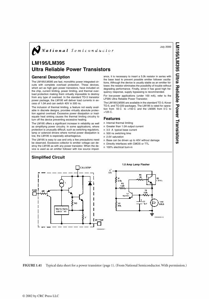
FIGURE 1.41 Typical data sheet for a power transistor (page 1). (From National Semiconductor. With permission.)
LM195/LM395Ultra Reliable Power TransistorsGeneral DescriptionThe LM195/LM395 are fast, monolithic power integrated cir-cuits with complete overload protection. These devices,which act as high gain power transistors, have included onthe chip, current limiting, power limiting, and thermal over-load protection making them virtually impossible to destroyfrom any type of overload. In the standard TO-3 transistorpower package, the LM195 will deliver load currents in ex-cess of 1.0A and can switch 40V in 500 ns.
The inclusion of thermal limiting, a feature not easily avail-able in discrete designs, provides virtually absolute protec-tion against overload. Excessive power dissipation or inad-equate heat sinking causes the thermal limiting circuitry toturn off the device preventing excessive heating.
The LM195 offers a significant increase in reliability as wellas simplifying power circuitry. In some applications, whereprotection is unusually difficult, such as switching regulators,lamp or solenoid drivers where normal power dissipation islow, the LM195 is especially advantageous.
The LM195 is easy to use and only a few precautions needbe observed. Excessive collector to emitter voltage can de-stroy the LM195 as with any power transistor. When the de-vice is used as an emitter follower with low source imped-
ance, it is necessary to insert a 5.0k resistor in series withthe base lead to prevent possible emitter follower oscilla-tions. Although the device is usually stable as an emitter fol-lower, the resistor eliminates the possibility of trouble withoutdegrading performance. Finally, since it has good high fre-quency response, supply bypassing is recommended.
For low-power applications (under 100 mA), refer to theLP395 Ultra Reliable Power Transistor.
The LM195/LM395 are available in the standard TO-3, KovarTO-5, and TO-220 packages. The LM195 is rated for opera-tion from 55 C to +150 C and the LM395 from 0 C to+125 C.
Featuresn Internal thermal limitingn Greater than 1.0A output currentn 3.0 A typical base currentn 500 ns switching timen 2.0V saturationn Base can be driven up to 40V without damagen Directly interfaces with CMOS or TTLn 100% electrical burn-in
Simplified Circuit
DS006009-1
1.0 Amp Lamp Flasher
DS006009-16
July 2000
LM195/LM
395U
ltraR
eliableP
ower
Transistors
© 2002 by CRC Press LLC
© 2002 by CRC Press LLC
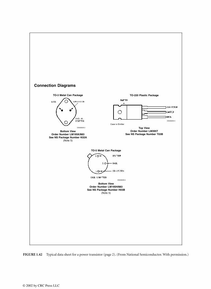
FIGURE 1.42 Typical data sheet for a power transistor (page 2). (From National Semiconductor. With permission.)
Connection Diagrams
TO-3 Metal Can Package
DS006009-2
Bottom ViewOrder Number LM195K/883
See NS Package Number K02A(Note 5)
TO-220 Plastic Package
DS006009-3
Case is Emitter
Top ViewOrder Number LM395T
See NS Package Number T03B
TO-5 Metal Can Package
DS006009-4
Bottom ViewOrder Number LM195H/883
See NS Package Number H03B(Note 5)

© 2002 by CRC Press LLC
FIGURE 1.43 Typical data sheet for a power transistor (page 3). (From National Semiconductor. With permission.)
Absolute Maximum Ratings (Note 1)
If Military/Aerospace specified devices are required,please contact the National Semiconductor Sales Office/Distributors for availability and specifications.
Collector to Emitter VoltageLM195 42VLM395 36V
Collector to Base VoltageLM195 42VLM395 36V
Base to Emitter Voltage (Forward)LM195LM395
42V36V
Base to Emitter Voltage (Reverse) 20VCollector Current Internally LimitedPower Dissipation Internally LimitedOperating Temperature Range
LM195 55 C to +150 CLM395 0 C to +125 C
Storage Temperature Range 65 C to +150 CLead Temperature
(Soldering, 10 sec.) 260 C
Preconditioning100% Burn-In In Thermal Limit
Electrical Characteristics(Note 2)
Parameter Conditions LM195 LM395 Units
Min Typ Max Min Typ Max
Collector-Emitter Operating Voltage IQ ≤ IC ≤ IMAX 42 36 V
(Note 4)
Base to Emitter Breakdown Voltage 0 ≤ VCE ≤ VCEMAX 42 36 60 V
Collector Current
TO-3, TO-220 VCE ≤ 15V 1.2 2.2 1.0 2.2 A
TO-5 VCE ≤ 7.0V 1.2 1.8 1.0 1.8 A
Saturation Voltage IC ≤ 1.0A, TA = 25 C 1.8 2.0 1.8 2.2 V
Base Current 0 ≤ IC ≤ IMAX 3.0 5.0 3.0 10 A0 ≤ VCE ≤ VCEMAX
Quiescent Current (IQ) Vbe = 02.0 5.0 2.0 10 mA
0 ≤ VCE ≤ VCEMAX
Base to Emitter Voltage IC = 1.0A, TA = +25 C 0.9 0.9 V
Switching Time VCE = 36V, RL = 36Ω,500 500 ns
TA = 25 C
Thermal Resistance Junction to TO-3 Package (K) 2.3 3.0 2.3 3.0 C/W
Case (Note 3) TO-5 Package (H) 12 15 12 15 C/W
TO-220 Package (T) 4 6 C/W
Note 1: »AbsoluteMaximum Ratings…indicate limits beyond which damage to the device may occur. Operating Ratings indicate conditions for which the device isfunctional, but do not guarantee specific performance limits.
Note 2: Unless otherwise specified, these specifications apply for 55 C ≤ Tj ≤ +150 C for the LM195 and 0 C ≤ +125 C for the LM395.
Note 3: Without a heat sink, the thermal resistance of the TO-5 package is about +150 C/W, while that of the TO-3 package is +35 C/W.
Note 4: Selected devices with higher breakdown available.
Note 5: Refer to RETS195H and RETS195K drawings of military LM195H and LM195K versions for specifications.
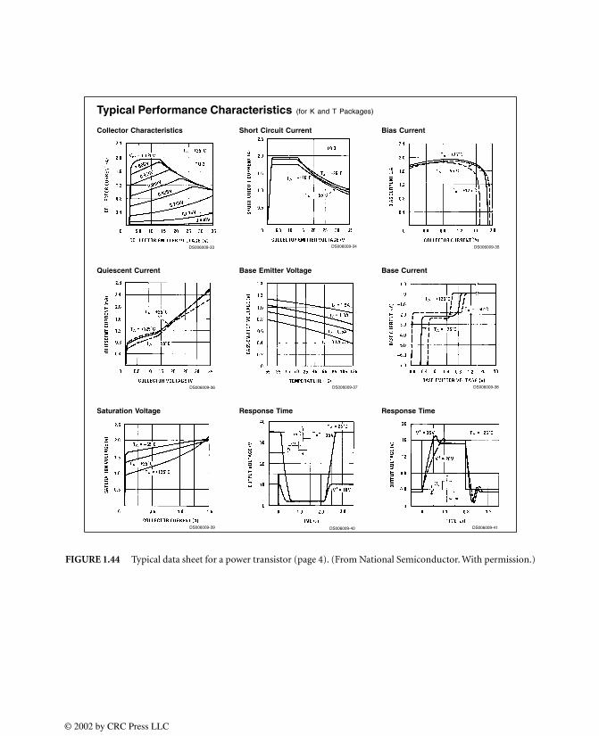
© 2002 by CRC Press LLC
FIGURE 1.44 Typical data sheet for a power transistor (page 4). (From National Semiconductor. With permission.)
Typical Performance Characteristics (for K and T Packages)
Collector Characteristics
DS006009-33
Short Circuit Current
DS006009-34
Bias Current
DS006009-35
Quiescent Current
DS006009-36
Base Emitter Voltage
DS006009-37
Base Current
DS006009-38
Saturation Voltage
DS006009-39
Response Time
DS006009-40
Response Time
DS006009-41

© 2002 by CRC Press LLC
FIGURE 1.45 Typical data sheet for a power transistor (page 5). (From National Semiconductor. With permission.)
Typical Performance Characteristics (for K and T Packages) (Continued)
10V Transfer Function
DS006009-7
36V Transfer Function
DS006009-8
Transconductance
DS006009-9
Small Signal FrequencyResponse
DS006009-10
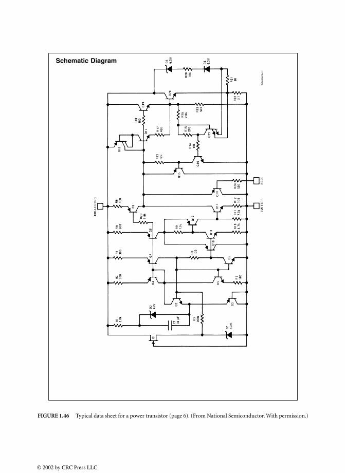
© 2002 by CRC Press LLC
FIGURE 1.46 Typical data sheet for a power transistor (page 6). (From National Semiconductor. With permission.)
Schematic Diagram
DS
0060
09-1
1
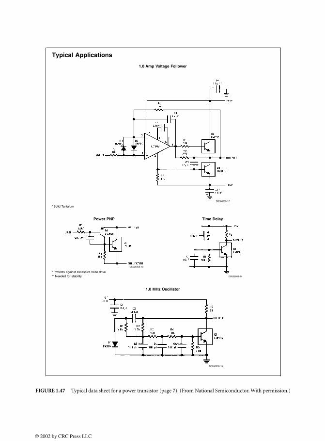
© 2002 by CRC Press LLC
FIGURE 1.47 Typical data sheet for a power transistor (page 7). (From National Semiconductor. With permission.)
Typical Applications
1.0 Amp Voltage Follower
DS006009-12
*Solid Tantalum
Power PNP
DS006009-13
*Protects against excessive base drive** Needed for stability
Time Delay
DS006009-14
1.0 MHz Oscillator
DS006009-15
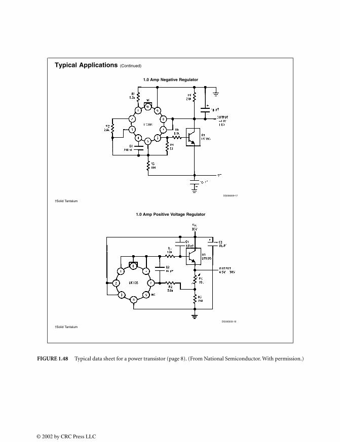
© 2002 by CRC Press LLC
FIGURE 1.48 Typical data sheet for a power transistor (page 8). (From National Semiconductor. With permission.)
Typical Applications (Continued)
1.0 Amp Negative Regulator
DS006009-17
†Solid Tantalum
1.0 Amp Positive Voltage Regulator
DS006009-18
†Solid Tantalum
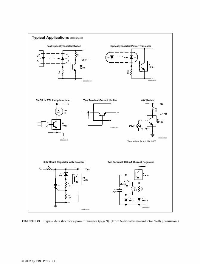
© 2002 by CRC Press LLC
FIGURE 1.49 Typical data sheet for a power transistor (page 9). (From National Semiconductor. With permission.)
Typical Applications (Continued)
Fast Optically Isolated Switch
DS006009-19
Optically Isolated Power Transistor
DS006009-20
CMOS or TTL Lamp Interface
DS006009-21
Two Terminal Current Limiter
DS006009-22
40V Switch
DS006009-23
*Drive Voltage 0V to ≥ 10V ≤ 42V
6.0V Shunt Regulator with Crowbar
DS006009-24
Two Terminal 100 mA Current Regulator
DS006009-25
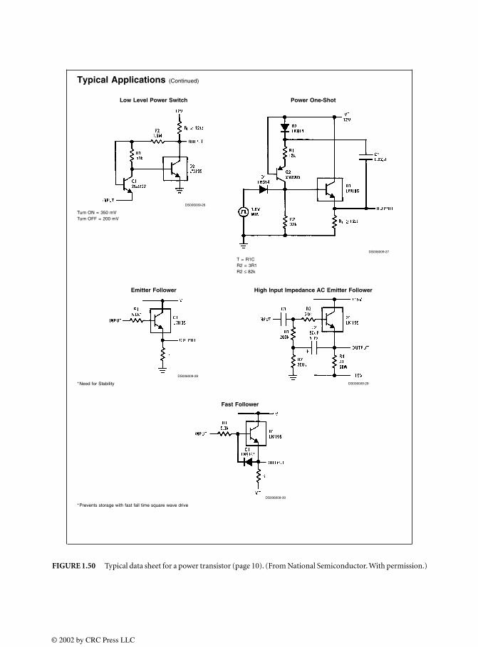
© 2002 by CRC Press LLC
FIGURE 1.50 Typical data sheet for a power transistor (page 10). (From National Semiconductor. With permission.)
Typical Applications (Continued)
Low Level Power Switch
DS006009-26
Turn ON = 350 mVTurn OFF = 200 mV
Power One-Shot
DS006009-27
T = R1CR2 = 3R1R2 ≤ 82k
Emitter Follower
DS006009-28
*Need for Stability
High Input Impedance AC Emitter Follower
DS006009-29
Fast Follower
DS006009-30
*Prevents storage with fast fall time square wave drive
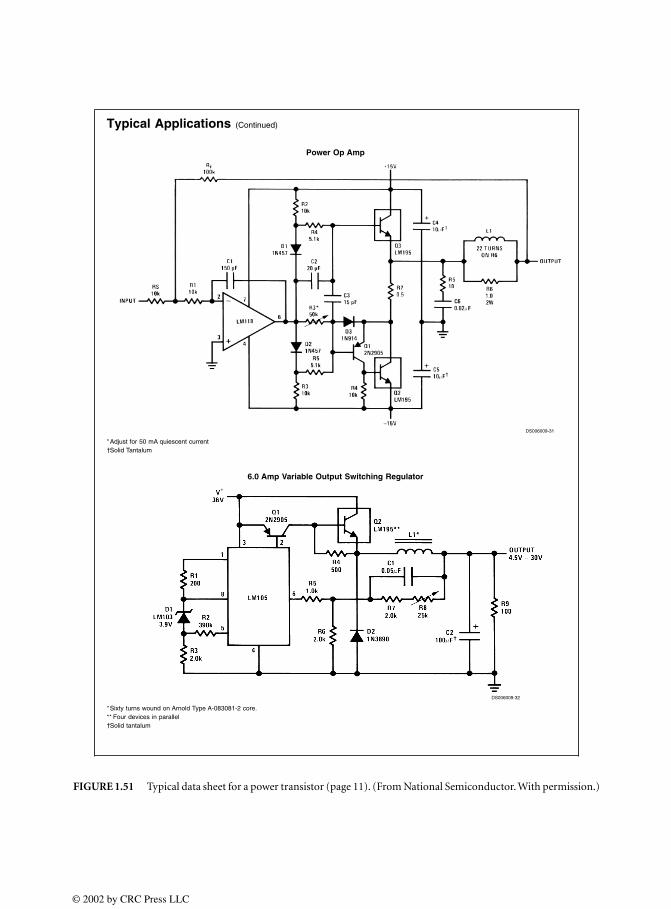
© 2002 by CRC Press LLC
FIGURE 1.51 Typical data sheet for a power transistor (page 11). (From National Semiconductor. With permission.)
Typical Applications (Continued)
Power Op Amp
DS006009-31
*Adjust for 50 mA quiescent current†Solid Tantalum
6.0 Amp Variable Output Switching Regulator
DS006009-32
*Sixty turns wound on Arnold Type A-083081-2 core.** Four devices in parallel†Solid tantalum
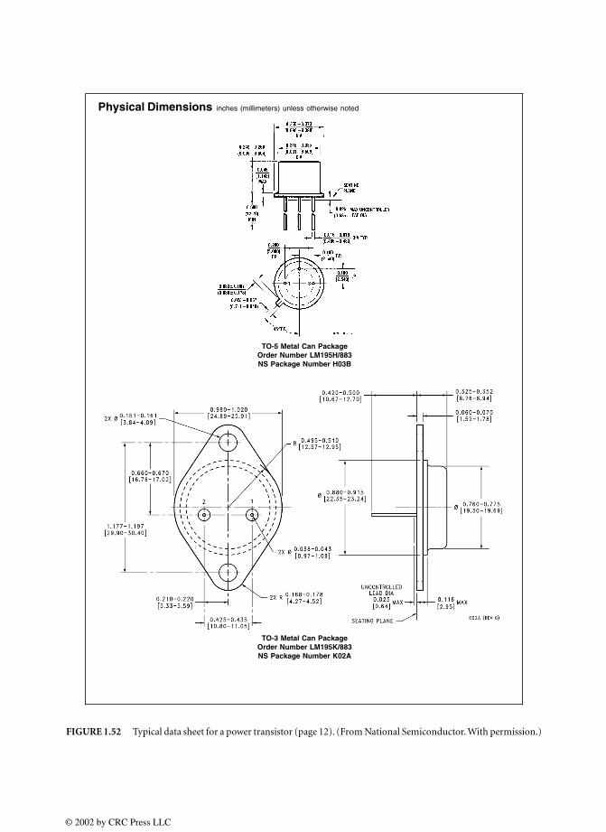
© 2002 by CRC Press LLC
FIGURE 1.52 Typical data sheet for a power transistor (page 12). (From National Semiconductor. With permission.)
Physical Dimensions inches (millimeters) unless otherwise noted
TO-5 Metal Can PackageOrder Number LM195H/883NS Package Number H03B
TO-3 Metal Can PackageOrder Number LM195K/883NS Package Number K02A
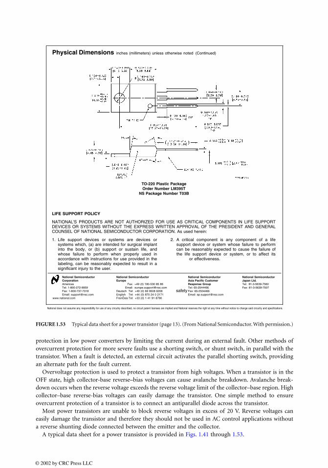
protection in low power converters by limiting the current during an external fault. Other methods ofovercurrent protection for more severe faults use a shorting switch, or shunt switch, in parallel with thetransistor. When a fault is detected, an external circuit activates the parallel shorting switch, providingan alternate path for the fault current.
Overvoltage protection is used to protect a transistor from high voltages. When a transistor is in theOFF state, high collector-base reverse–bias voltages can cause avalanche breakdown. Avalanche break-down occurs when the reverse voltage exceeds the reverse voltage limit of the collector–base region. Highcollector–base reverse-bias voltages can easily damage the transistor. One simple method to ensureovercurrent protection of a transistor is to connect an antiparallel diode across the transistor.
Most power transistors are unable to block reverse voltages in excess of 20 V. Reverse voltages caneasily damage the transistor and therefore they should not be used in AC control applications withouta reverse shunting diode connected between the emitter and the collector.
A typical data sheet for a power transistor is provided in Figs. 1.41 through 1.53.
FIGURE 1.53 Typical data sheet for a power transistor (page 13). (From National Semiconductor. With permission.)
Physical Dimensions inches (millimeters) unless otherwise noted (Continued)
LIFE SUPPORT POLICY
NATIONAL'S PRODUCTS ARE NOT AUTHORIZED FOR USE AS CRITICAL COMPONENTS IN LIFE SUPPORTDEVICES OR SYSTEMS WITHOUT THE EXPRESS WRITTEN APPROVAL OF THE PRESIDENT AND GENERALCOUNSEL OF NATIONAL SEMICONDUCTOR CORPORATION. As used herein:
1. Life support devices or systems are devices orsystems which, (a) are intended for surgical implantinto the body, or (b) support or sustain life, andwhose failure to perform when properly used inaccordance with instructions for use provided in thelabeling, can be reasonably expected to result in asignificant injury to the user.
2. A critical component is any component of a lifesupport device or system whose failure to performcan be reasonably expected to cause the failure ofthe life support device or system, or to affect its
safety
or effectiveness.
National SemiconductorCorporationAmericasTel: 1-800-272-9959Fax: 1-800-737-7018Email: [email protected]
National SemiconductorEurope
Fax: +49 (0) 180-530 85 86Email: [email protected]
Deutsch Tel: +49 (0) 69 9508 6208English Tel: +44 (0) 870 24 0 2171FranÕais Tel: +33 (0) 1 41 91 8790
National SemiconductorAsia Pacific CustomerResponse GroupTel: 65-2544466Fax: 65-2504466Email: [email protected]
National SemiconductorJapan Ltd.Tel: 81-3-5639-7560Fax: 81-3-5639-7507
www.national.com
TO-220 Plastic PackageOrder Number LM395T
NS Package Number T03B
National does not assume any responsibility for use of any circuitry described, no circuit patent licenses are implied and National reserves the right at any time without notice to change said circuitry and specifications.
© 2002 by CRC Press LLC
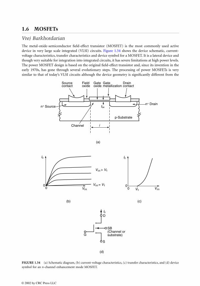
1.6 MOSFETs
Vrej Barkhordarian
The metal-oxide-semiconductor field-effect transistor (MOSFET) is the most commonly used activedevice in very large scale integrated (VLSI) circuits. Figure 1.54 shows the device schematic, current-voltage characteristics, transfer characteristics and device symbol for a MOSFET. It is a lateral device andthough very suitable for integration into integrated circuits, it has severe limitations at high power levels.The power MOSFET design is based on the original field-effect transistor and, since its invention in theearly 1970s, has gone through several evolutionary steps. The processing of power MOSFETs is verysimilar to that of today’s VLSI circuits although the device geometry is significantly different from the
FIGURE 1.54 (a) Schematic diagram, (b) current-voltage characteristics, (c) transfer characteristics, and (d) devicesymbol for an n-channel enhancement mode MOSFET.
Sourcecontact
Fieldoxide
Gateoxide
Draincontact
p-Substrate
Gatemetallization
n+ Drainn+ Source
Channel
(a)
(b)
(d)
(c)
00
00
D
G
S
SB(Channel orsubstrate)
tox
lD lD
lD
VDS
VGS = Vτ
VGS > Vτ
i
Vτ VGS
© 2002 by CRC Press LLC
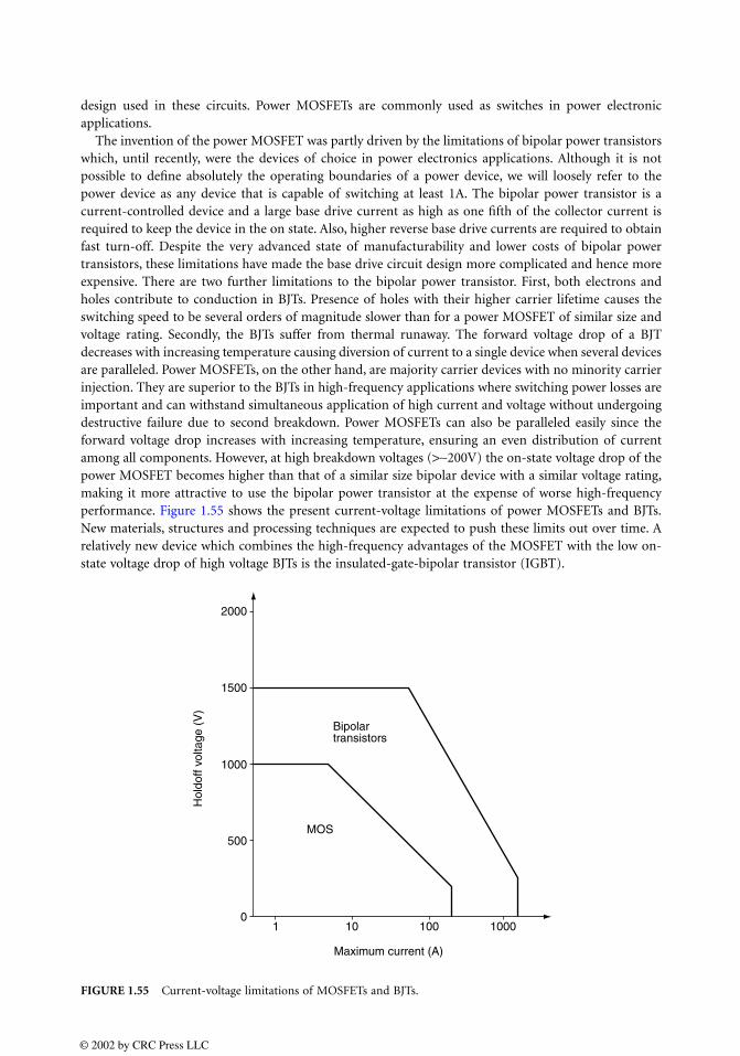
design used in these circuits. Power MOSFETs are commonly used as switches in power electronicapplications.
The invention of the power MOSFET was partly driven by the limitations of bipolar power transistorswhich, until recently, were the devices of choice in power electronics applications. Although it is notpossible to define absolutely the operating boundaries of a power device, we will loosely refer to thepower device as any device that is capable of switching at least 1A. The bipolar power transistor is acurrent-controlled device and a large base drive current as high as one fifth of the collector current isrequired to keep the device in the on state. Also, higher reverse base drive currents are required to obtainfast turn-off. Despite the very advanced state of manufacturability and lower costs of bipolar powertransistors, these limitations have made the base drive circuit design more complicated and hence moreexpensive. There are two further limitations to the bipolar power transistor. First, both electrons andholes contribute to conduction in BJTs. Presence of holes with their higher carrier lifetime causes theswitching speed to be several orders of magnitude slower than for a power MOSFET of similar size andvoltage rating. Secondly, the BJTs suffer from thermal runaway. The forward voltage drop of a BJTdecreases with increasing temperature causing diversion of current to a single device when several devicesare paralleled. Power MOSFETs, on the other hand, are majority carrier devices with no minority carrierinjection. They are superior to the BJTs in high-frequency applications where switching power losses areimportant and can withstand simultaneous application of high current and voltage without undergoingdestructive failure due to second breakdown. Power MOSFETs can also be paralleled easily since theforward voltage drop increases with increasing temperature, ensuring an even distribution of currentamong all components. However, at high breakdown voltages (>∼200V) the on-state voltage drop of thepower MOSFET becomes higher than that of a similar size bipolar device with a similar voltage rating,making it more attractive to use the bipolar power transistor at the expense of worse high-frequencyperformance. Figure 1.55 shows the present current-voltage limitations of power MOSFETs and BJTs.New materials, structures and processing techniques are expected to push these limits out over time. Arelatively new device which combines the high-frequency advantages of the MOSFET with the low on-state voltage drop of high voltage BJTs is the insulated-gate-bipolar transistor (IGBT).
FIGURE 1.55 Current-voltage limitations of MOSFETs and BJTs.
2000
1500
1000
500
01 10 100 1000
Maximum current (A)
MOS
Bipolartransistors
Hol
doff
volta
ge (
V)
© 2002 by CRC Press LLC
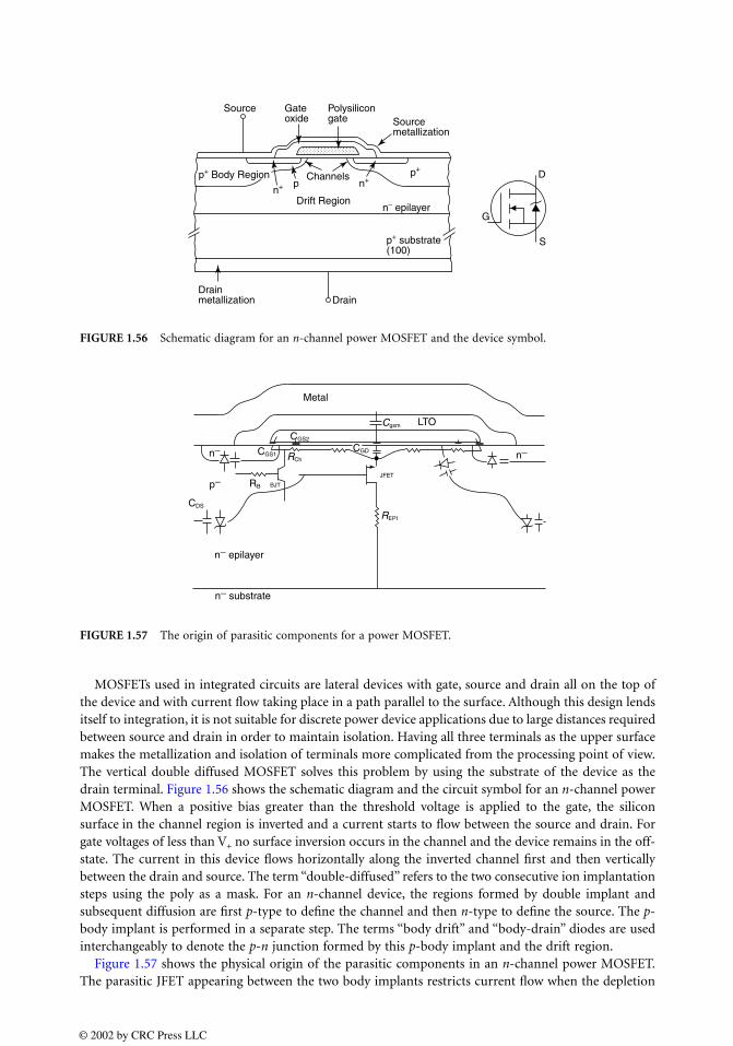
MOSFETs used in integrated circuits are lateral devices with gate, source and drain all on the top ofthe device and with current flow taking place in a path parallel to the surface. Although this design lendsitself to integration, it is not suitable for discrete power device applications due to large distances requiredbetween source and drain in order to maintain isolation. Having all three terminals as the upper surfacemakes the metallization and isolation of terminals more complicated from the processing point of view.The vertical double diffused MOSFET solves this problem by using the substrate of the device as thedrain terminal. Figure 1.56 shows the schematic diagram and the circuit symbol for an n-channel powerMOSFET. When a positive bias greater than the threshold voltage is applied to the gate, the siliconsurface in the channel region is inverted and a current starts to flow between the source and drain. Forgate voltages of less than V+ no surface inversion occurs in the channel and the device remains in the off-state. The current in this device flows horizontally along the inverted channel first and then verticallybetween the drain and source. The term “double-diffused” refers to the two consecutive ion implantationsteps using the poly as a mask. For an n-channel device, the regions formed by double implant andsubsequent diffusion are first p-type to define the channel and then n-type to define the source. The p-body implant is performed in a separate step. The terms “body drift” and “body-drain” diodes are usedinterchangeably to denote the p-n junction formed by this p-body implant and the drift region.
Figure 1.57 shows the physical origin of the parasitic components in an n-channel power MOSFET.The parasitic JFET appearing between the two body implants restricts current flow when the depletion
FIGURE 1.56 Schematic diagram for an n-channel power MOSFET and the device symbol.
FIGURE 1.57 The origin of parasitic components for a power MOSFET.
Source Gateoxide
Polysilicongate Source
metallization
p+ Body Region
p+ substrate(100)
n− epilayer
n+ n+p+
G
D
S
DrainDrainmetallization
Channelsp
Drift Region
Metal
LTOCGS2
CDS
p−
n− n−
n− epilayer
n− substrate
CGS1
RB
CGD
Cgsm
REPI
RCh
BJT
JFET
© 2002 by CRC Press LLC
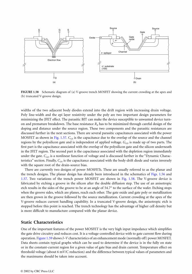
widths of the two adjacent body diodes extend into the drift region with increasing drain voltage.Poly line-width and the epi layer resistivity under the poly are two important design parameters forminimizing the JFET effect. The parasitic BJT can make the device susceptible to unwanted device turn-on and premature breakdown. The base resistance RB has to be minimized through careful design of thedoping and distance under the source region. These two components and the parasitic resistances arediscussed further in the next sections. There are several parasitic capacitances associated with the powerMOSFET as shown in Fig. 1.57. CGS is the capacitance due to the overlap of the source and the channelregions by the polysilicon gate and is independent of applied voltage. GGD is made up of two parts. Thefirst part is the capacitance associated with the overlap of the polysilicon gate and the silicon underneathin the JFET region. The second part is the capacitance associated with the depletion region immediatelyunder the gate. CGD is a nonlinear function of voltage and is discussed further in the “Dynamic Charac-teristics” section. Finally, CDS is the capacitance associated with the body-drift diode and varies inverselywith the square root of the drain-source bias.
There are currently two designs of power MOSFETs. These are usually referred to as the planar andthe trench designs. The planar design has already been introduced in the schematics of Figs. 1.56 and1.57. Two variations of the trench power MOSFET are shown in Fig. 1.58. The V-groove device isfabricated by etching a groove in the silicon after the double diffusion step. The use of an anisotropicetch results in the sides of the groove to be at an angle of 54.7° to the surface of the wafer. Etching stopswhen the groove sides, which are planes, reach each other. The gate oxide and gate poly or metallizationare then grown in the groove followed by the source metallization. Current crowding at the apex of theV-groove reduces current handling capability. In a truncated V-groove design, the anisotropic etch isstopped before this point is reached. The trench technology has the advantage of higher cell density butis more difficult to manufacture compared with the planar device.
Static Characteristics
One of the important features of the power MOSFET is the very high input impedance which simplifiesthe gate drive circuitry and reduces cost. It is a voltage-controlled device with to gate current flow duringoperation. Figure 1.59 shows I–V characteristics of an enhancement mode (normally off) power MOSFET.Data sheets contain typical graphs which can be used to determine if the device is in the fully on stateor in the constant-current region for a given value of gate bias and drain current. Temperature effect onthreshold voltage (about 6 mV/C reduction) and the difference between typical values of parameters andthe maximums should be taken into account.
FIGURE 1.58 Schematic diagram of (a) V-groove trench MOSFET showing the current crowding at the apex and(b) truncated V-groove design.
S G S
Electron flow
D
(a)
Source Source
Gateoxide
Gate
p
Oxide
Channel
Drain
n- epilayer
n+
n+ substrate(100)
(b)
© 2002 by CRC Press LLC
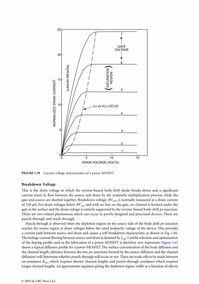
Breakdown Voltage
This is the drain voltage at which the reverse-biased body-drift diode breaks down and a significantcurrent starts to flow between the source and drain by the avalanche multiplication process, while thegate and source are shorted together. Breakdown voltage, BVDSS, is normally measured at a drain currentof 250 µA. For drain voltages below BVDSS and with no bias on the gate, no channel is formed under thegate at the surface and the drain voltage is entirely supported by the reverse-biased body-drift pn junction.There are two related phenomena which can occur in poorly designed and processed devices. These arepunch-through and reach-through.
Punch-through is observed when the depletion region on the source side of the body-drift pn-junctionreaches the source region at drain voltages below the rated avalanche voltage of the device. This providesa current path between source and drain and causes a soft breakdown characteristic as shown in Fig. 1.60.The leakage current flowing between source and drain is denoted by IDSS. Careful selection and optimizationof the doping profile used in the fabrication of a power MOSFET is therefore very important. Figure 1.61shows a typical diffusion profile for a power MOSFET. The surface concentration of the body diffusion andthe channel length (distance between the two pn-junctions formed by the source diffusion and the channeldiffusion) will determine whether punch-through will occur or not. There are trade-offs to be made betweenon-resistance Rdson which requires shorter channel lengths and punch-through avoidance which requireslonger channel lengths. An approximate equation giving the depletion region width as a function of silicon
FIGURE 1.59 Current-voltage characteristics of a power MOSFET.
0 5 10 15
DRAIN VOLTAGE (VOLTS)
1
2
3
4
IDS vs VDS LOCUS
5
GATEVOLTAGE
6
7
0
5
10
15
20
25
NO
RM
ALI
ZE
D D
RA
IN C
UR
RE
NT
(LIN
EA
R R
EG
ION
)
(SAT
UR
ATIO
N)
RE
GIO
N
© 2002 by CRC Press LLC
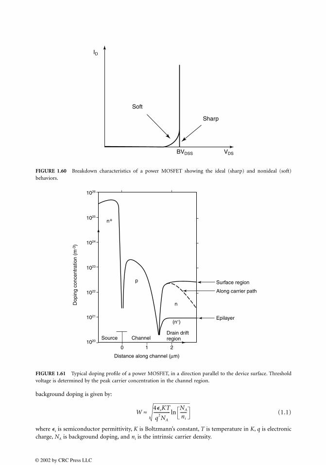
background doping is given by:
(1.1)
where s is semiconductor permittivity, K is Boltzmann’s constant, T is temperature in K, q is electroniccharge, NA is background doping, and ni is the intrinsic carrier density.
FIGURE 1.60 Breakdown characteristics of a power MOSFET showing the ideal (sharp) and nonideal (soft)behaviors.
FIGURE 1.61 Typical doping profile of a power MOSFET, in a direction parallel to the device surface. Thresholdvoltage is determined by the peak carrier concentration in the channel region.
ID
BVDSS VDS
Soft
Sharp
Source ChannelDrain driftregion
0 1 2
Distance along channel (µm)
Epilayer
Surface region
Along carrier path
(n-)
n+
1026
1025
1024
1023
1022
1021
1020
n
p
Dop
ing
conc
entr
atio
n (m
-3)
W4sKT
q2NA
---------------NA
ni
------ln≈
© 2002 by CRC Press LLC
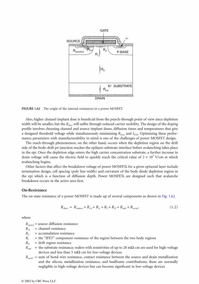
Also, higher channel implant dose is beneficial from the punch-through point of view since depletionwidth will be smaller, but the Rdson will suffer through reduced carrier mobility. The design of the dopingprofile involves choosing channel and source implant doses, diffusion times and temperatures that givea designed threshold voltage while simultaneously minimizing Rdson and IDSS. Optimizing these perfor-mance parameters with manufacturability in mind is one of the challenges of power MOSFET design.
The reach-through phenomenon, on the other hand, occurs when the depletion region on the driftside of the body-drift pn-junction reaches the epilayer-substrate interface before avalanching takes placein the epi. Once the depletion edge enters the high carrier concentration substrate, a further increase indrain voltage will cause the electric field to quickly reach the critical value of 2 × 10
5 V/cm at which
avalanching begins.Other factors that affect the breakdown voltage of power MOSFETs for a given epitaxial layer include
termination design, cell spacing (poly line width) and curvature of the body diode depletion region inthe epi which is a function of diffusion depth. Power MOSFETs are designed such that avalanchebreakdown occurs in the active area first.
On-Resistance
The on-state resistance of a power MOSFET is made up of several components as shown in Fig. 1.62.
(1.2)
where
Rsource = source diffusion resistanceRch = channel resistanceRA = accumulation resistanceRJ = the “JFET” component-resistance of the region between the two body regionsRD = drift region resistanceRsub = the substrate resistance; wafers with resistivities of up to 20 mΩ-cm are used for high-voltage
devices and less than 5 mΩ-cm for low-voltage devicesRwcml = sum of bond wire resistance, contact resistance between the source and drain metallization
and the silicon, metallization resistance, and leadframe contributions; these are normallynegligible in high-voltage devices but can become significant in low-voltage devices
FIGURE 1.62 The origin of the internal resistances in a power MOSFET.
SOURCE
GATE
N+ SUBSTRATE
DRAIN
Rsub
RSOURCERCH
RJ
RA P-BASE
N+
RD
Rdson Rsource Rch RA RJ RD Rsub Rwcml+ + + + + +=
© 2002 by CRC Press LLC
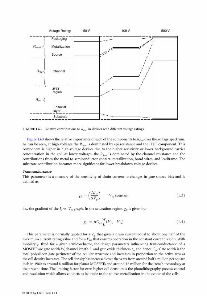
Figure 1.63 shows the relative importance of each of the components to Rdson over the voltage spectrum.As can be seen, at high voltages the Rdson is dominated by epi resistance and the JFET component. Thiscomponent is higher in high-voltage devices due to the higher resistivity or lower background carrierconcentration in the epi. At lower voltages, the Rdson is dominated by the channel resistance and thecontributions from the metal to semiconductor contact, metallization, bond wires, and leadframe. Thesubstrate contribution becomes more significant for lower breakdown voltage devices.
TransconductanceThis parameter is a measure of the sensitivity of drain current to changes in gate-source bias and isdefined as:
(1.3)
i.e., the gradient of the Id vs. Vgs graph. In the saturation region, gfs is given by:
(1.4)
This parameter is normally quoted for a Vgs that gives a drain current equal to about one half of themaximum current rating value and for a VDS that ensures operation in the constant current region. Withmobility µ fixed for a given semiconductor, the design parameters influencing transconductance of aMOSFET are gate width W, channel length L, and gate oxide thickness tox and hence Cox. Gate width is thetotal polysilicon gate perimeter of the cellular structure and increases in proportion to the active area asthe cell density increases. The cell density has increased over the years from around half a million per squareinch in 1980 to around 8 million for planar MOSFETs and around 12 million for the trench technology atthe present time. The limiting factor for even higher cell densities is the photolithography process controland resolution which allows contacts to be made to the source metallization in the center of the cells.
FIGURE 1.63 Relative contributions to Rdson in devices with different voltage ratings.
Voltage Rating:
Packaging
Metallization
Source
Channel
JFETregion
Epitaxiallayer
Substrate
50 V 100 V 500 V
Rwcml
RCh
REPI
gfs
∆ID
∆Vgs
----------- Vds constant=
gfs µCoxWL----- Vgs Vth–( )=
© 2002 by CRC Press LLC
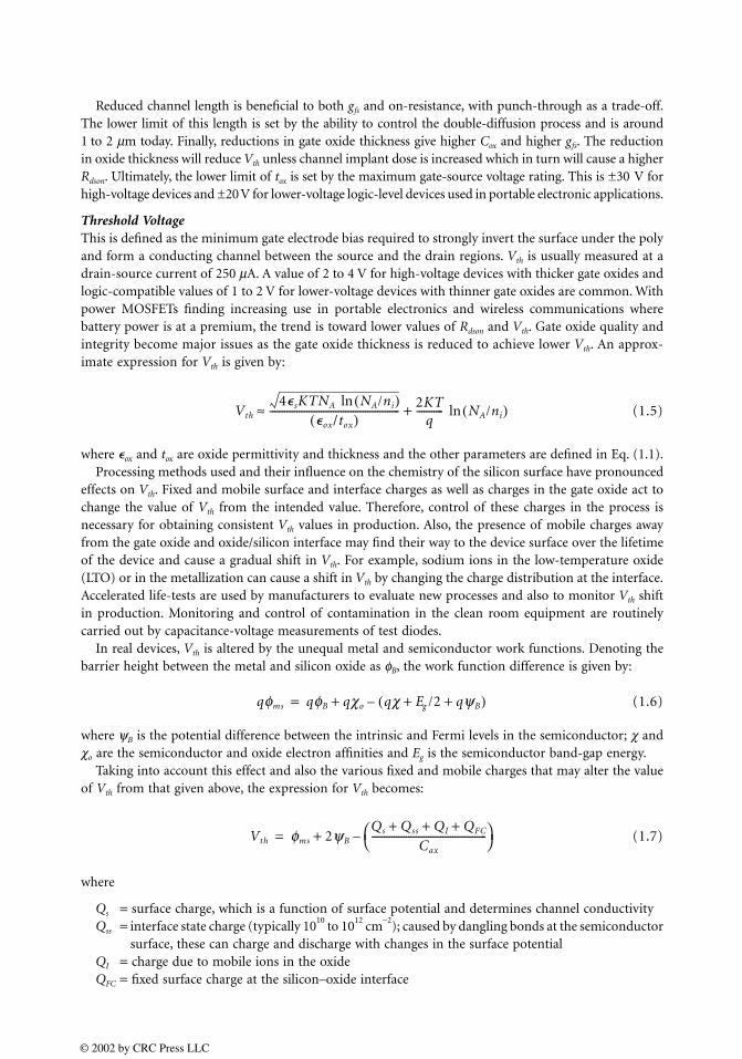
Reduced channel length is beneficial to both gfs and on-resistance, with punch-through as a trade-off.The lower limit of this length is set by the ability to control the double-diffusion process and is around1 to 2 µm today. Finally, reductions in gate oxide thickness give higher Cox and higher gfs. The reductionin oxide thickness will reduce Vth unless channel implant dose is increased which in turn will cause a higherRdson. Ultimately, the lower limit of tox is set by the maximum gate-source voltage rating. This is ±30 V forhigh-voltage devices and ±20 V for lower-voltage logic-level devices used in portable electronic applications.
Threshold VoltageThis is defined as the minimum gate electrode bias required to strongly invert the surface under the polyand form a conducting channel between the source and the drain regions. Vth is usually measured at adrain-source current of 250 µA. A value of 2 to 4 V for high-voltage devices with thicker gate oxides andlogic-compatible values of 1 to 2 V for lower-voltage devices with thinner gate oxides are common. Withpower MOSFETs finding increasing use in portable electronics and wireless communications wherebattery power is at a premium, the trend is toward lower values of Rdson and Vth. Gate oxide quality andintegrity become major issues as the gate oxide thickness is reduced to achieve lower Vth. An approx-imate expression for Vth is given by:
(1.5)
where ox and tox are oxide permittivity and thickness and the other parameters are defined in Eq. (1.1).Processing methods used and their influence on the chemistry of the silicon surface have pronounced
effects on Vth. Fixed and mobile surface and interface charges as well as charges in the gate oxide act tochange the value of Vth from the intended value. Therefore, control of these charges in the process isnecessary for obtaining consistent Vth values in production. Also, the presence of mobile charges awayfrom the gate oxide and oxide/silicon interface may find their way to the device surface over the lifetimeof the device and cause a gradual shift in Vth. For example, sodium ions in the low-temperature oxide(LTO) or in the metallization can cause a shift in Vth by changing the charge distribution at the interface.Accelerated life-tests are used by manufacturers to evaluate new processes and also to monitor Vth shiftin production. Monitoring and control of contamination in the clean room equipment are routinelycarried out by capacitance-voltage measurements of test diodes.
In real devices, Vth is altered by the unequal metal and semiconductor work functions. Denoting thebarrier height between the metal and silicon oxide as φB, the work function difference is given by:
(1.6)
where ψB is the potential difference between the intrinsic and Fermi levels in the semiconductor; χ andχo are the semiconductor and oxide electron affinities and Eg is the semiconductor band-gap energy.
Taking into account this effect and also the various fixed and mobile charges that may alter the valueof Vth from that given above, the expression for Vth becomes:
(1.7)
where
Qs = surface charge, which is a function of surface potential and determines channel conductivityQss = interface state charge (typically 10
10 to 10
12 cm
−2); caused by dangling bonds at the semiconductor
surface, these can charge and discharge with changes in the surface potentialQI = charge due to mobile ions in the oxideQFC = fixed surface charge at the silicon–oxide interface
Vth
4sKTNA NA/ni( )lnox/tox( )
----------------------------------------------------- 2KTq
----------- NA/ni( )ln+≈
qφms qφB qχo qχ Eg /2 qψB+ +( )–+=
Vth φms 2ψB
Qs Qss QI QFC+ + +Cax
----------------------------------------------- –+=
© 2002 by CRC Press LLC
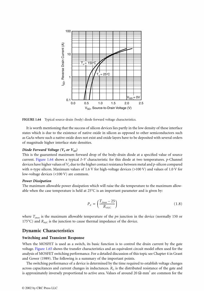
It is worth mentioning that the success of silicon devices lies partly in the low density of these interfacestates which is due to the existence of native oxide in silicon as opposed to other semiconductors suchas GaAs where such a native oxide does not exist and oxide layers have to be deposited with several ordersof magnitude higher interface state densities.
Diode Forward Voltage (VF or VSD)This is the guaranteed maximum forward drop of the body-drain diode at a specified value of sourcecurrent. Figure 1.64 shows a typical I–V characteristic for this diode at two temperatures. p-Channeldevices have higher values of VF due to the higher contact resistance between metal and p-silicon comparedwith n-type silicon. Maximum values of 1.6 V for high-voltage devices (>100 V) and values of 1.0 V forlow-voltage devices (<100 V) are common.
Power DissipationThe maximum allowable power dissipation which will raise the die temperature to the maximum allow-able when the case temperature is held at 25°C is an important parameter and is given by:
(1.8)
where Tjmax is the maximum allowable temperature of the pn junction in the device (normally 150 or175°C) and RthJC is the junction to cause thermal impedance of the device.
Dynamic Characteristics
Switching and Transient Response
When the MOSFET is used as a switch, its basic function is to control the drain current by the gatevoltage. Figure 1.65 shows the transfer characteristics and an equivalent circuit model often used for theanalysis of MOSFET switching performance. For a detailed discussion of this topic see Chapter 4 in Grantand Gower (1989). The following is a summary of the important points.
The switching performance of a device is determined by the time required to establish voltage changesacross capacitances and current changes in inductances. RG is the distributed resistance of the gate andis approximately inversely proportional to active area. Values of around 20 Ω-mm
2 are common for the
FIGURE 1.64 Typical source-drain (body) diode forward voltage characteristics.
100
10
1
0.10.0 0.5 1.0 1.5 2.0 2.5
VSD, Source-to-Drain Voltage (V)
I SD, R
ever
se D
rain
Cur
rent
(A
)
VGS = 0V
TJ = 25oC
TJ = 150oC
Pd
Tjmax 25–RthJC
----------------------- =
© 2002 by CRC Press LLC
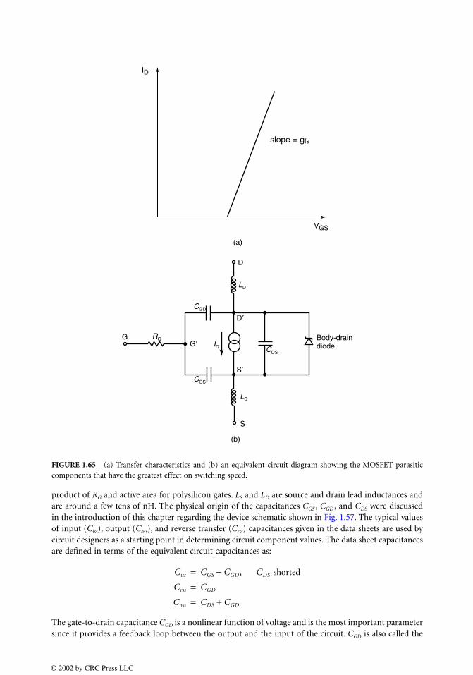
product of RG and active area for polysilicon gates. LS and LD are source and drain lead inductances andare around a few tens of nH. The physical origin of the capacitances CGS , CGD , and CDS were discussedin the introduction of this chapter regarding the device schematic shown in Fig. 1.57. The typical valuesof input (Ciss), output (Coss), and reverse transfer (Crss) capacitances given in the data sheets are used bycircuit designers as a starting point in determining circuit component values. The data sheet capacitancesare defined in terms of the equivalent circuit capacitances as:
The gate-to-drain capacitance CGD is a nonlinear function of voltage and is the most important parametersince it provides a feedback loop between the output and the input of the circuit. CGD is also called the
FIGURE 1.65 (a) Transfer characteristics and (b) an equivalent circuit diagram showing the MOSFET parasiticcomponents that have the greatest effect on switching speed.
ID
VGS
LD
ID
LS
CGD
CDS
CGS
RG
slope = gfs
(a)
(b)
D
G′G Body-drain
diode
D′
S′
S
Ciss CGS CGD, CDS shorted+=Crss CGD=Coss CDS CGD+=
© 2002 by CRC Press LLC
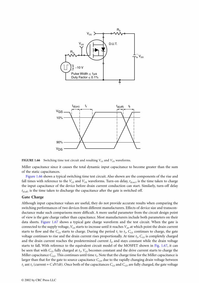
Miller capacitance since it causes the total dynamic input capacitance to become greater than the sumof the static capacitances.
Figure 1.66 shows a typical switching time test circuit. Also shown are the components of the rise andfall times with reference to the VGS and VDS waveforms. Turn-on delay, td(on), is the time taken to chargethe input capacitance of the device before drain current conduction can start. Similarly, turn-off delaytd(off) is the time taken to discharge the capacitance after the gate is switched off.
Gate Charge
Although input capacitance values are useful, they do not provide accurate results when comparing theswitching performances of two devices from different manufacturers. Effects of device size and transcon-ductance make such comparisons more difficult. A more useful parameter from the circuit design pointof view is the gate charge rather than capacitance. Most manufacturers include both parameters on theirdata sheets. Figure 1.67 shows a typical gate charge waveform and the test circuit. When the gate isconnected to the supply voltage, VGS starts to increase until it reaches Vth, at which point the drain currentstarts to flow and the CGS starts to charge. During the period t1 to t2, CGS continues to charge, the gatevoltage continues to rise and the drain current rises proportionally. At time t2, CGS is completely chargedand the drain current reaches the predetermined current ID and stays constant while the drain voltagestarts to fall. With reference to the equivalent circuit model of the MOSFET shown in Fig. 1.67, it canbe seen that with CGS fully charged at t2, VGS becomes constant and the drive current starts to charge theMiller capacitance CGD. This continues until time t3. Note that the charge time for the Miller capacitance islarger than that for the gate to source capacitance CGS, due to the rapidly changing drain voltage betweent2 ant t3 (current = C dV/dt). Once both of the capacitances CGS and CGD are fully charged, the gate voltage
FIGURE 1.66 Switching time test circuit and resulting VGS and VDS waveforms.
td(on) tr
RG
−10 V
Pulse Width <_ 1µsDuty Factor <_ 0.1%
VGS
VDS
RD
VDD
td(off) tfVGS
VDS
10%
90%
D.U.T.
−+
© 2002 by CRC Press LLC
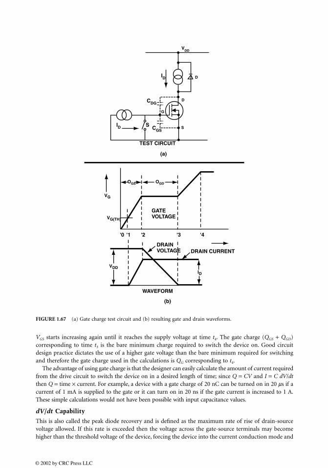
VGS starts increasing again until it reaches the supply voltage at time t4. The gate charge (QGS + QGD)corresponding to time t3 is the bare minimum charge required to switch the device on. Good circuitdesign practice dictates the use of a higher gate voltage than the bare minimum required for switchingand therefore the gate charge used in the calculations is QG corresponding to t4.
The advantage of using gate charge is that the designer can easily calculate the amount of current requiredfrom the drive circuit to switch the device on in a desired length of time; since Q = CV and I = C dV/dtthen Q = time × current. For example, a device with a gate charge of 20 nC can be turned on in 20 µs if acurrent of 1 mA is supplied to the gate or it can turn on in 20 ns if the gate current is increased to 1 A.These simple calculations would not have been possible with input capacitance values.
dV/dt Capability
This is also called the peak diode recovery and is defined as the maximum rate of rise of drain-sourcevoltage allowed. If this rate is exceeded then the voltage across the gate-source terminals may becomehigher than the threshold voltage of the device, forcing the device into the current conduction mode and
FIGURE 1.67 (a) Gate charge test circuit and (b) resulting gate and drain waveforms.
VDD
ID
ID
TEST CIRCUIT
CDG
CGS
OGDOGS
VG
VG(TH)
VDDID
'0 '1 '2 '3 '4
SS
D
G
D
(a)
(b)
GATEVOLTAGE
DRAINVOLTAGE DRAIN CURRENT
WAVEFORM
© 2002 by CRC Press LLC
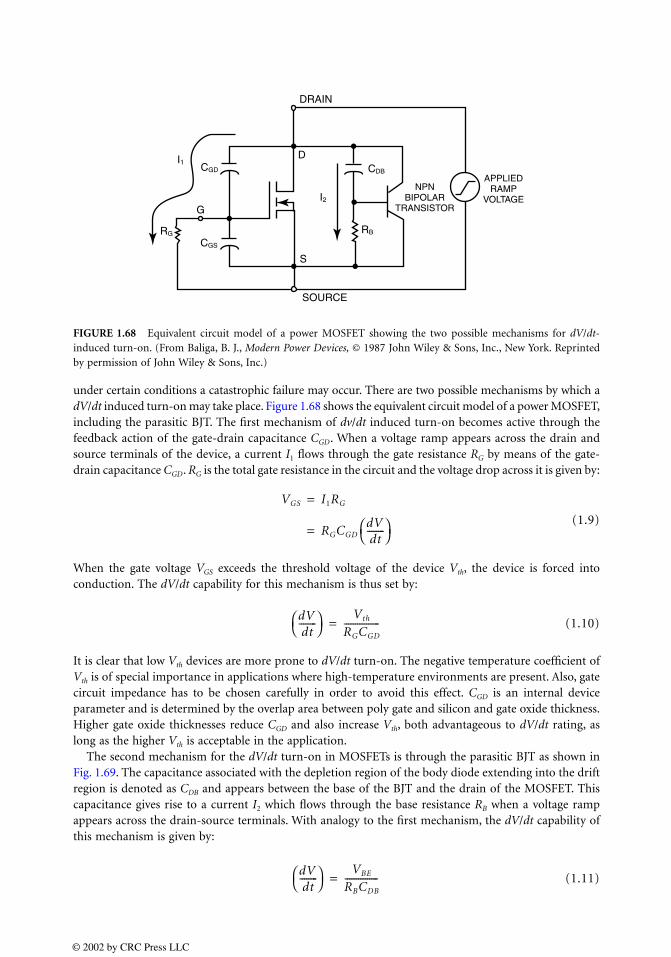
under certain conditions a catastrophic failure may occur. There are two possible mechanisms by which adV/dt induced turn-on may take place. Figure 1.68 shows the equivalent circuit model of a power MOSFET,including the parasitic BJT. The first mechanism of dv/dt induced turn-on becomes active through thefeedback action of the gate-drain capacitance CGD. When a voltage ramp appears across the drain andsource terminals of the device, a current I1 flows through the gate resistance RG by means of the gate-drain capacitance CGD. RG is the total gate resistance in the circuit and the voltage drop across it is given by:
(1.9)
When the gate voltage VGS exceeds the threshold voltage of the device Vth, the device is forced intoconduction. The dV/dt capability for this mechanism is thus set by:
(1.10)
It is clear that low Vth devices are more prone to dV/dt turn-on. The negative temperature coefficient ofVth is of special importance in applications where high-temperature environments are present. Also, gatecircuit impedance has to be chosen carefully in order to avoid this effect. CGD is an internal deviceparameter and is determined by the overlap area between poly gate and silicon and gate oxide thickness.Higher gate oxide thicknesses reduce CGD and also increase Vth, both advantageous to dV/dt rating, aslong as the higher Vth is acceptable in the application.
The second mechanism for the dV/dt turn-on in MOSFETs is through the parasitic BJT as shown inFig. 1.69. The capacitance associated with the depletion region of the body diode extending into the driftregion is denoted as CDB and appears between the base of the BJT and the drain of the MOSFET. Thiscapacitance gives rise to a current I2 which flows through the base resistance RB when a voltage rampappears across the drain-source terminals. With analogy to the first mechanism, the dV/dt capability ofthis mechanism is given by:
(1.11)
FIGURE 1.68 Equivalent circuit model of a power MOSFET showing the two possible mechanisms for dV/dt-induced turn-on. (From Baliga, B. J., Modern Power Devices, © 1987 John Wiley & Sons, Inc., New York. Reprintedby permission of John Wiley & Sons, Inc.)
DRAIN
SOURCE
D
S
I1
I2
CGD CDB
RB
CGS
RG
G
NPNBIPOLAR
TRANSISTOR
APPLIEDRAMP
VOLTAGE
VGS I1RG=
RGCGDdVdt--------
=
dVdt--------
Vth
RGCGD
----------------=
dVdt--------
VBE
RBCDB
---------------=
© 2002 by CRC Press LLC

If the voltage that develops across RB is greater than about 0.7 V, then the base–emitter junction is forward-biased and the parasitic BJT is turned on. Under the conditions of high dV/dt and large values of RB, the break-down voltage of the MOSFET will be limited to that of the open-base breakdown voltage of the BJT. Ifthe applied drain voltage is greater than the open-base breakdown voltage, then the MOSFET will enteravalanche and may be destroyed if the current is not limited externally.
Increasing dV/dt capability therefore requires reducing the base resistance RB by increasing the bodyregion doping and reducing the distance the current I2 has to flow laterally before it is collected by thesource metallization. As in the first mode, the BJT related dV/dt capability becomes worse at highertemperatures since RB increases and VBE decreases with increasing temperature.
Applications
The following are two of the major markets where power MOSFETs are finding increasing applicationsas either logic-controlled or analog switches.
Portable Electronics and Wireless Communication
With the recent advances in the portable electronic products, low Rdson, logic level surface mount powerMOSFET are experiencing explosive demand. A portable computer, for example, uses power MOSFETsin the AC-DC converters, the DC-DC converters and voltage regulators, load management switches,battery charger circuitry, and reverse battery protection. Required features of MOSFETs in these appli-cations are small size, low power dissipation, and low on-resistance for extended battery life. Reductionof both conduction and switching losses are important considerations in the design of MOSFETs aimedat this market.
Automotive
Mechanical contact breakers have mostly been replaced by semiconductor devices in ignition circuits inmodern cars. A suitable semiconductor device must be capable of blocking high voltages in a severeenvironment where line voltage surges are common due to the opening and closing of switches and theconnection and disconnection of inductive loads during maintenance and loose connections. Bipolartransistors with their susceptibility to secondary breakdown are not suited whereas power MOSFETs withavalanche capability are ideally suited. Voltage transients are clamped by the avalanching of the MOSFETwithout the need to use any external protection circuits.
FIGURE 1.69 Physical origin of the parasitic BJT components that may cause dV/dt-induced turn-on in powerMOSFET. (From Baliga, B. J., Modern Power Devices, © 1987 John Wiley & Sons, Inc., New York. Reprinted bypermission of John Wiley & Sons, Inc.)
SOURCE
N+
LN+
RS
CDB
A
DRAIN
GATE
© 2002 by CRC Press LLC

In 12-V battery vehicles the most commonly used MOSFETs are rated at 50 or 60 V breakdown volt-ages. The significant guard-banding is necessary in order to avoid device failure due to the alternatorproducing high voltages after shedding a heavy load.
The other features of power MOSFETs which make them suitable for the automotive applications are highdV/dt ratings, high-temperature performance, ruggedness and high reliability. Logic level, surface mountdevices with low Rdson have recently found application in this field. The smaller footprint of surface mountsoffers space savings and the lower Rdson does away with the need to parallel devices to reduce on-resistance.This in turn translates into fewer device counts and heat-sinks which lowers the overall cost.
In addition to ignition control, power MOSFETs are used in anti-lock brake (ABS) systems, electronicpower steering (EPS) systems, air bags, electronic suspension, and numerous motor control applicationssuch as power windows, power seats, radiator fan, wipers, fuel pump, etc.
References
Baliga, B.J. 1987. Modern Power Devices, John Wiley & Sons, New York.Grant, D.A. and Gower, I. 1989. Power MOSFETs—Theory and Applications, John Wiley & Sons, New York.International Rectifier, 1995, HEXFET Power MOSFET Designer’s Manual—Application Notes and Reli-
ability Data, International Rectifier, El Segundo, CA.Oxner, E.S. 1982. Power FETs and Their Applications, Prentice-Hall, Englewood Cliffs, NJ.Sze, S.M. 1981. Physics of Semiconductor Devices, John Wiley & Sons, New York.
1.7 General Power Semiconductor Switch Requirements
Alex Q. Huang
A power semiconductor switch is a component that can either conduct a current when it is commandedON or block a voltage when it is commanded OFF through a control. This change of conductivity ismade possible in a semiconductor by specially arranged device structures that control the carrier trans-portation. The time that it takes to change the conductivity is also reduced to the microsecond levelcompared with the millisecond level of a mechanical switch. By employing this kind of switch, a properlydesigned electrical system can control the flow of electric energy, shaping the electricity into desiredforms.
Parameters describing the performance of a power conversion system include reliability, efficiency,size, and cost. The power switch plays an important role in determining these system-level performances[1]. To facilitate the analysis, a simple buck converter shown in Fig. 1.70a (buck converter) and 1.70b(its switching waveforms) is used as an example. There are two switches SW and DF in the circuit. Thepurpose of this circuit is to deliver energy from a power source with a higher voltage VCC to the loadwith a lower voltage VO requirement. When the power switch SW is on, the energy is delivered from thesource VCC through switch SW, inductor L to the load. When the output voltage is high enough, thisenergy link will be shut down by turning off SW. Energies stored in L and CO will maintain the loadvoltage. The typical circuit waveforms are depicted in Figs. 1.70a and b its switching waveforms. Thecircuit has four different operating modes: (1) (t0–t1) SW off and DF on; (2) (t1–t3) SW turn-on and DF
turn-off; (3) (t3–t4) SW on and DF off; (4) (t4–t6) SW turn-off and DF turn-on.Generally, the following parameters are important for a semiconductor switch designed for power
conversion applications:
1. Maximum current carrying capability2. Maximum voltage blocking capability3. Forward voltage drop during ON and its temperature dependency4. Leakage current during OFF5. Thermal capability
© 2002 by CRC Press LLC
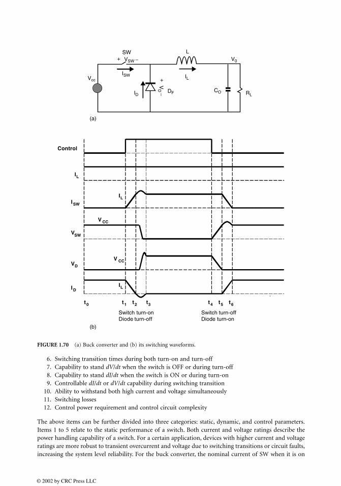
6. Switching transition times during both turn-on and turn-off7. Capability to stand dV/dt when the switch is OFF or during turn-off8. Capability to stand dI/dt when the switch is ON or during turn-on9. Controllable dI/dt or dV/dt capability during switching transition
10. Ability to withstand both high current and voltage simultaneously11. Switching losses12. Control power requirement and control circuit complexity
The above items can be further divided into three categories: static, dynamic, and control parameters.Items 1 to 5 relate to the static performance of a switch. Both current and voltage ratings describe thepower handling capability of a switch. For a certain application, devices with higher current and voltageratings are more robust to transient overcurrent and voltage due to switching transitions or circuit faults,increasing the system level reliability. For the buck converter, the nominal current of SW when it is on
FIGURE 1.70 (a) Buck converter and (b) its switching waveforms.
Control
IL
ISW
VSW
VD
ID
V CC
t1
IL
IL
V CC
t2 t3 t4 t5 t6
Switch turn-onDiode turn-off
Switch turn-offDiode turn-on
t0
(a)
(b)
Vcc
SWVSW
ISW
ID
LV0
IL
DF CO RL
VD
+
+ −
−
© 2002 by CRC Press LLC
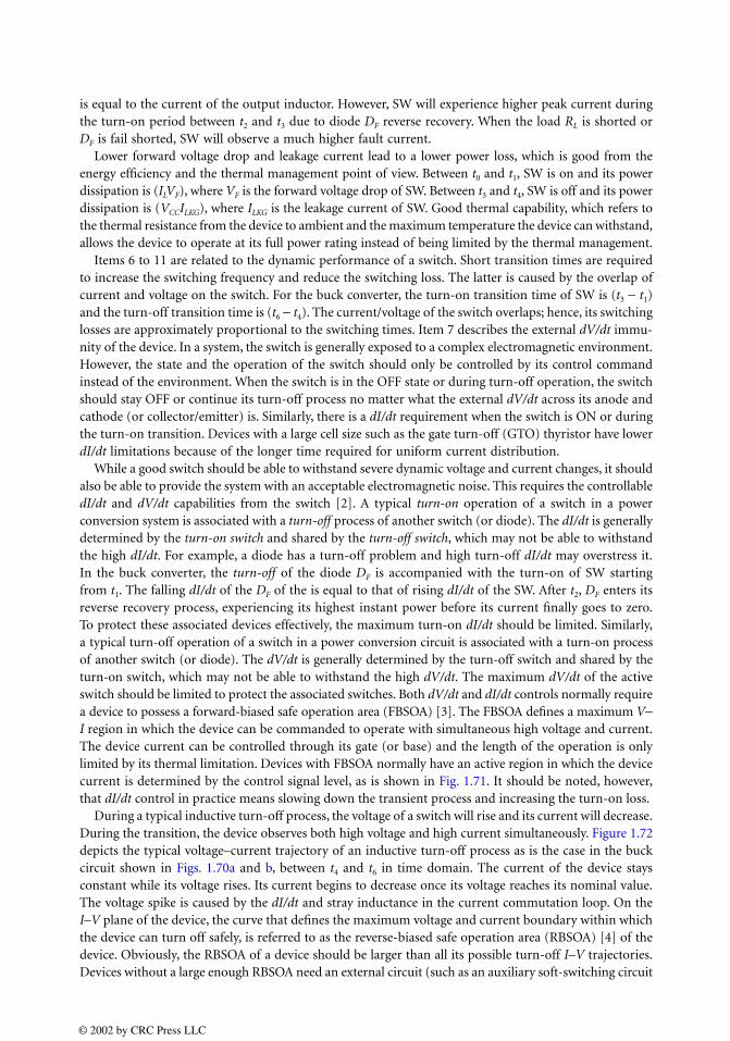
is equal to the current of the output inductor. However, SW will experience higher peak current duringthe turn-on period between t2 and t3 due to diode DF reverse recovery. When the load RL is shorted orDF is fail shorted, SW will observe a much higher fault current.
Lower forward voltage drop and leakage current lead to a lower power loss, which is good from theenergy efficiency and the thermal management point of view. Between t0 and t1, SW is on and its powerdissipation is (ILVF), where VF is the forward voltage drop of SW. Between t3 and t4, SW is off and its powerdissipation is (VCCILKG), where ILKG is the leakage current of SW. Good thermal capability, which refers tothe thermal resistance from the device to ambient and the maximum temperature the device can withstand,allows the device to operate at its full power rating instead of being limited by the thermal management.
Items 6 to 11 are related to the dynamic performance of a switch. Short transition times are requiredto increase the switching frequency and reduce the switching loss. The latter is caused by the overlap ofcurrent and voltage on the switch. For the buck converter, the turn-on transition time of SW is (t3 − t1)and the turn-off transition time is (t6 − t4). The current/voltage of the switch overlaps; hence, its switchinglosses are approximately proportional to the switching times. Item 7 describes the external dV/dt immu-nity of the device. In a system, the switch is generally exposed to a complex electromagnetic environment.However, the state and the operation of the switch should only be controlled by its control commandinstead of the environment. When the switch is in the OFF state or during turn-off operation, the switchshould stay OFF or continue its turn-off process no matter what the external dV/dt across its anode andcathode (or collector/emitter) is. Similarly, there is a dI/dt requirement when the switch is ON or duringthe turn-on transition. Devices with a large cell size such as the gate turn-off (GTO) thyristor have lowerdI/dt limitations because of the longer time required for uniform current distribution.
While a good switch should be able to withstand severe dynamic voltage and current changes, it shouldalso be able to provide the system with an acceptable electromagnetic noise. This requires the controllabledI/dt and dV/dt capabilities from the switch [2]. A typical turn-on operation of a switch in a powerconversion system is associated with a turn-off process of another switch (or diode). The dI/dt is generallydetermined by the turn-on switch and shared by the turn-off switch, which may not be able to withstandthe high dI/dt. For example, a diode has a turn-off problem and high turn-off dI/dt may overstress it.In the buck converter, the turn-off of the diode DF is accompanied with the turn-on of SW startingfrom t1. The falling dI/dt of the DF of the is equal to that of rising dI/dt of the SW. After t2, DF enters itsreverse recovery process, experiencing its highest instant power before its current finally goes to zero.To protect these associated devices effectively, the maximum turn-on dI/dt should be limited. Similarly,a typical turn-off operation of a switch in a power conversion circuit is associated with a turn-on processof another switch (or diode). The dV/dt is generally determined by the turn-off switch and shared by theturn-on switch, which may not be able to withstand the high dV/dt. The maximum dV/dt of the activeswitch should be limited to protect the associated switches. Both dV/dt and dI/dt controls normally requirea device to possess a forward-biased safe operation area (FBSOA) [3]. The FBSOA defines a maximum V−I region in which the device can be commanded to operate with simultaneous high voltage and current.The device current can be controlled through its gate (or base) and the length of the operation is onlylimited by its thermal limitation. Devices with FBSOA normally have an active region in which the devicecurrent is determined by the control signal level, as is shown in Fig. 1.71. It should be noted, however,that dI/dt control in practice means slowing down the transient process and increasing the turn-on loss.
During a typical inductive turn-off process, the voltage of a switch will rise and its current will decrease.During the transition, the device observes both high voltage and high current simultaneously. Figure 1.72depicts the typical voltage–current trajectory of an inductive turn-off process as is the case in the buckcircuit shown in Figs. 1.70a and b, between t4 and t6 in time domain. The current of the device staysconstant while its voltage rises. Its current begins to decrease once its voltage reaches its nominal value.The voltage spike is caused by the dI/dt and stray inductance in the current commutation loop. On theI–V plane of the device, the curve that defines the maximum voltage and current boundary within whichthe device can turn off safely, is referred to as the reverse-biased safe operation area (RBSOA) [4] of thedevice. Obviously, the RBSOA of a device should be larger than all its possible turn-off I–V trajectories.Devices without a large enough RBSOA need an external circuit (such as an auxiliary soft-switching circuit
© 2002 by CRC Press LLC
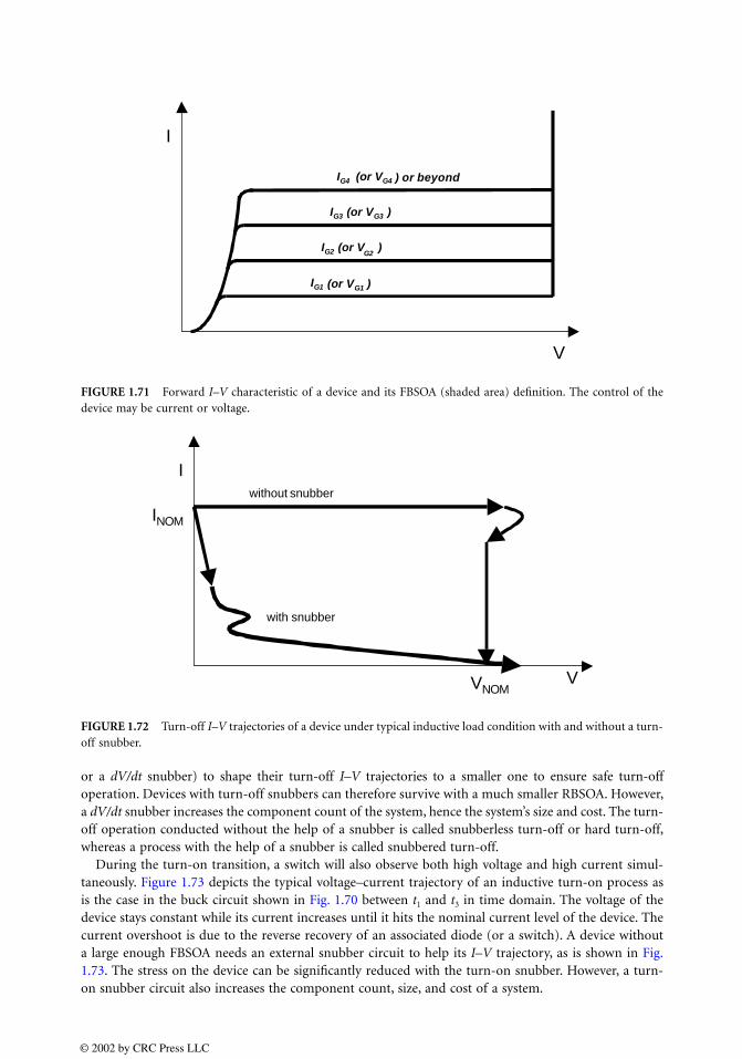
or a dV/dt snubber) to shape their turn-off I–V trajectories to a smaller one to ensure safe turn-offoperation. Devices with turn-off snubbers can therefore survive with a much smaller RBSOA. However,a dV/dt snubber increases the component count of the system, hence the system’s size and cost. The turn-off operation conducted without the help of a snubber is called snubberless turn-off or hard turn-off,whereas a process with the help of a snubber is called snubbered turn-off.
During the turn-on transition, a switch will also observe both high voltage and high current simul-taneously. Figure 1.73 depicts the typical voltage–current trajectory of an inductive turn-on process asis the case in the buck circuit shown in Fig. 1.70 between t1 and t3 in time domain. The voltage of thedevice stays constant while its current increases until it hits the nominal current level of the device. Thecurrent overshoot is due to the reverse recovery of an associated diode (or a switch). A device withouta large enough FBSOA needs an external snubber circuit to help its I–V trajectory, as is shown in Fig.1.73. The stress on the device can be significantly reduced with the turn-on snubber. However, a turn-on snubber circuit also increases the component count, size, and cost of a system.
FIGURE 1.71 Forward I–V characteristic of a device and its FBSOA (shaded area) definition. The control of thedevice may be current or voltage.
FIGURE 1.72 Turn-off I–V trajectories of a device under typical inductive load condition with and without a turn-off snubber.
V
I
IG1 (or VG1 )
IG2 (or VG2
)
IG3 (or VG3 )
IG4 (or VG4 ) or beyond
V
I
VNOM
INOM
without snubber
with snubber
© 2002 by CRC Press LLC
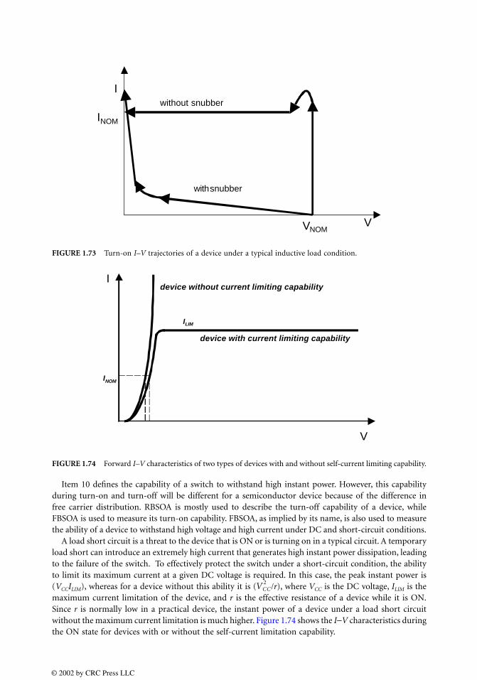
Item 10 defines the capability of a switch to withstand high instant power. However, this capabilityduring turn-on and turn-off will be different for a semiconductor device because of the difference infree carrier distribution. RBSOA is mostly used to describe the turn-off capability of a device, whileFBSOA is used to measure its turn-on capability. FBSOA, as implied by its name, is also used to measurethe ability of a device to withstand high voltage and high current under DC and short-circuit conditions.
A load short circuit is a threat to the device that is ON or is turning on in a typical circuit. A temporaryload short can introduce an extremely high current that generates high instant power dissipation, leadingto the failure of the switch. To effectively protect the switch under a short-circuit condition, the abilityto limit its maximum current at a given DC voltage is required. In this case, the peak instant power is(VCCILIM), whereas for a device without this ability it is ( /r), where VCC is the DC voltage, ILIM is themaximum current limitation of the device, and r is the effective resistance of a device while it is ON.Since r is normally low in a practical device, the instant power of a device under a load short circuitwithout the maximum current limitation is much higher. Figure 1.74 shows the I−V characteristics duringthe ON state for devices with or without the self-current limitation capability.
FIGURE 1.73 Turn-on I–V trajectories of a device under a typical inductive load condition.
FIGURE 1.74 Forward I–V characteristics of two types of devices with and without self-current limiting capability.
V
I
VNOM
INOM
without snubber
with snubber
V
I
ILIM
device without current limiting capability
device with current limiting capability
INOM
VCC2
© 2002 by CRC Press LLC
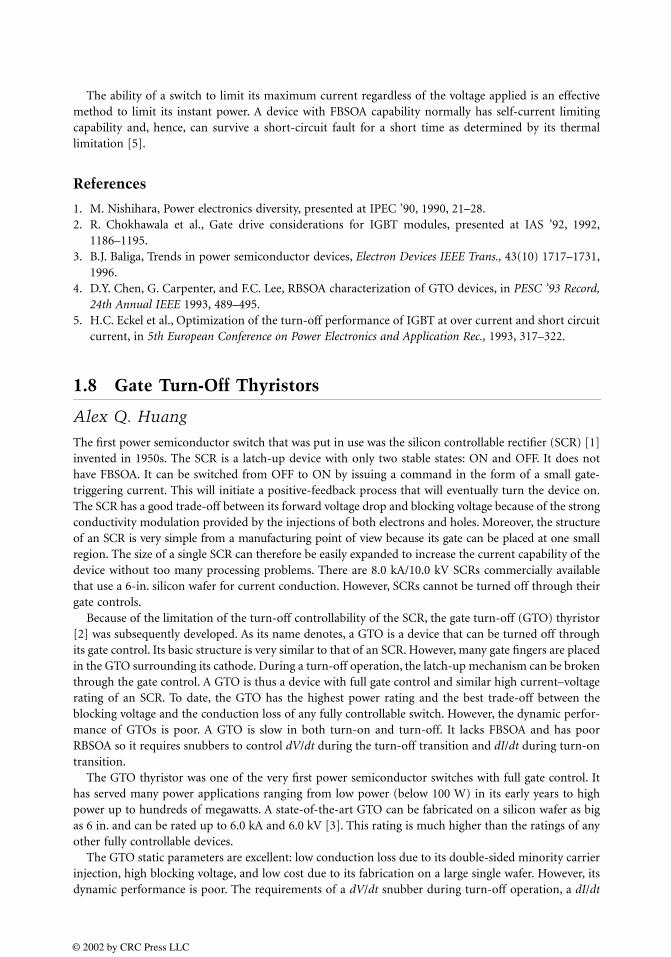
The ability of a switch to limit its maximum current regardless of the voltage applied is an effectivemethod to limit its instant power. A device with FBSOA capability normally has self-current limitingcapability and, hence, can survive a short-circuit fault for a short time as determined by its thermallimitation [5].
References
1. M. Nishihara, Power electronics diversity, presented at IPEC ’90, 1990, 21–28.2. R. Chokhawala et al., Gate drive considerations for IGBT modules, presented at IAS ’92, 1992,
1186–1195.3. B.J. Baliga, Trends in power semiconductor devices, Electron Devices IEEE Trans., 43(10) 1717–1731,
1996.4. D.Y. Chen, G. Carpenter, and F.C. Lee, RBSOA characterization of GTO devices, in PESC ’93 Record,
24th Annual IEEE 1993, 489–495.5. H.C. Eckel et al., Optimization of the turn-off performance of IGBT at over current and short circuit
current, in 5th European Conference on Power Electronics and Application Rec., 1993, 317–322.
1.8 Gate Turn-Off Thyristors
Alex Q. Huang
The first power semiconductor switch that was put in use was the silicon controllable rectifier (SCR) [1]invented in 1950s. The SCR is a latch-up device with only two stable states: ON and OFF. It does nothave FBSOA. It can be switched from OFF to ON by issuing a command in the form of a small gate-triggering current. This will initiate a positive-feedback process that will eventually turn the device on.The SCR has a good trade-off between its forward voltage drop and blocking voltage because of the strongconductivity modulation provided by the injections of both electrons and holes. Moreover, the structureof an SCR is very simple from a manufacturing point of view because its gate can be placed at one smallregion. The size of a single SCR can therefore be easily expanded to increase the current capability of thedevice without too many processing problems. There are 8.0 kA/10.0 kV SCRs commercially availablethat use a 6-in. silicon wafer for current conduction. However, SCRs cannot be turned off through theirgate controls.
Because of the limitation of the turn-off controllability of the SCR, the gate turn-off (GTO) thyristor[2] was subsequently developed. As its name denotes, a GTO is a device that can be turned off throughits gate control. Its basic structure is very similar to that of an SCR. However, many gate fingers are placedin the GTO surrounding its cathode. During a turn-off operation, the latch-up mechanism can be brokenthrough the gate control. A GTO is thus a device with full gate control and similar high current–voltagerating of an SCR. To date, the GTO has the highest power rating and the best trade-off between theblocking voltage and the conduction loss of any fully controllable switch. However, the dynamic perfor-mance of GTOs is poor. A GTO is slow in both turn-on and turn-off. It lacks FBSOA and has poorRBSOA so it requires snubbers to control dV/dt during the turn-off transition and dI/dt during turn-ontransition.
The GTO thyristor was one of the very first power semiconductor switches with full gate control. Ithas served many power applications ranging from low power (below 100 W) in its early years to highpower up to hundreds of megawatts. A state-of-the-art GTO can be fabricated on a silicon wafer as bigas 6 in. and can be rated up to 6.0 kA and 6.0 kV [3]. This rating is much higher than the ratings of anyother fully controllable devices.
The GTO static parameters are excellent: low conduction loss due to its double-sided minority carrierinjection, high blocking voltage, and low cost due to its fabrication on a large single wafer. However, itsdynamic performance is poor. The requirements of a dV/dt snubber during turn-off operation, a dI/dt
© 2002 by CRC Press LLC
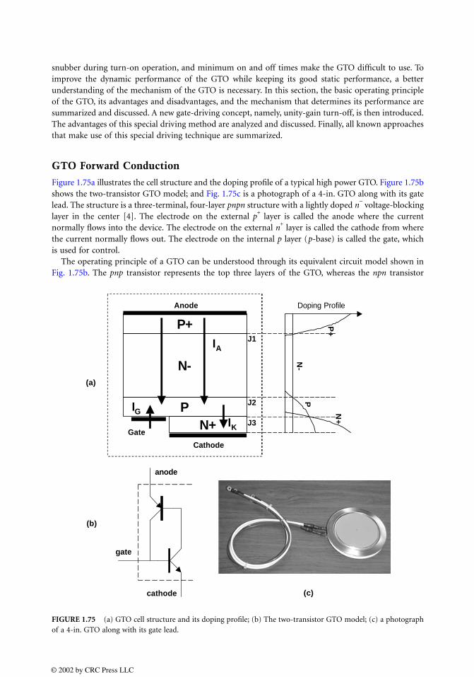
snubber during turn-on operation, and minimum on and off times make the GTO difficult to use. Toimprove the dynamic performance of the GTO while keeping its good static performance, a betterunderstanding of the mechanism of the GTO is necessary. In this section, the basic operating principleof the GTO, its advantages and disadvantages, and the mechanism that determines its performance aresummarized and discussed. A new gate-driving concept, namely, unity-gain turn-off, is then introduced.The advantages of this special driving method are analyzed and discussed. Finally, all known approachesthat make use of this special driving technique are summarized.
GTO Forward Conduction
Figure 1.75a illustrates the cell structure and the doping profile of a typical high power GTO. Figure 1.75bshows the two-transistor GTO model; and Fig. 1.75c is a photograph of a 4-in. GTO along with its gatelead. The structure is a three-terminal, four-layer pnpn structure with a lightly doped n
− voltage-blocking
layer in the center [4]. The electrode on the external p+ layer is called the anode where the current
normally flows into the device. The electrode on the external n+ layer is called the cathode from where
the current normally flows out. The electrode on the internal p layer (p-base) is called the gate, whichis used for control.
The operating principle of a GTO can be understood through its equivalent circuit model shown inFig. 1.75b. The pnp transistor represents the top three layers of the GTO, whereas the npn transistor
FIGURE 1.75 (a) GTO cell structure and its doping profile; (b) The two-transistor GTO model; (c) a photographof a 4-in. GTO along with its gate lead.
P+
N-
PN+
Anode
Gate
Cathode
IA
IGIK
J1
J2
J3
Doping Profile
P+
N-
P
N+
anode
gate
cathode
(a)
(b)
(c)
© 2002 by CRC Press LLC
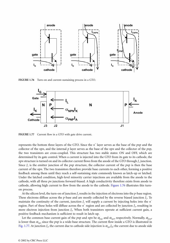
represents the bottom three layers of the GTO. Since the n− layer serves as the base of the pnp and the
collector of the npn, and the internal p layer serves as the base of the npn and the collector of the pnp,the two transistors are cross-coupled. This structure has two stable states: ON and OFF, which aredetermined by its gate control. When a current is injected into the GTO from its gate to its cathode, thenpn structure is turned on and its collector current flows from the anode of the GTO through J1 junction.Since J1 is the emitter junction of the pnp structure, the collector current of the pnp is then the basecurrent of the npn. The two transistors therefore provide base currents to each other, forming a positivefeedback among them until they reach a self-sustaining state commonly known as latch-up or latched.Under the latched condition, high-level minority carrier injections are available from the anode to thecathode, with all three pn junctions forward-biased. A high conductivity therefore exists from anode tocathode, allowing high current to flow from the anode to the cathode. Figure 1.76 illustrates this turn-on process.
At the silicon level, the turn-on of junction J3 results in the injection of electrons into the p-base region.These electrons diffuse across the p-base and are mostly collected by the reverse biased junction J2. Tomaintain the continuity of the current, junction J1 will supply a current by injecting holes into the n
−
region. Part of these holes will diffuse across the n− region and are collected by junction J2, resulting in
more electron injection from junction J3. When both transistors operate at sufficient current gain, apositive feedback mechanism is sufficient to result in latch-up.
Let the common base current gain of the pnp and npn be αpnp and αnpn, respectively. Normally, αpnpP
is lower than αnpn since the pnp is a wide-base structure. The current flow inside a GTO is illustrated inFig. 1.77. At junction J2, the current due to cathode side injection is αnpnIK; the current due to anode side
FIGURE 1.76 Turn-on and current-sustaining process in a GTO.
FIGURE 1.77 Current flow in a GTO with gate drive current.
© 2002 by CRC Press LLC
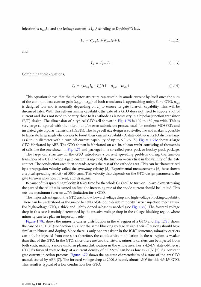
injection is αpnpIA; and the leakage current is IL. According to Kirchhoff ’s law,
(1.12)
and
(1.13)
Combining these equations,
(1.14)
This equation shows that the thyristor structure can sustain its anode current by itself once the sumof the common base current gain (αpnp + αnpn) of both transistors is approaching unity. For a GTO, αnpn
is designed low and is normally depending on IG to ensure its gate turn-off capability. This will bediscussed later. With this self-sustaining capability, the gate of a GTO does not need to supply a lot ofcurrent and does not need to be very close to its cathode as is necessary in a bipolar junction transistor(BJT) design. The dimension of a typical GTO cell shown in Fig. 1.75 is 100 to 150 µm wide. This isvery large compared with the micron and/or even submicron process used for modern MOSFETs andinsulated gate bipolar transistors (IGBTs). The large cell size design is cost-effective and makes it possibleto fabricate large single-die devices to boost their current capability. A state-of-the-art GTO die is as largeas 6-in. in diameter with a turn-off current capability of up to 6.0 kA [3]. Figure 1.75c shows a largeGTO fabricated by ABB. The GTO shown is fabricated on a 4-in. silicon wafer consisting of thousandsof cells like the one shown in Fig. 1.75 and packaged in a so-called press-pack or hockey-puck package.
The large cell structure in the GTO introduces a current spreading problem during the turn-ontransition of a GTO. When a gate current is injected, the turn-on occurs first in the vicinity of the gatecontact. The conduction area then spreads across the rest of the cathode area. This can be characterizedby a propagation velocity called the spreading velocity [5]. Experimental measurements [6] have showna typical spreading velocity of 5000 cm/s. This velocity also depends on the GTO design parameters, thegate turn-on injection current, and its dIG/dt.
Because of this spreading velocity, it takes time for the whole GTO cell to turn on. To avoid overstressingthe part of the cell that is turned on first, the increasing rate of the anode current should be limited. Thissets the maximum turn-on dI/dt limitation for a GTO.
The major advantages of the GTO are its low forward voltage drop and high-voltage blocking capability.These can be understood as the major benefits of its double-side minority carrier injection mechanism.For high-voltage GTO, a thick and lightly doped n-base is needed (see Fig. 1.75). The forward voltagedrop in this case is mainly determined by the resistive voltage drop in the voltage-blocking region whereminority carriers play an important role.
Figure 1.78a shows the minority carrier distribution in the n− region of a GTO and Fig. 1.78b shows
the case of an IGBT (see Section 1.9). For the same blocking voltage design, their n− regions should have
similar thickness and doping. Since there is only one transistor in the IGBT structure, minority carrierscan only be injected from one side; therefore, the conductivity modulation in the n
− region is weaker
than that of the GTO. In the GTO, since there are two transistors, minority carriers can be injected fromboth ends, making a more uniform plasma distribution in the whole area. For a 4.5-kV state-of-the-artGTO, its forward voltage drop at a current density of 50 A/cm
2 can be as low as 2.0 V [7] if a constant
gate current injection presents. Figure 1.79 shows the on-state characteristics of a state-of-the-art GTOmanufactured by ABB [7]. The forward voltage drop at 2000 A is only about 1.5 V for this 4.5-kV GTO.This result is typical of a low conduction loss GTO.
IA αpnpIA αnpnIK IL+ +=
IA IK IG–=
IA (αpnpIG IL)/+ (1 αpnp αnpn)––=
© 2002 by CRC Press LLC
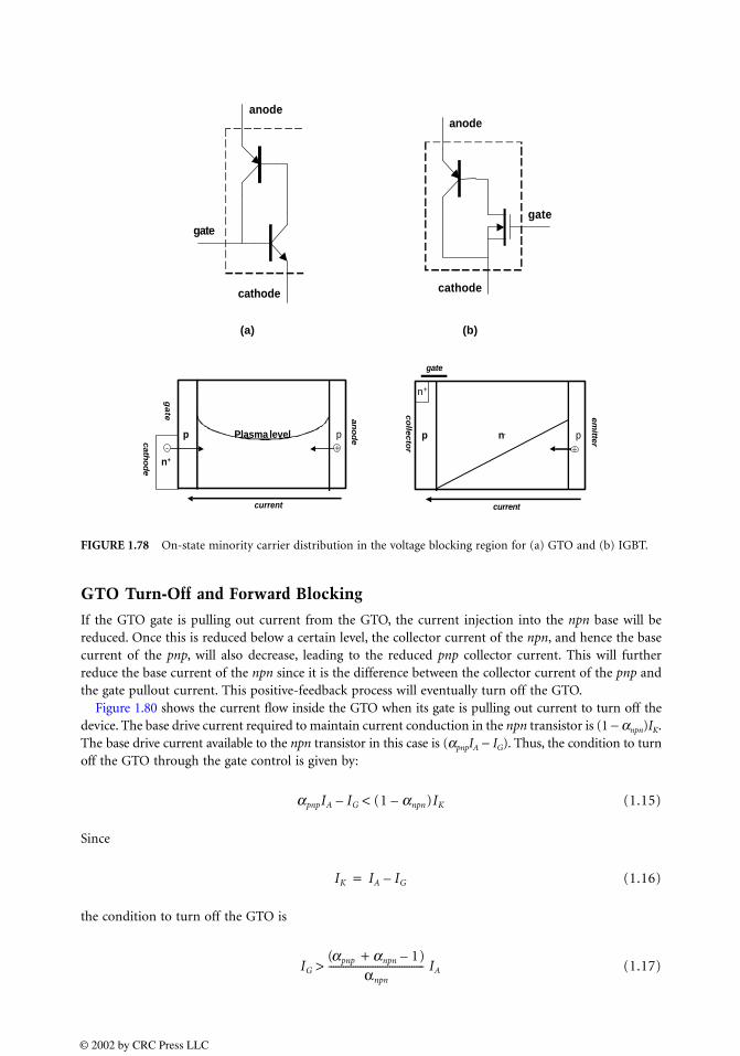
GTO Turn-Off and Forward Blocking
If the GTO gate is pulling out current from the GTO, the current injection into the npn base will bereduced. Once this is reduced below a certain level, the collector current of the npn, and hence the basecurrent of the pnp, will also decrease, leading to the reduced pnp collector current. This will furtherreduce the base current of the npn since it is the difference between the collector current of the pnp andthe gate pullout current. This positive-feedback process will eventually turn off the GTO.
Figure 1.80 shows the current flow inside the GTO when its gate is pulling out current to turn off thedevice. The base drive current required to maintain current conduction in the npn transistor is (1 − αnpn)IK.The base drive current available to the npn transistor in this case is (αpnpIA − IG). Thus, the condition to turnoff the GTO through the gate control is given by:
(1.15)
Since
(1.16)
the condition to turn off the GTO is
(1.17)
FIGURE 1.78 On-state minority carrier distribution in the voltage blocking region for (a) GTO and (b) IGBT.
anode
gate
cathode
anode
gate
cathode
p Plasma level p
n+
+
current
ano
decath
od
e
ga
te
p n- p+
current
gate
co
llec
tor
emitter
n+
(a) (b)
αpnpIA IG– (1 αnpn)IK–<
IK IA IG–=
IG
(αpnp αnpn 1)–+αnpn
--------------------------------------- IA>
© 2002 by CRC Press LLC
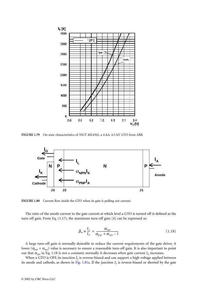
The ratio of the anode current to the gate current at which level a GTO is turned off is defined as theturn-off gain. From Eq. (1.17), the maximum turn-off gain [4] can be expressed as:
(1.18)
A large turn-off gain is normally desirable to reduce the current requirements of the gate driver. Alower (αpnp + αnpn) value is necessary to ensure a reasonable turn-off gain. It is also important to pointout that αnpn in Eq. 1.18 is not a constant; normally it decreases when gate current IG increases.
When a GTO is OFF, its junction J2 is reverse-biased and can support a high voltage applied betweenits anode and cathode, as shown in Fig. 1.81a. If the junction J3 is reverse-biased or shorted by the gate
FIGURE 1.79 On-state characteristics of 5SGT 40L4502, a 4-kA, 4.5-kV GTO from ABB.
FIGURE 1.80 Current flow inside the GTO when its gate is pulling out current.
PN
Anode
Cathode
Gate
J3 J2 J1
IA
IK
IG
αPNPIA
αNPNIK
ILN P
βm
IA
IG
----≡αnpn
αpnp αnpn 1–+----------------------------------=
© 2002 by CRC Press LLC
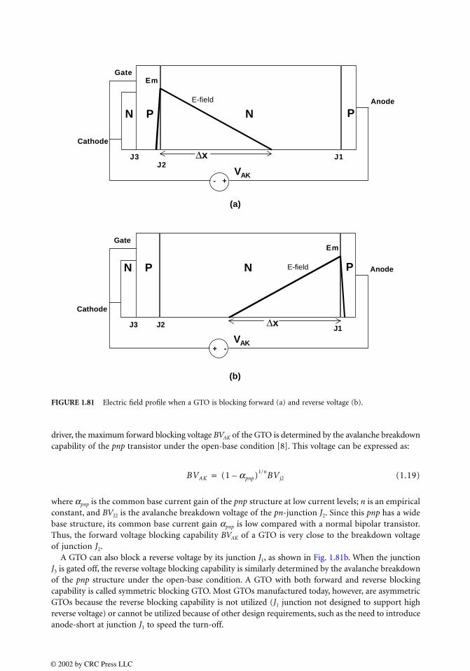
driver, the maximum forward blocking voltage BVAK of the GTO is determined by the avalanche breakdowncapability of the pnp transistor under the open-base condition [8]. This voltage can be expressed as:
(1.19)
where αpnp is the common base current gain of the pnp structure at low current levels; n is an empiricalconstant, and BVJ2 is the avalanche breakdown voltage of the pn-junction J2. Since this pnp has a widebase structure, its common base current gain αpnp is low compared with a normal bipolar transistor.Thus, the forward voltage blocking capability BVAK of a GTO is very close to the breakdown voltageof junction J2.
A GTO can also block a reverse voltage by its junction J1, as shown in Fig. 1.81b. When the junctionJ3 is gated off, the reverse voltage blocking capability is similarly determined by the avalanche breakdownof the pnp structure under the open-base condition. A GTO with both forward and reverse blockingcapability is called symmetric blocking GTO. Most GTOs manufactured today, however, are asymmetricGTOs because the reverse blocking capability is not utilized (J1 junction not designed to support highreverse voltage) or cannot be utilized because of other design requirements, such as the need to introduceanode-short at junction J1 to speed the turn-off.
FIGURE 1.81 Electric field profile when a GTO is blocking forward (a) and reverse voltage (b).
Em
Anode
∆xCathode
Gate
- +VAK
J3J2
J1
E-field
Em
Anode
∆xCathode
Gate
+ -VAK
J3 J2 J1
E-field
(a)
(b)
PN N P
PN N P
BVAK (1 αpnp)1/n– BVj2=
© 2002 by CRC Press LLC
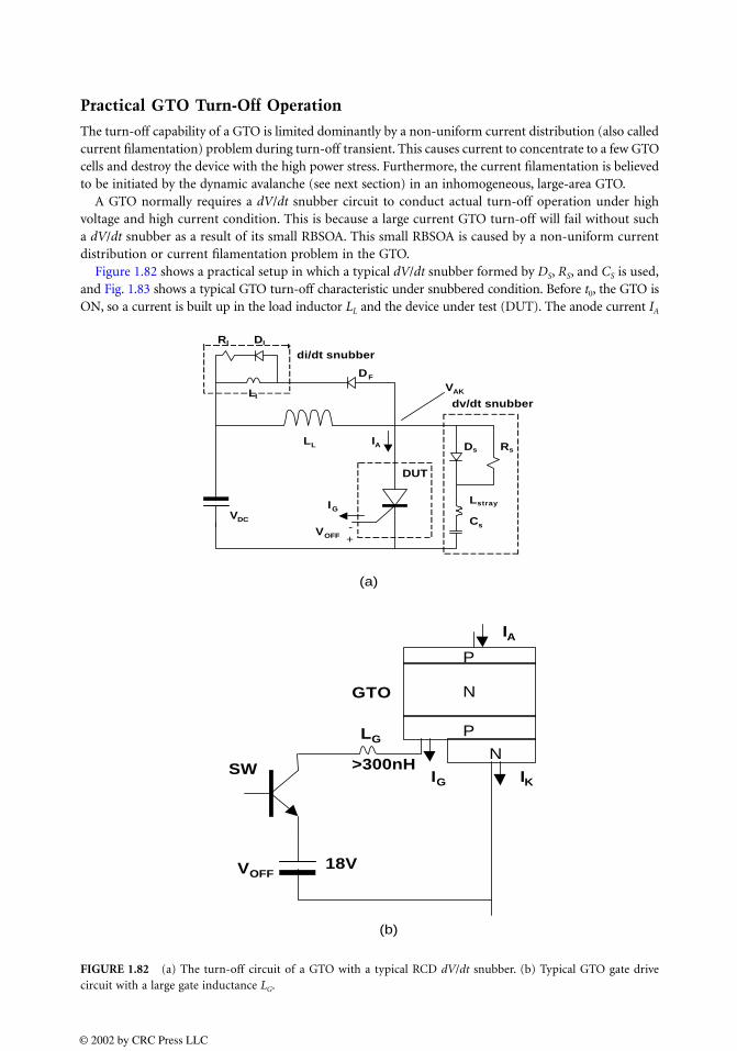
Practical GTO Turn-Off Operation
The turn-off capability of a GTO is limited dominantly by a non-uniform current distribution (also calledcurrent filamentation) problem during turn-off transient. This causes current to concentrate to a few GTOcells and destroy the device with the high power stress. Furthermore, the current filamentation is believedto be initiated by the dynamic avalanche (see next section) in an inhomogeneous, large-area GTO.
A GTO normally requires a dV/dt snubber circuit to conduct actual turn-off operation under highvoltage and high current condition. This is because a large current GTO turn-off will fail without sucha dV/dt snubber as a result of its small RBSOA. This small RBSOA is caused by a non-uniform currentdistribution or current filamentation problem in the GTO.
Figure 1.82 shows a practical setup in which a typical dV/dt snubber formed by DS, RS, and CS is used,and Fig. 1.83 shows a typical GTO turn-off characteristic under snubbered condition. Before t0, the GTO isON, so a current is built up in the load inductor LL and the device under test (DUT). The anode current IA
FIGURE 1.82 (a) The turn-off circuit of a GTO with a typical RCD dV/dt snubber. (b) Typical GTO gate drivecircuit with a large gate inductance LG.
DUT
VDC Cs
Ds RsLL IA
VAK
IG
DF
di/dt snubber
Lstray
LI
DIRI
dv/dt snubber
-+
VOFF
LG
>300nH
18V
GTO
P
N
P
N
IA
IKIG
VOFF
SW
(a)
(b)
© 2002 by CRC Press LLC
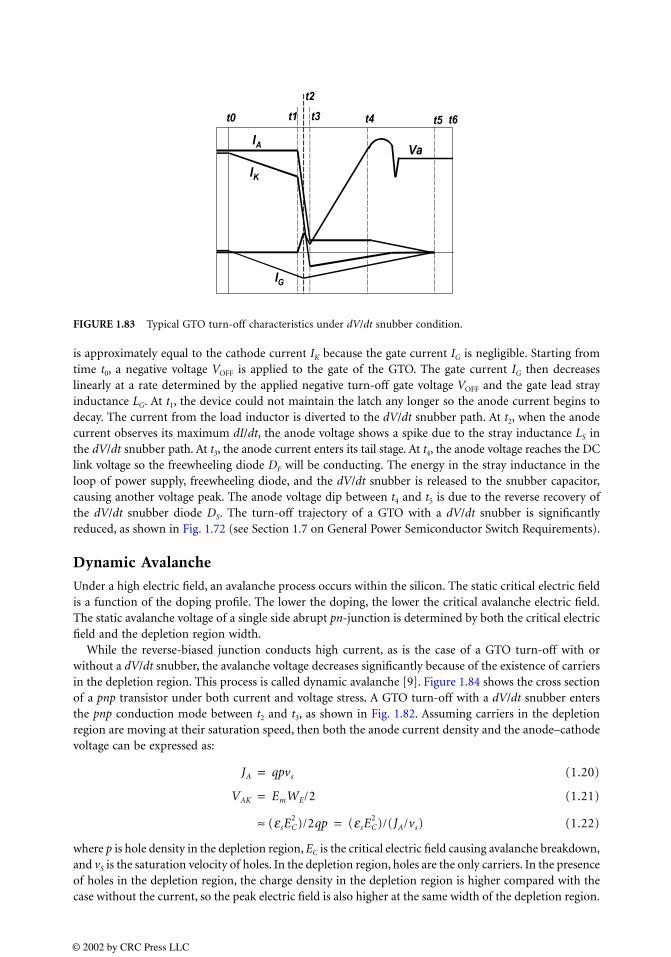
is approximately equal to the cathode current IK because the gate current IG is negligible. Starting fromtime t0, a negative voltage VOFF is applied to the gate of the GTO. The gate current IG then decreaseslinearly at a rate determined by the applied negative turn-off gate voltage VOFF and the gate lead strayinductance LG. At t1, the device could not maintain the latch any longer so the anode current begins todecay. The current from the load inductor is diverted to the dV/dt snubber path. At t2, when the anodecurrent observes its maximum dI/dt, the anode voltage shows a spike due to the stray inductance LS inthe dV/dt snubber path. At t3, the anode current enters its tail stage. At t4, the anode voltage reaches the DClink voltage so the freewheeling diode DF will be conducting. The energy in the stray inductance in theloop of power supply, freewheeling diode, and the dV/dt snubber is released to the snubber capacitor,causing another voltage peak. The anode voltage dip between t4 and t5 is due to the reverse recovery ofthe dV/dt snubber diode DS. The turn-off trajectory of a GTO with a dV/dt snubber is significantlyreduced, as shown in Fig. 1.72 (see Section 1.7 on General Power Semiconductor Switch Requirements).
Dynamic Avalanche
Under a high electric field, an avalanche process occurs within the silicon. The static critical electric fieldis a function of the doping profile. The lower the doping, the lower the critical avalanche electric field.The static avalanche voltage of a single side abrupt pn-junction is determined by both the critical electricfield and the depletion region width.
While the reverse-biased junction conducts high current, as is the case of a GTO turn-off with orwithout a dV/dt snubber, the avalanche voltage decreases significantly because of the existence of carriersin the depletion region. This process is called dynamic avalanche [9]. Figure 1.84 shows the cross sectionof a pnp transistor under both current and voltage stress. A GTO turn-off with a dV/dt snubber entersthe pnp conduction mode between t2 and t3, as shown in Fig. 1.82. Assuming carriers in the depletionregion are moving at their saturation speed, then both the anode current density and the anode–cathodevoltage can be expressed as:
(1.20)
(1.21)
(1.22)
where p is hole density in the depletion region, EC is the critical electric field causing avalanche breakdown,and vS is the saturation velocity of holes. In the depletion region, holes are the only carriers. In the presenceof holes in the depletion region, the charge density in the depletion region is higher compared with thecase without the current, so the peak electric field is also higher at the same width of the depletion region.
FIGURE 1.83 Typical GTO turn-off characteristics under dV/dt snubber condition.
JA qpvs=
VAK EmWE/2=
(εsEC2 )/2qp≈ (εsEC
2 )/(JA/vs)=
© 2002 by CRC Press LLC
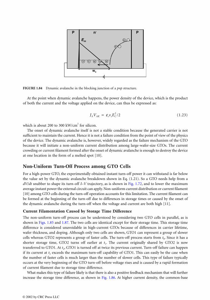
At the point when dynamic avalanche happens, the power density of the device, which is the productof both the current and the voltage applied on the device, can thus be expressed as:
(1.23)
which is about 200 to 300 kW/cm2 for silicon.
The onset of dynamic avalanche itself is not a stable condition because the generated carrier is notsufficient to maintain the current. Hence it is not a failure condition from the point of view of the physicsof the device. The dynamic avalanche is, however, widely regarded as the failure mechanism of the GTObecause it will initiate a non-uniform current distribution among large-wafer-size GTOs. The currentcrowding or current filament formed after the onset of dynamic avalanche is enough to destroy the deviceat one location in the form of a melted spot [10].
Non-Uniform Turn-Off Process among GTO Cells
For a high-power GTO, the experimentally obtained instant turn-off power it can withstand is far belowthe value set by the dynamic avalanche breakdown shown in Eq. (1.21). So a GTO needs help from adV/dt snubber to shape its turn-off I–V trajectory, as is shown in Fig. 1.72, and to lower the maximumaverage instant power the external circuit can apply. Non-uniform current distribution or current filament[10] among GTO cells during the turn-off operation accounts for this limitation. The current filament canbe formed at the beginning of the turn-off due to differences in storage times or caused by the onset ofthe dynamic avalanche during the turn-off when the voltage and current are both high [11].
Current Filamentation Caused by Storage Time Difference
The non-uniform turn-off process can be understood by considering two GTO cells in parallel, as isshown in Figs. 1.85 and 1.87. The two cells are identical except for their storage time. This storage timedifference is considered unavoidable in high-current GTOs because of differences in carrier lifetime,wafer thickness, and doping. Although only two cells are shown, GTO1 can represent a group of slowercells whereas GTO2 represents a group of faster cells. The turn-off process starts from t0. Since it has ashorter storage time, GTO2 turns off earlier at t1. The current originally shared by GTO2 is nowtransferred to GTO1. At t2, GTO1 is turned off at twice its previous current. Turn-off failure can happenif its current at t2 exceeds the maximum turn-off capability of GTO1. This can easily be the case whenthe number of faster cells is much larger than the number of slower cells. This type of failure typicallyoccurs at the very beginning of the GTO turn-off before voltage rises and is caused by a rapid formationof current filament due to storage time difference.
What makes this type of failure likely is that there is also a positive feedback mechanism that will furtherincrease the storage time difference, as shown in Fig. 1.86. At higher current density, the common-base
FIGURE 1.84 Dynamic avalanche in the blocking junction of a pnp structure.
JAVAK εsvsEC2 /2=
© 2002 by CRC Press LLC
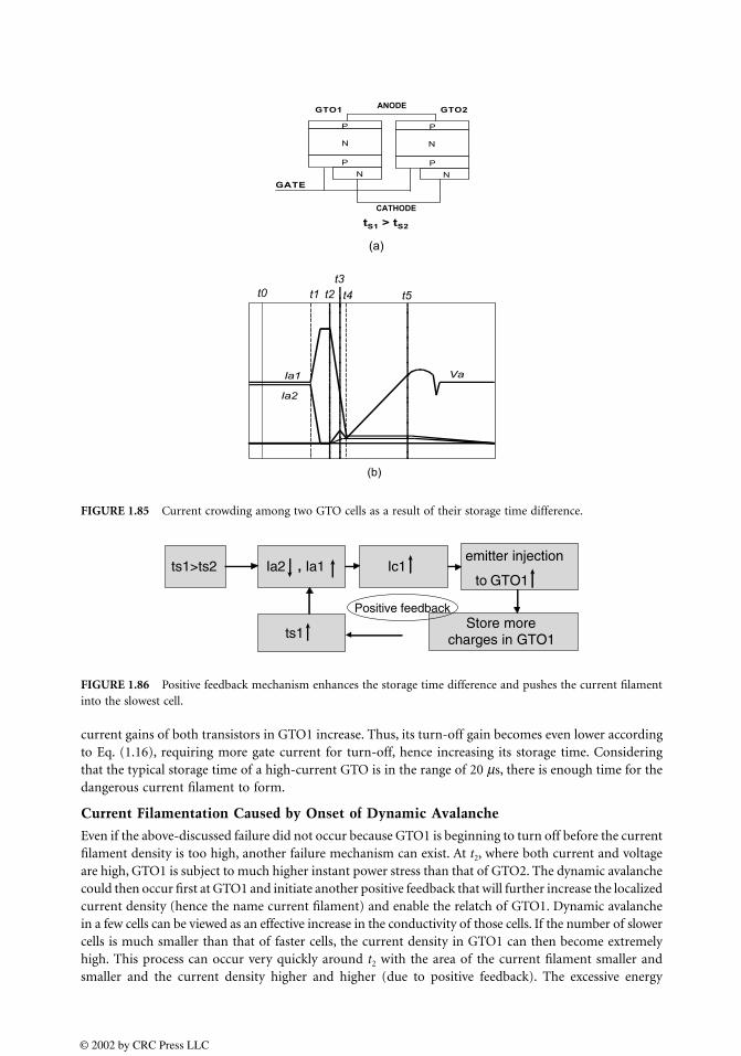
current gains of both transistors in GTO1 increase. Thus, its turn-off gain becomes even lower accordingto Eq. (1.16), requiring more gate current for turn-off, hence increasing its storage time. Consideringthat the typical storage time of a high-current GTO is in the range of 20 µs, there is enough time for thedangerous current filament to form.
Current Filamentation Caused by Onset of Dynamic Avalanche
Even if the above-discussed failure did not occur because GTO1 is beginning to turn off before the currentfilament density is too high, another failure mechanism can exist. At t2, where both current and voltageare high, GTO1 is subject to much higher instant power stress than that of GTO2. The dynamic avalanchecould then occur first at GTO1 and initiate another positive feedback that will further increase the localizedcurrent density (hence the name current filament) and enable the relatch of GTO1. Dynamic avalanchein a few cells can be viewed as an effective increase in the conductivity of those cells. If the number of slowercells is much smaller than that of faster cells, the current density in GTO1 can then become extremelyhigh. This process can occur very quickly around t2 with the area of the current filament smaller andsmaller and the current density higher and higher (due to positive feedback). The excessive energy
FIGURE 1.85 Current crowding among two GTO cells as a result of their storage time difference.
FIGURE 1.86 Positive feedback mechanism enhances the storage time difference and pushes the current filamentinto the slowest cell.
ts1>ts2 Ia2 Ia1 Ic1 emitter injection
to GTO1
Store morecharges in GTO1ts1
Positive feedback
© 2002 by CRC Press LLC

dissipated on the stressed cells can cause permanent failure because the temperature can be very high.After the device failure, a GTO device loses its blocking capability and behaves resistively.
It can therefore be concluded that the combination of storage time differences and the onset ofpossible localized dynamic avalanche makes the turn-off capability of a GTO small. Practical RBSOAsof high-power GTOs are below the 50 kW/cm
2 power constant line. This low limitation mandates the
use of a dV/dt snubber. Even with a dV/dt snubber, GTO failure can still occur if the instant power istoo high at t2 and exceeds the RBSOA limit of the GTO at that time instance. The voltage spike at t2
can be reduced by minimizing the stray inductance of the dV/dt snubber. The size of the snubber (Cs
value) is typically between 3 to 6 µF. The disadvantages of using a dV/dt snubber are the increased countand size of the components, its high-energy loss, and its increased thermal management requirementto cool resistor Rs.
The concerns of non-uniform current distribution also mandate a minimum on-time rating for GTOsto ensure that conduction current is uniformly distributed in the ON state before a turn-off can beperformed. Minimum off-time is also a commonly used rating for the GTO to guarantee the tail currentof the GTO is completely gone and the GTO cells are all in the OFF state.
Summary
Advantages of the GTO include:
1. High current–voltage capability2. Low conduction loss3. Low cost
Disadvantages
1. Non-uniform turn-off—poor RBSOA and dV/dt snubber required2. Non-uniform turn-on—dI/dt snubber required3. Current control—high gating power4. Long switching time—long storage time, minimum on-time and off-time requirements5. No current limitation capability (FBSOA)
FIGURE 1.87 Semiconductor level analysis of the non-uniform turn-off process. The shaded region representsstored charge (plasma) in the GTO.
P
N
P
N
P
N
P
N
Ia
IcIg
t0Ia
P
N
P
N
P
N
P
N
IcIg
t1Ia
P
N
P
N
P
N
P
N
IcIg
t2
Ia
P
N
P
N
P
N
P
N
IcIg
t4Ia
P
N
P
N
P
N
P
N
IcIg
t3Ia
P
N
P
N
P
N
P
N
IcIg
t5
Ia1 Ia2
Ia1=Ia2 Ia1 Ia2 Ia1< Ia2
Ia1<<Ia2Ia1 Ia2Ia1 Ia2
≈
≈≈
© 2002 by CRC Press LLC
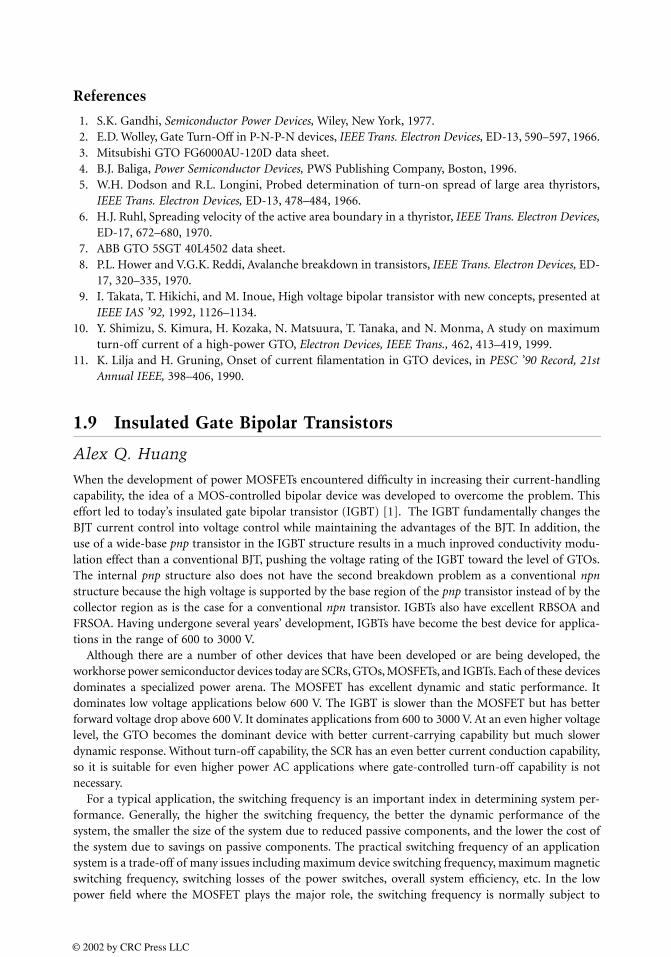
References
1. S.K. Gandhi, Semiconductor Power Devices, Wiley, New York, 1977.2. E.D. Wolley, Gate Turn-Off in P-N-P-N devices, IEEE Trans. Electron Devices, ED-13, 590–597, 1966.3. Mitsubishi GTO FG6000AU-120D data sheet.4. B.J. Baliga, Power Semiconductor Devices, PWS Publishing Company, Boston, 1996.5. W.H. Dodson and R.L. Longini, Probed determination of turn-on spread of large area thyristors,
IEEE Trans. Electron Devices, ED-13, 478–484, 1966.6. H.J. Ruhl, Spreading velocity of the active area boundary in a thyristor, IEEE Trans. Electron Devices,
ED-17, 672–680, 1970.7. ABB GTO 5SGT 40L4502 data sheet.8. P.L. Hower and V.G.K. Reddi, Avalanche breakdown in transistors, IEEE Trans. Electron Devices, ED-
17, 320–335, 1970.9. I. Takata, T. Hikichi, and M. Inoue, High voltage bipolar transistor with new concepts, presented at
IEEE IAS ’92, 1992, 1126–1134.10. Y. Shimizu, S. Kimura, H. Kozaka, N. Matsuura, T. Tanaka, and N. Monma, A study on maximum
turn-off current of a high-power GTO, Electron Devices, IEEE Trans., 462, 413–419, 1999.11. K. Lilja and H. Gruning, Onset of current filamentation in GTO devices, in PESC ’90 Record, 21st
Annual IEEE, 398–406, 1990.
1.9 Insulated Gate Bipolar Transistors
Alex Q. Huang
When the development of power MOSFETs encountered difficulty in increasing their current-handlingcapability, the idea of a MOS-controlled bipolar device was developed to overcome the problem. Thiseffort led to today’s insulated gate bipolar transistor (IGBT) [1]. The IGBT fundamentally changes theBJT current control into voltage control while maintaining the advantages of the BJT. In addition, theuse of a wide-base pnp transistor in the IGBT structure results in a much inproved conductivity modu-lation effect than a conventional BJT, pushing the voltage rating of the IGBT toward the level of GTOs.The internal pnp structure also does not have the second breakdown problem as a conventional npnstructure because the high voltage is supported by the base region of the pnp transistor instead of by thecollector region as is the case for a conventional npn transistor. IGBTs also have excellent RBSOA andFRSOA. Having undergone several years’ development, IGBTs have become the best device for applica-tions in the range of 600 to 3000 V.
Although there are a number of other devices that have been developed or are being developed, theworkhorse power semiconductor devices today are SCRs, GTOs, MOSFETs, and IGBTs. Each of these devicesdominates a specialized power arena. The MOSFET has excellent dynamic and static performance. Itdominates low voltage applications below 600 V. The IGBT is slower than the MOSFET but has betterforward voltage drop above 600 V. It dominates applications from 600 to 3000 V. At an even higher voltagelevel, the GTO becomes the dominant device with better current-carrying capability but much slowerdynamic response. Without turn-off capability, the SCR has an even better current conduction capability,so it is suitable for even higher power AC applications where gate-controlled turn-off capability is notnecessary.
For a typical application, the switching frequency is an important index in determining system per-formance. Generally, the higher the switching frequency, the better the dynamic performance of thesystem, the smaller the size of the system due to reduced passive components, and the lower the cost ofthe system due to savings on passive components. The practical switching frequency of an applicationsystem is a trade-off of many issues including maximum device switching frequency, maximum magneticswitching frequency, switching losses of the power switches, overall system efficiency, etc. In the lowpower field where the MOSFET plays the major role, the switching frequency is normally subject to
© 2002 by CRC Press LLC

system efficiency and/or magnetic considerations instead of device limitations. In the medium powerfield, where the IGBT plays the major role, the situation changes. At the lower end, the limitation of thedevice does not dominate since the lower-rating IGBT is normally fast enough. However, when the powerrating is higher, the IGBT switching speed decreases and the switching losses increase significantly. Thepractical switching frequency is thus subject to the limitation of the device. When the power level moveseven higher, the GTO is the only available device. Since it has several tens of microseconds switchingtime, significant turn-off, and dV/dt snubber loss, the GTO is traditionally the limitation of the switchingfrequency of the system.
The above trend shows that when the power level moves higher, power semiconductor devices limitthe maximum system switching frequency, hence the performance of the system, especially at the GTOlevel. To meet the increasing demand for better performance in high-power systems, many efforts havebeen made to improve the performance of high-power semiconductor devices. Among them, one effortis to push the IGBT toward higher power ratings based on the module concept. With its good dynamicperformance, high-power systems equipped with IGBTs can operate at a much higher switching frequencyand have many benefits compared with a conventional GTO system. The state-of-the-art IGBT rating iscurrently 3.3 kV/1.2 kA [2], which is at the low end of that of the GTO.
IGBT Structure and Operation
The name insulated gate bipolar transistor sterns from its operation based on an internal interactionbetween an insulated-gate FET (IGFET) and a bipolar transistor. It has previously been called an IGT(insulated-gate transistor), an IGR (insulated-gate rectifier), a COMFET (conductivity-modulated field-effect transistor), a GEMFET (gain-enhanced MOSFET), a BiFET (bipolar FET), and an injector FET.IGBTs have been successfully used since they were first demonstrated in 1982 and are currently the mostwidely used power semiconductor switches with applications from several kilowatts to a few megawatts.
A cross section of the planar junction–based IGBT structure introduced in the 1980s is shown inFig. 1.88a. The IGBT structure is similar to that of a planar power MOSFET except the difference in thesubstrate doping type. The fabrication of the IGBT therefore is almost the same as a power MOSFET.This has made its manufacture relatively easy immediately after conception, and its ratings have grownat a rapid pace as a result of the ability to scale up both the current and the blocking voltage ratings.Today, the largest single-chip IGBT can carry about 100 A and block more than 3000 V. Larger currentIGBTs are also introduced by paralleling more IGBT chips in a single package. These IGBTs are alsocalled IGBT modules. Figure 1.89 shows a photograph of a 1200-A, 3300-V IGBT module fabricated byMitsubishi.
FIGURE 1.88 (a) Cross section of the IGBT structure and (b) equivalent circuit for the IGBT.
collectorcollector
gate
PR
N drift
gate
n+
P+
emitter emitter
P substrate+J
1
J2
parasitic thyristor
PNP
NPN
a b
© 2002 by CRC Press LLC
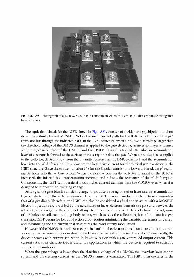
The equivalent circuit for the IGBT, shown in Fig. 1.88b, consists of a wide-base pnp bipolar transistordriven by a short-channel MOSFET. Notice the main current path for the IGBT is not through the pnptransistor but through the indicated path. In the IGBT structure, when a positive bias voltage larger thanthe threshold voltage of the DMOS channel is applied to the gate electrode, an inversion layer is formedalong the p-base surface of the DMOS, and the DMOS channel is turned ON. Also an accumulationlayer of electrons is formed at the surface of the n region below the gate. When a positive bias is appliedto the collector, electrons flow from the n
+ emitter contact via the DMOS channel and the accumulation
layer into the n− drift region. This provides the base drive current for the vertical pnp transistor in the
IGBT structure. Since the emitter junction (J1) for this bipolar transistor is forward-biased, the p+ region
injects holes into the n− base region. When the positive bias on the collector terminal of the IGBT is
increased, the injected hole concentration increases and reduces the resistance of the n− drift region.
Consequently, the IGBT can operate at much higher current densities than the VDMOS even when it isdesigned to support high blocking voltages.
As long as the gate bias is sufficiently large to produce a strong inversion layer and an accumulationlayer of electrons at the n
− base region surface, the IGBT forward conduction characteristic resembles
that of a pin diode. Therefore, the IGBT can also be considered a pin diode in series with a MOSFET.Electron injections are provided by the accumulation layer electrons beneath the gate and between theadjacent p-body regions. However, not all injected holes recombine with these electrons; instead, someof the holes are collected by the p-body region, which acts as the collector region of the parasitic pnptransistor. IGBT design for low conduction drop requires minimizing the parasitic pnp transistor currentand maximizing the pin current that maximizes the conductivity modulation.
However, if the DMOS channel becomes pinched off and the electron current saturates, the hole currentalso saturates because of the saturation of the base drive current for the pnp transistor. Consequently, thedevice operates with current saturation in its active region with a gate-controlled output current. Thiscurrent saturation characteristic is useful for applications in which the device is required to sustain ashort-circuit condition.
When the gate voltage is lower than the threshold voltage of the DMOS, the inversion layer cannotsustain and the electron current via the DMOS channel is terminated. The IGBT then operates in the
FIGURE 1.89 Photograph of a 1200-A, 3300-V IGBT module in which 24 1-cm2 IGBT dies are paralleled together
by wire bonds.
© 2002 by CRC Press LLC

forward blocking mode. A large voltage can then be supported by the reverse-biased p-base/n-driftjunction (J2). Figure 1.90 shows a typical output characteristic of the IGBT.
The IGBT was the first commercially successful device based upon combining the physics of MOS-gatecontrol with bipolar current conduction. Due to the injection of a high concentration of holes from thep
+ substrate into the n
− drift, the conductivity of the long n
− region is modulated and the IGBT exhibits
pin diodelike on-state characteristics with a low forward voltage drop. Thus, the IGBT exhibits excellentcurrent-carrying characteristics with forward conduction current densities 20 times higher than that ofa power MOSFET and five times greater than that of a bipolar transistor operating at a current gain of 10.Since the input signal for the IGBT is a voltage applied to the MOS-gate, the IGBT has the high inputimpedance of the power MOSFET and can be classified as a voltage-controlled device. However, unlikethe power MOSFET, the switching speed of the IGBT is limited by the time taken to remove the storedcharges in the drift region due to the injection of holes during on-state current conduction. The turn-off time for the IGBT is dictated by the conduction modulation of the drift region and the minoritycarrier lifetime. The frontier is specified dominantly by the current gain of the wide-base pnp transistor,and the latter can be controlled by a lifetime control process, such as electron irradiation. Although thelifetime control process can be successful in reducing the turn-off time, it was found that there was atrade-off between the on-state voltage drop (conduction loss) and the turn-off time (switching loss). Ashorter minority carrier lifetime makes the switching loss of the IGBT lower, but the shorter minoritycarrier lifetime also results in a higher conduction loss.
One of the problems encountered when operating the IGBT at high current levels has been the latch-upof the parasitic pnpn thyristor structure inherent in the device structure. Latch-up of this thyristor canoccur, causing losses of gate-controlled current conduction. Since the current gains of the npn and pnptransistors increase with increasing temperature, the latching current decreases with increasing temper-ature. This effect is also aggravated by an increase in the resistance of the p-base with temperature dueto a decrease in the mobility of holes. Many methods have been explored to suppress the latch-up of theparasitic thyristor, such as the use of a deep p
+ diffusion, a shallow p
+ diffusion, or a self-aligned sidewall
diffusion of n+ emitter. State-of-the-art IGBTs have basically solved this problem, and latch-up does not
occur for all gate voltages applied. These IGBTs therefore exhibit close to square FBSOA.Traditionally, IGBTs are fabricated on a lightly doped epitaxial substrate, such as the one shown in
Fig. 1.88a. Because of the difficulty of growing the lightly doped epitaxial layer, the breakdown voltageof this type of IGBT is limited to below 1000 V. To benefit from such a design, an n buffer layer is normallyintroduced between the p
+ substrate and the n
− epitaxial layer, so that the whole n
− drift region is depleted
when the device is blocking the off-state voltage, and the electric field shape within the n− drift region
is close to rectangular. This type of design is referred to as Punch-Through IGBT (PT IGBT), as shownin Fig. 1.91a. The PT structure allows it to support the same forward blocking voltage with about halfthe thickness of the n
− base region of the pnp transistor, resulting in a greatly improved trade-off rela-
tionship between the forward voltage drop and the turn-off time. Thus, the PT structure together withlifetime control is preferred for IGBTs with forward blocking capabilities of up to 1200 V.
FIGURE 1.90 Output characteristics of the IGBT.
forwardcharacteristics
reversecharacteristics
VCE
ICE
VG
© 2002 by CRC Press LLC
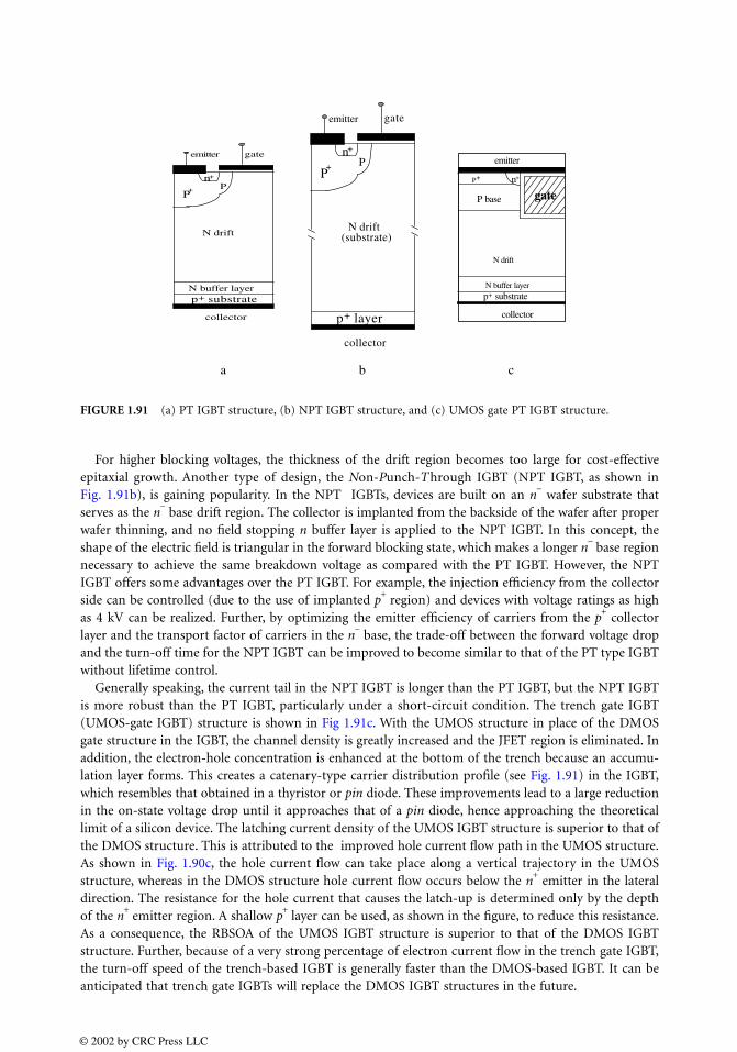
For higher blocking voltages, the thickness of the drift region becomes too large for cost-effectiveepitaxial growth. Another type of design, the Non-Punch-Through IGBT (NPT IGBT, as shown inFig. 1.91b), is gaining popularity. In the NPT IGBTs, devices are built on an n
− wafer substrate that
serves as the n− base drift region. The collector is implanted from the backside of the wafer after proper
wafer thinning, and no field stopping n buffer layer is applied to the NPT IGBT. In this concept, theshape of the electric field is triangular in the forward blocking state, which makes a longer n
− base region
necessary to achieve the same breakdown voltage as compared with the PT IGBT. However, the NPTIGBT offers some advantages over the PT IGBT. For example, the injection efficiency from the collectorside can be controlled (due to the use of implanted p
+ region) and devices with voltage ratings as high
as 4 kV can be realized. Further, by optimizing the emitter efficiency of carriers from the p+ collector
layer and the transport factor of carriers in the n− base, the trade-off between the forward voltage drop
and the turn-off time for the NPT IGBT can be improved to become similar to that of the PT type IGBTwithout lifetime control.
Generally speaking, the current tail in the NPT IGBT is longer than the PT IGBT, but the NPT IGBTis more robust than the PT IGBT, particularly under a short-circuit condition. The trench gate IGBT(UMOS-gate IGBT) structure is shown in Fig 1.91c. With the UMOS structure in place of the DMOSgate structure in the IGBT, the channel density is greatly increased and the JFET region is eliminated. Inaddition, the electron-hole concentration is enhanced at the bottom of the trench because an accumu-lation layer forms. This creates a catenary-type carrier distribution profile (see Fig. 1.91) in the IGBT,which resembles that obtained in a thyristor or pin diode. These improvements lead to a large reductionin the on-state voltage drop until it approaches that of a pin diode, hence approaching the theoreticallimit of a silicon device. The latching current density of the UMOS IGBT structure is superior to that ofthe DMOS structure. This is attributed to the improved hole current flow path in the UMOS structure.As shown in Fig. 1.90c, the hole current flow can take place along a vertical trajectory in the UMOSstructure, whereas in the DMOS structure hole current flow occurs below the n
+ emitter in the lateral
direction. The resistance for the hole current that causes the latch-up is determined only by the depthof the n
+ emitter region. A shallow p
+ layer can be used, as shown in the figure, to reduce this resistance.
As a consequence, the RBSOA of the UMOS IGBT structure is superior to that of the DMOS IGBTstructure. Further, because of a very strong percentage of electron current flow in the trench gate IGBT,the turn-off speed of the trench-based IGBT is generally faster than the DMOS-based IGBT. It can beanticipated that trench gate IGBTs will replace the DMOS IGBT structures in the future.
FIGURE 1.91 (a) PT IGBT structure, (b) NPT IGBT structure, and (c) UMOS gate PT IGBT structure.
collector
gate
P
N drift
n+
P+
emitter
N buffer layerp substrate+
collector
gate
P
N drift (substrate)
n+
P+
emitter
p layer+ collector
gateP base
N drift
n+
emitter
N buffer layerp substrate+
P+
a b c
© 2002 by CRC Press LLC
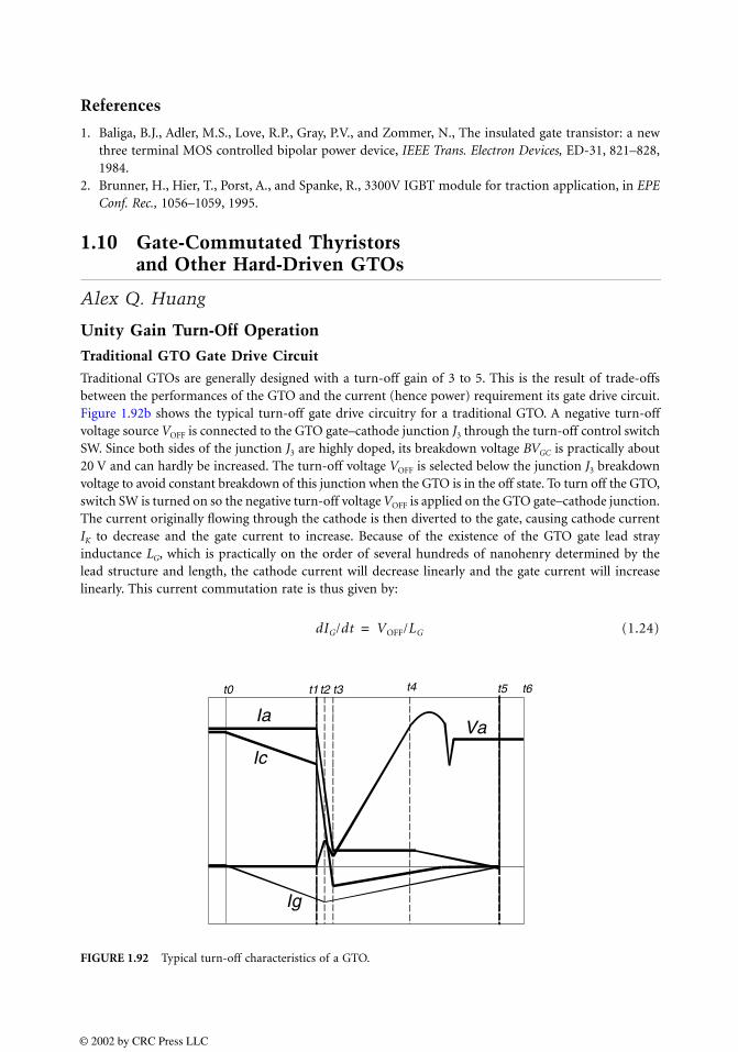
References
1. Baliga, B.J., Adler, M.S., Love, R.P., Gray, P.V., and Zommer, N., The insulated gate transistor: a newthree terminal MOS controlled bipolar power device, IEEE Trans. Electron Devices, ED-31, 821–828,1984.
2. Brunner, H., Hier, T., Porst, A., and Spanke, R., 3300V IGBT module for traction application, in EPEConf. Rec., 1056–1059, 1995.
1.10 Gate-Commutated Thyristors and Other Hard-Driven GTOs
Alex Q. Huang
Unity Gain Turn-Off Operation
Traditional GTO Gate Drive Circuit
Traditional GTOs are generally designed with a turn-off gain of 3 to 5. This is the result of trade-offsbetween the performances of the GTO and the current (hence power) requirement its gate drive circuit.Figure 1.92b shows the typical turn-off gate drive circuitry for a traditional GTO. A negative turn-offvoltage source VOFF is connected to the GTO gate–cathode junction J3 through the turn-off control switchSW. Since both sides of the junction J3 are highly doped, its breakdown voltage BVGC is practically about20 V and can hardly be increased. The turn-off voltage VOFF is selected below the junction J3 breakdownvoltage to avoid constant breakdown of this junction when the GTO is in the off state. To turn off the GTO,switch SW is turned on so the negative turn-off voltage VOFF is applied on the GTO gate–cathode junction.The current originally flowing through the cathode is then diverted to the gate, causing cathode currentIK to decrease and the gate current to increase. Because of the existence of the GTO gate lead strayinductance LG, which is practically on the order of several hundreds of nanohenry determined by thelead structure and length, the cathode current will decrease linearly and the gate current will increaselinearly. This current commutation rate is thus given by:
(1.24)
FIGURE 1.92 Typical turn-off characteristics of a GTO.
dIG/dt VOFF/LG=
Ia
Ic
Ig
Va
t0 t1 t2 t3 t4 t5 t6
© 2002 by CRC Press LLC
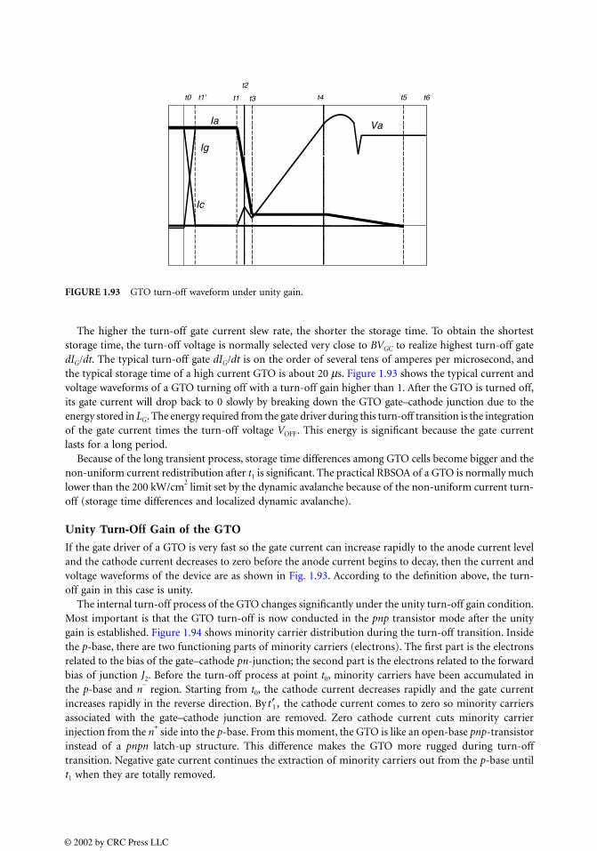
The higher the turn-off gate current slew rate, the shorter the storage time. To obtain the shorteststorage time, the turn-off voltage is normally selected very close to BVGC to realize highest turn-off gatedIG/dt. The typical turn-off gate dIG/dt is on the order of several tens of amperes per microsecond, andthe typical storage time of a high current GTO is about 20 µs. Figure 1.93 shows the typical current andvoltage waveforms of a GTO turning off with a turn-off gain higher than 1. After the GTO is turned off,its gate current will drop back to 0 slowly by breaking down the GTO gate–cathode junction due to theenergy stored in LG. The energy required from the gate driver during this turn-off transition is the integrationof the gate current times the turn-off voltage VOFF. This energy is significant because the gate currentlasts for a long period.
Because of the long transient process, storage time differences among GTO cells become bigger and thenon-uniform current redistribution after t1 is significant. The practical RBSOA of a GTO is normally muchlower than the 200 kW/cm
2 limit set by the dynamic avalanche because of the non-uniform current turn-
off (storage time differences and localized dynamic avalanche).
Unity Turn-Off Gain of the GTO
If the gate driver of a GTO is very fast so the gate current can increase rapidly to the anode current leveland the cathode current decreases to zero before the anode current begins to decay, then the current andvoltage waveforms of the device are as shown in Fig. 1.93. According to the definition above, the turn-off gain in this case is unity.
The internal turn-off process of the GTO changes significantly under the unity turn-off gain condition.Most important is that the GTO turn-off is now conducted in the pnp transistor mode after the unitygain is established. Figure 1.94 shows minority carrier distribution during the turn-off transition. Insidethe p-base, there are two functioning parts of minority carriers (electrons). The first part is the electronsrelated to the bias of the gate–cathode pn-junction; the second part is the electrons related to the forwardbias of junction J2. Before the turn-off process at point t0, minority carriers have been accumulated inthe p-base and n
− region. Starting from t0, the cathode current decreases rapidly and the gate current
increases rapidly in the reverse direction. By the cathode current comes to zero so minority carriersassociated with the gate–cathode junction are removed. Zero cathode current cuts minority carrierinjection from the n
+ side into the p-base. From this moment, the GTO is like an open-base pnp-transistor
instead of a pnpn latch-up structure. This difference makes the GTO more rugged during turn-offtransition. Negative gate current continues the extraction of minority carriers out from the p-base untilt1 when they are totally removed.
FIGURE 1.93 GTO turn-off waveform under unity gain.
Ia
Ic
Ig
Va
t0 t1
t2
t3 t4 t5 t6t1’
t′1,
© 2002 by CRC Press LLC
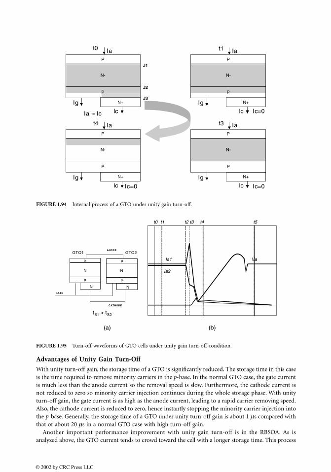
Advantages of Unity Gain Turn-Off
With unity turn-off gain, the storage time of a GTO is significantly reduced. The storage time in this caseis the time required to remove minority carriers in the p-base. In the normal GTO case, the gate currentis much less than the anode current so the removal speed is slow. Furthermore, the cathode current isnot reduced to zero so minority carrier injection continues during the whole storage phase. With unityturn-off gain, the gate current is as high as the anode current, leading to a rapid carrier removing speed.Also, the cathode current is reduced to zero, hence instantly stopping the minority carrier injection intothe p-base. Generally, the storage time of a GTO under unity turn-off gain is about 1 µs compared withthat of about 20 µs in a normal GTO case with high turn-off gain.
Another important performance improvement with unity gain turn-off is in the RBSOA. As isanalyzed above, the GTO current tends to crowd toward the cell with a longer storage time. This process
FIGURE 1.94 Internal process of a GTO under unity gain turn-off.
FIGURE 1.95 Turn-off waveforms of GTO cells under unity gain turn-off condition.
t0 t1
t3t4
P
N-
P
N+
Ia
IgIc
P
N-
P
N+
Ia
IgIc
P
N-
P
N+
Ia
IgIc
P
N-
P
N+
Ia
IgIc
Ia ≈ Ic Ic=0
Ic=0Ic=0
J1
J2
J3
P
N
P
N
ANODE
P
N
P
N
CATHODE
GATE
GTO1 GTO2
tS1 > tS2
(a)
Ia1
Ia2
t0 t2t1 t3 t4 t5
Va
(b)
© 2002 by CRC Press LLC
significantly limits the average instant power a GTO can withstand so a dV/dt snubber circuitry isnormally required to limit the voltage level, hence the instant power stress, during turn-off transition.
GTO cells under unity gain turn-off have a tendency toward uniform current sharing, hence large RBSOA.First, the current filamentation due to the difference of storage time is greatly reduced because the absolutestorage time is reduced to less than 1 µs. During the voltage rising phase after the storage time, if one cellstill shares more current, that cell will have a faster carrier extraction rate and hence will turn off thatcell faster. There is therefore a negative feedback process with current sharing instead of a positive one.This negative process is shown in Fig. 1.96.
With this uniform current distribution tendency provided by the unity turn-off gain, a GTO as a wholecan be assumed to be more uniform in current sharing and hence can withstand much higher averageinstant power during turn-off transition. The RBSOA should now be pushed toward a power constant of200 kW/cm
2 as predicted by Eq. (1.23) (in Section 1.8). This RBSOA is sufficiently large that a GTO should
be able to perform turn-off operation even without the help of a dV/dt snubber. It should also be pointedout again that the onset of dynamic avalanche may not be the actual RBSOA boundary because if it doesnot initiate a runaway current filament, it is not a destructive one. Experimental results [1] on IGCT turn-off, however, suggest that the dynamic avalanche is not uniform and that it does lead to failure of a device.Unity gain turn-off is therefore effective in removing any current filament problem associated with storage-time differences and the dynamic avalanche soon after the current filament is formed.
Hard-Driven GTOs
Unity turn-off gain can significantly improve the performance of a GTO in several aspects, includingRBSOA and turn-off storage time. Several innovative approaches have been proposed to realize unityturn-off gain. In all approaches, achieving unity turn-off gain is critical. This would require that cathodecurrent be commuted to the gate path very fast. To turn off a 4-kA GTO with unity gain, the commutationrate should be higher than 6 kA/µs. This high commutation rate requirement distinguishes the performanceof each of the devices discussed below. According to their realizations, they can be classified into twodifferent categories: hard-driven type and MOS-controlled type. Hard-driven type approaches use apowerful gate driver to realize unity turn-off gain. The gate driver supplies the gate current and the gatingpower. Falling in this category is the integrated gate commutated thyristor (IGCT) [2]. The MOS-controlled approaches use MOSFETs to aid the turn-off process of the GTO. Other than the unity turn-off gain, these approaches also save control power for the turn-off process. Falling in this category arethe emitter turn-off (ETO) [3] thyristor and the MOS turn-off (MTO) [4] thyristor.
IGCT
The key to achieving a hard-driven or unity-gain turn-off condition lies in the gate current commutationrate. A rate as high as 6 kA/µs is required for 4-kA turn-off. Two methods have been demonstrated for theimplementation of a hard-driven GTO. The first is to hold the gate loop inductance low enough (3 nH)that a DC gate voltage less than the breakdown voltage of the gate–cathode junction (18 to 22 V) cangenerate a slew rate of 6 kA/µs. This approach is used in the IGCT/GCT [2, 5] (IGCT is an ABB product,GCT is by Mitsubishi, but the concept is the same), where a special low-inductance GTO housing and a
FIGURE 1.96 Negative feedback mechanism in the current sharing of two paralleled GTO cells during voltageincreasing phase.
If Ia1>Ia2 Q1> Q2 x1> x2
Em1> Em2Ia1 , Ia2
negative feedback
∆V1> V2∆ ∆ ∆
∆ ∆ ∆ ∆
© 2002 by CRC Press LLC

carefully designed gate driver meet this requirement. The power consumption by the GCT driver is greatlyreduced compared with that of a conventional GTO driver, since the gate current is present for a muchshorter period of time [6]. Figure 1.97 shows the external view of the two commercially available GCTs.
The key disadvantage of the GCT approach is the high cost associated with the low-inductance housingdesign for the GTO and the low inductance and high current design for the gate driver.
MTO
Figure 1.98a shows the turn-off principle of a MTO™ [4, 7] developed by Silicon Power Corporation.The MTO device packages a number of low-voltage MOSFETs within a normal GTO device housing toform a current path that is in parallel with the emitter junction of the GTO. Therefore, the MTO looks
FIGURE 1.97 GCT operation principle and two GCTs developed by Mitsubishi and ABB. (Photographs courtesyof Mitsubishi (top) and ABB (bottom).)
LG ≤ 3nH
20 V
- +
GCT LG<3 Driver
Mitsubishi 4kA / 4.5 kV GCT
ABB 4 kA / 4.5 kV IGCT
© 2002 by CRC Press LLC
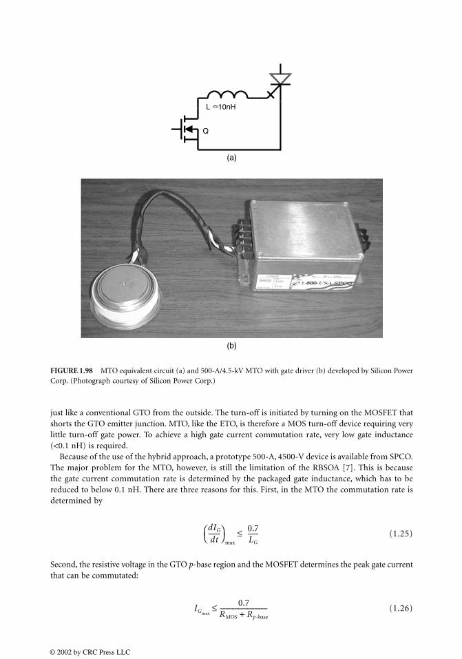
just like a conventional GTO from the outside. The turn-off is initiated by turning on the MOSFET thatshorts the GTO emitter junction. MTO, like the ETO, is therefore a MOS turn-off device requiring verylittle turn-off gate power. To achieve a high gate current commutation rate, very low gate inductance(<0.1 nH) is required.
Because of the use of the hybrid approach, a prototype 500-A, 4500-V device is available from SPCO.The major problem for the MTO, however, is still the limitation of the RBSOA [7]. This is becausethe gate current commutation rate is determined by the packaged gate inductance, which has to bereduced to below 0.1 nH. There are three reasons for this. First, in the MTO the commutation rate isdetermined by
(1.25)
Second, the resistive voltage in the GTO p-base region and the MOSFET determines the peak gate currentthat can be commutated:
(1.26)
FIGURE 1.98 MTO equivalent circuit (a) and 500-A/4.5-kV MTO with gate driver (b) developed by Silicon PowerCorp. (Photograph courtesy of Silicon Power Corp.)
(a)
L 10nH
Q
(b)
dIG
dt--------
max
0.7LG
-------≤
IGmax
0.7RMOS Rp-base+-------------------------------≤
© 2002 by CRC Press LLC

Third, since there is no reverse bias voltage applied to the GTO emitter junction in the MTO, it is veryeasy to become latched again. Snubberless turn-off capability of the MTO is therefore lower than theGCT and ETO.
ETO
The method to achieve unity gain in the ETO thyristor is to insert an additional switch in series withthe cathode of the GTO. The cathode of the GTO is the emitter of the internal npn transistor, so theseries switch is referred to as the emitter switch and the new device is termed ETO. Turning off the emitterswitch generates a high transient voltage long enough to commutate the emitter current to the gate patheven with a higher parasitic inductance present. Because of this higher tolerance for parasitic inductance,conventional GTOs can be used in the ETO. An additional switch is connected to the gate of the GTO,and is complementary to the emitter switch. These switches are implemented with many paralleled low-voltage, high-current MOSFETs to minimize the additional conduction loss due to the emitter switch.The typical value for the conduction loss due to the series switch is 0.2 V at the average GTO currentrating. The turn-off driving power for the ETO is negligible, since the turn-off is purely due to theremoval of a MOSFET gate signal. The ETO in many aspects is similar to the IGBT. For example, theturn-off mechanism used in IGBT is also an emitter turn-off, and the IGBT always turns off in the ruggedpnp transistor mode.
Figure 1.99 shows the equivalent circuit and hardware photograph of the developed 4-kA, 6-kV ETOby Virginia Tech. Other lower current rating ETOs have also been demonstrated by Virginia Tech. Becauseof the use of hybrid approach based on conventional GTO, ETO devices have clear advantages in termsof cost and gate drive power requirement over GCTs. ETO devices also have two other advantages whencompared with the GCT. One is its feasibility of having a FBSOA [3, 8], and the other is its simplicityin overcurrent protection [8].
Conclusions
These newly developed GTOs (IGCT, MTO, and ETO) all utilize the unity gain turn-off concept andhave dramatically improved performance compared with conventional GTOs. Quantitative comparisonsof these devices are provided in a separate section on high-power IGBTs (Section 1.9).
FIGURE 1.99 ETO equivalent circuit (a) and a 4-kA/6-kV ETO (b). An ETO gate driver is also shown.
© 2002 by CRC Press LLC
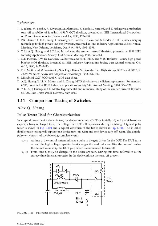
References
1. I. Takata, M. Bessho, K. Koyanagi, M. Akamatsu, K. Satoh, K. Kurachi, and T. Nakagawa, Snubberlessturn-off capability of four-inch 4.5k V GCT thyristor, presented at IEEE International Symposiumon Power Semiconductor Devices and Ics, 1998, 177–180.
2. P.K. Steimer, H.E. Gruning, J. Werninger, E. Carrol, S. Klaka, and S. Linder, IGCT—a new emergingtechnology for high power, low cost inverters, presented at IEEE Industry Applications Society AnnualMeeting, New Orleans, Louisiana, Oct. 5–9, 1997, 1592–1599.
3. Y. Li, A.Q. Huang, and F.C. Lee, Introducing the emitter turn-off thyristor, presented at 1998 IEEEIndustry Applications Society 33rd Annual Meeting, 1998, 860–864.
4. D.E. Piccone, R.W. De Doncker, J.A. Barrow, and W.H. Tobin, The MTO thyristor—a new high powerbipolar MOS thyristor, presented at IEEE Industry Applications Society 31st Annual Meeting, Oct.6–10, 1996, 1472–1473.
5. E.R. Motto and M. Yamamoto, New High Power Semiconductors: High Voltage IGBTs and GCTs, inPCIM’98 Power Electronics Conference Proceedings, 1998, 296–302.
6. Mitsubishi GCT FGC4000BX-90DS data sheet.7. A.Q. Huang, Y. Li, K. Motto, and B. Zhang, MTO thyristor—an efficient replacement for standard
GTO, presented at IEEE Industry Applications Society 34th Annual Meeting, 1990, 364–372.8. Y. Li, A.Q. Huang, and K. Motto, Experimental and numerical study of the emitter turn-off thyristor
(ETO), IEEE Trans. Power Electron., May 2000.
1.11 Comparison Testing of Switches
Alex Q. Huang
Pulse Tester Used for Characterization
In a typical power device dynamic test, the device under test (DUT) is initially off, and the high-voltagecapacitor bank is charged to set the voltage the DUT will experience during switching. A typical pulsetester is shown in Fig. 1.100 and a typical waveform of the test is shown in Fig. 1.101. The so-calleddouble pulse testing will capture one device turn-on event and one device turn-off event. The double-pulse test consists of the following complete events:
t0–t1: At time t0, the control system initiates a pulse to the gate driver for the DUT. The DUT turnson and the high voltage capacitor bank charges the load inductor. After the current reachesthe desired value at t1, the DUT gate driver is commanded to turn off.
t1–t2: From time t1 to t2, no changes to the device are seen. During this time, referred to as thestorage time, internal processes in the device initiate the turn-off process.
FIGURE 1.100 Pulse tester schematic diagram.
© 2002 by CRC Press LLC
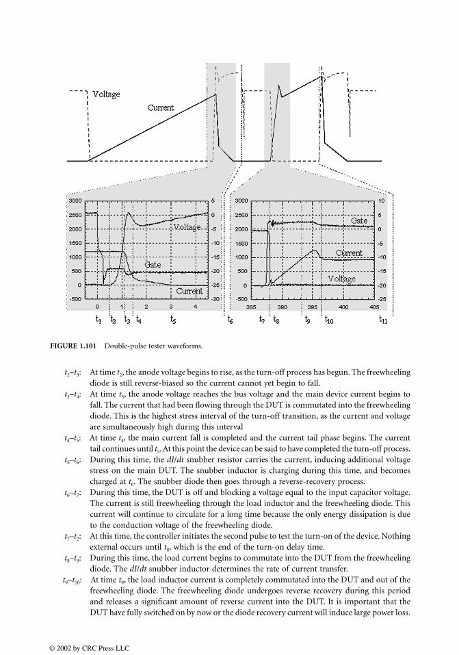
t2–t3: At time t2, the anode voltage begins to rise, as the turn-off process has begun. The freewheelingdiode is still reverse-biased so the current cannot yet begin to fall.
t3–t4: At time t3, the anode voltage reaches the bus voltage and the main device current begins tofall. The current that had been flowing through the DUT is commutated into the freewheelingdiode. This is the highest stress interval of the turn-off transition, as the current and voltageare simultaneously high during this interval
t4–t5: At time t4, the main current fall is completed and the current tail phase begins. The currenttail continues until t5. At this point the device can be said to have completed the turn-off process.
t5–t6: During this time, the dI/dt snubber resistor carries the current, inducing additional voltagestress on the main DUT. The snubber inductor is charging during this time, and becomescharged at t6. The snubber diode then goes through a reverse-recovery process.
t6–t7: During this time, the DUT is off and blocking a voltage equal to the input capacitor voltage.The current is still freewheeling through the load inductor and the freewheeling diode. Thiscurrent will continue to circulate for a long time because the only energy dissipation is dueto the conduction voltage of the freewheeling diode.
t7–t2: At this time, the controller initiates the second pulse to test the turn-on of the device. Nothingexternal occurs until t8, which is the end of the turn-on delay time.
t8–t9: During this time, the load current begins to commutate into the DUT from the freewheelingdiode. The dI/dt snubber inductor determines the rate of current transfer.
t9–t10: At time t9, the load inductor current is completely commutated into the DUT and out of thefreewheeling diode. The freewheeling diode undergoes reverse recovery during this periodand releases a significant amount of reverse current into the DUT. It is important that theDUT have fully switched on by now or the diode recovery current will induce large power loss.
FIGURE 1.101 Double-pulse tester waveforms.
© 2002 by CRC Press LLC
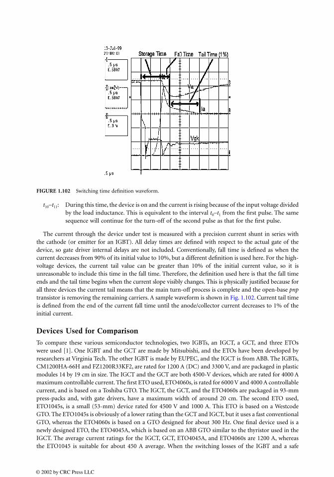
t10–t11: During this time, the device is on and the current is rising because of the input voltage dividedby the load inductance. This is equivalent to the interval t0–t1 from the first pulse. The samesequence will continue for the turn-off of the second pulse as that for the first pulse.
The current through the device under test is measured with a precision current shunt in series withthe cathode (or emitter for an IGBT). All delay times are defined with respect to the actual gate of thedevice, so gate driver internal delays are not included. Conventionally, fall time is defined as when thecurrent decreases from 90% of its initial value to 10%, but a different definition is used here. For the high-voltage devices, the current tail value can be greater than 10% of the initial current value, so it isunreasonable to include this time in the fall time. Therefore, the definition used here is that the fall timeends and the tail time begins when the current slope visibly changes. This is physically justified because forall three devices the current tail means that the main turn-off process is complete and the open-base pnptransistor is removing the remaining carriers. A sample waveform is shown in Fig. 1.102. Current tail timeis defined from the end of the current fall time until the anode/collector current decreases to 1% of theinitial current.
Devices Used for Comparison
To compare these various semiconductor technologies, two IGBTs, an IGCT, a GCT, and three ETOswere used [1]. One IGBT and the GCT are made by Mitsubishi, and the ETOs have been developed byresearchers at Virginia Tech. The other IGBT is made by EUPEC, and the IGCT is from ABB. The IGBTs,CM1200HA-66H and FZ1200R33KF2, are rated for 1200 A (DC) and 3300 V, and are packaged in plasticmodules 14 by 19 cm in size. The IGCT and the GCT are both 4500-V devices, which are rated for 4000 Amaximum controllable current. The first ETO used, ETO4060s, is rated for 6000 V and 4000 A controllablecurrent, and is based on a Toshiba GTO. The IGCT, the GCT, and the ETO4060s are packaged in 93-mmpress-packs and, with gate drivers, have a maximum width of around 20 cm. The second ETO used,ETO1045s, is a small (53-mm) device rated for 4500 V and 1000 A. This ETO is based on a WestcodeGTO. The ETO1045s is obviously of a lower rating than the GCT and IGCT, but it uses a fast conventionalGTO, whereas the ETO4060s is based on a GTO designed for about 300 Hz. One final device used is anewly designed ETO, the ETO4045A, which is based on an ABB GTO similar to the thyristor used in theIGCT. The average current ratings for the IGCT, GCT, ETO4045A, and ETO4060s are 1200 A, whereasthe ETO1045 is suitable for about 450 A average. When the switching losses of the IGBT and a safe
FIGURE 1.102 Switching time definition waveform.
© 2002 by CRC Press LLC
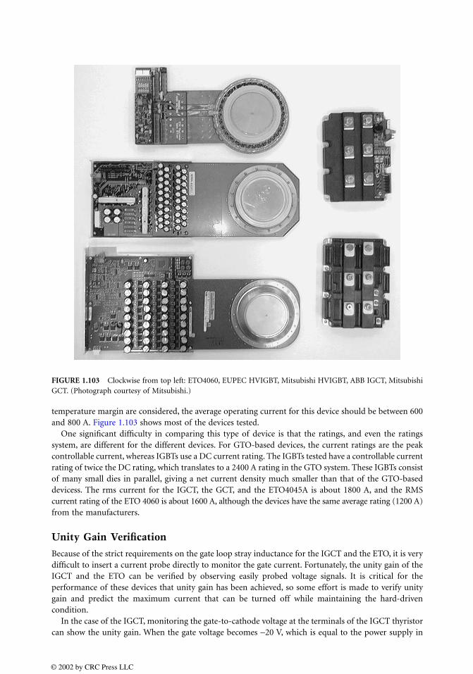
temperature margin are considered, the average operating current for this device should be between 600and 800 A. Figure 1.103 shows most of the devices tested.
One significant difficulty in comparing this type of device is that the ratings, and even the ratingssystem, are different for the different devices. For GTO-based devices, the current ratings are the peakcontrollable current, whereas IGBTs use a DC current rating. The IGBTs tested have a controllable currentrating of twice the DC rating, which translates to a 2400 A rating in the GTO system. These IGBTs consistof many small dies in parallel, giving a net current density much smaller than that of the GTO-baseddevicess. The rms current for the IGCT, the GCT, and the ETO4045A is about 1800 A, and the RMScurrent rating of the ETO 4060 is about 1600 A, although the devices have the same average rating (1200 A)from the manufacturers.
Unity Gain Verification
Because of the strict requirements on the gate loop stray inductance for the IGCT and the ETO, it is verydifficult to insert a current probe directly to monitor the gate current. Fortunately, the unity gain of theIGCT and the ETO can be verified by observing easily probed voltage signals. It is critical for theperformance of these devices that unity gain has been achieved, so some effort is made to verify unitygain and predict the maximum current that can be turned off while maintaining the hard-drivencondition.
In the case of the IGCT, monitoring the gate-to-cathode voltage at the terminals of the IGCT thyristorcan show the unity gain. When the gate voltage becomes −20 V, which is equal to the power supply in
FIGURE 1.103 Clockwise from top left: ETO4060, EUPEC HVIGBT, Mitsubishi HVIGBT, ABB IGCT, MitsubishiGCT. (Photograph courtesy of Mitsubishi.)
© 2002 by CRC Press LLC
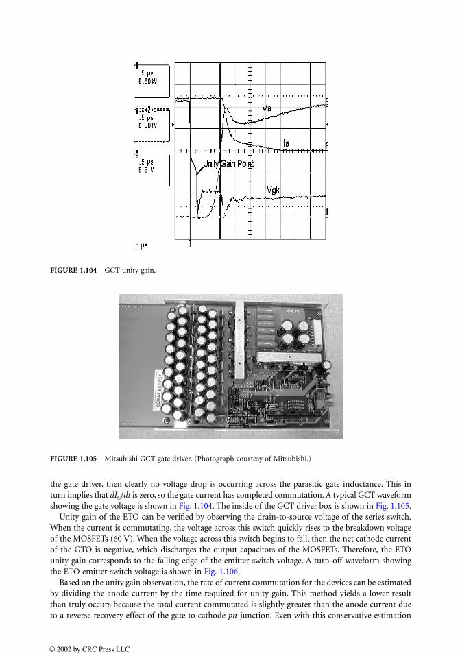
the gate driver, then clearly no voltage drop is occurring across the parasitic gate inductance. This inturn implies that dIG/dt is zero, so the gate current has completed commutation. A typical GCT waveformshowing the gate voltage is shown in Fig. 1.104. The inside of the GCT driver box is shown in Fig. 1.105.
Unity gain of the ETO can be verified by observing the drain-to-source voltage of the series switch.When the current is commutating, the voltage across this switch quickly rises to the breakdown voltageof the MOSFETs (60 V). When the voltage across this switch begins to fall, then the net cathode currentof the GTO is negative, which discharges the output capacitors of the MOSFETs. Therefore, the ETOunity gain corresponds to the falling edge of the emitter switch voltage. A turn-off waveform showingthe ETO emitter switch voltage is shown in Fig. 1.106.
Based on the unity gain observation, the rate of current commutation for the devices can be estimatedby dividing the anode current by the time required for unity gain. This method yields a lower resultthan truly occurs because the total current commutated is slightly greater than the anode current dueto a reverse recovery effect of the gate to cathode pn-junction. Even with this conservative estimation
FIGURE 1.104 GCT unity gain.
FIGURE 1.105 Mitsubishi GCT gate driver. (Photograph courtesy of Mitsubishi.)
© 2002 by CRC Press LLC
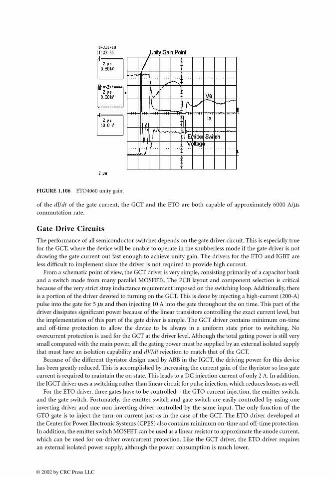
of the dI/dt of the gate current, the GCT and the ETO are both capable of approximately 6000 A/µscommutation rate.
Gate Drive Circuits
The performance of all semiconductor switches depends on the gate driver circuit. This is especially truefor the GCT, where the device will be unable to operate in the snubberless mode if the gate driver is notdrawing the gate current out fast enough to achieve unity gain. The drivers for the ETO and IGBT areless difficult to implement since the driver is not required to provide high current.
From a schematic point of view, the GCT driver is very simple, consisting primarily of a capacitor bankand a switch made from many parallel MOSFETs. The PCB layout and component selection is criticalbecause of the very strict stray inductance requirement imposed on the switching loop. Additionally, thereis a portion of the driver devoted to turning on the GCT. This is done by injecting a high-current (200-A)pulse into the gate for 5 µs and then injecting 10 A into the gate throughout the on time. This part of thedriver dissipates significant power because of the linear transistors controlling the exact current level, butthe implementation of this part of the gate driver is simple. The GCT driver contains minimum on-timeand off-time protection to allow the device to be always in a uniform state prior to switching. Noovercurrent protection is used for the GCT at the driver level. Although the total gating power is still verysmall compared with the main power, all the gating power must be supplied by an external isolated supplythat must have an isolation capability and dV/dt rejection to match that of the GCT.
Because of the different thyristor design used by ABB in the IGCT, the driving power for this devicehas been greatly reduced. This is accomplished by increasing the current gain of the thyristor so less gatecurrent is required to maintain the on state. This leads to a DC injection current of only 2 A. In addition,the IGCT driver uses a switching rather than linear circuit for pulse injection, which reduces losses as well.
For the ETO driver, three gates have to be controlled—the GTO current injection, the emitter switch,and the gate switch. Fortunately, the emitter switch and gate switch are easily controlled by using oneinverting driver and one non-inverting driver controlled by the same input. The only function of theGTO gate is to inject the turn-on current just as in the case of the GCT. The ETO driver developed atthe Center for Power Electronic Systems (CPES) also contains minimum on-time and off-time protection.In addition, the emitter switch MOSFET can be used as a linear resistor to approximate the anode current,which can be used for on-driver overcurrent protection. Like the GCT driver, the ETO driver requiresan external isolated power supply, although the power consumption is much lower.
FIGURE 1.106 ETO4060 unity gain.
© 2002 by CRC Press LLC
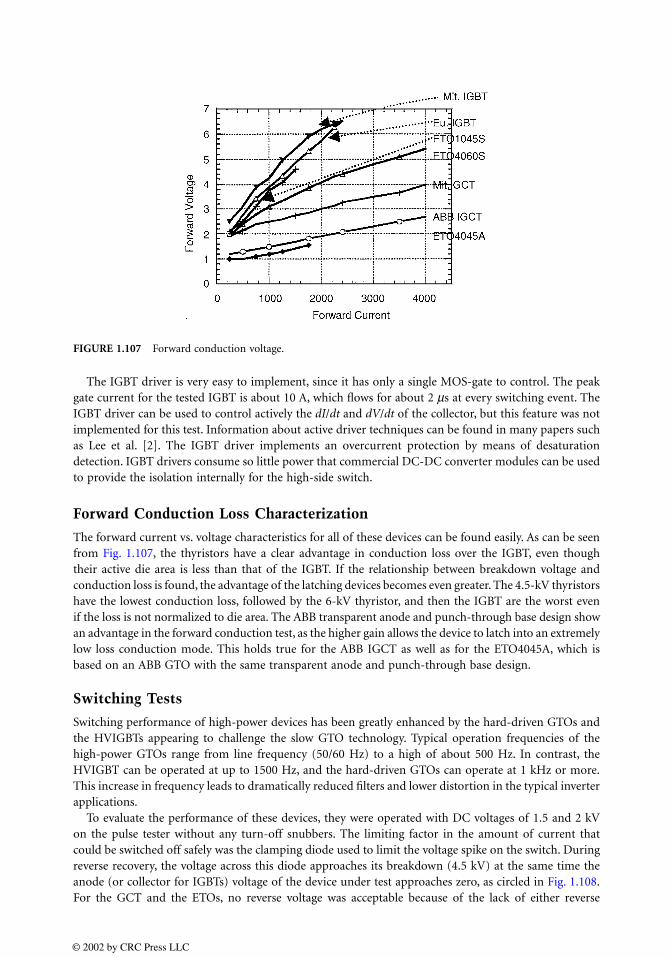
The IGBT driver is very easy to implement, since it has only a single MOS-gate to control. The peakgate current for the tested IGBT is about 10 A, which flows for about 2 µs at every switching event. TheIGBT driver can be used to control actively the dI/dt and dV/dt of the collector, but this feature was notimplemented for this test. Information about active driver techniques can be found in many papers suchas Lee et al. [2]. The IGBT driver implements an overcurrent protection by means of desaturationdetection. IGBT drivers consume so little power that commercial DC-DC converter modules can be usedto provide the isolation internally for the high-side switch.
Forward Conduction Loss Characterization
The forward current vs. voltage characteristics for all of these devices can be found easily. As can be seenfrom Fig. 1.107, the thyristors have a clear advantage in conduction loss over the IGBT, even thoughtheir active die area is less than that of the IGBT. If the relationship between breakdown voltage andconduction loss is found, the advantage of the latching devices becomes even greater. The 4.5-kV thyristorshave the lowest conduction loss, followed by the 6-kV thyristor, and then the IGBT are the worst evenif the loss is not normalized to die area. The ABB transparent anode and punch-through base design showan advantage in the forward conduction test, as the higher gain allows the device to latch into an extremelylow loss conduction mode. This holds true for the ABB IGCT as well as for the ETO4045A, which isbased on an ABB GTO with the same transparent anode and punch-through base design.
Switching Tests
Switching performance of high-power devices has been greatly enhanced by the hard-driven GTOs andthe HVIGBTs appearing to challenge the slow GTO technology. Typical operation frequencies of thehigh-power GTOs range from line frequency (50/60 Hz) to a high of about 500 Hz. In contrast, theHVIGBT can be operated at up to 1500 Hz, and the hard-driven GTOs can operate at 1 kHz or more.This increase in frequency leads to dramatically reduced filters and lower distortion in the typical inverterapplications.
To evaluate the performance of these devices, they were operated with DC voltages of 1.5 and 2 kVon the pulse tester without any turn-off snubbers. The limiting factor in the amount of current thatcould be switched off safely was the clamping diode used to limit the voltage spike on the switch. Duringreverse recovery, the voltage across this diode approaches its breakdown (4.5 kV) at the same time theanode (or collector for IGBTs) voltage of the device under test approaches zero, as circled in Fig. 1.108.For the GCT and the ETOs, no reverse voltage was acceptable because of the lack of either reverse
FIGURE 1.107 Forward conduction voltage.
© 2002 by CRC Press LLC
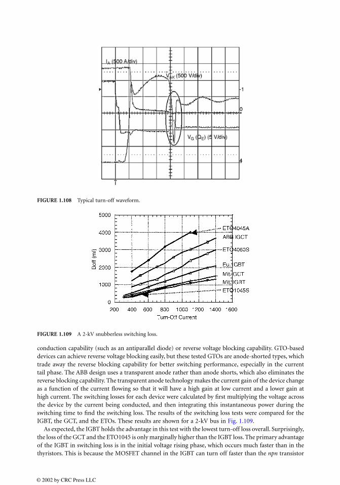
conduction capability (such as an antiparallel diode) or reverse voltage blocking capability. GTO-baseddevices can achieve reverse voltage blocking easily, but these tested GTOs are anode-shorted types, whichtrade away the reverse blocking capability for better switching performance, especially in the currenttail phase. The ABB design uses a transparent anode rather than anode shorts, which also eliminates thereverse blocking capability. The transparent anode technology makes the current gain of the device changeas a function of the current flowing so that it will have a high gain at low current and a lower gain athigh current. The switching losses for each device were calculated by first multiplying the voltage acrossthe device by the current being conducted, and then integrating this instantaneous power during theswitching time to find the switching loss. The results of the switching loss tests were compared for theIGBT, the GCT, and the ETOs. These results are shown for a 2-kV bus in Fig. 1.109.
As expected, the IGBT holds the advantage in this test with the lowest turn-off loss overall. Surprisingly,the loss of the GCT and the ETO1045 is only marginally higher than the IGBT loss. The primary advantageof the IGBT in switching loss is in the initial voltage rising phase, which occurs much faster than in thethyristors. This is because the MOSFET channel in the IGBT can turn off faster than the npn transistor
FIGURE 1.108 Typical turn-off waveform.
FIGURE 1.109 A 2-kV snubberless switching loss.
© 2002 by CRC Press LLC
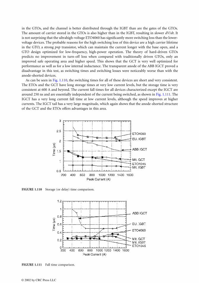
in the GTOs, and the channel is better distributed through the IGBT than are the gates of the GTOs.The amount of carrier stored in the GTOs is also higher than in the IGBT, resulting in slower dV/dt. Itis not surprising that the ultrahigh-voltage ETO4060 has significantly more switching loss than the lower-voltage devices. The probable reasons for the high switching loss of this device are a high carrier lifetimein the GTO, a strong pnp transistor, which can maintain the current longer with the base open, and aGTO design optimized for low-frequency, high-power operation. The theory of hard-driven GTOspredicts no improvement in turn-off loss when compared with traditionally driven GTOs, only animproved safe operating area and higher speed. This shows that the GCT is very well optimized forperformance as well as for a low internal inductance. The transparent anode of the ABB IGCT proved adisadvantage in this test, as switching times and switching losses were noticeably worse than with theanode-shorted devices.
As can be seen in Fig. 1.110, the switching times for all of these devices are short and very consistent.The ETOs and the GCT have long storage times at very low current levels, but the storage time is veryconsistent at 600 A and beyond. The current fall times for all devices characterized except the IGCT arearound 250 ns and are essentially independent of the current being switched, as shown in Fig. 1.111. TheIGCT has a very long current fall time at low current levels, although the speed improves at highercurrents. The IGCT tail has a very large magnitude, which again shows that the anode-shorted structureof the GCT and the ETOs offers advantages in this area.
FIGURE 1.110 Storage (or delay) time comparison.
FIGURE 1.111 Fall time comparison.
© 2002 by CRC Press LLC
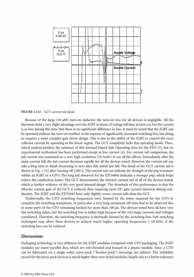
Because of the large (10 µH) turn-on inductor, the turn-on loss for all devices is negligible. All thethyristors hold a very slight advantage over the IGBT in terms of voltage fall time at turn-on, but the currentis so low during this time that there is no significant difference in loss. It must be noted that the IGBT canbe operated without the turn-on snubber at the expense of significantly increased switching loss, but doingso requires a more complex gate driver design. This is due to the ability of the IGBT to control the exactcollector current by operating in the linear region. The GCT completely lacks this operating mode. Theo-retical analysis predicts the existence of this forward-biased Safe Operating Area for the ETO [3], but noexperimental verification has been performed except at low current [4]. For current tail comparison, thetail current was examined on a very high resolution (10 A/div) to see all the effects. Immediately after themain current fall, the tail current decreases rapidly for all the devices tested. However, the current tail cantake a long time to finish decreasing to zero after this initial fast fall. The detail of the GCT current tail isshown in Fig. 1.112 after turning off 1200 A. The current tail can indicate the strength of the pnp transistorwithin an IGBT or a GTO. The long tail observed for the ETO4060 indicates a stronger pnp, which helpsreduce the conduction losses. The GCT demonstrates the shortest current tail of all of the devices tested,which is further evidence of the very good internal design. The drawback of this performance is that theeffective current gain of the GCT is reduced, thus requiring more DC gate current injection during con-duction. The IGBT and the ETO1045 have only slightly worse current tails than the GCT.
Traditionally, the GTO switching frequencies were limited by the times required for the GTO tocomplete the switching transitions. In particular, a very long minimum off-time had to be observed dueto some parts of the GTO remaining latched for more than 100 µs. The devices tested here all have veryfast switching times, but the switching loss is rather high because of the very large currents and voltagesconsidered. Therefore, the switching frequency is thermally limited by the switching loss. Soft switchingtechniques may allow these devices to achieve much higher operating frequencies (∼10 kHz) if theswitching loss can be reduced.
Discussion
Packaging technology is very different for the IGBT modules compared with GTO packaging. The IGBTmodules use many parallel dies, which are wire-bonded and housed in a plastic module. Since a GTOcan be fabricated on a single wafer, press-pack (“hockey-puck”) housings are utilized. The reliabilityrecord for the press-pack devices is much higher than wire-bond modules, largely due to a better tolerance
FIGURE 1.112 GCT current tail detail.
© 2002 by CRC Press LLC
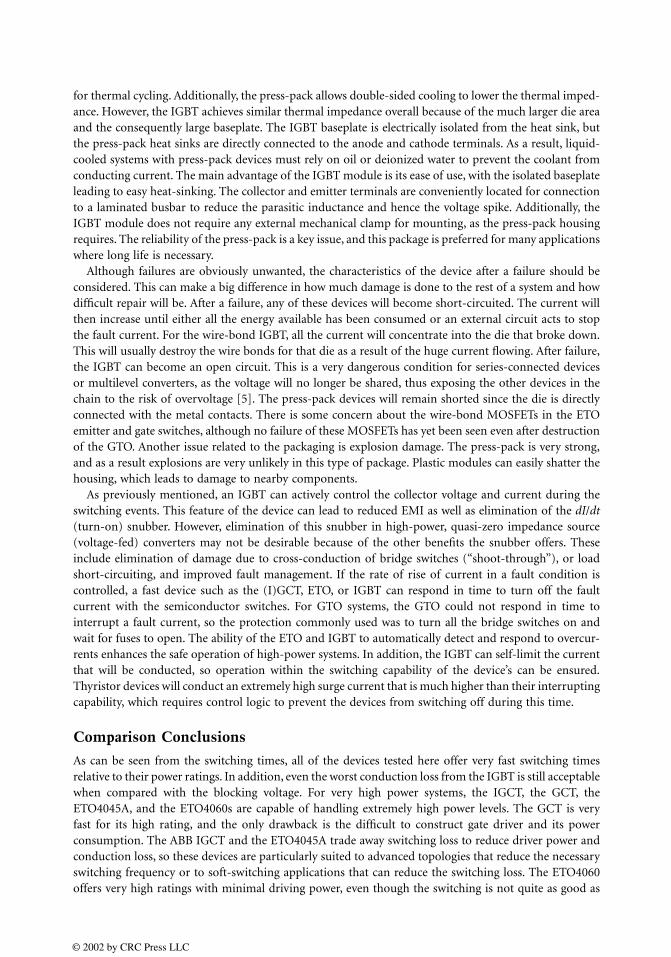
for thermal cycling. Additionally, the press-pack allows double-sided cooling to lower the thermal imped-ance. However, the IGBT achieves similar thermal impedance overall because of the much larger die areaand the consequently large baseplate. The IGBT baseplate is electrically isolated from the heat sink, butthe press-pack heat sinks are directly connected to the anode and cathode terminals. As a result, liquid-cooled systems with press-pack devices must rely on oil or deionized water to prevent the coolant fromconducting current. The main advantage of the IGBT module is its ease of use, with the isolated baseplateleading to easy heat-sinking. The collector and emitter terminals are conveniently located for connectionto a laminated busbar to reduce the parasitic inductance and hence the voltage spike. Additionally, theIGBT module does not require any external mechanical clamp for mounting, as the press-pack housingrequires. The reliability of the press-pack is a key issue, and this package is preferred for many applicationswhere long life is necessary.
Although failures are obviously unwanted, the characteristics of the device after a failure should beconsidered. This can make a big difference in how much damage is done to the rest of a system and howdifficult repair will be. After a failure, any of these devices will become short-circuited. The current willthen increase until either all the energy available has been consumed or an external circuit acts to stopthe fault current. For the wire-bond IGBT, all the current will concentrate into the die that broke down.This will usually destroy the wire bonds for that die as a result of the huge current flowing. After failure,the IGBT can become an open circuit. This is a very dangerous condition for series-connected devicesor multilevel converters, as the voltage will no longer be shared, thus exposing the other devices in thechain to the risk of overvoltage [5]. The press-pack devices will remain shorted since the die is directlyconnected with the metal contacts. There is some concern about the wire-bond MOSFETs in the ETOemitter and gate switches, although no failure of these MOSFETs has yet been seen even after destructionof the GTO. Another issue related to the packaging is explosion damage. The press-pack is very strong,and as a result explosions are very unlikely in this type of package. Plastic modules can easily shatter thehousing, which leads to damage to nearby components.
As previously mentioned, an IGBT can actively control the collector voltage and current during theswitching events. This feature of the device can lead to reduced EMI as well as elimination of the dI/dt(turn-on) snubber. However, elimination of this snubber in high-power, quasi-zero impedance source(voltage-fed) converters may not be desirable because of the other benefits the snubber offers. Theseinclude elimination of damage due to cross-conduction of bridge switches (“shoot-through”), or loadshort-circuiting, and improved fault management. If the rate of rise of current in a fault condition iscontrolled, a fast device such as the (I)GCT, ETO, or IGBT can respond in time to turn off the faultcurrent with the semiconductor switches. For GTO systems, the GTO could not respond in time tointerrupt a fault current, so the protection commonly used was to turn all the bridge switches on andwait for fuses to open. The ability of the ETO and IGBT to automatically detect and respond to overcur-rents enhances the safe operation of high-power systems. In addition, the IGBT can self-limit the currentthat will be conducted, so operation within the switching capability of the device’s can be ensured.Thyristor devices will conduct an extremely high surge current that is much higher than their interruptingcapability, which requires control logic to prevent the devices from switching off during this time.
Comparison Conclusions
As can be seen from the switching times, all of the devices tested here offer very fast switching timesrelative to their power ratings. In addition, even the worst conduction loss from the IGBT is still acceptablewhen compared with the blocking voltage. For very high power systems, the IGCT, the GCT, theETO4045A, and the ETO4060s are capable of handling extremely high power levels. The GCT is veryfast for its high rating, and the only drawback is the difficult to construct gate driver and its powerconsumption. The ABB IGCT and the ETO4045A trade away switching loss to reduce driver power andconduction loss, so these devices are particularly suited to advanced topologies that reduce the necessaryswitching frequency or to soft-switching applications that can reduce the switching loss. The ETO4060offers very high ratings with minimal driving power, even though the switching is not quite as good as
© 2002 by CRC Press LLC

the GCT; however, it is better than the IGCT. The IGBT offers the best switching speed and loss of anyof the devices tested and the simplest drive. However, the GCT and small ETO are amazingly close tothe IGBT in switching loss considering their latching nature and nearly 50% higher voltage rating. Theperformance of all devices tested here is very good, especially compared with the conventional GTOapplications.
References
1. K. Motto, Y. Li, and A.Q. Huang, Comparison of the state-of-the-art in high power IGBTs, IGCTs,and ETOs, in Conf. Rec. IEEE-APEC, 2000, 1129–1136.
2. H.-G. Lee, Y.-H. Lee, B.-S. Suh, and D.-S. Hyun, An improved gate control scheme for snubberlessoperation of high power IGBTs, in Conf. Rec. IEEE-IAS, 1997, 975–982.
3. Y. Li, A.Q. Huang, and K. Motto, Experimental and numerical study of the Emitter Turn-Off thyristor(ETO), IEEE Trans. Power Electron., 15(3), 2000, 561–574.
4. Z. Xu, Y. Bai, Y. Li, and A.Q. Huang, Experimental demonstration of the forward biased safe operationarea of the emitter turn-off thyristor, in Proc. CPES-VT Seminar, 2000, 448–455.
5. S. Bernet, R. Teichmann, A. Zuckerberger, and P. Steimer, Comparison of high power IGBTs and harddriven GTOs for high power inverters, in Conf. Rec. IEEE-APEC, 1998, 711–718.
© 2002 by CRC Press LLC

© 2002 by CRC Press LLC
II
Power Electronic Circuits and
Controls
2 DC-DC Converters
Richard Wies, Bipin Satavalekar, Ashish Agrawal, Javad Mahdavi, Ali Agah, Ali Emadi, Daniel Jeffrey Shortt
Overview • Choppers • Buck Converters • Boost Converters •Cúk Converter • Buck–Boost Converters
3 AC-AC Conversion
Sándor Halász
Introduction • Cycloconverters • Matrix Converters
4 Rectifiers
Sam Guccione, Mahesh M. Swamy, Ana Stankovic
Uncontrolled Single-Phase Rectifiers • Uncontrolled and Controlled Rectifiers • Three-Phase Pulse-Width-Modulated Boost-Type Rectifiers
5 Inverters
Michael Giesselmann, Attila Karpati, István Nagy, Dariusz Czarkowski, Michael E. Ropp
Overview • DC-AC Conversion • Resonant Converters • Series-ResonantInverters • Resonant DC-Link Inverters • Auxiliary Resonant Commutated Pole Inverters
6 Multilevel Converters
Keith Corzine
Introduction • Multilevel Voltage Source Modulation • Fundamental Multilevel ConverterTopologies • Cascaded Multilevel Converter Topologies • Multilevel Converter LaboratoryExamples • Conclusions
7 Modulation Strategies
Michael Giesselmann, Hossein Salehfar, Hamid A. Toliyat, Tahmid Ur Rahman
Introduction • Six-Step Modulation • Pulse Width Modulation • Third Harmonic Injectionfor Voltage Boost of SPWM Signals • Generation of PWM Signals Using Microcontrollersand DSPs • Voltage Source–Based Current Regulation • Hysteresis Feedback Control •Space-Vector Pulse Width Modulation
8 Sliding-Mode Control of Switched-Model Power Supplies
Giorgio Spiazzi, Paolo
Mattavelli
Introduction • Introduction to Sliding-Mode Control • Basics of Sliding-Mode Theory •Application of Sliding-Mode Control to DC-DC Converters—Basic Principle • Sliding-ModeControl of Buck DC-DC Converters • Extension to Boost and Buck–Boost DC-DC Converters •Extension to Cúk and SEPIC DC-DC Converters • General-Purpose Sliding-Mode ControlImplementation • Conclusions

2DC-DC Converters
2.1 OverviewReferences
2.2 ChoppersOne-Quadrant Choppers • Two-Quadrant Choppers •Four-Quadrant Choppers
2.3 Buck Converters Ideal Buck Circuit • Continuous-Conduction Mode • Discontinuous-Conduction Mode • References
2.4 Boost ConvertersIdeal Boost Circuit • Continuous-Conduction Mode • Discontinuous-Conduction Mode • References
2.5 Cúk Converter Nonisolated Operation • Practical Cúk Converter •References
2.6 Buck–Boost ConvertersCircuit-Analysis • Small Signal Transfer Functions • Component Selection • Flyback Power Stage •Summary • References
2.1 Overview
Richard Wies, Bipin Satavalekar, and Ashish Agrawal
The purpose of a DC-DC converter is to supply a regulated DC output voltage to a variable-load resistancefrom a fluctuating DC input voltage. In many cases the DC input voltage is obtained by rectifying a linevoltage that is changing in magnitude. DC-DC converters are commonly used in applications requiringregulated DC power, such as computers, medical instrumentation, communication devices, televisionreceivers, and battery chargers [1, 2]. DC-DC converters are also used to provide a regulated variableDC voltage for DC motor speed control applications.
The output voltage in DC-DC converters is generally controlled using a switching concept, as illustratedby the basic DC-DC converter shown in Fig. 2.1. Early DC-DC converters were known as choppers withsilicon-controlled rectifiers (SCRs) used as the switching mechanisms. Modern DC-DC converters clas-sified as switch mode power supplies (SMPS) employ insulated gate bipolar transistors (IGBTs) and metaloxide silicon field effect transistors (MOSFETs).
The switch mode power supply has several functions [3]:
1. Step down an unregulated DC input voltage to produce a regulated DC output voltage using abuck or step-down converter.
2. Step up an unregulated DC input voltage to produce a regulated DC output voltage using a boostor step-up converter.
Richard WiesUniversity of Alaska Fairbanks
Bipin SatavalekarUniversity of Alaska Fairbanks
Ashish AgrawalUniversity of Alaska Fairbanks
Javad MahdaviSharif University of Technology
Ali AgahSharif University of Technology
Ali EmadiIllinois Institute of Technology
Daniel Jeffrey ShorttCedarville University
© 2002 by CRC Press LLC
3. Step down and then step up an unregulated DC input voltage to produce a regulated DC outputvoltage using a buck–boost converter.
4. Invert the DC input voltage using a Cúk converter. 5. Produce multiple DC outputs using a combination of SMPS topologies.
The regulation of the average output voltage in a DC-DC converter is a function of the on-time ton of theswitch, the pulse width, and the switching frequency fs as illustrated in Fig. 2.2. Pulse width modulation(PWM) is the most widely used method of controlling the output voltage. The PWM concept is illustratedin Fig. 2.3. The output voltage control depends on the duty ratio D. The duty ratio is defined as
(2.1)
based on the on-time ton of the switch and the switching period Ts . PWM switching involves comparingthe level of a control voltage vcontrol to the level of a repetitive waveform as illustrated in Fig. 2.3 [2]. Theon-time of the switch is defined as the portion of the switching period where the value of the repetitive
FIGURE 2.1 Basic DC-DC converter.
FIGURE 2.2 DC-DC converter voltage waveforms.(From Mohan, N., Undeland, T. M., and Robbins, W. P.,Power Electronics: Converters, Applications, and Design,2nd ed., John Wiley & Sons, New York, 1995. With per-mission from John Wiley & Sons.)
FIGURE 2.3 Pulsewidth modulation concept. (From Mohan, N., Undeland, T. M., and Robbins, W. P., PowerElectronics: Converters, Applications, and Design, 2nd ed., John Wiley & Sons, New York, 1995. With permission fromJohn Wiley & Sons.)
S
+ +
Vi VoR
vo,i
Vi Vo
toffton t
Ts
ON ONON
OFF OFF t
vcontrol
Ts
vrepetitive
Vrepetitive
Dton
Ts
------vcontrol
Vrepetitive
------------------= =
© 2002 by CRC Press LLC

waveform is less than the control voltage. The switching period (switching frequency) remains constantwhile the control voltage level is adjusted to change the on-time and therefore the duty ratio of the switch.The switching frequency is usually chosen above 20 kHz so the noise is outside the audio range [2, 3].
DC-DC converters operate in one of two modes depending on the characteristics of the output current[1, 2]:
1. Continuous conduction 2. Discontinuous conduction
The continuous-conduction mode is defined by continuous output current (greater than zero) over theentire switching period, whereas the discontinuous conduction mode is defined by discontinuous outputcurrent (equal to zero) during any portion of the switching period. Each mode is discussed in relationshipto the buck and boost converters in subsequent sections.
References
1. Agrawal, J. P., Power Electronics Systems: Theory and Design, Prentice-Hall, Upper Saddle River, NJ,2001, chap. 6.
2. Mohan, N., Undeland, T. M., and Robbins, W. P., Power Electronics: Converters, Applications, andDesign, 2nd ed., John Wiley & Sons, New York, 1995, chap. 7.
3. Venkat, R., Switch Mode Power Supply, University of Technology, Sydney, Australia, March 1, 2001,available at http://www.ee.uts.edu.au/~venkat/pe_html/pe07_nc8.htm.
2.2 Choppers
Javad Mahdavi, Ali Agah, and Ali Emadi
Choppers are DC-DC converters that are used for transferring electrical energy from a DC source intoanother DC source, which may be a passive load. These converters are widely used in regulated switchingpower supplies and DC motor drive applications.
DC-DC converters that are discussed in this section are one-quadrant, two-quadrant, and four-quadrantchoppers. Step-down (buck) converter and step-up (boost) converters are basic one-quadrant convertertopologies. The two-quadrant chopper, which, in fact, is a current reversible converter, is the combinationof the two basic topologies. The full-bridge converter is derived from the step-down converter.
One-Quadrant Choppers
In one-quadrant choppers, the average DC output voltage is usually kept at a desired level, as there arefluctuations in input voltage and output load. These choppers operate only in first quadrant of v–i plane.In fact, output and input voltages and currents are always positive. Therefore, these converters are calledone-quadrant choppers.
One method of controlling the output voltage employs switching at a constant frequency, i.e., a constantswitching time period (T = ton + toff), and adjusting the on-duration of the switch to control the averageoutput voltage. In this method, which is called pulse-width modulation (PWM), the switch duty ratio dis defined as the ratio of the on-duration to the switching time period.
(2.2)
In the other control method, both the switching frequency and the on-duration of the switch arevaried. This method is mainly used in converters with force-commutated thyristors.
dton
T------=
© 2002 by CRC Press LLC
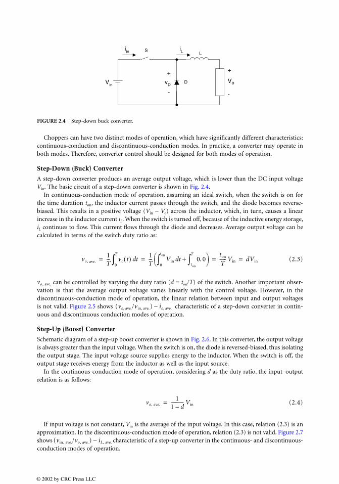
Choppers can have two distinct modes of operation, which have significantly different characteristics:continuous-conduction and discontinuous-conduction modes. In practice, a converter may operate inboth modes. Therefore, converter control should be designed for both modes of operation.
Step-Down (Buck) Converter
A step-down converter produces an average output voltage, which is lower than the DC input voltageVin. The basic circuit of a step-down converter is shown in Fig. 2.4.
In continuous-conduction mode of operation, assuming an ideal switch, when the switch is on forthe time duration ton, the inductor current passes through the switch, and the diode becomes reverse-biased. This results in a positive voltage (Vin − Vo) across the inductor, which, in turn, causes a linearincrease in the inductor current iL. When the switch is turned off, because of the inductive energy storage,iL continues to flow. This current flows through the diode and decreases. Average output voltage can becalculated in terms of the switch duty ratio as:
(2.3)
can be controlled by varying the duty ratio (d = ton/T) of the switch. Another important obser-vation is that the average output voltage varies linearly with the control voltage. However, in thediscontinuous-conduction mode of operation, the linear relation between input and output voltagesis not valid. Figure 2.5 shows characteristic of a step-down converter in contin-uous and discontinuous conduction modes of operation.
Step-Up (Boost) Converter
Schematic diagram of a step-up boost converter is shown in Fig. 2.6. In this converter, the output voltageis always greater than the input voltage. When the switch is on, the diode is reversed-biased, thus isolatingthe output stage. The input voltage source supplies energy to the inductor. When the switch is off, theoutput stage receives energy from the inductor as well as the input source.
In the continuous-conduction mode of operation, considering d as the duty ratio, the input–outputrelation is as follows:
(2.4)
If input voltage is not constant, Vin is the average of the input voltage. In this case, relation (2.3) is anapproximation. In the discontinuous-conduction mode of operation, relation (2.3) is not valid. Figure 2.7shows characteristic of a step-up converter in the continuous- and discontinuous-conduction modes of operation.
FIGURE 2.4 Step-down buck converter.
Vin
+
-
iL
D
Siin
vD
+
-
L
Vo
vo , ave.1T--- vo t( ) td
0
T
∫ 1T--- Vin td 0. 0
ton
T
∫+0
ton
∫ ton
T------ Vin dVin= = = =
vo , ave.
(vo ave., /vin ave., ) io ave.,–
vo , ave.1
1 d–----------- Vin=
(vin, ave./vo , ave.) iL , ave.–
© 2002 by CRC Press LLC
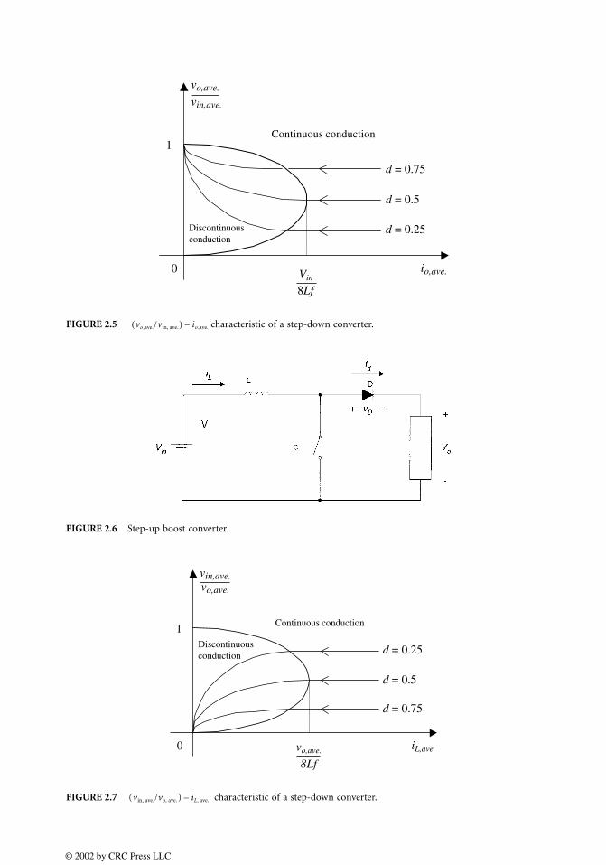
FIGURE 2.5 characteristic of a step-down converter.
FIGURE 2.6 Step-up boost converter.
FIGURE 2.7 characteristic of a step-down converter.
vin,ave.
vo,ave.
1
0
Continuous conduction
Discontinuousconduction
8LfVin
io,ave.
d = 0.25
d = 0.5
d = 0.75
vo ,ave./vin, ave.( ) io ,ave.–
vin,ave.vo,ave.
iL,ave.vo,ave.
1
0
Continuous conduction
Discontinuousconduction
d = 0.75
d = 0.5
d = 0.25
8Lf
(vin ave., /vo ave., ) iL ave.,–
© 2002 by CRC Press LLC
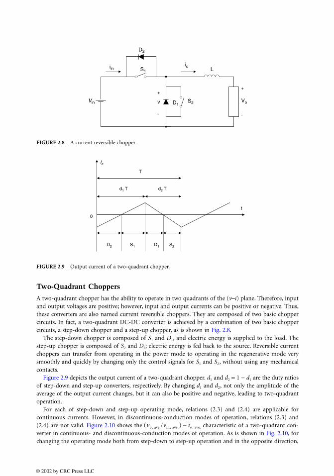
Two-Quadrant Choppers
A two-quadrant chopper has the ability to operate in two quadrants of the (v–i) plane. Therefore, inputand output voltages are positive; however, input and output currents can be positive or negative. Thus,these converters are also named current reversible choppers. They are composed of two basic choppercircuits. In fact, a two-quadrant DC-DC converter is achieved by a combination of two basic choppercircuits, a step-down chopper and a step-up chopper, as is shown in Fig. 2.8.
The step-down chopper is composed of S1 and D1, and electric energy is supplied to the load. Thestep-up chopper is composed of S2 and D2; electric energy is fed back to the source. Reversible currentchoppers can transfer from operating in the power mode to operating in the regenerative mode verysmoothly and quickly by changing only the control signals for S1 and S2, without using any mechanicalcontacts.
Figure 2.9 depicts the output current of a two-quadrant chopper. d1 and d2 = 1 − d1 are the duty ratiosof step-down and step-up converters, respectively. By changing d1 and d2, not only the amplitude of theaverage of the output current changes, but it can also be positive and negative, leading to two-quadrantoperation.
For each of step-down and step-up operating mode, relations (2.3) and (2.4) are applicable forcontinuous currents. However, in discontinuous-conduction modes of operation, relations (2.3) and(2.4) are not valid. Figure 2.10 shows the characteristic of a two-quadrant con-verter in continuous- and discontinuous-conduction modes of operation. As is shown in Fig. 2.10, forchanging the operating mode both from step-down to step-up operation and in the opposite direction,
FIGURE 2.8 A current reversible chopper.
FIGURE 2.9 Output current of a two-quadrant chopper.
+
-
io
D1
S1iin
v
+
-
L
S2
D2
VoVin
t
T
0
D2 D1 S2S1
io
d1 T d2 T
(vo , ave./vin, ave.) io , ave.–
© 2002 by CRC Press LLC
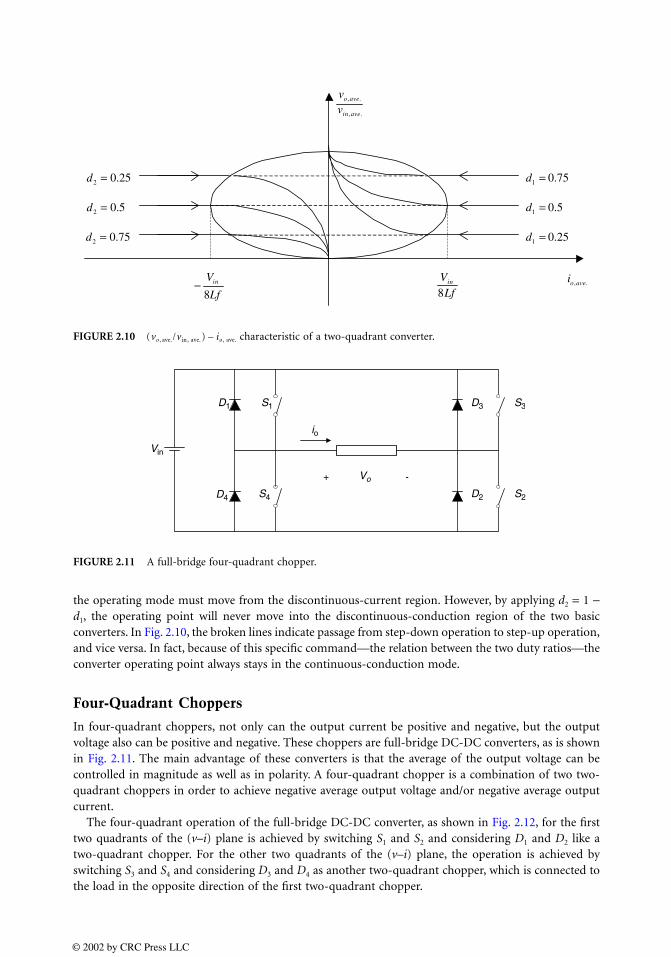
the operating mode must move from the discontinuous-current region. However, by applying d2 = 1 −d1, the operating point will never move into the discontinuous-conduction region of the two basicconverters. In Fig. 2.10, the broken lines indicate passage from step-down operation to step-up operation,and vice versa. In fact, because of this specific command—the relation between the two duty ratios—theconverter operating point always stays in the continuous-conduction mode.
Four-Quadrant Choppers
In four-quadrant choppers, not only can the output current be positive and negative, but the outputvoltage also can be positive and negative. These choppers are full-bridge DC-DC converters, as is shownin Fig. 2.11. The main advantage of these converters is that the average of the output voltage can becontrolled in magnitude as well as in polarity. A four-quadrant chopper is a combination of two two-quadrant choppers in order to achieve negative average output voltage and/or negative average outputcurrent.
The four-quadrant operation of the full-bridge DC-DC converter, as shown in Fig. 2.12, for the firsttwo quadrants of the (v–i) plane is achieved by switching S1 and S2 and considering D1 and D2 like atwo-quadrant chopper. For the other two quadrants of the (v–i) plane, the operation is achieved byswitching S3 and S4 and considering D3 and D4 as another two-quadrant chopper, which is connected tothe load in the opposite direction of the first two-quadrant chopper.
FIGURE 2.10 characteristic of a two-quadrant converter.
FIGURE 2.11 A full-bridge four-quadrant chopper.
.,aveinv.,aveov
.,aveoiVin
Lf8Lf
Vin
8−
5.01 =d
25.01 =d
75.01 =d
75.02 =d
5.02 =d
25.02 =d
(vo , ave./vin, ave.) io , ave.–
+ -
D1 S1
S2D2D4
D3
S4
S3
Vin
Vo
io
© 2002 by CRC Press LLC

2.3 Buck Converters
Richard Wies, Bipin Satavalekar, and Ashish Agrawal
The buck or step-down converter regulates the average DC output voltage at a level lower than the inputor source voltage. This is accomplished through controlled switching where the DC input voltage isturned on and off periodically, resulting in a lower average output voltage [1]. The buck converter iscommonly used in regulated DC power supplies like those in computers and instrumentation [1, 2].The buck converter is also used to provide a variable DC voltage to the armature of a DC motor forvariable speed drive applications [2].
Ideal Buck Circuit
The circuit that models the basic operation of the buck converter with an ideal switch and a purelyresistive load is shown in Fig. 2.13. The output voltage equals the input voltage when the switch is inposition 1 and the output voltage is zero when the switch is in position 2. The resulting output voltageis a rectangular voltage waveform with an average value as shown in Fig. 2.2 (in Section 2.1). The averageoutput voltage level is varied by adjusting the time the switch is in position 1 and 2 or the duty ratio.The resulting average output voltage Vo is given in terms of the duty ratio and the input voltage Vi byEq. (2.5) [2].
Vo = DVi (2.5)
The square wave output voltage for the ideal circuit of the buck converter contains an undesirableamount of voltage ripple. The circuit is modified by adding an inductor L in series and a capacitor C inparallel with the load resistor as shown in Fig. 2.14. The inductor reduces the ripple in the current through
FIGURE 2.12 Four-quadrant operation of a full-bridge chopper.
FIGURE 2.13 Ideal buck converter.
., aveov
., aveoi
>
>
0
0
.,
.,
aveo
aveo
i
v
<
>
0
0
.,
.,
aveo
aveo
i
v
<
<
0
0
.,
.,
aveo
aveo
i
v
>
<
0
0
.,
.,
aveo
aveo
i
v
S
++
1
2
R VoVi
© 2002 by CRC Press LLC
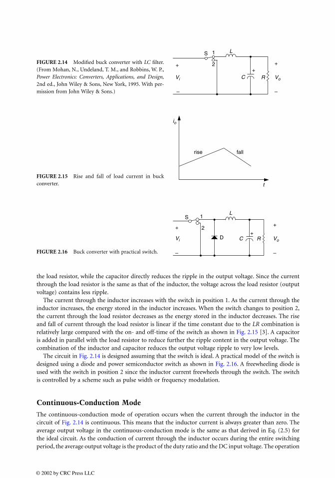
the load resistor, while the capacitor directly reduces the ripple in the output voltage. Since the currentthrough the load resistor is the same as that of the inductor, the voltage across the load resistor (outputvoltage) contains less ripple.
The current through the inductor increases with the switch in position 1. As the current through theinductor increases, the energy stored in the inductor increases. When the switch changes to position 2,the current through the load resistor decreases as the energy stored in the inductor decreases. The riseand fall of current through the load resistor is linear if the time constant due to the LR combination isrelatively large compared with the on- and off-time of the switch as shown in Fig. 2.15 [3]. A capacitoris added in parallel with the load resistor to reduce further the ripple content in the output voltage. Thecombination of the inductor and capacitor reduces the output voltage ripple to very low levels.
The circuit in Fig. 2.14 is designed assuming that the switch is ideal. A practical model of the switch isdesigned using a diode and power semiconductor switch as shown in Fig. 2.16. A freewheeling diode isused with the switch in position 2 since the inductor current freewheels through the switch. The switchis controlled by a scheme such as pulse width or frequency modulation.
Continuous-Conduction Mode
The continuous-conduction mode of operation occurs when the current through the inductor in thecircuit of Fig. 2.14 is continuous. This means that the inductor current is always greater than zero. Theaverage output voltage in the continuous-conduction mode is the same as that derived in Eq. (2.5) forthe ideal circuit. As the conduction of current through the inductor occurs during the entire switchingperiod, the average output voltage is the product of the duty ratio and the DC input voltage. The operation
FIGURE 2.14 Modified buck converter with LC filter.(From Mohan, N., Undeland, T. M., and Robbins, W. P.,Power Electronics: Converters, Applications, and Design,2nd ed., John Wiley & Sons, New York, 1995. With per-mission from John Wiley & Sons.)
FIGURE 2.15 Rise and fall of load current in buckconverter.
FIGURE 2.16 Buck converter with practical switch.
Vi
2
1
+ ++
C
L
R Vo
S
io
t
fallrise
2
1
+ +
D
S
+C
L
R VoVi
© 2002 by CRC Press LLC
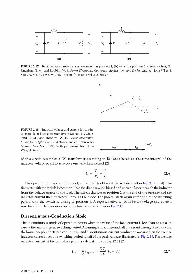
of this circuit resembles a DC transformer according to Eq. (2.6) based on the time-integral of theinductor voltage equal to zero over one switching period [2].
(2.6)
The operation of the circuit in steady state consists of two states as illustrated in Fig. 2.17 [2, 4]. Thefirst state with the switch in position 1 has the diode reverse-biased and current flows through the inductorfrom the voltage source to the load. The switch changes to position 2 at the end of the on-time and theinductor current then freewheels through the diode. The process starts again at the end of the switchingperiod with the switch returning to position 1. A representative set of inductor voltage and currentwaveforms for the continuous-conduction mode is shown in Fig. 2.18.
Discontinuous-Conduction Mode
The discontinuous mode of operation occurs when the value of the load current is less than or equal tozero at the end of a given switching period. Assuming a linear rise and fall of current through the inductor,the boundary point between continuous- and discontinuous-current conduction occurs when the averageinductor current over one switching period is half of the peak value, as illustrated in Fig. 2.19. The averageinductor current at the boundary point is calculated using Eq. (2.7) [2].
(2.7)
FIGURE 2.17 Buck converter switch states: (a) switch in position 1; (b) switch in position 2. (From Mohan, N.,Undeland, T. M., and Robbins, W. P., Power Electronics: Converters, Applications, and Design, 2nd ed., John Wiley &Sons, New York, 1995. With permission from John Wiley & Sons.)
FIGURE 2.18 Inductor voltage and current for contin-uous mode of buck converter. (From Mohan, N., Unde-land, T. M., and Robbins, W. P., Power Electronics:Converters, Applications, and Design, 2nd ed., John Wiley& Sons, New York, 1995. With permission from JohnWiley & Sons.)
vL
IL
ton toffVo
iL
Vi Vo
t
DVo
Vi
-----Ii
Io
---= =
ILB12-- iL peak( )
DTs
2L--------- Vi Vo–( )= =
(a) (b)
D
++
Vi Vo
+C
L
R
+
VoD
+
Vi
+C
L
R
© 2002 by CRC Press LLC
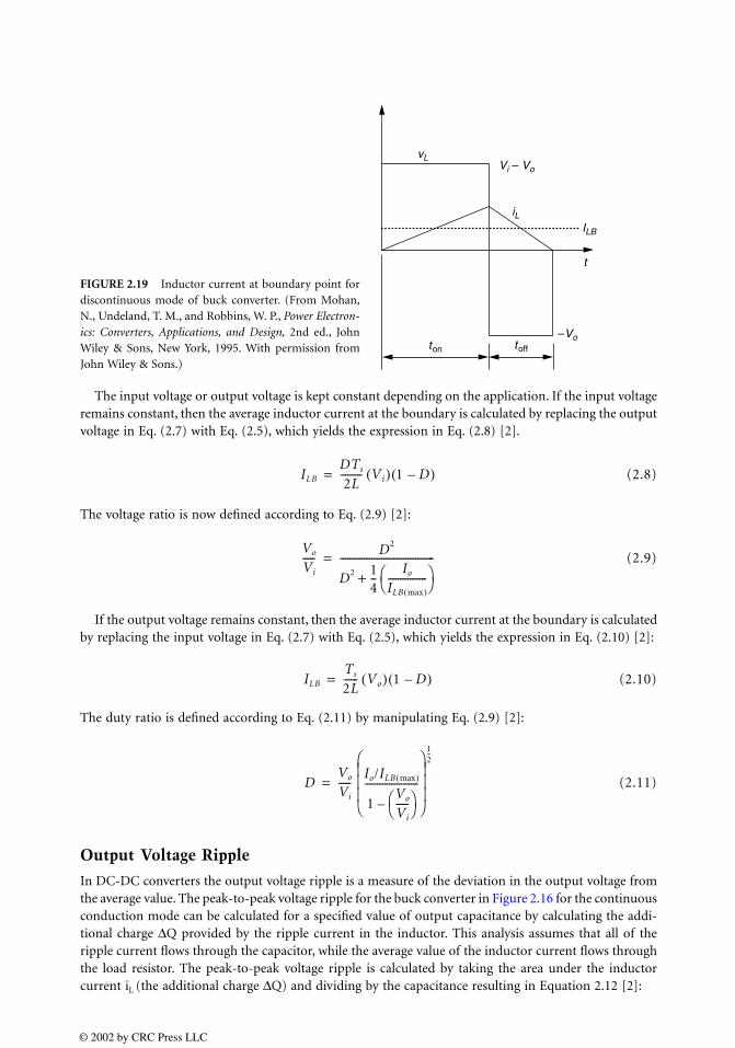
The input voltage or output voltage is kept constant depending on the application. If the input voltageremains constant, then the average inductor current at the boundary is calculated by replacing the outputvoltage in Eq. (2.7) with Eq. (2.5), which yields the expression in Eq. (2.8) [2].
(2.8)
The voltage ratio is now defined according to Eq. (2.9) [2]:
(2.9)
If the output voltage remains constant, then the average inductor current at the boundary is calculatedby replacing the input voltage in Eq. (2.7) with Eq. (2.5), which yields the expression in Eq. (2.10) [2]:
(2.10)
The duty ratio is defined according to Eq. (2.11) by manipulating Eq. (2.9) [2]:
(2.11)
Output Voltage Ripple
In DC-DC converters the output voltage ripple is a measure of the deviation in the output voltage fromthe average value. The peak-to-peak voltage ripple for the buck converter in Figure 2.16 for the continuousconduction mode can be calculated for a specified value of output capacitance by calculating the addi-tional charge ∆Q provided by the ripple current in the inductor. This analysis assumes that all of theripple current flows through the capacitor, while the average value of the inductor current flows throughthe load resistor. The peak-to-peak voltage ripple is calculated by taking the area under the inductorcurrent iL (the additional charge ∆Q) and dividing by the capacitance resulting in Equation 2.12 [2]:
FIGURE 2.19 Inductor current at boundary point fordiscontinuous mode of buck converter. (From Mohan,N., Undeland, T. M., and Robbins, W. P., Power Electron-ics: Converters, Applications, and Design, 2nd ed., JohnWiley & Sons, New York, 1995. With permission fromJohn Wiley & Sons.)
ton toff
t
vL
ILB
Vo
iL
Vi Vo
ILB
DTs
2L--------- Vi( ) 1 D–( )=
Vo
Vi
----- D2
D2 14--
Io
ILB max( )----------------
+---------------------------------------=
ILB
Ts
2L------ Vo( ) 1 D–( )=
DVo
Vi
-----Io/ILB max( )
1Vo
Vi
----- –
----------------------
12--
=
© 2002 by CRC Press LLC
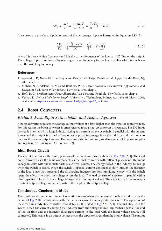
(2.12)
It is customary to refer to ripple in terms of the percentage ripple as illustrated in Equation 2.13 [2]:
(2.13)
where fs is the switching frequency and fc is the corner frequency of the low-pass LC filter on the output.The voltage ripple is minimized by selecting a corner frequency for the lowpass filter which is much lessthan the switching frequency.
References
1. Agrawal, J. P., Power Electronics Systems: Theory and Design, Prentice-Hall, Upper Saddle River, NJ,2001, chap. 6.
2. Mohan, N., Undeland, T. M., and Robbins, W. P., Power Electronics: Converters, Applications, andDesign, 2nd ed., John Wiley & Sons, New York, 1995, chap. 7.
3. Hoft, R. G., Semiconductor Power Electronics, Van Nostrand Reinhold, New York, 1986, chap. 5.4. Venkat, R., Switch Mode Power Supply, University of Technology, Sydney, Australia, 01 March 2001,
available at http://www.ee.uts.edu.au/~venkat/pe_html/pe07_nc8.htm.
2.4 Boost Converters
Richard Wies, Bipin Satavalekar, and Ashish Agrawal
A boost converter regulates the average output voltage at a level higher than the input or source voltage.For this reason the boost converter is often referred to as a step-up converter or regulator. The DC inputvoltage is in series with a large inductor acting as a current source. A switch in parallel with the currentsource and the output is turned off periodically, providing energy from the inductor and the source toincrease the average output voltage. The boost converter is commonly used in regulated DC power suppliesand regenerative braking of DC motors [1, 2].
Ideal Boost Circuit
The circuit that models the basic operation of the boost converter is shown in Fig. 2.20 [2, 3]. The idealboost converter uses the same components as the buck converter with different placement. The inputvoltage in series with the inductor acts as a current source. The energy stored in the inductor builds upwhen the switch is closed. When the switch is opened, current continues to flow through the inductorto the load. Since the source and the discharging inductor are both providing energy with the switchopen, the effect is to boost the voltage across the load. The load consists of a resistor in parallel with afilter capacitor. The capacitor voltage is larger than the input voltage. The capacitor is large to keep aconstant output voltage and acts to reduce the ripple in the output voltage.
Continuous-Conduction Mode
The continuous-conduction mode of operation occurs when the current through the inductor in thecircuit of Fig. 2.20 is continuous with the inductor current always greater than zero. The operation ofthe circuit in steady state consists of two states, as illustrated in Fig. 2.21 [2, 3]. The first state with theswitch closed has current charging the inductor from the voltage source. The switch opens at the endof the on-time and the inductor discharges current to the load with the input voltage source stillconnected. This results in an output voltage across the capacitor larger than the input voltage. The output
∆Vo∆QC
--------1C---1
2--
∆IL
2--------
Ts
2-----
Ts
8C-------
Vo
L----- 1 D–( )Ts= = =
∆Vo
Vo
---------18--
Ts2 1 D–( )
LC------------------------ π2
2----- 1 D–( )
fc
fs
---
2
= =
© 2002 by CRC Press LLC

voltage remains constant if the RC time constant is significantly larger than the on-time of the switch.A representative set of inductor voltage and current waveforms for the continuous conduction mode isshown in Fig. 2.22 [2].
The voltage ratio for a boost converter is derived based on the time-integral of the inductor voltageequal to zero over one switching period. The voltage ratio is equivalent to the ratio of the switchingperiod to the off-time of the switch as illustrated by Eq. (2.14) [2].
(2.14)
The current ratio is derived from the voltage ratio assuming that the input power is equal to the outputpower, as with ideal transformer analysis.
FIGURE 2.20 Basic boost converter. (From Mohan, N.,Undeland, T. M., and Robbins, W. P., Power Electronics:Converters, Applications, and Design, 2nd ed., John Wiley& Sons, New York, 1995. With permission from JohnWiley & Sons.)
FIGURE 2.21 Basic boost converter switch states: (a) switch closed; (b) switch open. (From Mohan, N., Undeland,T. M., and Robbins, W. P., Power Electronics: Converters, Applications, and Design, 2nd ed., John Wiley & Sons, NewYork, 1995. With permission from John Wiley & Sons.)
FIGURE 2.22 Inductor voltage and current waveformsfor continuous mode of boost converter. (From Mohan,N., Undeland, T. M., and Robbins, W. P., Power Electron-ics: Converters, Applications, and Design, 2nd ed., JohnWiley & Sons, New York, 1995. With permission fromJohn Wiley & Sons.)
Vi
++
D
S+
C
L
R Vo
D
+ +
Vi Vo Vi Vo
+
C
L
R
(a)
D
+ ++
C R
(b)
L
Vi Vo
ILiL
vLVi
toffton
t
Vo
Vi
-----Ii
Io
---Ts
toff
------Ts
Ts toff–----------------- T
1 D–-------------= = = =
© 2002 by CRC Press LLC

Discontinuous-Conduction Mode
The discontinuous mode of operation occurs when the value of the load current is less than or equal tozero at the end of a given switching period. Assuming a linear rise and fall of current through the inductor,the boundary point between continuous- and discontinuous-current conduction occurs when the averageinductor current over one switching period is half the peak value, as illustrated in Fig. 2.23 [2]. The averageinductor current at the boundary point is calculated using Eq. (2.15) [2].
(2.15)
The output current at the boundary condition is derived by using the current ratio of Eq. (2.14) in Eq. (2.15)with the inductor current equal to the input current. This results in Eq. (2.16) [2]:
(2.16)
For the boost converter in discontinuous mode, the output voltage Vo is generally kept constant whilethe duty ratio D varies in response to changes in the input voltage Vi.
The duty ratio is defined as a function of the output current for various values of the voltage ratioaccording to Eq. (2.17) [2]:
(2.17)
Output Voltage Ripple
The peak-to-peak voltage ripple for the boost converter in Figure 2.20 for the continuous conductionmode can be calculated for a specified value of output capacitance by calculating the additional charge∆Q provided by the ripple current in the inductor. This analysis is similar to that discussed for the buckconverter. The peak-to-peak voltage ripple is calculated by taking the area under the inductor current iL
(the additional charge ∆Q) and dividing by the capacitance resulting in Equation 2.18 [2]:
FIGURE 2.23 Inductor current at boundary point fordiscontinuous mode of boost converter. (From Mohan,N., Undeland, T. M., and Robbins, W. P., Power Electron-ics: Converters, Applications, and Design, 2nd ed., JohnWiley & Sons, New York, 1995. With permission fromJohn Wiley & Sons.)
ILB
iL
vL
toff
t
ton
ILB12-- iL peak( )
VoTs
2L----------- D 1 D–( )= =
IOB
VoTs
2L----------- D 1 D–( )2=
D4
27-----
Vo
Vi
-----Vo
Vi
----- 1– Io
IoB max( )----------------=
12--
© 2002 by CRC Press LLC
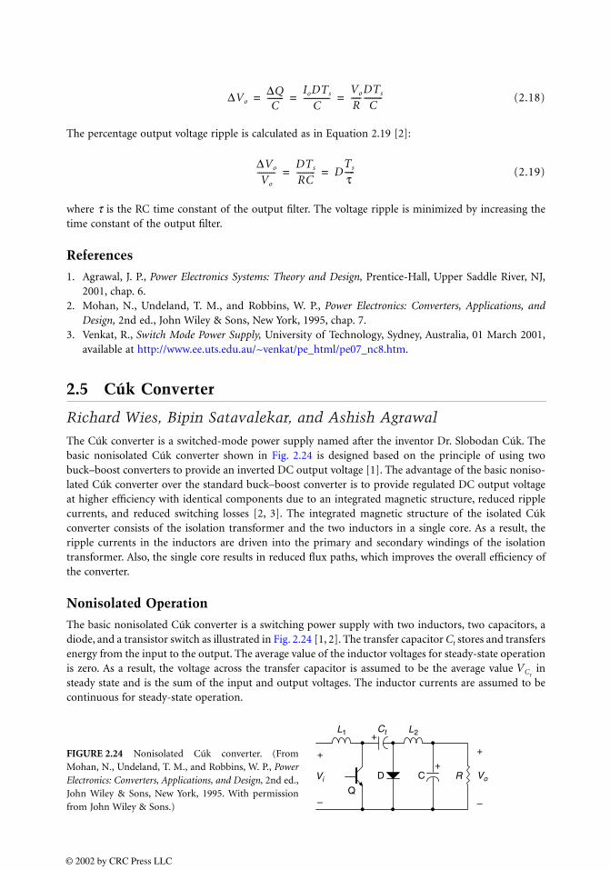
(2.18)
The percentage output voltage ripple is calculated as in Equation 2.19 [2]:
(2.19)
where τ is the RC time constant of the output filter. The voltage ripple is minimized by increasing thetime constant of the output filter.
References
1. Agrawal, J. P., Power Electronics Systems: Theory and Design, Prentice-Hall, Upper Saddle River, NJ,2001, chap. 6.
2. Mohan, N., Undeland, T. M., and Robbins, W. P., Power Electronics: Converters, Applications, andDesign, 2nd ed., John Wiley & Sons, New York, 1995, chap. 7.
3. Venkat, R., Switch Mode Power Supply, University of Technology, Sydney, Australia, 01 March 2001,available at http://www.ee.uts.edu.au/~venkat/pe_html/pe07_nc8.htm.
2.5 Cúk Converter
Richard Wies, Bipin Satavalekar, and Ashish Agrawal
The Cúk converter is a switched-mode power supply named after the inventor Dr. Slobodan Cúk. Thebasic nonisolated Cúk converter shown in Fig. 2.24 is designed based on the principle of using twobuck–boost converters to provide an inverted DC output voltage [1]. The advantage of the basic noniso-lated Cúk converter over the standard buck–boost converter is to provide regulated DC output voltageat higher efficiency with identical components due to an integrated magnetic structure, reduced ripplecurrents, and reduced switching losses [2, 3]. The integrated magnetic structure of the isolated Cúkconverter consists of the isolation transformer and the two inductors in a single core. As a result, theripple currents in the inductors are driven into the primary and secondary windings of the isolationtransformer. Also, the single core results in reduced flux paths, which improves the overall efficiency ofthe converter.
Nonisolated Operation
The basic nonisolated Cúk converter is a switching power supply with two inductors, two capacitors, adiode, and a transistor switch as illustrated in Fig. 2.24 [1, 2]. The transfer capacitor Ct stores and transfersenergy from the input to the output. The average value of the inductor voltages for steady-state operationis zero. As a result, the voltage across the transfer capacitor is assumed to be the average value insteady state and is the sum of the input and output voltages. The inductor currents are assumed to becontinuous for steady-state operation.
FIGURE 2.24 Nonisolated Cúk converter. (FromMohan, N., Undeland, T. M., and Robbins, W. P., PowerElectronics: Converters, Applications, and Design, 2nd ed.,John Wiley & Sons, New York, 1995. With permissionfrom John Wiley & Sons.)
∆Vo∆QC
--------IoDTs
C-------------
Vo
R-----
DTs
C---------= = =
∆Vo
Vo
---------DTs
RC--------- D
Ts
τ-----= =
VCt
+ +
Q
D VoVi
+C
+Ct
R
L1 L2
© 2002 by CRC Press LLC
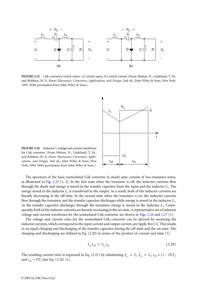
The operation of the basic nonisolated Cúk converter in steady state consists of two transistor states,as illustrated in Fig. 2.25 [1, 2]. In the first state when the transistor is off, the inductor currents flowthrough the diode and energy is stored in the transfer capacitor from the input and the inductor L1. Theenergy stored in the inductor L2 is transferred to the output. As a result, both of the inductor currents arelinearly decreasing in the off-state. In the second state when the transistor is on, the inductor currentsflow through the transistor and the transfer capacitor discharges while energy is stored in the inductor L1.As the transfer capacitor discharges through the transistor, energy is stored in the inductor L2. Conse-quently, both of the inductor currents are linearly increasing in the on-state. A representative set of inductorvoltage and current waveforms for the nonisolated Cúk converter are shown in Figs. 2.26 and 2.27 [1].
The voltage and current ratio for the nonisolated Cúk converter can be derived by assuming theinductor currents, which correspond to the input current and output current, are ripple-free [1]. This resultsin an equal charging and discharging of the transfer capacitor during the off-state and the on-state. Thecharging and discharging are defined in Eq. (2.20) in terms of the product of current and time [1].
(2.20)
The resulting current ratio is expressed in Eq. (2.21) by substituting toff = (1 − D)Ts,and ton = DTs into Eq. (2.20) [1].
FIGURE 2.25 Cúk converter switch states: (a) switch open; (b) switch closed. (From Mohan, N., Undeland, T. M.,and Robbins, W. P., Power Electronics: Converters, Applications, and Design, 2nd ed., John Wiley & Sons, New York,1995. With permission from John Wiley & Sons.)
FIGURE 2.26 Inductor 1, voltage and current waveformsfor Cúk converter. (From Mohan, N., Undeland, T. M.,and Robbins, W. P., Power Electronics: Converters, Appli-cations, and Design, 2nd ed., John Wiley & Sons, NewYork, 1995. With permission from John Wiley & Sons.)
(a) (b)
+ VCtVCt
+
+ +
D VoVi
+C
+Ct
R
L1 L2
+ +
D VoVi
+C
+Ct
R
L1 L2
toff ton
t
Vo
ViiL1
VL1
IL1toff IL2
ton=
IL1Ii, IL2
Io,= =
© 2002 by CRC Press LLC
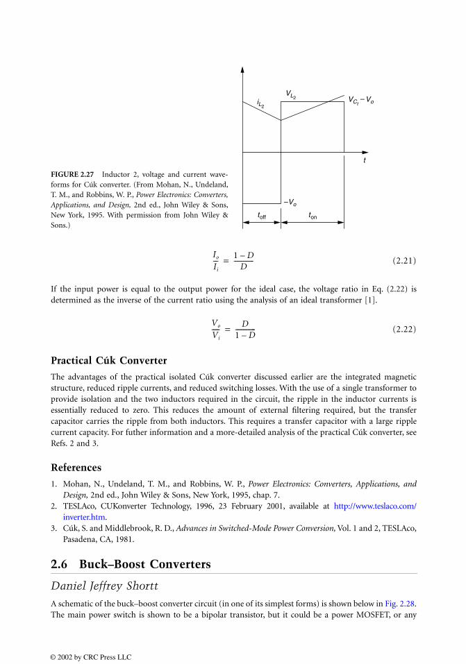
(2.21)
If the input power is equal to the output power for the ideal case, the voltage ratio in Eq. (2.22) isdetermined as the inverse of the current ratio using the analysis of an ideal transformer [1].
(2.22)
Practical Cúk Converter
The advantages of the practical isolated Cúk converter discussed earlier are the integrated magneticstructure, reduced ripple currents, and reduced switching losses. With the use of a single transformer toprovide isolation and the two inductors required in the circuit, the ripple in the inductor currents isessentially reduced to zero. This reduces the amount of external filtering required, but the transfercapacitor carries the ripple from both inductors. This requires a transfer capacitor with a large ripplecurrent capacity. For futher information and a more-detailed analysis of the practical Cúk converter, seeRefs. 2 and 3.
References
1. Mohan, N., Undeland, T. M., and Robbins, W. P., Power Electronics: Converters, Applications, andDesign, 2nd ed., John Wiley & Sons, New York, 1995, chap. 7.
2. TESLAco, CUKonverter Technology, 1996, 23 February 2001, available at http://www.teslaco.com/inverter.htm.
3. Cúk, S. and Middlebrook, R. D., Advances in Switched-Mode Power Conversion, Vol. 1 and 2, TESLAco,Pasadena, CA, 1981.
2.6 Buck–Boost Converters
Daniel Jeffrey Shortt
A schematic of the buck–boost converter circuit (in one of its simplest forms) is shown below in Fig. 2.28.The main power switch is shown to be a bipolar transistor, but it could be a power MOSFET, or any
FIGURE 2.27 Inductor 2, voltage and current wave-forms for Cúk converter. (From Mohan, N., Undeland,T. M., and Robbins, W. P., Power Electronics: Converters,Applications, and Design, 2nd ed., John Wiley & Sons,New York, 1995. With permission from John Wiley &Sons.)
VL2 VCtVo
Vo
iL2
toff ton
t
Io
Ii
--- 1 D–D
-------------=
Vo
Vi
----- D1 D–-------------=
© 2002 by CRC Press LLC
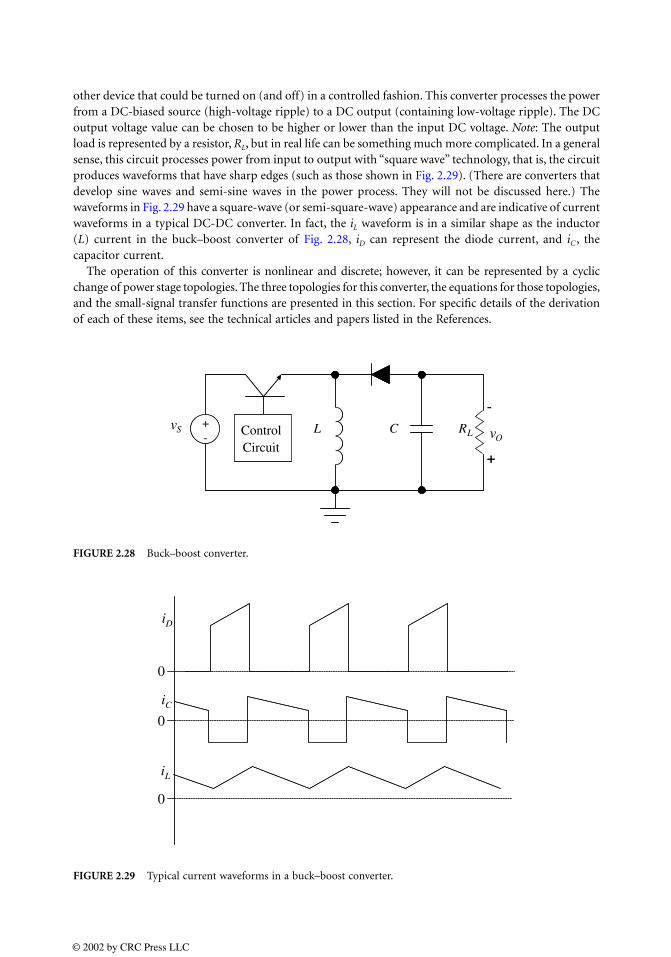
other device that could be turned on (and off) in a controlled fashion. This converter processes the powerfrom a DC-biased source (high-voltage ripple) to a DC output (containing low-voltage ripple). The DCoutput voltage value can be chosen to be higher or lower than the input DC voltage. Note: The outputload is represented by a resistor, RL, but in real life can be something much more complicated. In a generalsense, this circuit processes power from input to output with “square wave” technology, that is, the circuitproduces waveforms that have sharp edges (such as those shown in Fig. 2.29). (There are converters thatdevelop sine waves and semi-sine waves in the power process. They will not be discussed here.) Thewaveforms in Fig. 2.29 have a square-wave (or semi-square-wave) appearance and are indicative of currentwaveforms in a typical DC-DC converter. In fact, the iL waveform is in a similar shape as the inductor(L) current in the buck–boost converter of Fig. 2.28, iD can represent the diode current, and iC , thecapacitor current.
The operation of this converter is nonlinear and discrete; however, it can be represented by a cyclicchange of power stage topologies. The three topologies for this converter, the equations for those topologies,and the small-signal transfer functions are presented in this section. For specific details of the derivationof each of these items, see the technical articles and papers listed in the References.
FIGURE 2.28 Buck–boost converter.
FIGURE 2.29 Typical current waveforms in a buck–boost converter.
+-
-
+
RCLControlCircuit
vS+-
-
+
vOLControlCircuit
0
0
0
i
iL
iC
D
© 2002 by CRC Press LLC
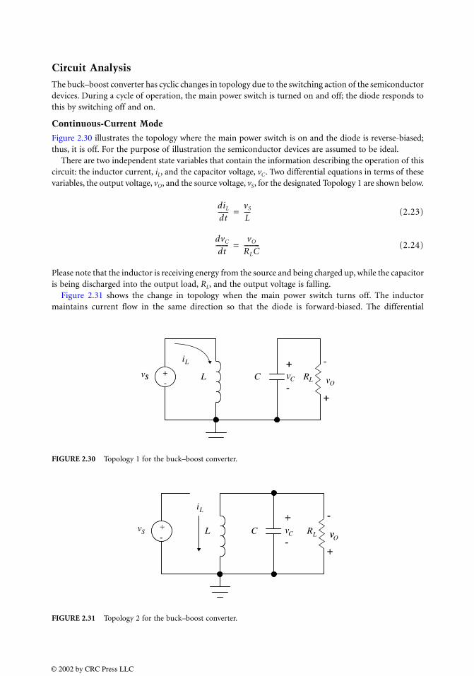
Circuit Analysis
The buck–boost converter has cyclic changes in topology due to the switching action of the semiconductordevices. During a cycle of operation, the main power switch is turned on and off; the diode responds tothis by switching off and on.
Continuous-Current Mode
Figure 2.30 illustrates the topology where the main power switch is on and the diode is reverse-biased;thus, it is off. For the purpose of illustration the semiconductor devices are assumed to be ideal.
There are two independent state variables that contain the information describing the operation of thiscircuit: the inductor current, iL, and the capacitor voltage, vC. Two differential equations in terms of thesevariables, the output voltage, vO, and the source voltage, vS, for the designated Topology 1 are shown below.
(2.23)
(2.24)
Please note that the inductor is receiving energy from the source and being charged up, while the capacitoris being discharged into the output load, RL, and the output voltage is falling.
Figure 2.31 shows the change in topology when the main power switch turns off. The inductormaintains current flow in the same direction so that the diode is forward-biased. The differential
FIGURE 2.30 Topology 1 for the buck–boost converter.
FIGURE 2.31 Topology 2 for the buck–boost converter.
diL
dt-------
vS
L----=
dvC
dt--------
vO
RLC----------=
vS+-
-
+
vORCL
i +
-S
+-
-
+
L
L +vC
-
vS+-
-
+
vORLCL
iL+vC
-
+-
-
+
v
+
-
© 2002 by CRC Press LLC
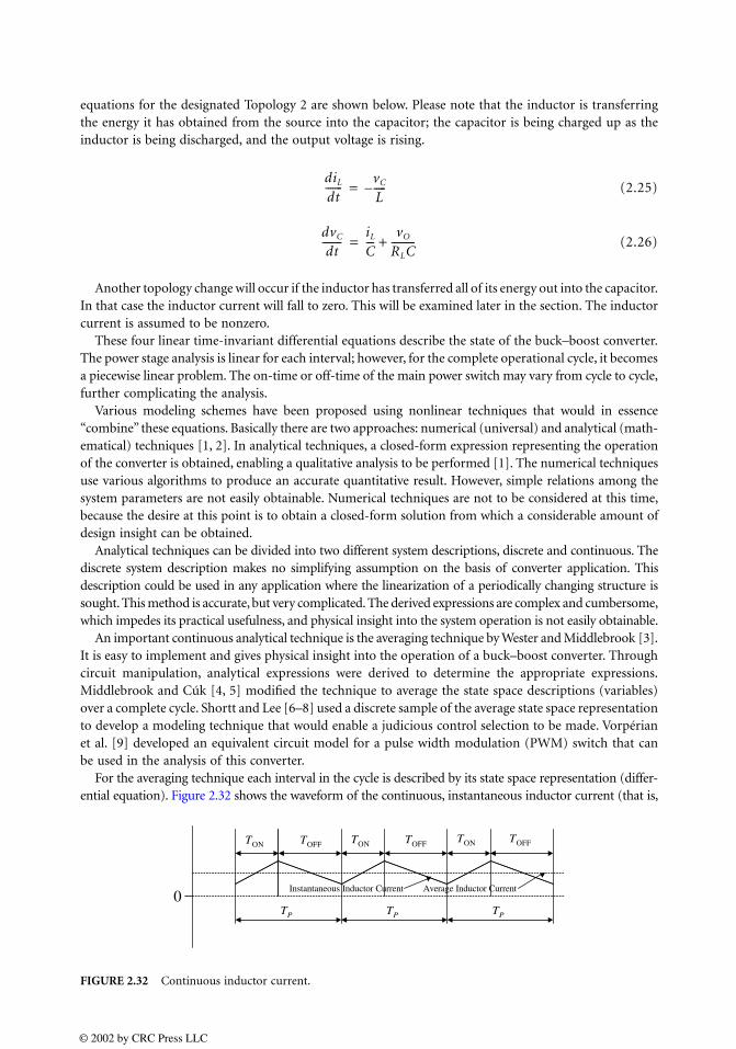
equations for the designated Topology 2 are shown below. Please note that the inductor is transferringthe energy it has obtained from the source into the capacitor; the capacitor is being charged up as theinductor is being discharged, and the output voltage is rising.
(2.25)
(2.26)
Another topology change will occur if the inductor has transferred all of its energy out into the capacitor.In that case the inductor current will fall to zero. This will be examined later in the section. The inductorcurrent is assumed to be nonzero.
These four linear time-invariant differential equations describe the state of the buck–boost converter.The power stage analysis is linear for each interval; however, for the complete operational cycle, it becomesa piecewise linear problem. The on-time or off-time of the main power switch may vary from cycle to cycle,further complicating the analysis.
Various modeling schemes have been proposed using nonlinear techniques that would in essence“combine” these equations. Basically there are two approaches: numerical (universal) and analytical (math-ematical) techniques [1, 2]. In analytical techniques, a closed-form expression representing the operationof the converter is obtained, enabling a qualitative analysis to be performed [1]. The numerical techniquesuse various algorithms to produce an accurate quantitative result. However, simple relations among thesystem parameters are not easily obtainable. Numerical techniques are not to be considered at this time,because the desire at this point is to obtain a closed-form solution from which a considerable amount ofdesign insight can be obtained.
Analytical techniques can be divided into two different system descriptions, discrete and continuous. Thediscrete system description makes no simplifying assumption on the basis of converter application. Thisdescription could be used in any application where the linearization of a periodically changing structure issought. This method is accurate, but very complicated. The derived expressions are complex and cumbersome,which impedes its practical usefulness, and physical insight into the system operation is not easily obtainable.
An important continuous analytical technique is the averaging technique by Wester and Middlebrook [3].It is easy to implement and gives physical insight into the operation of a buck–boost converter. Throughcircuit manipulation, analytical expressions were derived to determine the appropriate expressions.Middlebrook and Cúk [4, 5] modified the technique to average the state space descriptions (variables)over a complete cycle. Shortt and Lee [6–8] used a discrete sample of the average state space representationto develop a modeling technique that would enable a judicious control selection to be made. Vorpérianet al. [9] developed an equivalent circuit model for a pulse width modulation (PWM) switch that canbe used in the analysis of this converter.
For the averaging technique each interval in the cycle is described by its state space representation (differ-ential equation). Figure 2.32 shows the waveform of the continuous, instantaneous inductor current (that is,
FIGURE 2.32 Continuous inductor current.
diL
dt-------
vC
L-----–=
dvC
dt--------
iL
C---
vO
RLC----------+=
0
TON TOFF TOFFTOFFTON
TON
TP TP TP
Instantaneous Inductor Current Average Inductor Current
© 2002 by CRC Press LLC

iL does not equal zero at any point in time) and the average inductor current for the buck–boost converter(Fig. 2.30). The instantaneous current is cyclic with a time period equal to TP s; the main power switchis on for TON s and off for TOFF s. The equations are averaged to give a single period representation, asshown below:
(2.27)
(2.28)
where iL and vC are average state variables, d = TON/TP and d ′ = TOFF/TP. Please note: To study the small signal behavior, the time-varying system described in Eqs. (2.27) and (2.28) can
be linearized using small signal perturbation techniques. By using these techniques, the inputs areassumed to vary around a steady-state operating point. Taking a first-order Fourier series approximation,the inputs are represented by the sum of a DC or steady-state term and an AC variation or sinusoidalterm. Introducing variations in the line voltage and duty cycle by the following substitutions
cause perturbations in the state and output, as shown below. In the above and following equations thevariables in capital letters represent the DC or steady-state term; and the variables with the symbol “ ”above them represent the AC variation or sinusoidal term.
Figure 2.33 shows the type of change that is being modeled for an inductor current perturbation ofFig. 2.32. Note the TON and TOFF slowly change from cycle to cycle, which produces a slight change inthe inductor current from cycle to cycle.
The derivative of a DC term is zero, so the above equations can be simplified to the following:
Substituting these equations into (2.27) and (2.28), separating the DC (steady-state) terms and the AC(sinusoidal) terms results in the following:
FIGURE 2.33 Inductor current perturbation.
iL d– ′vC
L----- d
vS
L----+=
vC d′iL
C---
vO
RLC----------+=
d d′+ 1.=
vS VS v s, d+ D d , d′+ D′ d–= = =
ˆ
iL IL iLˆ , iL+ IL i L, vC
˙+ VC vCˆ , vC+ VC v c, vO+ VO vO+= = = = =
iL iL˙
, iL IL iL, vC+ vCˆ , vC VC vc, vO+ VO vO+= = = = =
0
TON TOFF TOFF TOFFTON TON
TP TP TP
Instantaneous Inductor CurrentAverage Inductor Current
© 2002 by CRC Press LLC

DC terms:
(2.29)
(2.30)
AC terms (neglecting the higher-order terms):
(2.31)
(2.32)
The equation
is derived from Eq. (2.29). Note that from Fig. 2.28, vC = −vO , giving VC = −VO and substitutingthis into the previous equation results in:
(2.33)
Equation (2.33) states that the ratio of the DC output voltage to the DC input voltage is equal to theratio of the power switch on-time to the power switch off-time. The expression for the DC inductorcurrent term is
(2.34)
Equations (2.31) and (2.32) constitute the small signal model of a buck–boost converter.Another method that is utilized to extract the small signal model is to realize an equivalent circuit
model from Eqs. (2.27) and (2.28). Figure 2.34 is the average circuit model of the buck–boost converter.
FIGURE 2.34 Average circuit model of the buck–boost converter.
D′VC
L-------------
DVS
L----------+ 0=
D′IL
C----------
VO
RLC----------+ 0=
iL˙ D′vC
L----------- DvS
L---------
VS VC–L
------------------ d+ +=
vC
D′C------ iL
vO
RLC----------
IL
C---- d+ +=
VC
VS
------ DD′------–=
vC vO;–=
VO
VS
------ DD′------=
IL
VO
D′RL
------------–=
vS+-
-
+
RL
C
1:d
L
d:1
vC
iL+
-vO
© 2002 by CRC Press LLC
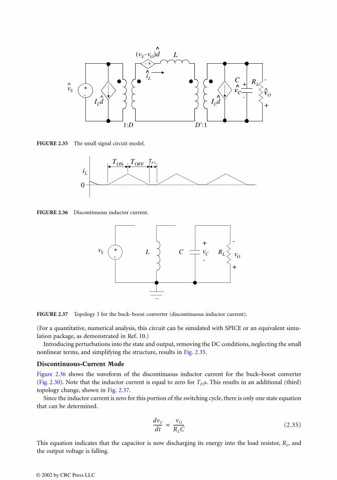
(For a quantitative, numerical analysis, this circuit can be simulated with SPICE or an equivalent simu-lation package, as demonstrated in Ref. 10.)
Introducing perturbations into the state and output, removing the DC conditions, neglecting the smallnonlinear terms, and simplifying the structure, results in Fig. 2.35.
Discontinuous-Current Mode
Figure 2.36 shows the waveform of the discontinuous inductor current for the buck–boost converter(Fig. 2.30). Note that the inductor current is equal to zero for TF2s. This results in an additional (third)topology change, shown in Fig. 2.37.
Since the inductor current is zero for this portion of the switching cycle, there is only one state equationthat can be determined.
(2.35)
This equation indicates that the capacitor is now discharging its energy into the load resistor, RL, andthe output voltage is falling.
FIGURE 2.35 The small signal circuit model.
FIGURE 2.36 Discontinuous inductor current.
FIGURE 2.37 Topology 3 for the buck–boost converter (discontinuous inductor current).
vOvS
+-
-
+
RLC
ILd
1:D
- +
(vS-vO)d^
L
D :1
^ILd
vC^
iL^
+
-v
+-
^
- +
^
^I
vC^
^
+
0
iL
TON TOFFTF2
vS+-
-
+
vORLCL
+vC
-
dvC
dt--------
vO
RLC----------=
© 2002 by CRC Press LLC

The modeling of this particular mode is presented in Refs. 5,11, and 12. A general discussion is providedhere as it applies to the model of the buck–boost converter in the discontinuous inductor current mode.
For this case, the inductor current does not behave as a true state variable, since diL/dt = 0, therebyreducing the system order by one. Figure 2.38 illustrates the general form of the inductor current. Theequations for the Ton time interval are the same as Eqs. (2.23) and (2.24), except iL = IR + , where IR
represents the DC level at which the inductor current begins and , the value of the time-varyinginductor current. The equations for the TOFF interval are the same as Eqs. (2.25) and (2.26) except iL =IR + , where represents the value of the time-varying inductor current. By combining these sets ofequations with Eq. (2.31) by the averaging technique, the equations listed below are obtained.
(2.36)
(2.37)
For the buck–boost converter case IR = 0; also, from Fig. 2.38, note that
(2.38)
The variable iAV is the average value of the inductor during the TON + TOFF time, not for the whole cycle.Substituting into Eqs. (2.36) and (2.37) results in the following:
(2.39)
Let
and substitute into the above equation.
(2.40)
FIGURE 2.38 General form of discontinuous inductor current.
IR
iL
TON TOFF TF2
iAV
iL∗
iL∗
iL∗∗ iL
∗∗
diL
dt------- 1
TP
-----vS
L---- td
1TP
-----vC–L
-------- td
TON
TON+TOFF
∫+0
TON
∫ 0= =
dvC
dt-------- 1
TP
-----vC
RLC----------–
td1
TP
-----IR iL
∗+C
--------------vC
RLC----------–
td1
TP
-----vC
RLC----------–
tdTON+TOFF
TON+TOFF+TF2
∫+TON
TON+TOFF
∫+0
TON
∫=
iL∗ td
TON
TON+TOFF
∫ 12--
vS
L---- TON
TOFF iAVTOFF= =
dvC
dt--------
TON
TP
---------–vC
RLC----------
TOFF
TP
----------iAV
C------
TOFF
TP
----------vC
RLC----------
TF2
TP
-------vC
RLC----------––+=
d1
TON
TP
--------- , d2
TOFF
TP
---------- , d3
TF2
TP
-------= = =
vC d2
iAV
C------
vC
RLC----------–=
© 2002 by CRC Press LLC
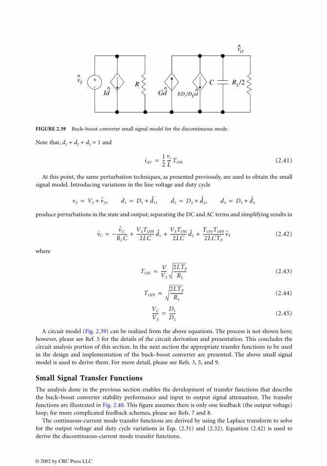
Note that, d1 + d2 + d3 = 1 and
(2.41)
At this point, the same perturbation techniques, as presented previously, are used to obtain the smallsignal model. Introducing variations in the line voltage and duty cycle
produce perturbations in the state and output; separating the DC and AC terms and simplifying results in
(2.42)
where
(2.43)
(2.44)
(2.45)
A circuit model (Fig. 2.39) can be realized from the above equations. The process is not shown here;however, please see Ref. 5 for the details of the circuit derivation and presentation. This concludes thecircuit analysis portion of this section. In the next section the appropriate transfer functions to be usedin the design and implementation of the buck–boost converter are presented. The above small signalmodel is used to derive them. For more detail, please see Refs. 3, 5, and 9.
Small Signal Transfer Functions
The analysis done in the previous section enables the development of transfer functions that describethe buck–boost converter stability performance and input to output signal attenuation. The transferfunctions are illustrated in Fig. 2.40. This figure assumes there is only one feedback (the output voltage)loop; for more complicated feedback schemes, please see Refs. 7 and 8.
The continuous-current mode transfer functions are derived by using the Laplace transform to solvefor the output voltage and duty cycle variations in Eqs. (2.31) and (2.32). Equation (2.42) is used toderive the discontinuous-current mode transfer functions.
FIGURE 2.39 Buck–boost converter small signal model for the discontinuous mode.
vO
vS+-
RL/2C^
Id ^I(D1/D2)d
^
RGd
2
iAV12--
vs
L---- TON=
vS VS vS, d1+ D1 d1 , d2+ D2 d2 , d3+ D3 d3+= = = =
vC −v C
RLC----------
VSTOFF
2LC---------------- d1
VSTON
2LC--------------- d2
TONTOFF
2LCTP
-------------------- vS+ + +=
TONVVS
-----2LTP
RL
------------=
TOFF
2LTP
RL
------------=
VC
VS
------D1
D2
------=
© 2002 by CRC Press LLC
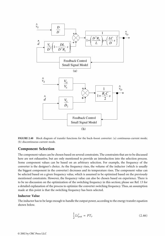
Component Selection
The component values can be chosen based on several constraints. The constraints that are to be discussedhere are not exhaustive, but are only mentioned to provide an introduction into the selection process.Some component values can be based on an arbitrary selection. For example, the frequency of theconverter is the designer’s choice. As the frequency rises, the volume of the inductor (which is usuallythe biggest component in the converter) decreases and its temperature rises. The component value canbe selected based on a given frequency value, which is assumed to be optimized based on the previouslymentioned constraints. However, the frequency value can also be chosen based on experience. There isto be no discussion on the optimization of the switching frequency in this section; please see Ref. 13 fora detailed explanation of the process to optimize the converter switching frequency. Thus, an assumptionmade at this point is that the switching frequency has been selected.
Inductor Value
The inductor has to be large enough to handle the output power, according to the energy transfer equationshown below.
(2.46)
FIGURE 2.40 Block diagram of transfer functions for the buck–boost converter: (a) continuous-current mode;(b) discontinuous-current mode.
’
−
2’2’1
2
’
3’
1
1
+
+ s
+
+
vS^
d^
vO^D
D
sRD
DL
D
V
L
S
sD
LC
L
RD L^
Feedback ControlSmall Signal Model
2
21
1
+
+
+
vS^
d^
vO^S
O
V
V
D
VS
sCRL
+
Feedback ControlSmall Signal Model
(a)
(b)
12-- Lipeak
2 PTP=
© 2002 by CRC Press LLC
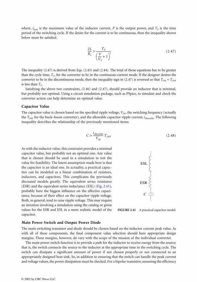
where, ipeak is the maximum value of the inductor current, P is the output power, and TP is the timeperiod of the switching cycle. If the desire for the current is to be continuous, then the inequality shownbelow must be satisfied.
(2.47)
The inequality (2.47) is derived from Eqs. (2.43) and (2.44). The total of those equations has to be greaterthan the cycle time, TP, for the converter to be in the continuous-current mode. If the designer desires theconverter to be in the discontinuous mode, then the inequality sign in (2.47) is reversed so that TON + TOFF
is less than TP.Satisfying the above two constraints, (2.46) and (2.47), should provide an inductor that is minimal,
but probably not optimal. Using a circuit simulation package, such as PSpice, to simulate and check theconverter action can help determine an optimal value.
Capacitor Value
The capacitor value is chosen based on the specified ripple voltage, VPP, the switching frequency (actuallythe TOFF for the buck–boost converter), and the allowable capacitor ripple current, iallowable. The followinginequality describes the relationship of the previously mentioned items:
(2.48)
As with the inductor value, this constraint provides a minimalcapacitor value, but probably not an optimal one. Any valuethat is chosen should be used in a simulation to test thevalue for feasibility. The latent assumption made here is thatthe capacitor is an ideal one. In actuality, a practical capac-itor can be modeled as a linear combination of resistors,inductors, and capacitors. This complicates the previouslydiscussed models greatly. The equivalent series resistance(ESR) and the equivalent series inductance (ESL) (Fig. 2.41),probably have the biggest influence on the effective capaci-tance, because of their effect on the capacitor ripple voltage.Both, in general, tend to raise ripple voltage. This may requirean iteration involving a simulation using the catalog or givenvalues for the ESR and ESL in a more realistic model of thecapacitor.
Main Power Switch and Output Power Diode
The main switching transistor and diode should be chosen based on the inductor current peak value. Aswith all of these components, the final component value selection should have appropriate designmargins. These margins, however, do vary with the scope of the mission of the individual converter.
The main power switch function is to provide a path for the inductor to receive energy from the source;that is, the switch connects the source to the inductor at the appropriate time in the switching cycle. Theswitch can dissipate a significant amount of power if not chosen properly or not connected to anappropriately designed heat sink. So, in addition to ensuring that the switch can handle the peak currentand voltage values, the power dissipation must be checked. For a bipolar transistor, assuming the efficiency
2LRL
------TP
VVS
----- 1+ 2---------------------->
Ciallowable
Vpp
--------------- TOFF>
FIGURE 2.41 A practical capacitor model.
ESR
C
ESL
© 2002 by CRC Press LLC

of the converter is very high, the on-state power dissipation can be expressed as the following:
(2.49)
where IO = P/VO . If a MOSFET device is chosen, the on-state dissipation is the following:
(2.50)
The output power diode provides the path for the inductor to discharge its energy to the output; itconnects the inductor to the output when the main power switch is off. Its voltage drop is primarilyresponsible for power dissipation. If Vd is the on-state voltage drop of the diode, then its power dissipationis expressed as
(2.51)
A judicious selection for the diode can be made using the above calculated power value, the peak outputcurrent, and output voltage.
Flyback Power Stage
A popular version of the buck–boost converter, shown in Fig. 2.28, is the variation shown in Fig. 2.42,the flyback converter. The flyback converter provides isolation from input to output: note the outputvoltage is not inverted as in the simpler buck–boost converter version of Fig. 2.28. These things areaccomplished because of the two-winding or coupled inductor. The inductor now serves a dual purpose:it transfers energy from the source to the output and provides input to output voltage. This is a popularpower stage used in off-line (110 VAC or 220 VAC) applications, particularly with multiple output voltages.Power diodes, capacitors, and windings on the two-winding inductor (power transformer) are added inthe appropriate fashion to provide additional outputs.
The process discussed previously can be used to determine the small signal model and DC operatingpoint of this converter. The state variables for this converter are the capacitor voltage, vC , and the fluxdensity, φ, of the two-winding inductor:
FIGURE 2.42 Flyback power converter.
PDISS VCEsatDD′------ IO
=
PDISSDD′------ IO
2
RDS on( )=
PDISS VDIO=
NPdφdt------ LP
didt----- and NS
dφdt------ LS
didt-----= =
vO
vS+- RL
C
NP :NS
+
-
Feedback Controland Drive Circuit
© 2002 by CRC Press LLC
The input voltage can be expressed as (NS /NP)vS , instead of just vs. Making these substitutions allowsthe development of the small signal model that is shown below.
The continuous-current mode small signal model is
(2.52)
(2.53)
with
(2.54)
and
(2.55)
The discontinuous-current mode small signal model is
(2.56)
with
(2.57)
(2.58)
(2.59)
Summary
This section has presented and analyzed a buck–boost converter (Fig. 2.28). The topological changes havebeen presented and a discussion of the state space has shown a modeling process (averaging), which canbe used to design the converter. This process models a linear time-varying structure in a relatively simpleway so that significant design insight can be obtained. The small signal model that was presented can beused to analyze the stability and the input-to-output signal attenuation of the buck–boost converter.
iL˙ D′vC
L-----------
DNS
NP
------ vS
L------------------
NS
NP
------ VS VC–
L-------------------------- d+ +=
vCD′C------
NS
LS
------ φvO
RLC----------
NS
LS
------ Φ
C------------ d+ +=
VO
VS
------NS
NP
------ DD′------=
ΦVO
D′RL
------------–LS
NS
------=
vCvC
RLC----------–
NS
NP
------ VSTOFF
2LSC------------------------- d1
NS
NP
------ VSTON
2LSC------------------------ d2
TONTOFF
2LSCTP
--------------------NS
NP
------ vS+ + +=
TONV
NS
NP
------ VS
--------------2LSTP
RL
--------------=
TOFF
2LSTP
RL
--------------=
VC
VS
------NS
NP
------D1
D2
------=
© 2002 by CRC Press LLC

References
1. Middlebrook, R. D. and Cúk, S., Modeling and analysis methods for DC-to-DC switching converters,presented at IEEE Int. Semiconductor Power Converter Conference, 1977.
2. Owen, H. A., Capel, A., and Ferrante, J. G., Simulation and analysis methods for sampled powerelectronic systems, in IEEE Power Electronics Specialists Conference Record, 1976, 45–55.
3. Wester, G. W. and Middlebrook, R. D., Low-frequency characterization of switched DC-DC convert-ers, IEEE Trans. Aerospace Electron. Syst., AES-9(3), 376–385, 1973.
4. Middlebrook R. D. and Cúk, S., A general unified approach to modeling switching-converter powerstages, in IEEE Power Electronics Specialists Conference Record, 1976, 18–34.
5. Cúk, S. and Middlebrook, R. D., A general unified approach to modeling switching DC-to-DC con-verters in discontinuous conduction mode, in IEEE Power Electronics Specialists Conference Record,1977, 36–57.
6. Lee, F. C. and Shortt, D. J., Improved model for predicting the dynamic performance of highbandwidth and multiloop power converters, in POWERCON 11 Record, 1984, E-3, 1–14.
7. Shortt, D. J. and Lee, F. C., Extensions of the discrete-average models for converter power stages, inPESC Record, 1983, 23–37; IEEE Trans. Aerospace Electron. Syst., AES-20(3), 279–289, 1984.
8. Shortt, D. J. and Lee, F. C., An improved switching converter model using discrete and averagetechniques, in PESC Record, 1982, 199–212; IEEE Trans. Aerospace Electron. Syst., AES-19(2), 1983.
9. Vorpérian, V., Tymerski, R., and Lee, F. C., Equivalent circuit models for resonant and PWM switches,IEEE Trans. Power Electron., 4(2), 1989.
10. Bello, V., Computer-aided analysis of switching regulators using SPICE2, in IEEE Power ElectronicsSpecialists Conference Record, 1980, 3–11.
11. Chen, D. Y., Owen, H. A., and Wilson, T. G., Computer-aided design and graphics applied to thestudy of inductor energy storage DC-to-DC electronic converters, IEEE Trans. Aerospace ElectronicSyst., AES-9(4), 585–597, 1973.
12. Lee, F. C., Yu, Y., and Triner, J. E., Modeling of switching regulator power stages with and withoutzero-inductor current dwell time, in IEEE Power Electronics Specialists Conference Record, 1976,62–72.
13. Rahman, S. and Lee, F. C., Nonlinear program based optimization of boost and buck–boost converterdesigns, in IEEE Power Electronics Specialists Conference Record, 1981, 180–191.
© 2002 by CRC Press LLC
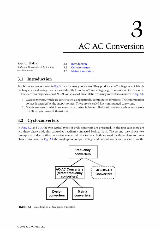
3AC-AC Conversion
3.1 Introduction3.2 Cycloconverters3.3 Matrix Converters
3.1 Introduction
AC-AC converters as shown in Fig. 3.1 are frequency converters. They produce an AC voltage in which boththe frequency and voltage can be varied directly from the AC line voltage, e.g., from a 60- or 50-Hz source.
There are two major classes of AC-AC, or so-called direct static frequency converters, as shown in Fig. 3.1.
1. Cycloconverters, which are constructed using naturally commutated thyristors. The commutationvoltage is ensured by the supply voltage. These are so-called line commutated converters.
2. Matrix converters, which are constructed using full-controlled static devices, such as transistorsor GTOs (gate turn-off thyristors).
3.2 Cycloconverters
In Figs. 3.2 and 3.3, the two typical types of cycloconverters are presented. In the first case there aretwo three-phase midpoint controlled rectifiers connected back to back. The second case shows twothree-phase bridge rectifier converters connected back to back. Both are used for three-phase to three-phase conversion. In Fig. 3.4 the single-phase output voltage and current waves are presented for the
FIGURE 3.1 Classification of frequency converters.
Frequencyconverters
AC-AC Converters(direct frequency
converters)
Cyclo-converters
Matrixconverters
AC-DC-ACConverters
Sándor HalászBudapest University of Technology and Economics
© 2002 by CRC Press LLC
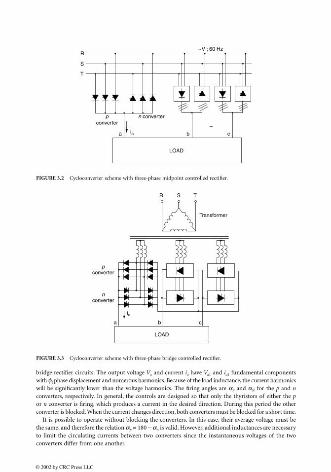
bridge rectifier circuits. The output voltage Va and current ia have Va1 and ia1 fundamental componentswith φ1 phase displacement and numerous harmonics. Because of the load inductance, the current harmonicswill be significantly lower than the voltage harmonics. The firing angles are αP and αN for the p and nconverters, respectively. In general, the controls are designed so that only the thyristors of either the por n converter is firing, which produces a current in the desired direction. During this period the otherconverter is blocked. When the current changes direction, both converters must be blocked for a short time.
It is possible to operate without blocking the converters. In this case, their average voltage must bethe same, and therefore the relation αp = 180 − αn is valid. However, additional inductances are necessaryto limit the circulating currents between two converters since the instantaneous voltages of the twoconverters differ from one another.
FIGURE 3.2 Cycloconverter scheme with three-phase midpoint controlled rectifier.
FIGURE 3.3 Cycloconverter scheme with three-phase bridge controlled rectifier.
pconverter
n converter
a b cia
R
S
T
LOAD
~V ; 60 Hz
−
R S T
Transformer
pconverter
nconverter
a
ia
b c
LOAD
© 2002 by CRC Press LLC
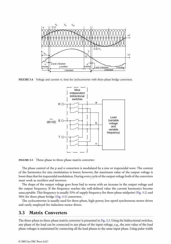
The phase control of the p and n converters is modulated by a sine or trapezoidal wave. The contentof the harmonics for sine modulation is lower; however, the maximum value of the output voltage islower than that for trapezoidal modulation. During every cycle of the output voltage both of the convertersmust work as rectifiers and inverters.
The shape of the output voltage goes from bad to worse with an increase in the output voltage andthe output frequency. If the frequency reaches the well-defined value the current harmonics becomeunacceptable. This frequency is usually 33% of supply frequency for three-phase midpoint (Fig. 3.2) and50% for three-phase bridge (Fig. 3.3) converters.
The cycloconverter is usually used for three-phase, high-power, low-speed synchronous motor drivesand rarely employed for induction motor drives.
3.3 Matrix Converters
The three-phase to three-phase matrix converter is presented in Fig. 3.5. Using the bidirectional switches,any phase of the load can be connected to any phase of the input voltage, e.g., the zero value of the loadphase voltages is maintained by connecting all the load phases to the same input phase. Using pulse-width
FIGURE 3.4 Voltage and current vs. time for cycloconverter with three-phase bridge converters.
FIGURE 3.5 Three-phase to three-phase matrix converter.
V
ia
ia1
ω1t
ω1t
αn
φ1
ninverter
pinverter
p and n blocked
p and n blockedp rectifier n rectifiern blocked p blocked
αp Va Va1
i
Nineindependentbidirectional
switches
Load(variablevoltage
andvariable
frequency)
R
S
T
c
b
a
(60 HZ)
© 2002 by CRC Press LLC

modulation techniques, the load voltage and the load frequency are controlled from zero to their max-imum values. The maximum voltage is usually close to the input voltage, but the maximum frequencycan be several times that of the input frequency and is only limited by practical considerations. Thebidirectional switches must be capable of permitting current flow in either direction. In Fig. 3.6 onepossible configuration of the bidirectional switch is shown.
Matrix converters require the use of numerous switches and well-established control methods. Someadditional elements are necessary for the safe commutation of the bidirectional switches. These disad-vantages of matrix converters prevent their use in industrial applications.
References
Guggi, L. and Pelly, B. R. 1976. Static Power Frequency Changes, John Wiley & Sons, New York. Pelly, B. R. 1976. Thyristor Phase-Controlled Converters, John Wiley & Sons, New York.
FIGURE 3.6 Bidirectional switch.
© 2002 by CRC Press LLC
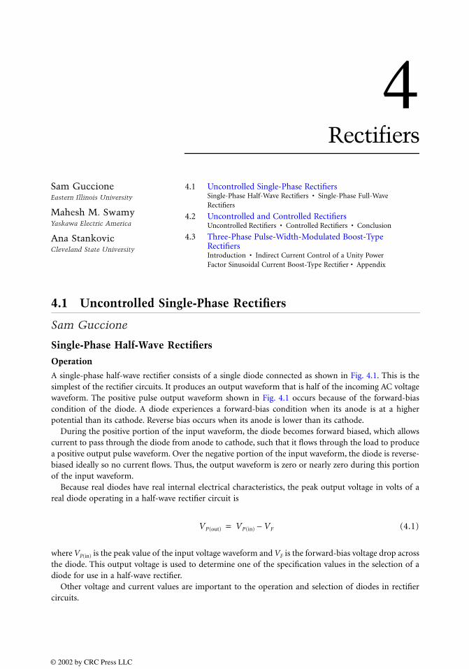
4Rectifiers
4.1 Uncontrolled Single-Phase RectifiersSingle-Phase Half-Wave Rectifiers • Single-Phase Full-Wave Rectifiers
4.2 Uncontrolled and Controlled RectifiersUncontrolled Rectifiers • Controlled Rectifiers • Conclusion
4.3 Three-Phase Pulse-Width-Modulated Boost-TypeRectifiersIntroduction • Indirect Current Control of a Unity Power Factor Sinusoidal Current Boost-Type Rectifier • Appendix
4.1 Uncontrolled Single-Phase Rectifiers
Sam Guccione
Single-Phase Half-Wave Rectifiers
Operation
A single-phase half-wave rectifier consists of a single diode connected as shown in Fig. 4.1. This is thesimplest of the rectifier circuits. It produces an output waveform that is half of the incoming AC voltagewaveform. The positive pulse output waveform shown in Fig. 4.1 occurs because of the forward-biascondition of the diode. A diode experiences a forward-bias condition when its anode is at a higherpotential than its cathode. Reverse bias occurs when its anode is lower than its cathode.
During the positive portion of the input waveform, the diode becomes forward biased, which allowscurrent to pass through the diode from anode to cathode, such that it flows through the load to producea positive output pulse waveform. Over the negative portion of the input waveform, the diode is reverse-biased ideally so no current flows. Thus, the output waveform is zero or nearly zero during this portionof the input waveform.
Because real diodes have real internal electrical characteristics, the peak output voltage in volts of areal diode operating in a half-wave rectifier circuit is
(4.1)
where VP(in) is the peak value of the input voltage waveform and VF is the forward-bias voltage drop acrossthe diode. This output voltage is used to determine one of the specification values in the selection of adiode for use in a half-wave rectifier.
Other voltage and current values are important to the operation and selection of diodes in rectifiercircuits.
VP(out) VP(in) VF–=
Sam GuccioneEastern Illinois University
Mahesh M. SwamyYaskawa Electric America
Ana StankovicCleveland State University
© 2002 by CRC Press LLC
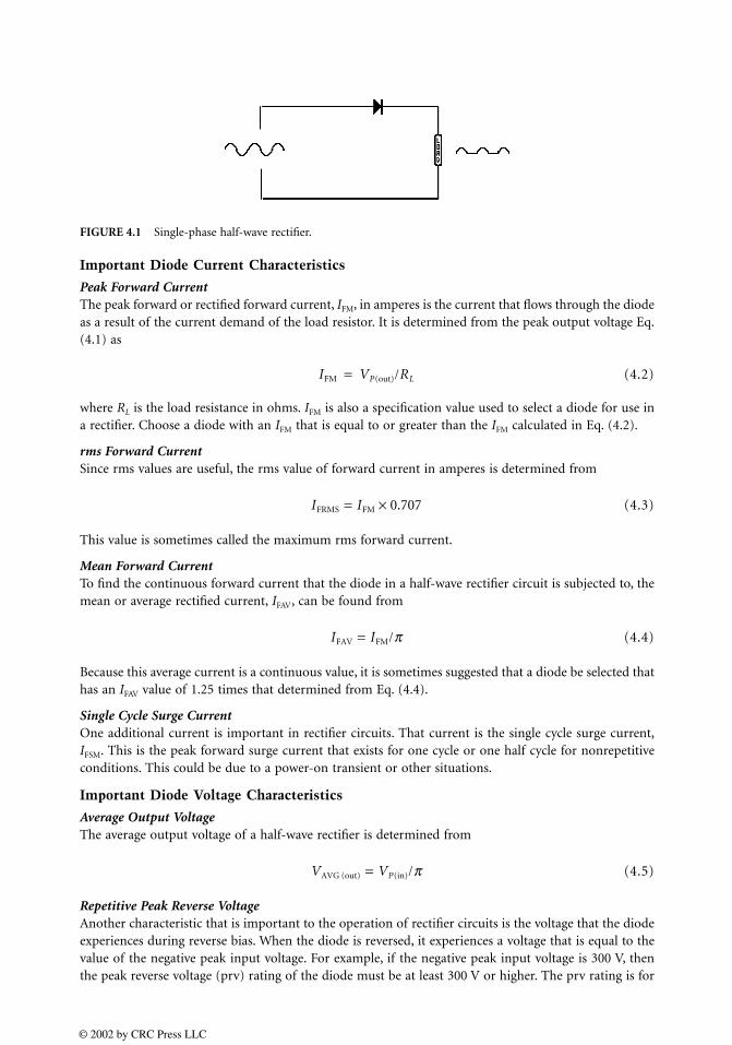
Important Diode Current Characteristics
Peak Forward CurrentThe peak forward or rectified forward current, IFM, in amperes is the current that flows through the diodeas a result of the current demand of the load resistor. It is determined from the peak output voltage Eq.(4.1) as
(4.2)
where RL is the load resistance in ohms. IFM is also a specification value used to select a diode for use ina rectifier. Choose a diode with an IFM that is equal to or greater than the IFM calculated in Eq. (4.2).
rms Forward CurrentSince rms values are useful, the rms value of forward current in amperes is determined from
(4.3)
This value is sometimes called the maximum rms forward current.
Mean Forward CurrentTo find the continuous forward current that the diode in a half-wave rectifier circuit is subjected to, themean or average rectified current, IFAV, can be found from
(4.4)
Because this average current is a continuous value, it is sometimes suggested that a diode be selected thathas an IFAV value of 1.25 times that determined from Eq. (4.4).
Single Cycle Surge CurrentOne additional current is important in rectifier circuits. That current is the single cycle surge current,IFSM. This is the peak forward surge current that exists for one cycle or one half cycle for nonrepetitiveconditions. This could be due to a power-on transient or other situations.
Important Diode Voltage Characteristics
Average Output VoltageThe average output voltage of a half-wave rectifier is determined from
(4.5)
Repetitive Peak Reverse VoltageAnother characteristic that is important to the operation of rectifier circuits is the voltage that the diodeexperiences during reverse bias. When the diode is reversed, it experiences a voltage that is equal to thevalue of the negative peak input voltage. For example, if the negative peak input voltage is 300 V, thenthe peak reverse voltage (prv) rating of the diode must be at least 300 V or higher. The prv rating is for
FIGURE 4.1 Single-phase half-wave rectifier.
IFM VP(out)/RL=
IFRMS IFM= 0.707×
IFAV IFM= /π
VAVG (out) VP(in)= /π
© 2002 by CRC Press LLC
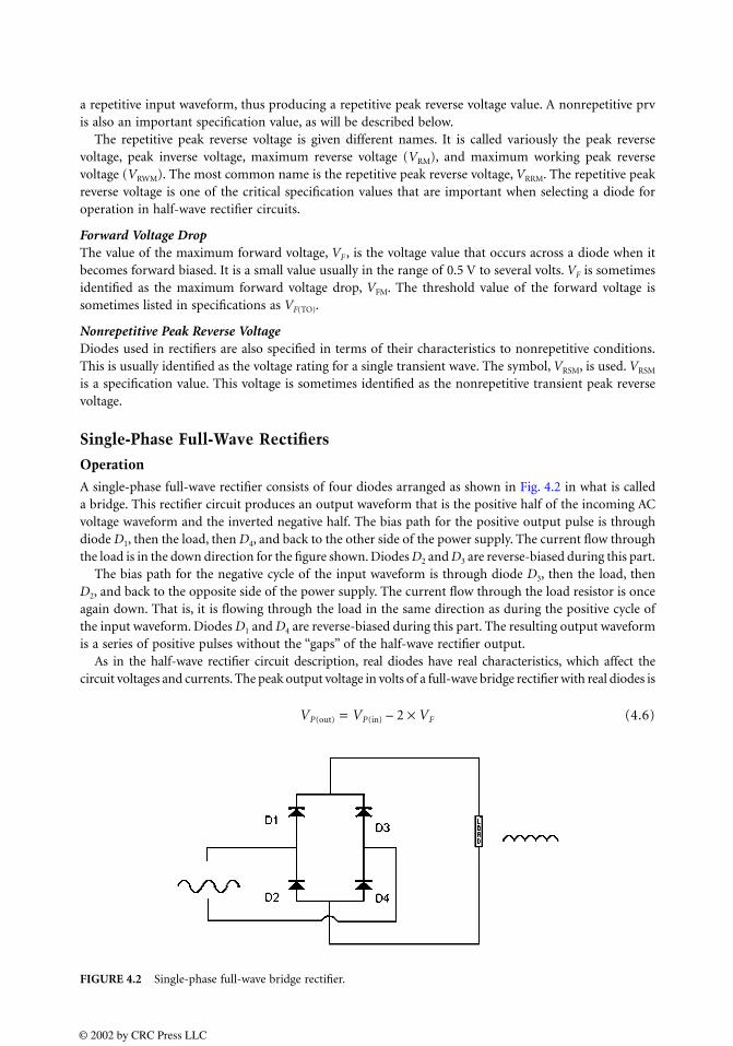
a repetitive input waveform, thus producing a repetitive peak reverse voltage value. A nonrepetitive prvis also an important specification value, as will be described below.
The repetitive peak reverse voltage is given different names. It is called variously the peak reversevoltage, peak inverse voltage, maximum reverse voltage (VRM), and maximum working peak reversevoltage (VRWM). The most common name is the repetitive peak reverse voltage, VRRM. The repetitive peakreverse voltage is one of the critical specification values that are important when selecting a diode foroperation in half-wave rectifier circuits.
Forward Voltage DropThe value of the maximum forward voltage, VF , is the voltage value that occurs across a diode when itbecomes forward biased. It is a small value usually in the range of 0.5 V to several volts. VF is sometimesidentified as the maximum forward voltage drop, VFM. The threshold value of the forward voltage issometimes listed in specifications as VF(TO).
Nonrepetitive Peak Reverse VoltageDiodes used in rectifiers are also specified in terms of their characteristics to nonrepetitive conditions.This is usually identified as the voltage rating for a single transient wave. The symbol, VRSM, is used. VRSM
is a specification value. This voltage is sometimes identified as the nonrepetitive transient peak reversevoltage.
Single-Phase Full-Wave Rectifiers
Operation
A single-phase full-wave rectifier consists of four diodes arranged as shown in Fig. 4.2 in what is calleda bridge. This rectifier circuit produces an output waveform that is the positive half of the incoming ACvoltage waveform and the inverted negative half. The bias path for the positive output pulse is throughdiode D1, then the load, then D4, and back to the other side of the power supply. The current flow throughthe load is in the down direction for the figure shown. Diodes D2 and D3 are reverse-biased during this part.
The bias path for the negative cycle of the input waveform is through diode D3, then the load, thenD2, and back to the opposite side of the power supply. The current flow through the load resistor is onceagain down. That is, it is flowing through the load in the same direction as during the positive cycle ofthe input waveform. Diodes D1 and D4 are reverse-biased during this part. The resulting output waveformis a series of positive pulses without the “gaps” of the half-wave rectifier output.
As in the half-wave rectifier circuit description, real diodes have real characteristics, which affect thecircuit voltages and currents. The peak output voltage in volts of a full-wave bridge rectifier with real diodes is
(4.6)
FIGURE 4.2 Single-phase full-wave bridge rectifier.
VP(out) VP(in)= 2 VF×–
© 2002 by CRC Press LLC
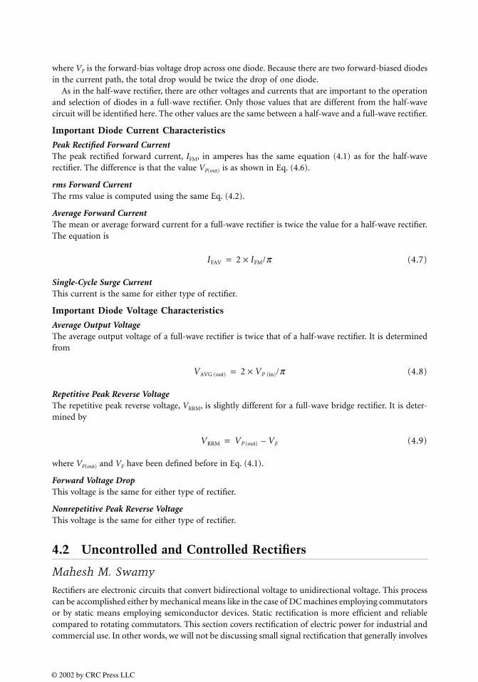
where VF is the forward-bias voltage drop across one diode. Because there are two forward-biased diodesin the current path, the total drop would be twice the drop of one diode.
As in the half-wave rectifier, there are other voltages and currents that are important to the operationand selection of diodes in a full-wave rectifier. Only those values that are different from the half-wavecircuit will be identified here. The other values are the same between a half-wave and a full-wave rectifier.
Important Diode Current Characteristics
Peak Rectified Forward CurrentThe peak rectified forward current, IFM, in amperes has the same equation (4.1) as for the half-waverectifier. The difference is that the value VP(out) is as shown in Eq. (4.6).
rms Forward CurrentThe rms value is computed using the same Eq. (4.2).
Average Forward CurrentThe mean or average forward current for a full-wave rectifier is twice the value for a half-wave rectifier.The equation is
(4.7)
Single-Cycle Surge CurrentThis current is the same for either type of rectifier.
Important Diode Voltage Characteristics
Average Output VoltageThe average output voltage of a full-wave rectifier is twice that of a half-wave rectifier. It is determinedfrom
(4.8)
Repetitive Peak Reverse VoltageThe repetitive peak reverse voltage, VRRM, is slightly different for a full-wave bridge rectifier. It is deter-mined by
(4.9)
where VP(out) and VF have been defined before in Eq. (4.1).
Forward Voltage DropThis voltage is the same for either type of rectifier.
Nonrepetitive Peak Reverse VoltageThis voltage is the same for either type of rectifier.
4.2 Uncontrolled and Controlled Rectifiers
Mahesh M. Swamy
Rectifiers are electronic circuits that convert bidirectional voltage to unidirectional voltage. This processcan be accomplished either by mechanical means like in the case of DC machines employing commutatorsor by static means employing semiconductor devices. Static rectification is more efficient and reliablecompared to rotating commutators. This section covers rectification of electric power for industrial andcommercial use. In other words, we will not be discussing small signal rectification that generally involves
IFAV 2 IFM/π×=
VAVG (out) 2 VP (in)× /π=
VRRM VP (out) VF–=
© 2002 by CRC Press LLC

low power and low voltage signals. Static power rectifiers can be classified into two broad groups. Theyare (1) uncontrolled rectifiers and (2) controlled rectifiers. Uncontrolled rectifiers make use of powersemiconductor diodes while controlled rectifiers make use of thyristors (SCRs), gate turn-off thyristors(GTOs), and MOSFET-controlled thyristors (MCTs).
Rectifiers, in general, are widely used in power electronics to rectify single-phase as well as three-phasevoltages. DC power supplies used in computers, consumer electronics, and a host of other applicationstypically make use of single-phase rectifiers. Industrial applications include, but are not limited to,industrial drives, metal extraction processes, industrial heating, power generation and transmission, etc.Most industrial applications of large power rating typically employ three-phase rectification processes.
Uncontrolled rectifiers in single-phase as well as in three-phase circuits will be discussed, as willcontrolled rectifiers. Application issues regarding uncontrolled and controlled rectifiers will be brieflydiscussed within each section.
Uncontrolled Rectifiers
The simplest uncontrolled rectifier use can be found in single-phase circuits. There are two types ofuncontrolled rectification. They are (1) half-wave rectification and (2) full-wave rectification. Half-waveand full-wave rectification techniques have been used in single-phase as well as in three-phase circuits.As mentioned earlier, uncontrolled rectifiers make use of diodes. Diodes are two-terminal semiconductordevices that allow flow of current in only one direction. The two terminals of a diode are known as theanode and the cathode.
Mechanics of Diode Conduction
The anode is formed when a pure semiconductor material, typically silicon, is doped with impuritiesthat have fewer valence electrons than silicon. Silicon has an atomic number of 14, which according toBohr’s atomic model means that the K and L shells are completely filled by 10 electrons and the remaining4 electrons occupy the M shell. The M shell can hold a maximum of 18 electrons. In a silicon crystal,every atom is bound to four other atoms, which are placed at the corners of a regular tetrahedron. Thebonding, which involves sharing of a valence electron with a neighboring atom is known as covalentbonding. When a Group 3 element (typically boron, aluminum, gallium, and indium) is doped into thesilicon lattice structure, three of the four covalent bonds are made. However, one bonding site is vacantin the silicon lattice structure. This creates vacancies or holes in the semiconductor. In the presence ofeither a thermal field or an electrical field, electrons from a neighboring lattice or from an external agencytend to migrate to fill this vacancy. The vacancy or hole can also be said to move toward the approachingelectron, thereby creating a mobile hole and hence current flow. Such a semiconductor material is alsoknown as lightly doped semiconductor material or p-type. Similarly, the cathode is formed when siliconis doped with impurities that have higher valence electrons than silicon. This would mean elementsbelonging to Group 5. Typical doping impurities of this group are phosphorus, arsenic, and antimony.When a Group 5 element is doped into the silicon lattice structure, it oversatisfies the covalent bondingsites available in the silicon lattice structure, creating excess or loose electrons in the valence shell. In thepresence of either a thermal field or an electrical field, these loose electrons easily get detached from thelattice structure and are free to conduct electricity. Such a semiconductor material is also known as heavilydoped semiconductor material or n-type.
The structure of the final doped crystal even after the addition of acceptor impurities (Group 3) ordonor impurities (Group 5), remains electrically neutral. The available electrons balance the net positivecharge and there is no charge imbalance.
When a p-type material is joined with an n-type material, a pn-junction is formed. Some loose electronsfrom the n-type material migrate to fill the holes in the p-type material and some holes in the p-typemigrate to meet with the loose electrons in the n-type material. Such a movement causes the p-type struc-ture to develop a slight negative charge and the n-type structure to develop some positive charge.These slight positive and negative charges in the n-type and p-type areas, respectively, prevent further
© 2002 by CRC Press LLC
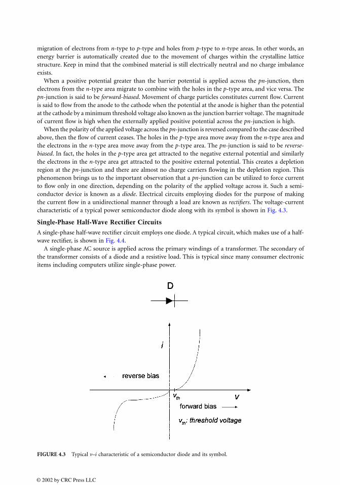
migration of electrons from n-type to p-type and holes from p-type to n-type areas. In other words, anenergy barrier is automatically created due to the movement of charges within the crystalline latticestructure. Keep in mind that the combined material is still electrically neutral and no charge imbalanceexists.
When a positive potential greater than the barrier potential is applied across the pn-junction, thenelectrons from the n-type area migrate to combine with the holes in the p-type area, and vice versa. Thepn-junction is said to be forward-biased. Movement of charge particles constitutes current flow. Currentis said to flow from the anode to the cathode when the potential at the anode is higher than the potentialat the cathode by a minimum threshold voltage also known as the junction barrier voltage. The magnitudeof current flow is high when the externally applied positive potential across the pn-junction is high.
When the polarity of the applied voltage across the pn-junction is reversed compared to the case describedabove, then the flow of current ceases. The holes in the p-type area move away from the n-type area andthe electrons in the n-type area move away from the p-type area. The pn-junction is said to be reverse-biased. In fact, the holes in the p-type area get attracted to the negative external potential and similarlythe electrons in the n-type area get attracted to the positive external potential. This creates a depletionregion at the pn-junction and there are almost no charge carriers flowing in the depletion region. Thisphenomenon brings us to the important observation that a pn-junction can be utilized to force currentto flow only in one direction, depending on the polarity of the applied voltage across it. Such a semi-conductor device is known as a diode. Electrical circuits employing diodes for the purpose of makingthe current flow in a unidirectional manner through a load are known as rectifiers. The voltage-currentcharacteristic of a typical power semiconductor diode along with its symbol is shown in Fig. 4.3.
Single-Phase Half-Wave Rectifier Circuits
A single-phase half-wave rectifier circuit employs one diode. A typical circuit, which makes use of a half-wave rectifier, is shown in Fig. 4.4.
A single-phase AC source is applied across the primary windings of a transformer. The secondary ofthe transformer consists of a diode and a resistive load. This is typical since many consumer electronicitems including computers utilize single-phase power.
FIGURE 4.3 Typical v–i characteristic of a semiconductor diode and its symbol.
© 2002 by CRC Press LLC
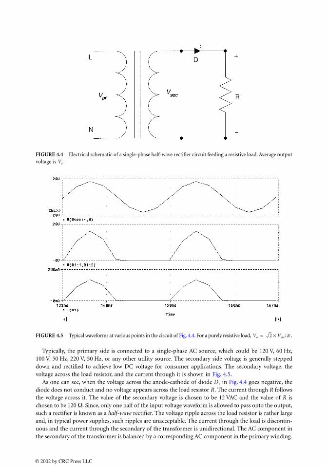
Typically, the primary side is connected to a single-phase AC source, which could be 120 V, 60 Hz,100 V, 50 Hz, 220 V, 50 Hz, or any other utility source. The secondary side voltage is generally steppeddown and rectified to achieve low DC voltage for consumer applications. The secondary voltage, thevoltage across the load resistor, and the current through it is shown in Fig. 4.5.
As one can see, when the voltage across the anode-cathode of diode D1 in Fig. 4.4 goes negative, thediode does not conduct and no voltage appears across the load resistor R. The current through R followsthe voltage across it. The value of the secondary voltage is chosen to be 12 VAC and the value of R ischosen to be 120 Ω. Since, only one half of the input voltage waveform is allowed to pass onto the output,such a rectifier is known as a half-wave rectifier. The voltage ripple across the load resistor is rather largeand, in typical power supplies, such ripples are unacceptable. The current through the load is discontin-uous and the current through the secondary of the transformer is unidirectional. The AC component inthe secondary of the transformer is balanced by a corresponding AC component in the primary winding.
FIGURE 4.4 Electrical schematic of a single-phase half-wave rectifier circuit feeding a resistive load. Average outputvoltage is Vo.
FIGURE 4.5 Typical waveforms at various points in the circuit of Fig. 4.4. For a purely resistive load, .Vo 2 Vsec× /π=
© 2002 by CRC Press LLC
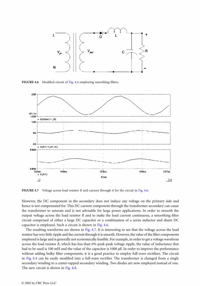
However, the DC component in the secondary does not induce any voltage on the primary side andhence is not compensated for. This DC current component through the transformer secondary can causethe transformer to saturate and is not advisable for large power applications. In order to smooth theoutput voltage across the load resistor R and to make the load current continuous, a smoothing filtercircuit comprised of either a large DC capacitor or a combination of a series inductor and shunt DCcapacitor is employed. Such a circuit is shown in Fig. 4.6.
The resulting waveforms are shown in Fig. 4.7. It is interesting to see that the voltage across the loadresistor has very little ripple and the current through it is smooth. However, the value of the filter componentsemployed is large and is generally not economically feasible. For example, in order to get a voltage waveformacross the load resistor R, which has less than 6% peak-peak voltage ripple, the value of inductance thathad to be used is 100 mH and the value of the capacitor is 1000 µF. In order to improve the performancewithout adding bulky filter components, it is a good practice to employ full-wave rectifiers. The circuitin Fig. 4.4 can be easily modified into a full-wave rectifier. The transformer is changed from a singlesecondary winding to a center-tapped secondary winding. Two diodes are now employed instead of one.The new circuit is shown in Fig. 4.8.
FIGURE 4.6 Modified circuit of Fig. 4.4 employing smoothing filters.
FIGURE 4.7 Voltage across load resistor R and current through it for the circuit in Fig. 4.6.
© 2002 by CRC Press LLC
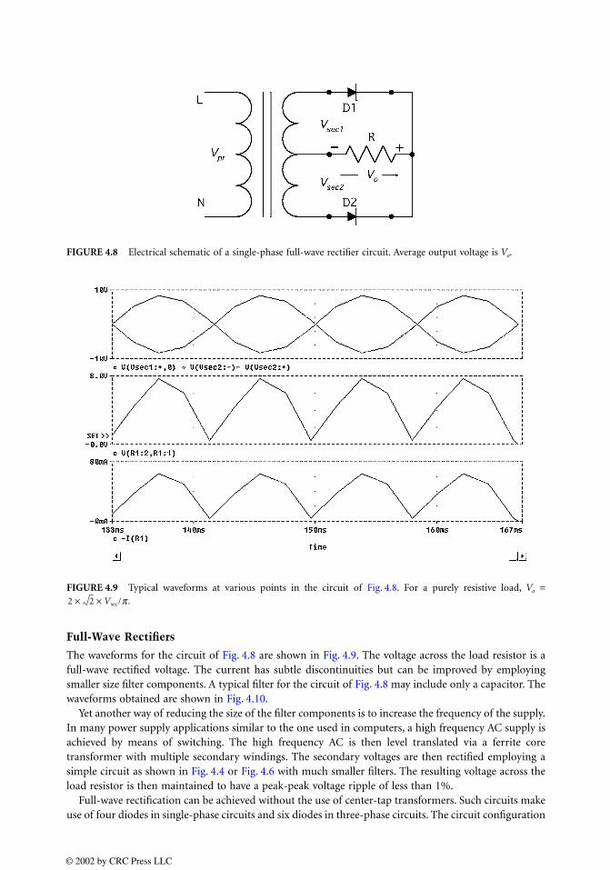
Full-Wave Rectifiers
The waveforms for the circuit of Fig. 4.8 are shown in Fig. 4.9. The voltage across the load resistor is afull-wave rectified voltage. The current has subtle discontinuities but can be improved by employingsmaller size filter components. A typical filter for the circuit of Fig. 4.8 may include only a capacitor. Thewaveforms obtained are shown in Fig. 4.10.
Yet another way of reducing the size of the filter components is to increase the frequency of the supply.In many power supply applications similar to the one used in computers, a high frequency AC supply isachieved by means of switching. The high frequency AC is then level translated via a ferrite coretransformer with multiple secondary windings. The secondary voltages are then rectified employing asimple circuit as shown in Fig. 4.4 or Fig. 4.6 with much smaller filters. The resulting voltage across theload resistor is then maintained to have a peak-peak voltage ripple of less than 1%.
Full-wave rectification can be achieved without the use of center-tap transformers. Such circuits makeuse of four diodes in single-phase circuits and six diodes in three-phase circuits. The circuit configuration
FIGURE 4.8 Electrical schematic of a single-phase full-wave rectifier circuit. Average output voltage is Vo.
FIGURE 4.9 Typical waveforms at various points in the circuit of Fig. 4.8. For a purely resistive load, Vo =2 2× Vsec× /π .
© 2002 by CRC Press LLC
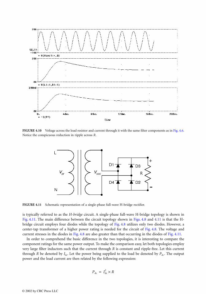
is typically referred to as the H-bridge circuit. A single-phase full-wave H-bridge topology is shown inFig. 4.11. The main difference between the circuit topology shown in Figs. 4.8 and 4.11 is that the H-bridge circuit employs four diodes while the topology of Fig. 4.8 utilizes only two diodes. However, acenter-tap transformer of a higher power rating is needed for the circuit of Fig. 4.8. The voltage andcurrent stresses in the diodes in Fig. 4.8 are also greater than that occurring in the diodes of Fig. 4.11.
In order to comprehend the basic difference in the two topologies, it is interesting to compare thecomponent ratings for the same power output. To make the comparison easy, let both topologies employvery large filter inductors such that the current through R is constant and ripple-free. Let this currentthrough R be denoted by Idc. Let the power being supplied to the load be denoted by Pdc . The outputpower and the load current are then related by the following expression:
FIGURE 4.10 Voltage across the load resistor and current through it with the same filter components as in Fig. 4.6.Notice the conspicuous reduction in ripple across R.
FIGURE 4.11 Schematic representation of a single-phase full-wave H-bridge rectifier.
Pdc Idc2 R×=
© 2002 by CRC Press LLC
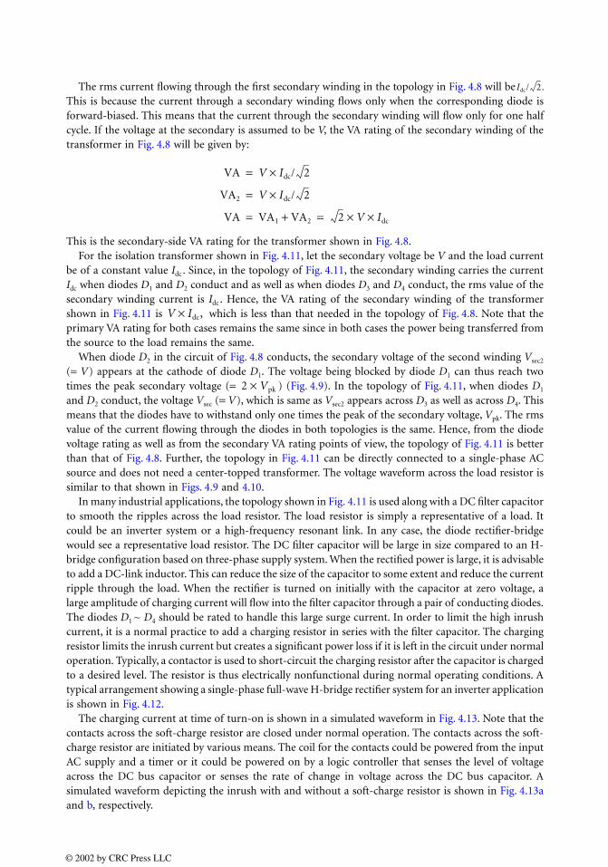
The rms current flowing through the first secondary winding in the topology in Fig. 4.8 will beThis is because the current through a secondary winding flows only when the corresponding diode isforward-biased. This means that the current through the secondary winding will flow only for one halfcycle. If the voltage at the secondary is assumed to be V, the VA rating of the secondary winding of thetransformer in Fig. 4.8 will be given by:
This is the secondary-side VA rating for the transformer shown in Fig. 4.8.For the isolation transformer shown in Fig. 4.11, let the secondary voltage be V and the load current
be of a constant value Idc . Since, in the topology of Fig. 4.11, the secondary winding carries the currentIdc when diodes D1 and D2 conduct and as well as when diodes D3 and D4 conduct, the rms value of thesecondary winding current is Idc . Hence, the VA rating of the secondary winding of the transformershown in Fig. 4.11 is which is less than that needed in the topology of Fig. 4.8. Note that theprimary VA rating for both cases remains the same since in both cases the power being transferred fromthe source to the load remains the same.
When diode D2 in the circuit of Fig. 4.8 conducts, the secondary voltage of the second winding Vsec2
(= V) appears at the cathode of diode D1. The voltage being blocked by diode D1 can thus reach twotimes the peak secondary voltage (= ) (Fig. 4.9). In the topology of Fig. 4.11, when diodes D1
and D2 conduct, the voltage Vsec (= V), which is same as Vsec2 appears across D3 as well as across D4. Thismeans that the diodes have to withstand only one times the peak of the secondary voltage, Vpk. The rmsvalue of the current flowing through the diodes in both topologies is the same. Hence, from the diodevoltage rating as well as from the secondary VA rating points of view, the topology of Fig. 4.11 is betterthan that of Fig. 4.8. Further, the topology in Fig. 4.11 can be directly connected to a single-phase ACsource and does not need a center-topped transformer. The voltage waveform across the load resistor issimilar to that shown in Figs. 4.9 and 4.10.
In many industrial applications, the topology shown in Fig. 4.11 is used along with a DC filter capacitorto smooth the ripples across the load resistor. The load resistor is simply a representative of a load. Itcould be an inverter system or a high-frequency resonant link. In any case, the diode rectifier-bridgewould see a representative load resistor. The DC filter capacitor will be large in size compared to an H-bridge configuration based on three-phase supply system. When the rectified power is large, it is advisableto add a DC-link inductor. This can reduce the size of the capacitor to some extent and reduce the currentripple through the load. When the rectifier is turned on initially with the capacitor at zero voltage, alarge amplitude of charging current will flow into the filter capacitor through a pair of conducting diodes.The diodes D1 ∼ D4 should be rated to handle this large surge current. In order to limit the high inrushcurrent, it is a normal practice to add a charging resistor in series with the filter capacitor. The chargingresistor limits the inrush current but creates a significant power loss if it is left in the circuit under normaloperation. Typically, a contactor is used to short-circuit the charging resistor after the capacitor is chargedto a desired level. The resistor is thus electrically nonfunctional during normal operating conditions. Atypical arrangement showing a single-phase full-wave H-bridge rectifier system for an inverter applicationis shown in Fig. 4.12.
The charging current at time of turn-on is shown in a simulated waveform in Fig. 4.13. Note that thecontacts across the soft-charge resistor are closed under normal operation. The contacts across the soft-charge resistor are initiated by various means. The coil for the contacts could be powered from the inputAC supply and a timer or it could be powered on by a logic controller that senses the level of voltageacross the DC bus capacitor or senses the rate of change in voltage across the DC bus capacitor. Asimulated waveform depicting the inrush with and without a soft-charge resistor is shown in Fig. 4.13aand b, respectively.
Idc/ 2.
VA V Idc× / 2=
VA2 V Idc× / 2=
VA VA1 VA2+ 2 V Idc××= =
V Idc× ,
2 Vpk×
© 2002 by CRC Press LLC

For larger power applications, typically above 1.5 kW, it is advisable to use a higher power supply. Insome applications, two of the three phases of a three-phase power system are used as the source poweringthe rectifier of Fig. 4.11 The line-line voltage could be either 240 or 480 VAC. Under those circumstances,one may go up to 10 kW of load power before adopting a full three-phase H-bridge configuration. Beyond10 kW, the size of the capacitor becomes too large to achieve a peak-peak voltage ripple of less than 5%.Hence, it is advisable then to employ three-phase rectifier configurations.
Three-Phase Rectifiers (Half-Wave and Full-Wave)
Similar to the single-phase case, there exist half-wave and full-wave three-phase rectifier circuits. Again,similar to the single-phase case, the half-wave rectifier in the three-phase case also yields DC componentsin the source current. The source has to be large enough to handle this. Therefore, it is not advisable touse three-phase half-wave rectifier topology for large power applications. The three-phase half-waverectifier employs three diodes while the full-wave H-bridge configuration employs six diodes. Typicalthree-phase half-wave and full-wave topologies are shown in Fig. 4.14.
In the half-wave rectifier shown in Fig. 4.14a, the shape of the output voltage and current through theresistive load is dictated by the instantaneous value of the source voltages, L1, L2, and L3. These sourcevoltages are phase shifted in time by 120 electrical degrees, which corresponds to approximately 5.55 msfor a 60 Hz system. This means that if one considers the L1 phase to reach its peak value at time t1, theL2 phase will achieve its peak 120 electrical degrees later (t1 + 5.55 ms), and L3 will achieve its peak 120electrical degrees later than L2 (t1 + 5.55 ms + 5.55 ms). Since all three phases are connected to the sameoutput resistor R, the phase that provides the highest instantaneous voltage is the phase that appearsacross R. In other words, the phase with the highest instantaneous voltage reverse biases the diodes ofthe other two phases and prevents them from conducting, which consequently prevents those phasevoltages from appearing across R. Since a particular phase is connected to only one diode in Fig. 4.14a,only three pulses, each of 120° duration, appear across the load resistor, R. Typical output voltage acrossR for the circuit of Fig. 4.14a is shown in Fig. 4.15a.
A similar explanation can be provided to explain the voltage waveform across a purely resistive loadin the case of the three-phase full-wave rectifier shown in Fig. 4.14b. The output voltage that appearsacross R is the highest instantaneous line-line voltage and not simply the phase voltage. Since there aresix such intervals, each of 60 electrical degrees duration in a given cycle, the output voltage waveformwill have six pulses in one cycle (Fig. 4.15b). Since a phase is connected to two diodes (diode pair), eachphase conducts current out and into itself, thereby eliminating the DC component in one complete cycle.
The waveform for a three-phase full-wave rectifier with a purely resistive load is shown in Fig. 4.15b.Note that the number of humps in Fig. 4.15a is only three in one AC cycle, while the number of humpsin Fig. 4.15b is six in one AC cycle.
In both the configurations shown in Fig. 4.14, the load current does not become discontinuous dueto three-phase operation. Comparing this to the single-phase half-wave and full-wave rectifier, one cansay that the output voltage ripple is much lower in three-phase rectifier systems compared to single-phase
FIGURE 4.12 Single-phase H-bridge circuit for use with power electronic circuits.
© 2002 by CRC Press LLC
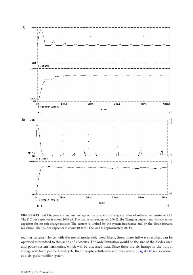
rectifier systems. Hence, with the use of moderately sized filters, three-phase full-wave rectifiers can beoperated at hundred to thousands of kilowatts. The only limitation would be the size of the diodes usedand power system harmonics, which will be discussed next. Since there are six humps in the outputvoltage waveform per electrical cycle, the three-phase full-wave rectifier shown in Fig. 4.14b is also knownas a six-pulse rectifier system.
FIGURE 4.13 (a) Charging current and voltage across capacitor for a typical value of soft-charge resistor of 2 Ω.The DC bus capacitor is about 1000 µF. The load is approximately 200 Ω. (b) Charging current and voltage acrosscapacitor for no soft charge resistor. The current is limited by the system impedance and by the diode forwardresistance. The DC bus capacitor is about 1000 µF. The load is approximately 200 Ω.
© 2002 by CRC Press LLC
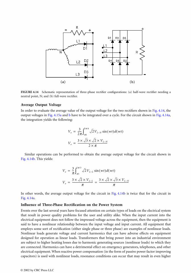
Average Output Voltage
In order to evaluate the average value of the output voltage for the two rectifiers shown in Fig. 4.14, theoutput voltages in Fig. 4.15a and b have to be integrated over a cycle. For the circuit shown in Fig. 4.14a,the integration yields the following:
Similar operations can be performed to obtain the average output voltage for the circuit shown inFig. 4.14b. This yields:
In other words, the average output voltage for the circuit in Fig. 4.14b is twice that for the circuit inFig. 4.14a.
Influence of Three-Phase Rectification on the Power System
Events over the last several years have focused attention on certain types of loads on the electrical systemthat result in power quality problems for the user and utility alike. When the input current into theelectrical equipment does not follow the impressed voltage across the equipment, then the equipment issaid to have a nonlinear relationship between the input voltage and input current. All equipment thatemploys some sort of rectification (either single phase or three phase) are examples of nonlinear loads.Nonlinear loads generate voltage and current harmonics that can have adverse effects on equipmentdesigned for operation as linear loads. Transformers that bring power into an industrial environmentare subject to higher heating losses due to harmonic generating sources (nonlinear loads) to which theyare connected. Harmonics can have a detrimental effect on emergency generators, telephones, and otherelectrical equipment. When reactive power compensation (in the form of passive power factor improvingcapacitors) is used with nonlinear loads, resonance conditions can occur that may result in even higher
FIGURE 4.14 Schematic representation of three-phase rectifier configurations: (a) half-wave rectifier needing aneutral point, N; and (b) full-wave rectifier.
Vo3
2π------ 2VL−N
π6
5π/6
∫ wt( )d wt( )sin=
Vo
3 3× 2 VL−N××2 π×
-----------------------------------------------=
Vo3π--- 2VL−L
π3
2π/3
∫ wt( )d wt( )sin=
Vo
3 2× VL−L×π
---------------------------------3 2 3 VL−N×××
π-----------------------------------------------= =
© 2002 by CRC Press LLC
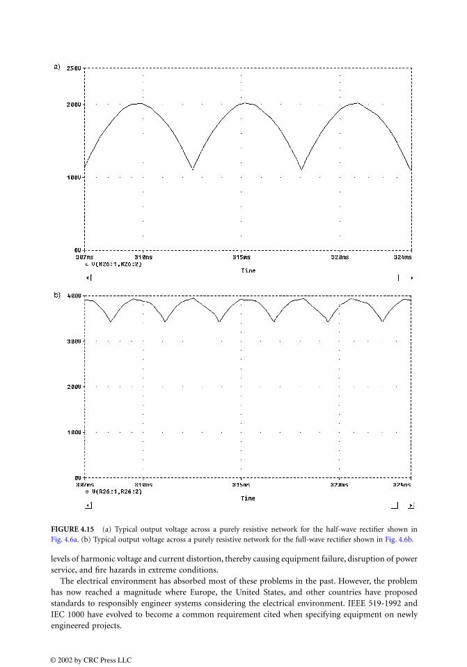
levels of harmonic voltage and current distortion, thereby causing equipment failure, disruption of powerservice, and fire hazards in extreme conditions.
The electrical environment has absorbed most of these problems in the past. However, the problemhas now reached a magnitude where Europe, the United States, and other countries have proposedstandards to responsibly engineer systems considering the electrical environment. IEEE 519-1992 andIEC 1000 have evolved to become a common requirement cited when specifying equipment on newlyengineered projects.
FIGURE 4.15 (a) Typical output voltage across a purely resistive network for the half-wave rectifier shown inFig. 4.6a. (b) Typical output voltage across a purely resistive network for the full-wave rectifier shown in Fig. 4.6b.
© 2002 by CRC Press LLC

Why Diode Rectifiers Generate HarmonicsThe current waveform at the inputs of a three-phase full-wave rectifier is not continuous. It has multiplezero crossings in one electrical cycle. The current harmonics generated by rectifiers having DC buscapacitors are caused by the pulsed current pattern at the input. The DC bus capacitor draws chargingcurrent only when it gets discharged due to the load. The charging current flows into the capacitor whenthe input rectifier is forward-biased, which occurs when the instantaneous input voltage is higher thanthe steady-state DC voltage across the DC bus capacitor. The pulsed current drawn by the DC bus capacitoris rich in harmonics due to the fact that it is discontinuous as shown in Fig. 4.16. Sometimes there arealso voltage harmonics that are associated with three-phase rectifier systems. The voltage harmonicsgenerated by three-phase rectifiers are due to the flat-topping effect caused by a weak AC source chargingthe DC bus capacitor without any intervening impedance. The distorted voltage waveform gives rise tovoltage harmonics that could lead to possible network resonance.
The order of current harmonics produced by a semiconductor converter during normal operation istermed characteristic harmonics. In a three-phase, six-pulse rectifier with no DC bus capacitor, thecharacteristic harmonics are nontriplen odd harmonics (e.g., 5th, 7th, 11th, etc.). In general, the char-acteristic harmonics generated by a semiconductor recitifier are given by:
where h is the order of harmonics; k is any integer, and q is the pulse number of the semiconductorrectifier (six for a six-pulse rectifier). When operating a six-pulse rectifier system with a DC bus capacitor(as in voltage source inverters, or VSI), one may start observing harmonics of orders other than thosegiven by the above equation. Such harmonics are called noncharacteristic harmonics. Though of lowermagnitude, these also contribute to the overall harmonic distortion of the input current. The per-unitvalue of the characteristic harmonics present in the theoretical current waveform at the input of thesemiconductor converter is given by 1/h, where h is the order of the harmonics. In practice, the observedper-unit value of the harmonics is much greater than 1/h. This is because the theoretical current waveform
FIGURE 4.16 Typical pulsed-current waveform as seen at input of a three-phase diode rectifier with DC capacitorfilter. The lower trace is input line-line voltage.
h kq 1±=
© 2002 by CRC Press LLC
is a rectangular pattern made up of equal positive and negative halves, each occupying 120 electricaldegrees. The pulsed discontinuous waveform observed commonly at the input of a three-phase full-waverectifier system depends greatly on the impedance of the power system, the size of the DC bus capacitors,and the level of loading of the DC bus capacitors. Total harmonic current distortion is defined as:
where I1 is the rms value of the fundamental component of current; and In is the rms value of the nthharmonic component of current.
Harmonic Limits Based on IEEE Std. 519-1992The IEEE Std. 519-1992 relies strongly on the definition of the point of common coupling or PCC. ThePCC from the utility viewpoint will usually be the point where power comes into the establishment (i.e.,point of metering). However, IEEE Std. 519-1992 also suggests that “within an industrial plant, thepoint of common coupling (PCC) is the point between the nonlinear load and other loads” (IEEE Std.519-1992). This suggestion is crucial since many plant managers and building supervisors feel that it isequally, if not more important to keep the harmonic levels at or below acceptable guidelines within theirfacility. In view of the many recently reported problems associated with harmonics within industrialplants, it is important to recognize the need for mitigating harmonics at the point where the offendingequipment is connected to the power system. This approach would minimize harmonic problems, therebyreducing costly downtime and improving the life of electrical equipment. If one is successful in mitigatingindividual load current harmonics, then the total harmonics at the point of the utility connection willin most cases meet or exceed the IEEE recommended guidelines. In view of this, it is becoming increasinglycommon for specifiers to require nonlinear equipment suppliers to adopt the procedure outlined in IEEEStd. 519-1992 to mitigate the harmonics to acceptable levels at the point of the offending equipment.For this to be interpreted equally by different suppliers, the intended PCC must be identified. If the PCCis not defined clearly, many suppliers of offending equipment would likely adopt the PCC at the utilitymetering point, which would not benefit the plant or the building, but rather the utility.
Having established that it is beneficial to adopt the PCC to be the point where the nonlinear equipmentconnects to the power system, the next step is to establish the short circuit ratio. Short circuit ratiocalculations are key in establishing the allowable current harmonic distortion levels. For calculating theshort circuit ratio, one has to determine the available short circuit current at the input terminals of thenonlinear equipment. The short-circuit current available at the input of nonlinear equipment can becalculated by knowing the value of the short-circuit current available at the secondary of the utilitytransformer supplying power to the establishment (building) and the series impedance in the electricalcircuit between the secondary of the transformer and the nonlinear equipment. In practice, it is commonto assume the same short circuit current level as at the secondary of the utility transformer feedingthe nonlinear equipment. The next step is to compute the fundamental value of the rated input currentinto the nonlinear equipment (three-phase full-wave rectifier in this case). An example is presented hereto recap the above procedure. A widely used industrial equipment item that employs a three-phase full-wave rectifier is the voltage source inverter (VSI). These are used for controlling speed and torque ofinduction motors. Such equipment is also known as an Adjustable Speed Drive (ASD) or Variable FrequencyDrive (VFD).
A 100-hp ASD/motor combination connected to a 480-V system being fed from a 1500-kVA, three-phase transformer with impedance of 4% is required to meet IEEE Std. 519-1992 at its input terminals.The rated current of the transformer is and is calculated to be 1804.2 A.The short-circuit current available at the secondary of the transformer is equal to the rated current dividedby the per unit impedance of the transformer. This is calculated to be 45,105.5 A. The short-circuit ratio,
THDI
In2
n=2
n=∞
∑I1
----------------=
1500 1000/(√(3) 480× )× ,
© 2002 by CRC Press LLC

which is defined as the ratio of the short-circuit current at the PCC to the fundamental value of thenonlinear current is computed next. NEC amps for 100-hp, 460-V is 124 A. Assuming that the short-circuit current at the ASD input is practically the same as that at the secondary of the utility transformer,the short-circuit ratio is calculated to be: 45,105.5/124, which equals 363.75. On referring to IEEE Std.519-1992, Table 10.3 (IEEE Std. 519-1992), the short-circuit ratio falls in the 100 to 1000 category. Forthis ratio, the total demand distortion (TDD) at the point of ASD connection to the power system networkis recommended to be 15% or less. For reference, see Table 4.1.
Harmonic Mitigating TechniquesVarious techniques of improving the input current waveform are discussed below. The intent of alltechniques is to make the input current more continuous so as to reduce the overall current harmonicdistortion. The different techniques can be classified into four broad categories:
1. Introduction of line reactors and/or DC link chokes2. Passive filters (series, shunt, and low pass broadband filters)3. Phase multiplication (12-pulse, 18-pulse rectifier systems)4. Active harmonic compensation
The following paragraphs will briefly discuss the available technologies and their relative advantages anddisadvantages. The term three-phase line reactor or just reactor is used in the following paragraphs todenote three-phase line inductors.
Three-Phase Line ReactorsLine reactors offer a significant magnitude of inductance that can alter the way the current is drawn bya nonlinear load such as a rectifier bridge. The reactor makes the current waveform less discontinuous,resulting in lower current harmonics. Since the reactor impedance increases with frequency, it offerslarger impedance to the flow of higher order harmonic currents. Therefore, it is instrumental in impedinghigher frequency current components while allowing the fundamental frequency component to passthrough with relative ease.
On knowing the input reactance value, one can estimate the expected current harmonic distortion. Atable illustrating the typically expected input current harmonics for various amounts of input reactanceis shown in Table 4.2.
Input reactance is determined by the accumulated impedance of the AC reactor, DC link choke (ifused), input transformer, and cable impedance. To maximize the input reactance while minimizing AC
TABLE 4.1 Current Distortion Limits for General Distribution Systems
(120 V through 69,000 V)Maximum Harmonic Current Distortion in percent of IL
Individual Harmonic Order (Odd Harmonics)a
Isc /IL <11 11 ≤ h ≤ 17 17 ≤ h ≤ 23 23 ≤ h ≤ 35 35 ≤ h TDDb
<20c
4.0 2.0 1.5 0.6 0.3 5.020 < 50 7.0 3.5 2.5 1.0 0.5 8.050 < 100 10.0 4.5 4.0 1.5 0.7 12.0100 < 1000 12.0 5.5 5.0 2.0 1.0 15.0>1000 15.0 7.0 6.0 2.5 1.4 20.0
a Even harmonics are limited to 25% of the odd harmonic limits above.
b TDD is Total Demand Distortion and is defined as the harmonic current distortion
in % of maximum demand load current. The maximum demand current could eitherbe a 15-min or a 30-min demand interval.
c All power generation equipment is limited to these values of current distortion,
regardless of actual Isc/IL; where Isc is the maximum short circuit current at PCC and IL
is the maximum demand load current (fundamental frequency) at PCC.Source: IEEE Std. 519-1992.
© 2002 by CRC Press LLC
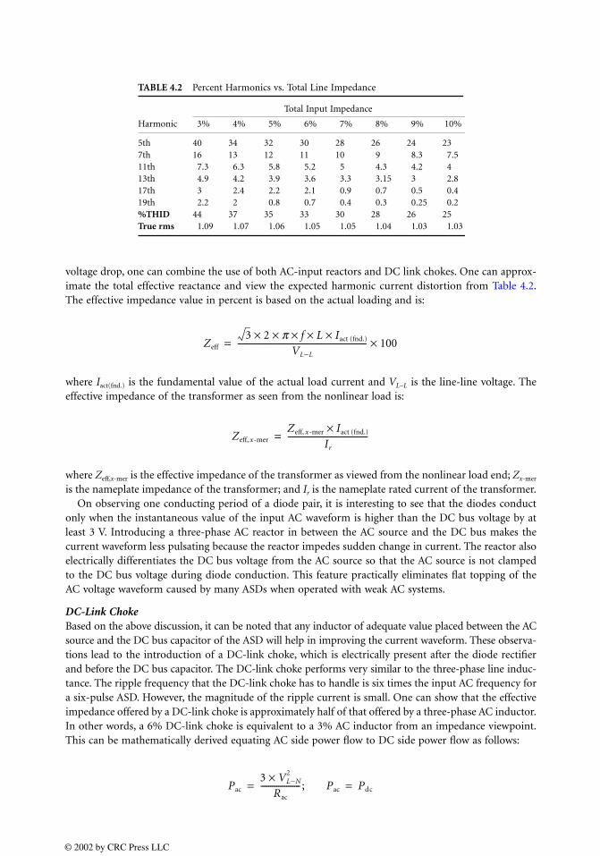
voltage drop, one can combine the use of both AC-input reactors and DC link chokes. One can approx-imate the total effective reactance and view the expected harmonic current distortion from Table 4.2.The effective impedance value in percent is based on the actual loading and is:
where Iact(fnd.) is the fundamental value of the actual load current and VL−L is the line-line voltage. Theeffective impedance of the transformer as seen from the nonlinear load is:
where Zeff,x-mer is the effective impedance of the transformer as viewed from the nonlinear load end; Zx-mer
is the nameplate impedance of the transformer; and Ir is the nameplate rated current of the transformer.On observing one conducting period of a diode pair, it is interesting to see that the diodes conduct
only when the instantaneous value of the input AC waveform is higher than the DC bus voltage by atleast 3 V. Introducing a three-phase AC reactor in between the AC source and the DC bus makes thecurrent waveform less pulsating because the reactor impedes sudden change in current. The reactor alsoelectrically differentiates the DC bus voltage from the AC source so that the AC source is not clampedto the DC bus voltage during diode conduction. This feature practically eliminates flat topping of theAC voltage waveform caused by many ASDs when operated with weak AC systems.
DC-Link ChokeBased on the above discussion, it can be noted that any inductor of adequate value placed between the ACsource and the DC bus capacitor of the ASD will help in improving the current waveform. These observa-tions lead to the introduction of a DC-link choke, which is electrically present after the diode rectifierand before the DC bus capacitor. The DC-link choke performs very similar to the three-phase line induc-tance. The ripple frequency that the DC-link choke has to handle is six times the input AC frequency fora six-pulse ASD. However, the magnitude of the ripple current is small. One can show that the effectiveimpedance offered by a DC-link choke is approximately half of that offered by a three-phase AC inductor.In other words, a 6% DC-link choke is equivalent to a 3% AC inductor from an impedance viewpoint.This can be mathematically derived equating AC side power flow to DC side power flow as follows:
TABLE 4.2 Percent Harmonics vs. Total Line Impedance
Total Input Impedance
Harmonic 3% 4% 5% 6% 7% 8% 9% 10%
5th 40 34 32 30 28 26 24 237th 16 13 12 11 10 9 8.3 7.511th 7.3 6.3 5.8 5.2 5 4.3 4.2 413th 4.9 4.2 3.9 3.6 3.3 3.15 3 2.817th 3 2.4 2.2 2.1 0.9 0.7 0.5 0.419th 2.2 2 0.8 0.7 0.4 0.3 0.25 0.2%THID 44 37 35 33 30 28 26 25True rms 1.09 1.07 1.06 1.05 1.05 1.04 1.03 1.03
Zeff
3 2 π f L Iact (fnd.)×××××VL−L
----------------------------------------------------------------- 100×=
Zeff, x-mer
Zeff, x-mer Iact (fnd.)×Ir
----------------------------------------=
Pac
3 VL−N2×
Rac
-------------------- ; Pac Pdc= =
© 2002 by CRC Press LLC

VL−N is the line-neutral voltage at the input to the three-phase rectifier.
Since 9/π2 is approximately equal to 1, the ratio of DC impedance to AC impedance can be said to be
approximately 1:2. The DC link choke is less expensive and smaller than a three-phase line reactor andis often included inside an ASD. However, as the derivation shows, one has to keep in mind that theeffective impedance offered by a DC link choke is only half its numerical impedance value when referredto the AC side. DC link chokes are electrically after the diode bridge and so they do not offer any significantspike or overvoltage surge protection to the diode bridge rectifiers. It is a good engineering practice toincorporate both a DC link choke and a three-phase line reactor in an ASD for better overall performance.
Passive FiltersPassive filters consist of passive components like inductors, capacitors, and resistors arranged in a pre-determined fashion either to attenuate the flow of harmonic components through them or to shunt theharmonic component into them. Passive filters can be of many types. Some popular ones are seriespassive filters, shunt passive filters, and low-pass broadband passive filters. Series and shunt passive filtersare effective only in the narrow proximity of the frequency at which they are tuned. Low-pass broadbandpassive filters have a broader bandwidth and attenuate almost all harmonics above their cutoff frequency.However, applying passive filters requires good knowledge of the power system because passive filtercomponents can interact with existing transformers and power factor correcting capacitors and couldcreate electrical instability by introducing resonance into the system. Some forms of low-pass broadbandpassive filters do not contribute to resonance but they are bulky, expensive, and occupy space. A typicallow-pass broadband filter structure popularly employed by users of ASDs is shown in Fig. 4.17.
Phase MultiplicationAs discussed previously, the characteristic harmonics generated by a full-wave rectifier bridge converteris a function of the pulse number for that converter. A 12-pulse converter will have the lowest harmonicorder of 11. In other words, the 5th, and the 7th harmonic orders are theoretically nonexistent in a 12-pulseconverter. Similarly, an 18-pulse converter will have harmonic spectrum starting from the 17th harmonicand upwards. The lowest harmonic order in a 24-pulse converter will be the 23rd. The size of the passiveharmonic filter needed to filter out the harmonics reduces as the order of the lowest harmonic in the currentspectrum increases. Hence, the size of the filter needed to filter the harmonics out of a 12-pulse converteris much smaller than that needed to filter out the harmonics of a 6-pulse converter. However, a 12-pulse
FIGURE 4.17 Schematic representation of a low-pass broadband harmonic filter connected to an ASD with dioderectifier front end. (U.S. Patent 5,444,609.)
Pdc
Vdc2
Rdc
------- ; Vdc
3 3 2× VL N–××π
------------------------------------------------ Hence, Rdc; 29
π2-----
Rac= = =
© 2002 by CRC Press LLC
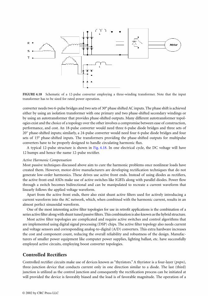
converter needs two 6-pulse bridges and two sets of 30° phase shifted AC inputs. The phase shift is achievedeither by using an isolation transformer with one primary and two phase-shifted secondary windings orby using an autotransformer that provides phase-shifted outputs. Many different autotransformer topol-ogies exist and the choice of a topology over the other involves a compromise between ease of construction,performance, and cost. An 18-pulse converter would need three 6-pulse diode bridges and three sets of20° phase-shifted inputs; similarly, a 24-pulse converter would need four 6-pulse diode bridges and foursets of 15° phase-shifted inputs. The transformers providing the phase-shifted outputs for multipulseconverters have to be properly designed to handle circulating harmonic flux.
A typical 12-pulse structure is shown in Fig. 4.18. In one electrical cycle, the DC voltage will have12 humps and hence the name 12-pulse rectifier.
Active Harmonic CompensationMost passive techniques discussed above aim to cure the harmonic problems once nonlinear loads havecreated them. However, motor-drive manufacturers are developing rectification techniques that do notgenerate low-order harmonics. These drives use active front ends. Instead of using diodes as rectifiers,the active front-end ASDs make use of active switches like IGBTs along with parallel diodes. Power flowthrough a switch becomes bidirectional and can be manipulated to recreate a current waveform thatlinearly follows the applied voltage waveform.
Apart from the active front ends, there also exist shunt active filters used for actively introducing acurrent waveform into the AC network, which, when combined with the harmonic current, results in analmost perfect sinusoidal waveform.
One of the most interesting active filter topologies for use in retrofit applications is the combination of aseries active filter along with shunt tuned passive filters. This combination is also known as the hybrid structure.
Most active filter topologies are complicated and require active switches and control algorithms thatare implemented using digital signal processing (DSP) chips. The active filter topology also needs currentand voltage sensors and corresponding analog-to-digital (A/D) converters. This extra hardware increasesthe cost and component count, reducing the overall reliability and robustness of the design. Manufac-turers of smaller power equipment like computer power supplies, lighting ballast, etc. have successfullyemployed active circuits, employing boost converter topologies.
Controlled Rectifiers
Controlled rectifier circuits make use of devices known as “thyristors.” A thyristor is a four-layer (pnpn),three-junction device that conducts current only in one direction similar to a diode. The last (third)junction is utilized as the control junction and consequently the rectification process can be initiated atwill provided the device is favorably biased and the load is of favorable magnitude. The operation of a
FIGURE 4.18 Schematic of a 12-pulse converter employing a three-winding transformer. Note that the inputtransformer has to be sized for rated power operation.
© 2002 by CRC Press LLC

thyristor can be explained by assuming it to be made up of two transistors connected back-to-back asshown in Fig. 4.19.
Let α1 and α2 be the ratio of collector to emitter currents of transistors Q1 and Q2, respectively. Inother words:
Also, from Fig. 4.19: Ie1 = Ie2 = IA where IA is the anode current flowing through the thyristor. Fromtransistor theory, the value of Ie2 is equal to Ic2 + Ib2 + Ilkg ; where Ilkg is the leakage current crossing then1 = p2-junction. From Fig. 4.19, Ib2 = Ic1 . Hence, the anode current can be rewritten as:
Substituting the collector currents by the product of ratio α and emitter current, the anode currentbecomes:
If the ratios of the collector current to base current (gain) of the transistors are assumed to be β1 andβ2, respectively, then the relationship between to β1 , β2 and α1 , α2 can be written as:
Substituting for α1 and α2 in the expression for IA yields the following expression:
If the values of α1 and α2 are low (low gains), then the anode current is low and comparable to theleakage current. Under this condition, the thyristor is said to be in its OFF state. However, if the effective
FIGURE 4.19 Virtual representation of a thyristor to explain its operation.
α1
Ic1
Ie1
----- ; α2
Ic2
Ie2
----- ;= =
IA Ic1 Ic2 Ilkg+ +=
IA α1 Ie1×( ) α2 Ie2×( ) Ilkg+ +=IA α1 α2+( )IA Ilkg+=
IA
Ilkg
1 α1 α2+( )–-------------------------------=
α1
β1
1 β1+-------------- ; α2
β2
1 β2+--------------==
IA
1 β1+( ) 1 β2+( )Ilkg
1 β1β2–--------------------------------------------- .=
© 2002 by CRC Press LLC
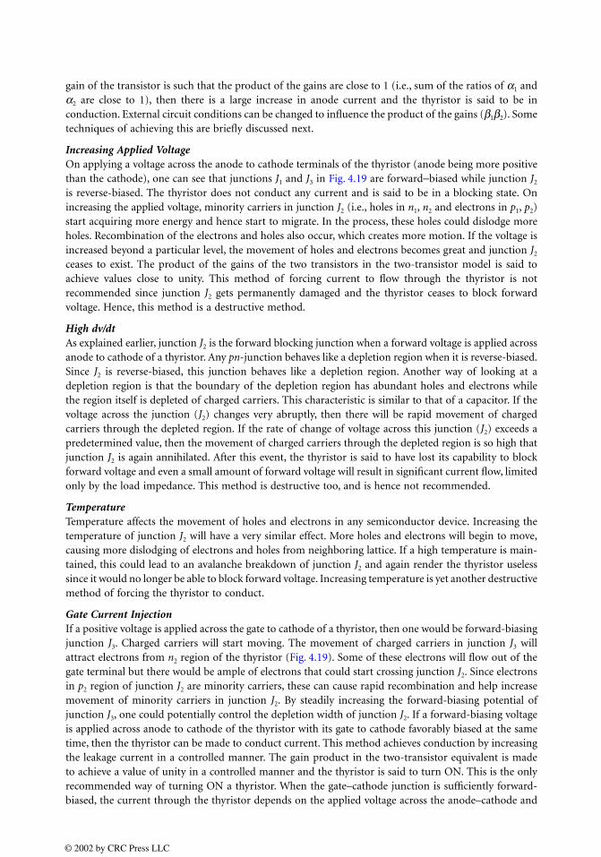
gain of the transistor is such that the product of the gains are close to 1 (i.e., sum of the ratios of α1 andα2 are close to 1), then there is a large increase in anode current and the thyristor is said to be inconduction. External circuit conditions can be changed to influence the product of the gains (β1β2). Sometechniques of achieving this are briefly discussed next.
Increasing Applied VoltageOn applying a voltage across the anode to cathode terminals of the thyristor (anode being more positivethan the cathode), one can see that junctions J1 and J3 in Fig. 4.19 are forward−biased while junction J2
is reverse-biased. The thyristor does not conduct any current and is said to be in a blocking state. Onincreasing the applied voltage, minority carriers in junction J2 (i.e., holes in n1, n2 and electrons in p1, p2)start acquiring more energy and hence start to migrate. In the process, these holes could dislodge moreholes. Recombination of the electrons and holes also occur, which creates more motion. If the voltage isincreased beyond a particular level, the movement of holes and electrons becomes great and junction J2
ceases to exist. The product of the gains of the two transistors in the two-transistor model is said toachieve values close to unity. This method of forcing current to flow through the thyristor is notrecommended since junction J2 gets permanently damaged and the thyristor ceases to block forwardvoltage. Hence, this method is a destructive method.
High dv/dtAs explained earlier, junction J2 is the forward blocking junction when a forward voltage is applied acrossanode to cathode of a thyristor. Any pn-junction behaves like a depletion region when it is reverse-biased.Since J2 is reverse-biased, this junction behaves like a depletion region. Another way of looking at adepletion region is that the boundary of the depletion region has abundant holes and electrons whilethe region itself is depleted of charged carriers. This characteristic is similar to that of a capacitor. If thevoltage across the junction (J2) changes very abruptly, then there will be rapid movement of chargedcarriers through the depleted region. If the rate of change of voltage across this junction (J2) exceeds apredetermined value, then the movement of charged carriers through the depleted region is so high thatjunction J2 is again annihilated. After this event, the thyristor is said to have lost its capability to blockforward voltage and even a small amount of forward voltage will result in significant current flow, limitedonly by the load impedance. This method is destructive too, and is hence not recommended.
TemperatureTemperature affects the movement of holes and electrons in any semiconductor device. Increasing thetemperature of junction J2 will have a very similar effect. More holes and electrons will begin to move,causing more dislodging of electrons and holes from neighboring lattice. If a high temperature is main-tained, this could lead to an avalanche breakdown of junction J2 and again render the thyristor uselesssince it would no longer be able to block forward voltage. Increasing temperature is yet another destructivemethod of forcing the thyristor to conduct.
Gate Current InjectionIf a positive voltage is applied across the gate to cathode of a thyristor, then one would be forward-biasingjunction J3. Charged carriers will start moving. The movement of charged carriers in junction J3 willattract electrons from n2 region of the thyristor (Fig. 4.19). Some of these electrons will flow out of thegate terminal but there would be ample of electrons that could start crossing junction J2. Since electronsin p2 region of junction J2 are minority carriers, these can cause rapid recombination and help increasemovement of minority carriers in junction J2. By steadily increasing the forward-biasing potential ofjunction J3, one could potentially control the depletion width of junction J2. If a forward-biasing voltageis applied across anode to cathode of the thyristor with its gate to cathode favorably biased at the sametime, then the thyristor can be made to conduct current. This method achieves conduction by increasingthe leakage current in a controlled manner. The gain product in the two-transistor equivalent is madeto achieve a value of unity in a controlled manner and the thyristor is said to turn ON. This is the onlyrecommended way of turning ON a thyristor. When the gate–cathode junction is sufficiently forward-biased, the current through the thyristor depends on the applied voltage across the anode–cathode and
© 2002 by CRC Press LLC
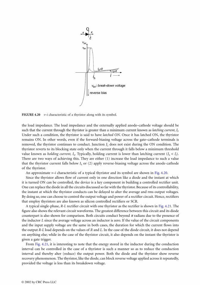
the load impedance. The load impedance and the externally applied anode–cathode voltage should besuch that the current through the thyristor is greater than a minimum current known as latching current, Il.Under such a condition, the thyristor is said to have latched ON. Once it has latched ON, the thyristorremains ON. In other words, even if the forward-biasing voltage across the gate–cathode terminals isremoved, the thyristor continues to conduct. Junction J2 does not exist during the ON condition. Thethyristor reverts to its blocking state only when the current through it falls below a minimum thresholdvalue known as holding current, Ih. Typically, holding current is lower than latching current (Ih < Il).There are two ways of achieving this. They are either (1) increase the load impedance to such a valuethat the thyristor current falls below Ih or (2) apply reverse-biasing voltage across the anode-cathodeof the thyristor.
An approximate v–i characteristic of a typical thyristor and its symbol are shown in Fig. 4.20.Since the thyristor allows flow of current only in one direction like a diode and the instant at which
it is turned ON can be controlled, the device is a key component in building a controlled rectifier unit.One can replace the diode in all the circuits discussed so far with the thyristor. Because of its controllability,the instant at which the thyristor conducts can be delayed to alter the average and rms output voltages.By doing so, one can choose to control the output voltage and power of a rectifier circuit. Hence, rectifiersthat employ thyristors are also known as silicon controlled rectifiers or SCR.
A typical single-phase, R-L rectifier circuit with one thyristor as the rectifier is shown in Fig. 4.21. Thefigure also shows the relevant circuit waveforms. The greatest difference between this circuit and its diodecounterpart is also shown for comparison. Both circuits conduct beyond π radians due to the presence ofthe inductor L since the average voltage across an inductor is zero. If the value of the circuit componentsand the input supply voltage are the same in both cases, the duration for which the current flows intothe output R-L load depends on the values of R and L. In the case of the diode circuit, it does not dependon anything else; while in the case of the thyristor circuit, it also depends on the instant the thyristor isgiven a gate trigger.
From Fig. 4.21, it is interesting to note that the energy stored in the inductor during the conductioninterval can be controlled in the case of a thyristor is such a manner so as to reduce the conductioninterval and thereby alter (reduce) the output power. Both the diode and the thyristor show reverserecovery phenomenon. The thyristor, like the diode, can block reverse voltage applied across it repeatedly,provided the voltage is less than its breakdown voltage.
FIGURE 4.20 v–i characteristic of a thyristor along with its symbol.
© 2002 by CRC Press LLC
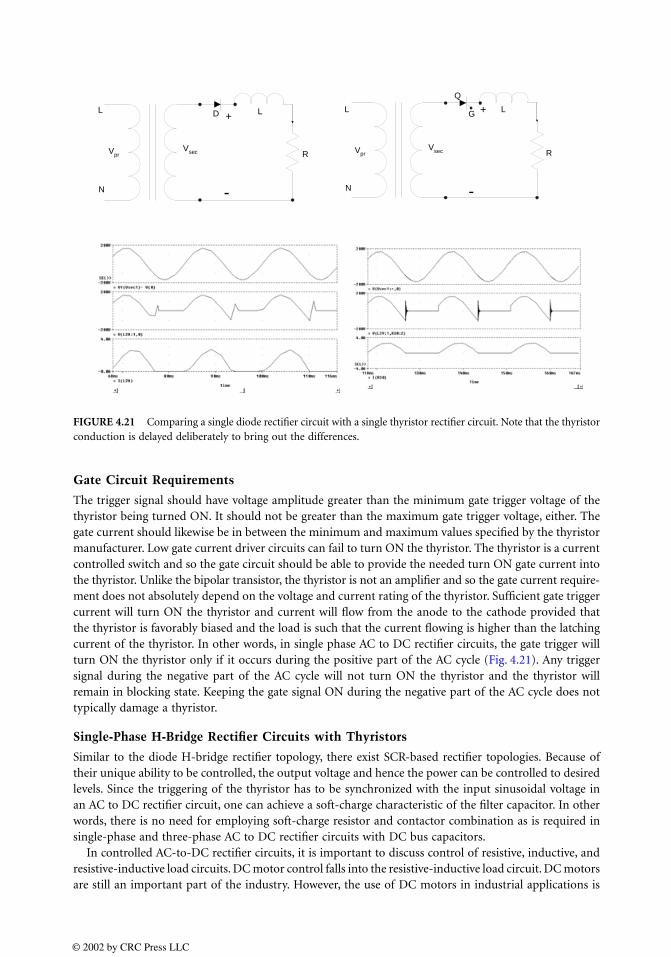
Gate Circuit Requirements
The trigger signal should have voltage amplitude greater than the minimum gate trigger voltage of thethyristor being turned ON. It should not be greater than the maximum gate trigger voltage, either. Thegate current should likewise be in between the minimum and maximum values specified by the thyristormanufacturer. Low gate current driver circuits can fail to turn ON the thyristor. The thyristor is a currentcontrolled switch and so the gate circuit should be able to provide the needed turn ON gate current intothe thyristor. Unlike the bipolar transistor, the thyristor is not an amplifier and so the gate current require-ment does not absolutely depend on the voltage and current rating of the thyristor. Sufficient gate triggercurrent will turn ON the thyristor and current will flow from the anode to the cathode provided thatthe thyristor is favorably biased and the load is such that the current flowing is higher than the latchingcurrent of the thyristor. In other words, in single phase AC to DC rectifier circuits, the gate trigger willturn ON the thyristor only if it occurs during the positive part of the AC cycle (Fig. 4.21). Any triggersignal during the negative part of the AC cycle will not turn ON the thyristor and the thyristor willremain in blocking state. Keeping the gate signal ON during the negative part of the AC cycle does nottypically damage a thyristor.
Single-Phase H-Bridge Rectifier Circuits with Thyristors
Similar to the diode H-bridge rectifier topology, there exist SCR-based rectifier topologies. Because oftheir unique ability to be controlled, the output voltage and hence the power can be controlled to desiredlevels. Since the triggering of the thyristor has to be synchronized with the input sinusoidal voltage inan AC to DC rectifier circuit, one can achieve a soft-charge characteristic of the filter capacitor. In otherwords, there is no need for employing soft-charge resistor and contactor combination as is required insingle-phase and three-phase AC to DC rectifier circuits with DC bus capacitors.
In controlled AC-to-DC rectifier circuits, it is important to discuss control of resistive, inductive, andresistive-inductive load circuits. DC motor control falls into the resistive-inductive load circuit. DC motorsare still an important part of the industry. However, the use of DC motors in industrial applications is
FIGURE 4.21 Comparing a single diode rectifier circuit with a single thyristor rectifier circuit. Note that the thyristorconduction is delayed deliberately to bring out the differences.
L
N
D
VprVsec
+
-
R
L L
N
Q
VprVsec
+
-
R
G L
© 2002 by CRC Press LLC
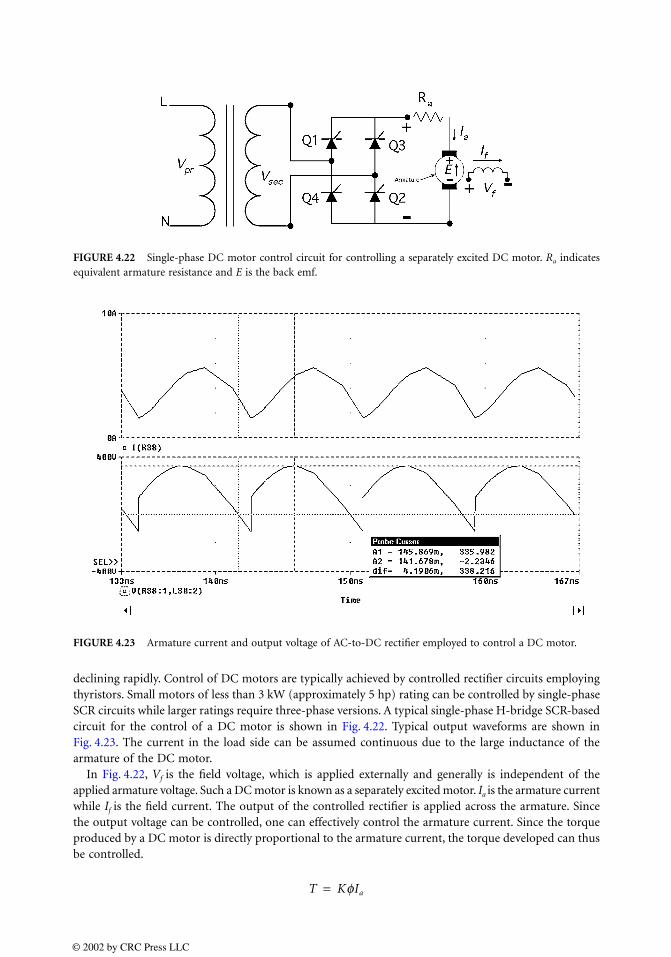
declining rapidly. Control of DC motors are typically achieved by controlled rectifier circuits employingthyristors. Small motors of less than 3 kW (approximately 5 hp) rating can be controlled by single-phaseSCR circuits while larger ratings require three-phase versions. A typical single-phase H-bridge SCR-basedcircuit for the control of a DC motor is shown in Fig. 4.22. Typical output waveforms are shown inFig. 4.23. The current in the load side can be assumed continuous due to the large inductance of thearmature of the DC motor.
In Fig. 4.22, Vf is the field voltage, which is applied externally and generally is independent of theapplied armature voltage. Such a DC motor is known as a separately excited motor. Ia is the armature currentwhile If is the field current. The output of the controlled rectifier is applied across the armature. Sincethe output voltage can be controlled, one can effectively control the armature current. Since the torqueproduced by a DC motor is directly proportional to the armature current, the torque developed can thusbe controlled.
FIGURE 4.22 Single-phase DC motor control circuit for controlling a separately excited DC motor. Ra indicatesequivalent armature resistance and E is the back emf.
FIGURE 4.23 Armature current and output voltage of AC-to-DC rectifier employed to control a DC motor.
T KφIa=
© 2002 by CRC Press LLC
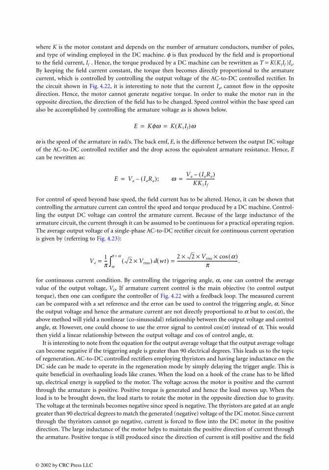
where K is the motor constant and depends on the number of armature conductors, number of poles,and type of winding employed in the DC machine. φ is flux produced by the field and is proportionalto the field current, If . Hence, the torque produced by a DC machine can be rewritten as T = K(K1If )Ia.By keeping the field current constant, the torque then becomes directly proportional to the armaturecurrent, which is controlled by controlling the output voltage of the AC-to-DC controlled rectifier. Inthe circuit shown in Fig. 4.22, it is interesting to note that the current Ia, cannot flow in the oppositedirection. Hence, the motor cannot generate negative torque. In order to make the motor run in theopposite direction, the direction of the field has to be changed. Speed control within the base speed canalso be accomplished by controlling the armature voltage as is shown below.
ω is the speed of the armature in rad/s. The back emf, E, is the difference between the output DC voltageof the AC-to-DC controlled rectifier and the drop across the equivalent armature resistance. Hence, Ecan be rewritten as:
For control of speed beyond base speed, the field current has to be altered. Hence, it can be shown thatcontrolling the armature current can control the speed and torque produced by a DC machine. Control-ling the output DC voltage can control the armature current. Because of the large inductance of thearmature circuit, the current through it can be assumed to be continuous for a practical operating region.The average output voltage of a single-phase AC-to-DC rectifier circuit for continuous current operationis given by (referring to Fig. 4.23):
for continuous current condition. By controlling the triggering angle, α, one can control the averagevalue of the output voltage, VO. If armature current control is the main objective (to control outputtorque), then one can configure the controller of Fig. 4.22 with a feedback loop. The measured currentcan be compared with a set reference and the error can be used to control the triggering angle, α. Sincethe output voltage and hence the armature current are not directly proportional to α but to cos(α), theabove method will yield a nonlinear (co-sinusoidal) relationship between the output voltage and controlangle, α. However, one could choose to use the error signal to control cos(α) instead of α. This wouldthen yield a linear relationship between the output voltage and cos of control angle, α.
It is interesting to note from the equation for the output average voltage that the output average voltagecan become negative if the triggering angle is greater than 90 electrical degrees. This leads us to the topicof regeneration. AC-to-DC controlled rectifiers employing thyristors and having large inductance on theDC side can be made to operate in the regeneration mode by simply delaying the trigger angle. This isquite beneficial in overhauling loads like cranes. When the load on a hook of the crane has to be liftedup, electrical energy is supplied to the motor. The voltage across the motor is positive and the currentthrough the armature is positive. Positive torque is generated and hence the load moves up. When theload is to be brought down, the load starts to rotate the motor in the opposite direction due to gravity.The voltage at the terminals becomes negative since speed is negative. The thyristors are gated at an anglegreater than 90 electrical degrees to match the generated (negative) voltage of the DC motor. Since currentthrough the thyristors cannot go negative, current is forced to flow into the DC motor in the positivedirection. The large inductance of the motor helps to maintain the positive direction of current throughthe armature. Positive torque is still produced since the direction of current is still positive and the field
E Kφω K K1If( )ω= =
E Va IaRa( ); ω–Va IaRa( )–
KK1If
--------------------------= =
Vo1π--- 2 Vrms×( ) wt( )d
α
π α+
∫2 2× Vrms α( )cos××
π--------------------------------------------------------= = .
© 2002 by CRC Press LLC
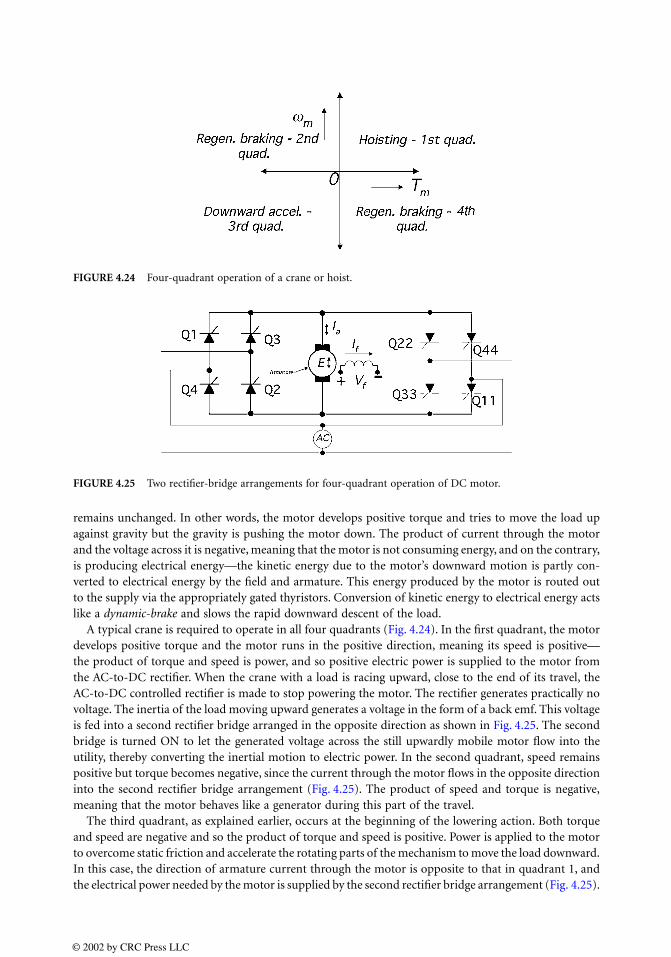
remains unchanged. In other words, the motor develops positive torque and tries to move the load upagainst gravity but the gravity is pushing the motor down. The product of current through the motorand the voltage across it is negative, meaning that the motor is not consuming energy, and on the contrary,is producing electrical energy—the kinetic energy due to the motor’s downward motion is partly con-verted to electrical energy by the field and armature. This energy produced by the motor is routed outto the supply via the appropriately gated thyristors. Conversion of kinetic energy to electrical energy actslike a dynamic-brake and slows the rapid downward descent of the load.
A typical crane is required to operate in all four quadrants (Fig. 4.24). In the first quadrant, the motordevelops positive torque and the motor runs in the positive direction, meaning its speed is positive—the product of torque and speed is power, and so positive electric power is supplied to the motor fromthe AC-to-DC rectifier. When the crane with a load is racing upward, close to the end of its travel, theAC-to-DC controlled rectifier is made to stop powering the motor. The rectifier generates practically novoltage. The inertia of the load moving upward generates a voltage in the form of a back emf. This voltageis fed into a second rectifier bridge arranged in the opposite direction as shown in Fig. 4.25. The secondbridge is turned ON to let the generated voltage across the still upwardly mobile motor flow into theutility, thereby converting the inertial motion to electric power. In the second quadrant, speed remainspositive but torque becomes negative, since the current through the motor flows in the opposite directioninto the second rectifier bridge arrangement (Fig. 4.25). The product of speed and torque is negative,meaning that the motor behaves like a generator during this part of the travel.
The third quadrant, as explained earlier, occurs at the beginning of the lowering action. Both torqueand speed are negative and so the product of torque and speed is positive. Power is applied to the motorto overcome static friction and accelerate the rotating parts of the mechanism to move the load downward.In this case, the direction of armature current through the motor is opposite to that in quadrant 1, andthe electrical power needed by the motor is supplied by the second rectifier bridge arrangement (Fig. 4.25).
FIGURE 4.24 Four-quadrant operation of a crane or hoist.
FIGURE 4.25 Two rectifier-bridge arrangements for four-quadrant operation of DC motor.
© 2002 by CRC Press LLC

The mechanical load and motor arrangement goes into the fourth quadrant of operation for the largerpart of the downward motion. This is the period during which the motor resists the tendency of the loadto accelerate downward by developing positive torque. Since motion is downward, speed is negativeand the product of torque and speed is negative. This means the motor behaves like a generator as explainedearlier.
Since the thyristors cannot conduct in the opposite direction, a new inverter section had to be providedto enable the four-quadrant operation needed in cranes and hoists. The method by which unidirectionalelectrical power was routed to the bidirectional AC utility lines is known as inversion (opposite ofrectification). Since no external means of switching OFF the thyristors was employed, the process ofinversion was achieved by natural commutation. Such an inverter is also known as a line commutatedinverter.
Three-Phase Controlled AC-to-DC Rectifier Systems
The observations made so far for the single-phase controlled AC-to-DC rectifiers can be easily extendedto three-phase versions. An important controlled rectification scheme that was not mentioned in thesingle-phase case is the semiconverter circuit. In Fig. 4.22, if the thyristors Q2 and Q4 are replaced bydiodes (D2 and D4), then the circuit of Fig. 4.22 is converted into a semiconverter circuit. Such a circuit doesnot have the potential to provide regeneration capability and hence is of limited use. However, in dualconverter applications, especially in three-phase versions, there are a few instances where a semiconvertercan be employed to reduce cost. A typical three-phase semiconverter circuit will consist of three thyristorsand three diodes arranged in an H-bridge configuration as shown in Fig. 4.26.
Three-phase dual converter schemes similar to the one shown in Fig. 4.25 are still employed to operatelarge steel mills, hoists, and cranes. However, the advent of vector-controlled AC drives has drasticallychanged the electrical landscape of the modern industry. Most DC motor applications are being rapidlyreplaced by AC motors with field-oriented control schemes. DC motor application in railway tractionhas also seen significant reduction due to the less expensive and more robust AC motors.
However, there are still a few important applications where three-phase controlled rectification (inver-sion) is the most cost-effective solution. One such application is the regenerative converter module thatmany inverter-drive manufacturers provide as optional equipment to customers with overhauling loads.Under normal circumstances, during the motoring mode of operation of an AC drive, the regenerativeunit does not come into the circuit. However, when the DC bus voltage tends to go higher than apredetermined level due to overhauling of the load, the kinetic energy of the load is converted intoelectrical energy and is fed back into the AC system via a six-pulse thyristor-based inverter-bridge. Onesuch scheme is shown in Fig. 4.27.
FIGURE 4.26 A typical three-phase semiconverter. Rarely employed in modern industry.
© 2002 by CRC Press LLC
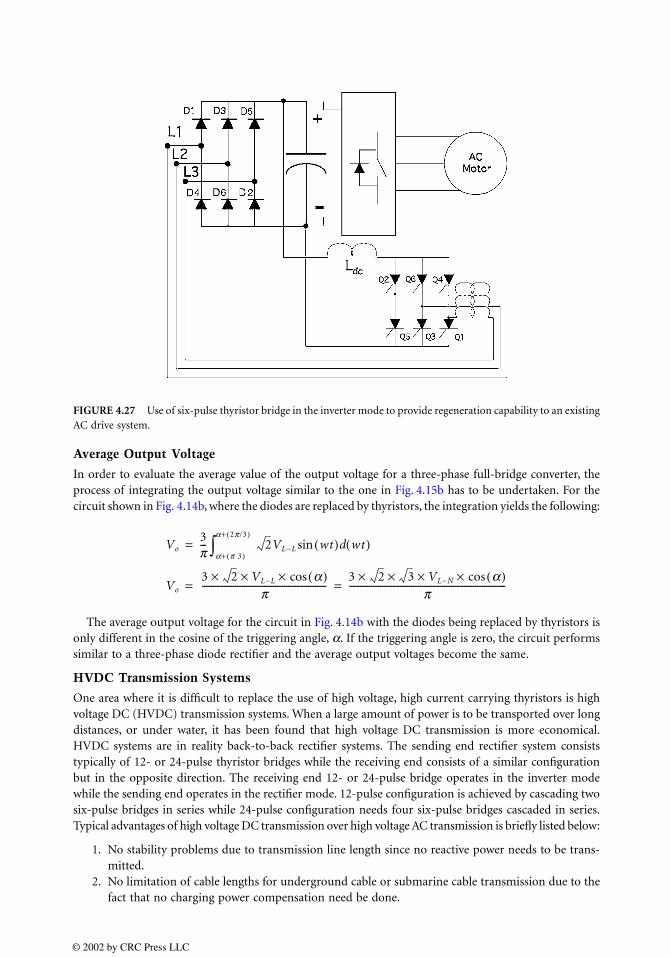
Average Output Voltage
In order to evaluate the average value of the output voltage for a three-phase full-bridge converter, theprocess of integrating the output voltage similar to the one in Fig. 4.15b has to be undertaken. For thecircuit shown in Fig. 4.14b, where the diodes are replaced by thyristors, the integration yields the following:
The average output voltage for the circuit in Fig. 4.14b with the diodes being replaced by thyristors isonly different in the cosine of the triggering angle, α. If the triggering angle is zero, the circuit performssimilar to a three-phase diode rectifier and the average output voltages become the same.
HVDC Transmission Systems
One area where it is difficult to replace the use of high voltage, high current carrying thyristors is highvoltage DC (HVDC) transmission systems. When a large amount of power is to be transported over longdistances, or under water, it has been found that high voltage DC transmission is more economical.HVDC systems are in reality back-to-back rectifier systems. The sending end rectifier system consiststypically of 12- or 24-pulse thyristor bridges while the receiving end consists of a similar configurationbut in the opposite direction. The receiving end 12- or 24-pulse bridge operates in the inverter modewhile the sending end operates in the rectifier mode. 12-pulse configuration is achieved by cascading twosix-pulse bridges in series while 24-pulse configuration needs four six-pulse bridges cascaded in series.Typical advantages of high voltage DC transmission over high voltage AC transmission is briefly listed below:
1. No stability problems due to transmission line length since no reactive power needs to be trans-mitted.
2. No limitation of cable lengths for underground cable or submarine cable transmission due to thefact that no charging power compensation need be done.
FIGURE 4.27 Use of six-pulse thyristor bridge in the inverter mode to provide regeneration capability to an existingAC drive system.
Vo3π--- 2VL−L wt( ) wt( )dsin
α+ π 3( )
α+ 2π/3( )
∫=
Vo
3 2× VL−L α( )cos××π
--------------------------------------------------------3 2× 3 VL−N α( )cos×××
π-----------------------------------------------------------------------= =
© 2002 by CRC Press LLC
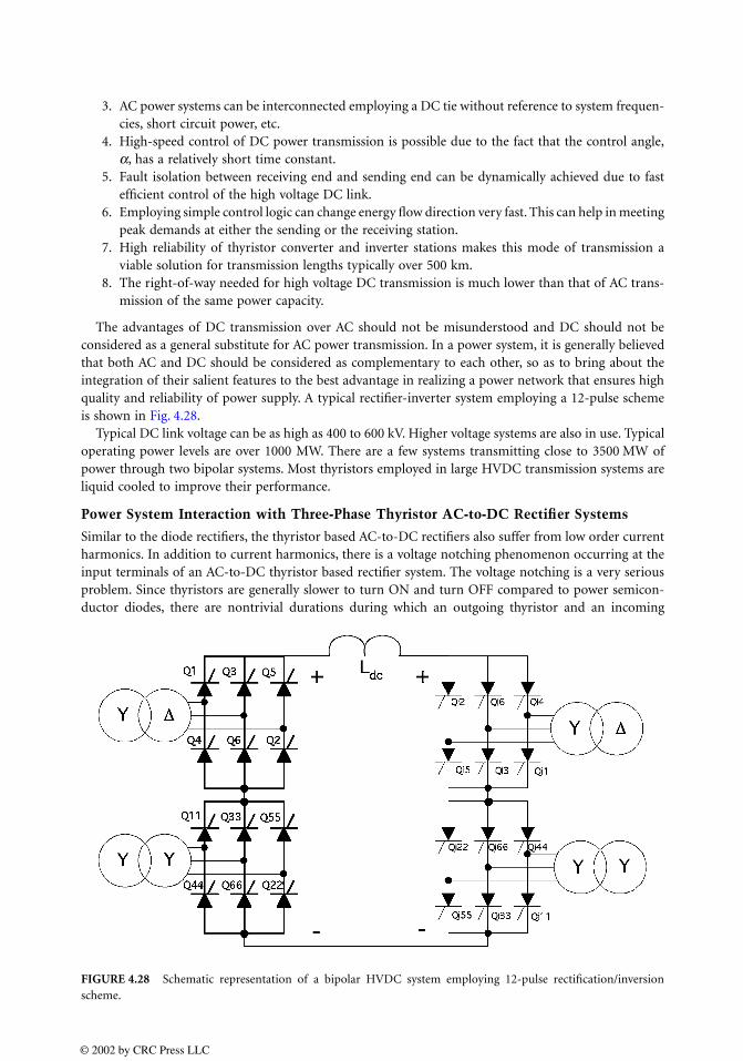
3. AC power systems can be interconnected employing a DC tie without reference to system frequen-cies, short circuit power, etc.
4. High-speed control of DC power transmission is possible due to the fact that the control angle,α, has a relatively short time constant.
5. Fault isolation between receiving end and sending end can be dynamically achieved due to fastefficient control of the high voltage DC link.
6. Employing simple control logic can change energy flow direction very fast. This can help in meetingpeak demands at either the sending or the receiving station.
7. High reliability of thyristor converter and inverter stations makes this mode of transmission aviable solution for transmission lengths typically over 500 km.
8. The right-of-way needed for high voltage DC transmission is much lower than that of AC trans-mission of the same power capacity.
The advantages of DC transmission over AC should not be misunderstood and DC should not beconsidered as a general substitute for AC power transmission. In a power system, it is generally believedthat both AC and DC should be considered as complementary to each other, so as to bring about theintegration of their salient features to the best advantage in realizing a power network that ensures highquality and reliability of power supply. A typical rectifier-inverter system employing a 12-pulse schemeis shown in Fig. 4.28.
Typical DC link voltage can be as high as 400 to 600 kV. Higher voltage systems are also in use. Typicaloperating power levels are over 1000 MW. There are a few systems transmitting close to 3500 MW ofpower through two bipolar systems. Most thyristors employed in large HVDC transmission systems areliquid cooled to improve their performance.
Power System Interaction with Three-Phase Thyristor AC-to-DC Rectifier Systems
Similar to the diode rectifiers, the thyristor based AC-to-DC rectifiers also suffer from low order currentharmonics. In addition to current harmonics, there is a voltage notching phenomenon occurring at theinput terminals of an AC-to-DC thyristor based rectifier system. The voltage notching is a very seriousproblem. Since thyristors are generally slower to turn ON and turn OFF compared to power semicon-ductor diodes, there are nontrivial durations during which an outgoing thyristor and an incoming
FIGURE 4.28 Schematic representation of a bipolar HVDC system employing 12-pulse rectification/inversionscheme.
© 2002 by CRC Press LLC
thyristor remain in conduction, thereby creating a short-circuit across the power supply phases feeding thecorresponding thyristors. Thyristors used in rectifiers are generally known as phase control type thyristorsand have typical turn OFF times of 50 to 100 µs. Thyristors employed in inverter circuits typically arefaster and have turn OFF times in the 10 to 50 µs range.
Notching can create major disturbances in sensitive electronic equipment that rely on the zero-crossingof the voltage for satisfactory operation. Multiple pseudo-zero-crossings of the voltage waveform can occurdue to the notching effect of thyristor-based rectifier systems. Notching can create large magnitudes ofcurrents to flow into power-factor correcting capacitors, thereby potentially causing permanent damageto them. IEEE Std. 519-1992 in the United States has strict regulations regarding the depth of the notchas well as the duration of the notch. AC line inductors in series with the supply feeding power to thethree-phase bridge help to minimize the notching effect on the power system. The theory behind thisphenomenon is discussed next.
When an external inductance is added in front of a three-phase AC-to-DC rectifier employing thyris-tors, the duration of commutation increases. In other words, the time period for which the outgoingthyristor remains in conduction along with the incoming thyristor increases. This overlap period causesthe average output voltage to reduce because during this period, the output voltage is composed of twoshorted phases and a healthy phase. The extent of reduction in the output voltage depends on the durationof overlap in electrical degrees. The duration of overlap in electrical degrees is commonly representedby µ. The overlap duration is directly proportional to the value of the external inductance used. If noexternal line inductor is used, then this duration will depend on the existing inductance of the systemincluding the wiring inductance. In order to compute the factors influencing the overlap duration, asimple model can be assumed. Assume that the line is comprised of inductance L in each phase. Let theDC load current be Idc and let it be assumed that this current does not change during the overlap interval.The current in the incoming thyristor is zero at start and by the end of the overlap interval, it rises toIdc. Based on this assumption, the relationship between current and voltage can be expressed as:
For small values of overlap angle µ, sin(µ/2) = µ/2 and sin(α + π/3 + (µ/2)) = sin(α + π/3). Rearrangingthe above equation yields:
From the above expression, it is interesting to note the following:
1. If the inductance L in the form of either external inductance or leakage inductance of transformeror lead length is large, the overlap duration will be large.
2. If the load current Idc is large, the overlap duration will be large.3. If the delay angle is small, then the inductance will store more energy and so the duration of
overlap will be large. The minimum value of delay angle α is 0° and the maximum value typicallyis 60°.
vab 2 VL−L wt( )sin×× 2 L di/dt( )××= =
2 VL−L wt( )sin t( )dα+ π/3( )
α+ π/3( ) µ+
∫×× 2 L id0
Idc
∫××=
Idc
2 VL−L α π/3+( )cos α π/3 µ++( )cos–( )××2wL
-------------------------------------------------------------------------------------------------------------------=
2 VL−L α π 3 µ/2++( )sin µ/2( )sin×××wL
--------------------------------------------------------------------------------------------------------=
µ2wL Idc×
2 VL−L α π 3⁄+( )sin××---------------------------------------------------------------=
© 2002 by CRC Press LLC
The average output voltage will reduce due to the overlap angle as mentioned before. In order tocompute the average output voltage with a certain overlap angle, the limits of integration have to bechanged. This exercise yields the following:
Thus, it can be seen that the overlap angle has an equivalent effect of advancing the delay angle, therebyreducing the average output voltage. From the discussions in the previous paragraphs on notching, it isinteresting to note that adding external inductance increases the duration of the overlap and reduces theaverage value of the output DC voltage. However, when viewed from the AC source side, the notchingeffect is conspicuously reduced and in some cases not observable. Since all other electrical equipment inthe system will be connected to the line side of the AC inductor (in front of a thyristor-based AC-to-DCrectifier), these equipment will not be affected by the notching phenomenon of thyristors. The externalinductance also helps limit the circulating current between the two thyristors during the overlap duration.
Conclusion
Uncontrolled and controlled rectifier circuits have been discussed in this section. An introduction to thetheory of diode and thyristor conduction has been presented to explain the important operating char-acteristics of these devices. Rectifier topologies employing both diodes and thyristors and their relativeadvantages and disadvantages have been discussed. Use of a dual thyristor bridge converter to achievefour-quadrant operation of a DC motor has been discussed. The topic of high-voltage DC (HVDC)transmission has been briefly introduced. Power quality issues relating to diode and thyristor-basedrectifier topologies has also been addressed. To probe further into the various topics briefly discussed inthis section, the reader is encouraged to refer to the references listed below.
References
Dewan, S. B. and Straughen, A., Power Semiconductor Circuits, John Wiley & Sons, New York, 1975.Hoft, R. G., Semiconductor Power Electronics, Van Nostrand Reinhold, New York, 1986.IEEE Recommended Practices and Requirements for Harmonic Control in Electrical Power Systems, IEEE
Std. 519–1992.Laughton M. A. and Say, M. G., Eds., Electrical Engineer’s Reference Book, 14th ed., Butterworths, Boston,
1985.Passive Harmonic Filter Systems for Variable Frequency Drives, U.S. Patent 5,444,609, 1995.Sen, P. C., Principles of Electric Machines and Power Electronics, John Wiley & Sons, New York, 1997.
4.3 Three-Phase Pulse-Width-Modulated Boost-Type Rectifiers
Ana Stankovic
Introduction
The boost-type rectifier has been extensively developed and analyzed in recent years [1, 3, 6]. It offersadvantages over traditionally used phase-controlled thyristor rectifiers in AC-DC-AC converters forvariable-control drives because of its capability for nearly instantaneous reversal of power flow, powerfactor management, and reduction of input harmonic distortion. Figure 4.29 shows the structure of thepulse-width-modulated (PWM) boost-type rectifier.
Vo3π--- 2VL L– wt( )sin wt( )d
α+µ+ π 3( )
α+µ+ 2π /3( )
∫=
Vo
3 2× VL−L α µ+( )cos××π
------------------------------------------------------------------3 2× 3 VL−N α µ+( )cos×××
π--------------------------------------------------------------------------------= =
© 2002 by CRC Press LLC
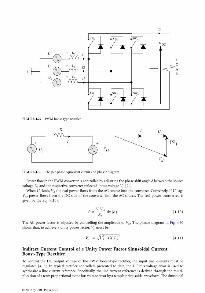
Power flow in the PWM converter is controlled by adjusting the phase shift angle δ between the sourcevoltage U1 and the respective converter reflected input voltage Vs1 [2].
When U1 leads Vs1 the real power flows from the AC source into the converter. Conversely, if U1 lagsVs1, power flows from the DC side of the converter into the AC source. The real power transferred isgiven by the Eq. (4.10).
(4.10)
The AC power factor is adjusted by controlling the amplitude of Vs1. The phasor diagram in Fig. 4.30shows that, to achieve a unity power factor, Vs1 must be
(4.11)
Indirect Current Control of a Unity Power Factor Sinusoidal CurrentBoost-Type Rectifier
To control the DC output voltage of the PWM boost-type rectifier, the input line currents must beregulated [4, 5]. In typical rectifier controllers presented to date, the DC bus voltage error is used tosynthesize a line current reference. Specifically, the line current reference is derived through the multi-plication of a term proportional to the bus voltage error by a template sinusoidal waveform. The sinusoidal
FIGURE 4.29 PWM boost-type rectifier.
FIGURE 4.30 The per-phase equivalent circuit and phasor diagram.
SW3
SW5
VDC
SW1 SW2
SW6SW4
+ L1
+ L1
+ L1
i1
i3
i2
U1
U3
U2
I0
LOAD
jX
I
U
+ +V
1
1
s1
Vs1
U1
jXI1
I1
PU1Vs1
X1
--------------= δ( )sin
Vs1 U12 X1I1( )2+=
© 2002 by CRC Press LLC
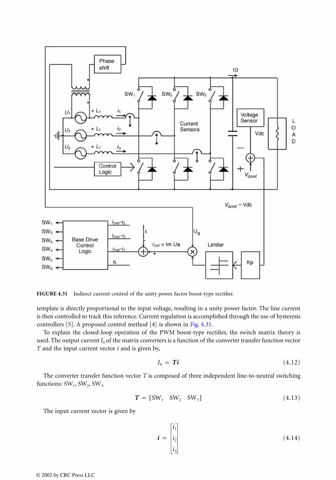
template is directly proportional to the input voltage, resulting in a unity power factor. The line currentis then controlled to track this reference. Current regulation is accomplished through the use of hysteresiscontrollers [5]. A proposed control method [4] is shown in Fig. 4.31.
To explain the closed-loop operation of the PWM boost-type rectifier, the switch matrix theory isused. The output current I0 of the matrix converters is a function of the converter transfer function vectorT and the input current vector i and is given by,
(4.12)
The converter transfer function vector T is composed of three independent line-to-neutral switchingfunctions: SW1, SW2, SW3.
(4.13)
The input current vector is given by
(4.14)
FIGURE 4.31 Indirect current control of the unity power factor boost-type rectifier.
I0 Ti=
T SW1 SW2 SW3[ ]=
i
i1
i2
i3
=
© 2002 by CRC Press LLC

The line-to-neutral switching functions are balanced and are represented by their fundamental com-ponents only.
(4.15)
Therefore, converter synthesized line-to-neutral voltages can be expressed as
(4.16)
Eq. (4.15) shows the rectifier synthesized voltages. Vdc represents the output DC voltage.In the time domain, the fundamental components of the three-phase input currents are given by
(4.17)
By combining Eqs. (4.12), (4.15), and (4.17), the output current I0(t) is obtained, given by
(4.18)
By using a trigonometric identity, I0(t) becomes
(4.19)
Because the angle (Θ − ϕ1) is constant for any set value of the input power factor, the output DCcurrent, I0(t), is proportional to the magnitude of the input current, I1(t), and so is the output voltage,Vdc. For unity power factor control, angle ϕ1 is equal to zero.
The output voltage, Vdc is
(4.20)
(4.21)
Figure 4.30 shows that the DC bus error, (Vdcref − Vdc), is used to set the reference for the input currentmagnitude. The input sinusoidal voltage, Ua, is multiplied by the DC bus error and it becomes a referencefor the input current in phase 1. The reference value for current in phase 2 is phase-shifted by 120° withrespect to the current in phase 1. Since the sum of three input currents is always zero, the reference forcurrent in phase 3 is obtained from the following equation:
(4.22)
SW1 t( ) S1 wt Θ–( )sin=SW2 t( ) S1 wt Θ– 120°–( )sin=SW3 t( ) S1 wt 120° Θ–+( )sin=
Vs112--VdcS1 wt Θ–( )sin=
Vs212--VdcS1 wt 120° Θ––( )sin=
Vs312--VdcS1 wt 120° Θ–+( )sin=
i1 t( ) I1 wt ϕ1–( )sin=i2 t( ) I1 wt 120°– ϕ1–( )sin=i3 t( ) I1 wt 120° ϕ1–+( )sin=
I0 t( ) I1 wt ϕ1–( )sin S1 wt Θ–( )sin I1 wt 120° ϕ– 1–( )S1sin wt 120° Θ––( )sin+=I1 wt 120° ϕ– 1+( )sin S1 wt 120° Θ–+( )sin+
I0 t( ) 32-- I1S1 Θ ϕ1–( )cos=
Vdc RI0=
Vdcref Vdc–( ) KI1=
i3ref t( ) −i1ref t( ) i2ref t( )–=
© 2002 by CRC Press LLC
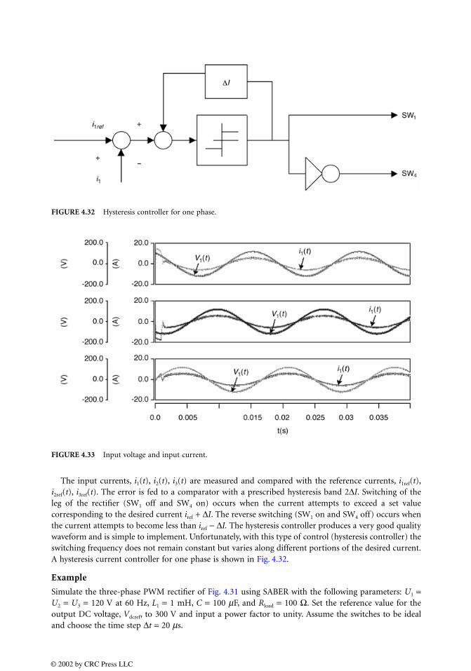
The input currents, i1(t), i2(t), i3(t) are measured and compared with the reference currents, i1ref(t),i2ref(t), i3ref(t). The error is fed to a comparator with a prescribed hysteresis band 2∆I. Switching of theleg of the rectifier (SW1 off and SW4 on) occurs when the current attempts to exceed a set valuecorresponding to the desired current iref + ∆I. The reverse switching (SW1 on and SW4 off) occurs whenthe current attempts to become less than iref − ∆I. The hysteresis controller produces a very good qualitywaveform and is simple to implement. Unfortunately, with this type of control (hysteresis controller) theswitching frequency does not remain constant but varies along different portions of the desired current.A hysteresis current controller for one phase is shown in Fig. 4.32.
Example
Simulate the three-phase PWM rectifier of Fig. 4.31 using SABER with the following parameters: U1 =U2 = U3 = 120 V at 60 Hz, L1 = 1 mH, C = 100 µF, and Rload = 100 Ω. Set the reference value for theoutput DC voltage, Vdcref, to 300 V and input a power factor to unity. Assume the switches to be idealand choose the time step ∆t = 20 µs.
FIGURE 4.32 Hysteresis controller for one phase.
FIGURE 4.33 Input voltage and input current.
© 2002 by CRC Press LLC
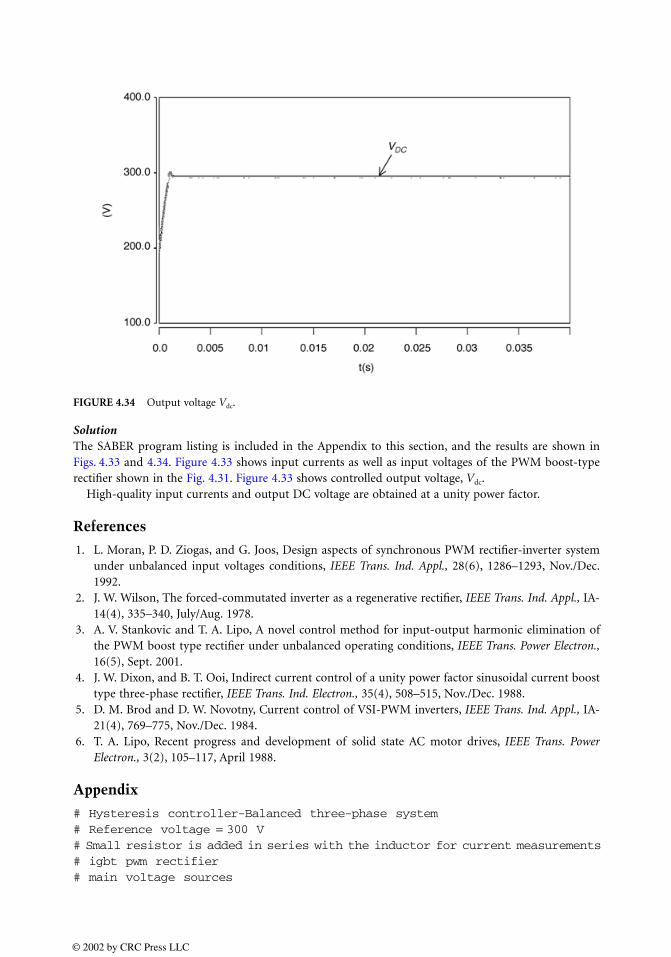
SolutionThe SABER program listing is included in the Appendix to this section, and the results are shown inFigs. 4.33 and 4.34. Figure 4.33 shows input currents as well as input voltages of the PWM boost-typerectifier shown in the Fig. 4.31. Figure 4.33 shows controlled output voltage, Vdc.
High-quality input currents and output DC voltage are obtained at a unity power factor.
References
1. L. Moran, P. D. Ziogas, and G. Joos, Design aspects of synchronous PWM rectifier-inverter systemunder unbalanced input voltages conditions, IEEE Trans. Ind. Appl., 28(6), 1286–1293, Nov./Dec.1992.
2. J. W. Wilson, The forced-commutated inverter as a regenerative rectifier, IEEE Trans. Ind. Appl., IA-14(4), 335–340, July/Aug. 1978.
3. A. V. Stankovic and T. A. Lipo, A novel control method for input-output harmonic elimination ofthe PWM boost type rectifier under unbalanced operating conditions, IEEE Trans. Power Electron.,16(5), Sept. 2001.
4. J. W. Dixon, and B. T. Ooi, Indirect current control of a unity power factor sinusoidal current boosttype three-phase rectifier, IEEE Trans. Ind. Electron., 35(4), 508–515, Nov./Dec. 1988.
5. D. M. Brod and D. W. Novotny, Current control of VSI-PWM inverters, IEEE Trans. Ind. Appl., IA-21(4), 769–775, Nov./Dec. 1984.
6. T. A. Lipo, Recent progress and development of solid state AC motor drives, IEEE Trans. PowerElectron., 3(2), 105–117, April 1988.
Appendix
# Hysteresis controller-Balanced three-phase system# Reference voltage = 300 V# Small resistor is added in series with the inductor for current measurements# igbt pwm rectifier # main voltage sources
FIGURE 4.34 Output voltage Vdc.
© 2002 by CRC Press LLC

# Program for balanced voltages and balanced impedances-Closed-loop solution# Hysteresis Controller + P-I controller
vac.va n11 n17 = va = 120, theta = 0, f = 60vac.vb n12 n17 = va = 120, theta = -120, f = 60vac.vc n13 n17 = va = 120, theta = 120, f = 60
r.111 n11 n111 = 0.001r.222 n12 n122 = 0.001r.333 n13 n133 = 0.001
v.vpl vp 0 = dc = 10v.vmi vn 0 = dc = -10v.vco vnn 0 = dc = 5v.vcont vc1 0 = 7# reference voltage sourcevac.va1 na 0 = va = 6.6655, theta = -1.0803, f = 50vac.vb1 nb 0 = va = 6.6655, theta = -121.0803, f = 50vac.vc1 nc 0 = va = 6.6655, theta = -118.9197, f = 50# sow generatorv.vsow vs 0 = tran = (pulse = (v1 = -10,v2 = 10,td = 0,tr = 250u,tf =250u,pw = 0,per = 500u))#r.r30 n30 n18 = 1r.rou1 vp ou1 = 2.2kr.rou2 vp ou2 = 2.2kr.rou3 vp ou3 = 2.2kr.rout11 vp out1 = 2.2k r.rout22 vp out2 = 2.2kr.rout33 vp out3 = 2.2k
#cmp1_oc.u1 na vs ou1 vp vn 0 = model = (vos=0, tdr=2n, tdf=2n, av=10K)#cmp1_l4.u2 ts1 vnn t4 vp 0 0 = model = (vos = 0, tdr = 2n, tdf = 2n)#cmp1_oc.u3 nb vs ou2 vp vn 0 = model = (vos = 0, tdr = 2n, tdf = 2n, av = 10K)#cmp1_l4.u4 ts3 vnn t6 vp 0 0 = model = (vos = 0, tdr = 2n, tdf = 2n)#cmp1_oc.u5 nc vs ou3 vp vn 0 = model = (vos = 0, tdr = 2n, tdf = 2n,av = 10K)#cmp1_l4.u6 ts5 vnn t2 vp 0 0 = model = (vos = 0, tdr = 2n, tdf = 2n)
#Comparison between two current signalscmp1_oc.u20 n2000 n2001 out1 vp vn 0 = model = (vos = 0, tdr = 2n, tdf= 2n, av = 100K)cmp1_l4.u21 out1 vnn t4 vp 0 0 = model = (vos = 0, tdr = 2n, tdf = 2n)cmp1_oc.u22 n2002 n2003 out2 vp vn 0 = model = (vos = 0, tdr = 2n, tdf= 2n, av = 100K)cmp1_l4.u23 out2 vnn t6 vp 0 0 = model = (vos = 0, tdr = 2n, tdf = 2n)cmp1_oc.u24 n2004 n2005 out3 vp vn 0 = model = (vos = 0, tdr = 2n, tdf= 2n, av = 100K) cmp1_l4.u25 out3 vnn t2 vp 0 0 = model = (vos = 0, tdr = 2n, tdf = 2n) inv_l4.in1 t4 t1inv_l4.in2 t6 t3inv_l4.in3 t2 t5
© 2002 by CRC Press LLC

ide_d2an.vd1 t1 tt1 0 = model = (voh = 5,vol = 0,tr = 500n,tf = 250n)ide_d2an.vd2 t2 tt2 0 = model = (voh = 5,vol = 0,tr = 500n,tf = 250n)ide_d2an.vd3 t3 tt3 0 = model = (voh = 5,vol = 0,tr = 500n,tf = 250n)ide_d2an.vd4 t4 tt4 0 = model = (voh = 5,vol = 0,tr = 500n,tf = 250n)ide_d2an.vd5 t5 tt5 0 = model = (voh = 5,vol = 0,tr = 500n,tf = 250n)ide_d2an.vd6 t6 tt6 0 = model = (voh = 5,vol = 0,tr = 500n,tf = 250n)
# optical isolation : voltage-controlled voltage-source#clipv.vgg1 tt1 0 vg1 0 = a = 100, vomax = 10, vomin = 0#clipv.vgg2 tt2 0 vg2 0 = a = 100, vomax = 10, vomin = 0#clipv.vgg3 tt3 0 vg3 0 = a = 100, vomax = 10, vomin = 0#clipv.vgg4 tt4 0 vg4 0 = a = 100, vomax = 10, vomin = 0#clipv.vgg5 tt5 0 vg5 0 = a = 100, vomax = 10, vomin = 0#clipv.vgg6 tt6 0 vg6 0 = a = 100, vomax = 10, vomin = 0# three-phase bridge1.1a n111 n14 = 1m1.1b n122 n15 = 1m1.1c n133 n16 = 1msdr_thr2.s1 tt1 0 ps1 = vpull = 4.9,vdrop = 0.1,tdelay = 0msdr_thr2.s2 tt2 0 ps2 = vpull = 4.9,vdrop = 0.1,tdelay = 0msdr_thr2.s3 tt3 0 ps3 = vpull = 4.9,vdrop = 0.1,tdelay = 0msdr_thr2.s4 tt4 0 ps4 = vpull = 4.9,vdrop = 0.1,tdelay = 0msdr_thr2.s5 tt5 0 ps5 = vpull = 4.9,vdrop = 0.1,tdelay = 0msdr_thr2.s6 tt6 0 ps6 = vpull = 4.9,vdrop = 0.1,tdelay = 0msw_1pno.1 ps1 n10 n14 = ron = 0,roff = inf,tdbrk = 0,tdmk = 0,rfunc = contsw_1pno.2 ps2 n16 0 = ron = 0,roff = inf,tdbrk = 0,tdmk = 0,rfunc = contsw_1pno.3 ps3 n10 n15 = ron = 0,roff = inf,tdbrk = 0,tdmk = 0,rfunc = contsw_1pno.4 ps4 n14 0 = ron = 0,roff = inf,tdbrk = 0,tdmk = 0,rfunc = contsw_1pno.5 ps5 n10 n16 = ron = 0,roff = inf,tdbrk = 0,tdmk = 0,rfunc = contsw_1pno.6 ps6 n15 0 = ron = 0,roff = inf,tdbrk = 0,tdmk = 0,rfunc = cont
d.d1 n14 n10d.d2 0 n16d.d3 n15 n10d.d4 0 n14d.d5 n16 n10d.d6 0 n15r.r10 n10 0 = 100 c.cr n10 0 = 100u# Actual output voltage converted to nonelectrical value output n50elec2var.1 n10 0 n50 = 1constant.1 n51 = 300#Difference between the set value and the actual valuesum.1 n51 n50 n52 = 1,-1#Proportional-integral controllergain.96 n52 n98 = 1#prop_int.1 n52 n98 = 1,0,0#Limit the input for comparatorslimit.1 n98 n99 = 15,1# Multiply the gain with three voltages Ea,Eb, and Ec # Set values for currents
© 2002 by CRC Press LLC

elec2var.2 n11 n17 n100 = 1/100elec2var.3 n12 n17 n101 = 1/100elec2var.4 n13 n17 n102 = 1/100mult.2 n99 n100 n200 = 1mult.3 n99 n101 n201 = 1 mult.4 n99 n102 n202 = 1#Nonelectrical current values #Current sensorelec2var.12 n11 n111 n82 = 1000elec2var.13 n12 n122 n83 = 1000elec2var.14 n13 n133 n84 = 1000#Current in phase 1. and current in phase 1 .Transformation#to electrical quantitiesvar2elec.1 n200 n2000 0 = 1var2elec.2 n82 n2001 0 = 1# Conversion of peak values to nonelectrical quantitiesvar2elec.3 n201 n2002 0 = 1var2elec.4 n83 n2003 0 = 1#Addition current error + actual current#Current and voltage in phase 3 Transformation to electrical#quantitiesvar2elec.5 n202 n2004 0 = 1var2elec.6 n84 n2005 0 = 1
© 2002 by CRC Press LLC
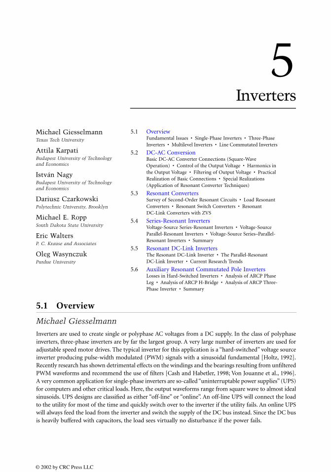
5Inverters
5.1 OverviewFundamental Issues • Single-Phase Inverters • Three-Phase Inverters • Multilevel Inverters • Line Commutated Inverters
5.2 DC-AC ConversionBasic DC-AC Converter Connections (Square-Wave Operation) • Control of the Output Voltage • Harmonics in the Output Voltage • Filtering of Output Voltage • Practical Realization of Basic Connections • Special Realizations (Application of Resonant Converter Techniques)
5.3 Resonant ConvertersSurvey of Second-Order Resonant Circuits • Load Resonant Converters • Resonant Switch Converters • Resonant DC-Link Converters with ZVS
5.4 Series-Resonant InvertersVoltage-Source Series-Resonant Inverters • Voltage-Source Parallel-Resonant Inverters • Voltage-Source Series–Parallel-Resonant Inverters • Summary
5.5 Resonant DC-Link InvertersThe Resonant DC-Link Inverter • The Parallel-Resonant DC-Link Inverter • Current Research Trends
5.6 Auxiliary Resonant Commutated Pole InvertersLosses in Hard-Switched Inverters • Analysis of ARCP Phase Leg • Analysis of ARCP H-Bridge • Analysis of ARCP Three-Phase Inverter • Summary
5.1 Overview
Michael Giesselmann
Inverters are used to create single or polyphase AC voltages from a DC supply. In the class of polyphaseinverters, three-phase inverters are by far the largest group. A very large number of inverters are used foradjustable speed motor drives. The typical inverter for this application is a “hard-switched” voltage sourceinverter producing pulse-width modulated (PWM) signals with a sinusoidal fundamental [Holtz, 1992].Recently research has shown detrimental effects on the windings and the bearings resulting from unfilteredPWM waveforms and recommend the use of filters [Cash and Habetler, 1998; Von Jouanne et al., 1996].A very common application for single-phase inverters are so-called “uninterruptable power supplies” (UPS)for computers and other critical loads. Here, the output waveforms range from square wave to almost idealsinusoids. UPS designs are classified as either “off-line” or “online”. An off-line UPS will connect the loadto the utility for most of the time and quickly switch over to the inverter if the utility fails. An online UPSwill always feed the load from the inverter and switch the supply of the DC bus instead. Since the DC busis heavily buffered with capacitors, the load sees virtually no disturbance if the power fails.
Michael GiesselmannTexas Tech University
Attila KarpatiBudapest University of Technology and Economics
István NagyBudapest University of Technology and Economics
Dariusz CzarkowskiPolytechnic University, Brooklyn
Michael E. RoppSouth Dakota State University
Eric WaltersP. C. Krause and Associates
Oleg WasynczukPurdue University
© 2002 by CRC Press LLC
In addition to the very common hard-switched inverters, active research is being conducted on soft-switching techniques. Hard-switched inverters use controllable power semiconductors to connect an outputterminal to a stable DC bus. On the other hand, soft switching inverters have an oscillating intermediatecircuit and attempt to open and close the power switches under zero-voltage and or zero-currentconditions.
A separate class of inverters are the line commutated inverters for multimegawatt power ratings, that usethyristors (also called silicon controlled rectifiers, SCRs). SCRs can only be turned “on” on command. Afterbeing turned on, the current in the device must approach zero in order to turn the device off. All otherinverters are self-commutated, meaning that the power control devices can be turned on and off. Linecommutated inverters need the presence of a stable utility voltage to function. They are used for DC-linksbetween utilities, ultralong distance energy transport, and very large motor drives [Ahmed, 1999; Barton,1994; Mohan et al., 1995; Rashid, 1993; Tarter, 1993]. However, the latter application is more and moretaken over by modern hard-switched inverters including multilevel inverters [Brumsickle et al., 1998; Tolbertet al., 1999].
Modern inverters use insulated gate bipolar transistors (IGBTs) as the main power control devices[Mohan et al., 1995]. Besides IGBTs, power MOSFETs are also used especially for lower voltages, powerratings, and applications that require high efficiency and high switching frequency. In recent years, IGBTs,MOSFETs, and their control and protection circuitry have made remarkable progress. IGBTs are nowavailable with voltage ratings of up to 3300 V and current ratings up to 1200 A. MOSFETs have achievedon-state resistances approaching a few milliohms. In addition to the devices, manufacturers today offercustomized control circuitry that provides for electrical isolation, proper operation of the devices undernormal operating conditions and protection from a variety of fault conditions [Mohan et al., 1995]. Inaddition, the industry provides good support for specialized passive devices such as capacitors andmechanical components such as low inductance bus-bar assemblies to facilitate the design of reliableinverters. In addition to the aforementioned inverters, a large number of special topologies are used. Agood overview is given by Gottlieb [1984].
Fundamental Issues
Inverters fall in the class of power electronics circuits. The most widely accepted definition of a powerelectronics circuit is that the circuit is actually processing electric energy rather than information. Theactual power level is not very important for the classification of a circuit as a power electronics circuit.One of the most important performance considerations of power electronics circuits, like inverters, istheir energy conversion efficiency. The most important reason for demanding high efficiency is theproblem of removing large amounts of heat from the power devices. Of course, the judicious use ofenergy is also paramount, especially if the inverter is fed from batteries such as in electric cars. For thesereasons, inverters operate the power devices, which control the flow of energy, as switches. In the idealcase of a switching event, there would be no power loss in the switch since either the current in the switchis zero (switch open) or the voltage across the switch is zero (switch closed) and the power loss is computedas the product of both. In reality, there are two mechanisms that do create some losses, however; theseare on-state losses and switching losses [Bird et al., 1993; Kassakian et al., 1991; Mohan et al., 1995;Rashid, 1993]. On-state losses are due to the fact that the voltage across the switch in the on state is notzero, but typically in the range of 1 to 2 V for IGBTs. For power MOSFETs, the on-state voltage is oftenin the same range, but it can be substantially below 0.5 V due to the fact that these devices have a purelyresistive conduction channel and no fixed minimum saturation voltage like bipolar junction devices(IGBTs). The switching losses are the second major loss mechanism and are due to the fact that, duringthe turn-on and turn-off transition, current is flowing while voltage is present across the device. In orderto minimize the switching losses, the individual transitions have to be rapid (tens to hundreds ofnanoseconds) and the maximum switching frequency needs to be carefully considered.
In order to avoid audible noise being radiated from motor windings or transformers, most moderninverters operate at switching frequencies substantially above 10 kHz [Bose, 1992; 1996].
© 2002 by CRC Press LLC
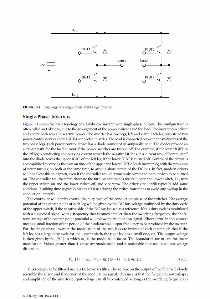
Single-Phase Inverters
Figure 5.1 shows the basic topology of a full-bridge inverter with single-phase output. This configuration isoften called an H-bridge, due to the arrangement of the power switches and the load. The inverter can deliverand accept both real and reactive power. The inverter has two legs, left and right. Each leg consists of twopower control devices (here IGBTs) connected in series. The load is connected between the midpoints of thetwo phase legs. Each power control device has a diode connected in antiparallel to it. The diodes provide analternate path for the load current if the power switches are turned off. For example, if the lower IGBT inthe left leg is conducting and carrying current towards the negative DC bus, this current would “commutate”into the diode across the upper IGBT of the left leg, if the lower IGBT is turned off. Control of the circuit isaccomplished by varying the turn on time of the upper and lower IGBT of each inverter leg, with the provisionof never turning on both at the same time, to avoid a short circuit of the DC bus. In fact, modern driverswill not allow this to happen, even if the controller would erroneously command both devices to be turnedon. The controller will therefore alternate the turn on commands for the upper and lower switch, i.e., turnthe upper switch on and the lower switch off, and vice versa. The driver circuit will typically add someadditional blanking time (typically 500 to 1000 ns) during the switch transitions to avoid any overlap in theconduction intervals.
The controller will hereby control the duty cycle of the conduction phase of the switches. The averagepotential of the center-point of each leg will be given by the DC bus voltage multiplied by the duty cycleof the upper switch, if the negative side of the DC bus is used as a reference. If this duty cycle is modulatedwith a sinusoidal signal with a frequency that is much smaller than the switching frequency, the short-term average of the center-point potential will follow the modulation signal. “Short-term” in this contextmeans a small fraction of the period of the fundamental output frequency to be produced by the inverter.For the single phase inverter, the modulation of the two legs are inverse of each other such that if theleft leg has a large duty cycle for the upper switch, the right leg has a small one, etc. The output voltageis then given by Eq. (5.1) in which ma is the modulation factor. The boundaries for ma are for linearmodulation. Values greater than 1 cause overmodulation and a noticeable increase in output voltagedistortion.
(5.1)
This voltage can be filtered using a LC low-pass filter. The voltage on the output of the filter will closelyresemble the shape and frequency of the modulation signal. This means that the frequency, wave-shape,and amplitude of the inverter output voltage can all be controlled as long as the switching frequency is
FIGURE 5.1 Topology of a single-phase, full-bridge inverter.
Vac1 t( ) ma Vdc w1 t⋅( ) 0 ma 1≤ ≤sin⋅ ⋅=
© 2002 by CRC Press LLC
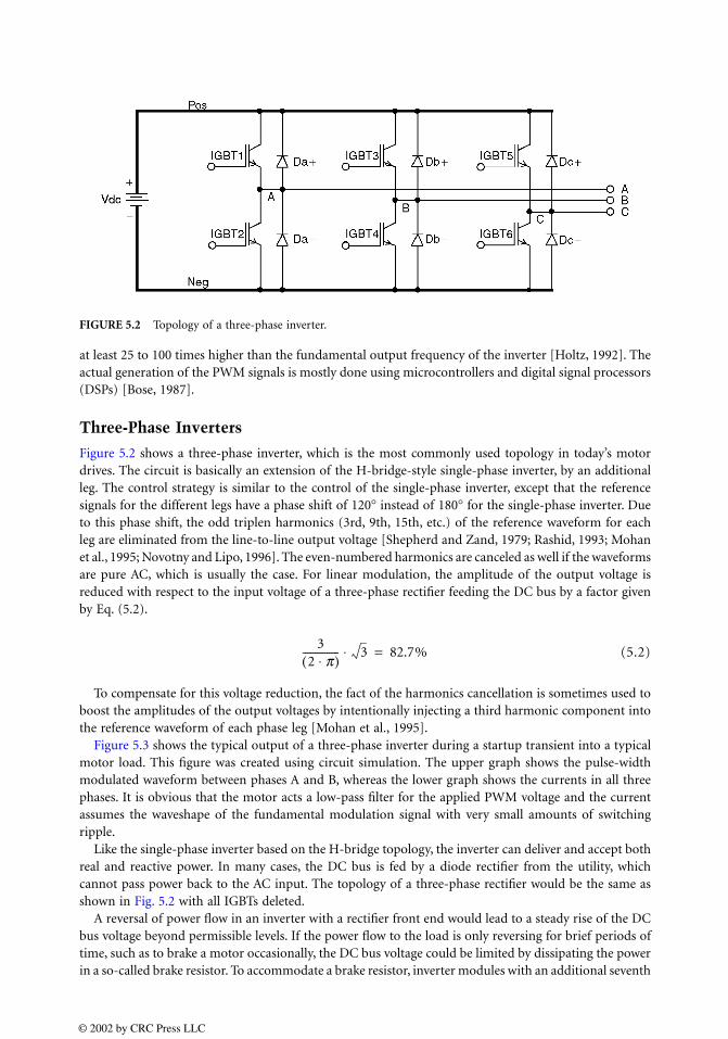
at least 25 to 100 times higher than the fundamental output frequency of the inverter [Holtz, 1992]. Theactual generation of the PWM signals is mostly done using microcontrollers and digital signal processors(DSPs) [Bose, 1987].
Three-Phase Inverters
Figure 5.2 shows a three-phase inverter, which is the most commonly used topology in today’s motordrives. The circuit is basically an extension of the H-bridge-style single-phase inverter, by an additionalleg. The control strategy is similar to the control of the single-phase inverter, except that the referencesignals for the different legs have a phase shift of 120° instead of 180° for the single-phase inverter. Dueto this phase shift, the odd triplen harmonics (3rd, 9th, 15th, etc.) of the reference waveform for eachleg are eliminated from the line-to-line output voltage [Shepherd and Zand, 1979; Rashid, 1993; Mohanet al., 1995; Novotny and Lipo, 1996]. The even-numbered harmonics are canceled as well if the waveformsare pure AC, which is usually the case. For linear modulation, the amplitude of the output voltage isreduced with respect to the input voltage of a three-phase rectifier feeding the DC bus by a factor givenby Eq. (5.2).
(5.2)
To compensate for this voltage reduction, the fact of the harmonics cancellation is sometimes used toboost the amplitudes of the output voltages by intentionally injecting a third harmonic component intothe reference waveform of each phase leg [Mohan et al., 1995].
Figure 5.3 shows the typical output of a three-phase inverter during a startup transient into a typicalmotor load. This figure was created using circuit simulation. The upper graph shows the pulse-widthmodulated waveform between phases A and B, whereas the lower graph shows the currents in all threephases. It is obvious that the motor acts a low-pass filter for the applied PWM voltage and the currentassumes the waveshape of the fundamental modulation signal with very small amounts of switchingripple.
Like the single-phase inverter based on the H-bridge topology, the inverter can deliver and accept bothreal and reactive power. In many cases, the DC bus is fed by a diode rectifier from the utility, whichcannot pass power back to the AC input. The topology of a three-phase rectifier would be the same asshown in Fig. 5.2 with all IGBTs deleted.
A reversal of power flow in an inverter with a rectifier front end would lead to a steady rise of the DCbus voltage beyond permissible levels. If the power flow to the load is only reversing for brief periods oftime, such as to brake a motor occasionally, the DC bus voltage could be limited by dissipating the powerin a so-called brake resistor. To accommodate a brake resistor, inverter modules with an additional seventh
FIGURE 5.2 Topology of a three-phase inverter.
32 p⋅( )
--------------- 3⋅ 82.7%=
© 2002 by CRC Press LLC
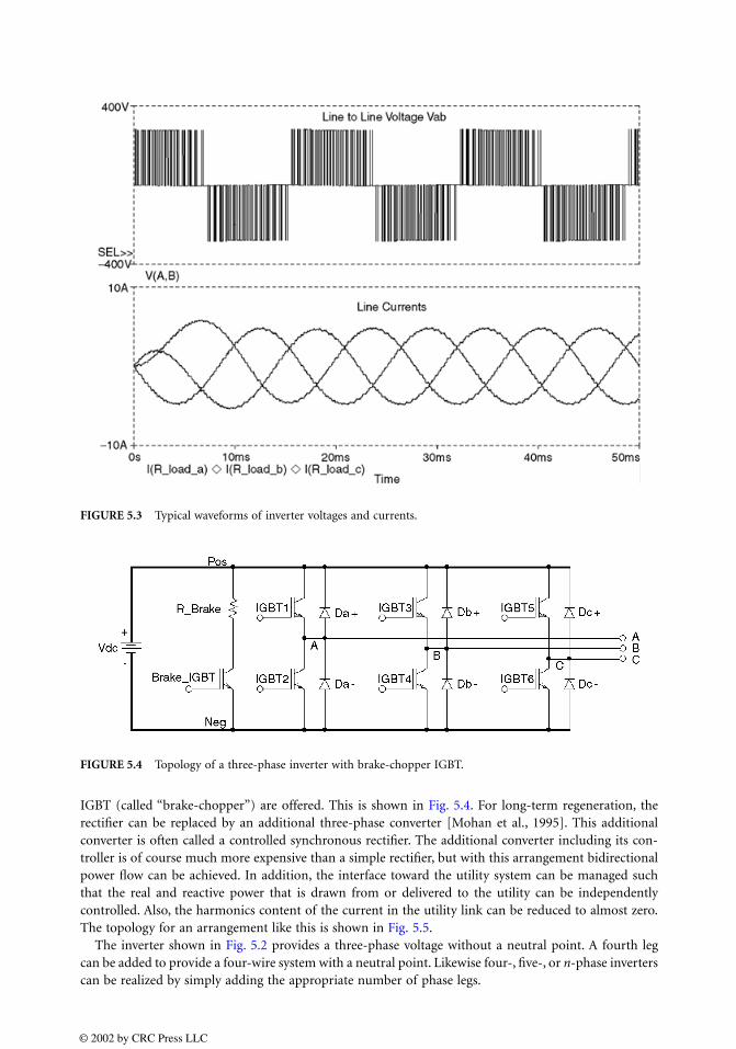
IGBT (called “brake-chopper”) are offered. This is shown in Fig. 5.4. For long-term regeneration, therectifier can be replaced by an additional three-phase converter [Mohan et al., 1995]. This additionalconverter is often called a controlled synchronous rectifier. The additional converter including its con-troller is of course much more expensive than a simple rectifier, but with this arrangement bidirectionalpower flow can be achieved. In addition, the interface toward the utility system can be managed suchthat the real and reactive power that is drawn from or delivered to the utility can be independentlycontrolled. Also, the harmonics content of the current in the utility link can be reduced to almost zero.The topology for an arrangement like this is shown in Fig. 5.5.
The inverter shown in Fig. 5.2 provides a three-phase voltage without a neutral point. A fourth legcan be added to provide a four-wire system with a neutral point. Likewise four-, five-, or n-phase inverterscan be realized by simply adding the appropriate number of phase legs.
FIGURE 5.3 Typical waveforms of inverter voltages and currents.
FIGURE 5.4 Topology of a three-phase inverter with brake-chopper IGBT.
© 2002 by CRC Press LLC

As in single-phase inverters, the generation of the PWM control signals is done using modern micro-controllers and DSPs. These digital controllers are typically not only controlling just the inverter, butthrough the controlled synthesis of the appropriate voltages, motors and attached loads are controlledfor high-performance dynamic response. The most commonly used control principle for superiordynamic response is called field-oriented or vector control [Bose, 1987; 1996; DeDonker and Novotny,1988; Lorenz and Divan, 1990; Trzynadlowski, 1994].
Multilevel Inverters
Multilevel inverters are a class of inverters where a DC source with several tabs between the positive andnegative terminal is present. The two main advantages of multilevel inverters are the higher voltagecapability and the reduced harmonics content of the output waveform due to the multiple DC levels.The higher voltage capability is due to the fact that clamping diodes are used to limit the voltage stresson the IGBTs to the voltage differential between two tabs on the DC bus. Figure 5.6 shows the topologyof a three-level inverter. Here, each phase leg consists of four IGBTs in series with additional antiparallel
FIGURE 5.5 Topology of a three-phase inverter system for bidirectional power flow.
FIGURE 5.6 Topology of a three-level inverter.
© 2002 by CRC Press LLC
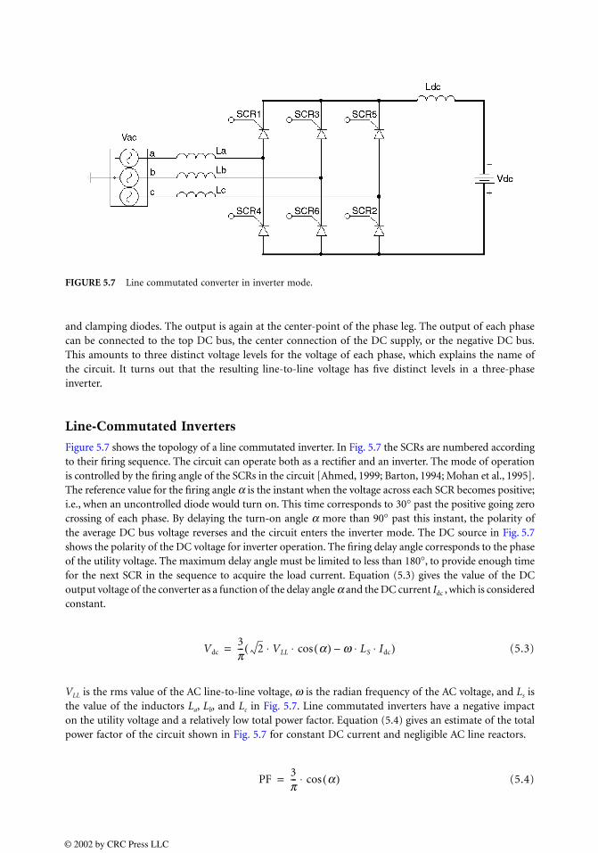
and clamping diodes. The output is again at the center-point of the phase leg. The output of each phasecan be connected to the top DC bus, the center connection of the DC supply, or the negative DC bus.This amounts to three distinct voltage levels for the voltage of each phase, which explains the name ofthe circuit. It turns out that the resulting line-to-line voltage has five distinct levels in a three-phaseinverter.
Line-Commutated Inverters
Figure 5.7 shows the topology of a line commutated inverter. In Fig. 5.7 the SCRs are numbered accordingto their firing sequence. The circuit can operate both as a rectifier and an inverter. The mode of operationis controlled by the firing angle of the SCRs in the circuit [Ahmed, 1999; Barton, 1994; Mohan et al., 1995].The reference value for the firing angle α is the instant when the voltage across each SCR becomes positive;i.e., when an uncontrolled diode would turn on. This time corresponds to 30° past the positive going zerocrossing of each phase. By delaying the turn-on angle α more than 90° past this instant, the polarity ofthe average DC bus voltage reverses and the circuit enters the inverter mode. The DC source in Fig. 5.7shows the polarity of the DC voltage for inverter operation. The firing delay angle corresponds to the phaseof the utility voltage. The maximum delay angle must be limited to less than 180°, to provide enough timefor the next SCR in the sequence to acquire the load current. Equation (5.3) gives the value of the DCoutput voltage of the converter as a function of the delay angle α and the DC current Idc , which is consideredconstant.
(5.3)
VLL is the rms value of the AC line-to-line voltage, ω is the radian frequency of the AC voltage, and Ls isthe value of the inductors La, Lb, and Lc in Fig. 5.7. Line commutated inverters have a negative impacton the utility voltage and a relatively low total power factor. Equation (5.4) gives an estimate of the totalpower factor of the circuit shown in Fig. 5.7 for constant DC current and negligible AC line reactors.
(5.4)
FIGURE 5.7 Line commutated converter in inverter mode.
Vdc3p--- 2 VLL a( )cos w– LS Idc⋅ ⋅ ⋅ ⋅( )=
PF3p--- a( )cos⋅=
© 2002 by CRC Press LLC

References
Ahmed, A., Power Electronics for Technology, Prentice-Hall, Upper Saddle River, NJ, 1999. Barton, T. H., Rectifiers, Cycloconverters, and AC Controllers, Oxford University Press, New York, 1994.Bird, B. M., King, K. G., and Pedder, D. A. G., An Introduction to Power Electronics, 2nd ed., John Wiley
& Sons, New York, 1993.Bose, B. K., Modern Power Electronics, Evolution, Technology, and Applications, IEEE Press, Piscataway,
NJ, 1992.Bose, B. K., Microcomputer Control of Power Electronics and Drives, IEEE Press, Piscataway, NJ, 1987.Bose, B. K., Power Electronics and Variable Frequency Drives, IEEE Press, Piscataway, NJ, 1996.Brumsickle, W. E., Divan, D. M., and Lipo, T. A., Reduced switching stress in high-voltage IGBT inverters
via a three-level structure, IEEE-APEC 2. 544–550, Feb. 1998.Cash, M. A. and Habetler, T. G., Insulation failure prediction in induction machines using line-neutral
voltages, IEEE Trans. Ind. Appl., 34(6), 1234–1239, Nov./Dec. 1998.De Donker, R. and Novotny, D. W., The universal field-oriented controller, Conf. Rec. IEEE-IAS 1988,
450–456.Gottlieb, I. M., Power Supplies, Switching Regulators, Inverters and Converters, TAB Books, Blue Ridge
Summit, PA, 1984.Holtz, J., Pulsewidth modulation—a survey, IEEE Trans. Ind. Electr., 39(5), 410–420, 1992.Kassakian, J. G., Schlecht, M. F., and Verghese, G. C., Principles of Power Electronics, Addison-Wesley,
Reading, MA, 1991.Lorenz, R. D. and Divan, D. M., Dynamic analysis and experimental evaluation of delta modulators for
field oriented induction machines, IEEE Trans. Ind. Appl., 26(2), 296–301, 1990.Mohan, N., Undeland, T., and Robbins, W., Power Electronics: Converters, Applications, and Design, 2nd ed.,
John Wiley & Sons, New York, 1995.Novotny, D. W. and Lipo, T. A., Vector Control and Dynamics of AC Drives, Oxford Science Publications,
New York, 1996.Rashid, M. H., Power Electronics, Circuits, Devices, and Applications, Prentice-Hall, Englewood Cliffs, NJ,
1993.Shepherd, W. and Zand, P., Energy Flow and Power Factor in Nonsinusoidal Circuits, Cambridge University
Press, London, 1979.Tarter, R. E., Solid State Power Conversion Handbook, John Wiley & Sons, New York, 1993.Tolbert, L. M., Peng, F. Z., and Habetler, T. G., Multilevel converters for large electric drives, IEEE Trans.
Ind. Appl., 35(1), 36–44, Jan./Feb. 1999.Trzynadlowski, A. M., The Field Orientation Principle in Control of Induction Motors, Kluwer Academic
Publishers, Dordrecht, the Netherlands, 1994.Von Jouanne, A., Rendusara, D., Enjeti, P., and Gray, W., Filtering techniques to minimize the effect of
long motor leads on PWM inverter fed AC motor drive systems, IEEE Trans. Ind. Appl., 32(4),919–926, July/Aug. 1996.
5.2 DC-AC Conversion
Attila Karpati
The DC-AC converters, also known as inverters and shown in Fig. 5.8, produce an AC voltage from aDC input voltage. The frequency and amplitude produced are generally variable. In practice, inverterswith both single-phase and three-phase outputs are used, but other phase numbers are also possible.Electric power usually flows from the DC to the AC terminal, but in some cases reverse power flow ispossible. These types of inverters, where the input is a DC voltage source, are also known as voltage-source inverters (VSI). The other type of inverter is the current-source inverters (CSI), where the DCinput is a DC current source. These converters are used primarily in high-power AC motor drives.
© 2002 by CRC Press LLC
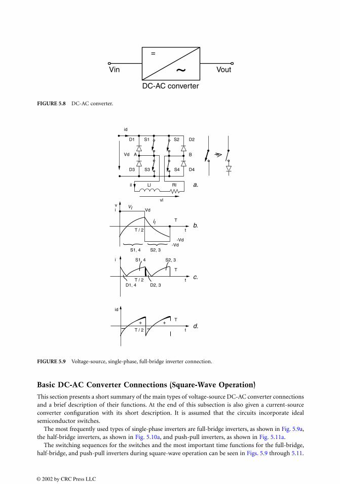
Basic DC-AC Converter Connections (Square-Wave Operation)
This section presents a short summary of the main types of voltage-source DC-AC converter connectionsand a brief description of their functions. At the end of this subsection is also given a current-sourceconverter configuration with its short description. It is assumed that the circuits incorporate idealsemiconductor switches.
The most frequently used types of single-phase inverters are full-bridge inverters, as shown in Fig. 5.9a,the half-bridge inverters, as shown in Fig. 5.10a, and push-pull inverters, as shown in Fig. 5.11a.
The switching sequences for the switches and the most important time functions for the full-bridge,half-bridge, and push-pull inverters during square-wave operation can be seen in Figs. 5.9 through 5.11.
FIGURE 5.8 DC-AC converter.
FIGURE 5.9 Voltage-source, single-phase, full-bridge inverter connection.
Vin Vout
DC-AC converter
=
~
id
D1
D3 S3 S4 D4
S1 S2 D2
BVd A
il
vVd
-Vd-Vd
T
T
T
T / 2
T / 2
T / 2
S1, 4
D1, 4
S1, 4
S2, 3
D2, 3
S2, 3
Ll
vl
Rl a.
b.
c.
d.
i
i
id
Vl
ilt
t
t
+ +
© 2002 by CRC Press LLC
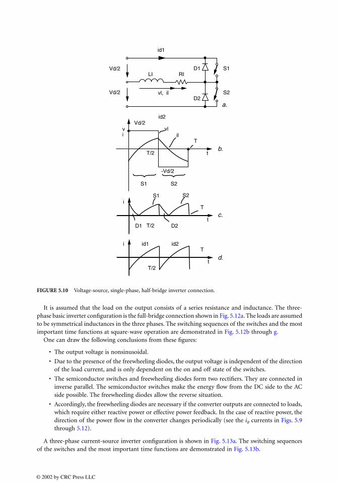
It is assumed that the load on the output consists of a series resistance and inductance. The three-phase basic inverter configuration is the full-bridge connection shown in Fig. 5.12a. The loads are assumedto be symmetrical inductances in the three phases. The switching sequences of the switches and the mostimportant time functions at square-wave operation are demonstrated in Fig. 5.12b through g.
One can draw the following conclusions from these figures:
• The output voltage is nonsinusoidal.
• Due to the presence of the freewheeling diodes, the output voltage is independent of the directionof the load current, and is only dependent on the on and off state of the switches.
• The semiconductor switches and freewheeling diodes form two rectifiers. They are connected ininverse parallel. The semiconductor switches make the energy flow from the DC side to the ACside possible. The freewheeling diodes allow the reverse situation.
• Accordingly, the freewheeling diodes are necessary if the converter outputs are connected to loads,which require either reactive power or effective power feedback. In the case of reactive power, thedirection of the power flow in the converter changes periodically (see the iB currents in Figs. 5.9through 5.12).
A three-phase current-source inverter configuration is shown in Fig. 5.13a. The switching sequencesof the switches and the most important time functions are demonstrated in Fig. 5.13b.
FIGURE 5.10 Voltage-source, single-phase, half-bridge inverter connection.
id1
id2
Vd/2
Vd/2
Vd/2
-Vd/2
T/2
T/2
T/2
LI RID1 S1
S2D2
S1 S2
S2S1
D1 D2
vl, il
vi il
vl
T
T
T
t
t
t
i
i id1 id2
a.
b.
c.
d.
© 2002 by CRC Press LLC
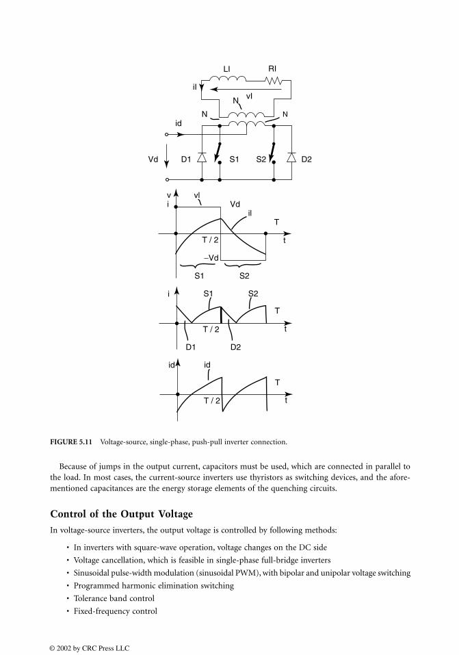
Because of jumps in the output current, capacitors must be used, which are connected in parallel tothe load. In most cases, the current-source inverters use thyristors as switching devices, and the afore-mentioned capacitances are the energy storage elements of the quenching circuits.
Control of the Output Voltage
In voltage-source inverters, the output voltage is controlled by following methods:
• In inverters with square-wave operation, voltage changes on the DC side
• Voltage cancellation, which is feasible in single-phase full-bridge inverters
• Sinusoidal pulse-width modulation (sinusoidal PWM), with bipolar and unipolar voltage switching
• Programmed harmonic elimination switching
• Tolerance band control
• Fixed-frequency control
FIGURE 5.11 Voltage-source, single-phase, push-pull inverter connection.
LI
iI
RI
N
N
N
vI
id
Vd
v vlVd
il
D1 S1 S2 D2
i
T
T
T
T / 2
T / 2
T / 2
−Vd
S1
S1
D1 D2
S2
S2
i
id id
t
t
t
© 2002 by CRC Press LLC
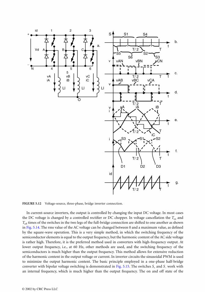
In current-source inverters, the output is controlled by changing the input DC voltage. In most casesthe DC voltage is changed by a controlled rectifier or DC chopper. In voltage cancellation the Ton andToff times of the switches in the two legs of the full-bridge connection are shifted to one another as shownin Fig. 5.14. The rms value of the AC voltage can be changed between 0 and a maximum value, as definedby the square-wave operation. This is a very simple method, in which the switching frequency of thesemiconductor elements is equal to the output frequency, but the harmonic content of the AC side voltageis rather high. Therefore, it is the preferred method used in converters with high-frequency output. Atlower output frequency, i.e., at 60 Hz, other methods are used, and the switching frequency of thesemiconductors is much higher than the output frequency. This method allows for extensive reductionof the harmonic content in the output voltage or current. In inverter circuits the sinusoidal PWM is usedto minimize the output harmonic content. The basic principle employed in a one-phase half-bridgeconverter with bipolar voltage switching is demonstrated in Fig. 5.15. The switches S+ and S− work withan internal frequency, which is much higher than the output frequency. The on and off state of the
FIGURE 5.12 Voltage-source, three-phase, bridge inverter connection.
id+
−
1 2 3
A B C
4 55
6
Vd
N
vA vB vCiA iB iC
v
b.
c.
d.
e.
f.
g.t
t
t
t
t
t
Ll Ll Ll
T/ 2
T/ 2
T/ 2
T/ 2
T/ 2
T
T
T
T
T/ 2 T
T
D1 D2 D3
id
i S3 S1 S2iC
vi
vA iA iB
vvAB
vAN vBN vCN
vBC vCA
S5S6
S2S3
S1 S4S
a.
O
© 2002 by CRC Press LLC
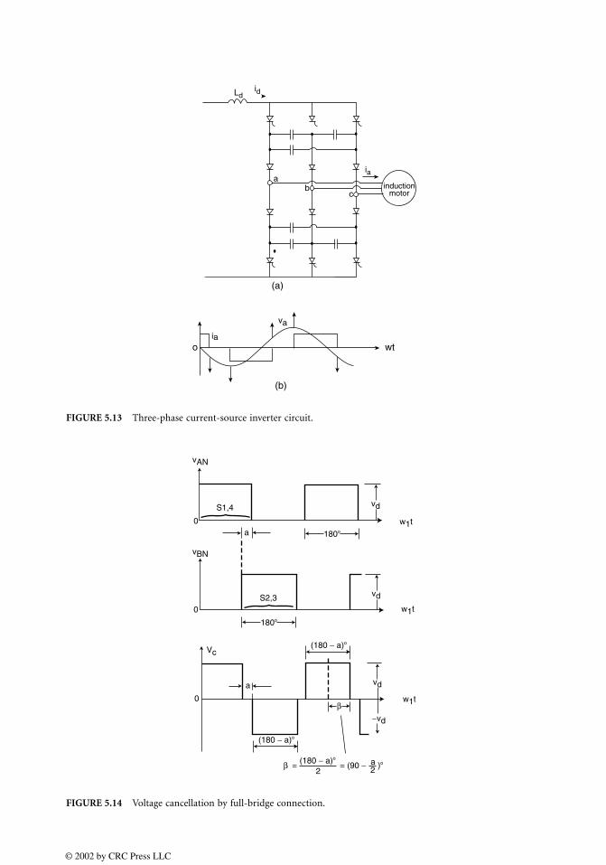
FIGURE 5.13 Three-phase current-source inverter circuit.
FIGURE 5.14 Voltage cancellation by full-bridge connection.
Ldid
ia
va
ia
inductionmotor
ab
c
(a)
(b)
wto
vAN
vBN
0
0
0
Vc
vd
vd
vd
−vd
w1t
w1t
w1t
S1,4
S2,3
a
a
180o
(180 − a)o
(180 − a)o
(180 − a)o
2a2β = = (90 − )o
180o
β
© 2002 by CRC Press LLC
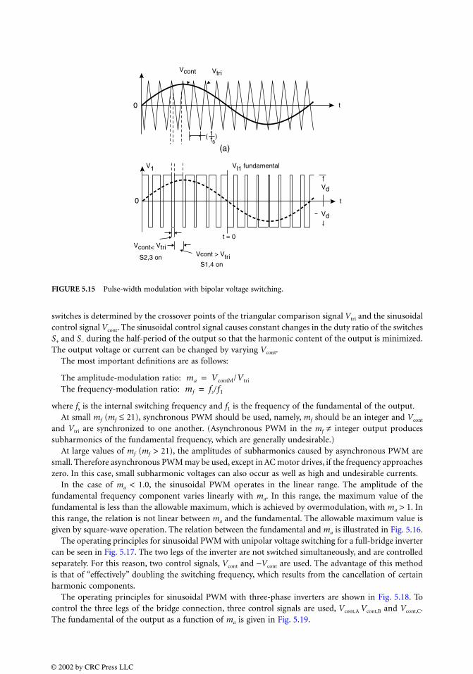
switches is determined by the crossover points of the triangular comparison signal Vtri and the sinusoidalcontrol signal Vcont. The sinusoidal control signal causes constant changes in the duty ratio of the switchesS+ and S− during the half-period of the output so that the harmonic content of the output is minimized.The output voltage or current can be changed by varying Vcont.
The most important definitions are as follows:
The amplitude-modulation ratio:The frequency-modulation ratio:
where fs is the internal switching frequency and f1 is the frequency of the fundamental of the output.At small mf (mf ≤ 21), synchronous PWM should be used, namely, mf should be an integer and Vcont
and Vtri are synchronized to one another. (Asynchronous PWM in the mf ≠ integer output producessubharmonics of the fundamental frequency, which are generally undesirable.)
At large values of mf (mf > 21), the amplitudes of subharmonics caused by asynchronous PWM aresmall. Therefore asynchronous PWM may be used, except in AC motor drives, if the frequency approacheszero. In this case, small subharmonic voltages can also occur as well as high and undesirable currents.
In the case of ma < 1.0, the sinusoidal PWM operates in the linear range. The amplitude of thefundamental frequency component varies linearly with ma. In this range, the maximum value of thefundamental is less than the allowable maximum, which is achieved by overmodulation, with ma > 1. Inthis range, the relation is not linear between ma and the fundamental. The allowable maximum value isgiven by square-wave operation. The relation between the fundamental and ma is illustrated in Fig. 5.16.
The operating principles for sinusoidal PWM with unipolar voltage switching for a full-bridge invertercan be seen in Fig. 5.17. The two legs of the inverter are not switched simultaneously, and are controlledseparately. For this reason, two control signals, Vcont and −Vcont are used. The advantage of this methodis that of “effectively” doubling the switching frequency, which results from the cancellation of certainharmonic components.
The operating principles for sinusoidal PWM with three-phase inverters are shown in Fig. 5.18. Tocontrol the three legs of the bridge connection, three control signals are used, Vcont,A Vcont,B and Vcont,C.The fundamental of the output as a function of ma is given in Fig. 5.19.
FIGURE 5.15 Pulse-width modulation with bipolar voltage switching.
Vcont
Vcont< VtriVcont > Vtri
V1
Vd
Vd
Vl1 fundamental
Vtri
(a)
t
t
0
0
( )1fs
t = 0
S1,4 onS2,3 on
ma VcontM/Vtri=mf fs/f1=
© 2002 by CRC Press LLC
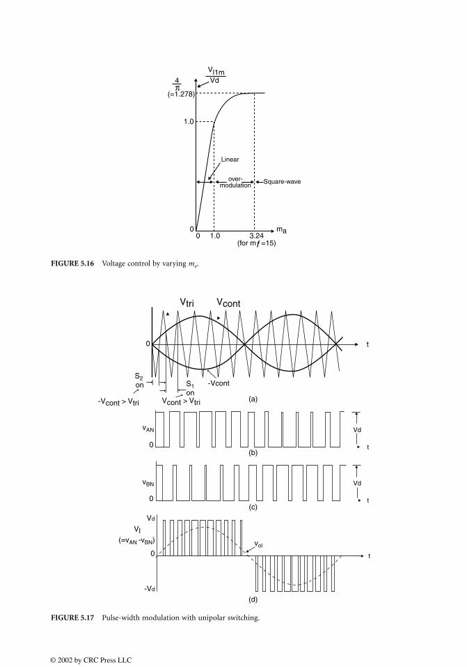
FIGURE 5.16 Voltage control by varying ma.
FIGURE 5.17 Pulse-width modulation with unipolar switching.
Vl1mVd4
(=1.278)π
1.0
Linear
over-modulation
00 1.0 3.24
(for mf =15)
ma
Square-wave
Vtri
-Vcont > Vtri Vcont > Vtri
Vcont
0
onon
(a)
(b)
(c)
(d)
S2S1 -Vcont
Vd
Vd
t
vAN
(=vAN -vBN)
vBN
vol
Vd
-Vd
Vl
0
0
0
t
t
t
© 2002 by CRC Press LLC
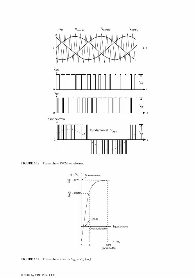
FIGURE 5.18 Three-phase PWM waveforms.
FIGURE 5.19 Three-phase inverter VLi1 = VLi1 (ma).
vtri
vAN
vBN
vAB=vAN-vBN
Fundamental VAB1
Vcont,A
Vd
Vd
Vd
Vcont,B Vcont,C
0
0
0
0 t
t
t
t
π∼_ 0.78
∼_ 0.612
Square-wave
Square-wave
6
32
VLI1/Vd
Linear
Overmodulation
3.24(for mf =15)
ma0 1
© 2002 by CRC Press LLC
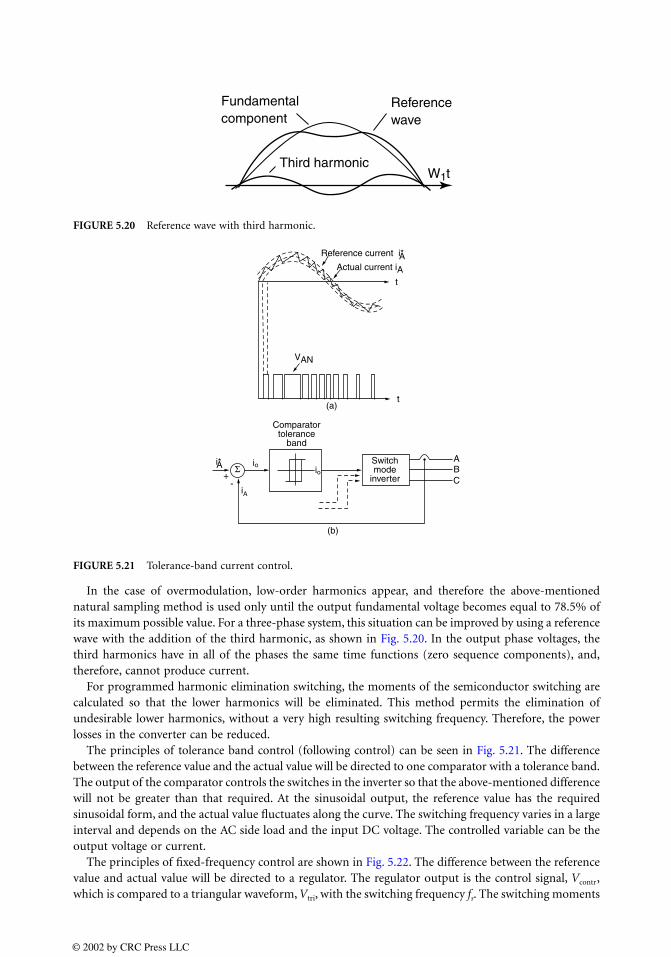
In the case of overmodulation, low-order harmonics appear, and therefore the above-mentionednatural sampling method is used only until the output fundamental voltage becomes equal to 78.5% ofits maximum possible value. For a three-phase system, this situation can be improved by using a referencewave with the addition of the third harmonic, as shown in Fig. 5.20. In the output phase voltages, thethird harmonics have in all of the phases the same time functions (zero sequence components), and,therefore, cannot produce current.
For programmed harmonic elimination switching, the moments of the semiconductor switching arecalculated so that the lower harmonics will be eliminated. This method permits the elimination ofundesirable lower harmonics, without a very high resulting switching frequency. Therefore, the powerlosses in the converter can be reduced.
The principles of tolerance band control (following control) can be seen in Fig. 5.21. The differencebetween the reference value and the actual value will be directed to one comparator with a tolerance band.The output of the comparator controls the switches in the inverter so that the above-mentioned differencewill not be greater than that required. At the sinusoidal output, the reference value has the requiredsinusoidal form, and the actual value fluctuates along the curve. The switching frequency varies in a largeinterval and depends on the AC side load and the input DC voltage. The controlled variable can be theoutput voltage or current.
The principles of fixed-frequency control are shown in Fig. 5.22. The difference between the referencevalue and actual value will be directed to a regulator. The regulator output is the control signal, Vcontr,which is compared to a triangular waveform, Vtri, with the switching frequency fs. The switching moments
FIGURE 5.20 Reference wave with third harmonic.
FIGURE 5.21 Tolerance-band current control.
Fundamentalcomponent
Referencewave
Third harmonicW1t
Reference current i*
Actual current iA
VAN
(a)
Comparatortolerance
band
i*A+
-
io
iA
ioABC
Switchmode
inverter
t
t
(b)
Σ
A
© 2002 by CRC Press LLC
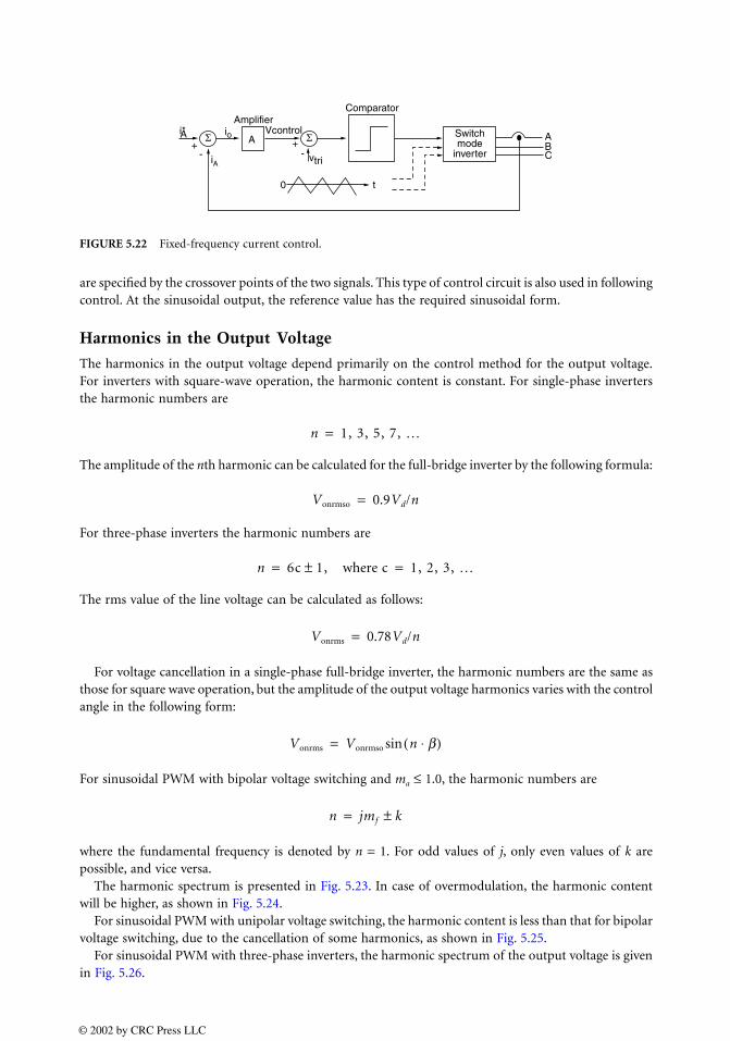
are specified by the crossover points of the two signals. This type of control circuit is also used in followingcontrol. At the sinusoidal output, the reference value has the required sinusoidal form.
Harmonics in the Output Voltage
The harmonics in the output voltage depend primarily on the control method for the output voltage.For inverters with square-wave operation, the harmonic content is constant. For single-phase invertersthe harmonic numbers are
The amplitude of the nth harmonic can be calculated for the full-bridge inverter by the following formula:
For three-phase inverters the harmonic numbers are
The rms value of the line voltage can be calculated as follows:
For voltage cancellation in a single-phase full-bridge inverter, the harmonic numbers are the same asthose for square wave operation, but the amplitude of the output voltage harmonics varies with the controlangle in the following form:
For sinusoidal PWM with bipolar voltage switching and ma ≤ 1.0, the harmonic numbers are
where the fundamental frequency is denoted by n = 1. For odd values of j, only even values of k arepossible, and vice versa.
The harmonic spectrum is presented in Fig. 5.23. In case of overmodulation, the harmonic contentwill be higher, as shown in Fig. 5.24.
For sinusoidal PWM with unipolar voltage switching, the harmonic content is less than that for bipolarvoltage switching, due to the cancellation of some harmonics, as shown in Fig. 5.25.
For sinusoidal PWM with three-phase inverters, the harmonic spectrum of the output voltage is givenin Fig. 5.26.
FIGURE 5.22 Fixed-frequency current control.
ComparatorAmplifier
i*A+ +
- -
io
iA
ABC
Switchmode
inverter
Σ ΣA
0 t
Vcontrol
vtri
n 1, 3, 5, 7, …=
Vonrmso 0.9Vd/n=
n 6c 1, where c± 1, 2, 3, …= =
Vonrms 0.78Vd/n=
Vonrms Vonrmso n β⋅( )sin=
n jmf k±=
© 2002 by CRC Press LLC

FIGURE 5.23 Single-phase full-bridge.
FIGURE 5.24 Single-phase full-bridge with bipolar switching, harmonic spectrum.
FIGURE 5.25 Single-phase full-bridge with unipolar switching, harmonic spectrum.
FIGURE 5.26 Three-phase PWM, harmonic spectrum.
VlnmVd
ma =0.8 mf = 15
1 mf
Harmonics n of f 1
2mf(2mf + 1)(mf + 2) (3mf + 2)
3mf
1.21.10.80.60.40.20.0
VlnmVd
1.0
0.5
0 1 3 5 7 9 11 13 15 17 19 21 23 25 27Harmonics S,N
Harmonics due to overmodulation; figure is drawn for ma = 2.5and mf = 15 (single - phase full - bridge)
Ma =2.5Mf =15
(mf)
N
Vlnm
1.00.80.60.40.2
01 mf 2mf
(2mf -1) (2mf +1)(Harmonics of f 1)
3mf 4mf
Vd
VLInVd
mf
ma =0.8 mf = 15
2mf 3mf
(Harmonics of f1)
(mf +2) (2mf +1) (3mf +2)
1.00.80.60.40.2
0 1N
© 2002 by CRC Press LLC
For programmed harmonic elimination switching the harmonics of lower order are eliminated. Inthree-phase bridge inverters, the 5th, 7th, 11th, and 13th harmonics are usually eliminated.
For tolerance band control, the switching frequency varies in a large interval. Therefore, the frequenciesof the harmonic spectrum and the harmonic amplitudes are not constant.
Filtering of Output Voltage
As was demonstrated in the previous section, the output voltage is not sinusoidal. If AC voltage with lowdistortion is necessary, and the output frequency is constant (for example, in uninterruptible powersupplies), output voltage filter circuits are used to decrease distortion. Reducing the internal frequencyof the inverters results in greater filtering problems. The solution of the filtering problems is mostdifficult in line frequency inverters with voltage cancellation. In this case, the use of large and complicatedoutput filters is necessary, as shown in Fig. 5.27. The basic principle is simple. The filter circuit is afrequency-dependent voltage divider. Under ideal conditions, the transfer ratio (Vout/Vin) for the funda-mental is equal to one, and for the other harmonics it is equal to zero. In the basic version of the filtercircuit (Fig. 5.27) the ideal behavior is approximated using a series resonant circuit in the input of thefilter, and a parallel resonant circuit in the output. Both circuits are tuned to the fundamental frequency.Therefore, the transfer ratio for the fundamental is equal to one, and the inverter is not loaded with thereactive power of the parallel output capacitance. For the harmonics, the series impedance increases withfrequency, and the parallel impedance decreases. This effect ensures a certain reduction in the harmonicvoltages. If this reduction is not adequate, series resonant circuits, which are tuned to various harmonicfrequencies, will be connected in parallel with the output. The resulting output will be short-circuitedat the chosen frequencies. The dynamic behavior of this filter circuit is not good at load jumps becauseof the large number of energy-storage elements. Since modern converter circuits are used with a highinternal frequency (e.g., 20 kHz at PWM), the necessary filter circuit is simpler. The simplified filtercircuit in Fig. 5.28 is currently utilized. If an output transformer is also used, the transformer valuesare calculated such that the series inductance of the filter circuit is given by the transformer’s leakageinductance and the parallel inductance is equal to the transformer’s magnetizing inductance. To ensurethe required magnetizing inductance, the application of an air gap in the iron core is necessary. Usingmodern converter techniques, low distortion levels (a few percent) and very good dynamic behavior (5 to10% overshoot at load jumps) can be achieved.
FIGURE 5.27 Basic filter circuit.
FIGURE 5.28 Simplified filter circuit.
Vin
1n
LpLs1
Ls Cs
Cs1 Cs2 Cs3
Vout
Ls2 Ls3Cp
Vin
1n
Ls
Lp Cp
Cs
Vout
© 2002 by CRC Press LLC
Practical Realization of Basic Connections
Bipolar transistors, IGBTs, and FETs are generally used in modern converters with ≤100 kW outputpower. At higher power, the application of GTOs and thyristors are common. If thyristors are used, theconnection must be completed by quenching circuits to turn off the current conducting thyristor. Theenergy necessary to turn off the thyristor is stored in capacitors. The basic connections with thyristorsare used for frequencies up to 1 to 2 kHz. With IGBTs a frequency of ∼20 kHz is attainable. If FETs areused, 100 kHz frequency is normal, but equipment with 500 kHz frequency is also possible.
Special Realizations (Application of Resonant Converter Techniques)
Certain types of DC-AC converters use series or parallel resonant circuits. They are known as resonantconverters, which can be subdivided into the following groups:
• Load resonant converters, i.e., current-source parallel-resonant and voltage-source series resonantDC-to-AC inverters
• Resonant switch converters; ZVS-CV DC-to-AC inverters
• Resonant converter connections, used in electrical drives; auxiliary resonant-commutated poleinverters; parallel- and series-resonant DC-link converters; active clamped parallel-resonantDC-link inverters; parallel- and series-resonant AC-link converters
In load resonant converters the load is completed by capacitance to a resonant circuit. In the current-source inverters a capacitance is connected in parallel with the load. The circuit and time functions arein steady state as shown in Fig. 5.29. The connection operates as a line-commutated circuit in the inverterworking mode; however, the voltage on the parallel resonant circuit ensures commutation. The powercan be controlled by changing the value of Vd. A controlled rectifier is generally used for this purpose.This connection is typically applied in induction heating.
For voltage-source inverters the capacitance is connected in series with the load. If converter thyristorsare used, the circuit and the time functions in steady-state are shown in Fig. 5.30. The quenching of thethyristor is ensured by the voltage drop across the freewheeling diode, which is connected to the thyristorin inverse parallel. The output frequency is less than the series resonant frequency. The output power isusually controlled by changing the output frequency. If semiconductor elements, e.g., IGBT, FET etc.,which can be turned off by a gate signal are used, the output frequency can be equal to or greater than theresonant frequency. In the latter case, the switching losses are smaller. The output power can be controlledby changing the output frequency or voltage, V1. In the latter case, voltage cancellation can be utilized.
In resonant switch converters, resonant circuits are connected to the semiconductors to ensure softswitching and to reduce the switching losses. In practice, zero current switching (ZCS) and zero voltageswitching (ZVS) are possible. Because the voltage on the semiconductors increases with simple ZVS,
FIGURE 5.29 ZVS-CV DC-to-AC inverter.
Vd
Cr
Cr
LrLoad
© 2002 by CRC Press LLC

clamped voltage (CV) versions are used. A simplified version of a three-phase ZVS-CV DC-to-AC inverteris shown in Fig. 5.31. The transistor’s switching is done at zero voltage on the capacitances, which areconnected in parallel to the transistors.
The most important types of inverters used with electrical drives are the three-phase bridge connec-tions. Solutions for the realization of soft switching are briefly described below. The auxiliary resonant-commutated pole inverter is shown in Fig. 5.32. It is a traditional voltage-source inverter, which containsswitched resonant circuits, with components Lr, Cr , Tr,1,2, for each leg. The resonant circuits and theswitch control ensure that the additional circuits operate only during switching in the main bridge, whichguarantee soft switching for the semiconductor elements.
The parallel resonant DC-link converter is shown in Fig. 5.33. An AC voltage on the input DC voltageis superimposed using the resonant circuit Lr, Cr, so that Vr will be periodically zero. When Vr equalszero, the semiconductor elements in the output bridge are switched (ZVS) which results in soft switching.The resonant circuit is excited by the periodic common turn-on of all elements in the output bridge.
FIGURE 5.30 Current source parallel resonant inverter.
FIGURE 5.31 Voltage-source series resonant converter.
FIGURE 5.32 Auxiliary resonant commutated pole inverter.
Vd
id
Ld
Cl
Ll
Rl3
1
4
2
il
vl
V
Th1,4 Th2,3
b.
a.
Vdl
Vdl Vl
il
-Id
+ Id
β
π 2π
2ππ
ωt
ωt
id
il
Vd1
3
CI LI RI
4
2 il
vl
0Th1 Th1
Th2 0D2T D2 tb.
Th2T/2
T T
D1 T/2 T
D1
0 0 tc.
a.vl
Continuouscurrentmode
Discontinuouscurrentmode
3Ph Comm. circuit 3Ph Bridge
Cr / 2
Cr / 2Lr
Cd
Cd
Vd A~B~C~ IM
© 2002 by CRC Press LLC
The series resonant DC-link converter is shown in Fig. 5.34. It is a traditional current-source inverterthat contains a series resonant circuit. Therefore, an AC component is superimposed on the DC currentwhich ensures that the current in the bridges will be periodically zero. The semiconductor elements areswitched when the current is equal to zero (ZCS). A suitable control strategy ensures that the networkand output current are approximately sinusoidal. Thyristors or GTOs are used as semiconductor elementsthat can also operate in the reverse voltage direction.
The active clamped parallel resonant DC-link inverter is shown in Fig. 5.35. (It is a parallel resonantDC-link inverter containing a clamping circuit, Cc1, Tc1, to limit the maximum voltage on the semicon-ductor elements.)
The AC-link resonant converter is a special type of converter. The parallel resonant AC-link converteris shown in Fig. 5.36. Suitable operation of the switches and parallel resonant circuit ensure that thereis a high-frequency AC voltage on the input of the output bridge. The output voltage with the requiredfrequency and small harmonic content is defined by suitably linking the half-periods of the input pulses.
The series resonant AC-link converter is shown in Fig. 5.37. The suitable operation of the switchesand series resonant circuit ensures that a high-frequency AC current is present in the input of the outputbridge. The output current with the required frequency and small harmonic content is defined by suitablylinking the half-periods of the input pulses.
FIGURE 5.33 Parallel resonant DC-link converter.
FIGURE 5.34 Series resonant DC-link converter.
AMA,B,C, ~Vd
Cr Vr
Lr
CN CM
3Ph Bridge 3Ph Bridge
Ld
Cr Lr
ir
IMA,B,C, ~U,V,W, ~
© 2002 by CRC Press LLC
FIGURE 5.35 Active clamped parallel resonant DC-link converter.
FIGURE 5.36 Parallel resonant AC-link converter.
FIGURE 5.37 Series resonant AC-link converter.
+
-
Vd
Ccl
Lr
Cr
VcrA,B,C, ~ IM
3Ph Bridge
Parallel resonant AC-link converter
U,V,W,~Lr Cr Vr
A,B,C,~ VAB
AM
vr
t
t
Series resonant AC-link converter
U,V,W,~
A,B,C,~
Cr
CN
ir
Lr
iA
AM
ir
t
tCM
iA
© 2002 by CRC Press LLC
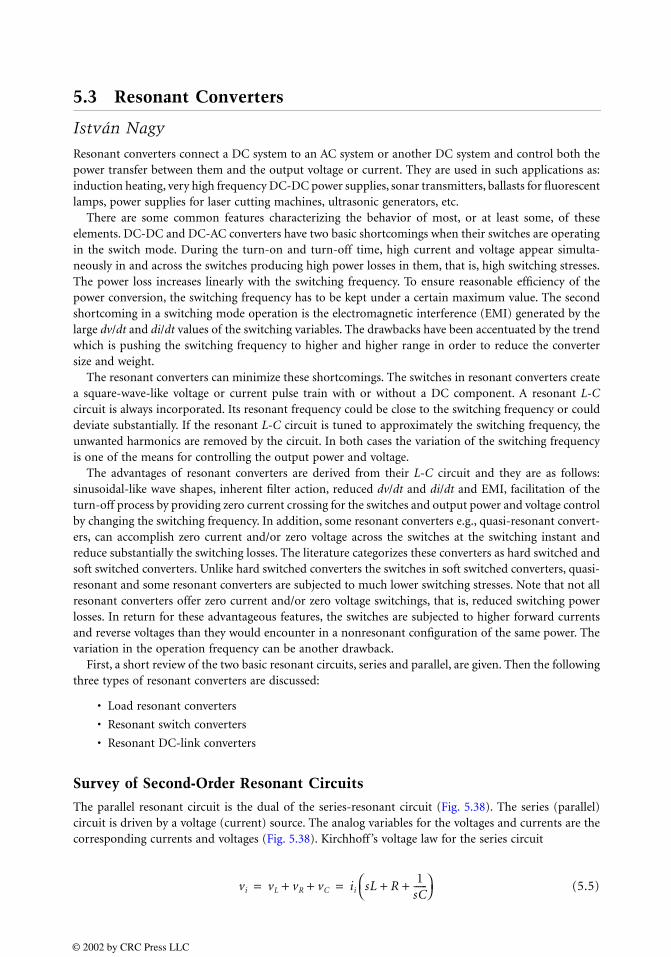
5.3 Resonant Converters
István Nagy
Resonant converters connect a DC system to an AC system or another DC system and control both thepower transfer between them and the output voltage or current. They are used in such applications as:induction heating, very high frequency DC-DC power supplies, sonar transmitters, ballasts for fluorescentlamps, power supplies for laser cutting machines, ultrasonic generators, etc.
There are some common features characterizing the behavior of most, or at least some, of theseelements. DC-DC and DC-AC converters have two basic shortcomings when their switches are operatingin the switch mode. During the turn-on and turn-off time, high current and voltage appear simulta-neously in and across the switches producing high power losses in them, that is, high switching stresses.The power loss increases linearly with the switching frequency. To ensure reasonable efficiency of thepower conversion, the switching frequency has to be kept under a certain maximum value. The secondshortcoming in a switching mode operation is the electromagnetic interference (EMI) generated by thelarge dv/dt and di/dt values of the switching variables. The drawbacks have been accentuated by the trendwhich is pushing the switching frequency to higher and higher range in order to reduce the convertersize and weight.
The resonant converters can minimize these shortcomings. The switches in resonant converters createa square-wave-like voltage or current pulse train with or without a DC component. A resonant L-Ccircuit is always incorporated. Its resonant frequency could be close to the switching frequency or coulddeviate substantially. If the resonant L-C circuit is tuned to approximately the switching frequency, theunwanted harmonics are removed by the circuit. In both cases the variation of the switching frequencyis one of the means for controlling the output power and voltage.
The advantages of resonant converters are derived from their L-C circuit and they are as follows:sinusoidal-like wave shapes, inherent filter action, reduced dv/dt and di/dt and EMI, facilitation of theturn-off process by providing zero current crossing for the switches and output power and voltage controlby changing the switching frequency. In addition, some resonant converters e.g., quasi-resonant convert-ers, can accomplish zero current and/or zero voltage across the switches at the switching instant andreduce substantially the switching losses. The literature categorizes these converters as hard switched andsoft switched converters. Unlike hard switched converters the switches in soft switched converters, quasi-resonant and some resonant converters are subjected to much lower switching stresses. Note that not allresonant converters offer zero current and/or zero voltage switchings, that is, reduced switching powerlosses. In return for these advantageous features, the switches are subjected to higher forward currentsand reverse voltages than they would encounter in a nonresonant configuration of the same power. Thevariation in the operation frequency can be another drawback.
First, a short review of the two basic resonant circuits, series and parallel, are given. Then the followingthree types of resonant converters are discussed:
• Load resonant converters
• Resonant switch converters
• Resonant DC-link converters
Survey of Second-Order Resonant Circuits
The parallel resonant circuit is the dual of the series-resonant circuit (Fig. 5.38). The series (parallel)circuit is driven by a voltage (current) source. The analog variables for the voltages and currents are thecorresponding currents and voltages (Fig. 5.38). Kirchhoff ’s voltage law for the series circuit
(5.5)vi vL vR vC+ + ii sL R1
sC------+ +
= =
© 2002 by CRC Press LLC

and Kirchhoff ’s current law for the parallel circuit
(5.6)
have to be used. The analog parameters for the impedances are the corresponding admittances (Fig. 5.38).The input current for the series circuit is
(5.7)
and the input voltage for the parallel circuit is
(5.8)
where the input admittance is
(5.9)
FIGURE 5.38 Dual circuits.
vi
+
− Ys(s)
C
vc
+−
R
+
+ +
−
−
vT
Zp(s)
vR
ii
ii L
iL iC iR
viC R
Series Parallel Series Parallel
vi ii
vL iL
vR iR
vC iC
ii vi
sL1sL
R
1
Cs
Z(s) Y(s)
Cs
1R
−
L
ii iL iR iC+ + vi1sL----- 1
R--- sC+ +
= =
ii Ys s( )vi1
Zs s( )------------vi= =
vi Zp s( )ii=
Ys s( ) 1R---
2ξsTs
T 2s2 2ξsTs 1+ +----------------------------------------=
© 2002 by CRC Press LLC

and the input impedance is
(5.10)
The time constant and the damping factor ξ together with some other parameters are given in Table 5.1.ξ must be smaller than unity in Eqs. (5.9) and (5.10) to have complex roots in the denominators, thatis, to obtain an oscillatory response.
When vi is a unit step function, vi(s) = 1/s, the time response of the voltage across R in the seriesresonance circuit from Eqs. (5.7) and (5.9) is
(5.11)
or for ξs = 0
(5.11a)
that is, the response is a damped, or for ξs = 0 undamped, sinusoidal function.When the current changes as a step function in the parallel circuit, Rii(s) = 1/s, the expression for the
voltage response vi is given by the right side of Eq. 5.11, as well, since RYs = Zp /R. Of course, now ξs hasto be replaced by ξp. The time function f(t/T) for various damping factors ξ is shown in Fig. 5.39.
Assuming sinusoidal input variables, the frequency response for series circuit is
(5.12)
and for parallel circuit is
(5.13)
TABLE 5.1 Parameters
Series Parallel
Time constantResonant angular
frequencyDamping factor
Characteristic impedance
Damped resonant angular frequency
Quality factor
T LC=ω0 2πf0
1T---= =
ξs12-- R
ω0L--------- 1
2--ω0CR= = ξp
12--
ω0LR
--------- 12-- 1
ω0CR--------------= =
Z0 L/C=
ωd ω0 1 ξs2–= ωd ω0 1 ξp
2–=
Qs1
2ξs
-------= Qp1
2ξp
--------=
Zp s( ) R2ξpTs
T 2s2 2ξpTs 1+ +----------------------------------------=
Rii t( ) 2ξsT1
T 1 ξs2–
---------------------- eξst/T–
( 1 ξs2– )t/Tsin=
2ξsTf(t/T)=
ii t( ) 1ω0L--------- ω0tsin=
Rii
νi
------- RYs jν( ) 11 jQs ν 1/ν–( )+---------------------------------------- 1
Ds ν( )--------------= = =
νi
Ri i
------- 1R---Zp jν( ) 1
1 jQp ν 1/ν–( )+----------------------------------------- 1
Dp ν( )--------------= = =
© 2002 by CRC Press LLC

where
Both circuits are purely resistive at resonance: when ν = 1.The plot of the amplitude and phase of the right side of Eqs. (5.12) and (5.13) as a function of ν are
shown in Fig. 5.40. The voltage across R and its power can be changed by varying ν. When Q is high, asmall change in ν can produce a large variation in the output.
The voltage across the energy storage components, for instance, across L in the series circuit, is
(5.14)
and the currents in the energy storage components, for instance, in L in the parallel circuit, is
(5.15)
The voltages (currents) of the energy storage components in series (parallel) resonant circuits at ν = 1is Q times as high as the input voltage (current) (Table 5.2). If Q = 10 the capacitor or inductor voltage(current) is ten times the source voltage (current).
The value of L and C and their power rating is tied to the quality factor. The higher the value of Q,the better the filter action, that is, the attenuation of the harmonics is better and it is easier to controlthe output voltage and power by a small change in the switching frequency. The definition of Q is
(5.16)
Using this definition, the expressions for Q are given in Table 5.2 where Ip and Vp are the peak currentin the inductor and peak voltage across the capacitor, respectively. For a given output power, the energy
FIGURE 5.39 Time response of f (t/T). (T = 1).
ξ=0.01
ξ=0.025
ξ=0.05
ξ=0.1
ξ=0.25
0-1
-0.8
-0.6
-0.4
-0.2
0.2
0.4
0.6
0.8
1
0
2 4 6 8 10
t/T
f(t/T)
ν ω/ω0.=
vi Ri i=
νL
νi
-----jνQs
Ns ν( )--------------=
iL
ii
-----Qp
jνNp ν( )--------------------=
Q2π Peak stored energy×
Energy dissipated per cycle----------------------------------------------------------------=
© 2002 by CRC Press LLC

TABLE 5.2 Resonance, ω = ωo
Series Parallel
FIGURE 5.40 Frequency response of Amplitude (a), phase (b).
vc
vi
---- jQs–= i C
i i
----- jQp=
vL
vi
---- jQs= i L
i i
---- j– Qp=
Qs
2π 12--LIP
2( )12--RIP
2( ) 1f0
--------------------------= Qp
2π 12--CV P
2( )
12--
VP2
R-------
1f0
---
---------------------------=
10-1 100 101
10-1 100 101
0
0.2
0.4
0.6
0.8
1.0
0
-50
50
100
100
Q=2
Q=5
Q=10
Q=20
Q=50
Q=50
Q=20
Q=10Q=5
Q=2
a.
b.
ϕ
R Y_
( jv)
υ
υ
RY( jν)[ ] .
© 2002 by CRC Press LLC
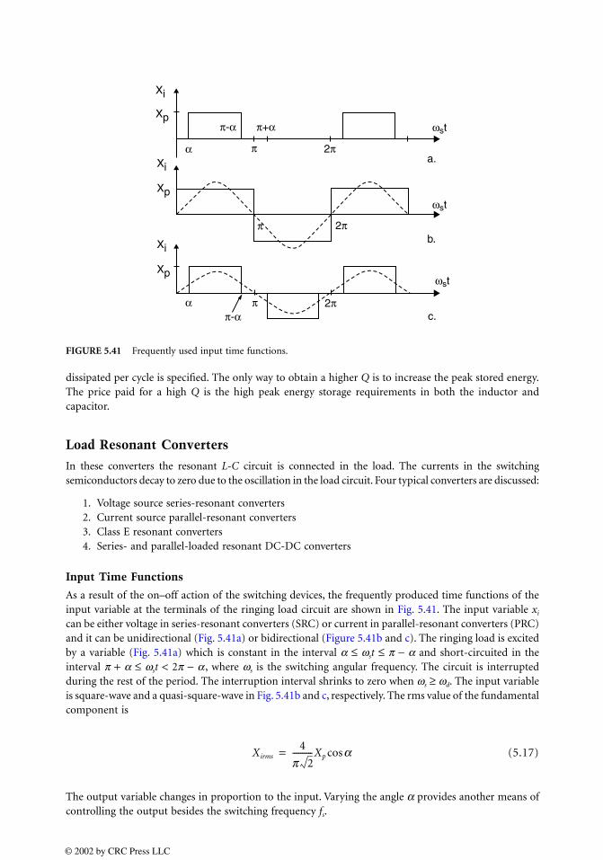
dissipated per cycle is specified. The only way to obtain a higher Q is to increase the peak stored energy.The price paid for a high Q is the high peak energy storage requirements in both the inductor andcapacitor.
Load Resonant Converters
In these converters the resonant L-C circuit is connected in the load. The currents in the switchingsemiconductors decay to zero due to the oscillation in the load circuit. Four typical converters are discussed:
1. Voltage source series-resonant converters2. Current source parallel-resonant converters3. Class E resonant converters4. Series- and parallel-loaded resonant DC-DC converters
Input Time Functions
As a result of the on–off action of the switching devices, the frequently produced time functions of theinput variable at the terminals of the ringing load circuit are shown in Fig. 5.41. The input variable xi
can be either voltage in series-resonant converters (SRC) or current in parallel-resonant converters (PRC)and it can be unidirectional (Fig. 5.41a) or bidirectional (Figure 5.41b and c). The ringing load is excitedby a variable (Fig. 5.41a) which is constant in the interval α ≤ ωst ≤ π − α and short-circuited in theinterval π + α ≤ ωst < 2π − α , where ωs is the switching angular frequency. The circuit is interruptedduring the rest of the period. The interruption interval shrinks to zero when ωs ≥ ωd. The input variableis square-wave and a quasi-square-wave in Fig. 5.41b and c, respectively. The rms value of the fundamentalcomponent is
(5.17)
The output variable changes in proportion to the input. Varying the angle α provides another means ofcontrolling the output besides the switching frequency fs.
FIGURE 5.41 Frequently used input time functions.
a.
b.
c.
α
α
π
π
π
ωst
ωst
ωst
π+απ-α
π-α
2π
2π
2π
Xi
Xp
Xi
Xp
Xi
Xp
Xirms4
π 2----------Xp αcos=
© 2002 by CRC Press LLC
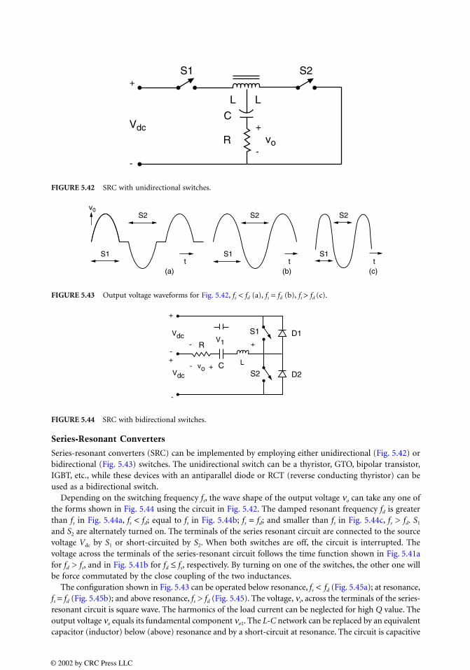
Series-Resonant Converters
Series-resonant converters (SRC) can be implemented by employing either unidirectional (Fig. 5.42) orbidirectional (Fig. 5.43) switches. The unidirectional switch can be a thyristor, GTO, bipolar transistor,IGBT, etc., while these devices with an antiparallel diode or RCT (reverse conducting thyristor) can beused as a bidirectional switch.
Depending on the switching frequency fs, the wave shape of the output voltage νo can take any one ofthe forms shown in Fig. 5.44 using the circuit in Fig. 5.42. The damped resonant frequency fd is greaterthan fs in Fig. 5.44a, fs < fd; equal to fs in Fig. 5.44b; fs = fd; and smaller than fs in Fig. 5.44c, fs > fd. S1
and S2 are alternately turned on. The terminals of the series resonant circuit are connected to the sourcevoltage Vdc by S1 or short-circuited by S2. When both switches are off, the circuit is interrupted. Thevoltage across the terminals of the series-resonant circuit follows the time function shown in Fig. 5.41afor fd > fs, and in Fig. 5.41b for fd ≤ fs, respectively. By turning on one of the switches, the other one willbe force commutated by the close coupling of the two inductances.
The configuration shown in Fig. 5.43 can be operated below resonance, fs < fd (Fig. 5.45a); at resonance,fs = fd (Fig. 5.45b); and above resonance, fs > fd (Fig. 5.45). The voltage, νi, across the terminals of the series-resonant circuit is square wave. The harmonics of the load current can be neglected for high Q value. Theoutput voltage νo equals its fundamental component νo1. The L-C network can be replaced by an equivalentcapacitor (inductor) below (above) resonance and by a short-circuit at resonance. The circuit is capacitive
FIGURE 5.42 SRC with unidirectional switches.
FIGURE 5.43 Output voltage waveforms for Fig. 5.42, fs < fd (a), fs = fd (b), fs > fd (c).
FIGURE 5.44 SRC with bidirectional switches.
+
+
--
Vdcvo
S1 S2
C
R
L L
(a) (b) (c)
S1 S1 S1
S2 S2 S2
t t t
v0
+
+
++-
-
-
- voVdc
Vdc V1R
S1
S2 D2
D1
C L
© 2002 by CRC Press LLC
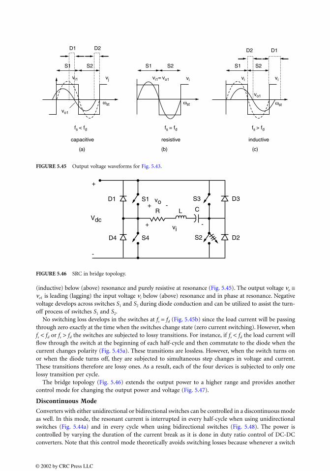
(inductive) below (above) resonance and purely resistive at resonance (Fig. 5.45). The output voltage νo ≅νo1 is leading (lagging) the input voltage νi below (above) resonance and in phase at resonance. Negativevoltage develops across switches S1 and S2 during diode conduction and can be utilized to assist the turn-off process of switches S1 and S2.
No switching loss develops in the switches at fs = fd (Fig. 5.45b) since the load current will be passingthrough zero exactly at the time when the switches change state (zero current switching). However, whenfs < fd or fs > fd the switches are subjected to lossy transitions. For instance, if fs < fd the load current willflow through the switch at the beginning of each half-cycle and then commutate to the diode when thecurrent changes polarity (Fig. 5.45a). These transitions are lossless. However, when the switch turns onor when the diode turns off, they are subjected to simultaneous step changes in voltage and current.These transitions therefore are lossy ones. As a result, each of the four devices is subjected to only onelossy transition per cycle.
The bridge topology (Fig. 5.46) extends the output power to a higher range and provides anothercontrol mode for changing the output power and voltage (Fig. 5.47).
Discontinuous Mode
Converters with either unidirectional or bidirectional switches can be controlled in a discontinuous modeas well. In this mode, the resonant current is interrupted in every half-cycle when using unidirectionalswitches (Fig. 5.44a) and in every cycle when using bidirectional switches (Fig. 5.48). The power iscontrolled by varying the duration of the current break as it is done in duty ratio control of DC-DCconverters. Note that this control mode theoretically avoids switching losses because whenever a switch
FIGURE 5.45 Output voltage waveforms for Fig. 5.43.
FIGURE 5.46 SRC in bridge topology.
D1
S1 S1 S1 S2S2S2
D2 D2 D1
vi1 vj vi vi1= vo1 vivi
vo1
vo1
ωst ωst ωst
fs < fd fs = fd fs > fd
capacitive resistive inductive
(a) (b) (c)
D1
D4 S4
S1 S3 D3
D2S2
R L C
+
+
-
-
-
+
vi
vo
Vdc
© 2002 by CRC Press LLC
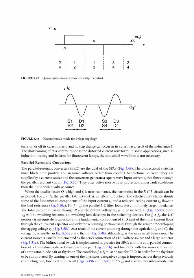
turns on or off its current is zero and no step change can occur in its current as a result of the inductance L.The shortcoming of this control mode is the distorted current waveform. In some applications, such asinduction heating and ballasts for fluorescent lamps, the sinusoidal waveform is not necessary.
Parallel-Resonant Converters
The parallel-resonant converters (PRC) are the dual of the SRCs (Fig. 5.49). The bidirectional switchesmust block both positive and negative voltages rather than conduct bidirectional current. They aresupplied by a current source and the converters generate a square wave input current ii that flows throughthe parallel resonant circuit (Fig. 5.50). They offer better short-circuit protection under fault conditionsthan the SRCs with a voltage source.
When the quality factor Q is high and fs is near resonance, the harmonics in the R-C-L circuit can beneglected. For fs < fd, the parallel L-C network is, in effect, inductive. The effective inductance shuntssome of the fundamental components of the input current ii1 and a reduced leading current ii1 flows inthe load resistance (Fig. 5.50a). For fs = fd, the parallel L-C filter looks like an infinitely large impedance.The total current ii1 passes through R and the output voltage νo1 is in phase with ii1 (Fig. 5.50b). Sinceνo1 = 0 at switching instants, no switching loss develops in the switching devices. For fs > fd, the L-Cnetwork is an equivalent capacitor at the fundamental component of ii1. A part of the input current flowsthrough the equivalent capacitor and only the remaining portion passes through the resistor R developingthe lagging voltage νo1 (Fig. 5.50c). As a result of the current shunting through the equivalent Le and Ce, thevoltage νo1 is smaller in Fig. 5.50a and c than in Fig. 5.50b, although ii1 is the same in all three cases. Thecurrent source is usually implemented by the series connection of a DC voltage source and a large inductor(Fig. 5.51a). The bidirectional switch is implemented in practice for SRCs with the anti-parallel connec-tion of a transistor-diode or thyristor–diode pair (Fig. 5.51b) and for PRCs with the series connectionof a transistor-diode pair or thyristor. The condition fs > fd must be met for PRCs in order for the thyristorto be commutated. By turning on one of the thyristors, a negative voltage is imposed across the previouslyconducting one, forcing it to turn off (Figs. 5.49b and 5.50c). If fs > fd and a series transistor–diode pair
FIGURE 5.47 Quasi-square-wave voltage for output control.
FIGURE 5.48 Discontinuous mode for bridge topology.
2 1 1 3 24 2 3 4 4
α
π 2πωst
vi
S1S2
D1D2
S3S4
D3D4
ωst
io
© 2002 by CRC Press LLC
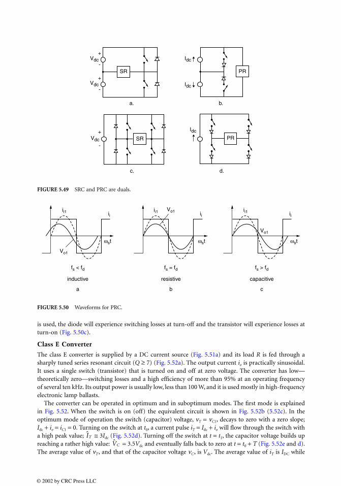
is used, the diode will experience switching losses at turn-off and the transistor will experience losses atturn-on (Fig. 5.50c).
Class E Converter
The class E converter is supplied by a DC current source (Fig. 5.51a) and its load R is fed through asharply tuned series resonant circuit (Q ≥ 7) (Fig. 5.52a). The output current io is practically sinusoidal.It uses a single switch (transistor) that is turned on and off at zero voltage. The converter has low—theoretically zero—switching losses and a high efficiency of more than 95% at an operating frequencyof several ten kHz. Its output power is usually low, less than 100 W, and it is used mostly in high-frequencyelectronic lamp ballasts.
The converter can be operated in optimum and in suboptimum modes. The first mode is explainedin Fig. 5.52. When the switch is on (off) the equivalent circuit is shown in Fig. 5.52b (5.52c). In theoptimum mode of operation the switch (capacitor) voltage, νT = νC1, decays to zero with a zero slope;Idc + io = iC1 = 0. Turning on the switch at t0, a current pulse iT = Idc + io will flow through the switch witha high peak value; ≅ 3Idc (Fig. 5.52d). Turning off the switch at t = t1, the capacitor voltage builds upreaching a rather high value: = 3.5Vdc and eventually falls back to zero at t = t0 + T (Fig. 5.52e and d).The average value of νT, and that of the capacitor voltage νC, is Vdc. The average value of iT is IDC while
FIGURE 5.49 SRC and PRC are duals.
FIGURE 5.50 Waveforms for PRC.
a. b.
c. d.
PR
PR
SR
SR
+
-
-
-
+
+
Vdc Idc
Idc
Idc
Vdc
Vdc
ii1 ii
Vo1
ωst
ii1 iiVo1
ωst
iiii1
Vo1
ωst
fs < fd
inductive
a
fs = fd
resistive
b
fs > fd
capacitive
c
IT
VC
© 2002 by CRC Press LLC
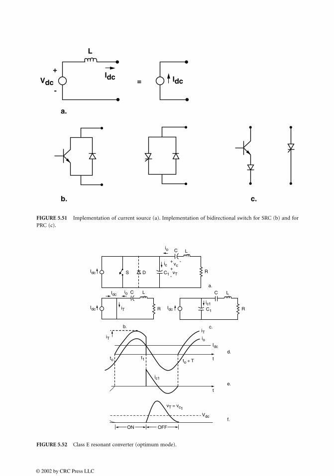
FIGURE 5.51 Implementation of current source (a). Implementation of bidirectional switch for SRC (b) and forPRC (c).
FIGURE 5.52 Class E resonant converter (optimum mode).
L
Idc IdcVdc =
a.
b. c.
+
-
D R
RR
S C1
C1
C
C
C
L
LL
vT
iT
iT
iT
vcic
ic1
ic1
io
io
io
to to + T t
t
f.
t1
Idc
Idc
Idc
Idc
Vdc
vT = vc1
Idc
+
+
-
-
a.
b. c.
d.
e.
ON OFF
© 2002 by CRC Press LLC
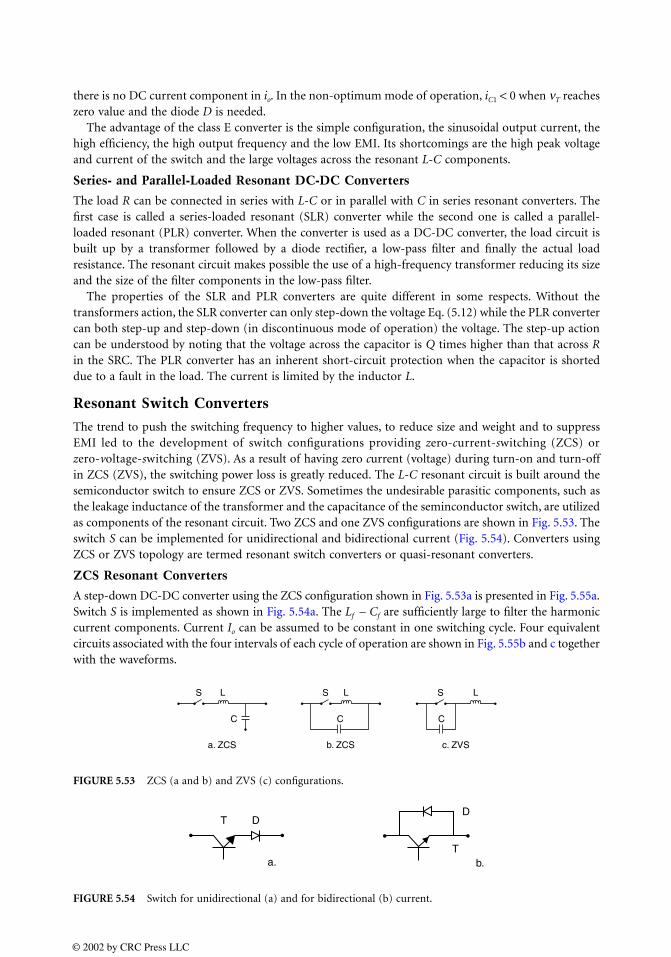
there is no DC current component in io. In the non-optimum mode of operation, iC1 < 0 when νT reacheszero value and the diode D is needed.
The advantage of the class E converter is the simple configuration, the sinusoidal output current, thehigh efficiency, the high output frequency and the low EMI. Its shortcomings are the high peak voltageand current of the switch and the large voltages across the resonant L-C components.
Series- and Parallel-Loaded Resonant DC-DC Converters
The load R can be connected in series with L-C or in parallel with C in series resonant converters. Thefirst case is called a series-loaded resonant (SLR) converter while the second one is called a parallel-loaded resonant (PLR) converter. When the converter is used as a DC-DC converter, the load circuit isbuilt up by a transformer followed by a diode rectifier, a low-pass filter and finally the actual loadresistance. The resonant circuit makes possible the use of a high-frequency transformer reducing its sizeand the size of the filter components in the low-pass filter.
The properties of the SLR and PLR converters are quite different in some respects. Without thetransformers action, the SLR converter can only step-down the voltage Eq. (5.12) while the PLR convertercan both step-up and step-down (in discontinuous mode of operation) the voltage. The step-up actioncan be understood by noting that the voltage across the capacitor is Q times higher than that across Rin the SRC. The PLR converter has an inherent short-circuit protection when the capacitor is shorteddue to a fault in the load. The current is limited by the inductor L.
Resonant Switch Converters
The trend to push the switching frequency to higher values, to reduce size and weight and to suppressEMI led to the development of switch configurations providing zero-current-switching (ZCS) orzero-voltage-switching (ZVS). As a result of having zero current (voltage) during turn-on and turn-offin ZCS (ZVS), the switching power loss is greatly reduced. The L-C resonant circuit is built around thesemiconductor switch to ensure ZCS or ZVS. Sometimes the undesirable parasitic components, such asthe leakage inductance of the transformer and the capacitance of the seminconductor switch, are utilizedas components of the resonant circuit. Two ZCS and one ZVS configurations are shown in Fig. 5.53. Theswitch S can be implemented for unidirectional and bidirectional current (Fig. 5.54). Converters usingZCS or ZVS topology are termed resonant switch converters or quasi-resonant converters.
ZCS Resonant Converters
A step-down DC-DC converter using the ZCS configuration shown in Fig. 5.53a is presented in Fig. 5.55a.Switch S is implemented as shown in Fig. 5.54a. The Lf – Cf are sufficiently large to filter the harmoniccurrent components. Current Io can be assumed to be constant in one switching cycle. Four equivalentcircuits associated with the four intervals of each cycle of operation are shown in Fig. 5.55b and c togetherwith the waveforms.
FIGURE 5.53 ZCS (a and b) and ZVS (c) configurations.
FIGURE 5.54 Switch for unidirectional (a) and for bidirectional (b) current.
S L S SL L
C C C
a. ZCS b. ZCS c. ZVS
T
T
DD
a. b.
© 2002 by CRC Press LLC
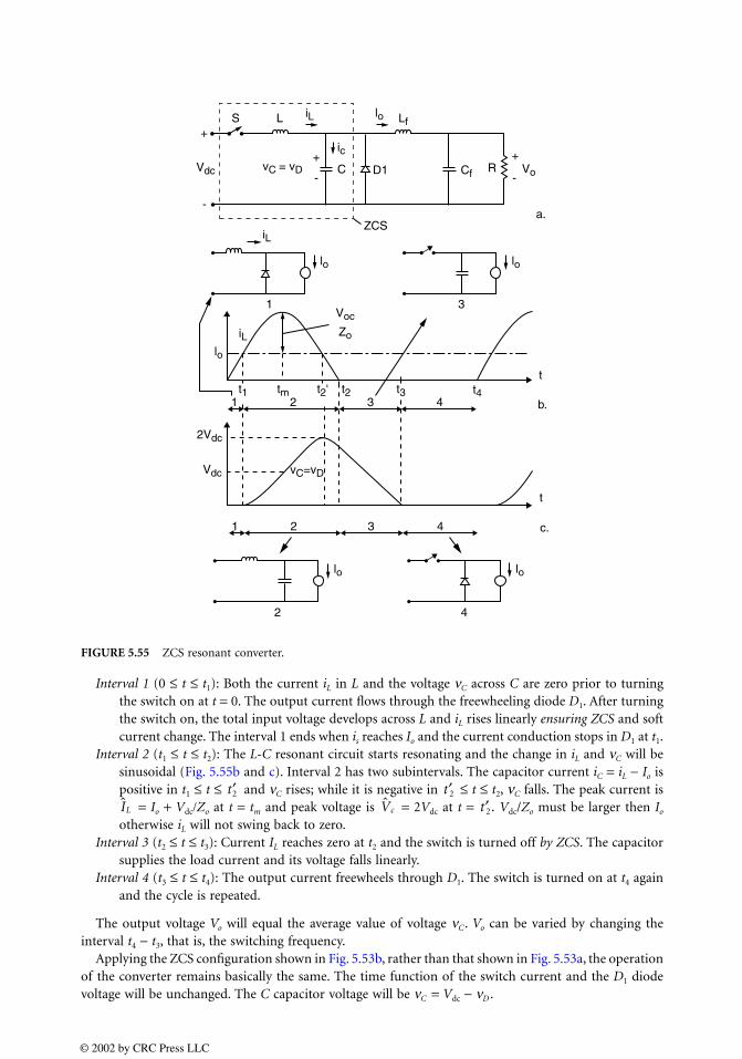
Interval 1 (0 ≤ t ≤ t1): Both the current iL in L and the voltage νC across C are zero prior to turningthe switch on at t = 0. The output current flows through the freewheeling diode D1. After turningthe switch on, the total input voltage develops across L and iL rises linearly ensuring ZCS and softcurrent change. The interval 1 ends when is reaches Io and the current conduction stops in D1 at t1.
Interval 2 (t1 ≤ t ≤ t2): The L-C resonant circuit starts resonating and the change in iL and νC will besinusoidal (Fig. 5.55b and c). Interval 2 has two subintervals. The capacitor current iC = iL − Io ispositive in t1 ≤ t ≤ and νC rises; while it is negative in ≤ t ≤ t2, νC falls. The peak current is
= Io + Vdc/Zo at t = tm and peak voltage is = 2Vdc at t = Vdc/Zo must be larger then Io
otherwise iL will not swing back to zero.Interval 3 (t2 ≤ t ≤ t3): Current IL reaches zero at t2 and the switch is turned off by ZCS. The capacitor
supplies the load current and its voltage falls linearly.Interval 4 (t3 ≤ t ≤ t4): The output current freewheels through D1. The switch is turned on at t4 again
and the cycle is repeated.
The output voltage Vo will equal the average value of voltage νC. Vo can be varied by changing theinterval t4 − t3, that is, the switching frequency.
Applying the ZCS configuration shown in Fig. 5.53b, rather than that shown in Fig. 5.53a, the operationof the converter remains basically the same. The time function of the switch current and the D1 diodevoltage will be unchanged. The C capacitor voltage will be νC = Vdc − νD .
FIGURE 5.55 ZCS resonant converter.
S L
Vdc
2Vdc
Vdc vC=vD
Voc1
1 2 3 4
1 2
2
3 4
4
3
a.
b.
c.
Zo
t4t3t2tmt1 t2't
t
iL
iL
lo
lo
lo lo
lo
Cf VovC = vD
ic
iL lo Lf
C+
+
+
- -
-
ZCS
D1 R
t′2 t′2IL Vc t′2.
© 2002 by CRC Press LLC
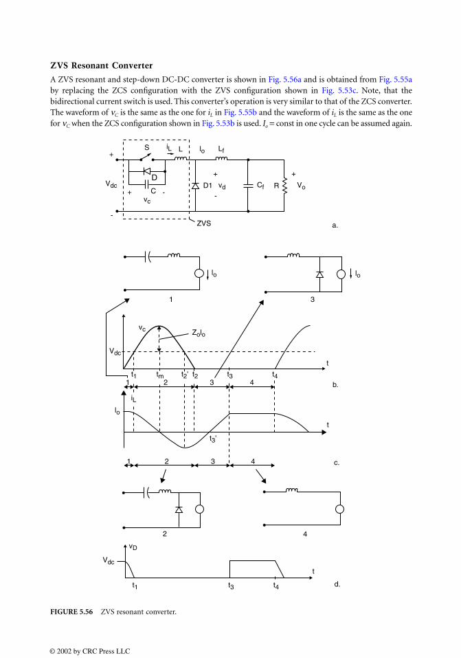
ZVS Resonant Converter
A ZVS resonant and step-down DC-DC converter is shown in Fig. 5.56a and is obtained from Fig. 5.55aby replacing the ZCS configuration with the ZVS configuration shown in Fig. 5.53c. Note, that thebidirectional current switch is used. This converter’s operation is very similar to that of the ZCS converter.The waveform of νC is the same as the one for iL in Fig. 5.55b and the waveform of iL is the same as the onefor νC when the ZCS configuration shown in Fig. 5.53b is used. Io = const in one cycle can be assumed again.
FIGURE 5.56 ZVS resonant converter.
S L
D
CD1
ZVS
RVdc
Vdc
Vdc
vD
vc
vc
t1 t2 t3 t4
t1 t3 t4
tm t2'
t3'
vd Cf Vo
lo
lo
lo
Zolo
lo
LfiL
iL
1 3
a.
t
t
b.
c.
2 4
d.
t
1 2 3 4
1 2 3 4
+
+
+ +
-
- -
© 2002 by CRC Press LLC

Interval 1 (0 ≤ t ≤ t1): S is turned off at t = 0. The constant iL = Io current starts passing through thecapacitor C. Its voltage νC rises linearly from zero to Vdc. ZVS occurs.
Interval 2 (t1 ≤ t ≤ t2): Diode D1 turns on at t1. The L-C circuit starts resonating through D1 and thesource. Both νC and iL are changing sinusoidally. When iL drops at zero νC reaches its peak value:
= Vdc + ZoIo. The voltage νC reaches zero at t2. The load current must be high enough so thatZoIo > Vdc ; otherwise νC will not reach zero and the switch will have to be turned on at nonzerovoltage.
Interval 3 (t2 ≤ t ≤ t3): Diode D turns on. It clamps νC to zero and conducts iL. The gate signal isreapplied to the switch. Vdc develops across L and iL increases linearly up to Io, which is reachedat t3. Prior to that, the current iL changes its polarity at and S begins to conduct it.
Interval 4 (t3 ≤ t ≤ t4): Freewheeling diode D1 turns off at t3. It is a soft transition because of the smallnegative slope of the current iD. Current Io flows through S at t4 when S is turned off and the nextcycle begins.
Diode voltage νD develops across D1 only in intervals 1 and 4 (Fig. 5.56d). Its average value is equalto Vo which can be varied by interval 4, or in other words, by the switching frequency.
Summary and Comparison of ZCS and ZVS Converters
The main properties of ZCS and ZVS are highlighted as follows:
• The switch turn-on and turn-off occurs at zero current or at zero voltage which significantlyreduces the switching losses.
• Sudden current and voltage changes in the switch are avoided in ZCS and in ZVS, respectively.The di/dt and dv/dt values are rather small. EMI is reduced.
• In the ZCS, the peak current Io + Vdc /Zo conducted by S must be more than twice as high as themaximum of the load current Io.
• In the ZVS, the switch must withstand the forward voltage Vdc + ZoIo and ZoIo must exceed Vdc.
• The output voltage can be varied by the switching frequency.
• The internal capacitances of the switch are discharged during turn-on in ZCS which can producesignificant switching loss at high switching frequency. No such loss occurs in ZVS.
Two-Quadrant ZVS Resonant Converters
One drawback in the ZVS converter, shown in Fig. 5.56, is that the switch peak forward voltage issignificantly higher than the supply voltage. This drawback does not appear in the two-quadrant ZVSresonant converter where the switch voltage is clamped at the input voltage. In addition, this techniquecan be extended to the single phase and the three-phase DC-to-AC converter to supply an inductive load.
The basic principle will be presented by means of the DC-DC stepdown converter shown in Fig. 5.57a.Two switches, two diodes and two resonant capacitors C1 = C2 = C are used. The voltage Vo can be assumedto be constant in one switching period because Cf is large. The current iL must fluctuate in large scaleand must take both positive and negative values in one switching cycle. To achieve this operation L mustbe rather small. One cycle consists of six intervals.
Interval 1. S1 is on. The inductor voltage is νL = Vdc − Vo. iL rises linearly from zero.Interval 2. S1 is turned off at t1. None of the four semiconductors conducts. The resonant circuit
consisting of L and the two capacitors connected in parallel is ringing through the source and theload. Now the impedance Zo = is high (C is small) and the peak current will be small.The voltage across C2 approximately changes linearly and reaches zero at t2. As a result of C1 thevoltage across S1 changes slowly from zero.
Interval 3. D2 conducts iL. The inductor voltage νL is −Vo. iL is reduced linearly to zero at t3. S2 is turnedon in this interval when its voltage is zero.
Interval 4. S2 begins to conduct, νL is still − Vo and iL increases linearly in a negative direction.
VC
t′3
2L/C
© 2002 by CRC Press LLC
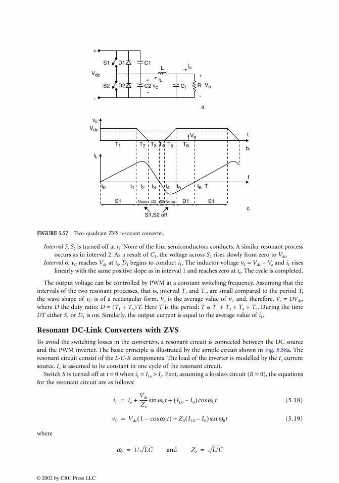
Interval 5. S2 is turned off at t4. None of the four semiconductors conducts. A similar resonant processoccurs as in interval 2. As a result of C2, the voltage across S2 rises slowly from zero to Vdc.
Interval 6. νC reaches Vdc at t5. D1 begins to conduct iL. The inductor voltage νL = Vdc − Vo and iL riseslinearly with the same positive slope as in interval 1 and reaches zero at t6. The cycle is completed.
The output voltage can be controlled by PWM at a constant switching frequency. Assuming that theintervals of the two resonant processes, that is, interval T2 and T5, are small compared to the period T,the wave shape of νC is of a rectangular form. Vo is the average value of νC and, therefore, Vo = DVdc,where D the duty ratio: D = (T1 + T6)/T. Here T is the period: T ≅ T1 + T3 + T4 + T6. During the timeDT either S1 or D1 is on. Similarly, the output current is equal to the average value of iL.
Resonant DC-Link Converters with ZVS
To avoid the switching losses in the converters, a resonant circuit is connected between the DC sourceand the PWM inverter. The basic principle is illustrated by the simple circuit shown in Fig. 5.58a. Theresonant circuit consist of the L-C-R components. The load of the inverter is modelled by the Io currentsource. Io is assumed to be constant in one cycle of the resonant circuit.
Switch S is turned off at t = 0 when iL = ILo > Io. First, assuming a lossless circuit (R = 0), the equationsfor the resonant circuit are as follows:
(5.18)
(5.19)
where
FIGURE 5.57 Two-quadrant ZVS resonant converter.
S1
+
--
-
++
S2
D1
D2
C1
C2
L
R
Vdc
Vdc
T1
S1
S1,S2 off
S1D1D2 S2
T2 T3 T4 T5
t1t0 t2 t3 t4 t5 t6=T
T6
vc
vc
Vo
Vo
lo
Cf
a.
b.
iL
iL
t
t
c.None None
iL Io
Vdc
Zo
------- ω0t IL0 I0–( ) ω0tcos+sin+=
vC Vdc 1 ω0tcos–( ) Z0 IL0 I0–( ) ω0tsin+=
ωo 1/ LC and Zo L/C= =
© 2002 by CRC Press LLC
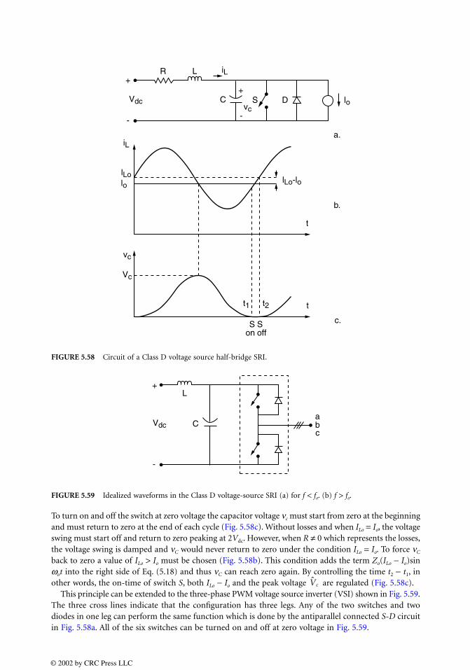
To turn on and off the switch at zero voltage the capacitor voltage νc must start from zero at the beginningand must return to zero at the end of each cycle (Fig. 5.58c). Without losses and when ILo = Io, the voltageswing must start off and return to zero peaking at 2Vdc. However, when R ≠ 0 which represents the losses,the voltage swing is damped and νC would never return to zero under the condition ILo = Io. To force νC
back to zero a value of ILo > Io must be chosen (Fig. 5.58b). This condition adds the term Zo(ILo − Io)sinωot into the right side of Eq. (5.18) and thus νC can reach zero again. By controlling the time t2 − t1, inother words, the on-time of switch S, both ILo − Io and the peak voltage are regulated (Fig. 5.58c).
This principle can be extended to the three-phase PWM voltage source inverter (VSI) shown in Fig. 5.59.The three cross lines indicate that the configuration has three legs. Any of the two switches and twodiodes in one leg can perform the same function which is done by the antiparallel connected S-D circuitin Fig. 5.58a. All of the six switches can be turned on and off at zero voltage in Fig. 5.59.
FIGURE 5.58 Circuit of a Class D voltage source half-bridge SRI.
FIGURE 5.59 Idealized waveforms in the Class D voltage-source SRI (a) for f < fo. (b) f > fo.
R L
C S D
a.
b.
c.
t
t
Vdcvc
vc
t1
S S
t2
Vc
iL
iL
lLolLo-lolo
lo
on off
++
- -
L
C
+
-
Vdcabc
Vc
© 2002 by CRC Press LLC
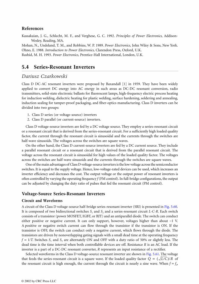
References
Kassakaian, J. G., Schlecht, M. F., and Verghese, G. C. 1992. Principles of Power Electronics, Addison-Wesley, Reading, MA.
Mohan, N., Undeland, T. M., and Robbins, W. P. 1989. Power Electronics, John Wiley & Sons, New York.Ohno, E. 1988. Introduction to Power Electronics, Clarendon Press, Oxford, U.K.Rashid, M. H. 1993. Power Electronics, Prentice-Hall International, London, U.K.
5.4 Series-Resonant Inverters
Dariusz Czarkowski
Class D DC-AC resonant inverters were proposed by Baxandall [1] in 1959. They have been widelyapplied to convert DC energy into AC energy in such areas as DC-DC resonant conversion, radiotransmitters, solid-state electronic ballasts for fluorescent lamps, high-frequency electric process heatingfor induction welding, dielectric heating for plastic welding, surface hardening, soldering and annealing,induction sealing for tamper-proof packaging, and fiber-optics manufacturing. Class D inverters can bedivided into two groups:
1. Class D series (or voltage-source) inverters 2. Class D parallel (or current-source) inverters.
Class D voltage-source inverters are fed by a DC voltage source. They employ a series-resonant circuitor a resonant circuit that is derived from the series-resonant circuit. For a sufficiently high loaded qualityfactor, the current through the resonant circuit is sinusoidal and the currents through the switches arehalf-wave sinusoids. The voltages across the switches are square waves.
On the other hand, the Class D current-source inverters are fed by a DC current source. They includea parallel resonant circuit or a resonant circuit that is derived from the parallel resonant circuit. Thevoltage across the resonant circuit is sinusoidal for high values of the loaded quality factor. The voltagesacross the switches are half-wave sinusoids and the currents through the switches are square waves.
One of the main advantages of Class D voltage-source inverters is the low voltage across the semiconductorswitches. It is equal to the supply voltage. Hence, low-voltage-rated devices can be used, which increases aninverter efficiency and decreases the cost. The output voltage or the output power of resonant inverters isoften controlled by varying the operating frequency f (FM control). In full-bridge configurations, the outputcan be adjusted by changing the duty ratio of pulses that fed the resonant circuit (PM control).
Voltage-Source Series-Resonant Inverters
Circuit and Waveforms
A circuit of the Class D voltage-source half-bridge series-resonant inverter (SRI) is presented in Fig. 5.60.It is composed of two bidirectional switches S1 and S2 and a series-resonant circuit L-C-R. Each switchconsists of a transistor (power MOSFET, IGBT, or BJT) and an antiparallel diode. The switch can conducteither positive or negative current. It can only support, however, voltages higher than about −1 V.A positive or negative switch current can flow through the transistor if the transistor is ON. If thetransistor is OFF, the switch can conduct only a negative current, which flows through the diode. Thetransistors are driven by nonoverlapping gating signals with a small dead time at the operating frequencyf = 1/T. Switches S1 and S2 are alternately ON and OFF with a duty ratio of 50% or slightly less. Thedead time is the time interval when both controllable devices are off. Resistance R is an AC load. If theinverter is a part of a DC-DC resonant converter, R represents an input resistance of a rectifier.
Selected waveforms in the Class D voltage-source resonant inverter are shown in Fig. 5.61. The voltagethat feeds the series-resonant circuit is a square wave. If the loaded quality factor ofthe resonant circuit is high enough, the current through the circuit is nearly a sine wave. When f = fo,
Q L/C( )/R=
© 2002 by CRC Press LLC
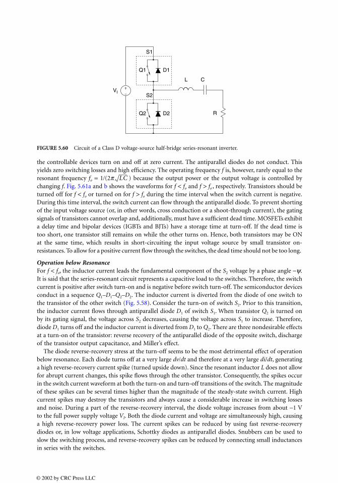
the controllable devices turn on and off at zero current. The antiparallel diodes do not conduct. Thisyields zero switching losses and high efficiency. The operating frequency f is, however, rarely equal to theresonant frequency fo = 1/(2π ) because the output power or the output voltage is controlled bychanging f. Fig. 5.61a and b shows the waveforms for f < fo and f > fo , respectively. Transistors should beturned off for f < fo or turned on for f > fo during the time interval when the switch current is negative.During this time interval, the switch current can flow through the antiparallel diode. To prevent shortingof the input voltage source (or, in other words, cross conduction or a shoot-through current), the gatingsignals of transistors cannot overlap and, additionally, must have a sufficient dead time. MOSFETs exhibita delay time and bipolar devices (IGBTs and BJTs) have a storage time at turn-off. If the dead time istoo short, one transistor still remains on while the other turns on. Hence, both transistors may be ONat the same time, which results in short-circuiting the input voltage source by small transistor on-resistances. To allow for a positive current flow through the switches, the dead time should not be too long.
Operation below ResonanceFor f < fo, the inductor current leads the fundamental component of the S2 voltage by a phase angle −ψ.It is said that the series-resonant circuit represents a capacitive load to the switches. Therefore, the switchcurrent is positive after switch turn-on and is negative before switch turn-off. The semiconductor devicesconduct in a sequence Q1–D1–Q2–D2. The inductor current is diverted from the diode of one switch tothe transistor of the other switch (Fig. 5.58). Consider the turn-on of switch S2. Prior to this transition,the inductor current flows through antiparallel diode D1 of switch S1. When transistor Q2 is turned onby its gating signal, the voltage across S2 decreases, causing the voltage across S1 to increase. Therefore,diode D1 turns off and the inductor current is diverted from D1 to Q2. There are three nondesirable effectsat a turn-on of the transistor: reverse recovery of the antiparallel diode of the opposite switch, dischargeof the transistor output capacitance, and Miller’s effect.
The diode reverse-recovery stress at the turn-off seems to be the most detrimental effect of operationbelow resonance. Each diode turns off at a very large dv/dt and therefore at a very large di/dt, generatinga high reverse-recovery current spike (turned upside down). Since the resonant inductor L does not allowfor abrupt current changes, this spike flows through the other transistor. Consequently, the spikes occurin the switch current waveform at both the turn-on and turn-off transitions of the switch. The magnitudeof these spikes can be several times higher than the magnitude of the steady-state switch current. Highcurrent spikes may destroy the transistors and always cause a considerable increase in switching lossesand noise. During a part of the reverse-recovery interval, the diode voltage increases from about −1 Vto the full power supply voltage VI. Both the diode current and voltage are simultaneously high, causinga high reverse-recovery power loss. The current spikes can be reduced by using fast reverse-recoverydiodes or, in low voltage applications, Schottky diodes as antiparallel diodes. Snubbers can be used toslow the switching process, and reverse-recovery spikes can be reduced by connecting small inductancesin series with the switches.
FIGURE 5.60 Circuit of a Class D voltage-source half-bridge series-resonant inverter.
R
L C
D2Q2
S2
Q1 D1
S1
VI
LC
© 2002 by CRC Press LLC
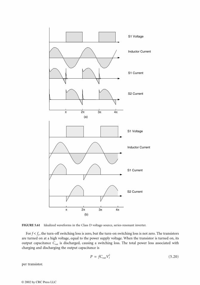
For f < fo , the turn-off switching loss is zero, but the turn-on switching loss is not zero. The transistorsare turned on at a high voltage, equal to the power supply voltage. When the transistor is turned on, itsoutput capacitance Cout is discharged, causing a switching loss. The total power loss associated withcharging and discharging the output capacitance is
(5.20)
per transistor.
FIGURE 5.61 Idealized waveforms in the Class D voltage-source, series-resonant inverter.
3π 4π
S1 Voltage
Inductor Current
S1 Current
S2 Current
(a)
2ππ
3π 4π(b)
2ππ
S1 Voltage
Inductor Current
S1 Current
S2 Current
P fCoutVI2=
© 2002 by CRC Press LLC
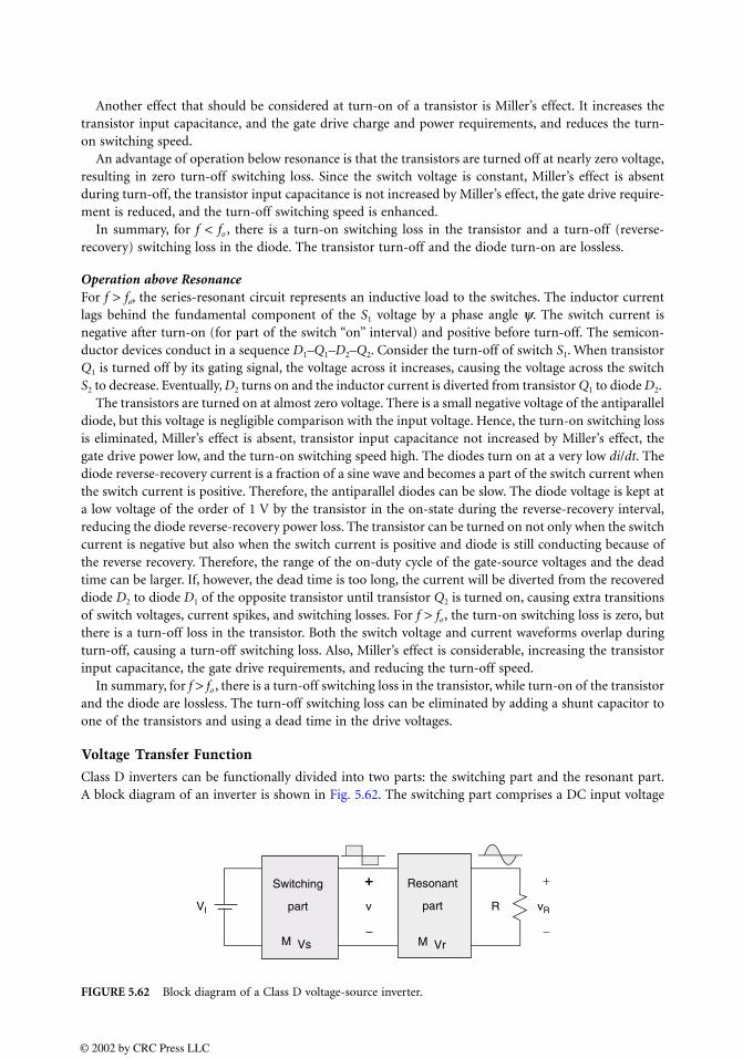
Another effect that should be considered at turn-on of a transistor is Miller’s effect. It increases thetransistor input capacitance, and the gate drive charge and power requirements, and reduces the turn-on switching speed.
An advantage of operation below resonance is that the transistors are turned off at nearly zero voltage,resulting in zero turn-off switching loss. Since the switch voltage is constant, Miller’s effect is absentduring turn-off, the transistor input capacitance is not increased by Miller’s effect, the gate drive require-ment is reduced, and the turn-off switching speed is enhanced.
In summary, for f < fo , there is a turn-on switching loss in the transistor and a turn-off (reverse-recovery) switching loss in the diode. The transistor turn-off and the diode turn-on are lossless.
Operation above ResonanceFor f > fo, the series-resonant circuit represents an inductive load to the switches. The inductor currentlags behind the fundamental component of the S1 voltage by a phase angle ψ. The switch current isnegative after turn-on (for part of the switch “on” interval) and positive before turn-off. The semicon-ductor devices conduct in a sequence D1–Q1–D2–Q2. Consider the turn-off of switch S1. When transistorQ1 is turned off by its gating signal, the voltage across it increases, causing the voltage across the switchS2 to decrease. Eventually, D2 turns on and the inductor current is diverted from transistor Q1 to diode D2.
The transistors are turned on at almost zero voltage. There is a small negative voltage of the antiparalleldiode, but this voltage is negligible comparison with the input voltage. Hence, the turn-on switching lossis eliminated, Miller’s effect is absent, transistor input capacitance not increased by Miller’s effect, thegate drive power low, and the turn-on switching speed high. The diodes turn on at a very low di/dt. Thediode reverse-recovery current is a fraction of a sine wave and becomes a part of the switch current whenthe switch current is positive. Therefore, the antiparallel diodes can be slow. The diode voltage is kept ata low voltage of the order of 1 V by the transistor in the on-state during the reverse-recovery interval,reducing the diode reverse-recovery power loss. The transistor can be turned on not only when the switchcurrent is negative but also when the switch current is positive and diode is still conducting because ofthe reverse recovery. Therefore, the range of the on-duty cycle of the gate-source voltages and the deadtime can be larger. If, however, the dead time is too long, the current will be diverted from the recovereddiode D2 to diode D1 of the opposite transistor until transistor Q2 is turned on, causing extra transitionsof switch voltages, current spikes, and switching losses. For f > fo, the turn-on switching loss is zero, butthere is a turn-off loss in the transistor. Both the switch voltage and current waveforms overlap duringturn-off, causing a turn-off switching loss. Also, Miller’s effect is considerable, increasing the transistorinput capacitance, the gate drive requirements, and reducing the turn-off speed.
In summary, for f > fo , there is a turn-off switching loss in the transistor, while turn-on of the transistorand the diode are lossless. The turn-off switching loss can be eliminated by adding a shunt capacitor toone of the transistors and using a dead time in the drive voltages.
Voltage Transfer Function
Class D inverters can be functionally divided into two parts: the switching part and the resonant part.A block diagram of an inverter is shown in Fig. 5.62. The switching part comprises a DC input voltage
FIGURE 5.62 Block diagram of a Class D voltage-source inverter.
© 2002 by CRC Press LLC

source VI and a set of switches. The switches are controlled to produce a square-wave voltage v. Since aresonant circuit forces a sinusoidal current, only the power of the fundamental component is transferredfrom the switching part to the resonant part. Hence, consideration of only the fundamental componentof the voltage at the input to the resonant circuit yields proper power relationships. A voltage transferfunction of the switching part can be defined as
(5.21)
where Vrms is the rms value of the fundamental component of the voltage v. For a half-bridge inverter, = /π = 0.45. In a full-bridge configuration, = 0.9. The resonant part of an inverter converts
a square-wave voltage v into sinusoidal current or voltage signal. The analysis of the Class D inverter of Fig. 5.60 is performed under an assumption that the semicon-
ductor devices and reactive components are ideal. Effects of nonidealities on inverter operation can befound in the literature, e.g., Ref. 3.
The parameters of the series-resonant circuit are defined as:
• The resonant frequency
(5.22)
• The characteristic impedance
(5.23)
and
• The loaded quality factor
(5.24)
The input impedance of the series-resonant circuit is
(5.25)
where
(5.26)
For f < fo , ψ is less than zero, which means that the resonant circuit represents a capacitive load to theswitching part of the inverter. For f > fo , ψ is greater than zero, which indicates that the resonant circuitrepresents an inductive load.
MVs
Vrms
VI
---------≡
MVs2 MVs
wo1
LC-----------=
ZoLC--- woL
1woC----------= = =
QwoL
R--------- 1
woCR--------------
Zo
R-----
LC---
R--------= = = =
Z Ze jyR j ωL1
ωC--------–
+ R 1 jQw
wo
------wo
w------–
+= =
y tan 1– Qw
wo
------wo
w------–
=
© 2002 by CRC Press LLC
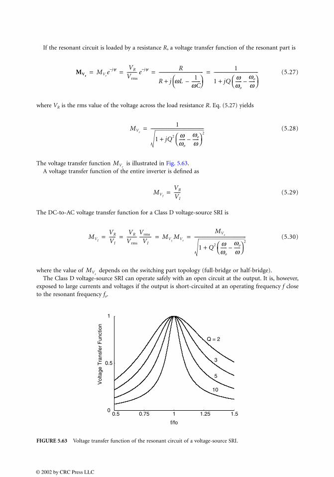
If the resonant circuit is loaded by a resistance R, a voltage transfer function of the resonant part is
(5.27)
where VR is the rms value of the voltage across the load resistance R. Eq. (5.27) yields
(5.28)
The voltage transfer function is illustrated in Fig. 5.63. A voltage transfer function of the entire inverter is defined as
(5.29)
The DC-to-AC voltage transfer function for a Class D voltage-source SRI is
(5.30)
where the value of depends on the switching part topology (full-bridge or half-bridge). The Class D voltage-source SRI can operate safely with an open circuit at the output. It is, however,
exposed to large currents and voltages if the output is short-circuited at an operating frequency f closeto the resonant frequency fo.
FIGURE 5.63 Voltage transfer function of the resonant circuit of a voltage-source SRI.
MVrMVr
e jψ– VR
Vrms
--------- e jψ– R
R j wL1
wC--------–
+---------------------------------------- 1
1 jQw
wo
------wo
w------–
+----------------------------------------= = = =
MVr
1
1 jQ2 wwo
------wo
w------–
2
+
------------------------------------------------=
MVr
MVI
VR
VI
------=
MVI
VR
VI
------VR
Vrms
---------Vrms
VI
----------- MVsMVr
MVs
1 Q2 wwo
------wo
w------–
2
+
-----------------------------------------------= = = =
MVs
0.5 0.75 1 1.25 1.50
0.5
1
f/fo
Vol
tage
Tra
nsfe
r F
unct
ion
Q = 2
3
5
10
© 2002 by CRC Press LLC
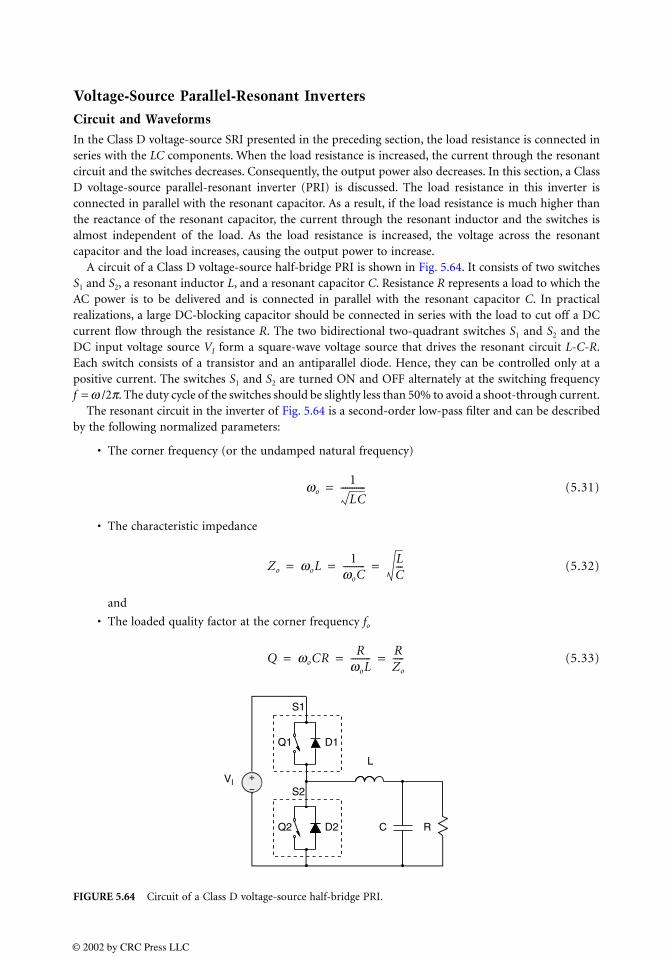
Voltage-Source Parallel-Resonant Inverters
Circuit and Waveforms
In the Class D voltage-source SRI presented in the preceding section, the load resistance is connected inseries with the LC components. When the load resistance is increased, the current through the resonantcircuit and the switches decreases. Consequently, the output power also decreases. In this section, a ClassD voltage-source parallel-resonant inverter (PRI) is discussed. The load resistance in this inverter isconnected in parallel with the resonant capacitor. As a result, if the load resistance is much higher thanthe reactance of the resonant capacitor, the current through the resonant inductor and the switches isalmost independent of the load. As the load resistance is increased, the voltage across the resonantcapacitor and the load increases, causing the output power to increase.
A circuit of a Class D voltage-source half-bridge PRI is shown in Fig. 5.64. It consists of two switchesS1 and S2, a resonant inductor L, and a resonant capacitor C. Resistance R represents a load to which theAC power is to be delivered and is connected in parallel with the resonant capacitor C. In practicalrealizations, a large DC-blocking capacitor should be connected in series with the load to cut off a DCcurrent flow through the resistance R. The two bidirectional two-quadrant switches S1 and S2 and theDC input voltage source VI form a square-wave voltage source that drives the resonant circuit L-C-R.Each switch consists of a transistor and an antiparallel diode. Hence, they can be controlled only at apositive current. The switches S1 and S2 are turned ON and OFF alternately at the switching frequencyf = ω /2π. The duty cycle of the switches should be slightly less than 50% to avoid a shoot-through current.
The resonant circuit in the inverter of Fig. 5.64 is a second-order low-pass filter and can be describedby the following normalized parameters:
• The corner frequency (or the undamped natural frequency)
(5.31)
• The characteristic impedance
(5.32)
and
• The loaded quality factor at the corner frequency fo
(5.33)
FIGURE 5.64 Circuit of a Class D voltage-source half-bridge PRI.
ωo1
LC-----------=
Zo ωoL1
ωoC---------- L
C---= = =
Q ωoCRR
ωoL--------- R
Zo
-----= = =
C R
L
D2Q2
S2
Q1 D1
S1
VI
© 2002 by CRC Press LLC
Using Eqs. (5.31) and (5.32), the input impedance of the resonant circuit can be expressed as
(5.34)
where
(5.35)
At f = fo,
(5.36)
As R is increased, Z( fo) decreases. The resonant frequency fr is defined as a frequency at which the phase shift ψ is zero. Hence, from
Eq. (5.35), the ratio of the resonant frequency fr to the corner frequency fo is
(5.37)
Frequency fr forms the boundary between inductive and capacitive loads. The following conclusions canbe drawn from Eq. (5.37):
1. For Q ≤ 1, the resonant frequency fr does not exist and the resonant circuit represents an inductiveload at any operating frequency.
2. For Q > 1, fr/fo increases with Q.
Current and voltage waveforms for f > fr are similar to those of Fig. 5.61b. The input voltage of the resonantcircuit is a square wave with a low-level value equal to zero (or to −VI in the full-bridge configuration)and a high-level value equal to VI. The analysis is simplified by assuming sinusoidal currents in L, C, andR. This approximation is valid if the loaded quality factor Q of the resonant circuit is high (e.g., Q ≥2.5). If Q < 2.5, the inductor current waveform differs from a sine wave and an accurate analytical solutionis more difficult to obtain. However, the predicted results are still qualitatively correct. A sinusoidalinductor current is assumed in the subsequent analysis. The inductor current i is conducted alternatelyby switches S1 and S2. Each transistor should be turned on when the switch current is negative and flowsthrough the diode. To achieve high efficiency and reliability, the switching frequency f should be higherthan fr under all operating conditions.
For f > fr , the phase shift ψ > 0, the resonant circuit represents an inductive load and the currenti lags behind the fundamental component of voltage v. Hence, the switch current is negative after turn-on and positive before turn-off. Consider the turn-off of switch S1. When transistor Q1 is turned off, itsvoltage increases, causing the decrease of the voltage of the other switch. As S2 voltage reaches −0.7 V, D2
turns on and therefore the current i is diverted from transistor Q1 to diode D2. The turn-off switchtransition is forced by the driver, while the turn-on transition of the switch is caused by the turn-offtransition of the opposite transistor, not by the driver. Only the turn-off transition is directly controllableby the driver. The transistor should be turned on by the driver when the switch current is negative and
Z Ze jy jωL
R1
jω C----------
R1
jωC----------+
--------------------+R 1
ωωo
------ 2
– j1Q---- ω
ωo
------ +
1 jQωωo
------ +
---------------------------------------------------------= = =
y tan 1– Qωωo
------ ω
ωo
------ 2 1
Q2------ 1–+
=
Z fo( )Zo
Q2 1+-------------------
Zo2
R----- for Q2 >> 1≈=
fr
fo
--- 11
Q2------– for Q 1≥=
© 2002 by CRC Press LLC
flows through the antiparallel diode. Therefore, the transistor is turned on at nearly zero voltage, reducingthe turn-on switching loss to a negligible level.
For f < fr, the phase shift ψ < 0, the resonant circuit represents a capacitive load for the switching part,and the inductor current i leads the fundamental component of the voltage v. Therefore, the antiparalleldiodes turn off at high di/dt, causing high current spikes in the switches and reducing efficiency andreliability. This problem can be alleviated by adding external diodes; however, the efficiency will bereduced.
Voltage Transfer Function
The voltage transfer function of the resonant circuit of Fig. 5.64 is
(5.38)
where
(5.39)
(5.40)
VR is the phasor of the voltage across R, and VR is the rms value of VR. Figure 5.65 shows the voltagetransfer function of the resonant circuit given by Eq. (5.39). From Eq. (5.39), = Q at f/fo = 1 and
(5.41)
With an open circuit at the output, increases from 1 to ∞ as ω/ωo is increased from zero to 1, and decreases from ∞ to zero as ω/ωo increases from 1 to ∞.
The maximum value of is obtained by differentiating the quantity under the square-root signwith respect to f/fo and setting the result equal to zero. Notice, however, that the maximum value of occurs at the frequency equal to zero for Q < . Hence, the normalized peak frequency is
(5.42)
MVr
VR
2Vrms
-----------------≡
RjωC----------
R1
jωC----------+
--------------------
jωL
RjωC----------
R1
jωC----------+
--------------------+
------------------------------------ 1
1ωωo
------ 2
– j1Q---- ω
ωo
------ +
------------------------------------------------ MVre jj= = =
MVr
VR
Vrms
--------- 1
1ωωo
------ 2
–2 1
Q2------ ω
ωo
------ 2
+--------------------------------------------------------------= =
j tan 1–
1Q---- ω
ωo
------
1ωωo
------ 2
–----------------------–=
MVr
MVr
1
1ωωo
------ 2
–---------------------- as Q ∞→→
MVr
MVr
MVr
MVr
1/ 2
fpk
fo
-----
0, for 0 Q1
2-------≤ ≤
11
2Q2---------– for Q
1
2------->
=
© 2002 by CRC Press LLC
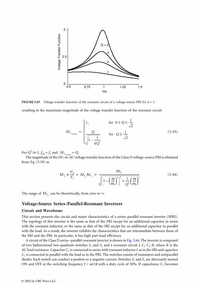
resulting in the maximum magnitude of the voltage transfer function of the resonant circuit
(5.43)
For , and .The magnitude of the DC-to-AC voltage transfer function of the Class D voltage-source PRI is obtained
from Eq. (5.39) as
(5.44)
The range of can be theoretically, from zero to ∞.
Voltage-Source Series–Parallel-Resonant Inverters
Circuit and Waveforms
This section presents the circuit and major characteristics of a series–parallel-resonant inverter (SPRI).The topology of this inverter is the same as that of the PRI except for an additional capacitor in serieswith the resonant inductor, or the same as that of the SRI except for an additional capacitor in parallelwith the load. As a result, the inverter exhibits the characteristics that are intermediate between those ofthe SRI and the PRI. In particular, it has high part-load efficiency.
A circuit of the Class D series –parallel-resonant inverter is shown in Fig. 5.66. The inverter is composedof two bidirectional two-quadrant switches S1 and S2 and a resonant circuit L-C1-C2-R, where R is theAC load resistance. Capacitor C1 is connected in series with resonant inductor L as in the SRI and capacitorC2 is connected in parallel with the load as in the PRI. The switches consist of transistors and antiparalleldiodes. Each switch can conduct a positive or a negative current. Switches S1 and S2 are alternately turnedON and OFF at the switching frequency f = ω/2π with a duty cycle of 50%. If capacitance C1 becomes
FIGURE 5.65 Voltage transfer function of the resonant circuit of a voltage-source PRI for A = 1.
0.5 0.75 1 1.25 1.50
2.5
5
f/fo
Vol
tage
Tra
nsfe
r F
unct
ion
Q = 5
3
2
1
MVr max( )
1, for 0 Q1
2-------≤ ≤
Q
11
4Q2---------–
---------------------- for Q1
2-------≥
=
Q2 >> 1 fpk fo≈ MVr max( )Q≈
MVI
VR
VI
------≡ MVsMVr
MVs
1ωωo
------ 2
–2 1
Q2------ ω
ωo
------ 2
+--------------------------------------------------------------= =
MVI
© 2002 by CRC Press LLC
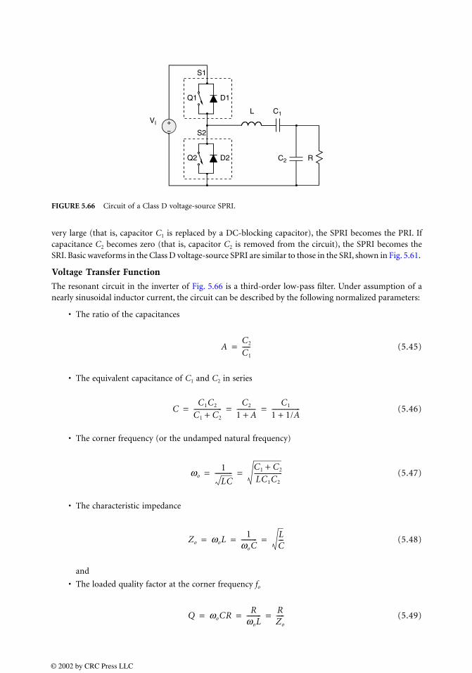
very large (that is, capacitor C1 is replaced by a DC-blocking capacitor), the SPRI becomes the PRI. Ifcapacitance C2 becomes zero (that is, capacitor C2 is removed from the circuit), the SPRI becomes theSRI. Basic waveforms in the Class D voltage-source SPRI are similar to those in the SRI, shown in Fig. 5.61.
Voltage Transfer Function
The resonant circuit in the inverter of Fig. 5.66 is a third-order low-pass filter. Under assumption of anearly sinusoidal inductor current, the circuit can be described by the following normalized parameters:
• The ratio of the capacitances
(5.45)
• The equivalent capacitance of C1 and C2 in series
(5.46)
• The corner frequency (or the undamped natural frequency)
(5.47)
• The characteristic impedance
(5.48)
and
• The loaded quality factor at the corner frequency fo
(5.49)
FIGURE 5.66 Circuit of a Class D voltage-source SPRI.
L
D2Q2
S2
Q1 D1
S1
VI
C1
RC2
AC2
C1
-----=
CC1C2
C1 C2+------------------
C2
1 A+------------
C1
1 1/A+------------------= = =
ωo1
LC-----------
C1 C2+LC1C2
------------------= =
Zo ωoL1
ωoC---------- L
C---= = =
Q ωoCRR
ωoL--------- R
Zo
-----= = =
© 2002 by CRC Press LLC
The input impedance of the resonant circuit shown in Fig. 5.64 is
(5.50)
where
(5.51)
and
(5.52)
At f/fo = 1,
(5.53)
and
(5.54)
Thus, Z decreases with increasing A and R at f = fo. Since ψ > 0, the resonant circuit always representsan inductive load for the switches at f = fo.
The resonant frequency fr is defined as the frequency at which the phase shift ψ is equal to zero. Thisfrequency forms the boundary between capacitive and inductive loads. For f < fr, ψ is less than zero andthe resonant circuit represents a capacitive load. Operation in this frequency range is not recommendedbecause the antiparallel diodes of the switches turn off at high di/dt, generating high reverse-recoverycurrent spikes. For f > fr, ψ > 0 and the resonant circuit represents an inductive load. Consequently, theinductor current i lags behind the fundamental component of the voltage vDS2. The antiparallel diodesturn off at low di/dt and do not generate reverse-recovery current spikes. Operation in this frequencyrange is recommended for practical applications. Setting ψ given in Eq. (5.52) to zero yields
(5.55)
The resonant frequency fr depends on Q and A. As Q → 0, fr /fo → 1/ .
Z Ze jy
R 1 A+( ) 1ωωo
------ 2
– j1Q---- ω
ωo
------ωo
ω------ A
A 1+------------–
+
1 jQωωo
------ 1 A+( )+
--------------------------------------------------------------------------------------------------------------= =
Z ZoQ
1 A+( )2 1ωωo
------ 2
–2 1
Q2------ ω
ωo
------ωo
ω------ A
A 1+------------–
2
+
1 Qωωo
------ 1 A+( )
2
+---------------------------------------------------------------------------------------------------------=
y tan 1– 1Q---- ω
ωo
------ωo
ω------ A
A 1+------------–
Q 1 A+( )2 ωωo
------ 1
ωωo
------ 2
––
=
ZZo
1 A+( ) 1 Q2 1 A+( )2+----------------------------------------------------------
Zo2
R 1 A+( )2----------------------- for Q2 1 A+( )2 >> 1≈=
y tan 1– 1Q 1 A+( )----------------------=
fr
fo
--- Q2 1 A+( )2 1– Q2 1 A+( )2 1–[ ]24Q2A 1 A+( )++
2Q2 1 A+( )2------------------------------------------------------------------------------------------------------------------------------=
1 1/A+
© 2002 by CRC Press LLC
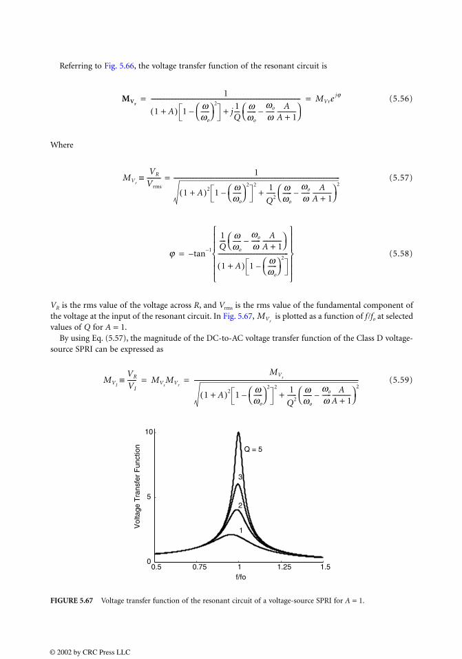
Referring to Fig. 5.66, the voltage transfer function of the resonant circuit is
(5.56)
Where
(5.57)
(5.58)
VR is the rms value of the voltage across R, and Vrms is the rms value of the fundamental component ofthe voltage at the input of the resonant circuit. In Fig. 5.67, is plotted as a function of f/fo at selectedvalues of Q for A = 1.
By using Eq. (5.57), the magnitude of the DC-to-AC voltage transfer function of the Class D voltage-source SPRI can be expressed as
(5.59)
FIGURE 5.67 Voltage transfer function of the resonant circuit of a voltage-source SPRI for A = 1.
MVr
1
1 A+( ) 1ωωo
------ 2
– j1Q---- ω
ωo
------ωo
ω------ A
A 1+------------–
+-------------------------------------------------------------------------------------------------- MVre
jj= =
MVr
VR
Vrms
--------- 1
1 A+( )2 1ωωo
------ 2
–2 1
Q2------ ω
ωo
------ωo
ω------ A
A 1+------------–
2
+
-------------------------------------------------------------------------------------------------------------=≡
ϕ tan 1–
1Q---- ω
ωo
------ωo
ω------ A
A 1+------------–
1 A+( ) 1ωωo
------ 2
–----------------------------------------------
–=
MVr
MVI
VR
VI
------≡ MVsMVr
MVs
1 A+( )2 1ωωo
------ 2
–2 1
Q2------ ω
ωo
------ωo
ω------ A
A 1+------------–
2
+
------------------------------------------------------------------------------------------------------------= =
0.5 0.75 1 1.25 1.50
5
10
f/fo
Vol
tage
Tra
nsfe
r F
unct
ion Q = 5
3
2
1
© 2002 by CRC Press LLC
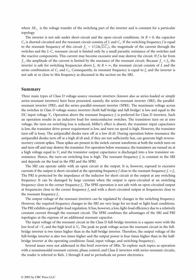
where is the voltage transfer of the switching part of the inverter and is constant for a particulartopology.
The inverter is not safe under short-circuit and the open-circuit conditions. At R = 0, the capacitorC2 is shorted-circuited and the resonant circuit consists of L and C1. If the switching frequency f is equalto the resonant frequency of this circuit = 1/(2π ), the magnitude of the current through theswitches and the L-C1 resonant circuit is limited only by a small parasitic resistance of the switches andthe reactive components. This current may become excessive and may destroy the circuit. If f is far from
, the amplitude of the current is limited by the reactance of the resonant circuit. Because < fo, theinverter is safe for switching frequencies above fo. At R = ∞, the resonant circuit consists of L and theseries combination of C1 and C2. Consequently, its resonant frequency is equal to fo and the inverter isnot safe at or close to this frequency as discussed in the section on the SRI.
Summary
Three main types of Class D voltage-source resonant inverters (known also as series-loaded or simplyseries-resonant inverters) have been presented, namely, the series-resonant inverter (SRI), the parallel-resonant inverter (PRI), and the series–parallel-resonant inverter (SPRI). The maximum voltage acrossthe switches in Class D voltage-source inverters (both half-bridge and full-bridge) is low and equal to theDC input voltage VI. Operation above the resonant frequency fr is preferred for Class D inverters. Suchan operation results in an inductive load for semiconductor switches. The transistors turn on at zerovoltage, the turn-on switching loss is reduced, Miller’s effect is absent, the transistor input capacitanceis low, the transistor drive-power requirement is low, and turn-on speed is high. However, the transistorturn-off is lossy. The antiparallel diodes turn off at a low di/dt. During operation below resonance theantiparallel diodes turn off at a high di/dt and, if they are not sufficiently fast, can generate high reverse-recovery current spikes. These spikes are present in the switch current waveforms at both the switch turn-onand turn-off and may destroy the transistor. For operation below resonance, the transistors are turned on ata high voltage equal to VI and the transistor output capacitance is discharged into a low transistor on-resistance. Hence, the turn-on switching loss is high. The resonant frequency fr is constant in the SRIand depends on the load in the PRI and the SPRI.
The SRI can operate safely with an open circuit at the output. It is, however, exposed to excessivecurrents if the output is short-circuited at the operating frequency f close to the resonant frequency fr = fo.The PRI is protected by the impedance of the inductor for short circuit at the output at any switchingfrequency. It can be damaged by large currents when the output is open-circuited at an switchingfrequency close to the corner frequency fo. The SPRI operation is not safe with an open-circuited outputat frequencies close to the corner frequency fo and with a short-circuited output at frequencies close tothe resonant frequency fr .
The output voltage of the resonant inverters can be regulated by changes in the switching frequency.However, the required frequency changes in the SRI are very large for no-load or light-load conditions.The PRI exhibits a good light-load regulation. It has, however, a low, light-load efficiency due to a relativelyconstant current through the resonant circuit. The SPRI combines the advantages of the SRI and PRItopologies at the expense of an additional resonant capacitor.
The input voltage of the resonant circuit in the Class D full-bridge inverters is a square wave with thelow level of −VI and the high level is VI. The peak-to-peak voltage across the resonant circuit in the full-bridge inverter is two times higher than in the half-bridge inverter. Therefore, the output voltage of thefull-bridge inverter is also two times higher and the output power is four times higher than in the half-bridge inverter at the operating conditions (load, input voltage, and switching frequency).
Several issues were not addressed in this brief overview of SRIs. To explore such topics as operationwith a nonsinusoidal resonant current, phase control, and Class E inverters with series-resonant circuits,the reader is referred to Refs. 2 through 8 and to periodicals on power electronics.
MVs
frsLC1
frsfrs
© 2002 by CRC Press LLC
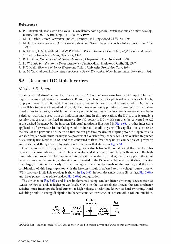
References
1. P. J. Baxandall, Transistor sine-wave LC oscillators, some general considerations and new develop-ments, Proc. IEE 13, 106(suppl. 16), 748–758, 1959.
2. M. H. Rashid, Power Electronics, 2nd ed., Prentice-Hall, Englewood Cliffs, NJ, 1993. 3. M. K. Kazimierczuk and D. Czarkowski, Resonant Power Converters, Wiley Interscience, New York,
1995. 4. N. Mohan, T. M. Undeland, and W. P. Robbins, Power Electronics: Converters, Applications and Design,
2nd ed., John Wiley & Sons, New York, 1995. 5. R. Erickson, Fundamentals of Power Electronics, Chapman & Hall, New York, 1997. 6. D. W. Hart, Introduction to Power Electronics, Prentice-Hall, Englewood Cliffs, NJ, 1997. 7. P. T. Krein, Elements of Power Electronics, Oxford University Press, New York, 1998. 8. A. M. Trzynadlowski, Introduction to Modern Power Electronics, Wiley Interscience, New York, 1998.
5.5 Resonant DC-Link Inverters
Michael E. Ropp
Inverters are DC-to-AC converters; they create an AC output waveform from a DC input. They arerequired in any application that involves a DC source, such as batteries, photovoltaic arrays, or fuel cells,supplying power to an AC load. Inverters are also frequently used in applications in which AC with acontrollable frequency is required. Probably the most common application of inverters is in variable-speed drives for motors, in which the frequency of the AC output of the inverters is controlled to obtaina desired rotational speed from an induction machine. In this application, the DC source is usually arectifier that converts the fixed-frequency utility AC power to DC, which can then be converted to ACat the desired frequency by the inverter. This configuration is illustrated in Fig. 5.68. Another interestingapplication of inverters is in interfacing wind turbines to the utility system. This application is in a sensethe dual of the previous one; the wind turbine can produce maximum output power if it operates at avariable frequency, but then its output AC power is at a variable frequency as well. This variable-frequencyAC is usually first rectified to DC and then converted to fixed-frequency utility-compatible AC power byan inverter, and the system configuration is the same as that shown in Fig. 5.68.
One feature of this configuration is the large capacitor between the rectifier and the inverter. Thiscapacitor is commonly called the DC-link capacitor, and it is usually quite large with values in the highhundreds of microfarads. The purpose of this capacitor is to absorb, or filter, the large ripple in the inputcurrent drawn by the inverter, so that it is not presented to the DC source. Because the DC-link capacitoris so large, it maintains a nearly constant voltage at the input terminals of the inverter, and thus thecombination of this large capacitor with the inverter circuit is referred to as a voltage-source inverter(VSI) topology [1,2]. This topology is shown in Fig. 5.67, in both the single-phase (H-bridge, Fig. 5.69a)and three-phase (three-phase bridge, Fig. 5.69a) configurations.
The switches in Fig. 5.69a and b are implemented using semiconductor switching devices such asIGBTs, MOSFETs, and, at higher power levels, GTOs. In the VSI topologies shown, the semiconductorswitches must interrupt the load current at high voltage, a technique known as hard switching. Hardswitching results in energy dissipation in the semiconductor switches at each on–off or off–on transition.
FIGURE 5.68 Back-to-back AC-DC-AC converter used in motor drives and wind energy conversion systems.
© 2002 by CRC Press LLC
While a semiconductor switch is off, there is essentially zero current flowing through the switch, so thetotal power dissipation in the switch is nearly zero. When the switch is on, the current through the switchis large, but the voltage is small, so the amount of power dissipated in the switch is relatively low. However,during a transition from on to off, the current is decreasing from its “on”-state value while the voltageis increasing to its “off”-state value, and both are simultaneously high for a short period. During thisperiod, the power dissipation in the switch is high. A similar situation occurs during the off-to-ontransition. Such losses occurring during switch state transitions are commonly called switching losses,and they can make up as much as 50% of the total losses in the VSI [3]. Switching losses obviously reducethe efficiency of the converter. However, such losses also significantly impact the thermal design andpackaging of VSIs. The power lost in the switches is dissipated as heat, which must be removed from theswitch to avoid damage. Removing the heat requires large heat sinks, which increase converter size andcost, and possibly fans, which decrease reliability and efficiency.
As the switching frequency (the inverse of the period of the switching cycle) increases, the number ofswitching transitions per unit time also increases. More energy is dissipated in the switch during a shortertime, and therefore the power dissipation in the switches increases as the switching frequency increases.Thus, it might be thought that decreasing the switching frequency would ease the switching loss problem.Unfortunately, it is desirable to significantly increase the switching frequency for many reasons. Primaryamong these is that the energy storage elements (inductors and capacitors) can be made smaller if theswitching frequency is higher [4], allowing for increased power density and lower cost. Higher switchingfrequencies also improve power quality in pulse width–modulated (PWM) inverters because the har-monics produced are concentrated at multiples of the switching frequency and closely spaced sidebands[5]. High switching frequencies also enable the inverter to respond more rapidly to control signals,increasing the “control bandwidth” of the converter. The factor in most VSIs that prevents switchingfrequencies from being increased to realize these benefits is the switching loss and subsequent thermalmanagement of the semiconductor switches (hard-switched VSIs are often said to be “thermally limited”for this reason).
It is evident that reducing or eliminating switching loss would be highly beneficial to VSI design, notonly for efficiency and thermal management reasons, but also because it would improve reliability,
FIGURE 5.69 (a) Single-phase DC-AC inverter (H-bridge); (b) three-phase DC-AC inverter (three-phase bridge).
© 2002 by CRC Press LLC
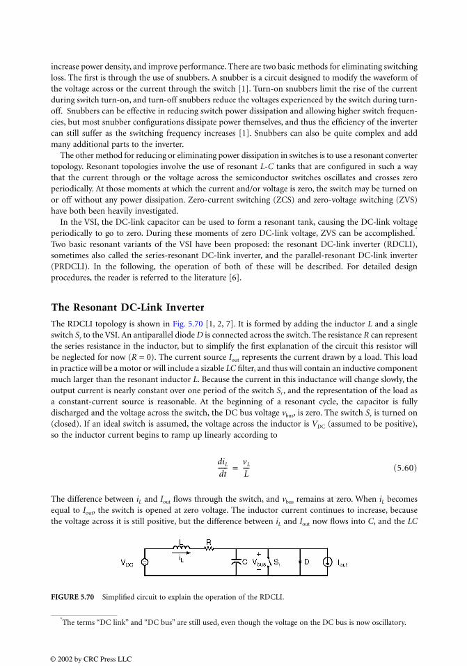
increase power density, and improve performance. There are two basic methods for eliminating switchingloss. The first is through the use of snubbers. A snubber is a circuit designed to modify the waveform ofthe voltage across or the current through the switch [1]. Turn-on snubbers limit the rise of the currentduring switch turn-on, and turn-off snubbers reduce the voltages experienced by the switch during turn-off. Snubbers can be effective in reducing switch power dissipation and allowing higher switch frequen-cies, but most snubber configurations dissipate power themselves, and thus the efficiency of the invertercan still suffer as the switching frequency increases [1]. Snubbers can also be quite complex and addmany additional parts to the inverter.
The other method for reducing or eliminating power dissipation in switches is to use a resonant convertertopology. Resonant topologies involve the use of resonant L-C tanks that are configured in such a waythat the current through or the voltage across the semiconductor switches oscillates and crosses zeroperiodically. At those moments at which the current and/or voltage is zero, the switch may be turned onor off without any power dissipation. Zero-current switching (ZCS) and zero-voltage switching (ZVS)have both been heavily investigated.
In the VSI, the DC-link capacitor can be used to form a resonant tank, causing the DC-link voltageperiodically to go to zero. During these moments of zero DC-link voltage, ZVS can be accomplished.
*
Two basic resonant variants of the VSI have been proposed: the resonant DC-link inverter (RDCLI),sometimes also called the series-resonant DC-link inverter, and the parallel-resonant DC-link inverter(PRDCLI). In the following, the operation of both of these will be described. For detailed designprocedures, the reader is referred to the literature [6].
The Resonant DC-Link Inverter
The RDCLI topology is shown in Fig. 5.70 [1, 2, 7]. It is formed by adding the inductor L and a singleswitch Sr to the VSI. An antiparallel diode D is connected across the switch. The resistance R can representthe series resistance in the inductor, but to simplify the first explanation of the circuit this resistor willbe neglected for now (R = 0). The current source Iout represents the current drawn by a load. This loadin practice will be a motor or will include a sizable LC filter, and thus will contain an inductive componentmuch larger than the resonant inductor L. Because the current in this inductance will change slowly, theoutput current is nearly constant over one period of the switch Sr , and the representation of the load asa constant-current source is reasonable. At the beginning of a resonant cycle, the capacitor is fullydischarged and the voltage across the switch, the DC bus voltage vbus, is zero. The switch Sr is turned on(closed). If an ideal switch is assumed, the voltage across the inductor is VDC (assumed to be positive),so the inductor current begins to ramp up linearly according to
(5.60)
The difference between iL and Iout flows through the switch, and vbus remains at zero. When iL becomesequal to Iout, the switch is opened at zero voltage. The inductor current continues to increase, becausethe voltage across it is still positive, but the difference between iL and Iout now flows into C, and the LC
*The terms “DC link” and “DC bus” are still used, even though the voltage on the DC bus is now oscillatory.
FIGURE 5.70 Simplified circuit to explain the operation of the RDCLI.
diL
dt------
vL
L----=
© 2002 by CRC Press LLC
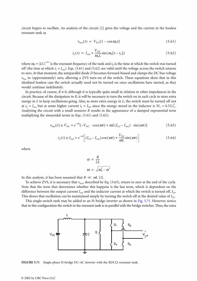
circuit begins to oscillate. An analysis of the circuit [2] gives the voltage and the current in the losslessresonant tank as
(5.61)
(5.62)
where ω0 = (LC)−0.5
is the resonant frequency of the tank and t0 is the time at which the switch was turnedoff (the time at which iL = Iout). Eqs. (5.61) and (5.62) are valid until the voltage across the switch returnsto zero. At that moment, the antiparallel diode D becomes forward-biased and clamps the DC bus voltagevbus to (approximately) zero, allowing a ZVS turn-on of the switch. These equations show that in thisidealized lossless case the switch actually need not be turned on once oscillations have started, as theywould continue indefinitely.
In practice, of course, R ≠ 0, although it is typically quite small in relation to other impedances in thecircuit. Because of the dissipation in R, it will be necessary to turn the switch on in each cycle to store extraenergy in L to keep oscillations going. Also, to store extra energy in L, the switch must be turned off notat iL = Iout but at some higher current iL = IL0, since the energy stored in the inductor is WL = 0.5 .Analyzing the circuit with a small nonzero R results in the appearance of a damped exponential termmultiplying the sinusoidal terms in Eqs. (5.61) and (5.62):
(5.63)
(5.64)
where
In this analysis, it has been assumed that R ωL [2]. To achieve ZVS, it is necessary that vbus, described by Eq. (5.63), return to zero at the end of the cycle.
Note that the term that determines whether this happens is the last term, which is dependent on thedifference between the output current Iout and the inductor current at which the switch is turned off, IL0.This shows that oscillation can be maintained simply by turning the switch off at the desired value of IL0.
This single-switch tank may be added to an H-bridge inverter as shown in Fig. 5.71. However, noticethat in this configuration the switch in the resonant tank is in parallel with the bridge switches. Thus, the extra
FIGURE 5.71 Single-phase H-bridge DC-AC inverter with the RDCLI resonant tank.
vbus t( ) VDC 1 ω0tcos–[ ]=
iL t( ) Iout
VDC
ω0L---------- ω0 t t0–[ ]( )sin+=
LiL2
vbus t( ) VDC e at– VDC wt( ) wL IL0 Iout–( ) wt( )sin⋅+cos⋅–[ ]+≅
iL t( ) Iout e at– IL0 Iout–( ) wt( )VDC
wL--------- wt( )sin+cos+≅
α R2L------=
w w02 α 2–=
<<
© 2002 by CRC Press LLC
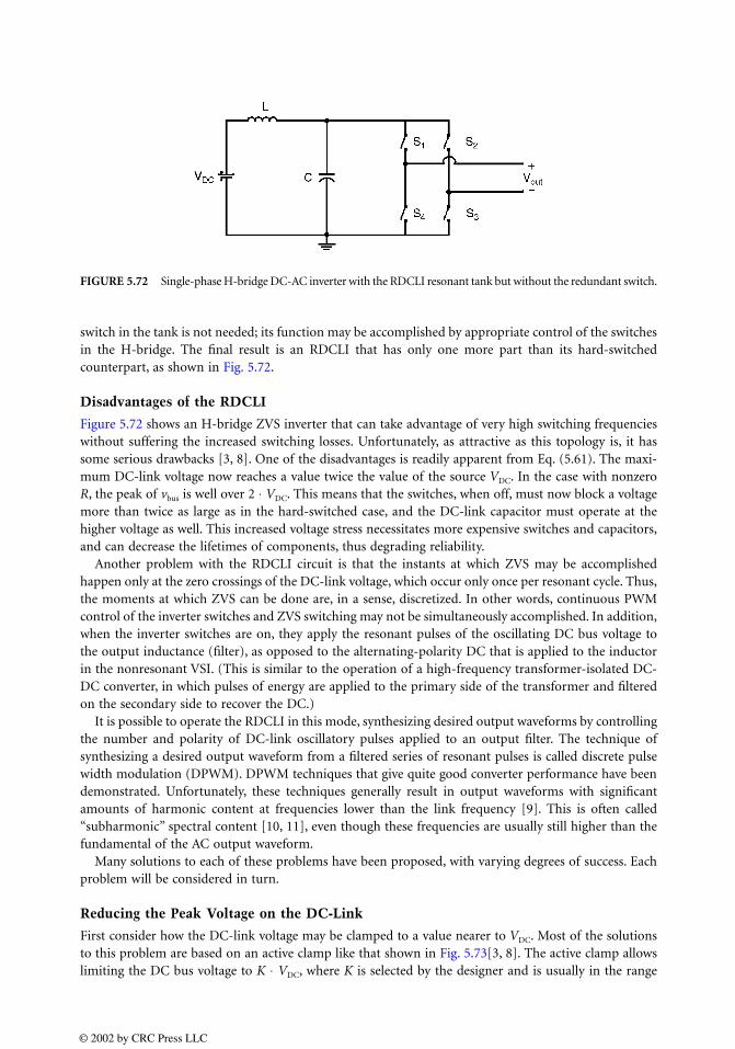
switch in the tank is not needed; its function may be accomplished by appropriate control of the switchesin the H-bridge. The final result is an RDCLI that has only one more part than its hard-switchedcounterpart, as shown in Fig. 5.72.
Disadvantages of the RDCLI
Figure 5.72 shows an H-bridge ZVS inverter that can take advantage of very high switching frequencieswithout suffering the increased switching losses. Unfortunately, as attractive as this topology is, it hassome serious drawbacks [3, 8]. One of the disadvantages is readily apparent from Eq. (5.61). The maxi-mum DC-link voltage now reaches a value twice the value of the source VDC. In the case with nonzeroR, the peak of vbus is well over 2 ⋅ VDC. This means that the switches, when off, must now block a voltagemore than twice as large as in the hard-switched case, and the DC-link capacitor must operate at thehigher voltage as well. This increased voltage stress necessitates more expensive switches and capacitors,and can decrease the lifetimes of components, thus degrading reliability.
Another problem with the RDCLI circuit is that the instants at which ZVS may be accomplishedhappen only at the zero crossings of the DC-link voltage, which occur only once per resonant cycle. Thus,the moments at which ZVS can be done are, in a sense, discretized. In other words, continuous PWMcontrol of the inverter switches and ZVS switching may not be simultaneously accomplished. In addition,when the inverter switches are on, they apply the resonant pulses of the oscillating DC bus voltage tothe output inductance (filter), as opposed to the alternating-polarity DC that is applied to the inductorin the nonresonant VSI. (This is similar to the operation of a high-frequency transformer-isolated DC-DC converter, in which pulses of energy are applied to the primary side of the transformer and filteredon the secondary side to recover the DC.)
It is possible to operate the RDCLI in this mode, synthesizing desired output waveforms by controllingthe number and polarity of DC-link oscillatory pulses applied to an output filter. The technique ofsynthesizing a desired output waveform from a filtered series of resonant pulses is called discrete pulsewidth modulation (DPWM). DPWM techniques that give quite good converter performance have beendemonstrated. Unfortunately, these techniques generally result in output waveforms with significantamounts of harmonic content at frequencies lower than the link frequency [9]. This is often called“subharmonic” spectral content [10, 11], even though these frequencies are usually still higher than thefundamental of the AC output waveform.
Many solutions to each of these problems have been proposed, with varying degrees of success. Eachproblem will be considered in turn.
Reducing the Peak Voltage on the DC-Link
First consider how the DC-link voltage may be clamped to a value nearer to VDC. Most of the solutionsto this problem are based on an active clamp like that shown in Fig. 5.73[3, 8]. The active clamp allowslimiting the DC bus voltage to K ⋅ VDC, where K is selected by the designer and is usually in the range
FIGURE 5.72 Single-phase H-bridge DC-AC inverter with the RDCLI resonant tank but without the redundant switch.
© 2002 by CRC Press LLC
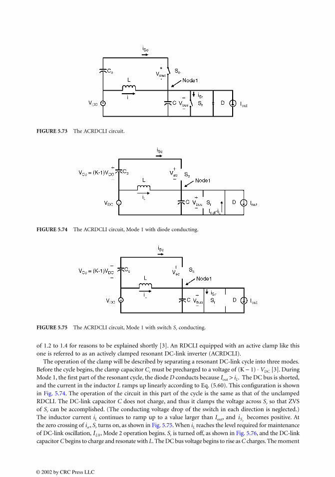
of 1.2 to 1.4 for reasons to be explained shortly [3]. An RDCLI equipped with an active clamp like thisone is referred to as an actively clamped resonant DC-link inverter (ACRDCLI).
The operation of the clamp will be described by separating a resonant DC-link cycle into three modes.Before the cycle begins, the clamp capacitor Cc must be precharged to a voltage of (K − 1) ⋅ VDC [3]. DuringMode 1, the first part of the resonant cycle, the diode D conducts because Iout > iL. The DC bus is shorted,and the current in the inductor L ramps up linearly according to Eq. (5.60). This configuration is shownin Fig. 5.74. The operation of the circuit in this part of the cycle is the same as that of the unclampedRDCLI. The DC-link capacitor C does not charge, and thus it clamps the voltage across Sr so that ZVSof Sr can be accomplished. (The conducting voltage drop of the switch in each direction is neglected.)The inductor current iL continues to ramp up to a value larger than Iout, and becomes positive. Atthe zero crossing of isr, Sr turns on, as shown in Fig. 5.75. When iL reaches the level required for maintenanceof DC-link oscillation, , Mode 2 operation begins. Sr is turned off, as shown in Fig. 5.76, and the DC-linkcapacitor C begins to charge and resonate with L. The DC bus voltage begins to rise as C charges. The moment
FIGURE 5.73 The ACRDCLI circuit.
FIGURE 5.74 The ACRDCLI circuit, Mode 1 with diode conducting.
FIGURE 5.75 The ACRDCLI circuit, Mode 1 with switch Sr conducting.
iSr
IL0
© 2002 by CRC Press LLC
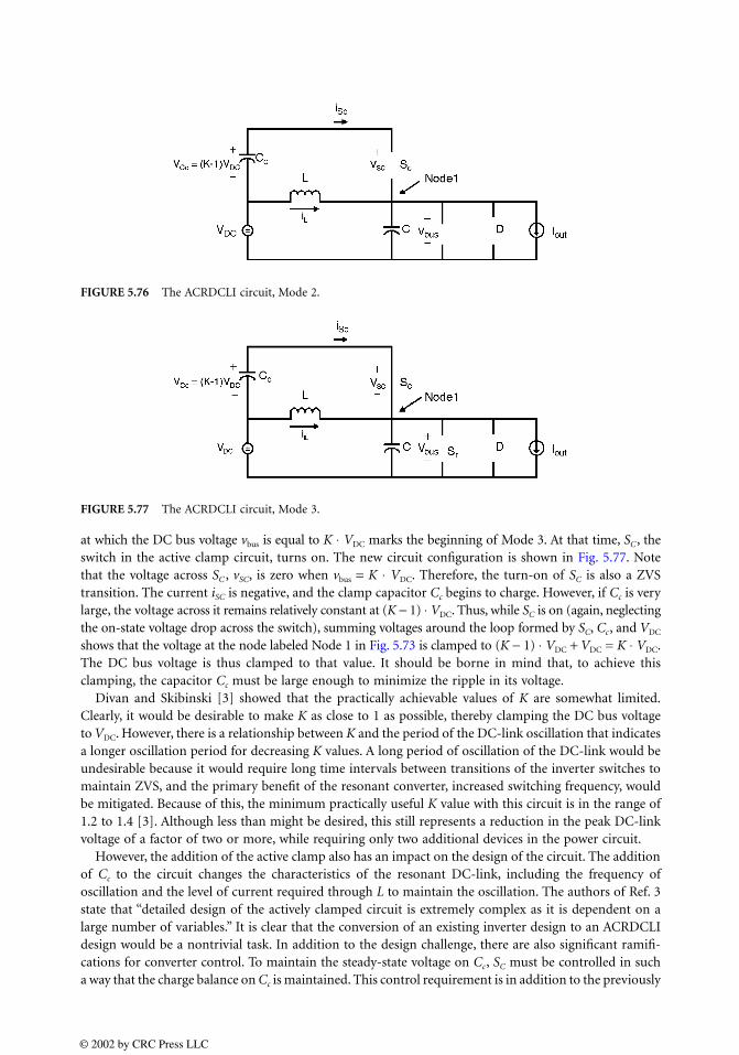
at which the DC bus voltage vbus is equal to K ⋅ VDC marks the beginning of Mode 3. At that time, SC, theswitch in the active clamp circuit, turns on. The new circuit configuration is shown in Fig. 5.77. Notethat the voltage across SC , vSC, is zero when vbus = K ⋅ VDC. Therefore, the turn-on of SC is also a ZVStransition. The current iSC is negative, and the clamp capacitor Cc begins to charge. However, if Cc is verylarge, the voltage across it remains relatively constant at (K − 1) ⋅ VDC. Thus, while SC is on (again, neglectingthe on-state voltage drop across the switch), summing voltages around the loop formed by SC, Cc, and VDC
shows that the voltage at the node labeled Node 1 in Fig. 5.73 is clamped to (K − 1) ⋅ VDC + VDC = K ⋅ VDC.The DC bus voltage is thus clamped to that value. It should be borne in mind that, to achieve thisclamping, the capacitor Cc must be large enough to minimize the ripple in its voltage.
Divan and Skibinski [3] showed that the practically achievable values of K are somewhat limited.Clearly, it would be desirable to make K as close to 1 as possible, thereby clamping the DC bus voltageto VDC. However, there is a relationship between K and the period of the DC-link oscillation that indicatesa longer oscillation period for decreasing K values. A long period of oscillation of the DC-link would beundesirable because it would require long time intervals between transitions of the inverter switches tomaintain ZVS, and the primary benefit of the resonant converter, increased switching frequency, wouldbe mitigated. Because of this, the minimum practically useful K value with this circuit is in the range of1.2 to 1.4 [3]. Although less than might be desired, this still represents a reduction in the peak DC-linkvoltage of a factor of two or more, while requiring only two additional devices in the power circuit.
However, the addition of the active clamp also has an impact on the design of the circuit. The additionof Cc to the circuit changes the characteristics of the resonant DC-link, including the frequency ofoscillation and the level of current required through L to maintain the oscillation. The authors of Ref. 3state that “detailed design of the actively clamped circuit is extremely complex as it is dependent on alarge number of variables.” It is clear that the conversion of an existing inverter design to an ACRDCLIdesign would be a nontrivial task. In addition to the design challenge, there are also significant ramifi-cations for converter control. To maintain the steady-state voltage on Cc, SC must be controlled in sucha way that the charge balance on Cc is maintained. This control requirement is in addition to the previously
FIGURE 5.76 The ACRDCLI circuit, Mode 2.
FIGURE 5.77 The ACRDCLI circuit, Mode 3.
© 2002 by CRC Press LLC

described requirements on Sr to maintain the oscillation of the DC-link. Suitable control methods aredescribed in the literature [3], but clearly the complexity of the controller will be increased somewhatby the addition of the active clamp. In summary, the ACRDCLI does reduce the problem of the high DCbus voltage found in the RDCLI, but its design and control are much more difficult.
A significant number of variants of this circuit have been described. Many ACRDCLI topologies havebeen recently devised with the objective of clamping the maximum DC-link voltage to VDC, thus realizinga K value of 1. Such a converter is typically termed a source-clamped RDCLI [12]. Other ACRDCLIvariants have been designed to eliminate the need for precharging the clamp capacitor [13,14]. As mightbe expected, most of these variants improve the converter performance at the expense of a more-complicated circuit, and more difficult design and control.
Achieving Continuous PWM Control with the RDCLI: The Quasi-RDCLI
As was previously described, the necessity of synchronizing the transitions of the inverter bridge switcheswith the zero-voltage periods of the oscillating DC-link voltage creates a conflict that leads to a loss ofoutput waveform quality and a narrowly limited range of controllability. Early attempts to solve thisproblem within the constraints of DPWM focused on the use of advanced control techniques [15, 16] toimprove the converter performance without modification of the circuit topology. Such control techniqueswere used with considerable success and were shown to be capable of partially eliminating the problemsof DPWM and giving RDCLI performance sufficient for many applications. Another technique intendedto give PWM control while only slightly modifying the circuit and not adding semiconductor switcheshas been described [10]. This method requires placing a snubber capacitor in parallel with each semi-conductor switch, and then using these snubber capacitors collectively to replace the DC-link capacitor.Unfortunately, this circuit had significantly higher losses than the original RDCLI [15], and the range ofPWM control possible was found to be rather limited.
To obtain true continuous PWM control, the ACRDCLI circuit must be modified in such a way thatthe zero crossings of the DC bus voltage are controllable. Clearly, such a circuit must interrupt or modifythe oscillation of the resonant tank, and for this reason circuits that implement this concept are calledquasi-resonant DC-link inverters (QRDCLIs). QRDCLIs use a network of semiconductor switches, induc-tors, capacitors, and sometimes transformers to shape and control the resonant cycle of the DC bus.Several QRDCLI topologies have been proposed [17–23], all of which also contain an active (or passive)clamp. However, no single superior QRDCLI topology has yet been demonstrated. Because of the myriadrequirements of achieving charge balance on all capacitors, volt-second balance on all inductors, andZVS or ZCS of all switches in the added circuit, all the QRDCLI devices proposed thus far involvesignificant numbers of components, complicated control, and difficult design. To summarize, then, theQRDCLI enables ZVS or ZCS operation of all the switches in the circuit, with lower voltage stresses thanthe RDCLI, and with true PWM capability. It does so at the expense of an increased parts count, a higherlevel of difficulty in design, and greater complexity of control.
The Parallel-Resonant DC-Link Inverter
Shortly after the initial proposal of the RDCLI, a different topology was proposed to allow ZVS operationof VSIs. This topology, shown in Fig. 5.78, is the parallel-resonant DC-link inverter (PRDCLI) [24]. Asbefore, the inverter current is represented as a constant current source.
Consider the operation of the PRDCLI [24]. The circuit has seven modes of operation. Initially, thecircuit is in Mode 1, switches Sr1 and Sr3 are both on, and Sr2 and Sr4 are both off, as shown in Fig. 5.79.The source supplies the inverter current through Sr1, and the two capacitors C1 and C2 appear in paralleland are both charged to the DC bus voltage vbus. Before an inverter switch transition is commanded, theparallel-resonant circuit drives the DC bus voltage to zero. This is accomplished as follows. The circuitenters Mode 2 when switch Sr2 is turned on, as shown in Fig. 5.80. This is a ZCS transition, becauseduring the switch transition the current iL cannot change instantaneously and is clamped to zero. Thevoltage across L is vbus because both Sr2 and Sr3 are on, so iL begins to ramp up according to Eq. (5.60).
© 2002 by CRC Press LLC
The inductor current ramps up until it reaches a critical value ILo. As was the case in the RDCLI, must be chosen such that there is sufficient energy stored in the inductor to allow vbus to go all the wayto zero during the resonant cycle to follow.
As soon as iL = ILo, Sr1 is turned off, and the circuit configuration becomes that shown in Fig. 5.81.This initiates Mode 3. C1 and C2 begin to discharge and resonate with L. Because the voltage across L,vbus, is still positive, iL continues to ramp up to a resonant peak current higher than ILo. When iL reachesits peak current, the DC bus voltage vbus will be zero. At that moment, Mode 4 begins. Switch Sr3 turnsoff and Sr4 turns on, as shown in Fig. 5.82. This effectively separates the PRDCLI into two subcircuits,the resonant circuit with C1 and L and the output circuit consisting of C2, Sr4, and the inverter. In thisconfiguration, since Sr4 shorts the DC bus, vbus is zero and is clamped to zero by C2. The inverter devicesmay now be switched under ZVS conditions. Capacitor C1 and inductor L continue to resonate, with vC1
and iL passing through negative peaks. When iL reaches its negative peak value, Mode 5 operation begins.In this mode, the energy stored in the inductor is used to recharge the two capacitors and reset the circuitto its initial condition so that the resonant cycle may begin again when needed. To do this, Sr3 turns onunder ZCS and Sr4 turns off under ZVS, returning the circuit to the configuration shown in Fig. 5.81and initiating Mode 6. The inductor current iL is negative, so current flows back into the DC bus and
FIGURE 5.78 The PRDCLI resonant circuit.
FIGURE 5.79 The PRDCLI circuit, Mode 1.
FIGURE 5.80 The PRDCLI circuit, Modes 2 and 7.
ILo
© 2002 by CRC Press LLC
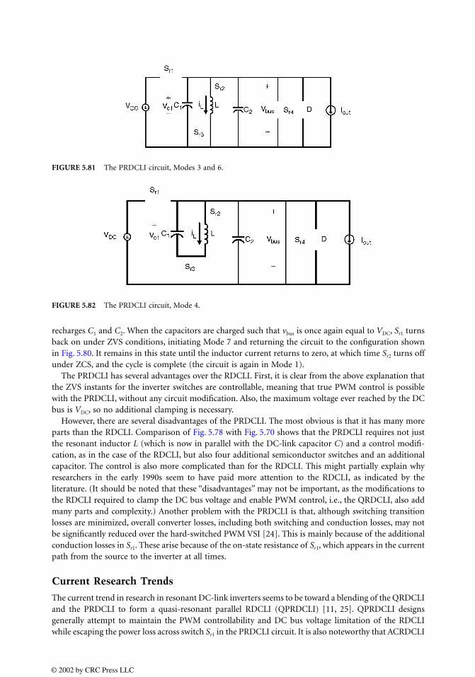
recharges C1 and C2. When the capacitors are charged such that vbus is once again equal to VDC, Sr1 turnsback on under ZVS conditions, initiating Mode 7 and returning the circuit to the configuration shownin Fig. 5.80. It remains in this state until the inductor current returns to zero, at which time Sr2 turns offunder ZCS, and the cycle is complete (the circuit is again in Mode 1).
The PRDCLI has several advantages over the RDCLI. First, it is clear from the above explanation thatthe ZVS instants for the inverter switches are controllable, meaning that true PWM control is possiblewith the PRDCLI, without any circuit modification. Also, the maximum voltage ever reached by the DCbus is VDC, so no additional clamping is necessary.
However, there are several disadvantages of the PRDCLI. The most obvious is that it has many moreparts than the RDCLI. Comparison of Fig. 5.78 with Fig. 5.70 shows that the PRDCLI requires not justthe resonant inductor L (which is now in parallel with the DC-link capacitor C) and a control modifi-cation, as in the case of the RDCLI, but also four additional semiconductor switches and an additionalcapacitor. The control is also more complicated than for the RDCLI. This might partially explain whyresearchers in the early 1990s seem to have paid more attention to the RDCLI, as indicated by theliterature. (It should be noted that these “disadvantages” may not be important, as the modifications tothe RDCLI required to clamp the DC bus voltage and enable PWM control, i.e., the QRDCLI, also addmany parts and complexity.) Another problem with the PRDCLI is that, although switching transitionlosses are minimized, overall converter losses, including both switching and conduction losses, may notbe significantly reduced over the hard-switched PWM VSI [24]. This is mainly because of the additionalconduction losses in Sr1. These arise because of the on-state resistance of Sr1, which appears in the currentpath from the source to the inverter at all times.
Current Research Trends
The current trend in research in resonant DC-link inverters seems to be toward a blending of the QRDCLIand the PRDCLI to form a quasi-resonant parallel RDCLI (QPRDCLI) [11, 25]. QPRDCLI designsgenerally attempt to maintain the PWM controllability and DC bus voltage limitation of the RDCLIwhile escaping the power loss across switch Sr1 in the PRDCLI circuit. It is also noteworthy that ACRDCLI
FIGURE 5.81 The PRDCLI circuit, Modes 3 and 6.
FIGURE 5.82 The PRDCLI circuit, Mode 4.
© 2002 by CRC Press LLC

technology has moved beyond the laboratory; ACRDCLIs with power ratings as high as 200 kVA werecommercially available as early as 1997 [26] and are already being used in uninterruptible power supplies,variable-speed drives, battery chargers, and several other products [27].
References
1. Mohan, N., Undeland, T., and Robbins, W., Power Electronics: Converters, Applications, and Design,2nd ed., John Wiley & Sons, New York, 1995.
2. Divan, D., The resonant DC link converter—a new concept in static power conversion, IEEE Trans.Ind. Appl., 25, 317, 1989.
3. Divan, D. and Skibinski, G., Zero-switching-loss inverters for high-power applications, IEEE Trans.Ind. Appl., 25, 634, 1989.
4. Hart, D.W., Introduction to Power Electronics, Prentice-Hall, Upper Saddle River, NJ, 1997, chap. 6.5. Hart, D.W., Introduction to Power Electronics, Prentice-Hall, Upper Saddle River, NJ, 1997, chap. 8.6. Divan, D.M., Venkataramanan, G., and DeDoncker, R.W.A.A., Design methodologies for soft switched
inverters, IEEE Trans. Ind. Appl., 29, 126, 1993.7. Rashid, M., Power Electronics: Circuits, Devices, and Applications, 2nd ed., Prentice-Hall, Upper
Saddle River, NJ, 1993.8. Garcia, P.D. and Barbi, I., A family of resonant DC-link voltage source inverters, in Transactions of
the IEEE Annual Conference on Industrial Electronics (IECON), 1990, 844.9. Divan, D. M., Malesani, L., Tenti, P., and Toigo, V., A synchronized resonant DC link converter for
soft-switched PWM, IEEE Trans. Ind. Appl., 29, 940, 1993.10. Venkataramanan, G. and Divan, D. M., Pulse width modulation with resonant DC link converters,
IEEE Trans. Ind. Appl., 29, 112, 1993.11. Kwon, K.-A., Kim, K.-H., Jung, Y.-C., and Park, M., New low-loss quasi-resonant DC link inverter
with lossless variable zero voltage duration, in Proceedings of the IEEE Annual Conference on IndustrialElectronics (IECON), 1997, 459.
12. Oh, I.-H., Jung, Y.-S., and Youn, M.-J., Source voltage-clamped resonant link inverter for a PMSMusing a predictive current control technique, IEEE Trans. Power Electron., 14, 1122, 1999.
13. Simonelli, J.M. and Torrey, D.A., Alternative bus clamp for resonant DC-link converters, IEEE Trans.Ind. Appl., 9, 56, 1994.
14. Dahono, P.A., Kataoka, T., and Sato, Y., New clamping circuits for resonant DC link inverters, inProceedings of the IEEE International Conference on Power Electronics, Drives, and Energy Systems forIndustrial Growth (PEDES), 1998, 833.
15. Venkataramanan, G., Divan, D., and Jahns, T., Discrete pulse modulation strategies for high-frequency inverter systems, IEEE Trans. Power Electron., 8, 279, 1993.
16. Kheraluwala, M.H. and Divan, D.M., Delta modulation strategies for resonant link inverters, IEEETrans. Power Electron., 5, 220, 1989.
17. Hui, S.Y.R., Gogani, E.S., and Zhang, J., Analysis of a quasi-resonant circuit for soft-switchedinverters, IEEE Trans. Power Electron., 11, 106, 1996.
18. Jafar, J.J. and Fernandes, B.G., Novel quasi-resonant DC-link PWM inverter for induction motordrive, in Record of the IEEE Annual Power Electronics Specialists Conference, 1999, 482.
19. Oh, I.-H. and Youn, M.-J., A simple soft-switched PWM inverter using source voltage clampedresonant circuit, IEEE Trans. Ind. Electron., 46, 468, 1999.
20. Ba-Thunya, A.S. and Toliyat, H.A., High frequency transformer assisted a new passive clamp ZVSquasi-resonant DC link PWM inverter with low voltage stress across the switches, in Record of theIEEE Annual Power Electronics Specialists Conference (PESC), 1999, 981.
21. Lee, J.-W., Sul, S.-K., and Park, M.-H., A novel three-phase quasi-resonant DC link inverter, in IEEEIndustry Applications Society Annual Meeting, 1992, 803.
22. Aoki, T., Nozaki, Y., and Kuwata, Y., Characteristics of a quasi-resonant DC link PWM inverter, inProceedings of the IEEE International Telecommunications Energy Conference (INTELEC), 1995, 602.
© 2002 by CRC Press LLC
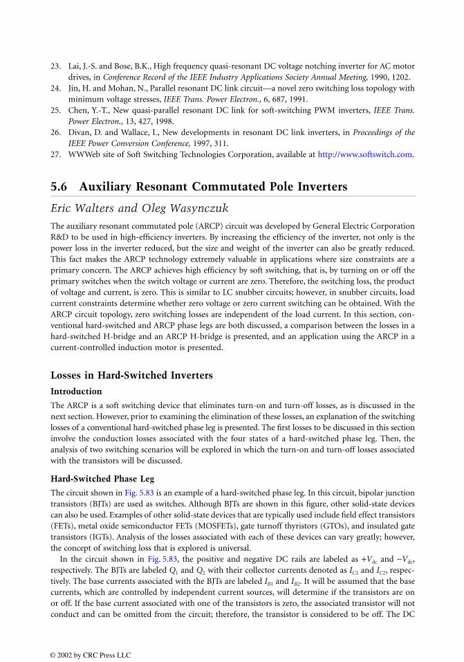
23. Lai, J.-S. and Bose, B.K., High frequency quasi-resonant DC voltage notching inverter for AC motordrives, in Conference Record of the IEEE Industry Applications Society Annual Meeting, 1990, 1202.
24. Jin, H. and Mohan, N., Parallel resonant DC link circuit—a novel zero switching loss topology withminimum voltage stresses, IEEE Trans. Power Electron., 6, 687, 1991.
25. Chen, Y.-T., New quasi-parallel resonant DC link for soft-switching PWM inverters, IEEE Trans.Power Electron., 13, 427, 1998.
26. Divan, D. and Wallace, I., New developments in resonant DC link inverters, in Proceedings of theIEEE Power Conversion Conference, 1997, 311.
27. WWWeb site of Soft Switching Technologies Corporation, available at http://www.softswitch.com.
5.6 Auxiliary Resonant Commutated Pole Inverters
Eric Walters and Oleg Wasynczuk
The auxiliary resonant commutated pole (ARCP) circuit was developed by General Electric CorporationR&D to be used in high-efficiency inverters. By increasing the efficiency of the inverter, not only is thepower loss in the inverter reduced, but the size and weight of the inverter can also be greatly reduced.This fact makes the ARCP technology extremely valuable in applications where size constraints are aprimary concern. The ARCP achieves high efficiency by soft switching, that is, by turning on or off theprimary switches when the switch voltage or current are zero. Therefore, the switching loss, the productof voltage and current, is zero. This is similar to LC snubber circuits; however, in snubber circuits, loadcurrent constraints determine whether zero voltage or zero current switching can be obtained. With theARCP circuit topology, zero switching losses are independent of the load current. In this section, con-ventional hard-switched and ARCP phase legs are both discussed, a comparison between the losses in ahard-switched H-bridge and an ARCP H-bridge is presented, and an application using the ARCP in acurrent-controlled induction motor is presented.
Losses in Hard-Switched Inverters
Introduction
The ARCP is a soft switching device that eliminates turn-on and turn-off losses, as is discussed in thenext section. However, prior to examining the elimination of these losses, an explanation of the switchinglosses of a conventional hard-switched phase leg is presented. The first losses to be discussed in this sectioninvolve the conduction losses associated with the four states of a hard-switched phase leg. Then, theanalysis of two switching scenarios will be explored in which the turn-on and turn-off losses associatedwith the transistors will be discussed.
Hard-Switched Phase Leg
The circuit shown in Fig. 5.83 is an example of a hard-switched phase leg. In this circuit, bipolar junctiontransistors (BJTs) are used as switches. Although BJTs are shown in this figure, other solid-state devicescan also be used. Examples of other solid-state devices that are typically used include field effect transistors(FETs), metal oxide semiconductor FETs (MOSFETs), gate turnoff thyristors (GTOs), and insulated gatetransistors (IGTs). Analysis of the losses associated with each of these devices can vary greatly; however,the concept of switching loss that is explored is universal.
In the circuit shown in Fig. 5.83, the positive and negative DC rails are labeled as +Vdc and −Vdc,respectively. The BJTs are labeled Q1 and Q2 with their collector currents denoted as IC1 and IC2, respec-tively. The base currents associated with the BJTs are labeled IB1 and IB2. It will be assumed that the basecurrents, which are controlled by independent current sources, will determine if the transistors are onor off. If the base current associated with one of the transistors is zero, the associated transistor will notconduct and can be omitted from the circuit; therefore, the transistor is considered to be off. The DC
© 2002 by CRC Press LLC
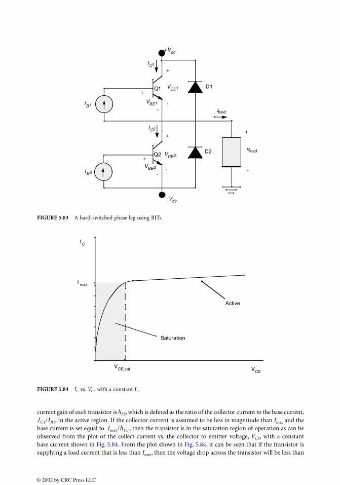
current gain of each transistor is hFE, which is defined as the ratio of the collector current to the base current,, in the active region. If the collector current is assumed to be less in magnitude than Imax and the
base current is set equal to , then the transistor is in the saturation region of operation as can beobserved from the plot of the collect current vs. the collector to emitter voltage, VCE, with a constantbase current shown in Fig. 5.84. From the plot shown in Fig. 5.84, it can be seen that if the transistor issupplying a load current that is less than Imax, then the voltage drop across the transistor will be less than
FIGURE 5.83 A hard-switched phase leg using BJTs.
FIGURE 5.84 IC vs. VCE with a constant IB.
IC1/IB1
Imax/hFE
© 2002 by CRC Press LLC

VCE,sat which is approximately 2 V for high-voltage BJTs. Therefore, the load voltage will be within 2 V ofthe potential of the DC rail to which the transistor is connected. Specifically,
(5.65)
If the source voltage is large compared to VCE,sat, i.e.,
(5.66)
then
(5.67)
The previous equations apply only when Q1 is on and the load current is positive. However, if the loadcurrent is negative and transistor Q2 is off, the only path for the current is through diode D1. In this case,
(5.68)
Typically, VD1 is on the order of 1 V, where
(5.69)
Thus,
(5.70)
It can be seen that the output voltage is approximately equal to Vdc when Q1 is on or when Q2 is off andthe load current is negative.
If transistor Q2 is on and the load current is negative
(5.71)
Hence,
(5.72)
With Q1 off and the load current positive, the load current must flow through diode D2. In this case,
(5.73)
Therefore,
(5.74)
Hence, when Q2 is on or when Q1 is off and the load current is positive, the load voltage is approximatelyequal to −Vdc.
The hard-switched phase leg has four states: (1) Q1 on and the load current is positive, (2) Q2 off andthe load current negative, (3) Q2 on and the load current is negative, and (4) Q1 off and the load currentpositive. In each of these states, the load current is flowing through one of the four solid-state devicescomposing the phase leg. With the conduction of current through these physical devices, there is anassociated power loss. This conduction power loss can be calculated for each state as the product of the
vload Vdc VCE , sat–=
Vdc >> VCE ,sat
vload Vdc≈
vload Vdc VD1+=
Vdc >> VD1
vload Vdc≈
vload VCE , sat Vdc–=
vload Vdc–≈
vload −Vdc VD2–=
vload Vdc–≈
© 2002 by CRC Press LLC

load current and the voltage across the device supplying the current. When Q1 is on and the load currentis positive, the conduction power loss is
(5.75)
With Q2 off and the load current negative, the load current flows through diode D1 and introduces aconduction power loss of
(5.76)
In the third state with Q2 on and a negative load current, the conduction loss is
(5.77)
When Q1 is off and the load current is positive, the conduction power loss associated with D2 is
(5.78)
Transistor Turn-On Losses
Two examples of switching losses are explored in this section. Both examples involve the load voltagebeing switched from the lower DC rail, −Vdc, to the upper DC rail, +Vdc. In the first example, the loadcurrent, iload, is assumed to be positive. In the second case, the load current is assumed to be negative.In both examples, the load is assumed to be inductive whereby the load current is essentially constantduring the switching interval.
It is assumed, initially, that the load is latched to the lower DC rail (transistor Q2 is on and Q1 is off)and the load current is positive. Although Q2 is gated on, the load current flows through the diode D2,whereupon a small conduction loss, PD2, is associated with D2. The value of diode conduction power lossis the product of the load current and the forward voltage drop across D1 (approximately 1 V). Theconduction energy loss for D2 can be calculated as the integral of the conduction power loss with respectto time, i.e.,
(5.79)
With all the load current flowing through the diode, the transistor Q2 will not have any conduction losses.Therefore, the only loss initially associated with this state of the phase leg is the conduction loss in thediode.
When the commutation process begins, transistor Q2 is turned off, and after a brief delay transistorQ1 is turned on. Since transistor Q2 is switched off under zero current conditions, there is no power lossassociated with Q2 in the turn-off process. However, when Q1 is turned on, the load current does notimmediately commute from diode D2 to Q1 because the minority carriers in the base region of Q1 mustbe supplied before conduction through Q1 can begin. As the base current, IB1, adds minority carriers tothe base of Q1, the collector current starts increasing and displacing the current through D2 as the sourceof the load current. This increase in the collector current can be observed in the simplified plots shownin Fig. 5.85. During this interval, both diode D2 and transistor Q1 are conducting; however, with D2
conducting, the load voltage is still clamped to the lower DC rail. This results in the rail-to-rail voltagebeing placed across Q1 while current is flowing through Q1; thus, a large amount of power is lost in Q1
during this phase of the commutation. This increase in the collector current, IC1, and the constant VCE1
can be observed in Fig. 5.85 [1]. The resulting power loss in Q1 during this interval is approximated asa straight line increasing to Pmax (Fig. 5.85). However, since current is also flowing through diode D2
during this interval, there is an additional loss term associated with the conduction of some of the loadcurrent through D2.
PQ1, con iload VCE , sat⋅=
PD1, con i– load VD1⋅=
PQ2,con iload– VCE ,sat⋅=
PD2,con iload VD2⋅=
ED2 PD2 t V=d∫ D2iload td∫=
© 2002 by CRC Press LLC
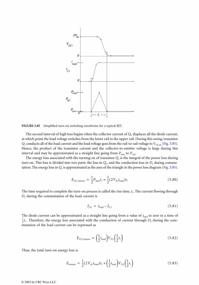
The second interval of high loss begins when the collector current of Q1 displaces all the diode current,at which point the load voltage switches from the lower rail to the upper rail. During this swing, transistorQ1 conducts all of the load current and the load voltage goes from the rail-to-rail voltage to VCE,sat (Fig. 5.85).Hence, the product of the transistor current and the collector-to-emitter voltage is large during thisinterval and may be approximated as a straight line going from Pmax to Pcon.
The energy loss associated with the turning on of transistor Q1 is the integral of the power loss duringturn-on. This loss is divided into two parts: the loss in Q1, and the conduction loss in D2 during commu-tation. The energy loss in Q1 is approximated as the area of the triangle in the power loss diagram (Fig. 5.85).
(5.80)
The time required to complete the turn-on process is called the rise time, tr . The current flowing throughD2 during the commutation of the load current is
(5.81)
The diode current can be approximated as a straight line going from a value of iload to zero in a time of. Therefore, the energy loss associated with the conduction of current through D2 during the com-
mutation of the load current can be expressed as
(5.82)
Thus, the total turn-on energy loss is
(5.83)
FIGURE 5.85 Simplified turn-on switching waveforms for a typical BJT.
IC1
VCE1
2Vdc
0
tr
iload
0
0
PQ1
Pmax
Pcon
EQ1,turnon12--Pmaxtr
12--= 2Vdciload( )tr=
ID2 iload IC1–=
12--tr
ED2,turnon12--iload
VD212--tr
=
Eturnon12-- 2Vdciload( )tr
12--iload
VD212--tr
+=
© 2002 by CRC Press LLC
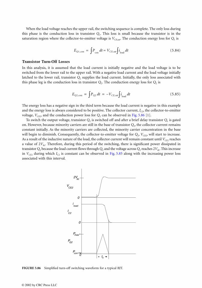
When the load voltage reaches the upper rail, the switching sequence is complete. The only loss duringthis phase is the conduction loss in transistor Q1. This loss is small because the transistor is in thesaturation region where the collector-to-emitter voltage is VCE,sat. The conduction energy loss for Q1 is
(5.84)
Transistor Turn-Off Losses
In this analysis, it is assumed that the load current is initially negative and the load voltage is to beswitched from the lower rail to the upper rail. With a negative load current and the load voltage initiallylatched to the lower rail, transistor Q2 supplies the load current. Initially, the only loss associated withthis phase leg is the conduction loss in transistor Q2. The conduction energy loss for Q2 is
(5.85)
The energy loss has a negative sign in the third term because the load current is negative in this exampleand the energy loss is always considered to be positive. The collector current, IC2, the collector-to-emittervoltage, VCE2, and the conduction power loss for Q2 can be observed in Fig. 5.86 [1].
To switch the output voltage, transistor Q2 is switched off and after a brief delay transistor Q1 is gatedon. However, because minority carriers are still in the base of transistor Q2, the collector current remainsconstant initially. As the minority carriers are collected, the minority carrier concentration in the basewill begin to diminish. Consequently, the collector-to-emitter voltage for Q2, VCE2, will start to increase.As a result of the inductive nature of the load, the collector current will remain constant until VCE2 reachesa value of 2Vdc. Therefore, during this period of the switching, there is significant power dissipated intransistor Q2 because the load current flows through Q2 and the voltage across Q2 reaches 2Vdc. This increasein VCE2 during which IC2 is constant can be observed in Fig. 5.85 along with the increasing power lossassociated with this interval.
FIGURE 5.86 Simplified turn-off switching waveform for a typical BJT.
EQ1,con P∫ contd VCE ,sat i∫ load
td≈=
EQ2,con PQ2 td∫ V– CE ,sat i∫ loadtd= =
IC2
VCE2
2Vdc
0
tc
iload
0
PQ2
Pmax
Pcon 0
© 2002 by CRC Press LLC

Once VCE2 reaches a value of 2Vdc, diode D1 becomes forward-biased and begins to assume part of theload current. This commutation of the load current from Q2 to D1 causes IC2 to decrease. During thisdecrease, large amounts of power are still being dissipated in transistor Q2. In addition, there is also apower loss associated with the conduction of current through diode D1.
The energy loss associated with the turn-off process of transistor Q2 is expressed as the sum of theenergy loss in Q2 and the conduction energy loss in D1 during the commutation of the load current fromQ2 to D1. The energy loss in Q2 can be approximated as the area of the triangle in the power loss diagramfor Q2 (Eq. 5.86), where tc is called the commutation time.
(5.86)
During the commutation of the load current, the diode current, ID1, can be expressed as
(5.87)
With a negative load current and IC1 going from a value of −iload to zero, the diode current can beapproximated as a straight line going from zero to iload. Therefore, the conduction energy loss associatedwith the commutation of the load current can be approximated as the product of the average diodecurrent, the forward diode voltage drop, and the time of the commutation, .
(5.88)
The total turn-off energy loss is
(5.89)
When all the load current is conducting through D1, the commutation of the load current from Q2 to D1
is complete. The only power loss in this final state of the switching sequence is the commutation lossassociated with diode D1. The conduction energy loss for D1 is
Analysis of ARCP Phase Leg
An analysis of an ARCP phase leg is presented in this section. This analysis begins with a description ofthe ARCP circuit. The switching of the load voltage from the lower rail to the upper rail is then exploredfor three separate cases: (1) commutation from a diode, (2) commutation from a transistor with low loadcurrent, and (3) commutation from a transistor with high load current. The elimation of the switchinglosses is discussed in each case.
ARCP Circuit Description
A circuit diagram of the ARCP phase leg is illustrated in Fig. 5.87 [2]. The ARCP contains snubbercapacitors Cr between the load and the DC rails. The snubber capacitors serve the purpose of holdingthe voltage across the switches constant during turn-off. This makes it possible for the switch beingturned-off to have zero voltage across it during turn-off, thus eliminating switching losses. The ARCPalso includes an auxiliary circuit connected between the DC neutral and phase connection. The auxiliarycircuit helps enable the load to be swung to the opposite rail to ensure zero turn-on voltage. If theauxiliary circuit is not included, then there is a load current constraint to ensure zero turn-on voltage.
EQ2,turnoff12-- Pmax tc⋅( ) 1
2-- 2Vdciload( )tc–==
ID1 IC1 iload–=
12--tc
ED1,turnoff12--– iload
VD112--tc
=
Eturnoff12-- 2Vdciload( )tc– 1
2--– iload
VD112--tc
+=
ED1,con PD1 td∫ V– D1 i∫ loadtd= =
© 2002 by CRC Press LLC
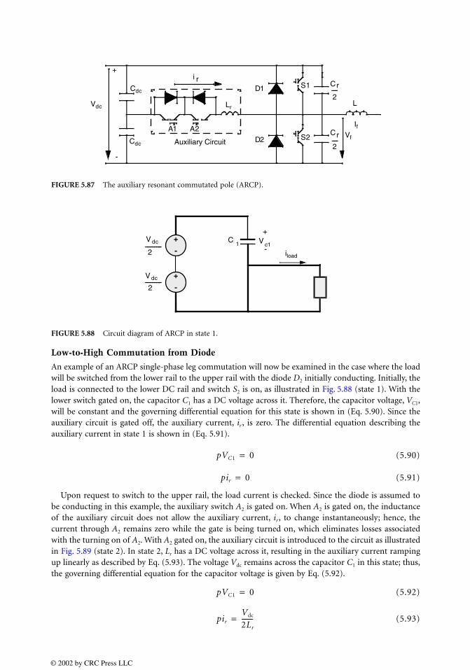
Low-to-High Commutation from Diode
An example of an ARCP single-phase leg commutation will now be examined in the case where the loadwill be switched from the lower rail to the upper rail with the diode D2 initially conducting. Initially, theload is connected to the lower DC rail and switch S2 is on, as illustrated in Fig. 5.88 (state 1). With thelower switch gated on, the capacitor C1 has a DC voltage across it. Therefore, the capacitor voltage, VC1,will be constant and the governing differential equation for this state is shown in (Eq. 5.90). Since theauxiliary circuit is gated off, the auxiliary current, ir , is zero. The differential equation describing theauxiliary current in state 1 is shown in (Eq. 5.91).
(5.90)
(5.91)
Upon request to switch to the upper rail, the load current is checked. Since the diode is assumed tobe conducting in this example, the auxiliary switch A2 is gated on. When A2 is gated on, the inductanceof the auxiliary circuit does not allow the auxiliary current, ir , to change instantaneously; hence, thecurrent through A2 remains zero while the gate is being turned on, which eliminates losses associatedwith the turning on of A2. With A2 gated on, the auxiliary circuit is introduced to the circuit as illustratedin Fig. 5.89 (state 2). In state 2, Lr has a DC voltage across it, resulting in the auxiliary current rampingup linearly as described by Eq. (5.93). The voltage Vdc remains across the capacitor C1 in this state; thus,the governing differential equation for the capacitor voltage is given by Eq. (5.92).
(5.92)
(5.93)
FIGURE 5.87 The auxiliary resonant commutated pole (ARCP).
FIGURE 5.88 Circuit diagram of ARCP in state 1.
A1 A2
+
-
Auxiliary Circuit
D1
D2
S1
S2
Vdc
Cdc
Cdc
i rCr
2-----
Cr
2-----
Vf
If
L Lr
pVC1 0=
pir 0=
pVC1 0=
pir
Vdc
2Lr
-------=
© 2002 by CRC Press LLC
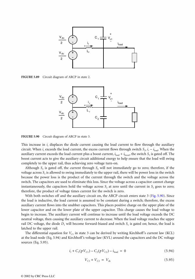
This increase in ir displaces the diode current causing the load current to flow through the auxiliarycircuit. When ir exceeds the load current, the excess current flows through switch S2, ir − iload. When theauxiliary current exceeds the load current plus a boost current, iload + iboost, the switch S2 is gated off. Theboost current acts to give the auxiliary circuit additional energy to help ensure that the load will swingcompletely to the upper rail, thus achieving zero voltage turn-on.
Although S2 is gated off, the current through S2 will not immediately go to zero; therefore, if thevoltage across S2 is allowed to swing immediately to the upper rail, there will be power loss in the switchbecause the power loss is the product of the current through the switch and the voltage across theswitch. The capacitors are used to eliminate this loss. Since the voltage across a capacitor cannot changeinstantaneously, the capacitors hold the voltage across S2 at zero until the current in S2 goes to zero;therefore, the product of voltage times current for the switch is zero.
With both switches off and the auxiliary circuit on, the ARCP circuit enters state 3 (Fig. 5.90). Sincethe load is inductive, the load current is assumed to be constant during a switch; therefore, the excessauxiliary current flows into the snubber capacitors. This places positive charge on the upper plate of thelower capacitor and on the lower plate of the upper capacitor. This charge causes the load voltage tobegin to increase. The auxiliary current will continue to increase until the load voltage exceeds the DCneutral voltage, then causing the auxiliary current to decrease. When the load voltage reaches the upperrail DC voltage, the diode D1 will become forward-biased and switch S1 is gated on; hence, the load islatched to the upper rail.
The differential equation for VC1 in state 3 can be derived by writing Kirchhoff ’s current law (KCL)at the load node (Eq. 5.94) and Kirchhoff ’s voltage law (KVL) around the capacitors and the DC voltagesources (Eq. 5.95).
(5.94)
(5.95)
FIGURE 5.89 Circuit diagram of ARCP in state 2.
FIGURE 5.90 Circuit diagram of ARCP in state 3.
ir C1 pVC1( ) C2 pVC2( )– iload–+ 0=
VC1 VC2+ Vdc=
© 2002 by CRC Press LLC

A relationship between and c.an be established (Eqs. 5.96 and 5.97) by taking the derivativeof both sides of Eq. (3–6).
(5.96)
(5.97)
Substituting Eq. (5.97) into Eq. (5.94) and simplifying yields the differential equation for VC1 shownin Eq. (5.99). The differential equation describing ir in state 3 can be derived by simplifying the KVLequation around the loop including the auxiliary circuit, C1, and the upper DC voltage source (Eqs. 5.98and 5.100).
(5.98)
(5.99)
(5.100)
When diode D1 is forward-biased and switch S1 is gated on, the snubber capacitors ensure that thevoltage across S1 remains zero, thereby eliminating any turn-on loss in switch S1. With the load latchedto the upper rail, the auxiliary circuit has a negative voltage across it. Therefore, the auxiliary currentwill linearly ramp down as described by Eq. (5.102). With switch S1 gated on, the capacitor voltage VC1
is held at zero; thus, the derivative of the capacitor voltage will also be zero (Eq. 5.101).
(5.101)
(5.102)
When the auxiliary current reaches zero, switch A2 is gated off. Since the current through A2 is zerowhen switch A2 is gated off, there is no switching losses associated with A2.
When A2 is gated off, the auxiliary circuit is taken off the circuit and the final state is reached with theload latched to the upper rail. With the auxiliary circuit removed, the auxiliary current is zero; hence,the derivative of the auxiliary current will also be zero Eq. (5.104). Since switch S1 is still latched on, thederivative of the capacitor voltage will remain zero Eq. (5.103).
(5.103)
(5.104)
A computer-simulated plot of the upper capacitor voltage VC1 and the auxiliary current ir is shown inFig. 5.93 for a switch from low to high with the diode initially conducting. The ARCP parameter valuesused in the simulation were derived from Ref. 2 and are listed in Table 5.3.
The computer code used in the simulation was written in Advanced Continuous Simulation Language(ACSL). From the graph, the individual switching states can be observed along with the transition points
pVC1 pVC2
p VC1 VC2+( ) pVdc 0= =
pVC1 p– VC2=
Vdc
2------- Lr pir( ) VC1–+ 0=
pVC1
iload ir–C1 C2+------------------=
pir
VC1
Vdc
2-------–
Lr
----------------------=
pVC1 0=
pir
Vdc
2Lr
-------–=
pVC1 0=
pir 0=
© 2002 by CRC Press LLC
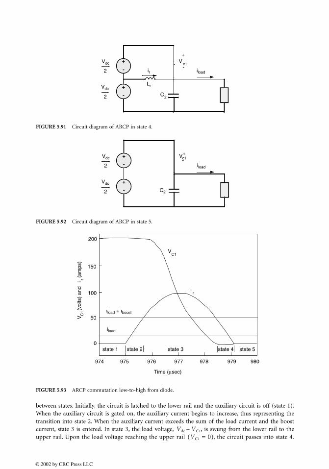
between states. Initially, the circuit is latched to the lower rail and the auxiliary circuit is off (state 1).When the auxiliary circuit is gated on, the auxiliary current begins to increase, thus representing thetransition into state 2. When the auxiliary current exceeds the sum of the load current and the boostcurrent, state 3 is entered. In state 3, the load voltage, , is swung from the lower rail to theupper rail. Upon the load voltage reaching the upper rail , the circuit passes into state 4.
FIGURE 5.91 Circuit diagram of ARCP in state 4.
FIGURE 5.92 Circuit diagram of ARCP in state 5.
FIGURE 5.93 ARCP commutation low-to-high from diode.
state 1 state 5state 4state 3state 20
50
100
150
200
975 979978977976 980974
Time (µsec)
iload
iload + iboost
ir
VC1
VC
1i r
(vol
ts)
and
(
amps
)
Vdc VC1–VC1 0=( )
© 2002 by CRC Press LLC

In state 4, the auxiliary current decreases linearly. When the auxiliary current equals zero, state 5 is reached.The capacitor voltage, , is not constant during states 2 and 4 as discussed earlier because in thesimulation the diodes and switches were not modeled as ideal; thus, a small deviation was introduced.
Low-to-High Commutation from Switch, Low Current
In the second example of an ARCP single-leg commutation, it is assumed that the load voltage is to beswitched from the lower to upper rail with switch S2 initially conducting a small current. The governingdifferential equations describing each state are the same as in the previous example.
Initially, the load is latched to the lower rail (state 1). When the ARCP phase leg is commanded toswitch to the upper rail, the load current is checked. Since the load current is assumed to be flowingthrough the switch, the magnitude of the current is compared with a threshold value. In this case, it isassumed that the current is less than the threshold value; therefore, the load does not contain enoughenergy to overcome losses to drive the load to the opposite rail without the introduction of the auxiliarycircuit. Thus, the auxiliary circuit is turned on by gating switch A2 on.
With the auxiliary circuit gated on, the circuit is in state 2. The auxiliary current will ramp up becauseof the DC voltage placed across it. When the auxiliary current reaches the value of the boost current plusthe load current, the auxiliary circuit has substantial energy to drive the load to the opposite rail. Therefore,the lower switch, S2, is gated off. The snubber capacitors prevent switching losses in S2 because the capacitorshold the voltage across the switch to zero while the switch current diminishes.
State 3 is entered after turning off switch S2. The load current and the auxiliary current will chargethe snubber capacitors, hence driving the load voltage to the upper rail. When the load voltage reachesthe upper rail, the diode D1 will become forward-biased and will stop further charging of the capacitorsby conducting the excess current. When the diode becomes forward-biased, the switch S1 is gated onwith zero volts across the switch, thereby preventing any turn-on losses in S1.
When the load voltage is equal to the upper rail, state 4 (Fig. 5.91) is obtained. The auxiliary circuit hasa negative voltage across it. Therefore, the auxiliary current will ramp down. When the auxiliary currentreaches zero, switch A2 is gated off to disconnect the auxiliary circuit. With zero current through A2 duringturn-off, switching losses associated with A2 are avoided. The load is now latched to the upper rail and theauxiliary circuit is removed; therefore, the commutation is completed and the final state, state 5, is reached.
The upper capacitor voltage, VC1, and the auxiliary circuit, ir , are plotted in Fig. 5.94 for commutationfrom the switch in the low-current case. Commutation from the switch at low current levels is similarto commutation from the diode except that the auxiliary current does not have to become as large inthe switch example. This is because the load current aids the commutation process when the switch isinitially conducting and hinders commutation when the diode is initially conducting.
Low-to-High Commutation from Switch, High Current
The final case to be explored involves switching of the load from the lower to upper rail with the switchinitially conducting a current larger than the threshold current. Initially, the load is latched to the lowerrail and the circuit is in state 1 (Fig. 5.88). For a switch from the lower rail to the upper rail when switchS2 is conducting a current larger than the threshold value, the auxiliary circuit does not need to beincluded in the switching sequence. This is a result of the load inductor having sufficient energy to
TABLE 5.3 ARCP Parameters
ARCP Parameter Value Used in Simulation
Upper capacitor, C1 0.159 µFLower capacitor, C2 0.159 µFResonant inductor, Lr 0.159 µHThreshold current, ith 60 ABoost current, iboost 30 ARail-to-rail voltage, Vdc 200 V
VC1
© 2002 by CRC Press LLC
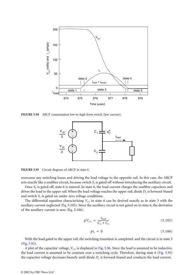
overcome any switching losses and driving the load voltage to the opposite rail. In this case, the ARCPacts exactly like a snubber circuit, because switch S2 is gated off without introducing the auxiliary circuit.
Once S2 is gated off, state 6 is entered. In state 6, the load current charges the snubber capacitors anddrives the load to the upper rail. When the load voltage reaches the upper rail, diode D1 is forward-biasedand switch S1 is gated on under zero voltage conditions.
The differential equation characterizing VC1 in state 6 can be derived exactly as in state 3 with theauxiliary current neglected (Eq. 5.105). Since the auxiliary circuit is not gated on in state 6, the derivativeof the auxiliary current is zero (Eq. 5.106).
(5.105)
(5.106)
With the load gated to the upper rail, the switching transition is completed. and the circuit is in state 5(Fig. 5.92).
A plot of the capacitor voltage, VC1, is displayed in Fig. 5.96. Since the load is assumed to be inductive,the load current is assumed to be constant over a switching cycle. Therefore, during state 6 (Fig. 5.95)the capacitor voltage decreases linearly until diode D1 is forward-biased and conducts the load current.
FIGURE 5.94 ARCP commutation low-to-high from switch (low current).
FIGURE 5.95 Circuit diagram of ARCP in state 6.
state 1 state 5
state 4
state 3
state 2
0
50
100
150
200
975 979978977976974
Time (µsec)
i
iload + iboost
load
i r
VC1
VC
1i r
(vol
ts)
and
(
amps
)
pVC1
iload
C1 C2+------------------=
pir 0=
© 2002 by CRC Press LLC
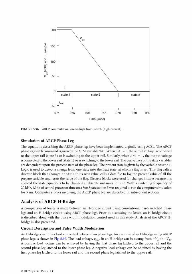
Simulation of ARCP Phase Leg
The equations describing the ARCP phase leg have been implemented digitally using ACSL. The ARCPphase leg switch command is given by the ACSL variable SW1. When SW1 = 5, the output voltage is connectedto the upper rail (state 5) or is switching to the upper rail. Similarly, when SW1 = 1, the output voltageis connected to the lower rail (state 1) or is switching to the lower rail. The derivatives of the state variablesare dependent upon the present state of the phase leg. The present state is given by the variable state1.Logic is used to detect a change from one state into the next state, at which a flag is set. This flag calls adiscrete block that changes state1 to its new value, calls a data file to log the present value of all theprepare variable, and resets the value of the flag. Discrete blocks were used for changes in state because thisallowed the state equations to be changed at discrete instances in time. With a switching frequency of20 kHz, 1.36 s of central processor time on a Sun Sparcstation 5 was required to run the computer simulationfor 5 ms. Computer studies involving the ARCP phase leg are described in subsequent sections.
Analysis of ARCP H-Bridge
A comparison of losses is made between an H-bridge circuit using conventional hard-switched phaselegs and an H-bridge circuit using ARCP phase legs. Prior to discussing the losses, an H-bridge circuitis discribed along with the pulse width modulation control used in this study. Analysis of the ARCP H-bridge is also presented.
Circuit Description and Pulse Width Modulation
An H-bridge circuit is a load connected between two phase legs. An example of an H-bridge using ARCPphase legs is shown in Fig. 5.97. The load voltage, vload, in an H-bridge can be swung from +Vdc to −Vdc.A positive load voltage can be achieved by having the first phase leg latched to the upper rail and thesecond phase leg latched to the lower phase leg. A negative load voltage can be obtained by having thefirst phase leg latched to the lower rail and the second phase leg latched to the upper rail.
FIGURE 5.96 ARCP commutation low-to-high from switch (high current).
state 1 state 5state 60
50
100
150
200
975 979978977976974
Time (µsec)
iload
ir
VC1
VC
1i r
(vol
ts)
and
(
amps
)
-50
980
© 2002 by CRC Press LLC
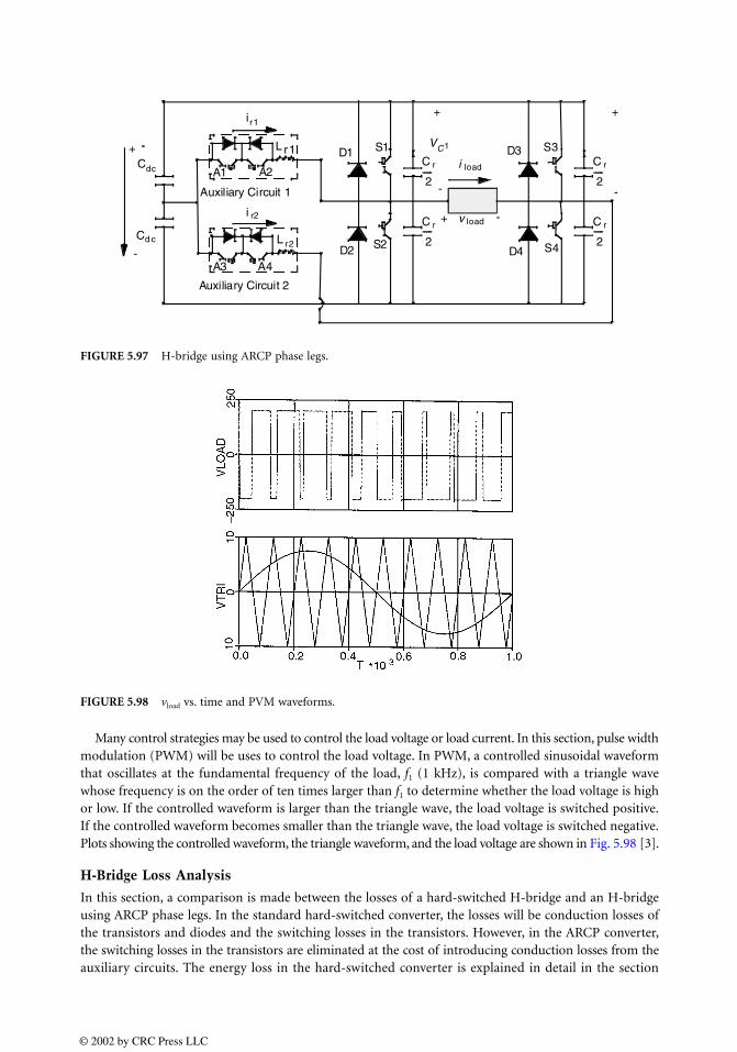
Many control strategies may be used to control the load voltage or load current. In this section, pulse widthmodulation (PWM) will be uses to control the load voltage. In PWM, a controlled sinusoidal waveformthat oscillates at the fundamental frequency of the load, f1 (1 kHz), is compared with a triangle wavewhose frequency is on the order of ten times larger than f1 to determine whether the load voltage is highor low. If the controlled waveform is larger than the triangle wave, the load voltage is switched positive.If the controlled waveform becomes smaller than the triangle wave, the load voltage is switched negative.Plots showing the controlled waveform, the triangle waveform, and the load voltage are shown in Fig. 5.98 [3].
H-Bridge Loss Analysis
In this section, a comparison is made between the losses of a hard-switched H-bridge and an H-bridgeusing ARCP phase legs. In the standard hard-switched converter, the losses will be conduction losses ofthe transistors and diodes and the switching losses in the transistors. However, in the ARCP converter,the switching losses in the transistors are eliminated at the cost of introducing conduction losses from theauxiliary circuits. The energy loss in the hard-switched converter is explained in detail in the section
FIGURE 5.97 H-bridge using ARCP phase legs.
FIGURE 5.98 vload vs. time and PVM waveforms.
© 2002 by CRC Press LLC
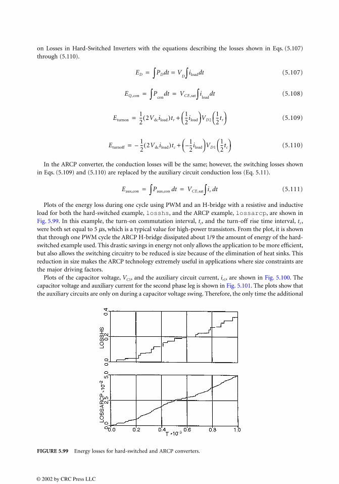
on Losses in Hard-Switched Inverters with the equations describing the losses shown in Eqs. (5.107)through (5.110).
(5.107)
(5.108)
(5.109)
(5.110)
In the ARCP converter, the conduction losses will be the same; however, the switching losses shownin Eqs. (5.109) and (5.110) are replaced by the auxiliary circuit conduction loss (Eq. 5.11).
(5.111)
Plots of the energy loss during one cycle using PWM and an H-bridge with a resistive and inductiveload for both the hard-switched example, losshs, and the ARCP example, lossarcp, are shown inFig. 5.99. In this example, the turn-on commutation interval, tc, and the turn-off rise time interval, tr ,were both set equal to 5 µs, which is a typical value for high-power transistors. From the plot, it is shownthat through one PWM cycle the ARCP H-bridge dissipated about 1/9 the amount of energy of the hard-switched example used. This drastic savings in energy not only allows the application to be more efficient,but also allows the switching circuitry to be reduced is size because of the elimination of heat sinks. Thisreduction in size makes the ARCP technology extremely useful in applications where size constraints arethe major driving factors.
Plots of the capacitor voltage, VC1, and the auxiliary circuit current, ir1, are shown in Fig. 5.100. Thecapacitor voltage and auxiliary current for the second phase leg is shown in Fig. 5.101. The plots show thatthe auxiliary circuits are only on during a capacitor voltage swing. Therefore, the only time the additional
FIGURE 5.99 Energy losses for hard-switched and ARCP converters.
ED PD t V=d∫ Diload td∫=
EQ ,con P∫ contd VCE ,sat i∫ load
td= =
Eturnon12-- 2Vdciload( )tr
12--iload
VD212--tr
+=
Eturnoff12-- 2Vdciload( )tc– 1
2--– iload
VD112--tc
+=
Eaux,con Paux,con td∫ VCE ,sat ir td∫= =
© 2002 by CRC Press LLC
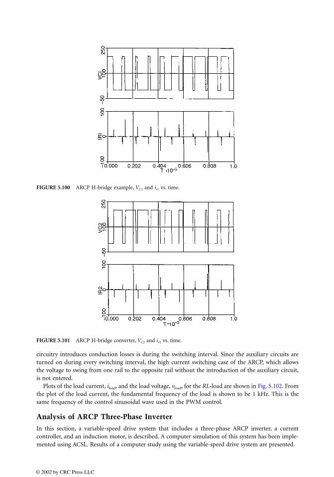
circuitry introduces conduction losses is during the switching interval. Since the auxiliary circuits areturned on during every switching interval, the high current switching case of the ARCP, which allowsthe voltage to swing from one rail to the opposite rail without the introduction of the auxiliary circuit,is not entered.
Plots of the load current, iload, and the load voltage, vload, for the RL-load are shown in Fig. 5.102. Fromthe plot of the load current, the fundamental frequency of the load is shown to be 1 kHz. This is thesame frequency of the control sinusoidal wave used in the PWM control.
Analysis of ARCP Three-Phase Inverter
In this section, a variable-speed drive system that includes a three-phase ARCP inverter, a currentcontroller, and an induction motor, is described. A computer simulation of this system has been imple-mented using ACSL. Results of a computer study using the variable-speed drive system are presented.
FIGURE 5.100 ARCP H-bridge example, VC1 and ir1 vs. time.
FIGURE 5.101 ARCP H-bridge converter, VC2 and ir2 vs. time.
© 2002 by CRC Press LLC
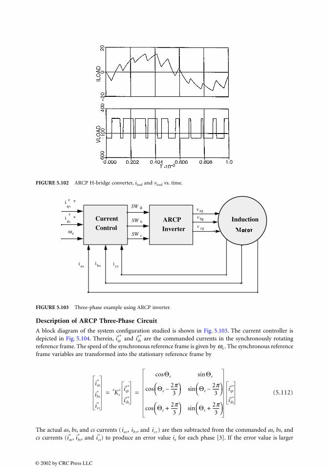
Description of ARCP Three-Phase Circuit
A block diagram of the system configuration studied is shown in Fig. 5.103. The current controller isdepicted in Fig. 5.104. Therein, and are the commanded currents in the synchronously rotatingreference frame. The speed of the synchronous reference frame is given by . The synchronous referenceframe variables are transformed into the stationary reference frame by
(5.112)
The actual as, bs, and cs currents ( , , and ) are then subtracted from the commanded as, bs, andcs currents ( , , and ) to produce an error value iε for each phase [3]. If the error value is larger
FIGURE 5.102 ARCP H-bridge converter, iload and vload vs. time.
FIGURE 5.103 Three-phase example using ARCP inverter.
iqse∗ ids
e∗
ωe
ias∗
ibs∗
ics∗
Ke s
siqs
e∗
idse∗
Θecos Θesin
Θe2π3
------– cos Θe
2π3
------– sin
Θe2π3
------+ cos Θe
2π3
------+ sin
iqse∗
idse∗
= =
ias ibs ics
ias∗ ibs
∗ ics∗
© 2002 by CRC Press LLC
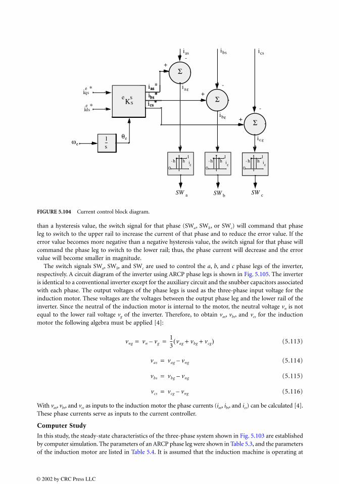
than a hysteresis value, the switch signal for that phase (SWa, SWb, or SWc) will command that phaseleg to switch to the upper rail to increase the current of that phase and to reduce the error value. If theerror value becomes more negative than a negative hysteresis value, the switch signal for that phase willcommand the phase leg to switch to the lower rail; thus, the phase current will decrease and the errorvalue will become smaller in magnitude.
The switch signals SWa, SWb, and SWc are used to control the a, b, and c phase legs of the inverter,respectively. A circuit diagram of the inverter using ARCP phase legs is shown in Fig. 5.105. The inverteris identical to a conventional inverter except for the auxiliary circuit and the snubber capacitors associatedwith each phase. The output voltages of the phase legs is used as the three-phase input voltage for theinduction motor. These voltages are the voltages between the output phase leg and the lower rail of theinverter. Since the neutral of the induction motor is internal to the motor, the neutral voltage vn is notequal to the lower rail voltage vg of the inverter. Therefore, to obtain vas, vbs, and vcs for the inductionmotor the following algebra must be applied [4]:
(5.113)
(5.114)
(5.115)
(5.116)
With vas, vbs, and vcs as inputs to the induction motor the phase currents (ias, ibs, and ics) can be calculated [4].These phase currents serve as inputs to the current controller.
Computer Study
In this study, the steady-state characteristics of the three-phase system shown in Fig. 5.103 are establishedby computer simulation. The parameters of an ARCP phase leg were shown in Table 5.3, and the parametersof the induction motor are listed in Table 5.4. It is assumed that the induction machine is operating at
FIGURE 5.104 Current control block diagram.
vng vn vg–= 13-- vag vbg vcg+ +( )=
vas vag vng–=
vbs vbg vng–=
vcs vcg vng–=
© 2002 by CRC Press LLC
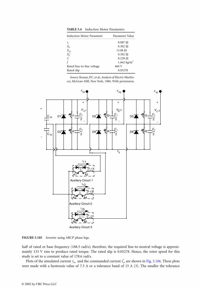
half of rated or base frequency (188.5 rad/s); therefore, the required line-to-neutral voltage is approxi-mately 133 V rms to produce rated torque. The rated slip is 0.05278. Hence, the rotor speed for thisstudy is set to a constant value of 178.6 rad/s.
Plots of the simulated current and the commanded current are shown in Fig. 5.106. These plotswere made with a hysteresis value of 7.5 A or a tolerance band of 15 A [3]. The smaller the tolerance
TABLE 5.4 Induction Motor Parameters
Induction Motor Parameter Parameter Value
rs 0.087 ΩXls 0.302 ΩXM 13.08 ΩXlr′ 0.302 Ωrr′ 0.228 ΩJ 1.662 kg/m
2
Rated line-to-line voltage 460.VRated slip 0.05278
Source: Krause, P.C. et al., Analysis of Electric Machin-ery, McGraw-Hill, New York, 1986. With permission.
FIGURE 5.105 Inverter using ARCP phase legs.
L r3
D3
D4
S3
S4
C r
2-----
C r
2-----
+
-
C dc
C dc
A3 A4
Auxiliary Circuit 2
ir2
L r2
A1 A2
Auxiliary Circuit 1
ir1
L r1
D5
D6
S5
S6
Cr
2-----
Cr
2-----
VC 2
+ +
- -
D1
D2
S1
S2
Cr
2-----
Cr
2-----
VC1
+
-
A5 A6
Auxiliary Circuit 3
i r3
VC 3
vag vbg
vg
vcg
ias ias∗
© 2002 by CRC Press LLC
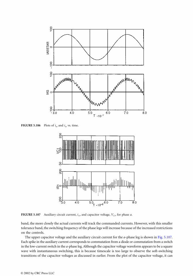
band, the more closely the actual currents will track the commanded currents. However, with this smallertolerance band, the switching frequency of the phase legs will increase because of the increased restrictionson the controls.
The upper capacitor voltage and the auxiliary circuit current for the a-phase leg is shown in Fig. 5.107.Each spike in the auxiliary current corresponds to commutation from a diode or commutation from a switchin the low-current switch in the a-phase leg. Although the capacitor voltage waveform appears to be a squarewave with instantaneous switching, this is because timescale is too large to observe the soft-switchingtransitions of the capacitor voltages as discussed in earlier. From the plot of the capacitor voltage, it can
FIGURE 5.106 Plots of ias and ias vs. time.
FIGURE 5.107 Auxiliary circuit current, ir1, and capacitor voltage, VC1, for phase a.
© 2002 by CRC Press LLC
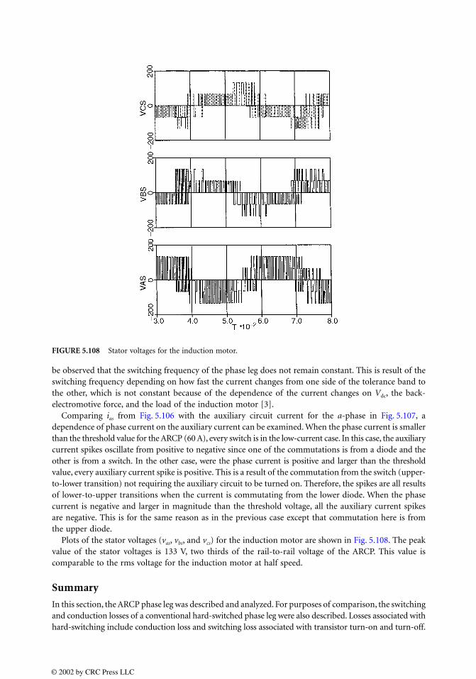
be observed that the switching frequency of the phase leg does not remain constant. This is result of theswitching frequency depending on how fast the current changes from one side of the tolerance band tothe other, which is not constant because of the dependence of the current changes on Vdc, the back-electromotive force, and the load of the induction motor [3].
Comparing ias from Fig. 5.106 with the auxiliary circuit current for the a-phase in Fig. 5.107, adependence of phase current on the auxiliary current can be examined. When the phase current is smallerthan the threshold value for the ARCP (60 A), every switch is in the low-current case. In this case, the auxiliarycurrent spikes oscillate from positive to negative since one of the commutations is from a diode and theother is from a switch. In the other case, were the phase current is positive and larger than the thresholdvalue, every auxiliary current spike is positive. This is a result of the commutation from the switch (upper-to-lower transition) not requiring the auxiliary circuit to be turned on. Therefore, the spikes are all resultsof lower-to-upper transitions when the current is commutating from the lower diode. When the phasecurrent is negative and larger in magnitude than the threshold voltage, all the auxiliary current spikesare negative. This is for the same reason as in the previous case except that commutation here is fromthe upper diode.
Plots of the stator voltages (vas, vbs, and vcs) for the induction motor are shown in Fig. 5.108. The peakvalue of the stator voltages is 133 V, two thirds of the rail-to-rail voltage of the ARCP. This value iscomparable to the rms voltage for the induction motor at half speed.
Summary
In this section, the ARCP phase leg was described and analyzed. For purposes of comparison, the switchingand conduction losses of a conventional hard-switched phase leg were also described. Losses associated withhard-switching include conduction loss and switching loss associated with transistor turn-on and turn-off.
FIGURE 5.108 Stator voltages for the induction motor.
© 2002 by CRC Press LLC

In an ARCP phase leg, all switching losses are eliminated by turning transistors on and off under eitherzero current or zero voltage conditions. This is accomplished with the introduction of anauxiliary circuitthat aids the commutation process. With the switching losses eliminated, the only losses in an ARCPphase leg involve the conduction losses in the phase leg and in the auxiliary circuit.
The switching sequence of the ARCP and the corresponding state equations are described in detail inthis section. Based on these state equations, computer models of the ARCP and hard-switched phase legswere developed and implemented using ACSL.
A computer study was performed to compare the losses of ARCP and hard-switched switching strat-egies. In the study, an H-bridge using conventional PWM was analyzed using both types of phase legsand a comparison was made between the energy loss in both cases. It was shown that the ARCP, byeliminating switching losses, used approximately 1/9 the energy per PWM cycle of the hard-switchedconverter.
Finally, a variable-speed induction motor drive system using a three-phase ARCP inverter was simu-lated. The dependence of the auxiliary current of an ARCP phase leg on the phase current was presentedalong with a discussion on the relationship between current control parameters and switching frequency.
References
1. R. E. Tarter, Principles of Solid-State Power Conversion, Howard W. Sams & Co., Indianapolis, IN,1985, 68–76.
2. R. W. DeDoncker, Resonant pole converters, presented at EPE-1993, 4.1–4.45.3. N. Mohan, T. M. Undeland, and W. P. Robbins, Power Electronics: Converters, Applications, and Design,
John Wiley & Sons, New York, 1989, 104–121, 146–148. 4. P. C. Krause, O. Wasynczuk, and S. D. Sudhoff, Analysis of Electric Machinery, McGraw-Hill, New York,
1986.
© 2002 by CRC Press LLC

6Multilevel Converters
6.1 Introduction6.2 Multilevel Voltage Source Modulation6.3 Fundamental Multilevel Converter Topologies
Diode-Clamped Multilevel Converters • Flying-Capacitor Multilevel Converters • Cascaded H-Bridge Multilevel Converters • Multilevel H-Bridge Converters
6.4 Cascaded Multilevel Converter TopologiesCascaded Multilevel Converters • Cascaded Multilevel H-Bridge Converters
6.5 Multilevel Converter Laboratory ExamplesThree-Level Diode-Clamped Inverter • The Cascade-3/2 Inverter • The Cascade-5/3H Inverter
6.6 Conclusion
6.1 Introduction
Multilevel power conversion was first introduced 20 years ago [1]. The general concept involves utilizinga higher number of active semiconductor switches to perform the power conversion in small voltagesteps. There are several advantages to this approach when compared with traditional (two-level) powerconversion. The smaller voltage steps lead to the production of higher power quality waveforms and alsoreduce the dv/dt stresses on the load and reduce the electromagnetic compatibility (EMC) concerns.Another important feature of multilevel converters is that the semiconductors are wired in a series-typeconnection, which allows operation at higher voltages. However, the series connection is typically madewith clamping diodes, which eliminates overvoltage concerns. Furthermore, since the switches are nottruly series connected, their switching can be staggered, which reduces the switching frequency and thusthe switching losses.
One clear disadvantage of multilevel power conversion is the larger number of semiconductor switchesrequired. It should be pointed out that lower voltage rated switches can be used in the multilevel converterand therefore the active semiconductor cost is not appreciably increased when compared with the two-level case. However, each active semiconductor added requires associated gate drive circuitry and addsfurther complexity to the converter mechanical layout. Another disadvantage of multilevel power con-verters is that the small voltage steps are typically produced by isolated voltage sources or a bank of seriescapacitors. Isolated voltage sources may not always be readily available and series capacitors requirevoltage balance. To some extent, the voltage balancing can be addressed by using redundant switchingstates, which exist due to the high number of semiconductor devices. However, for a complete solutionto the voltage-balancing problem, another multilevel converter may be required [2–4].
In recent years, there has been a substantial increase in interest in multilevel power conversion. Thisis evident by the fact that some Institute of Electrical and Electronic Engineers (IEEE) conferences are
Keith CorzineUniversity of Wisconsin–Milwaukee
© 2002 by CRC Press LLC
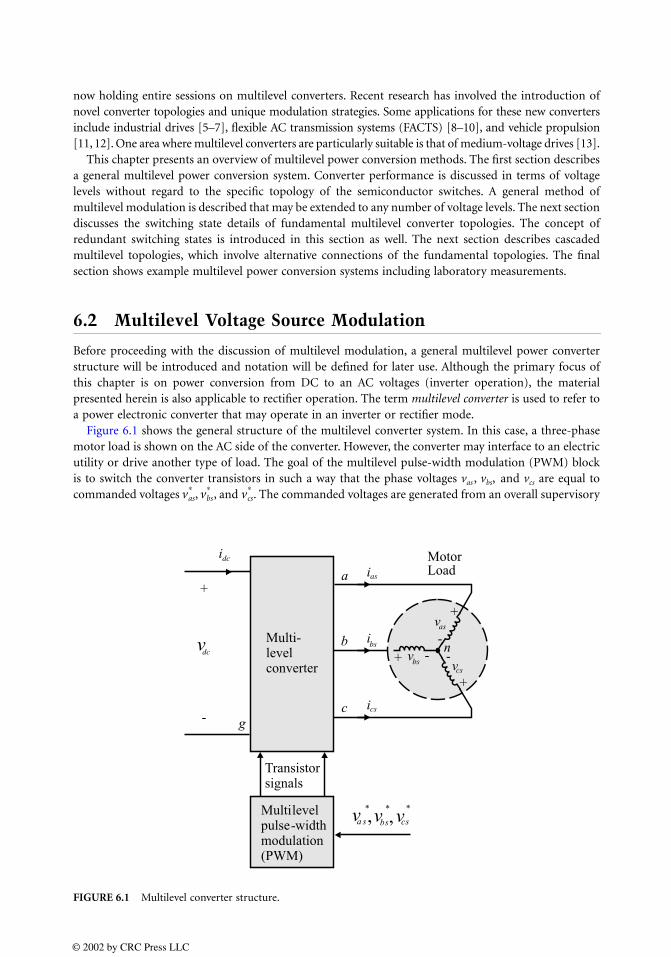
now holding entire sessions on multilevel converters. Recent research has involved the introduction ofnovel converter topologies and unique modulation strategies. Some applications for these new convertersinclude industrial drives [5–7], flexible AC transmission systems (FACTS) [8–10], and vehicle propulsion[11, 12]. One area where multilevel converters are particularly suitable is that of medium-voltage drives [13].
This chapter presents an overview of multilevel power conversion methods. The first section describesa general multilevel power conversion system. Converter performance is discussed in terms of voltagelevels without regard to the specific topology of the semiconductor switches. A general method ofmultilevel modulation is described that may be extended to any number of voltage levels. The next sectiondiscusses the switching state details of fundamental multilevel converter topologies. The concept ofredundant switching states is introduced in this section as well. The next section describes cascadedmultilevel topologies, which involve alternative connections of the fundamental topologies. The finalsection shows example multilevel power conversion systems including laboratory measurements.
6.2 Multilevel Voltage Source Modulation
Before proceeding with the discussion of multilevel modulation, a general multilevel power converterstructure will be introduced and notation will be defined for later use. Although the primary focus ofthis chapter is on power conversion from DC to an AC voltages (inverter operation), the materialpresented herein is also applicable to rectifier operation. The term multilevel converter is used to refer toa power electronic converter that may operate in an inverter or rectifier mode.
Figure 6.1 shows the general structure of the multilevel converter system. In this case, a three-phasemotor load is shown on the AC side of the converter. However, the converter may interface to an electricutility or drive another type of load. The goal of the multilevel pulse-width modulation (PWM) blockis to switch the converter transistors in such a way that the phase voltages vas , vbs, and vcs are equal tocommanded voltages , , and . The commanded voltages are generated from an overall supervisory
FIGURE 6.1 Multilevel converter structure.
vas∗ vbs
∗ vcs∗
dc
dc
as
as
bs
bs
cs
cs
© 2002 by CRC Press LLC
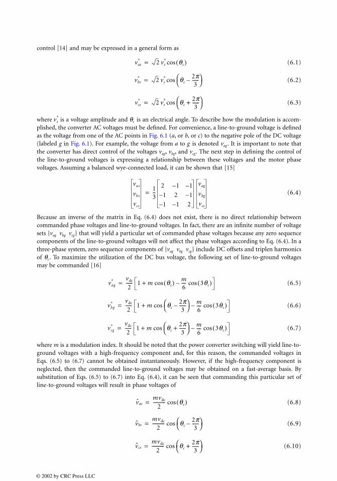
control [14] and may be expressed in a general form as
(6.1)
(6.2)
(6.3)
where is a voltage amplitude and θc is an electrical angle. To describe how the modulation is accom-plished, the converter AC voltages must be defined. For convenience, a line-to-ground voltage is definedas the voltage from one of the AC points in Fig. 6.1 (a, or b, or c) to the negative pole of the DC voltage(labeled g in Fig. 6.1). For example, the voltage from a to g is denoted vag . It is important to note thatthe converter has direct control of the voltages vag, vbg, and vcg. The next step in defining the control ofthe line-to-ground voltages is expressing a relationship between these voltages and the motor phasevoltages. Assuming a balanced wye-connected load, it can be shown that [15]
(6.4)
Because an inverse of the matrix in Eq. (6.4) does not exist, there is no direct relationship betweencommanded phase voltages and line-to-ground voltages. In fact, there are an infinite number of voltagesets vag vbg vcg that will yield a particular set of commanded phase voltages because any zero sequencecomponents of the line-to-ground voltages will not affect the phase voltages according to Eq. (6.4). In athree-phase system, zero sequence components of vag vbg vcg include DC offsets and triplen harmonicsof θc . To maximize the utilization of the DC bus voltage, the following set of line-to-ground voltagesmay be commanded [16]
(6.5)
(6.6)
(6.7)
where m is a modulation index. It should be noted that the power converter switching will yield line-to-ground voltages with a high-frequency component and, for this reason, the commanded voltages inEqs. (6.5) to (6.7) cannot be obtained instantaneously. However, if the high-frequency component isneglected, then the commanded line-to-ground voltages may be obtained on a fast-average basis. Bysubstitution of Eqs. (6.5) to (6.7) into Eq. (6.4), it can be seen that commanding this particular set ofline-to-ground voltages will result in phase voltages of
(6.8)
(6.9)
(6.10)
vas∗ 2 vs
∗ θc( )cos=
vbs∗ 2 vs
∗ θc2π3
------– cos=
vcs∗ 2 vs
∗ θc2π3
------+ cos=
vs∗
vas
vbs
vcs
13--
2 1– 1–
1– 2 1–
1– 1– 2
vag
vbg
vcs
=
vag∗ vdc
2------ 1 m θc( )cos
m6---- 3θc( )cos–+=
vbg∗ vdc
2------ 1 m θc
2π3
------– cos m
6---- 3θc( )cos–+=
vcg∗ vdc
2------ 1 m θc
2π3
------+ cos m
6---- 3θc( )cos–+=
vasmvdc
2----------- θc( )cos=
vbsmvdc
2----------- θc
2π3
------– cos=
vcsmvdc
2----------- θc
2π3
------+ cos=
© 2002 by CRC Press LLC

where the symbol denotes fast-average values. By comparing Eqs. (6.8) to (6.10) with Eqs. (6.1) to(6.3), it can be seen that the desired phase voltages are achieved if
(6.11)
It should be noted that in H-bridge-based converters, the range of line-to-ground voltage is twice thatof converters where one DC voltage supplies all three phases (as in Fig. 6.1). The modulation methodhere can accommodate these converters if the modulation index is related to the commanded voltagemagnitude by
(6.12)
The modulation process described here may be applied to H-bridge converters by substituting mH for min the equations that follow. The benefit of including the third harmonic terms in Eqs. (6.5) to (6.7) isan extended range of modulation index [16]. In particular, the range of the modulation index is
(6.13)
It is sometimes convenient to define a modulation index that has an upper limit of 100% or
(6.14)
The next step in the modulation process is to define normalized commanded line-to-ground voltages,which will be referred to as duty cycles. In terms of the modulation index and electrical angle, the dutycycles may be written:
(6.15)
(6.16)
(6.17)
To relate the duty cycles to the inverter switching operation, switching states must be defined that arevalid for any number of voltage levels. Here, the switching states for the a-, b-, and c-phase will be denotedsa, sb, and sc, respectively. Although the specific topology of the multilevel converter is covered in the nextsection, it may be stated in general for an n-level converter that the AC output consists of a number of
m2 2 vs
∗
vdc
----------------=
mH
2 vs∗
vdc
------------=
0 m2
3-------≤ ≤
m3
2------- m=
da12-- 1 m θc( )cos
m6---- 3θc( )cos–+=
db12-- 1 m θc
2π3
------– cos
m6---- 3θc( )cos–+=
dc12-- 1 m θc
2π3
------+ cos
m6---- 3θc( )cos–+=
© 2002 by CRC Press LLC
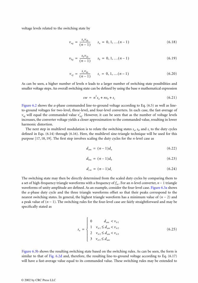
voltage levels related to the switching state by
(6.18)
(6.19)
(6.20)
As can be seen, a higher number of levels n leads to a larger number of switching state possibilities andsmaller voltage steps. An overall switching state can be defined by using the base n mathematical expression
(6.21)
Figure 6.2 shows the a-phase commanded line-to-ground voltage according to Eq. (6.5) as well as line-to-ground voltages for two-level, three-level, and four-level converters. In each case, the fast-average ofvag will equal the commanded value . However, it can be seen that as the number of voltage levelsincreases, the converter voltage yields a closer approximation to the commanded value, resulting in lowerharmonic distortion.
The next step in multilevel modulation is to relate the switching states sa, sb, and sc to the duty cyclesdefined in Eqs. (6.14) through (6.16). Here, the multilevel sine-triangle technique will be used for thispurpose [17, 18, 19]. The first step involves scaling the duty cycles for the n-level case as
(6.22)
(6.23)
(6.24)
The switching state may then be directly determined from the scaled duty cycles by comparing them toa set of high-frequency triangle waveforms with a frequency of fsw . For an n-level converter, n − 1 trianglewaveforms of unity amplitude are defined. As an example, consider the four-level case. Figure 6.3a showsthe a-phase duty cycle and the three triangle waveforms offset so that their peaks correspond to thenearest switching states. In general, the highest triangle waveform has a minimum value of (n − 2) anda peak value of (n − 1). The switching rules for the four-level case are fairly straightforward and may bespecifically stated as
(6.25)
Figure 6.3b shows the resulting switching state based on the switching rules. As can be seen, the form issimilar to that of Fig. 6.2d and, therefore, the resulting line-to-ground voltage according to Eq. (6.17)will have a fast-average value equal to its commanded value. These switching rules may be extended to
vag
savdc
n 1–( )---------------- sa 0, 1, … n 1–( )= =
vbg
sbvdc
n 1–( )---------------- sb 0, 1, … n 1–( )= =
vcg
scvdc
n 1–( )---------------- sc 0, 1, … n 1–( )= =
sw n2sa nsb sc+ +=
vag∗
dam n 1–( )da=
dbm n 1–( )db=
dcm n 1–( )dc=
sa
0 dam vtr1<1 vtr1 dam vtr2<≤2 vtr2 dam vtr3<≤3 vtr3 dam≤
=
© 2002 by CRC Press LLC
any number of levels by incorporating the appropriate number of triangle waveforms and definingswitching rules similar to Eq. (6.25). It should be pointed out that the sine-triangle method is shownhere since it is depicts a fairly straightforward method of accomplishing multilevel switching. In practice,the modulation is typically implemented on a digital signal processor (DSP) or erasable programmablelogic device (EPLD) without using triangle waveforms. One common method for implementation isspace-vector modulation [20–22], which is a method where the switching states are viewed in the voltagereference frame. Another method that may be used is duty-cycle modulation [23], which is a directcalculation method that uses duty cycles instead of triangle waveforms and is more readily implementableon a DSP. It is also possible to perform modulation based on a current-regulated approach [22, 24],which is fundamentally different than voltage-source modulation and results in a higher bandwidthcontrol of load currents.
FIGURE 6.2 Power converter line-to-ground output voltages.
ag
dc
ag
dc
ag
dc
ag
dc
© 2002 by CRC Press LLC
6.3 Fundamental Multilevel Converter Topologies
This section describes the most common multilevel converter topologies. In particular, the diode-clamped[25–28], flying capacitor [29, 30], cascaded H-bridge [31–33], and multilevel H-bridge [34] structuresare described. In each case, the process of creating voltage steps is illustrated and the relation to thegeneralized modulation scheme in the previous section is defined. For further study, the reader may beinterested in other topologies not discussed here, such as the parallel connected phase poles [35], ACmagnetically combined converters [36, 37], or soft-switching multilevel converters [38].
Diode-Clamped Multilevel Converters
One of the most common types of multilevel topologies is the diode-clamped multilevel converter[25–28]. Figure 6.4 shows the structure for the three-level case. Comparing this topology with that of astandard two-level converter, it can be seen that there are twice as many transistors as well as addeddiodes. However, it should be pointed out that the voltage rating of the transistors is half that of thetransistors in a two-level converter. Although the structure appears complex, the switching is fairlystraightforward. Figure 6.5 shows the a-phase leg of the three-level diode clamped converter along withthe corresponding switching states. Here, it is assumed that the transistors act as ideal switches and thatthe capacitor voltages are charged to half of the DC-link voltage. As can be seen in Fig. 6.5b, in switchingstate sa = 0, transistors Ta3 and Ta4 are gated on and the output voltage is vag = 0. Similarly, switching statesa = 2 involves gating on transistors Ta1 and Ta2 and the output voltage is vag = vdc. These switching statesproduce the same voltages as a two-level converter. Switching state sa = 1 involves gating on transistorsTa2 and Ta3 as shown in Fig. 6.5c. In this case, the point a is connected to the capacitor junction throughthe added diodes and the output voltage is vag = vdc/2. Note that for each of the switching states, the transistorblocking voltage is one half the DC-link voltage. When compared with the two-level converter, theadditional voltage level allows the production of line-to-ground voltages with lower harmonic distortion,as illustrated in Fig. 6.2. Furthermore, the switching losses for this converter will be lower than that ofa two-level converter. Switching losses are reduced by the lower transistor blocking voltage and increasedby the higher number of transistors. However, it can be seen by inspection of Figs. 6.2 and 6.5 that eachtransistor is switching only during a portion of the period of da, which again reduces the switchinglosses. Maintaining voltage balance on the capacitors can be accomplished through selection of the
FIGURE 6.3 Four-level sine-triangle modulation technique.
a
am
tr3
tr2
tr1
© 2002 by CRC Press LLC
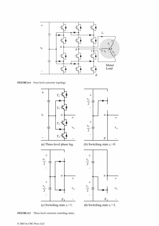
FIGURE 6.4 Four-level converter topology.
FIGURE 6.5 Three-level converter switching states.
as
as
cs bs
dc
a1
a2
a3
a4
agdc
dcdc
dc dc
dc
ag
ag ag
a
a
a
dc
© 2002 by CRC Press LLC
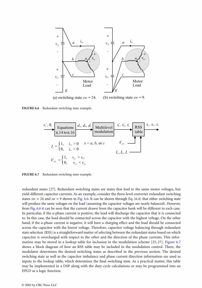
redundant states [27]. Redundant switching states are states that lead to the same motor voltages, butyield different capacitor currents. As an example, consider the three-level converter redundant switchingstates sw = 24 and sw = 9 shown in Fig. 6.6. It can be shown through Eq. (6.4) that either switching statewill produce the same voltages on the load (assuming the capacitor voltages are nearly balanced). However,from Fig. 6.6 it can be seen that the current drawn from the capacitor bank will be different in each case.In particular, if the a-phase current is positive, the load will discharge the capacitor that it is connectedto. In this case, the load should be connected across the capacitor with the highest voltage. On the otherhand, if the a-phase current is negative, it will have a charging effect and the load should be connectedacross the capacitor with the lowest voltage. Therefore, capacitor voltage balancing through redundantstate selection (RSS) is a straightforward matter of selecting between the redundant states based on whichcapacitor is overcharged with respect to the other and the direction of the phase currents. This infor-mation may be stored in a lookup table for inclusion in the modulation scheme [25, 27]. Figure 6.7shows a block diagram of how an RSS table may be included in the modulation control. There, themodulator determines the desired switching states as described in the previous section. The desiredswitching state as well as the capacitor imbalance and phase current direction information are used asinputs to the lookup table, which determines the final switching state. As a practical matter, this tablemay be implemented in a DSP along with the duty-cycle calculations or may be programmed into anEPLD as a logic function.
FIGURE 6.6 Redundant switching state example.
FIGURE 6.7 Redundant switching state example.
c2
asc2
as
c1 c1
as
as
s* * * *
c a
x
c12
c12
c1
c1
c2
c2
xs
xs
b c a b c a b c
a b c
© 2002 by CRC Press LLC
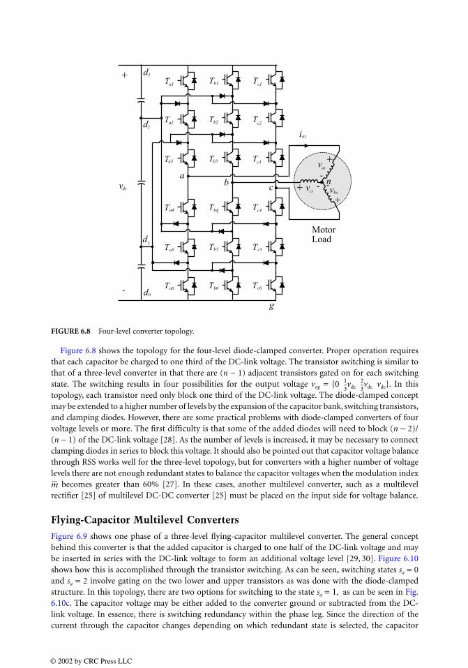
Figure 6.8 shows the topology for the four-level diode-clamped converter. Proper operation requiresthat each capacitor be charged to one third of the DC-link voltage. The transistor switching is similar tothat of a three-level converter in that there are (n − 1) adjacent transistors gated on for each switchingstate. The switching results in four possibilities for the output voltage vag = 0 vdc vdc vdc. In thistopology, each transistor need only block one third of the DC-link voltage. The diode-clamped conceptmay be extended to a higher number of levels by the expansion of the capacitor bank, switching transistors,and clamping diodes. However, there are some practical problems with diode-clamped converters of fourvoltage levels or more. The first difficulty is that some of the added diodes will need to block (n − 2)/(n − 1) of the DC-link voltage [28]. As the number of levels is increased, it may be necessary to connectclamping diodes in series to block this voltage. It should also be pointed out that capacitor voltage balancethrough RSS works well for the three-level topology, but for converters with a higher number of voltagelevels there are not enough redundant states to balance the capacitor voltages when the modulation index
becomes greater than 60% [27]. In these cases, another multilevel converter, such as a multilevelrectifier [25] of multilevel DC-DC converter [25] must be placed on the input side for voltage balance.
Flying-Capacitor Multilevel Converters
Figure 6.9 shows one phase of a three-level flying-capacitor multilevel converter. The general conceptbehind this converter is that the added capacitor is charged to one half of the DC-link voltage and maybe inserted in series with the DC-link voltage to form an additional voltage level [29, 30]. Figure 6.10shows how this is accomplished through the transistor switching. As can be seen, switching states sa = 0and sa = 2 involve gating on the two lower and upper transistors as was done with the diode-clampedstructure. In this topology, there are two options for switching to the state sa = 1, as can be seen in Fig.6.10c. The capacitor voltage may be either added to the converter ground or subtracted from the DC-link voltage. In essence, there is switching redundancy within the phase leg. Since the direction of thecurrent through the capacitor changes depending on which redundant state is selected, the capacitor
FIGURE 6.8 Four-level converter topology.
3
a1 b1
a2 b2
a3 b3
c1
as
as
cs bs
c2
c3
a4
a5
a6
0
b6 c6
b4 c4
c5b51
dc
2
13-- 2
3--
m
© 2002 by CRC Press LLC

voltage may be maintained at one half the DC-link voltage through the redundant state selection withinthe phase.
Cascaded H-Bridge Multilevel Converters
Cascaded H-bridge converters consist of a number of H-bridge power conversion cells, each supplied byan isolated source on the DC side and series-connected on the AC side [31–33]. Figure 6.11 shows thea-phase of a cascaded H-bridge converter, where two H-bridge cells are utilized. It should be pointedout that, unlike the diode-clamped and flying-capacitor topologies, isolated sources are required for eachcell in each phase. In some systems these sources may be available through batteries or photovoltaic cells[32], but in most drive systems transformer/rectifier sources are used. Figure 6.12 illustrates the switchingstate detail for one H-bridge cell. As can be seen, three unique output voltages are possible. In accordancewith the convention used here, the lowest switching state will be labeled state 0. When these cells arecombined in series, an effective switching state can be related to the switching states of the individualcells. By defining switching states in this way, the modulation scheme of the previous section may beapplied to this converter as well. The output voltage of the inverter may be determined from the switchingstates of the individual cells by
(6.26)
where p is the number of series H-bridge cells.If the DC voltage applied to each cell is set to the same value, then the effective number of voltage
levels may be related to the number of cells by
(6.27)
Therefore, the converter shown in Fig. 6.10 would operate with five voltage levels. To obtain a clearercomprehension of how the voltage levels are produced, Table 6.1 shows the overall switching state as wellas the switching states of the individual cells and the resulting output voltage. As can be seen, there isquite a bit of switching state redundancy within one phase leg of the cascaded H-bridge converter forstates sa = 1, sa = 2, and sa = 3. This redundancy may be exploited to increase the number of voltage levels
FIGURE 6.9 Three-level flyback converter topology.
a1
a2
a3
a4
ag
dc
vag Sai 1–( )vdc i
i=0
p
∑=
n 3 2 p 1–( )+=
© 2002 by CRC Press LLC
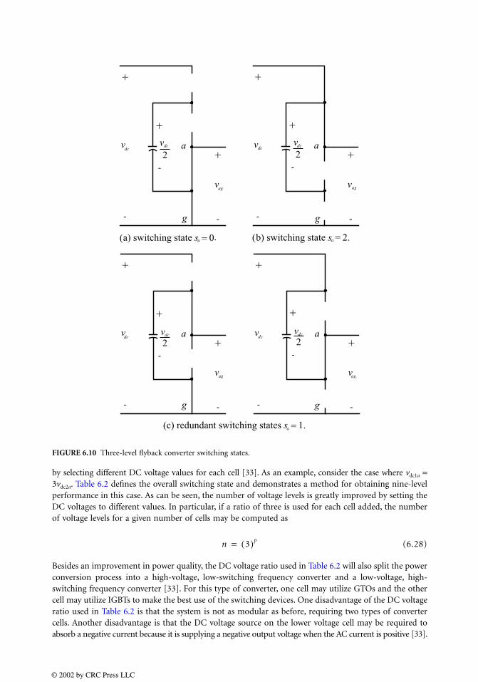
by selecting different DC voltage values for each cell [33]. As an example, consider the case where vdc1a =3vdc2a. Table 6.2 defines the overall switching state and demonstrates a method for obtaining nine-levelperformance in this case. As can be seen, the number of voltage levels is greatly improved by setting theDC voltages to different values. In particular, if a ratio of three is used for each cell added, the numberof voltage levels for a given number of cells may be computed as
(6.28)
Besides an improvement in power quality, the DC voltage ratio used in Table 6.2 will also split the powerconversion process into a high-voltage, low-switching frequency converter and a low-voltage, high-switching frequency converter [33]. For this type of converter, one cell may utilize GTOs and the othercell may utilize IGBTs to make the best use of the switching devices. One disadvantage of the DC voltageratio used in Table 6.2 is that the system is not as modular as before, requiring two types of convertercells. Another disadvantage is that the DC voltage source on the lower voltage cell may be required toabsorb a negative current because it is supplying a negative output voltage when the AC current is positive [33].
FIGURE 6.10 Three-level flyback converter switching states.
dcdc dc dc
ag
a a
ag
dcdcdcdc
agag
a
n 3( )p=
© 2002 by CRC Press LLC
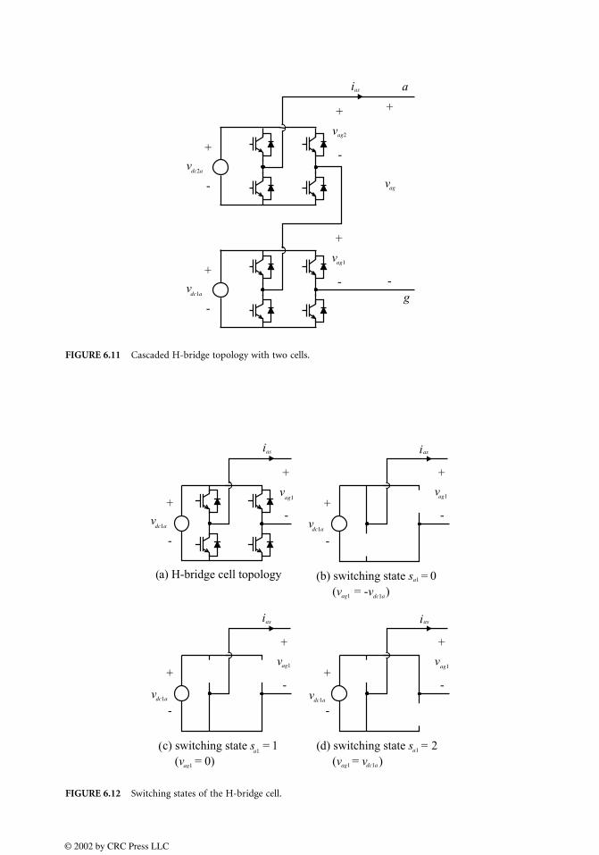
FIGURE 6.11 Cascaded H-bridge topology with two cells.
FIGURE 6.12 Switching states of the H-bridge cell.
dc2a
dc1a
ag1
ag2
ag
as
dc1a
dc1a
dc1a
dc1a dc1a
dc1a
ag1ag1
ag1
ag1ag1
ag1
a1
a1
a1
ag1
asas
as as
© 2002 by CRC Press LLC
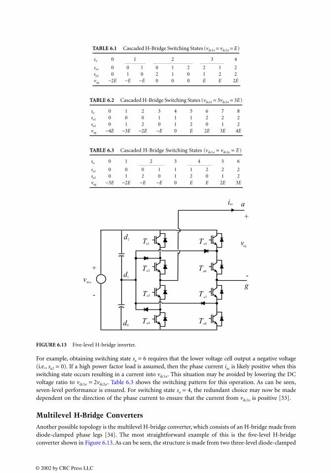
For example, obtaining switching state sa = 6 requires that the lower voltage cell output a negative voltage(i.e., sa2 = 0). If a high power factor load is assumed, then the phase current ias is likely positive when thisswitching state occurs resulting in a current into vdc1a. This situation may be avoided by lowering the DCvoltage ratio to vdc1a = 2vdc2a . Table 6.3 shows the switching pattern for this operation. As can be seen,seven-level performance is ensured. For switching state sa = 4, the redundant choice may now be madedependent on the direction of the phase current to ensure that the current from vdc2a is positive [33].
Multilevel H-Bridge Converters
Another possible topology is the multilevel H-bridge converter, which consists of an H-bridge made fromdiode-clamped phase legs [34]. The most straightforward example of this is the five-level H-bridgeconverter shown in Figure 6.13. As can be seen, the structure is made from two three-level diode-clamped
TABLE 6.1 Cascaded H-Bridge Switching States (vdc1a = vdc2a = E)
sa 0 1 2 3 4
sa1 0 0 1 0 1 2 2 1 2 sa2 0 1 0 2 1 0 1 2 2 vag −2E −E −E 0 0 0 E E 2E
TABLE 6.2 Cascaded H-Bridge Switching States (vdca1 = 3vdc2a = 3E)
sa 0 1 2 3 4 5 6 7 8 sa1 0 0 0 1 1 1 2 2 2 sa2 0 1 2 0 1 2 0 1 2 vag −4E −3E −2E −E 0 E 2E 3E 4E
TABLE 6.3 Cascaded H-Bridge Switching States (vdc1a = vdc2a = E)
sa 0 1 2 3 4 5 6
sa1 0 0 0 1 1 1 2 2 2 sa2 0 1 2 0 1 2 0 1 2 vag −3E −2E −E −E 0 E E 2E 3E
FIGURE 6.13 Five-level H-bridge inverter.
ag
dca
a1
a2
2
1
0
a3
a4 a8
a7
a6
a5
as
© 2002 by CRC Press LLC
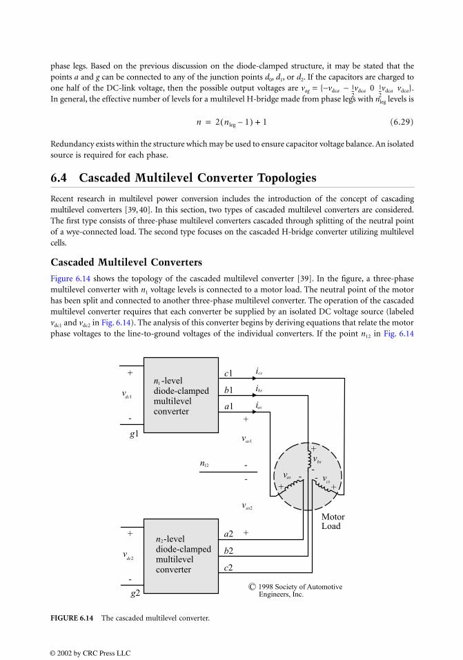
phase legs. Based on the previous discussion on the diode-clamped structure, it may be stated that thepoints a and g can be connected to any of the junction points d0, d1, or d2. If the capacitors are charged toone half of the DC-link voltage, then the possible output voltages are vag = −vdca − vdca 0 vdca vdca.In general, the effective number of levels for a multilevel H-bridge made from phase legs with nleg levels is
(6.29)
Redundancy exists within the structure which may be used to ensure capacitor voltage balance. An isolatedsource is required for each phase.
6.4 Cascaded Multilevel Converter Topologies
Recent research in multilevel power conversion includes the introduction of the concept of cascadingmultilevel converters [39, 40]. In this section, two types of cascaded multilevel converters are considered.The first type consists of three-phase multilevel converters cascaded through splitting of the neutral pointof a wye-connected load. The second type focuses on the cascaded H-bridge converter utilizing multilevelcells.
Cascaded Multilevel Converters
Figure 6.14 shows the topology of the cascaded multilevel converter [39]. In the figure, a three-phasemultilevel converter with n1 voltage levels is connected to a motor load. The neutral point of the motorhas been split and connected to another three-phase multilevel converter. The operation of the cascadedmultilevel converter requires that each converter be supplied by an isolated DC voltage source (labeledvdc1 and vdc2 in Fig. 6.14). The analysis of this converter begins by deriving equations that relate the motorphase voltages to the line-to-ground voltages of the individual converters. If the point n12 in Fig. 6.14
FIGURE 6.14 The cascaded multilevel converter.
12-- 1
2--
n 2 nleg 1–( ) 1+=
dc1
1
2
12
dc2
as1
as2
as
as
bs
bs
cs
cs
© 2002 by CRC Press LLC

indicates a fictitious neutral point, then the phase voltages from converter 1 may be written similar toEq. (6.4). In particular [39]
(6.30)
where the line-to-ground voltages are defined with respect to the negative DC rail of vdc1. For exampleva1g1 is the voltage from the point a1 to g1. Similarly for converter 2,
(6.31)
By applying KVL equations to the circuit topology, it can be seen that
(6.32)
(6.33)
(6.34)
Substitution of Eqs. (6.30) and (6.31) into Eqs. (6.32) to (6.34) yields
(6.35)
By comparison of Eq. (6.35) to Eq. (6.4), it can be seen that the effective line-to-ground voltage is thedifference of the line-to-ground voltages from converter 1 to converter 2. The effective number of voltage levelsin this cascaded topology depends on the ratio of the DC voltages. It has been shown that the maxi-mum number of voltage levels achievable is the product of the voltage levels of the individual convertersor [39]
(6.36)
To obtain this number of effective voltage levels, the DC voltage ratio must be set to [39]
(6.37)
As with the cascaded H-bridge inverter described in Section 6.3, the switching states of each convertermay be related to an overall switching state in order to utilize the same multilevel modulation techniqueof Section 6.2. A specific example of this is given in the following section where a three-level diode-clamped converter is cascaded with a two-level converter to form an effective six-level converter.
Cascaded Multilevel H-Bridge Converters
Combining the concept of cascading converters with the cascaded H-bridge converter described inSection 6.3, it stands to reason that a cascaded H-bridge converter can be made from multilevel H-bridgecells. The general concept is shown in Fig. 6.15, which depicts the a-phase of a cascaded H-bridge
vas1
vbs1
vcs1
13--
2 1– 1–
1– 2 1–
1– 1– 2
va1g1
vb1g1
vc1g1
=
vas2
vbs2
vcs2
13--
2 1– 1–
1– 2 1–
1– 1– 2
va2g2
vb2g2
vc2g2
=
vas vas1 vas2–=
vbs vbs1 vbs2–=
vcs vcs1 vcs2–=
vas
vbs
vcs
13--
2 1– 1–
1– 2 1–
1– 1– 2
va1g1 va2g2–
vb1g1 vb2g2–
vc1g1 vc2g2–
=
n n1n2=
vdc2
vdc1
--------n2 1–
n2 n1 1–( )------------------------=
© 2002 by CRC Press LLC
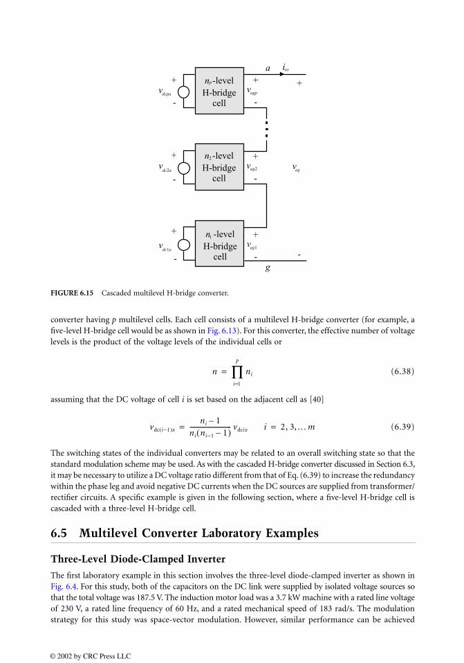
converter having p multilevel cells. Each cell consists of a multilevel H-bridge converter (for example, afive-level H-bridge cell would be as shown in Fig. 6.13). For this converter, the effective number of voltagelevels is the product of the voltage levels of the individual cells or
(6.38)
assuming that the DC voltage of cell i is set based on the adjacent cell as [40]
(6.39)
The switching states of the individual converters may be related to an overall switching state so that thestandard modulation scheme may be used. As with the cascaded H-bridge converter discussed in Section 6.3,it may be necessary to utilize a DC voltage ratio different from that of Eq. (6.39) to increase the redundancywithin the phase leg and avoid negative DC currents when the DC sources are supplied from transformer/rectifier circuits. A specific example is given in the following section, where a five-level H-bridge cell iscascaded with a three-level H-bridge cell.
6.5 Multilevel Converter Laboratory Examples
Three-Level Diode-Clamped Inverter
The first laboratory example in this section involves the three-level diode-clamped inverter as shown inFig. 6.4. For this study, both of the capacitors on the DC link were supplied by isolated voltage sources sothat the total voltage was 187.5 V. The induction motor load was a 3.7 kW machine with a rated line voltageof 230 V, a rated line frequency of 60 Hz, and a rated mechanical speed of 183 rad/s. The modulationstrategy for this study was space-vector modulation. However, similar performance can be achieved
FIGURE 6.15 Cascaded multilevel H-bridge converter.
dcpa
dc2a
dc1a
ag
ag1
ag2
as
agp
1
2
p
n ni
i=1
p
∏=
vdc i−1( )xni 1–
ni ni−1 1–( )--------------------------- vdcix i 2, 3,… m= =
© 2002 by CRC Press LLC
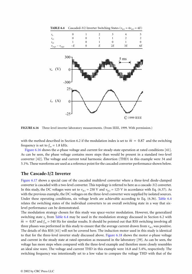
with the method described in Section 6.2 if the modulation index is set to and the switchingfrequency is set to fsw = 1.8 kHz.
Figure 6.16 shows the a-phase voltage and current for steady-state operation at rated conditions [41].As can be seen, the phase voltage contains more steps than would be present in a standard two-levelconverter [42]. The voltage and current total harmonic distortion (THD) in this example were 34 and5.1%. These waveforms are used as a reference point for the cascaded converter performance shown below.
The Cascade-3/2 Inverter
Figure 6.17 shows a special case of the cascaded multilevel converter where a three-level diode-clampedconverter is cascaded with a two-level converter. This topology is referred to here as a cascade-3/2 converter.In this study, the DC voltages were set to vdc1 = 250 V and vdc2 = 125 V in accordance with Eq. (6.37). Aswith the previous example, the DC voltages on the three-level converter were supplied by isolated sources.Under these operating conditions, six voltage levels are achievable according to Eq. (6.36). Table 6.4relates the switching states of the individual converters to an overall switching state in a way that six-level performance can be demonstrated. The modulation strategy chosen for this study was space-vector modulation. However, the generalizedswitching state sa from Table 6.4 may be used in the modulation strategy discussed in Section 6.2 with
and fsw = 540 Hz for similar results. It should be pointed out that RSS switching involving allthree phases was performed in this study to ensure that the average current drawn from vdc2 was positive.The details of this RSS [41] will not be covered here. The induction motor used in this study is identicalto that for the three-level inverter study discussed above. Figure 6.18 shows the motor a-phase voltageand current in the steady state at rated operation as measured in the laboratory [39]. As can be seen, thevoltage has more steps when compared with the three-level example and therefore more closely resemblesan ideal sine wave. The voltage and current THD in this example were 16.8 and 5.4%, respectively. Theswitching frequency was intentionally set to a low value to compare the voltage THD with that of the
TABLE 6.4 Cascaded-3/2 Inverter Switching States (vdc1 = 4vdc2 = 4E)
sa 0 1 2 3 4 5 sa1 0 0 1 1 2 2 sa2 1 0 1 0 1 0 va1g1 − va2g2 −E 0 E 2E 3E 4E
FIGURE 6.16 Three-level inverter laboratory measurements. (From IEEE, 1999. With permission.)
as
as
m 0.87=
m 0.87=
© 2002 by CRC Press LLC
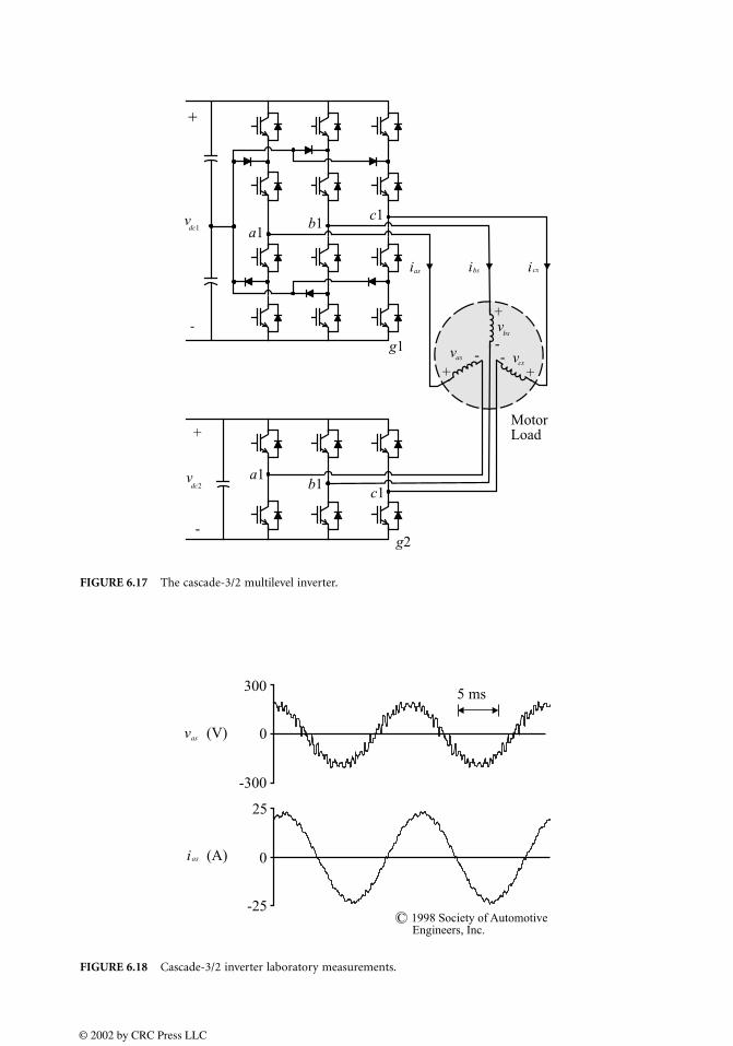
FIGURE 6.17 The cascade-3/2 multilevel inverter.
FIGURE 6.18 Cascade-3/2 inverter laboratory measurements.
dc1
dc2
as
as
bs
bs
cs
cs
as
as
© 2002 by CRC Press LLC
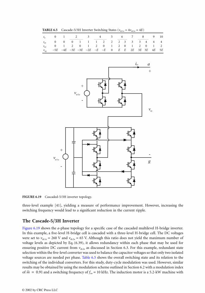
three-level example [41], yielding a measure of performance improvement. However, increasing theswitching frequency would lead to a significant reduction in the current ripple.
The Cascade-5/3H Inverter
Figure 6.19 shows the a-phase topology for a specific case of the cascaded multilevel H-bridge inverter.In this example, a five-level H-bridge cell is cascaded with a three-level H-bridge cell. The DC voltageswere set to vdc1a = 260 V and vdc2a = 65 V. Although this ratio does not yield the maximum number ofvoltage levels as depicted by Eq. (6.39), it allows redundancy within each phase that may be used forensuring positive DC current from vdc2a as discussed in Section 6.3. For this example, redundant stateselection within the five-level converter was used to balance the capacitor voltages so that only two isolatedvoltage sources are needed per phase. Table 6.5 shows the overall switching state and its relation to theswitching of the individual converters. For this study, duty-cycle modulation was used. However, similarresults may be obtained by using the modulation scheme outlined in Section 6.2 with a modulation indexof and a switching frequency of fsw = 10 kHz. The induction motor is a 5.2-kW machine with
TABLE 6.5 Cascade-5/3H Inverter Switching States (vdc1a = 4vdc2a = 4E)
sa 0 1 2 3 4 5 6 7 8 9 10
sa1 0 0 0 1 1 1 2 2 2 3 3 3 4 4 4 sa2 0 1 2 0 1 2 0 1 2 0 1 2 0 1 2 vag −5E −4E −3E −3E −2E −E −E 0 E E 2E 3E 3E 4E 5E
FIGURE 6.19 Cascaded-5/3H inverter topology.
dc2a
dc1a
ag
as
m 0.91=
© 2002 by CRC Press LLC

a rated line voltage of 460 V. Figure 6.20 shows the measured performance of the inverter operating atrated voltage and a power level of 3.7 kW. Therein, the a-phase voltage, current, and capacitor voltagesare shown. As can be seen, from the motor voltage, the number of steps is greatly increased from thethree- and six-level inverter examples shown above. The voltage and current THD in this example are 6.5and 3.7%, respectively. It can also be seen from the capacitor voltages that the RSS algorithm is effective.
6.6 Conclusion
This chapter has presented an overview of multilevel power conversion. Multilevel voltage-source modula-tion was introduced and formulated in terms of a per-phase switching state which related to the converterline-to-ground voltage. Several topologies for performing multilevel power conversion were presented andthe switching states were defined to match that of the modulation. In this way, the generalized multilevelmodulation technique can be readily applied to any of the specific topologies. Two types of cascadedmultilevel topologies were discussed. The advantage of cascading multilevel converters is the large numberof voltage levels available as the result of a compounding effect of cascading process. A few laboratoryexamples were given that demonstrated the performance achievable through multilevel power converters.
FIGURE 6.20 Cascade-5/3H inverter laboratory measurements.
c1
c2
as
as (V)
© 2002 by CRC Press LLC

References
1. Nabe, A., Takahashi, I., and Akagi, H., A new neutral-point clamped PWM inverter, IEEE Trans. Ind.Appl., 17, 518, 1981.
2. Corzine, K. A. and Majeethia, S. K., Analysis of a novel four-level DC/DC boost converter, IEEETrans. Ind. Appl., 36, 1342, 2000.
3. Tolbert, L. M. and Peng, F. Z., Multilevel converters for large electric drives, IEEE Trans. Ind. Appl.,35, 36, 1999.
4. Rojas, R., Ohnishi, T., and Suzuki, T., PWM control method for a four-level inverter, in Proc. ElectricPower Applications, IEE, 1995, 390.
5. Tenconi, S. M., Carpita, M., Bacigalupo, C., and Cali, R., Multilevel voltage source converter formedium voltage adjustable speed drives, in Proc. ISIE, IEEE, Athens, 1995, 91.
6. Osman, R. H., A medium-voltage drive utilizing series-cell multilevel topology for outstanding powerquality, in Proc. IAS, IEEE, Phoenix, 1999, 2662.
7. Mahfouz, A., Holtz, J., and El-Tobshy, A., Development of an integrated high-voltage 3-level converter-inverter system with sinusoidal input-output for feeding 3-phase induction motors, in Proc. 5thEuropean Conference on Power Electronics and Applications, Brighton, U.K., 1993, 134.
8. Seki, N. and Uchino, H., Converter configurations and switching frequency for a GTO reactive powercompensator, IEEE Trans. Ind. Appl., 33, 1011, 1997.
9. Chen, Y., Mwinyiwiwa, B., Wolanski, Z., and Ooi, B. T., Regulating and equalizing DC capacitivevoltages in multilevel statcom, IEEE Trans. Power Delivery, 12, 901, 1997.
10. Hatziadoniu, C. J. and Chalkiadakis, F. E., A 12-pulse static synchronous compensator for thedistribution system employing the 3-level GTO-inverter, IEEE Trans. Power Delivery, 12, 1830, 1997.
11. Nakata, K., Nakamura, K., and Ito, S., A three-level traction inverter with IGBTS for EMU, in Proc.IAS, IEEE, Denver, 1994, 667.
12. Willkinson, R. H., Horn, A., and Enslin, J. H. R., Control options for a bi-directional multileveltraction chopper, in Proc. PESC, IEEE, Maggiore, 1996, 1395.
13. Lyons, J. P., Vlatkovic, V., Espelage, P. M., Boettner, F. H., and Larsen, E., Innovation IGCT maindrives, in Proc. IAS, IEEE, Phoenix, 1999, 2655.
14. Vas, P., Sensorless Vector and Direct Torque Control, Oxford University Press, Oxford, 1998, chap. 2.15. Krause, P. C., Wasynczuk, O., and Sudhoff, S. D., Analysis of Electric Machinery, IEEE Press, Piscat-
away, NJ, 1995, chap. 13.16. Houldsworth, J. A. and Grant, D. A., The use of harmonic distortion to increase the output voltage
of a three-phase pwm inverter, IEEE Trans. Ind. Appl., 20, 1224, 1984.17. Corzine, K. A., Sudhoff, S. D., Lewis, E. A., Schmucker, D. H., Youngs, R. A., and Hegner, H. J., Use
of multi-level converters in ship propulsion drives, in Proc. All Electric Ship Conference, IMarE,London, 1998, 155.
18. Tolbert, L. M. and Peng, F. Z., Multilevel PWM methods at low modulation indices, IEEE Trans.Power Electron., 15, 719, 2000.
19. Menzies, R. W., Steimer, P., and Steknke, J. K., Five-level GTO inverter for large induction motordrives, IEEE Trans. Ind. Appl., 30, 1994.
20. Liu, H. L. and Cho, G. H., Three-level space vector PWM in low index modulation region avoidingnarrow pulse problem, IEEE Trans. Power Electron., 9, 481, 1994.
21. Lee, Y. H., Suh, B. S., and Hyun, D. S., A novel PWM scheme for a three-level voltage source inverterwith GTO thyristors, IEEE Trans. Ind. Appl., 32, 260, 1996.
22. Corzine, K. A., A hysteresis current-regulated control for multi-level converters, IEEE Trans. EnergyConversion, 15, 169, 2000.
23. Corzine, K. A. and Majeethia, S. K., Analysis of a novel four-level DC/DC boost converter, in Proc.IAS, IEEE, Phoenix, 1999, 1964.
24. Marchesoni, M., High-performance current control techniques for applications to multilevel high-power voltage source inverters, IEEE Trans. Power Electron., 7, 189, 1992.
© 2002 by CRC Press LLC

25. Corzine, K. A., Delisle, D. E., Borraccini, J. P., and Baker, J. R., Multi-level power conversion:present research and future investigations, in Proc. All Electric Ship Conference, IMarE, Paris,France, 2000.
26. Corzine, K. A., Topology and Control of Cascaded Multi-Level Converters, Ph.D. dissertation,University of Missouri, Rolla, 1997.
27. Fracchia, M., Ghiara, T., Marchesoni, M., and Mazzucchelli, M., Optimized modulation techniquesfor the generalized n-level converter, in Proc. PESC, IEEE, Madrid, 1992, 1205.
28. Horn, A., Wilkinson, R. H., and Enslin, J. H. R., Evaluation of converter topologies for improvedpower quality in DC traction, in Proc. ISIE, IEEE, Warsaw, 1996, 802.
29. Tourkhani, F., Viarouge, P., and Meynard, T. A., A simulation-optimization system for the optimaldesign of a multilevel inverter, IEEE Trans. Power Electron., 14, 1037, 1999.
30. Yuan, X. and Barbi, I., Zero-voltage switching for three-level capacitor clamping inverter, IEEE Trans.Power Electron., 14, 771, 1999.
31. Hammond, P. W., Medium Voltage PWM Drive and Method, U.S. Patent 5,625,545, 1997.32. Calais, M., Agelidis, V. G., Borle, L. J., and Dymond, M. S., A transformerless five level cascaded
inverter based single phase photovoltaic system, in Proc. PESC, IEEE, Galway, 2000, 1173.33. Lipo, T. A. and Menjrekar, M. D., Hybrid Topology for Multi-Level Power Conversion, U.S. Patent
6,005,788, 1999.34. Hill, W. A. and Harbourt, C. D., Performance of medium voltage multi-level inverters, in Proc. IAS,
IEEE, Phoenix, 1999, 1186.35. Matsui, K., Asao, M., Ueda, F., Tsuboi, K., and Iwata, K., A technique of parallel-connections of
pulsewidth modulated NPC inverters by using current sharing reactors, in Proc. IECON, IEEE, Maui,1993, 1246.
36. Iturriz, F. and Ladoux, P., Phase-controlled multilevel converters based on dual structure associations,IEEE Trans. Power Electron., 15, 92, 2000.
37. Masukawa, S. and Iida, S., A method of reducing harmonics in output voltages of a double-connectedinverter, IEEE Trans. Power Electron., 9, 543.
38. Yamamoto, M., Hiraki, E., Iwamoto, H. Sugimoto, S., Kouda, I., and Nakaoka, M., Voltage-fed NPCsoft-switched inverter with new space voltage vector modulation scheme, in Proc. IAS, IEEE, Phoenix,1999, 1178.
39. Corzine, K. A. and Sudhoff, S. D., High state count power converters: an alternate direction in powerelectronics technology, SAE Trans. J. Aerospace, SAE paper number 981266 © 1998 Society of Auto-motive Engineers, Inc., Williamsburg, 1, 124, 1998.
40. Corzine, K. A., Use of multi-level inverters to reduce high-frequency effects in induction motordrives, in Proc. Naval Symposium on Electric Machines, ONR/NSWC, Philadelphia, 2000.
41. Corzine, K. A., Sudhoff, S. D., and Whitcomb, C. A., Performance characteristics of a cascaded two-level converter, IEEE Trans. Energy Conversion, 14, 433, 1999.
42. Hart, D. W., Introduction to Power Electronics, Prentice-Hall, Upper Saddle River, NJ, 1997, chap. 8.
© 2002 by CRC Press LLC

7Modulation Strategies
7.1 Introduction7.2 Six-Step Modulation7.3 Pulse Width Modulation
PWM Signals with DC Average • PWM Signals for AC Output
7.4 Third Harmonic Injection for Voltage Boost of SPWM Signals
7.5 Generation of PWM Signals Using Microcontrollersand DSPs
7.6 Voltage Source–Based Current Regulation7.7 Hysteresis Feedback Control
Introduction • Principles of the Hysteresis Feedback Control Circuits • Design Procedure • Experimental Results • Conclusions
7.8 Space-Vector Pulse Width ModulationHow the SVPWM Works • Implementation • Switching Signals
7.1 Introduction
Michael Giesselmann
In this chapter, modulation techniques for power electronics circuits are discussed. Modulation tech-niques are strategies to control the state of switches in these circuits. Switch mode is preferred to linearoperation since switches ideally do not dissipate any power in either the ON or OFF state. Dependingon the switches that are being used, it may only be possible to control the turn on instants. However,most modern power semiconductors such as IGBTs can be turned on and off tens of thousands of timesper second on command. In parallel with the development of these modern power semiconductors, newmodulation techniques have emerged. In the following sections, a number of modulation techniquesalong with their advantages and disadvantages will be discussed. Most figures have been generated usingMathCAD® 2000 [1]. The examples for the digital modulation techniques and the voltage source–basedcurrent control techniques have been generated using PSpice®[2].
References
1. MathCAD® 2000 Professional, MathSoft Engineering & Education, Inc., 101 Main Street, Cambridge,MA 02142-1521, http://www.mathsoft.com.
2. PSpice® Documentation, 555 River Oaks Parkway, San Jose, CA 95134, U.S.A.; (408)-943-1234;http://pcb.cadence.com/.
Michael Giesselmann Texas Tech University
Hossein SalehfarUniversity of North Dakota
Hamid A. ToliyatTexas A&M University
Tahmid Ur RahmanTexas A&M University
© 2002 by CRC Press LLC

7.2 Six-Step Modulation
Michael Giesselmann
Six-step modulation represents an early technique to control a three-phase inverter. Six-step modulationuses a sequence of six switching patterns for the three phase legs of a full-bridge inverter to generate afull cycle of three-phase voltages. A switch pair connected between the positive DC bus and the negativeDC bus represents a phase leg. The output terminal is the midpoint of the two switches. Only one switchof a phase leg may be turned on at any given time to prevent a short circuit between the DC buses. Onestate of the inverter leg represents the case when the upper switch is turned on whereas the opposite stateis represented by the lower switch being turned on. If each phase leg has these two states, the inverter has2
3 = 8 possible switching states. Six of these states are active states, whereas the two states in which either
all of the upper or all of the lower switches are turned on are called zero states, because the line-to-lineoutput voltage is zero in these cases. The six discrete switching patterns for six-step modulation are shownin Fig. 7.1a to f. For clarity, free-wheeling diodes have been omitted. After the switching pattern shownin Fig. 7.1f, the cycle begins anew with the switching pattern shown in Fig. 7.1a. Note that in subsequentpatterns, only a single inverter leg changes states. The switching patterns shown in Fig. 7.1a to f representthe following inverter states in the following order:
• Positive peak of Phase A
• Negative peak of Phase C
• Positive peak of Phase B
• Negative peak of Phase A
• Positive peak of Phase C
• Negative peak of Phase B
The aforementioned inverter states are equally spaced in a circle with 60° of phase shift between them.This is illustrated in Fig. 7.2. The hexagon in Fig. 7.2 represents the trace of a voltage vector around acircle for six-step modulation. This scheme could be extended to space vector modulation, if the voltagevector would not make discrete 60° steps, but would alternate at high speed between two adjacent states.The switching control would be such that the average time spend in the previous state is graduallydecreasing, whereas the average time spent in the next state is gradually increasing. Also by inserting zerostates, the magnitude of the output voltage could be controlled.
Figure 7.3 shows the phase to neutral waveform of one inverter leg for six-step operation if the neutral pointis considered the midpoint between the positive and negative bus. The resulting line-to-line output voltageis shown in Fig. 7.4. This waveform is closer to a sinusoid than the phase to neutral voltage but it still has aconsiderable amount of harmonics. Figure 7.5 shows the spectrum of the line-to-line voltage for six-stepoperation normalized to the fundamental frequency. The lowest harmonic component is the 5th harmonic.
The advantages of six-step modulation are the simplicity of the procedure and the ability to use slow-switching, high-power devices like GTOs. However, the harmonic content of the output voltage and theinability to control the magnitude of the output voltage are serious drawbacks. Because of these drawbacksand due to the recent advances in high-power IGBT technology, this modulation scheme is today seldomconsidered for new designs.
7.3 Pulse Width Modulation
Michael Giesselmann
Pulse width modulation (PWM) is the method of choice to control modern power electronics circuits. Thebasic idea is to control the duty cycle of a switch such that a load sees a controllable average voltage. Toachieve this, the switching frequency (repetition frequency for the PWM signal) is chosen high enoughthat the load cannot follow the individual switching events. Switching, rather than linear operation of the
© 2002 by CRC Press LLC
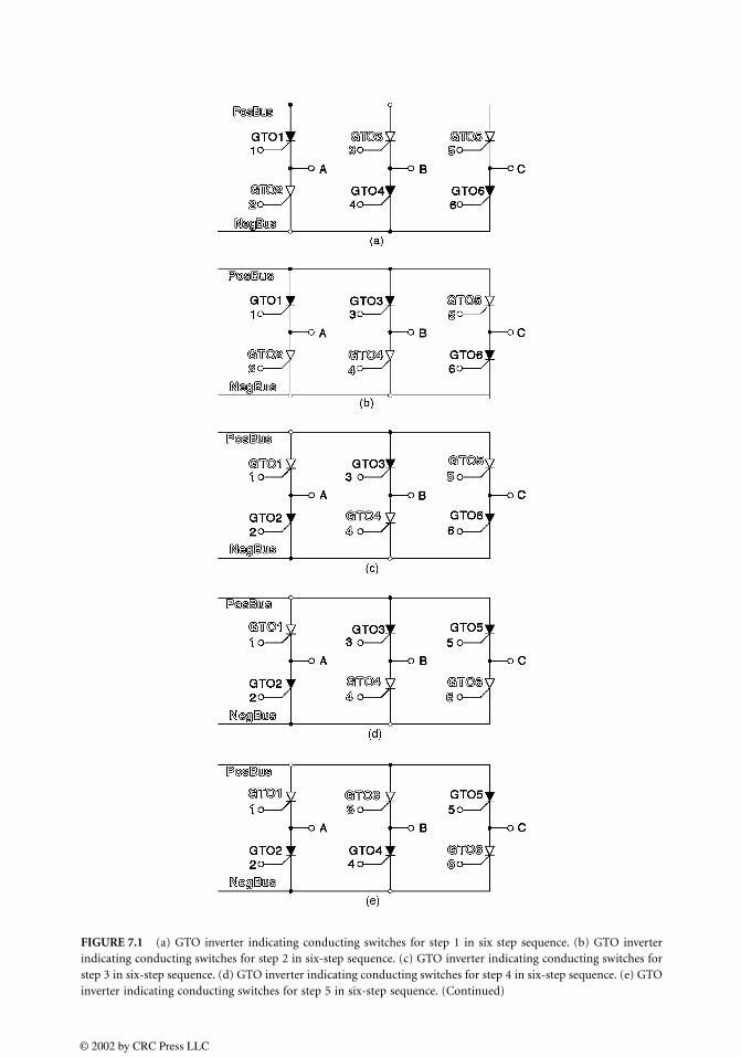
FIGURE 7.1 (a) GTO inverter indicating conducting switches for step 1 in six step sequence. (b) GTO inverterindicating conducting switches for step 2 in six-step sequence. (c) GTO inverter indicating conducting switches forstep 3 in six-step sequence. (d) GTO inverter indicating conducting switches for step 4 in six-step sequence. (e) GTOinverter indicating conducting switches for step 5 in six-step sequence. (Continued)
© 2002 by CRC Press LLC

FIGURE 7.1 (Continued.) (f) GTO inverter indicating conducting switches for step 6 in six-step sequence.
FIGURE 7.2 Graphical representation of the vector positions of the inverter states in a circle for six-step modulation.
FIGURE 7.3 Phase to neutral waveform of the inverter for six-step operation.
1
(f)
A
GTO13
B C
GTO3
6GTO6
© 2002 by CRC Press LLC
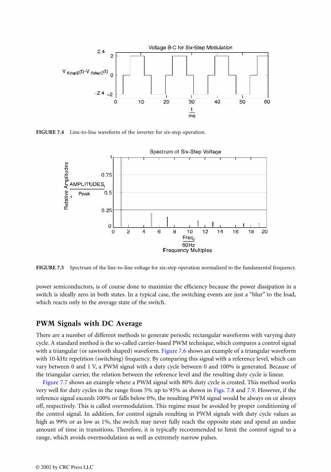
power semiconductors, is of course done to maximize the efficiency because the power dissipation in aswitch is ideally zero in both states. In a typical case, the switching events are just a “blur” to the load,which reacts only to the average state of the switch.
PWM Signals with DC Average
There are a number of different methods to generate periodic rectangular waveforms with varying dutycycle. A standard method is the so-called carrier-based PWM technique, which compares a control signalwith a triangular (or sawtooth shaped) waveform. Figure 7.6 shows an example of a triangular waveformwith 10-kHz repetition (switching) frequency. By comparing this signal with a reference level, which canvary between 0 and 1 V, a PWM signal with a duty cycle between 0 and 100% is generated. Because ofthe triangular carrier, the relation between the reference level and the resulting duty cycle is linear.
Figure 7.7 shows an example where a PWM signal with 80% duty cycle is created. This method worksvery well for duty cycles in the range from 5% up to 95% as shown in Figs. 7.8 and 7.9. However, if thereference signal exceeds 100% or falls below 0%, the resulting PWM signal would be always on or alwaysoff, respectively. This is called overmodulation. This regime must be avoided by proper conditioning ofthe control signal. In addition, for control signals resulting in PWM signals with duty cycle values ashigh as 99% or as low as 1%, the switch may never fully reach the opposite state and spend an undueamount of time in transitions. Therefore, it is typically recommended to limit the control signal to arange, which avoids overmodulation as well as extremely narrow pulses.
FIGURE 7.4 Line-to-line waveform of the inverter for six-step operation.
FIGURE 7.5 Spectrum of the line-to-line voltage for six-step operation normalized to the fundamental frequency.
© 2002 by CRC Press LLC
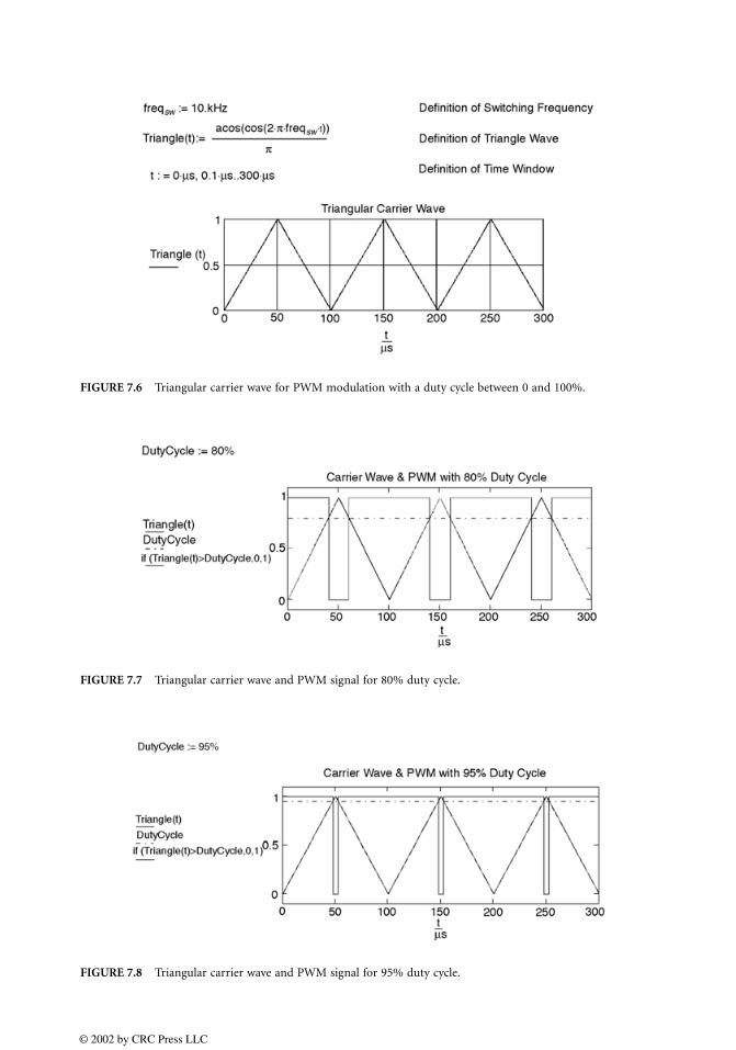
FIGURE 7.6 Triangular carrier wave for PWM modulation with a duty cycle between 0 and 100%.
FIGURE 7.7 Triangular carrier wave and PWM signal for 80% duty cycle.
FIGURE 7.8 Triangular carrier wave and PWM signal for 95% duty cycle.
© 2002 by CRC Press LLC
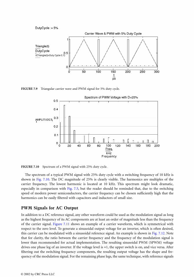
The spectrum of a typical PWM signal with 25% duty cycle with a switching frequency of 10 kHz isshown in Fig. 7.10. The DC magnitude of 25% is clearly visible. The harmonics are multiples of thecarrier frequency. The lowest harmonic is located at 10 kHz. This spectrum might look dramatic,especially in comparison with Fig. 7.5, but the reader should be reminded that, due to the switchingspeed of modern power semiconductors, the carrier frequency can be chosen sufficiently high that theharmonics can be easily filtered with capacitors and inductors of small size.
PWM Signals for AC Output
In addition to a DC reference signal, any other waveform could be used as the modulation signal as longas the highest frequency of its AC components are at least an order of magnitude less than the frequencyof the carrier signal. Figure 7.11 shows an example of a carrier waveform, which is symmetrical withrespect to the zero level. To generate a sinusoidal output voltage for an inverter, which is often desired,this carrier can be modulated with a sinusoidal reference signal. An example is shown in Fig. 7.12. Notethat for clarity, the ratio between the carrier frequency and the frequency of the modulation signal islower than recommended for actual implementation. The resulting sinusoidal PWM (SPWM) voltagedrives one phase leg of an inverter. If the voltage level is +1, the upper switch is on, and vice versa. Afterfiltering out the switching frequency components, the resulting output voltage has the shape and fre-quency of the modulation signal. For the remaining phase legs, the same technique, with reference signals
FIGURE 7.9 Triangular carrier wave and PWM signal for 5% duty cycle.
FIGURE 7.10 Spectrum of a PWM signal with 25% duty cycle.
© 2002 by CRC Press LLC
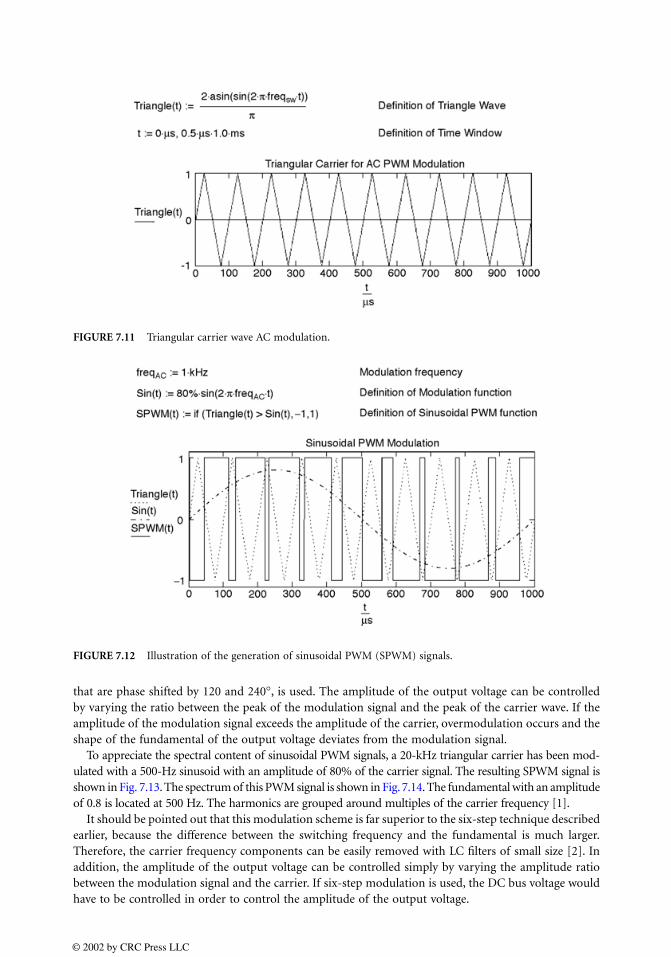
that are phase shifted by 120 and 240°, is used. The amplitude of the output voltage can be controlledby varying the ratio between the peak of the modulation signal and the peak of the carrier wave. If theamplitude of the modulation signal exceeds the amplitude of the carrier, overmodulation occurs and theshape of the fundamental of the output voltage deviates from the modulation signal.
To appreciate the spectral content of sinusoidal PWM signals, a 20-kHz triangular carrier has been mod-ulated with a 500-Hz sinusoid with an amplitude of 80% of the carrier signal. The resulting SPWM signal isshown in Fig. 7.13. The spectrum of this PWM signal is shown in Fig. 7.14. The fundamental with an amplitudeof 0.8 is located at 500 Hz. The harmonics are grouped around multiples of the carrier frequency [1].
It should be pointed out that this modulation scheme is far superior to the six-step technique describedearlier, because the difference between the switching frequency and the fundamental is much larger.Therefore, the carrier frequency components can be easily removed with LC filters of small size [2]. Inaddition, the amplitude of the output voltage can be controlled simply by varying the amplitude ratiobetween the modulation signal and the carrier. If six-step modulation is used, the DC bus voltage wouldhave to be controlled in order to control the amplitude of the output voltage.
FIGURE 7.11 Triangular carrier wave AC modulation.
FIGURE 7.12 Illustration of the generation of sinusoidal PWM (SPWM) signals.
© 2002 by CRC Press LLC
References
1. Mohan, N., Undeland, T., and Robbins, W., Power Electronics: Converters, Applications, and Design,2nd ed., John Wiley & Sons, New York, 1995.
2. Von Jouanne, A., Rendusara, D., Enjeti, P., and Gray, W., Filtering techniques to minimize the effectof long motor leads on PWM inverter fed AC motor drive systems, IEEE Trans. Ind. Appl., July/Aug.,919–926, 1996.
7.4 Third Harmonic Injection for Voltage Boost of SPWM Signals
Michael Giesselmann
It can be shown (Mohan et al.[1], p. 105) that if a three-phase input voltage is rectified using a standardthree-phase rectifier, the resulting DC voltage is equal to 1.35 times the rms value of the AC line–lineinput voltage. If this DC voltage is used to feed a three-phase inverter using the SPWM modulationtechnique described above, the theoretical maximum AC line–line output voltage is only 82.7% of theAC line–line input voltage feeding the rectifier (Mohan et al.[1], p. 228). To boost the output voltagewithout resorting to overmodulation, the third harmonic of the fundamental frequency can be added tothe modulation signal. Figure 7.15 shows an example, where a third harmonic with an amplitude of21.1% has been added to the fundamental modulation signal.
FIGURE 7.13 20-kHz carrier modulated with 500 Hz.
FIGURE 7.14 Spectrum of the SPWM signal shown in Fig. 7.13.
1
0.5
0
0.5
10 0.2 0.4 0.6 0.8 1 1.2 1.4 1.6 1.8 2
tms
SPWM(t)
Sin(t)
20-kHz carrier modulated with 500 Hz
© 2002 by CRC Press LLC
The amplitude of the fundamental has been increased to 112% in this example. It can be seen, thatthe peak amplitude of the resulting signal does not exceed the amplitude of the pure sinusoid with100% amplitude. By inspection of Fig. 7.15 it is easy to see that the voltage–time integral will be higherif a 3rd harmonic is added to the reference signal for the phase to neutral voltage. This voltage boostbeyond the previously mentioned value of 82.7% is very desirable, to retrofit induction motors withadjustable speed drives in existing installations. The 3rd harmonic components exactly cancel each otherin the line-to-line voltages of the inverter. This is because the phase shift of the fundamental signals is120° and therefore the phase shift of the 3rd harmonic is 3 × 120 = 360°. Therefore, the 3rd harmonicvoltages precisely cancel and result in a pure sinusoidal output voltage being applied to the motor. Thisis shown in Fig. 7.16, which illustrates the voltage boost that is obtained.
FIGURE 7.15 Sinusoidal modulation signal with and without added 3rd harmonic.
FIGURE 7.16 Line-to-line signal showing the voltage boost obtained by 3rd harmonic injection.
© 2002 by CRC Press LLC
Reference
1. Mohan, N., Undeland, T., and Robbins, W., Power Electronics: Converters, Applications, and Design,2nd ed., John Wiley & Sons, New York, 1995.
7.5 Generation of PWM Signals Using Microcontrollersand DSPs
Michael Giesselmann
Modern power electronics controllers are rapidly moving toward digital implementation. Typical solu-tions consist of microcontrollers or DSPs. In addition, coprocessors, such as the ADMC200/201 fromAnalog Devices, are available that are specifically designed to support inverter control. Most of theprocessors, such as the 68HC12B32 from Motorola, that are commonly used to control power electronicshave built-in hardware support for PWM generation. Figure 7.17 shows the basic principle of their digitalPWM generation.
For clarity, the circuit shown in Fig. 7.17 has only 4-bit resolution for the duty cycle of the generatedPWM signals, resulting in only 16 discrete duty cycles. In actual applications, 8 to 12 bits of resolutionis typical. In Fig. 7.17, a digital counter (74163) counts from zero to its maximum value and repeats thecycle afterward. The count is continuously compared with a digital value representing the duty cycleusing a hardware comparator (7485). The PWM signal is available on the output of the comparator.Figure 7.18 shows the simulation results from the example circuit shown in Fig. 7.17. The duty cycle inthis example is 3/16.
If more than one channel is present, the PWM signals can be left, right, or center aligned. To be centeraligned, up–down counters are used, which count up to their maximum count and then back to zerobefore starting the next cycle. The maximum count (2
bits − 1) is determined by the number of stages(bits) the digital counter has. In a digital PWM modulator each counter has an associated period register.The content of this register determines the maximum count at which the counter resets. If this numberis less than the maximum count (2
bits − 1), the repetition (switching) frequency is increased and the
FIGURE 7.17 Principle of digital PWM signal generation.
FIGURE 7.18 Simulation results from the circuit shown in Fig. 7.17.
© 2002 by CRC Press LLC
resolution of the duty cycle is decreased for a given clock speed. It is often important to make the correcttrade-off between the switching frequency and the resolution.
The advantage of hardware support for PWM generation is that the processor typically only needs toaccess any registers if the duty cycle is to be changed, since the period is typically only initialized onceupon program start-up. It should also be mentioned that the duty cycle registers are typically “double-buffered,” meaning that an update of a duty cycle does not need to be synchronized with the currentstate of the counter. In double-buffered systems, the new duty cycle will only be chosen once the previousperiod is completed to avoid truncated PWM signals. If necessary, a software override can disable thisfeature.
7.6 Voltage Source–Based Current Regulation
Michael Giesselmann
In motor drive applications, it is often desired to control directly the input current of the motor to controlthe torque. DC control also limits dynamics resulting from the electrical characteristics of the machine.Controlling the torque provides direct control over the angular acceleration, which is essential for precisemotion control. Current control is typically performed in the innermost loop of a cascaded feedbackcontrol loop arrangement [1]. However, most power electronics converters are circuits with controllablevoltage output. To achieve current control, the voltage of the power electronics converter can be controlledin such a way, that the desired current is obtained. Several methods can be used to achieve this:
• A feedback control loop, typically using a PI controller can be used control the current.
• The necessary voltage can be calculated in real time and applied to the motor.
• The necessary voltage for fast transients can be calculated in real time and applied to the motorand the residual error can be corrected by a PI controller.
Examples illustrating each of the schemes are described in the following. Figure 7.19 shows an exampleof a DC motor in which the current is controlled by adjusting the applied voltage using a PI controllersuch that the current follows the desired trajectory. The result is presented in Fig. 7.20, which shows thatthe current indeed follows the desired value at all times.
Sometimes even better results and higher loop bandwidth can be obtained if known information aboutthe motor and the load is used to calculate the required voltage in real time. Figure 7.21 shows somefundamental equations of a permanent magnet (PM) DC motor. Here a capacitor is used to representthe kinetic energy stored in the machine. Therefore, the second voltage loop equation in Fig. 7.21represents the voltage across the motor at all times. To test this theory, the “compensator” in the circuitshown in Fig. 7.22 calculates this voltage and applies the result to the DC motor. The subcircuit of the
FIGURE 7.19 Voltage source–based current control using a PI feedback loop.
© 2002 by CRC Press LLC
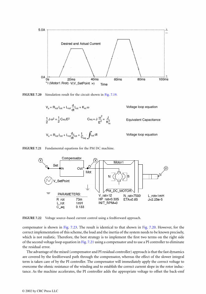
compensator is shown in Fig. 7.23. The result is identical to that shown in Fig. 7.20. However, for thecorrect implementation of this scheme, the load and the inertia of the system needs to be known precisely,which is not realistic. Therefore, the best strategy is to implement the first two terms on the right sideof the second voltage loop equation in Fig. 7.21 using a compensator and to use a PI controller to eliminatethe residual error.
The advantage of the mixed (compensator and PI residual controller) approach is that the fast dynamicsare covered by the feedforward path through the compensator, whereas the effect of the slower integralterm is taken care of by the PI controller. The compensator will immediately apply the correct voltage toovercome the ohmic resistance of the winding and to establish the correct current slope in the rotor induc-tance. As the machine accelerates, the PI controller adds the appropriate voltage to offset the back-emf
FIGURE 7.20 Simulation result for the circuit shown in Fig. 7.19.
FIGURE 7.21 Fundamental equations for the PM DC machine.
FIGURE 7.22 Voltage source–based current control using a feedforward approach.
Voltage loop equation
Equivalent Capacitance
Voltage loop equation
Vs = Rrot⋅Irot + Lrot⋅ − Irot + Km⋅ω ddt
Vs = Rrot⋅Irot + Lrot⋅−Irot + −⋅ddt
Irot dt
−⋅J⋅ω2 = −⋅Ceq⋅E212
12
Ceq = J⋅ = ω2
E2JKm
1Ceq
2
© 2002 by CRC Press LLC
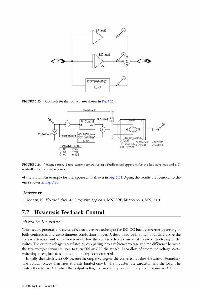
of the motor. An example for this approach is shown in Fig. 7.24. Again, the results are identical to theones shown in Fig. 7.20.
Reference
1. Mohan, N., Electric Drives, An Integrative Approach, MNPERE, Minneapolis, MN, 2001.
7.7 Hysteresis Feedback Control
Hossein Salehfar
This section presents a hysteresis feedback control technique for DC-DC buck converters operating inboth continuous and discontinuous conduction modes. A dead band with a high boundary above thevoltage reference and a low boundary below the voltage reference are used to avoid chattering in theswitch. The output voltage is regulated by comparing it to a reference voltage and the difference betweenthe two voltages (error) is used to turn ON or OFF the switch. Regardless of where the voltage starts,switching takes place as soon as a boundary is encountered.
Initially, the switch turns ON because the output voltage of the converter is below the turn-on boundary.The output voltage then rises at a rate limited only by the inductor, the capacitor, and the load. Theswitch then turns OFF when the output voltage crosses the upper boundary and it remains OFF until
FIGURE 7.23 Subcircuit for the compensator shown in Fig. 7.22.
FIGURE 7.24 Voltage source–based current control using a feedforward approach for the fast transients and a PIcontroller for the residual error.
© 2002 by CRC Press LLC
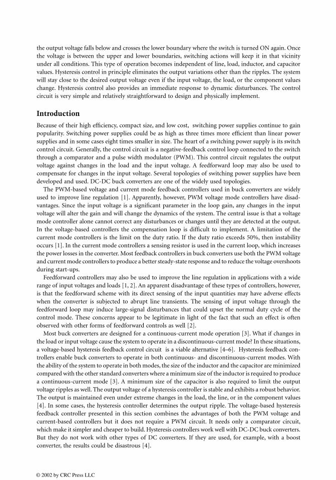
the output voltage falls below and crosses the lower boundary where the switch is turned ON again. Oncethe voltage is between the upper and lower boundaries, switching actions will keep it in that vicinityunder all conditions. This type of operation becomes independent of line, load, inductor, and capacitorvalues. Hysteresis control in principle eliminates the output variations other than the ripples. The systemwill stay close to the desired output voltage even if the input voltage, the load, or the component valueschange. Hysteresis control also provides an immediate response to dynamic disturbances. The controlcircuit is very simple and relatively straightforward to design and physically implement.
Introduction
Because of their high efficiency, compact size, and low cost, switching power supplies continue to gainpopularity. Switching power supplies could be as high as three times more efficient than linear powersupplies and in some cases eight times smaller in size. The heart of a switching power supply is its switchcontrol circuit. Generally, the control circuit is a negative-feedback control loop connected to the switchthrough a comparator and a pulse width modulator (PWM). This control circuit regulates the outputvoltage against changes in the load and the input voltage. A feedforward loop may also be used tocompensate for changes in the input voltage. Several topologies of switching power supplies have beendeveloped and used. DC-DC buck converters are one of the widely used topologies.
The PWM-based voltage and current mode feedback controllers used in buck converters are widelyused to improve line regulation [1]. Apparently, however, PWM voltage mode controllers have disad-vantages. Since the input voltage is a significant parameter in the loop gain, any changes in the inputvoltage will alter the gain and will change the dynamics of the system. The central issue is that a voltagemode controller alone cannot correct any disturbances or changes until they are detected at the output.In the voltage-based controllers the compensation loop is difficult to implement. A limitation of thecurrent mode controllers is the limit on the duty ratio. If the duty ratio exceeds 50%, then instabilityoccurs [1]. In the current mode controllers a sensing resistor is used in the current loop, which increasesthe power losses in the converter. Most feedback controllers in buck converters use both the PWM voltageand current mode controllers to produce a better steady-state response and to reduce the voltage overshootsduring start-ups.
Feedforward controllers may also be used to improve the line regulation in applications with a widerange of input voltages and loads [1, 2]. An apparent disadvantage of these types of controllers, however,is that the feedforward scheme with its direct sensing of the input quantities may have adverse effectswhen the converter is subjected to abrupt line transients. The sensing of input voltage through thefeedforward loop may induce large-signal disturbances that could upset the normal duty cycle of thecontrol mode. These concerns appear to be legitimate in light of the fact that such an effect is oftenobserved with other forms of feedforward controls as well [2].
Most buck converters are designed for a continuous-current mode operation [3]. What if changes inthe load or input voltage cause the system to operate in a discontinuous-current mode? In these situations,a voltage-based hysteresis feedback control circuit is a viable alternative [4–6]. Hysteresis feedback con-trollers enable buck converters to operate in both continuous- and discontinuous-current modes. Withthe ability of the system to operate in both modes, the size of the inductor and the capacitor are minimizedcompared with the other standard converters where a minimum size of the inductor is required to producea continuous-current mode [3]. A minimum size of the capacitor is also required to limit the outputvoltage ripples as well. The output voltage of a hysteresis controller is stable and exhibits a robust behavior.The output is maintained even under extreme changes in the load, the line, or in the component values[4]. In some cases, the hysteresis controller determines the output ripple. The voltage-based hysteresisfeedback controller presented in this section combines the advantages of both the PWM voltage andcurrent-based controllers but it does not require a PWM circuit. It needs only a comparator circuit,which make it simpler and cheaper to build. Hysteresis controllers work well with DC-DC buck converters.But they do not work with other types of DC converters. If they are used, for example, with a boostconverter, the results could be disastrous [4].
© 2002 by CRC Press LLC
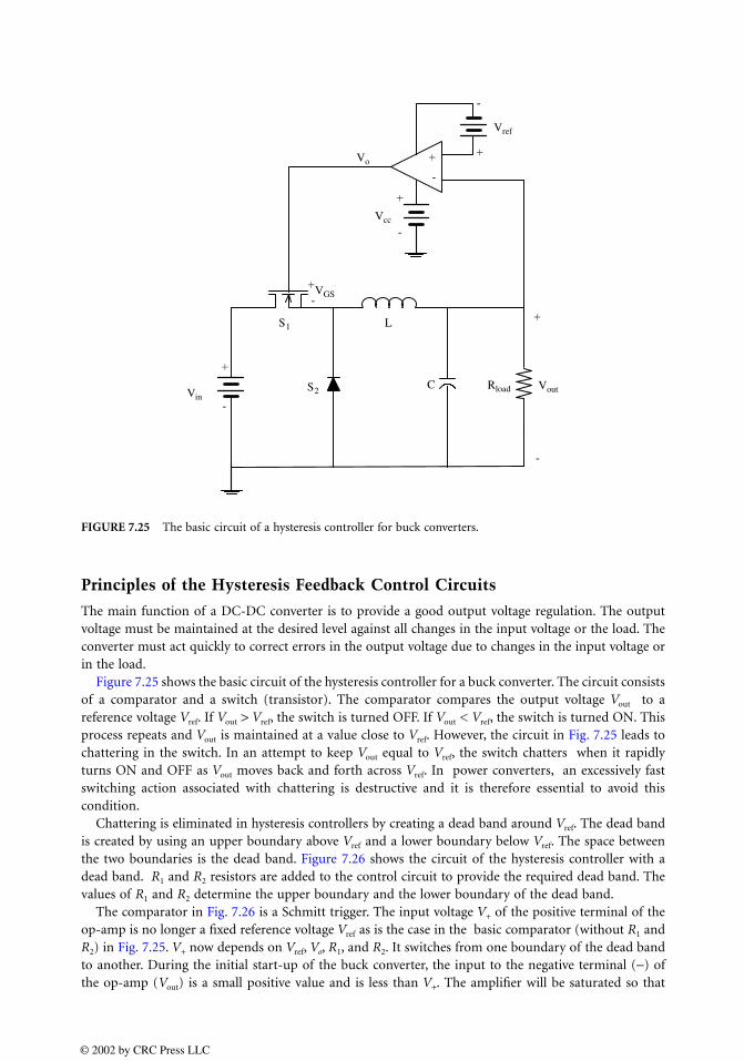
Principles of the Hysteresis Feedback Control Circuits
The main function of a DC-DC converter is to provide a good output voltage regulation. The outputvoltage must be maintained at the desired level against all changes in the input voltage or the load. Theconverter must act quickly to correct errors in the output voltage due to changes in the input voltage orin the load.
Figure 7.25 shows the basic circuit of the hysteresis controller for a buck converter. The circuit consistsof a comparator and a switch (transistor). The comparator compares the output voltage Vout to areference voltage Vref. If Vout > Vref, the switch is turned OFF. If Vout < Vref, the switch is turned ON. Thisprocess repeats and Vout is maintained at a value close to Vref. However, the circuit in Fig. 7.25 leads tochattering in the switch. In an attempt to keep Vout equal to Vref, the switch chatters when it rapidlyturns ON and OFF as Vout moves back and forth across Vref. In power converters, an excessively fastswitching action associated with chattering is destructive and it is therefore essential to avoid thiscondition.
Chattering is eliminated in hysteresis controllers by creating a dead band around Vref. The dead bandis created by using an upper boundary above Vref and a lower boundary below Vref. The space betweenthe two boundaries is the dead band. Figure 7.26 shows the circuit of the hysteresis controller with adead band. R1 and R2 resistors are added to the control circuit to provide the required dead band. Thevalues of R1 and R2 determine the upper boundary and the lower boundary of the dead band.
The comparator in Fig. 7.26 is a Schmitt trigger. The input voltage V+ of the positive terminal of theop-amp is no longer a fixed reference voltage Vref as is the case in the basic comparator (without R1 andR2) in Fig. 7.25. V+ now depends on Vref, Vo, R1, and R2. It switches from one boundary of the dead bandto another. During the initial start-up of the buck converter, the input to the negative terminal (−) ofthe op-amp (Vout) is a small positive value and is less than V+. The amplifier will be saturated so that
FIGURE 7.25 The basic circuit of a hysteresis controller for buck converters.
+
-
-
Vcc
Vref
LS1
S2Vin
+
-
+-
++Vo
+
-
VGS
C Rload Vout
-
© 2002 by CRC Press LLC
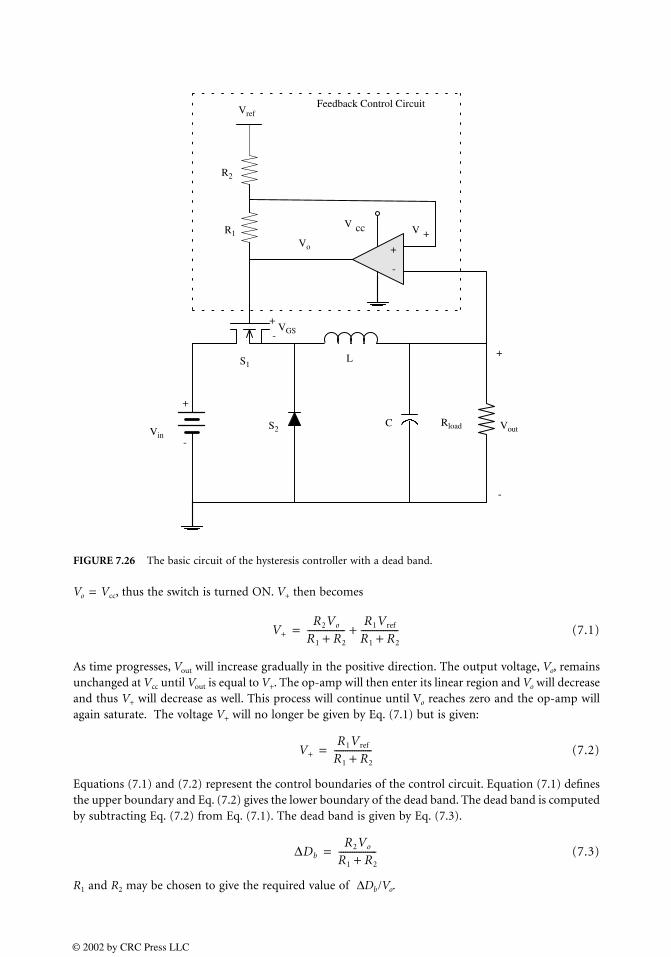
Vo = Vcc, thus the switch is turned ON. V+ then becomes
(7.1)
As time progresses, Vout will increase gradually in the positive direction. The output voltage, Vo, remainsunchanged at Vcc until Vout is equal to V+. The op-amp will then enter its linear region and Vo will decreaseand thus V+ will decrease as well. This process will continue until Vo reaches zero and the op-amp willagain saturate. The voltage V+ will no longer be given by Eq. (7.1) but is given:
(7.2)
Equations (7.1) and (7.2) represent the control boundaries of the control circuit. Equation (7.1) definesthe upper boundary and Eq. (7.2) gives the lower boundary of the dead band. The dead band is computedby subtracting Eq. (7.2) from Eq. (7.1). The dead band is given by Eq. (7.3).
(7.3)
R1 and R2 may be chosen to give the required value of ∆Db /Vo.
FIGURE 7.26 The basic circuit of the hysteresis controller with a dead band.
+
-
+
-
V cc
Vref
L
C
R1
R2
Rload
S1
S2 VoutVin
+
-
+
-VGS
Vo
V +
Feedback Control Circuit
V+R2Vo
R1 R2+-----------------
R1Vref
R1 R2+-----------------+=
V+R1Vref
R1 R2+-----------------=
∆Db
R2Vo
R1 R2+-----------------=
© 2002 by CRC Press LLC
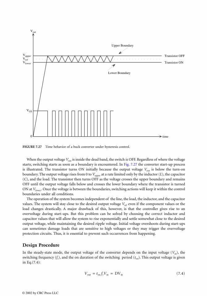
When the output voltage Vout is inside the dead band, the switch is OFF. Regardless of where the voltagestarts, switching starts as soon as a boundary is encountered. In Fig. 7.27 the converter start-up processis illustrated. The transistor turns ON initially because the output voltage Vout is below the turn-onboundary. The output voltage rises from 0 to Vupper at a rate limited only by the inductor (L), the capacitor(C), and the load. The transistor then turns OFF as the voltage crosses the upper boundary and remainsOFF until the output voltage falls below and crosses the lower boundary where the transistor is turnedON at Vlower . Once the voltage is between the boundaries, switching actions will keep it within the controlboundaries under all conditions.
The operation of the system becomes independent of the line, the load, the inductor, and the capacitorvalues. The system will stay close to the desired output voltage Vref even if the component values or theload changes drastically. A major drawback of this, however, is that the controller gives rise to anovervoltage during start-ups. But this problem can be solved by choosing the correct inductor andcapacitor values that will allow the system to rise exponentially and settle somewhat close to the desiredoutput voltage, while maintaining the desired ripple voltage. Initial voltage overshoots during start-upscan sometimes damage loads that are sensitive to high voltages or they may trigger the overvoltageprotection circuits. Thus, it is essential to prevent such occurrences from happening.
Design Procedure
In the steady-state mode, the output voltage of the converter depends on the input voltage (Vin), theswitching frequency (fs), and the on duration of the switching period (ton). This output voltage is givenin Eq.(7.4):
(7.4)
FIGURE 7.27 Time behavior of a buck converter under hysteresis control.
0
Vout
VupperVrefVlower
VGS
time
Lower Boundary
Transistor OFF
Transistor ON
Upper Boundary
Vout ton fs= Vin DVin=
© 2002 by CRC Press LLC

The product ton fs is defined as the duty ratio D. The output voltage Vout is regulated by changing D whilefs is kept constant. This method is widely used in DC-DC converters. Another approach to regulatingVout is to vary fs and keep D constant. However, this method is undesirable because it is difficult to filterthe ripples in the input and output signals of the converter.
The hysteresis control of the buck converter is a fixed boundary control. Vout is regulated by theswitching action of the switch as Vout crosses the upper or the lower boundary of the dead band of thehysteresis. In the hysteresis control of converters, fs as well as D are not fixed values, but they change withthe converter conditions. For a given set of converter parameters, both fs and D are determined by theboundaries of the hysteresis. The frequency fs and the duty ratio D are not used as control parametersin the design of hysteresis controllers. However, using a hysteresis controller, the basic operating principlesof the buck converter do not change. The output voltage ripples of the converter depend on the deadband of the controller. As the dead band increases or decreases, the output voltage ripples will increaseor decrease as well. The voltage ripple specifications can be guaranteed by setting the dead band of thecontroller at 50% of the ripple specifications with a suitable inductor value.
A properly designed hysteresis controller has excellent steady-state and dynamic properties. Its responsequickly changes from its starting point to its desired operating value. Fixed boundary controllers havesome important operating advantages. These controllers are stable under extreme disturbance conditionsand can be chosen to directly guarantee the ripple specifications or other operating issues in a converter.The implementation of the hysteresis controller is illustrated by a design example.
Design Example
A DC-DC buck converter with voltage-based hysteresis control is designed to verify the method discussedin this section. Let Vout = 5 V and let the load vary between 1 and 5 Ω. The input voltage Vin also variesbetween 16 and 24 V with a nominal value of 20 V. The maximum ripple voltage is set at ±1%. A nominalswitching frequency of fs = 100 kHz is chosen. The output voltage ripple is then
(7.5)
The dead band is chosen to be 50% of the output voltage ripple to account for the small increase inthe ripple level due to the natural response of the RLC circuit of the converter, after the switch is turnedOFF, and to meet the required voltage ripple specification. The system will not meet the voltage ripplespecification if the dead band is chosen to be equal to the output voltage ripple. The dead band is then
(7.6)
Eq. (7.3) is solved for R1:
(7.7)
Let R2 = 100 Ω and Vo = 10 V. Then R1 is
R1 = 100(10/0.05 − 1) = 19900 Ω
These resistor values produce a dead band that meets the output ripple specification. The maximum andminimum values of the load current are
Iout,max = Vout/Rmin = 5/1 = 5 A (7.8)
∆Vout
Vout
------------- 2%=
∆Vout 0.02 5× 0.1 V= =
∆Db 0.5 0.1× 0.05 V= =
R1 R2
Vo
∆Db
---------- 1– =
© 2002 by CRC Press LLC

and
Iout,min = Vout/Rmax = 5/5 = 1 A (7.9)
Let the inductor current and the capacitor voltage swings be 10%. The inductor must limit the currentswing at maximum load. The total current swing is as follows. Since
using Eq. (7.8), Iout,max = 5 A, then
(7.10)
The capacitor voltage swing is
(7.11)
The equivalent series resistance (ESR) of the capacitor C must be included in the calculations. Since thewaveform of the output ripple voltage is approximately sinusoidal, the output ripple voltage is then
(7.12)
where ∆VRC is the voltage ripple across the capacitor resistance RC. Note that ∆VRC is usually muchgreater than ∆Vc. Thus a close approximation of the peak-to-peak output voltage ripple is obtained asfollows:
(7.13)
With the result from Eq. (7.10), the inductor L is
(7.14)
The value of the capacitor is
(7.15)
The value of ESR of the capacitor can be determined from Eq. (7.13):
(7.16)
∆IL
Iout,max
-------------- 10%=
∆IL 0.1 5× 0.5 A= =
∆Vc
∆Vout
------------- 10%=
∆Vc 0.1 0.1× 0.01V= =
∆Vout ∆Vc( )2 ∆VRC( )2+=
∆Vout ∆VRC≅∆IcRc≅∆IL ∆IR–( )Rc≅
LVout Vin Vout–( )
Vin fs∆IL
------------------------------------ 5 20 5–( )20 100000( )0.5----------------------------------- 75 mH= = =
C∆IL
8fs∆Vc
---------------- 0.58 100000( )0.01----------------------------------- 62.5mF 65mF≅= = =
RC
∆Vout
∆IL ∆IR–---------------------- 0.1
0.5 0.1–-------------------- 0.25 Ω= = =
© 2002 by CRC Press LLC
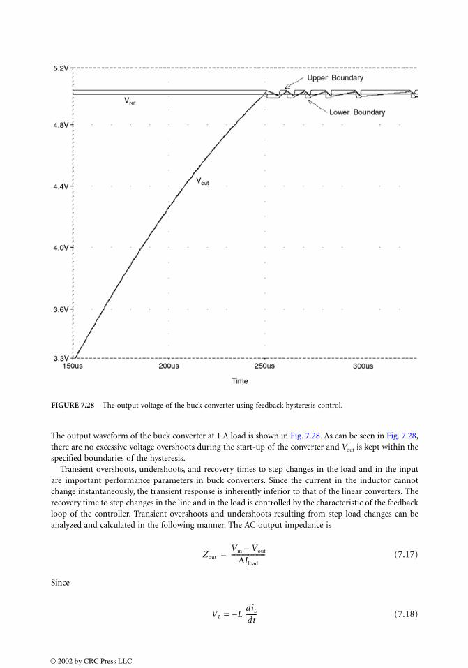
The output waveform of the buck converter at 1 A load is shown in Fig. 7.28. As can be seen in Fig. 7.28,there are no excessive voltage overshoots during the start-up of the converter and Vout is kept within thespecified boundaries of the hysteresis.
Transient overshoots, undershoots, and recovery times to step changes in the load and in the inputare important performance parameters in buck converters. Since the current in the inductor cannotchange instantaneously, the transient response is inherently inferior to that of the linear converters. Therecovery time to step changes in the line and in the load is controlled by the characteristic of the feedbackloop of the controller. Transient overshoots and undershoots resulting from step load changes can beanalyzed and calculated in the following manner. The AC output impedance is
(7.17)
Since
(7.18)
FIGURE 7.28 The output voltage of the buck converter using feedback hysteresis control.
Zout
Vin Vout–∆Iload
----------------------=
VL −L= diL
dt-------
© 2002 by CRC Press LLC

and
(7.19)
thus,
(7.20)
As a result, for an increasing current, the change in the output voltage will be as follows:
(7.21)
and for a decreasing current, the change in the output voltage is
(7.22)
The transient undershoot for a load change from 1 to 5 A can be determined from Eq. (7.21).
(7.23)
The transient overshoot for the load change from 5 to 1 A can be determined using Eq. (7.22).
(7.24)
Simulation Results
A DC-DC buck converter with a hysteresis feedback control circuit is constructed and simulated usingthe PSpice program. The results of the simulation were then compared to the theoretical results obtainedin Eqs. (7.23) and (7.24) above. Figure 7.29 shows the results from the simulation. The transient behaviorof the output voltage and the current of the converter can be obtained from Fig. 7.29. The maximumtransient overshoot voltage for a load change from 5 to 1 A is found to be
(7.25)
and the minimum transient undershoot voltage for a load change from 1 to 5 A is
(7.26)
These results show that the controller has significantly reduced the overshoot transient. The overshootvalue from the simulation is 36.47% of the theoretical value obtained using Eq. (7.24). However, a smallincrease in the undershoot transient is observed. The undershoot value from the simulation increasedby 24.1% compared to the value obtained from Eq. (7.23). One can also see that the system has gonefrom a continuous-current mode to a discontinuous-current mode and back to a continuous-currentmode. The switch is turned OFF when the output voltage crosses the upper boundary. The system thendegrades linearly until it is back into a continuous-current mode where the switch is turned ON againand it continues its switching operation within the continuous-current mode region.
Iout C = dvdt-----
Zout
L∆Iout
Vin Vout–( )C-------------------------------=
∆Vout,min ∆IoutZout
L∆Iout2
Vin Vout–( )C-------------------------------= =
∆Vout,max
L∆Iout2
VoutC--------------=
∆Vout,min
L∆Iout2
Vin Vout–( )C------------------------------- 0.000075 5 1–( )2
20 5–( )0.000065----------------------------------------- 1.231 V= = =
∆Vout,max
L∆Iout2
VoutC-------------- 0.000075 5 1–( )2
5 0.000065( )---------------------------------------- 3.692 V= = =
∆Vout,max 6.3463= 5– 1.3463 V=
∆Vout,min 5.0 3.4724– 1.5276 V= =
© 2002 by CRC Press LLC
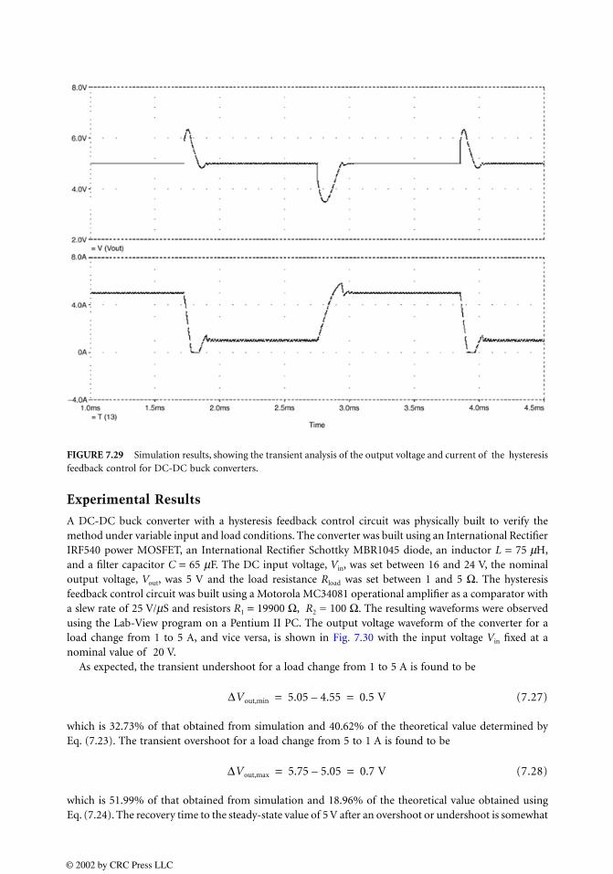
Experimental Results
A DC-DC buck converter with a hysteresis feedback control circuit was physically built to verify themethod under variable input and load conditions. The converter was built using an International RectifierIRF540 power MOSFET, an International Rectifier Schottky MBR1045 diode, an inductor L = 75 µH,and a filter capacitor C = 65 µF. The DC input voltage, Vin, was set between 16 and 24 V, the nominaloutput voltage, Vout, was 5 V and the load resistance Rload was set between 1 and 5 Ω. The hysteresisfeedback control circuit was built using a Motorola MC34081 operational amplifier as a comparator witha slew rate of 25 V/µS and resistors R1 = 19900 Ω, R2 = 100 Ω. The resulting waveforms were observedusing the Lab-View program on a Pentium II PC. The output voltage waveform of the converter for aload change from 1 to 5 A, and vice versa, is shown in Fig. 7.30 with the input voltage Vin fixed at anominal value of 20 V.
As expected, the transient undershoot for a load change from 1 to 5 A is found to be
(7.27)
which is 32.73% of that obtained from simulation and 40.62% of the theoretical value determined byEq. (7.23). The transient overshoot for a load change from 5 to 1 A is found to be
(7.28)
which is 51.99% of that obtained from simulation and 18.96% of the theoretical value obtained usingEq. (7.24). The recovery time to the steady-state value of 5 V after an overshoot or undershoot is somewhat
FIGURE 7.29 Simulation results, showing the transient analysis of the output voltage and current of the hysteresisfeedback control for DC-DC buck converters.
∆Vout,min 5.05 4.55– 0.5 V= =
∆Vout,max 5.75 5.05– 0.7 V= =
© 2002 by CRC Press LLC
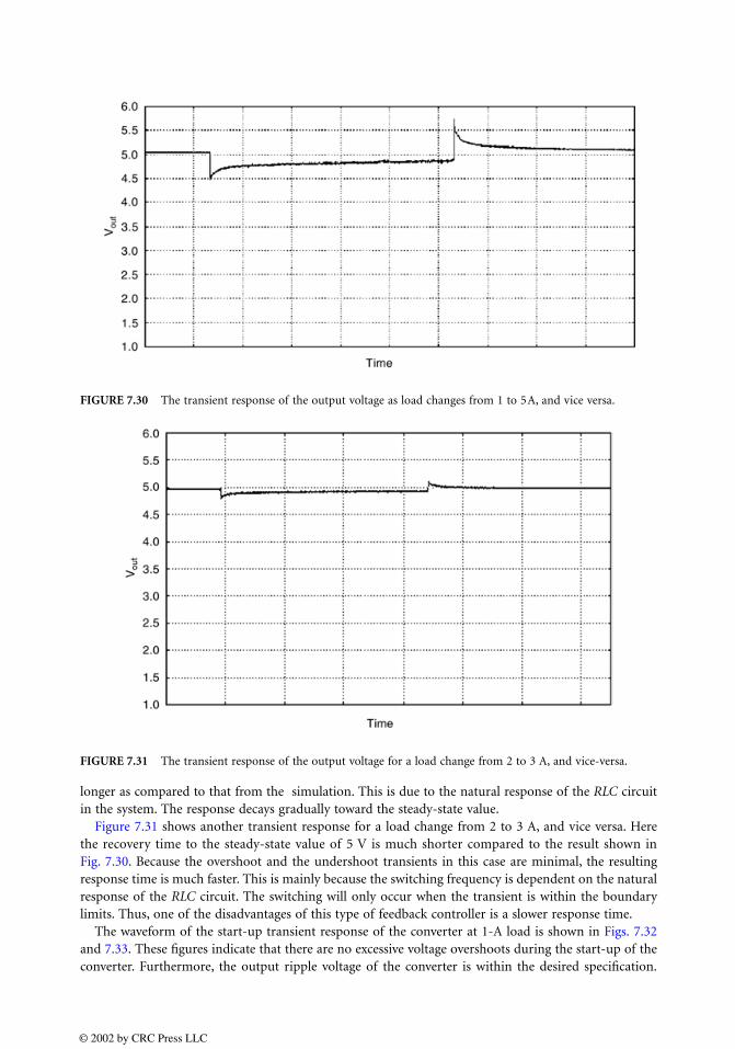
longer as compared to that from the simulation. This is due to the natural response of the RLC circuitin the system. The response decays gradually toward the steady-state value.
Figure 7.31 shows another transient response for a load change from 2 to 3 A, and vice versa. Herethe recovery time to the steady-state value of 5 V is much shorter compared to the result shown inFig. 7.30. Because the overshoot and the undershoot transients in this case are minimal, the resultingresponse time is much faster. This is mainly because the switching frequency is dependent on the naturalresponse of the RLC circuit. The switching will only occur when the transient is within the boundarylimits. Thus, one of the disadvantages of this type of feedback controller is a slower response time.
The waveform of the start-up transient response of the converter at 1-A load is shown in Figs. 7.32and 7.33. These figures indicate that there are no excessive voltage overshoots during the start-up of theconverter. Furthermore, the output ripple voltage of the converter is within the desired specification.
FIGURE 7.30 The transient response of the output voltage as load changes from 1 to 5A, and vice versa.
FIGURE 7.31 The transient response of the output voltage for a load change from 2 to 3 A, and vice-versa.
© 2002 by CRC Press LLC
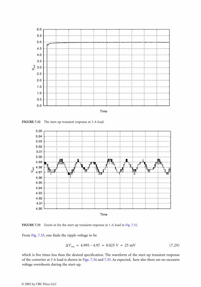
From Fig. 7.33, one finds the ripple voltage to be
(7.29)
which is five times less than the desired specification. The waveform of the start-up transient responseof the converter at 5 A load is shown in Figs. 7.34 and 7.35. As expected, here also there are no excessivevoltage overshoots during the start-up.
FIGURE 7.32 The start-up transient response at 1-A load.
FIGURE 7.33 Zoom-in for the start-up transient response at 1-A load in Fig. 7.32.
∆Vout 4.995 4.97– 0.025 V 25 mV= = =
© 2002 by CRC Press LLC
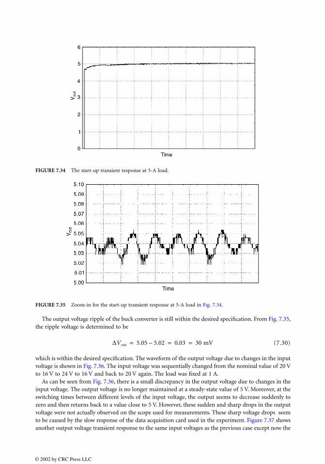
The output voltage ripple of the buck converter is still within the desired specification. From Fig. 7.35,the ripple voltage is determined to be
(7.30)
which is within the desired specification. The waveform of the output voltage due to changes in the inputvoltage is shown in Fig. 7.36. The input voltage was sequentially changed from the nominal value of 20 Vto 16 V to 24 V to 16 V and back to 20 V again. The load was fixed at 1 A.
As can be seen from Fig. 7.36, there is a small discrepancy in the output voltage due to changes in theinput voltage. The output voltage is no longer maintained at a steady-state value of 5 V. Moreover, at theswitching times between different levels of the input voltage, the output seems to decrease suddenly tozero and then returns back to a value close to 5 V. However, these sudden and sharp drops in the outputvoltage were not actually observed on the scope used for measurements. These sharp voltage drops seemto be caused by the slow response of the data acquisition card used in the experiment. Figure 7.37 showsanother output voltage transient response to the same input voltages as the previous case except now the
FIGURE 7.34 The start-up transient response at 5-A load.
FIGURE 7.35 Zoom-in for the start-up transient response at 5-A load in Fig. 7.34.
∆Vout 5.05 5.02– 0.03 30 mV= = =
© 2002 by CRC Press LLC
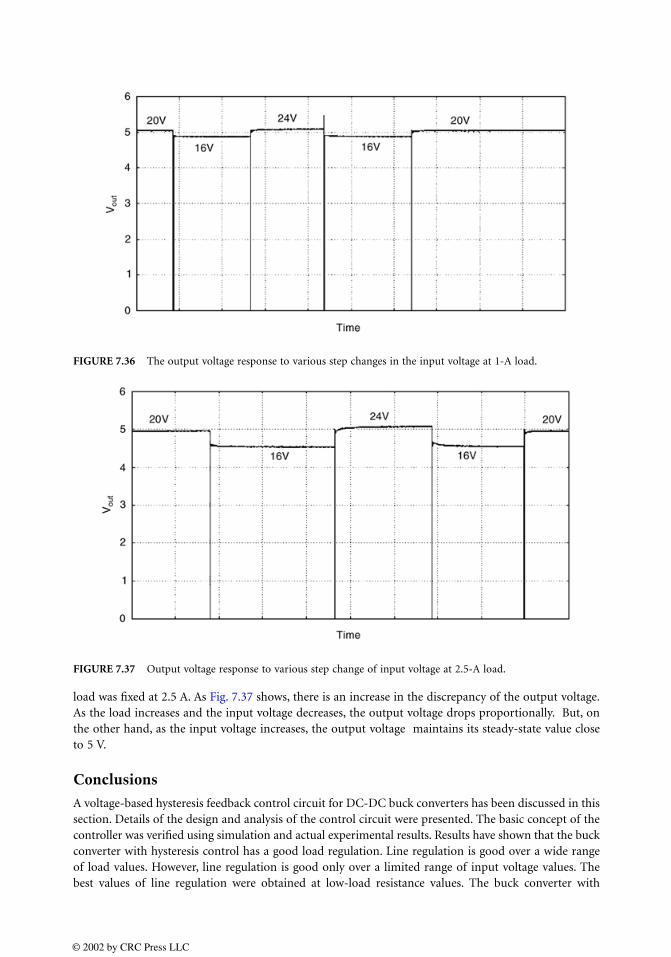
load was fixed at 2.5 A. As Fig. 7.37 shows, there is an increase in the discrepancy of the output voltage.As the load increases and the input voltage decreases, the output voltage drops proportionally. But, onthe other hand, as the input voltage increases, the output voltage maintains its steady-state value closeto 5 V.
Conclusions
A voltage-based hysteresis feedback control circuit for DC-DC buck converters has been discussed in thissection. Details of the design and analysis of the control circuit were presented. The basic concept of thecontroller was verified using simulation and actual experimental results. Results have shown that the buckconverter with hysteresis control has a good load regulation. Line regulation is good over a wide rangeof load values. However, line regulation is good only over a limited range of input voltage values. Thebest values of line regulation were obtained at low-load resistance values. The buck converter with
FIGURE 7.36 The output voltage response to various step changes in the input voltage at 1-A load.
FIGURE 7.37 Output voltage response to various step change of input voltage at 2.5-A load.
© 2002 by CRC Press LLC
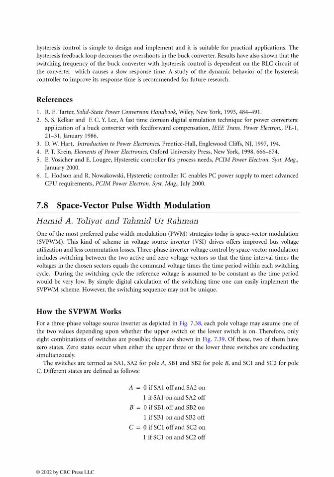
hysteresis control is simple to design and implement and it is suitable for practical applications. Thehysteresis feedback loop decreases the overshoots in the buck converter. Results have also shown that theswitching frequency of the buck converter with hysteresis control is dependent on the RLC circuit ofthe converter which causes a slow response time. A study of the dynamic behavior of the hysteresiscontroller to improve its response time is recommended for future research.
References
1. R. E. Tarter, Solid-State Power Conversion Handbook, Wiley, New York, 1993, 484–491.2. S. S. Kelkar and F. C. Y. Lee, A fast time domain digital simulation technique for power converters:
application of a buck converter with feedforward compensation, IEEE Trans. Power Electron., PE-1,21–31, January 1986.
3. D. W. Hart, Introduction to Power Electronics, Prentice-Hall, Englewood Cliffs, NJ, 1997, 194.4. P. T. Krein, Elements of Power Electronics, Oxford University Press, New York, 1998, 666–674.5. E. Vosicher and E. Lougee, Hysteretic controller fits process needs, PCIM Power Electron. Syst. Mag.,
January 2000.6. L. Hodson and R. Nowakowski, Hysteretic controller IC enables PC power supply to meet advanced
CPU requirements, PCIM Power Electron. Syst. Mag., July 2000.
7.8 Space-Vector Pulse Width Modulation
Hamid A. Toliyat and Tahmid Ur Rahman
One of the most preferred pulse width modulation (PWM) strategies today is space-vector modulation(SVPWM). This kind of scheme in voltage source inverter (VSI) drives offers improved bus voltageutilization and less commutation losses. Three-phase inverter voltage control by space-vector modulationincludes switching between the two active and zero voltage vectors so that the time interval times thevoltages in the chosen sectors equals the command voltage times the time period within each switchingcycle. During the switching cycle the reference voltage is assumed to be constant as the time periodwould be very low. By simple digital calculation of the switching time one can easily implement theSVPWM scheme. However, the switching sequence may not be unique.
How the SVPWM Works
For a three-phase voltage source inverter as depicted in Fig. 7.38, each pole voltage may assume one ofthe two values depending upon whether the upper switch or the lower switch is on. Therefore, onlyeight combinations of switches are possible; these are shown in Fig. 7.39. Of these, two of them havezero states. Zero states occur when either the upper three or the lower three switches are conductingsimultaneously.
The switches are termed as SA1, SA2 for pole A, SB1 and SB2 for pole B, and SC1 and SC2 for poleC. Different states are defined as follows:
A 0 if SA1 off and SA2 on=1 if SA1 on and SA2 off
B 0 if SB1 off and SB2 on=1 if SB1 on and SB2 off
C 0 if SC1 off and SC2 on=1 if SC1 on and SC2 off
© 2002 by CRC Press LLC
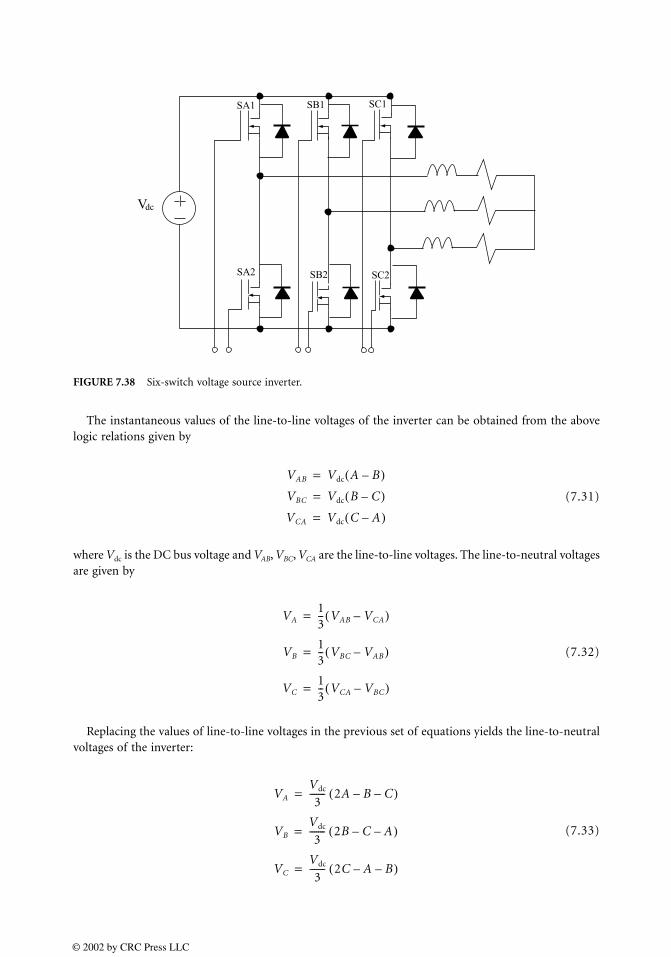
The instantaneous values of the line-to-line voltages of the inverter can be obtained from the abovelogic relations given by
(7.31)
where Vdc is the DC bus voltage and VAB, VBC, VCA are the line-to-line voltages. The line-to-neutral voltagesare given by
(7.32)
Replacing the values of line-to-line voltages in the previous set of equations yields the line-to-neutralvoltages of the inverter:
(7.33)
FIGURE 7.38 Six-switch voltage source inverter.
SC1
SB2
SA1 SB1
SC2SA2
Vdc
VAB Vdc A B–( )=VBC Vdc B C–( )=VCA Vdc C A–( )=
VA13-- VAB VCA–( )=
VB13-- VBC VAB–( )=
VC13-- VCA VBC–( )=
VA
Vdc
3------- 2A B– C–( )=
VB
Vdc
3------- 2B C– A–( )=
VC
Vdc
3------- 2C A– B–( )=
© 2002 by CRC Press LLC
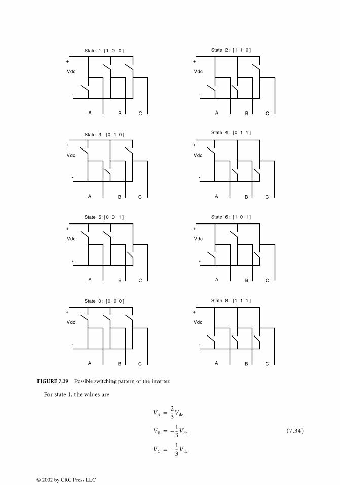
For state 1, the values are
(7.34)
FIGURE 7.39 Possible switching pattern of the inverter.
A B C
Vdc
+
-
A B C
Vdc
+
-
A B C
Vdc
+
-
A B C
Vdc
+
-
A B C
Vdc
+
-
A B C
Vdc
+
-
A B C
Vdc
+
-
A B C
Vdc
+
-
State 1 : [1 0 0 ]
State 3 : [0 1 0 ]
State 5 : [0 0 1 ]
State 0 : [0 0 0 ]
State 2 : [1 1 0 ]
State 4 : [0 1 1 ]
State 6 : [1 0 1 ]
State 8 : [1 1 1 ]
VA23--Vdc=
VB13--Vdc–=
VC13--Vdc–=
© 2002 by CRC Press LLC

By using the following transformation for a balanced three-phase system, the space vector for sector1 with α and β components is given by
(7.35)
Therefore, for the first sector space vector Vs1 will be given by
(7.36)
All the other six nonzero states are given by
(7.37)
where the values of k vary from 1 to 6.This divides the plane into six equal regions within a regular hexagon. These voltage vectors are of
equal magnitude and mutually phase-displaced by 60°. Figure 7.40 shows the realizable voltage spacevectors for a three-phase VSI. Whenever the reference vector is in a sector, the switches work accordingto the time interval Tm and Tm+1 set by the projection of the vector on the adjacent sides as shown inFig. 7.41. The [111] and the [000] states are defined as the zero states and they lie on the origin. Supposeit is necessary to generate a space-vector modulator for the following voltage system:
(7.38)
FIGURE 7.40 Possible space vectors.
Vsa
Vsb
23-- 1 120°cos 240°cos
0 120°sin 240°cos=
VA
VB
VC
Vs123-- Vdce
j0=
Vsk23-- Vdce
j k−1( )60°=
Van V1 wmt g–( )cos=Vbn V1 wmt 120 g–+( )cos=Vcn V1 wmt 120– g–( )cos=
1s
2s3sV
4s
5s 6s
15.1=M
5.=M
βjs
βssect 1
sect 2
sect 3
sect 5
sect 4sect 6
V
V V
V
V
© 2002 by CRC Press LLC
The system of voltages can be resolved into two components. These components in the stationary αand β axes are given as below:
(7.39)
These two voltages can be combined as
(7.40)
where M is the modulation index. The voltage vector refers to a circular trajectory within the hexagonwith an angular frequency of ωm. The maximum voltage that can be achieved is proportional to theradius of the largest circle inscribed within the hexagon.
Implementation
First the position of the rotating vector is computed by taking the arctangent of the ratio between its twodifferent quadrature axes components. The switching time interval calculation is the tricky part for thisscheme. If the voltage vector lies in the first sector, the time intervals can be expressed as depicted inFig. 7.41.
To synthesize a reference voltage vector to its adjacent states and to obtain a minimum switchingfrequency for that the total cycle should be divided into three segments . Using simplegeometry in Fig. 7.41 yields
(7.41)
For a voltage vector residing in the first sector the equation can be expressed as
(7.42)
By taking the components of the reference voltages in the quadrature axis,
FIGURE 7.41 Time interval calculation for the spacevector.
s
1sV
2sV
XV
yV
*sV
Sector1
θ
jsβ
α
Vsa V1 wmt g–( )sin=Vsb −V1 wmt g–( )cos=
Vs jV1ej wmt−g( )
– V1ej wmt−90( )
= =
23-- MVdce
j wmt−90( )assuming g to be zero=
Vref
Tcycle Tm, Tm+1, T0
Tm Tm+1 T0+ + Tcycle=
Vref Tcycle× Tm Vsm× Tm+1 VS m+1( )×+=
Vref Tcycle× T1 Vs1× T2 Vs2×+=
Vref qsinT2
Tcycle
----------- Vs2 60°sin×=
© 2002 by CRC Press LLC
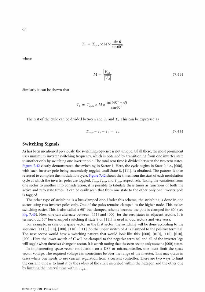
or
where
(7.43)
Similarly it can be shown that
The rest of the cycle can be divided between and T0 and T8. This can be expressed as
(7.44)
Switching Signals
As has been mentioned previously, the switching sequence is not unique. Of all these, the most prominentuses minimum inverter switching frequency, which is obtained by transitioning from one inverter stateto another only by switching one inverter pole. The total zero time is divided between the two zero states.Figure 7.42 clearly demonstrated the switching in Sector 1. Here, the cycle begins in State 0, i.e., [000],with each inverter pole being successively toggled until State 8, [111], is obtained. The pattern is thenreversed to complete the modulation cycle. Figure 7.42 shows the times from the start of each modulationcycle at which the inverter poles are toggled, TAon, TBon, and TCon, respectively. Taking the variations fromone sector to another into consideration, it is possible to tabulate these times as functions of both theactive and zero state times. It can be easily seen that from one state to the other only one inverter poleis toggled.
The other type of switching is a bus-clamped one. Under this scheme, the switching is done in onesector using two inverter poles only. One of the poles remains clamped to the higher node. This makesswitching easier. This is also called a 60° bus-clamped scheme because the pole is clamped for 60° (seeFig. 7.43). Now, one can alternate between [111] and [000] for the zero states in adjacent sectors. It istermed odd 60° bus-clamped switching if state 8 or [111] is used in odd sectors and vice versa.
For example, in case of a space vector in the first sector, the switching will be done according to thesequence [111], [110], [100], [110], [111]. So the upper switch of A is clamped to the positive terminal.The next sector would have a switching pattern that would look like this: [000], [010], [110], [010],[000]. Here the lower switch of C will be clamped to the negative terminal and all of the inverter legswill toggle when there is a change in sector. It is worth noting that the even sector only uses the [000] states.
In implementing space-vector modulation on a DSP or microcontroller, one must limit the spacevector voltage. The required voltage can sometimes be over the range of the inverter. This may occur incases where one needs to use current regulation from a current controller. There are two ways to limitthe current. One is to limit it by the radius of the circle inscribed within the hexagon and the other oneby limiting the interval time within Tcycle.
T2 Tcycle Mqsin
60°sin----------------××=
MVref
Vs2
------------=
T1 Tcycle M60° q–( )sin
60°sin------------------------------××=
Tcycle T1– T2– T0=
© 2002 by CRC Press LLC
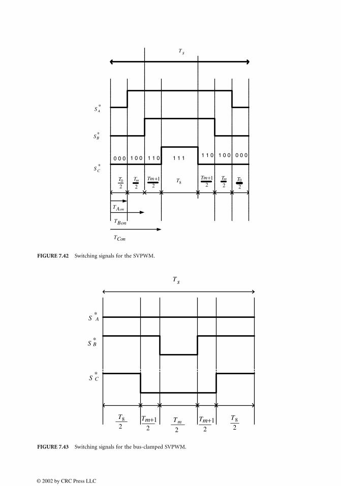
FIGURE 7.42 Switching signals for the SVPWM.
FIGURE 7.43 Switching signals for the bus-clamped SVPWM.
sT
S
AS∗
BS∗
CS∗
20T
2mT
21+Tm
8T20T
21+Tm
2mT
0 0 0 1 0 0 1 1 0 1 1 1 1 1 0 1 0 0 0 0 0
AonT
BonT
ConT
AS∗
BS∗
CS∗
sT
28T
2 2mT
28T
2
Tm+1Tm+1
© 2002 by CRC Press LLC
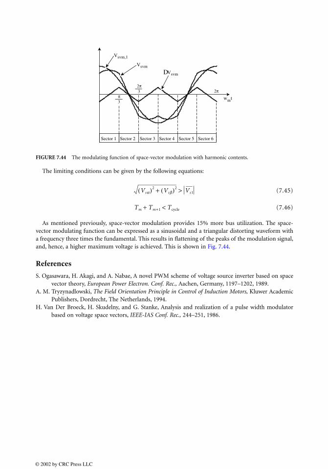
The limiting conditions can be given by the following equations:
(7.45)
(7.46)
As mentioned previously, space-vector modulation provides 15% more bus utilization. The space-vector modulating function can be expressed as a sinusoidal and a triangular distorting waveform witha frequency three times the fundamental. This results in flattening of the peaks of the modulation signal,and, hence, a higher maximum voltage is achieved. This is shown in Fig. 7.44.
References
S. Ogasawara, H. Akagi, and A. Nabae, A novel PWM scheme of voltage source inverter based on spacevector theory, European Power Electron. Conf. Rec., Aachen, Germany, 1197–1202, 1989.
A. M. Tryzynadlowski, The Field Orientation Principle in Control of Induction Motors, Kluwer AcademicPublishers, Dordrecht, The Netherlands, 1994.
H. Van Der Broeck, H. Skudelny, and G. Stanke, Analysis and realization of a pulse width modulatorbased on voltage space vectors, IEEE-IAS Conf. Rec., 244–251, 1986.
FIGURE 7.44 The modulating function of space-vector modulation with harmonic contents.
V
Sector 1 Sector 2 Sector 3 Sector 4 Sector 5 Sector 6
svm,1
Vsvm
VsvmD
π3
2π
w tm
32π
Vsa( )2 Vsb( )2+ Vs1>
Tm Tm+1+ Tcycle<
© 2002 by CRC Press LLC

8Sliding-Mode Control
of Switched-ModePower Supplies
8.1 Introduction8.2 Introduction to Sliding-Mode Control8.3 Basics of Sliding-Mode Theory
Existence Condition • Hitting Conditions •System Description in Sliding Mode: Equivalent Control •Stability
8.4 Application of Sliding-Mode Control to DC-DC Converters—Basic Principle
8.5 Sliding-Mode Control of Buck DC-DC ConvertersPhase-Plane Description • Selection of the Sliding Line • Existence Condition • Current Limitation
8.6 Extension to Boost and Buck–Boost DC-DC ConvertersStability Analysis
8.7 Extension to Cúk and SEPIC DC-DC ConvertersExistence Condition • Hitting Condition • Stability Condition
8.8 General-Purpose Sliding-Mode Control Implementation
8.9 Conclusions
Switch-mode power supplies represent a particular class of variable structure systems (VSS), and they cantake advantage of nonlinear control techniques developed for this class of system. Sliding-mode control,which is derived from variable structure system theory [1, 2], extends the properties of hysteresis controlto multivariable environments, resulting in stability even for large supply and load variations, gooddynamic response, and simple implementation.
Some basic principles of sliding-mode control are first reviewed. Then the application of the sliding-mode control technique to DC-DC converters is described. The application to buck converter is discussedin detail, and some guidelines for the extension of this control technique to boost, buck–boost, Cúk, andSEPIC converters are given. Finally, to overcome some inherent drawbacks of sliding-mode control,improvements like current limitation, constant switching frequency, and output voltage steady-state errorcancellation are described.
Giorgio Spiazzi University of Padova
Paolo MattavelliUniversity of Padova
© 2002 by CRC Press LLC

8.1 Introduction
Switch-mode power supplies (SMPS) are nonlinear and time-varying systems, and thus the design of ahigh-performance control is usually a challenging issue. In fact, control should ensure system stabilityin any operating condition and good static and dynamic performances in terms of rejection of inputvoltage disturbances and load changes. These characteristics, of course, should be maintained in spite oflarge input voltage, output current, and even parameter variations (robustness).
A classical control approach relies on the state space averaging method, which derives an equivalentmodel by circuit-averaging all the system variables in a switching period [3–5]. On the assumptions thatthe switching frequency is much greater than the natural frequency of system variables, low-frequencydynamics is preserved while high-frequency behavior is lost. From the average model, a suitable small-signal model is then derived by perturbation and linearization around a precise operating point. Finally,the small-signal model is used to derive all the necessary converter transfer functions to design a linearcontrol system by using classical control techniques. The design procedure is well known, but it is generallynot easy to account for the wide variation of system parameters, because of the strong dependence ofsmall-signal model parameters on the converter operating point. Multiloop control techniques, such ascurrent-mode control, have greatly improved power converter dynamic behavior, but the control designremains difficult especially for high-order topologies, such as those based on Cúk and SEPIC schemes.
The sliding-mode approach for variable structure systems (VSS) [1, 2] offers an alternative way to imple-ment a control action that exploits the inherent variable structure nature of SMPS. In particular, the converterswitches are driven as a function of the instantaneous values of the state variables to force the system trajectoryto stay on a suitable selected surface on the phase space. This control technique offers several advantages inSMPS applications [6–19]: stability even for large supply and load variations, robustness, good dynamicresponse, and simple implementation. Its capabilities emerge especially in application to high-orderconverters, yielding improved performances as compared with classical control techniques.
In this chapter, some basic principles of sliding-mode control are reviewed in a tutorial manner andits applications to DC-DC converters are investigated. The application to buck converters is first discussedin details, and then guidelines for the extension of this control technique to boost, buck–boost, Cúk,and SEPIC converters are given. Finally, improvements like current limitation, constant switching fre-quency, and output voltage steady-state error cancellation are discussed.
8.2 Introduction to Sliding-Mode Control
Sliding-mode control is a control technique based on VSS, defined as systems where the circuit topologyis intentionally changed, following certain rules, to improve the system behavior in terms of speed ofresponse, stability, and robustness. A VSS is based on a defined number of independent subtopologies,which are defined by the status of nonlinear elements (switches); the global dynamics of the systemis, however, substantially different from that of each single subtopology. The theory of VSS [1, 2] providesa systematic procedure for the analysis of these systems and for the selection and design of the controlrules. To introduce sliding-mode control, a simple example of a second-order system is analyzed. Twodifferent substructures are introduced and a combined action, which defines a sliding mode, is presented.The first substructure, which is referred as substructure I, is given by the following equations:
(8.1)
where the eigenvalues are complex with zero real part; thus, for this substructure the phase trajectoriesare circles, as shown in Fig. 8.1 and the system is marginally stable. The second substructure, which is
x1 x2=
x2 −K x1⋅=
© 2002 by CRC Press LLC

referred as substructure II, is given by
(8.2)
In this case the eigenvalues are real and with opposite sign; the corresponding phase trajectories areshown in Fig. 8.1 and the system is unstable. Only one phase trajectory, namely, x2 = −qx1 ,converges toward the origin, whereas all other trajectories are divergent.
Divide the phase-plane in two regions, as shown in Fig. 8.2; accordingly, at each region is associatedone of the two substructures as follows:
Region I: x1 · (x2 + cx1) < 0 ⇒ Substructure IRegion II: x1 · (x2 + cx1) > 0 ⇒ Substructure II
where c is lower than q. The switching boundaries are the x2 axis and the line x2 + cx1 = 0. The systemstructure changes whenever the system representative point (RP) enters a region defined by the switchingboundaries. The important property of the phase trajectories of both substructures is that, in the vicinityof the switching line x2 + cx1 = 0, they converge to the switching line. The immediate consequence ofthis property is that, once the RP hits the switching line, the control law ensures that the RP does notmove away from the switching line. Figure 8.2a shows a typical overall trajectory starting from an arbitraryinitial condition P0 (x10, x20): after the intervals corresponding to trajectories P0 – P1 (substructure I) andP1 – P2 (substructure II), the final state evolution lies on the switching line (in the hypothesis of idealinfinite frequency commutations between the two substructures).
This motion of the system RP along a trajectory, on which the structure of the system changes andwhich is not part of any of the substructure trajectories, is called the sliding mode, and the switching linex2 + cx1 = 0 is called the sliding line. When sliding mode exists, the resultant system performance iscompletely different from that dictated by any of the substructures of the VSS and can be, under particularconditions, made independent of the properties of the substructures employed and dependent only on
FIGURE 8.1 Phase-plane description corresponding to substructures I and II.
x1 x2=
x2 +K x1⋅=
q K=( )
© 2002 by CRC Press LLC

the control law (in this example the boundary x2 + cx1 = 0). In this case, for example, the dynamic is ofthe first order with a time constant equal to 1/c.
The independence of the closed-loop dynamics on the parameters of each substructure is not usuallytrue for more complex systems, but even in these cases it has been proved that the sliding-mode controlmaintains good robustness compared with other control techniques. For higher-order systems, the control
FIGURE 8.2 Sliding regime in VSS. (a) Ideal switching line; (b) switching line with hysteresis; (c) unstable slidingmode.
© 2002 by CRC Press LLC

rule can be written in the following way:
(8.3)
where N is the system order and xi are the state variables. Note that the choice of using a linear com-bination of state variable in Eq. (8.3) is only one possible solution, which results in a particularly simpleimplementation in SMPS applications.
When the switching boundary is not ideal, i.e., the commutation frequency between the two substruc-tures is finite, then the overall system trajectory is as shown in Fig. 8.2b. Of course, the width of thehysteresis around the switching line determines the switching frequency between the two substructures.
Following this simple example and looking at the Figs. 8.1 and 8.2, it is easy to understand that theconditions for realizing a sliding-mode control are:
• Existence condition: The trajectories of the two substructures are directed toward the sliding linewhen they are close to it.
• Hitting condition: Whatever the initial conditions, the system trajectories must reach the slidingline.
• Stability condition: The evolution of the system under sliding mode should be directed to a stablepoint. In Fig. 8.2b the system in sliding mode goes to the origin of the system, that is, a stablepoint. But if the sliding line were the following:
Region I: x1 · (x2 + cx1) < 0 ⇒ Substructure IRegion II: x1 · (x2 + cx1) > 0 ⇒ Substructure II
where c < 0, then the system trajectories would have been as shown in Fig. 8.2c. In this case, the resultingstate trajectory still follows the sliding line, but it goes to infinity and the system is therefore unstable.
The approach to more complex systems cannot be expressed only with graphical considerations, anda mathematical approach should be introduced, as reported below.
8.3 Basics of Sliding-Mode Theory
Consider the following general system with scalar control [1, 2]:
(8.4)
where x is a column vector and f is a function vector, both of dimension N, and u is an element that caninfluence the system motion (control input). Consider that the function vector f is discontinuous on asurface σ(x, t) = 0. Thus, one can write:
(8.5)
where the scalar discontinuous input u is given by
(8.6)
The system is in sliding mode if its representative point moves on the sliding surface σ(x, t) = 0.
s f x1,…, xN( ) cixi
i=1
N
∑ 0= = =
x f x, t, u( )=
f x, t, u( )f + x, t, u+( ) for s 0+→
f − x, t, u−( ) for s 0−→
=
uu+
for s x( ) 0>
u−for s x( ) 0<
=
© 2002 by CRC Press LLC

Existence Condition
For a sliding mode to exist, the phase trajectories of the two substructures corresponding to the two differentvalues of the vector function f must be directed toward the sliding surface σ(x, t) = 0 in a small regionclose to the surface itself. In other words, approaching the sliding surface from points where σ < 0, thecorresponding state velocity vector f
− must be directed toward the sliding surface, and the same must
happen when points above the surface (σ > 0) are considered, for which the corresponding state velocityvector is f
+. Indicating with subscript N the components of state velocity vectors f
+ and f
− orthogonal
to the sliding surface one can write:
(8.7)
where ∇σ is the gradient of surface σ. Since
(8.8)
the existence condition of the sliding mode becomes
(8.9)
When the inequality given by Eq. (8.9) holds in the entire state space and not only in an infinitesimalregion around the sliding surface, then this condition is also a sufficient condition that the system willreach the sliding surface.
Hitting Conditions
Let [x+] and [x
−] be the steady-state RPs corresponding to the inputs u
+ and u
− Eq. (8.6), respectively.
Then a simple sufficient condition, that will be used later in the application of the sliding mode controlto switch-mode power supplies, for reaching the sliding surface is given by:
(8.10)
In other words, if the steady-state point for one substructure belongs to the region of the phase spacereserved to the other substructure, then sooner or later the system RP will hit the sliding surface.
System Description in Sliding Mode: Equivalent Control
The next focus of interest in the analysis of VSS is the behavior of the system operating in sliding regime.Consider here a particular class of systems that are linear with the control input, i.e.,
(8.11)
where x ∈ ℜN, f and B ∈ ℑN
, u ∈ ℜ1.
fN+ 0<
s→o+
lim
fN− 0>
s→o−
lim
∇s f +⋅ 0<s →o
+lim
∇s f −⋅ 0>s→o
−lim
⇒
dsdt------ s∂
xi∂------
dxi
dt-------
i=1
N
∑ ∇s f⋅= =
dsdt------ 0<
s→o+
lim
dsdt------
s→o−
lim 0>s ds
dt------ 0<
s →olim⇒
x+[ ] s x( ) 0, x−[ ] s x( ) 0>∈<∈
x f x, t( ) B x, t( )u+=
© 2002 by CRC Press LLC
The scalar control input u is discontinuous on the sliding surface σ(x, t) = 0, as shown in Eq. (8.6),whereas f and B are continuous function vectors. Under sliding mode control, the system trajectoriesstay on the sliding surface, hence:
(8.12)
(8.13)
where G is a 1 by N matrix whose elements are the derivatives of the sliding surface with respect to thestate variables. By using Eqs. (8.11) and (8.13),
(8.14)
where the control input u was substituted by an equivalent control ueq that represents an equivalentcontinuous control input that maintains the system evolution on the sliding surface. On the assumptionthat [GB]
−1 exists, from Eq. (8.14) one can derive the expression for the equivalent control:
(8.15)
Finally, by substituting this expression into Eq. (8.11),
(8.16)
Equation (8.16) describes the system motion under sliding-mode control. It is important to note thatthe matrix is less than full rank. This is because, under sliding regime, the system motionis constrained to be on the sliding surface. As a consequence, the equivalent system described by Eq. (8.16)is of order N − 1. This equivalent control description of a VSS in sliding regime is valid, of course, alsofor multiple control inputs. For details, see Refs. 1 and 2.
Stability
Analyzing the system behavior in the phase-plane for the second-order system, it was found that thesystem stability is guaranteed if its trajectory, in sliding regime, is directed toward a stable operatingpoint. For higher-order systems, a direct view of the phase space is not feasible and one must provesystem stability through mathematical tools. First consider a simple linear system with scalar control inthe following canonical form:
(8.17)
and
(8.18)
The latter equation completely defines the system dynamic in sliding regime. Moreover, in this casethe system dynamic in sliding mode depends only on the sliding surface coefficients ci, leading to a systembehavior that is completely different from those given by the substructures defined by the two control
s x, t( ) 0= s x, t( )⇒ 0=
s˙ x, t( ) dsdt------ s∂
xi∂------
dxi
dt-------
i =1
N
∑ ∇s x⋅ Gx= = = =
Gx Gf x, t( ) GB x, t( )ueq+ 0= =
ueq − GB( )−1 Gf x, t( )=
x I B GB( )−1 G–[ ]f x, t( )=
I B GB( )−1 G–
xi xi+1 i 1, 2, …,N 1–= =
xN aNjxj bu+j=1
N
∑=
s x, t( ) cixi
i =1
N
∑ ci
di−1 x1
dti−1-------------
i =1
N
∑ 0= = =
© 2002 by CRC Press LLC
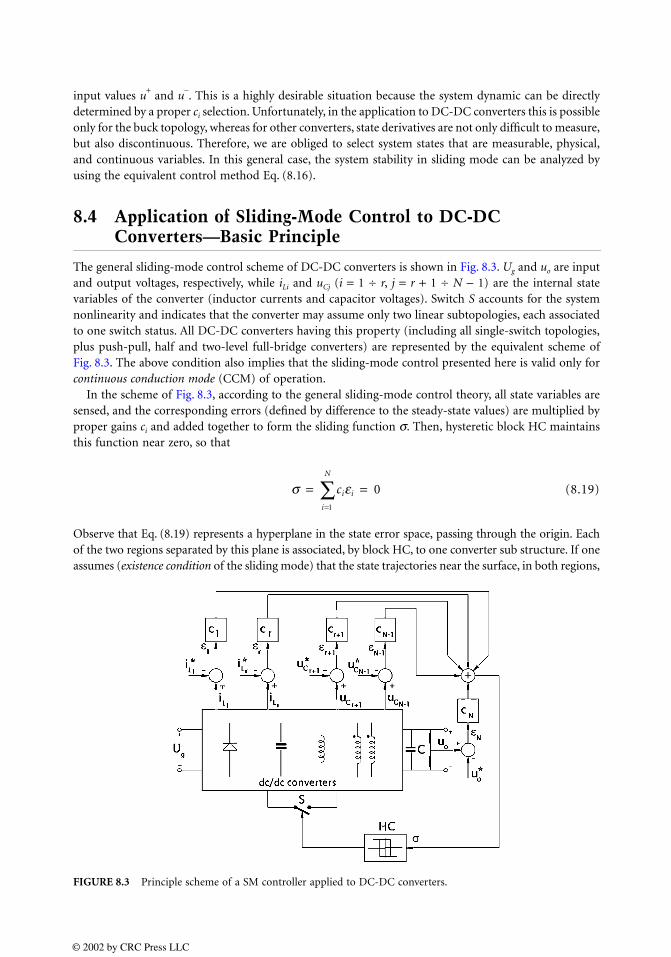
input values u+ and u
−. This is a highly desirable situation because the system dynamic can be directly
determined by a proper ci selection. Unfortunately, in the application to DC-DC converters this is possibleonly for the buck topology, whereas for other converters, state derivatives are not only difficult to measure,but also discontinuous. Therefore, we are obliged to select system states that are measurable, physical,and continuous variables. In this general case, the system stability in sliding mode can be analyzed byusing the equivalent control method Eq. (8.16).
8.4 Application of Sliding-Mode Control to DC-DC Converters—Basic Principle
The general sliding-mode control scheme of DC-DC converters is shown in Fig. 8.3. Ug and uo are inputand output voltages, respectively, while iLi and uCj (i = 1 ÷ r, j = r + 1 ÷ N − 1) are the internal statevariables of the converter (inductor currents and capacitor voltages). Switch S accounts for the systemnonlinearity and indicates that the converter may assume only two linear subtopologies, each associatedto one switch status. All DC-DC converters having this property (including all single-switch topologies,plus push-pull, half and two-level full-bridge converters) are represented by the equivalent scheme ofFig. 8.3. The above condition also implies that the sliding-mode control presented here is valid only forcontinuous conduction mode (CCM) of operation.
In the scheme of Fig. 8.3, according to the general sliding-mode control theory, all state variables aresensed, and the corresponding errors (defined by difference to the steady-state values) are multiplied byproper gains ci and added together to form the sliding function σ. Then, hysteretic block HC maintainsthis function near zero, so that
(8.19)
Observe that Eq. (8.19) represents a hyperplane in the state error space, passing through the origin. Eachof the two regions separated by this plane is associated, by block HC, to one converter sub structure. If oneassumes (existence condition of the sliding mode) that the state trajectories near the surface, in both regions,
FIGURE 8.3 Principle scheme of a SM controller applied to DC-DC converters.
s ciei
i=1
N
∑ 0= =
© 2002 by CRC Press LLC
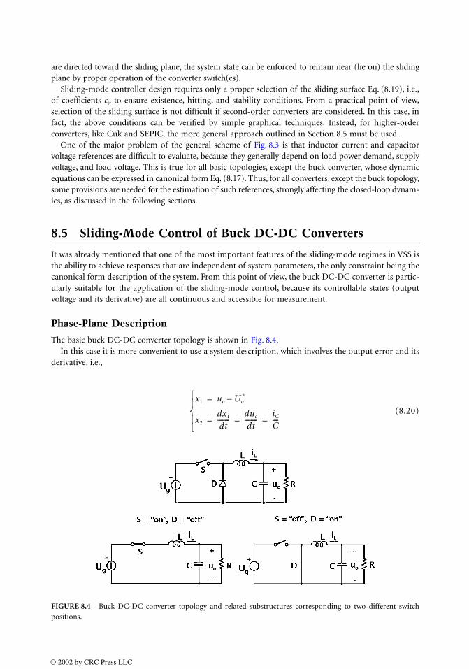
are directed toward the sliding plane, the system state can be enforced to remain near (lie on) the slidingplane by proper operation of the converter switch(es).
Sliding-mode controller design requires only a proper selection of the sliding surface Eq. (8.19), i.e.,of coefficients ci, to ensure existence, hitting, and stability conditions. From a practical point of view,selection of the sliding surface is not difficult if second-order converters are considered. In this case, infact, the above conditions can be verified by simple graphical techniques. Instead, for higher-orderconverters, like Cúk and SEPIC, the more general approach outlined in Section 8.5 must be used.
One of the major problem of the general scheme of Fig. 8.3 is that inductor current and capacitorvoltage references are difficult to evaluate, because they generally depend on load power demand, supplyvoltage, and load voltage. This is true for all basic topologies, except the buck converter, whose dynamicequations can be expressed in canonical form Eq. (8.17). Thus, for all converters, except the buck topology,some provisions are needed for the estimation of such references, strongly affecting the closed-loop dynam-ics, as discussed in the following sections.
8.5 Sliding-Mode Control of Buck DC-DC Converters
It was already mentioned that one of the most important features of the sliding-mode regimes in VSS isthe ability to achieve responses that are independent of system parameters, the only constraint being thecanonical form description of the system. From this point of view, the buck DC-DC converter is partic-ularly suitable for the application of the sliding-mode control, because its controllable states (outputvoltage and its derivative) are all continuous and accessible for measurement.
Phase-Plane Description
The basic buck DC-DC converter topology is shown in Fig. 8.4.In this case it is more convenient to use a system description, which involves the output error and its
derivative, i.e.,
(8.20)
FIGURE 8.4 Buck DC-DC converter topology and related substructures corresponding to two different switchpositions.
x1 uo Uo∗–=
x2
dx1
dt--------
duo
dt--------
iC
C----= = =
© 2002 by CRC Press LLC
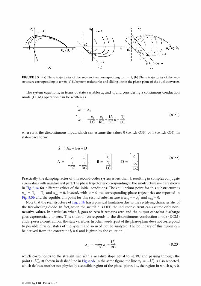
The system equations, in terms of state variables x1 and x2 and considering a continuous conductionmode (CCM) operation can be written as
(8.21)
where u is the discontinuous input, which can assume the values 0 (switch OFF) or 1 (switch ON). Instate-space form:
(8.22)
Practically, the damping factor of this second-order system is less than 1, resulting in complex conjugateeigenvalues with negative real part. The phase trajectories corresponding to the substructure u = 1 are shownin Fig. 8.5a for different values of the initial conditions. The equilibrium point for this substructure isxleq = Ug − and x2eq = 0. Instead, with u = 0 the corresponding phase trajectories are reported inFig. 8.5b and the equilibrium point for this second substructure is xleq = − and x2eq = 0.
Note that the real structure of Fig. 8.5b has a physical limitation due to the rectifying characteristic ofthe freewheeling diode. In fact, when the switch S is OFF, the inductor current can assume only non-negative values. In particular, when iL goes to zero it remains zero and the output capacitor dischargegoes exponentially to zero. This situation corresponds to the discontinuous-conduction mode (DCM)and it poses a constraint on the state variables. In other words, part of the phase-plane does not correspondto possible physical states of the system and so need not be analyzed. The boundary of this region canbe derived from the constraint iL = 0 and is given by the equation:
(8.23)
which corresponds to the straight line with a negative slope equal to −1/RC and passing through thepoint (− , 0) shown in dashed line in Fig. 8.5b. In the same figure, the line is also reported,which defines another not physically accessible region of the phase-plane, i.e., the region in which uo < 0.
FIGURE 8.5 (a) Phase trajectories of the substructure corresponding to u = 1; (b) Phase trajectories of the sub-structure corresponding to u = 0; (c) Subsystem trajectories and sliding line in the phase-plane of the buck converter.
x1 x2=
x2 −x1
LC-------
x2
RC-------
Ug
LC------- u
Uo∗
LC-------–+–=
x Ax Bu D+ +=
A0 1
− 1LC------- − 1
RC-------
, B0
Ug
LC-------
, D0
−Uo
∗
LC-------
===
Uo∗
Uo∗
x2 − 1RC------- x1
Uo∗
RC-------–=
Uo∗ x1 Uo
∗–=
© 2002 by CRC Press LLC
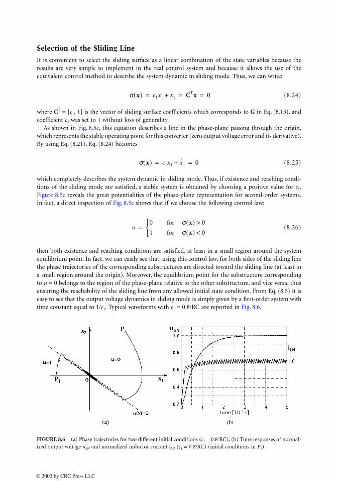
Selection of the Sliding Line
It is convenient to select the sliding surface as a linear combination of the state variables because theresults are very simple to implement in the real control system and because it allows the use of theequivalent control method to describe the system dynamic in sliding mode. Thus, we can write:
(8.24)
where CT = [c1, 1] is the vector of sliding surface coefficients which corresponds to G in Eq. (8.13), and
coefficient c2 was set to 1 without loss of generality.As shown in Fig. 8.5c, this equation describes a line in the phase-plane passing through the origin,
which represents the stable operating point for this converter (zero output voltage error and its derivative).By using Eq. (8.21), Eq. (8.24) becomes
(8.25)
which completely describes the system dynamic in sliding mode. Thus, if existence and reaching condi-tions of the sliding mode are satisfied, a stable system is obtained by choosing a positive value for c1.Figure 8.5c reveals the great potentialities of the phase-plane representation for second-order systems.In fact, a direct inspection of Fig. 8.5c shows that if we choose the following control law:
(8.26)
then both existence and reaching conditions are satisfied, at least in a small region around the systemequilibrium point. In fact, we can easily see that, using this control law, for both sides of the sliding linethe phase trajectories of the corresponding substructures are directed toward the sliding line (at least ina small region around the origin). Moreover, the equilibrium point for the substructure correspondingto u = 0 belongs to the region of the phase-plane relative to the other substructure, and vice versa, thusensuring the reachability of the sliding line from any allowed initial state condition. From Eq. (8.5) it iseasy to see that the output voltage dynamics in sliding mode is simply given by a first-order system withtime constant equal to 1/c1. Typical waveforms with c1 = 0.8/RC are reported in Fig. 8.6.
FIGURE 8.6 (a) Phase trajectories for two different initial conditions (c1 = 0.8/RC); (b) Time responses of normal-ized output voltage uoN and normalized inductor current iLN (c1 = 0.8/RC) (initial conditions in P1).
s x( ) c1x1 x2+ CTx 0= = =
s x( ) c1x1 x1+ 0= =
u0 for s x( ) 0>1 for s x( ) 0<
=
© 2002 by CRC Press LLC
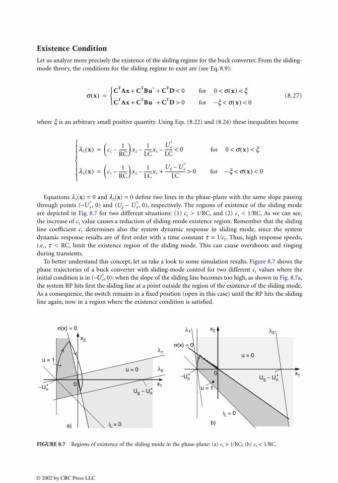
Existence Condition
Let us analyze more precisely the existence of the sliding regime for the buck converter. From the sliding-mode theory, the conditions for the sliding regime to exist are (see Eq. 8.9):
(8.27)
where ξ is an arbitrary small positive quantity. Using Eqs. (8.22) and (8.24) these inequalities become
Equations λ1(x) = 0 and λ2(x) = 0 define two lines in the phase-plane with the same slope passingthrough points (− , 0) and (Ug − , 0), respectively. The regions of existence of the sliding modeare depicted in Fig. 8.7 for two different situations: (1) c1 > 1/RC, and (2) c1 < 1/RC. As we can see,the increase of c1 value causes a reduction of sliding-mode existence region. Remember that the slidingline coefficient c1 determines also the system dynamic response in sliding mode, since the systemdynamic response results are of first order with a time constant τ = 1/c1. Thus, high response speeds,i.e., τ < RC, limit the existence region of the sliding mode. This can cause overshoots and ringingduring transients.
To better understand this concept, let us take a look to some simulation results. Figure 8.7 shows thephase trajectories of a buck converter with sliding-mode control for two different c1 values where theinitial condition is in (− , 0): when the slope of the sliding line becomes too high, as shown in Fig. 8.7a,the system RP hits first the sliding line at a point outside the region of the existence of the sliding mode.As a consequence, the switch remains in a fixed position (open in this case) until the RP hits the slidingline again, now in a region where the existence condition is satisfied.
FIGURE 8.7 Regions of existence of the sliding mode in the phase-plane: (a) c1 > 1/RC; (b) c1 < 1/RC.
s˙ x( )CTAx CTBu+ CTD 0<++ for 0 s x( ) x< <
CTAx CTBu− CTD 0>++ for −x s x( )< 0<
=
l1 x( ) c11
RC-------–
x21
LC-------x1
Uo∗
LC------- 0 for 0 s x( ) x< <<––=
l2 x( ) c11
RC-------–
x21
LC-------x1
Ug Uo∗–
LC------------------ 0 for −x s x( )< 0<>+–=
Uo∗ Uo
∗
Uo∗
σ(x) = 0
Ug Uo*Uo*
u = 0
u = 1
iL = 0
λ1
λ2
x2
x1
a)
0u = 1
b)
0Ug Uo*Uo*
u = 0
σ(x) = 0
iL = 0
λ1 λ2x2
x1
© 2002 by CRC Press LLC
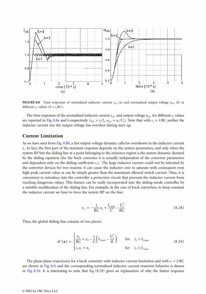
The time responses of the normalized inductor current iLN and output voltage uoN for different c1 valuesare reported in Fig. 8.8a and b respectively (iLN = iL/Io, uoN = uo/Uo). Note that with c1 = 1/RC neither theinductor current nor the output voltage has overshot during start-up.
Current Limitation
As we have seen from Fig. 8.8b, a fast output voltage dynamic calls for overshoots in the inductor currentiL. In fact, the first part of the transient response depends on the system parameters, and only when thesystem RP hits the sliding line at a point belonging to the existence region is the system dynamic dictatedby the sliding equation (for the buck converter it is actually independent of the converter parametersand dependent only on the sliding coefficient c1). The large inductor current could not be tolerated bythe converter devices for two reasons: it can cause the inductor core to saturate with consequent evenhigh-peak current value or can be simply greater than the maximum allowed switch current. Thus, it isconvenient to introduce into the controller a protection circuit that prevents the inductor current fromreaching dangerous values. This feature can be easily incorporated into the sliding-mode controller bya suitable modification of the sliding line. For example, in the case of buck converters, to keep constantthe inductor current we have to force the system RP on the line:
(8.28)
Thus, the global sliding line consists of two pieces:
(8.29)
The phase plane trajectories for a buck converter with inductor current limitation and with c1 = 2/RCare shown in Fig. 8.9, and the corresponding normalized inductor current transient behavior is shownin Fig. 8.10. It is interesting to note that Eq. (8.29) gives an explanation of why the fastest response
FIGURE 8.8 Time responses of normalized inductor current iLN (a) and normalized output voltage uoN (b) atdifferent c1 values (k = c1RC).
x2 − 1RC------- x1
ILmax
C----------
Uo∗
RC-------–+=
s ′ x( )x1
RC------- x2
1C--- ILmax
Uo∗
R------–
for iL ILmax>–+
c1x1 x2 for iL ILmax<+
=
© 2002 by CRC Press LLC
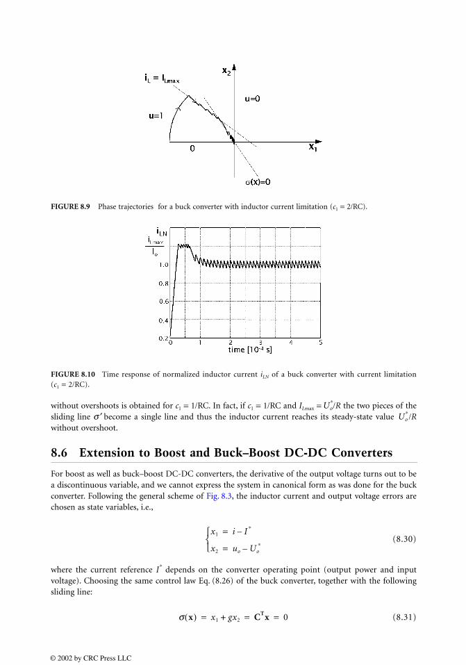
without overshoots is obtained for c1 = 1/RC. In fact, if c1 = 1/RC and ILmax = /R the two pieces of thesliding line σ ′ become a single line and thus the inductor current reaches its steady-state value /Rwithout overshoot.
8.6 Extension to Boost and Buck–Boost DC-DC Converters
For boost as well as buck–boost DC-DC converters, the derivative of the output voltage turns out to bea discontinuous variable, and we cannot express the system in canonical form as was done for the buckconverter. Following the general scheme of Fig. 8.3, the inductor current and output voltage errors arechosen as state variables, i.e.,
(8.30)
where the current reference I∗ depends on the converter operating point (output power and input
voltage). Choosing the same control law Eq. (8.26) of the buck converter, together with the followingsliding line:
(8.31)
FIGURE 8.9 Phase trajectories for a buck converter with inductor current limitation (c1 = 2/RC).
FIGURE 8.10 Time response of normalized inductor current iLN of a buck converter with current limitation(c1 = 2/RC).
Uo∗
Uo∗
x1 i I ∗–=
x2 uo Uo∗–=
s x( ) x1 gx2+ CTx 0= = =
© 2002 by CRC Press LLC
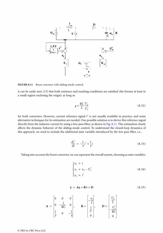
it can be easily seen [13] that both existence and reaching conditions are satisfied (the former at least ina small region enclosing the origin) as long as
(8.32)
for both converters. However, current reference signal I∗ is not usually available in practice, and some
alternative techniques for its estimation are needed. One possible solution is to derive this reference signaldirectly from the inductor current by using a low-pass filter, as shown in Fig. 8.11. This estimation clearlyaffects the dynamic behavior of the sliding-mode control. To understand the closed-loop dynamics ofthis approach, we need to include the additional state variable introduced by the low-pass filter, i.e.,
(8.33)
Taking into account the boost converter, we can represent the overall system, choosing as state variables:
(8.34)
(8.35)
FIGURE 8.11 Boost converter with sliding-mode control.
gRCL
-------Ug
Uo∗------<
di∗
dt------- −1
t-- i∗ 1
t-- i+=
x1 i=
x2 uo Uo∗–=
x3 i∗=
x Ax Bu D+ +=
A
0 0 0
0 − 1RC------- 0
1t-- 0 −1
t--
, B
−uo
L-----
iC---
0
, D
Ug
L------
−Uo
∗
RC-------
0
===
© 2002 by CRC Press LLC

The sliding line becomes a sliding surface in the phase space:
(8.36)
where CT = [1, g, −1] is the vector of the sliding surface coefficients and x1 − x3 represents now the
inductor current error. Fortunately, the existence conditions analysis for the system Eq. (8.35) leads tothe same constraint (8.32), which can be derived without accounting for the low-pass filter dynamic[13]. However, unlike the buck converter, Eq. (8.32) does not directly give information on the systemstability and on the possible values of filter time constant τ.
Stability Analysis
In the following, a procedure similar to the equivalent control method is used to derive a suitable smallsignal model for the system Eq. (8.35) in sliding mode. The starting point is the small-signal state spaceaveraged model of the boost converter [3]:
(8.37)
where and D′ = 1 − D. In Eq. (8.37), the dynamic equation of the low-pass filter Eq. (8.33) was added to the original boost equations. From the sliding surface definition wecan write:
(8.38)
where CT = [1, g, −1] and the steady-state values X of the state variables coincide with the corresponding
reference values X∗. Now, if the system is in sliding regime, we can write
(8.39)
From Eqs. (8.37) and (8.39) we can derive an expression for the duty-cycle perturbation as a functionof the state variables and the input, which, substituted into Eq. (8.37), yields:
(8.40)
In Eq. (8.40), which represents a third-order system, one equation (for example, the last one correspond-ing to the variable x3) is redundant and can be eliminated by using the equation σ = 0. The result is the
s x( ) x1 gx2 x3–+ CTx 0= = =
x Ax Bug Cd+ +=
A
0 −D′L------ 0
D′C------ − 1
RC------- 0
1t-- 0 −1
t--
, B
1L---
0
0
, DUg
D′------
1L---
− 1D′RC--------------
0
===
x x1, x2, x3[ ]Ti, uo, i
∗[ ]T
= =
s x( ) i i∗–( ) g uo Uo∗–( )+ i i
∗guo+– CTx= = =
s x( ) 0 s˙ x( )⇒ CTx 0= = =
x A′ x B′ ug+=
© 2002 by CRC Press LLC
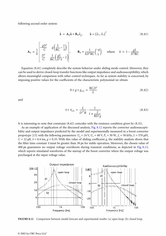
following second-order system:
(8.41)
Equation (8.41) completely describe the system behavior under sliding mode control. Moreover, theycan be used to derive closed-loop transfer functions like output impedance and audiosusceptibility, whichallows meaningful comparison with other control techniques. As far as system stability is concerned, byimposing positive values for the coefficients of the characteristic polynomial we obtain
(8.42)
and
(8.43)
It is interesting to note that constraint (8.42) coincides with the existence condition given by (8.32). As an example of application of the discussed analysis, Fig. 8.12 reports the converter audiosuscepti-
bility and output impedance predicted by the model and experimentally measured in a boost converterpropotype [13] with the following parameters: Ug = 24 V, Uo = 48 V, Po = 50 W, fs = 50 kHz, L = 570 µH,C = 22 µF, τ = 0.4 ms, g = 0.35. With this value of sliding coefficient g, the stability analysis shows thatthe filter time constant τ must be greater than 38 µs for stable operation. Moreover, the chosen value of400 µs guarantees no output voltage overshoots during transient conditions, as depicted in Fig. 8.13,which reports simulated waveforms of the startup of the boost converter where the output voltage wasprecharged at the input voltage value.
FIGURE 8.12 Comparison between model forecast and experimental results: (a) open loop; (b) closed loop.
x ATx BTug, x x1, x2[ ]T=+=
AT1k--
−gD′C
-------- g2
RC------- 1
t--–
D′C------ 1
RC------- gL
D′t--------- 2–
, BT
1kD′RC-----------------
g–
1 where k= 1
gLD′RC--------------–= =
0 g g< < critRCD′
L--------------=
t tcrit> L
D′2R------------ 1
12
RD′g------------+
----------------------⋅=
© 2002 by CRC Press LLC
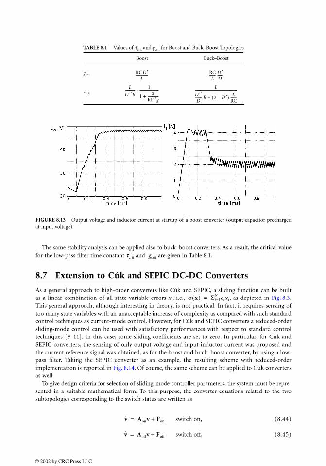
The same stability analysis can be applied also to buck–boost converters. As a result, the critical valuefor the low-pass filter time constant τcrit and gcrit are given in Table 8.1.
8.7 Extension to Cúk and SEPIC DC-DC Converters
As a general approach to high-order converters like Cúk and SEPIC, a sliding function can be builtas a linear combination of all state variable errors xi, i.e., , as depicted in Fig. 8.3.This general approach, although interesting in theory, is not practical. In fact, it requires sensing oftoo many state variables with an unacceptable increase of complexity as compared with such standardcontrol techniques as current-mode control. However, for Cúk and SEPIC converters a reduced-ordersliding-mode control can be used with satisfactory performances with respect to standard controltechniques [9–11]. In this case, some sliding coefficients are set to zero. In particular, for Cúk andSEPIC converters, the sensing of only output voltage and input inductor current was proposed andthe current reference signal was obtained, as for the boost and buck–boost converter, by using a low-pass filter. Taking the SEPIC converter as an example, the resulting scheme with reduced-orderimplementation is reported in Fig. 8.14. Of course, the same scheme can be applied to Cúk convertersas well.
To give design criteria for selection of sliding-mode controller parameters, the system must be repre-sented in a suitable mathematical form. To this purpose, the converter equations related to the twosubtopologies corresponding to the switch status are written as
(8.44)
(8.45)
TABLE 8.1 Values of τcrit and gcrit for Boost and Buck–Boost Topologies
Boost Buck–Boost
gcrit
τcrit
FIGURE 8.13 Output voltage and inductor current at startup of a boost converter (output capacitor prechargedat input voltage).
RCD ′L
-------------- RCL
------- D ′D------
L
D ′2R------------ 1
12
RD ′g-------------+
----------------------⋅ L
D ′2
D-------- R 2 D ′–( ) L
RC-------+
-------------------------------------------------
s x( ) Σi=1N cixi=
v Aonv Fon switch on,+=
v Aoffv Foff switch off,+=
© 2002 by CRC Press LLC

where v = [i1, i2, u1, u2]T is the state variable vector. These equations are combined in the following form
(VSS)
(8.46)
where u is the discontinuous variable corresponding to the switch status and matrices A, B, F are given by
A = Aoff, F = Foff, (8.47)
B = (Aon − Aoff )v + (Fon − Foff ) (8.48)
It is convenient to write the system Eq. (8.47) in terms of state variables error xi, where x = v − V∗,
being V∗ = [ , , , ]
T the vector of state variable references. Accordingly, system equations become
(8.49)
where G = AV∗ + F.
Existence Condition
Assuming that the switch is kept on when σ is negative and off when σ is positive, we may express theexistence condition in the form (see Eq. 8.9):
(8.50)
where ξ is an arbitrary small positive quantity. Inequalities (8.50) are useful only if state variable errorsxi are bounded; otherwise, (8.50) must be analyzed under small-signal assumption. In this latter case,satisfying (8.50) means enforcing the existence condition in a small volume around the operating point,and this is equivalent to ensuring the stability condition as demonstrated in Ref. 13.
Hitting Condition
If sliding mode exists, a sufficient hitting condition is
(8.51)
FIGURE 8.14 SEPIC converter with sliding-mode control.
u2
+
++
+
+ −
+
−
−−
u1i1
C1 C2
D
S RL2L1
Cu
Ug
iCH1
xi xu
U*2I*1
L.P.F
1:n
v Av Bu F,+ +=
I1∗ I2
∗ U1∗
U2∗
x Ax Bu G,+ +=
∂s∂t------ CTAx CTG 0 0 s x<< <+=
∂s∂t------ CTAx CTB CTG+ 0 −x> s 0,<<+=
CTA4 0≤
© 2002 by CRC Press LLC
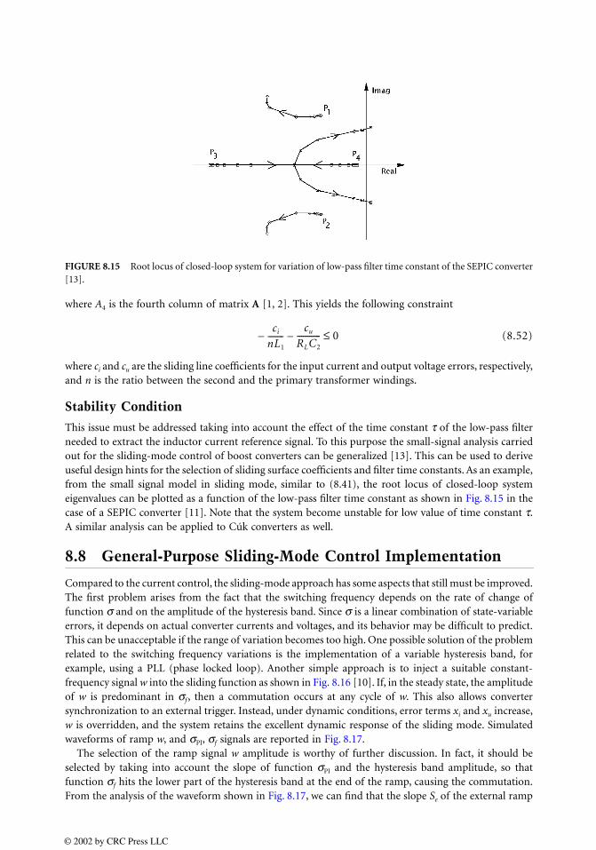
where A4 is the fourth column of matrix A [1, 2]. This yields the following constraint
(8.52)
where ci and cu are the sliding line coefficients for the input current and output voltage errors, respectively,and n is the ratio between the second and the primary transformer windings.
Stability Condition
This issue must be addressed taking into account the effect of the time constant τ of the low-pass filterneeded to extract the inductor current reference signal. To this purpose the small-signal analysis carriedout for the sliding-mode control of boost converters can be generalized [13]. This can be used to deriveuseful design hints for the selection of sliding surface coefficients and filter time constants. As an example,from the small signal model in sliding mode, similar to (8.41), the root locus of closed-loop systemeigenvalues can be plotted as a function of the low-pass filter time constant as shown in Fig. 8.15 in thecase of a SEPIC converter [11]. Note that the system become unstable for low value of time constant τ.A similar analysis can be applied to Cúk converters as well.
8.8 General-Purpose Sliding-Mode Control Implementation
Compared to the current control, the sliding-mode approach has some aspects that still must be improved.The first problem arises from the fact that the switching frequency depends on the rate of change offunction σ and on the amplitude of the hysteresis band. Since σ is a linear combination of state-variableerrors, it depends on actual converter currents and voltages, and its behavior may be difficult to predict.This can be unacceptable if the range of variation becomes too high. One possible solution of the problemrelated to the switching frequency variations is the implementation of a variable hysteresis band, forexample, using a PLL (phase locked loop). Another simple approach is to inject a suitable constant-frequency signal w into the sliding function as shown in Fig. 8.16 [10]. If, in the steady state, the amplitudeof w is predominant in σf , then a commutation occurs at any cycle of w. This also allows convertersynchronization to an external trigger. Instead, under dynamic conditions, error terms xi and xu increase,w is overridden, and the system retains the excellent dynamic response of the sliding mode. Simulatedwaveforms of ramp w, and σPI, σf signals are reported in Fig. 8.17.
The selection of the ramp signal w amplitude is worthy of further discussion. In fact, it should beselected by taking into account the slope of function σPI and the hysteresis band amplitude, so thatfunction σf hits the lower part of the hysteresis band at the end of the ramp, causing the commutation.From the analysis of the waveform shown in Fig. 8.17, we can find that the slope Se of the external ramp
FIGURE 8.15 Root locus of closed-loop system for variation of low-pass filter time constant of the SEPIC converter[13].
ci
nL1
--------–cu
RLC2
------------ 0≤–
© 2002 by CRC Press LLC
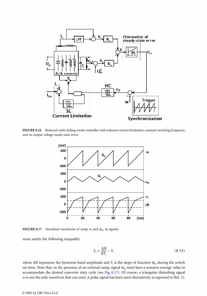
must satisfy the following inequality
(8.53)
where ∆B represents the hysteresis band amplitude and Sr is the slope of function σPI during the switchon-time. Note that, in the presence of an external ramp, signal σPI must have a nonzero average value toaccommodate the desired converter duty cycle (see Fig. 8.17). Of course, a triangular disturbing signalw is not the only waveform that can used. A pulse signal has been used alternatively as reported in Ref. 12.
FIGURE 8.16 Reduced-order sliding-mode controller with inductor current limitation, constant switching frequency,and no output voltage steady-state error.
FIGURE 8.17 Simulated waveforms of ramp w, and σPI, σf signals.
wSe
Sr
σf
∆B
σPI
0 20 40 60 80 [ms]
200
-200
0
[mV]
200
-200
0
200
-200
0
Se∆BdTs
-------- Sr–>
© 2002 by CRC Press LLC
The second problem derives from a possible steady state error on the output voltage. In fact, when theinductor current reference is evaluated using a low-pass filter, then the current error leads naturally tozero average value in steady state. Thus, if the sliding function, due to the hysteretic control or due tothe added ramp signal w, has nonzero average value, a steady-state output voltage error necessarilyappears. This problem can be solved by introducing a PI action on sliding function to eliminate its DCvalue (see Fig. 8.16). In practice, the integral action of this regulator is enabled only when the system ison the sliding surface; in this way, the system behavior during large transients, when σ can have valuesfar from zero, is not affected, thus maintaining the large-signal dynamic characteristics of sliding-modecontrol. A general-purpose sliding-mode controller scheme that includes the aforementioned improve-ments, together with reduced-order implementation in the case of Cúk and SEPIC converters and apossible implementation of current limitation by means of another hysteretic comparator and an ANDport, is reported in Fig. 8.16. Experimental results of this scheme are reported in Refs. 10 and 11.
8.9 Conclusions
Control techniques of VSS find a natural application to SMPS, since they inherently show variablestructure properties as a result of the conversion process and switch modulation. Thus, the sliding-modecontrol represents a powerful tool to enhance performance of power converters. Sliding-mode control isable to ensure system stability even for large supply and load variations, good dynamic response, andsimple implementation, even for high-order converters. These features make this control technique avalid alternative to standard control approaches.
The application of the sliding-mode control technique to DC-DC converters is the focus of this chapter.The application to buck converters is discussed in detail, whereas for the extension of this control techniqueto boost, buck–boost, Cúk, and SEPIC converters only some design guidelines are given. Finally, suchimprovements as current limitation, constant switching frequency, and output voltage steady-state errorcancellation are outlined. This control approach can also be effectively used in other applications, notdiscussed here, such as inverters [14, 18], power factor controllers [16], and AC power supplies [17].
References
1. V. I. Utkin, Sliding Modes and Their Application in Variable Structure Systems, MIR Publishers,Moscow, 1978.
2. U. Itkis, Control Systems of Variable Structure, John Wiley & Sons, New York, 1976.3. R. D. Middlebrook and S. Cuk, Advances in Switched-Mode Power Conversion, Vol. I and II, TESLAco,
Pasadena, CA, 1983, 73–89.4. R. Redl and N. Sokal, Current-mode control, five different types, used with the three basic classes
of power converters: small-signal AC and large-signal DC characterization, stability requirements,and implementation of practical circuits, in IEEE-PESC, 1985, 771–785.
5. J. G. Kassakian, M. F. Schlecht, and G. C. Verghese, Principles of Power Electronics, Addison-Wesley,Reading, MA, 1991.
6. R. Venkataramanan, A. Sabanovic, and S. Cúk, Sliding-mode control of DC-to-DC converters, inIECON Conf. Proc., 1985, 251–258.
7. B. Nicolas, M. Fadel, and Y. Chéron, Robust control of switched power converters via sliding mode,ETEP, 6(6), 413–418, 1996.
8. B. Nicolas, M. Fadel, and Y. Chéron, Sliding mode control of DC-to-DC converters with input filterbased on Lyapunov-function approach, in EPE Conf. Proc., 1995, 1.338–1.343.
9. L. Malesani, L. Rossetto, G. Spiazzi, and P. Tenti, Performance optimization of Cúk converters bysliding-mode control, IEEE Trans. Power Electron., 10(3), 302–309, 1995.
10. P. Mattavelli, L. Rossetto, G. Spiazzi, and P. Tenti, General-purpose sliding-mode controller forDC/DC converter applications, in Proc. of IEEE Power Electronics Specialists Conf. (PESC), Seattle,June 1993, 609–615.
© 2002 by CRC Press LLC

11. P. Mattavelli, L. Rossetto, G. Spiazzi, and P. Tenti, Sliding mode control of SEPIC converters, in Proc.of European Space Power Conf. (ESPC), Graz, August 1993, 173–178.
12. J. Fernando Silva and Sonia S. Paulo, Fixed frequency sliding mode modulator for current modePWM inverters, in Power Electronics Specialists Conf. Proc. (PESC), 1993, 623–629.
13. P. Mattavelli, L. Rossetto, and G. Spiazzi, Small-signal analysis of DC-DC converters with slidingmode control, IEEE Trans. Power Electron., 12(1), 79–86, 1997.
14. N. Sabanovic, A. Sabanovic, and K. Ohnishi, Sliding mode control of three-phase switching converters,in Proc. of Int. Conf. on Industrial Electronics, Control and Instrumentation (IECON), San Diego, 1992,319–325.
15. N. Sabanovic-Behlilovic, A. Sabanovic, and T. Ninomiya, PWM in three-phase switching converters-sliding mode solution, in Power Electronics Specialists Conference, PESC ’94 Record, 25th Annual IEEE,Vol. 1, 1994, 560–565.
16. L. Rossetto, G. Spiazzi, B. Fabiano, and C. Licitra, Fast-response high-quality rectifier with slidingmode control, IEEE Trans. Power Electron., 9(2), 146–152, 1994.
17. L. Malesani, L. Rossetto, G. Spiazzi, and A. Zuccato, An AC power supply with sliding-mode control,IEEE Ind. Appl. Mag., 2(5), 32–38, 1996.
18. H. Pinheiro, A. S. Martins, and J. R. Pinheiro, A sliding mode controller in single phase voltagesource inverters, in IEEE IECON ’94, 1994, 394–398.
19. H. Sira-Ramirez and M. Rios-Bolivar, Sliding mode control of DC-to-DC power converters viaextended linearization circuits and systems I: fundamental theory and applications, IEEE Transactionson Circuits and Systems 41(10), 652–661, 1994.
© 2002 by CRC Press LLC

IIIApplications and Systems Considerations
9 DC Motor Drives Ralph StausDC Motor Basics • DC Speed Control • DC Drive Basics • Transistor PWM DCDrives • SCR DC Drives
10 AC Machines Controlled as DC Machines (Brushless DCMachines/Electronics) Hamid A. Toliyat, Tilak GopalarathnamIntroduction • Machine Construction • Motor Characteristics • PowerElectronic Converter • Position Sensing • Pulsating Torque Components •Torque-Speed Characteristics • Applications
11 Control of Induction Machine Drives Daniel Logue, Philip T. KreinIntroduction • Scalar Induction Machine Control • Vector Control of InductionMachines • Summary
12 Permanent Magnet Synchronous Machine Drives Patrick L. ChapmanIntroduction • Construction of PMSM Drive Systems • Simulationand Model • Controlling the PMSM • Advanced Topics in PMSM Drives
13 Switched Reluctance Machines Iqbal HusainIntroduction • SRM Configuration • Basic Principle of Operation • Design • ConverterTopologies • Control Strategies • Sensorless Control • Applications
14 Step Motor Drives Ronald H. BrownIntroduction • Types and Operation of Step Motors • Step Motor Models • Controlof Step Motors
15 Servo Drives Sándor HalászDC Drives • Induction Motor Drives
16 Uninterruptible Power Supplies Laura Steffek, John Hecklesmiller,Dave Layden, Brian YoungUPS Functions • Static UPS Topologies • Rotary UPSs • Alternate AC and DC Sources
17 Power Quality and Utility Interface Issues Wayne Galli, Timothy L. Skvarenina,Badrul H. Chowdhury, Hirofumi Akagi, Rajapandian Ayyanar, Amit Kumar JainOverview • Power Quality Considerations • Passive Harmonic Filters • Active Filtersfor Power Conditioning • Unity Power Factor Rectification
18 Photovoltaic Cells and Systems Roger MessengerIntroduction • Solar Cell Fundamentals • Utility Interactive PV Applications •Stand-Alone PV Systems
© 2002 by CRC Press LLC

19 Flexible, Reliable, and Intelligent Electrical Energy Delivery SystemsAlexander Domijan, Jr., Zhidong SongIntroduction • The Concept of FRIENDS • Development of FRIENDS • The AdvancedPower Electronic Technologies within QCCs • Significance of FRIENDS • Realizationof FRIENDS • Conclusions
20 Unified Power Flow Controllers Ali Feliachi, Azra Hasanovic, Karl SchoderIntroduction • Power Flow on a Transmission Line • UPFC Description and Operation •UPFC Modeling • Control Design • Case Study • Conclusion
21 More-Electric Vehicles Ali Emadi, Mehrdad EhsaniAircraft • Terrestrial Vehicles
22 Principles of Magnetics Roman StemprokIntroduction • Nature of a Magnetic Field • Electromagnetism • MagneticFlux Density • Magnetic Circuits • Magnetic Field Intensity • Maxwell’sEquations • Inductance • Practical Considerations
23 Computer Simulation of Power Electronics Michael GiesselmannIntroduction • Code Qualification and Model Validation • Basic Concepts—Simulationof a Buck Converter • Advanced Techniques—Simulation of a Full-Bridge (H-Bridge)Converter • Conclusions
© 2002 by CRC Press LLC

9DC Motor Drives
9.1 DC Motor Basics9.2 DC Speed Control9.3 DC Drive Basics9.4 Transistor PWM DC Drives9.5 SCR DC Drives
9.1 DC Motor Basics
The DC motor consists of two basic parts: a stationary magnetic field and a current-carrying coil on thearmature. The force produced by the interaction of these two components produces a torque that causesthe armature to rotate. The stationary magnetic field is produced by a permanent magnet for many smallDC motors. Large and extended speed range motors use an electromagnet to produce the stationary fieldpermitting the drive to control the field strength. The armature coils consists of a series of individualcoils connected to the DC power source through a commutator and brushes. As the armature rotates,the commutator switches successive coils into the circuit to keep the armature coil and magnetic polesin the same relative position.
The field flux φ (Eq. 9.1) is a function of the field current If and a proportionality constant kf. Thetorque T produced (Eq. 9.2) is related to the field flux and armature current ia by the proportionalityconstant kt. The speed of a DC motor is controlled by the torque produced by the motor and the torquerequired by the load. When the motor torque exceeds the load requirement, the rotational speed of themotor increases.
(9.1)
(9.2)
The armature current is in response to the applied voltage V (Eq. 9.3) and is opposed by a counter-voltage (ea) produced by the armature coil rotating through the stationary magnetic field and the armatureresistance (Ra). The countervoltage (Eq. 9.4) produced by the armature is proportional to the strengthof the stationary field and the rotational speed (S). Below the rated base speed of the motor the currentin the stationary magnetic field coil is kept constant. Therefore, at values below base speed the DC motorspeed is a function of the applied voltage and resistive loss in the armature.
(9.3)
(9.4)
f kfIf=
T ktfia=
V ea Raia+=
ea keφS=
Ralph StausPennsylvania State University
© 2002 by CRC Press LLC
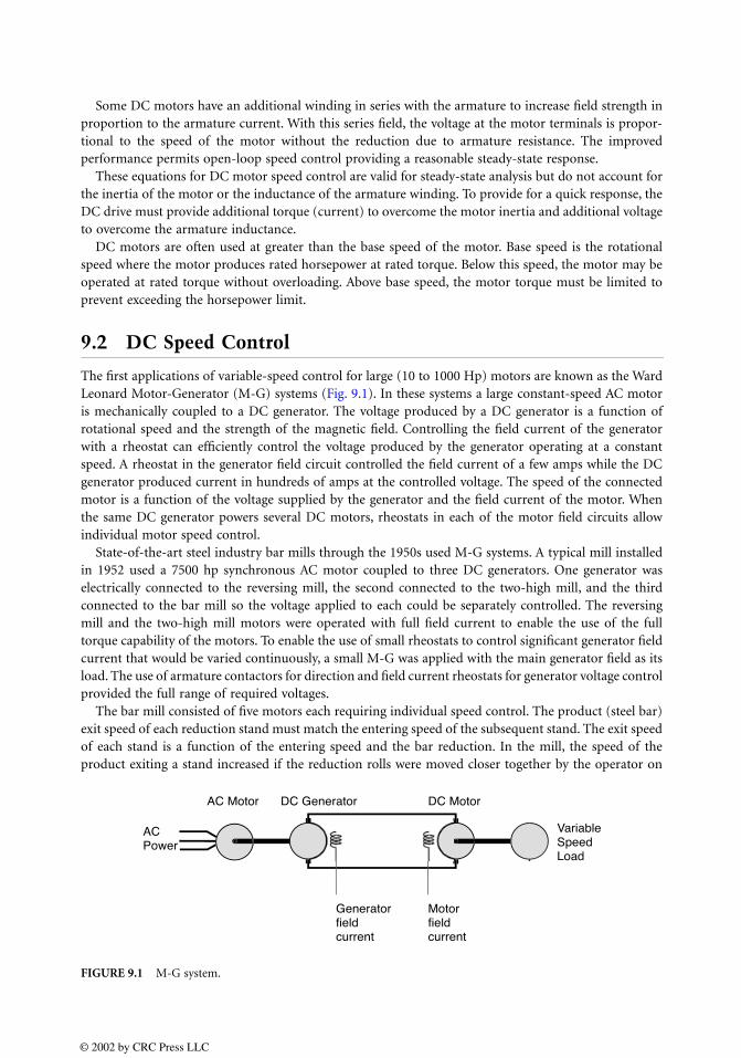
Some DC motors have an additional winding in series with the armature to increase field strength inproportion to the armature current. With this series field, the voltage at the motor terminals is propor-tional to the speed of the motor without the reduction due to armature resistance. The improvedperformance permits open-loop speed control providing a reasonable steady-state response.
These equations for DC motor speed control are valid for steady-state analysis but do not account forthe inertia of the motor or the inductance of the armature winding. To provide for a quick response, theDC drive must provide additional torque (current) to overcome the motor inertia and additional voltageto overcome the armature inductance.
DC motors are often used at greater than the base speed of the motor. Base speed is the rotationalspeed where the motor produces rated horsepower at rated torque. Below this speed, the motor may beoperated at rated torque without overloading. Above base speed, the motor torque must be limited toprevent exceeding the horsepower limit.
9.2 DC Speed Control
The first applications of variable-speed control for large (10 to 1000 Hp) motors are known as the WardLeonard Motor-Generator (M-G) systems (Fig. 9.1). In these systems a large constant-speed AC motoris mechanically coupled to a DC generator. The voltage produced by a DC generator is a function ofrotational speed and the strength of the magnetic field. Controlling the field current of the generatorwith a rheostat can efficiently control the voltage produced by the generator operating at a constantspeed. A rheostat in the generator field circuit controlled the field current of a few amps while the DCgenerator produced current in hundreds of amps at the controlled voltage. The speed of the connectedmotor is a function of the voltage supplied by the generator and the field current of the motor. Whenthe same DC generator powers several DC motors, rheostats in each of the motor field circuits allowindividual motor speed control.
State-of-the-art steel industry bar mills through the 1950s used M-G systems. A typical mill installedin 1952 used a 7500 hp synchronous AC motor coupled to three DC generators. One generator waselectrically connected to the reversing mill, the second connected to the two-high mill, and the thirdconnected to the bar mill so the voltage applied to each could be separately controlled. The reversingmill and the two-high mill motors were operated with full field current to enable the use of the fulltorque capability of the motors. To enable the use of small rheostats to control significant generator fieldcurrent that would be varied continuously, a small M-G was applied with the main generator field as itsload. The use of armature contactors for direction and field current rheostats for generator voltage controlprovided the full range of required voltages.
The bar mill consisted of five motors each requiring individual speed control. The product (steel bar)exit speed of each reduction stand must match the entering speed of the subsequent stand. The exit speedof each stand is a function of the entering speed and the bar reduction. In the mill, the speed of theproduct exiting a stand increased if the reduction rolls were moved closer together by the operator on
FIGURE 9.1 M-G system.
© 2002 by CRC Press LLC
the production floor. As the floor operator adjusted the roll gap to produce the proper size, the fieldcurrents required adjustment. A second operator would monitor the size of the loop formed betweenthe stands and adjust the rheostats to compensate for the roll gap changes.
With the introduction of semiconductors, systems were installed to take advantage of the diode. Inthe 1960s, large DC motors were replacing steam power turbines at many mills. Rather than installing aM-G set, a diode bank and an associated transformer provided a constant DC power source. The DCmotor and gear reducers were selected to operate above base speed in the constant horsepower range.The goal was to increase efficiency and reduce maintenance costs. In the M-G set, both the AC motorand the DC generator were less then 100% efficient and each required maintenance of brushes andbearings. The solid-state constant DC voltage source increased efficiency and reduced maintenance costs.Speed regulation still used rheostats and the motor speed control was open loop. One significant disad-vantage of the diode DC voltage source compared with the M-G source was the inability to regeneratepower. Motor speed could not be reduced rapidly without having a bank of resistors to dissipate the excessenergy. The M-G set would convert from a consumer of electric power to a supplier when the load speedwas faster than the desired.
Transistor developments in the 1960s and 1970s brought further gains to large DC motor control.With the introduction of transistorized field current regulators, the motor speed was controlled electron-ically with a rapid closed-loop response. A small DC generator, referred to as a tachometer, provided avoltage proportional to the motor speed. The transistor field current regulator compared the tachometerfeedback to the speed set point and adjusted the field current to control the motor speed.
The use of rheostats and early transistor regulators were inefficient for speed control when applied inthe armature circuit. With the development of new systems using pulse width modulated (PWM) voltageregulators, the armature voltage for small motors could be controlled. Systems up to several horsepowerwere successfully applied to DC motors using permanent magnet fields. The power dissipated by thetransistor when gated-on is minimal and the power while gated-off is zero. However, the power the transistoris required to dissipate while turning on and off limited the size of these systems. The application of PWMtransistors as field current regulators to large DC motors of hundreds of horsepower provided the efficiencyand closed-loop response of transistorized control to large systems.
The introduction of thyristor or silicon-controlled rectifiers (SCRs) provided for the revolution incontrol of large DC motors. SCRs were applied in both the field current regulators and the armaturevoltage regulators. With the SCR came increased efficiency, the ability to regenerate power, and highpower capability. DC drives and motors from a few horsepower to hundreds of horsepower could beoperated and controlled efficiently in all four quadrants when powered by three-phase line voltage. Inaddition, systems were developed for DC-to-DC control for the operation of battery-powered equipment.
The latest development in the DC motor control is the introduction of the insulated gate bipolartransistor (IGBT) to large power systems. These transistors have a fast switching time that reduces thepower the transistor is required to dissipate. With the introduction of the IGBT came a movement to applythe concepts and lessons learned to large AC systems. Predictions were made that DC systems were obsoleteand would soon be replaced. However, DC systems have proved to be dependable and cost-effective. Theyare still being applied when the application is suitable for economic reasons.
9.3 DC Drive Basics
Speed regulation in analogue drives is accomplished with a proportional–integral–derivative (PID) reg-ulator for the voltage output. The input to the equation was the speed error and the output is used todrive the voltage regulator. A faster response is obtained by using the output of the PID equation as theinput to the current regulator. A second PID regulator uses the output of the current regulator as aninput to control the voltage. When additional speed is required, additional current is called for. Thecurrent regulator call for more voltage force increased current. The increased current provides additionaltorque resulting in increased speed.
© 2002 by CRC Press LLC
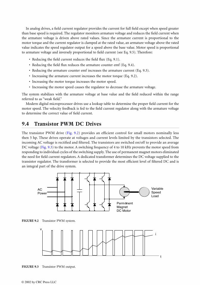
In analog drives, a field current regulator provides the current for full field except when speed greaterthan base speed is required. The regulator monitors armature voltage and reduces the field current whenthe armature voltage is driven above rated values. Since the armature current is proportional to themotor torque and the current regulator is clamped at the rated value, an armature voltage above the ratedvalue indicates the speed regulator output for a speed above the base value. Motor speed is proportionalto armature voltage and inversely proportional to field current (see Eq. 9.5). Therefore:
• Reducing the field current reduces the field flux (Eq. 9.1).
• Reducing the field flux reduces the armature counter emf (Eq. 9.4).
• Reducing the armature counter emf increases the armature current (Eq. 9.3).
• Increasing the armature current increases the motor torque (Eq. 9.2).
• Increasing the motor torque increases the motor speed.
• Increasing the motor speed causes the regulator to decrease the armature voltage.
The system stabilizes with the armature voltage at base value and the field reduced within the rangereferred to as “weak field.”
Modern digital microprocessor drives use a lookup table to determine the proper field current for themotor speed. The velocity feedback is fed to the field current regulator along with the armature voltageto determine the correct value of field current.
9.4 Transistor PWM DC Drives
The transistor PWM drive (Fig. 9.2) provides an efficient control for small motors nominally lessthen 5 hp. These drives operate at voltages and current levels limited by the transistors selected. Theincoming AC voltage is rectified and filtered. The transistors are switched on/off to provide an averageDC voltage (Fig. 9.3) to the motor. A switching frequency of 4 to 10 kHz prevents the motor speed fromresponding to individual cycles of the switching supply. The use of permanent magnet motors eliminatedthe need for field current regulators. A dedicated transformer determines the DC voltage supplied to thetransistor regulator. The transformer is selected to provide the most efficient level of filtered DC and isan integral part of the drive system.
FIGURE 9.2 Transistor PWM system.
FIGURE 9.3 Transistor PWM output.
a
t
v
i
© 2002 by CRC Press LLC
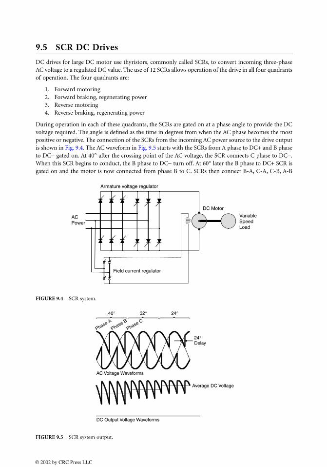
9.5 SCR DC Drives
DC drives for large DC motor use thyristors, commonly called SCRs, to convert incoming three-phaseAC voltage to a regulated DC value. The use of 12 SCRs allows operation of the drive in all four quadrantsof operation. The four quadrants are:
1. Forward motoring2. Forward braking, regenerating power3. Reverse motoring4. Reverse braking, regenerating power
During operation in each of these quadrants, the SCRs are gated on at a phase angle to provide the DCvoltage required. The angle is defined as the time in degrees from when the AC phase becomes the mostpositive or negative. The connection of the SCRs from the incoming AC power source to the drive outputis shown in Fig. 9.4. The AC waveform in Fig. 9.5 starts with the SCRs from A phase to DC+ and B phaseto DC− gated on. At 40° after the crossing point of the AC voltage, the SCR connects C phase to DC−.When this SCR begins to conduct, the B phase to DC− turn off. At 60° later the B phase to DC+ SCR isgated on and the motor is now connected from phase B to C. SCRs then connect B-A, C-A, C-B, A-B
FIGURE 9.4 SCR system.
FIGURE 9.5 SCR system output.
Average DC Voltage
40° 32° 24°
24°Delay
Phase A
Phase B
Phase C
AC Voltage Waveforms
DC Output Voltage Waveforms
© 2002 by CRC Press LLC
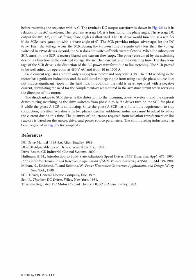
before restarting the sequence with A-C. The resultant DC output waveform is shown in Fig. 9.5 as is itsrelation to the AC waveform. The resultant average DC is a function of the phase angle. The average DCoutput for 40°, 32°, and 24° firing phase angles is illustrated. The DC drive would function as a rectifierif the SCRs were gated on with a phase angle of 0°. The SCR provides unique advantages for the DCdrive. First, the voltage across the SCR during the turn-on time is significantly less than the voltageswitched in PWM drives. Second, the SCR does not switch off with current flowing. When the subsequentSCR turns on, the SCR is reverse-biased and current flow stops. The power consumed by the switchingdevice is a function of the switched voltage, the switched current, and the switching time. The disadvan-tage of the SCR drive is the distortion of the AC power waveform due to line notching. The SCR provedto be well suited for operation at 480 V AC and from 10 to 1000 A.
Field current regulators require only single-phase power and only four SCRs. The field winding in themotor has significant inductance and the additional voltage ripple from using a single-phase source doesnot induce significant ripple in the field flux. In addition, the field is never operated with a negativecurrent, eliminating the need for the complementary set required in the armature circuit when reversingthe direction of the motor.
The disadvantage to SCR drives is the distortion to the incoming power waveform and the currentsdrawn during switching. As the drive switches from phase A to B, the drives turn on the SCR for phaseB while the phase A SCR is conducting. Since the phase A SCR has a finite time requirement to stopconduction, this effectively shorts the two phases together. Additional inductance must be added to reducethe current during this time. The quantity of inductance required from isolation transformers or linereactors is based on the motor, drive, and power source parameters. The commutating inductance hasbeen neglected in Fig. 9.5 for simplicity.
References
DC Drive Manual 1395-5.6, Allen-Bradley, 1989.DC-300 Adjustable Speed Drives, General Electric, 1988.Drive Basics, GE Industrial Control Systems, 2000.Huffman, H. H., Introduction to Solid-State Adjustable Speed Drives, IEEE Trans. Ind. Appl., 671, 1990.IEEE Guide for Harmonic and Reactive Compensation of Static Power Converters, ANSI/IEEE Std 519-1981.Mohan, N., Undeland, T., and Robbins, W., Power Electronics: Converters, Applications, and Design, Wiley,
New York, 1989.SCR Drives, General Electric Company, Erie, 1975.Sen, P., Thyristor DC Drives, Wiley, New York, 1981.Thyristor Regulated DC Motor Control Theory, DGI-2.0, Allen-Bradley, 1982.
© 2002 by CRC Press LLC
10AC MachinesControlled asDC Machines(Brushless DC
Machines/Electronics)
10.1 Introduction10.2 Machine Construction
Permanent Magnets • Stator Windings
10.3 Motor CharacteristicsMathematical Model
10.4 Power Electronic ConverterUnipolar Excitation • Fault-Tolerant Configuration • Current Source Inverter
10.5 Position SensingPosition Sensorless Control
10.6 Pulsating Torque Components10.7 Torque-Speed Characteristics10.8 Applications
10.1 Introduction
Brushless DC (BLDC) motors are synchronous motors with permanent magnets on the rotor andarmature windings on the stator. Hence, from a construction point of view, they are the inside-out versionof DC motors, which have permanent magnets or field windings on the stator and armature windingson the rotor. A typical BLDC motor with 12 stator slots and four poles on the rotor is shown in Fig. 10.1.
The most obvious advantage of the brushless configuration is the removal of the brushes, whicheliminates brush maintenance and the sparking associated with them. Having the armature windings onthe stator helps the conduction of heat from the windings. Because there are no windings on the rotor,electrical losses in the rotor are minimal. The BLDC motor compares favorably with induction motorsin the fractional horsepower range. The former will have better efficiency and better power factor and,therefore, a greater output power for the same frame, because the field excitation is contributed by thepermanent magnets and does not have to be supplied by the armature current.
These advantages of the BLDC motor come at the expense of increased complexity in the electroniccontroller and the need for shaft position sensing. Permanent magnet (PM) excitation is more viable insmaller motors, usually below 20 kW. In larger motors, the cost and weight of the magnets become
Hamid A. ToliyatTexas A&M University
Tilak GopalarathnamTexas A&M University
© 2002 by CRC Press LLC
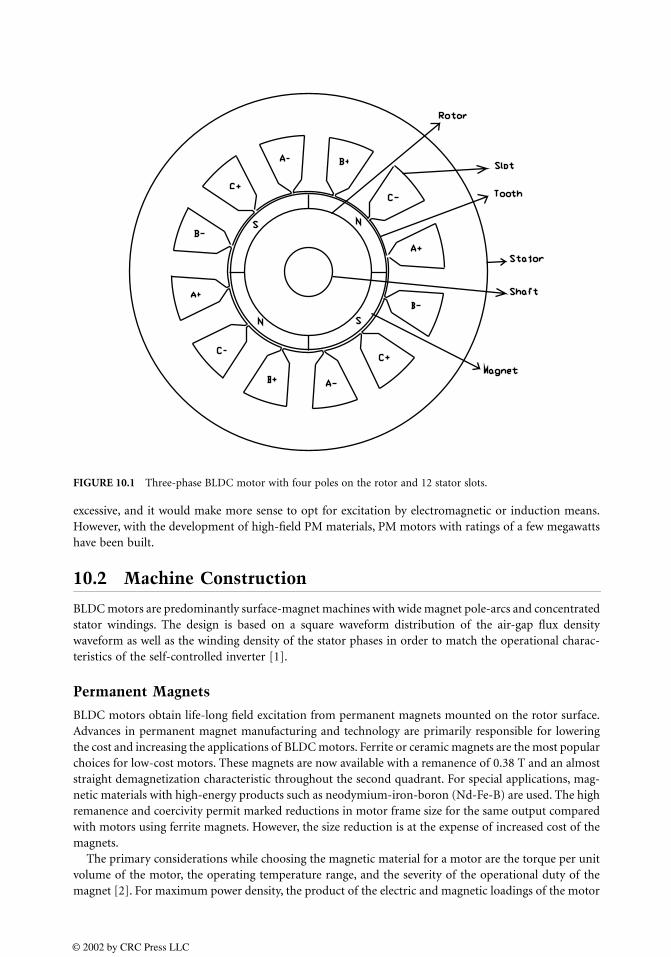
excessive, and it would make more sense to opt for excitation by electromagnetic or induction means.However, with the development of high-field PM materials, PM motors with ratings of a few megawattshave been built.
10.2 Machine Construction
BLDC motors are predominantly surface-magnet machines with wide magnet pole-arcs and concentratedstator windings. The design is based on a square waveform distribution of the air-gap flux densitywaveform as well as the winding density of the stator phases in order to match the operational charac-teristics of the self-controlled inverter [1].
Permanent Magnets
BLDC motors obtain life-long field excitation from permanent magnets mounted on the rotor surface.Advances in permanent magnet manufacturing and technology are primarily responsible for loweringthe cost and increasing the applications of BLDC motors. Ferrite or ceramic magnets are the most popularchoices for low-cost motors. These magnets are now available with a remanence of 0.38 T and an almoststraight demagnetization characteristic throughout the second quadrant. For special applications, mag-netic materials with high-energy products such as neodymium-iron-boron (Nd-Fe-B) are used. The highremanence and coercivity permit marked reductions in motor frame size for the same output comparedwith motors using ferrite magnets. However, the size reduction is at the expense of increased cost of themagnets.
The primary considerations while choosing the magnetic material for a motor are the torque per unitvolume of the motor, the operating temperature range, and the severity of the operational duty of themagnet [2]. For maximum power density, the product of the electric and magnetic loadings of the motor
FIGURE 10.1 Three-phase BLDC motor with four poles on the rotor and 12 stator slots.
© 2002 by CRC Press LLC
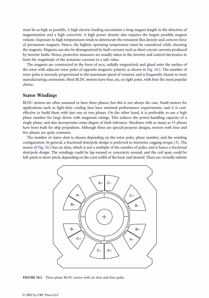
must be as high as possible. A high electric loading necessitates a long magnet length in the direction ofmagnetization and a high coercivity. A high power density also requires the largest possible magnetvolume. Exposure to high temperatures tends to deteriorate the remanent flux density and coercive forceof permanent magnets. Hence, the highest operating temperature must be considered while choosingthe magnets. Magnets can also be demagnetized by fault currents such as short-circuit currents producedby inverter faults. Hence, protective measures are usually taken in the inverter and control electronics tolimit the magnitude of the armature currents to a safe value.
The magnets are constructed in the form of arcs, radially magnetized, and glued onto the surface ofthe rotor with adjacent rotor poles of opposite magnetic polarity as shown in Fig. 10.1. The number ofrotor poles is inversely proportional to the maximum speed of rotation, and is frequently chosen to meetmanufacturing constraints. Most BLDC motors have four, six, or eight poles, with four the most popularchoice.
Stator Windings
BLDC motors are often assumed to have three phases, but this is not always the case. Small motors forapplications such as light-duty cooling fans have minimal performance requirements, and it is cost-effective to build them with just one or two phases. On the other hand, it is preferable to use a highphase number for large drives with megawatt ratings. This reduces the power-handling capacity of asingle phase, and also incorporates some degree of fault tolerance. Machines with as many as 15 phaseshave been built for ship propulsion. Although these are special-purpose designs, motors with four andfive phases are quite common.
The number of stator slots is chosen depending on the rotor poles, phase number, and the windingconfiguration. In general, a fractional slots/pole design is preferred to minimize cogging torque [3]. Themotor of Fig. 10.2 has six slots, which is not a multiple of the number of poles, and is hence a fractionalslots/pole design. The windings could be lap-wound or concentric-wound, and the coil span could befull-pitch or short-pitch, depending on the crest width of the back-emf desired. There are virtually infinite
FIGURE 10.2 Three-phase BLDC motor with six slots and four poles.
A+
A−
A+
A−
C−
C−
C+
C+
B−
B−
B+
B+
© 2002 by CRC Press LLC
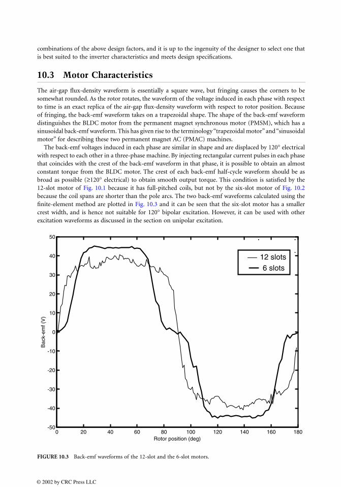
combinations of the above design factors, and it is up to the ingenuity of the designer to select one thatis best suited to the inverter characteristics and meets design specifications.
10.3 Motor Characteristics
The air-gap flux-density waveform is essentially a square wave, but fringing causes the corners to besomewhat rounded. As the rotor rotates, the waveform of the voltage induced in each phase with respectto time is an exact replica of the air-gap flux-density waveform with respect to rotor position. Becauseof fringing, the back-emf waveform takes on a trapezoidal shape. The shape of the back-emf waveformdistinguishes the BLDC motor from the permanent magnet synchronous motor (PMSM), which has asinusoidal back-emf waveform. This has given rise to the terminology “trapezoidal motor” and “sinusoidalmotor” for describing these two permanent magnet AC (PMAC) machines.
The back-emf voltages induced in each phase are similar in shape and are displaced by 120° electricalwith respect to each other in a three-phase machine. By injecting rectangular current pulses in each phasethat coincides with the crest of the back-emf waveform in that phase, it is possible to obtain an almostconstant torque from the BLDC motor. The crest of each back-emf half-cycle waveform should be asbroad as possible (≥120° electrical) to obtain smooth output torque. This condition is satisfied by the12-slot motor of Fig. 10.1 because it has full-pitched coils, but not by the six-slot motor of Fig. 10.2because the coil spans are shorter than the pole arcs. The two back-emf waveforms calculated using thefinite-element method are plotted in Fig. 10.3 and it can be seen that the six-slot motor has a smallercrest width, and is hence not suitable for 120° bipolar excitation. However, it can be used with otherexcitation waveforms as discussed in the section on unipolar excitation.
FIGURE 10.3 Back-emf waveforms of the 12-slot and the 6-slot motors.
0 20 40 60 80 100 120 140 160 180-50
-40
-30
-20
-10
0
10
20
30
40
50
Bac
k-em
f (V
)
Rotor position (deg)
12 slots
6 slots
© 2002 by CRC Press LLC

The ideal back-emf voltage and 120° phase current waveforms for a three-phase BLDC motor areshown in Fig. 10.4. The inverter switches that are active during each 60° interval are also shown corre-sponding to the inverter circuit of Fig. 10.5. The simplicity of this scheme arises from the fact that duringany conduction interval, there is only one current flowing through two phases of the machine, whichcan be sensed using a single current sensor in the DC link. Because there are only two inverter switchesactive at any time, this is also called the two-switch conduction scheme, as opposed to the three-switchconduction scheme used in PMSM motor drives.
The amplitude of the phase back-emf is proportional to the rotor speed, and is given by
(10.1)
FIGURE 10.4 Back-emf and phase current waveforms for three-phase BLDC motor with 120° bipolar currents.
FIGURE 10.5 Schematic of IGBT-based inverter for three-phase BLDC motor.
EI Phase A
Phase B
Phase C
360180
S5S6
S1S6
S1S2
S3S2
S3S4
S5S4
S5S6
Activeswitches
T eTorque
B L D CMotor
S1 S3 S5
S4 S6 S2
D 2D6D4
D1 D3 D5
ph A
ph B
ph C
+
-
Vdc
E kfwm=
© 2002 by CRC Press LLC

where k is a constant that depends on the number of turns in each phase, φ is the permanent magnetflux, and ωm is the mechanical speed.
During any 120° interval, the instantaneous power being converted from electrical to mechanical isthe sum of the contributions from two phases in series, and is given by
(10.2)
where Te is the output torque and I is the amplitude of the phase current. From Eqs. (10.1) and (10.2),the expression for output torque can be written as
(10.3)
where kt is the torque constant. The similarity between the BLDC motor and the commutator DC motor can be seen from Eqs. (10.1)
and (10.3). It is because of this similarity in control characteristics that the trapezoidal PMAC motor iswidely known as the BLDC motor, although this term is a misnomer as it is actually a synchronous ACmotor. But it is also not a rotating field machine in the AC sense, because the armature mmf rotates indiscrete steps of 60° electrical as opposed to a smooth rotation in other AC machines.
Mathematical Model
Because of the nonsinusoidal nature of the back-emf and current waveforms, transformation of themachine equations to the d-q model is cumbersome, and it is easier to use the phase-variable approachfor modeling and simulation. The back-emf can be represented as a Fourier series or by using piecewiselinear curves [4]. The circuit equations of the three windings in phase variables can be written as [4]
(10.4)
where va, vb, vc are the phase voltages, ia, ib, ic are the phase currents, ea, eb, ec are the phase back-emfvoltages, R is the phase resistance, L is the self-inductance of each phase, and M is the mutual inductancebetween any two phases.
The electromagnetic torque is given by
(10.5)
where ωm is the mechanical speed of the rotor.The equation of motion is
(10.6)
where TL is the load torque, B is the damping constant, and J is the moment of inertia of the drive.The electrical frequency is related to the mechanical speed by
(10.7)
where P is the number of rotor poles.
Po wmTe 2EI= =
Te 2kfI ktI= =
va
vb
vc
R 0 0
0 R 0
0 0 R
ia
ib
ic
L M– 0 0
0 L M– 0
0 0 L M–
ddt-----
ia
ib
ic
ea
eb
ec
++⋅=
Te eaia ebib ecic+ +( )/wm=
ddt----- wm Te TL Bwm––( )/J=
we P/2( )wm=
© 2002 by CRC Press LLC
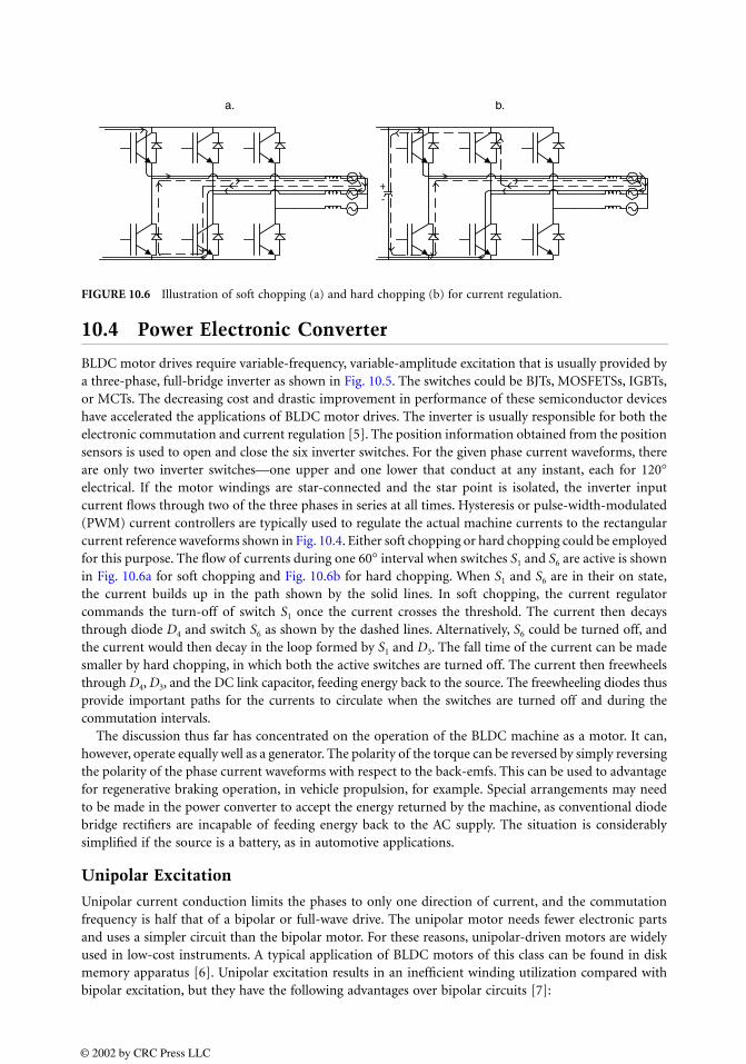
10.4 Power Electronic Converter
BLDC motor drives require variable-frequency, variable-amplitude excitation that is usually provided bya three-phase, full-bridge inverter as shown in Fig. 10.5. The switches could be BJTs, MOSFETSs, IGBTs,or MCTs. The decreasing cost and drastic improvement in performance of these semiconductor deviceshave accelerated the applications of BLDC motor drives. The inverter is usually responsible for both theelectronic commutation and current regulation [5]. The position information obtained from the positionsensors is used to open and close the six inverter switches. For the given phase current waveforms, thereare only two inverter switches—one upper and one lower that conduct at any instant, each for 120°electrical. If the motor windings are star-connected and the star point is isolated, the inverter inputcurrent flows through two of the three phases in series at all times. Hysteresis or pulse-width-modulated(PWM) current controllers are typically used to regulate the actual machine currents to the rectangularcurrent reference waveforms shown in Fig. 10.4. Either soft chopping or hard chopping could be employedfor this purpose. The flow of currents during one 60° interval when switches S1 and S6 are active is shownin Fig. 10.6a for soft chopping and Fig. 10.6b for hard chopping. When S1 and S6 are in their on state,the current builds up in the path shown by the solid lines. In soft chopping, the current regulatorcommands the turn-off of switch S1 once the current crosses the threshold. The current then decaysthrough diode D4 and switch S6 as shown by the dashed lines. Alternatively, S6 could be turned off, andthe current would then decay in the loop formed by S1 and D3. The fall time of the current can be madesmaller by hard chopping, in which both the active switches are turned off. The current then freewheelsthrough D4, D3, and the DC link capacitor, feeding energy back to the source. The freewheeling diodes thusprovide important paths for the currents to circulate when the switches are turned off and during thecommutation intervals.
The discussion thus far has concentrated on the operation of the BLDC machine as a motor. It can,however, operate equally well as a generator. The polarity of the torque can be reversed by simply reversingthe polarity of the phase current waveforms with respect to the back-emfs. This can be used to advantagefor regenerative braking operation, in vehicle propulsion, for example. Special arrangements may needto be made in the power converter to accept the energy returned by the machine, as conventional diodebridge rectifiers are incapable of feeding energy back to the AC supply. The situation is considerablysimplified if the source is a battery, as in automotive applications.
Unipolar Excitation
Unipolar current conduction limits the phases to only one direction of current, and the commutationfrequency is half that of a bipolar or full-wave drive. The unipolar motor needs fewer electronic partsand uses a simpler circuit than the bipolar motor. For these reasons, unipolar-driven motors are widelyused in low-cost instruments. A typical application of BLDC motors of this class can be found in diskmemory apparatus [6]. Unipolar excitation results in an inefficient winding utilization compared withbipolar excitation, but they have the following advantages over bipolar circuits [7]:
FIGURE 10.6 Illustration of soft chopping (a) and hard chopping (b) for current regulation.
-+
a. b.
© 2002 by CRC Press LLC

1. There is only one device in series with each phase, minimizing conduction losses.2. The risk of shoot-through faults is eliminated.3. Switching of devices connected to the supply rails, which generally requires some isolation cir-
cuitry, can be avoided.
Another factor that has to be considered before choosing unipolar excitation is that the motor neutralhas to be available because the phase currents are no longer balanced. The main issue in unipolar BLDCmotor drives is ripple torque. The reference case of the 12-slot motor with 120° bipolar currents gives aripple torque of 13%. This value represents the ripple component caused by the nonideal back-emf alone,without considering inverter effects. Exciting the same motor with 120° unipolar currents, for example,would produce a torque ripple of 23.7%. However, by exciting the six-slot motor with the 180° unipolarcurrent waveforms shown in Fig. 10.7, the torque ripple reduces to 8.5% [8]. It is thus important tomatch the motor characteristics to those of the inverter. Increasing the number of phases can also reducethe torque pulsation, but the cost of the drive increases. The simplest unipolar converter has a singleswitch in series with each motor winding, whereas a reverse-parallel diode provides a freewheeling pathat turn-off. This drive has no regenerative control, but four-quadrant operation is possible by usingtopologies with more than one switch per phase but fewer than two switches per phase [9]. One suchtopology that has been used for switched reluctance drives is the C-dump converter shown in Fig. 10.8.
Fault-Tolerant Configuration
In applications requiring high reliability such as aerospace and defense, the inverter may be configuredas a separate H-bridge supplying each phase of the motor as shown in Fig. 10.9. This doubles the numberof power devices, but ensures complete electrical isolation between phases so that remedial strategies canbe adopted to continue operation even with the failure of a power device or winding [10]. It is alsoimportant to design the machine to minimize the occurrence of a fault by winding each coil around asingle tooth. High phase numbers are also used so that the healthy phases can partially compensate forthe loss of torque resulting from the failure of one or more phases.
Current Source Inverter
As an alternative to the voltage source inverter (VSI), a current source inverter may be used to drive theBLDC motor. A load-commutated inverter as shown in Fig. 10.10 uses thyristors as the switching devices,and is cheaper than a VSI of similar rating [11]. It replaces the DC-link electrolytic capacitor by an inductor.
FIGURE 10.7 180° unipolar current waveforms.
FIGURE 10.8 Schematic of C-dump topology for unipolar three-phase BLDC motor.
I phase A
360180phase B
phase C
ωt
+_Vdc Cda b c
T1 T2 T3D1
D2D3
D4
T4
Co
Lo
© 2002 by CRC Press LLC
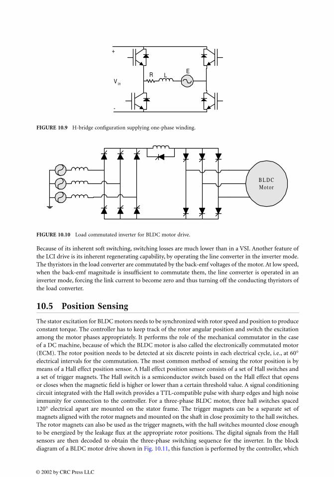
Because of its inherent soft switching, switching losses are much lower than in a VSI. Another feature ofthe LCI drive is its inherent regenerating capability, by operating the line converter in the inverter mode.The thyristors in the load converter are commutated by the back-emf voltages of the motor. At low speed,when the back-emf magnitude is insufficient to commutate them, the line converter is operated in aninverter mode, forcing the link current to become zero and thus turning off the conducting thyristors ofthe load converter.
10.5 Position Sensing
The stator excitation for BLDC motors needs to be synchronized with rotor speed and position to produceconstant torque. The controller has to keep track of the rotor angular position and switch the excitationamong the motor phases appropriately. It performs the role of the mechanical commutator in the caseof a DC machine, because of which the BLDC motor is also called the electronically commutated motor(ECM). The rotor position needs to be detected at six discrete points in each electrical cycle, i.e., at 60°electrical intervals for the commutation. The most common method of sensing the rotor position is bymeans of a Hall effect position sensor. A Hall effect position sensor consists of a set of Hall switches anda set of trigger magnets. The Hall switch is a semiconductor switch based on the Hall effect that opensor closes when the magnetic field is higher or lower than a certain threshold value. A signal conditioningcircuit integrated with the Hall switch provides a TTL-compatible pulse with sharp edges and high noiseimmunity for connection to the controller. For a three-phase BLDC motor, three hall switches spaced120° electrical apart are mounted on the stator frame. The trigger magnets can be a separate set ofmagnets aligned with the rotor magnets and mounted on the shaft in close proximity to the hall switches.The rotor magnets can also be used as the trigger magnets, with the hall switches mounted close enoughto be energized by the leakage flux at the appropriate rotor positions. The digital signals from the Hallsensors are then decoded to obtain the three-phase switching sequence for the inverter. In the blockdiagram of a BLDC motor drive shown in Fig. 10.11, this function is performed by the controller, which
FIGURE 10.9 H-bridge configuration supplying one-phase winding.
FIGURE 10.10 Load commutated inverter for BLDC motor drive.
+
-
R LE
V in
B L D CM o t o r
© 2002 by CRC Press LLC
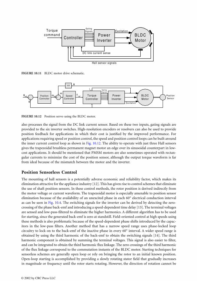
also processes the signal from the DC link current sensor. Based on these two inputs, gating signals areprovided to the six inverter switches. High-resolution encoders or resolvers can also be used to provideposition feedback for applications in which their cost is justified by the improved performance. Forapplications requiring speed or position control, the speed and position control loops can be built aroundthe inner current control loop as shown in Fig. 10.12. The ability to operate with just three Hall sensorsgives the trapezoidal brushless permanent magnet motor an edge over its sinusoidal counterpart in low-cost applications. It should be mentioned that PMSM motors are also sometimes operated with rectan-gular currents to minimize the cost of the position sensor, although the output torque waveform is farfrom ideal because of the mismatch between the motor and the inverter.
Position Sensorless Control
The mounting of hall sensors is a potentially adverse economic and reliability factor, which makes itselimination attractive for the appliance industry [12]. This has given rise to control schemes that eliminatethe use of shaft position sensors. In these control methods, the rotor position is derived indirectly fromthe motor voltage or current waveform. The trapezoidal motor is especially amenable to position sensorelimination because of the availability of an unexcited phase in each 60° electrical conduction intervalas can be seen in Fig. 10.4. The switching signals for the inverter can be derived by detecting the zero-crossing of the phase back-emf and introducing a speed-dependent time delay [13]. The terminal voltagesare sensed and low-pass-filtered to eliminate the higher harmonics. A different algorithm has to be usedfor starting, since the generated back-emf is zero at standstill. Field-oriented control at high speeds usingthese methods is also problematic because of the speed-dependent phase shifts introduced by the capac-itors in the low-pass filters. Another method that has a narrow speed range uses phase-locked loopcircuitry to lock on to the back-emf of the inactive phase in every 60° interval. A wider speed range isobtained by using the third harmonic of the back-emf to obtain the switching signals [14]. The thirdharmonic component is obtained by summing the terminal voltages. This signal is also easier to filter,and can be integrated to obtain the third harmonic flux linkage. The zero crossings of the third harmonicof the flux linkage correspond to the commutation instants of the BLDC motor. Starting techniques forsensorless schemes are generally open loop or rely on bringing the rotor to an initial known position.Open-loop starting is accomplished by providing a slowly rotating stator field that gradually increasesin magnitude or frequency until the rotor starts rotating. However, the direction of rotation cannot be
FIGURE 10.11 BLDC motor drive schematic.
FIGURE 10.12 Position servo using the BLDC motor.
B L D CMotor
PowerInverter
Torquecommand
Excitation
Control ler
DC l ink current sense
Hall sensor signals
Gat ingSignals
BLDCMotor
PowerInverter
T ref
Excitation
TorqueControl ler
Gat ingSignals
Posit ionSensor
SpeedController
+-ωrefPosit ion
Controller-+θref
Iφ
d/dt
ω
θ
θ
© 2002 by CRC Press LLC

controlled using this method. This disadvantage can be overcome by exciting one phase to bring the rotorto a known initial position before applying the rotating stator field. There are several commercially availableintegrated circuits that use the back-emf sensing technique for sensorless control. The availability of fastdigital signal processor (DSP) controllers has enabled the implementation of many computationally intensivealgorithms for rotor position sensing.
10.6 Pulsating Torque Components
One of the drawbacks of the BLDC motor drive is its relatively high torque pulsation. Its pulsating torquecomponents can be classified as cogging and ripple torques, which are produced by essentially differentphenomena. Cogging torque is produced by the reluctance variation caused by the stator slot openingsas the rotor rotates. It is space dependent, and exists even in the absence of any armature current. It iswell known that skewing of the stator slots or rotor magnets by one slot pitch reduces cogging to afraction of 1% of the rated torque [15]. Cogging can also be minimized without skewing by choosing afractional slots/pole motor design [3], or by an appropriate choice of the magnet width relative to theslot pitch [16]. But any technique used to reduce the cogging torque generally results in more rippletorque due to a departure from the ideal trapezoidal induced emf. Ripple torque is a consequence ofthe interaction of armature currents with the machine back-emf waveforms. There are three maincomponents of ripple torque, one motor-related and the other two inverter-related. The motor-relatedcomponent is produced by the non-idealities in the back-emf waveform. It is desirable to minimizethis component by designing the machine so that the crest of the back-emf waveform is as wide andflat as possible. The inverter-related components of ripple torque appear because of a departure fromthe ideal rectangular current profiles due to the finite inductance of the machine windings. The firstinverter-related component is caused by the high-frequency current ripple that is present because of thecurrent hysteresis or PWM control of the inverter. This component is usually filtered out by the loadinertia, and so is generally not a problem. The second component is the commutation torque ripple,which occurs at every commutation instant. It develops because the sum of the currents in the off-goingand oncoming phases is almost never constant during the commutation intervals. This is illustrated inFig. 10.13, where the current is commutated from phase “b” to phase “c.” The rate at which the currentbuilds up in phase “c” is greater than the rate at which it decays in phase “b,” which causes a currentspike in phase “a,” and a corresponding spike in the torque waveform. Commutation torque ripple appearsas spikes or dips depending on the rotor speed and source voltage [17]. Control techniques to minimizethis component generally involve using a current sensor in each phase [18], but it is more cost-effectiveto use a single current sensor in the DC link. A single current sensor would also be unable to detecttransient overcurrents in the inverter switches, and so the current control scheme has to be modified toprotect the switches [19]. Figure 10.14 shows the waveforms of the phase current and the electromagnetictorque under hysteresis current control. All three ripple torque components are visible here. The high-frequency ripple component is caused by the corresponding ripple in the phase current. The back-emf-related component has a frequency that is six times the electrical frequency, corresponding to the sixconduction intervals in each cycle. The commutation torque ripple appears as spikes in the torquewaveform at every commutation instant. At high speeds, these ripples may be filtered out by the loadinertia, but at low speeds, they can affect the performance of the drive severely. This makes the BLDCmotor drive unsuitable for high-performance positioning applications, where accuracy and repeatabilitywould be compromised by torque pulsations.
10.7 Torque-Speed Characteristics
BLDC motors are ideally suited for constant-torque applications, as the field excitation is fixed and thetorque is proportional to the armature current. However, operation beyond the base speed in the constantpower region as shown in Fig. 10.15 is also desirable in many cases, and for this, fixed field excitation isa disadvantage, as discussed below. Current control is based on a positive voltage difference between the
© 2002 by CRC Press LLC
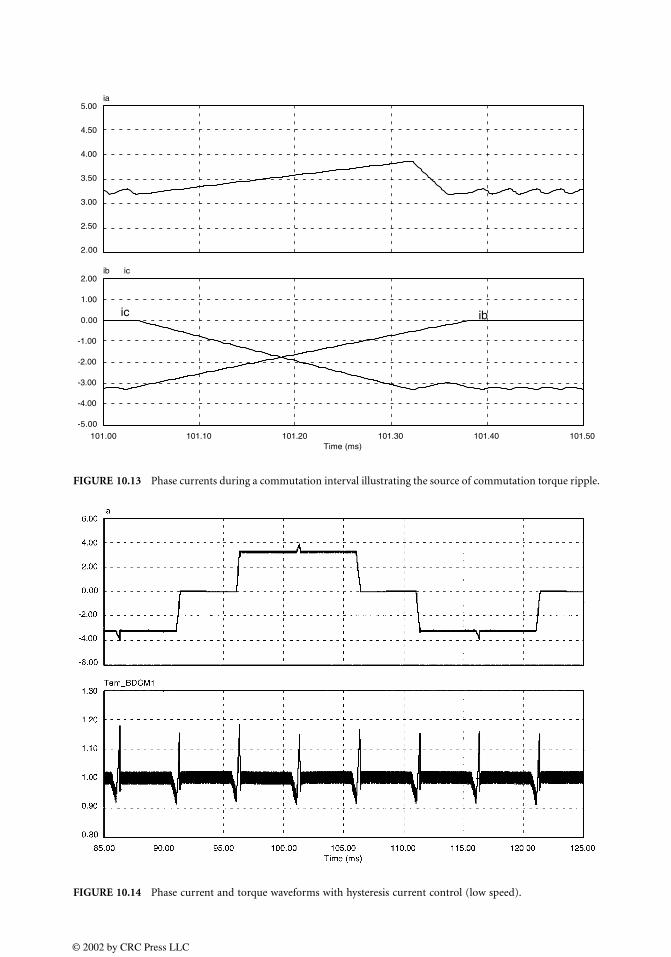
FIGURE 10.13 Phase currents during a commutation interval illustrating the source of commutation torque ripple.
FIGURE 10.14 Phase current and torque waveforms with hysteresis current control (low speed).
2.00
2.50
3.00
3.50
4.00
4.50
5.00ia
101.00 101.10 101.20 101.30 101.40 101.50
-5.00
-4.00
-3.00
-2.00
-1.00
0.00
1.00
2.00
Time (ms)
ib ic
ibic
© 2002 by CRC Press LLC
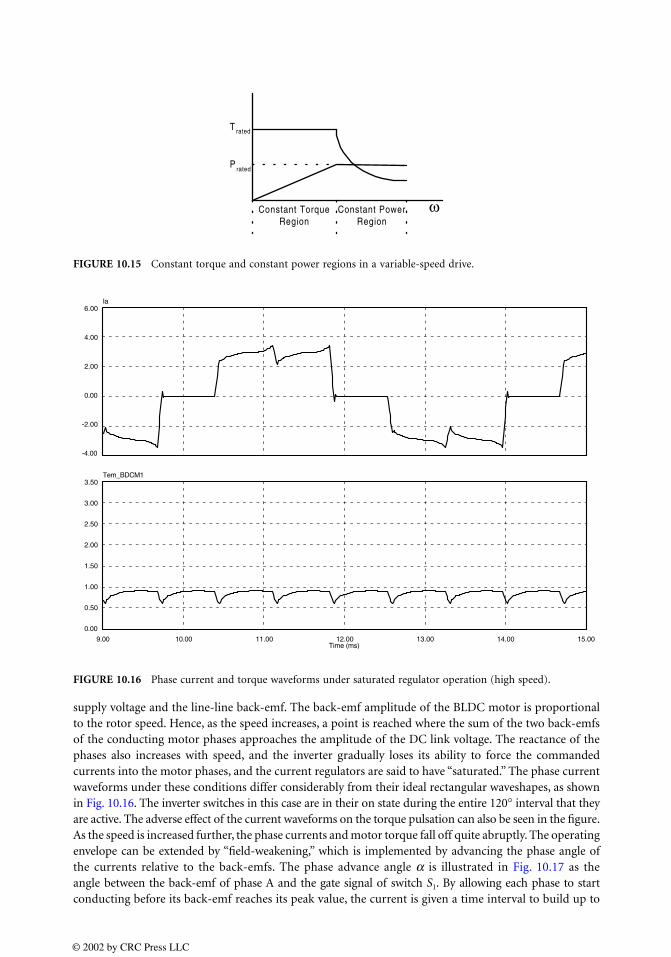
supply voltage and the line-line back-emf. The back-emf amplitude of the BLDC motor is proportionalto the rotor speed. Hence, as the speed increases, a point is reached where the sum of the two back-emfsof the conducting motor phases approaches the amplitude of the DC link voltage. The reactance of thephases also increases with speed, and the inverter gradually loses its ability to force the commandedcurrents into the motor phases, and the current regulators are said to have “saturated.” The phase currentwaveforms under these conditions differ considerably from their ideal rectangular waveshapes, as shownin Fig. 10.16. The inverter switches in this case are in their on state during the entire 120° interval that theyare active. The adverse effect of the current waveforms on the torque pulsation can also be seen in the figure.As the speed is increased further, the phase currents and motor torque fall off quite abruptly. The operatingenvelope can be extended by “field-weakening,” which is implemented by advancing the phase angle ofthe currents relative to the back-emfs. The phase advance angle α is illustrated in Fig. 10.17 as theangle between the back-emf of phase A and the gate signal of switch S1. By allowing each phase to startconducting before its back-emf reaches its peak value, the current is given a time interval to build up to
FIGURE 10.15 Constant torque and constant power regions in a variable-speed drive.
FIGURE 10.16 Phase current and torque waveforms under saturated regulator operation (high speed).
Constant TorqueRegion
Constant PowerRegion
T rated
P rated
ω
-4.00
-2.00
0.00
2.00
4.00
6.00Ia
9.00 10.00 11.00 12.00 13.00 14.00 15.00
0.00
0.50
1.00
1.50
2.00
2.50
3.00
3.50
Time (ms)
Tem_BDCM1
© 2002 by CRC Press LLC
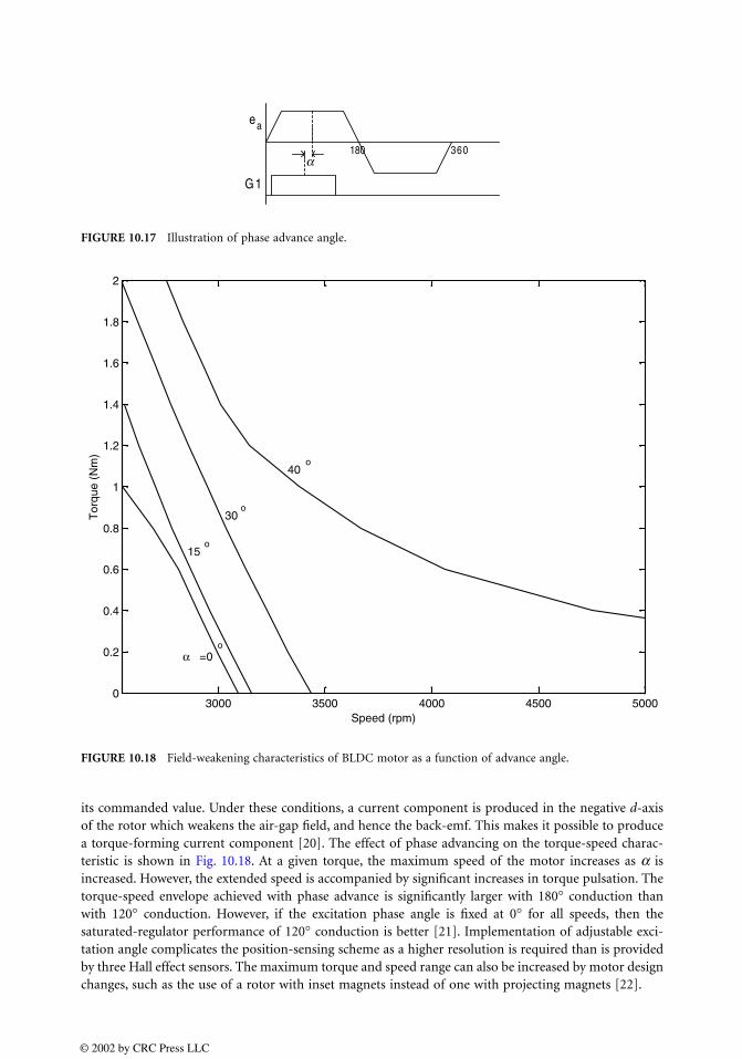
its commanded value. Under these conditions, a current component is produced in the negative d-axisof the rotor which weakens the air-gap field, and hence the back-emf. This makes it possible to producea torque-forming current component [20]. The effect of phase advancing on the torque-speed charac-teristic is shown in Fig. 10.18. At a given torque, the maximum speed of the motor increases as α isincreased. However, the extended speed is accompanied by significant increases in torque pulsation. Thetorque-speed envelope achieved with phase advance is significantly larger with 180° conduction thanwith 120° conduction. However, if the excitation phase angle is fixed at 0° for all speeds, then thesaturated-regulator performance of 120° conduction is better [21]. Implementation of adjustable exci-tation angle complicates the position-sensing scheme as a higher resolution is required than is providedby three Hall effect sensors. The maximum torque and speed range can also be increased by motor designchanges, such as the use of a rotor with inset magnets instead of one with projecting magnets [22].
FIGURE 10.17 Illustration of phase advance angle.
FIGURE 10.18 Field-weakening characteristics of BLDC motor as a function of advance angle.
360180α
ea
G1
3000 3500 4000 4500 50000
0.2
0.4
0.6
0.8
1
1.2
1.4
1.6
1.8
2
Speed (rpm)
Tor
que
(Nm
)
α =0o
15o
30o
40o
© 2002 by CRC Press LLC

10.8 Applications
The many advantages of BLDC motors, combined with their rapidly decreasing cost, have led to theirwidespread applications in many variable-speed drives. Their high power density makes them ideal candi-dates for applications such as robotic actuators, computer disk drives, and office equipment. With theirhigh efficiency, high power factor, and maintenance-free operation, domestic appliances and heating,ventilating, and air conditioning (HVAC) equipment are now increasingly employing BLDC motors inpreference to DC and induction motors. They are also being developed for automotive applications suchas electric power steering, power accessories, and active suspension, in addition to vehicle propulsion.
References
1. B.T. Ooi, P. Brissoneau, and L. Brugel, Optimal winding design of a permanent magnet motor forself-controlled inverter operation, Electric Mach. Electromech., 6, 381–389, 1981.
2. T.J.E. Miller, Brushless PM and Reluctance Motor Drives, Clarendon Press, Oxford, U.K., 1989.3. J.R. Hendershot, Jr. and T.J.E. Miller, Design of Brushless Permanent Magnet Motors, Magna Physics
Publishing and Clarendon Press, Oxford, U.K., 1994.4. P. Pillay and R. Krishnan, Modeling, simulation, and analysis of permanent-magnet drives. Part II:
The brushless DC motor drive, IEEE Trans. Ind. Appl., 5(2), 274–279, March/April 1989.5. T.M. Jahns, Motion control with permanent-magnet AC machines, Proc. IEEE, 82(8), 1241–1252,
Aug. 1994.6. T. Kenjo and S. Nagamori, Permanent-Magnet and Brushless DC Motors, Clarendon Press, Oxford,
U.K., 1985.7. P.P. Acarnley, A.G. Jack, and P.T. Jowett, Power circuits for small permanent-magnet brushless dc
drives, presented at Third International Conference on Power Electronics and Variable Speed Drives,1988, 237–240.
8. T. Gopalarathnam, S. Waikar, H.A. Toliyat, M.S. Arefeen, and J.C. Moreira, Development of low-cost multi-phase brushless DC (BLDC) motors with unipolar current excitations, in Proc. IEEE-IASAnnu. Meeting, 1999, 173–179.
9. R. Krishnan and S. Lee, PM brushless DC motor drive with a new power converter topology, Conf.Rec. IEEE-IAS Annual Meeting, 1995, 380–387.
10. T. Gopalarathnam, H.A. Toliyat, and J.C. Moreira, Multi-phase fault-tolerant brushless DC motordrives, Conf. Rec. IEEE-IAS Annual Meeting, 2000.
11. H.A. Toliyat, N. Sultana, D.S. Shet, and J.C. Moreira, Brushless permanent magnet (BPM) motordrive system using load-commutated inverter, IEEE Trans. Power Electron., 14(5), 831–837, Sept.1999.
12. D.M. Erdman, H.B. Harms, and J.L. Oldenkamp, Electronically commutated DC motors for theappliance industry, Conf. Rec. IEEE-IAS Annual Meeting, 1984, 1339–1345.
13. K. Iizuka et al., Microcomputer control for sensorless brushless motor, IEEE Trans. Ind. Appl., IA-27,595–601, May/June 1985.
14. J. Moreira, Indirect sensing for rotor flux position of permanent magnet AC motors operating overa wide speed range, IEEE Trans. Ind. Appl., 32(6), 1394–1401, Nov.–Dec. 1996.
15. T.M. Jahns and W.L. Soong, Pulsating torque minimization techniques for permanent magnet ACmotor drives—a review, IEEE Trans. Ind. Electron., 43(2), 321–330, Apr. 1996.
16. T. Li and G. Slemon, Reduction of cogging torque in permanent magnet motors, IEEE Trans. Magnetics,24(6), 2901–2903, Nov. 1988.
17. R. Carlson, M. Lajoie-Mazenc, and J.C. Fagundes, Analysis of torque ripple due to phase commu-tation in brushless DC machines, IEEE Trans. Ind. Appl., 28(3), 632–638, May/June 1992.
18. J. Cros, J.M. Vinassa, S. Clenet, S. Astier, and M. Lajoie-Mazenc, A novel current control strategy intrapezoidal EMF actuators to minimize torque ripples due to phase commutations, Proc. of theEuropean Conference on Power Electronics and Applications (EPE), 4, 266–271, 1993.
© 2002 by CRC Press LLC

19. L. Schulting and H.-Ch. Skudelny, A control method for permanent magnet synchronous motorswith trapezoidal electromotive force, Proc. EPE, 4, 117–122, 1991.
20. G. Schaefer, Field weakening of brushless permanent magnet servomotors with rectangular current,Proc. EPE, 3, 429–434, 1991.
21. T.M. Jahns, Torque production in permanent-magnet synchronous motor drives with rectangularcurrent excitation, IEEE Trans. Ind. Appl., IA-20(4), 803–813, July/August 1984.
22. T. Sebastian and G.R. Slemon, Operating limits of inverter-driven permanent magnet motor drives,IEEE Trans. Ind. Appl., IA-23(2), 327–333, Mar./Apr. 1987.
© 2002 by CRC Press LLC
11Control of Induction
Machine Drives
11.1 Introduction11.2 Scalar Induction Machine Control11.3 Vector Control of Induction Machines
Vector Formulation of the Induction Machine • Induction Machine Dynamic Model • Field-Oriented Control of the Induction Machine • Direct Torque Control of the Induction Machine
11.4 Summary
11.1 Introduction
Induction machines have become the staple for electromechanical energy conversion in today’s industry;they are used more often than all other types of motors combined. Several factors have made them themachine of choice for industrial applications vs. DC machines, including their ruggedness, reliability,and low maintenance [1, 2]. The cage-induction machine is simple to manufacture, with no rotorwindings or commutator for external rotor connection. There are no brushes to replace because of wear,and no brush arcing to prevent the machine from being used in volatile environments. The inductionmachine has a higher power density, greater maximum speed, and lower rotor inertia than the DC machine.
The induction machine has one significant disadvantage with regard to torque control as comparedwith the DC machine. The torque production of a given machine is related to the cross-product of thestator and rotor flux-linkage vectors [3–5]. If the rotor and stator flux linkages are held orthogonal toone another, the electrical torque of the machine can be controlled by adjusting either the rotor or statorflux-linkage and holding the other constant. The field and armature windings in a DC machine are heldorthogonal by a mechanical commutator, making torque control relatively simple. With an inductionmachine, the stator and rotor windings are not fixed orthogonal to one another. The induction machineis singly excited, with the rotor field induced by the stator field, further complicating torque control.Until a few years ago, the induction machine was mainly used for constant-speed applications. Withrecent improvements in semiconductor technology and power electronics, the induction machine isseeing wider use in variable-speed applications [6].
This chapter discusses how these challenges related to the induction machine are overcome to effecttorque and speed control comparable with that of the DC machine. The first section involves what istermed volts-per-hertz, or scalar, control. This control method is derived from the steady-state machinemodel and is satisfactory for many low-performance industrial and commercial applications. The restof the chapter will present vector-controlled methods applied to the induction machine [7]. Thesemethods are aimed at bringing about independent control of the machine torque- and flux-producingstator currents. Developed using the dynamic machine model, vector-controlled induction machinesexhibit far better dynamic performance than those with scalar control [8].
Daniel LogueUniversity of Illinois at Urbana-Champaign
Philip T. KreinUniversity of Illinois at Urbana-Champaign
© 2002 by CRC Press LLC
11.2 Scalar Induction Machine Control
Induction machine scalar control is derived using the induction machine steady-state model shown inFig. 11.1 [1]. The phasor form of the machine voltages and currents is indicated by capital letters. Thestator series resistance and leakage reactance are R1 and X1, respectively. The referred rotor series resistanceand leakage reactance are R2 and X2 , respectively. The magnetizing reactance is Xm; the core loss due toeddy currents and the hysteresis of the iron core is represented by the shunt resistance Rc. The machineslip s is defined as [1]
(11.1)
where ωe is the synchronous, or excitation frequency, and ωr is the machine shaft speed, both in electricalradians-per-second. The power supplied to the machine shaft can be expressed as
(11.2)
Solving for I2 and using Eq. (11.2), the shaft torque can be expressed as
(11.3)
where the numeral 3 in the numerator is used to include the torque from all three phases. This expressionmakes clear that induction machine torque control is possible by varying the magnitude of the appliedstator voltage. The normalized torque vs. slip curves for a typical induction machine corresponding tovarious stator voltage magnitudes are shown in Fig. 11.2. Speed control is accomplished by adjusting theinput voltage until the machine torque for a given slip matches the load torque. However, the developedtorque decreases as the square of the input voltage, but the rotor current decreases linearly with the inputvoltage. This operation is inefficient and requires that the load torque decrease with decreasing machine speedto prevent overheating [1, 2]. In addition, the breakdown torque of the machine decreases as the squareof the input voltage. Fans and pumps are appropriate loads for this type of speed control because thetorque required to drive them varies linearly or quadratically with their speed.
Linearization of Eq. (11.3) with respect to machine slip yields
(11.4)
The characteristic torque curve can be shifted along the speed axis by changing ωe with the capability
FIGURE 11.1 Induction machine steady-state model.
R1R2
jX1 jX2
jXmRc 2
1R
s
s-Vin
I1
I2Im Ic
swe wr–
we
-----------------=
Pshaft1 s–
s---------- R2i2
2=
Te
3 Vin2R2s
we sR1 R2+( )2 s2 X1 X2+( )2+[ ]-------------------------------------------------------------------------=
Te
3 Vin2s
weR2
-----------------3 Vin
2 we wr–( )we
2R2
--------------------------------------= =
© 2002 by CRC Press LLC
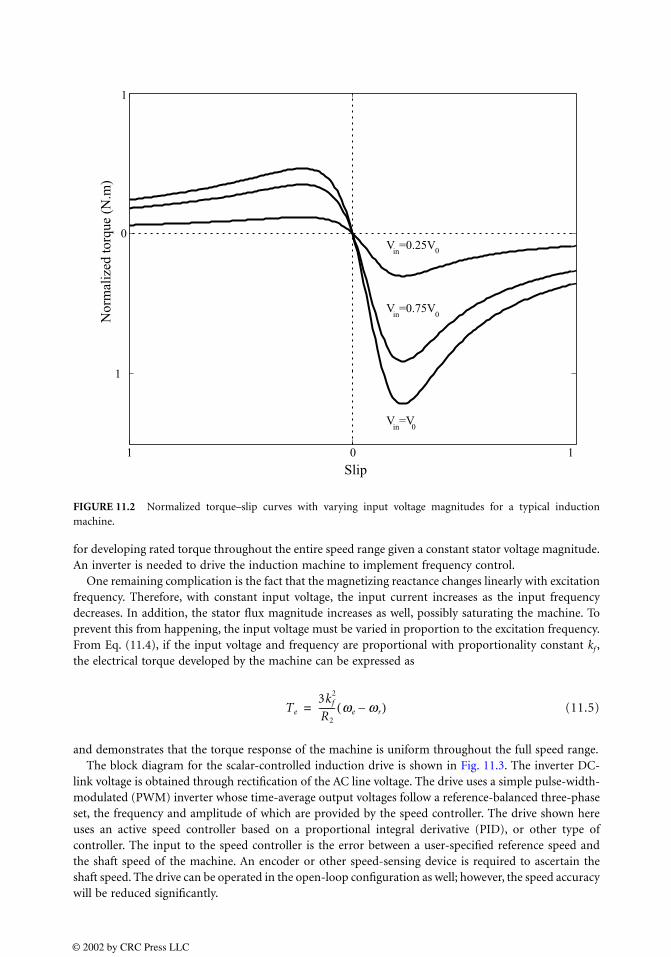
for developing rated torque throughout the entire speed range given a constant stator voltage magnitude.An inverter is needed to drive the induction machine to implement frequency control.
One remaining complication is the fact that the magnetizing reactance changes linearly with excitationfrequency. Therefore, with constant input voltage, the input current increases as the input frequencydecreases. In addition, the stator flux magnitude increases as well, possibly saturating the machine. Toprevent this from happening, the input voltage must be varied in proportion to the excitation frequency.From Eq. (11.4), if the input voltage and frequency are proportional with proportionality constant kf ,the electrical torque developed by the machine can be expressed as
(11.5)
and demonstrates that the torque response of the machine is uniform throughout the full speed range.The block diagram for the scalar-controlled induction drive is shown in Fig. 11.3. The inverter DC-
link voltage is obtained through rectification of the AC line voltage. The drive uses a simple pulse-width-modulated (PWM) inverter whose time-average output voltages follow a reference-balanced three-phaseset, the frequency and amplitude of which are provided by the speed controller. The drive shown hereuses an active speed controller based on a proportional integral derivative (PID), or other type ofcontroller. The input to the speed controller is the error between a user-specified reference speed andthe shaft speed of the machine. An encoder or other speed-sensing device is required to ascertain theshaft speed. The drive can be operated in the open-loop configuration as well; however, the speed accuracywill be reduced significantly.
FIGURE 11.2 Normalized torque–slip curves with varying input voltage magnitudes for a typical inductionmachine.
101
1
0
Slip
Nor
mal
ized
torq
ue (
N.m
)
Vin
=V0
Vin
=0.75V0
Vin
=0.25V0
1
Te
3kf2
R2
------- we wr–( )=
© 2002 by CRC Press LLC
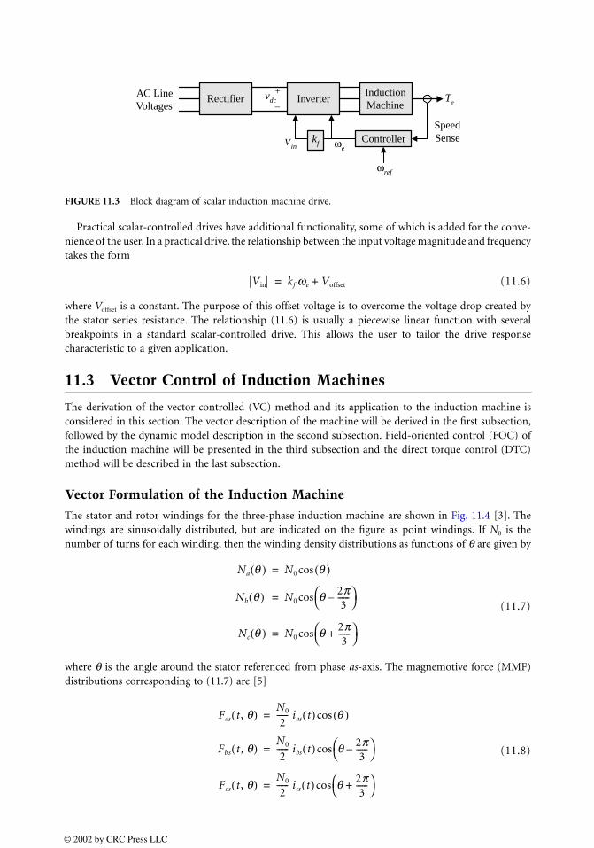
Practical scalar-controlled drives have additional functionality, some of which is added for the conve-nience of the user. In a practical drive, the relationship between the input voltage magnitude and frequencytakes the form
(11.6)
where Voffset is a constant. The purpose of this offset voltage is to overcome the voltage drop created bythe stator series resistance. The relationship (11.6) is usually a piecewise linear function with severalbreakpoints in a standard scalar-controlled drive. This allows the user to tailor the drive responsecharacteristic to a given application.
11.3 Vector Control of Induction Machines
The derivation of the vector-controlled (VC) method and its application to the induction machine isconsidered in this section. The vector description of the machine will be derived in the first subsection,followed by the dynamic model description in the second subsection. Field-oriented control (FOC) ofthe induction machine will be presented in the third subsection and the direct torque control (DTC)method will be described in the last subsection.
Vector Formulation of the Induction Machine
The stator and rotor windings for the three-phase induction machine are shown in Fig. 11.4 [3]. Thewindings are sinusoidally distributed, but are indicated on the figure as point windings. If N0 is thenumber of turns for each winding, then the winding density distributions as functions of θ are given by
(11.7)
where θ is the angle around the stator referenced from phase as-axis. The magnemotive force (MMF)distributions corresponding to (11.7) are [5]
(11.8)
FIGURE 11.3 Block diagram of scalar induction machine drive.
InverterRectifier vdc+_
AC LineVoltages
InductionMachine
Te
Controllerkf
SpeedSenseωe
Vin
ωref
Vin kf we Voffset+=
Na q( ) N0 q( )cos=
Nb q( ) N0 q 2p3
------– cos=
Nc q( ) N0 q 2p3
------+ cos=
Fas t, q( )N0
2------ ias t( ) q( )cos=
Fbs t, q( )N0
2------ ibs t( ) q 2p
3------–
cos=
Fcs t, q( )N0
2------ ics t( ) q 2p
3------+
cos=
© 2002 by CRC Press LLC
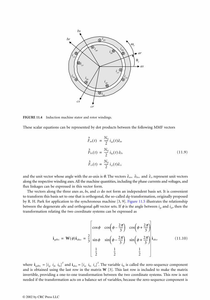
These scalar equations can be represented by dot products between the following MMF vectors
(11.9)
and the unit vector whose angle with the as-axis is θ. The vectors and represent unit vectorsalong the respective winding axes. All the machine quantities, including the phase currents and voltages, andflux linkages can be expressed in this vector form.
The vectors along the three axes as, bs, and cs do not form an independent basis set. It is convenientto transform this basis set to one that is orthogonal, the so-called dq-transformation, originally proposedby R. H. Park for application to the synchronous machine [3, 9]. Figure 11.5 illustrates the relationshipbetween the degenerate abc and orthogonal qd0 vector sets. If φ is the angle between iqs and ias, then thetransformation relating the two coordinate systems can be expressed as
(11.10)
where = [iqs ids i0s]T and iabcs = [ias ibs ics]
T. The variable i0s is called the zero-sequence component
and is obtained using the last row in the matrix W [3]. This last row is included to make the matrixinvertible, providing a one-to-one transformation between the two coordinate systems. This row is notneeded if the transformation acts on a balance set of variables, because the zero-sequence component is
FIGURE 11.4 Induction machine stator and rotor windings.
ias
ibs
ibs
ics
ics
ias
iar
iar
ibr
icr
icr
ibr
θr
ωr
ar
cr
br
as
cs
bs
Fas t( )N0
2------ ias t( ) eas=
Fbs t( )N0
2------ ibs t( ) ebs=
Fcs t( )N0
2------ ics t( ) ecs=
eas, ebs, ecs
iqd0s W f( )iabcs23--
fcos f 2p3
------– cos f 2p
3------+
cos
fsin f 2p3
------– sin f 2p
3------+
sin
12-- 1
2-- 1
2--
iabcs= =
iqd0s
© 2002 by CRC Press LLC

equal to zero. The zero-sequence component carries information about the neutral point of the abcvariables being transformed. If the set is not balanced, this neutral point is not necessarily zero.
The constant multiplying the matrix of (11.10) is, in general, arbitrary. With this constant equal to as it is in (11.10), the result is the power invariant transformation. By using this transformation, thecalculated power in the abc coordinate system is equal to that computed in the qd0 system [3].
If the angle φ = 0, the result is a transformation from the stationary abc system to the stationary qd0system. However, transformation to a reference frame rotating at an arbitrary speed ω is possible bydefining
(11.11)
As will be seen later, the rotor flux–oriented vector control method makes use of this concept, trans-forming the machine variables to the synchronous reference frame where they are constants in steadystate [4].
To understand this concept intuitively, consider the balanced set of stator MMF vectors of a typicalinduction machine given in (11.9). It is not difficult to show that the sum of these vectors produces aresultant MMF vector that rotates at the frequency of the stator currents. The length of the vector isdependent upon the magnitude of the MMF vectors. Observing the system from the synchronousreference frame effectively removes the rotational motion, resulting in only the magnitude of the vectorbeing of consequence. If the magnitudes of the MMF vectors are constant, then the synchronous variableswill be constant. Transients in the magnitudes of the stationary variables result in transients in thesynchronous variables. This is true for currents, voltages, and other variables associated with the machine.
Induction Machine Dynamic Model
The six-state induction machine model in the arbitrary reference frame is presented in this section. Thisdynamic model will be used to derive the FOC and DTC methods. As will be seen, the derivations ofthese control methods will be simpler if they are performed in a specific coordinate reference frame. Anadditional advantage is that transforming to the qd0 coordinate system in any reference frame removes
FIGURE 11.5 Illustration for reference frame transformation.
φ
iqs
iics
ias
bsi
ds
23--
f t( ) w dt0
t
∫=
© 2002 by CRC Press LLC

the time-varying inductances associated with the induction machine [10]. The machine model in a givenreference frame is obtained by substituting the appropriate frequency for ω in the model equations.
The state equations for the six-state induction motor model in the arbitrary reference frame are givenin Eqs. (11.12) through (11.22) [3, 4]. The induction machine nomenclature is provided in Table 11.1.The derivative operator is denoted by p, and the rotor quantities are referred to the stator. The stateequations are
(11.12)
(11.13)
(11.14)
(11.15)
(11.16)
(11.17)
where the stator and rotor flux linkages are given by
(11.18)
(11.19)
(11.20)
(11.21)
TABLE 11.1 Induction Machine Nomenclature
Induction Machine Parameter or Variable Symbol
Stator voltages (V) vqs, vds
Stator currents (A) iqs, ids
Stator flux-linkages (Wb) λqs, λds
Rotor voltages (V) vqr, vdr
Rotor currents (A) iqr, idr
Rotor flux-linkages (Wb) λqr, λdr
Reference frame speed (rad/s) ωRotor speed (rad/s) ωr
Stator series resistance (Ω) rs
Stator leakage inductance (H) Lls
Rotor series resistance (Ω) rr
Rotor leakage inductance (H) Llr
Magnetizing inductance (H) Lm
Number of machine poles PDeveloped electrical torque (N⋅m) Te
Machine load torque (N⋅m) Tload
Torque due to windage and friction losses (N⋅m) Tloss
vqs rsiqs plqs wlds+ +=
vds rsids plds wlqs–+=
vqr 0 rriqr plqr w wr–( )ldr+ += =
vdr 0 rridr pldr w wr–( )lqr–+= =
pwrP2J----- Te Tload– Tloss–( )=
pqr wr=
lds Llsids Lm ids idr+( )+=
lqs Llsiqs Lm iqs iqr+( )+=
ldr Llridr Lm ids idr+( )+=
lqr Llriqr Lm iqs iqr+( )+=
© 2002 by CRC Press LLC

The electrical torque developed by the machine is [4, 5]
(11.22)
where the stator transient reactance is defined as = Ls − where Lr = Llr + Lm and Ls = Lls + Lm.It is important to note that in Eqs. (11.14) and (11.15), the shaft speed ωr is expressed in electricalradians-per-second, that is, scaled by the number of machine pole pairs.
Field-Oriented Control of the Induction Machine
Field-oriented control is probably the most common control method used for high-performance induc-tion machine applications. Rotor flux orientation (RFO) in the synchronous reference frame is consideredhere [4]. There are other orientation possibilities, but rotor flux orientation is the most prominent, andso will be presented in detail.
The RFO control method involves making the induction machine behave similarly to a DC machine.The rotor flux is aligned entirely along the d-axis. The stator currents are split into two components: afield-producing component that induces the rotor flux and a torque-producing component that is orthog-onal to the rotor field. This is analogous to the DC machine where the field flux is along one direction, andthe commutator ensures an orthogonal armature current vector. This task is greatly simplified throughtransformation of the machine variables to the synchronously rotating reference frame.
Under FOC, the q-axis rotor flux linkage is zero in the synchronous reference frame, by using Eq. (11.22),the electric torque of the induction machine can be expressed as
(11.23)
where the e superscript indicates evaluation in the synchronous reference frame. This torque equationis very similar to that of the DC machine. If either the flux linkage or current is held constant,then the torque can be controlled by changing the other. Assuming the inverter driving the inductionmachine is current sourced, the stator currents can be controlled almost instantaneously. However, bysetting = 0 in Eq. (11.15) and substituting the result in Eq. (11.20), it can be shown that the d-axisrotor flux linkage is governed by
(11.24)
where τr is termed the rotor time constant. Equation (11.24) dictates that the rotor flux cannot be changedarbitrarily fast. Therefore, the best dynamic torque response will result if the rotor flux linkage is heldconstant, and the electrical torque is controlled by changing Assuming a current-sourced inverter,this control configuration allows torque control for which the response is limited only by the responsetime of the inverter driving the machine.
Implementation of RFO control requires that the machine variables be transformed to the synchronousreference frame. To accomplish this task, the synchronous reference frame speed must be calculated insome manner. There are two common methods of finding the synchronous speed. In indirect FOC, thesynchronous speed is obtained by using a rotor speed measurement and a corresponding slip calculation[4, 11]. Direct FOC uses air-gap flux measurement or other machine-related quantities to compute thesynchronous speed. The indirect method is the most common and will be presented here.
Te
3PLm
4Lr
------------ ldriqs lqrids–( )3PLm
LrL′s------------ lqsldr lqrlds–( )= =
L′s Lm2 /Lr,
Te
3PLm
4Lr
------------ ldre iqs
e=
ldre iqs
e
lqre
ldre Lmrr
Llr Lm+( )p 1+----------------------------------- ids
e Lm
trp 1+---------------- ids
e= =
iqse .
© 2002 by CRC Press LLC
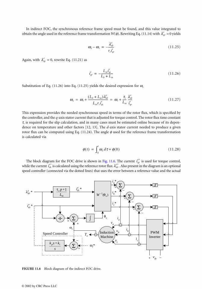
In indirect FOC, the synchronous reference frame speed must be found, and this value integrated toobtain the angle used in the reference frame transformation W(φ). Rewriting Eq. (11.14) with = 0 yields
(11.25)
Again, with = 0, rewrite Eq. (11.21) as
(11.26)
Substitution of Eq. (11.26) into Eq. (11.25) yields the desired expression for ωe
(11.27)
This expression provides the needed synchronous speed in terms of the rotor flux, which is specified bythe controller, and the q-axis stator current that is adjusted for torque control. The rotor flux time constantτr is required for the slip calculation, and in many cases must be estimated online because of its depen-dence on temperature and other factors [12, 13]. The d-axis stator current needed to produce a givenrotor flux can be computed using Eq. (11.24). The angle φ used for the reference frame transformationis calculated via
(11.28)
The block diagram for the FOC drive is shown in Fig. 11.6. The current is used for torque control,while the current is calculated using the reference rotor flux Also present in the diagram is an optionalspeed controller (connected via the dotted lines) that uses the error between a reference value and the actual
FIGURE 11.6 Block diagram of the indirect FOC drive.
lqre
we wr–ldr
e
rriqre
--------–=
lqre
iqre Lmiqs
e
Llr Lm+------------------–=
we wr
Llr Lm+( )ldre
Lmrriqse
------------------------------+ wr
tr
Lm
------ldr
e
iqse
------+= =
f t( ) we dt0
t
∫ f 0( )+=
iqse∗
idse∗ ldr
e∗.
m
r
Lp 1+τ
)(1eW θ-
∫
*edrλ
÷ Σ
Σ
Σ
Σ
PWMInverter
InductionMachine
ωr
Te
ia
ib
ic
ia*
ib*
ic*
*edsi
*eqsi
θe
+
+
+
_
_
_
vc
vb
va
Σ ωr*s
ksk ip +
Speed Controller
vdc+ _
_
++
+
© 2002 by CRC Press LLC
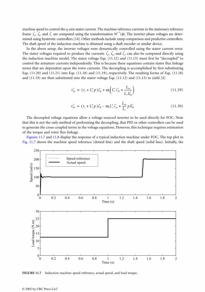
machine speed to control the q-axis stator current. The machine reference currents in the stationary referenceframe , , and are computed using the transformation W
−1(φ). The inverter phase voltages are deter-
mined using hysteretic controllers [14]. Other methods include ramp comparison and predictive controllers.The shaft speed of the induction machine is obtained using a shaft encoder or similar device.
In the above setup, the inverter voltages were dynamically controlled using the stator current error.The stator voltages required to produce the currents , , and , can also be computed directly usingthe induction machine model. The stator voltage Eqs. (11.12) and (11.13) must first be “decoupled” tocontrol the armature currents independently. This is because these equations contain stator flux linkageterms that are dependent upon the rotor currents. The decoupling is accomplished by first substitutingEqs. (11.20) and (11.21) into Eqs. (11.18) and (11.19), respectively. The resulting forms of Eqs. (11.18)and (11.19) are then substituted into the stator voltage Eqs. (11.12) and (11.13) to yield [4]
(11.29)
(11.30)
The decoupled voltage equations allow a voltage-sourced inverter to be used directly for FOC. Notethat this is not the only method of performing the decoupling, that PID or other controllers can be usedto generate the cross-coupled terms in the voltage equations. However, this technique requires estimationof the torque and rotor flux linkage.
Figures 11.7 and 11.8 display the response of a typical induction machine under FOC. The top plot inFig. 11.7 shows the machine speed reference (dotted line) and the shaft speed (solid line). Initially, the
FIGURE 11.7 Induction machine speed reference, actual speed, and load torque.
ia∗ ib
∗ ic∗
ia∗ ib
∗ ic∗
vqse rs L′s p+( )iqs
e we L′s i dse Lm
Lrldre
-----------+ +=
vdse rs L′s p+( )ids
e weL′s i qse Lm
Lr
------ pldre+–=
250
0 0.2 0.4 0.6 0.8 1 1.2 1.4 1.6 1.8 20
50
100
150
200
Time (s)
Spee
d (r
ad/s
)
Speed referenceActual speed
0 0.2 0.4 0.6 0.8 1 1.2 1.4 1.6 1.8 20
5
10
15
20
25
30
Loa
d to
rque
(N
.m)
Time (s)
© 2002 by CRC Press LLC
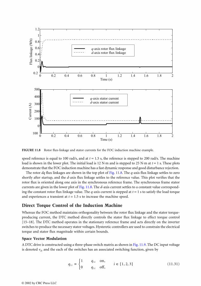
speed reference is equal to 100 rad/s, and at t = 1.5 s, the reference is stepped to 200 rad/s. The machineload is shown in the lower plot. The initial load is 12 N⋅m and is stepped to 25 N⋅m at t = 1 s. These plotsdemonstrate that the FOC induction machine has a fast dynamic response and good disturbance rejection.
The rotor dq flux linkages are shown in the top plot of Fig. 11.8. The q-axis flux linkage settles to zeroshortly after startup, and the d-axis flux linkage settles to the reference value. This plot verifies that therotor flux is oriented along one axis in the synchronous reference frame. The synchronous frame statorcurrents are given in the lower plot of Fig. 11.8. The d-axis current settles to a constant value correspond-ing the constant rotor flux linkage value. The q-axis current is stepped at t = 1 s to satisfy the load torqueand experiences a transient at t = 1.5 s to increase the machine speed.
Direct Torque Control of the Induction Machine
Whereas the FOC method maintains orthogonality between the rotor flux linkage and the stator torque-producing current, the DTC method directly controls the stator flux linkage to effect torque control[15–18]. The DTC method operates in the stationary reference frame and acts directly on the inverterswitches to produce the necessary stator voltages. Hysteretic controllers are used to constrain the electricaltorque and stator flux magnitude within certain bounds.
Space Vector Modulation
A DTC drive is constructed using a three-phase switch matrix as shown in Fig. 11.9. The DC input voltageis denoted vdc and the each of the switches has an associated switching function, given by
(11.31)
FIGURE 11.8 Rotor flux-linkage and stator currents for the FOC induction machine example.
0 0.2 0.4 0.6 0.8 1 1.2 1.4 1.6 1.8 20.2
0
0.2
0.4
0.6
0.8
1
Time (s)
Flux
link
age
(Wb)
q-axis rotor flux linkaged-axis rotor flux linkage
0 0.2 0.4 0.6 0.8 1 1.2 1.4 1.6 1.8 2100
0
100
200
300
400
500
Time (s)
Cur
rent
(A
)
q-axis stator currentd-axis stator current
1.2
q1i
1 q1i on,
0 q1i off,i 1, 2, 3[ ]∈
=
© 2002 by CRC Press LLC
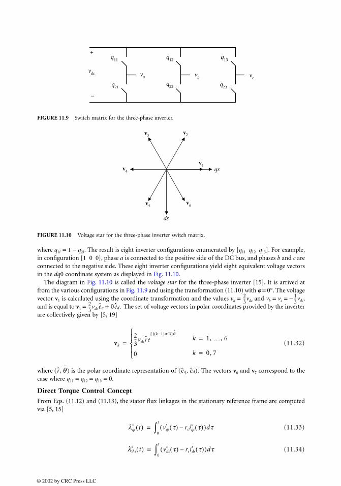
where q1i = 1 − q2i. The result is eight inverter configurations enumerated by [q11 q12 q13]. For example,in configuration [1 0 0], phase a is connected to the positive side of the DC bus, and phases b and c areconnected to the negative side. These eight inverter configurations yield eight equivalent voltage vectorsin the dq0 coordinate system as displayed in Fig. 11.10.
The diagram in Fig. 11.10 is called the voltage star for the three-phase inverter [15]. It is arrived atfrom the various configurations in Fig. 11.9 and using the transformation (11.10) with φ = 0°. The voltagevector v1 is calculated using the coordinate transformation and the values va = vdc and vb = vc = − vdc,and is equal to v1 = vdc The set of voltage vectors in polar coordinates provided by the inverterare collectively given by [5, 19]
(11.32)
where is the polar coordinate representation of The vectors v0 and v7 correspond to thecase where q11 = q12 = q13 = 0.
Direct Torque Control Concept
From Eqs. (11.12) and (11.13), the stator flux linkages in the stationary reference frame are computedvia [5, 15]
(11.33)
(11.34)
FIGURE 11.9 Switch matrix for the three-phase inverter.
FIGURE 11.10 Voltage star for the three-phase inverter switch matrix.
va vb vc
vdc
_
+q11
q21
q12 q13
q22 q23
v1qs
23
v4
v5v6
vv
ds
23-- 1
3--
23-- eq 0 ed.+
vk
23--vdcre
j(k−1)p/3[ ]qˆ
0
=k 1, …, 6=
k 0, 7=
( r, qˆ ) ( eq, ed).
lqss t( ) vqs
s t( ) rsiqss t( )–( )
0
t
∫ dt=
ld ss t( ) vds
s t( ) rsidss t( )–( )
0
t
∫ dt=
© 2002 by CRC Press LLC

where the superscripted s indicates evaluation in the stationary reference frame. If the stator resistancers is small, as is usually the case, the stator flux linkages can be approximated as the time integral of thestator voltages. This approximation coupled with the space vector development above provides the meansfor directly controlling the stator flux linkage vector by manipulation of the stator voltages.
The electrical torque developed by the three-phase induction machine (11.22) can be written as thecross product [3, 4]
(11.35)
where and ρ is the angle between the stator and rotor flux linkages.It is clear from Eq. (11.35), if the stator and rotor flux linkage magnitudes are held constant, then themachine torque can be controlled by changing the angle ρ. The angle ρ cannot be changed directly, butcan be indirectly modified by changing the stator flux linkage angle rapidly. This is because the statorflux time constant is typically much faster than the rotor flux time constant. If the stator flux linkage ischanged quickly, the rotor flux will lag behind, resulting in a change in ρ.
Hysteretic comparators are used to control the inverter switches to adjust the magnitude and angle ofthe stator flux linkage. This is because the voltages cannot be controlled through continuous ranges, onlytwo discrete levels: each phase can only be connected to either the positive or negative DC bus voltage.The two-level hysteretic control function is defined as
(11.36)
The two quantities to be controlled are the electrical torque via the angle ρ, and the stator flux linkagemagnitude. The hysteretic controllers are used to maintain these two quantities within the ranges λref +∆λ ≥ ≥ λref − ∆λ and Tref + ∆T ≥ Te ≥ Tref − ∆T. The comparators provide the necessary inverterswitch configurations to ensure that the torque and stator flux linkage magnitude stay within these limits.A rule set relating the torque and stator flux linkage error to the set of inverter configurations must bedeveloped. To simplify this task, the coordinate frame is separated into sectors as shown in Fig. 11.11.There are six sectors corresponding to the six active inverter states.
To understand why the sectors are used, consider the situation where the stator flux linkage vector isin Sector 1, and its magnitude and angle γ must be increased. If the stator voltage vector v2 is used, theflux linkage magnitude and the angle γ will both increase no matter where the flux linkage vector residesin Sector 1. The vector v1 cannot be reliably used to accomplish this goal, because if the stator flux linkagevector is ahead of v1, the angle γ will decrease, resulting in a torque decrease. All of the appropriatecontroller responses can be worked out this way to form the lookup table shown in Table 11.2 [4]. Giventhe sector number in which the stator flux linkage resides and the outputs of the flux linkage magnitudeand torque hysteretic comparators, the table provides the required inverter voltage vector. The flux linkagecomparator is two level, and the torque comparator is three level. If the estimated torque is within the specifiedbounds of the comparator, a zero voltage vector is selected. In this case, the zero voltage vector that requiresthe fewest inverter switches changing state is used.
To implement the control described above, the sector number must be determined. The most straight-forward way of accomplishing this is to find the stator flux linkage angle γ trigonometrically:
(11.37)
Te
3PLm
4L′m------------ λλλλs
s λλλλrs×
3PLm
4L′m------------ λλλλs
s λλλλrs r( )sin= =
λλλλss lds
s lqss[ ]T
= , λλλλrs ldr
s lqrs[ ]T
= ,
g t, x, e, X0( )G1
g t( )G2
x t( ) X0 e+>X0 e x t( ) X0 e–≥ ≥+
x t( ) X0 e–<
=
λλλλss
g tan 1– lsqs
lsds
------
=
© 2002 by CRC Press LLC
Given the flux linkage angle, the sector number is easily found. In practice, this method is not usedbecause of the computational burden that the trigonometric inverse places upon the controller. Practicalcontrollers rely on the sig ns of the flux linkage components to determine the sector number.
One of the major disadvantages of the DTC method is the required accurate estimation of the statorflux linkage and the developed electrical torque. The stator flux linkage is estimated using Eqs. (11.33)and (11.34) with, perhaps, current feedback for correction. The torque is usually estimated using
(11.38)
There are several variants, but these are the most common ways of performing the estimates. The speedof the estimates must be quite fast, with common values for the sampling time in the neighborhood of25 µs [15]. If the sampling time is not fast enough, excursion outside the limits imposed by the torqueand flux comparators will occur.
The block diagram of the DTC induction machine drive is shown in Fig. 11.12. The error betweenthe reference torque and the estimated torque is fed to a three-level hysteretic comparator, and the speederror is g iven to a two-level comparator. The outputs of the comparators are supplied to a vector lookuptable that makes uses o f the relationships in Table 11.2. The optimal switch states are supplied to thePWM inverter that drives the induction machine. The machine torque, stator flux vector, and stator fluxsector are estimated online from the machine phase b and c voltages and currents.
TABLE 11.2 Optimum Lookup Table for DTC Inverter Control
Te Sector 1 Sector 2 Sector 3 Sector 4 Sector 5 Sector 6
Increase Increase v2 v3 v4 v5 v6 v1
Increase Within limits v7 v0 v7 v0 v7 v0
Increase Decrease v6 v1 v2 v3 v4 v5
Decrease Increase v3 v4 v5 v6 v1 v2
Decrease Within limits v0 v7 v0 v7 v0 v7
Decrease Decrease v5 v6 v1 v2 v3 v4
FIGURE 11.11 Sec tor diagram for the DTC control method.
λλλλss
v1
v2v3
v4
v5v6
Sector 1
Sector 2Sector 3
Sector 4
Sector 5 Sector 6
q
d
Te3P4
------ λλλλss is
s×=
© 2002 by CRC Press LLC
FIGURE 11.12 Block diagram of the DTC induction machine drive.
FIGURE 11.13 Stator flux linkage under DTC.
Σ*eT
*ssλ Σ
SwitchingTable
PWMInverter
vdc+_
InductionMachine
Te
Torque and FluxEstimator
_
_+
+
eT~
ssλ~
Sector
ib
ic
vb
vc
Σ
ωr
s
ksk ip +
Speed Controller
_
+
*
λref
∆ λ
λref
+ ∆ λ
λdss (Wb)
λqss (Wb)
-
© 2002 by CRC Press LLC
FIGURE 11.14 Speed reference, actual shaft speed, and load torque for the DTC drive example.
FIGURE 11.15 The electrical torque for the DTC drive.
0 0.05 0.1 0.15 0.2 0.25 0.30
50
100
150
Time (s)
Spee
d (r
ad/s
)
Speed referenceActual speed
0 0.05 0.1 0.15 0.2 0.25 0.30
5
10
15
20
25
30
Time (s)
Loa
d to
rque
(N
.m)
0 0.05 0.1 0.15 0.2 0.25 0.3100
80
60
40
20
0
20
40
60
80
100
Time (s)
Ele
ctri
cal t
orqu
e (N
.m)
© 2002 by CRC Press LLC
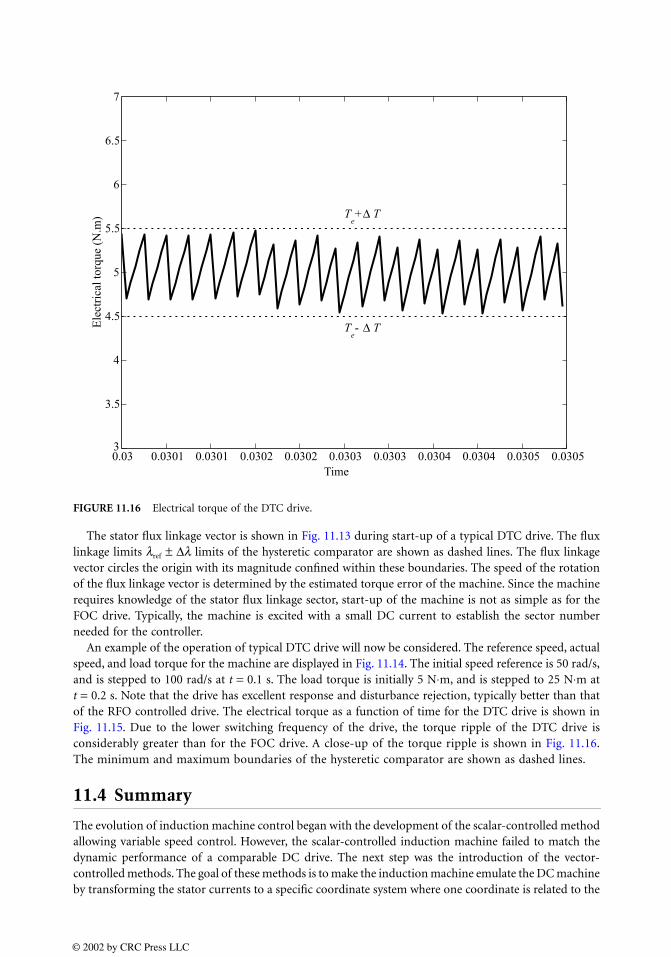
The stator flux linkage vector is shown in Fig. 11.13 during start-up of a typical DTC drive. The fluxlinkage limits λref ± ∆λ limits of the hysteretic comparator are shown as dashed lines. The flux linkagevector circles the origin with its magnitude confined within these boundaries. The speed of the rotationof the flux linkage vector is determined by the estimated torque error of the machine. Since the machinerequires knowledge of the stator flux linkage sector, start-up of the machine is not as simple as for theFOC drive. Typically, the machine is excited with a small DC current to establish the sector numberneeded for the controller.
An example of the operation of typical DTC drive will now be considered. The reference speed, actualspeed, and load torque for the machine are displayed in Fig. 11.14. The initial speed reference is 50 rad/s,and is stepped to 100 rad/s at t = 0.1 s. The load torque is initially 5 N⋅m, and is stepped to 25 N⋅m att = 0.2 s. Note that the drive has excellent response and disturbance rejection, typically better than thatof the RFO controlled drive. The electrical torque as a function of time for the DTC drive is shown inFig. 11.15. Due to the lower switching frequency of the drive, the torque ripple of the DTC drive isconsiderably greater than for the FOC drive. A close-up of the torque ripple is shown in Fig. 11.16.The minimum and maximum boundaries of the hysteretic comparator are shown as dashed lines.
11.4 Summary
The evolution of induction machine control began with the development of the scalar-controlled methodallowing variable speed control. However, the scalar-controlled induction machine failed to match thedynamic performance of a comparable DC drive. The next step was the introduction of the vector-controlled methods. The goal of these methods is to make the induction machine emulate the DC machineby transforming the stator currents to a specific coordinate system where one coordinate is related to the
FIGURE 11.16 Electrical torque of the DTC drive.
0.03 0.0301 0.0301 0.0302 0.0302 0.0303 0.0303 0.0304 0.0304 0.0305 0.03053
3.5
4
4.5
5
5.5
6
6.5
Ele
ctri
cal t
orqu
e (N
.m) T
e+∆ T
Te- ∆ T
Time
7
© 2002 by CRC Press LLC
torque production and the other to rotor flux. The FOC methods provide excellent dynamic response,matching that of the DC machine. The main disadvantage of such controls is the computational overheadrequired in the coordinate transformation.
The latest development in induction machine control is the DTC method. DTC does not rely oncoordinate transformation, but rather controls the stator flux linkage in the stationary reference frame.Despite its control simplicity, the DTC method provides possibly the best dynamic response of any ofthe methods. The average switching frequency of the drive is lower as well, reducing switching loss ascompared with the FOC drive. Since the control basis is the stator flux linkage, the DTC drive is capableof advanced functions such as performing “flying starts” and flux braking [15, 18]. Its main disadvantagelies in the need for accurate estimation of the machine electrical torque and stator flux linkage. At lowspeeds, loss of flux control can occur [20]. An additional drawback of the DTC drive is a greater torqueripple stemming from the low switching frequency.
Both drive types rely on knowledge of the machine parameters for control and observation; therefore,initial commissioning is usually required by both the FOC and DTC drives before start-up. The goal ofthe commissioning stage is to use low-level excitation to obtain estimates of the machine parameters.After the commissioning stage, and during normal operation, online parameter estimation is typicallyemployed.
References
1. V. Del Toro, Basic Electric Machines, Prentice-Hall, Englewood Cliffs, NJ, 1990.2. G. K. Dubey, Power Semiconductor Controlled Drives, Prentice-Hall, Englewood Cliffs, NJ, 1989.3. P. C. Krause, O. Wasynczuk, and S. D. Sudhoff, Analysis of Electric Machinery, IEEE Press, New York,
1995.4. D. W. Novotny and T. A. Lipo, Vector Control and Dynamics of AC Drives, Oxford University Press,
New York, 1996.5. P. Vas, Sensorless Vector and Direct Torque Control, Oxford University Press, New York, 1998.6. T. Lipo, Recent progress in the development of solid-state AC motor drives, IEEE Trans. Power
Electron., 3(2), 105–117, April 1988.7. W. Leonhard, Adjustable-speed AC drives, Proc. IEEE, 76(4), 455–471, April 1988.8. G. O. Garcia, R. M. Stephan, and E. H. Watanabe, Comparing the indirect field-oriented control
with a scalar method, IEEE Trans. Ind. Appl., 41(2), 201–207, April 1994.9. R. H. Park, Two-reaction theory of synchronous machines: generalized method of analysis-part I,
AIEE Trans., 48, 716–730, 1929.10. H. C. Stanley, An analysis of the induction machine, AIEE Trans., 57, 751–755, 1938.11. N. P. Rubin, R. G. Harley, and G. Diana, Evaluation of various slip estimation techniques for an
induction machine operating under field-oriented control conditions, IEEE Trans. Ind. Appl., 28(6),1367–1375, December 1992.
12. W. Leonhard, Control of Electrical Drives, Springer-Verlag, New York, 1996.13. J. C. Moreira and T. A. Lipo, A new method for rotor time constant tuning in indirect field oriented
control, in Power Electronics Spec. Conf., 573–580, 1990.14. D. M. Brod and D. W. Novotny, Current control of VSI-PWM inverters, IEEE Trans. Ind. Appl., IA-
21(4), 562–570, 1985.15. P. Tiitinen, P. Pohjalainen, and J. Lalu, The next generation motor control method: direct torque
control, DTC, in Proc. EPE Chapter Symp. Electric Drive Design Appl., 1–7, October 1994.16. M. Depenbrock, Direct self-control (DSC) of inverter fed induction machine, IEEE Trans. Power
Electron, 3(4), 420–429, 1988.17. J. Kang and S. Sul, New direct torque control of induction motor for minimum torque ripple and
constant switching frequency, IEEE Trans. Ind. Appl., 35(5), 1076–1081, 1999.
© 2002 by CRC Press LLC

18. J. N. Nash, Direct torque control, induction motor vector control without an encoder, IEEE Trans.Ind. Appl., 33(2), 333–341, 1997.
19. T. G. Habetler, F. Profumo, M. Pastorelli, and L. M. Tolbert, Direct torque control of inductionmachines using space vector modulation, IEEE Trans. Ind. Appl., 28(5), 1045–1053, 1992.
20. D. Telford, M. W. Dunnigan, and B. W. Williams, A comparison of vector control and direct torquecontrol of an induction machine, in Power Electronics Spec. Conf., 1, 421–426, 2000.
© 2002 by CRC Press LLC
12Permanent-Magnet
SynchronousMachine Drives
12.1 Introduction12.2 Construction of PMSM Drive Systems12.3 Simulation and Model12.4 Controlling the PMSM
Current-Based Drives • Voltage-Based Drives
12.5 Advanced Topics in PMSM Drives
12.1 Introduction
The permanent-magnet synchronous machine (PMSM) drive has emerged as a top competitor for a fullrange of motion control applications [1–3]. For example, the PMSM is widely used in machine tools,robotics, actuators, and is being considered in high-power applications such as vehicular propulsion andindustrial drives. It is also becoming viable for commercial/residential applications. The PMSM is knownfor having high efficiency, low torque ripple, superior dynamic performance, and high power density.These drives often are the best choice for high-performance applications and are expected to see expandeduse as manufacturing costs decrease. The purpose of this chapter is to introduce the PMSM and theapplication of power electronics technology to its control.
The PMSM is sometimes referred to as a permanent-magnet AC (PMAC) machine or simply as a PMmachine. In some instances it is referred to as a brushless DC (BDC) machine because by appropriatecontrol it can be made to have input/output characteristics much like a separately excited brush-typeDC machine. It can also take on similarity with the DC machine when Hall effect sensors are utilizedfor position sensing, whereby electronic, instead of brush, commutation take place. The BDC machine,which is discussed in detail in Chapter 10, is a special case of the more general PMSM drive. The PMSMis a synchronous machine in the sense that it has a multiphase stator and the stator electrical frequencyis directly proportional to the rotor speed in the steady state. However, it differs from a traditionalsynchronous machine in that it has permanent magnets in place of the field winding and otherwise hasno rotor conductors.
The use of permanent magnets in the rotor facilitates efficiency, eliminates the need for slip rings, andeliminates the electrical rotor dynamics that complicate control (particularly vector control). The per-manent magnets have the drawback of adding significant capital cost to the drive, although the long-term cost can be less through improved efficiency. The PMSM also has the drawback of requiring rotorposition feedback by either direct means or by a suitable estimation system. Since many other high-performance drives utilize position feedback, this is not necessarily a disadvantage. Another disadvanta-geous aspect of the PMSM is cogging torque, which is the parasitic tendency of the rotor to align at
Patrick L. Chapman University of Illinois at Urbana-Champaign
© 2002 by CRC Press LLC
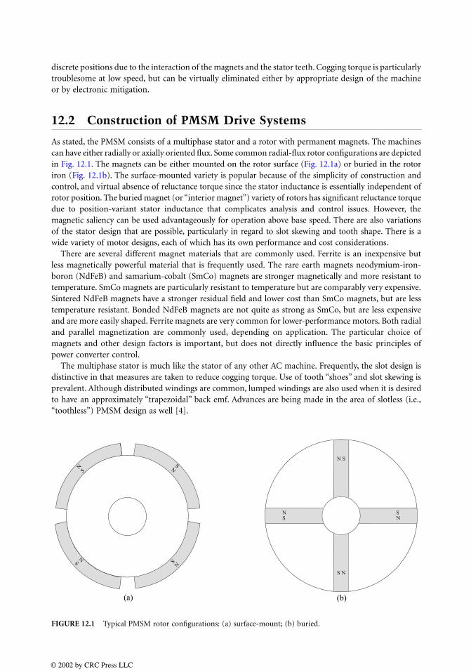
discrete positions due to the interaction of the magnets and the stator teeth. Cogging torque is particularlytroublesome at low speed, but can be virtually eliminated either by appropriate design of the machineor by electronic mitigation.
12.2 Construction of PMSM Drive Systems
As stated, the PMSM consists of a multiphase stator and a rotor with permanent magnets. The machinescan have either radially or axially oriented flux. Some common radial-flux rotor configurations are depictedin Fig. 12.1. The magnets can be either mounted on the rotor surface (Fig. 12.1a) or buried in the rotoriron (Fig. 12.1b). The surface-mounted variety is popular because of the simplicity of construction andcontrol, and virtual absence of reluctance torque since the stator inductance is essentially independent ofrotor position. The buried magnet (or “interior magnet”) variety of rotors has significant reluctance torquedue to position-variant stator inductance that complicates analysis and control issues. However, themagnetic saliency can be used advantageously for operation above base speed. There are also variationsof the stator design that are possible, particularly in regard to slot skewing and tooth shape. There is awide variety of motor designs, each of which has its own performance and cost considerations.
There are several different magnet materials that are commonly used. Ferrite is an inexpensive butless magnetically powerful material that is frequently used. The rare earth magnets neodymium-iron-boron (NdFeB) and samarium-cobalt (SmCo) magnets are stronger magnetically and more resistant totemperature. SmCo magnets are particularly resistant to temperature but are comparably very expensive.Sintered NdFeB magnets have a stronger residual field and lower cost than SmCo magnets, but are lesstemperature resistant. Bonded NdFeB magnets are not quite as strong as SmCo, but are less expensiveand are more easily shaped. Ferrite magnets are very common for lower-performance motors. Both radialand parallel magnetization are commonly used, depending on application. The particular choice ofmagnets and other design factors is important, but does not directly influence the basic principles ofpower converter control.
The multiphase stator is much like the stator of any other AC machine. Frequently, the slot design isdistinctive in that measures are taken to reduce cogging torque. Use of tooth “shoes” and slot skewing isprevalent. Although distributed windings are common, lumped windings are also used when it is desiredto have an approximately “trapezoidal” back emf. Advances are being made in the area of slotless (i.e.,“toothless”) PMSM design as well [4].
FIGURE 12.1 Typical PMSM rotor configurations: (a) surface-mount; (b) buried.
© 2002 by CRC Press LLC
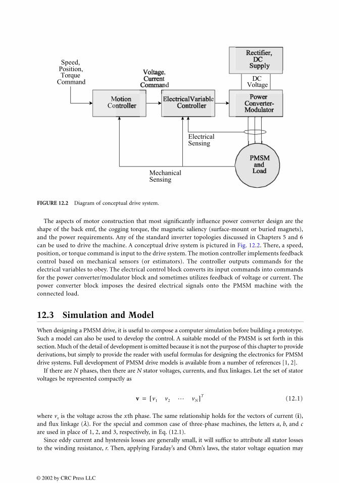
The aspects of motor construction that most significantly influence power converter design are theshape of the back emf, the cogging torque, the magnetic saliency (surface-mount or buried magnets),and the power requirements. Any of the standard inverter topologies discussed in Chapters 5 and 6can be used to drive the machine. A conceptual drive system is pictured in Fig. 12.2. There, a speed,position, or torque command is input to the drive system. The motion controller implements feedbackcontrol based on mechanical sensors (or estimators). The controller outputs commands for theelectrical variables to obey. The electrical control block converts its input commands into commandsfor the power converter/modulator block and sometimes utilizes feedback of voltage or current. Thepower converter block imposes the desired electrical signals onto the PMSM machine with theconnected load.
12.3 Simulation and Model
When designing a PMSM drive, it is useful to compose a computer simulation before building a prototype.Such a model can also be used to develop the control. A suitable model of the PMSM is set forth in thissection. Much of the detail of development is omitted because it is not the purpose of this chapter to providederivations, but simply to provide the reader with useful formulas for designing the electronics for PMSMdrive systems. Full development of PMSM drive models is available from a number of references [1, 2].
If there are N phases, then there are N stator voltages, currents, and flux linkages. Let the set of statorvoltages be represented compactly as
(12.1)
where vx is the voltage across the xth phase. The same relationship holds for the vectors of current (i),and flux linkage (λ). For the special and common case of three-phase machines, the letters a, b, and care used in place of 1, 2, and 3, respectively, in Eq. (12.1).
Since eddy current and hysteresis losses are generally small, it will suffice to attribute all stator lossesto the winding resistance, r. Then, applying Faraday’s and Ohm’s laws, the stator voltage equation may
FIGURE 12.2 Diagram of conceptual drive system.
v v1 v2… vN[ ]T=
© 2002 by CRC Press LLC

be written as
(12.2)
Regarding the machine as balanced, symmetrical, and magnetically linear, the flux linkage equationmay be written as
(12.3)
where L is a symmetric N × N matrix of the appropriate self- and mutual inductances and λpm is anN × 1 vector of stator flux linkages due to the permanent magnet. The inductance matrix is constant formachines with surface-mounted magnets, but has rotor position–dependent terms for machines withburied magnets.
The torque equation can be derived from coenergy relationships:
(12.4)
where θr is the electrical rotor position in radians, and P is the number of poles. Mechanical rotor positionis θrm = 2θr/P. The cogging torque is represented as Tcog.
Equations (12.2) to (12.4) represent a simulation model of the machine, provided that the resistance,r, the inductance matrix, L, the cogging torque, Tcog, and the permanent magnet flux linkage vector, λpm,are known. The parameters can be determined from direct measurement or by calculation from motorgeometry (i.e., finite-element analysis). The mechanical dynamics of the system, which are not discussedhere since they can widely vary, must be simulated to determine position and speed.
The model set forth is general for any number of phases and for the buried or surface-mounted magnetcases. For a surface-mounted magnet machine, the air gap is effectively very wide and uniform since themagnet material has a relative permeability near 1. This results in stator inductance, which is generallynot dependent upon rotor position. In both the surface-mount and buried magnet cases, λpm is a functionof rotor position. Therefore, the torque equation for the surface-mounted case is
(12.5)
and the torque equation for a machine with buried magnets is
(12.6)
where it is noted that the current, i, is not explicitly dependent on rotor position.The cogging torque may be represented as
(12.7)
where Z is the set of natural numbers such that the Fourier series constants and are negligibleand the constant, Nt, is the number of stator teeth. The cogging torque is frequently ignored in designingthe motor drive electronics or it is sufficiently negligible because of special machine design efforts. Ifcogging torque is neglected, then the constants and are zero.
v riddt----- l+=
l Li lpm+=
TeP2--- ∂
∂qr
------- 12-- iTLi iTlpm+
Tcog+=
Te SM( )P2--- iT ∂
∂qr
------- lpm Tcog+=
Te BM( )P2--- iT 1
2-- ∂
∂qr
------- L i
∂∂qr
------- lpm+ Tcog+=
Tcog Tqz zNtqr( ) Td
z zNtqr( )sin+cosz∈Z∑=
Tqz Td
z
Tqz Td
z
© 2002 by CRC Press LLC

The power into the machine is simply the sum of the power into each phase:
(12.8)
and the power output of the machine is
(12.9)
where ω rm is the mechanical rotor speed. In Eq. (12.9), the frictional and windage dynamics are assumedto be negligible or to be accounted for in the mechanical system model.
As a common special case of the model in Eq. (12.9), the analysis is restricted to three-phase machines(N = 3). Frequently, the back emf of the machine has negligible harmonics, and thus it can be treated asif it is purely sinusoidal. As is common in buried magnet machine analysis, the rotor position varianceof the stator inductance can be taken as sinusoidal. Furthermore, the cogging torque can be made smallby utilizing certain design techniques. With these assumptions, a transformation of machine variablesinto the rotor reference frame can be made that facilitates vector control of the PMSM.
If the back emf is sinusoidal, then the flux linkage due the permanent magnets is as well. That is, λpm
may be expressed as
(12.10)
where λm is a constant equal to the peak strength of the flux linkage due to the magnets. Note thatEq. (12.10) implies a certain interpretation of the measured rotor position. Specifically, it implies thatthe magnet flux linking the first phase is zero when θr = 0. Then, the back emf due to the permanentmagnets may be stated as
(12.11)
where ωr is the electrical rotor speed and equals P/2 times its mechanical counterpart, ωrm. Equation (12.11)is a useful expression for determining the constant λm experimentally.
The rotor position–dependent terms can be eliminated by transforming the variables into a referenceframe fixed in the rotor. Only the results of this long process are given here. The transformation is appliedas
(12.12)
where
(12.13)
and [Ref. 1]
(12.14)
Pin vTi=
Pout Tewrm=
lpm lm qr( ) qr2p3
------– qr
2p3
------+ sinsinsin
T
=
epm wrlm qr( )cos qr2p3
------– qr
2p3
------+ coscos
T
=
vqd0 Kv=
vqd0 vq vd v0[ ]T=
K23--
qr( )cos qr2p3
------– cos qr
2p3
------+ cos
qr( )sin qr2p3
------– sin qr
2p3
------+ sin
12-- 1
2-- 1
2--
=
© 2002 by CRC Press LLC
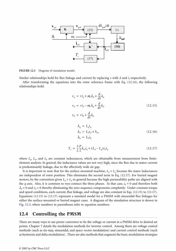
Similar relationships hold for flux linkage and current by replacing v with λ and i, respectively.After transforming the equations into the rotor reference frame with Eq. (12.14), the following
relationships hold:
(12.15)
(12.16)
(12.17)
where Lq, Ld, and L0 are constant inductances, which are obtainable from measurement from finite-element analysis. In general, the inductance values are not very high, since the flux due to stator currentis predominantly leakage, due to the effectively wide air gap.
It is important to note that for the surface-mounted machine, Ld = Lq because the stator inductancesare independent of rotor position. This eliminates the second term in Eq. (12.17). For buried magnetmotors, by the convention given Lq > Ld in general because the high-permeability paths are aligned withthe q-axis. Also, it is common to wye-connect the three phases. In that case, i0 = 0 and therefore bothλ0 = 0 and v0 = 0 thereby eliminating the zero-sequence components completely. Under constant torqueand speed conditions, each current, flux linkage, and voltage are also constant in Eqs. (12.15) to (12.17).Equations (12.15) to (12.17) represent a standard model for a PMSM with sinusoidal flux linkages foreither the surface-mounted or buried magnet cases. A diagram of the simulation structure is shown inFig. 12.3, where numbers in parentheses refer to equation numbers.
12.4 Controlling the PMSM
There are many ways to use power converters to fix the voltage or current in a PMSM drive to desired setpoints. Chapter 7 details the modulation methods for inverter control. Among them are voltage controlmethods (such as six-step, sinusoidal, and space-vector modulation) and current control methods (suchas hysteresis and delta modulation). There are also methods that augment the basic modulation strategies
FIGURE 12.3 Diagram of simulation model.
vq riq wrldddt-----lq+ +=
vd rid wrlqddt-----ld+–=
v0 ri0ddt-----l0+=
lq Lqiq=ld Ldid λm+=l0 L0i0=
Te32-- P
2---lmiq Ld Lq–( )idiq+=
© 2002 by CRC Press LLC
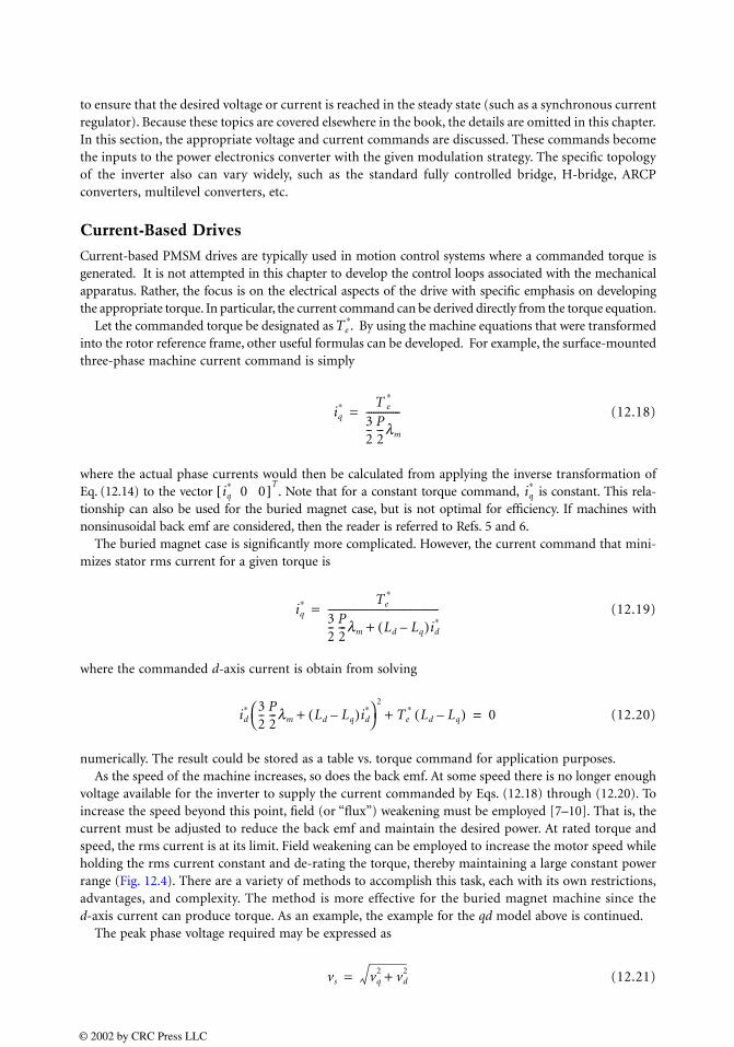
to ensure that the desired voltage or current is reached in the steady state (such as a synchronous currentregulator). Because these topics are covered elsewhere in the book, the details are omitted in this chapter.In this section, the appropriate voltage and current commands are discussed. These commands becomethe inputs to the power electronics converter with the given modulation strategy. The specific topologyof the inverter also can vary widely, such as the standard fully controlled bridge, H-bridge, ARCPconverters, multilevel converters, etc.
Current-Based Drives
Current-based PMSM drives are typically used in motion control systems where a commanded torque isgenerated. It is not attempted in this chapter to develop the control loops associated with the mechanicalapparatus. Rather, the focus is on the electrical aspects of the drive with specific emphasis on developingthe appropriate torque. In particular, the current command can be derived directly from the torque equation.
Let the commanded torque be designated as . By using the machine equations that were transformedinto the rotor reference frame, other useful formulas can be developed. For example, the surface-mountedthree-phase machine current command is simply
(12.18)
where the actual phase currents would then be calculated from applying the inverse transformation ofEq. (12.14) to the vector . Note that for a constant torque command, is constant. This rela-tionship can also be used for the buried magnet case, but is not optimal for efficiency. If machines withnonsinusoidal back emf are considered, then the reader is referred to Refs. 5 and 6.
The buried magnet case is significantly more complicated. However, the current command that mini-mizes stator rms current for a given torque is
(12.19)
where the commanded d-axis current is obtain from solving
(12.20)
numerically. The result could be stored as a table vs. torque command for application purposes. As the speed of the machine increases, so does the back emf. At some speed there is no longer enough
voltage available for the inverter to supply the current commanded by Eqs. (12.18) through (12.20). Toincrease the speed beyond this point, field (or “flux”) weakening must be employed [7–10]. That is, thecurrent must be adjusted to reduce the back emf and maintain the desired power. At rated torque andspeed, the rms current is at its limit. Field weakening can be employed to increase the motor speed whileholding the rms current constant and de-rating the torque, thereby maintaining a large constant powerrange (Fig. 12.4). There are a variety of methods to accomplish this task, each with its own restrictions,advantages, and complexity. The method is more effective for the buried magnet machine since thed-axis current can produce torque. As an example, the example for the qd model above is continued.
The peak phase voltage required may be expressed as
(12.21)
Te∗
iq∗ T e
∗
32-- P
2---lm
--------------=
iq∗ 0 0[ ]T
iq∗
iq∗ Te
∗
32-- P
2---lm Ld Lq–( )id
∗+----------------------------------------------=
id∗ 3
2-- P
2---lm Ld Lq–( )id
∗+
2
Te∗ Ld Lq–( )+ 0=
vs vq2 vd
2+=
© 2002 by CRC Press LLC
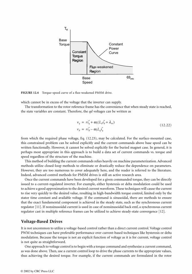
which cannot be in excess of the voltage that the inverter can supply. The transformation to the rotor reference frame has the convenience that when steady state is reached,
the state variables are constant. Therefore, the qd voltages can be written as
(12.22)
from which the required phase voltage, Eq. (12.23), may be calculated. For the surface-mounted case,this constrained problem can be solved explicitly and the current commands above base speed can bewritten functionally. However, it cannot be solved explicitly for the buried magnet case. In general, it isperhaps most appropriate in this approach is to build a data set of current commands vs. torque andspeed regardless of the structure of the machine.
This method of building the current commands relies heavily on machine parameterization. Advancedmethods utilize closed-loop methods to eliminate or drastically reduce the dependence on parameters.However, they are too numerous to cover adequately here, and the reader is referred to the literature.Indeed, advanced control methods for PMSM drives is still an active research area.
Once the current commands have been developed for a given commanded torque, they can be directlyissued to a current-regulated inverter. For example, either hysteresis or delta modulation could be usedto achieve a good approximation to the desired current waveform. These techniques will cause the currentto rise very quickly to the desired value, resulting in high-bandwidth torque control, limited only by thestator time constant and available voltage. If the command is sinusoidal, there are methods to ensurethat the exact fundamental component is achieved in the steady state, such as the synchronous currentregulator [11]. If nonsinusoidal current is used in case of nonsinusoidal back emf, a synchronous currentregulator cast in multiple reference frames can be utilized to achieve steady-state convergence [12].
Voltage-Based Drives
It is not uncommon to utilize a voltage-based control rather than a direct current control. Voltage controlPWM techniques can have preferable performance over current-based techniques like hysteresis or deltamodulation. Because the torque is not an explicit function of voltage as it is for current, voltage controlis not quite as straightforward.
One approach to voltage control is to begin with a torque command and synthesize a current command,as was done above. Then, use a current control loop to drive the phase currents to the appropriate values,thus achieving the desired torque. For example, if the current commands are formulated in the rotor
FIGURE 12.4 Torque–speed curve of a flux-weakened PMSM drive.
vq riq∗ wr Ldid
∗ lm+( )+ =
vd rid∗ wrLqiq
∗–=
© 2002 by CRC Press LLC
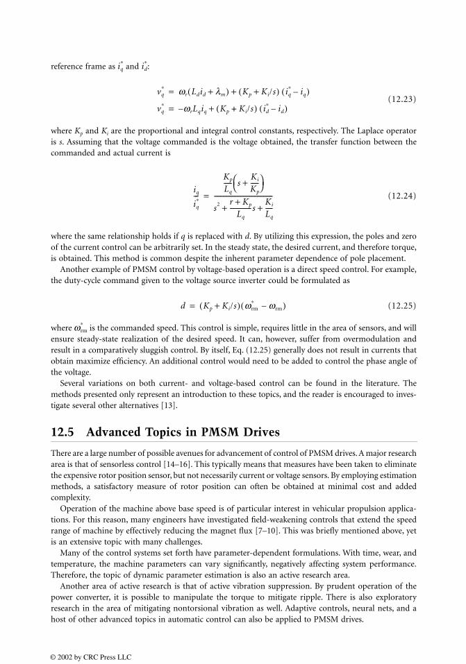
reference frame as and :
(12.23)
where Kp and Ki are the proportional and integral control constants, respectively. The Laplace operatoris s. Assuming that the voltage commanded is the voltage obtained, the transfer function between thecommanded and actual current is
(12.24)
where the same relationship holds if q is replaced with d. By utilizing this expression, the poles and zeroof the current control can be arbitrarily set. In the steady state, the desired current, and therefore torque,is obtained. This method is common despite the inherent parameter dependence of pole placement.
Another example of PMSM control by voltage-based operation is a direct speed control. For example,the duty-cycle command given to the voltage source inverter could be formulated as
(12.25)
where is the commanded speed. This control is simple, requires little in the area of sensors, and willensure steady-state realization of the desired speed. It can, however, suffer from overmodulation andresult in a comparatively sluggish control. By itself, Eq. (12.25) generally does not result in currents thatobtain maximize efficiency. An additional control would need to be added to control the phase angle ofthe voltage.
Several variations on both current- and voltage-based control can be found in the literature. Themethods presented only represent an introduction to these topics, and the reader is encouraged to inves-tigate several other alternatives [13].
12.5 Advanced Topics in PMSM Drives
There are a large number of possible avenues for advancement of control of PMSM drives. A major researcharea is that of sensorless control [14–16]. This typically means that measures have been taken to eliminatethe expensive rotor position sensor, but not necessarily current or voltage sensors. By employing estimationmethods, a satisfactory measure of rotor position can often be obtained at minimal cost and addedcomplexity.
Operation of the machine above base speed is of particular interest in vehicular propulsion applica-tions. For this reason, many engineers have investigated field-weakening controls that extend the speedrange of machine by effectively reducing the magnet flux [7–10]. This was briefly mentioned above, yetis an extensive topic with many challenges.
Many of the control systems set forth have parameter-dependent formulations. With time, wear, andtemperature, the machine parameters can vary significantly, negatively affecting system performance.Therefore, the topic of dynamic parameter estimation is also an active research area.
Another area of active research is that of active vibration suppression. By prudent operation of thepower converter, it is possible to manipulate the torque to mitigate ripple. There is also exploratoryresearch in the area of mitigating nontorsional vibration as well. Adaptive controls, neural nets, and ahost of other advanced topics in automatic control can also be applied to PMSM drives.
iq∗ id
∗
vq∗ wr Ldid lm+( ) Kp Ki/s+( )+ iq
∗ iq–( )=
vq∗ w– rLqiq Kp Ki/s+( )+ id
∗ id–( )=
iq
iq∗---
Kp
Lq
----- sKi
Kp
-----+
s2 r K+ p
Lq
--------------sKi
Lq
-----+ +--------------------------------------=
d Kp Ki/s+( ) wrm ∗ wrm–( )=
wrm∗
© 2002 by CRC Press LLC

In short, the PMSM motor drive is a effective in high-performance drive applications. Rapid torqueresponse is readily achieved as vector control of PMSM drives is much more straightforward than it isfor induction motor drives. The capital cost can be high, but the high efficiency can at least partiallyoffset this in high-power applications. For these reasons, the PMSM drive is expected to continue to becompetitive for the near future.
References
1. P. C. Krause, O. Wasynczuk, and S. D. Sudhoff, Analysis of Electric Machinery, IEEE Press, Piscataway,NJ, 1996.
2. P. Pillay and R. Krishnan, Modeling of permanent magnet motor drives, IEEE Trans. Ind. Electron.,35(4), 537–541, 1988.
3. B. K. Bose, Ed., Power Electronics and Variable Frequency Drives, IEEE Press, Piscataway, NJ, 1997,chap. 6.
4. D. C. Hanselman, Brushless Permanent-Magnet Motor Design, McGraw-Hill, New York, 1994.5. P. L. Chapman, S. D. Sudhoff, and C. A. Whitcomb, Optimal current control strategies for surface-
mounted permanent-magnet synchronous machine drives, IEEE Trans. Energy Conversion, 14(4),1043–1050, 1999.
6. D. C. Hanselman, Minimum torque ripple, maximum efficiency excitation of brushless permanentmagnet motors, IEEE Trans. Ind. Electron., 41(3), 292–300, 1994.
7. S. D. Sudhoff, K. A. Corzine, and H. J. Hegner, A flux-weakening strategy for current-regulated surface-mounted permanent-magnet machine drives, IEEE Trans. Energy Conversion, 10(3), 431–437, 1995.
8. S. R. Macminn and T. M. Jahns, Control techniques for improved high-speed performance of interiorPM synchronous motor drives, IEEE Trans. Ind. Appl., 27(5), 997–1004, 1991.
9. A. K. Adnanes and T. M. Undeland, Optimum torque performance in PMSM drives above ratedspeed, in Conference Record of the 1991 Industry Applications Society Annual Meeting, 1991, 169–175.
10. M. F. Rahman, L. Zhong, and K. W. Lim, A DSP based instantaneous torque control strategy forinterior permanent magnet synchronous motor drive with wide speed range and reduced torqueripples, in Conference Record of the Thirty-First Annual Industry Applications Society Meeting, 1996,518–524.
11. T. M. Rowan and R. J. Kerkman, A new synchronous current regulator and an analysis of current-regulated drives, IEEE Trans. Ind. Appl., IA-22(4), 678–690, 1986.
12. P. L. Chapman and S. D. Sudhoff, A multiple reference frame synchronous estimator/regulator, IEEETrans. Energy Conversion, 15(2), 197–202, 2000.
13. W. Leohnard, Control of Electric Drives, 2nd ed., Springer-Verlag, New York, 1997.14. K. A. Corzine and S. D. Sudhoff, Hybrid observer for high performance brushless DC motor drives,
IEEE Trans. Energy Conversion, 11(2), 318–323, 1996.15. D. Jung and I. Ha, Low-cost sensorless control of brushless DC motors using a frequency-independent
phase shifter, IEEE Trans. Power Electron., 15(4), 742–752, 2000.16. J. P. Johnson, M. Ehsani, and Y. Guzelgunler, Review of sensorless methods for brushless DC, in
Conference Record of the 1999 Industry Applications Society Annual Meeting, 1999, 143–150.
© 2002 by CRC Press LLC

13Switched Reluctance
Machines
13.1 IntroductionAdvantages • Disadvantages
13.2 SRM Configuration13.3 Basic Principle of Operation
Voltage Balance Equation • Energy Conversion • Torque Production • Torque–Speed Characteristics
13.4 Design13.5 Converter Topologies13.6 Control Strategies
Control Parameters • Advance Angle Calculation •Voltage-Controlled Drive • Current-Controlled Drive • Advanced Control Strategies
13.7 Sensorless Control13.8 Applications
13.1 Introduction
The concept of switched reluctance machines (SRMs) was established as early in 1838 by Davidson andwas used to propel a locomotive on the Glasgow–Edinburgh railway near Falkirk [1]. However, the fullpotential of the motor could not be utilized with the mechanical switches available in those days. Theadvent of fast-acting power semiconductor switches revived the interest in SRMs in the 1970s when ProfessorLawrenson’s group established the fundamental design and operating principles of the machine [2]. Therejuvenated interest of researchers supplemented by the developments of computer-aided electromagneticdesign prompted a tremendous growth in the technology over the next three decades. SRM technologyis now slowly penetrating into the industry with the promise of providing an efficient drive system at alower cost.
Advantages
The SRM possess a few unique features that makes it a vigorous competitor to existing AC and DC motorsin various adjustable-speed drive and servo applications. The advantages of an SRM can be summarizedas follows:
• Machine construction is simple and low-cost because of the absence of rotor winding and per-manent magnets.
• There are no shoot-through faults between the DC buses in the SRM drive converter because eachrotor winding is connected in series with converter switching elements.
Iqbal HusainThe University of Akron
© 2002 by CRC Press LLC

• Bidirectional currents are not necessary, which facilitates the reduction of the number of powerswitches in certain applications.
• The bulk of the losses appear in the stator, which is relatively easier to cool.
• The torque–speed characteristics of the motor can be tailored to the application requirement moreeasily during the design stage than in the case of induction and PM machines.
• The starting torque can be very high without the problem of excessive in-rush current due to itshigher self-inductance.
• The open-circuit voltage and short-circuit current at faults are zero or very small.
• The maximum permissible rotor temperature is higher, since there are no permanent magnets.
• There is a low rotor inertia and a high torque/inertia ratio.
• Extremely high speeds with a wide constant power region are possible.
• There are independent stator phases, which does not prevent drive operation in the case of lossof one or more phases.
Disadvantages
The SRM also comes with a few disadvantages among which torque ripple and acoustic noise are the mostcritical. The double saliency construction and the discrete nature of torque production by the independentphases lead to higher torque ripple compared with other machines. The higher torque ripple also causesthe ripple current in the DC supply to be quite large, necessitating a large filter capacitor. The doublysalient structure of the SRM also causes higher acoustic noise compared with other machines. The mainsource of acoustic noise is the radial magnetic force induced resonant vibration with the circumferentialmode shapes of the stator.
The absence of permanent magnets imposes the burden of excitation on the stator windings andconverter, which increases the converter kVA requirement. Compared with PM brushless machines, the per-unit stator copper losses will be higher, reducing the efficiency and torque per ampere. However, themaximum speed at constant power is not limited by the fixed magnet flux as in the PM machine, and,hence, an extended constant power region of operation is possible in SRMs. The control can be simplerthan the field-oriented control of induction machines, although for torque ripple minimization significantcomputations may be required for an SRM drive.
13.2 SRM Configuration
The SRM is a doubly-salient, singly-excited reluctance machine with independent phase windings on thestator, usually made of magnetic steel laminations. The rotor is a simple stack of laminations, withoutany windings or magnets. The cross-sectional diagrams of a four-phase, 8-6 SRM and a three-phase, 12-8SRM are shown in Fig. 13.1. The three-phase, 12-8 machine is a two-repetition version of the basic 6-4structure within the single stator geometry. The two-repetition machine can alternately be labeled as a4-poles/phase machine, compared with the 6-4 structure with two poles/phase. The stator windings ondiametrically opposite poles are connected either in series or in parallel to form one phase of the motor.When a stator phase is energized, the most adjacent rotor pole-pair is attracted toward the energizedstator to minimize the reluctance of the magnetic path. Therefore, it is possible to develop constant torquein either direction of rotation by energizing consecutive phases in succession.
The aligned position of a phase is defined to be the situation when the stator and rotor poles of thephase are perfectly aligned with each other attaining the minimum reluctance position. The unsaturatedphase inductance is maximum (La) in this position. The phase inductance decreases gradually as the rotorpoles move away from the aligned position in either direction. When the rotor poles are symmetricallymisaligned with the stator poles of a phase, the position is said to be the unaligned position. The phasehas the minimum inductance (Lu) in this position. Although the concept of inductance is not valid fora highly saturating machine like SRM, the unsaturated aligned and unaligned inductances are two keyreference positions for the controller.
© 2002 by CRC Press LLC

Several other combinations of the number of stator and rotor poles exist, such as 10-4, 12-8, etc. A 4-2or a 2-2 configuration is also possible, but they have the disadvantage that, if the stator and rotor poles arealigned exactly, then it would be impossible to develop a starting torque. The configurations with highernumber of stator/rotor pole combinations have less torque ripple and do not have the problem of startingtorque.
FIGURE 13.1 Cross sections of two SR machines: (a) four-phase, 8-6 structure; (b) three-phase, 12-8, two-repetitionstructure.
(b)
(a)
A
D
C
B
A
D
C Bs
Br
9
R0
R1
R2
B
R3
N A
3B
4
5
6
7
8
1
2
A
C
BA
B
C
A
S
C
C
B
S
N
© 2002 by CRC Press LLC
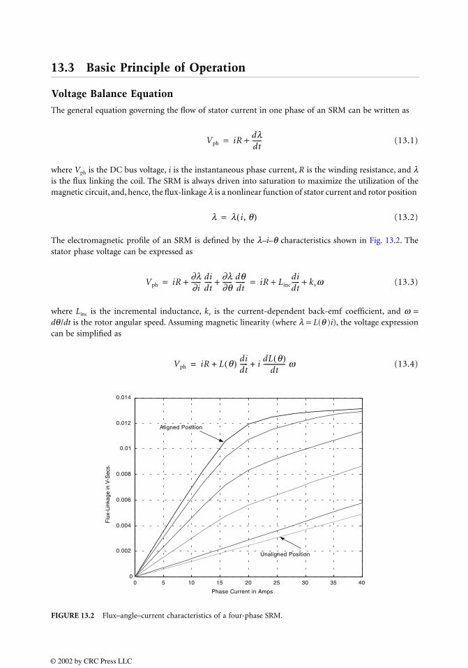
13.3 Basic Principle of Operation
Voltage Balance Equation
The general equation governing the flow of stator current in one phase of an SRM can be written as
(13.1)
where Vph is the DC bus voltage, i is the instantaneous phase current, R is the winding resistance, and λis the flux linking the coil. The SRM is always driven into saturation to maximize the utilization of themagnetic circuit, and, hence, the flux-linkage λ is a nonlinear function of stator current and rotor position
(13.2)
The electromagnetic profile of an SRM is defined by the λ–i–θ characteristics shown in Fig. 13.2. Thestator phase voltage can be expressed as
(13.3)
where Linc is the incremental inductance, kv is the current-dependent back-emf coefficient, and ω =dθ/dt is the rotor angular speed. Assuming magnetic linearity (where λ = L(θ )i), the voltage expressioncan be simplified as
(13.4)
FIGURE 13.2 Flux–angle–current characteristics of a four-phase SRM.
Vph iRdldt------+=
l l i, q( )=
Vph iR∂l∂i------ di
dt----- ∂l
∂q------ dq
dt------+ + iR Linc
didt----- kvw+ += =
Vph iR L q( ) didt----- i
dL q( )dt
-------------- w+ +=
0 5 10 15 20 25 30 35 400
0.002
0.004
0.006
0.008
0.01
0.012
0.014
Phase Current in Amps.
Aligned Position
Unaligned Position
Flu
x-Li
nkag
e in
V-S
ecs.
© 2002 by CRC Press LLC
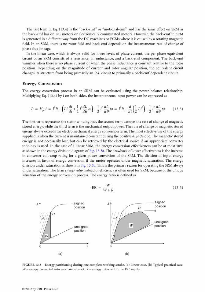
The last term in Eq. (13.4) is the “back-emf” or “motional-emf” and has the same effect on SRM asthe back-emf has on DC motors or electronically commutated motors. However, the back-emf in SRMis generated in a different way from the DC machines or ECMs where it is caused by a rotating magneticfield. In an SRM, there is no rotor field and back-emf depends on the instantaneous rate of change ofphase flux linkage.
In the linear case, which is always valid for lower levels of phase current, the per phase equivalentcircuit of an SRM consists of a resistance, an inductance, and a back-emf component. The back-emfvanishes when there is no phase current or when the phase inductance is constant relative to the rotorposition. Depending on the magnitude of current and rotor angular position, the equivalent circuitchanges its structure from being primarily an R-L circuit to primarily a back-emf dependent circuit.
Energy Conversion
The energy conversion process in an SRM can be evaluated using the power balance relationship.Multiplying Eq. (13.4) by i on both sides, the instantaneous input power can be expressed as
(13.5)
The first term represents the stator winding loss, the second term denotes the rate of change of magneticstored energy, while the third term is the mechanical output power. The rate of change of magnetic storedenergy always exceeds the electromechanical energy conversion term. The most effective use of the energysupplied is when the current is maintained constant during the positive dL/dθ slope. The magnetic storedenergy is not necessarily lost, but can be retrieved by the electrical source if an appropriate convertertopology is used. In the case of a linear SRM, the energy conversion effectiveness can be at most 50%as shown in the energy division diagram of Fig. 13.3a. The drawback of lower effectiveness is the increasein converter volt-amp rating for a given power conversion of the SRM. The division of input energyincreases in favor of energy conversion if the motor operates under magnetic saturation. The energydivision under saturation is shown in Fig. 13.3b. This is the primary reason for operating the SRM alwaysunder saturation. The term energy ratio instead of efficiency is often used for SRM, because of the uniquesituation of the energy conversion process. The energy ratio is defined as
(13.6)
FIGURE 13.3 Energy partitioning during one complete working stroke. (a) Linear case. (b) Typical practical case.W = energy converted into mechanical work. R = energy returned to the DC supply.
P Vphi i2R Lididt----- 1
2-- i2dL
dq------ w+
12-- i2 dL
dq------ w+ + i2R
ddt----- 1
2-- Li2
1
2-- i2 dL
dq------ w+ += = =
ERW
W R+---------------=
unaligned position
i0
W
RC
unaligned position
λ
0
W
R
C
(a) (b)
λ
θ
aligned position
aligned position
© 2002 by CRC Press LLC
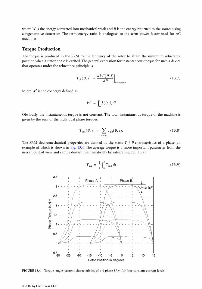
where W is the energy converted into mechanical work and R is the energy returned to the source usinga regenerative converter. The term energy ratio is analogous to the term power factor used for ACmachines.
Torque Production
The torque is produced in the SRM by the tendency of the rotor to attain the minimum reluctanceposition when a stator phase is excited. The general expression for instantaneous torque for such a devicethat operates under the reluctance principle is
(13.7)
where W ′ is the coenergy defined as
Obviously, the instantaneous torque is not constant. The total instantaneous torque of the machine isgiven by the sum of the individual phase torques.
(13.8)
The SRM electromechanical properties are defined by the static T–i–θ characteristics of a phase, anexample of which is shown in Fig. 13.4. The average torque is a more important parameter from theuser’s point of view and can be derived mathematically by integrating Eq. (13.8).
(13.9)
FIGURE 13.4 Torque–angle–current characteristics of a 4-phase SRM for four constant current levels.
Tph(q, i)∂ W′ q, i( )
∂q------------------------
i=constant
=
W′ l q, i( ) id0
i
∫=
Tinst q, i( ) Tph q, i( ).phases∑=
Tavg1T--- Tinst td
0
T
∫=
-30 -25 -20 -15 -10 -5 0 5 10 15-0.5
0
0.5
1
1.5
2
2.5
3
3.5
Rotor Position in degrees
Phase A Phase B
Torque dip
Pha
se T
orqu
e in
N.m
© 2002 by CRC Press LLC
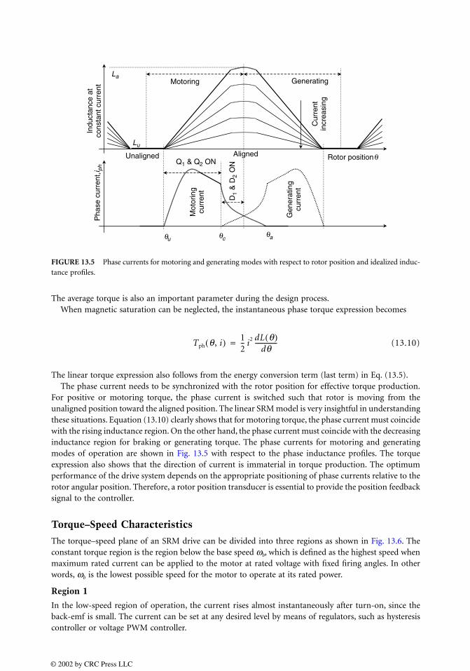
The average torque is also an important parameter during the design process.When magnetic saturation can be neglected, the instantaneous phase torque expression becomes
(13.10)
The linear torque expression also follows from the energy conversion term (last term) in Eq. (13.5).The phase current needs to be synchronized with the rotor position for effective torque production.
For positive or motoring torque, the phase current is switched such that rotor is moving from theunaligned position toward the aligned position. The linear SRM model is very insightful in understandingthese situations. Equation (13.10) clearly shows that for motoring torque, the phase current must coincidewith the rising inductance region. On the other hand, the phase current must coincide with the decreasinginductance region for braking or generating torque. The phase currents for motoring and generatingmodes of operation are shown in Fig. 13.5 with respect to the phase inductance profiles. The torqueexpression also shows that the direction of current is immaterial in torque production. The optimumperformance of the drive system depends on the appropriate positioning of phase currents relative to therotor angular position. Therefore, a rotor position transducer is essential to provide the position feedbacksignal to the controller.
Torque–Speed Characteristics
The torque–speed plane of an SRM drive can be divided into three regions as shown in Fig. 13.6. Theconstant torque region is the region below the base speed ωb, which is defined as the highest speed whenmaximum rated current can be applied to the motor at rated voltage with fixed firing angles. In otherwords, ωb is the lowest possible speed for the motor to operate at its rated power.
Region 1
In the low-speed region of operation, the current rises almost instantaneously after turn-on, since theback-emf is small. The current can be set at any desired level by means of regulators, such as hysteresiscontroller or voltage PWM controller.
FIGURE 13.5 Phase currents for motoring and generating modes with respect to rotor position and idealized induc-tance profiles.
Indu
ctan
ce a
tco
nsta
nt c
urre
nt
u c a
Pha
se c
urre
nt,i p
h
Unaligned
Lu
La Motoring Generating
Mot
orin
gcu
rren
t
Gen
erat
ing
curr
ent
Cur
rent
incr
easi
ng
Rotor position Q1 & Q2 ON
D1
& D
2 O
N
Aligned θ
θθθ
Tph q, i( ) 12-- i2 dL q( )
dq--------------=
© 2002 by CRC Press LLC
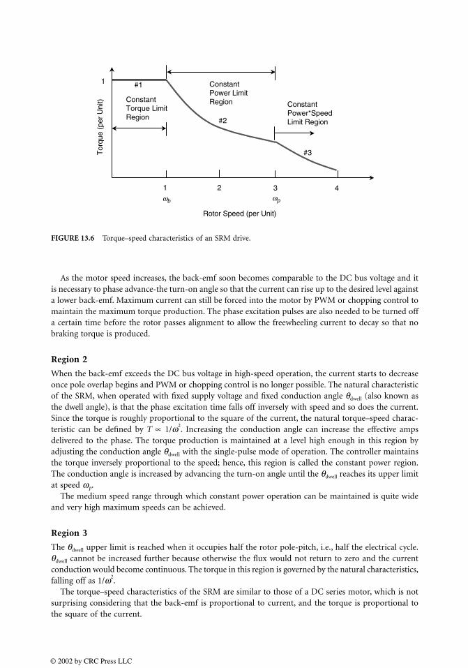
As the motor speed increases, the back-emf soon becomes comparable to the DC bus voltage and itis necessary to phase advance-the turn-on angle so that the current can rise up to the desired level againsta lower back-emf. Maximum current can still be forced into the motor by PWM or chopping control tomaintain the maximum torque production. The phase excitation pulses are also needed to be turned offa certain time before the rotor passes alignment to allow the freewheeling current to decay so that nobraking torque is produced.
Region 2
When the back-emf exceeds the DC bus voltage in high-speed operation, the current starts to decreaseonce pole overlap begins and PWM or chopping control is no longer possible. The natural characteristicof the SRM, when operated with fixed supply voltage and fixed conduction angle θdwell (also known asthe dwell angle), is that the phase excitation time falls off inversely with speed and so does the current.Since the torque is roughly proportional to the square of the current, the natural torque–speed charac-teristic can be defined by T ∝ 1/ω2
. Increasing the conduction angle can increase the effective ampsdelivered to the phase. The torque production is maintained at a level high enough in this region byadjusting the conduction angle θdwell with the single-pulse mode of operation. The controller maintainsthe torque inversely proportional to the speed; hence, this region is called the constant power region.The conduction angle is increased by advancing the turn-on angle until the θdwell reaches its upper limitat speed ωp.
The medium speed range through which constant power operation can be maintained is quite wideand very high maximum speeds can be achieved.
Region 3
The θdwell upper limit is reached when it occupies half the rotor pole-pitch, i.e., half the electrical cycle.θdwell cannot be increased further because otherwise the flux would not return to zero and the currentconduction would become continuous. The torque in this region is governed by the natural characteristics,falling off as 1/ω2
.The torque–speed characteristics of the SRM are similar to those of a DC series motor, which is not
surprising considering that the back-emf is proportional to current, and the torque is proportional tothe square of the current.
FIGURE 13.6 Torque–speed characteristics of an SRM drive.
p b
#1
#2
#3
Rotor Speed (per Unit)
1 2 4 3
Tor
que
(per
Uni
t)
1
Constant Torque Limit Region
Constant Power Limit Region Constant
Power*Speed Limit Region
ω ω
© 2002 by CRC Press LLC

13.4 Design
The fundamental design rules governing the choice of phase numbers, pole numbers, and pole arcs werediscussed in detail by Lawrenson et al. [2] and also by Miller [3]. From a designer’s point of view, theobjectives are to minimize the core losses, to have good starting capability, to minimize the unwantedeffects due to varying flux distributions and saturation, and to eliminate mutual coupling. The choiceof the number of phases and poles is open, but a number of factors need to be evaluated prior to makinga selection.
The fundamental switching frequency is given by
(13.11)
where N is the motor speed in rev/m and Nr is the number of rotor poles. The “step angle” or “stroke”of an SRM is given by
(13.12)
The stoke angle is an important design parameter related to the frequency of control per rotor revolution.Nrep represents the multiplicity of the basic SRM configuration, which can also be stated as the numberof pole pairs per phase. Nph is the number of phases. Nph and Nrep together set the number of stator poles.
The regular choice of the number of rotor poles in an SRM is
(13.13)
where k is an integer such that k mod q ≠ 0 and Ns is the number of stator poles. Some combinations ofparameters allowed by Eq. (13.13) are not feasible, since sufficient space must exist between the poles forthe windings. The most common choice for the selection of stator and rotor pole number for Eq. (13.13) iskm = 2 with the negative sign.
The torque is produced during the partial overlap region between the stator and rotor pole arcs, and,hence, we must have
min(βr , βs) > ε
where βr and βs are the rotor and stator pole arcs, respectively. Practical designs must insure that therotor interpolar gap is greater than the stator pole arc so that the minimum possible unaligned inductancecan be obtained to get the largest possible phase inductance variation between the aligned and unalignedrotor positions. The consideration leads to the second constraint:
The above constraint prevents simultaneous overlap of one stator pole by two rotor poles.The angular rate of change of phase flux can be doubled by doubling Nrep (while other parameters are
held constant with all the coils of each phase connected in series), since this does not affect the maximumand minimum inductances. However, the torque remains unaffected, since the number of turns needsto be halved to keep the back-emf the same when Nrep is doubled. Further consideration of the rate ofchange of flux linkage, available coil area, saliency ratio, split ratio (ratio between rotor radius and motoroutside radius), variation in the magnetic circuit reluctance, saturation behavior, and the iron loss dueto the increase of the repetition modifies this simplistic conclusion. The advantages of increasing Nrep
fN60-----Nr Hz=
Step Angle e 2pNph Nrep Nr⋅ ⋅---------------------------------=
Nr Ns km±=
2pNr
------ br– bs>
© 2002 by CRC Press LLC

are greater fault-tolerance and shorter flux-paths leading to lower core losses compared to the single-repetition machines. The contribution to the mean torque can also be increased in multiple repetitionmachines if the pole width is made more than 50% of that for a single-repetition machine. For Nrep = 2,the stator pole width needs to be approximately 70% of that of the single-repetition machine with theoptimization criterion of maximizing the co-energy both under high and low current conditions [5].This gives about 40% more thermally limited torque and horizontal force for the same copper loss andtotal volume.
The highest possible saliency ratio (the ratio between the maximum and minimum unsaturatedinductance levels) is desired to achieve the highest possible torque per ampere, but as the rotor and statorpole arcs are decreased the torque ripple tends to increase. The torque ripple adversely affects the dynamicperformance of an SRM drive. For many applications, it is desirable to minimize the torque ripple, whichcan be partially achieved through appropriate design. The torque dip observed in the T−i−θ characteristicsof an SRM (see Fig. 13.4) is an indirect measure of the torque ripple expected in the drive system. Thetorque dip is the difference between the peak torque of a phase and the torque at an angle where twooverlapping phases produce equal torque at equal levels of current. The smaller the torque dip, the lesswill be the torque ripple. The T−i−θ characteristics of the SRM depend on the stator-rotor pole overlapangle, pole geometry, material properties, number of poles and number of phases. A design trade-offneeds to be considered to achieve the desired goals. The T−i−θ characteristics must be studied throughfinite element analysis during the design stage to evaluate both the peak torque and torque dip values.
Increasing the number of strokes per revolution can alleviate the problem of torque dips and hencethe torque ripple. One way of achieving this is with a larger Nr, but the method has an associated penaltyin the saliency ratio [2, 3]. The decrease in saliency ratio with increasing Nr will increase the controllervolt-amps and decrease the torque output. The higher switching frequency will also increase the corelosses. Increasing the phase numbers with a much smaller penalty in the saliency ratio is a better approachfor reducing the torque dips. The average torque of the machine will also increase because of the smallertorque dips. The higher number of phases will increase the overlap between phase torques in the regionsof commutation. The torque ripple can then be minimized through a controller algorithm that profilesthe overlapping phase currents of adjacent phases during commutation. The SRMs with three or lowernumber of phases suffer more from the problem of torque dips near the commutation region. The four-or five-phase machines can deliver uniform torque without exceedingly boosting the current in rotorpositions of low phase-torque per ampere. The cost and complexity of the drive increases with higher phasenumbers, since additional switches are required for the power converter. In general, two- or three-phasemachines are used in high-speed applications, while four-phase machines are chosen where torque-rippleis a concern.
The inductance overlap ratio KL, which is the ratio of unsaturated inductance overlap of two adjacentphases to the angle over which the inductance is changing [1, 4], can be utilized during the design phaseto analyze the torque characteristics. The ratio gives a direct measure of the torque overlap of adjacentphases. The higher the KL, the lower will be the torque dip and the higher will be the mean torque aswell. Mathematically, the inductance ratio is defined as
(13.14)
The torque overlap can be increased by widening the stator and rotor poles. Figures 13.7 and 13.8 plot KL
vs. βs (assuming βs ≤ βr) and KL vs. Nph (assuming βs for Nrep = 2 to be 70% of that of βs for Nrep = 1).Figure 13.7 shows that high values of KL are achievable at relatively low values of βs for a machine withmore phases and/or repetitions. The same machines have better starting capabilities. Also, the rate of changeof KL with respect to βs is much higher near the minimum possible values for βs. Additionally, a relativelyhigher stator pole width will reduce the available window area for winding and increase the copper losses.Therefore, the βs should not be increased significantly from its minimum possible value. Figure 13.8 showsthat the improvement on the problem of torque dip is noticeable in the lower range of Nph.
KL 1e
min bs, br( )----------------------------–=
© 2002 by CRC Press LLC
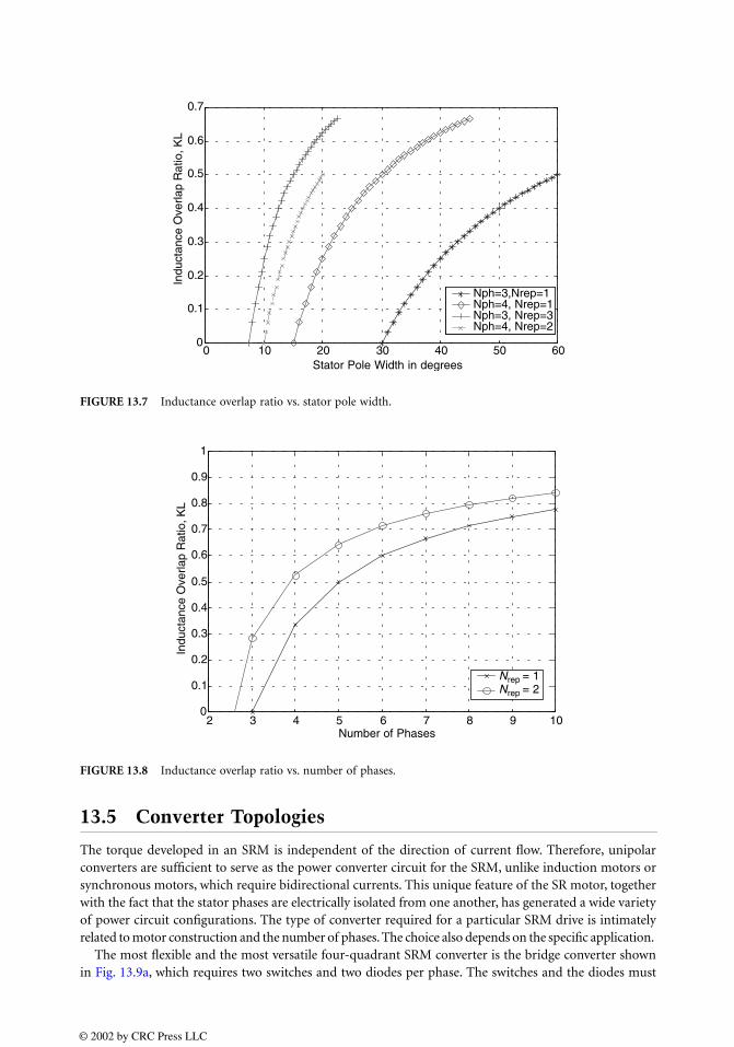
13.5 Converter Topologies
The torque developed in an SRM is independent of the direction of current flow. Therefore, unipolarconverters are sufficient to serve as the power converter circuit for the SRM, unlike induction motors orsynchronous motors, which require bidirectional currents. This unique feature of the SR motor, togetherwith the fact that the stator phases are electrically isolated from one another, has generated a wide varietyof power circuit configurations. The type of converter required for a particular SRM drive is intimatelyrelated to motor construction and the number of phases. The choice also depends on the specific application.
The most flexible and the most versatile four-quadrant SRM converter is the bridge converter shownin Fig. 13.9a, which requires two switches and two diodes per phase. The switches and the diodes must
FIGURE 13.7 Inductance overlap ratio vs. stator pole width.
FIGURE 13.8 Inductance overlap ratio vs. number of phases.
0 10 20 30 40 50 600
0.1
0.2
0.3
0.4
0.5
0.6
0.7
Stator Pole Width in degrees
Nph=3,Nrep=1Nph=4, Nrep=1Nph=3, Nrep=3Nph=4, Nrep=2
Indu
ctan
ce O
verla
p R
atio
, KL
2 3 4 5 6 7 8 9 100
0.1
0.2
0.3
0.4
0.5
0.6
0.7
0.8
0.9
1
Number of Phases
Nrep = 1Nrep = 2
Indu
ctan
ce O
verla
p R
atio
, KL
© 2002 by CRC Press LLC
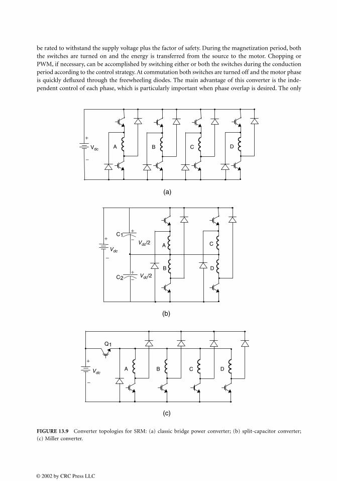
be rated to withstand the supply voltage plus the factor of safety. During the magnetization period, boththe switches are turned on and the energy is transferred from the source to the motor. Chopping orPWM, if necessary, can be accomplished by switching either or both the switches during the conductionperiod according to the control strategy. At commutation both switches are turned off and the motor phaseis quickly defluxed through the freewheeling diodes. The main advantage of this converter is the inde-pendent control of each phase, which is particularly important when phase overlap is desired. The only
FIGURE 13.9 Converter topologies for SRM: (a) classic bridge power converter; (b) split-capacitor converter;(c) Miller converter.
(a)
(b)
(c)
−
+
A B C D
− +
−
+ C1
C2
B D
A Vdc
Vdc/2
Vdc/2
Vdc
Vdc
−
+ C
Q1
−
+ A B C D
© 2002 by CRC Press LLC
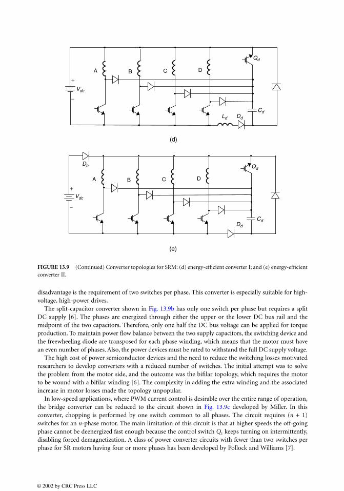
disadvantage is the requirement of two switches per phase. This converter is especially suitable for high-voltage, high-power drives.
The split-capacitor converter shown in Fig. 13.9b has only one switch per phase but requires a splitDC supply [6]. The phases are energized through either the upper or the lower DC bus rail and themidpoint of the two capacitors. Therefore, only one half the DC bus voltage can be applied for torqueproduction. To maintain power flow balance between the two supply capacitors, the switching device andthe freewheeling diode are transposed for each phase winding, which means that the motor must havean even number of phases. Also, the power devices must be rated to withstand the full DC supply voltage.
The high cost of power semiconductor devices and the need to reduce the switching losses motivatedresearchers to develop converters with a reduced number of switches. The initial attempt was to solvethe problem from the motor side, and the outcome was the bifilar topology, which requires the motorto be wound with a bifilar winding [6]. The complexity in adding the extra winding and the associatedincrease in motor losses made the topology unpopular.
In low-speed applications, where PWM current control is desirable over the entire range of operation,the bridge converter can be reduced to the circuit shown in Fig. 13.9c developed by Miller. In thisconverter, chopping is performed by one switch common to all phases. The circuit requires (n + 1)switches for an n-phase motor. The main limitation of this circuit is that at higher speeds the off-goingphase cannot be deenergized fast enough because the control switch Q1 keeps turning on intermittently,disabling forced demagnetization. A class of power converter circuits with fewer than two switches perphase for SR motors having four or more phases has been developed by Pollock and Williams [7].
FIGURE 13.9 (Continued) Converter topologies for SRM: (d) energy-efficient converter I; and (e) energy-efficientconverter II.
(d)
(e)
Vdc
QdDb
CdDd
DdLd
Qd
Cd
Vdc
−
+
A B C D
−
+
A B C D
© 2002 by CRC Press LLC

The energy-efficient C-dump converters I and II are two regenerative converter topologies with areduced number of switches [8]. The converters are shown in Figs. 13.9d and e. The topologies werederived from the C-dump converter proposed earlier by Ehsani et al. [9]. The energy efficient convertertopologies eliminate all the disadvantages of the C-dump converter without sacrificing its attractivefeatures, and also provide some additional advantages. The attractive features of the converters are: lowernumber of power devices, full regenerative capability, freewheeling in chopping or PWM mode, simplecontrol strategy, and faster demagnetization during commutation. Energy-efficient C-dump converter Ihas only one-switch forward voltage drop, whereas energy-efficient C-dump converter II has one-switchplus one diode forward voltage drop in the phase magnetization paths. The dump component energyrequirements are much lower in these converters compared with those of the C-dump converter.
Converters with a reduced number of switches are typically less fault tolerant compared with the bridgeconverter. The ability to survive component or motor phase failure should be a prime consideration forhigh-reliability applications. On the other hand, in low-voltage applications, the voltage drop in twoswitches can be a significant percentage of the total bus voltage, which may not be affordable. Otherfactors to be considered in selecting a drive circuit include cost, complexity in control, number of passivecomponents, number of floating drivers required, etc. The drive converter must be chosen to serve theparticular needs of an application.
13.6 Control Strategies
Appropriate positioning of the phase excitation pulses relative to the rotor position is the key to obtainingeffective performance from an SRM drive system. The turn-on time, the total conduction period, andthe magnitude of the phase current determine torque, efficiency, and other performance parameters. Thetype of control to be employed depends on the operating speed of the SRM.
Control Parameters
The control parameters for an SRM drive are the turn-on angle (θon), turn-off angle (θoff), and the phasecurrent. The conduction angle is defined as θdwell = θoff − θon. The complexity of determination of the controlparameters depends on the chosen control method for a particular application. The current commandcan be generated for one or more phases depending on the controller. In voltage-controlled drives, thecurrent is indirectly regulated by controlling the phase voltage.
At low speeds, the current rises almost instantaneously after turn-on because of the negligible back-emf, and the current must be limited by either controlling the average voltage or regulating the currentlevel. The type of control used has a marked effect on the performance of the drive. As the speed increases,the back-emf increases as explained before and opposes the applied bus voltage. Phase advancing isnecessary to establish the phase current at the onset of rotor and stator pole overlap region. Voltage PWMor chopping control is used to force maximum current into the motor to maintain the desired torquelevel. Also, the phase excitation is turned off early enough so that the phase current decays completelyto zero before the negative torque-producing region is reached.
At higher-speeds, the SRM enters the single-pulse mode of operation, and control is achieved byadvancing the turn-on angle and adjusting the conduction angle. At very high speeds, the back-emf willexceed the applied bus voltage once the current magnitude is high and the rotor position is appropriate,which causes the current to decrease after reaching a peak even though a positive bus voltage is appliedduring the positive dL/dθ. The control algorithm outputs θdwell and θon according to speed. At the endof θdwell the phase switches are turned off so that negative voltage is applied across the phase to commutatethe phase as quickly as possible. The back-emf reverses polarity beyond the aligned position and maycause the current to increase in this region if the current does not decay to insignificant levels. Therefore,the phase commutation must precede the aligned position by several degrees so that the current decaysbefore the negative dL/dθ region is reached.
© 2002 by CRC Press LLC
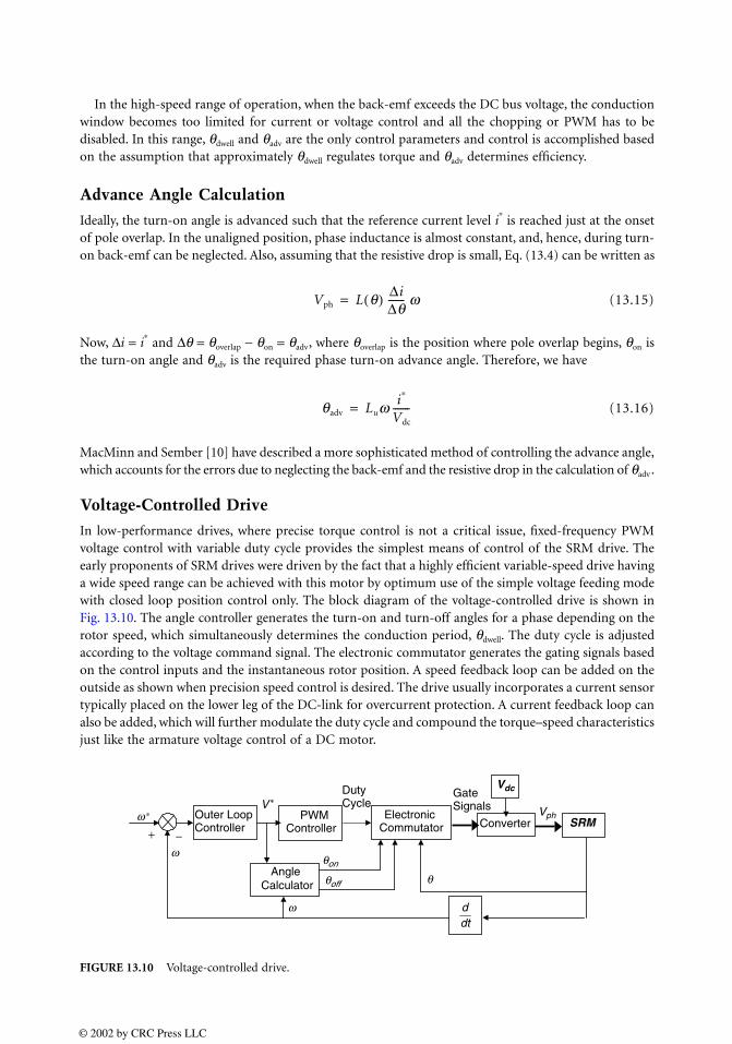
In the high-speed range of operation, when the back-emf exceeds the DC bus voltage, the conductionwindow becomes too limited for current or voltage control and all the chopping or PWM has to bedisabled. In this range, θdwell and θadv are the only control parameters and control is accomplished basedon the assumption that approximately θdwell regulates torque and θadv determines efficiency.
Advance Angle Calculation
Ideally, the turn-on angle is advanced such that the reference current level i∗ is reached just at the onset
of pole overlap. In the unaligned position, phase inductance is almost constant, and, hence, during turn-on back-emf can be neglected. Also, assuming that the resistive drop is small, Eq. (13.4) can be written as
(13.15)
Now, ∆i = i∗ and ∆θ = θoverlap − θon = θadv, where θoverlap is the position where pole overlap begins, θon is
the turn-on angle and θadv is the required phase turn-on advance angle. Therefore, we have
(13.16)
MacMinn and Sember [10] have described a more sophisticated method of controlling the advance angle,which accounts for the errors due to neglecting the back-emf and the resistive drop in the calculation of θadv .
Voltage-Controlled Drive
In low-performance drives, where precise torque control is not a critical issue, fixed-frequency PWMvoltage control with variable duty cycle provides the simplest means of control of the SRM drive. Theearly proponents of SRM drives were driven by the fact that a highly efficient variable-speed drive havinga wide speed range can be achieved with this motor by optimum use of the simple voltage feeding modewith closed loop position control only. The block diagram of the voltage-controlled drive is shown inFig. 13.10. The angle controller generates the turn-on and turn-off angles for a phase depending on therotor speed, which simultaneously determines the conduction period, θdwell. The duty cycle is adjustedaccording to the voltage command signal. The electronic commutator generates the gating signals basedon the control inputs and the instantaneous rotor position. A speed feedback loop can be added on theoutside as shown when precision speed control is desired. The drive usually incorporates a current sensortypically placed on the lower leg of the DC-link for overcurrent protection. A current feedback loop canalso be added, which will further modulate the duty cycle and compound the torque–speed characteristicsjust like the armature voltage control of a DC motor.
FIGURE 13.10 Voltage-controlled drive.
Vph L q( ) ∆i∆q------- w=
qadv Luw i∗
Vdc
-------=
Vph
θoff
DutyCycle
V*
θ
θon
GateSignals
− +
Outer Loop Controller
PWMController SRM Electronic
Commutator Converter
Vdc
Angle Calculator
dtd
ω∗
ω
ω
© 2002 by CRC Press LLC
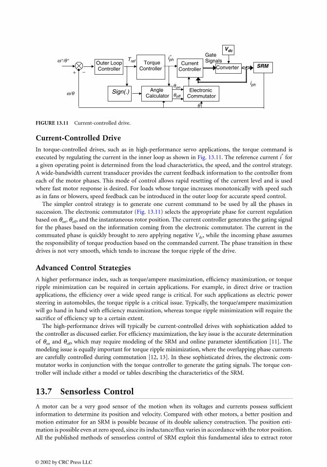
Current-Controlled Drive
In torque-controlled drives, such as in high-performance servo applications, the torque command isexecuted by regulating the current in the inner loop as shown in Fig. 13.11. The reference current i
∗ for
a given operating point is determined from the load characteristics, the speed, and the control strategy.A wide-bandwidth current transducer provides the current feedback information to the controller fromeach of the motor phases. This mode of control allows rapid resetting of the current level and is usedwhere fast motor response is desired. For loads whose torque increases monotonically with speed suchas in fans or blowers, speed feedback can be introduced in the outer loop for accurate speed control.
The simpler control strategy is to generate one current command to be used by all the phases insuccession. The electronic commutator (Fig. 13.11) selects the appropriate phase for current regulationbased on θon, θoff, and the instantaneous rotor position. The current controller generates the gating signalfor the phases based on the information coming from the electronic commutator. The current in thecommuated phase is quickly brought to zero applying negative Vdc, while the incoming phase assumesthe responsibility of torque production based on the commanded current. The phase transition in thesedrives is not very smooth, which tends to increase the torque ripple of the drive.
Advanced Control Strategies
A higher performance index, such as torque/ampere maximization, efficiency maximization, or torqueripple minimization can be required in certain applications. For example, in direct drive or tractionapplications, the efficiency over a wide speed range is critical. For such applications as electric powersteering in automobiles, the torque ripple is a critical issue. Typically, the torque/ampere maximizationwill go hand in hand with efficiency maximization, whereas torque ripple minimization will require thesacrifice of efficiency up to a certain extent.
The high-performance drives will typically be current-controlled drives with sophistication added tothe controller as discussed earlier. For efficiency maximization, the key issue is the accurate determinationof θon and θoff, which may require modeling of the SRM and online parameter identification [11]. Themodeling issue is equally important for torque ripple minimization, where the overlapping phase currentsare carefully controlled during commutation [12, 13]. In these sophisticated drives, the electronic com-mutator works in conjunction with the torque controller to generate the gating signals. The torque con-troller will include either a model or tables describing the characteristics of the SRM.
13.7 Sensorless Control
A motor can be a very good sensor of the motion when its voltages and currents possess sufficientinformation to determine its position and velocity. Compared with other motors, a better position andmotion estimator for an SRM is possible because of its double saliency construction. The position esti-mation is possible even at zero speed, since its inductance/flux varies in accordance with the rotor position.All the published methods of sensorless control of SRM exploit this fundamental idea to extract rotor
FIGURE 13.11 Current-controlled drive.
Sign(.)off
GateSignals Tref
− +
Outer Loop Controller
ω∗/θ∗
ω/θ
CurrentController
TorqueController SRM
∗iph
Electronic Commutator
Converter
iph
Vdc
Angle Calculator
θon
θ
θ
© 2002 by CRC Press LLC

position information by measuring either inductance or flux. A wide variety of methods have beenproposed to eliminate the rotor position transducer over the past decade, which evolved with their ownmerits and demerits.
The various methods of indirect-position sensing reported so far in the literature fall under one ofthe following divisions:
• Phase current monitoring–based estimation [14].
• Phase flux measurement–based position estimation [15].
• Observer-based position estimation (Luenberger observer, sliding-mode observer, Kalman filter,etc.) [16, 17].
• Position estimation by pulse injection into an idle phase [18–21].
• Mutual voltage sensing–based system [22].
• Artificial intelligence–based position estimation (artificial neural network, fuzzy logic, etc.) [23, 24].
The methods of indirect position sensing can be broadly classified into two categories: (1) Nonintrusivemethods, where position information is obtained from terminal measurements of voltages and currentsand associated computations, and (2) intrusive (or active probing) methods, where low-level, high-frequency signals are injected into an idle phase to determine the position. Further classification of thebroad categories is shown in Fig. 13.12.
Nonintrusive methods: The nonintrusive methods rely on the machine characteristics for estimatingthe rotor position. The terminal measurements of phase voltage or mutual voltage and current are usedas inputs for an estimator to obtain the rotor position. The features of the nonintrusive methods are:
• Based on machine characteristics.
• Flux of jth
phase is obtained from the integration of flux-inducing voltage,
(13.17)
• The position information is obtained from flux and phase current information using the machinecharacteristics:
FIGURE 13.12 Classification of indirect rotor-position sensing methods for SRM.
lj vj ijrj–( )dt=
l i, q( ) q⇒
Flux Sensing
FM AM/PM
Active Probing Methods
Indirect Position Sensing
Non-Intrusive Methods
Open-Loop
Waveform Detection
Flux/Current Method
Mutual Voltage Method
Observer Based
Passive Waveform Detection
Modulation Based
AM Artificial Intelligence Based
© 2002 by CRC Press LLC
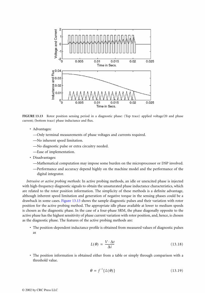
• Advantages:
—Only terminal measurements of phase voltages and currents required.
—No inherent speed limitation.
—No diagnostic pulse or extra circuitry needed.
—Ease of implementation.
• Disadvantages:
—Mathematical computation may impose some burden on the microprocessor or DSP involved.
—Performance and accuracy depend highly on the machine model and the performance of thedigital integrator.
Intrusive or active probing methods: In active probing methods, an idle or unexcited phase is injectedwith high-frequency diagnostic signals to obtain the unsaturated phase inductance characteristics, whichare related to the rotor position information. The simplicity of these methods is a definite advantage,although inherent speed limitation and generation of negative torque in the sensing phases could be adrawback in some cases. Figure 13.13 shows the sample diagnostic pulses and their variation with rotorposition for the active probing method. The appropriate idle phase available at lower to medium speedsis chosen as the diagnostic phase. In the case of a four-phase SRM, the phase diagonally opposite to theactive phase has the highest sensitivity of phase current variation with rotor position, and, hence, is chosenas the diagnostic phase. The features of the active probing methods are:
• The position-dependent inductance profile is obtained from measured values of diagnostic pulsesas
(13.18)
• The position information is obtained either from a table or simply through comparison with athreshold value.
(13.19)
FIGURE 13.13 Rotor position sensing period in a diagnostic phase: (Top trace) applied voltage/20 and phasecurrent; (bottom trace) phase inductance and flux.
L q( ) V ∆t⋅∆i
--------------=
q f 1– L q( ) =
© 2002 by CRC Press LLC

• Advantages:
—Well suited for low-speed application.
—Diagnostic pulse can be injected using the same power converter.
—Self-starting can be implemented using the same probing pulses.
• Disadvantages:
—Inherent speed limitations due to the pulse injection.
—Unnecessary negative torque generation.
—Needs extra circuitry in some cases, which adds cost and complexity to the overall drive system.
Continuous rotor position information can be obtained from indirect position sensing schemes by amapping of inductance, flux, or current waveforms to rotor position. Alternatively, the task can besimplified in less sophisticated algorithms by threshold comparison of the indirectly measured positioninformation to effectuate commutation. Phase advancing and retardation is possible by changing thethreshold level appropriately.
13.8 Applications
The simple motor structure and inexpensive power electronic requirement have made the SRM anattractive alternative to both AC and DC machines in adjustable-speed drives. An example of SRMapplication is in heating, ventilation, and air conditioning (HVAC) systems. Here, the high-speedcapability, low cost, ruggedness, and fault tolerance features of the SRM drive can produce low-costadjustable-speed HVAC products for the consumer market. The appliance industry can also benefit fromthe low-cost and ruggedness of SRM drives. The Maytag Neptune washer uses a three-phase SRM drivefor its high-end products. Ametek-Lamb Electric is also commercially manufacturing a heavy-duty vacuum/blower using SRM drives.
SRM drives have great potential for use within the various aspects of conventional automobiles. Inthis application, the SRM drive can be very simple, inexpensive, compatible with the low battery voltagein the car, very rugged, and fault-tolerant. The absence of temperature sensitivity in the harsh environ-ment under the hood is a definite plus for SRM drives in comparison with permanent magnet motordrives. Example applications of SRMs within an automobile are for the electric power steering andantilock braking systems. The SRM drive is also a strong candidate for the main propulsion drive of anelectric or hybrid vehicle. The wide constant power range of SRM drives is especially suitable for suchapplications. Electric Motorbike, Inc. has developed the Lectra motorcycle based on an SRM drive.
The SRM is also suitable for many industrial and manufacturing applications. For example, high-speed adjustable-speed pumping of fluids for a variety of petrochemical, food processing, and otherapplications can be done with large horsepower SRM drives. The fact that the SRM can operate underpartial converter and motor failure means that these pumps can be placed in critical links in the processcontrol loop. Other high-technology applications for which the SRM drives are being considered includerobotic prime movers, aerospace starter/generators, fuel pumps, and servo systems.
Although sophisticated controllers are being designed for SRM drives, it must be realized that the simplePWM voltage control provides a highly efficient variable-speed drive that can be operated over a widespeed range. This mode of operation is usually adequate for a number of motion control applications.
References
1. J. V. Byrne et al., A high performance variable reluctance motor drive: a new brushless servo, inMotorcon Proc., 1985, 147–160.
2. P. J. Lawrenson, J. M. Stephenson, P. T. Blenkinsop, J. Corda, and N. N. Fulton, Variable-speedswitched reluctance motors, IEE Proc. B, 127(4), 253–265, 1980.
© 2002 by CRC Press LLC

3. T. J. E. Miller, Switched Reluctance Motors and Their Control, Magna Physics Publishing, Hillsboro,OH; and Oxford Science Publications, Oxford, U.K., 1993.
4. M. N. Anwar, I. Husain, and A. V. Radun, A comprehensive design methodology for switched reluc-tance machines, in IEEE-IAS Annual Conf., Rome, Italy, Oct. 2000.
5. H. C. Lovatt and J. M. Stephenson, Influence of the number of poles per phase in switched reluctancemotors, IEE Proc. B, 139(4), 307–314, 1992.
6. R. M. Davis, W. F. Ray, and R. J. Blake, Inverter drive for switched reluctance motor: circuits andcomponent ratings, in IEE Proc., 128B(2), 126–136, 1981.
7. C. Pollock and B. W. Williams, Power converter circuits for switched reluctance motors with theminimum number of switches, IEE Proc., 137B(6), 373–384, 1990.
8. S. Mir, I. Husain, and M. Elbuluk, Energy-efficient C-dump converters for switched reluctance motors,IEEE Trans. Power Electronics, 12(5), 912–921, 1997.
9. M. Ehsani, J. T. Bass, T. J. E. Miller, and R. L. Steigerwald, Development of a unipolar converter forvariable reluctance motor drives, IEEE Trans. Ind. Appl., IA-23(3), 545–553, 1987.
10. S. R. MacMinn and J. W. Sember, Control of a switched-reluctance aircraft engine starter-generatorover a very wide speed range, in IECEC Conf. Rec., Aug. 1989, 631–638.
11. S. Mir, I. Husain, and M. Elbuluk, Switched reluctance motor modeling with on-line parameteradaptation, IEEE Trans. Ind. Appl., 34(4), 776–783, 1998.
12. K. Russa, I. Husain, and M. Elbuluk, Torque ripple minimization in switched reluctance machinesover a wide speed range, IEEE Trans. Ind. Appl., 34(5), 1105–1112, 1998.
13. S. Mir, M. Elbuluk, and I. Husain, Torque ripple minimization in switched reluctance motors usingan adaptive fuzzy control, IEEE Trans. Ind. Appl., 35(2), 461–468, 1999.
14. P. P. Acarnley, R. J. Hill, and C. W. Hooper, Detection of rotor position in stepping and switchedreluctance motors by monitoring of current waveforms, IEEE Trans. Ind. Electron., IE-32(3), 215–222,1985.
15. J. P. Lyons, S. R. MacMinn, and M. A. Preston, Flux/Current methods for SRM rotor positionestimation, in IEEE-IAS Annu. Meet., Dearborn, MI, 1991, 482–487.
16. A. Lumsdaine and J. H. Lang, State observers for variable-reluctance motors, IEEE Trans. Ind.Electron., IE-37(2), 133–142, 1990.
17. I. Husain, S. Sodhi, and M. Ehsani, Sliding mode observer based control for switched reluctancemotors, in IEEE-IAS Conf. Rec. 94, Denver, CO, 1994, 635–643.
18. W. D. Harris and J. H. Lang, A simple motion estimator for variable-reluctance motors, IEEE Trans.Ind. Appl., 26(2), 237–243, 1990.
19. S. R. MacMinn, W. J. Rzesos, P. M. Szczesny, and T. M. Jahns, Application of sensor integrationtechniques to switched reluctance motor drives, IEEE Trans. Ind. Appl., 28(6), 1339–1344, 1992.
20. M. Ehsani, I. Husain, and A. Kulkarni, Elimination of discrete position sensor and current sensorin switched reluctance motor drives, IEEE Trans. Ind. Appl., 28(1), 128–135, 1992.
21. M. Ehsani, I. Husain, S. Mahajan, and K. R. Ramani, New modulation techniques for rotor positionsensing in switched reluctance motors, IEEE Trans. Ind. Appl., 30(1), 85–91, 1994.
22. I. Husain and M. Ehsani, Rotor position sensing in switched reluctance motor drives by measuringmutually induced voltages, IEEE Trans. Ind. Appl., 30(3), 665–672, 1994.
23. E. Mese and D. A. Torrey, Sensorless position estimation for variable-reluctance machines usingartificial neural network, IEEE-IAS Annu. Meeting Proc., 1, 540–547, 1997.
24. A. D. Cheok and N. Ertugal, Use off fuzzy logic for modeling, estimation, and prediction in switchedreluctance motor drives, IEEE Trans. Ind. Electron., 46(6), 1207–1224, 1999.
© 2002 by CRC Press LLC

14Step Motor Drives
14.1 Introduction 14.2 Types and Operation of Step Motors
Variable Reluctance Step Motor • Drive Circuits for Variable Reluctance Step Motors • Permanent Magnet (Can-Stack) Step Motor • Hybrid Step Motor • Drive Circuitry for Permanent Magnet and Hybrid Step Motors
14.3 Step Motor ModelsVariable Reluctance Step Motor Model • Bifilar-Wound Hybrid Step Motor Model • Drive Circuit Modeling
14.4 Control of Step MotorsExcitation of Step Motors • Open-Loop Control
14.1 Introduction
Step motors are used in many low-lost positioning applications due to their inherent ability to stop atdiscrete positions and follow position vs. time profiles while being controlled open loop. A step motoris a synchronous machine, but historically has been used almost exclusively in positioning and positiontracking applications. Recently, however, some types of step motors have been applied in variable speeddrives applications.
Step motors can be driven without feedback to stop at discrete angular positions, known as detent positions.The number of detent positions can be as low as 12 steps or detent positions per revolution to 400 or 500or more steps per revolution. The location accuracy of the detent positions varies typically within 5% of thestep size. The repeatability of the motor is also high, in that the rotor can start on one position, move awayto other positions, and then return to within typically 3% of step size of the original position.
The motors with relatively few steps are typically used in higher-speed applications, where the motorswith many steps per revolution are often used in high-torque, low-speed, direct drive applications orapplications where many repeatable discrete positions are required. Step motors have been successfullyapplied in many applications such as computer peripherals (e.g., disk drives, pen plotters, and printers),office machines (e.g., copiers, scanners), automotive (e.g., seat positioning, speed control), aerospace(e.g., flap control, starter-generators), and industrial (e.g., robots, scanners, machine tools), to name a few.
Many step motor drives are driven with digital pulses, thus it is easy to interface and control stepmotors from computers or microcontrollers without digital to analog circuitry. For control purposes,the step motor and drive can be thought of as a digital to angular position converter.
It is perhaps easier to understand how a step motor works than any other rotating machine. However,the mathematical models of step motors are nonlinear, since the inductance and torque vary sinusoidallywith position. The non-linear nature of the models requires that the engineer carefully design thecontrollers for the motors. In the following section the three types of step motors are discussed alongwith the operation and drive circuits of each. The mathematical models of each type are discussed in thesecond section. In the third section, the control of step motors is presented.
Ronald H. BrownMarquette University
© 2002 by CRC Press LLC

14.2 Types and Operation of Step Motors
The three common types of step motors are the variable reluctance, the permanent magnet, and thehybrid step motors. The variable reluctance and the hybrid step motors are double salient structures, i.e.,teeth on both the stator and the rotor, with multiple windings or phases on the stator and no windingson the rotor (thus brushless machines). The variable reluctance step motors can have three, four, or evenfive phases, while the permanent magnet and the hybrid step motors usually have two phases.
Principle of Operation: A first understanding of the principle of operation can be easily seen from thevariable reluctance step motor, but is common for all types. When a single winding or phase is energized,the motor generates a torque in the direction to align the rotor teeth with the teeth of the energizedphase. The torque generated by current in a single phase, for example, phase A, is
(14.1)
where Te is the generated torque, kT is the torque constant, iA is the current in phase A, Nr is number ofelectrical cycles per mechanical revolution, and θ is the mechanical rotor position. The cross-sectionalview of a variable reluctance step motor is illustrated in Fig. 14.1, showing only the phase A winding.The rotor is shown in the aligned position, which is the detent position. The generated torque by thecurrent in phase A vs. rotor position for this motor is shown in Fig. 14.2. If a load on the rotor were todisplace the rotor in the position θ or clockwise direction, the generated torque would act in the directionto realign the rotor. From Fig. 14.2, we see that a displacement in the positive θ direction generatesnegative torque, which will push the rotor in the negative direction, thus trying to restore the detentposition. If a load on the rotor were to displace the rotor in the negative θ or counterclockwise direction,the generated torque would also act in the direction to realign the rotor. From Fig. 14.2, we see that adisplacement in the negative θ direction generates positive torque, which in turn is in the direction torestore the rotor to the detent position.
Now, suppose the current in phase A is deenergized and phase B is energized. It is apparent fromFig. 14.1 that the rotor will rotate 15° in the positive direction so that rotor teeth will align with thephase B stator teeth. Next, suppose that phase B is deenergized and phase C is energized. The rotor willrotate 15° additionally in the positive direction, aligning phase C stator teeth with rotor teeth. One morephase switching, deenergizing phase C and energizing phase A causes the rotor to rotate yet an additional
FIGURE 14.1 Cross-sectional view.
Te kTiA Nrq( )sin–=
A
A
A
A
B
B
B
B
C
C
C
C
C
S
S
N N
© 2002 by CRC Press LLC
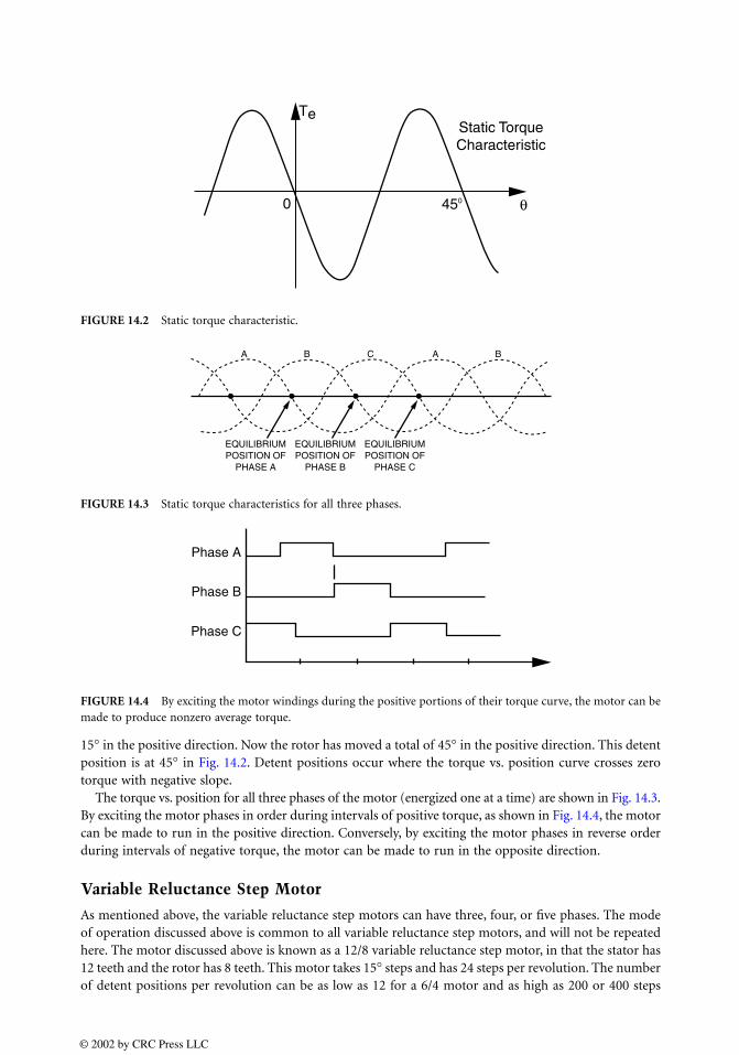
15° in the positive direction. Now the rotor has moved a total of 45° in the positive direction. This detentposition is at 45° in Fig. 14.2. Detent positions occur where the torque vs. position curve crosses zerotorque with negative slope.
The torque vs. position for all three phases of the motor (energized one at a time) are shown in Fig. 14.3.By exciting the motor phases in order during intervals of positive torque, as shown in Fig. 14.4, the motorcan be made to run in the positive direction. Conversely, by exciting the motor phases in reverse orderduring intervals of negative torque, the motor can be made to run in the opposite direction.
Variable Reluctance Step Motor
As mentioned above, the variable reluctance step motors can have three, four, or five phases. The modeof operation discussed above is common to all variable reluctance step motors, and will not be repeatedhere. The motor discussed above is known as a 12/8 variable reluctance step motor, in that the stator has12 teeth and the rotor has 8 teeth. This motor takes 15° steps and has 24 steps per revolution. The numberof detent positions per revolution can be as low as 12 for a 6/4 motor and as high as 200 or 400 steps
FIGURE 14.2 Static torque characteristic.
FIGURE 14.3 Static torque characteristics for all three phases.
FIGURE 14.4 By exciting the motor windings during the positive portions of their torque curve, the motor can bemade to produce nonzero average torque.
0
TeStatic TorqueCharacteristic
450 θ
EQUILIBRIUMPOSITION OF
PHASE A
EQUILIBRIUMPOSITION OF
PHASE B
EQUILIBRIUMPOSITION OF
PHASE C
A B C A B
Phase A
Phase B
Phase C
© 2002 by CRC Press LLC
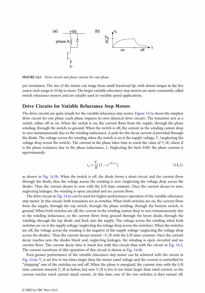
per revolution. The size of the motor can range from small fractional hp, with detent torque in the fewounce-inch range to 10 hp to more. The larger variable reluctance step motors are more commonly calledswitch reluctance motors and are usually used in variable speed applications.
Drive Circuits for Variable Reluctance Step Motors
The drive circuits are quite simple for the variable reluctance step motor. Figure 14.5a shows the simplestdrive circuit for one phase (each phase requires its own identical drive circuit). The transistor acts as aswitch, either off or on. When the switch is on, the current flows from the supply, through the phasewinding, through the switch, to ground. When the switch is off, the current in the winding cannot dropto zero instantaneously due to the winding inductance. A path for the decay current is provided throughthe diode. The voltage across the winding when the switch is on is the supply voltage, Vs (neglecting thevoltage drop across the switch). The current in the phase takes time to reach the value of Vs/R, where Ris the phase resistance due to the phase inductance, L. Neglecting the back EMF, the phase current isapproximately:
(14.2)
as shown in Fig. 14.5b. When the switch is off, the diode forms a short-circuit and the current flowsthrough the diode, thus the voltage across the winding is zero (neglecting the voltage drop across thediode). Thus the current decays to zero with the L/R time constant. Once the current decays to zero,neglecting leakages, the winding is open circuited and no current flows.
The drive circuit in Fig. 14.6a can be used for higher-performance operation of the variable reluctancestep motor. In this circuit, both transistors act as switches. When both switches are on, the current flowsfrom the supply, through the top switch, through the phase winding, through the bottom switch, toground. When both switches are off, the current in the winding cannot drop to zero instantaneously dueto the winding inductance, so the current flows from ground through the lower diode, through thewinding, through the top diode, and back into the supply. The voltage across the winding when bothswitches are on is the supply voltage (neglecting the voltage drop across the switches). When the switchesare off, the voltage across the winding is the negative of the supply voltage (neglecting the voltage dropacross the diodes). Thus the current decays toward −Vs/R with the L/R time constant. Once the currentdecay reaches zero the diodes block and, neglecting leakages, the winding is open circuited and nocurrent flows. The current decay time is much less with this circuit than with the circuit in Fig. 14.5.The current waveform of this operation of this circuit is shown in Fig. 14.6b.
Even greater performance of the variable reluctance step motor can be achieved with the circuit inFig. 14.6a. Vs is set five to ten times larger than the motor rated voltage and the current is controlled by“chopping” one of the switches on and off. When the phase is energized, the current rises with the L/Rtime constant towards Vs /R as before, but now Vs/R is five to ten times larger than rated current, so thecurrent reaches rated current much sooner. At this time, one of the two switches is then turned off,
FIGURE 14.5 Drive circuit and phase current for one phase.
+Vs(a) (b)
phase A
on offt
RVs
iA
iA
Vs
R----- 1 e R/L( )t––( )≈
© 2002 by CRC Press LLC

allowing the current to decay toward zero. A short time later, the switch is turned on again until currentreaches rated current again. This process is repeated until the phase is to be deenergized. The currentwaveforms for this operation of the circuit is shown in Fig. 14.6c.
Permanent Magnet (Can-Stack) Step Motor
The permanent magnet step motor has a smooth, permanent magnet rotor. The rotor is constructed tohave many pairs of magnetic poles. The windings are not wrapped around poles as in the variable reluctancemotor, but around the circumference of the air gap. The stator poles are wrapped around the windingsto form north and south magnetic poles to attract and repel the magnetic poles on the rotor. Two sets ofwindings and stator poles are required, with each set of stator poles offset by half a tooth pitch. This motorusually has a low number of steps or detent positions per revolution, and detent positions are less accuratethan the other types of motors. The motor does have an unenergized detent torque.
The permanent magnet step motor has two phases, but can be wound in two different ways. If themotor is wound unifilar, that is, one winding per phase, bidirectional currents are required for properoperation. With bifilar windings, that is, two windings or a center tapped winding per phase, unidirec-tional currents can be used to run the motor.
Hybrid Step Motor
The hybrid step motor can be described as two two-phase (unidirectional) variable reluctance step motorsput together with an axially mounted permanent magnet between the rotors. The magnetic flux pathsare three-dimensional, aligned axially between the rotor halves and radially in the air gaps. The possiblewinding configurations are similar to the permanent magnet type motor, either unifilar, requiring bidi-rectional currents, or bifilar, requiring only unidirectional currents. As with variable reluctance motors,the number of steps per revolution typically range from 24 to 400. As with permanent magnet motors,there is some unenergized detent torque.
Drive Circuitry for Permanent Magnet and Hybrid Step Motors
The drive circuits for the permanent magnet and hybrid step motors are different from the drive circuitsfor the variable reluctance step motor. The drive circuit also depends on if the motor is wound unifilaror bifilar. Bifilar wound motors require fewer drive circuit components than for the unifilar woundmotors, but at most only half the phase winding is energized at one time.
Figures 14.7 and 14.8 show partial drive circuits for unifilar wound step motors. The circuits shownare for only half or one winding of the motor. A second identical circuit is needed for the other motorwinding. The drive circuit in Fig. 14.7, known as a half-H-bridge, requires both positive and negativevoltage supplies. The transistors act as switches, connecting one end of the phase winding to either the
FIGURE 14.6 Drive circuit and current waveforms for higher-performance operation.
phase A
+Vs(a)(b)
(c)irated
on off t
on off t
R
R
Vs
Vs
© 2002 by CRC Press LLC
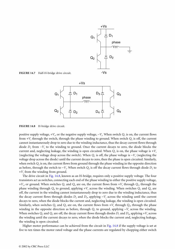
positive supply voltage, +Vs, or the negative supply voltage, −Vs. When switch Q1 is on, the current flowsfrom +Vs through the switch, through the phase winding to ground. When switch Q1 is off, the currentcannot instantaneously drop to zero due to the winding inductance, thus the decay current flows throughdiode D2 from −Vs to the winding to ground. Once the current decays to zero, the diode blocks thecurrent and, neglecting leakage, the winding is open circuited. When Q1 is on, the phase voltage is +Vs
(neglecting the voltage drop across the switch). When Q1 is off, the phase voltage is −Vs (neglecting thevoltage drop across the diode) until the current decays to zero, then the phase is open circuited. Similarly,when switch Q2 is on, the current flows from ground through the phase winding in the opposite directionas before, through the switch to −Vs. When switch Q2 is off the decay current flows through diode D1 to+Vs from the winding from ground.
The drive circuit in Fig. 14.8, known as an H-bridge, requires only a positive supply voltage. The fourtransistors act as switches, connecting each end of the phase winding to either the positive supply voltage,+Vs, or ground. When switches Q1 and Q4 are on, the current flows from +Vs through Q1, through thephase winding through Q4 to ground, applying +Vs across the winding. When switches Q1 and Q4 areoff, the current in the winding cannot instantaneously drop to zero due to the winding inductance, thusthe decay current flows through diodes D2 and D3, applying −Vs across the winding until the currentdecays to zero, when the diode blocks the current and, neglecting leakage, the winding is open circuited.Similarly, when switches Q2 and Q3 are on, the current flows from +Vs through Q3, through the phasewinding in the opposite direction as before, through Q2 to ground, applying −Vs across the winding.When switches Q2 and Q3 are off, the decay current flows through diodes D1 and D4, applying +Vs acrossthe winding until the current decays to zero, when the diode blocks the current and, neglecting leakage,the winding is open circuited.
Higher motor performance can be achieved from the circuit in Fig. 14.8 if the supply voltage is set atfive to ten times the motor rated voltage and the phase currents are regulated by chopping either switch
FIGURE 14.7 Half-H-bridge drive circuit.
FIGURE 14.8 H-bridge drive circuit.
+Vs
-Vs
phase
D1
D2Q2
Q1
+Vs
phaseD1 D3
D2 D4
Q1
Q2
Q3
Q4
© 2002 by CRC Press LLC
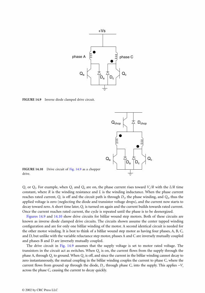
Q1 or Q3. For example, when Q1 and Q4 are on, the phase current rises toward Vs /R with the L/R timeconstant, where R is the winding resistance and L is the winding inductance. When the phase currentreaches rated current, Q1 is off and the circuit path is through D2, the phase winding, and Q4, thus theapplied voltage is zero (neglecting the diode and transistor voltage drops), and the current now starts todecay toward zero. A short time later, Q1 is turned on again and the current builds towards rated current.Once the current reaches rated current, the cycle is repeated until the phase is to be deenergized.
Figures 14.9 and 14.10 show drive circuits for bifilar wound step motors. Both of these circuits areknown as inverse diode clamped drive circuits. The circuits shown assume the center tapped windingconfiguration and are for only one bifilar winding of the motor. A second identical circuit is needed forthe other motor winding. It is best to think of a bifilar wound step motor as having four phases, A, B, C,and D, but unlike with the variable reluctance step motor, phases A and C are inversely mutually coupledand phases B and D are inversely mutually coupled.
The drive circuit in Fig. 14.9 assumes that the supply voltage is set to motor rated voltage. Thetransistors in the circuit act as switches. When Qa is on, the current flows from the supply through thephase A, through Qa to ground. When Qa is off, and since the current in the bifilar winding cannot decay tozero instantaneously, the mutual coupling in the bifilar winding couples the current to phase C, where thecurrent flows from ground up through the diode, Dc , through phase C, into the supply. This applies −Vs
across the phase C, causing the current to decay quickly.
FIGURE 14.9 Inverse diode clamped drive circuit.
FIGURE 14.10 Drive circuit of Fig. 14.9 as a chopperdrive.
+Vs
phase A phase C
QaDa Dc
Qc
Qa
Qchop Dchop
Da Dc
Qc
© 2002 by CRC Press LLC

The drive circuit in Fig. 14.10 works the same way as the drive circuit in Fig. 14.9 when Qchop is on.The addition of Qchop and the additional diode allows the inverse diode clamp drive circuit to be a chopperdrive. The supply voltage is set to five to ten times the motor rated voltage and when either leg of thecircuit is on, the current is regulated using Qchop. When Qchop is off, the phase current drops to half of itsoriginal value, half of the conducting current couples to the opposite phase, and the current flows upthrough the clamp diode in the opposite phase, backward through the opposite phase, through the onphase, and through the on phase transistor.
14.3 Step Motor Models
When a constant current is passed through one phase of a step motor, the motor generates a torque.This torque is typically a sinusoidal function of rotor displacement from the detent position that causesthe rotor to minimize this displacement. When the phases of the motor are excited so that the motor“runs,” the generated torque is still a function of position and current, but the current becomes a varyingquantity, dependent on time, position, velocity, and of course, the drive circuit and drive scheme. Selectionof a motor, drive circuit, and drive scheme depends on predicting the performance and the dynamictorque–speed characteristics of a particular motor with a drive circuit and drive scheme. These perfor-mances of step motors can be predicted to within reasonable accuracy using mathematical models forboth the motor and drive circuit. Ways to model the motor and drive circuit are presented in this section.As with modeling most physical systems, more accurate models produce more accurate results. Tradeoffsbetween accuracy and simplicity are also discussed with each model.
The variable reluctance step motor model needs to be modeled separately from the permanent magnetand hybrid step motor models, and separate models are needed for unifilar and bifilar windings.
Variable Reluctance Step Motor Model
Precise mathematical modeling of variable reluctance step motors requires knowledge of both the geom-etry of the machine and of the ferromagnetic material characteristics. These requirements are oftenrelaxed and assumptions are made to simplify the model to a set of nonlinear differential equations.
Assumption 1. The ferromagnetic material does not saturate. This is a poor assumption for variablereluctance step motors in that the motors are usually operated with a high degree of saturation. Thisassumption is replaced after the “non-saturated” model is presented.
Assumption 2. The inductance for each phase varies sinusoidally around the circumference of the air gap,for example, the phase A inductance is LA(θ ) = L0 + L1 cos(Nrθ ). This assumption required Assumption 1,otherwise LA is a function of both θ and iA.
The terminal voltage for phase A can be found using Faraday’s law as:
(14.3)
where VA is the terminal voltage, RA is the winding resistance, iA is the winding current, and λA is thephase flux linkages. Since λA = LAiA:
(14.4)
where the first term is the magnetizing voltage and the second term is the speed voltage. Equation (14.6)can be rewritten as
(14.5)
VA RAiA
dlA
dt---------+=
dlA
dt-------- LA
diA
dt------- iA
dLA
dt---------+ LA
diA
dt------- L1iAwNr Nrq( )sin–= =
diA
dt-------
1LA
-----VA
RAiA
LA
----------–L1Nr
LA
----------- iAw Nrq( )sin+=
© 2002 by CRC Press LLC

The differential equations for the remaining phases are the same as the above equations, replacing thesubscripts with the appropriate phase letter. The inductances for the other phases, however, need to beshifted in position. For a three-phase motor, the inductances are
(14.6)
For a four-phase motor, the inductances are
(14.7)
The mechanical equations can be found from Newton’s law and conservation of energy. Newton’s lawstates
(14.8)
where J is the rotor and load moment of inertia, ω is the rotor velocity in mechanical radians per second,Te is the torque generated by the motor, TL is the load torque, and B is the rotor and load viscous frictioncoefficient. Using conservation of energy, the torque generated by iA for the variable reluctance step motorassuming no magnetic saturation is
(14.9)
where TA is the torque generated by the current in phase A.Summarizing, the differential equations for the three-phase variable reluctance step motor are
(14.10)
LB q( ) L0 L1 Nrq 2p3
------– cos+=
LC q( ) L0 L1 Nrq 4p3
------– cos+=
LB q( ) L0 L1 Nrq p2---–
cos+=
LC q( ) L0 L1 Nrq p–( )cos+=
LD q( ) L0 L1 Nrq 3p2
------– cos+=
Jdwdt------- Te TL– Bw–=
TA
L1Nr
2----------- Nrq( ) iA
2sin–=
diA
dt-------
1LA
-----VA
RA
LA
------ iA–L1Nr
LA
----------- iAw Nrq( )sin+=
diB
dt-------
1LB
-----VB
RB
LB
------ iB–L1Nr
LB
----------- iBw Nrq 2p3
------– sin+=
diC
dt-------
1LC
-----VC
RC
LC
------ iC–L1Nr
LC
----------- iCw Nrq 4p3
------– sin+=
dwdt-------
Te
J-----
TL
J-----–
BJ---w–=
dqdt------ w=
© 2002 by CRC Press LLC

where
(14.11)
The differential equations for the four-phase variable reluctance step motor are
(14.12)
where
(14.13)
The above model does not account for magnetic saturation of the ferromagnetic material used toconstruct the variable reluctance step motor. A common and effective way to account for the magneticsaturation is to replace the torque expressions with an expression that is linear, instead of quadratic, inphase current. For example, the torque due to the current in phase A is modeled as:
(14.14)
Equation (14.11) is replaced by
(14.15)
Te
L1Nr
2----------- Nrq( )iA
2 Nrq 2p3
------– iB
2sin+sin–=
Nrq 4π3
------– iC
2sin+
diA
dt-------
1LA
-----VA
RA
LA
------ iA–L1Nr
LA
----------- iAw Nrq( )sin+=
diB
dt-------
1LB
-----VB
RB
LB
------ iB–L1Nr
LB
----------- iBw Nrq p2---–
sin+=
diC
dt-------
1LC
-----VC
RC
LC
------ iC–L1Nr
LC
----------- iCw Nrq p–( )sin+=
diD
dt-------
1LD
------VD
RD
LD
------ iD–L1Nr
LD
----------- iDw Nrq 3p4
------– sin+=
dwdt-------
Te
J-----
TL
J-----–
BJ---w–=
dqdt------ w=
Te
L1Nr
2----------- Nrq( )iA
2 Nrq p2---–
iB2sin+sin–=
Nrq p–( )iC2 Nrq 3p
2------–
iD2sin+sin+
TA kT Nrq( ) iAsin–=
Te kT Nrq( ) iA Nrq 2p3
------– iBsin+sin–=
Nrq 4π3
------– iCsin+
© 2002 by CRC Press LLC
and Eq. (14.13) is replaced by
(14.16)
where kT is the torque constant, equal to the zero speed one phase on holding torque.
Bifilar-Wound Hybrid Step Motor Model
A two-phase bifilar-wound hybrid step motor is wound with two windings or one center-tapped windingper pole. A positive current in one center-tapped winding will cause the magnetic flux to align in onedirection, while a positive current in the other half of the winding causes the flux to align in the reversedirection. In both cases, the current can be supplied through the center tap. Thus, this motor can be drivenfrom a single, or unipolar, supply. For convenience, the bifilar-wound hybrid step motor is consideredto have four phases, with each center-tapped winding consisting of two opposite phases. One center-tapped winding consists of phases A and C, the other consists of phases B and D. Nearly perfect fluxcoupling exists between phases A and C as well as between phases B and D, whereas practically no fluxcoupling exists between the two separate winding pairs. As a result, the flux linkage in the kth phase isdue to current in the kth phase winding, the current in the other half of the winding pair, and the fluxdue to the permanent magnet. These relationships are
(14.17)
where λk is the total flux in winding k: λkj is the flux in winding k due to the j current winding and λkf
is the flux in winding k due to the permanent magnet.If the per phase inductances, Lk , are assumed to be equal, i.e., in the kth phase Lk = L for all k, with
the assumption of no saturation, and with eddy currents neglected, the flux linkage due to self-inductanceis λkk = Lik and flux linkage in the opposite ( jth) phase due to mutual inductance is λjk = −λkk where kand j are phases on the same pole. With these relationships between flux linkage and current, Eq. (14.17)reduces to
(14.18)
where λAF, λBF are the flux linkages due to the permanent magnet given by λAF = ko cos(θ) and λBF =ko sin(θ); where ko is the flux constant due to the permanent magnet; θ is the rotor angular position inelectrical radians; and θ = Nrθm, where θm is the mechanical position or displacement of the rotor withrespect to the detent position of phase A which is at θ = 0 rad. Nr is the number of rotor teeth (onemechanical period = Nr electrical period).
Te kT Nrq( )iA Nrq p2---–
iBsin+sin–=
Nrq p–( )iC Nrq 3p2
------– iDsin+sin+
lA lAA lAC lAF+ +=
lB lBB lBD lBF+ +=
lC lA–=
lD lB–=
lA L iA iC–( ) lAF+=
lB L iB iD–( ) lBF+=
© 2002 by CRC Press LLC
The phase voltages, being the voltages measured on the motor terminals, are modeled as
(14.19)
where k = A, B, C, D. RA, RB, RC , and RD represent the resistance of phases A, B, C, and D, respectively,which are not assumed equal, and the super-dot denotes derivative with respect to time.
From Eqs. (14.18) and (14.19), four differential equations corresponding to the four phases can bederived with the flux linkages as the state variables; however, two of these four state variables are dependentsince the flux linkage in phase C is equal to the opposite of that in phase A and flux linkage in phase Dis equal to the opposite of that of phase B, as stated in Eq. (14.17). Only two differential equations arenecessary to model the flux linkages in the motor, one for each half of the motor.
Let the flux linkages in phase A and phase B be the two state variables. Flux linkages are used as statevariables instead of currents because step discontinuities can occur in the current when a phase inswitched, while the flux linkages are continuous in time. For phase A, replacing for iC and iA (for k = A, C)in Eq. (14.18), replacing for λC from Eq. (14.17), and rearranging terms yields
(14.20)
The torque generated by the motor can be modeled by
(14.21)
where
kT = torque constantkm = maximum torque due to the permanent magnet
Drive Circuit Modeling
The easiest and most common way to model a motor and drive circuit is to model the model as presentedabove with all the resistances equal to the phase resistance, and the phase voltages as Vs (or −Vs whenappropriate) when a phase is on and either 0 or −Vs , whichever is appropriate when a phase is off.However, this models the unenergized phases as short circuited, which, after the current has decayed,would be better modeled as an open circuit. In general, this has the effect of underpredicting theperformance of the motor, especially at higher speeds.
When more accurate motor and drive system models are indicated, the phase voltages should be setto Vs , and the transistors and diodes modeled as variable resistors. Conducting transistor and dioderesistances can be set to zero and nonconducting transistor and diode resistances can be set to a large value.
14.4 Control of Step Motors
Successful application of a step motor to a positioning or position tracking application requires carefulattention to the control of the step motor. In this section, techniques are discussed that show how toincrease the torque, double the number of detent positions, and open-loop control characteristics. Thedrive circuits for the various types of step motors and winding configurations was discussed in Section 14.2.
Vk Rkik lk
+=
l˙A
12--VA 1
RA RC–RA RC+------------------–
12--VC 1
RA RC–RA RC+------------------+
RARC lA lAF–( )L RA RC+( )
-------------------------------------––=
l˙B
12--VB 1
RB RD–RB RD+------------------–
12--VD 1
RB RD–RB RD+------------------+
RBRD lB lBF–( )L RB RD+( )
-------------------------------------––=
TE
kT
L----- lA q( ) lB q( )cos+sin–( ) km 4q( )sin–=
© 2002 by CRC Press LLC
Excitation of Step Motors
Although energizing one phase at a time is the simplest way to control the step motor, greater performancefrom the motor is possible by exciting two phases at a time, or by switching between one phase on andtwo phases on at a time. This latter switching scheme is known as half-stepping.
One Phase-On Excitation: By exciting the phases one at a time, the motor will move from detent positionto detent position, for example, A-B-C-D-A-B-C … for a four-phase motor.
Two Phase-On Excitation: When two phases are energized at a time, the torque curves for the individualphases add. The stable detent position is halfway between the detent positions of the motor when thephases are energized one at a time. By exciting the phases two at a time, the motor will move from the newdetent position to new detent position, for example, AB-BC-CD-DA-AB-BC-CD … for a four-phasemotor, where AB is the position halfway between detent position A and detent position B. Exciting thefour-phase motor with two phases on at a time produces more torque but consumes twice the powerof exciting the motor one phase on at a time. Exciting a three-phase motor with two phases on at a timeproduces no additional torque but also consumes twice the power of exciting the motor one phase onat a time.
Half-Stepping Excitation: Switching the excitation alternately between one phase on and two phaseson is called half-stepping excitation. This mode of operation doubles the number of detent positions ofthe motor, in that all of the one phase on detent positions and all of the two phase on detent positionsare available. For example, by exciting a four-phase motor using half-stepping, the rotor can be made tostep from detent position to detent position such as A, AB-B-BC-C-CD-D-DA-A ….
Open-Loop Control
The most common way to control a step motor is open loop, that is, without position and/or velocityfeedback. Once the motor and drive scheme have been chosen, the step command sequence must bechosen. The following examples illustrate some of the characteristics and hazards of open-loop controlledstep motors.
The One-Step Move: Fig. 14.11a illustrates the position vs. time and Fig. 14.11b illustrates the velocityvs. time for a one-step move achieved by deenergizing phase A and energizing phase B. The characteristicposition overshoot and ringing can be seen from these plots. Figure 14.11c shows the velocity vs. positionor phase–plane plot of this one-step move. Observe that the peak overshoot is almost half a step. Thepeak velocity reaches over 500 steps per second.
A Six-Step Move at a Rate of 50 Steps per Second: Fig. 14.12a shows the position vs. time and Fig. 14.12bshows the velocity vs. time for a six-step move at a rate of 50 steps per second. The stair step in Fig. 14.12ais the commanded position, the straight line in Fig. 14.12b is commanded velocity. We can see the motoris moving in discrete steps, in that the position and velocity profiles are almost six individual single-stepresponses with overshoots close to half a step and peak velocities over 500 steps per second and close to−400 steps per second.
A Six-Step Move at a Rate of 500 Steps per Second: Fig. 14.13a shows the position vs. time andFig. 14.13b shows the velocity vs. position for a six-step move at a rate of 500 steps per second. The stairstep in Fig. 14.13a is the commanded position and the straight line in Fig. 14.13b is the commandedvelocity. In these figures, we no longer see the individual step responses in that the next phase is energizedbefore the rotor has reached the peak overshoot for the previously energized phase. The velocity profileshows that the motor is still not running at a constant speed, but the wild velocity oscillations are gone.The characteristic ringing is seen at the end of the move.
A Six-Step Move at a Rate of 1000 Steps per Second: Fig. 14.14a shows the position vs. time andFig. 14.14b shows the velocity vs. position for a six-step move at a rate of 1000 steps per second. The stairstep in Fig. 14.14a is the commanded position and the straight line in Fig. 14.14b is the commandedvelocity. In these figures, we see that the rotor is unable to keep up with the commanded position. A stepmotor is a synchronous machine, and can generate nonzero average torque only at synchronous speed.
2
© 2002 by CRC Press LLC
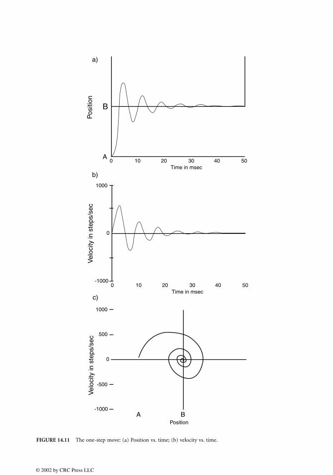
FIGURE 14.11 The one-step move: (a) Position vs. time; (b) velocity vs. time.
B
a)
b)
c)
Pos
ition
A0 10 20 30 40 50
Time in msec
0 10 20 30 40 50Time in msec
1000
0
-1000
-1000
1000
-500
500
0
PositionA B
Vel
ocity
in s
teps
/sec
Vel
ocity
in s
teps
/sec
© 2002 by CRC Press LLC
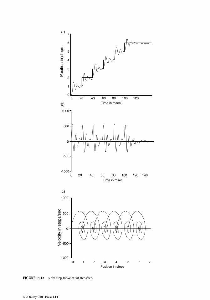
FIGURE 14.12 A six-step move at 50 steps/sec.
00
1
2
3
4
5
6
7
20 40 60 80 100 120Time in msec
0 20 40 60 80 100 120 140
Time in msec
a)
b)
1000
-1000
500
-500
c)
1000
-1000
500
0
-500
0
Position in steps0 1 2 3 4 5 6 7
Pos
ition
in s
teps
Vel
ocity
in s
teps
/sec
© 2002 by CRC Press LLC
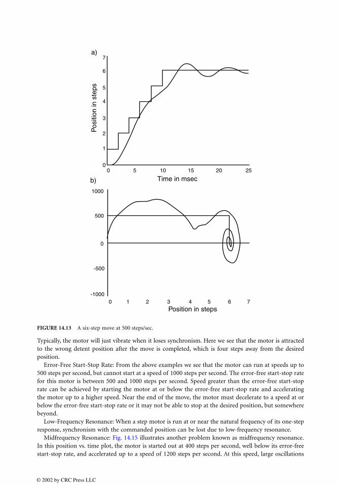
Typically, the motor will just vibrate when it loses synchronism. Here we see that the motor is attractedto the wrong detent position after the move is completed, which is four steps away from the desiredposition.
Error-Free Start-Stop Rate: From the above examples we see that the motor can run at speeds up to500 steps per second, but cannot start at a speed of 1000 steps per second. The error-free start-stop ratefor this motor is between 500 and 1000 steps per second. Speed greater than the error-free start-stoprate can be achieved by starting the motor at or below the error-free start-stop rate and acceleratingthe motor up to a higher speed. Near the end of the move, the motor must decelerate to a speed at orbelow the error-free start-stop rate or it may not be able to stop at the desired position, but somewherebeyond.
Low-Frequency Resonance: When a step motor is run at or near the natural frequency of its one-stepresponse, synchronism with the commanded position can be lost due to low-frequency resonance.
Midfrequency Resonance: Fig. 14.15 illustrates another problem known as midfrequency resonance.In this position vs. time plot, the motor is started out at 400 steps per second, well below its error-freestart-stop rate, and accelerated up to a speed of 1200 steps per second. At this speed, large oscillations
FIGURE 14.13 A six-step move at 500 steps/sec.
00
1
2
3
4
5
6
7
5 10 15 2520
Time in msec
Pos
ition
in s
teps
Position in steps0 1 2 3 4 5 6 7
1000
-1000
500
0
-500
a)
b)
© 2002 by CRC Press LLC
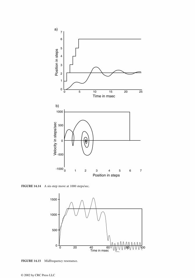
FIGURE 14.14 A six-step move at 1000 steps/sec.
FIGURE 14.15 Midfrequency resonance.
00
1
2
3
4
5
6
7
5 10 15 2520
Time in msec
Pos
ition
in s
teps
Position in steps
Vel
ocity
in s
teps
/sec
0 1 2 3 4 5 6 7
1000
-1000
500
0
-500
a)
b)
Time in msec0 20 40 60 80 100
0
500
1000
1500
© 2002 by CRC Press LLC

occur in the velocity until, finally, the rotor loses synchronism with the commanded signal. This phe-nomenon can be avoided by accelerating through this speed range.
References
Kuo, B. C., Ed. 1979. Incremental Motion Control, Vols. 1 and 2, SRL Publishing Co., Champaign, IL.Leenhouts, A. C. 1986. The Art and Practice of Step Motor Control, Intertec Communications, Ventura, CA.Miller, T. J. E. 1993. Switched Reluctance Motors and Their Control, Oxford University Press, Oxford, U.K.
© 2002 by CRC Press LLC

15Servo Drives
15.1 DC Drives15.2 Induction Motor Drives
PM Synchronous Motor Drive
A significant and very special class of industrial drives are those that are used for position control. Thesedrives are typically called servo drives and the intelligent control of these drives is often called motioncontrol. Some of the application areas of servo drives are machine tool servos, robotic actuator drives,electric vehicles, computer disk drives and the like. The power level for these drives usually range below20 to 30 kW; however, drives with slightly lower control quality usually have power levels below 50 to60 kW.
Servo drives must meet several quality requirements, such as:
1. High dynamic response, which can be realized only with special control schemes and specialmotors with a high torque/inertia torque ratio
2. Smooth torque production in order to achieve smooth rotation and the elimination of positionangle oscillations
3. High reliability with quick maintenance and repair4. Robust control, i.e., the ability of the drives to tolerate wide swings in load inertia or motor
parameters
As a result of these quality requirements, the price of servo drives can be several times that of commonindustrial drives of the same size.
The control scheme for servo drives usually consists of three subordinate loops as shown in Fig. 15.1.The first and most inner one is the current control loop. The YI transfer function of the current controlleris generally chosen in such a manner that the current closed loop must have a cutoff angular frequencyof ω 0I ≥ 1000 r/s. The second control loop, referred to as the speed loop, usually has a closed-loop controlband width of ω0ω ≥ 300 r/s. The outer loop, or position control loop, must accurately follow the positionreference. All the control loops, as a rule, are proportional integral (PI) controllers; the position controlleris the only one that often employs proportional, sometimes proportional differential controller. But ifa parameter of the system changes in some reasonable fashion, e.g., the inertia torque in a roboticsapplication, this control system cannot achieve fast and accurate position control without overshoot. Inthis case, other types of control schemes have been used such as feed-forward, optimal, and sliding modecontrol.
In some applications the servo drives require only torque control for positioning, e.g., in roboticsapplications. In this case, the torque control loop becomes the outer loop. For most drives a proportion-ality exists between torque and motor current; therefore, in this case torque control means current control.All the control loops, at present, usually employ digital control. Only the current loop, at high operatingfrequencies, is sometimes implemented with analog circuits. About 10% of all servo drives are used insingle applications. In machine tools applications, where there are several axes of control, all the servo
Sándor HalászBudapest University of Technology and Economics
© 2002 by CRC Press LLC
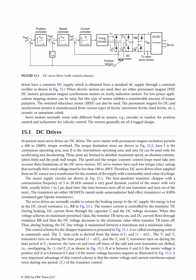
drives have a common DC supply, which is obtained from a standard AC supply through a commonrectifier as shown in Fig. 15.1 When electric motors are used, they are either permanent magnet (PM)DC motors, permanent magnet synchronous motors or, rarely, induction motors. For low-power appli-cations stepping motors can be used, but this type of motor exhibits a considerable amount of torquepulsation. The switched reluctance motor (SRM) can also be used. The permanent magnet for DC andsynchronous motors is manufactured from various types of ferrite (strontium ferrite, hard ferrite, etc.),ceramic or samarium cobalt.
Servo motors normally come with different built-in sensors, e.g., encoder or resolver for positioncontrol and tachometer for velocity control. The motors generally are of a rugged design.
15.1 DC Drives
At present most servo drives are DC drives. The servo motor with permanent magnet excitation permitsa 400 to 1000% torque overload. The torque limitation areas are shown in Fig. 15.2. Area I is thecontinuous operating area; area II is the intermittent operating area; and area III can be used only foraccelerating and decelerating. These areas are limited by absolute maximum speed, an absolute commu-tation limit and the peak stall torque. The speed and the torque (current) control loops must take intoaccount these limitations of the DC servo motors. DC servo motors have such low torque (size) ratingsthat normally their rated voltage must be less than 100 to 200 V. Therefore, DC servo drives when suppliedfrom an AC source use a transformer for the creation of the supply with a reasonably rated value of voltage.
The motor supply circuits are shown in Fig. 15.1. The four-quadrant transistor chopper with acommutation frequency of 5 to 20 kHz ensures a very good dynamic control of the motor with verylittle, usually below 1 to 2 µs, dead time (the time between turn-off of one transistor and turn-on of thenext). The transistors are either MOSFETs (metal oxide semiconductor field effect transistors) or IGBTs(insulated gate bipolar transistors).
The servo drives are normally unable to return the braking energy to the AC supply: the energy is lostin the DC circuit resistance, i.e., RB in Fig. 15.1. The resistor current is controlled by the transistor TB.During braking, DC current flows through the capacitor C and the DC voltage increases. When thisvoltage achieves its maximum permitted value, the transitor TB turns on, and DC current flows throughresistance RB and then the DC voltage decreases to the minimum value when transitor TB turns off.Thus, during braking, the DC line voltage is maintained between a maximum and a minimum value.
The control scheme for the chopper transistors is presented in Fig. 15.3. A so-called overlapping controlis commonly used. The TC time-cycle is derived from the times α TC and (1 − α)TC . The T1 and T4
transistors turn on during the time period (1 − α)TC, and the T2 and T3 transistors turn on during thetime period α TC ; however, the turn-on and turn-off times of the odd and even transistors are shifted,i.e., overlapping, by (1−2α)TC/2 as shown in Fig. 15.3. If α is between 0 and 0.5 the motor voltage ispositive and if α is between 0.5 and 1.0 the motor voltage becomes negative as illustrated in Fig. 15.3. Avery important advantage of this control scheme is that the motor voltage and current waveforms repeattwice during one period (TC) of the transistor control.
FIGURE 15.1 DC servo drive (with control scheme).
Positioncontroller
Positionsensor
-+
-+
+Speed
controllerCurrent
controller
Θref YΘωref Iref
Iω
Yω YIT1
T2RB
C Vdc
T3 T4 TB
DCmotor
To otherservo drives
Θ
AC/DC
Converter
Firingcircuits
M
60 Hz~
© 2002 by CRC Press LLC
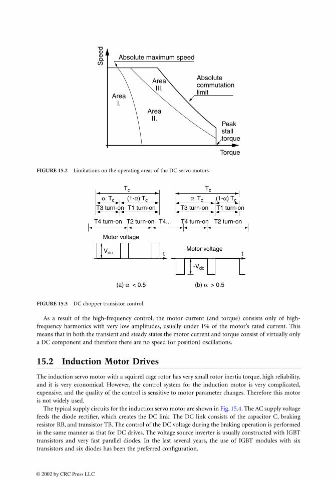
As a result of the high-frequency control, the motor current (and torque) consists only of high-frequency harmonics with very low amplitudes, usually under 1% of the motor’s rated current. Thismeans that in both the transient and steady states the motor current and torque consist of virtually onlya DC component and therefore there are no speed (or position) oscillations.
15.2 Induction Motor Drives
The induction servo motor with a squirrel cage rotor has very small rotor inertia torque, high reliability,and it is very economical. However, the control system for the induction motor is very complicated,expensive, and the quality of the control is sensitive to motor parameter changes. Therefore this motoris not widely used.
The typical supply circuits for the induction servo motor are shown in Fig. 15.4. The AC supply voltagefeeds the diode rectifier, which creates the DC link. The DC link consists of the capacitor C, brakingresistor RB, and transistor TB. The control of the DC voltage during the braking operation is performedin the same manner as that for DC drives. The voltage source inverter is usually constructed with IGBTtransistors and very fast parallel diodes. In the last several years, the use of IGBT modules with sixtransistors and six diodes has been the preferred configuration.
FIGURE 15.2 Limitations on the operating areas of the DC servo motors.
FIGURE 15.3 DC chopper transistor control.
Peakstalltorque
Torque
Absolutecommutationlimit
Absolute maximum speed
AreaI.
AreaII.
AreaIII.
Spe
ed
Motor voltage
Motor voltagett
T4 turn-on
T3 turn-on T3 turn-onT1 turn-on T1 turn-on
T4 turn-onT4...T2 turn-on T2 turn-on
Vdc
Tc
α Tc
(a) α < 0.5 (b) α > 0.5
(1-α) Tc α Tc (1-α) Tc
Tc
-Vdc
© 2002 by CRC Press LLC

The drive does not need a transformer since high-voltage motors are available. If the AC phase voltageis VN (rms value), then the DC link voltage will be and the maximum possible motorphase voltage will be
(15.1)
Hence, if the rated voltage of the motor is equal to the AC supply voltage, then as a result of the voltagedrop in both the rectifier and the inverter, the motor can operate with a rated flux between 0 Hz andthe approximate frequency of the AC supply.
A position control system usually uses the indirect field oriented principle. The rotor flux is generatedby the two phase currents as well as the speed, as shown in Fig. 15.4. The calculation is a function of therotor time constant, which is dependent upon both the rotor resistance and rotor inductance. Variationsin these parameters must be taken into consideration; however, the identification of the parameterchanges is very complicated.
PM Synchronous Motor Drive
The permanent magnet synchronous motor is much more expensive than the squirrel cage inductionmotor, but the control system of the PM synchronous motor drive is much simpler than that used forthe induction motor. When compared to DC motors, PM synchronous motors normally have less inertiatorque and require less maintenance. As a result of these features, the PM synchronous servo drive hasbecome one of the most popular types of servo drives. The converter circuits for PM synchronous motordrives are identical to those for induction motors as shown in Fig. 15.4. PM synchronous motors, suchas induction servo motors, are usually manufactured for high voltage and therefore transformers are notrequired in their use.
There are two classes of PM synchronous motors:
1. Those with a square flux density distribution along the rotor air gap surface, as shown in Fig. 15.5a,which produces a trapezoidal back-emf (electromotive force) in the stator coil—the so-calledtrapezoid PM machines.
2. Those with a sinusoidal flux density distribution, as shown in Fig. 15.5b, which produces asinusoidal back-emf—the so-called sinusoidal PM machines.
In the trapezoidal machines the angle β illustrated in Fig. 15.5a is the width of the magnet. In general,. In Fig. 15.6 the trapezoidal machine with β = 180° is presented and a two-pole machine is
assumed. In steady-state the machine is rotated with constant synchronous speed, which is a functionof the number of pole pairs p and the frequency of the stator supply f1
(15.2)
FIGURE 15.4 Servo drive with induction motor.
Dioderectifier
Voltagesourceinverter
Controlsystem W
Θ reference
Θ
Voltage andfrequency control
CRB
TB
Squirrel-cageinduction
motor
Positionsensor
M3~
ia
Vdc
VN
Vm
ib
~(60 Hz)
+
-
Vdc 3/π 6VN≅
Vm2π---
1
2------- Vdc 3
12
p2--------- VN 1.05VN≅= =
β 180°≅
ω1
2πf1
p---------- const= =
© 2002 by CRC Press LLC
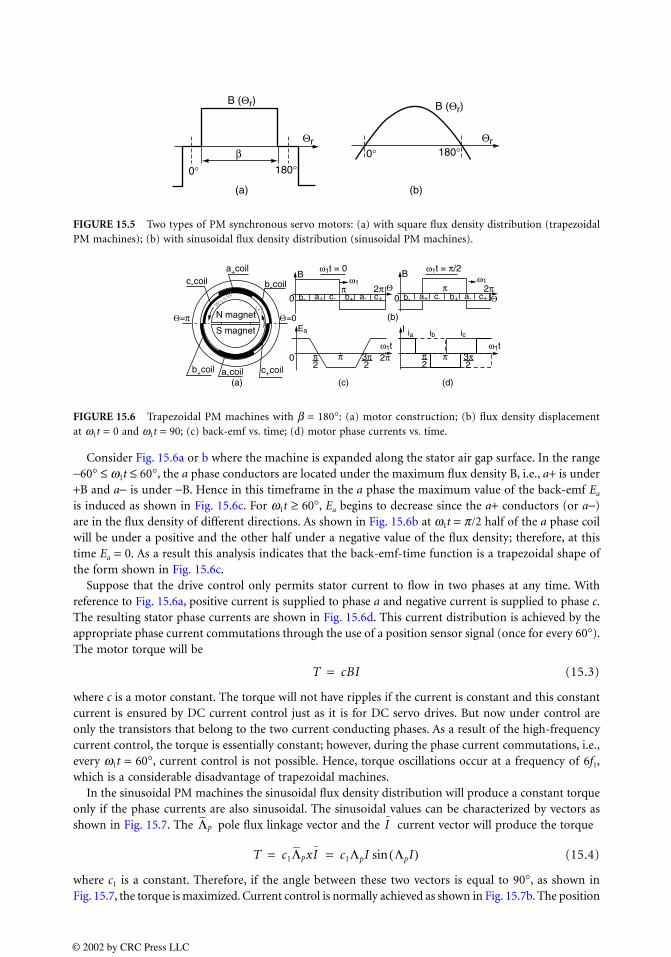
Consider Fig. 15.6a or b where the machine is expanded along the stator air gap surface. In the range−60° ≤ ω1t ≤ 60°, the a phase conductors are located under the maximum flux density B, i.e., a+ is under+B and a− is under −B. Hence in this timeframe in the a phase the maximum value of the back-emf Ea
is induced as shown in Fig. 15.6c. For ω1t ≥ 60°, Ea begins to decrease since the a+ conductors (or a−)are in the flux density of different directions. As shown in Fig. 15.6b at ω1t = π/2 half of the a phase coilwill be under a positive and the other half under a negative value of the flux density; therefore, at thistime Ea = 0. As a result this analysis indicates that the back-emf-time function is a trapezoidal shape ofthe form shown in Fig. 15.6c.
Suppose that the drive control only permits stator current to flow in two phases at any time. Withreference to Fig. 15.6a, positive current is supplied to phase a and negative current is supplied to phase c.The resulting stator phase currents are shown in Fig. 15.6d. This current distribution is achieved by theappropriate phase current commutations through the use of a position sensor signal (once for every 60°).The motor torque will be
(15.3)
where c is a motor constant. The torque will not have ripples if the current is constant and this constantcurrent is ensured by DC current control just as it is for DC servo drives. But now under control areonly the transistors that belong to the two current conducting phases. As a result of the high-frequencycurrent control, the torque is essentially constant; however, during the phase current commutations, i.e.,every ω1t = 60°, current control is not possible. Hence, torque oscillations occur at a frequency of 6f1,which is a considerable disadvantage of trapezoidal machines.
In the sinusoidal PM machines the sinusoidal flux density distribution will produce a constant torqueonly if the phase currents are also sinusoidal. The sinusoidal values can be characterized by vectors asshown in Fig. 15.7. The pole flux linkage vector and the current vector will produce the torque
(15.4)
where c1 is a constant. Therefore, if the angle between these two vectors is equal to 90°, as shown inFig. 15.7, the torque is maximized. Current control is normally achieved as shown in Fig. 15.7b. The position
FIGURE 15.5 Two types of PM synchronous servo motors: (a) with square flux density distribution (trapezoidalPM machines); (b) with sinusoidal flux density distribution (sinusoidal PM machines).
FIGURE 15.6 Trapezoidal PM machines with β = 180°: (a) motor construction; (b) flux density displacementat ω1t = 0 and ω1t = 90; (c) back-emf vs. time; (d) motor phase currents vs. time.
(a)
0° 180°0° 180°
(b)
B (Θr)
Θr Θr
B (Θr)
β
B B
0
02 2
0
(b)I
b-coil
a-coil
c-coila+coil
b+coil c+coil
c- c+a+ a-b-w1=
w b+
ω1
ω1t = 0
ω1t ω1t
ω1t = π/2ω1
c- c+a+ a-b-
iaEa ib ic
b+
N magnet
S magnet
(a) (c) (d)
π π3π 2π
2π Θ
Θ=0(-)
Θ=π
Θ2ππ π
π2π
23π
T cBI=
Λp I
T c1ΛpxI c1ΛpI ΛpI( )sin= =
© 2002 by CRC Press LLC

sensor signal requires the creation of three sinusoidal phase current reference signals, which generate thecurrent vector with a 90° displacement from the pole flux vector. The three Schmidt triggers ensure two-point phase current control with the desired hysteresis. Because the phase current hysteresis is very smallthe motor torque ripples are very high frequency and have very small values. The important advantageof sinusoidal machine drives is that there are no torque oscillations with 6f1 frequency, as is the case withtrapezoidal machines.
References
Jahns, T. M. 1994. Motion control with permanent-magnet AC machines, Proc. IEEE, 82(8), 1241–1255,August, special issue.
Kenjo, T. and Nagamori, S. 1985. PM and Brushless DC Motors, Clarendon Press, Oxford, U.K.Miller, T. J. E. 1993. Brushless Permanent-Magnet and Reluctance Motor Drive, Clarendon Press, Oxford,
U.K.
FIGURE 15.7 Sinusoidal PM machines: (a) pole flux and current vector orientation; (b) control schemes.
Rotor speed and position
Referencecurrent
calculator
(b)(a)
S
N
q
d
c ph
ase
b ph
ase
a ph
ase
tran
sist
or c
ontr
ol
Θ=Θpω1=ω
ω1t = π/2
Irefsin ω1t
ia
ib
ic
Iref
I-
ωref
ωYω
Iref sin (ω1t-1200)900
Iref sin (ω1t-1200)
+
+
+
+
--
-
-
αp
© 2002 by CRC Press LLC

16UninterruptiblePower Supplies
16.1 UPS FunctionsPower Conditioning • System Integration
16.2 Static UPS TopologiesDouble-Conversion UPS • Line-Interactive UPS • Standby Power Supplies
16.3 The Rotary UPS16.4 Alternate AC and DC Sources
Batteries • DC Generators • Superconducting Magnetic Energy Storage • AC Generators
With the proliferation of electronic loads such as computers, the incidence of power quality-relatedproblems is growing. As a result, the uninterruptible power supply (UPS) market has grown significantlyin the last few years. What follows is an overview of UPS functions and descriptions of common typesof UPSs and backup power sources.
16.1 UPS Functions
The primary purpose of a UPS is to provide conditioned, continuous power to its load. Another UPSfunction that is of growing importance in today’s market is system integration, or the ability to commu-nicate over a network to facilitate the monitoring and orderly shutdown of loads.
Power Conditioning
A UPS provides continuous, regulated power to its load, under all conditions of the utility power line.Unlike other types of power conditioning equipment, a UPS provides power during outages. Typically,a UPS will provide backup power for 10 or 15 min, although longer times are possible with large batterystrings or a DC generator.
A UPS will also correct for high- and low-voltage events, known as surges and sags. This regulationis provided either electronically or by a tapped transformer or a ferroresonant transformer.
Normal mode, or line-to-line, transients are prevented from reaching the load. This is accomplishedeither with filter components, or in a double conversion UPS, by converting the AC to DC and then backto AC. There is quite some variation in the ability of UPS systems to protect the load from commonmode, or line-to-ground, transients. Safety agency requirements preclude most forms of common modetransient protection. The best common mode transient suppression is achieved with an isolation trans-former. Some UPSs have isolation transformers and some do not.
Laura SteffekBest Power
John HecklesmillerBest Power
Dave Layden Best Power
Brian YoungBest Power
© 2002 by CRC Press LLC
System Integration
The industrial electronics environment is very similar to the typical office LAN/WAN environment whenit comes to using a UPS to provide power protection for industrial-grade PCs, PLCs and other equipmentthat make use of any form of microprocessor control.
The fact that a UPS only provides a finite amount of battery backup during an extended power outageshould encourage us to take certain precautions to prevent the corruption and loss of data once the UPSreaches a point where it can no longer support the load equipment.
Certain methods may be used to communicate to the load equipment when a power outage has occurredand, in extreme cases, when a low battery condition exists. The load equipment should be configured toreact to critical UPS conditions by saving data and preparing the system for a safe shutdown. Creatingthis “communication” between UPS and the load equipment is called UPS integration. There are severalways that the UPS can be integrated. These methods may be classified into three integration categories:
BasicEnhancedNetwork
No matter what integration methodology is utilized, four items are required to integrate the UPS.First, the UPS must have a communication port. Second, the equipment being protected must also havea communication port. Third, some medium (cabling) must be used to connect the two together. Finally,some form of software must be used to monitor the UPS and provide the appropriate actions relevantto specific UPS conditions.
Basic
The first and most common integration method communicates the status of the UPS via contact closures.Typically, normally open or normally closed relay contacts are used to signal two UPS conditions to theload equipment. These conditions are “AC Failure” and “Low Battery.” An “AC Failure” should be signaledby the UPS whenever a power failure condition exists for more than 5 sec. The “Low Battery” signal existswhen a minimum of 2 min of battery runtime remains to support the load. However, most UPS manu-facturers allow this setpoint to be programmed by the user to allow more time to shutdown the system.
In most cases, the software to monitor the UPS is provided as a part of the computer’s operatingsystem. The UPS manufacturer typically provides the cable and appropriate setup information requiredto connect the two together.
Note that UPS manufacturers often substitute open-collector type circuits in place of actual relays, toprovide the UPS signals. Users should pay close attention to this detail if they choose to build their owninterface cable, since current is only allowed to pass in one direction through an open-collector circuit.
Enhanced
To provide more than just the basic UPS status information, many UPS manufacturers have chosen tooffer RS232 and other forms of serial communication that allow real-time UPS data to be monitored bysoftware running on the load equipment. Instead of knowing only that a power failure has occurred orthat a low battery condition exists, the user may now know how much calculated runtime is availableand the measured battery voltage at any given time. Other data values are typically available that representthe input and output voltage, percent of full load, UPS temperature, as well as many others.
Since the way this UPS data is presented is usually proprietary, the UPS manufacturer most oftensupplies the software to run on the protected load. Because the software is capable of monitoring realtime data from the UPS, a GUI (graphical user interface) is typically used to portray the data using easy-to-read digital displays and historical graphs.
Network
The size and complexity of today’s local and wide area networks has led to an increase in the use ofnetwork management tools to monitor and control network devices. The Simple Network ManagementProtocol (SNMP) has become the de facto standard for network management and is backed by many
© 2002 by CRC Press LLC

network management software products including SunNet Manager, HP-Open View, IBM’s Netview/6000,and Novell’s NMS.
Today, many UPS manufacturers offer software or a software/hardware combination that effectivelymakes the UPS a network peripheral. In some cases an internal or external network adapter is providedthat through its own microprocessor and associated components effectively translates proprietary UPSdata and commands into a format that is compatible with the SNMP standards set forth by a workinggroup of the Internet Engineering Task Force (IETF). This group recently adopted a standard databaseof UPS-related information, called a Management Information Base (MIB), for all UPS products. Theofficial IETF document that describes this MIB is RFC-1628, which is available on the Internet.
The SNMP-capable UPS provides three basic functions when communicating with a network man-agement station. It responds to “get” requests by replying back to the management console with avalue corresponding to the requested MIB variable. It responds to “set” requests by allowing the UPSconfiguration to be changed by the management console. And it broadcasts unsolicited alarm “traps”to the network management console alerting the network administrator to the existence of potentialpower problems.
The UPS in an industrial environment presents a new challenge to the integrator due to the existenceof many different industrial network protocols. In some cases, many of the same protocols exist thatare present in the office LAN environment, but they are often joined by such protocols as SP50 andPROFIBus, which are adaptations of Field Bus. Other industrial control protocols include FIP (FactoryInstrumentation Protocol), MAP (Manufacturing Automation Protocol), and Echelon’s LonTalk. UPSmanufacturers have not yet built in direct connections to these industrial networks. In some cases,protocol adapters are available that translate the RS232 information from the UPS into the requirednetwork protocol. Future developments from UPS vendors may enhance and simplify the UPS connec-tivity in the industrial environment.
16.2 Static UPS Topologies
A static UPS is one that relies on power electronics, rather than a motor generator, to provide power tothe load. Most UPSs today are of this type.
There are several basic UPS topologies, each of which has its advantages and disadvantages. The terms“on-line UPS” and “off-line UPS” have commonly been used to describe some UPS topologies. Unfor-tunately, UPS manufacturers have not been able to agree on the meanings of these terms, leading toconfusion among users. Terms which are more descriptive of the differences between various topologiesare double-conversion UPS, line-interactive UPS, and standby power supply.
Double-Conversion UPS
A double-conversion UPS (Fig. 16.1) first rectifies incoming AC line to a DC voltage, then inverts thatDC voltage to provide an AC output. During normal operation, the rectifier is providing current tocharge the batteries and also to the inverter. The inverter supports the load and provides regulation ofthe output voltage and frequency. In the event that line is lost or deviates from the specified input voltage
FIGURE 16.1 Double-conversion UPS. There is no disruption in output power when the UPS transfers from itsline source to battery power, because the inverter is always operating.
RECTIFIER INVERTER
BATTERY
ACOUTPUT
ACINPUT
© 2002 by CRC Press LLC
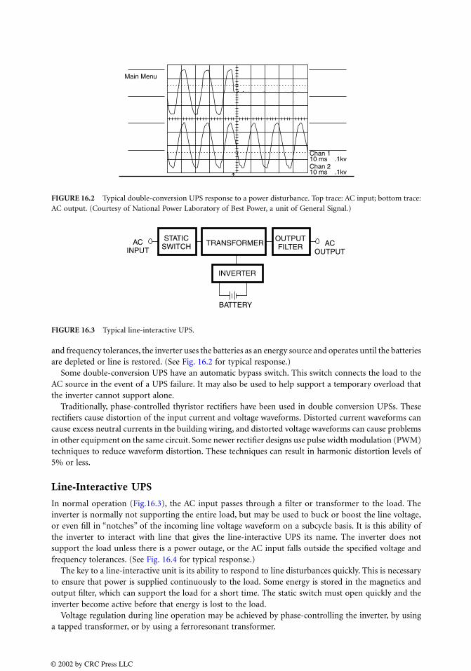
and frequency tolerances, the inverter uses the batteries as an energy source and operates until the batteriesare depleted or line is restored. (See Fig. 16.2 for typical response.)
Some double-conversion UPS have an automatic bypass switch. This switch connects the load to theAC source in the event of a UPS failure. It may also be used to help support a temporary overload thatthe inverter cannot support alone.
Traditionally, phase-controlled thyristor rectifiers have been used in double conversion UPSs. Theserectifiers cause distortion of the input current and voltage waveforms. Distorted current waveforms cancause excess neutral currents in the building wiring, and distorted voltage waveforms can cause problemsin other equipment on the same circuit. Some newer rectifier designs use pulse width modulation (PWM)techniques to reduce waveform distortion. These techniques can result in harmonic distortion levels of5% or less.
Line-Interactive UPS
In normal operation (Fig.16.3), the AC input passes through a filter or transformer to the load. Theinverter is normally not supporting the entire load, but may be used to buck or boost the line voltage,or even fill in “notches” of the incoming line voltage waveform on a subcycle basis. It is this ability ofthe inverter to interact with line that gives the line-interactive UPS its name. The inverter does notsupport the load unless there is a power outage, or the AC input falls outside the specified voltage andfrequency tolerances. (See Fig. 16.4 for typical response.)
The key to a line-interactive unit is its ability to respond to line disturbances quickly. This is necessaryto ensure that power is supplied continuously to the load. Some energy is stored in the magnetics andoutput filter, which can support the load for a short time. The static switch must open quickly and theinverter become active before that energy is lost to the load.
Voltage regulation during line operation may be achieved by phase-controlling the inverter, by usinga tapped transformer, or by using a ferroresonant transformer.
FIGURE 16.2 Typical double-conversion UPS response to a power disturbance. Top trace: AC input; bottom trace:AC output. (Courtesy of National Power Laboratory of Best Power, a unit of General Signal.)
FIGURE 16.3 Typical line-interactive UPS.
Main Menu
Chan 110 ms .1kvChan 210 ms .1kv
STATICSWITCH TRANSFORMER
OUTPUTFILTER
INVERTER
BATTERY
ACINPUT
ACOUTPUT
© 2002 by CRC Press LLC
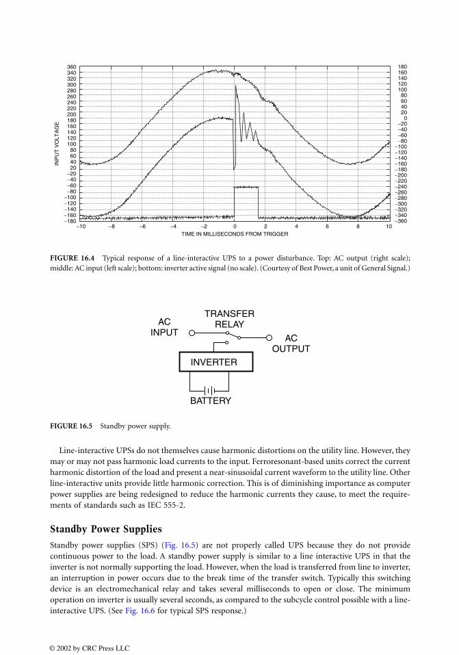
Line-interactive UPSs do not themselves cause harmonic distortions on the utility line. However, theymay or may not pass harmonic load currents to the input. Ferroresonant-based units correct the currentharmonic distortion of the load and present a near-sinusoidal current waveform to the utility line. Otherline-interactive units provide little harmonic correction. This is of diminishing importance as computerpower supplies are being redesigned to reduce the harmonic currents they cause, to meet the require-ments of standards such as IEC 555-2.
Standby Power Supplies
Standby power supplies (SPS) (Fig. 16.5) are not properly called UPS because they do not providecontinuous power to the load. A standby power supply is similar to a line interactive UPS in that theinverter is not normally supporting the load. However, when the load is transferred from line to inverter,an interruption in power occurs due to the break time of the transfer switch. Typically this switchingdevice is an electromechanical relay and takes several milliseconds to open or close. The minimumoperation on inverter is usually several seconds, as compared to the subcycle control possible with a line-interactive UPS. (See Fig. 16.6 for typical SPS response.)
FIGURE 16.4 Typical response of a line-interactive UPS to a power disturbance. Top: AC output (right scale);middle: AC input (left scale); bottom: inverter active signal (no scale). (Courtesy of Best Power, a unit of General Signal.)
FIGURE 16.5 Standby power supply.
−10 −8 −6 −4 −2−360−340−320−300−280−260−240−220−200−180−160−140−120−100
−80
−40−60
−200
20406080
100120140160180
−180−160−140−120−100
−80−60−40−20
20406080
100120140160180200220240260280300320340360
0 2 4 6 8 10TIME IN MILLISECONDS FROM TRIGGER
INP
UT
VO
LTA
GE
ACINPUT
TRANSFERRELAY
ACOUTPUT
INVERTER
BATTERY
© 2002 by CRC Press LLC
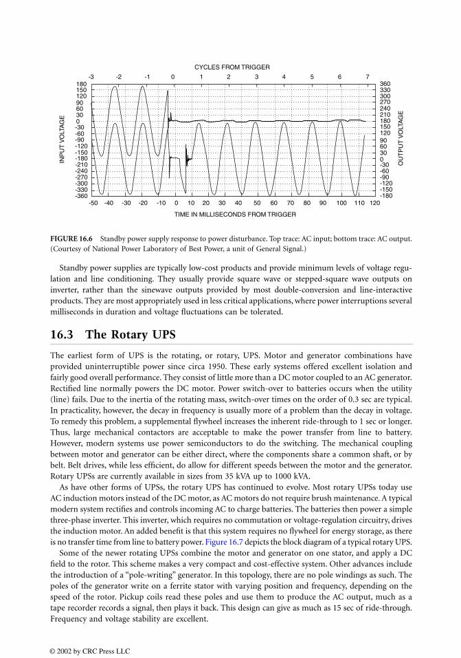
Standby power supplies are typically low-cost products and provide minimum levels of voltage regu-lation and line conditioning. They usually provide square wave or stepped-square wave outputs oninverter, rather than the sinewave outputs provided by most double-conversion and line-interactiveproducts. They are most appropriately used in less critical applications, where power interruptions severalmilliseconds in duration and voltage fluctuations can be tolerated.
16.3 The Rotary UPS
The earliest form of UPS is the rotating, or rotary, UPS. Motor and generator combinations haveprovided uninterruptible power since circa 1950. These early systems offered excellent isolation andfairly good overall performance. They consist of little more than a DC motor coupled to an AC generator.Rectified line normally powers the DC motor. Power switch-over to batteries occurs when the utility(line) fails. Due to the inertia of the rotating mass, switch-over times on the order of 0.3 sec are typical.In practicality, however, the decay in frequency is usually more of a problem than the decay in voltage.To remedy this problem, a supplemental flywheel increases the inherent ride-through to 1 sec or longer.Thus, large mechanical contactors are acceptable to make the power transfer from line to battery.However, modern systems use power semiconductors to do the switching. The mechanical couplingbetween motor and generator can be either direct, where the components share a common shaft, or bybelt. Belt drives, while less efficient, do allow for different speeds between the motor and the generator.Rotary UPSs are currently available in sizes from 35 kVA up to 1000 kVA.
As have other forms of UPSs, the rotary UPS has continued to evolve. Most rotary UPSs today useAC induction motors instead of the DC motor, as AC motors do not require brush maintenance. A typicalmodern system rectifies and controls incoming AC to charge batteries. The batteries then power a simplethree-phase inverter. This inverter, which requires no commutation or voltage-regulation circuitry, drivesthe induction motor. An added benefit is that this system requires no flywheel for energy storage, as thereis no transfer time from line to battery power. Figure 16.7 depicts the block diagram of a typical rotary UPS.
Some of the newer rotating UPSs combine the motor and generator on one stator, and apply a DCfield to the rotor. This scheme makes a very compact and cost-effective system. Other advances includethe introduction of a “pole-writing” generator. In this topology, there are no pole windings as such. Thepoles of the generator write on a ferrite stator with varying position and frequency, depending on thespeed of the rotor. Pickup coils read these poles and use them to produce the AC output, much as atape recorder records a signal, then plays it back. This design can give as much as 15 sec of ride-through.Frequency and voltage stability are excellent.
FIGURE 16.6 Standby power supply response to power disturbance. Top trace: AC input; bottom trace: AC output.(Courtesy of National Power Laboratory of Best Power, a unit of General Signal.)
-50 -40 -30 -20 -10 0 10 20 30 40 50 60 70 80 90 100 110 120
TIME IN MILLISECONDS FROM TRIGGER
-360-330-300-270-240-210-180-150-120-90-60-300306090120150180
-180-150-120-90-60-300306090120150180210240270300330360
-3 -2 -1 0 1 2 3 4 5 6 7
CYCLES FROM TRIGGERIN
PU
T V
OLT
AG
E
OU
TP
UT
VO
LTA
GE
© 2002 by CRC Press LLC
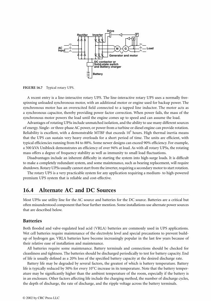
A recent entry is a line-interactive rotary UPS. The line-interactive rotary UPS uses a normally free-spinning unloaded synchronous motor, with an additional motor or engine used for backup power. Thesynchronous motor has an overexcited field connected to a tapped line inductor. The motor acts asa synchronous capacitor, thereby providing power factor correction. When power fails, the mass of thesynchronous motor powers the load until the engine comes up to speed and can assume the load.
Advantages of rotating UPSs include unmatched isolation, and the ability to use many different sourcesof energy. Single- or three-phase AC power, or power from a turbine or diesel engine can provide rotation.Reliability is excellent, with a demonstrable MTBF that exceeds 10
6 hours. High thermal inertia means
that the UPS can sustain very heavy overloads for a short period of time. The units are efficient, withtypical efficiencies running from 84 to 88%. Some newer designs can exceed 90% efficiency. For example,a 500 kVA Uniblock demonstrates an efficiency of over 94% at load. As with all rotary UPSs, the rotatingmass offers a degree of frequency stability as well as immunity to small load fluctuations.
Disadvantages include an inherent difficulty in starting the system into high-surge loads. It is difficultto make a completely redundant system, and some maintenance, such as bearing replacement, will requireshutdown. Rotary UPSs usually cannot start from the inverter, requiring a secondary motor to start rotation.
The rotary UPS is a very practicable system for any application requiring a medium- to high-poweredpremium UPS system that is reliable and cost-effective.
16.4 Alternate AC and DC Sources
Most UPSs use utility line for the AC source and batteries for the DC source. Batteries are a critical butoften misunderstood component that bear further mention. Some installations use alternate power sourcesthat are described below.
Batteries
Both flooded and valve-regulated lead acid (VRLA) batteries are commonly used in UPS applications.Wet cell batteries require maintenance of the electrolyte level and special precautions to prevent build-up of hydrogen gas. VRLA batteries have become increasingly popular in the last few years because oftheir relative ease of installation and maintenance.
All batteries require some maintenance. Battery terminals and connections should be checked forcleanliness and tightness. The batteries should be discharged periodically to test for battery capacity. Endof life is usually defined as a 20% loss of the specified battery capacity at the desired discharge rate.
Battery life may be degraded by several factors, the greatest of which is battery temperature. Batterylife is typically reduced by 50% for every 10°C increase in its temperature. Note that the battery temper-ature may be significantly higher than the ambient temperature of the room, especially if the battery isin an enclosure. Other factors affecting life include the charging method, the number of discharge cycles,the depth of discharge, the rate of discharge, and the ripple voltage across the battery terminals.
FIGURE 16.7 Typical rotary UPS.
ACInput
Rectifer InverterDrive
Battery
Generator and motor
Load
VF
M G
DC contactor orSolid-state switchand Battery charger
© 2002 by CRC Press LLC

Battery storage life is also temperature dependent. Batteries experience a self-discharge at a rate thatincreases with temperature. This self-discharge is in addition to any current drain the UPS may havewhen it is off. UPS batteries should be charged upon receipt and every 6 months of storage after that,or more often if the storage temperature exceeds 25°C. If a battery is stored longer than this withoutbeing recharged, then a phenomenon called sulfation will occur. Sulfation is the formation of lead sulfateon the battery plates. This lead sulfate is an insulator and causes a loss of battery capacity. Many batteryusers have stored their batteries for long periods of time, only to find that at installation those batterieshave no useful capacity at all. Most of the lost capacity can be recovered by exercising the batteries withrepeated charge/discharge cycles, preferably at a high charge rate.
DC Generators
Direct current (DC) power generation has developed over the years to become a viable replacement forbatteries in a variety of applications. These applications range from remote island power, such as railroadsignal and switching, to uninterruptible power system backup and even lighting applications. Anywherebatteries are traditionally used, a DC generator can be installed to reduce the battery requirement orwork in conjunction with alternate power sources such as solar.
To a great extent, the DC generator of today has changed from the days of maintenance-intensivebrushes and commutators to highly efficient rectified systems. Now, instead of relying on the brush andcommutator to perform the rectification process, AC alternators and diodes are used to produce near-“battery quality” DC power. Reduced maintenance requirements through elimination of brushes, com-mutators, and slip rings are a few of the obvious advantages of a solid-state rectified system. Highfrequency alternators and rectifier assemblies provide years of reliable service in less floor space thantraditional AC generators or batteries.
Applications such as railroad switch and signal locations are examples of the versatility of DC powergeneration. Traditionally signal maintenance staff would replace a discharged battery with a rechargedbattery every few days. This was required to keep the trains rolling by properly signaling the track’savailability. Even at sites where solar power sources were utilized, dark days could force increased signalmaintenance due to low battery conditions. DC power generation has successfully demonstrated longterm battery backup and cooperation with other alternate energy sources. Some railroad applicationshave adopted a “cycling duty” system to maintain signal integrity. By allowing the battery to dischargeor the solar charger to operate, a DC generator can be used to automatically start and recharge the batterywhen required. This reduces the site maintenance requirement to about twice a year.
UPS backup applications for DC generation have also proven viable alternatives to large strings ofbatteries. By installing a “minimum” battery, most short-term power outages can be supported. For thelong duration power outages, DC power generation can be used. DC power generation generally requiresonly a connection to the two battery terminals for the system to operate. Through these two batteryconnections the battery condition is monitored and the DC power generator will start and run auto-matically to provide long-term reliable DC power to the UPS inverter. Using the DC generator topology,oversized AC generators are not required. Generally the AC generator manufacturers recommend oversizingthe generator to reduce the power factor induced by many UPS installations. With a DC generator, theinduced power factor problem is not possible.
DC power generation has even grown into the lighting arena. By using a DC power source for floorlighting, HID bulb life is increased substantially. In some cases, this increase can be tenfold. Lightingmanufacturers have doubled their lamp warranties due to DC power. In conjunction with these instal-lations, DC power users have discovered the many utility rebates and rate credits available for peak-shaving with DC power generators. Generator run times as low as 50 hours per year can qualify for utilitypower reduction programs.
Telecommunications applications such as remote offices and cellular radio sites also enjoy the reliabilityof DC power generation. Even the information superhighway is powered by DC generators, bringing thebenefits of the new technology to your doorstep.
Figure 16.8 shows two examples of DC generators available for operation with UPSs.
© 2002 by CRC Press LLC
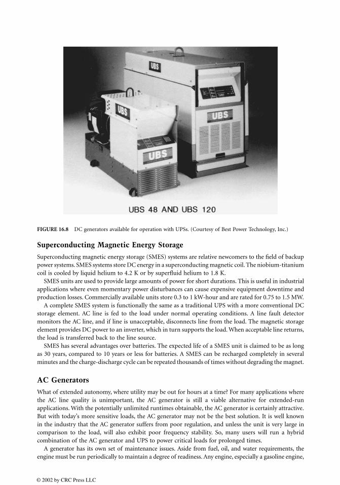
Superconducting Magnetic Energy Storage
Superconducting magnetic energy storage (SMES) systems are relative newcomers to the field of backuppower systems. SMES systems store DC energy in a superconducting magnetic coil. The niobium-titaniumcoil is cooled by liquid helium to 4.2 K or by superfluid helium to 1.8 K.
SMES units are used to provide large amounts of power for short durations. This is useful in industrialapplications where even momentary power disturbances can cause expensive equipment downtime andproduction losses. Commercially available units store 0.3 to 1 kW-hour and are rated for 0.75 to 1.5 MW.
A complete SMES system is functionally the same as a traditional UPS with a more conventional DCstorage element. AC line is fed to the load under normal operating conditions. A line fault detectormonitors the AC line, and if line is unacceptable, disconnects line from the load. The magnetic storageelement provides DC power to an inverter, which in turn supports the load. When acceptable line returns,the load is transferred back to the line source.
SMES has several advantages over batteries. The expected life of a SMES unit is claimed to be as longas 30 years, compared to 10 years or less for batteries. A SMES can be recharged completely in severalminutes and the charge-discharge cycle can be repeated thousands of times without degrading the magnet.
AC Generators
What of extended autonomy, where utility may be out for hours at a time? For many applications wherethe AC line quality is unimportant, the AC generator is still a viable alternative for extended-runapplications. With the potentially unlimited runtimes obtainable, the AC generator is certainly attractive.But with today’s more sensitive loads, the AC generator may not be the best solution. It is well knownin the industry that the AC generator suffers from poor regulation, and unless the unit is very large incomparison to the load, will also exhibit poor frequency stability. So, many users will run a hybridcombination of the AC generator and UPS to power critical loads for prolonged times.
A generator has its own set of maintenance issues. Aside from fuel, oil, and water requirements, theengine must be run periodically to maintain a degree of readiness. Any engine, especially a gasoline engine,
FIGURE 16.8 DC generators available for operation with UPSs. (Courtesy of Best Power Technology, Inc.)
© 2002 by CRC Press LLC

must be run occasionally to keep moving parts lubricated, and fuel must be treated against the formationof varnish or bacterial growth, which can restrict fuel flow. Generators are usually kept outside, so sheltersmust be built and, in many areas, cold-weather starting packages must also be used.
Sometimes, compatibility problems between AC generators and UPSs occur. Double-conversion isusually the most trouble-free of the different topologies of UPSs when used with an AC generator.As the name implies, the power for the double-conversion UPS is converted twice—once from AC toDC (for the batteries) and then from DC back to AC. This scheme assures that no matter what ishappening on the input, the output can be controlled precisely. A line-interactive or single-conversionUPS that typically passes line through to the output must incorporate design features to accommodateAC generator operation. The primary trade-off is the desensitization of the UPS to the fluctuating inputs.Often, generator outputs are far from sinusoidal and rather unstable, so the voltage window in whichthe UPS stays on utility power must be widened. The out-of-frequency window must also be widened,and the tracking capabilities of the phase-locked-loop must be increased. If these alterations are nottaken, protracted inverter runs result, depleting the batteries and thus negating the purpose of the ACgenerator. Needless to say, the output reflects these widened windows. As most modern UPSs can beadjusted to function with an AC generator, the user must assess the impacts of the somewhat diminishedperformance. The vast majority of loads will function acceptably.
References
DeWinkel, C., Losleben, J., and Billman, J. 1993. Recent applications of superconductivity magnet energystorage, Proc. Power Quality Conf., 462–469.
Griffith, D. 1989. Uninterruptible Power Supplies: Power Conditioners for Critical Equipment, Marcel Dekker,New York.
Platts, J. and St. Aubyn, J. D. 1992. Uninterruptible Power Supplies, Peter Peregrinus, Stevanage, Herts.,U.K.
The Institute of Electrical and Electronic Engineers, 1992. IEEE Recommended Practice for Powering andGrounding Sensitive Electronic Equipment (IEEE Emerald Book), IEEE Std. 1100-1992, Institute ofElectrical and Electronic Engineers, New York.
© 2002 by CRC Press LLC

17Power Quality and
Utility Interface Issues
17.1 OverviewHarmonics and IEEE 519 • Surge Voltages and C62.41 • Other Standards Addressing Utility Interface Issues
17.2 Power Quality ConsiderationsHarmonics • What Are Harmonics? • Harmonic Sequence • Where Do Harmonics Come From? • Effects of Harmonics on the System Voltage • Notching • Effects of Harmonics on Power System Components • Conductors • Three-Phase Neutral Conductors • Transformers • Effects of Harmonics on System Power Factor • Power Factor Correction Capacitors • IEEE Standard 519
17.3 Passive Harmonic FiltersPassive Filter Design • Appendix—IEEE Recommended Practices and Requirements for Harmonic Control in Electric Power Systems
17.4 Active Filters for Power ConditioningHarmonic-Producing Loads • Theoretical Approach to Active Filters for Power Conditioning • Classification of Active Filters • Integrated Series Active Filters • Practical Applications of Active Filters for Power Conditioning
17.5 Unity Power Factor RectificationDiode Bridge and Phase-Controlled Rectifiers • Standards for Limiting Harmonic Currents • Definitions of Some Common Terms • Passive Solutions • Active Solutions • Summary
17.1 Overview
Wayne Galli
In the traditional sense, when one thinks of power quality, visions of classical waveforms containing 3rd,5th, and 7th, etc. harmonics appear. It is from this perspective that the IEEE in cooperation with utilities,industry, and academia began to attack the early problems deemed “power quality” in the 1980s. However, inthe last 5 to 10 years, the term power quality has come to mean much more than simple power systemharmonics. Because of the prolific growth of industries that operate with sensitive electronic equipment(e.g., the semiconductor industry), the term power quality has come to encompass a whole realm ofanomalies that occur on a power system. Without much effort, one can find a working group or a standardscommittee at various IEEE meetings in which there is much lively debate on the issue of what power
Wayne GalliSouthwest Power Pool
Timothy L. SkvareninaPurdue University
Badrul H. ChowdhuryUniversity of Missouri–Rolla
Hirofumi AkagiTokyo Institute of Technology
Rajapandian AyyanarArizona State University
Amit Kumar JainUniversity of Minnesota
© 2002 by CRC Press LLC

quality entails and how to define various power quality events. The IEEE Emerald Book (IEEE Standard1100-1999, IEEE Recommended Practice for Power and Grounding Electronic Equipment) defines powerquality as:
The concept of powering and grounding electronic equipment in a manner that is suitable to theoperation of that equipment and compatible with the premise wiring system and other connectedequipment.
The increased use of power electronic devices at all levels of energy consumption has forced the issueof power quality out of abstract discussions of definitions down to the user level. For example, a voltagesag of only a few cycles could cause the variable frequency drives or programmable logic controllers(PLC) on a large rolling mill to “trip out” on low voltage, thereby causing lost production and costingthe company money. The question that is of concern to everyone is, “What initiated the voltage sag?” Itcould have been a fault internal to the facility or one external to the facility (either within a neighboringfacility or on the utility system). In the latter two cases, the owner of the rolling mill will place blameon the utility and, in some cases, seek recompense for lost product.
Another example is the semiconductor industry. This segment of industry has been increasingly activein the investigation of power quality issues, for it is in this volatile industry that millions of dollars canpossibly be lost due to a simple voltage fluctuation that may only last two to four cycles. Issues of powerquality have become such a concern in this industry that Semiconductor Equipment and MaterialsInternational (SEMI), the worldwide trade association for the semiconductor industry, has been workingto produce power quality standards explicitly related to the manufacturing of equipment used withinthat industry.
Two excellent references on the definitions, causes, and potential corrections of power quality issuesare Refs. 1 and 2. The purpose of this section, however, is to address some of the main concerns regardingthe power quality related to interfacing with a utility. These issues are most directly addressed in IEEE519-1992 [3] and IEEE/ANSI C62.41 [4].
Harmonics and IEEE 519
Harmonic generation is attributed to the application of nonlinear loads (i.e., loads that when supplieda sinusoidal voltage do not draw a sinusoidal current). These nonlinear loads not only have the potentialto create problems within the facility that contains the nonlinear loads but also can (depending on thestiffness of the utility system supplying energy to the facility) adversely affect neighboring facilities. IEEE519-1992 [3] specifically addresses the issues of steady-state limits on harmonics as seen at the point ofcommon coupling (PCC). It should be noted that this standard is currently under revision and moreinformation on available drafts can be found at http://standards.ieee.org.
The whole of IEEE 519 can essentially be summarized in several of its own tables. Namely, Tables 10.3through 10.5 in Ref. 3 summarize the allowable harmonic current distortion for systems of 120 V to 69 kV,69.001 kV to 161 kV, and greater than 161 kV, respectively. The allowable current distortion (defined interms of the total harmonic distortion, THD) is a function of the stiffness of the system at the PCC,where the stiffness of the system at the PCC is defined by the ratio of the maximum short-circuit currentat the PCC to the maximum demand load current (at fundamental frequency) at the PCC. Table 11.1in Ref. 3 provides recommended harmonic voltage limits (again in terms of THD). Tables 10.3 and 11.1are of primary interest to most facilities in the application of IEEE 519. The total harmonic distortion(for either voltage or current) is defined as the ratio of the rms of the harmonic content to the rms valueof the fundamental quantity expressed in percent of the fundamental quantity. In general, IEEE 519 refersto this as the distortion factor (DF) and calculates it as the ratio of the square root of the sum of thesquares of the rms amplitudes of all harmonics divided by the rms amplitude of the fundamental alltimes 100%. The PCC is, essentially, the point at which the utility ceases ownership of the equipmentand the facility begins electrical maintenance (e.g., the secondary of a service entrance transformer fora small industrial customer or the meter base for a residential customer).
© 2002 by CRC Press LLC

Surge Voltages and C62.41
Reference 4 is a guide (lowest level of standard) for characterizing the ability of equipment on low-voltagesystems (<1000 V) to withstand voltage surges. This guide provides some practical basis for selectingappropriate test waveforms on equipment. The primary application is for residential, commercial, andindustrial systems that are subject to lightning strikes because of their close proximity (electrically speaking)to unshielded overhead distribution lines. Certain network switching operations may also result in similarvoltage transients being experienced.
Other Standards Addressing Utility Interface Issues
Many power quality standards are at present in existence and are under constant revision. The followingstandards either directly or indirectly address issues with the utility interface and can be applied accord-ingly: IEEE 1159 for the monitoring of power quality events, IEEE 1159.3 for the exchange of measuredpower quality data, IEEE P1433 for power quality definitions, IEEE P1531 for guidelines regardingharmonic filter design, IEEE P1564 for the development of sag indices, IEEE 493 (the Gold Book) forindustrial and commercial power system reliability, IEEE 1346 for guidelines in evaluating componentcompatibility with power systems (this guideline is an attempt to better quantify the CBEMA and ITICcurves), C84.1 for voltage ratings of power systems and equipment, IEEE 446 (the Orange Book) foremergency and standby power systems (this standard contains the so-called power acceptability curves),IEEE 1100 (the Emerald Book), IEEE 1409 for development of guidelines for the application of powerelectronic devices/technologies for power quality improvement on distribution systems, and IEEE P1547for the power quality issues associated with distributed generation resources.
As previously mentioned, the IEEE is not the only organization to continue investigation into theimpacts of nonlinear loads on the utility system. Other organizations such as CIGRE, UL, NEMA, SEMI,IEC, and others all play a role in these investigations.
References
1. IEEE Standards Board, IEEE Recommended Practice for Powering and Grounding Electronic Equipment,IEEE Std. 1100-1999.
2. R. C. Dugan, M. F. McGranaghan, and H. W. Beaty, Electrical Power Systems Quality, McGraw-Hill,New York, 1996.
3. IEEE Standards Board, IEEE Recommended Practices and Requirements for Harmonic Control in Elec-trical Power Systems, IEEE Std. 519-1992.
4. IEEE Standards Board, IEEE Recommended Practice on Surge Voltages in Low-Voltage AC Power Circuits,IEEE Std. C62.41-1991.
17.2 Power Quality Considerations
Timothy L. Skvarenina
Harmonics
In the past, utilities had the responsibility to provide a single-frequency voltage waveform, and for themost part, customers’ loads had little effect on the voltage waveform. Now, however, power electronicsare used widely and create nonsinusoidal currents that contain many harmonic components. Harmoniccurrents cause problems in the power system and for other loads connected to the same portion of thepower system. Because utility customers can now cause electrical problems for themselves and others,the Institute of Electrical and Electronic Engineers (IEEE) developed IEEE Standard 519, which placesthe responsibility of controlling harmonics on the user as well as the utility. This section describes harmonics,their cause, and their effects on the system voltage and components.
© 2002 by CRC Press LLC
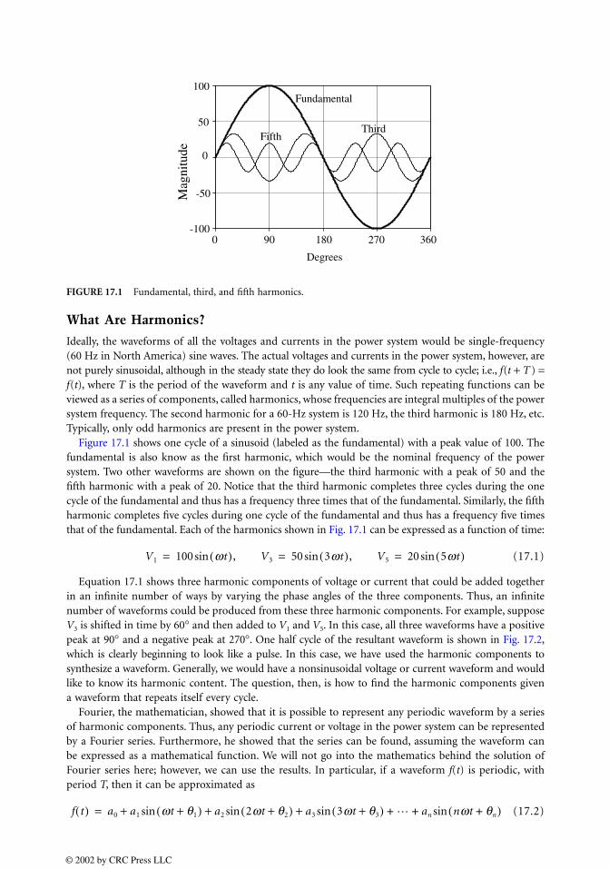
What Are Harmonics?
Ideally, the waveforms of all the voltages and currents in the power system would be single-frequency(60 Hz in North America) sine waves. The actual voltages and currents in the power system, however, arenot purely sinusoidal, although in the steady state they do look the same from cycle to cycle; i.e., f(t + T ) =f(t), where T is the period of the waveform and t is any value of time. Such repeating functions can beviewed as a series of components, called harmonics, whose frequencies are integral multiples of the powersystem frequency. The second harmonic for a 60-Hz system is 120 Hz, the third harmonic is 180 Hz, etc.Typically, only odd harmonics are present in the power system.
Figure 17.1 shows one cycle of a sinusoid (labeled as the fundamental) with a peak value of 100. Thefundamental is also know as the first harmonic, which would be the nominal frequency of the powersystem. Two other waveforms are shown on the figure—the third harmonic with a peak of 50 and thefifth harmonic with a peak of 20. Notice that the third harmonic completes three cycles during the onecycle of the fundamental and thus has a frequency three times that of the fundamental. Similarly, the fifthharmonic completes five cycles during one cycle of the fundamental and thus has a frequency five timesthat of the fundamental. Each of the harmonics shown in Fig. 17.1 can be expressed as a function of time:
(17.1)
Equation 17.1 shows three harmonic components of voltage or current that could be added togetherin an infinite number of ways by varying the phase angles of the three components. Thus, an infinitenumber of waveforms could be produced from these three harmonic components. For example, supposeV3 is shifted in time by 60° and then added to V1 and V5. In this case, all three waveforms have a positivepeak at 90° and a negative peak at 270°. One half cycle of the resultant waveform is shown in Fig. 17.2,which is clearly beginning to look like a pulse. In this case, we have used the harmonic components tosynthesize a waveform. Generally, we would have a nonsinusoidal voltage or current waveform and wouldlike to know its harmonic content. The question, then, is how to find the harmonic components givena waveform that repeats itself every cycle.
Fourier, the mathematician, showed that it is possible to represent any periodic waveform by a seriesof harmonic components. Thus, any periodic current or voltage in the power system can be representedby a Fourier series. Furthermore, he showed that the series can be found, assuming the waveform canbe expressed as a mathematical function. We will not go into the mathematics behind the solution ofFourier series here; however, we can use the results. In particular, if a waveform f(t) is periodic, withperiod T, then it can be approximated as
(17.2)
FIGURE 17.1 Fundamental, third, and fifth harmonics.
-50
50
100
-100
Fundamental
ThirdFifth
Degrees
Mag
nitu
de 0
0 90 180 270 360
V1 100 wt( ), V3sin 50 3wt( ), V5sin 20 5wt( )sin= = =
f t( ) a0 a1 wt q1+( ) a2 2wt q2+( ) a3 3wt q3+( ) … an nwt qn+( )sin+ +sin+sin+sin+=
© 2002 by CRC Press LLC

where a0 represents any DC (average) value of the waveform, a1 through an are the Fourier amplitudecoefficients, and θ1 through θn are the Fourier phase coefficients. The amplitude coefficients are alwayszero or positive and the phase coefficients are all between 0 and 2π radians. As “n” gets larger, theapproximation becomes more accurate.
For example, consider an alternating square wave of amplitude 100. The Fourier series can be shownto be
(17.3)
Since the alternating waveform has zero average value, the coefficient a0 is zero. Note also that only oddharmonics are included in the series given by Eq. (17.3), since (2n − 1) will always be an odd number,and all of the phase coefficients are zero. Expanding the first five terms of Eq. (17.3) yields:
(17.4)
Figure 17.3 shows one cycle for the waveform represented by the right-hand side of Eq. (17.3). Althoughonly the first five terms of the Fourier series were used in Fig. 17.3, the resultant waveform alreadyresembles a square wave. Harmonics have a number of effects on the power system as will be seen later,but for now we would like to have some way to indicate how large the harmonic content of a waveformis. One such figure of merit is the total harmonic distortion (THD).
Total harmonic distortion can be defined two ways. The first definition, in Eq. (17.5), shows the THDas a percentage of the fundamental component of the waveform, designated as THDF. This is the IEEEdefinition of THD and is used widely in the United States.
(17.5)
In Eq. (17.5), V1rms is the rms of the fundamental component and Vhrms is the amplitude of the harmoniccomponent of order “h” (i.e., the “hth” harmonic) . Although the symbol “V” is used in Eqs. (17.5) to(17.10), the equations apply to either current or voltage. The rms of a waveform composed of harmonics
FIGURE 17.2 Pulse wave formed from the three harmonics in Eq. 17.1 with 60° shift for V3.
Degrees
300 60 90 120 150 1800
40
80
120
160
Mag
nitu
de
Vsquare 1001
2n 1–--------------- 2n 1–( )wt[ ]sin
n=1
∞
∑=
Vsquare 100 wt( ) 13-- 3wt( ) 1
5-- 5wt( ) 1
7-- 7wt( ) 1
9-- 9wt( )sin+sin+sin+sin+sin=
THDF
Vhrms2
h=2
∞
∑V1rms
----------------------- 100%×=
© 2002 by CRC Press LLC

is independent of the phase angles of the Fourier series, and can be calculated from the rms values of allharmonics, including the fundamental:
(17.6)
Because the series in Eq. (17.6) has only one more term (the rms of the fundamental) than the seriesin the numerator of Eq. (17.5), we can also find the total rms in terms of percent THDF.
(17.7)
In the opinion of some, Eq. (17.5) exaggerates the harmonic problem. Thus, another technique is alsoused to calculate THD. The alternate method, designated as THDR, calculates THD as a percentage ofthe total rms instead of the rms of the fundamental. From Eq. (17.7), it is clear that the total rms willbe larger than the rms of the fundamental, so such a calculation will yield a lower value for THD. Thisdefinition is used by the Canadian Standards Association and the IEC:
(17.8)
The value for THDR can be obtained from THDF by multiplying by V1rms and dividing by Vrms.
(17.9)
Substituting Eq. (17.7) into Eq. (17.9) yields another expression for THDR in terms of THDF:
(17.10)
THDR, as given by Eq. (17.8) and (17.10), will always be less than 100%. THD is very importantbecause the IEEE Standard 519 specifies maximum values of THD for the utility voltage and the
FIGURE 17.3 Approximation to a square wave using the first five terms of the Fourier series.
Degrees
0 90 270180
0
-100
100
Mag
nitu
de
360
Vrms Vhrms2
h=1
∞
∑=
Vrms V1rms 1%THDF
100-------------------
2
+=
THDR
Vhrms2
h=2
∞
∑Vrms
----------------------- 100%×=
THDR THDF
I1rms
Irms
---------- ×=
THDR
THDF
1%THDF
100--------------------
2
+
-----------------------------------------=
© 2002 by CRC Press LLC
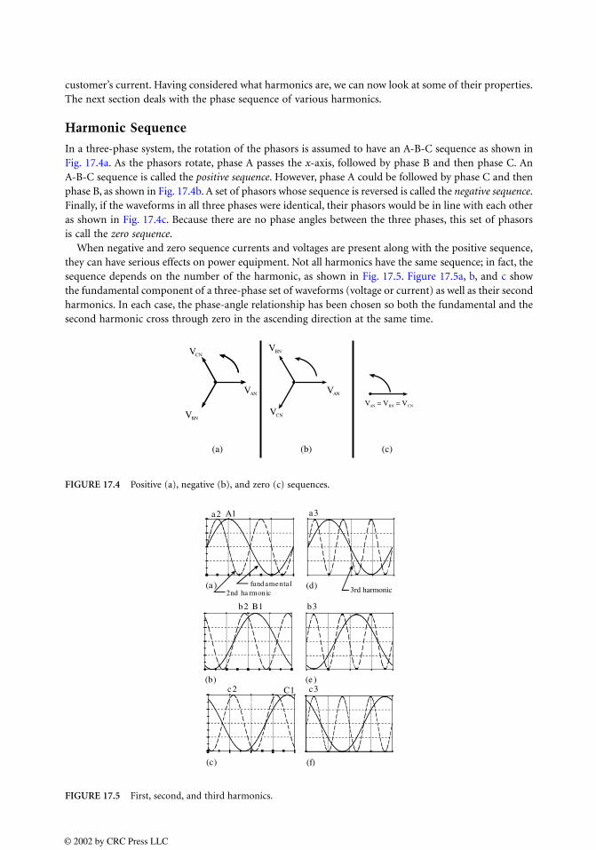
customer’s current. Having considered what harmonics are, we can now look at some of their properties.The next section deals with the phase sequence of various harmonics.
Harmonic Sequence
In a three-phase system, the rotation of the phasors is assumed to have an A-B-C sequence as shown inFig. 17.4a. As the phasors rotate, phase A passes the x-axis, followed by phase B and then phase C. AnA-B-C sequence is called the positive sequence. However, phase A could be followed by phase C and thenphase B, as shown in Fig. 17.4b. A set of phasors whose sequence is reversed is called the negative sequence.Finally, if the waveforms in all three phases were identical, their phasors would be in line with each otheras shown in Fig. 17.4c. Because there are no phase angles between the three phases, this set of phasorsis call the zero sequence.
When negative and zero sequence currents and voltages are present along with the positive sequence,they can have serious effects on power equipment. Not all harmonics have the same sequence; in fact, thesequence depends on the number of the harmonic, as shown in Fig. 17.5. Figure 17.5a, b, and c showthe fundamental component of a three-phase set of waveforms (voltage or current) as well as their secondharmonics. In each case, the phase-angle relationship has been chosen so both the fundamental and thesecond harmonic cross through zero in the ascending direction at the same time.
FIGURE 17.4 Positive (a), negative (b), and zero (c) sequences.
FIGURE 17.5 First, second, and third harmonics.
VAN
VBN
VCN
V = V = VAN BN CN
(a) (b) (c)
VAN
VBN
VCN
(a ) (d)
(b) (e )
(c) (f)
A1
B1
C1
a2
b2
c2
a3
b3
c3
2nd ha rmon icfundamenta l
3rd harmonic
© 2002 by CRC Press LLC

To establish the sequence of the fundamental components, label the positive peak values of the three phasesA1, B1, and C1. Clearly, A1 occurs first, then B1, and finally C1. Thus, we can conclude that the fundamentalcomponent has an A-B-C, or positive, sequence. In fact, it was chosen to have a positive sequence. Giventhat the fundamental has a positive sequence, we can now look at other harmonics. In a similar manner, thefirst peak of each of the second harmonics are labeled a2, b2, and c2. In this case, a2 occurs first, but it isfollowed by c2 and then b2. The second harmonic thus has an A-C-B, or negative, sequence.
Now consider Fig. 17.5d, e, and f, which also show the same fundamental components, but insteadof the second harmonic, the third harmonic is shown. Both the fundamental and third harmonics werechosen so they cross through zvoero together. When the peaks of the third harmonics are labeled as a3,b3, and c3, it is evident that all three occur at the same time. Since the third harmonics are concurrent,they have no phase order. Thus, they are said to have zero sequence. If the process in Fig. 17.5 wascontinued, the fourth harmonic would have a positive sequence, the fifth a negative sequence, the sixtha zero sequence, and so on.
All harmonics whose order is 3n, where n is any positive integer, are zero sequence and are calledtriplen harmonics. Triplen harmonics cause serious problems in three-phase systems as discussed laterin this section. First, however, consider what causes harmonics in the power system.
Where Do Harmonics Come From?
Electrical loads that have a nonlinear relationship between the applied voltages and their currents causeharmonic currents in the power system. Passive electric loads consisting of resistors, inductors, andcapacitors are linear loads. If the voltage applied to them consists of a single-frequency sine wave, thenthe current through them will be a single-frequency sine wave as well. Power electronic equipment createsharmonic currents because of the switching elements that are inherent in their operation. For example,consider a simple switched-mode power supply used to provide DC power to devices such as desktopcomputers, televisions, and other single-phase electronic devices.
Figure 17.6 shows an elementary power supply in which a capacitor is fed from the power systemthrough a full-wave, diode bridge rectifier. The instantaneous value of the AC source must be greaterthan the voltage across the capacitor for the diodes to conduct. When first energized, the capacitor chargesto the peak of the AC waveform and, in the absence of a load, the capacitor remains charged and nofurther current is drawn from the source.
If there is a load, then the capacitor acts as a source for the load. After the capacitor is fully charged, theAC voltage waveform starts to decrease, and the diodes shut off. While the diode is off, the capacitordischarges current to the DC load, which causes its voltage, Vdc, to decrease. Thus, when the AC sourcebecomes larger than Vdc during the next half-cycle, the capacitor draws a pulse of current to restore its charge.
FIGURE 17.6 Simple single-phase switch-mode power supply.
VDCIS
VS
C
© 2002 by CRC Press LLC
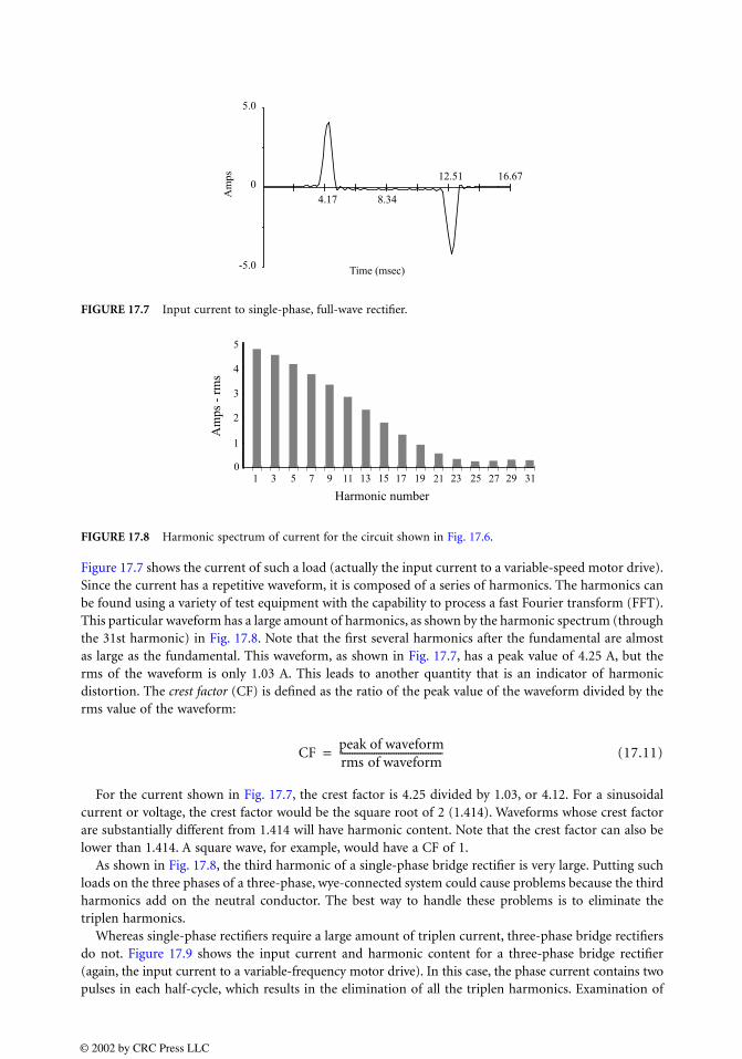
Figure 17.7 shows the current of such a load (actually the input current to a variable-speed motor drive).Since the current has a repetitive waveform, it is composed of a series of harmonics. The harmonics canbe found using a variety of test equipment with the capability to process a fast Fourier transform (FFT).This particular waveform has a large amount of harmonics, as shown by the harmonic spectrum (throughthe 31st harmonic) in Fig. 17.8. Note that the first several harmonics after the fundamental are almostas large as the fundamental. This waveform, as shown in Fig. 17.7, has a peak value of 4.25 A, but therms of the waveform is only 1.03 A. This leads to another quantity that is an indicator of harmonicdistortion. The crest factor (CF) is defined as the ratio of the peak value of the waveform divided by therms value of the waveform:
(17.11)
For the current shown in Fig. 17.7, the crest factor is 4.25 divided by 1.03, or 4.12. For a sinusoidalcurrent or voltage, the crest factor would be the square root of 2 (1.414). Waveforms whose crest factorare substantially different from 1.414 will have harmonic content. Note that the crest factor can also belower than 1.414. A square wave, for example, would have a CF of 1.
As shown in Fig. 17.8, the third harmonic of a single-phase bridge rectifier is very large. Putting suchloads on the three phases of a three-phase, wye-connected system could cause problems because the thirdharmonics add on the neutral conductor. The best way to handle these problems is to eliminate thetriplen harmonics.
Whereas single-phase rectifiers require a large amount of triplen current, three-phase bridge rectifiersdo not. Figure 17.9 shows the input current and harmonic content for a three-phase bridge rectifier(again, the input current to a variable-frequency motor drive). In this case, the phase current contains twopulses in each half-cycle, which results in the elimination of all the triplen harmonics. Examination of
FIGURE 17.7 Input current to single-phase, full-wave rectifier.
FIGURE 17.8 Harmonic spectrum of current for the circuit shown in Fig. 17.6.
5.0
0
-5.0
Am
ps
Time (msec)
4.17 8.34
12.51 16.67
Harmonic number
Am
ps -
rm
s
1 3 5 7 9 11 13 15 17 19 21 23 25 27 29 310
1
2
3
4
5
CFpeak of waveformrms of waveform------------------------------------------=
© 2002 by CRC Press LLC
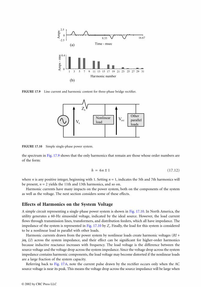
the spectrum in Fig. 17.9 shows that the only harmonics that remain are those whose order numbers areof the form:
(17.12)
where n is any positive integer, beginning with 1. Setting n = 1, indicates the 5th and 7th harmonics willbe present, n = 2 yields the 11th and 13th harmonics, and so on.
Harmonic currents have many impacts on the power system, both on the components of the systemas well as the voltage. The next section considers some of these effects.
Effects of Harmonics on the System Voltage
A simple circuit representing a single-phase power system is shown in Fig. 17.10. In North America, theutility generates a 60-Hz sinusoidal voltage, indicated by the ideal source. However, the load currentflows through transmission lines, transformers, and distribution feeders, which all have impedance. Theimpedance of the system is represented in Fig. 17.10 by Zs. Finally, the load for this system is consideredto be a nonlinear load in parallel with other loads.
Harmonic currents drawn from the power system by nonlinear loads create harmonic voltages (RI +jωh LI) across the system impedance, and their effect can be significant for higher-order harmonicsbecause inductive reactance increases with frequency. The load voltage is the difference between thesource voltage and the voltage drop across the system impedance. Since the voltage drop across the systemimpedance contains harmonic components, the load voltage may become distorted if the nonlinear loadsare a large fraction of the system capacity.
Referring back to Fig. 17.6, note the current pulse drawn by the rectifier occurs only when the ACsource voltage is near its peak. This means the voltage drop across the source impedance will be large when
FIGURE 17.9 Line current and harmonic content for three-phase bridge rectifier.
FIGURE 17.10 Simple single-phase power system.
Harmonic number1 3 5 7 9 11 13 15 17 19 21 23 25 27 29 31A
mps
- r
ms
0
0.4A
mps
0
2.5
-2.5Time - msec
8.33 16.67
(a)
(b)
Other parallelloads
Nonlinearload
Zs
VsVa c
h 6n 1±=
© 2002 by CRC Press LLC
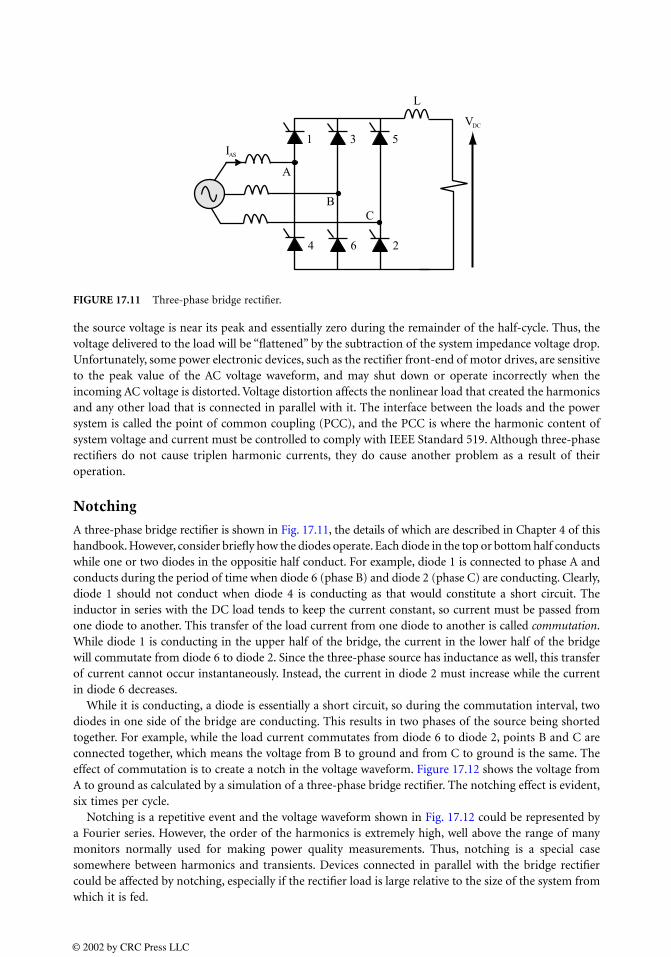
the source voltage is near its peak and essentially zero during the remainder of the half-cycle. Thus, thevoltage delivered to the load will be “flattened” by the subtraction of the system impedance voltage drop.Unfortunately, some power electronic devices, such as the rectifier front-end of motor drives, are sensitiveto the peak value of the AC voltage waveform, and may shut down or operate incorrectly when theincoming AC voltage is distorted. Voltage distortion affects the nonlinear load that created the harmonicsand any other load that is connected in parallel with it. The interface between the loads and the powersystem is called the point of common coupling (PCC), and the PCC is where the harmonic content ofsystem voltage and current must be controlled to comply with IEEE Standard 519. Although three-phaserectifiers do not cause triplen harmonic currents, they do cause another problem as a result of theiroperation.
Notching
A three-phase bridge rectifier is shown in Fig. 17.11, the details of which are described in Chapter 4 of thishandbook. However, consider briefly how the diodes operate. Each diode in the top or bottom half conductswhile one or two diodes in the oppositie half conduct. For example, diode 1 is connected to phase A andconducts during the period of time when diode 6 (phase B) and diode 2 (phase C) are conducting. Clearly,diode 1 should not conduct when diode 4 is conducting as that would constitute a short circuit. Theinductor in series with the DC load tends to keep the current constant, so current must be passed fromone diode to another. This transfer of the load current from one diode to another is called commutation.While diode 1 is conducting in the upper half of the bridge, the current in the lower half of the bridgewill commutate from diode 6 to diode 2. Since the three-phase source has inductance as well, this transferof current cannot occur instantaneously. Instead, the current in diode 2 must increase while the currentin diode 6 decreases.
While it is conducting, a diode is essentially a short circuit, so during the commutation interval, twodiodes in one side of the bridge are conducting. This results in two phases of the source being shortedtogether. For example, while the load current commutates from diode 6 to diode 2, points B and C areconnected together, which means the voltage from B to ground and from C to ground is the same. Theeffect of commutation is to create a notch in the voltage waveform. Figure 17.12 shows the voltage fromA to ground as calculated by a simulation of a three-phase bridge rectifier. The notching effect is evident,six times per cycle.
Notching is a repetitive event and the voltage waveform shown in Fig. 17.12 could be represented bya Fourier series. However, the order of the harmonics is extremely high, well above the range of manymonitors normally used for making power quality measurements. Thus, notching is a special casesomewhere between harmonics and transients. Devices connected in parallel with the bridge rectifiercould be affected by notching, especially if the rectifier load is large relative to the size of the system fromwhich it is fed.
FIGURE 17.11 Three-phase bridge rectifier.
A
3 5
4 6 2
VDC
IAS
BC
1
L
© 2002 by CRC Press LLC
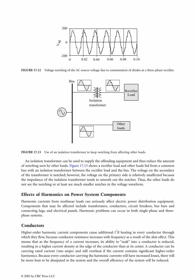
An isolation transformer can be used to supply the offending equipment and thus reduce the amountof notching seen by other loads. Figure 17.13 shows a rectifier load and other loads fed from a commonbus with an isolation transformer between the rectifier load and the bus. The voltage on the secondaryof the transformer is notched; however, the voltage on the primary side is relatively unaffected becausethe impedance of the isolation transformer tends to smooth out the notches. Thus, the other loads donot see the notching or at least see much smaller notches in the voltage waveform.
Effects of Harmonics on Power System Components
Harmonic currents from nonlinear loads can seriously affect electric power distribution equipment.Components that may be affected include transformers, conductors, circuit breakers, bus bars andconnecting lugs, and electrical panels. Harmonic problems can occur in both single-phase and three-phase systems.
Conductors
Higher-order harmonic current components cause additional I2R heating in every conductor through
which they flow, because conductor resistance increases with frequency as a result of the skin effect. Thismeans that as the frequency of a current increases, its ability to “soak” into a conductor is reduced,resulting in a higher current density at the edge of the conductor than at its center. A conductor can becarrying rated current (rms amps) and still overheat if the current contains significant higher-orderharmonics. Because every conductor carrying the harmonic currents will have increased losses, there willbe more heat to be dissipated in the system and the overall efficiency of the system will be reduced.
FIGURE 17.12 Voltage notching of the AC source voltage due to commutation of diodes in a three-phase rectifier.
FIGURE 17.13 Use of an isolation transformer to keep notching from affecting other loads.
Vag
200
0
-2000 0.02 0.04 0.06 0.08 0.10
LoadRectifier
Otherloads
Isolationtransformer
Bus
© 2002 by CRC Press LLC
Three-Phase Neutral Conductors
Triplen harmonics pose a problem for the neutral conductor in three-phase, wye-connected systems,such as the one shown in Fig. 17.14. Therein, a feeder circuit provides three-phase power to a circuitbreaker panel board from which branch circuits provide power to outlets and lighting, including threesingle-phase loads connected via a four-wire branch circuit. When identical linear loads are placed oneach of the three phases, the phase currents add to zero at point “n” and no current flows on the neutralwire. Again assuming linear loads, then even if the load are not identical, the current in the neutral couldnot be higher than the highest phase current.
If the loads in Fig. 17.14 are nonlinear, there will be harmonic currents in each phase. For balancedloads, the fundamentals and all non-triplen harmonic currents add to zero at the neutral point. If triplenharmonics are present in the phase currents, however, they will be in phase and add directly on thebranch circuit and feeder neutrals. Since the neutral conductors carry the sum of the triplens from thethree phases, the neutral current can actually exceed the current in the phase conductors. Since neutralconductors are not protected by circuit breakers, this can damage to the conductors.
To find the current in the neutral, we must recognize that all positive and negative sequence harmonicsfrom the three phases will cancel out at the neutral point. The triplen harmonics, on the other hand,will add together at the neutral:
(17.13)
From Eq. (17.13), it is evident that the neutral current is three times the rms of all the triplens on onephase of the system.
Transformers
Current flow in the windings and flux in the ferromagnetic core cause real power losses in a transformer.Because of their higher frequencies, harmonic currents cause additional losses in every conductor throughwhich they flow, including the conductors of the transformer coils. Harmonic currents in the windingscreate harmonic flux components in the core of the transformer, which cause additional hysteresis andeddy current losses in the steel. Hysteresis loss is proportional to the frequency of the magnetic flux, andeddy currents are proportional to frequency squared. Thus, harmonic currents can cause significant incre-ases in the core loss of the transformer. These additional losses may result in transformer overheatingand electrical insulation failure.
To provide for the effects of nonlinear loads, manufacturers build specially designed transformers,called “K-factor rated,” that are capable of supplying rated output current to loads with a specific level
FIGURE 17.14 Three-phase power system with balanced, single-phase nonlinear loads.
NonlinearLoad
Ia
Ib
Ic
Inn
Three-phasePower Panel
208Y/120 V
4 wirefeedercircuit topanel
NonlinearLoad
NonlinearLoad
INrms 3 I3rms2 I6rms
2 I9rms2 …+ + +( )1/2×=
© 2002 by CRC Press LLC

of harmonic content. K-factor-rated transformers have larger conductors in the windings and thinner,low-loss steel laminations in the core to reduce the losses. A transformer with a K-factor of K-1 is ratedonly for single-frequency current; thus, if the load is nonlinear, the transformer cannot provide ratedcurrent without overheating. Transformers rated K-4, K-9, K-13, and higher are available to providepower to nonlinear loads. K-factors of K-4 or K-9 indicate the transformer can supply rated current toloads that would increase the eddy current loss of a K-1 transformer by a factor of 4 or 9, respectively.Transformers rated K-9 or K-13 would likely be required for office areas containing many desktopcomputers, copy machines, fax machines, and electronic lighting ballasts. A large variable-speed motordrive could require a transformer rated K-30 or higher. The K-factor of a load can be calculated, if theharmonic components are known, as follows:
(17.14)
where h is the harmonic order number, Ih,rms is the rms of the harmonic current whose frequency is “h”times the fundamental frequency, and Itot,rms is the rms of the total current.
Effects of Harmonics on System Power Factor
Earlier, Eq. (17.6) showed that the addition of harmonic currents to the fundamental component increasesthe total rms current. Because they affect the rms value of the current, harmonics will affect the powerfactor of the circuit. Consider the voltage and current waveforms shown in Fig. 17.15 in which currentlags the voltage by an angle θ. The apparent power of the circuit would be found by multiplying the rmsvoltage magnitude by the rms current magnitude. Power factor, Fp, is then defined as the ratio of the realpower to the apparent power:
(17.15)
For linear loads, the phase shift (time displacement) between voltage and current results in differentvalues for real power and apparent power. Since the current can only lag or lead the voltage by 0 to 90°,the power factor will always be positive and less than or equal to 1.
Instead of a sinusoidal current, suppose the current and voltage shown by Fig. 17.16. The current isthe quasi-square wave, consisting of the Fourier series shown in Eq. (17.4). The voltage is a sine wave,
FIGURE 17.15 Voltage and current for a lagging load.
K h2 Ih ,rms
Itot,rms
-------------
2
∑=
FpP
VrmsIrms
------------------ q( )cos= =
Vol
tage
and
cur
rent
Degrees (time)
θV(t)
I(t)
0 90 180 270 360
1
0
-1
© 2002 by CRC Press LLC
which is in phase with the fundamental harmonic component of the current. The power can be foundas a function of time by multiplying the voltage times the current at each time step.
Because the voltage consists of a single component, the power is a series of terms consisting of thevoltage times each harmonic component of current. The first term of the series is of the form sin
2 ωtsince the voltage is in phase with the fundamental current component. Obviously, this term is alwayspositive; therefore, it indicates real power (energy) being delivered to the load.
The remaining terms contain the product of the fundamental frequency voltage and one of the higher-order harmonic current components. Multiplying two sinusoidal waveforms of different frequenciescreates a sinusoidal waveform, which has a zero average value. Thus, none of higher-order harmonic currentsproduces real power if the voltage is a single frequency. Substituting Eq. (17.7) for the total rms currentinto Eq. (17.15) yields a new expression for the power factor:
(17.16)
where the current %THDF is used in the denominator of Eq. (17.16). Rewriting Eq. (17.16):
(17.17)
In Eqs. (17.16) and (17.17), the subscript “tot” indicates the total power factor, which is sometimes calledthe true power factor. The total power factor in Eq. (17.17) is the product of two components, the firstof which is called the displacement power factor:
(17.18)
The second component of the total power factor is the distortion power factor, which results from theharmonic components in the current:
(17.19)
FIGURE 17.16 Sinusoidal voltage and quasi-square wave current.
V(t)
I(t)
Rel
ativ
e m
agni
tude
Degrees (time)0 180 36090 270
1
0
-1
0.5
-0.5
Fp totP
V1rmsIrms
-------------------- P
V1rmsI1rms 1%THDF
100-------------------
2
+
---------------------------------------------------------------= =
Fp totP
V1rmsI1rms
---------------------- 1
1%THDF
100-------------------
2
+
-----------------------------------------×=
FpdispP
V1rmsI1rms
----------------------=
Fp disp1
1%THDF
100-------------------
2
+
-----------------------------------------=
© 2002 by CRC Press LLC
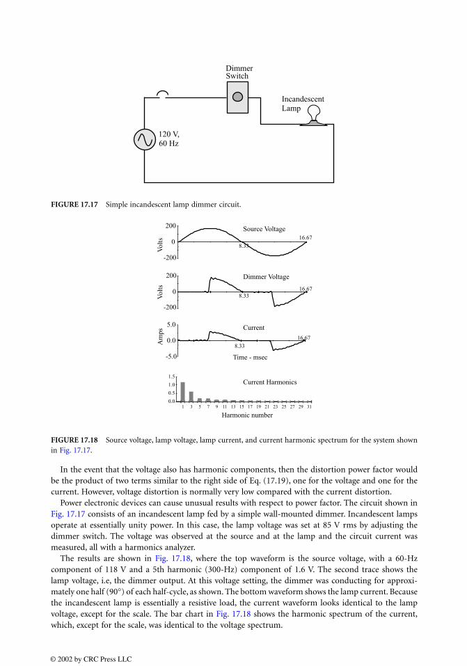
In the event that the voltage also has harmonic components, then the distortion power factor wouldbe the product of two terms similar to the right side of Eq. (17.19), one for the voltage and one for thecurrent. However, voltage distortion is normally very low compared with the current distortion.
Power electronic devices can cause unusual results with respect to power factor. The circuit shown inFig. 17.17 consists of an incandescent lamp fed by a simple wall-mounted dimmer. Incandescent lampsoperate at essentially unity power. In this case, the lamp voltage was set at 85 V rms by adjusting thedimmer switch. The voltage was observed at the source and at the lamp and the circuit current wasmeasured, all with a harmonics analyzer.
The results are shown in Fig. 17.18, where the top waveform is the source voltage, with a 60-Hzcomponent of 118 V and a 5th harmonic (300-Hz) component of 1.6 V. The second trace shows thelamp voltage, i.e, the dimmer output. At this voltage setting, the dimmer was conducting for approxi-mately one half (90°) of each half-cycle, as shown. The bottom waveform shows the lamp current. Becausethe incandescent lamp is essentially a resistive load, the current waveform looks identical to the lampvoltage, except for the scale. The bar chart in Fig. 17.18 shows the harmonic spectrum of the current,which, except for the scale, was identical to the voltage spectrum.
FIGURE 17.17 Simple incandescent lamp dimmer circuit.
FIGURE 17.18 Source voltage, lamp voltage, lamp current, and current harmonic spectrum for the system shownin Fig. 17.17.
120 V, 60 Hz
IncandescentLamp
DimmerSwitch
Current
Time - msec
0.0
5.0
-5.0
. 8.3316.67
Dimmer Voltage
0
200
-200
. 8.3316.67
Source Voltage
0
200
-200
. 8.33
16.67
Harmonic number
0.0
0.5
1.0
1.5
1 3 5 7 9 11 13 15 17 19 21 23 25 27 29 31
Current Harmonics
Vol
tsA
mps
Vol
ts
© 2002 by CRC Press LLC

Since the lamp voltage and current have the same shape and are in phase, the harmonic components ofcurrent and voltage are in phase. With no phase angle between each of the voltage and current components,the power factor of the lamp is unity, and that was found to be the case with the harmonic analyzer.Because the dimmer creates harmonic voltages to the lamp, each harmonic of voltage and its respectivecurrent delivers some power to the lamp at unity power factor.
Looking at the source results in a much different picture. The source voltage consists almost solelyof a single frequency, whereas the current contains all of the harmonics shown in Fig. 17.18. Since theproduct of two sine waves of different frequencies is another sine wave, only the fundamental harmonicof current can deliver real power to the circuit. The harmonics analyzer showed that the fundamentalcomponent of the current lagged the source voltage by 28°. Taking the cosine of 28° results in a measureddisplacement power factor of 0.88 at the source.
THDF for the current was found to be 60.7%, and the distortion power factor was calculated to be0.855 from Eq. (17.19). The product of the distortion power factor and the displacement power factoryields the total power factor, 0.75 in this case. Thus, the incandescent lamp, a resistive load, appears tothe power system as a 0.75 power factor lagging load. Low power factor results in higher losses in thesystem due to higher I
2R losses. In fact, both I and R increase in this case because the rms current is
higher due to the harmonics and because skin effect causes higher resistance in the conductors. While asingle lamp on a dimmer switch does not seriously affect the power system, very large nonlinear loads,such as a DC motor drive, could require the installation of harmonic filters to reduce the distortionpower factor. Passive harmonic filters are briefly described here and in more detail in Section 17.3.
Power Factor Correction Capacitors
Many industrial loads are inductive, so capacitors are often used to improve the power factor. Althoughcapacitors do not cause harmonics, they can resonate with the inductance of the power system. Whenresonant frequencies occur near harmonic frequencies, capacitors can amplify the harmonic currentscreated by nonlinear loads. Figure 17.19 shows a power circuit including power factor correction capac-itors. The parallel combination of the system inductance and the power factor correction capacitors hasa resonant frequency, fr . The resonant frequency is given by
(17.20)
where L is the system inductance (Xs divided by 2π), and C is the capacitance.Normally, we do not deal with inductance and capacitance, however. It is much more convenient to
express the resonant frequency in other terms. In particular, we normally size power factor capacitors inkVAR. Figure 17.19 also shows a switch that can be closed to create a short circuit. If the switch is closedto short out the loads, the source voltage will be dropped across the system impedance, which in this
FIGURE 17.19 Circuit demonstrating how resonance can form with power factor correction.
fr1
LC-----------=
Loads
Xs
V NonlinearPowerfactorcorrectioncapacitor
ShortCircuit
s
Switch
© 2002 by CRC Press LLC
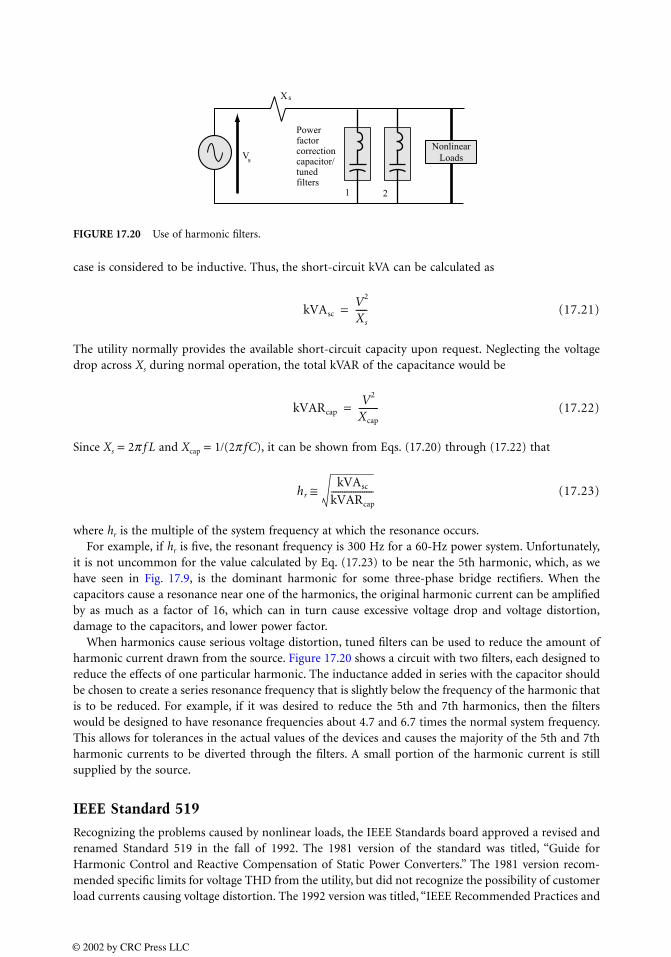
case is considered to be inductive. Thus, the short-circuit kVA can be calculated as
(17.21)
The utility normally provides the available short-circuit capacity upon request. Neglecting the voltagedrop across Xs during normal operation, the total kVAR of the capacitance would be
(17.22)
Since Xs = 2π f L and Xcap = 1/(2π fC), it can be shown from Eqs. (17.20) through (17.22) that
(17.23)
where hr is the multiple of the system frequency at which the resonance occurs. For example, if hr is five, the resonant frequency is 300 Hz for a 60-Hz power system. Unfortunately,
it is not uncommon for the value calculated by Eq. (17.23) to be near the 5th harmonic, which, as wehave seen in Fig. 17.9, is the dominant harmonic for some three-phase bridge rectifiers. When thecapacitors cause a resonance near one of the harmonics, the original harmonic current can be amplifiedby as much as a factor of 16, which can in turn cause excessive voltage drop and voltage distortion,damage to the capacitors, and lower power factor.
When harmonics cause serious voltage distortion, tuned filters can be used to reduce the amount ofharmonic current drawn from the source. Figure 17.20 shows a circuit with two filters, each designed toreduce the effects of one particular harmonic. The inductance added in series with the capacitor shouldbe chosen to create a series resonance frequency that is slightly below the frequency of the harmonic thatis to be reduced. For example, if it was desired to reduce the 5th and 7th harmonics, then the filterswould be designed to have resonance frequencies about 4.7 and 6.7 times the normal system frequency.This allows for tolerances in the actual values of the devices and causes the majority of the 5th and 7thharmonic currents to be diverted through the filters. A small portion of the harmonic current is stillsupplied by the source.
IEEE Standard 519
Recognizing the problems caused by nonlinear loads, the IEEE Standards board approved a revised andrenamed Standard 519 in the fall of 1992. The 1981 version of the standard was titled, “Guide forHarmonic Control and Reactive Compensation of Static Power Converters.” The 1981 version recom-mended specific limits for voltage THD from the utility, but did not recognize the possibility of customerload currents causing voltage distortion. The 1992 version was titled, “IEEE Recommended Practices and
FIGURE 17.20 Use of harmonic filters.
LoadsNonlinear
Powerfactorcorrectioncapacitor/tunedfilters
1 2
X s
Vs
kVAscV2
Xs
-----=
kVARcapV2
Xcap
---------=
hr
kVAsc
kVARcap
-------------------≅
© 2002 by CRC Press LLC

Requirements for Harmonic Control in Electrical Power Systems.” The new version places the responsi-bility for ensuring power quality on both the utility and the customer.
As indicated by the title, IEEE Standard 519 is a “recommended practice,” which means it is not a lawor rule for all utility–customer interfaces, but it may be used as a design guideline for new installations.Utilities may also include the requirements from Standard 519 in service agreements with their customers,which could result in financial penalties for customers that do not comply. The standard makes thecustomer responsible for limiting the harmonic currents injected into the power system and the utilityresponsible for avoiding unacceptable voltage distortion.
IEEE Standard 519 defines harmonic current limits (shown in Table 17.1) for individual customers atthe point of common coupling (PCC). Because voltage distortion is caused by the amount of harmoniccurrents in the system, larger customers are capable of causing more voltage distortion than smaller ones.Recognizing this, the standard allows a higher current THD for smaller customers’ loads. The short-circuit ratio (SCR) is used to differentiate customer size.
When the load of Fig. 17.19 was shorted, the only impedance limiting the current was the systemimpedance. That current is called the available short-circuit current, and is generally high since the systemimpedance is much lower than the load impedance. SCR is defined as the “average maximum demand(load) current” for the facility divided by the available short-circuit current. The maximum load currentdrawn by a large customer would be a higher fraction of the available short-circuit current, so the largecustomer’s SCR would be lower. The lower the SCR, the more stringent are the IEEE 519 limitations onharmonic currents.
IEEE Standard 519 also provides limits for specific ranges of frequencies, as shown in Table 17.1.Higher-order harmonics are constrained to have lower amplitudes for two reasons. First, higher-orderharmonics cause greater voltage distortion than lower-order harmonics, even if they have the sameamplitude, because the system inductive reactance is proportional to frequency. Second, interference withtelecommunication equipment is more severe for higher-frequency harmonics. Note that Table 17.1applies only to odd harmonics; even harmonics are limited to 25% of the values for the ranges theywould occupy in Table 17.1.
The utility is required by Standard 519 to maintain acceptable levels of voltage distortion. Below 69 kV,individual harmonic components in the voltage should not exceed 3% of the fundamental, and the voltageTHD must be less than 5%. Higher voltages have even lower limits, but those apply primarily to utilityinterconnections.
References
Bingham, R. P., Planning and performing a power quality survey, Power Qual. Assurance, 9(3), May/June1998.
Dugan, R. C., M. F. McGranaghan, and H. W. Beaty, Electrical Power Systems Quality, McGraw-Hill,New York, 1996.
Grady, W. M., Harmonics and how they relate to power quality, in Proceedings of the EPRI Power Qualityand Opportunities Conference (PQA ’93), San Diego, CA, November 1993.
Guth, B., Pay me now or pay me later—power monitors and conditioners provide valuable insurancewhen it comes time to install modern and expensive electrical systems and equipment, Consulting-Specifying Eng., Vol. 3, September 1997.
TABLE 17.1 Harmonics Allowed by IEEE Standard 519
SCR h < 11 11–15 17–21 23–33 h > 33 % THD
<20 4.0 2.0 1.5 0.6 0.3 5.020–50 7.0 3.5 2.5 1.0 0.5 8.050–100 10.0 4.5 4.0 1.5 0.7 12.0100–1000 12.0 5.5 5.0 2.0 1.0 15.0>1000 15.0 7.0 6.0 2.5 1.4 20.0
© 2002 by CRC Press LLC

Handbook of Power Signatures, 1993, Basic Measuring Instruments, Santa Clara, CA.IEEE Standard 519-1992, IEEE Recommended Practices and Requirements for Harmonic Control in
Electrical Power Systems.IEEE Standard 1100-1992, IEEE Recommended Practice for Powering and Grounding of Sensitive Elec-
tronic Equipment.IEEE Standard 1159-1995, IEEE Recommended Practice for Monitoring Electric Power Quality.Waller, M., Managing the Computer Power Environment—A Guide to Clean Power for Electronic Systems,
1992, Prompt Publications, Indianapolis, IN.
17.3 Passive Harmonic Filters
Badrul H. Chowdhury
Currently in the United States, only 15 to 20% of the utility distribution loading consists of nonlinearloads. Loads, such as AC and DC adjustable speed drives (ASD), power rectifiers and inverters, arc furnaces,and discharge lighting (metal halide, fluorescent, etc.), and even saturated transformers, can be considerednonlinear devices. It is projected over the next 10 years that such nonlinear loads will comprise approx-imately 70 to 85% of the loading on utility distribution systems in the United States. These loads maygenerate enough harmonics to cause distorted current and voltage waveshapes.
The deleterious effects of harmonics are many. A significant impact is equipment overheating becauseof the presence of harmonics in addition to the fundamental. Harmonics can also create resonanceconditions with power factor correction capacitors, resulting in higher than normal currents and voltages.This can lead to improper operation of protective devices, such as relays and fuses.
Harmonic frequency currents can cause additional rotating fields in AC motors. Depending on thefrequency, the motor will rotate in the opposite direction (countertorque). In particular, the 5th harmonic,which is the most prevalent harmonic in three-phase power systems, is a negative sequence harmoniccausing the motor to have a backward rotation, thus shortening the service life.
A typical current wave, as drawn by a three-phase AC motor drive, may look like the waveshape shownin Fig. 17.21. A Fourier analysis of the current would reveal the nature of the harmonics present. Three-phase ASDs generate primarily the 5th and 7th current harmonics and a lesser amount of 11th, 13th, andhigher orders. The triplen harmonics (3rd, 9th, 15th, i.e., odd multiples of three) are conspicuously missing,as is usually the case in six-pulse converters, giving them an added advantage over single-phase converters.However, the triplen harmonics are additive in the neutral and can cause dangerous overheating.
In general, the characteristic harmonics generated by a converter is given by
(17.24)
FIGURE 17.21 Typical current waveform of a three-phase adjustable-speed drive.
h pn 1p 6, 12, 18, …=n 1, 2, …=
±=
© 2002 by CRC Press LLC

where h is the order of harmonics, n is any integer, and p is the number of pulses generated in each cycle(six for a three-phase converter).
To understand the impact of harmonics and to design remedies, one must quantify the amount ofharmonics present. This is done by combining all of the harmonic frequency components (voltage orcurrent) with the fundamental component (voltage or current) to form the total harmonic distortion,or THD. A commonly accepted definition of THD is as follows:
(17.25)
where I1 is the fundamental component of the current, I2 is the second harmonic, I3 the third harmonic,and so on. A similar equation can be written for voltage distortion.
Any THD values over 5% are significant enough for concern. Harmonic current distortion greaterthan 5% will contribute to the additional heating of a power transformer, so it must be derated forharmonics. It is not uncommon for THD levels in industrial plants to reach 25%. Normally, THD levelsin office settings will be lower than in industrial plants, but office equipment is much more susceptibleto variations in power quality. Odd-number harmonics (3rd, 5th, 7th, etc.) are of the greatest concernin the electrical distribution system. Even-number harmonics are usually mitigated because the harmonicsswing equally in both the positive and negative direction. Pesky harmonics can be mitigated by the useof passive and active filters. Passive filters, consisting of tuned series L-C circuits, are the most popular.However, they require careful application, and may produce unwanted side effects, particularly in thepresence of power factor correction capacitors.
The active filter concept uses power electronics to produce harmonic components that cancel theharmonic components from the nonlinear loads so that the current supplied from the source is sinusoidal.These filters are costly and relatively new.
Passive harmonic filters are constructed from passive elements (resistors, inductors, and capacitors)and thus the name. These filters are highly suited for use in three-phase, four-wire electrical powerdistribution systems. They should be applied as close as possible to the offending loads, preferably at thefarthest three- to single-phase point of distribution. This will ensure maximum protection for theupstream system. Harmonics can be substantially reduced to as low as 30% by use of passive filters.
Passive filters can be categorized as parallel filters and series filters. A parallel filter is characterized asa series resonant and trap-type exhibiting a low impedance at its tuned frequency. Deployed close to thesource of distortion, this filter keeps the harmonic currents out of the supply system. It also providessome smoothing of the load voltage. This is the most common type of filter.
The series filter is characterized as a parallel resonant and blocking type with high impedance at itstuned frequency. It is not very common because the load voltage can be distorted.
Series Passive Filter
This configuration is popular for single-phase applications for the purpose of minimizing the 3rdharmonic. Other specific tuned frequencies can also be filtered. Figure 17.22 shows the basic diagram ofa series passive filter.
The advantages of a series filter are that it:
• Provides high impedance to tuned frequency;
• Does not introduce any system resonance;
• Does not import harmonics from other sources;
• Improves displacement power factor and true power factor.
THDI
I22 I3
2 I42 …+ + +
I1
----------------------------------------- 100%×Ih
2
h =2
∞
∑I1
--------------- 100%×= =
© 2002 by CRC Press LLC

Some disadvantages are that it:
• Must handle the rated full load current;
• Is only minimally effective other than tuned harmonic frequencies;
• Can supply nonlinear loads only.
Shunt Passive Filter
The shunt passive filter is also capable of filtering specific tuned harmonic frequencies such as, 5th, 7th,11th, etc. Figure 17.23 shows a commonly used diagram of a shunt filter. The advantages of a parallelfilter are that it:
• Provides low impedance to tuned frequency;
• Supplies specific harmonic component to load rather than from AC source;
• Is only required to carry harmonic current and not the full load current;
• Improves displacement power factor and true power factor.
Some disadvantages are that:
• It only filters a single (tuned) harmonic frequency;
• It can create system resonance;
• It can import harmonics form other nonlinear loads;
• Multiple filters are required to satisfy typical desired harmonic limits.
Series Passive AC Input Reactor
The basic configuration is shown in Fig. 17.24. This type filters all harmonic frequencies, by varyingamounts. The advantages of a series reactor are:
• Low cost;
• Higher true power factor;
• Small size;
FIGURE 17.22 A series passive filter.
FIGURE 17.23 A shunt passive filter.
C
Input Source
L
Output Load
C
LInput
Source Output Load
© 2002 by CRC Press LLC
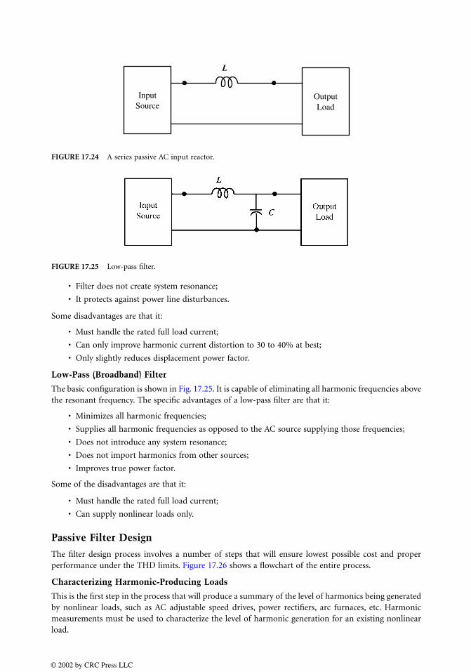
• Filter does not create system resonance;
• It protects against power line disturbances.
Some disadvantages are that it:
• Must handle the rated full load current;
• Can only improve harmonic current distortion to 30 to 40% at best;
• Only slightly reduces displacement power factor.
Low-Pass (Broadband) Filter
The basic configuration is shown in Fig. 17.25. It is capable of eliminating all harmonic frequencies abovethe resonant frequency. The specific advantages of a low-pass filter are that it:
• Minimizes all harmonic frequencies;
• Supplies all harmonic frequencies as opposed to the AC source supplying those frequencies;
• Does not introduce any system resonance;
• Does not import harmonics from other sources;
• Improves true power factor.
Some of the disadvantages are that it:
• Must handle the rated full load current;
• Can supply nonlinear loads only.
Passive Filter Design
The filter design process involves a number of steps that will ensure lowest possible cost and properperformance under the THD limits. Figure 17.26 shows a flowchart of the entire process.
Characterizing Harmonic-Producing Loads
This is the first step in the process that will produce a summary of the level of harmonics being generatedby nonlinear loads, such as AC adjustable speed drives, power rectifiers, arc furnaces, etc. Harmonicmeasurements must be used to characterize the level of harmonic generation for an existing nonlinearload.
FIGURE 17.24 A series passive AC input reactor.
FIGURE 17.25 Low-pass filter.
L
InputSource
OutputLoad
© 2002 by CRC Press LLC
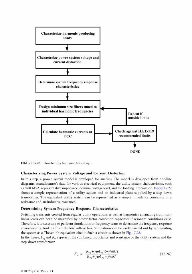
Characterizing Power System Voltage and Current Distortion
In this step, a power system model is developed for analysis. The model is developed from one-linediagrams, manufacturer’s data for various electrical equipment, the utility system characteristics, suchas fault MVA, representative impedance, nominal voltage level, and the loading information. Figure 17.27shows a sample representation of a utility system and an industrial plant supplied by a step-downtransformer. The equivalent utility system can be represented as a simple impedance consisting of aresistance and an inductive reactance.
Determining System Frequency Response Characteristics
Switching transients created from regular utility operations as well as harmonics emanating from non-linear loads can both be magnified by power factor correction capacitors if resonant conditions exist.Therefore, it is necessary to perform simulations or frequency scans to determine the frequency responsecharacteristics, looking from the low voltage bus. Simulations can be easily carried out by representingthe system as a Thevenin’s equivalent circuit. Such a circuit is shown in Fig. 17.28.In the figure, Leq and Req represent the combined inductance and resistance of the utility system and thestep-down transformer.
(17.26)
FIGURE 17.26 Flowchart for harmonic filter design.
Repeat if outside limits
DONE
Determine system frequency responsecharacteristics
Characterize power system voltage andcurrent distortion
Characterize harmonic producingloads
Design minimum size filters tuned toindividual harmonic frequencies
Calculate harmonic currents at PCC
Check against IEEE-519recommended limits
Zin
Req jwLeq+( ) −j/wC( )Req jwLeq j/wC–+
----------------------------------------------------=
© 2002 by CRC Press LLC
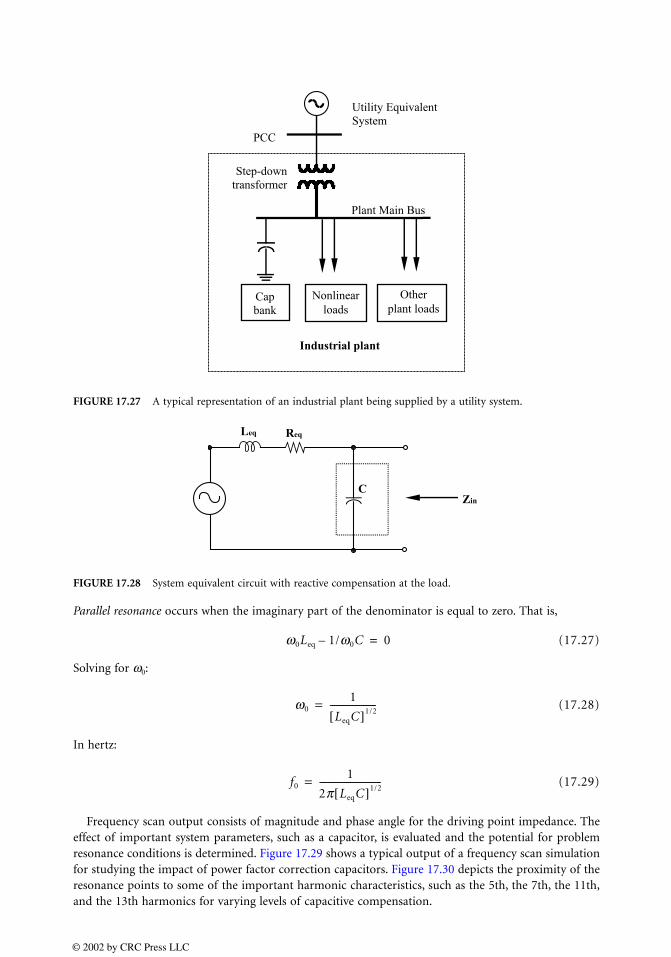
Parallel resonance occurs when the imaginary part of the denominator is equal to zero. That is,
(17.27)
Solving for ω0:
(17.28)
In hertz:
(17.29)
Frequency scan output consists of magnitude and phase angle for the driving point impedance. Theeffect of important system parameters, such as a capacitor, is evaluated and the potential for problemresonance conditions is determined. Figure 17.29 shows a typical output of a frequency scan simulationfor studying the impact of power factor correction capacitors. Figure 17.30 depicts the proximity of theresonance points to some of the important harmonic characteristics, such as the 5th, the 7th, the 11th,and the 13th harmonics for varying levels of capacitive compensation.
FIGURE 17.27 A typical representation of an industrial plant being supplied by a utility system.
FIGURE 17.28 System equivalent circuit with reactive compensation at the load.
Step-down transformer
Other plant loads
Nonlinear loads
Cap bank
Utility Equivalent System
PCC
Industrial plant
Plant Main Bus
Leq
C
Req
Zin
w0Leq 1/w0C– 0=
w01
LeqC[ ]1/2---------------------=
f01
2p LeqC[ ]1/2----------------------------=
© 2002 by CRC Press LLC
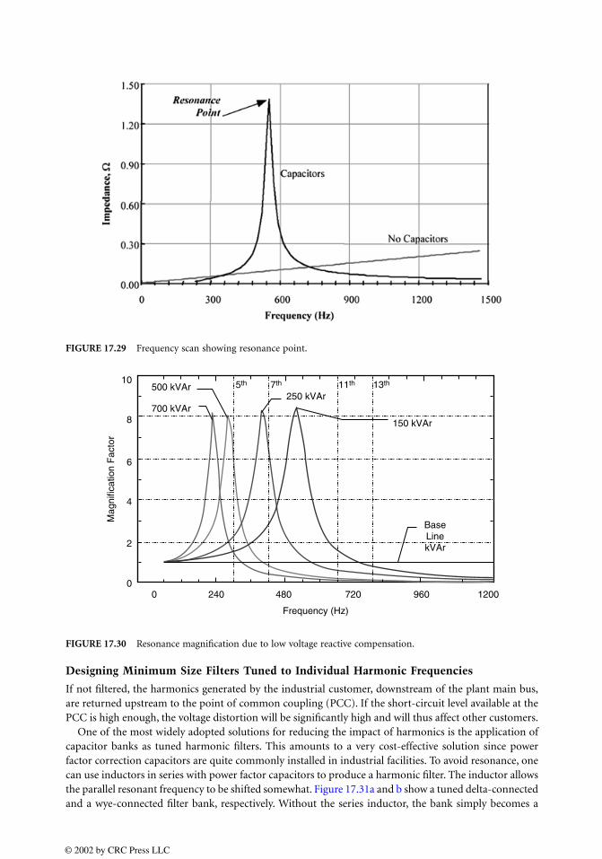
Designing Minimum Size Filters Tuned to Individual Harmonic Frequencies
If not filtered, the harmonics generated by the industrial customer, downstream of the plant main bus,are returned upstream to the point of common coupling (PCC). If the short-circuit level available at thePCC is high enough, the voltage distortion will be significantly high and will thus affect other customers.
One of the most widely adopted solutions for reducing the impact of harmonics is the application ofcapacitor banks as tuned harmonic filters. This amounts to a very cost-effective solution since powerfactor correction capacitors are quite commonly installed in industrial facilities. To avoid resonance, onecan use inductors in series with power factor capacitors to produce a harmonic filter. The inductor allowsthe parallel resonant frequency to be shifted somewhat. Figure 17.31a and b show a tuned delta-connectedand a wye-connected filter bank, respectively. Without the series inductor, the bank simply becomes a
FIGURE 17.29 Frequency scan showing resonance point.
FIGURE 17.30 Resonance magnification due to low voltage reactive compensation.
BaseLinekVAr
150 kVAr
250 kVAr500 kVAr
700 kVAr
13th11th7th5th
00
2
4
6
8
10
Mag
nific
atio
n F
acto
r
240 480 720
Frequency (Hz)
960 1200
© 2002 by CRC Press LLC
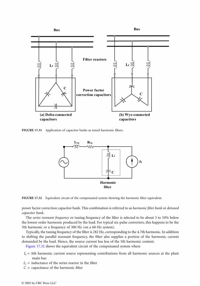
power factor correction capacitor bank. This combination is referred to as harmonic filter bank or detunedcapacitor bank.
The series resonant frequency or tuning frequency of the filter is selected to be about 3 to 10% belowthe lowest-order harmonic produced by the load. For typical six-pulse converters, this happens to be the5th harmonic or a frequency of 300 Hz (on a 60-Hz system).
Typically, the tuning frequency of the filter is 282 Hz, corresponding to the 4.7th harmonic. In additionto shifting the parallel resonant frequency, the filter also supplies a portion of the harmonic currentdemanded by the load. Hence, the source current has less of the 5th harmonic content.
Figure 17.32 shows the equivalent circuit of the compensated system where
Ih = hth harmonic current source representing contributions from all harmonic sources at the plantmain bus
Lf = inductance of the series reactor in the filterC = capacitance of the harmonic filter
FIGURE 17.31 Application of capacitor banks as tuned harmonic filters.
FIGURE 17.32 Equivalent circuit of the compensated system showing the harmonic filter equivalent.
Bus
Filter reactors
Bus
Lf
C
Lf
C
(a) Delta-connectedcapacitors
Power factorcorrection capacitors
(b) Wye-connectedcapacitors
C
Leq Req
Harmonicfilter
Ih
Lf
© 2002 by CRC Press LLC

Depending on the severity of the individual harmonic level, harmonic filters should be tuned to aharmonic that causes the resonance condition. Some useful equations are given below.
Series resonant frequency of the filter element is
(17.30)
where Lf = inductance of the tuning inductor and C = capacitance of the capacitor bank.Solving for Lf :
(17.31)
Since
(17.32)
where
(17.33)
(17.34)
Thus, the driving point impedance, as seen in Fig. 17.32, is
(17.35)
Parallel resonance occurs when the imaginary part of the denominator is equal to zero. That is,
(17.36)
Solving for ω0:
(17.37)
In hertz:
(17.38)
If the design is correct, then the frequency given by Eq. (17.38) should be farther away from the resonancepoint.
f01
2p Lf C[ ]1/2--------------------------=
Lf1
C 2pf0
[ ]2---------------------=
C1
2pfsysXcap
---------------------- 1wsysXcap
------------------= =
Xcap
KVcap2
MVAcap
-------------------=
Lf
fsysXcap
2p f0( )2------------------
fsyskVcap2
2p f0( )2MVAcap
-------------------------------------= =
Zin
Req jwLeq+( ) jwLf j/wC–( )Req jwLeq jwLf j/wC–+ +
-------------------------------------------------------------------=
w0Leq w0Lf 1/w0C–+ 0=
w01
Leq Lf+( )C[ ]1/2------------------------------------=
f01
2p Leq Lf+( )C[ ]1/2-------------------------------------------=
© 2002 by CRC Press LLC

Calculating Harmonic Currents at PCC
To carry out simulations to estimate actual harmonic distortion levels, one needs to represent eachharmonic-generating device, the system parameters, and the tuned filter characteristics. The output forthese simulations consists of individual harmonic levels, bus voltage distortion and current distortionlevels, and rms voltage and current levels. Harmonic levels are calculated at the PCC where the consumer’sload connects to other loads in the power system.
Checking against IEEE-519 Recommended Limits
Current and voltage distortion levels as determined through simulations are compared with recom-mended limits outlined in IEEE Standard 519-1992. This standard is explained in the Appendix to thissection. If harmonic voltage distortion levels are still not within acceptable limits, it is easy to changecapacitor sizes and/or locations, or the size of the series reactor. These changes affect the frequencyresponse characteristics of the industrial facility such that proximity to resonance points can be altered.
Further Information
Cameron, M., Trends in power factor correction with harmonic filtering, IEEE Trans. Ind. Appl., 29,60–65, 1993.
Dugan, R. C., McGranaghan, M. F., and Beaty, H. W., Electrical Power Systems Quality, McGraw-Hill,New York, 1996.
Fujita, H. and Akagi, H., A practical approach to harmonic compensation in power systems—seriesconnection of passive and active filters, IEEE Trans. Ind. Appl., 27(6), 1020–1025, 1991.
Grady, W. W., Samotyj, M. J., and Noyola, A. H., Survey of active power line conditioning methodologies,IEEE Trans. Power Delivery, 5(3), 1536–1542, 1990.
Grebe, T. E., Application of distribution system capacitor banks and their impact on power quality, IEEETrans. Ind. Appl., 32(3), 714–719, 1996.
IEEE Harmonics Working Group, IEEE Recommended Practices and Requirements for Harmonic Con-trol in Electrical Power Systems, IEEE STD 519-1992, New York: IEEE, 1993.
IEEE P519A Task Force of the PES Harmonics Working Group, Guide for Applying Harmonic Limits onPower Systems, IEEE, New York, 1996.
Lemieux, G., Power system harmonic resonance—a documented case, IEEE Trans. Ind. Appl., 26(3),483–485, 1990.
Lowenstein, M. Z., Improving power factor in the presence of harmonics using low-voltage tuned filters,IEEE Trans. Ind. Appl., 29, 528–535, 1993.
Makram, E. B. et al., Harmonic filter design using actual recorded data, IEEE Trans. Ind. Appl., 29(6),1176–1183, 1993.
Peng, F. Z., Akagi, H., and Nabae, A., Compensation characteristics of combined system of shunt passiveand series active filters, in IEEE/IAS Annual Meet. Conf. Record, 1989, 959–966.
Phipps, J. K., A transfer function approach to harmonic filter design, Ind. Appl. Mag., 3(2), 68–82, 1997.
Appendix—IEEE Recommended Practices and Requirements for Harmonic Control in Electric Power Systems
IEEE 519-1992 recommends limits on harmonic distortion according to two distinct criteria:
1. There is a limitation on the amount of harmonic current that a consumer can inject into a utilitynetwork.
2. A limitation is placed on the level of harmonic voltage that a utility can supply to a consumer.
SCRShort-circuit MVA
Load MW---------------------------------------------
ISC
IL
------= =
© 2002 by CRC Press LLC

IEEE 519 is limited to being a collection of Recommended Practices that serve as a guide to both suppliersand consumers of electrical energy with regard to excessive harmonic current injection or excessive voltagedistortion. All of the current distortion values are given in terms relative to the maximum demand loadcurrent. The total distortion is in terms of total demand distortion (TDD) instead of the more commonTHD term. ISC = maximum short circuit current at PCC; IL = maximum demand load current (fundamentalfrequency) at point of common coupling; TDD = Total demand distortion in % of max demand andgiven by
17.4 Active Filters for Power Conditioning
Hirofumi Akagi
Much research has been performed on active filters for power conditioning and their practical applicationssince their basic principles of compensation were proposed around 1970 [Bird et al., 1969; Gyugyi andStrycula, 1976; Kawahira et al., 1983]. In particular, recent remarkable progress in the capacity and switch-ing speed of power semiconductor devices such as insulated-gate bipolar transistors (IGBTs) has spurredinterest in active filters for power conditioning. In addition, state-of-the-art power electronics technologyhas enabled active filters to be put into practical use. More than one thousand sets of active filtersconsisting of voltage-fed pulse width modulation (PWM) inverters using IGBTs or gate turn-off (GTO)thyristors are operating successfully in Japan.
Active filters for power conditioning provide the following functions:
• Reactive-power compensation,
• Harmonic compensation, harmonic isolation, harmonic damping, and harmonic termination,
• Negative sequence current/voltage compensation,
• Voltage regulation.
The term active filters is also used in the field of signal processing. In order to distinguish active filtersin power processing from active filters in signal processing, the term active power filters often appears inmany technical papers or literature. However, the author prefers active filters for power conditioning toactive power filters, because the term active power filters is misleading to either active filters for poweror filters for active power. Therefore, this section takes the term active filters for power conditioning orsimply uses the term active filters as long as no confusion occurs.
Harmonic-Producing Loads
Identified Loads and Unidentified Loads
Nonlinear loads drawing nonsinusoidal currents from utilities are classified into identified and uniden-tified loads. High-power diode/thyristor rectifiers, cycloconverters, and arc furnaces are typically char-acterized as identified harmonic-producing loads because utilities identify the individual nonlinear loadsinstalled by high-power consumers on power distribution systems in many cases. The utilities determinethe point of common coupling with high-power consumers who install their own harmonic-producingloads on power distribution systems, and also can determine the amount of harmonic current injectedfrom an individual consumer.
A “single” low-power diode rectifier produces a negligible amount of harmonic current. However,multiple low-power diode rectifiers can inject a large amount of harmonics into power distribution
TDD
Ih2
h=2
∞
∑IL
--------------- 100%×=
© 2002 by CRC Press LLC
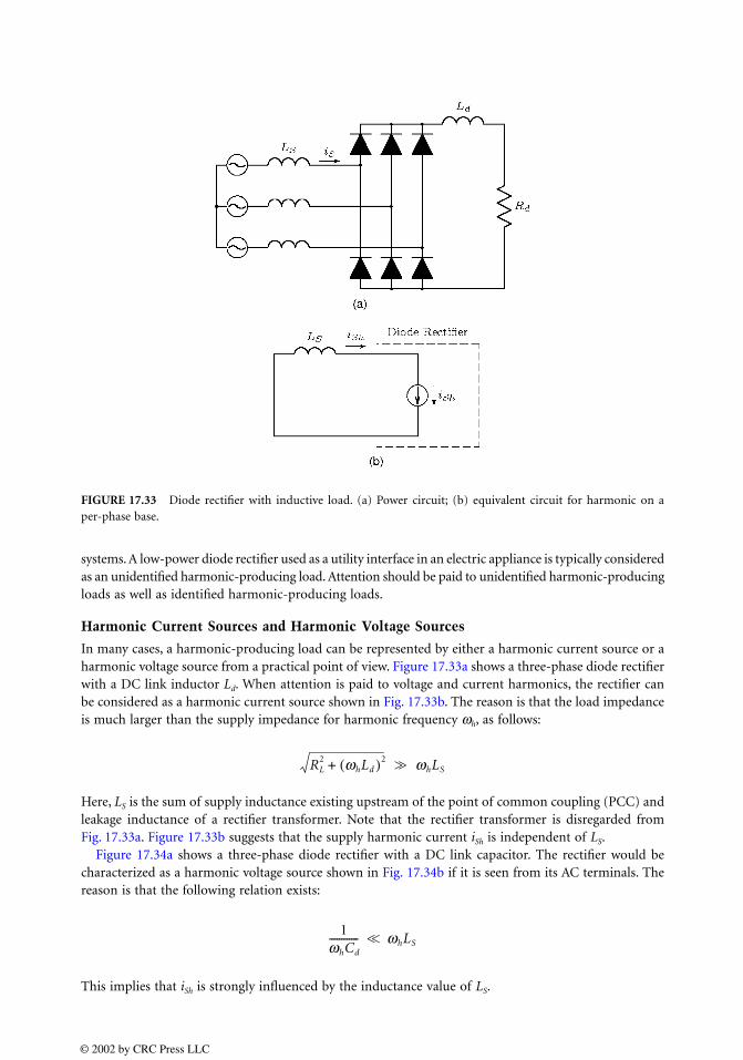
systems. A low-power diode rectifier used as a utility interface in an electric appliance is typically consideredas an unidentified harmonic-producing load. Attention should be paid to unidentified harmonic-producingloads as well as identified harmonic-producing loads.
Harmonic Current Sources and Harmonic Voltage Sources
In many cases, a harmonic-producing load can be represented by either a harmonic current source or aharmonic voltage source from a practical point of view. Figure 17.33a shows a three-phase diode rectifierwith a DC link inductor Ld. When attention is paid to voltage and current harmonics, the rectifier canbe considered as a harmonic current source shown in Fig. 17.33b. The reason is that the load impedanceis much larger than the supply impedance for harmonic frequency ωh, as follows:
Here, LS is the sum of supply inductance existing upstream of the point of common coupling (PCC) andleakage inductance of a rectifier transformer. Note that the rectifier transformer is disregarded fromFig. 17.33a. Figure 17.33b suggests that the supply harmonic current iSh is independent of LS.
Figure 17.34a shows a three-phase diode rectifier with a DC link capacitor. The rectifier would becharacterized as a harmonic voltage source shown in Fig. 17.34b if it is seen from its AC terminals. Thereason is that the following relation exists:
This implies that iSh is strongly influenced by the inductance value of LS.
FIGURE 17.33 Diode rectifier with inductive load. (a) Power circuit; (b) equivalent circuit for harmonic on aper-phase base.
RL2 whLd( )2+ >> whLS
1whCd
------------ << whLS
© 2002 by CRC Press LLC
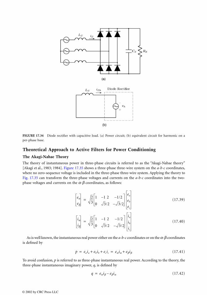
Theoretical Approach to Active Filters for Power Conditioning
The Akagi-Nabae Theory
The theory of instantaneous power in three-phase circuits is referred to as the “Akagi-Nabae theory”[Akagi et al., 1983; 1984]. Figure 17.35 shows a three-phase three-wire system on the a-b-c coordinates,where no zero-sequence voltage is included in the three-phase three-wire system. Applying the theory toFig. 17.35 can transform the three-phase voltages and currents on the a-b-c coordinates into the two-phase voltages and currents on the α-β coordinates, as follows:
(17.39)
(17.40)
As is well known, the instantaneous real power either on the a-b-c coordinates or on the α-β coordinatesis defined by
(17.41)
To avoid confusion, p is referred to as three-phase instantaneous real power. According to the theory, thethree-phase instantaneous imaginary power, q, is defined by
(17.42)
FIGURE 17.34 Diode rectifier with capacitive load. (a) Power circuit; (b) equivalent circuit for harmonic on aper-phase base.
ea
eb
23--
1 1 2– 1/2–
0 3/2 3/2–
ea
eb
ec
=
ia
ib
23--
1 1 2– 1/2–
0 3/2 3/2–
ia
ib
ic
=
p eaia ebib ecic+ + eaia ebib+= =
q eaib ebia–=
© 2002 by CRC Press LLC
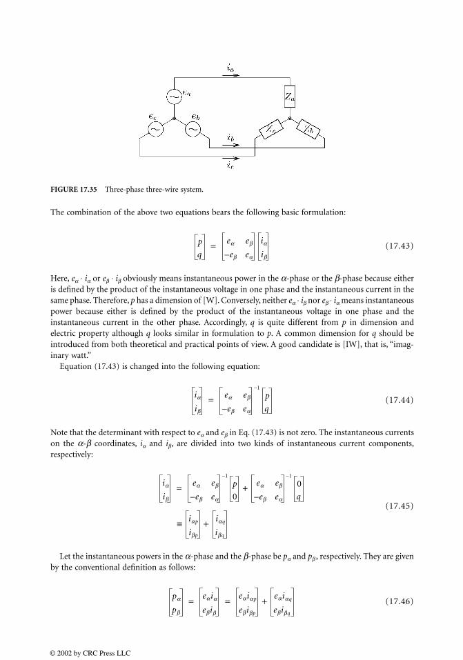
The combination of the above two equations bears the following basic formulation:
(17.43)
Here, eα ⋅ iα or eβ ⋅ iβ obviously means instantaneous power in the α-phase or the β-phase because eitheris defined by the product of the instantaneous voltage in one phase and the instantaneous current in thesame phase. Therefore, p has a dimension of [W]. Conversely, neither eα ⋅ iβ nor eβ ⋅ iα means instantaneouspower because either is defined by the product of the instantaneous voltage in one phase and theinstantaneous current in the other phase. Accordingly, q is quite different from p in dimension andelectric property although q looks similar in formulation to p. A common dimension for q should beintroduced from both theoretical and practical points of view. A good candidate is [IW], that is, “imag-inary watt.”
Equation (17.43) is changed into the following equation:
(17.44)
Note that the determinant with respect to eα and eβ in Eq. (17.43) is not zero. The instantaneous currentson the α-β coordinates, iα and iβ, are divided into two kinds of instantaneous current components,respectively:
(17.45)
Let the instantaneous powers in the α-phase and the β-phase be pα and pβ , respectively. They are givenby the conventional definition as follows:
(17.46)
FIGURE 17.35 Three-phase three-wire system.
p
q
ea eb
e– b ea
ia
ib
=
ia
ib
ea eb
e– b ea
1–
p
q=
ia
ib
ea eb
e– b ea
1–
p
0
ea eb
e– b ea
1–
0
q+=
iap
ibp
iaq
ibq
+≡
pa
pb
eaia
ebib
eaiap
ebibp
eaiaq
ebibq
+= =
© 2002 by CRC Press LLC
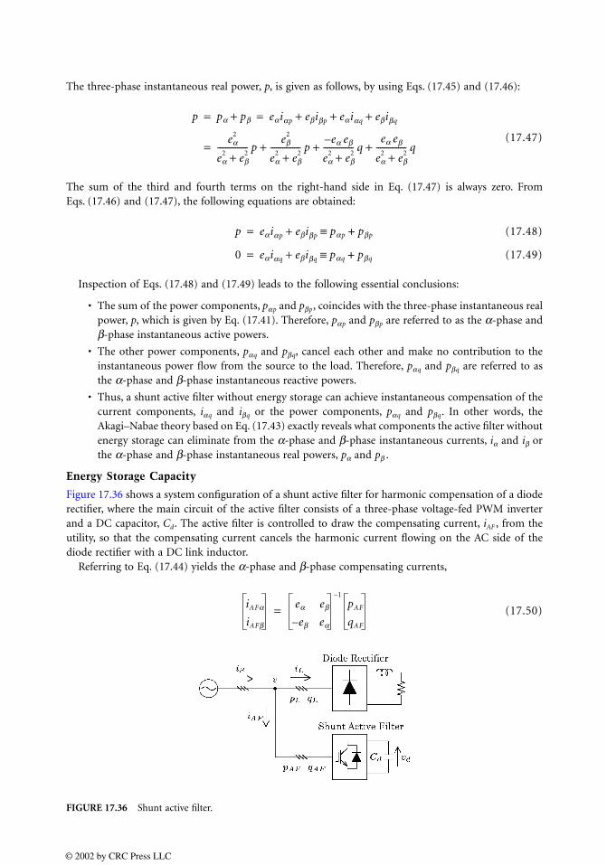
The three-phase instantaneous real power, p, is given as follows, by using Eqs. (17.45) and (17.46):
(17.47)
The sum of the third and fourth terms on the right-hand side in Eq. (17.47) is always zero. FromEqs. (17.46) and (17.47), the following equations are obtained:
(17.48)
(17.49)
Inspection of Eqs. (17.48) and (17.49) leads to the following essential conclusions:
• The sum of the power components, pαp and pβp, coincides with the three-phase instantaneous realpower, p, which is given by Eq. (17.41). Therefore, pαp and pβp are referred to as the α-phase andβ-phase instantaneous active powers.
• The other power components, pαq and pβq, cancel each other and make no contribution to theinstantaneous power flow from the source to the load. Therefore, pαq and pβq are referred to asthe α-phase and β-phase instantaneous reactive powers.
• Thus, a shunt active filter without energy storage can achieve instantaneous compensation of thecurrent components, iαq and iβq or the power components, pαq and pβq. In other words, theAkagi–Nabae theory based on Eq. (17.43) exactly reveals what components the active filter withoutenergy storage can eliminate from the α-phase and β-phase instantaneous currents, iα and iβ orthe α-phase and β-phase instantaneous real powers, pα and pβ .
Energy Storage Capacity
Figure 17.36 shows a system configuration of a shunt active filter for harmonic compensation of a dioderectifier, where the main circuit of the active filter consists of a three-phase voltage-fed PWM inverterand a DC capacitor, Cd. The active filter is controlled to draw the compensating current, iAF , from theutility, so that the compensating current cancels the harmonic current flowing on the AC side of thediode rectifier with a DC link inductor.
Referring to Eq. (17.44) yields the α-phase and β-phase compensating currents,
(17.50)
FIGURE 17.36 Shunt active filter.
p pa pb+ eaiap ebibp eaiaq ebibq+ + += =
ea2
ea2 eb
2+--------------- p
eb2
ea2 eb
2+--------------- p
e– a eb
ea2 eb
2+--------------- q
ea eb
ea2 eb
2+--------------- q+ + +=
p eaiap ebibp+ pap pbp+≡=
0 eaiaq ebibq+ paq pbq+≡=
iAFa
iAFb
ea eb
e– b ea
1–
pAF
qAF
=
© 2002 by CRC Press LLC

Here, pAF and qAF are the three-phase instantaneous real and imaginary power on the AC side of theactive filter, and they are usually extracted from pL and qL. Note that pL and qL are the three-phaseinstantaneous real and imaginary power on the AC side of a harmonic-producing load. For instance,when the active filter compensates for the harmonic current produced by the load, the following rela-tionships exist:
(17.51)
Here, and are AC components of pL and qL, respectively. Note that the DC components of pL andqL correspond to the fundamental current present in iL and the AC components to the harmonic current.In general, two high-pass filters in the control circuit extract from pL and from qL.
The active filter draws pAF from the utility, and delivers it to the DC capacitor if no loss is dissipatedin the active filter. Thus, pAF induces voltage fluctuation of the DC capacitor. When the amplitude of pAF
is assumed to be constant, the lower the frequency of the AC component, the larger the voltage fluctuation[Akagi et al., 1984; 1986]. If the period of the AC component is one hour, the DC capacitor has to absorbor release electric energy given by integration of pAF with respect to time. Thus, the following relationshipexists between the instantaneous voltage across the DC capacitor, vd and pAF :
(17.52)
This implies that the active filter needs an extremely large-capacity DC capacitor to suppress the voltagefluctuation coming from achieving “harmonic” compensation of Hence, the active filter is no longera harmonic compensator, and thereby it should be referred to as a “DC capacitor-based energy storagesystem,” although it is impractical at present. In this case, the main purpose of the voltage-fed PWMinverter is to perform an interface between the utility and the bulky DC capacitor.
The active filter seems to “draw” qAF from the utility, as shown in Fig. 17.36. However, qAF makes nocontribution to energy transfer in the three-phase circuit. No energy storage, therefore, is required tothe active filter, independent of qAF , whenever pAF = 0.
Classification of Active Filters
Various types of active filters have been proposed in technical literature [Moran, 1989; Grady et al., 1990;Akagi, 1994; Akagi and Fujita, 1995; 1997; Aredes et al., 1998]. Classification of active filters is made fromdifferent points of view [Akagi, 1996]. Active filters are divided into AC and DC filters. Active DC filtershave been designed to compensate for current and/or voltage harmonics on the DC side of thyristorconverters for high-voltage DC transmission systems [Watanabe, 1990; Zhang et al., 1993] and on theDC link of a PWM rectifier/inverter for traction systems. Emphasis, however, is put on active AC filterin the following because the term “active filters” refers to active AC filters in most cases.
Classification by Objectives: Who Is Responsible for Installing Active Filters?
The objective of “who is responsible for installing active filters” classifies them into the following twogroups:
1. Active filters installed by individual consumers on their own premises in the vicinity of one ormore identified harmonic-producing loads.
2. Active filters being installed by electric power utilities in substations and/or on distribution feeders.
Individual consumers should pay attention to current harmonics produced by their own harmonic-producing loads, and thereby the active filters installed by the individual consumers are aimed at com-pensating for current harmonics.
pAF pL, qAF– qL˜–= =
pL qL
pL qL
12--Cdvd
2 t( ) 12--Cdvd
2 0( ) pAF td0
t
∫+=
pL.
© 2002 by CRC Press LLC

Utilities should concern themselves with voltage harmonics, and therefore active filters will be installedby utilities in the near future for the purpose of compensating for voltage harmonics and/or of achieving“harmonic damping” throughout power distribution systems or “harmonic termination” of a radialpower distribution feeder.
Classification by System Configuration
Shunt Active Filters and Series Active FiltersA stand-alone shunt active filter shown in Fig. 17.36 is one of the most fundamental system configurations.The active filter is controlled to draw a compensating current, iAF , from the utility, so that it cancelscurrent harmonics on the AC side of a general-purpose diode/thyristor rectifier [Akagi et al., 1990; Penget al., 1990; Bhattacharya et al., 1998] or a PWM rectifier for traction systems [Krah and Holtz, 1994].Generally, the shunt active filter is suitable for harmonic compensation of a current harmonic sourcesuch as diode/thyristor rectifier with a DC link inductor. The shunt active filter has the capability ofdamping harmonic resonance between an existing passive filter and the supply impedance.
Figure 17.37 shows a system configuration of a series active filter used alone. The series active filter isconnected in series with the utility through a matching transformer, so that it is suitable for harmoniccompensation of a voltage harmonic source such as a large-capacity diode rectifier with a DC linkcapacitor. The series active filter integrated into a diode rectifier with a DC common capacitor is discussedelsewhere. Table 17.2 shows comparisons between the shunt and series active filters. This concludes thatthe series active filter has a “dual” relationship in each item with the shunt active filter [Akagi, 1996;Peng, 1998].
Hybrid Active/Passive FiltersFigures 17.38 through 17.40 show three types of hybrid active/passive filters, the main purpose of whichis to reduce initial costs and to improve efficiency. The shunt passive filter consists of one or more tunedLC filters and/or a high-pass filter. Table 17.3 shows comparisons among the three hybrid filters in which
TABLE 17.2 Comparison of Shunt Active Filters and Series Active Filters
Shunt Active Filter Series Active Filter
System configuration Fig. 17.36 Fig. 17.37Power circuit of active filter Voltage-fed PWM inverter with
current minor loopVoltage-fed PWM inverter without current
minor loopActive filter acts as Current source: iAF Voltage source: vAF
Harmonic-producing load suitable
Diode/thyristor rectifiers with inductive loads, and cycloconverters
Large-capacity diode rectifiers with capacitive loads
Additional function Reactive power compensation AC voltage regulationPresent situation Commercial stage Laboratory stage
FIGURE 17.37 Series active filter.
© 2002 by CRC Press LLC
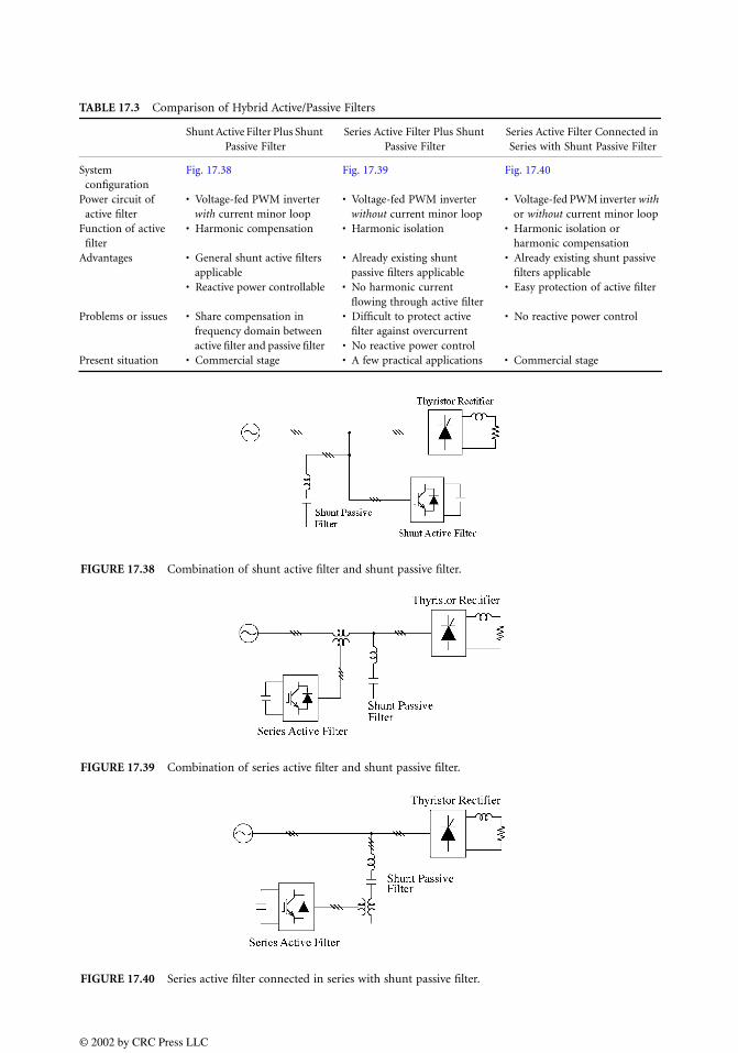
TABLE 17.3 Comparison of Hybrid Active/Passive Filters
Shunt Active Filter Plus Shunt Passive Filter
Series Active Filter Plus Shunt Passive Filter
Series Active Filter Connected in Series with Shunt Passive Filter
System configuration
Fig. 17.38 Fig. 17.39 Fig. 17.40
Power circuit of active filter
• Voltage-fed PWM inverter with current minor loop
• Voltage-fed PWM inverter without current minor loop
• Voltage-fed PWM inverter with or without current minor loop
Function of active filter
• Harmonic compensation • Harmonic isolation • Harmonic isolation or harmonic compensation
Advantages • General shunt active filters applicable
• Already existing shunt passive filters applicable
• Already existing shunt passive filters applicable
• Reactive power controllable • No harmonic current flowing through active filter
• Easy protection of active filter
Problems or issues • Share compensation in frequency domain between active filter and passive filter
• Difficult to protect active filter against overcurrent
• No reactive power control
• No reactive power control
Present situation • Commercial stage • A few practical applications • Commercial stage
FIGURE 17.38 Combination of shunt active filter and shunt passive filter.
FIGURE 17.39 Combination of series active filter and shunt passive filter.
FIGURE 17.40 Series active filter connected in series with shunt passive filter.
© 2002 by CRC Press LLC
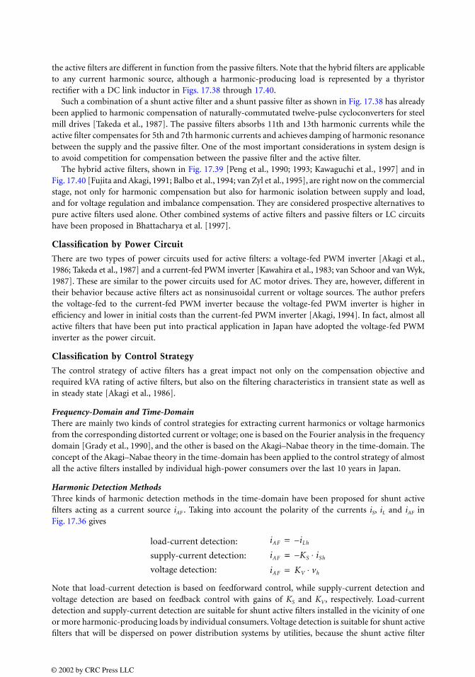
the active filters are different in function from the passive filters. Note that the hybrid filters are applicableto any current harmonic source, although a harmonic-producing load is represented by a thyristorrectifier with a DC link inductor in Figs. 17.38 through 17.40.
Such a combination of a shunt active filter and a shunt passive filter as shown in Fig. 17.38 has alreadybeen applied to harmonic compensation of naturally-commutated twelve-pulse cycloconverters for steelmill drives [Takeda et al., 1987]. The passive filters absorbs 11th and 13th harmonic currents while theactive filter compensates for 5th and 7th harmonic currents and achieves damping of harmonic resonancebetween the supply and the passive filter. One of the most important considerations in system design isto avoid competition for compensation between the passive filter and the active filter.
The hybrid active filters, shown in Fig. 17.39 [Peng et al., 1990; 1993; Kawaguchi et al., 1997] and inFig. 17.40 [Fujita and Akagi, 1991; Balbo et al., 1994; van Zyl et al., 1995], are right now on the commercialstage, not only for harmonic compensation but also for harmonic isolation between supply and load,and for voltage regulation and imbalance compensation. They are considered prospective alternatives topure active filters used alone. Other combined systems of active filters and passive filters or LC circuitshave been proposed in Bhattacharya et al. [1997].
Classification by Power Circuit
There are two types of power circuits used for active filters: a voltage-fed PWM inverter [Akagi et al.,1986; Takeda et al., 1987] and a current-fed PWM inverter [Kawahira et al., 1983; van Schoor and van Wyk,1987]. These are similar to the power circuits used for AC motor drives. They are, however, different intheir behavior because active filters act as nonsinusoidal current or voltage sources. The author prefersthe voltage-fed to the current-fed PWM inverter because the voltage-fed PWM inverter is higher inefficiency and lower in initial costs than the current-fed PWM inverter [Akagi, 1994]. In fact, almost allactive filters that have been put into practical application in Japan have adopted the voltage-fed PWMinverter as the power circuit.
Classification by Control Strategy
The control strategy of active filters has a great impact not only on the compensation objective andrequired kVA rating of active filters, but also on the filtering characteristics in transient state as well asin steady state [Akagi et al., 1986].
Frequency-Domain and Time-DomainThere are mainly two kinds of control strategies for extracting current harmonics or voltage harmonicsfrom the corresponding distorted current or voltage; one is based on the Fourier analysis in the frequencydomain [Grady et al., 1990], and the other is based on the Akagi–Nabae theory in the time-domain. Theconcept of the Akagi–Nabae theory in the time-domain has been applied to the control strategy of almostall the active filters installed by individual high-power consumers over the last 10 years in Japan.
Harmonic Detection MethodsThree kinds of harmonic detection methods in the time-domain have been proposed for shunt activefilters acting as a current source iAF . Taking into account the polarity of the currents iS, iL and iAF inFig. 17.36 gives
Note that load-current detection is based on feedforward control, while supply-current detection andvoltage detection are based on feedback control with gains of KS and KV, respectively. Load-currentdetection and supply-current detection are suitable for shunt active filters installed in the vicinity of oneor more harmonic-producing loads by individual consumers. Voltage detection is suitable for shunt activefilters that will be dispersed on power distribution systems by utilities, because the shunt active filter
load-current detection:
supply-current detection:
voltage detection:
iAF iLh–=iAF K– S iSh⋅=
iAF KV vh⋅=
© 2002 by CRC Press LLC

based on voltage detection is controlled in such a way to present infinite impedance to the external circuitfor the fundamental frequency, and to present a resistor with low resistance of 1/KV [Ω] for harmonicfrequencies [Akagi et al., 1999].
Supply-current detection is the most basic harmonic detection method for series active filters actingas a voltage source vAF . Referring to Fig. 17.37 yields
supply-current detection: νAF = G ⋅ iSh
The series active filter based on supply-current detection is controlled in such a way to present zeroimpedance to the external circuit for the fundamental frequency and to present a resistor with highresistance of G [Ω] for the harmonic frequencies. The series active filters shown in Fig. 17.37 [Fujita andAkagi, 1997] and Fig. 17.39 [Peng et al., 1990] are based on supply-current detection.
Integrated Series Active Filters
A small-rated series active filter integrated with a large-rated double-series diode rectifier has the followingfunctions [Fujita and Akagi, 1997]:
• Harmonic compensation of the diode rectifier,
• Voltage regulation of the common DC bus,
• Damping of harmonic resonance between the communication capacitors connected across indi-vidual diodes and the leakage inductors including the AC line inductors,
• Reduction of current ripples flowing into the electrolytic capacitor on the common DC bus.
System Configuration
Figure 17.41 shows a harmonic current-free AC/DC power conversion system described below. It consistsof a combination of a double-series diode rectifier of 5 kW and a series active filter with a peak voltageand current rating of 0.38 kVA. The AC terminals of a single-phase H-bridge voltage-fed PWM inverterare connected in “series” with a power line through a single-phase matching transformer, so that thecombination of the matching transformers and the PWM inverters forms the “series” active filter. Forsmall to medium-power systems, it is economically practical to replace the three single-phase inverterswith a single three-phase inverter using six IGBTs. A small-rated high-pass filter for suppression ofswitching ripples is connected to the AC terminals of each inverter in the experimental system, althoughit is eliminated from Fig. 17.41 for the sake of simplicity.
FIGURE 17.41 The harmonic current-free AC/DC power conversion system.
© 2002 by CRC Press LLC
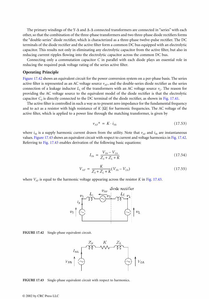
The primary windings of the Y-∆ and ∆-∆ connected transformers are connected in “series” with eachother, so that the combination of the three-phase transformers and two three-phase diode rectifiers formsthe “double-series” diode rectifier, which is characterized as a three-phase twelve-pulse rectifier. The DCterminals of the diode rectifier and the active filter form a common DC bus equipped with an electrolyticcapacitor. This results not only in eliminating any electrolytic capacitor from the active filter, but also inreducing current ripples flowing into the electrolytic capacitor across the common DC bus.
Connecting only a commutation capacitor C in parallel with each diode plays an essential role inreducing the required peak voltage rating of the series active filter.
Operating Principle
Figure 17.42 shows an equivalent circuit for the power conversion system on a per-phase basis. The seriesactive filter is represented as an AC voltage source vAF , and the double-series diode rectifier as the seriesconnection of a leakage inductor LL of the transformers with an AC voltage source vL. The reason forproviding the AC voltage source to the equivalent model of the diode rectifier is that the electrolyticcapacitor Cd is directly connected to the DC terminal of the diode rectifier, as shown in Fig. 17.41.
The active filter is controlled in such a way as to present zero impedance for the fundamental frequencyand to act as a resistor with high resistance of K [Ω] for harmonic frequencies. The AC voltage of theactive filter, which is applied to a power line through the matching transformer, is given by
(17.53)
where iSh is a supply harmonic current drawn from the utility. Note that vAF and iSh are instantaneousvalues. Figure 17.43 shows an equivalent circuit with respect to current and voltage harmonics in Fig. 17.42.Referring to Fig. 17.43 enables derivation of the following basic equations:
(17.54)
(17.55)
where VAF is equal to the harmonic voltage appearing across the resistor K in Fig. 17.43.
FIGURE 17.42 Single-phase equivalent circuit.
FIGURE 17.43 Single-phase equivalent circuit with respect to harmonics.
vAF∗ K iSh⋅=
ISh
VSh VLh–ZS ZL K+ +---------------------------=
VAFK
ZS ZL K+ +--------------------------- VSh VLh–( )=
© 2002 by CRC Press LLC
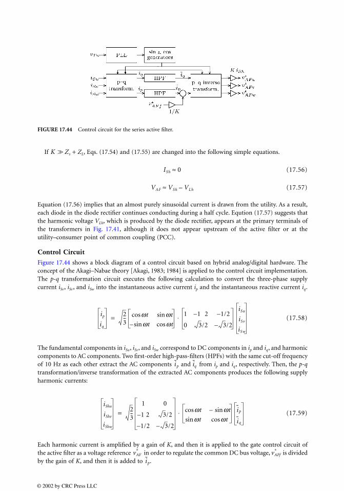
If + ZL, Eqs. (17.54) and (17.55) are changed into the following simple equations.
(17.56)
(17.57)
Equation (17.56) implies that an almost purely sinusoidal current is drawn from the utility. As a result,each diode in the diode rectifier continues conducting during a half cycle. Eqution (17.57) suggests thatthe harmonic voltage VLh, which is produced by the diode rectifier, appears at the primary terminals ofthe transformers in Fig. 17.41, although it does not appear upstream of the active filter or at theutility–consumer point of common coupling (PCC).
Control Circuit
Figure 17.44 shows a block diagram of a control circuit based on hybrid analog/digital hardware. Theconcept of the Akagi–Nabae theory [Akagi, 1983; 1984] is applied to the control circuit implementation.The p-q transformation circuit executes the following calculation to convert the three-phase supplycurrent iSv, iSv, and iSw into the instantaneous active current ip and the instantaneous reactive current iq.
(17.58)
The fundamental components in iSu, iSv, and iSw correspond to DC components in ip and iq, and harmoniccomponents to AC components. Two first-order high-pass-filters (HPFs) with the same cut-off frequencyof 10 Hz as each other extract the AC components and from ip and iq, respectively. Then, the p-qtransformation/inverse transformation of the extracted AC components produces the following supplyharmonic currents:
(17.59)
Each harmonic current is amplified by a gain of K, and then it is applied to the gate control circuit ofthe active filter as a voltage reference in order to regulate the common DC bus voltage, is dividedby the gain of K, and then it is added to .
FIGURE 17.44 Control circuit for the series active filter.
K >> Zs
ISh 0≈
VAF VSh VLh–≈
ip
iq
23-- wtcos wtsin
wtsin– wtcos
1 1 2– 1/2–
0 3/2 3/2–
iSu
iSv
iSw
⋅=
i p iq
iShu
iShv
iShw
23--
1 0
1 2– 3/2
1/2– 3/2–
wtcos wtsin–
wtsin wtcos
i p
iq
⋅=
vAF∗ vAFf
∗
i p
© 2002 by CRC Press LLC
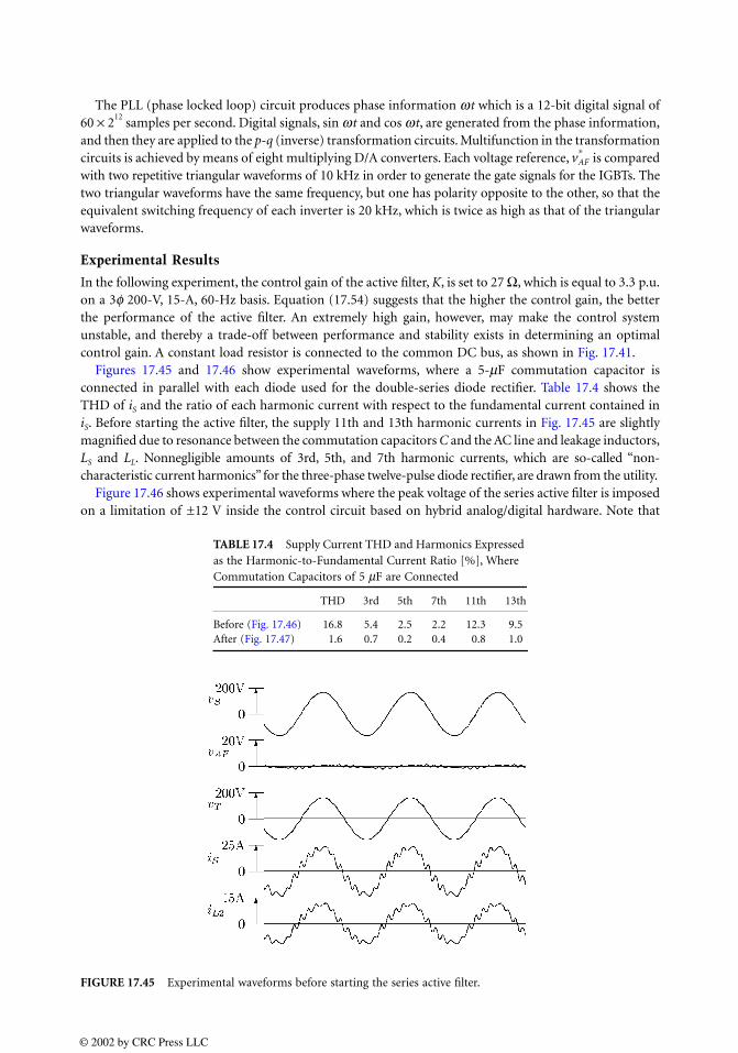
The PLL (phase locked loop) circuit produces phase information ωt which is a 12-bit digital signal of60 × 2
12 samples per second. Digital signals, sin ωt and cos ωt, are generated from the phase information,
and then they are applied to the p-q (inverse) transformation circuits. Multifunction in the transformationcircuits is achieved by means of eight multiplying D/A converters. Each voltage reference, is comparedwith two repetitive triangular waveforms of 10 kHz in order to generate the gate signals for the IGBTs. Thetwo triangular waveforms have the same frequency, but one has polarity opposite to the other, so that theequivalent switching frequency of each inverter is 20 kHz, which is twice as high as that of the triangularwaveforms.
Experimental Results
In the following experiment, the control gain of the active filter, K, is set to 27 Ω, which is equal to 3.3 p.u.on a 3φ 200-V, 15-A, 60-Hz basis. Equation (17.54) suggests that the higher the control gain, the betterthe performance of the active filter. An extremely high gain, however, may make the control systemunstable, and thereby a trade-off between performance and stability exists in determining an optimalcontrol gain. A constant load resistor is connected to the common DC bus, as shown in Fig. 17.41.
Figures 17.45 and 17.46 show experimental waveforms, where a 5-µF commutation capacitor isconnected in parallel with each diode used for the double-series diode rectifier. Table 17.4 shows theTHD of iS and the ratio of each harmonic current with respect to the fundamental current contained iniS. Before starting the active filter, the supply 11th and 13th harmonic currents in Fig. 17.45 are slightlymagnified due to resonance between the commutation capacitors C and the AC line and leakage inductors,LS and LL. Nonnegligible amounts of 3rd, 5th, and 7th harmonic currents, which are so-called “non-characteristic current harmonics” for the three-phase twelve-pulse diode rectifier, are drawn from the utility.
Figure 17.46 shows experimental waveforms where the peak voltage of the series active filter is imposedon a limitation of ±12 V inside the control circuit based on hybrid analog/digital hardware. Note that
TABLE 17.4 Supply Current THD and Harmonics Expressed as the Harmonic-to-Fundamental Current Ratio [%], Where Commutation Capacitors of 5 µF are Connected
THD 3rd 5th 7th 11th 13th
Before (Fig. 17.46) 16.8 5.4 2.5 2.2 12.3 9.5After (Fig. 17.47) 1.6 0.7 0.2 0.4 0.8 1.0
FIGURE 17.45 Experimental waveforms before starting the series active filter.
vAF∗
© 2002 by CRC Press LLC
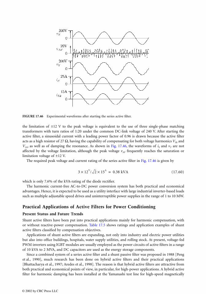
the limitation of ±12 V to the peak voltage is equivalent to the use of three single-phase matchingtransformers with turn ratios of 1:20 under the common DC-link voltage of 240 V. After starting theactive filter, a sinusoidal current with a leading power factor of 0.96 is drawn because the active filteracts as a high resistor of 27 Ω, having the capability of compensating for both voltage harmonics VSh andVLh, as well as of damping the resonance. As shown in Fig. 17.46, the waveforms of iS and vT are notaffected by the voltage limitation, although the peak voltage vAF frequently reaches the saturation orlimitation voltage of ±12 V.
The required peak voltage and current rating of the series active filter in Fig. 17.46 is given by
(17.60)
which is only 7.6% of the kVA-rating of the diode rectifier.The harmonic current-free AC-to-DC power conversion system has both practical and economical
advantages. Hence, it is expected to be used as a utility interface with large industrial inverter-based loadssuch as multiple adjustable speed drives and uninterruptible power supplies in the range of 1 to 10 MW.
Practical Applications of Active Filters for Power Conditioning
Present Status and Future Trends
Shunt active filters have been put into practical applications mainly for harmonic compensation, withor without reactive-power compensation. Table 17.5 shows ratings and application examples of shuntactive filters classified by compensation objectives.
Applications of shunt active filters are expanding, not only into industry and electric power utilitiesbut also into office buildings, hospitals, water supply utilities, and rolling stock. At present, voltage-fedPWM inverters using IGBT modules are usually employed as the power circuits of active filters in a rangeof 10 kVA to 2 MVA, and DC capacitors are used as the energy storage components.
Since a combined system of a series active filter and a shunt passive filter was proposed in 1988 [Penget al., 1990], much research has been done on hybrid active filters and their practical applications[Bhattacharya et al., 1997; Aredes et al., 1998]. The reason is that hybrid active filters are attractive fromboth practical and economical points of view, in particular, for high-power applications. A hybrid activefilter for harmonic damping has been installed at the Yamanashi test line for high-speed magnetically
FIGURE 17.46 Experimental waveforms after starting the series active filter.
3 12V× / 2 15A× 0.38 kVA=
© 2002 by CRC Press LLC
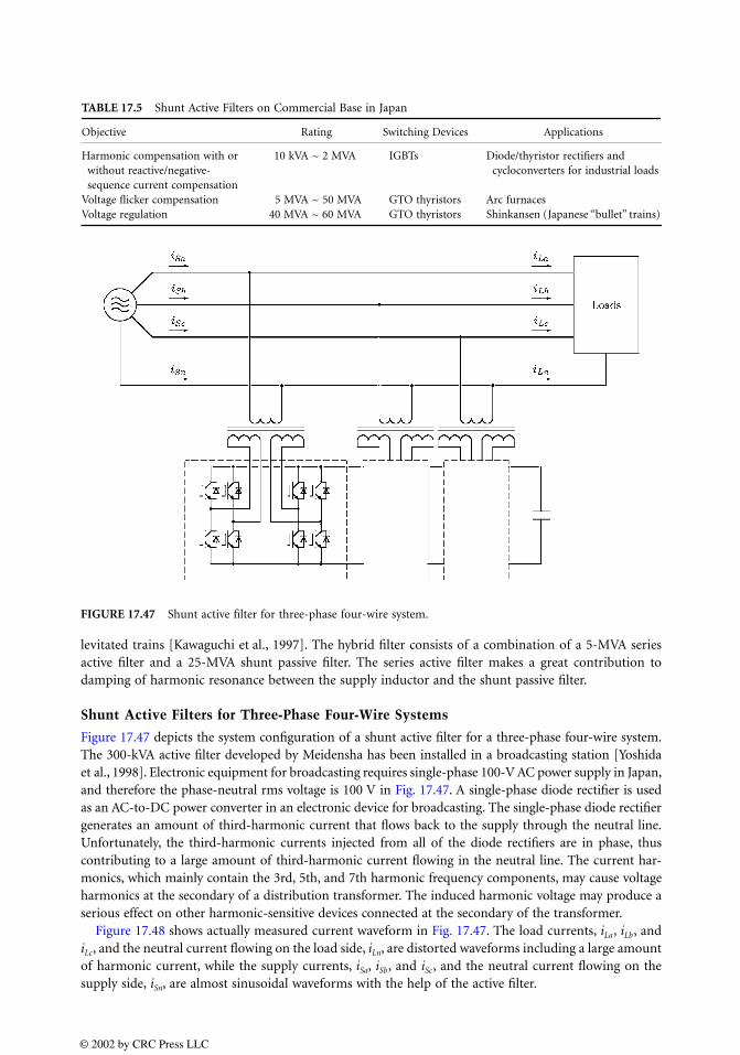
levitated trains [Kawaguchi et al., 1997]. The hybrid filter consists of a combination of a 5-MVA seriesactive filter and a 25-MVA shunt passive filter. The series active filter makes a great contribution todamping of harmonic resonance between the supply inductor and the shunt passive filter.
Shunt Active Filters for Three-Phase Four-Wire Systems
Figure 17.47 depicts the system configuration of a shunt active filter for a three-phase four-wire system.The 300-kVA active filter developed by Meidensha has been installed in a broadcasting station [Yoshidaet al., 1998]. Electronic equipment for broadcasting requires single-phase 100-V AC power supply in Japan,and therefore the phase-neutral rms voltage is 100 V in Fig. 17.47. A single-phase diode rectifier is usedas an AC-to-DC power converter in an electronic device for broadcasting. The single-phase diode rectifiergenerates an amount of third-harmonic current that flows back to the supply through the neutral line.Unfortunately, the third-harmonic currents injected from all of the diode rectifiers are in phase, thuscontributing to a large amount of third-harmonic current flowing in the neutral line. The current har-monics, which mainly contain the 3rd, 5th, and 7th harmonic frequency components, may cause voltageharmonics at the secondary of a distribution transformer. The induced harmonic voltage may produce aserious effect on other harmonic-sensitive devices connected at the secondary of the transformer.
Figure 17.48 shows actually measured current waveform in Fig. 17.47. The load currents, iLa, iLb, andiLc, and the neutral current flowing on the load side, iLn, are distorted waveforms including a large amountof harmonic current, while the supply currents, iSa, iSb, and iSc, and the neutral current flowing on thesupply side, iSn, are almost sinusoidal waveforms with the help of the active filter.
TABLE 17.5 Shunt Active Filters on Commercial Base in Japan
Objective Rating Switching Devices Applications
Harmonic compensation with or without reactive/negative-sequence current compensation
10 kVA ~ 2 MVA IGBTs Diode/thyristor rectifiers and cycloconverters for industrial loads
Voltage flicker compensation 5 MVA ~ 50 MVA GTO thyristors Arc furnacesVoltage regulation 40 MVA ~ 60 MVA GTO thyristors Shinkansen (Japanese “bullet” trains)
FIGURE 17.47 Shunt active filter for three-phase four-wire system.
© 2002 by CRC Press LLC
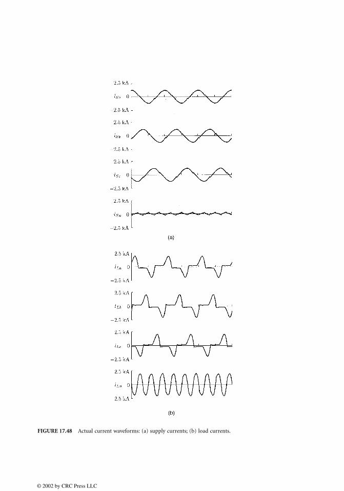
FIGURE 17.48 Actual current waveforms: (a) supply currents; (b) load currents.
© 2002 by CRC Press LLC
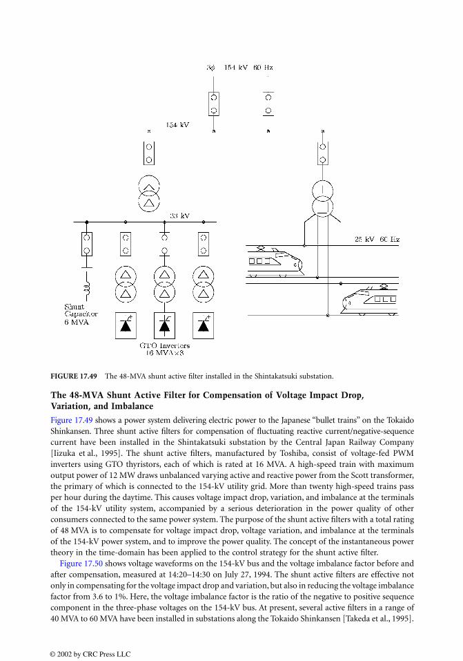
The 48-MVA Shunt Active Filter for Compensation of Voltage Impact Drop, Variation, and Imbalance
Figure 17.49 shows a power system delivering electric power to the Japanese “bullet trains” on the TokaidoShinkansen. Three shunt active filters for compensation of fluctuating reactive current/negative-sequencecurrent have been installed in the Shintakatsuki substation by the Central Japan Railway Company[Iizuka et al., 1995]. The shunt active filters, manufactured by Toshiba, consist of voltage-fed PWMinverters using GTO thyristors, each of which is rated at 16 MVA. A high-speed train with maximumoutput power of 12 MW draws unbalanced varying active and reactive power from the Scott transformer,the primary of which is connected to the 154-kV utility grid. More than twenty high-speed trains passper hour during the daytime. This causes voltage impact drop, variation, and imbalance at the terminalsof the 154-kV utility system, accompanied by a serious deterioration in the power quality of otherconsumers connected to the same power system. The purpose of the shunt active filters with a total ratingof 48 MVA is to compensate for voltage impact drop, voltage variation, and imbalance at the terminalsof the 154-kV power system, and to improve the power quality. The concept of the instantaneous powertheory in the time-domain has been applied to the control strategy for the shunt active filter.
Figure 17.50 shows voltage waveforms on the 154-kV bus and the voltage imbalance factor before andafter compensation, measured at 14:20–14:30 on July 27, 1994. The shunt active filters are effective notonly in compensating for the voltage impact drop and variation, but also in reducing the voltage imbalancefactor from 3.6 to 1%. Here, the voltage imbalance factor is the ratio of the negative to positive sequencecomponent in the three-phase voltages on the 154-kV bus. At present, several active filters in a range of40 MVA to 60 MVA have been installed in substations along the Tokaido Shinkansen [Takeda et al., 1995].
FIGURE 17.49 The 48-MVA shunt active filter installed in the Shintakatsuki substation.
© 2002 by CRC Press LLC
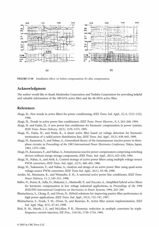
Acknowledgment
The author would like to thank Meidensha Corporation and Toshiba Corporation for providing helpfuland valuable information of the 300-kVA active filter and the 48-MVA active filter.
References
Akagi, H., New trends in active filters for power conditioning, IEEE Trans. Ind. Appl., 32, 6, 1312–1322,1996.
Akagi, H., Trends in active power line conditioners, IEEE Trans. Power Electron., 9, 3, 263–268, 1994.Akagi, H. and Fujita, H., A new power line conditioner for harmonic compensation in power systems,
IEEE Trans. Power Delivery, 10(3), 1570–1575, 1995.Akagi, H., Fujita, H., and Wada, K., A shunt active filter based on voltage detection for harmonic
termination of a radial power distribution line, IEEE Trans. Ind. Appl., 35(3), 638–645, 1999.Akagi, H., Kanazawa, Y., and Nabae, A., Generalized theory of the instantaneous reactive power in three-
phase circuits, in Proceedings of the 1983 International Power Electronics Conference, Tokyo, Japan,1983, 1375–1386.
Akagi, H., Kanazawa, Y., and Nabae, A., Instantaneous reactive power compensators comprising switchingdevices without energy storage components, IEEE Trans. Ind. Appl., 20(3), 625–630, 1984.
Akagi, H., Nabae, A., and Atoh, S., Control strategy of active power filters using multiple voltage-sourcePWM converters, IEEE Trans. Ind. Appl., 22(3), 460–465, 1986.
Akagi, H., Tsukamoto, Y., and Nabae, A., Analysis and design of an active power filter using quad-seriesvoltage-source PWM converters, IEEE Trans Ind. Appl., 26(1), 93–98, 1990.
Aredes, M., Heumann, K., and Watanabe, E. H., A universal active power line conditioner, IEEE Trans.Power Delivery, 13, 2, 545–551, 1998.
Balbo, N., Penzo, R., Sella, D., Malesani, L., Mattavelli, P., and Zuccato, A., Simplified hybrid active filtersfor harmonic compensation in low voltage industrial applications, in Proceedings of the 1994IEEE/PES International Conference on Harmonics in Power Systems, 1994, 263–269.
Bhattacharya, S., Cheng, P., and Divan, D., Hybrid solutions for improving passive filter performance inhigh power applications, IEEE Trans. Ind. Appl., 33(3), 732–747, 1997.
Bhattacharya, S., Frank, T. M., Divan, D., and Banerjee, B., Active filter system implementation, IEEEInd. Appl. Mag., 4(5), 47–63, 1998.
Bird, B. M., Marsh, J. F., and McLellan, P. R., Harmonic reduction in multiple converters by triple-frequency current injection, IEE Proc., 116(10), 1730–1734, 1969.
FIGURE 17.50 Installation effect: (a) before compensation; (b) after compensation.
© 2002 by CRC Press LLC

Fujita, H. and Akagi, H., An approach to harmonic current-free AC/DC power conversion for largeindustrial loads: the integration of a series active filter and a double-series diode rectifier, IEEETrans. Ind. Appl., 33(5), 1233–1240, 1997.
Fujita, H. and Akagi, H., A practical approach to harmonic compensation in power systems—seriesconnection of passive and active filters, IEEE Trans. Ind. Appl., 27(6), 1020–1025, 1991.
Fujita, H. and Akagi, H., The unified power quality conditioner: the integration of series- and shunt-active filters, IEEE Trans. Power Electron., 13(2), 315–322, 1998.
Grady, W. M., Samotyj, M. J., and Noyola, A. H., Survey of active power line conditioning methodologies,IEEE Trans. Power Delivery, 5(3), 1536–1542, 1990.
Gyugyi, L. and Strycula, E. C., Active AC power filters, in Proceedings of the 1976 IEEE/IAS Annual Meeting,1976, 529–535.
Iizuka, A., Kishida, M., Mochinaga, Y., Uzuka, T., Hirakawa, K., Aoyama, F., and Masuyama, T., Self-commutated static var generators at Shintakatsuki substation, in Proceedings of the 1995 Interna-tional Power Electronics Conference, Yokohama, Japan, 1995, 609–614.
Kawaguchi, I., Ikeda, H., Ogihara, Y., Syogaki, M., and Morita, H., Novel active filter system composedof inverter bypass circuit for suppression of harmonic resonance at the Yamanashi maglev test line,in Proceedings of the IEEE-IEEJ/IAS Power Conversion Conference, 1997, 175–180.
Kawahira, H., Nakamura, T., Nakazawa, S., and Nomura, M., Active power filters, in Proceedings of the1983 International Power Electronics Conference, Tokyo, Japan, 1983, 981–992.
Krah, J. O. and Holtz, J., Total compensation of line-side switching harmonics in converter-fed AClocomotives, in Proceedings of the 1994 IEEE/IAS Annual Meeting, 1994, 913–920.
Lee, T-N., Pereira, M., Renz, K., and Vaupel, G., Active damping of resonances in power systems, IEEETrans. Power Delivery, 9(2), 1001–1008, 1994.
Moran, S., A line voltage regulator/conditioner for harmonic-sensitive load isolation, in Proceedings ofthe 1989 IEEE/IAS Annual Meeting, 1989, 947–951.
Peng, F. Z., Application issues of active power filters, IEEE Ind. Appl. Mag., 4(5), 21–30, 1998.Peng, F. Z., Akagi, H., and Nabae, A., Compensation characteristics of the combined system of shunt
passive and series active filters, IEEE Trans. Ind. Appl., 29(1), 144–152, 1993.Peng, F. Z., Akagi, H., and Nabae, A., A new approach to harmonic compensation in power systems—
a combined system of shunt passive and series active filters, IEEE Trans. Ind. Appl., 26(6), 983–990,1990.
Peng, F. Z., Akagi, H., and Nabae, A., A study of active power filters using quad-series voltage-sourcePWM converters for harmonic compensation, IEEE Trans. Power Electron., 5(1), 9–15, 1990.
Takeda, M., Murakami, S., Iizuka, A., Kishida, M., Mochinaga, Y., Hase, S., and Mochinaga, H., Devel-opment of an SVG series for voltage control over three-phase unbalance caused by railway load,in Proceedings of the 1995 International Power Electronics Conference, Yokohama, Japan, 1995,603–608.
Takeda, M., Ikeda, K., and Tominaga, Y., Harmonic current compensation with active filter, in Proceedingsof the 1987 IEEE/IAS Annual Meeting, 1987, 808–815.
Van Schoor, G. and van Wyk, J., A study of a system of a current-fed converters as an active three-phasefilter, in Proceedings of the 1987 IEEE/PELS Power Electronics Specialist Conference, 1987, 482–490.
Van Zyl, A., Enslin, J. H. R., and Spée, R., Converter based solution to power quality problems on radialdistribution lines, in Proceedings of the 1995 IEEE/IAS Annual Meeting, 1995, 2573–2580.
Watanabe, E. H., Series active filter for the DC side of HVDC transmission systems, in Proceedings of the1990 International Power Electronics Conference, Tokyo, Japan, 1990, 1024–1030.
Yoshida, T., Nakagawa, G., Kitamura, H., and Iwatani, K., Active filters (multi-functional harmonicsuppressors) used to protect the quality of power supply from harmonics and reactive powergenerated in loads, Meiden Rev., 262(5), 13–17, 1998 (in Japanese).
Zhang, W., Asplund, G.,.Aberg, A., Jonsson, U., and Lööf, O., Active DC filter for HVDC system—A test
installation in the Konti-Skan at Lindome converter station, IEEE Trans. Power Delivery, 8(3),1599–1605, 1993.
© 2002 by CRC Press LLC
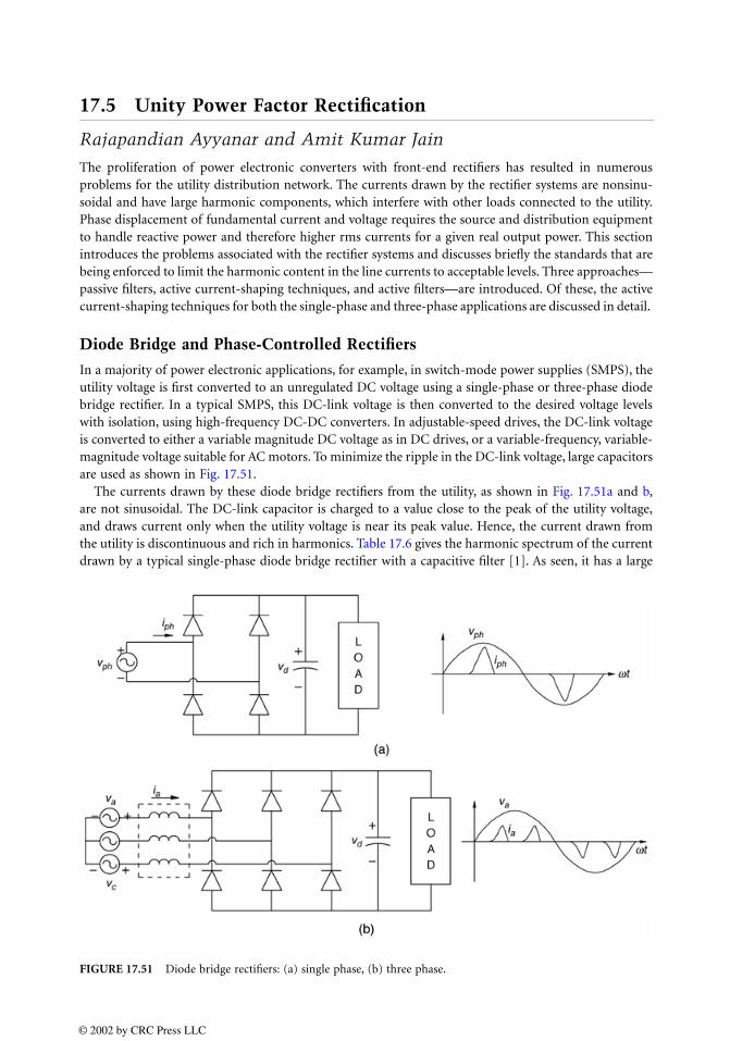
17.5 Unity Power Factor Rectification
Rajapandian Ayyanar and Amit Kumar Jain
The proliferation of power electronic converters with front-end rectifiers has resulted in numerousproblems for the utility distribution network. The currents drawn by the rectifier systems are nonsinu-soidal and have large harmonic components, which interfere with other loads connected to the utility.Phase displacement of fundamental current and voltage requires the source and distribution equipmentto handle reactive power and therefore higher rms currents for a given real output power. This sectionintroduces the problems associated with the rectifier systems and discusses briefly the standards that arebeing enforced to limit the harmonic content in the line currents to acceptable levels. Three approaches—passive filters, active current-shaping techniques, and active filters—are introduced. Of these, the activecurrent-shaping techniques for both the single-phase and three-phase applications are discussed in detail.
Diode Bridge and Phase-Controlled Rectifiers
In a majority of power electronic applications, for example, in switch-mode power supplies (SMPS), theutility voltage is first converted to an unregulated DC voltage using a single-phase or three-phase diodebridge rectifier. In a typical SMPS, this DC-link voltage is then converted to the desired voltage levelswith isolation, using high-frequency DC-DC converters. In adjustable-speed drives, the DC-link voltageis converted to either a variable magnitude DC voltage as in DC drives, or a variable-frequency, variable-magnitude voltage suitable for AC motors. To minimize the ripple in the DC-link voltage, large capacitorsare used as shown in Fig. 17.51.
The currents drawn by these diode bridge rectifiers from the utility, as shown in Fig. 17.51a and b,are not sinusoidal. The DC-link capacitor is charged to a value close to the peak of the utility voltage,and draws current only when the utility voltage is near its peak value. Hence, the current drawn fromthe utility is discontinuous and rich in harmonics. Table 17.6 gives the harmonic spectrum of the currentdrawn by a typical single-phase diode bridge rectifier with a capacitive filter [1]. As seen, it has a large
FIGURE 17.51 Diode bridge rectifiers: (a) single phase, (b) three phase.
© 2002 by CRC Press LLC
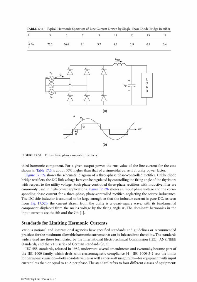
third harmonic component. For a given output power, the rms value of the line current for the caseshown in Table 17.6 is about 30% higher than that of a sinusoidal current at unity power factor.
Figure 17.52a shows the schematic diagram of a three-phase phase-controlled rectifier. Unlike diodebridge rectifiers, the DC-link voltage here can be regulated by controlling the firing angle of the thyristorswith respect to the utility voltage. Such phase-controlled three-phase rectifiers with inductive filter arecommonly used in high-power applications. Figure 17.52b shows an input phase voltage and the corre-sponding phase current for a three-phase, phase-controlled rectifier, neglecting the source inductance.The DC side inductor is assumed to be large enough so that the inductor current is pure DC. As seenfrom Fig. 17.52b, the current drawn from the utility is a quasi-square wave, with its fundamentalcomponent displaced from the mains voltage by the firing angle α . The dominant harmonics in theinput currents are the 5th and the 7th [1].
Standards for Limiting Harmonic Currents
Various national and international agencies have specified standards and guidelines or recommendedpractices for the maximum allowable harmonic currents that can be injected into the utility. The standardswidely used are those formulated by the International Electrotechnical Commission (IEC), ANSI/IEEEStandards, and the VDE series of German standards [2, 3].
IEC 555 standards, released in 1982, underwent several amendments and eventually became part ofthe IEC 1000 family, which deals with electromagnetic compliance [4]. IEC 1000-3-2 sets the limitsfor harmonic emission—both absolute values as well as per-watt magnitude—for equipment with inputcurrent less than or equal to 16 A per phase. The standard refers to four different classes of equipment:
TABLE 17.6 Typical Harmonic Spectrum of Line Current Drawn by Single-Phase Diode Bridge Rectifier
h 3 5 7 9 11 13 15 17
% 73.2 36.6 8.1 5.7 4.1 2.9 0.8 0.4
FIGURE 17.52 Three-phase phase-controlled rectifiers.
Ih
I1
----
© 2002 by CRC Press LLC
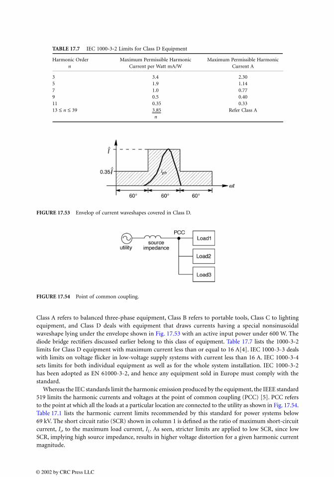
Class A refers to balanced three-phase equipment, Class B refers to portable tools, Class C to lightingequipment, and Class D deals with equipment that draws currents having a special nonsinusoidalwaveshape lying under the envelope shown in Fig. 17.53 with an active input power under 600 W. Thediode bridge rectifiers discussed earlier belong to this class of equipment. Table 17.7 lists the 1000-3-2limits for Class D equipment with maximum current less than or equal to 16 A[4]. IEC 1000-3-3 dealswith limits on voltage flicker in low-voltage supply systems with current less than 16 A. IEC 1000-3-4sets limits for both individual equipment as well as for the whole system installation. IEC 1000-3-2has been adopted as EN 61000-3-2, and hence any equipment sold in Europe must comply with thestandard.
Whereas the IEC standards limit the harmonic emission produced by the equipment, the IEEE standard519 limits the harmonic currents and voltages at the point of common coupling (PCC) [5]. PCC refersto the point at which all the loads at a particular location are connected to the utility as shown in Fig. 17.54.Table 17.1 lists the harmonic current limits recommended by this standard for power systems below69 kV. The short circuit ratio (SCR) shown in column 1 is defined as the ratio of maximum short-circuitcurrent, Is, to the maximum load current, IL. As seen, stricter limits are applied to low SCR, since lowSCR, implying high source impedance, results in higher voltage distortion for a given harmonic currentmagnitude.
TABLE 17.7 IEC 1000-3-2 Limits for Class D Equipment
Harmonic Ordern
Maximum Permissible Harmonic Current per Watt mA/W
Maximum Permissible Harmonic Current A
3 3.4 2.305 1.9 1.147 1.0 0.779 0.5 0.4011 0.35 0.3313 ≤ n ≤ 39 3.85 Refer Class A
n
FIGURE 17.53 Envelop of current waveshapes covered in Class D.
FIGURE 17.54 Point of common coupling.
© 2002 by CRC Press LLC
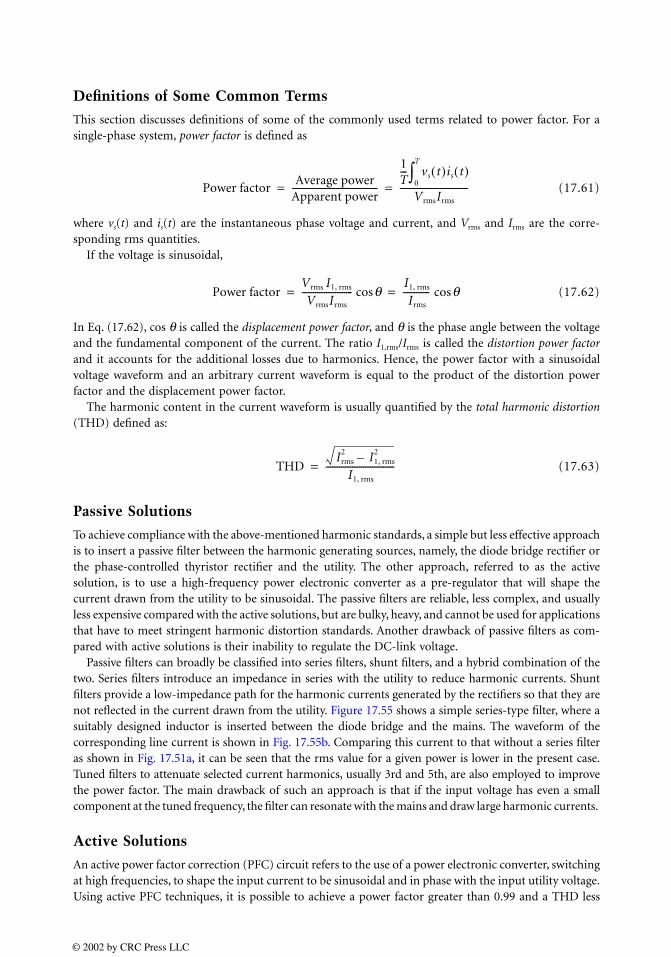
Definitions of Some Common Terms
This section discusses definitions of some of the commonly used terms related to power factor. For asingle-phase system, power factor is defined as
(17.61)
where vs(t) and is(t) are the instantaneous phase voltage and current, and Vrms and Irms are the corre-sponding rms quantities.
If the voltage is sinusoidal,
(17.62)
In Eq. (17.62), cos θ is called the displacement power factor, and θ is the phase angle between the voltageand the fundamental component of the current. The ratio I1,rms/Irms is called the distortion power factorand it accounts for the additional losses due to harmonics. Hence, the power factor with a sinusoidalvoltage waveform and an arbitrary current waveform is equal to the product of the distortion powerfactor and the displacement power factor.
The harmonic content in the current waveform is usually quantified by the total harmonic distortion(THD) defined as:
(17.63)
Passive Solutions
To achieve compliance with the above-mentioned harmonic standards, a simple but less effective approachis to insert a passive filter between the harmonic generating sources, namely, the diode bridge rectifier orthe phase-controlled thyristor rectifier and the utility. The other approach, referred to as the activesolution, is to use a high-frequency power electronic converter as a pre-regulator that will shape thecurrent drawn from the utility to be sinusoidal. The passive filters are reliable, less complex, and usuallyless expensive compared with the active solutions, but are bulky, heavy, and cannot be used for applicationsthat have to meet stringent harmonic distortion standards. Another drawback of passive filters as com-pared with active solutions is their inability to regulate the DC-link voltage.
Passive filters can broadly be classified into series filters, shunt filters, and a hybrid combination of thetwo. Series filters introduce an impedance in series with the utility to reduce harmonic currents. Shuntfilters provide a low-impedance path for the harmonic currents generated by the rectifiers so that they arenot reflected in the current drawn from the utility. Figure 17.55 shows a simple series-type filter, where asuitably designed inductor is inserted between the diode bridge and the mains. The waveform of thecorresponding line current is shown in Fig. 17.55b. Comparing this current to that without a series filteras shown in Fig. 17.51a, it can be seen that the rms value for a given power is lower in the present case.Tuned filters to attenuate selected current harmonics, usually 3rd and 5th, are also employed to improvethe power factor. The main drawback of such an approach is that if the input voltage has even a smallcomponent at the tuned frequency, the filter can resonate with the mains and draw large harmonic currents.
Active Solutions
An active power factor correction (PFC) circuit refers to the use of a power electronic converter, switchingat high frequencies, to shape the input current to be sinusoidal and in phase with the input utility voltage.Using active PFC techniques, it is possible to achieve a power factor greater than 0.99 and a THD less
Power factorAverage power
Apparent power---------------------------------------
1T--- vs t( )is t( )
0
T
∫VrmsIrms
-------------------------------= =
Power factorVrms I1, rms
VrmsIrms
----------------------- qcosI1, rms
Irms
------------ qcos= =
THDIrms
2 I1, rms2–
I1, rms
-------------------------------=
© 2002 by CRC Press LLC
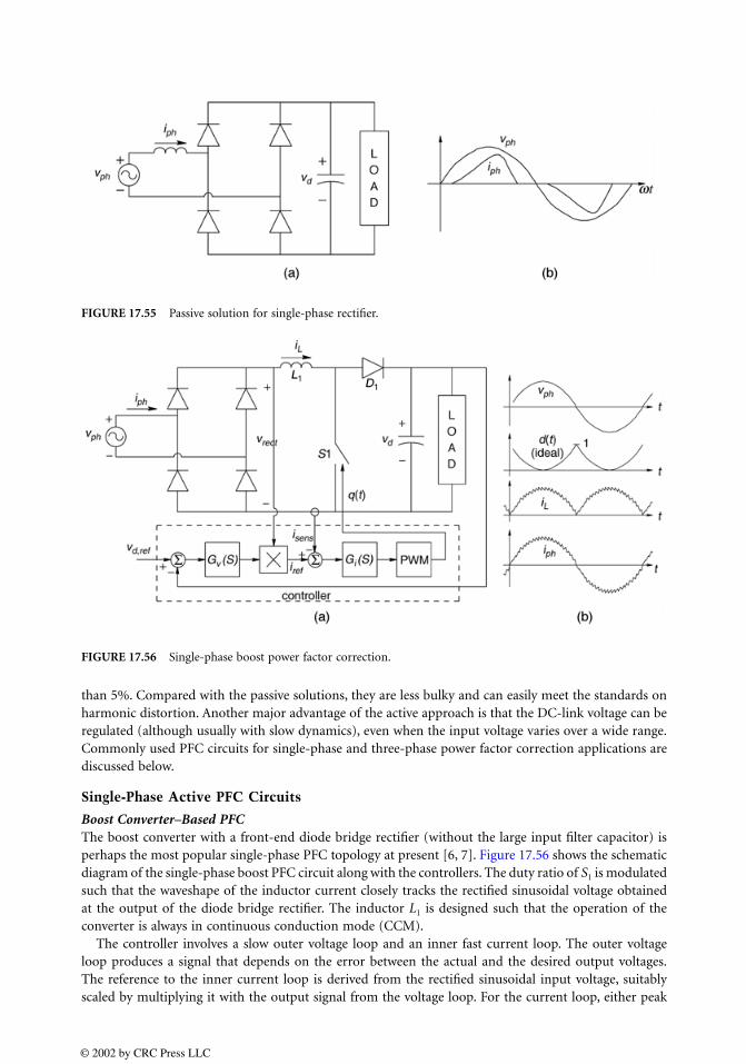
than 5%. Compared with the passive solutions, they are less bulky and can easily meet the standards onharmonic distortion. Another major advantage of the active approach is that the DC-link voltage can beregulated (although usually with slow dynamics), even when the input voltage varies over a wide range.Commonly used PFC circuits for single-phase and three-phase power factor correction applications arediscussed below.
Single-Phase Active PFC Circuits
Boost Converter–Based PFCThe boost converter with a front-end diode bridge rectifier (without the large input filter capacitor) isperhaps the most popular single-phase PFC topology at present [6, 7]. Figure 17.56 shows the schematicdiagram of the single-phase boost PFC circuit along with the controllers. The duty ratio of S1 is modulatedsuch that the waveshape of the inductor current closely tracks the rectified sinusoidal voltage obtainedat the output of the diode bridge rectifier. The inductor L1 is designed such that the operation of theconverter is always in continuous conduction mode (CCM).
The controller involves a slow outer voltage loop and an inner fast current loop. The outer voltageloop produces a signal that depends on the error between the actual and the desired output voltages.The reference to the inner current loop is derived from the rectified sinusoidal input voltage, suitablyscaled by multiplying it with the output signal from the voltage loop. For the current loop, either peak
FIGURE 17.55 Passive solution for single-phase rectifier.
FIGURE 17.56 Single-phase boost power factor correction.
© 2002 by CRC Press LLC

current mode control or average current control can be used. In average current mode control, the currentcontroller amplifies the error between the actual inductor current and the current reference. This ampli-fied error signal is then compared with a fixed frequency ramp to obtain the gate control signal q(t) forthe switch. In peak current mode control, the actual inductor current iL(t) is compared with the currentreference, iref(t). When iL(t) just exceeds the reference the switch is turned off, and is turned on again at startof the next switching cycle by a fixed-frequency clock signal. It is also possible to control the current usinga hysteresis controller.
As in DC-DC converter applications, the output voltage of the boost converter needs to be above themaximum input voltage. Hence, for single-phase PFC applications using the boost converter, the DC-link voltage has to be higher than the peak of the maximum input utility voltage. For a nominal utilityvoltage of 110 V rms, the DC-link voltage needs to be close to 200 V DC. In a single-phase rectifier withunity power factor, the input power fluctuates at twice the fundamental frequency (for example, 120 Hz),whereas the output power is constant (within the 120-Hz cycle). Hence, energy storage elements areneeded to account for the difference between the instantaneous values of the input power and the outputpower. The output capacitor of the boost converter thus needs to be large in single-phase PFC applications.
Figure 17.56b shows the waveforms corresponding to the input utility voltage, the idealized instanta-neous switch duty ratio, the inductor current, and the current drawn from the utility. Usually small, low-pass filters are used to reduce the high-frequency switching component in the input current, and to meetEMI standards.
The design of the feedback controller for both the outer voltage loop and the inner current loop isdiscussed in detail in Refs. 6 and 7. The reference signal to the current loop, which is mainly a rectifiedsinusoidal voltage, contains a large second-order harmonic term, and substantial higher-order harmonics.Therefore, to obtain low THD for the input current, the current loop should be able to track the higher-order harmonics. Thus, the current loop should have a high bandwidth. This is especially important ifthe input frequency is higher, as, for example, 400 Hz in avionic applications.
The current through the filter capacitor has a large second harmonic component apart from theswitching frequency component. This is reflected in the DC-link voltage as large second harmonic ripplevoltage. The outer voltage loop therefore should be designed for low bandwidth (much less than 120 Hzfor utility applications) so that the above-mentioned ripple voltage does not distort the reference signalapplied to the current loop. Since voltage control is required to have a low bandwidth it does notcompensate for 120 Hz and the dynamic response for step-load changes is very poor. Usually the boostPFC is used as a pre-regulator with main emphasis on drawing sinusoidal currents at unity power factor.The pre-regulator is followed by a second-stage DC-DC converter, which provides electrical isolation aswell as good dynamic regulation of load voltage at any desired voltage levels.
Other CCM TopologiesSimilar to the boost converter, several other basic DC-DC converter topologies can be used with a diodebridge rectifier for PFC applications. SEPIC and Cúk converters operating in CCM have the sameadvantage as the boost converter in that they draw continuous current from the utility with small, high-frequency ripple [8]. An additional advantage of SEPIC or Cúk converter over the boost converter forPFC applications is that the output voltage can be less than the peak of the input voltage. The trade-offis in the complex controller design.
For single-phase PFC applications, buck-derived converters are not practical because such a converterwill not be able to draw any current from the input when the input voltage is instantaneously less thanthe output voltage. Figure 17.57 shows an interesting combination of a buck and a boost converter suitablefor PFC applications that require the output voltage to be less than the peak input voltage [9]. When themain voltage is instantaneously less than the desired output voltage, S1 is fully on, and the duty ratio ofS2 is controlled in response to the current reference. The operation is now in boost mode. When the inputvoltage is higher than the output, S2 is fully off and the duty ratio of S1 is controlled, and the operationis now in the buck mode. In the buck mode the input current is discontinuous, but its average valuetracks the input voltage.
© 2002 by CRC Press LLC
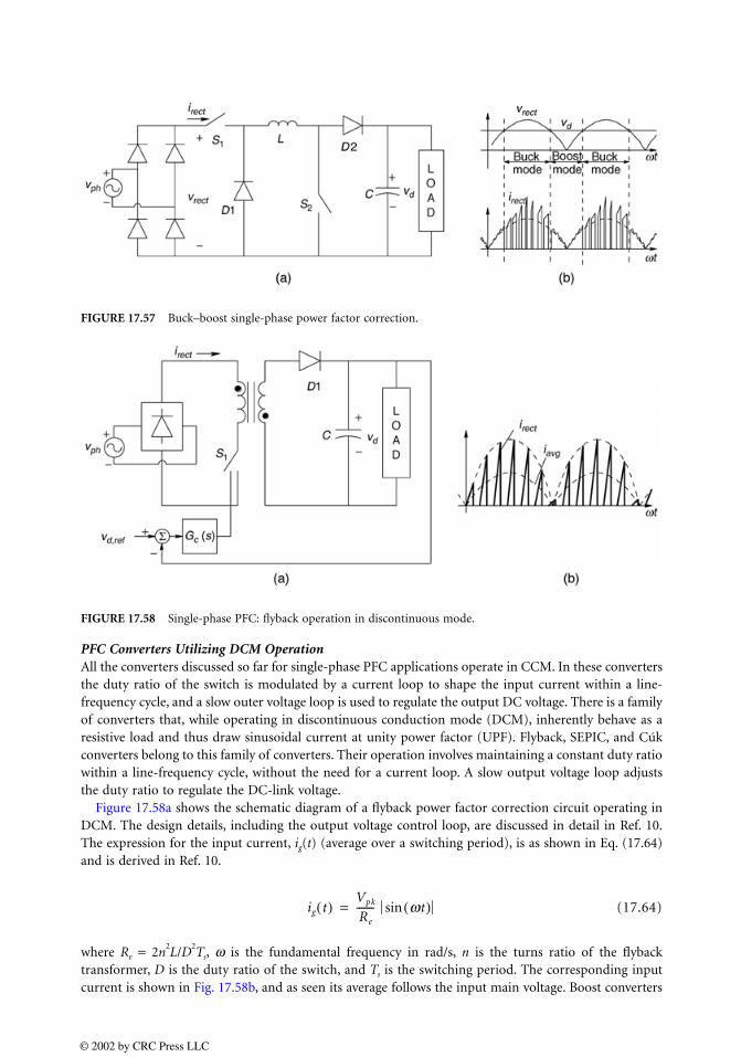
PFC Converters Utilizing DCM OperationAll the converters discussed so far for single-phase PFC applications operate in CCM. In these convertersthe duty ratio of the switch is modulated by a current loop to shape the input current within a line-frequency cycle, and a slow outer voltage loop is used to regulate the output DC voltage. There is a familyof converters that, while operating in discontinuous conduction mode (DCM), inherently behave as aresistive load and thus draw sinusoidal current at unity power factor (UPF). Flyback, SEPIC, and Cúkconverters belong to this family of converters. Their operation involves maintaining a constant duty ratiowithin a line-frequency cycle, without the need for a current loop. A slow output voltage loop adjuststhe duty ratio to regulate the DC-link voltage.
Figure 17.58a shows the schematic diagram of a flyback power factor correction circuit operating inDCM. The design details, including the output voltage control loop, are discussed in detail in Ref. 10.The expression for the input current, ig(t) (average over a switching period), is as shown in Eq. (17.64)and is derived in Ref. 10.
(17.64)
where Re = 2n2L/D
2Ts, ω is the fundamental frequency in rad/s, n is the turns ratio of the flyback
transformer, D is the duty ratio of the switch, and Ts is the switching period. The corresponding inputcurrent is shown in Fig. 17.58b, and as seen its average follows the input main voltage. Boost converters
FIGURE 17.57 Buck–boost single-phase power factor correction.
FIGURE 17.58 Single-phase PFC: flyback operation in discontinuous mode.
ig t( )Vpk
Re
------- wt( )sin=
© 2002 by CRC Press LLC
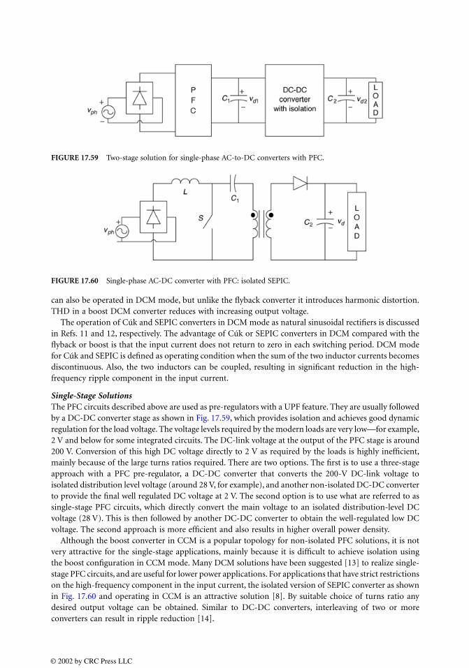
can also be operated in DCM mode, but unlike the flyback converter it introduces harmonic distortion.THD in a boost DCM converter reduces with increasing output voltage.
The operation of Cúk and SEPIC converters in DCM mode as natural sinusoidal rectifiers is discussedin Refs. 11 and 12, respectively. The advantage of Cúk or SEPIC converters in DCM compared with theflyback or boost is that the input current does not return to zero in each switching period. DCM modefor Cúk and SEPIC is defined as operating condition when the sum of the two inductor currents becomesdiscontinuous. Also, the two inductors can be coupled, resulting in significant reduction in the high-frequency ripple component in the input current.
Single-Stage SolutionsThe PFC circuits described above are used as pre-regulators with a UPF feature. They are usually followedby a DC-DC converter stage as shown in Fig. 17.59, which provides isolation and achieves good dynamicregulation for the load voltage. The voltage levels required by the modern loads are very low—for example,2 V and below for some integrated circuits. The DC-link voltage at the output of the PFC stage is around200 V. Conversion of this high DC voltage directly to 2 V as required by the loads is highly inefficient,mainly because of the large turns ratios required. There are two options. The first is to use a three-stageapproach with a PFC pre-regulator, a DC-DC converter that converts the 200-V DC-link voltage toisolated distribution level voltage (around 28 V, for example), and another non-isolated DC-DC converterto provide the final well regulated DC voltage at 2 V. The second option is to use what are referred to assingle-stage PFC circuits, which directly convert the main voltage to an isolated distribution-level DCvoltage (28 V). This is then followed by another DC-DC converter to obtain the well-regulated low DCvoltage. The second approach is more efficient and also results in higher overall power density.
Although the boost converter in CCM is a popular topology for non-isolated PFC solutions, it is notvery attractive for the single-stage applications, mainly because it is difficult to achieve isolation usingthe boost configuration in CCM mode. Many DCM solutions have been suggested [13] to realize single-stage PFC circuits, and are useful for lower power applications. For applications that have strict restrictionson the high-frequency component in the input current, the isolated version of SEPIC converter as shownin Fig. 17.60 and operating in CCM is an attractive solution [8]. By suitable choice of turns ratio anydesired output voltage can be obtained. Similar to DC-DC converters, interleaving of two or moreconverters can result in ripple reduction [14].
FIGURE 17.59 Two-stage solution for single-phase AC-to-DC converters with PFC.
FIGURE 17.60 Single-phase AC-DC converter with PFC: isolated SEPIC.
© 2002 by CRC Press LLC

Three-Phase PFC Circuits
At higher power levels, for example, above a few kilowatts, three-phase rectifiers are normally preferred.As in the case of single-phase rectifiers, passive PFC solutions are acceptable for less-demanding appli-cations. The passive solutions are typically bulkier. For applications with stringent restrictions on theallowable harmonic distortion active current shaping using high-frequency power electronic circuits isnecessary.
Six-Switch PWM ConvertersPerhaps the most effective, but expensive, solution is the six-switch boost PWM (pulse-width-modulated)converter [15] shown in Fig. 17.61. The design of the converter ensures that the operation is always inCCM. The control involves an outer voltage loop, which gives the reference to the inner current loop. Apreferred method of current control for the inner loop is to use space-vector modulation (SVM) tech-niques, with digital implementation. The output voltage needs to be higher than the peak of the inputline-to-line voltage [16]. A major advantage of the six-switch PWM boost rectifier is its bidirectionalpower flow capability. However, because of the higher cost and complex control requirement, its use islimited to higher power applications and applications requiring bidirectional power flow. Unlike single-phase converters, in all the three-phase PFC circuits, the power drawn from the input is not pulsating(at two or six times the fundamental frequency). Hence, the output capacitor can be designed based onjust the hold-up time requirement. Figure 17.62 shows the schematic diagram of a six-switch buck-derived PWM PFC circuit. The advantage of the buck-derived converter is that the output voltage canbe lower than the peak value of the input voltage. However, the input current is discontinuous, and hencelarge filters are needed to reduce the switching frequency component in the input current.
Single-Switch Three-Phase PFCsThe simplest active three-phase PFC circuit is the single-switch DCM boost converter shown in Fig. 17.63a[17]. The duty ratio S is kept constant within a line-frequency cycle, and is controlled by a slow, outervoltage loop. Because of DCM operation, all the three-phase currents are zero at the beginning of the
FIGURE 17.61 Three-phase six-switch boost PFC.
FIGURE 17.62 Three-phase six-switch buck PFC.
© 2002 by CRC Press LLC
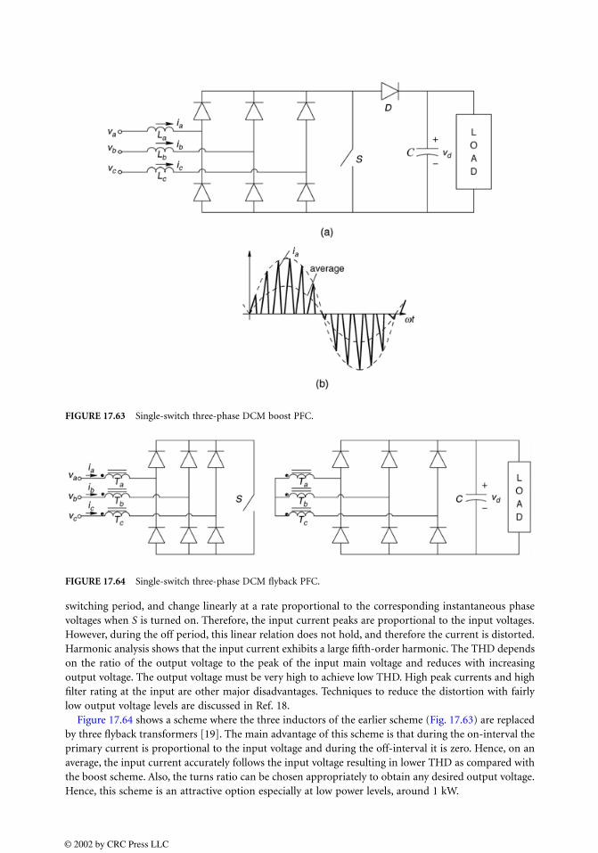
switching period, and change linearly at a rate proportional to the corresponding instantaneous phasevoltages when S is turned on. Therefore, the input current peaks are proportional to the input voltages.However, during the off period, this linear relation does not hold, and therefore the current is distorted.Harmonic analysis shows that the input current exhibits a large fifth-order harmonic. The THD dependson the ratio of the output voltage to the peak of the input main voltage and reduces with increasingoutput voltage. The output voltage must be very high to achieve low THD. High peak currents and highfilter rating at the input are other major disadvantages. Techniques to reduce the distortion with fairlylow output voltage levels are discussed in Ref. 18.
Figure 17.64 shows a scheme where the three inductors of the earlier scheme (Fig. 17.63) are replacedby three flyback transformers [19]. The main advantage of this scheme is that during the on-interval theprimary current is proportional to the input voltage and during the off-interval it is zero. Hence, on anaverage, the input current accurately follows the input voltage resulting in lower THD as compared withthe boost scheme. Also, the turns ratio can be chosen appropriately to obtain any desired output voltage.Hence, this scheme is an attractive option especially at low power levels, around 1 kW.
FIGURE 17.63 Single-switch three-phase DCM boost PFC.
FIGURE 17.64 Single-switch three-phase DCM flyback PFC.
© 2002 by CRC Press LLC

Figure 17.65 shows a representative topology from a class of multiresonant single-switch three-phasePFC circuits [20]. Low THD can be achieved with the additional advantage of soft-switching for themain switch. However, the VA rating of the switch is high for a given output power, and hence itsapplication is limited to lower power levels. Control of output voltage is achieved by varying the switchingfrequency. The operation is designed to be in discontinuous voltage mode (DVM) with respect to theinput capacitors, and the average voltage across the capacitors is proportional to the correspondinginstantaneous phase voltages.
Use of Single-Phase PFCs for Three-Phase ApplicationsAn attractive solution to achieve high-performance three-phase rectification is to use three single-phasePFC circuits connected in star or delta at the input side and in parallel at the output side. When non-isolated single-phase converters are used in such a scheme, precaution should be taken to avoid interactionamong the three phases. Ref. 21 discusses in detail the operation of three nonisolated boost PFC circuitswith extra circuitry to avoid phase interactions. The advantages include low overall switch ratings andlow passive component ratings compared with other solutions of similar performance. Also, well-knownsingle-phase PFC methods, as well as control ICs can be directly applied for the three-phase extension.
Figure 17.66 shows three isolated single-phase SEPIC converters operating in CCM, with delta con-nection at the input and parallel connection at the output [22]. Since the three single-phase PFCs areisolated, there is no problem of adverse interaction among the three phases, and hence it is an attractivesingle-stage solution.
Vienna RectifierA three-switch, three-level, three-phase PFC circuit referred to as Vienna rectifier [23] is shown in Fig. 17.67.The three switches are controlled usually by space-vector PWM such that the input currents accuratelytrack the phase voltages. When a switch is turned on, the corresponding phase is connected to themidpoint O, resulting in an increase in the phase current. Turning off the switch results in the conductionof the associated diodes in the upper or lower bridge half, causing the phase currents to reduce. Becauseof the inclusion of the midpoint of the output voltage into the system function, the circuit has three-level characteristics. Hence, the high-frequency content in the mains current is reduced significantly ascompared with that in the two-level converters. Another advantage is the relatively lower combined VAratings for the controllable switches. The disadvantage is the slightly more complex control circuitry.
Buck-Derived Three-Phase PFCFigure 17.68 shows the schematic diagram of two interleaved buck-derived three-phase PFC circuits withthree switches each. The control is very simple, as it is based on conventional sinusoidal PWM, andretains good harmonic performance [24]. The output voltage can be lower than the peak of the inputvoltage. However, the input currents are discontinuous, making it necessary to use large low-pass filtersat the input to attenuate the switching frequency content. As suggested in Fig. 17.68, two or more such
FIGURE 17.65 Single-switch three-phase buck-derived multiresonant ZSC PFC.
© 2002 by CRC Press LLC
buck-derived PFC circuits can be interleaved, i.e., connected in parallel with their switching signalssuitably sequenced. Interleaving leads to ripple cancellation, resulting in lower filter requirement.
Active Filters
Use of passive filters between the harmonic generating rectifier load and the utility is discussed brieflyin the section on passive solutions. The main drawbacks mentioned were that passive filters are bulky,can result in over/undercompensation as the load varies, and can result in a low-impedance current pathfor the harmonic components present in the utility voltage. In this section, another approach to reducethe harmonic distortion, namely, the active filters, is discussed [25, 26]. Figure 17.69 shows a blockdiagram representation of the concept of active filters to eliminate the harmonic currents from enteringthe utility. The current drawn by the rectifier system (single-phase or three-phase) has a fundamentalcomponent and a distortion component . The active filter senses the current drawn by therectifier system and, by high-frequency current-mode control, delivers the distortion component .Therefore, the utility needs to deliver only the fundamental component of the current drawn by therectifier system. Since the active filter needs to supply only the harmonic component of the current, noactive power needs to be delivered to the load by the active filter. Hence, the active filter does not requirea separate energy source. Figure 17.70 shows a typical implementation of an active filter for three-phasePFC applications. For high-power systems, where the use of active filter may be limited by the availabilityof high-voltage and high-current devices, hybrid filters, which are a combination of active filters andpassive LC filters, are an effective approach to meet harmonic standards.
FIGURE 17.66 Three single-phase SEPIC converters delta-connected at input and paralled at the ouptput.
iL1iLdistortion1
iLdistortion1
© 2002 by CRC Press LLC
FIGURE 17.67 Vienna rectifier–I.
FIGURE 17.68 Three-phase interleaved PFC.
© 2002 by CRC Press LLC
Summary
The input currents drawn by conventional diode bridge and phase-controlled thyristor rectifiers are far fromsinusoidal and are rich in harmonics. The harmonic currents pollute the utility system and interfere withother loads connected to the system. Several standards that place restrictions on the amount of distortion inthe line current were discussed briefly. Several techniques, such as passive filters, active current shaping usinghigh-frequency power electronic converters, and the active filter approach were introduced. Various topologieswere discussed for the active current-shaping technique, for both single-phase and three-phase applications.The relative merits of these topologies and the applications for which they are best suited were pointed out.
References
1. Mohan, N., Undeland, T., and Robbins, W. P., Power Electronics: Converters, Applications, and Design,2nd ed., John Wiley & Sons, New York, 1995.
2. Redl, R., Tenti, P., and Van Wyk, J. D., Combatting the pollution of the power distribution systemsby electronic equipment, in Proc. IEEE Applied Power Electronics Conf., 1997, 42.
FIGURE 17.69 Active filter.
FIGURE 17.70 A three-phase active filter for power factor correction.
© 2002 by CRC Press LLC

3. Key, T. S. and Lai, J. S., IEEE and international harmonic standards impact on power electronicequipment design, in Proc. IECON, 1997, 430.
4. IEC 1000-3, Electromagnetic Compatibility Part 3: Limits, March 1995.5. IEEE-519, IEEE Recommended Practices and Requirements for Harmonic Control in Electric Power
Systems, IEEE, New York, 1992.6. Dixon, L. H., High power factor pre-regulators for off-line power supplies, presented at Unitrode
Seminar SEM600, 1988. 7. Mohan, N., Design of Feedback Controller in Power Factor Correction (PFC) Circuits Using PSPICE:
Explained by a Numerical Example, Tutorial.8. Spiazzi, G. and Mattavelli, P., Design criteria for power factor pre-regulators based on SEPIC and
Cúk converters in continuous conduction mode, in Proc. IAS, 1994, 1084.9. Ridley, R., Kern, S., and Fuld, B., Analysis and design of a wide input range power factor correction
circuit for three phase applications, in Proc. IEEE Applied Power Electronics Conf., 1993, 299.10. Erickson, R., Madigan, M., and Singer, S., Design of a simple high-power-factor rectifier based on
the flyback converter, in Proc. IEEE Applied Power Electronics Conf., 1990, 792.11. Brkovic, M. and Cúk, S., Input current shaper using Cúk converter, in Proc. International Telecom-
munications Energy Conf., 1992, 532.12. Simonetti, D. S. L., Sebastian, J., Reis, F. S. D., and Uceda, J., Design criteria for SEPIC and Cúk
converters as power factor preregulators in discontinuous conduction mode, in Proc. IECON, 1992,283.
13. Chow, M. H. L., Siu, K. W., Tse, C. K., and Lee, Y.-S., A novel method for elimination of the linecurrent harmonics in single-stage PFC switching regulators, IEEE Trans. Power Electron., 13(1), 75,Jan 1998.
14. Miwa, B. A., Otten, D. M., and Schlecht, M. F., High efficiency power factor correction usinginterleaving techniques, in Proc. IEEE Applied Power Electronics Conf., 1992, 557.
15. Green, A. W., Boys, J. T., and Gates, G. F., Three-phase voltage sourced reversible rectifier, IEE Proc.Electric Power Appl., 135(6), 362, Nov. 1988.
16. Lee, F. C. and Boroyevich, D., Power factor correction circuits topologies and control, Seminar heldin conjunction with the IEEE Applied Power Electronics Conference, 1993.
17. Prasad, A. R., Ziogas, P. D., and Manias, S., An active power factor correction technique for threephase diode rectifiers, in Proc. IEEE PESC Conf., 1989, 58.
18. Sun, J., Frohleke, N., and Grotstollen, H., Harmonic reduction techniques for single switch three-phase rectifiers, in Proc. IAS Conf., 1996, 1225.
19. Kolar, J. W., Ertl, H., and Zach, F. C., A novel three-phase single switch discontinuous mode AC-DCbuck-boost converter with high quality input current waveforms and isolated output, IEEE Trans.Power Electronics, 160, March 1994.
20. Ismail, E. H., Oliveira, C. M., and Erickson, R. W., A low-distortion three-phase multi-resonantboost rectifier with zero current switching, IEEE Trans. Power Electron., 718, July 1998.
21. Spiazzi, G. and Lee, F. C., Implementation of single-phase boost power factor correction circuits inthree-phase applications, IEEE Trans. Ind. Electron., 44, 365, June 1997.
22. Ayyanar, R., Mohan, N., and Sun, J., Single-stage three-phase power factor correction circuit usingthree isolated single phase SEPIC converters operating in CCM, in Proc. IEEE PESC Conf., June 2000,353.
23. Kolar, J. W., Drofenik, U., and Zach, F. C., Current handling capability of the neutral point of athree-phase/switch/level boost-type PWM (VIENNA) rectifier, in Proc. IEEE PESC Conf., 1996, 1329.
24. Malesani, L. and Tenti, P., Three-phase AC/DC PWM converter with sinusoidal AC currents andminimum filter requirements, IEEE Trans. Ind. Appl., IA-23, 71, 1987.
25. Akagi, H., New trends in active filters for power conditioning, IEEE Trans. Ind. Appl., 32, 1312, 1996.26. Rastogi, M., Mohan, N., and Edris, A-A., Filtering of harmonic currents and damping of resonances
in power systems with a hybrid-active filter, in Proc. IEEE APEC Conf., 1995, 607.
© 2002 by CRC Press LLC

18Photovoltaic Cells
and Systems
18.1 Introduction18.2 Solar Cell Fundamentals
Conversion of Sunlight to Electricity • Cell Performance
18.3 Utility Interactive PV ApplicationsThe PCU • Simple UI PV System • UI PV System with Battery Backup
18.4 Stand-Alone PV SystemsSystems with No Storage • Systems with Storage
18.1 Introduction
The ability of certain materials to convert sunlight to electricity was first discovered by Becquerel in 1839,when he discovered the photogalvanic effect. A number of other significant discoveries ultimately paved theway for the fabrication of the first solar cell in 1954 by Chapin, Fuller, and Pearson [1]. This cell had a conversionefficiency of 6%. Within 4 years, solar cells were used on the Vanguard I orbiting satellite. The high cost ofboosting a payload into space readily justified the use of these cells, even though they were quite expensive.
Space applications eventually led to improved production efficiencies, higher conversion efficiencies,higher reliability, and lower cost for photovoltaic (PV) cells. By the 1980s, PV cells had been introducedto terrestrial applications where conventional electrical sources were expensive, and by the turn of themillennium, PV cells have become cost-effective in a wide range of utility interactive and stand-aloneapplications. Conversion efficiencies at the turn of the millennium for large-scale PV modules rangedfrom just under 10% for thin-film modules to over 30% for gallium arsenide (GaAs) concentrating cells.
This chapter presents a thumbnail sketch of the basic theory of solar cells and then focuses on severalexamples of PV applications in utility interactive systems and stand-alone systems. Each type of systemgenerally requires a power electronics interface unit to enable the PV system to transfer solar electricityoptimally to the desired load or storage system. The intent of this chapter is to present the what of PVsystems. For the why and how of PV systems, the reader is referred to the references at the end of thechapter that provide detailed examples of specific PV system designs [1–3].
18.2 Solar Cell Fundamentals
Conversion of Sunlight to Electricity
To date, the most popular materials for direct conversion of sunlight to electricity have been crystallinesilicon (Si), amorphous silicon (a-SiH), copper indium diselenide (CIS), cadmium telluride (CdTe), andgallium arsenide (GaAs). All of these semiconductor materials have band-gap energies between 1 and 2 eV.The band gap of a semiconductor is the energy required to excite an electron from the valence band to
Roger MessengerFlorida Atlantic University
© 2002 by CRC Press LLC
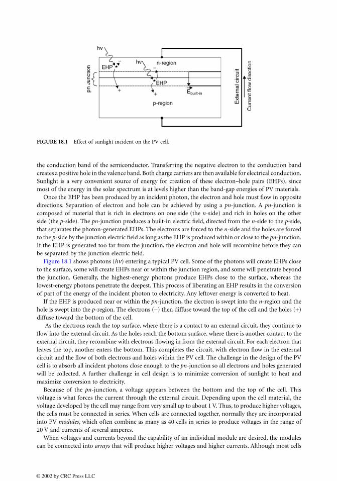
the conduction band of the semiconductor. Transferring the negative electron to the conduction bandcreates a positive hole in the valence band. Both charge carriers are then available for electrical conduction.Sunlight is a very convenient source of energy for creation of these electron–hole pairs (EHPs), sincemost of the energy in the solar spectrum is at levels higher than the band-gap energies of PV materials.
Once the EHP has been produced by an incident photon, the electron and hole must flow in oppositedirections. Separation of electron and hole can be achieved by using a pn-junction. A pn-junction iscomposed of material that is rich in electrons on one side (the n-side) and rich in holes on the otherside (the p-side). The pn-junction produces a built-in electric field, directed from the n-side to the p-side,that separates the photon-generated EHPs. The electrons are forced to the n-side and the holes are forcedto the p-side by the junction electric field as long as the EHP is produced within or close to the pn-junction.If the EHP is generated too far from the junction, the electron and hole will recombine before they canbe separated by the junction electric field.
Figure 18.1 shows photons (hν) entering a typical PV cell. Some of the photons will create EHPs closeto the surface, some will create EHPs near or within the junction region, and some will penetrate beyondthe junction. Generally, the highest-energy photons produce EHPs close to the surface, whereas thelowest-energy photons penetrate the deepest. This process of liberating an EHP results in the conversionof part of the energy of the incident photon to electricity. Any leftover energy is converted to heat.
If the EHP is produced near or within the pn-junction, the electron is swept into the n-region and thehole is swept into the p-region. The electrons (−) then diffuse toward the top of the cell and the holes (+)diffuse toward the bottom of the cell.
As the electrons reach the top surface, where there is a contact to an external circuit, they continue toflow into the external circuit. As the holes reach the bottom surface, where there is another contact to theexternal circuit, they recombine with electrons flowing in from the external circuit. For each electron thatleaves the top, another enters the bottom. This completes the circuit, with electron flow in the externalcircuit and the flow of both electrons and holes within the PV cell. The challenge in the design of the PVcell is to absorb all incident photons close enough to the pn-junction so all electrons and holes generatedwill be collected. A further challenge in cell design is to minimize conversion of sunlight to heat andmaximize conversion to electricity.
Because of the pn-junction, a voltage appears between the bottom and the top of the cell. Thisvoltage is what forces the current through the external circuit. Depending upon the cell material, thevoltage developed by the cell may range from very small up to about 1 V. Thus, to produce higher voltages,the cells must be connected in series. When cells are connected together, normally they are incorporatedinto PV modules, which often combine as many as 40 cells in series to produce voltages in the range of20 V and currents of several amperes.
When voltages and currents beyond the capability of an individual module are desired, the modulescan be connected into arrays that will produce higher voltages and higher currents. Although most cells
FIGURE 18.1 Effect of sunlight incident on the PV cell.
© 2002 by CRC Press LLC
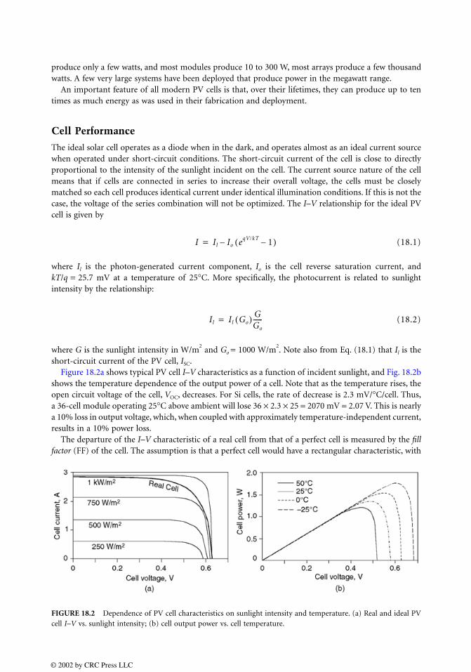
produce only a few watts, and most modules produce 10 to 300 W, most arrays produce a few thousandwatts. A few very large systems have been deployed that produce power in the megawatt range.
An important feature of all modern PV cells is that, over their lifetimes, they can produce up to tentimes as much energy as was used in their fabrication and deployment.
Cell Performance
The ideal solar cell operates as a diode when in the dark, and operates almost as an ideal current sourcewhen operated under short-circuit conditions. The short-circuit current of the cell is close to directlyproportional to the intensity of the sunlight incident on the cell. The current source nature of the cellmeans that if cells are connected in series to increase their overall voltage, the cells must be closelymatched so each cell produces identical current under identical illumination conditions. If this is not thecase, the voltage of the series combination will not be optimized. The I–V relationship for the ideal PVcell is given by
(18.1)
where Il is the photon-generated current component, Io is the cell reverse saturation current, andkT/q = 25.7 mV at a temperature of 25°C. More specifically, the photocurrent is related to sunlightintensity by the relationship:
(18.2)
where G is the sunlight intensity in W/m2 and Go = 1000 W/m
2. Note also from Eq. (18.1) that Il is the
short-circuit current of the PV cell, ISC.Figure 18.2a shows typical PV cell I–V characteristics as a function of incident sunlight, and Fig. 18.2b
shows the temperature dependence of the output power of a cell. Note that as the temperature rises, theopen circuit voltage of the cell, VOC, decreases. For Si cells, the rate of decrease is 2.3 mV/°C/cell. Thus,a 36-cell module operating 25°C above ambient will lose 36 × 2.3 × 25 = 2070 mV = 2.07 V. This is nearlya 10% loss in output voltage, which, when coupled with approximately temperature-independent current,results in a 10% power loss.
The departure of the I–V characteristic of a real cell from that of a perfect cell is measured by the fillfactor (FF) of the cell. The assumption is that a perfect cell would have a rectangular characteristic, with
FIGURE 18.2 Dependence of PV cell characteristics on sunlight intensity and temperature. (a) Real and ideal PVcell I–V vs. sunlight intensity; (b) cell output power vs. cell temperature.
I Il Io eqV/kT 1–( )–=
Il Il Go( ) GGo
------=
© 2002 by CRC Press LLC
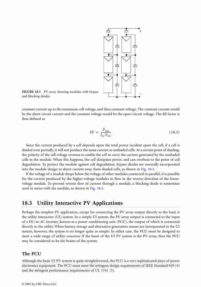
constant current up to the maximum cell voltage, and then constant voltage. The constant current wouldbe the short-circuit current and the constant voltage would be the open-circuit voltage. The fill factor isthus defined as
(18.3)
Since the current produced by a cell depends upon the total power incident upon the cell, if a cell isshaded even partially, it will not produce the same current as unshaded cells. At a certain point of shading,the polarity of the cell voltage reverses to enable the cell to carry the current generated by the unshadedcells in the module. When this happens, the cell dissipates power, and can overheat to the point of celldegradation. To protect the module against cell degradation, bypass diodes are normally incorporatedinto the module design to shunt current away from shaded cells, as shown in Fig. 18.3.
If the voltage of a module drops below the voltage of other modules connected in parallel, it is possiblefor the current produced by the higher-voltage modules to flow in the reverse direction of the lower-voltage module. To prevent reverse flow of current through a module, a blocking diode is sometimesused in series with the module, as shown in Fig. 18.3.
18.3 Utility Interactive PV Applications
Perhaps the simplest PV application, except for connecting the PV array output directly to the load, isthe utility interactive (UI) system. In a simple UI system, the PV array output is connected to the inputof a DC-to-AC inverter, known as a power conditioning unit (PCU), the output of which is connecteddirectly to the utility. When battery storage and alternative generation means are incorporated in the UIsystem, however, the system is no longer quite as simple. In either case, the PCU must be designed tomeet a wide range of utility concerns. If the heart of the UI PV system is the PV array, then the PCUmay be considered to be the brains of the system.
The PCU
Although the basic UI PV system is quite straightforward, the PCU is a very sophisticated piece of powerelectronics equipment. The PCU must meet the stringent design requirements of IEEE Standard 929 [4]and the stringent performance requirements of UL 1741 [5].
FIGURE 18.3 PV array showing modules with bypassand blocking diodes.
FFPmax
ISCVOC
----------------=
© 2002 by CRC Press LLC
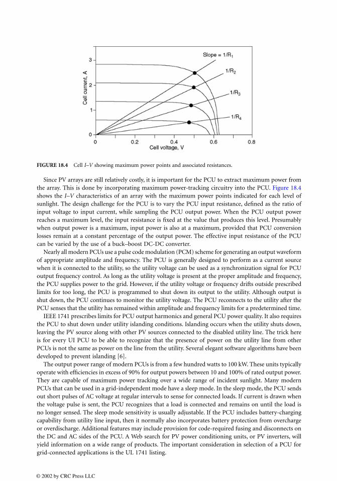
Since PV arrays are still relatively costly, it is important for the PCU to extract maximum power fromthe array. This is done by incorporating maximum power-tracking circuitry into the PCU. Figure 18.4shows the I–V characteristics of an array with the maximum power points indicated for each level ofsunlight. The design challenge for the PCU is to vary the PCU input resistance, defined as the ratio ofinput voltage to input current, while sampling the PCU output power. When the PCU output powerreaches a maximum level, the input resistance is fixed at the value that produces this level. Presumablywhen output power is a maximum, input power is also at a maximum, provided that PCU conversionlosses remain at a constant percentage of the output power. The effective input resistance of the PCUcan be varied by the use of a buck–boost DC-DC converter.
Nearly all modern PCUs use a pulse code modulation (PCM) scheme for generating an output waveformof appropriate amplitude and frequency. The PCU is generally designed to perform as a current sourcewhen it is connected to the utility, so the utility voltage can be used as a synchronization signal for PCUoutput frequency control. As long as the utility voltage is present at the proper amplitude and frequency,the PCU supplies power to the grid. However, if the utility voltage or frequency drifts outside prescribedlimits for too long, the PCU is programmed to shut down its output to the utility. Although output isshut down, the PCU continues to monitor the utility voltage. The PCU reconnects to the utility after thePCU senses that the utility has remained within amplitude and frequency limits for a predetermined time.
IEEE 1741 prescribes limits for PCU output harmonics and general PCU power quality. It also requiresthe PCU to shut down under utility islanding conditions. Islanding occurs when the utility shuts down,leaving the PV source along with other PV sources connected to the disabled utility line. The trick hereis for every UI PCU to be able to recognize that the presence of power on the utility line from otherPCUs is not the same as power on the line from the utility. Several elegant software algorithms have beendeveloped to prevent islanding [6].
The output power range of modern PCUs is from a few hundred watts to 100 kW. These units typicallyoperate with efficiencies in excess of 90% for output powers between 10 and 100% of rated output power.They are capable of maximum power tracking over a wide range of incident sunlight. Many modernPCUs that can be used in a grid-independent mode have a sleep mode. In the sleep mode, the PCU sendsout short pulses of AC voltage at regular intervals to sense for connected loads. If current is drawn whenthe voltage pulse is sent, the PCU recognizes that a load is connected and remains on until the load isno longer sensed. The sleep mode sensitivity is usually adjustable. If the PCU includes battery-chargingcapability from utility line input, then it normally also incorporates battery protection from overchargeor overdischarge. Additional features may include provision for code-required fusing and disconnects onthe DC and AC sides of the PCU. A Web search for PV power conditioning units, or PV inverters, willyield information on a wide range of products. The important consideration in selection of a PCU forgrid-connected applications is the UL 1741 listing.
FIGURE 18.4 Cell I–V showing maximum power points and associated resistances.
© 2002 by CRC Press LLC
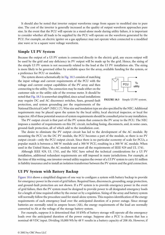
It should also be noted that inverter output waveforms range from square to modified sine to puresine. The cost of the inverter is generally increased as the quality of output waveform approaches puresine. In the event that the PCU will operate in a stand-alone mode during utility failure, it is importantto consider whether all loads to be supplied by the PCU will operate on the waveform generated by thePCU. For example, an electric igniter on a gas appliance may not operate when connected to a modifiedsine wave or to a square wave voltage waveform.
Simple UI PV System
Because the output of a UI PV system is connected directly to the electric grid, any excess output willbe used by the grid and any deficiency in PV output will be made up by the grid. Hence, the sizing ofthe simple UI PV system is not necessarily related to the load at the UI PV installation site. The sizingis more likely to be governed either by available space for the array, available funding for the system, ora preference for PCU or modules.
The system shown schematically in Fig. 18.5 consists of matchingthe input voltage and current requirements of the PCU with thevoltage and current output capabilities of the PV array and thenconnecting to the utility. The connection may be made either on thecustomer side or the utility side of the revenue meter. It should benoted that Fig. 18.5 is somewhat simplified, since actual installationsmay require DC and AC disconnect switches, fuses, ground-faultprotection, and system grounding per the requirements of theNational Electrical Code® (NEC) [7]. Wire size and insulation type are also specified by the NEC. Additionalrequirements may be placed upon the system by the local utility, local electrical inspector, or local fireinspector. All of these potential sources of system requirements should be consulted prior to any installation.
The PV output circuit is that part of the PV system that connects the PV array to the PCU. The NECimposes a number of requirements on this DC circuit, including fusing, disconnects, and, in some cases,ground-fault protection, all of which add to the installation cost.
The desire to eliminate the PV output circuit has led to the development of the AC module. Bymounting the PCU on the DC PV module, the PCU becomes a part of the module, so there is no PVoutput circuit—only the PCU output circuit. Since there is no particular economy of scale for PCUs, apopular match is between a 300 W module and a 300 W PCU, resulting in a 300 W AC module. Whenused in the United States, the AC module must meet all the requirements of IEEE 929 and UL 1741.
Although IEEE 929, UL 1741, and the NEC have solved the technical considerations for a UI PVinstallation, additional redundant requirements are still imposed in many jurisdictions. For example, atthe time of this writing, one investor-owned utility requires the owner of a UI PV system to carry $1 millionin liability insurance and to install an isolation transformer between the PV system and the grid connection.
UI PV System with Battery Backup
Figure 18.6 shows a simplified diagram of one way to configure a system with battery backup to providefor emergency power in the event of grid failure. Required fuses, disconnects, grounding, surge protection,and ground-fault protection are not shown. If a PV system is to provide emergency power in the eventof grid failure, then the PV system must be designed to provide power to all designated emergency loadsfor a length of time required either by the owner or by a regulation. Sizing of the array and battery systemwill normally follow the procedure used for stand-alone systems. This requires identification of the energyrequirements of each emergency load over the anticipated duration of a power outage. Since storagebatteries are normally rated in ampere hours (Ah), the energy requirements of the load are normallyconverted to Ah at the voltage of the storage battery system.
For example, suppose it is determined that 10 kWh of battery storage will operate all the emergencyloads over the anticipated duration of the power outage. Suppose also a PCU is chosen that has anominal 48 VDC input. Dividing 10,000 Wh by 48 V results in a battery capacity of 208 Ah. However, if
FIGURE 18.5 Simple UI PV system.
© 2002 by CRC Press LLC
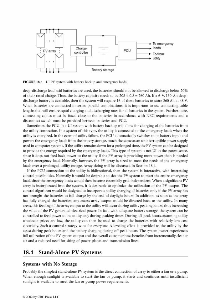
deep-discharge lead acid batteries are used, the batteries should not be allowed to discharge below 20%of their rated charge. Thus, the battery capacity needs to be 208 ÷ 0.8 = 260 Ah. If a 6-V, 130-Ah deep-discharge battery is available, then the system will require 16 of these batteries to store 260 Ah at 48 V.When batteries are connected in series–parallel combinations, it is important to use connecting cablelengths that will ensure equal charging and discharging rates for all batteries in the system. Furthermore,connecting cables must be fused close to the batteries in accordance with NEC requirements and adisconnect switch must be provided between batteries and PCU.
Sometimes the PCU in a UI system with battery backup will allow for charging of the batteries fromthe utility connection. In a system of this type, the utility is connected to the emergency loads when theutility is energized. In the event of utility failure, the PCU automatically switches to its battery input andpowers the emergency loads from the battery storage, much the same as an uninterruptible power supplyused in computer systems. If the utility remains down for a prolonged time, the PV system can be designedto provide the energy required by the emergency loads. This type of system is not UI in the purest sense,since it does not feed back power to the utility if the PV array is providing more power than is neededby the emergency load. Normally, however, the PV array is sized to meet the needs of the emergencyloads over a prolonged utility outage. Array sizing will be discussed in Section 18.4.
If the PCU connection to the utility is bidirectional, then the system is interactive, with interestingcontrol possibilities. Normally it would be desirable to size the PV system to meet the entire emergencyload, since the emergency loads would then become essentially grid independent. When a significant PVarray is incorporated into the system, it is desirable to optimize the utilization of the PV output. Thecontrol algorithm would be designed to incorporate utility charging of batteries only if the PV array hasnot brought the batteries to full charge by the end of daylight hours. In addition, as soon as the arrayhas fully charged the batteries, any excess array output would be directed back to the utility. In manyareas, this feeding of the array output to the utility will occur during utility peaking hours, thus increasingthe value of the PV-generated electrical power. In fact, with adequate battery storage, the system can becontrolled to feed power to the utility only during peaking times. During off-peak hours, assuming utilitywholesale prices are low, the utility can then be used to charge the batteries with relatively low-costelectricity. Such a control strategy wins for everyone. A leveling effect is provided to the utility by theassist during peak hours and the battery charging during off-peak hours. The system owner experiencesfull utilization of the PV system output and the overall customer base benefits from incrementally cleanerair and a reduced need for siting of power plants and transmission lines.
18.4 Stand-Alone PV Systems
Systems with No Storage
Probably the simplest stand-alone PV system is the direct connection of array to either a fan or a pump.When enough sunlight is available to start the fan or pump, it starts and continues until insufficientsunlight is available to meet the fan or pump power requirements.
FIGURE 18.6 UI PV system with battery backup and emergency loads.
© 2002 by CRC Press LLC

The next step is to incorporate some sort of power electronics into the system to provide a better matchbetween PV system output and load requirements. For example, a small amount of energy storage canassist the PV system in overcoming the starting torque of the fan or pump. A maximum power tracker(MPT), as described earlier, can ensure that the PV output is matched to the load resistance. Providingan MPT allows a system with a fixed fan or pump size to provide maximum water or airflow for a givenarray size. Without the MPT, a larger array size will be needed to achieve the same performance from thefan or pump. Sizing of such a system involves the determination of minimum operating parameters forthe pump or fan and then choosing the combination of array and MPT to meet these conditions.
Systems with Storage
If a system is to operate on cloudy days or after sundown, a means of energy storage will be required.Although exotic means such as fuel cells or hydrogen storage are possible, the most common storage meansat the time of this writing is still the lead acid storage battery. For PV energy storage applications, the deep-discharge variety of lead acid battery is used, as opposed to the automotive type that provides high currentfor short time periods. Examples of systems that require storage include lighting systems, highway infor-mation and warning signs, cathodic protection systems, refrigeration systems, communication systems, andremote dwellings. If the grid connection is eliminated, the system shown in Fig. 18.6 is representative of astand-alone system with battery storage. If the system has only DC loads, then the PCU is replaced witha discharge controller to disconnect the loads if the battery state of charge drops too low.
If the utility connection in Fig. 18.6 is replaced with an auxiliary fossil fuel or wind generator, thesystem then becomes a hybrid system, where an auxiliary power source is made available to augment thePV power. Hybrid systems are most cost-effective when the PV array must be sized to meet the demandsof low sun periods with resulting significant excess PV energy during high sun periods. For example, inFairbanks, AK, a one-axis tracking array that follows the sun from sunrise to sunset will be exposed tothe equivalent of nearly 9 h of full sun in May, but will receive no sun at all in December. An alternativepower source must then be provided for the winter months, unless no load is present.
Design of a system with storage involves determining the daily or weekly system load in Ah, determiningthe number of storage days required, determining system losses, determining the battery requirements,and determining the array requirements. The design also requires selecting appropriate charge controller,PCU or other power electronic equipment, switches, fuses, wires, and surge protectors.
The connected daily Ah load of the stand-alone system is the Ah that must be delivered to the load,including any losses in inversion of DC to AC to provide power to AC loads. Inverter losses are generallyassumed to be 10% unless specific inverter (PCU) data indicate different loss values. The corrected Ahload of a PV system is the Ah that must be supplied to the batteries to overcome battery losses and wiringlosses and still supply the connected load. Battery sizing and array sizing are based upon the corrected loadof the system, which is typically about 12% higher than the connected Ah load.
The number of storage days, also known as days of autonomy, is determined by whether the load isconsidered to be critical or noncritical. Critical loads are defined as loads that are met 99% of the timeby the PV system, whereas noncritical loads only require 95% system availability. Hence, critical loadsrequire more days of autonomy, and the days of autonomy depend upon the specific geographic location.For example, in Albuquerque, NM, a critical load requires approximately 7 days of autonomy, whereas acritical load in Seattle, WA, requires approximately 16 days of autonomy. Noncritical loads in Albuquerquerequire only 2 days of autonomy, but in Seattle require 4 days of autonomy.
System losses can normally be considered to be 10% for battery charging and discharging losses, and2 to 3% for wiring losses. Battery losses are due to conversion of electrical energy to heat energy whilecharging or discharging the batteries. In addition, the PV array is generally derated to account for elevatedarray temperatures and degradation of the array from dust and dirt.
Once the corrected load is known, battery sizing can be accomplished by using
(18.4)AhAhday--------
daysDTDch disch( )--------------------------------
=
© 2002 by CRC Press LLC
where Ah is the required battery capacity, Ah/day is the system corrected load, days is the number ofdays of autonomy required, and DT is a temperature correction factor that varies linearly from unity at80°F to 0.72 at 32°F. Dch is a discharge correction factor that is unity as long as the batteries dischargeat less than the rated discharge rate. For faster discharge rates lasting more than 10 min, Dch is the ratioof the rated discharge rate to the actual discharge rate. Finally, (disch) is the design depth of discharge,normally in the range of 0.5 to 0.8, with 0.8 representing the loss of 80% of rated charge.
Array sizing is also based on the corrected load of the system, since the array must supply the correctedload to the batteries at the selected battery voltage. Array sizing also depends upon any degradation ofarray output and upon available sunlight. In areas where the array is likely to become dusty or where itis likely to operate more than a few degrees above 25°C, the degradation factor may be as high as 15 to 20%.Sunlight is measured in terms of peak sun hours (PSH). The PSH for a location on a particular day isdetermined by measuring the daily kWh/m
2 incident upon the array. Monthly expected PSH are tabulated
for many locations, based upon measurements over periods of 20 years or more. In addition to the PSH,standard deviations are also available for use when worst-case estimates need to be made. The FloridaSolar Energy Center maintains a Web site with links to a wide range of PV information, including sunlightintensity data [8]. When the corrected load, system voltage, degradation factor, and PSH informationare available, the array size can be determined from
(18.5)
where I is the rated array current, Ah is the system corrected load, PSHmin is the minimum PSH for thePV system site, and η is the array degradation factor. Note that as PSH decreases for the winter months,η increases as the array temperature decreases. It is thus useful to estimate PSH and η for winter andsummer and then use the smaller of the two products in Eq. (18.5). Modules are then connected in seriesto achieve the system design voltage and in parallel to obtain the system design current. System voltagestypically are selected in multiples of 12, while system currents depend upon the specific loads.
The PSH for a PV array depends upon the month of the year as well as the tilt of the array. The PSHalso depends upon whether the array is a fixed array or a single- or double-axis tracking array. The PSHtables typically list the available PSH for several different tilt angles. For best annual performance, theoptimal tilt of a fixed PV array is approximately latitude −10°. If an array is to supply different loads fordifferent seasons, then the array may be tilted to optimize seasonal performance.
After the batteries and array have been selected, the system power electronic components are selected.The charge controller is an important part of the system and can range from relatively simple design torelatively complex design. A simple controller monitors battery voltage and diverts the array currentoutput when the battery voltage reaches the manufacturer’s specified full-charge voltage. A better con-troller also monitors when the batteries are at the design discharge voltage and disconnects the batteriesfrom the load at this point. An even better controller monitors the battery temperature and compensatesthe array disconnect voltage and the load disconnect voltage for temperature. A further controllerimprovement employs maximum power tracking to ensure maximum transfer of charge from array tobatteries and provides for diversion of the PV output to an alternate load after the batteries are fullycharged. Some controllers incorporate most of the features listed, but must be set either for charge controlor discharge control. In a stand-alone system with AC loads, the PCU will normally incorporate thedischarge protection feature. If no AC loads are present, a separate discharge controller may be needed.
The internal resistance of a battery system introduces a hysteresis effect into the charge and dischargeprocess. When the batteries are charging, the terminal voltage becomes greater than the cell voltage as aresult of the additional voltage drop across the internal battery resistance between the terminals and thecells. Hence, if the terminal voltage is sensed, it will drop when the charger is disconnected. This maycause the charger to be reconnected, if the terminal voltage drops below the full-charge value. Becauseof the hysteresis effect, charge controllers normally are designed to provide a three-stage charging process.Initially, the batteries are charged at constant current. When the batteries reach a predetermined terminal
IAh
PSHmin h×---------------------------=
© 2002 by CRC Press LLC

voltage, they are charged at constant voltage until the current drops to a prescribed level. At this point,the charge controller voltage decreases to complete the charging process at a lower current level.
During discharge, the battery terminal voltage is lower than the battery cell voltage, since the currentthrough the battery internal resistance is now in the opposite direction. The discharge control must thusincorporate a means of avoiding oscillation on and off when the battery terminal voltage indicates thatthe battery is approaching minimum allowable charge.
The PCU in a stand-alone system does not need to comply with IEEE 929 or UL 1741. It thus canrange from a relatively simple square wave inverter to a more-sophisticated, microprocessor-controlledPCM inverter that employs amplitude and/or frequency control of the output waveform as well as manyother features described earlier in this chapter.
References
1. Markvart, T., Ed., Solar Electricity, John Wiley & Sons, Chichester, U.K., 1994. 2. Messenger, R. A. and Ventre, J., Photovoltaic Systems Engineering, CRC Press, Boca Raton, FL, 1999.3. Stand-Alone Photovoltaic Systems: A Handbook of Recommended Design Practices, Sandia National
Laboratories, Albuquerque, NM, 1995.4. ANSI/IEEE P929, IEEE Recommended Practice for Utility Interface of Residential and Intermediate
Photovoltaic (PV) Systems, IEEE Standards Coordinating Committee 21, Photovoltaics, Draft 10,February 1999.
5. UL 1741: 1999, Standard for Static Inverters and Charge Controllers for Use in Photovoltaic PowerSystems, Underwriters Laboratories, Inc., Northbrook, IL, May 1999.
6. Kern, G. A., Bonn, R. H., Ginn, J., and Gonzalez, S., Results of Sandia National Laboratories grid-tied inverter testing, in Proc. 2nd World Conference and Exhibition on PV Solar Energy Conversion,Vienna, Austria, July, 1998.
7. NFPA 70 National Electrical Code, 1999 Edition, National Fire Protection Association, Quincy, MA,1998.
8. http://alpha.fsec.ucf.edu/~pv (Florida Solar Energy Center PV home page).
© 2002 by CRC Press LLC
19Flexible, Reliable, and
Intelligent ElectricalEnergy Delivery
Systems
19.1 Introduction19.2 The Concept of FRIENDS
What Is FRIENDS? • Quality Control Centers • Intelligent Function of FRIENDS
19.3 Development of FRIENDS19.4 The Advanced Power Electronic
Technologies within QCCsDistribution Static Compensator • Dynamic Voltage Restorer • Solid-State Breaker
19.5 Significance of FRIENDS19.6 Realization of FRIENDS19.7 Conclusions
19.1 Introduction
There have been considerable changes in today’s power systems in recent years, due, in large part, to theemergence of competition and deregulation in power industries. The goal of deregulation is to providethe customer with reduced costs. The global competition between utilities leads to utility cost-cutting,downsizing, and reducing maintenance on both transmission and distribution systems. Power systemsthat are hierarchically integrated are separated such that tasks normally carried out within traditionalorganizations have been open to competition whenever practical and profitable. This process, which iscalled “unbundling,” consists of unbundling of vertically integrated utilities, unbundling of functionswithin a corporation, and service unbundling. As a consequence, the common structure in the deregulatedpower industry is the separation of the generation, transmission, and distribution business into separateentities. There is, however, a possible drop in service quality as a result of deregulation. Additionally,installation and penetration of distributed generators (DGs) and distributed energy storage systems(DESSs), allocated in the demand-side of power systems, have been increased. Unexpected power qualityproblems may occur, because these distributed facilities are operated independently and are uncommittedto the operating situation of power systems.
Power quality issues have become more important in the face of this open competition. In recent yearsthere has been an increase in the number of system loads and controls that are sensitive to power quality,as well as an increase in the number of system loads that are themselves a source of poor power quality
Alexander Domijan, Jr.University of Florida
Zhidong SongUniversity of Florida
© 2002 by CRC Press LLC

(such as harmonics caused by static drives). Loads such as computers, process controls, and communi-cations equipment are more sensitive to power quality variations due to frequent system disturbancesthan is equipment applied in the past. On the other hand, there has been continuing growth in theapplication of power electronics devices, both to improve the overall power system efficiency and tofacilitate controls. This is resulting in increasing power quality problems on power systems, for theseloads themselves are major causes of the degradation of power quality. Yet awareness of power qualityissues is increased by the end users who need a high quality of power for their equipment and arebecoming better informed about such issues as voltage sags, swells, surges, harmonic distortions, inter-ruptions, outages, undervoltages, overvoltages, electrical noise, frequency deviations, impulses, transients,and notches. They need to understand how the disturbances will affect sensitive loads and thereforedevelop appropriate specifications, or install appropriate power conditioning systems [1]. Harmonics,for example, can result in equipment heating and voltage stress, communication interference, and controlmalfunctions. Voltage sags of only a few cycles can cause tripping of drives, loss of computer data, orerrors. As a matter of fact, utilities are being challenged to improve the quality of power delivered byevery possible means.
Power quality, therefore, is the benchmark by which we may judge the success of our problem solution.Reliable and secure power service needs to be made available to customers. Customers, who need a highquality of power for their equipment and are becoming better informed about power quality issues,provide the principal motivation for the utility industry with unbundled services and greater reliance oncompetitive forces. They, then, would be free to select their desired level of power quality. There isopportunity for enhanced value of service through greater choice among customized and competitiveservices. Yet the utility industry itself, under the threat of competition, on the other hand, is likely to beforced to offer a variety of valued-added unbundled services and prices to customers to increase customersatisfaction. It may be assumed that the customer or market will play the lead over that of the energysupplier. Information-based electric suppliers, both with and without generation sources, will be able toattract large portions of market share from the traditional suppliers. Therefore, electric utilities must beprepared to develop a strategic methodology both to satisfy their existing customer base and to captureadditional customers as competition unfolds. One way to accomplish these goals is via the businessstrategy of providing unbundled or differentiated services/products. The rapid advance in technologiessuch as power electronics, small-scale energy generators and storage, and computer control has madefeasible distributed systems and the unbundling of power services.
Advanced technologies including power electronics, together with new coordination mechanisms,should be taken into account to ensure the quality of an unbundling service on reasonable levels. Newsystem configurations and control schemes are desired under the above situations. Many technicalproblems need to be solved. The new concept of Flexible, Reliable, and Intelligent Electrical EnergyDelivery Systems (FRIENDS) is such a methodology for electric power infrastructure development andinformation management systems to realize such an unbundled power quality service.
19.2 The Concept of FRIENDS
What Is FRIENDS?
Similar to the early days of the electric utility industry, a product, unbundled power quality services, isneeded first to create a market. The unbundling of power quality services, defined as permitting severallevels of power quality at a differentiated cost, is a business concept that achieves its potential in thepresence of technologies that can provide specific customers with more than one level of power quality.Ideally, such technologies would provide a range of user choices, of readily calculable economic value,that could be reoptimized as the needs of the user evolve. This then allows expansion of the FRIENDSinfrastructure (from revenues generated by the first products introduced) to reach a larger market forservices rendered. This process is not likely to be implemented suddenly. Rather, a systematic approach,[2] as illustrated in Fig. 19.1, is the more likely scenario for this century. The enabling products are those
© 2002 by CRC Press LLC
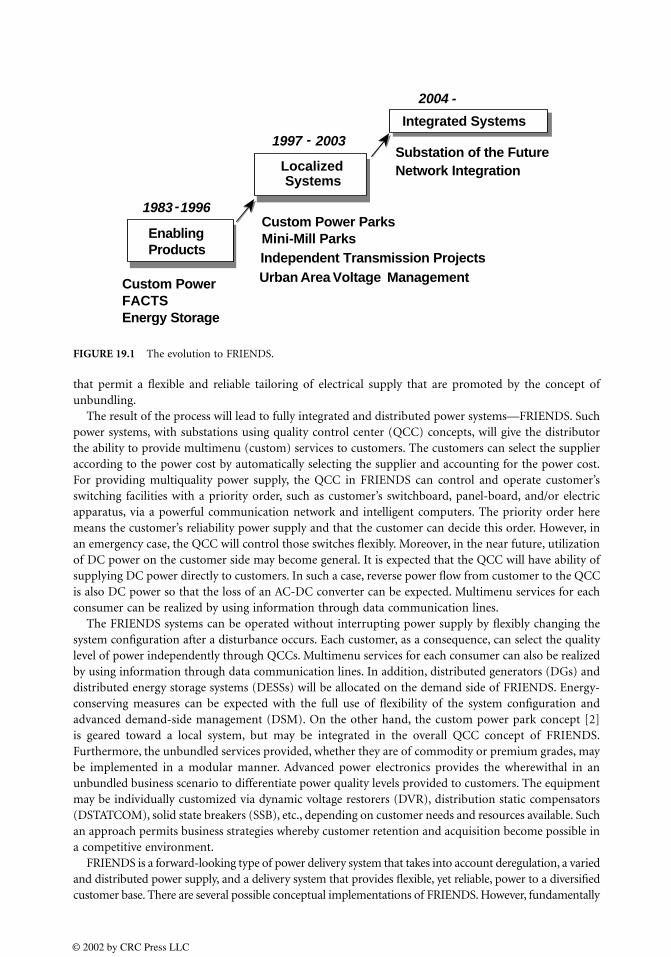
that permit a flexible and reliable tailoring of electrical supply that are promoted by the concept ofunbundling.
The result of the process will lead to fully integrated and distributed power systems—FRIENDS. Suchpower systems, with substations using quality control center (QCC) concepts, will give the distributorthe ability to provide multimenu (custom) services to customers. The customers can select the supplieraccording to the power cost by automatically selecting the supplier and accounting for the power cost.For providing multiquality power supply, the QCC in FRIENDS can control and operate customer’sswitching facilities with a priority order, such as customer’s switchboard, panel-board, and/or electricapparatus, via a powerful communication network and intelligent computers. The priority order heremeans the customer’s reliability power supply and that the customer can decide this order. However, inan emergency case, the QCC will control those switches flexibly. Moreover, in the near future, utilizationof DC power on the customer side may become general. It is expected that the QCC will have ability ofsupplying DC power directly to customers. In such a case, reverse power flow from customer to the QCCis also DC power so that the loss of an AC-DC converter can be expected. Multimenu services for eachconsumer can be realized by using information through data communication lines.
The FRIENDS systems can be operated without interrupting power supply by flexibly changing thesystem configuration after a disturbance occurs. Each customer, as a consequence, can select the qualitylevel of power independently through QCCs. Multimenu services for each consumer can also be realizedby using information through data communication lines. In addition, distributed generators (DGs) anddistributed energy storage systems (DESSs) will be allocated on the demand side of FRIENDS. Energy-conserving measures can be expected with the full use of flexibility of the system configuration andadvanced demand-side management (DSM). On the other hand, the custom power park concept [2]is geared toward a local system, but may be integrated in the overall QCC concept of FRIENDS.Furthermore, the unbundled services provided, whether they are of commodity or premium grades, maybe implemented in a modular manner. Advanced power electronics provides the wherewithal in anunbundled business scenario to differentiate power quality levels provided to customers. The equipmentmay be individually customized via dynamic voltage restorers (DVR), distribution static compensators(DSTATCOM), solid state breakers (SSB), etc., depending on customer needs and resources available. Suchan approach permits business strategies whereby customer retention and acquisition become possible ina competitive environment.
FRIENDS is a forward-looking type of power delivery system that takes into account deregulation, a variedand distributed power supply, and a delivery system that provides flexible, yet reliable, power to a diversifiedcustomer base. There are several possible conceptual implementations of FRIENDS. However, fundamentally
FIGURE 19.1 The evolution to FRIENDS.
Integrated SystemsIntegrated Systems
Localized Systems
Enabling Products
Enabling Products
Substation of the FutureNetwork Integration
Custom Power ParksMini-Mill ParksIndependent Transmission ProjectsUrban Area Voltage ManagementCustom Power
FACTSEnergy Storage
1983 -1996
1997 - 2003
2004 -
© 2002 by CRC Press LLC

the network is an integrated system with the ability to provide flexibility in reconfiguration and reliabilityso that uninterrupted service is obtained. To implement such a system requires advanced power electronictechnologies to create the desired conditioned power and command-and-control technologies.
From the viewpoint of consumers, the characteristic of FRIENDS can be summarized as multiplemenu service, which may be classified into three types: multiple rate service, multiple quality service,and multiple supplier service. Specifically, FRIENDS is directed to obtain the following technical features:
• Flexibility in reconfiguration of a power system
• Reliability of power supply
• Multimenu services to allow customers to select the type of power provided and other servicesoffered by the electric utility
• Revenue-enhancement techniques
• Load leveling and energy conservation
• Enhancement of information services (utility/customer, and utility/utility)
• Effective demand-side management
• Flexibility in incorporating dispersed generation
• New automatic generation control methodologies
• Voltage regulation functions
• Fault current-limiting functions
• Prevention of sags, swells, and harmonics
• Instrumentation and revenue metering
In brief, the purpose of FRIENDS is to develop a desirable structure for future power delivery systems,where dispersed energy storage systems and dispersed generators are installed near the demand side, andto develop reliable and energy-conserving operation strategies of power systems, taking into account theways of enhancing service to customers through intelligent functions. It will be necessary for the powerindustry to create technical product differentiation that provides for the effective unbundling of powerquality services, of readily calculable value, as the needs of the customer evolve [2].
Quality Control Centers
FRIENDS can realize the most efficient use of the flow of electric energy generated by remote generators,dispersed generators, and dispersed storage devices in electric power networks. One of the most importantfeatures of FRIENDS is that new power improvement facilities referred to as quality control centers (QCCs)are installed very closely to the customers. A desirable operating algorithm of DGs and DESSs in QCCs havebeen investigated and the capacity required for the multiquality power supply have been evaluated [3–9].QCCs are developed to cope with providing flexible services to customers in an uncertain electric utilitybusiness in near future delivery systems, with which multimenu electrical power quality services are realizedin FRIENDS. A QCC is much like a switching facility with the capability to change flexibly the systemconfiguration depending on the system states. The QCCs play a vital role in the operation of FRIENDS, such as:
• Flexible change in system configuration
• Multiple menu services for customers (unbundled services)
• Information management (information processing and data exchange centers)
• Monitoring and controlling power flow by interchange of information between QCCs so that thesystem can operate in the most effective and economical way
A QCC can be supplied with electrical power from several distribution substations through severalpower lines to enhance the supply reliability as shown in Fig. 19.2. It may cover a wide area or may belocal and located at a section of the current distribution system, an underground floor of a large building,inside the area of a factory, and so forth, depending on its role. In a QCC, it is expected that electric
© 2002 by CRC Press LLC
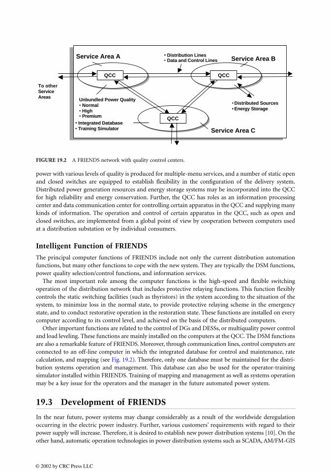
power with various levels of quality is produced for multiple-menu services, and a number of static openand closed switches are equipped to establish flexibility in the configuration of the delivery system.Distributed power generation resources and energy storage systems may be incorporated into the QCCfor high reliability and energy conservation. Further, the QCC has roles as an information processingcenter and data communication center for controlling certain apparatus in the QCC and supplying manykinds of information. The operation and control of certain apparatus in the QCC, such as open andclosed switches, are implemented from a global point of view by cooperation between computers usedat a distribution substation or by individual consumers.
Intelligent Function of FRIENDS
The principal computer functions of FRIENDS include not only the current distribution automationfunctions, but many other functions to cope with the new system. They are typically the DSM functions,power quality selection/control functions, and information services.
The most important role among the computer functions is the high-speed and flexible switchingoperation of the distribution network that includes protective relaying functions. This function flexiblycontrols the static switching facilities (such as thyristors) in the system according to the situation of thesystem, to minimize loss in the normal state, to provide protective relaying scheme in the emergencystate, and to conduct restorative operation in the restoration state. These functions are installed on everycomputer according to its control level, and achieved on the basis of the distributed computers.
Other important functions are related to the control of DGs and DESSs, or multiquality power controland load leveling. These functions are mainly installed on the computers at the QCC. The DSM functionsare also a remarkable feature of FRIENDS. Moreover, through communication lines, control computers areconnected to an off-line computer in which the integrated database for control and maintenance, ratecalculation, and mapping (see Fig. 19.2). Therefore, only one database must be maintained for the distri-bution systems operation and management. This database can also be used for the operator-trainingsimulator installed within FRIENDS. Training of mapping and management as well as systems operationmay be a key issue for the operators and the manager in the future automated power system.
19.3 Development of FRIENDS
In the near future, power systems may change considerably as a result of the worldwide deregulationoccurring in the electric power industry. Further, various customers’ requirements with regard to theirpower supply will increase. Therefore, it is desired to establish new power distribution systems [10]. On theother hand, automatic operation technologies in power distribution systems such as SCADA, AM/FM-GIS
FIGURE 19.2 A FRIENDS network with quality control centers.
QCC QCC
QCC
Service Area C
Service Area BService Area A
To other ServiceAreas Unbundled Power Quality
NormalHighPremium
Distributed SourcesEnergy Storage
Distribution LinesData and Control Lines
Integrated DatabaseTraining Simulator
© 2002 by CRC Press LLC

(Automatic Mapping/Facility Management Geographic Information Systems) have been developing rap-idly. Meanwhile, power electronic technologies, communication technologies, DSM technologies, etc.have also been developing. Some DGs and energy storage systems have been installed in distributionsystems. The complexity of the existing systems as well as the specific quality requirements of eachcustomer are expected to increase, and will consequently require more advanced electric power deliverysystems and advanced technologies. Therefore, it is possible to build new distribution systems that havemany excellent functions with these new technologies.
The advantages of FRIENDS are increasingly apparent by progress made via international collaborationin recent years. They are as follows: multiquality electric power, multimenu services and rate informationto customers, energy conservation effect with the full use of flexibility of the system configuration andadvanced DSM, and powerful intelligent communication networks along with QCCs. So far, research inthe following aspects of this field has attracted much attention:
• Optimal FRIENDS configuration for reliable power supply
• Concepts and configurations of QCCs for unbundled power quality services
• Optimal allocation of DGs
• Autonomous decentralized power distribution system (ADPDS)
• Utility and customer interface
It is necessary to develop an optimal configuration of FRIENDS from the viewpoint of power supplyreliability, to realize the unbundled power quality services through DGs and DESSs. Network connectionof FRIENDS must be flexibly changed to minimize distribution loss in a normal state, and to supplypower without interruption to customers by utilizing DGs and DESSs in a fault state, through ON/OFFstatus of solid-state transfer switches (SSTS). To solve the network configuration problem in FRIENDS,from the viewpoint of power supply reliability, an effort has been made to determine power lines andDG installations, to minimize total installation cost under constraints of the maximum capacity of DGs,line current capacity, and uninterrupted power supply. Special algorithms have been employed to solvethis problem and numerical results have been obtained [3–9]. It is expected that system configurationscan be changed flexibly, to minimize distribution losses in normal states, to restore the system swiftly inan emergency state, and to repair facilities without power interruption in a maintenance state.
A QCC is a new facility that can improve the quality of power according to customers’ requests andprovide multiquality power to customers. A QCC may be connected to multiple power lines and can besupplied with commodity quality power from several substations. The connection of many QCCs willlead to the development of a new type of high-voltage power distribution network such that QCCs canprovide power with various qualities to customers in a multimenu manner. To realize FRIENDS, detailedinterior structures of QCCs for accomplishing its functions and algorithms for optimal selection of powerquality and power provider are needed. The problems for development of a structure of QCCs are mainlyfocused on (1) a circuit configuration that makes it possible to deliver electric power with different powerquality levels and (2) the control of the static switches that are the most fundamental components of a QCC.In general, QCCs will take various kinds of interior structures according to the features of customersconnected to the QCC, conditions in the neighborhood of the QCC, location of the QCC, and installationcost of the QCC, and so on. Progress has been made on development of concepts and physical configu-rations of the QCC. The configuration of a QCC, which will be located between distribution substationsand loads, has been investigated and a prototype model of generating end-use power demand proposed[11, 12]. This model can simulate the activity of a customer and the usage patterns of energy usingappliances in the household. Three structures for industrial, business, and commercial, and residentialareas have been proposed [13, 14], where the control scheme of solid-state switches used for changingnetwork configuration and cutting off a line when abnormal voltage occurs. Further, the initial structuraldesign of a QCC has been proposed, and the interior structures of the QCC in the scheme of FRIENDS,together with qualitative explanations for various characteristics of the proposed structures, have beenprovided [15–21]. Two types of QCC models that can execute unbundled power quality services to
© 2002 by CRC Press LLC

customers, along with simulation of transient behavior of the proposed model, have been investigated.Uninterruptible power supply (UPS) system, DGs, and solid-state breakers (SSB) can be incorporatedinto the proposed QCC models. It is expected in a QCC that electric power with various levels of qualityis produced by using various types of equipment, e.g., UPS, DVR, SVC, AF (active filter), AVR (automaticvoltage regulator), FCL (fault current limiter), etc., with intelligent features. A number of solid-stateopen/close switches, DGs, and DESSs are also important facilities for realizing many of the functions tobe incorporated within a QCC. Small consumers, who are usually considered as captured consumers andcannot select their suppliers, may enjoy the multiple supplier service through the service of QCCs. Thisservice will undoubtedly encourage competition in the electric power market. In addition, a QCC canalso be considered a virtual consumer. It may choose the supplier to minimize the electricity cost.
ADPDS has been introduced as a concept of FRIENDS [22]. The major purpose in this area is to developa method to find the realizable configuration and operation of ADPDS from a viewpoint of power qualityand supply reliability under global deregulation and competition, such that the unbundled power qualityservices can be applied to traditional power distribution systems. In this concept, among many kinds ofpower qualities, power interruption or power supply reliability is the most important function of unbun-dled power quality services. A concept for real-time voltage regulation and a modeling method fordistribution systems integrated with DGs have been recently developed [23]. It is expected that this modelingmethod could be widely applied to design and operation of distribution systems with many DGs.
The distribution system envisioned by FRIENDS will need to be able to operate with an array of lines,QCCs, DGs, and storage elements—all digitally controlled so that resources are allocated flexibly, yetreliably. Similarly, the transmission system must also be controlled effectively to handle the transactionincreases expected. Both on the distribution and transmission sides this may be accomplished via amultilevel hierarchical control structure [24–26], which incorporates FRIENDS, FACTS, Custom Power,and wide-area communication technologies. Both a power supply and delivery technology (one that isflexible, robust, and efficient) are required to sustain the expected use of energy. FRIENDS is the key forsuch a successful delivery system. However, FRIENDS technology must be implemented on a value-addedbasis; otherwise, one risks returns on investment not well optimized with respect to the cost of capital.What is needed is a sensible roadmap of value-added innovation that fits within anticipated optionsavailable to customers. Research on other areas such as security constrained power planning and oper-ations in competitive market [27], DSM, and computer technologies in FRIENDS [28] are under way.
19.4 The Advanced Power Electronic Technologieswithin QCCs
Power quality for unbundled power quality services may be considered on three levels—normal quality,high quality, and premium quality—depending on demand characteristics of customers. In the conceptof FRIENDS, QCCs have transfer switches to reduce distribution losses, voltage sags, swells, flickers,interruptions, three-phase voltage unbalance, and voltage harmonics, by using advanced power electron-ics devices such as DSTATCOM, DVR, UPS, and SSB or SSTS.
Distribution Static Compensator
As a fast, flexible, and effective power quality mitigation tool, DTSATCOM is designed to protect theupstream system from “dirty” loads, surges, or harmonics caused by other users on the distributionsystem. The use of DSTATCOM devices (whose capabilities may include active filtering, reactive powersupply, and flicker correction) is becoming quite attractive for customers and distributors, partly becauseof its direct connection to the network (just as any other load element) and mainly because the samepower electronics configuration can be used, modifying the control structure, to provide the differentservices. The parallel-connected DSTATCOM with the load provides dynamic, subcycle voltage supportand regulation of reactive power flow. It is capable of generating continuously adjustable reactive or
© 2002 by CRC Press LLC
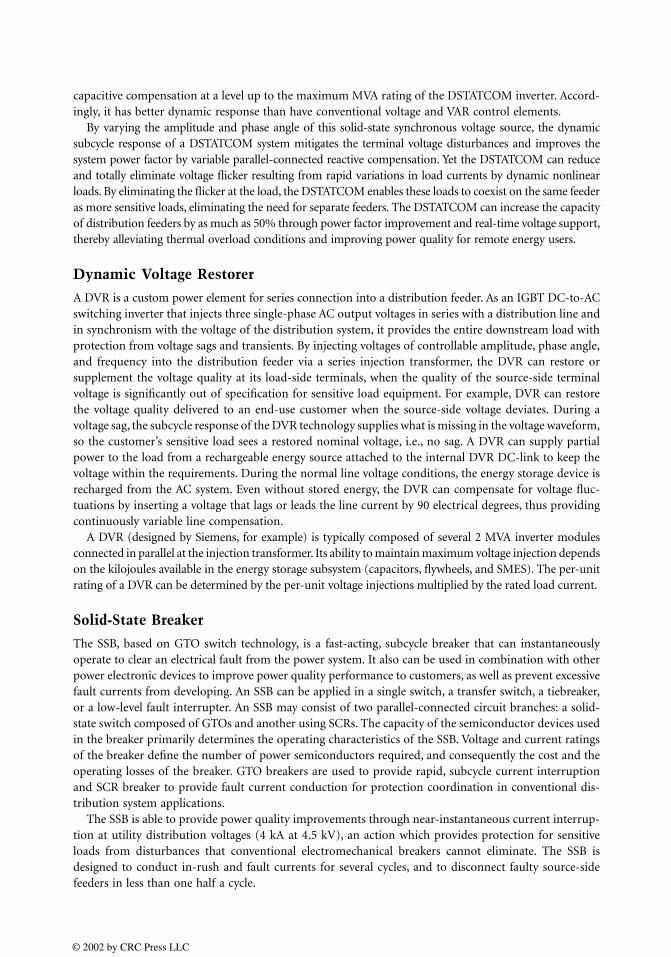
capacitive compensation at a level up to the maximum MVA rating of the DSTATCOM inverter. Accord-ingly, it has better dynamic response than have conventional voltage and VAR control elements.
By varying the amplitude and phase angle of this solid-state synchronous voltage source, the dynamicsubcycle response of a DSTATCOM system mitigates the terminal voltage disturbances and improves thesystem power factor by variable parallel-connected reactive compensation. Yet the DSTATCOM can reduceand totally eliminate voltage flicker resulting from rapid variations in load currents by dynamic nonlinearloads. By eliminating the flicker at the load, the DSTATCOM enables these loads to coexist on the same feederas more sensitive loads, eliminating the need for separate feeders. The DSTATCOM can increase the capacityof distribution feeders by as much as 50% through power factor improvement and real-time voltage support,thereby alleviating thermal overload conditions and improving power quality for remote energy users.
Dynamic Voltage Restorer
A DVR is a custom power element for series connection into a distribution feeder. As an IGBT DC-to-ACswitching inverter that injects three single-phase AC output voltages in series with a distribution line andin synchronism with the voltage of the distribution system, it provides the entire downstream load withprotection from voltage sags and transients. By injecting voltages of controllable amplitude, phase angle,and frequency into the distribution feeder via a series injection transformer, the DVR can restore orsupplement the voltage quality at its load-side terminals, when the quality of the source-side terminalvoltage is significantly out of specification for sensitive load equipment. For example, DVR can restorethe voltage quality delivered to an end-use customer when the source-side voltage deviates. During avoltage sag, the subcycle response of the DVR technology supplies what is missing in the voltage waveform,so the customer’s sensitive load sees a restored nominal voltage, i.e., no sag. A DVR can supply partialpower to the load from a rechargeable energy source attached to the internal DVR DC-link to keep thevoltage within the requirements. During the normal line voltage conditions, the energy storage device isrecharged from the AC system. Even without stored energy, the DVR can compensate for voltage fluc-tuations by inserting a voltage that lags or leads the line current by 90 electrical degrees, thus providingcontinuously variable line compensation.
A DVR (designed by Siemens, for example) is typically composed of several 2 MVA inverter modulesconnected in parallel at the injection transformer. Its ability to maintain maximum voltage injection dependson the kilojoules available in the energy storage subsystem (capacitors, flywheels, and SMES). The per-unitrating of a DVR can be determined by the per-unit voltage injections multiplied by the rated load current.
Solid-State Breaker
The SSB, based on GTO switch technology, is a fast-acting, subcycle breaker that can instantaneouslyoperate to clear an electrical fault from the power system. It also can be used in combination with otherpower electronic devices to improve power quality performance to customers, as well as prevent excessivefault currents from developing. An SSB can be applied in a single switch, a transfer switch, a tiebreaker,or a low-level fault interrupter. An SSB may consist of two parallel-connected circuit branches: a solid-state switch composed of GTOs and another using SCRs. The capacity of the semiconductor devices usedin the breaker primarily determines the operating characteristics of the SSB. Voltage and current ratingsof the breaker define the number of power semiconductors required, and consequently the cost and theoperating losses of the breaker. GTO breakers are used to provide rapid, subcycle current interruptionand SCR breaker to provide fault current conduction for protection coordination in conventional dis-tribution system applications.
The SSB is able to provide power quality improvements through near-instantaneous current interrup-tion at utility distribution voltages (4 kA at 4.5 kV), an action which provides protection for sensitiveloads from disturbances that conventional electromechanical breakers cannot eliminate. The SSB isdesigned to conduct in-rush and fault currents for several cycles, and to disconnect faulty source-sidefeeders in less than one half a cycle.
© 2002 by CRC Press LLC

A high-voltage SSTS can provide nearly uninterruptible power to critical distribution-served customerswho have two independent power sources. Fast-acting solid-state switches can rapidly transfer sensitiveloads from a normal or preferred supply that experiences a disturbance to an alternate or backup supplysuch as another utility primary distribution feeder or a standby power supply operated from an integralenergy storage system.
19.5 Significance of FRIENDS
FRIENDS will give consumers the ability to take advantage of multiple menu services, and utilitiesthe ability to provide flexible, reliable, and intelligent electricity services. Since consumers are givena choice with a multiple menu service, they may have greater influence on the overall system operations.The necessary condition for the existence of FRIENDS is consumer satisfaction and improved oper-ations for the utility. Because of deregulation and competition, it becomes important to providereliability and tailored services and its realization will make it economically possible to create thesystem. From this standpoint, the reliability of the high-voltage side, such as the generation and/ortransmission systems, of power networks can be less important, and the investment in it may bereduced. Therefore, a part of the investment on the high-voltage side may be diverted to the distri-bution side without a change in the total investment. However, implementation costs for QCCs willbe high because of the SSBs in its configuration. More cost reduction is necessary to make the conceptof FRIENDS realizable. FRIENDS will be developed through several items, the important of whichare (1) powerful intelligent communication networks; (2) QCCs; and (3) advanced power qualityenhancement systems. These items are interrelated and may be enhanced if considered together. TheQCC will also have dispersed generation and storage in its configuration to achieve load leveling andto supply uninterrupted power to the loads. The QCC will change the system configuration flexiblydepending on the system states, data of which are exchanged through intelligent communicationnetworks.
As mentioned in previous sections, FRIENDS integrates a number of research concepts that have beendeveloped individually, by adding more reliable and flexible functions. Distributed generation resourcesand energy storage systems, demand-side control, advanced power electronics technologies, and distrib-uted intelligent facilities can be combined into FRIENDS systems. Generally, a FRIENDS system withQCCs will play an important role in the following ways (Fig. 19.3).
Flexibility in reconfiguration of the system. With solid-state switches in a properly used QCC, thedistribution system configuration can be frequently changed according to the state and load patterns ofthe system to reduce distribution losses and load leveling and to avoid power interruption. QCCs maypermit a reverse flow of power and have the ability to bypass selected QCCs. Power electronics switches,together with computerized relaying schemes, will be utilized to make switching operations much easierand more flexible.
Reliability in power supply. In principle, power interruption never occurs in FRIENDS. To realize anuninterrupted power supply, DESS and DGs installed at the demand side are fully used under the controlof the QCC, providing flexibility in reconfiguration. A computer installed at the QCC has functionsrelated to the control of DESS and DGs, multiquality power control, and load leveling. With considerationof power interchange between QCCs, an effective operational scheme of DESSs and DGs can be attained.It is found that there might be a trade-off between the system configuration and the capacity of DESSsand DGs.
Multimenu service for customers. A QCC produces multiquality power by using DESSs and DGs. Thecustomers can select the supplier according to the power cost by automatically selecting the supplier andaccounting for the cost of energy. For providing a multiquality power supply, the QCC can control andoperate customer’s switching facilities flexibly with a priority order decided by the customer’s powersupply reliability, such as a customer’s switchboard, panel-board, and/or electric apparatus, via a powerfulcommunication network and intelligent computers.
© 2002 by CRC Press LLC
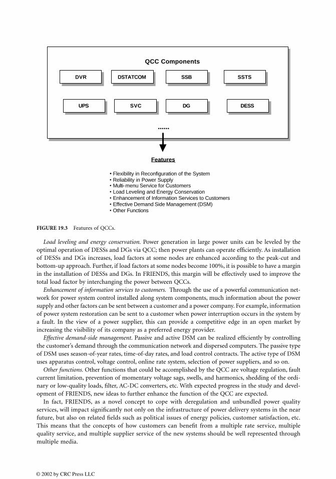
Load leveling and energy conservation. Power generation in large power units can be leveled by theoptimal operation of DESSs and DGs via QCC; then power plants can operate efficiently. As installationof DESSs and DGs increases, load factors at some nodes are enhanced according to the peak-cut andbottom-up approach. Further, if load factors at some nodes become 100%, it is possible to have a marginin the installation of DESSs and DGs. In FRIENDS, this margin will be effectively used to improve thetotal load factor by interchanging the power between QCCs.
Enhancement of information services to customers. Through the use of a powerful communication net-work for power system control installed along system components, much information about the powersupply and other factors can be sent between a customer and a power company. For example, informationof power system restoration can be sent to a customer when power interruption occurs in the system bya fault. In the view of a power supplier, this can provide a competitive edge in an open market byincreasing the visibility of its company as a preferred energy provider.
Effective demand-side management. Passive and active DSM can be realized efficiently by controllingthe customer’s demand through the communication network and dispersed computers. The passive typeof DSM uses season-of-year rates, time-of-day rates, and load control contracts. The active type of DSMuses apparatus control, voltage control, online rate system, selection of power suppliers, and so on.
Other functions. Other functions that could be accomplished by the QCC are voltage regulation, faultcurrent limitation, prevention of momentary voltage sags, swells, and harmonics, shedding of the ordi-nary or low-quality loads, filter, AC-DC converters, etc. With expected progress in the study and devel-opment of FRIENDS, new ideas to further enhance the function of the QCC are expected.
In fact, FRIENDS, as a novel concept to cope with deregulation and unbundled power qualityservices, will impact significantly not only on the infrastructure of power delivery systems in the nearfuture, but also on related fields such as political issues of energy policies, customer satisfaction, etc.This means that the concepts of how customers can benefit from a multiple rate service, multiplequality service, and multiple supplier service of the new systems should be well represented throughmultiple media.
FIGURE 19.3 Features of QCCs.
DVRDVR DSTATCOMDSTATCOM SSBSSB SSTSSSTS
UPSUPS SVCSVC DGDG DESSDESS
......
QCC Components
Flexibility in Reconfiguration of the SystemReliability in Power SupplyMulti-menu Service for CustomersLoad Leveling and Energy Conservation Enhancement of Information Services to CustomersEffective Demand Side Management (DSM)Other Functions
Features
© 2002 by CRC Press LLC

19.6 Realization of FRIENDS
Significant progress has been achieved in several areas that form the background technologies ofFRIENDS, such as information processing technologies, power electronics facilities, distributed gener-ators and distributed energy storage systems, new communication schemes, demand-side managementand deregulation, etc. Especially, ongoing development and commercial availability of high-powersemiconductors will further increase opportunity and cost-effectiveness of advanced technologies asmentioned above. New system control technologies are needed to integrate safely small modular gen-eration and storage technologies such as fuel cells, microturbines, photovoltaic, wind, batteries, flywheels,and so forth into the distributed system. The custom power/premium power pak concept is one thatcan integrate these state-of-the-art technologies to improve power quality, which can then be incorpo-rated into the QCCs of FRIENDS. Related technology development in power quality monitoring,metering, and communications will also need to keep pace to support the large number of “differentiated”users that unbundling creates. Directions of development are anticipated as follows:
• Development of technologies, such as FRIENDS, premium power pak, etc., to catch up with newchallenges in future electric utilities;
• Development of decision-making models to include the complexity of the present or future pricestructure, taking into account the technical, financial, and social issues;
• Development of new control technologies for distribution systems in a competitive power market;
• Development of technologies for revenue enhancement, instrumentation, and real-time pricing;
• Development of new rules for unbundled power quality services in energy supply systems.
To achieve the goal of realizing FRIENDS, the following technologies are being developed:
• Optimal FRIENDS configuration for reliable power supply from the viewpoints of installationand operational cost, reliability, and system operation.
• Behavior investigation and coordination of the main components in FRIENDS—Emphases willbe on control coordination of fast switching actions and parameter optimization of components,determination method of optimal switching operation in normal, emergency, and restorativestates, together with protection schemes to make the system reconfiguration more flexible and thepower supply more reliable.
• Development of distributed generation and distributed energy storage systems—Algorithm foroptimal planning and operation of DGs and DESSs, behaviors of DGs and DESSs in normal andfault states, optimal deployment, allocation, and capacity of DGs and DESS into distributionsystems will be secured.
• Structure design of QCCs for unbundled power services—This task may include development ofthe concepts and configuration of interior structures of the QCCs, optimal selection of the powerquality and power suppliers, indices for evaluating power quality quantitatively and to analyze theperformance of QCC using the indices, and a hybrid system of quality control centers and intel-ligent communications networks.
• Efficient demand-side prospects and energy demand monitoring of FRIENDS—The efforts in thisarea involve efficient demand-side management systems and their evaluation methods, options ofmultiple-menu services for consumers using FRIENDS, and estimation of unbundled energydemands.
• FRIENDS and power system security—Control performance, involving development of new auto-matic generation control methodologies that take into account new industry-defined controlperformance standards, needs to be investigated. Further, methodologies for security-constrainedgeneration dispatch, transfer limits evaluation and enhancement, and open transmission accessin a competitive power system market should be exploited.
© 2002 by CRC Press LLC

• Revenue enhancement and online pricing or metering scheme consisting of economic assessmentof FRIENDS systems, real-time pricing methodologies, and evaluation of power quality anddetection of distortion.
• Optimal frame of customer information systems for development of quality-related electricityproducts.
• Instrumentation to evaluate appropriate revenue metering and power quality monitoring.
• Development of other related technologies for unbundled power quality services.
These may consist of new data requirements and an integrated database for implementation ofFRIENDS (static, historical, and real time), new high-level communication procedures, and new typesof training simulators.
19.7 Conclusions
• Deregulation of the power industry will cause new challenges in dealing with power quality issues.
• The deregulation issues and the power quality issues cannot be dealt with in isolation.
• Deregulation is creating the opportunity for electric utilities to offer a variety of valued-addedservices to customers.
• Customer choice and the types of utility services provided will be the key elements in determiningthe success of an electric utility.
• Commercial availability of high-power semiconductors increases the opportunity and cost-effectiveness of power quality control and improvement technologies.
• The state-of-the-art, commercially available equipment allows for the development of theFRIENDS concept, and other advanced technologies provide the means for electric utilities to addvalue incrementally via additions to their infrastructure.
• FRIENDS provides for useful guidance and strategic implementation schemes to improve servicequality, conservation, power supply planning, and possible needs in transmission and distributionline siting.
• The quality control center (QCC) is one of the facilities of FRIENDS, and may be realized bymany kinds of structures according to the roles that are performed by particular types of QCCs.QCCs should not only improve electrical waveform quality, but also provide unbundled qualitypower to customers.
References
1. Kazibwe, W. E. and Sendaula, M. H., Electric Power Quality Control Techniques, Van NostrandReinhold, New York, 1993, chap. 1.
2. Kessinger, J. P., Advanced power electronics as an enabler of unbundled power quality services, inProceedings of the NSF Conference on Unbundled Power Quality Services in the Power Industry, KeyWest, FL, Nov. 1996, 114.
3. Nara, K. and Hasegawa, J., An advanced flexible and reliable power delivery system, in Proceedingsof the NSF Conference on Unbundled Power Quality Services in the Power Industry, Key West, FL,Nov. 1996, 129.
4. Nara, K. and Hasegawa, J., Future flexible power delivery system and its intelligent functions, inProc. of ISAP ’96, 1996, 261.
5. Nara, K. et al., Optimal allocation of dispersed energy storage and generators for power deliverysystem reliability enhancement, in Proc. of the IASTED International Conference High Technology inthe Power Industry, Orlando, FL, Oct. 1997, 47.
© 2002 by CRC Press LLC

6. Nara, K. et al., A study for composing flexible and reliable electrical energy delivery system, in Proc.of International Conference on Electrical Engineering (ICEE’97), 1997, 506.
7. Nara, K. et al., Implementation of generic algorithm for distribution system loss minimum recon-figuration, IEEE Trans. PWRS, 7(3), 1044, 1992.
8. Nara, K., Kin, H., Suzuki, K., and Mito, A., Study for a reliable power system structure in whichdispersed power generators are installed, in IEE of Japan Power and Energy Conference, 1996, 155, 197.
9. Nara, K., Hayashi, Y., and Mishima, Y., Optimal network planning and operation of FRIENDS, inProc. of the Fourth International Meeting on Systems Technologies for Unbundled Power QualityServices, Singapore, Jan. 28, 2000, 12.
10. Domijan, A. and Heydt, G., Eds., in Proceedings of the NSF Conference on Unbundled Power QualityServices in the Power Industry, Key West, FL, Nov. 1996.
11. Tsuji, K., Co-generation in urban area, Int. J. Global Energ. Issues, 7(3/4), 137, 1995.12. Tsuji, K., Saeki, O., and Suetsugu, J., Estimation of daily load curves by quality level based on a
bottom-up simulation model, in Proc. of the IASTED International Conference High Technology inthe Power Industry, Orlando, FL, Oct. 1997, 181.
13. Takami, M., Ise, T., and Tsuji, K., Concepts and configuration of quality control center in a newpower distribution network, presented at Japan-U.S. Seminar on Intelligent Distributed AutonomousPower Systems, Hakone, 1998.
14. Tsuji, K., Current research and future research plans at Osaka University, in Proc. of the FirstInternational Meeting on Systems Technologies for Unbundled Power Quality Services, Sept. 7–9, Mito,Japan, 1998, 25.
15. Nishiya, K. et al., Optimal location of dispersed energy storage systems in distribution systems froma view of economical standpoint, Trans. IEE Jpn., I I 4-B(12) 1257, 1994.
16. Rho, D., Kita, H., Nishiya, K., and Hasegawa, J., Evaluation of dispersed energy storage system forits installation (from a viewpoint of the secondary battery), Trans. ME Jpn., 116-B(2), 187, 1996.
17. Jung, K., Kim, H., and Rho, D., Determination of the installation site and optimal capacity of thebattery energy storage system for load leveling, IEEE Trans. Energy Conversion, I I J(1), 162, 1996.
18. Mishima, Y., Kita, H., and Hasegawa, J., Basic study on operation of quality control center for multi-quality power supply by FRIENDS, in Proc. of the IASTED International Conference High Technologyin the Power Industry, Orlando, FL, Oct. 1997, 175.
19. Rho, D., Kim, J., Kim, E., and Hasegawa, J., Basic studies on impacts of customer voltages by theoperation of FRIENDS, in Proc. of the IASTED International Conference High Technology in the PowerIndustry, Orlando, FL, Oct. 1997, 181.
20. Rho, D., Hasegawa, J. et al., Voltage regulation methods based on an extended approach and neuralnetworks for distribution systems interconnected with dispersed storage and generation systems,Trans. IEE Jpn., 17-B(3), 298, 1997.
21. Hasegawa, J., Kita, H., Tanaka, E., Mishima, Y., Wang, G., and Hara, R., Design of quality controlcenter for unbundled power quality services, in Proc. of the Second International Meeting on SystemsTechnologies for Unbundled Power Quality Services, Gainesville, FL, Feb. 5–7, 1999, 27.
22. Kim, J. E., Park, J. K., and Kim, J. C., Research schedule and results so far in Korea: research onconfiguration and operation of autonomous decentralized power distribution system, in Proc. FirstInternational Meeting on System Technologies for Unbundled Power Quality Services, Mito, Japan,September 1998, 41.
23. Kim, J. E., Operation technologies of power distribution system with dispersed generation systemsfor unbundled power quality services, in Proc. of the Second International Meeting on Systems Tech-nologies for Unbundled Power Quality Services, Gainesville, FL, Feb. 5–7, 1999, 64.
24. Domijan, A. and Song, Z., Incorporation of hierarchical control with FACTS technologies in largepower systems, Int. J. Power Energ. Syst., 20(1), 20, 2000.
25. Domijan, A. and Song, Z., Simulation on multi-machine power system with FACTS devices byhierarchical control, Int. J. Power Energy Syst., 20(2), 67, 2000.
© 2002 by CRC Press LLC

26. Domijan, A., Song, Z., Kamoto, K., and Qiu, Q., Simulation investigation on power systems withversatile models by hierarchical control and custom power elements, in Proc. of the Third InternationalMeeting on Systems Technologies for Unbundled Power Quality Services, Espoo, Finland, July 4–5,1999, 13.
27. Chang, C. S. et al., Dynamic security constrained multi-objective generation dispatch of longitudinalinterconnected power systems using bicriterion global optimization, IEEE Trans. Power Syst., 11(2),1009, 1996.
28. Glamocanin, V. and Andonov, D., Data requirements for unbundled power quality services, in Proc.of First International Meeting on System Technologies for Unbundled Power Quality Services, Mito,Japan, September 1998, 47.
© 2002 by CRC Press LLC

20Unified Power
Flow Controllers
20.1 Introduction20.2 Power Flow on a Transmission Line20.3 UPFC Description and Operation
Series Converter: Four Modes of Operation • Automatic Power Control
20.4 UPFC ModelingUPFC Steady-State or Load Flow Model • UPFC Dynamic Model • Interfacing the UPFC with the Power Network
20.5 Control DesignUPFC Basic Control Design • Power System Damping Control through UPFC Using Fuzzy Control
20.6 Case StudyTest System • Tracking Real and Reactive Power Flows • Operation under Fault Conditions
20.7 Conclusion
20.1 Introduction
An electric power system is an interconnection of generating units to load centers through high-voltageelectric transmission lines. It consists of generation, transmission, and distribution subsystems, whichused to belong to the same electric utility in a given geographical area. But, currently, the electric powerindustry is in transition from large, vertically integrated utilities providing power at regulated rates toan industry that will incorporate competitive companies selling unbundled power at possibly lower rates.With this new structure, which will include separate generation, distribution, and transmission companieswith an open-access policy, comes the need for tighter control strategies. The strategies must maintainthe level of reliability that consumers not only have taken for granted but expect even in the event ofconsiderable structural changes, such as a loss of a large generating unit or a transmission line, and loadingconditions, such as the continuous variations in power consumption. The deregulation of electricity thatis taking place now will affect all business aspects of the power industry as known today from generation,to transmission, distribution, and consumption. Transmission circuits, in particular, will be stretched totheir thermal limits because existing transmission lines are loaded close to their stability limits andbuilding of new transmission circuits is difficult, if not impossible, at least from environmental and/orpolitical aspects. New equipment and control devices will be sought to control power flow on transmissionlines and to enhance stability and reliability of the system. Flexible AC transmission systems (FACTS)and FACTS controllers, which are power electronics devices used to control the power flow and enhancestability, have become common words in the power industry, and they have started replacing many mechanicalcontrol devices. They are certainly playing an increasingly major role in the operation and control of
Ali FeliachiWest Virginia University
Azra HasanovicWest Virginia University
Karl SchoderWest Virginia University
© 2002 by CRC Press LLC

today’s power systems. This chapter describes specifically the Unified Power Flow Controller known asthe UPFC. This power electronics device consists of two back-to-back converters operated from a com-mon DC-link supplied by a capacitor. It is used to control the power flow between two nodes and alsoto enhance the stability of the system.
The chapter is organized as follows. First, a brief overview of the power flow on a transmission lineis given. Second, the UPFC is described and its steady-state and basic operations are explained. Third,steady-state and dynamic models of the UPFC are presented. Also, a procedure to interface the UPFCwith an electric power system is developed. Finally, supplementary signals through the UPFC, designedusing fuzzy logic control tools, are shown to enhance the stability of the system by damping low-frequencyoscillations. A two-area four-generator electric power system is used as a test system.
20.2 Power Flow on a Transmission Line
The power flow on a transmission line connecting two buses S and R (line sending and receiving buses)is briefly reviewed. The transmission line, as shown in Fig. 20.1, is modeled by a lumped series impedance,Z = R + jX, where R and X are the resistance and reactance of the line, respectively.
The complex power, SS, leaving the sending bus and flowing toward the receiving bus is given by
(20.1)
where
= VS ∠δS is the rms phasor voltage of the sending bus= the complex conjugate of the phasor current on the line
The real and reactive powers are obtained from the complex power:
(20.2)
The line current, using Ohm’s law, is
(20.3)
where
Therefore, the conductance and susceptance of the line are
Hence, using Eqs. (20.1) and (20.3), the complex conjugate of the complex power is
(20.4)
SS V S I Line∗⋅=
VS
I Line∗
SS PS jQS+=
I LineV S V R–
Z------------------ V S V R–( )Y V S V R–( ) G jB+( )= = =
Y G jB+ 1Z--- 1
R jX+--------------- R
R2 X2+----------------- j
X
R2 X2+-----------------–= = = =
GR
R2 X2+----------------- R
X2 1RX---
2
+
--------------------------------= =
BX
R2 X2+-----------------–
1X---
1RX---
2
+--------------------–= =
SS∗ PS jQS– VS
∗I S⋅ VS
∗V S V R–( ) G jB+( )⋅ VS
2 VS∗– VR( ) G jB+( )= = = =
© 2002 by CRC Press LLC
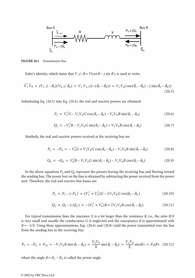
Euler’s identity, which states that V ∠−δ = V(cos δ − j sin δ ), is used to write:
(20.5)
Substituting Eq. (20.5) into Eq. (20.4), the real and reactive powers are obtained:
(20.6)
(20.7)
Similarly, the real and reactive powers received at the receiving bus are
(20.8)
(20.9)
In the above equations PR and QR represent the powers leaving the receiving bus and flowing towardthe sending bus. The power lost on the line is obtained by subtracting the power received from the powersent. Therefore, the real and reactive line losses are
(20.10)
(20.11)
For typical transmission lines the reactance X is a lot larger than the resistance R, i.e., the ratio R/Xis very small and usually the conductance G is neglected and the susceptance B is approximated withB = −1/X. Using these approximations, Eqs. (20.6) and (20.8) yield the power transmitted over the linefrom the sending bus to the receiving bus:
(20.12)
where the angle δ = δ S − δ R is called the power angle.
FIGURE 20.1 Transmission line.
V S∗
V R VS dS–∠( ) VR dR∠( ) V S V R dS dR–( )–( )∠ V SVR dS dR–( )cos j dS dR–( )sin–( )= = =
PS VS2G VSVRG dS dR–( )cos– VSVRB dS dR–( )sin–=
QS V– S2B VSVRG dS dR–( )sin– VSVRB dS dR–( )cos+=
P0 P– R VR2G– VSVRG dS dR–( )cos VSVRB dS dR–( )sin–+= =
Q0 Q– R VR2B VSVRG dS dR–( )sin VSVRB dS dR–( )cos––= =
PL PS PR–( )– VS2 VR
2+( )G 2VSVRG dS dR–( )cos–= =
QL QS QR–( )– – VS2 VR
2+( )B 2VSVRB dS dR–( )cos+= =
PS PR– PSR VSVRB dS dR–( )sin–VSVR
X------------ dS dR–( )sin
VSVR
X------------ d( )sin P0 d( )= = = = = =
© 2002 by CRC Press LLC
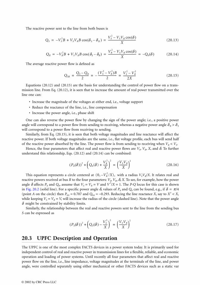
The reactive power sent to the line from both buses is
(20.13)
(20.14)
The average reactive power flow is defined as
(20.15)
Equations (20.12) and (20.15) are the basis for understanding the control of power flow on a trans-mission line. From Eq. (20.12), it is seen that to increase the amount of real power transmitted over theline one can:
• Increase the magnitude of the voltages at either end, i.e., voltage support
• Reduce the reactance of the line, i.e., line compensation
• Increase the power angle, i.e., phase shift
One can also reverse the power flow by changing the sign of the power angle; i.e., a positive powerangle will correspond to a power flow from sending to receiving, whereas a negative power angle δ R > δ S
will correspond to a power flow from receiving to sending.Similarly, from Eq. (20.15), it is seen that both voltage magnitudes and line reactance will affect the
reactive power. If both voltage magnitudes are the same, i.e., flat voltage profile, each bus will send halfof the reactive power absorbed by the line. The power flow is from sending to receiving when VR < VS.
Hence, the four parameters that affect real and reactive power flows are VS, VR, X, and δ. To furtherunderstand this relationship, Eqs. (20.12) and (20.14) can be combined:
(20.16)
This equation represents a circle centered at with a radius VSVR/X. It relates real andreactive powers received at bus R to the four parameters: VS, VR, δ, X. To see, for example, how the powerangle δ affects P0 and Q0, assume that VS = VR = V and V
2/X = 1. The P-Q locus for this case is shown
in Fig. 20.2 (solid line). For a specific power angle δ, values of P0 and Q0 can be found, e.g., if δ = π/4(point A on the circle) then P0A = 0.707 and Q0A = −0.293. Reducing the line reactance X, say to X ′ < X,while keeping VS = VR = V, will increase the radius of the circle (dashed line). Note that the power angleδ might be constrained by stability limits.
Similarly, the relationship between the real and reactive powers sent to the line from the sending busS can be expressed as
(20.17)
20.3 UPFC Description and Operation
The UPFC is one of the most complex FACTS devices in a power system today. It is primarily used forindependent control of real and reactive power in transmission lines for a flexible, reliable, and economicoperation and loading of power systems. Until recently all four parameters that affect real and reactivepower flow on the line, i.e., line impedance, voltage magnitudes at the terminals of the line, and powerangle, were controlled separately using either mechanical or other FACTS devices such as a static var
QS V– S2B VSVRB d S d R–( )cos+
VS2 VSVR d( )cos–
X------------------------------------------= =
QR VR2– B VSVRB dS dR–( )cos+
VR2 VSVR d( )cos–
X------------------------------------------ Q0 d( )–= = =
QSR
QS QR–2
-------------------VS
2 VR2–( )B
2----------------------------–
VS2 VR
2–2X
-------------------= = =
P0 d( )( )2 Q0(d )VR
2
X-------+
2
+VSVR
X------------
2
=
(0, VR2 /X)– ,
PS d( )( )2 QS d( )VS
2
X-------–
2
+VSVR
X------------
2
=
© 2002 by CRC Press LLC
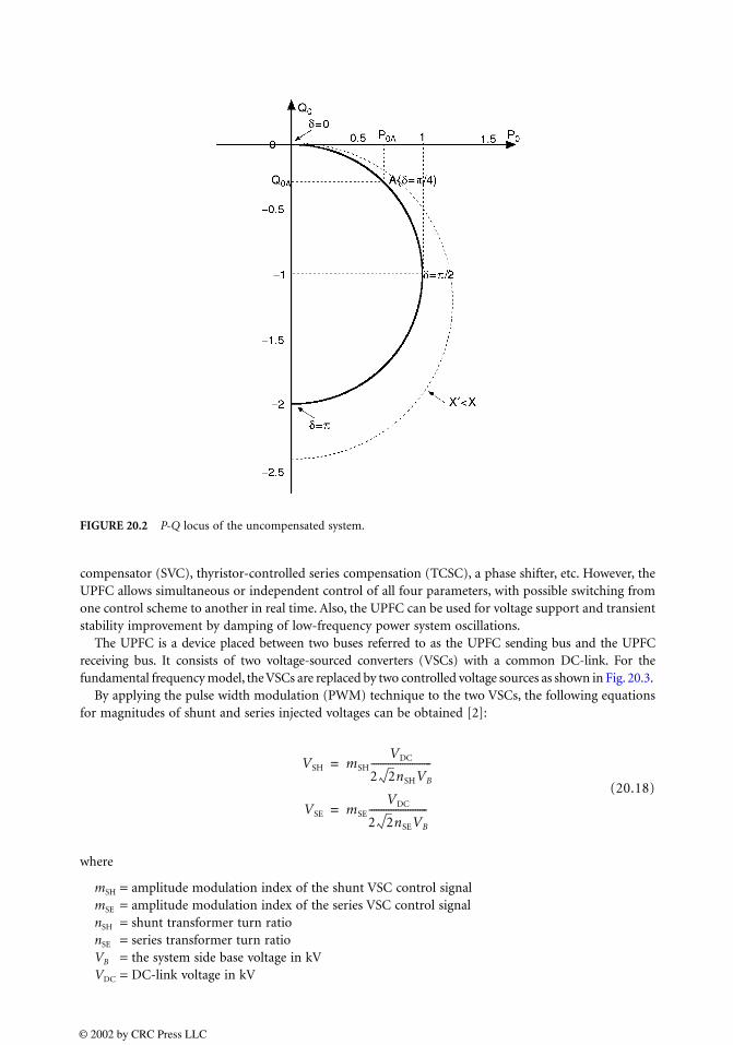
compensator (SVC), thyristor-controlled series compensation (TCSC), a phase shifter, etc. However, theUPFC allows simultaneous or independent control of all four parameters, with possible switching fromone control scheme to another in real time. Also, the UPFC can be used for voltage support and transientstability improvement by damping of low-frequency power system oscillations.
The UPFC is a device placed between two buses referred to as the UPFC sending bus and the UPFCreceiving bus. It consists of two voltage-sourced converters (VSCs) with a common DC-link. For thefundamental frequency model, the VSCs are replaced by two controlled voltage sources as shown in Fig. 20.3.
By applying the pulse width modulation (PWM) technique to the two VSCs, the following equationsfor magnitudes of shunt and series injected voltages can be obtained [2]:
(20.18)
where
mSH = amplitude modulation index of the shunt VSC control signalmSE = amplitude modulation index of the series VSC control signalnSH = shunt transformer turn rationSE = series transformer turn ratioVB = the system side base voltage in kVVDC = DC-link voltage in kV
FIGURE 20.2 P-Q locus of the uncompensated system.
VSH mSH
VDC
2 2nSHVB
-------------------------=
VSE mSE
VDC
2 2nSEVB
------------------------=
© 2002 by CRC Press LLC
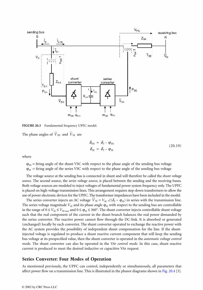
The phase angles of and are
(20.19)
where
ϕSH = firing angle of the shunt VSC with respect to the phase angle of the sending bus voltageϕSE = firing angle of the series VSC with respect to the phase angle of the sending bus voltage
The voltage source at the sending bus is connected in shunt and will therefore be called the shunt voltagesource. The second source, the series voltage source, is placed between the sending and the receiving buses.Both voltage sources are modeled to inject voltages of fundamental power system frequency only. The UPFCis placed on high-voltage transmission lines. This arrangement requires step-down transformers to allow theuse of power electronic devices for the UPFC. The transformer impedances have been included in the model.
The series converter injects an AC voltage = VSE ∠(δS − ϕSE) in series with the transmission line.The series voltage magnitude VSE and its phase angle ϕSE with respect to the sending bus are controllablein the range of 0 ≤ VSE ≤ VSE max and 0 ≤ ϕSE ≤ 360°. The shunt converter injects controllable shunt voltagesuch that the real component of the current in the shunt branch balances the real power demanded bythe series converter. The reactive power cannot flow through the DC-link. It is absorbed or generated(exchanged) locally by each converter. The shunt converter operated to exchange the reactive power withthe AC system provides the possibility of independent shunt compensation for the line. If the shunt-injected voltage is regulated to produce a shunt reactive current component that will keep the sendingbus voltage at its prespecified value, then the shunt converter is operated in the automatic voltage controlmode. The shunt converter can also be operated in the VAr control mode. In this case, shunt reactivecurrent is produced to meet the desired inductive or capacitive VAr request.
Series Converter: Four Modes of Operation
As mentioned previously, the UPFC can control, independently or simultaneously, all parameters thataffect power flow on a transmission line. This is illustrated in the phasor diagrams shown in Fig. 20.4 [3].
FIGURE 20.3 Fundamental frequency UPFC model.
V SH V SE
dSH dS jSH–=dSE dS jSE–=
V SE
© 2002 by CRC Press LLC
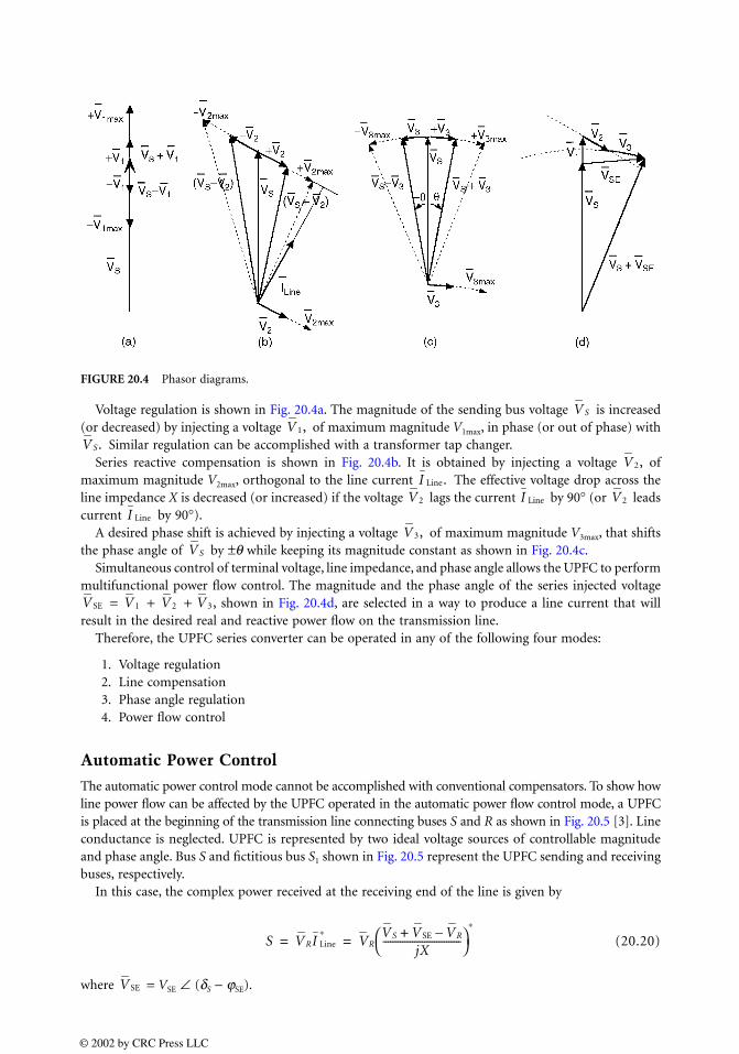
Voltage regulation is shown in Fig. 20.4a. The magnitude of the sending bus voltage is increased(or decreased) by injecting a voltage of maximum magnitude V1max, in phase (or out of phase) with
Similar regulation can be accomplished with a transformer tap changer.Series reactive compensation is shown in Fig. 20.4b. It is obtained by injecting a voltage of
maximum magnitude V2max, orthogonal to the line current The effective voltage drop across theline impedance X is decreased (or increased) if the voltage lags the current by 90° (or leadscurrent by 90°).
A desired phase shift is achieved by injecting a voltage of maximum magnitude V3max, that shiftsthe phase angle of by ±θ while keeping its magnitude constant as shown in Fig. 20.4c.
Simultaneous control of terminal voltage, line impedance, and phase angle allows the UPFC to performmultifunctional power flow control. The magnitude and the phase angle of the series injected voltage
= + + shown in Fig. 20.4d, are selected in a way to produce a line current that willresult in the desired real and reactive power flow on the transmission line.
Therefore, the UPFC series converter can be operated in any of the following four modes:
1. Voltage regulation2. Line compensation3. Phase angle regulation4. Power flow control
Automatic Power Control
The automatic power control mode cannot be accomplished with conventional compensators. To show howline power flow can be affected by the UPFC operated in the automatic power flow control mode, a UPFCis placed at the beginning of the transmission line connecting buses S and R as shown in Fig. 20.5 [3]. Lineconductance is neglected. UPFC is represented by two ideal voltage sources of controllable magnitudeand phase angle. Bus S and fictitious bus S1 shown in Fig. 20.5 represent the UPFC sending and receivingbuses, respectively.
In this case, the complex power received at the receiving end of the line is given by
(20.20)
where = VSE ∠ (δS − ϕSE).
FIGURE 20.4 Phasor diagrams.
V S
V 1,V S.
V 2,I Line.
V 2 I Line V 2
I Line
V 3,V S
V SE V 1 V 2 V 3,
S VRI Line∗
VRVS VSE VR–+
jX--------------------------------
∗
= =
V SE
© 2002 by CRC Press LLC
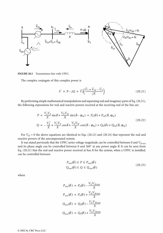
The complex conjugate of this complex power is
(20.21)
By performing simple mathematical manipulations and separating real and imaginary parts of Eq. (20.21),the following expressions for real and reactive powers received at the receiving end of the line are
(20.22)
For VSE = 0 the above equations are identical to Eqs. (20.12) and (20.14) that represent the real andreactive powers of the uncompensated system.
It was stated previously that the UPFC series voltage magnitude can be controlled between 0 and VSE max
and its phase angle can be controlled between 0 and 360° at any power angle δ. It can be seen fromEq. (20.21) that the real and reactive power received at bus R for the system, when a UPFC is installed,can be controlled between
(20.23)
where
FIGURE 20.5 Transmission line with UPFC.
S∗ P jQ– VR∗ VS VSE VR–+
jX--------------------------------
= =
PVSVR
X------------ dsin
VRVSE
X-------------- d jSE–( )sin+ P0 d( ) PSE d, jSE( )+= =
QVR
2
X-------–
VSVR
X------------ dcos
VRVSE
X-------------- d jSE–( )cos+ Q0 d( ) QSE d, jSE( )+=+=
Pmin d( ) P Pmax d( )≤ ≤Qmin d( ) Q Qmax d( )≤ ≤
Pmin d( ) P0 d( )VRVSEmax
X---------------------–=
Pmax d( ) P0 d( )VRVSEmax
X---------------------+=
Qmin d( ) Q0 d( )VRVSEmax
X---------------------–=
Qmax d( ) Q0 d( )VRVSEmax
X---------------------+=
© 2002 by CRC Press LLC
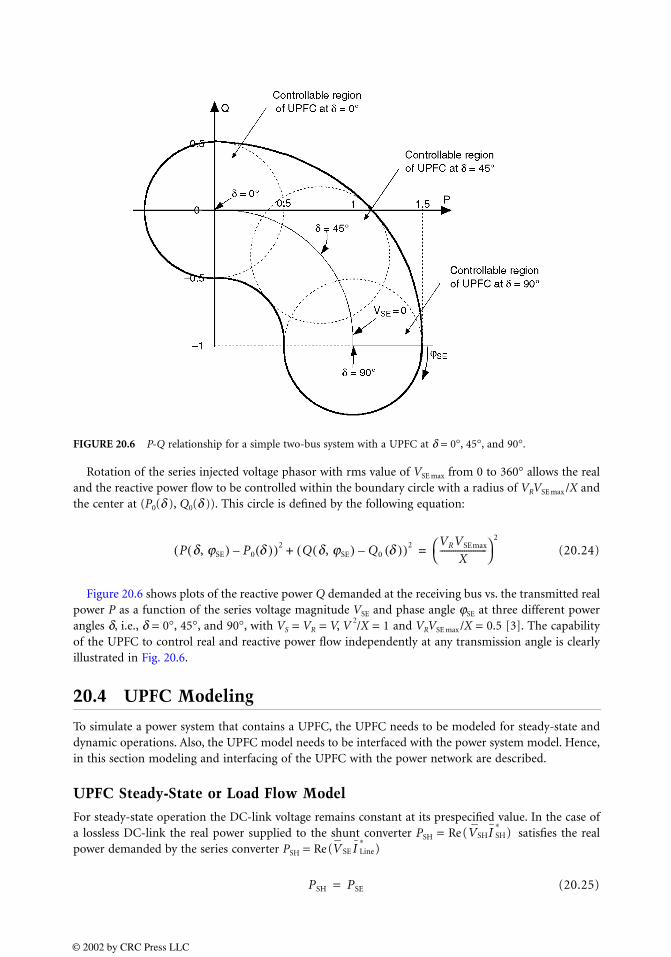
Rotation of the series injected voltage phasor with rms value of VSE max from 0 to 360° allows the realand the reactive power flow to be controlled within the boundary circle with a radius of VRVSE max /X andthe center at (P0(δ ), Q0(δ )). This circle is defined by the following equation:
(20.24)
Figure 20.6 shows plots of the reactive power Q demanded at the receiving bus vs. the transmitted realpower P as a function of the series voltage magnitude VSE and phase angle ϕSE at three different powerangles δ, i.e., δ = 0°, 45°, and 90°, with VS = VR = V, V
2/X = 1 and VRVSE max/X = 0.5 [3]. The capability
of the UPFC to control real and reactive power flow independently at any transmission angle is clearlyillustrated in Fig. 20.6.
20.4 UPFC Modeling
To simulate a power system that contains a UPFC, the UPFC needs to be modeled for steady-state anddynamic operations. Also, the UPFC model needs to be interfaced with the power system model. Hence,in this section modeling and interfacing of the UPFC with the power network are described.
UPFC Steady-State or Load Flow Model
For steady-state operation the DC-link voltage remains constant at its prespecified value. In the case ofa lossless DC-link the real power supplied to the shunt converter PSH = Re satisfies the realpower demanded by the series converter PSH = Re
(20.25)
FIGURE 20.6 P-Q relationship for a simple two-bus system with a UPFC at δ = 0°, 45°, and 90°.
P d, jSE( ) P0 d( )–( )2 Q d, jSE( ) Q0 d( )–( )2+VRVSEmax
X---------------------
2
=
(VSHI SH∗
)(V SE I Line
∗)
PSH PSE=
© 2002 by CRC Press LLC
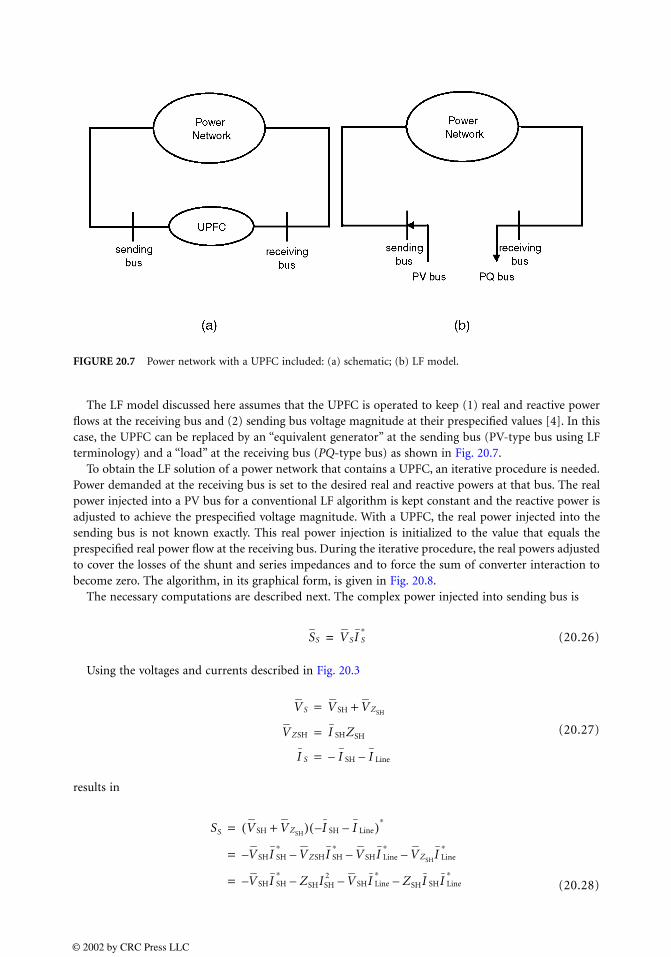
The LF model discussed here assumes that the UPFC is operated to keep (1) real and reactive powerflows at the receiving bus and (2) sending bus voltage magnitude at their prespecified values [4]. In thiscase, the UPFC can be replaced by an “equivalent generator” at the sending bus (PV-type bus using LFterminology) and a “load” at the receiving bus (PQ-type bus) as shown in Fig. 20.7.
To obtain the LF solution of a power network that contains a UPFC, an iterative procedure is needed.Power demanded at the receiving bus is set to the desired real and reactive powers at that bus. The realpower injected into a PV bus for a conventional LF algorithm is kept constant and the reactive power isadjusted to achieve the prespecified voltage magnitude. With a UPFC, the real power injected into thesending bus is not known exactly. This real power injection is initialized to the value that equals theprespecified real power flow at the receiving bus. During the iterative procedure, the real powers adjustedto cover the losses of the shunt and series impedances and to force the sum of converter interaction tobecome zero. The algorithm, in its graphical form, is given in Fig. 20.8.
The necessary computations are described next. The complex power injected into sending bus is
(20.26)
Using the voltages and currents described in Fig. 20.3
(20.27)
results in
(20.28)
FIGURE 20.7 Power network with a UPFC included: (a) schematic; (b) LF model.
SS V SI S∗
=
V S V SH V ZSH+=
V ZSH I SHZSH=
I S I SH– I Line–=
SS V SH V ZSH+( ) I SH I Line––( )∗=
V SH– I SH∗
V ZSHI SH∗
– V SHI Line∗
– V ZSHI Line
∗–=
V– SHI SH∗
ZSHISH2– V SHI Line
∗– ZSHI SHI Line
∗–=
© 2002 by CRC Press LLC
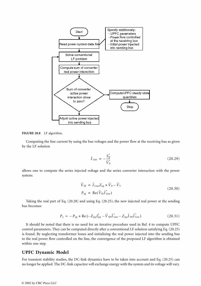
Computing the line current by using the bus voltages and the power flow at the receiving bus as givenby the LF solution
(20.29)
allows one to compute the series injected voltage and the series converter interaction with the powersystem:
(20.30)
Taking the real part of Eq. (20.28) and using Eq. (20.25), the new injected real power at the sendingbus becomes
(20.31)
It should be noted that there is no need for an iterative procedure used in Ref. 4 to compute UPFCcontrol parameters. They can be computed directly after a conventional LF solution satisfying Eq. (20.25)is found. By neglecting transformer losses and initializing the real power injected into the sending busto the real power flow controlled on the line, the convergence of the proposed LF algorithm is obtainedwithin one step.
UPFC Dynamic Model
For transient stability studies, the DC-link dynamics have to be taken into account and Eq. (20.25) canno longer be applied. The DC-link capacitor will exchange energy with the system and its voltage will vary.
FIGURE 20.8 LF algorithm.
I LineSR
∗
V R∗------–=
V SE I LineZSE V R V S–+=
PSE Re VSEI Line∗( )=
PS PSE– Re ZSHISH2– V SHI Line
∗ZSHI SHI Line
∗––( )+=
© 2002 by CRC Press LLC
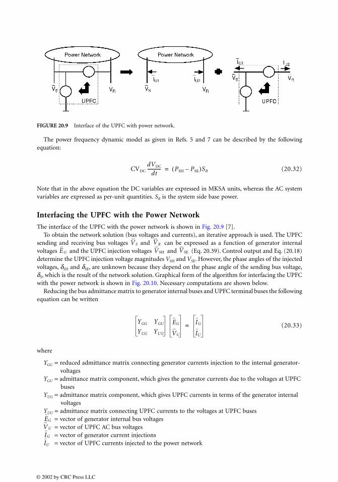
The power frequency dynamic model as given in Refs. 5 and 7 can be described by the followingequation:
(20.32)
Note that in the above equation the DC variables are expressed in MKSA units, whereas the AC systemvariables are expressed as per-unit quantities. SB is the system side base power.
Interfacing the UPFC with the Power Network
The interface of the UPFC with the power network is shown in Fig. 20.9 [7].To obtain the network solution (bus voltages and currents), an iterative approach is used. The UPFC
sending and receiving bus voltages and can be expressed as a function of generator internalvoltages and the UPFC injection voltages and (Eq. 20.39). Control output and Eq. (20.18)determine the UPFC injection voltage magnitudes VSH and VSE. However, the phase angles of the injectedvoltages, δSH and δSE, are unknown because they depend on the phase angle of the sending bus voltage,δS, which is the result of the network solution. Graphical form of the algorithm for interfacing the UPFCwith the power network is shown in Fig. 20.10. Necessary computations are shown below.
Reducing the bus admittance matrix to generator internal buses and UPFC terminal buses the followingequation can be written
(20.33)
where
YGG = reduced admittance matrix connecting generator currents injection to the internal generator-voltages
YGU = admittance matrix component, which gives the generator currents due to the voltages at UPFC buses
YUG = admittance matrix component, which gives UPFC currents in terms of the generator internal voltages
YUU = admittance matrix connecting UPFC currents to the voltages at UPFC buses = vector of generator internal bus voltages = vector of UPFC AC bus voltages = vector of generator current injections
= vector of UPFC currents injected to the power network
FIGURE 20.9 Interface of the UPFC with power network.
CVDC
dVDC
dt------------ PSH PSE–( )SB=
V S V R
E G V SH V SE
YGG YGU
YUG YUU
EG
VU
IG
IU
=
EG
V U
IG
IU
© 2002 by CRC Press LLC
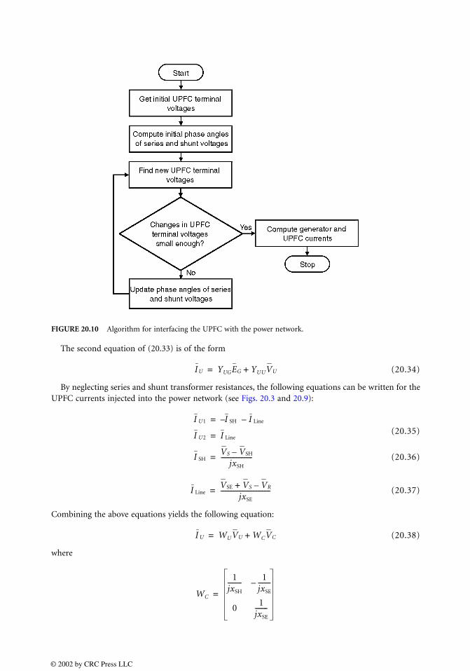
The second equation of (20.33) is of the form
(20.34)
By neglecting series and shunt transformer resistances, the following equations can be written for theUPFC currents injected into the power network (see Figs. 20.3 and 20.9):
(20.35)
(20.36)
(20.37)
Combining the above equations yields the following equation:
(20.38)
where
FIGURE 20.10 Algorithm for interfacing the UPFC with the power network.
I U YUGEG YUUVU+=
I U1 I SH– I Line–=
I U2 I Line=
I SHVS VSH–
jxSH
--------------------=
I LineVSE VS VR–+
jxSE
--------------------------------=
I U WUVU WCVC+=
WC
1jxSH
--------- 1jxSE
--------–
01
jxSE
--------
=
© 2002 by CRC Press LLC

By equating (20.34) with (20.38), the following equation for computation of UPFC terminal voltagescan be written:
(20.39)
20.5 Control Design
To operate the UPFC in the automatic control mode discussed in the previous section, and also to use theUPFC to enhance power system stability and dampen low-frequency oscillations, two control designs needto be performed. A primary control design, referred to as the UPFC basic control design, involves simulta-neous regulation of (1) real and reactive power flows on the transmission line, (2) sending bus voltagemagnitude, and (3) DC voltage magnitude. A secondary control design, referred to as the dampingcontroller design, is a supplementary control loop that is designed to improve transient stability of theentire electric power system. The two control designs are described in this section.
UPFC Basic Control Design
The UPFC basic control design consists of four separate control loops grouped into a series control scheme,whose objective is to maintain both real and reactive power flows on the transmission lines close to someprespecified values, and a shunt control scheme, whose objective is to control the sending bus voltagemagnitude as well as the DC voltage magnitude.
Series Control Scheme
This scheme has two control loops, one for the tracking of the real power flow at the receiving bus ofthe line, and the second performing the same task for the reactive power flow. Specifically, the objectiveis to track these real and reactive power flows following step changes and to eliminate steady-state trackingerrors. This is obtained by the appropriate selection of the voltage drop between the sending and thereceiving buses, which is denoted This voltage can be decomposed into the following two quantities,which affect the tracked powers, namely:
1. VP = voltage component orthogonal to the sending bus voltage (it affects primarily the real powerflow on the transmission line)
2. VQ = component in phase with the sending bus voltage (it affects mainly the reactive power flowon the transmission line)
These quantities are in phasor diagram in Fig. 20.11.
WU
1jxSE
--------– 1jxSH
---------–1
jxSE
--------
1jxSE
-------- 1jxSE
--------–
=
I UI U1
I U2
=
VUVS
VR
=
VCVSH
VSE
=
VU WU YUU–( ) 1– YUGEG WU YUU–( ) 1– WCVC– LGEG LCVC+= =
VPQ.
© 2002 by CRC Press LLC
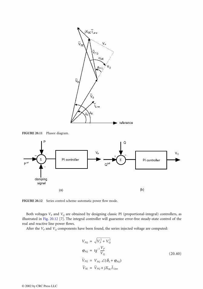
Both voltages VP and VQ are obtained by designing classic PI (proportional-integral) controllers, asillustrated in Fig. 20.12 [7]. The integral controller will guarantee error-free steady-state control of thereal and reactive line power flows.
After the VP and VQ components have been found, the series injected voltage are computed:
(20.40)
FIGURE 20.11 Phasor diagram.
FIGURE 20.12 Series control scheme–automatic power flow mode.
VPQ VP2 VQ
2+=
jPQ tg 1– VP
VQ
------=
VPQ VPQ dS jPQ+( )∠=
VSE VPQ jXSE I Line+=
© 2002 by CRC Press LLC
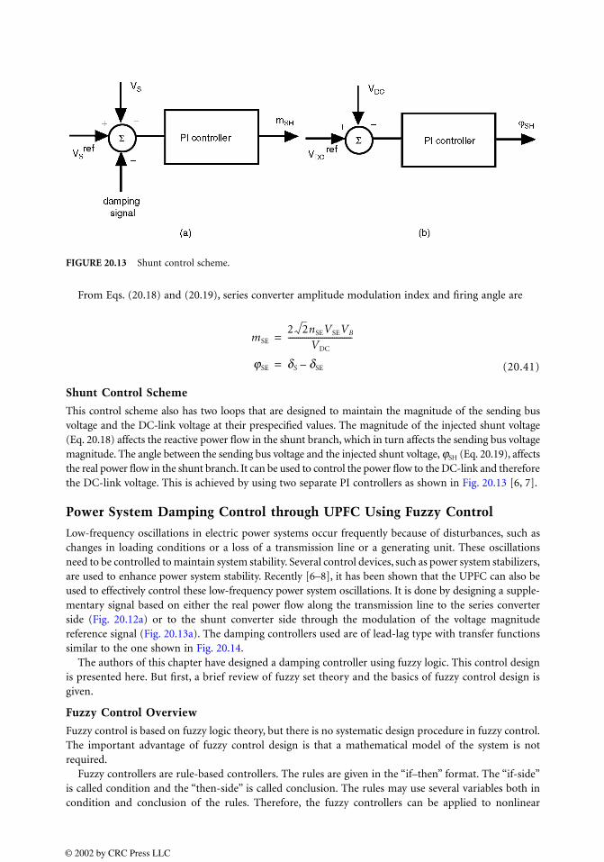
From Eqs. (20.18) and (20.19), series converter amplitude modulation index and firing angle are
(20.41)
Shunt Control Scheme
This control scheme also has two loops that are designed to maintain the magnitude of the sending busvoltage and the DC-link voltage at their prespecified values. The magnitude of the injected shunt voltage(Eq. 20.18) affects the reactive power flow in the shunt branch, which in turn affects the sending bus voltagemagnitude. The angle between the sending bus voltage and the injected shunt voltage, ϕSH (Eq. 20.19), affectsthe real power flow in the shunt branch. It can be used to control the power flow to the DC-link and thereforethe DC-link voltage. This is achieved by using two separate PI controllers as shown in Fig. 20.13 [6, 7].
Power System Damping Control through UPFC Using Fuzzy Control
Low-frequency oscillations in electric power systems occur frequently because of disturbances, such aschanges in loading conditions or a loss of a transmission line or a generating unit. These oscillationsneed to be controlled to maintain system stability. Several control devices, such as power system stabilizers,are used to enhance power system stability. Recently [6–8], it has been shown that the UPFC can also beused to effectively control these low-frequency power system oscillations. It is done by designing a supple-mentary signal based on either the real power flow along the transmission line to the series converterside (Fig. 20.12a) or to the shunt converter side through the modulation of the voltage magnitudereference signal (Fig. 20.13a). The damping controllers used are of lead-lag type with transfer functionssimilar to the one shown in Fig. 20.14.
The authors of this chapter have designed a damping controller using fuzzy logic. This control designis presented here. But first, a brief review of fuzzy set theory and the basics of fuzzy control design isgiven.
Fuzzy Control Overview
Fuzzy control is based on fuzzy logic theory, but there is no systematic design procedure in fuzzy control.The important advantage of fuzzy control design is that a mathematical model of the system is notrequired.
Fuzzy controllers are rule-based controllers. The rules are given in the “if–then” format. The “if-side”is called condition and the “then-side” is called conclusion. The rules may use several variables both incondition and conclusion of the rules. Therefore, the fuzzy controllers can be applied to nonlinear
FIGURE 20.13 Shunt control scheme.
mSE
2 2nSEVSEVB
VDC
--------------------------------=
jSE dS dSE–=
© 2002 by CRC Press LLC

multiinput–multioutput (MIMO) systems such as power systems. The control rules can be found basedon:
• Expert experience and control engineering knowledge of the system
• Learning (e.g., neural networks)
Fuzzy logic has its own terminology, which is reviewed below [10].
Fuzzy set: Let X be a collection of objects, then a fuzzy set A in X is defined as
(20.42)
µA(x) is called the membership function of x in A. It usually takes values in the interval [0, 1]. Thenumerical interval X relevant for the description of a fuzzy variable is called Universe of Discourse.
Operations on fuzzy sets: Let A and B be two fuzzy sets with membership functions µA(x) and µB(x).The AND operator or intersection of two fuzzy sets A and B is a fuzzy set C whose membershipfunction µC(x) is defined as
(20.43)
The OR operator or union of two fuzzy sets A and B is a fuzzy set C whose membership function µC(x)is defined as
(20.44)
Next, the structure of a fuzzy controller is presented. A fuzzy controller structure is shown in Fig. 20.15 [9].The controller is placed between preprocessing and post-processing blocks.
The preprocessing block conditions the inputs, crisp measurements, before they enter the controller.First step in fuzzy controller design is to choose appropriate input and output signals of the controller. Second step is to choose linguistic variables that will describe all input and output variables. Third step is to define membership functions for fuzzy sets. Membership functions can be of different
shape, i.e., triangular, trapezoidal, Gaussian functions, etc.
FIGURE 20.14 Lead–lag controller structure.
FIGURE 20.15 Fuzzy controller structure.
A x, mA x( )( ) x X∈ =
mC x( ) min mA x( ), mB x( ) , x X∈=
mC x( ) max mA x( ), mB x( ) , x X∈=
© 2002 by CRC Press LLC
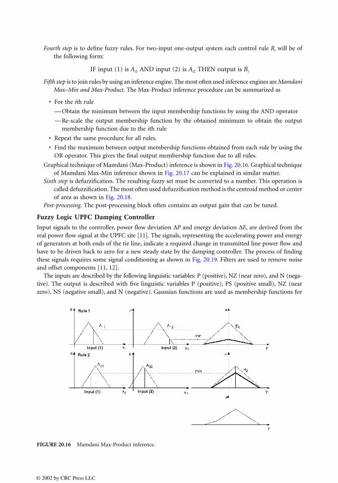
Fourth step is to define fuzzy rules. For two-input one-output system each control rule Ri will be ofthe following form:
IF input (1) is Ai1 AND input (2) is Ai2 THEN output is Bi
Fifth step is to join rules by using an inference engine. The most often used inference engines are MamdaniMax–Min and Max-Product. The Max-Product inference procedure can be summarized as
• For the ith rule
— Obtain the minimum between the input membership functions by using the AND operator
— Re-scale the output membership function by the obtained minimum to obtain the outputmembership function due to the ith rule
• Repeat the same procedure for all rules.
• Find the maximum between output membership functions obtained from each rule by using theOR operator. This gives the final output membership function due to all rules.
Graphical technique of Mamdani (Max-Product) inference is shown in Fig. 20.16. Graphical techniqueof Mamdani Max-Min inference shown in Fig. 20.17 can be explained in similar matter.
Sixth step is defuzzification. The resulting fuzzy set must be converted to a number. This operation iscalled defuzzification. The most often used defuzzification method is the centroid method or centerof area as shown in Fig. 20.18.
Post-processing. The post-processing block often contains an output gain that can be tuned.
Fuzzy Logic UPFC Damping Controller
Input signals to the controller, power flow deviation ∆P and energy deviation ∆E, are derived from thereal power flow signal at the UPFC site [11]. The signals, representing the accelerating power and energyof generators at both ends of the tie line, indicate a required change in transmitted line power flow andhave to be driven back to zero for a new steady state by the damping controller. The process of findingthese signals requires some signal conditioning as shown in Fig. 20.19. Filters are used to remove noiseand offset components [11, 12].
The inputs are described by the following linguistic variables: P (positive), NZ (near zero), and N (nega-tive). The output is described with five linguistic variables P (positive), PS (positive small), NZ (nearzero), NS (negative small), and N (negative). Gaussian functions are used as membership functions for
FIGURE 20.16 Mamdani Max-Product inference.
© 2002 by CRC Press LLC

TABLE 20.1 Fuzzy Rules
if ∆E is NZ, then damping signal is NZif ∆E is P, then damping signal is Pif ∆E is N, then damping signal is Nif ∆E is NZ, and ∆P is P, then damping signal is NSif ∆E is NZ, and ∆P is N, then damping signal is PS
FIGURE 20.17 Mamdani (Max-Min) inference.
FIGURE 20.18 Centroid method.
FIGURE 20.19 Obtaining the input signals for fuzzy controller.
© 2002 by CRC Press LLC
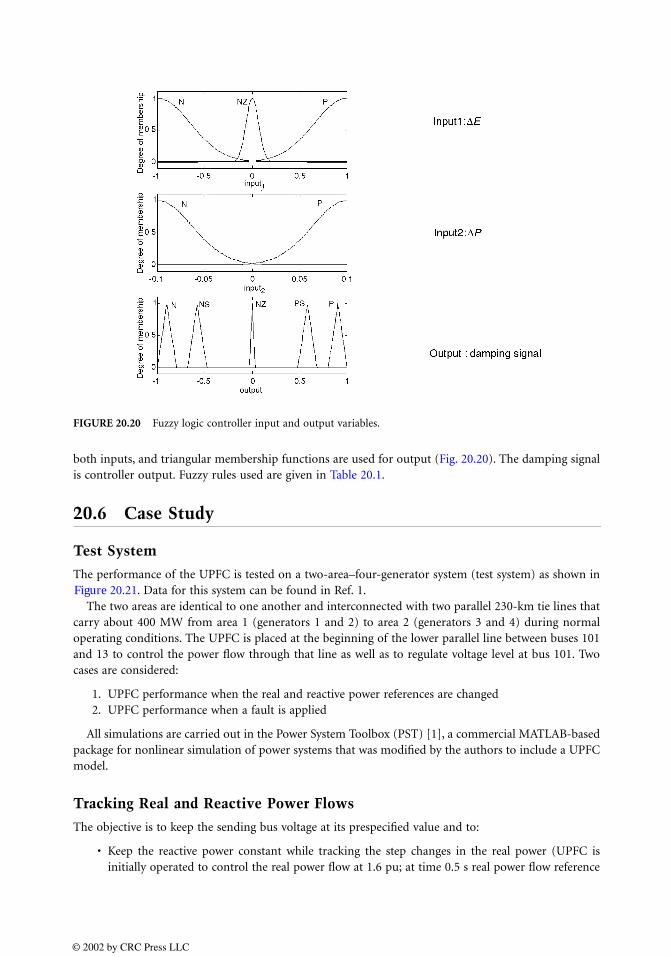
both inputs, and triangular membership functions are used for output (Fig. 20.20). The damping signalis controller output. Fuzzy rules used are given in Table 20.1.
20.6 Case Study
Test System
The performance of the UPFC is tested on a two-area–four-generator system (test system) as shown in Figure 20.21. Data for this system can be found in Ref. 1.
The two areas are identical to one another and interconnected with two parallel 230-km tie lines thatcarry about 400 MW from area 1 (generators 1 and 2) to area 2 (generators 3 and 4) during normaloperating conditions. The UPFC is placed at the beginning of the lower parallel line between buses 101and 13 to control the power flow through that line as well as to regulate voltage level at bus 101. Twocases are considered:
1. UPFC performance when the real and reactive power references are changed2. UPFC performance when a fault is applied
All simulations are carried out in the Power System Toolbox (PST) [1], a commercial MATLAB-basedpackage for nonlinear simulation of power systems that was modified by the authors to include a UPFCmodel.
Tracking Real and Reactive Power Flows
The objective is to keep the sending bus voltage at its prespecified value and to:
• Keep the reactive power constant while tracking the step changes in the real power (UPFC isinitially operated to control the real power flow at 1.6 pu; at time 0.5 s real power flow reference
FIGURE 20.20 Fuzzy logic controller input and output variables.
© 2002 by CRC Press LLC
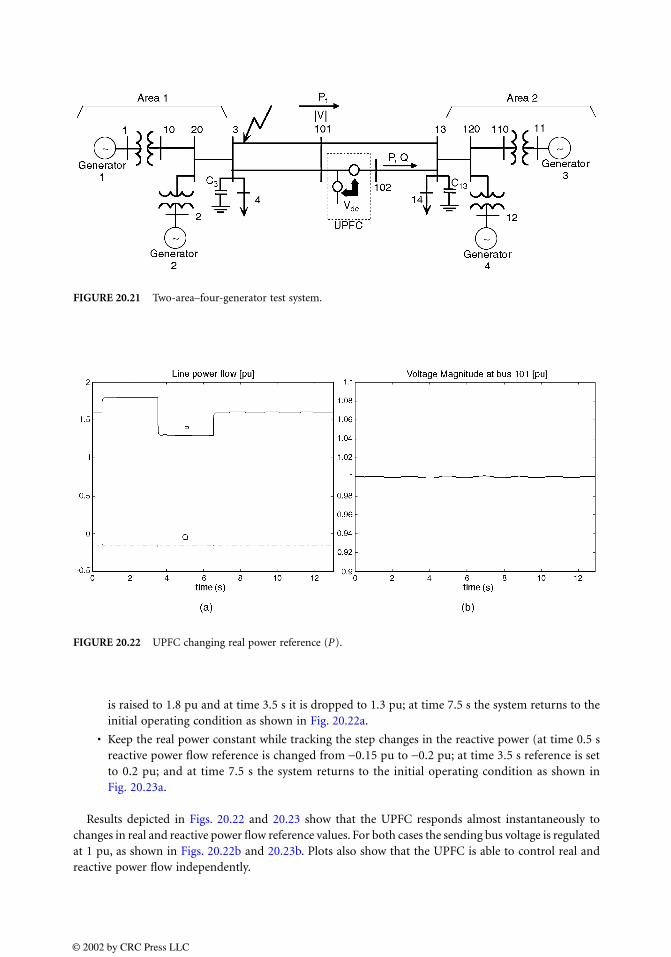
is raised to 1.8 pu and at time 3.5 s it is dropped to 1.3 pu; at time 7.5 s the system returns to theinitial operating condition as shown in Fig. 20.22a.
• Keep the real power constant while tracking the step changes in the reactive power (at time 0.5 sreactive power flow reference is changed from −0.15 pu to −0.2 pu; at time 3.5 s reference is setto 0.2 pu; and at time 7.5 s the system returns to the initial operating condition as shown inFig. 20.23a.
Results depicted in Figs. 20.22 and 20.23 show that the UPFC responds almost instantaneously tochanges in real and reactive power flow reference values. For both cases the sending bus voltage is regulatedat 1 pu, as shown in Figs. 20.22b and 20.23b. Plots also show that the UPFC is able to control real andreactive power flow independently.
FIGURE 20.21 Two-area–four-generator test system.
FIGURE 20.22 UPFC changing real power reference (P).
© 2002 by CRC Press LLC

Operation under Fault Conditions
In this section test system response to a 100-ms three-phase fault applied in area 1, at bus 3, is examined.The fault is cleared by removing one line between the fault bus and bus 101. Two UPFC modes of operationare considered: (1) UPFC operated in the automatic power flow control mode, and (2) UPFC operatedin the power oscillation damping control mode.
UPFC Operated in the Automatic Power Flow Control Mode
For comparison reasons, the test system without the UPFC is simulated first. Simulation results for thetest system with and without UPFC are shown in Fig. 20.24.
During the steady-state operation each interconnecting tie line carries 197 MW (1.97 pu) from area 1to area 2. It can be seen from Fig. 20.24a that the line power flow for the test system without the UPFCoscillates long after the fault is cleared, whereas the desired power flow conditions are reached quicklyafter the fault is cleared for the test system with the UPFC.
For the test system without the UPFC, bus 101 voltage is 0.92 pu, which is below accepted limits.Therefore, the UPFC is operated to keep bus 101 voltage at 1 pu (Fig. 20.24b).
The power angle swings for the test system with UPFC are better damped although it can be seenfrom Fig. 20.24c that constant power flow has negative effect on the system first swing transient, asreported in Ref. 7.
The DC capacitor voltage fluctuation during the transient is less than 1% of its 22-kV rated value(Fig. 20.24d), which is acceptable for this application.
UPFC Operated in the Power Oscillation Damping Control Mode
To improve the power oscillation damping, the UPFC is operated in the automatic power flow mode butwith active damping control. To show the robustness of the proposed control scheme, based on fuzzy logic,discussed earlier, different operating conditions were simulated. The real power that each interconnectingtie-line carries during prefault operating conditions, from area 1 to area 2, is given in Table 20.2.
The fuzzy damping controller is applied to the series converter side. The inputs to the controller arederived from the total real power flow Pt at the UPFC sending bus, as shown in Fig. 20.21. The Max-Product inference engine was used and the centroid defuzzification method was applied. The resultsobtained with the fuzzy controller are compared with those obtained with the lead-lag controller applied
FIGURE 20.23 UPFC changing reactive power reference value (Q).
© 2002 by CRC Press LLC
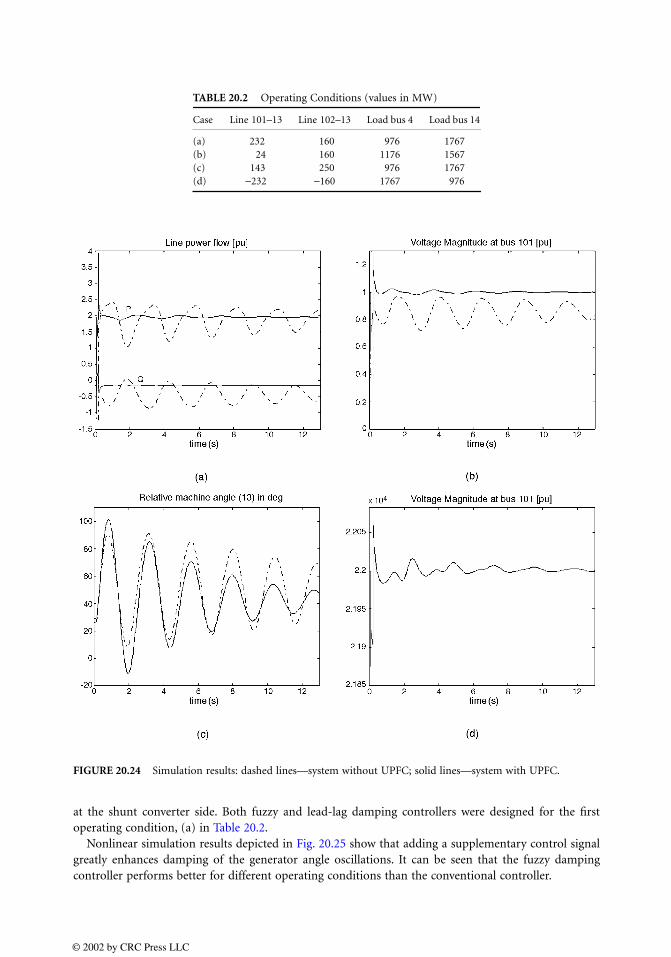
at the shunt converter side. Both fuzzy and lead-lag damping controllers were designed for the firstoperating condition, (a) in Table 20.2.
Nonlinear simulation results depicted in Fig. 20.25 show that adding a supplementary control signalgreatly enhances damping of the generator angle oscillations. It can be seen that the fuzzy dampingcontroller performs better for different operating conditions than the conventional controller.
TABLE 20.2 Operating Conditions (values in MW)
Case Line 101–13 Line 102–13 Load bus 4 Load bus 14
(a) 232 160 976 1767(b) 24 160 1176 1567(c) 143 250 976 1767(d) −232 −160 1767 976
FIGURE 20.24 Simulation results: dashed lines—system without UPFC; solid lines—system with UPFC.
© 2002 by CRC Press LLC
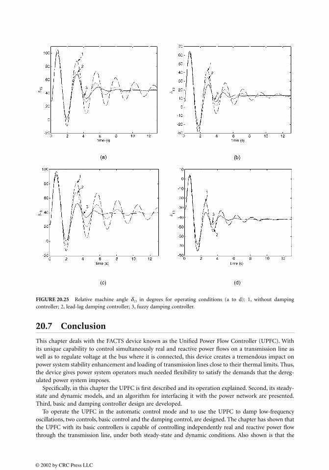
20.7 Conclusion
This chapter deals with the FACTS device known as the Unified Power Flow Controller (UPFC). Withits unique capability to control simultaneously real and reactive power flows on a transmission line aswell as to regulate voltage at the bus where it is connected, this device creates a tremendous impact onpower system stability enhancement and loading of transmission lines close to their thermal limits. Thus,the device gives power system operators much needed flexibility to satisfy the demands that the dereg-ulated power system imposes.
Specifically, in this chapter the UPFC is first described and its operation explained. Second, its steady-state and dynamic models, and an algorithm for interfacing it with the power network are presented.Third, basic and damping controller design are developed.
To operate the UPFC in the automatic control mode and to use the UPFC to damp low-frequencyoscillations, two controls, basic control and the damping control, are designed. The chapter has shown thatthe UPFC with its basic controllers is capable of controlling independently real and reactive power flowthrough the transmission line, under both steady-state and dynamic conditions. Also shown is that the
FIGURE 20.25 Relative machine angle δ13 in degrees for operating conditions (a to d): 1, without dampingcontroller; 2, lead-lag damping controller; 3, fuzzy damping controller.
© 2002 by CRC Press LLC

UPFC can be used for voltage support and for improvement of transient stability of the entire electric powerthrough a supplementary control loop. The proposed supplementary control, based on fuzzy control, iseffective in damping power oscillations. The controller requires only a local measurement—the tie-linepower flow at the UPFC location. Simulation results have shown that controller exhibits good dampingcharacteristics for different operating conditions and performs better than conventional controllers. Theperformance is illustrated with a two-area–four-generator test system. Simulation is performed using theMATLAB-based Power System Toolbox package, which is modified to incorporate the UPFC model.
Acknowledgment
The National Science Foundation under Grant ECS-9870041, and the Department of Energy under aDOE/EPSCoR WV State Implementation Award, sponsored some of the research presented in thischapter.
References
1. Dynamic Tutorial and Functions, Power System Toolbox, Version 2.0, Cherry Tree Scientific Software,Ontario, Canada.
2. Mohan, N., Undeland, T. M., and Robbins, W. P., Power Electronics: Converters, Applications andDesign, 2nd ed., John Wiley & Sons, New York, 1995.
3. Hingorani, N. G. and Gyugyi, L., Understanding FACTS Devices, IEEE Press, New York, 2000.4. Nabavi-Niaki, A. and Iravani, M. R., Steady-state and dynamic models of unified power flow controller
(UPFC) for power system studies, IEEE Trans. Power Syst., 11(4), 1937–1943, 1996.5. Uzunovic, E., Canizares, C. A., and Reeve, J., Fundamental frequency model of unified power flow
controller, in Proceedings of the North American Power Symposium (NAPS), Cleveland, OH, October1998.
6. Uzunovic, E., Canizares, C. A., and Reeve, J., EMTP studies of UPFC power oscillation damping, inProceedings of the North American Power Symposium (NAPS), San Luis Obispo, CA, October 1999,405–410.
7. Huang, Z., Ni, Y., Shen, C. M., Wu, F. F., Chen, S., and Zhang, B., Application of unified power flowcontroller in interconnected power systems—modeling, interface, control strategy and case study,presented at IEEE Power Eng. Society Summer Meeting, 1999.
8. Wang, H. F., Applications of modeling UPFC into multi-machine power systems, IEE Proc. Gener-ation Transmission Distribution, 146(3), 306–312, 1999.
9. Jantzen, J., Design of fuzzy controllers, Technical Report No. 98-E 864 (design), Department ofAutomation, Technical University of Denmark, Lyngby, August 1998.
10. Hsu, Y. Y. and Cheng, C. H, Design of fuzzy power system stabilizers for multimachine power systems,IEE Proc., 137C(3), 233–238, 1990.
11. Hiyama, T., Hubbi, W., and Ortmeyer, T., Fuzzy logic control scheme with variable gain for staticVar compensator to enhance power system stability, IEEE Trans. Power Syst., 14(1), 186–191, 1999.
12. Hiyama, T., Fuzzy logic switching of thyristor controlled braking resistor considering coordinationwith SVC, IEEE Trans. Power Delivery, 10(4), 2020–2026, 1995.
© 2002 by CRC Press LLC
21More-Electric Vehicles
21.1 AircraftConventional Electrical Loads • Power Generation Systems • Aircraft Electrical Distribution Systems • Advanced Electrical Loads • Advanced Electrical Distribution System Architectures • Conclusions
21.2 Terrestrial VehiclesElectrical Power Systems of Conventional Cars • Advanced Electrical Loads • Increasing the System Voltage •Advanced Distribution Systems • Electrical Power Systems of Electric and Hybrid Electric Vehicles • Automotive Electric Motor Drives • Conclusions
21.1 Aircraft
Ali Emadi and Mehrdad Ehsani
Mechanical, electrical, and centralized hydraulic and pneumatic systems are conventional power transfersystems in an aircraft. The More-Electric Aircraft (MEA) concept emphasizes utilizing electrical systemsto replace more aircraft conventional power transfer systems and to facilitate new introduced electricalloads. Improving reliability, maintainability, supportability, survivability, performance, safety, emissions,and operating costs are the main motivations behind the MEA concept.
Conventional Electrical Loads
The power needed for the subsystems in an aircraft is currently derived from mechanical, electrical,hydraulic, and pneumatic sources or a combination of them [1–3]. Generally, hydraulic power transfersystems are used for most of the actuators. On the other hand, pneumatic power transfer systems aremainly employed for air-conditioning, pressurization, and ice protection systems.
Electrical and electronic systems are usually used for avionics and utility functions, such as air datainstruments, communications, landing gear, lighting, navigation, and comfort of the passengers. Otherconventional subsystems that are driven by the electrical sources include energy storage, engine starting,ignition, anti-skid control, and deicing and anti-icing systems [3].
Power Generation Systems
The wound-field synchronous machine has traditionally been used to generate AC electrical power withconstant frequency of 400 Hz. This machine/drive system is known as a constant-speed drive (CSD)system [3–5]. Figure 21.1 shows a typical constant-speed drive system. In Fig. 21.1, synchronous gener-ators supply AC constant-frequency voltage to the AC loads in the aircraft. Then, AC-DC rectifiers areused to convert the AC voltage with fixed frequency at the main AC bus to multilevel DC voltages at the
Ali EmadiIllinois Institute of Technology
Mehrdad EhsaniTexas A&M University
© 2002 by CRC Press LLC
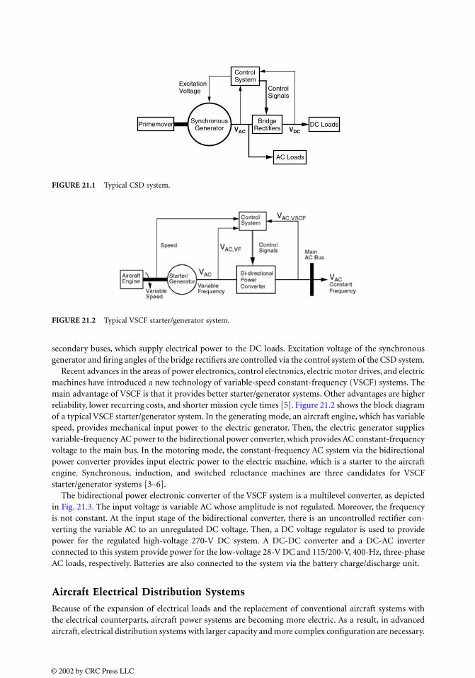
secondary buses, which supply electrical power to the DC loads. Excitation voltage of the synchronousgenerator and firing angles of the bridge rectifiers are controlled via the control system of the CSD system.
Recent advances in the areas of power electronics, control electronics, electric motor drives, and electricmachines have introduced a new technology of variable-speed constant-frequency (VSCF) systems. Themain advantage of VSCF is that it provides better starter/generator systems. Other advantages are higherreliability, lower recurring costs, and shorter mission cycle times [5]. Figure 21.2 shows the block diagramof a typical VSCF starter/generator system. In the generating mode, an aircraft engine, which has variablespeed, provides mechanical input power to the electric generator. Then, the electric generator suppliesvariable-frequency AC power to the bidirectional power converter, which provides AC constant-frequencyvoltage to the main bus. In the motoring mode, the constant-frequency AC system via the bidirectionalpower converter provides input electric power to the electric machine, which is a starter to the aircraftengine. Synchronous, induction, and switched reluctance machines are three candidates for VSCFstarter/generator systems [3–6].
The bidirectional power electronic converter of the VSCF system is a multilevel converter, as depictedin Fig. 21.3. The input voltage is variable AC whose amplitude is not regulated. Moreover, the frequencyis not constant. At the input stage of the bidirectional converter, there is an uncontrolled rectifier con-verting the variable AC to an unregulated DC voltage. Then, a DC voltage regulator is used to providepower for the regulated high-voltage 270-V DC system. A DC-DC converter and a DC-AC inverterconnected to this system provide power for the low-voltage 28-V DC and 115/200-V, 400-Hz, three-phaseAC loads, respectively. Batteries are also connected to the system via the battery charge/discharge unit.
Aircraft Electrical Distribution Systems
Because of the expansion of electrical loads and the replacement of conventional aircraft systems withthe electrical counterparts, aircraft power systems are becoming more electric. As a result, in advancedaircraft, electrical distribution systems with larger capacity and more complex configuration are necessary.
FIGURE 21.1 Typical CSD system.
FIGURE 21.2 Typical VSCF starter/generator system.
Primemover SynchronousGenerator
BridgeRectifiers
DC Loads
ControlSystem
AC Loads
ExcitationVoltage
VAC VDC
ControlSignals
© 2002 by CRC Press LLC
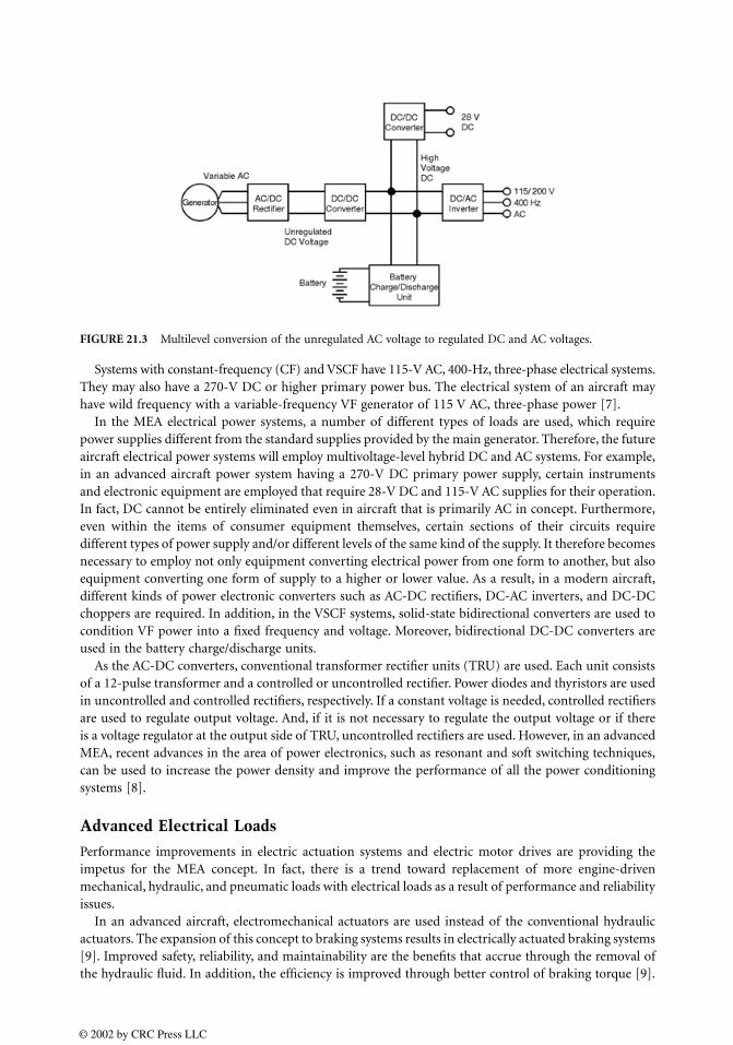
Systems with constant-frequency (CF) and VSCF have 115-V AC, 400-Hz, three-phase electrical systems.They may also have a 270-V DC or higher primary power bus. The electrical system of an aircraft mayhave wild frequency with a variable-frequency VF generator of 115 V AC, three-phase power [7].
In the MEA electrical power systems, a number of different types of loads are used, which requirepower supplies different from the standard supplies provided by the main generator. Therefore, the futureaircraft electrical power systems will employ multivoltage-level hybrid DC and AC systems. For example,in an advanced aircraft power system having a 270-V DC primary power supply, certain instrumentsand electronic equipment are employed that require 28-V DC and 115-V AC supplies for their operation.In fact, DC cannot be entirely eliminated even in aircraft that is primarily AC in concept. Furthermore,even within the items of consumer equipment themselves, certain sections of their circuits requiredifferent types of power supply and/or different levels of the same kind of the supply. It therefore becomesnecessary to employ not only equipment converting electrical power from one form to another, but alsoequipment converting one form of supply to a higher or lower value. As a result, in a modern aircraft,different kinds of power electronic converters such as AC-DC rectifiers, DC-AC inverters, and DC-DCchoppers are required. In addition, in the VSCF systems, solid-state bidirectional converters are used tocondition VF power into a fixed frequency and voltage. Moreover, bidirectional DC-DC converters areused in the battery charge/discharge units.
As the AC-DC converters, conventional transformer rectifier units (TRU) are used. Each unit consistsof a 12-pulse transformer and a controlled or uncontrolled rectifier. Power diodes and thyristors are usedin uncontrolled and controlled rectifiers, respectively. If a constant voltage is needed, controlled rectifiersare used to regulate output voltage. And, if it is not necessary to regulate the output voltage or if thereis a voltage regulator at the output side of TRU, uncontrolled rectifiers are used. However, in an advancedMEA, recent advances in the area of power electronics, such as resonant and soft switching techniques,can be used to increase the power density and improve the performance of all the power conditioningsystems [8].
Advanced Electrical Loads
Performance improvements in electric actuation systems and electric motor drives are providing theimpetus for the MEA concept. In fact, there is a trend toward replacement of more engine-drivenmechanical, hydraulic, and pneumatic loads with electrical loads as a result of performance and reliabilityissues.
In an advanced aircraft, electromechanical actuators are used instead of the conventional hydraulicactuators. The expansion of this concept to braking systems results in electrically actuated braking systems[9]. Improved safety, reliability, and maintainability are the benefits that accrue through the removal ofthe hydraulic fluid. In addition, the efficiency is improved through better control of braking torque [9].
FIGURE 21.3 Multilevel conversion of the unregulated AC voltage to regulated DC and AC voltages.
© 2002 by CRC Press LLC

Furthermore, conventional aeroengine actuators use fluid power in the form of pneumatic, hydraulic,or fueldraulics to provide the motive effort. There is also a trend toward replacing these traditionalhydraulic/pneumatic/fueldraulic engine actuation systems with electromechanical actuators. The mainadvantages are easier interfacing, reduced maintenance costs, lighter systems, and improved reliability.The electric motor type selected is a three-phase brushless DC motor [10].
Some of the other loads considered are electromechanical and electrohydraulic flight control actuators,270-V DC switched reluctance starter/generators, electric anti-icing systems, environmental systems,electromechanical valve controllers, air-conditioning systems, utility actuators, weapon systems, anddifferent electric motor drives for pumps and other applications. In fact, electrical subsystems may requirea lower engine power with higher efficiency. Also, they can be used only when needed. Therefore, MEAcan have better fuel economy and performance. Figure 21.4 shows the main electrical power subsystemsin the MEA power systems.
Advanced Electrical Distribution System Architectures
A conventional distribution network is a point-to-point topology in which all the electrical wires aredistributed from the main bus to different loads through relays and switches. This kind of distributionnetwork leads to expensive, complicated, and heavy wiring circuits. However, in an advanced aircraft,loads are controlled by intelligent remote modules. Therefore, the number and length of wires in theharness are reduced. Furthermore, by interconnection between remote modules via communication/con-trol buses, it is possible to have a power management system (PMS). The primary function of the PMSis time-phasing of the duty cycle of loads to reduce the peak power demand [11]. Other functions of thePMS are battery management and charging strategy in a multiple-battery system, load management,management of the starter/generator system including the regulator, and provision and control of a high-integrity supply system. In addition, power management strategy can help optimize the size of thegenerators and batteries [11].
Figure 21.5 shows an advanced aircraft power system architecture in which there are several powerelectronic converters. The distribution control network of Fig. 21.5 simplifies vehicle physical design andassembly and offers additional benefits from the integration with intelligent power management control.Other advantages of this MEA technology are reduced design complexity, fewer flight test hours, reducedground support equipment, and easier aircraft modification [7].
To power important systems in the case of an emergency, permanent magnet (PM) generators areused to generate 28-V DC voltage. Furthermore, the main distribution system can also be changed fromDC to AC. The main advantage of AC distribution systems is easy conversion to different voltage levelsby transformers. Also, AC machines are easy to use.
FIGURE 21.4 MEA electrical power subsystems.
© 2002 by CRC Press LLC
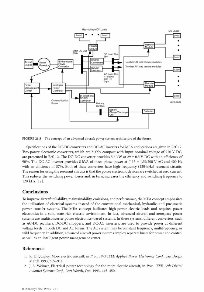
Specifications of the DC-DC converters and DC-AC inverters for MEA applications are given in Ref. 12.Two power electronic converters, which are highly compact with input nominal voltage of 270 V DC,are presented in Ref. 12. The DC-DC converter provides 5.6 kW at 29 ± 0.5 V DC with an efficiency of90%. The DC-AC inverter provides 8 kVA of three-phase power at (115 ± 1.5)/200 V AC and 400 Hzwith an efficiency of 87%. Both of these converters have high-frequency (120-kHz) resonant circuits.The reason for using the resonant circuits is that the power electronic devices are switched at zero current.This reduces the switching power losses and, in turn, increases the efficiency and switching frequency to120 kHz [12].
Conclusions
To improve aircraft reliability, maintainability, emissions, and performance, the MEA concept emphasizesthe utilization of electrical systems instead of the conventional mechanical, hydraulic, and pneumaticpower transfer systems. The MEA concept facilitates high-power electric loads and requires powerelectronics in a solid-state rich electric environment. In fact, advanced aircraft and aerospace powersystems are multiconverter power electronics–based systems. In these systems, different converters, suchas AC-DC rectifiers, DC-DC choppers, and DC-AC inverters, are used to provide power at differentvoltage levels in both DC and AC forms. The AC system may be constant frequency, multifrequency, orwild frequency. In addition, advanced aircraft power systems employ separate buses for power and controlas well as an intelligent power management center.
References
1. R. E. Quigley, More electric aircraft, in Proc. 1993 IEEE Applied Power Electronics Conf., San Diego,March 1993, 609–911.
2. J. A. Weimer, Electrical power technology for the more electric aircraft, in Proc. IEEE 12th DigitalAvionics Systems Conf., Fort Worth, Oct. 1993, 445–450.
FIGURE 21.5 The concept of an advanced aircraft power system architecture of the future.
© 2002 by CRC Press LLC
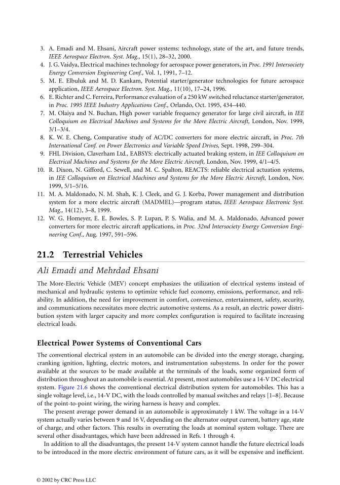
3. A. Emadi and M. Ehsani, Aircraft power systems: technology, state of the art, and future trends,IEEE Aerospace Electron. Syst. Mag., 15(1), 28–32, 2000.
4. J. G. Vaidya, Electrical machines technology for aerospace power generators, in Proc. 1991 IntersocietyEnergy Conversion Engineering Conf., Vol. 1, 1991, 7–12.
5. M. E. Elbuluk and M. D. Kankam, Potential starter/generator technologies for future aerospaceapplication, IEEE Aerospace Electron. Syst. Mag., 11(10), 17–24, 1996.
6. E. Richter and C. Ferreira, Performance evaluation of a 250 kW switched reluctance starter/generator,in Proc. 1995 IEEE Industry Applications Conf., Orlando, Oct. 1995, 434–440.
7. M. Olaiya and N. Buchan, High power variable frequency generator for large civil aircraft, in IEEColloquium on Electrical Machines and Systems for the More Electric Aircraft, London, Nov. 1999,3/1–3/4.
8. K. W. E. Cheng, Comparative study of AC/DC converters for more electric aircraft, in Proc. 7thInternational Conf. on Power Electronics and Variable Speed Drives, Sept. 1998, 299–304.
9. FHL Division, Claverham Ltd., EABSYS: electrically actuated braking system, in IEE Colloquium onElectrical Machines and Systems for the More Electric Aircraft, London, Nov. 1999, 4/1–4/5.
10. R. Dixon, N. Gifford, C. Sewell, and M. C. Spalton, REACTS: reliable electrical actuation systems,in IEE Colloquium on Electrical Machines and Systems for the More Electric Aircraft, London, Nov.1999, 5/1–5/16.
11. M. A. Maldonado, N. M. Shah, K. J. Cleek, and G. J. Korba, Power management and distributionsystem for a more electric aircraft (MADMEL)—program status, IEEE Aerospace Electronic Syst.Mag., 14(12), 3–8, 1999.
12. W. G. Homeyer, E. E. Bowles, S. P. Lupan, P. S. Walia, and M. A. Maldonado, Advanced powerconverters for more electric aircraft applications, in Proc. 32nd Intersociety Energy Conversion Engi-neering Conf., Aug. 1997, 591–596.
21.2 Terrestrial Vehicles
Ali Emadi and Mehrdad Ehsani
The More-Electric Vehicle (MEV) concept emphasizes the utilization of electrical systems instead ofmechanical and hydraulic systems to optimize vehicle fuel economy, emissions, performance, and reli-ability. In addition, the need for improvement in comfort, convenience, entertainment, safety, security,and communications necessitates more electric automotive systems. As a result, an electric power distri-bution system with larger capacity and more complex configuration is required to facilitate increasingelectrical loads.
Electrical Power Systems of Conventional Cars
The conventional electrical system in an automobile can be divided into the energy storage, charging,cranking ignition, lighting, electric motors, and instrumentation subsystems. In order for the poweravailable at the sources to be made available at the terminals of the loads, some organized form ofdistribution throughout an automobile is essential. At present, most automobiles use a 14-V DC electricalsystem. Figure 21.6 shows the conventional electrical distribution system for automobiles. This has asingle voltage level, i.e., 14-V DC, with the loads controlled by manual switches and relays [1–8]. Becauseof the point-to-point wiring, the wiring harness is heavy and complex.
The present average power demand in an automobile is approximately 1 kW. The voltage in a 14-Vsystem actually varies between 9 and 16 V, depending on the alternator output current, battery age, stateof charge, and other factors. This results in overrating the loads at nominal system voltage. There areseveral other disadvantages, which have been addressed in Refs. 1 through 4.
In addition to all the disadvantages, the present 14-V system cannot handle the future electrical loadsto be introduced in the more electric environment of future cars, as it will be expensive and inefficient.
© 2002 by CRC Press LLC

Advanced Electrical Loads
In More-Electric Cars (MEC), there is a trend toward expanding electrical loads and replacement of moreengine-driven mechanical and hydraulic systems with electrical systems. These loads include the well-known lights, pumps, fans, and electric motors for various functions. They will also include some lesswell known loads, such as electrically assisted power steering, electrically driven air-conditioner com-pressor, electromechanical valve control, electrically controlled suspension and vehicle dynamics, andelectrically heated catalytic converter. In fact, electrical subsystems may require a lower engine power withhigher efficiency. Furthermore, they can be used only when needed. Therefore, MEC can have optimumfuel economy and performance. There are also other loads such as antilock braking, throttle actuation,ride-height adjustment, and rear-wheel steering, which will be driven electrically in the future.
Figure 21.7 shows electrical loads in the MEC power systems. As is described in Refs. 5 through 8,most of the future electic loads require power electronic controls. In future automobiles, power electronicswill be used to perform three different tasks. The first task is simple on/off switching of loads, which isperformed by mechanical switches and relays in conventional cars. The second task is the control ofelectric machines. The third task is not only changing the system voltage to a higher or lower level, butalso converting electrical power from one form to another using DC-DC, DC-AC, and AC-DC converters.
Increasing the System Voltage
Because of the increasing electrical loads, automotive systems are becoming more electric. Therefore,MEC will need highly reliable, fault-tolerant, autonomously controlled electrical power systems to deliverhigh-quality power from the sources to the loads. The voltage level and form in which power is distributedare important. A higher voltage such as the proposed 42 V will reduce the weight and volume of thewiring harness, among several other advantages [4, 5]. In fact, increasing the voltage of the system, whichis 14 V in conventional cars, is necessary to cope with the greater loads associated with the more electricenvironments in future cars. The near-future average power demand is anticipated to be 3 kW and higher.
Figure 21.8 shows the concept of a dual-voltage automotive power system architecture of the futureMEC. Indeed, it is a transitional two-voltage system, which can be introduced until all automotivecomponents evolve to 42 V. Finally, the future MEC power system will most likely be a single-voltagebus (42 V DC) with provision for hybrid (DC and AC), multivoltage level distribution, and intelligentenergy and load management.
Advanced Distribution Systems
The conventional automotive electrical power system is a point-to-point topology in which all the electricalwiring is distributed from the main bus to different loads through relays and switches of the dashboardcontrol. As a result, the distribution network has expensive, complicated, and heavy wiring circuits.
FIGURE 21.6 Conventional 14-V DC distribution system architecture.
© 2002 by CRC Press LLC

However, in the advanced automotive electrical systems, multiplexed architectures with separate powerand communication buses are used to improve the system. In a multiplexed network, loads are controlledby intelligent remote modules. Therefore, the number and length of wires in tthe harness are reduced.In addition, these systems have a power management system (PMS). The primary function of the PMS istime-phasing of the duty cycle of loads to reduce the peak power demand. Other functions of the PMSare battery management, load management, and management of the starter/generator system includingthe regulator. Figure 21.9 shows typical inputs and outputs of a power management center.
Figure 21.10 shows advanced multiplexed automotive power system architectures of the future withpower and communication buses. The distribution control network of Fig. 21.10 simplifies vehiclephysical design and assembly and offers additional benefits from the integration with intelligent powermanagement control.
Electrical Power Systems of Electric and Hybrid Electric Vehicles
Because of environmental concerns, there is a significant impetus toward development of new propulsionsystems for future cars in the form of electric and hybrid electric vehicles (EV and HEV). Electric vehiclesare known as zero-emission vehicles. They use batteries as electrical energy storage devices and electricmotors to propel the automobile. On the other hand, hybrid vehicles combine more than one energysource for propulsion. In heat engine/battery hybrid systems, the mechanical power available from the
FIGURE 21.7 Electrical loads in MEC power systems.
FIGURE 21.8 The concept of a dual-voltage automotive power system architecture of the future MEC.
s
© 2002 by CRC Press LLC
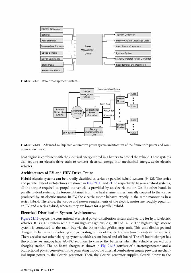
heat engine is combined with the electrical energy stored in a battery to propel the vehicle. These systemsalso require an electric drive train to convert electrical energy into mechanical energy, as do electricvehicles.
Architectures of EV and HEV Drive Trains
Hybrid electric systems can be broadly classified as series or parallel hybrid systems [9–12]. The seriesand parallel hybrid architectures are shown in Figs. 21.11 and 21.12, respectively. In series hybrid systems,all the torque required to propel the vehicle is provided by an electric motor. On the other hand, inparallel hybrid systems, the torque obtained from the heat engine is mechanically coupled to the torqueproduced by an electric motor. In EV, the electric motor behaves exactly in the same manner as in aseries hybrid. Therefore, the torque and power requirements of the electric motor are roughly equal foran EV and a series hybrid, whereas they are lower for a parallel hybrid.
Electrical Distribution System Architectures
Figure 21.13 depicts the conventional electrical power distribution system architecture for hybrid electricvehicles. It is a DC system with a main high-voltage bus, e.g., 300 or 140 V. The high-voltage storagesystem is connected to the main bus via the battery charge/discharge unit. This unit discharges andcharges the batteries in motoring and generating modes of the electric machine operation, respectively.There are also two other charging systems, which are on-board and off-board. The off-board charger hasthree-phase or single-phase AC-DC rectifiers to charge the batteries when the vehicle is parked at acharging station. The on-board charger, as shown in Fig. 21.13 consists of a starter/generator and abidirectional power converter. In the generating mode, the internal combustion engine provides mechan-ical input power to the electric generator. Then, the electric generator supplies electric power to the
FIGURE 21.9 Power management system.
FIGURE 21.10 Advanced multiplexed automotive power system architectures of the future with power and com-munication buses.
Traction Controller
© 2002 by CRC Press LLC
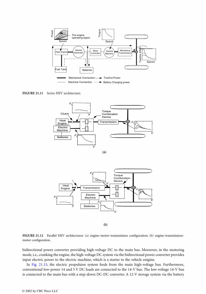
bidirectional power converter providing high-voltage DC to the main bus. Moreover, in the motoringmode, i.e., cranking the engine, the high-voltage DC system via the bidirectional power converter providesinput electric power to the electric machine, which is a starter to the vehicle enigine.
In Fig. 21.13, the electric propulsion system feeds from the main high-voltage bus. Furthermore,conventional low-power 14 and 5 V DC loads are connected to the 14-V bus. The low-voltage 14-V busis connected to the main bus with a step-down DC-DC converter. A 12-V storage system via the battery
FIGURE 21.11 Series HEV architecture.
FIGURE 21.12 Parallel HEV architectures: (a) engine–motor–transmission configuration; (b) engine–transmission–motor configuration.
Fuel Tank
Heat EngineElectric
Generator Electric
Machine
MechanicalTransmission
Batteries
Mechanical Connection
Electrical Connection
MotorController
Tractive Power
Battery Charging power
Speed
Pow
er
Speed
Tor
que
SpeedTra
ctiv
e E
ffort
The engine operating region
Transmission Heat
Engine
ElectricMachine
Batteries
Clutch TorqueCombinationDevice
V
V
V
(a)
Transmission Heat
Engine
ElectricMachine
Batteries
Torque CombinationDevice
V
V
Ft
Ft
Ft
Ft
Ft
Ft
Ft
V
V
(b)
© 2002 by CRC Press LLC
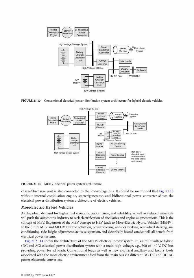
charge/discharge unit is also connected to the low-voltage bus. It should be mentioned that Fig. 21.13without internal combustion engine, starter/generator, and bidirectional power converter shows theelectrical power distribution system architecture of electric vehicles.
More-Electric Hybrid Vehicles
As described, demand for higher fuel economy, performance, and reliablility as well as reduced emissionswill push the automotive industry to seek electrification of ancillaries and engine augmentations. This is theconcept of MEV. Expansion of the MEV concept to HEV leads to More-Electric Hybrid Vehicles (MEHV).In the future MEV and MEHV, throttle actuation, power steering, antilock braking, rear-wheel steering, air-conditioning, ride-height adjustment, active suspension, and electrically heated catalyst will all benefit fromelectrical power systems.
Figure 21.14 shows the architecture of the MEHV electrical power system. It is a multivoltage hybrid(DC and AC) electrical power distribution system with a main high-voltage, e.g., 300 or 140 V, DC busproviding power for all loads. Conventional loads as well as new electrical ancillary and luxury loadsassociated with the more electric environment feed from the main bus via different DC-DC and DC-ACpower electronic converters.
FIGURE 21.13 Conventional electrical power distribution system architecture for hybrid electric vehicles.
FIGURE 21.14 MEHV electrical power system architecture.
© 2002 by CRC Press LLC

Automotive Electric Motor Drives
In a more electric car, most of the electrical loads, such as power steering and air-conditioning, requireefficient, fault-tolerant, robust, simple, and compact electric motors. Different electric machines andpower electronic converters will be used to facilitate conventional as well as advanced functions in futureautomotive systems.
DC motors with or without brushes are used for applications such as fans and pumps because of theirhigh efficiency in addition to reduced cost, flexible control, high quality, and reliablity. Induction and variablereluctance machines are candidates for starter/generator systems. The comparison of these two machinesfor automotive applications is based on the electromagnetic weight, power density, efficiency, controlcomplexity and features, complexity of design and fabrication, reliability, and thermal robustness [13, 14].
In EV and HEV, AC induction, DC commutator, and permanent magnet (PM) brushless DC motorsare commonly used for propulsion systems. Recently, there has also been interest in switched reluctancemotors (SRM) and synchronous reluctance motors [12, 15]. It is widely accepted that a suitable motordrive for traction applications in a vehicle should offer high efficiency, compactness, and low-cost manu-facturing among other attributes. It is also important to remember that a successful candidate mustprovide a fault-tolerant and hazard-free operation.
A review of past works shows that considerable attention has been paid to the development of high-efficiency motor drives whereas the impact of vehicle dynamics is neglected. A field-oriented PM motordrive can have a high effciency because of the free excitation. However, a limited extended-speed constant-power region along with poor performance in the presence of short circuits and high temperature mayprohibit effective use of these motor drives. Singly excited motor drives such as induction and switchedreluctance machines, on the other hand, seem to have an excellent performance in the presence of partialfailure and in harsh environments.
Conclusions
Advances in the areas of power electronics and electric motor drives along with fault-tolerant electricaldistribution systems and control electronics enable the transforming of present automotive power systemsinto MEV systems. The future electrical power system for conventional cars will most likely be a single-voltage bus (42 V DC) with provision for hybrid and multivoltage-level distribution. On the other hand,the clearest direction for future HEV electrical power systems is a multivoltage system providing powerfor traction load and other automotive loads via high-voltage, e.g., 300 or 140 V DC, and low-voltage,e.g., 42 and/or 14 V DC, buses, respectively. The extent of these changes will certainly depend on cost-effective production of power electronics and other automotive electric and electronic components.
References
1. J. M. Miller, A. Emadi, A. V. Rajarathnam, and M. Ehsani, Current status and future trends in moreelectric car power systems, in Proc. 1999 IEEE Vehicular Technology Conference, Houston, TX, May1999.
2. A. Emadi, M. Ehsani, and J. M. Miller, Advanced silicon rich automotive electrical power systems,presented at 18th Digital Avionics Systems Conference on Air, Space, and Ground Vehicle ElectronicSystems, St. Louis, MO, Oct. 1999.
3. J. G. Kassakian, H. C. Wolf, J. M. Miller, and C. J. Hurton, Automotive electrical systems-circa 2005,IEEE Spectrum, 22–27, Aug. 1996.
4. J. M. Miller, D. Goel, D. Kaminski, H. P. Schoner, and T. Jahns, Making the case for a next generationautomotive electrical system, presented at Convergence Transportation Electronics Association Con-gress, Dearborn, MI, Oct. 1998.
5. J. M. Miller and P. R. Nicastri, The next generation automotive electrical power system architecture:issues and challenges, presented at 17th Digital Avionics Systems Conference on Air, Space, andGround Vehicle Electronic Systems, Bellevue, WA, Oct./Nov. 1998.
© 2002 by CRC Press LLC

6. L. A. Khan, Automotive electrical systems: architecture and components, presented at 18th DigitalAvionics Systems Conference on Air, Space, and Ground Vehicle Electronic Systems, St. Louis, MO,Oct. 1999.
7. S. Muller and X. Pfab, Considerations implementing a dual voltage power network, presented atConvergence Transportation Electronics Association Congress, Dearborn, MI, Oct. 1998.
8. J. G. Kassakian, The future of power electronics in advanced automotive electrical systems, in Proc.IEEE Power Electronics Specialist Conf., 1996, 7–14.
9. C. C. Chan, An overview of electric vehicle technology, Proc. IEEE, 81(9), 1202–1213, 1993.10. C. C. Chan and K. T. Chau, An overview of power elecetronics in electric vehicles, IEEE Trans. Ind.
Electron. 44(1), 3–13, 1997.11. A. Emadi, B. Fahimi, M. Ehsani, and J. M. Miller, On the suitability of low-voltage (42 V) electrical
power system for traction applications in the parallel hybrid electric vehicles, Soc. Automotive Eng.(SAE) J., paper 2000-01-1558, 2000.
12. M. Ehsani, K. M. Rahman, and H. A. Toliyat, Propulsion system design of electric and hybrid vehicles,IEEE Trans. Ind. Electron., 44(1), 19–27, 1997.
13. J. M. Miller, P. J. McCleer, and J. H. Lang, Starter-alternator for hybrid electric vehicle: comparisonof induction and variable reluctance machines and drives, in Proc. 33rd IEEE Industry ApplicationSociety Annual Meeting, Oct. 1998, 513–523.
14. J. M. Miller, P. R. Nicastri, and S. Zarei, The automobile power supply in the 21st century, presentedat Power Systems World Conference and Exposition, Santa Clara, CA, Nov. 1998.
15. J. G. W. West, DC, induction, reluctance and PM motors for electric vehicles, Power Eng. J., 77–88,April 1994.
© 2002 by CRC Press LLC

22Principles of Magnetics
22.1 Introduction22.2 Nature of a Magnetic Field22.3 Electromagnetism22.4 Magnetic Flux Density22.5 Magnetic Circuits22.6 Magnetic Field Intensity22.7 Maxwell’s Equations22.8 Inductance22.9 Practical Considerations
22.1 Introduction
Although magnetism has been known since ancient times, the connection between electricity and mag-netism was not discovered until the early 19th century. Electromagnetics is the study of electric andmagnetic field behavior. These fields arise from charged particles both at rest and in motion, and theymay exert forces on other charged particles and materials.
Hans Christian Oersted (a Danish scientist) demonstrated the relation between electricity and mag-netism. In 1819, he showed that a compass needle could be deflected by a current-carrying conductor.Andrew Ampere (1775–1836) experimented with two current-carrying conductors and found that theyrepel or attract each other. He developed a concept to understand the electromagnetism that led to thedevelopment of transformers and electric generators.
The theory of electromagnetic fields was developed by James Clerk Maxwell (Scottish scientist) andpublished in 1865. His work was the culmination of a long series of experimental and theoretical researchperformed by a number of other scientists over the centuries. Maxwell published a set of equations thatcompletely describe the electromagnetic field. He developed a unified theory of electromagnetism, andhe also predicted the existence of radio waves. Heinrich Hertz (a German physicist) proved the existenceof such waves early in the 20th century.
The electromagnetic force (emf) is one of the four known fundamental forces of nature. The emf isresponsible for the functioning of a large number of devices that are important to modern civilizationincluding radio, television, cellular telephones, computers, and electric machinery. The emf is caused byan electromagnetic field that is described by two quantities, the electric field and the magnetic field, bothof which can vary in space and time.
22.2 Nature of a Magnetic Field
Magnetism can create a force between magnetic materials depending on their magnetic fields. Magneticfields can be produced by moving charged particles in electromagnets (e.g., electrons flowing through acoil of wire connected to a battery) or in permanent magnets (spinning electrons within the atomsgenerate the field). Figure 22.1 shows Faraday’s concept of the magnetic flux lines or lines of force on a
Roman StemprokUniversity of North Texas
© 2002 by CRC Press LLC
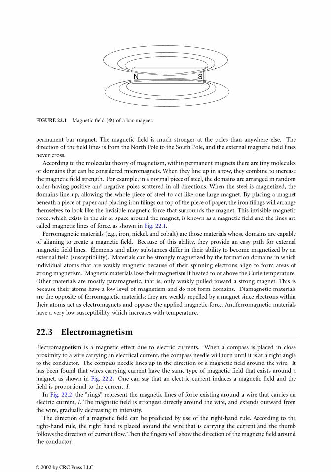
permanent bar magnet. The magnetic field is much stronger at the poles than anywhere else. Thedirection of the field lines is from the North Pole to the South Pole, and the external magnetic field linesnever cross.
According to the molecular theory of magnetism, within permanent magnets there are tiny moleculesor domains that can be considered micromagnets. When they line up in a row, they combine to increasethe magnetic field strength. For example, in a normal piece of steel, the domains are arranged in randomorder having positive and negative poles scattered in all directions. When the steel is magnetized, thedomains line up, allowing the whole piece of steel to act like one large magnet. By placing a magnetbeneath a piece of paper and placing iron filings on top of the piece of paper, the iron filings will arrangethemselves to look like the invisible magnetic force that surrounds the magnet. This invisible magneticforce, which exists in the air or space around the magnet, is known as a magnetic field and the lines arecalled magnetic lines of force, as shown in Fig. 22.1.
Ferromagnetic materials (e.g., iron, nickel, and cobalt) are those materials whose domains are capableof aligning to create a magnetic field. Because of this ability, they provide an easy path for externalmagnetic field lines. Elements and alloy substances differ in their ability to become magnetized by anexternal field (susceptibility). Materials can be strongly magnetized by the formation domains in whichindividual atoms that are weakly magnetic because of their spinning electrons align to form areas ofstrong magnetism. Magnetic materials lose their magnetism if heated to or above the Curie temperature.Other materials are mostly paramagnetic, that is, only weakly pulled toward a strong magnet. This isbecause their atoms have a low level of magnetism and do not form domains. Diamagnetic materialsare the opposite of ferromagnetic materials; they are weakly repelled by a magnet since electrons withintheir atoms act as electromagnets and oppose the applied magnetic force. Antiferromagnetic materialshave a very low susceptibility, which increases with temperature.
22.3 Electromagnetism
Electromagnetism is a magnetic effect due to electric currents. When a compass is placed in closeproximity to a wire carrying an electrical current, the compass needle will turn until it is at a right angleto the conductor. The compass needle lines up in the direction of a magnetic field around the wire. Ithas been found that wires carrying current have the same type of magnetic field that exists around amagnet, as shown in Fig. 22.2. One can say that an electric current induces a magnetic field and thefield is proportional to the current, I.
In Fig. 22.2, the “rings” represent the magnetic lines of force existing around a wire that carries anelectric current, I. The magnetic field is strongest directly around the wire, and extends outward fromthe wire, gradually decreasing in intensity.
The direction of a magnetic field can be predicted by use of the right-hand rule. According to theright-hand rule, the right hand is placed around the wire that is carrying the current and the thumbfollows the direction of current flow. Then the fingers will show the direction of the magnetic field aroundthe conductor.
FIGURE 22.1 Magnetic field (Φ) of a bar magnet.
N S
© 2002 by CRC Press LLC

Figure 22.3 shows a case where the wire is looped into a coil. A little magnetic field wraps aroundeach wire and, by combining each wire turn, the coil magnetic flux (Φ) is created. It was found byexperimentation that if a wire is wound in the form of a coil, the total magnetic field around the coil ismagnified. This is because the magnetic fields of the turns add up to make one large flux flow, resultingin a magnetic field (Φ), shown in Fig. 22.3.
22.4 Magnetic Flux Density
Fig. 22.4 shows a ferromagnetic material where the most of flux is combined to the core. Only a small amountof the leakage flux escapes on the sides of the coil. The unit of flux (Φ) is the weber in the SI system. Fluxdensity (B) is the magnetic flux per unit area. If the cross-sectional area (A) in SI units is m
2, then the flux
density is in webers per m2 (Wb/m
2), which is called tesla (T). Flux density (B) is defined by the total flux (Φ)
passing perpendicularly through an area (A).
(22.1)
22.5 Magnetic Circuits
Current (I) flowing through the coil shown in Figs. 22.3 and 22.4 creates the magnetomotive force ().The greater number of turns, the greater will be the flux. The magnetomotive force, or mmf, is defined as
(22.2)
where N is the number of coil turns and I is the current passing through the wire. For example, a coilwith 200 turns and 2 A will have an mmf of 400 At.
FIGURE 22.2 Magnetic field produced by current, I.
FIGURE 22.3 Magnetic field (Φ) produced by a coil.
ΦΦ
I
ISouth
NorthΦΦ
BΦA----= T( )
N · I ampere—turns, At( )=
© 2002 by CRC Press LLC

The magnitude of magnetic flux depends upon the opposition presented by the magnetic circuit. Theopposition to the flux is called reluctance, which is similar to resistance in an electric circuit. Thereluctance is defined as
(22.3)
where is the length of the magnetic core and A is a cross-sectional area. The property of the materialis characterized by its permeability, µ . Materials with high µ are called ferromagnetic materials, and thereluctance of those materials is low.
22.6 Magnetic Field Intensity
The magnetizing force, H, also known as magnetic field intensity, is the mmf per unit length. The magneticfield intensity is written as
(22.4)
Equation (22.4) describes an ability of a coil to produce magnetic flux. If, for example, in Fig. 22.4, thecoil has 1000 turns, the length of the magnetic path is 0.6 m and current through the conductor is 1 A,then the magnetic field intensity is 600 At/m.
The field intensity and the resulting flux density are related through the permeability. The flux density is
(22.5)
where µ is core permeability. The core permeability is a material constant describing the level of the fluxin a material. When the material constant (µ) is high, the flux density will increase. The permeabilityhas units of webers per ampere-turn-meter in the SI system. The permeability of vacuum in free spaceis µo = 4π × 10
−7 (Wb/At-m). When magnetic flux propagates through magnetic media, other than
vacuum, the flux density is
(22.6)
where µr is the relative permeability. The relative permeability is 1 for a vacuum and can reach 10,000for ferromagnetic materials. Ferromagnetic materials have regions called domains of microscopic size.
FIGURE 22.4 Magnetic flux density in a ferromagnetic material.
CoreFlux
IA
SmallLeakageFlux
Φ
mA------- At/Wb( )=
H---- NI
------ At/m( )= =
B mH T( )=
B mrmoH T( )=
© 2002 by CRC Press LLC

When they line up, the material is magnetized. Thus, one can increase the magnetic field until all domainsare aligned, at which point the ferromagnetic material is incapable of contributing any more magneticflux. At that point the material is saturated, as shown on the hysteresis curve in Fig. 22.5.
22.7 Maxwell’s Equations
Maxwell’s equations are the fundamental concept of electromagnetic (E-M) field theory. Using E-M fieldtheory, one can calculate important quantities such as impedance, inductance, capacitance, etc. Maxwell’sequations in differential form are as follows:
(22.7)
(22.8)
(22.9)
(22.10)
where H is the magnetic field intensity (A/m), D is the electric flux density (C/m2), B is the magnetic
flux density (T), J is the current density (A/m2), ρ is the charge density (C/m
3), and E is the electric field
intensity (V/m). The other relations to Maxwell’s equations are
(22.11)
(22.12)
(22.13)
where εo is the permittivity of free space (8.854 × 10⁻¹²
F/m) and εr is the relative dielectric constant fora given material. In the second equation, µo is the permeability of free space (4π × 10
−7) and µr is the
relative permeability for a given material. In the third equation, σ is the electric conductivity (Siemens).
FIGURE 22.5 Hysteresis loop.
B
H
ResidualMagnetism
Saturation
slope = µ = B/Ho
∇ H× J∂D∂t-------+=
∇ E× ∂B∂t------–=
∇ · D r=
∇ · B 0=
D eE er eo E= =
B mH mr mo H= =
J s E=
© 2002 by CRC Press LLC

Maxwell’s equations can be rewritten into integral form using mathematical tools, such as Stokes’theorem and the divergence theorem, and then they look as follows:
Faraday’s law: (22.14)
Ampere’s law: (22.15)
Gauss’ law: (22.16)
(22.17)
Michael Faraday (1791–1867) experimented with magnetic fields. He wound two coils on an iron ring.When one coil was powered from a battery, he noticed that a transient voltage developed on the secondcoil and, later, this led him to develop a transformer. Faraday concluded from his observations thatvoltage is induced in a circuit whenever the linking flux in the magnetic circuit changes. He alsodiscovered a formula describing the change of a magnetic flux, which is proportional to the voltagechange across the coil. Equation (22.14) shows the Faraday law in the integral form derived from Maxwell’sequations. The first right-hand term of this equation is regular current flowing in a wire, and the secondterm is due to capacitive coupling called the “displacement current.” In most cases the displacementcurrent is neglected.
An example of a magnetic field density at a distance r of a long straight wire is shown in Fig. 22.6.One can assume I = 100 A, r = 1 m, and µ = µo. Using Eq. (22.14) one can write
and take the integral around the wire at a constant distance r.Integrating over a circular path,
and then,
FIGURE 22.6 Long straight wire carrying a current, I.
H · d∫° I∂D∂t------- · ds
s∫+=
E · d∫°∂B∂t------ · ds
s∫–=
D · dss∫° qencl. r vd
vol∫= =
B · dss∫° qencl. 0= =
∫° H · d I=
H · d∫° 2prHΦ I= =
BΦmI
2pr--------- 100 4p 10 7–××
2p 1×------------------------------------- 2 10 5–× T( )= = =
© 2002 by CRC Press LLC

In this example magnetic field lines form circles around the wire, as shown in Fig. 22.2. The magneticfield intensity decreases with distance from the wire.
By Faraday’s law, the induced voltage is proportional to the rate of the magnetic flux change times thenumber of turns in a coil. In calculus notation, the rate of flux change times the number of turns is
(22.18)
where e is in volts, Φ is webers, N is the number of turns, and t is in seconds. For example, if the magneticflux changes at a rate of 1 Wb/s in a single turn coil, the induced voltage is 1 V.
22.8 Inductance
The induced voltage in a coil is proportional to the magnetic flux change that is shown in Eq. (22.18).It is also known that the induced current is proportional to the current. Thus, one can write that theinduced voltage is proportional to the current change,
(22.19)
where L is the inductance of the coil. The unit of inductance is the henry in the SI system. In practice,in electrical circuit calculations, the voltage across the inductance is denoted by vL rather than e. Then,one can rewrite Eq. (22.19) as
(22.20)
22.9 Practical Considerations
Faraday’s law states that a time-varying magnetic field through a surface bounded by a closed path inducesa voltage inside a conductor loop. This fundamental principle has important consequences for parasiticcoupling in electronic hardware, such as a noisy circuit on a printed circuit board of a computer. Theproblem is a significant time-varying magnetic field as a result of current levels in different conductivetraces. Some of the traces can make current loops. The magnetic field generated by the loop area “looks”for other loops—the circuits where it can induce a voltage across the load. We consider the target looparea when looking at its mutual inductance, and the target loop area is determined by the closed currentpath in the victim circuit. The magnitude of induced voltage in the victim circuit depends on variousfactors:
• Current magnitude in the first circuit
• Source and load circuit impedances
• Size of the loop area in the victim circuit
• Distance between the victim and source circuits
• Orientation of the loops
This coupling can cause faulty operation of the victim circuit.
e NdΦdt------- V( )=
e Ldidt----- V( )=
vL Ldidt----- V( )=
© 2002 by CRC Press LLC