Embed Size (px)
Citation preview

The Physics of Superconducting Microwave Resonators
Thesis by
Jiansong Gao
In Partial Fulfillment of the Requirements
for the Degree of
Doctor of Philosophy
California Institute of Technology
Pasadena, California
2008
(Defended May 28, 2008)

ii
c© 2008
Jiansong Gao
All Rights Reserved

iii
This thesis is dedicated to my dearest wife, Yingyan, who has been a constant source of inspiration
and support through all stages of my life since high school, and to our lovely boy, Logan, who came
to our family just before the thesis was finished.

iv
Acknowledgments
First, I would like to thank my advisor Professor Jonas Zmuidzinas for giving me the opportunity
to work on this great project of MKID. I came to Caltech in 2002 and originally planned to work
in the field of optics. Failing to join any optics group on campus, I luckily ran across Jonas in a
talk on MKID he gave to the students in applied physics major. These detectors made of resonators
immediately attracted my interest. I still remember the interview that took place at Jonas’ office.
Desperate to join a research group, I was advertising how good I was in both theory and experiment.
At some point I mentioned that I had taken a mathematical course on stochastic process, which had
caught Jonas’ attention. He immediately gave me a quiz, asking me to state the Weiner-Kinchin
theorem. Fortunately, I was able to give the correct answer promptly. He was very satisfied and
said, “Let me show you the lab.”
That was how I joined the MKID group and also where my journey of noise study started. It
turns out that in the past five years, there wasn’t a single day in which I wasn’t dealing with the
noise spectrum, stochastic process or the Weiner-Kinchin theorem. And of course, I enjoyed it very
much. Noise in superconducting microwave resonators is a problem that has never been studied
before. It is challenging but equally fascinating. Jonas has given me enough freedom in tackling the
problem, as well as critical advice in times I could not find my way out. Every discussion with him
boosted my knowledge, deepened my understanding and led to small or big progress in my research.
I also enjoy and benefit a lot from the collaboration with a group of great people. The cryostat
and the measurement setup are all taken care of by Dr. Ben Mazin. This has saved me a huge
amount of time on the hardware which I’m not good at. Also, as the first student on MKID project,
his thesis is the starting point of my work and in some sense I am harvesting the fruits of his previous
hard work. Thanks to the fact that an international student has no easy access to JPL. So I don’t
have to worry about the fabrication at all – Dr. Rick LeDuc at the microdevice lab in JPL will
always turn my drawings into the best made devices. Some other devices are supplied by Miguel
Daal, my collaborator and also my best friend from UC Berkeley. His devices appear to be more
noisy than Rick’s devices, which may be a bad thing for a detector but not bad for me, who study
noise on purpose, at all. It turns out his devices has led to some of the most important progress.
We also spent a lot of afternoons in front of Red Door Cafe, talking about ideas that were too crazy

v
or too stupid to be discussed with professors. Dr. Peter Day from JPL supervised me in the year
when Jonas was ill. He has given me a lot of guidance both on theory and experiment, as well as
on paper writing. Anastasios Vayonakis taught me a lot of things, from how to use a wire bonder
to how to repair a car. Asking him about microwave engineering and cryogenic instrumentation
has always been an shortcut for me to solve practical problems in these areas. I would like to give
special thanks to Prof. John Martinis form UC Santa Babara, who is very enthusiastic on the noise
problem I am working on. Some of my work was inspired by his paper and discussions with him.
Professor Sunil Golowala and Bernald Sadoulet, graduate students Megan Eckart, Shwetank Kumar,
James Schlaerth, Omid Noroozian and David Moore have all given me many help and support to
this thesis work.
I would also like to thank my parents, my sister and members in my extended family for their
remote love and support.
Funding for this project has been provided by NASA, JPL DRDF, and the generous contributions
of Alex Lidow, Caltech Trustee.

vi
Abstract
Over the past decade, low temperature detectors have been of great interest to the astronomy
community. These detectors work at very low temperatures, usually well below 1 K. Their ultra-high
sensitivity has brought astronomers revolutionary new observational capabilities and led to many
great discoveries, such as the demonstration that the geometry of the universe is flat[1, 2]. Although a
single low temperature detector has very impressive sensitivity, a large array of them would be much
more powerful and are highly demanded for the study of more difficult and fundamental problems
in astronomy. However, current detector technologies, such as transition edge sensors (TESs) and
superconducting tunnel junction (STJ) detectors, are difficult to integrate into a large array. When
the pixel count becomes relatively large (> 1000), great technical challenges are encountered in
fabricating and in reading out these detectors.
The microwave kinetic inductance detector (MKID) is a promising new detector technology
invented at Caltech and JPL which provides both high sensitivity and an easy solution to the
integration of detectors into a large array. It operates on the principle that the surface impedance
of a superconductor changes as incoming photons break Cooper pairs. This change is read out
by using high-Q superconducting microwave resonators capacitively coupled to a common feedline.
This architecture allows thousands of detectors (resonators) to be easily integrated through passive
frequency domain multiplexing. In addition, MKIDs are easy to fabricate and require minimal
cryogenic electronics support (a single HEMT amplifier can potentially multiplex 103−104 MKIDs).
In this thesis we will explore the rich and interesting physics behind these superconducting
microwave resonators used in MKIDs. This study was carried out around two main topics, the
responsivity and the noise of MKIDs.
In the discussion of the responsivity, the following physics are visited:
1. How does the surface impedance of a superconductor change with quasiparticle density?
2. What fraction of the distributed inductance of a superconducting transmission line is
contributed by the superconductor?
3. What is the static and dynamic response of the microwave resonant circuit used in MKIDs?
The first question is answered in Chapter 2 by applying the Mattis-Bardeen theory to bulk and
thin-film superconductors. The second question is answered in Chapter 3 by solving the quasi-TEM

vii
mode of the coplanar wave guide (CPW) using the tool of conformal mapping. The third question
is answered in Chapter 4 by applying the network theory to the readout circuit.
The experimental study of the noise is presented in Chapter 5, which is the focus of this thesis.
Before noise was measured on the first MKID, the fundamental noise limit was understood to be the
quasi-particle generation-recombination noise. Unexpectedly, a significant amount of excess noise
was observed. From a large number of experiments, we have found this excess noise to be pure
frequency noise (equivalent to a jitter in the resonance frequency), with the noise level depending on
the microwave power, the bath temperature, the superconductor/substrate materials combination,
and the geometry of the resonator. The observed noise properties suggest that the excess noise is
not related to the superconductor but is caused by the two-level systems (TLS) in the dielectric
materials in the resonator. The TLS are tunneling states which exist in amorphous solids and
causes the anomalous properties of these solids at low temperatures. Several special experiments
were designed to test the TLS hypothesis. From these experiments, we find that the effects of the
TLS on the resonance frequency and the quality factor of the resonators are in good agreement with
the TLS theory. In an important experiment we explored the geometrical scaling of TLS-induced
frequency shift and noise. The results give direct experimental evidence that the TLS, responsible
for the low temperature resonance frequency shift, dissipation, and frequency noise, are distributed
on the surface of the resonator, but not in the bulk substrate. Guided by the measured noise scaling
with geometry and power, we have come up with a semi-empirical noise model which assumes a
surface distribution of independent TLS fluctuators. With this knowledge about TLS and excess
noise, we propose a number of methods that can potentially reduce the excess noise.
Parallel to the experimental study, we have also taken great effort in working toward a theoretical
model of the noise. It is likely that the noise is related to the dielectric constant fluctuation caused by
the state switching (by absorption or emission of thermal phonons) or the energy level fluctuations
of the TLS. However, at the time this thesis was finished, we still do not have a complete theory
that can quantitatively explain all the experimental observations, and therefore the detailed physical
noise mechanism is still not clear.
With the theoretical results of the responsivity and the semi-empirical model of the noise es-
tablished in this thesis, a prediction of the detector sensitivity (noise equivalent power) and an
optimization of MKID design are now possible, which was the original motivation of this thesis.

viii
Contents
Acknowledgments iv
Abstract vi
List of Figures xiv
List of Tables xvii
1 Introduction 1
1.1 Microwave kinetic inductance detectors . . . . . . . . . . . . . . . . . . . . . . . . . 1
1.1.1 Introduction to low temperature detectors . . . . . . . . . . . . . . . . . . . . 1
1.1.2 Principle of operation . . . . . . . . . . . . . . . . . . . . . . . . . . . . . . . 2
1.1.3 Technical advantages . . . . . . . . . . . . . . . . . . . . . . . . . . . . . . . . 4
1.1.4 Applications and ongoing projects . . . . . . . . . . . . . . . . . . . . . . . . 5
1.1.4.1 Antenna-coupled MKIDs for millimeter and submillimeter imaging . 5
1.1.4.2 MKID strip detectors for optical/X-ray . . . . . . . . . . . . . . . . 6
1.1.4.3 MKID phonon sensor for dark matter search . . . . . . . . . . . . . 7
1.2 Other applications of superconducting microwave resonators . . . . . . . . . . . . . . 9
1.2.1 Microwave frequency domain multiplexing of SQUIDs . . . . . . . . . . . . . 9
1.2.2 Coupling superconducting qubits to microwave resonators . . . . . . . . . . . 10
1.2.3 Coupling nanomechanical resonators to microwave resonators . . . . . . . . . 11
2 Surface impedance of superconductor 13
2.1 Non-local electrodynamics of superconductor and the Mattis-Bardeen theory . . . . 13
2.2 Surface impedance of bulk superconductor . . . . . . . . . . . . . . . . . . . . . . . . 16
2.2.1 Solution of the Mattis-Bardeen kernel K(q) . . . . . . . . . . . . . . . . . . . 16
2.2.2 Asymptotic behavior of K(q) . . . . . . . . . . . . . . . . . . . . . . . . . . . 17
2.2.2.1 K(q → 0) . . . . . . . . . . . . . . . . . . . . . . . . . . . . . . . . . 18
2.2.2.2 K(q → ∞) . . . . . . . . . . . . . . . . . . . . . . . . . . . . . . . . 18
2.2.2.3 A sketch of K(q) . . . . . . . . . . . . . . . . . . . . . . . . . . . . . 19

ix
2.2.3 Surface impedance Zs and effective penetration depth λeff for specular and
diffusive surface scattering . . . . . . . . . . . . . . . . . . . . . . . . . . . . . 19
2.2.4 Surface impedance in two limits . . . . . . . . . . . . . . . . . . . . . . . . . 21
2.2.4.1 Extreme anomalous limit . . . . . . . . . . . . . . . . . . . . . . . . 22
2.2.4.2 Local limit . . . . . . . . . . . . . . . . . . . . . . . . . . . . . . . . 23
2.2.5 Numerical approach . . . . . . . . . . . . . . . . . . . . . . . . . . . . . . . . 24
2.2.6 Numerical results . . . . . . . . . . . . . . . . . . . . . . . . . . . . . . . . . . 24
2.2.6.1 λeff of Al and Nb at zero temperature . . . . . . . . . . . . . . . . . 24
2.2.6.2 Temperature dependence of Zs . . . . . . . . . . . . . . . . . . . . . 25
2.2.6.3 Frequency dependence of Zs . . . . . . . . . . . . . . . . . . . . . . 27
2.3 Surface impedance of superconducting thin films . . . . . . . . . . . . . . . . . . . . 27
2.3.1 Equations for specular and diffusive surface scattering . . . . . . . . . . . . . 27
2.3.2 Numerical approach . . . . . . . . . . . . . . . . . . . . . . . . . . . . . . . . 29
2.3.2.1 Implementing the finite difference method . . . . . . . . . . . . . . . 29
2.3.2.2 Boundary condition . . . . . . . . . . . . . . . . . . . . . . . . . . . 30
2.3.2.3 Retrieving the results . . . . . . . . . . . . . . . . . . . . . . . . . . 30
2.3.3 Numerical results . . . . . . . . . . . . . . . . . . . . . . . . . . . . . . . . . . 31
2.3.3.1 λeff of Al thin film . . . . . . . . . . . . . . . . . . . . . . . . . . . . 31
2.4 Complex conductivity σ = σ1 − jσ2 . . . . . . . . . . . . . . . . . . . . . . . . . . . . 32
2.4.1 Surface impedance Zs in various limits expressed by σ1 and σ2 . . . . . . . . 33
2.4.1.1 Thick film, extreme anomalous limit . . . . . . . . . . . . . . . . . . 33
2.4.1.2 Thick film, local limit . . . . . . . . . . . . . . . . . . . . . . . . . . 33
2.4.1.3 Thin film . . . . . . . . . . . . . . . . . . . . . . . . . . . . . . . . . 34
2.4.2 Change in the complex conductivity δσ due to temperature change and pair
breaking . . . . . . . . . . . . . . . . . . . . . . . . . . . . . . . . . . . . . . . 34
2.4.2.1 Relating δZs to δσ . . . . . . . . . . . . . . . . . . . . . . . . . . . . 34
2.4.2.2 Effective chemical potential µ∗ . . . . . . . . . . . . . . . . . . . . . 34
2.4.2.3 Approximate formulas of ∆, nqp, σ, and dσ/dnqp for both cases . . 36
2.4.2.4 Equivalence between thermal quasiparticles and excess quasiparticles
from pair breaking . . . . . . . . . . . . . . . . . . . . . . . . . . . 37
3 Kinetic inductance fraction of superconducting CPW 39
3.1 Theoretical calculation of α from quasi-static analysis and conformal mapping technique 39
3.1.1 Quasi-TEM mode of CPW . . . . . . . . . . . . . . . . . . . . . . . . . . . . 40
3.1.2 Calculation of geometric capacitance and inductance of CPW using conformal
mapping technique . . . . . . . . . . . . . . . . . . . . . . . . . . . . . . . . . 43

x
3.1.2.1 Zero thickness . . . . . . . . . . . . . . . . . . . . . . . . . . . . . . 44
3.1.2.2 Finite thickness with t≪ a . . . . . . . . . . . . . . . . . . . . . . . 46
3.1.2.3 General case of finite thickness from a numerical approach . . . . . 48
3.1.2.4 Results of L and C calculated using different methods . . . . . . . . 50
3.1.3 Theoretical calculation of α for thick films (t ≫ λeff) . . . . . . . . . . . . . . 50
3.1.3.1 Kinetic inductance Lki, kinetic inductance fraction α, and geometri-
cal factor g . . . . . . . . . . . . . . . . . . . . . . . . . . . . . . . . 50
3.1.3.2 Approximate formula of g under the condition of t≪ a . . . . . . . 52
3.1.3.3 Numerical calculation of g for general cases . . . . . . . . . . . . . . 53
3.1.3.4 A comparison of g calculated using different methods . . . . . . . . 54
3.1.4 Theoretical calculation of α for thin films (t < λeff) . . . . . . . . . . . . . . . 54
3.1.5 Partial kinetic inductance fraction . . . . . . . . . . . . . . . . . . . . . . . . 56
3.2 Experimental determination of α . . . . . . . . . . . . . . . . . . . . . . . . . . . . . 58
3.2.1 Principle of the experiment . . . . . . . . . . . . . . . . . . . . . . . . . . . . 58
3.2.2 α-test device and the experimental setup . . . . . . . . . . . . . . . . . . . . 59
3.2.3 Results of 200 nm Al α-test device (t≫ λeff and t≪ a) . . . . . . . . . . . . 60
3.2.3.1 α of the smallest geometry . . . . . . . . . . . . . . . . . . . . . . . 60
3.2.3.2 Retrieving values of α from fr(T ) and Qr(T ) . . . . . . . . . . . . . 60
3.2.3.3 Comparing with the theoretical calculations . . . . . . . . . . . . . 62
3.2.4 Results of 20 nm Al α-test device (t < λeff) . . . . . . . . . . . . . . . . . . . 63
3.2.4.1 α of the smallest geometry . . . . . . . . . . . . . . . . . . . . . . . 63
3.2.4.2 Retrieving values of α from fr(T ) . . . . . . . . . . . . . . . . . . . 63
3.2.4.3 Comparing with the theoretical calculations . . . . . . . . . . . . . 64
3.2.5 A table of experimentally determined α for different geometries and thicknesses. 64
4 Analysis of the resonator readout circuit 66
4.1 Quarter-wave transmission line resonator . . . . . . . . . . . . . . . . . . . . . . . . 66
4.1.1 Input impedance and equivalent lumped element circuit . . . . . . . . . . . . 66
4.1.2 Voltage, current, and energy in the resonator . . . . . . . . . . . . . . . . . . 68
4.2 Network model of a quarter-wave resonator capacitively coupled to a feedline . . . . 69
4.2.1 Network diagram . . . . . . . . . . . . . . . . . . . . . . . . . . . . . . . . . . 70
4.2.2 Scattering matrix elements of the coupler’s 3-port network . . . . . . . . . . . 70
4.2.3 Scattering matrix elements of the extended coupler-resonator’s 3-port network 71
4.2.4 Transmission coefficient t21 of the reduced 2-port network . . . . . . . . . . . 71
4.2.5 Properties of the resonance curves . . . . . . . . . . . . . . . . . . . . . . . . 73
4.3 Responsivity of MKIDs I — shorted λ/4 resonator (Zl = 0) . . . . . . . . . . . . . . 75

xi
4.4 Responsivity of MKIDs II — λ/4 resonator with load impedance (Zl 6= 0) . . . . . . 77
4.4.1 Hybrid resonators . . . . . . . . . . . . . . . . . . . . . . . . . . . . . . . . . 77
4.4.2 Static response . . . . . . . . . . . . . . . . . . . . . . . . . . . . . . . . . . . 78
4.4.3 Power dissipation in the sensor strip . . . . . . . . . . . . . . . . . . . . . . . 79
4.4.4 Dynamic response . . . . . . . . . . . . . . . . . . . . . . . . . . . . . . . . . 79
5 Excess noise in superconducting microwave resonators 83
5.1 A historical overview of the noise study . . . . . . . . . . . . . . . . . . . . . . . . . 83
5.2 Noise measurement and data analysis . . . . . . . . . . . . . . . . . . . . . . . . . . 85
5.3 General properties of the excess noise . . . . . . . . . . . . . . . . . . . . . . . . . . 88
5.3.1 Pure phase (frequency) noise . . . . . . . . . . . . . . . . . . . . . . . . . . . 88
5.3.2 Power dependence . . . . . . . . . . . . . . . . . . . . . . . . . . . . . . . . . 90
5.3.3 Metal-substrate dependence . . . . . . . . . . . . . . . . . . . . . . . . . . . . 91
5.3.4 Temperature dependence . . . . . . . . . . . . . . . . . . . . . . . . . . . . . 92
5.3.5 Geometry dependence . . . . . . . . . . . . . . . . . . . . . . . . . . . . . . . 94
5.4 Two-level system model . . . . . . . . . . . . . . . . . . . . . . . . . . . . . . . . . . 95
5.4.1 Tunneling states . . . . . . . . . . . . . . . . . . . . . . . . . . . . . . . . . . 95
5.4.2 Two-level dynamics and the Bloch equations . . . . . . . . . . . . . . . . . . 97
5.4.3 Solution to the Bloch equations . . . . . . . . . . . . . . . . . . . . . . . . . . 99
5.4.4 Relaxation time T1 and T2 . . . . . . . . . . . . . . . . . . . . . . . . . . . . . 100
5.4.5 Dielectric properties under weak and strong electric fields . . . . . . . . . . . 102
5.4.5.1 Weak field . . . . . . . . . . . . . . . . . . . . . . . . . . . . . . . . 103
5.4.5.2 Strong field . . . . . . . . . . . . . . . . . . . . . . . . . . . . . . . . 104
5.4.6 A semi-empirical noise model assuming independent surface TLS fluctuators 106
5.5 Experimental study of TLS in superconducting resonators . . . . . . . . . . . . . . . 109
5.5.1 Study of dielectric properties and noise due to TLS using superconducting
resonators . . . . . . . . . . . . . . . . . . . . . . . . . . . . . . . . . . . . . 109
5.5.1.1 Sillicon nitride (SiNx) covered Al on sapphire device . . . . . . . . . 109
5.5.1.2 Nb microstrip with SiO2 dielectric on sapphire substrate . . . . . . 115
5.5.2 Locating the TLS noise source . . . . . . . . . . . . . . . . . . . . . . . . . . 119
5.5.2.1 Evidence for a surface distribution of TLS from frequency shift mea-
surement . . . . . . . . . . . . . . . . . . . . . . . . . . . . . . . . . 119
5.5.2.2 More on the geometrical scaling of frequency noise . . . . . . . . . . 123
5.6 Method to reduce the noise . . . . . . . . . . . . . . . . . . . . . . . . . . . . . . . . 126
5.6.1 Hybrid geometry . . . . . . . . . . . . . . . . . . . . . . . . . . . . . . . . . . 126
5.6.1.1 Two-section CPW . . . . . . . . . . . . . . . . . . . . . . . . . . . . 126

xii
5.6.1.2 A design using interdigitated capacitor . . . . . . . . . . . . . . . . 128
5.6.2 Removing TLS . . . . . . . . . . . . . . . . . . . . . . . . . . . . . . . . . . . 128
5.6.2.1 Coating with non-oxidizing metal . . . . . . . . . . . . . . . . . . . 128
5.6.2.2 Silicides . . . . . . . . . . . . . . . . . . . . . . . . . . . . . . . . . . 128
5.6.3 Amplitude readout . . . . . . . . . . . . . . . . . . . . . . . . . . . . . . . . . 129
6 Sensitivity of submm kinetic inductance detector 131
6.1 The signal chain and the noise propagation . . . . . . . . . . . . . . . . . . . . . . . 131
6.1.1 Quasiparticle density fluctuations δnqp under an optical loading p . . . . . . 132
6.1.1.1 Quasiparticle recombination r(t) . . . . . . . . . . . . . . . . . . . . 132
6.1.1.2 Thermal quasiparticle generation gth(t) . . . . . . . . . . . . . . . . 133
6.1.1.3 Excess quasiparticle generation gex(t) under optical loading . . . . 133
6.1.1.4 Steady state quasiparticle density nqp . . . . . . . . . . . . . . . . . 134
6.1.1.5 Fluctuations in quasiparticle density δnqp . . . . . . . . . . . . . . . 135
6.2 Noise equivalent power (NEP) . . . . . . . . . . . . . . . . . . . . . . . . . . . . . . . 136
6.2.1 Background loading limited NEP . . . . . . . . . . . . . . . . . . . . . . . . . 136
6.2.2 Detector NEP limited by the HEMT amplifier . . . . . . . . . . . . . . . . . 137
6.2.3 Requirement for the HEMT noise temperature Tn in order to achieve BLIP
detection . . . . . . . . . . . . . . . . . . . . . . . . . . . . . . . . . . . . . . 138
6.2.4 Detector NEP limited by the TLS noise . . . . . . . . . . . . . . . . . . . . . 139
A Several integrals encountered in the derivation of the Mattis-Bardeen kernel K(q)
and K(η) 142
A.1 Derivation of one-dimensional Mattis-Bardeen kernel K(η) and K(q) . . . . . . . . . 142
A.2 R(a, b) and S(a, b) . . . . . . . . . . . . . . . . . . . . . . . . . . . . . . . . . . . . 144
A.3 RR(a, b), SS(a, b), RRR(a, b, t), and SSS(a, b, t) . . . . . . . . . . . . . . . . . . 145
B Numerical tactics used in the calculation of surface impedance of bulk and thin-
film superconductors 147
B.1 Dimensionless formula . . . . . . . . . . . . . . . . . . . . . . . . . . . . . . . . . . . 147
B.2 Singularity removal . . . . . . . . . . . . . . . . . . . . . . . . . . . . . . . . . . . . . 148
B.3 Evaluation of K(η) . . . . . . . . . . . . . . . . . . . . . . . . . . . . . . . . . . . . . 149
C jt/jz in quasi-TEM mode 150
D Solution of the conformal mapping parameters in the case of t≪ a 152
xiii
E Fitting the resonance parameters from the complex t21 data 155
E.1 The fitting model . . . . . . . . . . . . . . . . . . . . . . . . . . . . . . . . . . . . . . 155
E.2 The fitting procedures . . . . . . . . . . . . . . . . . . . . . . . . . . . . . . . . . . . 155
E.2.1 Step 1: Removing the cable delay term . . . . . . . . . . . . . . . . . . . . . 156
E.2.2 Step 2: Circle fit . . . . . . . . . . . . . . . . . . . . . . . . . . . . . . . . . . 156
E.2.3 Step 3: Rotating and translating to the origin . . . . . . . . . . . . . . . . . . 158
E.2.4 Step 4: Phase angle fit . . . . . . . . . . . . . . . . . . . . . . . . . . . . . . . 158
E.2.5 Step 5: Retrieving other parameters . . . . . . . . . . . . . . . . . . . . . . . 159
E.3 Fine-tuning the fitting parameters . . . . . . . . . . . . . . . . . . . . . . . . . . . . 159
E.4 Fitting |t21|2 to the skewed Lorentzian profile . . . . . . . . . . . . . . . . . . . . . . 161
F Calibration of IQ-mixer and data correction 162
G Several integrals encountered in the calculation of ǫTLS(ω) 166
G.1 Integrating
χ res (ω) over TLS parameter space . . . . . . . . . . . . . . . . . . . . . 166
G.2 ǫTLS(ω) for weak field (| ~E| → 0). . . . . . . . . . . . . . . . . . . . . . . . . . . . . . 168
G.3 ǫTLS(ω) for nonzero ~E field. . . . . . . . . . . . . . . . . . . . . . . . . . . . . . . . . 169
H Semi-empirical frequency noise formula for a transmission line resonator 172
Bibliography 174

xiv
List of Figures
1.1 Principle of operation of MKID . . . . . . . . . . . . . . . . . . . . . . . . . . . . . . . 3
1.2 Pixel design of the antenna-coupled submm MKIDs . . . . . . . . . . . . . . . . . . . 6
1.3 MKID strip detectors for optical/X-ray . . . . . . . . . . . . . . . . . . . . . . . . . . 7
1.4 Scheme of a dark matter MKID using CPW resonators . . . . . . . . . . . . . . . . . 8
1.5 Scheme of a dark matter MKID using air-gapped microstrip resonators . . . . . . . . 9
1.6 Schematic of SQUID multiplexer . . . . . . . . . . . . . . . . . . . . . . . . . . . . . . 10
1.7 Integrated circuit for cavity QED . . . . . . . . . . . . . . . . . . . . . . . . . . . . . . 10
1.8 Device in which a nanomechanical resonator is coupled to a microwave resonator . . . 11
2.1 Configuration of a plane wave incident onto a bulk superconductor . . . . . . . . . . . 16
2.2 A sketch of K(q) . . . . . . . . . . . . . . . . . . . . . . . . . . . . . . . . . . . . . . . 19
2.3 The temperature dependence of the surface impedance of Al . . . . . . . . . . . . . . 25
2.4 δfr
frand δ 1
Qras a function of temperature . . . . . . . . . . . . . . . . . . . . . . . . . 26
2.5 Frequency dependance of effective penetration depth λeff of Al bulk superconductor. . 27
2.6 Configuration of a plane wave incident onto a superconducting thin film . . . . . . . . 28
2.7 Field configuration used by Sridhar to calculate Zs of a thin film . . . . . . . . . . . . 28
2.8 A thin film divided into N slices . . . . . . . . . . . . . . . . . . . . . . . . . . . . . . 29
2.9 Effective penetration depth λeff of Al thin film as a function of the film thickness d . . 32
2.10 dσ/dnqp vs. T calculated for thermal and external quasiparticles . . . . . . . . . . . . 37
3.1 Coplanar waveguide geometry . . . . . . . . . . . . . . . . . . . . . . . . . . . . . . . 40
3.2 Schwarz-Christoffel mapping . . . . . . . . . . . . . . . . . . . . . . . . . . . . . . . . 43
3.3 SC-mapping of a zero-thickness CPW into a parallel-plate capacitor . . . . . . . . . . 44
3.4 SC-mapping of a finite-thickness CPW into a parallel plate capacitor . . . . . . . . . . 46
3.5 Constructing the capacitance of a CPW with thickness t . . . . . . . . . . . . . . . . 47
3.6 Mapping a quadrant of a finite-thickness CPW into a rectangle . . . . . . . . . . . . . 48
3.7 Calculation of the exact capacitance of a CPW . . . . . . . . . . . . . . . . . . . . . . 49
3.8 ~E and ~H fields near the surface of a bulk superconducting CPW . . . . . . . . . . . . 51
3.9 Total inductance L as a function of the surface inductance Ls for a thin-film CPW . . 55

xv
3.10 Coupler structure of the α-test device. . . . . . . . . . . . . . . . . . . . . . . . . . . . 58
3.11 Measured δfr/fr and δ(1/Qr) as a function of T from the 200 nm α-test device . . . 61
3.12 δfr/fr normalized by group 1 from the 200 nm α-test device . . . . . . . . . . . . . . 61
3.13 Fitting δfr/fr and δ(1/Qr) data to the Mattis-Bardeen theory . . . . . . . . . . . . . 62
3.14 Measured δfr/fr as a function of T from the 20 nm α-test device . . . . . . . . . . . . 63
3.15 δfr/fr normalized by group-1 from the 20 nm α-test device . . . . . . . . . . . . . . . 63
3.16 Fitting δfr/fr data to the Mattis-Bardeen theory . . . . . . . . . . . . . . . . . . . . 64
4.1 A short-circuited λ/4 transmission line and its equivalent circuit . . . . . . . . . . . . 67
4.2 Network model of a λ/4 resonator capacitively coupled to a feedline . . . . . . . . . . 69
4.3 Plot of t21(f) and its variation t′21(f) . . . . . . . . . . . . . . . . . . . . . . . . . . . 74
4.4 A hybrid design of MKID. . . . . . . . . . . . . . . . . . . . . . . . . . . . . . . . . . . 78
4.5 Equivalent circuits for δR(t) and δL(t) perturbations . . . . . . . . . . . . . . . . . . 80
5.1 A diagram of the homodyne readout system . . . . . . . . . . . . . . . . . . . . . . . . 86
5.2 Resonance circle and noise ellipse . . . . . . . . . . . . . . . . . . . . . . . . . . . . . . 86
5.3 Phase and amplitude noise spectra . . . . . . . . . . . . . . . . . . . . . . . . . . . . . 88
5.4 Excess phase noise under different readout power . . . . . . . . . . . . . . . . . . . . . 90
5.5 Frequency noise at 1 kHz vs. internal power . . . . . . . . . . . . . . . . . . . . . . . . 91
5.6 Power and material dependence of the frequency noise . . . . . . . . . . . . . . . . . . 92
5.7 Phase noise at temperatures between 120 mK and 1120 mK . . . . . . . . . . . . . . . 93
5.8 Temperature and power dependence of frequency noise . . . . . . . . . . . . . . . . . . 94
5.9 Resonance frequency and quality factor as a function of temperature . . . . . . . . . . 95
5.10 Geometry dependence of frequency noise . . . . . . . . . . . . . . . . . . . . . . . . . 96
5.11 A particle in a double-well potential . . . . . . . . . . . . . . . . . . . . . . . . . . . . 97
5.12 Spectral diffusion . . . . . . . . . . . . . . . . . . . . . . . . . . . . . . . . . . . . . . . 102
5.13 Temperature dependence of TLS-induced loss tangent and dielectric constant . . . . . 104
5.14 Electric field strength dependence of δTLS . . . . . . . . . . . . . . . . . . . . . . . . . 105
5.15 An illustration of the SiNx-covered CPW resonator . . . . . . . . . . . . . . . . . . . . 110
5.16 Internal loss Q−1i as a function of Pint . . . . . . . . . . . . . . . . . . . . . . . . . . . 111
5.17 Joint fit of Q−1i and fr vs. T at lowest readout power . . . . . . . . . . . . . . . . . . 113
5.18 Excess noise measured on Res 1 of the SiNx-covered device . . . . . . . . . . . . . . . 114
5.19 Temperature dependence of frequency noise . . . . . . . . . . . . . . . . . . . . . . . . 115
5.20 Measured power and temperature dependence of fr and Qi . . . . . . . . . . . . . . . 116
5.21 Frequency noise at 30 Hz as a function of temperature . . . . . . . . . . . . . . . . . . 117
5.22 Frequency noise spectrum and the derived noise coefficient κ . . . . . . . . . . . . . . 118
5.23 Possible locations of TLS noise source . . . . . . . . . . . . . . . . . . . . . . . . . . . 119

xvi
5.24 An illustration of the CPW coupler and resonator . . . . . . . . . . . . . . . . . . . . 120
5.25 Fractional frequency shift ∆fr/fr as a function of temperature . . . . . . . . . . . . . 121
5.26 The geometrical scaling of α, F ∗, gm, and gg . . . . . . . . . . . . . . . . . . . . . . . 122
5.27 Frequency noise of the four CPW resonators measured at T = 55 mK . . . . . . . . . 123
5.28 Geometrical scaling of frequency noise . . . . . . . . . . . . . . . . . . . . . . . . . . . 124
5.29 The scaling of the calculated dimensionless noise scaling function Fm3 (t/sr) . . . . . . 125
5.30 An illustration of the two-section CPW design . . . . . . . . . . . . . . . . . . . . . . 127
5.31 An illustration of the MKID design using interdigitated capacitor . . . . . . . . . . . 127
5.32 Detector response to a single UV photon event . . . . . . . . . . . . . . . . . . . . . . 129
5.33 NEP calculated for the phase and amplitude readout . . . . . . . . . . . . . . . . . . . 130
6.1 A diagram of the signal chain and the noise propagation in a hybrid MKID . . . . . . 132
C.1 Current and charge distribution . . . . . . . . . . . . . . . . . . . . . . . . . . . . . . 150
E.1 Fitting the resonance circle step by step in the complex plain . . . . . . . . . . . . . . 156
E.2 Fitting the phase angle . . . . . . . . . . . . . . . . . . . . . . . . . . . . . . . . . . . 158
E.3 Geometrical relationships used to determine Qc and φ0 . . . . . . . . . . . . . . . . . 159
E.4 Refining the fitting result . . . . . . . . . . . . . . . . . . . . . . . . . . . . . . . . . . 160
E.5 Fitting |t21| to the skewed Lorentzian profile . . . . . . . . . . . . . . . . . . . . . . . 161
F.1 IQ ellipse . . . . . . . . . . . . . . . . . . . . . . . . . . . . . . . . . . . . . . . . . . . 163
F.2 Geometric relationships . . . . . . . . . . . . . . . . . . . . . . . . . . . . . . . . . . . 164
F.3 IQ ellipses from beating two synthesizers . . . . . . . . . . . . . . . . . . . . . . . . . 165
G.1 F (a) and 1/(a2 + 3) . . . . . . . . . . . . . . . . . . . . . . . . . . . . . . . . . . . . . 167
G.2 δǫ′, δǫ′1, and δǫ′2 as a function of temperature . . . . . . . . . . . . . . . . . . . . . . . 171

xvii
List of Tables
2.1 λeff of bulk Al and Nb . . . . . . . . . . . . . . . . . . . . . . . . . . . . . . . . . . . . 25
3.1 A comparison of L and C calculated using different methods. . . . . . . . . . . . . . . 50
3.2 Lm, g, Lki, and α calculated from the approximate formula . . . . . . . . . . . . . . . 54
3.3 Lm, g, Lki, and α calculated from the numerical method . . . . . . . . . . . . . . . . . 54
3.4 Ratio of α∗/α calculated using the two methods . . . . . . . . . . . . . . . . . . . . . 57
3.5 Ratio of α∗/α calculated using “induct” program . . . . . . . . . . . . . . . . . . . . . 57
3.6 Design parameters of the α-test device . . . . . . . . . . . . . . . . . . . . . . . . . . . 59
3.7 Results of α from the 200 nm α-test device . . . . . . . . . . . . . . . . . . . . . . . . 62
3.8 Results of α from the 20 nm α-test device . . . . . . . . . . . . . . . . . . . . . . . . . 64
3.9 A list of experimentally determined α for different geometries and thicknesses . . . . . 65
5.1 Resonance frequency before and after the deposition of SiNx . . . . . . . . . . . . . . 110
5.2 Results of δ0TLS and fr from a joint fit to the Q−1i (T ) and fr(T ) data . . . . . . . . . 112
5.3 Parameters of Nb/SiO2/Nb microstrip . . . . . . . . . . . . . . . . . . . . . . . . . . . 117
5.4 Values and ratios . . . . . . . . . . . . . . . . . . . . . . . . . . . . . . . . . . . . . . . 123
6.1 Required HEMT noise temperature in order to achieve BLIP detection . . . . . . . . 139
6.2 Parameters involved in the calculation of TLS limited detector NEP . . . . . . . . . . 141
1
Chapter 1
Introduction
1.1 Microwave kinetic inductance detectors
1.1.1 Introduction to low temperature detectors
Over the past decade, low temperature detectors have been of great interest to the astronomy
community. These detectors work at very low temperatures, usually well below 1 K. Their ultra-
high sensitivity have brought astronomers with revolutionary new observational capabilities and led
to many great discoveries throughout a broad wavelength range—from submillimiter, optical/UV to
X-ray and gamma-ray.
The basic idea behind a traditional low temperature detector is quite simple [3]. It’s well known
that the heat capacity of an insulating crystal (or a superconducting metal well below its transition
temperature Tc) decreases as T 3. Therefore at a sufficient low temperature, any small amount of
heat (energy) deposited in a crystal would be in principle resolvable by using a thermometer. A
straightforward implementation of this idea, which a large family of low temperature detectors work
on today, is an absorber-thermometer scheme: an absorber is connected to a heat bath through a
weak heat link and a thermometer of some kind, attached to the absorber, is used to measure the
temperature change, from which the absorbed energy can be calculated.
Several types of thermometers have been developed and used in different applications. Neutron-
transmutation-doped (NTD) Ge thermistors were among the earliest developed detectors[4], and
are used in the Bolocam, a mm-wave camera at the Caltech Submillimeter Observatory (CSO)[5].
To make these thermistors, semiconductor Ge is irradiated with slow neutrons. After irradiation,
transmutation occurs and the radioactive nuclei decay into a mixing of n and p impurities. Because
of the high impedance of the NTD-Ge thermistor, low noise JFET amplifiers cooled down to 100 K
are usually used to read out these detectors.
A second type of thermometer, which make the most sensitive low temperature detectors of today
at almost all wavelengths, is the transition edge sensor (TES)[6, 7, 8, 9, 10]. These sensors use a thin

2
strip of superconductor and operate at a temperature right on the superconducting transition edge
(T ≈ Tc), where the slope dR/dT is extremely steep. Due to the low impedance, and for stability
considerations, TES is usually voltage biased, and the current flowing through the sensor is usually
measured by using a superconducting quantum interference device (SQUID), which serves as a cold
low noise amplifier.
More recently, magnetic microcalorimeters (MMCs) have emerged as an alternative to TES for
some applications[11]. In a MMC, rare earth ions are embedded in a metal and the magnetization
of the metal in an external magnetic field sensitively changes with temperature. The magnetization
is again measured with a SQUID.
There is another category of low temperature detectors called quasiparticle detectors that do
not operate on the absorber-thermometer scheme. Instead of measuring the temperature change of
the absorber caused by the energy deposited by a photon, it directly measures the quasiparticles
created when a photon breaks Cooper pairs in a superconductor. Superconducting tunnel junction
(STJ)[12, 13] detectors and kinetic inductance detectors (MKIDs) are two examples in this category.
The STJs use a superconductor-insulator-superconductor (SIS) junction, which has a very thin
insulating tunnel barrier in between the two superconducting electrodes. Under a dc voltage bias,
the tunneling current changes when excess quasiparticles are generated in one of the electrodes. STJs
have a comparably high dynamic resistance and capacitance, and can be read out with FET-based
low-noise preamplifiers operated at room temperature. In addition, a magnetic field must be applied
to STJs to suppress the Josephson current.
Although a single low temperature detector has demonstrated very impressive sensitivity, a large
array of them would be much more powerful and are highly demanded for the study of more difficult
and fundamental problems in astronomy, with the cosmic microwave background (CMB) polarization
problem being one example. Although researchers are working on increasing the pixel count of all
type of low temperature detectors introduced above (NTD-Ge, TES, MMC, STJ), great technical
challenges exist in building and reading out these detectors when the pixel count becomes relatively
large (& 1000).
MKID is a promising detector technology invented in Caltech and JPL which provides both high
sensitivity and an easy solution to the integration of these detectors into a large pixel array[14, 15,
16, 17, 18]. A brief introduction of MKID will be given in the following sections of this chapter, and
the physics behind the detector will be explored in the rest of this thesis.
1.1.2 Principle of operation
In order to understand the principle of operation of MKID, let’s first explain the concept of kinetic
inductance of a superconductor. It is well known that a superconductor has zero dc resistance
(σdc → ∞) at T ≪ Tc. This is because the supercurrent is carried by pairs of electrons—the Cooper
3
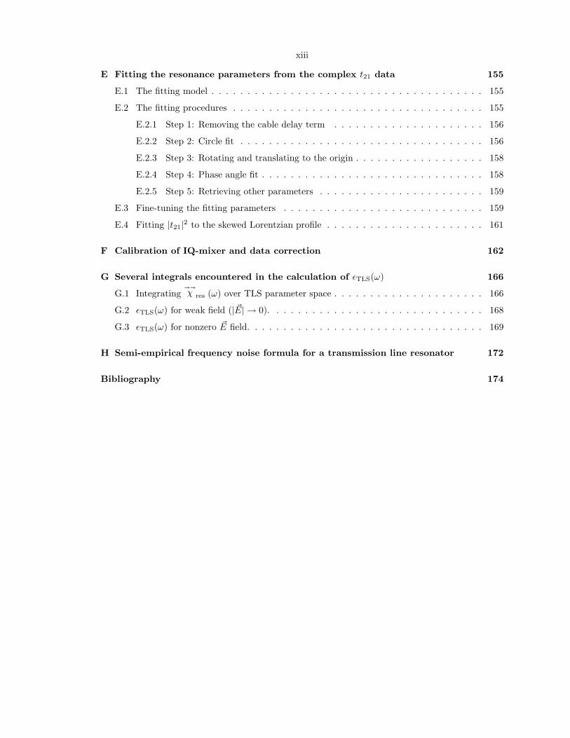
0
(d)
fr f
-
0
P
f0
f
T1
T
f-10
0
Pow
er
[dB
]
fr
fr
T2
f
(c)
T1
(b)
(a)
CPW
resonator
feedline
coupler
CPW
resonator
feedline
coupler
(f)
(g)
S21
Lki
Lm
h
1 2
Figure 1.1: Detection principle of MKIDs. a) A photon with energy hν > 2∆ breaks Cooper pairsand creates quasiparticles in a superconducting strip cooled to T < Tc. b) The superconducting stripis used as an inductive element with a variable kinetic inductance Lki and a fixed inductance Lm in amicrowave resonant circuit. The increase in the quasiparticle density changes the surface impedanceZs (mainly surface inductance Ls) which leads to a change in Lki. c) The transmission throughthe resonant circuit has a narrow dip at the resonance frequency fr which moves when Lki changes.d) The microwave probe signal acquires a phase shift when fr changes. e) Schematic illustration(not to scale) of the coplanar waveguide resonator and feedline which implement the LC resonantcircuit of (b). Blue represents the superconducting film and white represents bare substrate. f) Across-sectional view of the coplanar waveguide geometry
pairs which can move freely in the superconductor without being scattered.
However, because Cooper pairs have inertia, superconductors have a nonzero ac impedance. The
effect of the inertia of the electrons to the conductivity is included in Drude’s model and the ac
conductivity σ(ω) is given by:
σ(ω) =σdc
1 + jωτ(1.1)
where ω is the frequency, τ is the scattering time, and the jωτ term arises from the phase lag
between the current and the electric field due to the inertia of the electrons. In a normal metal
at room temperature, the electron scattering time τ is very short, on the order of 10−14 s. So up
to the microwave frequencies, ωτ ≪ 1 and the conductivity appears almost purely resistive. In
a superconductor at T ≪ Tc, both σdc → ∞ and ωτ → ∞, but the ratio σdc/ωτ remains finite.
As a result, the ac conductivity σ(ω) of a superconductor is almost purely inductive, which gives
rise to a surface impedance Zs = | ~E|/|∫~Jdz| = Rs + jωLs (see Chapter 2) that is also almost
purely inductive, ωLs ≫ Rs. When a superconductor is used as a component in an ac circuit, the

4
surface inductance Ls will contribute an inductance Lki called kinetic inductance, in addition to the
conventional magnetic inductance Lm. From an energy point of view, the inductance Lki accounts
for the energy stored in the supercurrent as the kinetic energy of the Coopers.
Cooper pairs are bound together by the electron-phonon interaction, with a binding energy
2∆ ≈ 3.52kTc[19]. At finite temperature T > 0, a small fraction of electrons are thermally excited
from the Cooper pair state. These excitations are called “quasiparticles” which are responsible for
small ac losses and a nonzero surface resistance Rs of the superconductor.
Photons with sufficient energy (hν > 2∆) may also break apart one or more Cooper pairs
(Fig. 1.1a). These “excess” quasiparticles will subsequently recombine into Cooper pairs on time
scales τqp ≈ 10−3 − 10−6 s. During this time period, the quasiparticle density will be increased by a
small amount δnqp above its thermal equilibrium value, resulting in a change in the surface impedance
δZs. Although δZs is quite small, it may be sensitively measured by using a resonant circuit
(Fig. 1.1b). Changes in Ls and Rs affect the frequency and width of the resonance, respectively,
changing the amplitude and phase of a microwave signal transmitted through the circuit (Fig. 1.1c
and Fig. 1.1d).
Although the schematic depicted in Fig. 1.1b directly suggests a lumped-element implementa-
tion, a distributed resonant circuit with a quarter wavelength coplanar waveguide (CPW) resonator
capacitively coupled to a CPW feedline (Fig. 1.1f) is mostly used in MKIDs, due to the technical
advantages that will be discussed shortly.
1.1.3 Technical advantages
MKIDs have several technical advantages:
• The fundamental noise in MKIDs is limited by the fluctuations in the quasiparticle density
caused by the random breaking of Cooper pairs into quasiparticles and recombination of quasi-
particles into Cooper pairs by thermal phonons. Because of the Poisson nature of these two
processes, this generation-recombination noise (g-r noise) is proportional to the quasiparticle
density itself, which decreases as exp(−∆/kT ) when T goes to zero. Therefore, by operating
at T ≪ Tc, in theory MKIDs can achieve a very high detector sensitivity.
• The CPW resonators are a simple planar structure that can be easily fabricated by standard
lithography from a single layer of superconducting film. Because it has no junctions, bilayers
or other difficult structures to make, even the fabrication of a large detector array is straight-
forward. Therefore, MKIDs have the advantages of low cost, high yield, and good uniformity
for the fabrication of a large detector array.
• The most attractive aspect of MKIDs is its capability for large scale frequency domain mul-
tiplexing. In MKIDs, an array of resonators, each with a different resonance frequency, are

5
coupled to a common feedline. The detectors are read out by sending a probe microwave signal
containing a comb of frequencies tuned to the unique resonance frequency of each resonator,
amplifying the transmitted signal with a cryogenic high electron mobility transistor (HEMT)
amplifier, and demultiplexing the signal at room temperature. Only one input and output
transmission line (coaxial cable) and a single HEMT is needed for the readout of the entire
array, which largely simplifies the design of readout circuits and reduces the power dissipation
at the cold stage. In contrast, the direct multiplexing of TES or STJ detectors requires several
biasing wires per detector be made and one amplifier per detector be deployed.
Recent advances in the software defined radio (SDR) technology have provided a more elegant
solution for the readout of large MKID arrays[20]. On the transmitter side, the microwave
probe signal consisting of multiple tones can be generated by upconverting (mixing an IF
signal with an local microwave oscillation signal) an IF signal, which is produced by playing a
preprogrammed waveform stored in the computer memory through a fast D/A card. On the
receiver side, the transmitted microwave signal is first downconverted and then digitized by
a fast A/D card. The demodulation can be done digitally using signal processing algorithms
operating a field programmable gate array (FPGA).
1.1.4 Applications and ongoing projects
1.1.4.1 Antenna-coupled MKIDs for millimeter and submillimeter imaging
One of the ongoing projects in our group is the development of MKIDCam[21, 22], a MKID camera
with 600 pixels, each sensing 4 colors at mm/submm wavelength (see Table 6.1), which is to be
installed at CSO in 2010.
Fig. 1.2 illustrates the design concept of a single pixel in the array. Each pixel consists of a single
slot antenna, a band-pass filter and a quarter-wave CPW resonator coupled to the feedline. The
mm/submm radiation is first collected by the slot antenna. One can think of a lot of voltage sources
being placed at the points where the microstrip lines run over across the slots. These small voltage
signals are combined by the binary microstrip summing network to deliver a stronger signal to the
filter. The path lengths between the root of the summing tree and the microstrip crossing point of
each slot are designed to be the same, which ensures that only plane waves normally incident onto
the antenna will be coherently added up, thus defineing the directionality of the antenna. The band-
pass filters used here are superconducting filters which are a compact on-chip implementation of the
lumped-element LC filter networks. Both the antenna and the filters are made of superconductor
Nb, which has a Tc = 9.2 K and gives very small loss for the mm/submm wave. The desired in-band
mm/submm signal is selected by the filter and delivered to the CPW resonator by a Nb microstrip
overlapping with the center strip of the CPW resonator near its shorted end. Because the center

6
Figure 1.2: An illustration of the pixel design in an antenna-coupled submm MKIDs array. The slotantenna, on-chip filter, CPW resonator, and feedline are shown in this illustration. This pixel usesa single slot antenna and has one filter, which is able to sense one polarization at one wavelength(color). The actual pixel used in the MKIDCam has four filters, each followed by one CPW resonator.
strip is made of superconductor Al (Tc = 1.2 K), the submm/mm wave from the Nb microstrip will
break Cooper pairs in the Al strip in the overlapping region, change the local surface impedance Zs,
and be sensed by the resonator readout circuit.
The pixel design shown in Fig. 1.2 is slightly different from the actual pixel design used in the
MKIDCam array. The pixel shown here uses one filter and can therefore sense only one color, while
the pixel in MKIDCam uses 4 filters to sense the 4 colors, with each filter followed by a CPW
resonator. In Fig. 1.2, the entire CPW resonator as well as the feedline are made of Al, while in
a MKIDCam pixel only the center strip near the shorted end, where the microstrip overlaps with
CPW, is made of Al, and the remaining part is made of Nb. This “hybrid” resonator design helps to
confine Al quasiparticles in a small sensitive region and increase the quality factor of the resonator.
More discussions on the hybrid mm/submm MKIDs will be given in Chapter 4 and Chapter 6.
1.1.4.2 MKID strip detectors for optical/X-ray
Also under development in our group is the MKID detector array for optical and X-ray detection[23].
The optical and X-ray MKIDs share a common position-sensitive strip detector design as shown in
Fig. 1.3, which is borrowed from a scheme originally used by the STJ detectors. In this scheme,
an absorber strip made of a higher-gap superconductor with a large atomic number, usually Ta
(Tc = 4.4 K and Z = 181), is used to absorb the optical/X-ray photons. These high energy photons
break Cooper pairs and generate quasiparticles in the Ta absorber. The Ta quasiparticles (with

7
Figure 1.3: An illustration of the strip detector design used in Optical/X-ray MKIDs. The optical/X-ray photon breaks Cooper pairs and generates quasiparticles in the Ta absorber. The Ta quasipar-ticles (with energy ∼ ∆Ta) diffuse to the edges of the absorber and are down-converted to Alquasiparticles (with energy ∼ ∆Al) in the Al sensor strips attached to the Ta absorber. Because∆Al < ∆Ta, the Al quasiparticles are trapped in the sensor strip and cause a change in the Alquasiparticle density, which is sensed by the resonator circuit.
energy ∼ 2∆Ta) diffuse to the edges of the absorber and are downconverted (by breaking Cooper
pairs with lower gap energy) to Al quasiparticles (with energy ∼ 2∆Al) in the Al sensor strips that
are attached to the absorber on both edges. Because ∆Al < ∆Ta, a natural quasiparticle trap forms
which prevent the Al quasiparticles from leaving the Al sensor strip. These excess quasiparticles
change the Al quasiparticle density, which is sensed by the resonator circuit. Each single photon
absorbed will give rise to two correlated pulses in the readout signals from the two resonators. The
energy deposited by the photon can be resolved by looking at the sum of the two pulse heights, while
the position where the photon is absorbed can be resolved by examining the ratio between the two
pulse heights, or the arrival time difference between the two pulses. Therefore, this scheme makes
a position-sensitive spectrometer. An energy resolution of δE = 62 eV at 5.899 keV from a X-ray
MKID strip detector has been demonstrated[24].
1.1.4.3 MKID phonon sensor for dark matter search
Dark matter, the unknown form of matter that accounts for 25 percent of the entire mass of the
universe, has long been a fascinating problem to the theoretical physicists and astrophysicists, while
the search for dark matter has been one of the most challenging experiments to the experimentalists.
Weakly interacting massive particles (WIMPs) are leading candidates for the building blocks of
dark matter. These particles have mass and interact with gravity, but do not have electromagnetic
interaction with normal matter.
It is predicted that WIMP dark matter may be directly detected through its elastic-scattering
interaction with nuclei. One of the popular detection schemes, which sets the lowest constraint for

8
(a) (b)
Figure 1.4: A proposed detector scheme of kinetic inductance phonon sensor for dark matter detec-tion using CPW ground plane trapping. (a) Cross-sectional view and (b) top view of the detector[25].
the WIMP-nucleon cross section today, is to jointly measure the effects of ionization and lattice
vibrations (or phonons) caused by the nuclear recoil from a WIMP impact event, using a crystalline
Ge or Si absorber (also called a target). By examining the ionization signal and the phonon signal,
WIMP events can be discriminated from non-WIMP events.
Currently the Cryogenic Dark Matter Search (CDMS) experiment uses 19 Ge targets (a total
mass of 4.75 kg) and 11 Si targets (a total mass of 1.1 kg), with TES phonon sensors covering the
surface of each target. As the total target mass will be significantly increased (> 100 kg) in the
next generation of CDMS experiments, how to instrument such a large target at low cost while
maintaining a high sensitivity becomes a big challenge.
MKID phonon sensors offer an interesting solution to this scaling problem. Fig. 1.4 shows a
detector scheme proposed by Golwala[25]. In this scheme, the surface of the target is covered by
frequency domain multiplexed CPW resonators. Phonons generated by the nuclear recoil arrive at
the surface and break Cooper pairs mostly in the Al ground planes. The Al quasiparticles then
diffuse to the edges of the CPW ground plane, where a narrow strip of lower gap superconductor
(Ti or W) overlaps with the Al ground planes. The Al quasiparticles will be downconverted Ti or
W quasiparticles which are trapped in the edge region and sensed by the resonator.
In another scheme proposed by the CDMS group in UC Berkeley[26], Nb strip resonators are
placed in a separate wafer as shown in Fig. 1.5. The Ge target is first coated with a thin Al film on
the surface serving as a ground plane. The strip resonators are then suspended over the ground plane
at the desired separation using spacers. The structure becomes a air-gapped microstrip (inverted
microstrip). The quasiparticles are generated in the Al ground plane and are sensed when they

9
(a) (b)
Figure 1.5: The detector scheme of the kinetic inductance phonon sensor using air-gapped microstripresonators for dark matter detection. (a) Separation of function: resonators are patterned onto astandard sized wafer, which is then affixed to the thick absorber. The absorber receives minimalprocessing. (b) Cross-sectional view of kinetic inductance phonon sensor test device. The probewafer, containing the resonators, is suspended above the absorber using metal foil spacers. Figurefrom [26]
diffuse to the region underneath the top Nb strip. One of the advantages of this scheme is that no
lithography is required on the large target, because of the separation of resonator wafer from the
target. Fairly high-Q resonators (Qr ∼ 40, 000) using this structure have been demonstrated[26].
1.2 Other applications of superconducting microwave res-
onators
Ever since the original work on MKIDs was started, superconducting microwave resonators have
attracted great attention both inside and outside the low temperature detector community. The
following shows a number of successful applications of superconducting microwave resonators, which
have been inspired by MKIDs.
1.2.1 Microwave frequency domain multiplexing of SQUIDs
The traditional time domain multiplexing of SQUID uses switching circuit to periodically select a
sensor in an array for readout. This scheme is still rather complicated in terms of fabrication and
operation. Recently, researchers in NIST[27, 28] and JPL[29, 30] are investigating the frequency
domain multiplexing of SQUIDs using superconducting resonators.
The circuit schematic of the SQUID multiplexer developed in NIST is illustrated in Fig. 1.6. The
quarterwave resonator is terminated with a single junction SQUID loop, instead of being directly

10
Figure 1.6: Schematic of the SQUID multiplexer using the quarterwave CPW resonators (modeledas parallel LC resonators). Figure from [28]
50 µm
5 µm
1 mmA
B C
Figure 1.7: Integrated circuit for cavity QED. Panel A, B, and C show the entire device consisting ofthe CPW resonator and the feedline, the coupling capacitor, and the Cooper pair box, respectively.Figure from [31]
short circuited as in MKIDs. Because of the flux-dependent Josephson inductance, the SQUID loop
acts as a flux-variable inductor. Therefore a change of the flux in the SQUID loop will modify the
total inductance, leading to a resonance frequency shift that can be read out. A prototype of this
multiplexer with high-Q (∼ 18,000) resonators has been demonstrated by the NIST group.
1.2.2 Coupling superconducting qubits to microwave resonators
The cavity quantum electrodynamic (CQED) experiments, which study the interaction between
photons and atoms (light and matter), are usually performed with laser and two-level atoms in an
optical cavity. For the first time, Wallraff et al.[31] have demonstrated that these experiments can
also be carried out with microwave photons and superconducting qubits (Cooper pair box) in a
superconducting microwave resonator. They call it “circuit QED”.
A picture of such a device is shown in Fig. 1.7. In this device, a full-wave Nb CPW resonator is
capacitively coupled to the input and output transmission lines. A Cooper pair box is fabricated in
the gap between the center strip and the ground planes and in the middle of the full-wave resonator,

11
nators
are capacitively
a
b
6 mm
10 mm
x
FIG. 2: (a) Drawing of our device showing frequency multiplexed
Figure 1.8: (a) Device drawing showing frequency multiplexed quarterwave CPW resonators. (b)A zoom-in view of a suspended nanomechanical beam clamped on both ends (with Si substrateunderneath etched off) and electrically connected to the center strip of the CPW. Figure from [36]
where the electric field is maximal, allowing a strong coupling between the qubit and the cavity. The
two Josephson tunnel junctions are formed at the overlap between the long thin island parallel to
the center conductor and the fingers extending from the much larger reservoir coupled to the ground
plane.
The coupled circuit of qubit and resonator can be described by the well-known Jaynes-Cummings
Hamiltonian[32]. It can be shown that for weak coupling g or large detuning ∆ = ε/h − fr (ε is
the two-level energy of the qubit and fr is the resonance frequency), g ≪ ∆, the reactive loading
effect of the qubit will cause the resonator frequency to shift by ±g2/∆ depending on the quantum
state of the qubit. This shift can be measured by a weak microwave probe signal. Therefore, this
dispersive measurement scheme performs a quantum non-demolition read-out of the qubit state.
Circuit-QED opens up a new path to perform quantum optics and quantum computing exper-
iments in a solid state system. Currently, circuit-QED has become a very hot area of quantum
computing research[33, 34, 35].
1.2.3 Coupling nanomechanical resonators to microwave resonators
A superconducting microwave resonator is also used in an recent experiment to read out the motion
of a nanomechanical beam, or the quantum mechanical state of a mechanical harmonic oscillator[36].
The device used for this experiment is shown in Fig. 1.8. A nanomechanical beam (50 µm long with
a 100 nm by 130 nm crosssection) is formed by electron beam lithography of an Al film deposited on

12
a Si substrate. The beam is suspended by etching off the Si substrate underneath it. Because the Al
beam is electrically connected to the center strip, the local centerstrip-to-ground capacitance depends
on the position of the beam. If the beam has a displacement or deformation, it will cause a shift in
the resonance frequency, which can be read out from the transmission measurement. In addition to
the detection of the nanomechanical motion, researchers are working on cooling the nanomechanical
resonators towards their ground state, by making use of the radiation pressure effect.

13
Chapter 2
Surface impedance ofsuperconductor
2.1 Non-local electrodynamics of superconductor and the
Mattis-Bardeen theory
It is well known that an electromagnetic field penetrates into the normal metal with a finite skin
depth δ. The skin depth can be calculated using Maxwell’s equations and Ohm’s law, which expresses
a local relationship between the current density ~Jn and the electric field ~E in the normal metal:
~Jn(~r) = σ ~E(~r) =σdc
1 + jωτ~E(~r) , (2.1)
where σdc is the DC conductivity and τ is the relaxation time of the electrons, related by τ = l/v0
to the mean free path l and the Fermi velocity v0. Because τ is usually below a picosecond at room
temperature, the condition ωτ ≪ 1 holds at microwave frequency ωτ ≪ 1, and so σ ≈ σdc. The skin
depth δ is derived to be
δ ≈
√2
ωµσdc, (2.2)
where µ is the magnetic permeability of the metal; usually µ ≈ µ0.
The local relationship Eq. 2.1 and the classic skin depth (Eq. 2.2) are valid when the electric field
~E varies little within a radius l around some point ~r, which translates to l ≪ δ. Because δ decreases
at higher frequencies and l increases at lower temperatures, a non-local relationship between ~Jn
and ~E may occur at high enough frequency or low enough temperature. A non-local relationship
replacing Eq. 2.1 was proposed by Chambers[37]:
~Jn(~r) =3σdc
4πl
∫
V
~R~R · ~E(~r′)e−R/l
R4d~r′ , (2.3)

14
where ~R = ~r′ − ~r. Eq. 2.3 is non-local because ~Jn at point ~r depends on ~E not just at that point,
but is instead a weighted average of ~E in a volume around ~r. If ~E varies little in the vicinity of ~r so
that ~E can be taken out of the integral, Eq. 2.3 returns to the local relationship.
Due to the Meissner effect, an electromagnetic field also penetrates into a superconductor over
a distance called the penetration depth λ. Similar to the classical skin effect, in the calculation of λ
both local and non-local behavior may occur. Equations reflecting a local relationship between the
supercurrent Js (assuming the two fluid model with ~J = ~Js + ~Jn) and the fields were proposed by
London[38] (known as the famous London equations):
∂
∂t~Js =
~E
µ0λ2L
, (2.4)
∇× ~Js = − 1
λ2L
~H, (2.5)
where µ0 is the vacuum permeability, ~H is the magnetic field, and λL is the London penetration
depth. At zero temperature, the London penetration depth λL0 is given by
λL0 =
√m
µ0ne2, (2.6)
where m, n, and e are the mass, density, and charge of the electron, respectively. In the London
gauge ∇ · ~A = 0, the second London equation can be written as1
~Js = − 1
λ2L
~A. (2.7)
These equations apply to superconductors where the local condition is satisfied. In general, a
non-local relationship is more appropriate, because the mean free path l may become large in high
quality superconductors at low temperatures. Based on the observation of increasing penetration
depth with increasing impurity density or decreasing mean free path, Pippard proposed an empirical
non-local equation [41]:
~Js(~r) = − 3
4πξ0λ2L
∫
V
~R~R · ~A(~r′)e−R/ξ
R4d~r′ (2.8)
with1
ξ=
1
ξ0+
1
αpl(2.9)
where ξ0, ξ are the coherence lengths of the pure and impure superconductor and αp is an empirical
1Throughout this thesis, the magnetic vector potential is defined as ~H = ∇ × ~A, which is used by Mattis andBardeen[39] and Popel[40].

15
constant. The coherence length ξ0 is related to v0 and ∆0 by
ξ0 =~v0π∆0
, (2.10)
where ∆0 is the gap parameter at zero temperature introduced by the BCS theory[42]. The coherence
length ξ0 may be thought as the minimum size of a Cooper pair as dictated by the Heisenburg
uncertainty principle.
From the BCS theory, Mattis and Bardeen have derived a non-local equation between the total
current density ~J (including the supercurrent and the normal current) and the vector potential
~A[39]:
~J(~r) =3
4π2v0~λ2L0
∫
V
~R~R · ~A(~r′)I(ω,R, T )e−R/l
R4d~r′ (2.11)
with
I(ω,R, T ) = − jπ
∫ ∆
∆−~ω
[1 − 2f(E + ~ω)][g(E) cosα∆2 − j sinα∆2]ejα∆1dE
− jπ
∫ ∞
∆
[1 − 2f(E + ~ω)][g(E) cosα∆2 − j sinα∆2]ejα∆1dE
+ jπ
∫ ∞
∆
[1 − 2f(E)][g(E) cosα∆1 + j sinα∆1]e−jα∆2dE,
and
∆1 =
√E2 − ∆2 , |E| > ∆
j√
∆2 − E2 , |E| < ∆, ∆2 =
√(E + ~ω)2 − ∆2, g(E) =
E2 + ∆2 + ~ωE
∆1∆2, α = R/(~v0),
(2.12)
where ∆ = ∆(T ) is the gap parameter at temperature T and f(E) is the Fermi distribution function
given by
f(E) =1
1 + eE
kT
. (2.13)
The function I(ω,R, T ) decays on a characteristic length scale R ∼ ξ0, which arises from the
fact that the superconducting electron density cannot change considerably within a distance of the
coherence length. Eq. 2.11 is consistent (qualitatively) with Eq. 2.8, because both the Pippard kernel
eR/ξ and the full Mattis-Bardeen kernel I(ω,R, T )eR/l express a decaying profile with a characteristic
length dictated by the smaller of l and ξ0.
In the next section of this chapter, we will start from Eq. 2.11 and evaluate the surface impedance
of superconductor step by step.
16
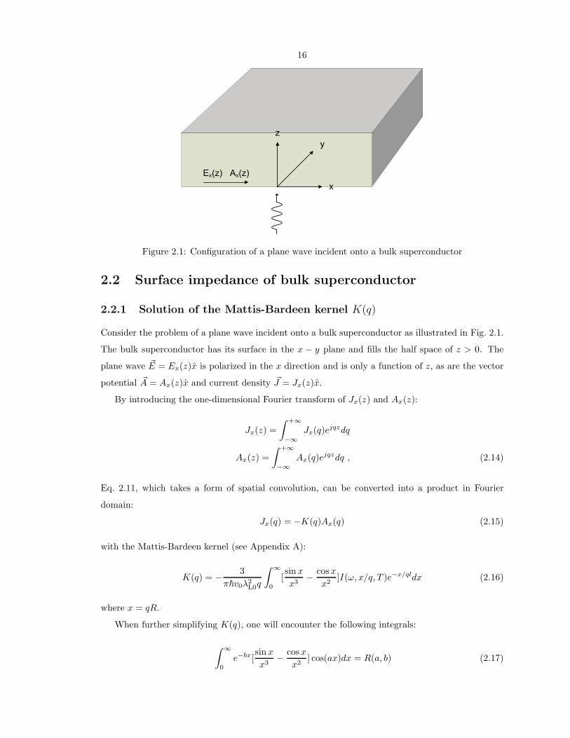
Figure 2.1: Configuration of a plane wave incident onto a bulk superconductor
2.2 Surface impedance of bulk superconductor
2.2.1 Solution of the Mattis-Bardeen kernel K(q)
Consider the problem of a plane wave incident onto a bulk superconductor as illustrated in Fig. 2.1.
The bulk superconductor has its surface in the x − y plane and fills the half space of z > 0. The
plane wave ~E = Ex(z)x is polarized in the x direction and is only a function of z, as are the vector
potential ~A = Ax(z)x and current density ~J = Jx(z)x.
By introducing the one-dimensional Fourier transform of Jx(z) and Ax(z):
Jx(z) =
∫ +∞
−∞Jx(q)ejqzdq
Ax(z) =
∫ +∞
−∞Ax(q)ejqzdq , (2.14)
Eq. 2.11, which takes a form of spatial convolution, can be converted into a product in Fourier
domain:
Jx(q) = −K(q)Ax(q) (2.15)
with the Mattis-Bardeen kernel (see Appendix A):
K(q) = − 3
π~v0λ2L0q
∫ ∞
0
[sinx
x3− cosx
x2]I(ω, x/q, T )e−x/qldx (2.16)
where x = qR.
When further simplifying K(q), one will encounter the following integrals:
∫ ∞
0
e−bx[sinx
x3− cosx
x2] cos(ax)dx = R(a, b) (2.17)

17∫ ∞
0
e−bx[sinx
x3− cosx
x2] sin(ax)dx = S(a, b). (2.18)
These integrals can be worked out by the method of Laplace transformation. The result is:
W (s = b− ja) = R(a, b) + jS(a, b) = −s2
+1
2(s2 + 1) arctan
1
s.
The derivation and the detailed expressions of R(a, b) and S(a, b) are given in Appendix A.
Finally, the kernel K(q) works out to be
ReK(q) =3
~v0λ2L0q
× ∫ ∆
max∆−~ω,−∆[1 − 2f(E + ~ω)] E2 + ∆2 + ~ωE√
∆2 − E2√
(E + ~ω)2 − ∆2R(a2, a1 + b) + S(a2, a1 + b)dE
+1
2
∫ −∆
∆−~ω
[1 − 2f(E + ~ω)][g(E) + 1]S(a−, b) − [g(E) − 1]S(a+, b)dE
−∫ ∞
∆
[1 − f(E) − f(E + ~ω)][g(E) − 1]S(a+, b)dE
+
∫ ∞
∆
[f(E) − f(E + ~ω)][g(E) + 1]S(a−, b)dE
(2.19)
ImK(q) =3
~v0λ2L0q
×−1
2
∫ −∆
∆−~ω
[1 − 2f(E + ~ω)][g(E) + 1]R(a−, b) + [g(E) − 1]R(a+, b)dE
+
∫ ∞
∆
[f(E) − f(E + ~ω)][g(E) + 1]R(a−, b) + [g(E) − 1]R(a+, b)dE
(2.20)
where b = 1/ql, a+ = a1 + a2, a− = a2 − a1, a1 = ∆1/(~v0q), and a2 = ∆2/(~v0q). When ~ω < 2∆,
the first integrals in both the real and the imaginary parts of K(q) vanish. Physically, these two
integrals represent the breaking of Cooper pairs that have a binding energy of 2∆ with photons of
energy ~ω.
2.2.2 Asymptotic behavior of K(q)
It can be shown from Eq. 2.19 that to the lowest order
W (s) =
π4 |s| → 0
13s |s| → ∞
(2.21)

18
and thus
R(a, b) =π
4, S(a, b) = 0 a2 + b2 → 0 (2.22)
R(a, b) =b
3(a2 + b2), S(a, b) =
b
3(a2 + b2)a2 + b2 → ∞. (2.23)
The asymptotic behavior of K(q) at q → 0 and q → ∞ can be derived from the asymptotic form of
W (s).
2.2.2.1 K(q → 0)
In this limit, we have
a ∼ 1
v0q∼ 1
qξ0→ ∞ (a = a1, a2, a
+, a−), b ∼ 1
ql→ ∞. (2.24)
Thus a2 + b2 → ∞ is satisfied and from Eq. 2.23
R(a, b) =b
3(a2 + b2)∝ q, S(a, b) =
b
3(a2 + b2)∝ q. (2.25)
It turns out that the terms of R and S in Eq. 2.19 and Eq. 2.20 cancel the factor 1/q in front of the
integrals. The result is that K(q) approaches a constant as q goes to zero. Because the condition
a2 + b2 ≫ 1 requires either argument be large, we arrive at the following conclusion:
K(q) = K0(ξ0, l, T ), q ≪ max 1
ξ0,
1
l (2.26)
where K0(ξ0, l, T ) is a constant dependent on the parameters such as ξ0, l, and T .
2.2.2.2 K(q → ∞)
In this limit, we have
a ∼ 1
qξ0→ 0 (a = a1, a2, a
+, a−), b ∼ 1
ql→ 0. (2.27)
Thus a2 + b2 → 0 is satisfied. Inserting Eq. 2.22 into Eq. 2.19, we find that K(q) goes as 1/q as q
becomes very large. Because the condition a2 + b2 ≪ 1 requires both arguments be small, we arrive
at the following conclusion:
K(q) =K∞(ξ0, l, T )
q, q ≫ max 1
ξ0,
1
l (2.28)
where K∞(ξ0, l, T ) is another constant.

19
I
II
III
q
K(q)
qK0
K∞
Figure 2.2: A sketch of K(q)
2.2.2.3 A sketch of K(q)
Fig. 2.2 depicts the general behavior of K(q), which divides into three regimes. In regime I, where
q ≪ max 1ξ0, 1
l , K(q) approaches the constant K0(ξ0, l, T ). In regime III, where q ≫ max 1ξ0, 1
l K(q) goes as K∞(ξ0, l, T )/q. Regime II is the transition regime.
The behavior of K(q) shown in Fig. 2.2 agrees with our earlier discussion of the spatial domain
Mattis-Bardeen kernel I(ω,R, T )e−R/l. Because the kernel I(ω,R, T )e−R/l decays on a characteristic
length of R ∼ minξ0, l, its Fourier transform K(q) will span a width of q ∼ max1/ξ0, 1/l.
2.2.3 Surface impedance Zs and effective penetration depth λeff for spec-
ular and diffusive surface scattering
The surface impedance Zs is usually defined as the ratio between the transverse components of ~E
field and ~H field on the surface of the metal. In our configuration, as shown in Fig. 2.1,
Zs =Ex
Hy|z=0. (2.29)
In the following, we will derive expressions which relate Zs to the Fourier domain Mattis-Bardeen
kernel function K(q).
From the Maxwell equation ∇× ~E = −jωµ0~H and the relationship ~H = ∇× ~A, we find for our

20
configuration
Ex(z) = −jωµ0Ax(z)
Hy(z) =dAx(z)
dz
Zs = −jωµ0Ax(z)
dAx(z)/dz
∣∣∣∣z=0
. (2.30)
Using another Maxwell Equation ∇× ~H = jωǫ0 ~E+ ~J and neglecting the displacement current term
(which is much smaller than ~J in metal), we get
Jx(z) = −d2Ax(z)
dz2. (2.31)
On the other hand, we have derived in Appendix A the one-dimensional form of the Mattis-Bardeen
equation equivalent to Eq. 2.11:
Jx(z) =
∫K(η)Ax(z′)dz′
K(η) =3
4π~v0λ2L
∫ ∞
1
du(1
u− 1
u3)I(ω, |η|u, T )e−|η|u/l (2.32)
with η = z′ − z. Here K(η) is the inverse Fourier transform of −K(q) discussed in Section 2.2.1.
There is some subtlety in combining Eq. 2.31 and Eq. 2.32 to obtain a workable equation for
Ax(z). It turns out that how the electrons scatter from the surface matters, because we are studying
the current distribution in a region very close to the surface. The usual assumption is that a portion
p of the electrons reflect from the surface specularly (after reflection, the normal component of the
momentum of the electron flips its sign) and the remaining portion 1 − p of the electrons scatter
diffusively (after scattering the momentum of the electron is randomized)[43].
For the perfect specular scattering case (p = 1), one can make a even continuation of the field
and current into the z < 0 space which leads to the following integro-differential equation:
− d2Ax(z)
dz2=
∫ ∞
−∞K(η)Ax(z′)dz′. (2.33)
For the perfect diffusive scattering case (p = 0), one can derive another integro-differential
equation:
− d2Ax(z)
dz2=
∫ ∞
0
K(η)Ax(z′)dz′. (2.34)
A complete solution of the equation is not necessary for the purpose of evaluating the surface
impedance, because only the ratio of A and its derivative on the surface is needed, according to

21
Eq. 2.30. However, even solving for this ratio from the two integro-differential equations is non-
trivial. The solution is obtained in Fourier domain, and only the ultimate results are quoted here:
Perfect specular scattering: Zs =jµ0ω
π
∫ ∞
−∞
dq
q2 +K(q)(2.35)
Perfect diffusive scattering: Zs =jµ0ωπ∫∞
0ln(1 + K(q)
q2 )dq(2.36)
where K(q) is the one-dimensional Mattis-Bardeen kernel in Fourier space. Please refer to Reuter
and Sondheimer [43] and Hook [44] for the detailed derivations of these two equations.
Although formula for the specular scattering case is mathematically simpler than the diffusive
scattering case, the latter is considered to better represent the real situation of electron scattering
at the metal surface and is more widely used. In this thesis, we adopt the diffusive scattering
assumption and use Eq. 2.36 to evaluate surface impedance.
The surface impedance Zs generally has a real and imaginary part
Zs = Rs + jXs = R+ jωLs = Rs + jωµ0λeff (2.37)
where Rs, Xs, and Ls are called surface resistance, surface reactance, and surface inductance,
respectively, and λeff is called the effective penetration depth. For temperature much lower than
Tc, usually Rs ≪ Xs. If we assume that Jx(z), Hy(z), and Ax(z) all decay into the superconductor
exponentially as e−z/λeff , and ignoring Rs, we can immediately see from Eq. 2.30 that
Zs ≈ jωµ0λeff . (2.38)
For diffusive scattering, according to Eq. 2.36, λeff can be calculated by
λeff =π
Re[∫∞
0 ln(1 + K(q)q2 )dq
] . (2.39)
2.2.4 Surface impedance in two limits
It is useful to rewrite Eq. 2.36 into the following form
Zs = jµ0ωλL0π
∫∞0 ln(1 +
λ2L0
K(Q/λL0)
Q2 )dQ(2.40)
where both λ2L0K(Q/λL0) and Q are dimensionless.
According to Eq. 2.26 and Eq. 2.28, K(Q/λL0) has the following asymptotic behavior for small
and large Q:
22
Regime I: Q≪ maxλL0
ξ0, λL0
l , K(Q/λL0) = K0(ξ0, l, T ) (2.41)
Regime III: Q≫ maxλL0
ξ0, λL0
l , K(Q/λL0) = λL0K∞(ξ0, l, T )/Q. (2.42)
2.2.4.1 Extreme anomalous limit
In the extreme anomalous approximation, one assumes that Regime III holds for all Q of importance
in the integral in Eq. 2.40, so K(Q) can be replaced by its asymptotic form of Eq. 2.42.
Zs = jµ0ωλL0π
∫∞0
ln(1 +λ3L0
K∞(ξ0,l,T )
Q3 )dQ
= jµ0ω[
√3
2K∞(ξ0, l, T )−1/3] (2.43)
λeff = Re
[√3
2K∞(ξ0, l, T )−1/3
](2.44)
where∫∞0
ln(1 + 1/x3)dx = 2π/√
3 is used.
According to Eq. 2.42, the condition for the extreme anomalous limit is
ξ0 ≫ λL0 AND l ≫ λL0. (2.45)
In fact, this condition can be relaxed to
ξ0 ≫ λeff AND l ≫ λeff . (2.46)
This is because the lower limit of the integral∫∞0 ln(1+1/x3)dx can be set to a small number ǫ instead
of 0 without significant error. For qualitative discussion, let’s take ǫ = 1, which corresponds to a
lower limit of Ql ≈ 3√λ3
L0K∞(ξ0, l, T ) ≈ λL0/λeff in the integral of Eq. 2.40. For self consistency,
K(Q) for Q > Ql must be all in Regime III and therefore Ql must satisfy the condition Ql ≈λL0/λeff ≫ maxλL0
ξ0, λL0
l , which leads to the condition Eq. 2.46.
According to the condition given by Eq. 2.45, the extreme anomalous limit occurs when the
effective penetration depth λeff , which is the characteristic length scale of the penetrating magnetic
field, is much less than the the smaller of ξ0 and l, which is the decay length of the Mattis-Bardeen
kernel. Extreme anomalous effect may also occur in a normal metal at high frequency and low
temperature, when the classical skin depth δ becomes shorter than the scattering length l.

23
2.2.4.2 Local limit
In the local approximation, one assumes that Regime I holds for all Q of importance in the integral
in Eq. 2.40; K(Q) can be replaced by its asymptotic form in Eq. 2.41.
Zs = jµ0ωλL0π
∫∞0 ln(1 +
λ2L0K0(ξ0,l,T )
Q2 )dQ
= jµ0ω[K0(ξ0, l, T )−1/2]
λeff = Re[K0(ξ0, l, T )−1/2
](2.47)
where∫∞0
ln(1 + 1/x2)dx = π is used.
The condition for this approximation to be valid, according to Eq. 2.41, is
ξ0 ≪ λL0 OR l ≪ λL0. (2.48)
Similar to the extreme anomalous case, this condition can be relaxed to
ξ0 ≪ λeff OR l ≪ λeff . (2.49)
Another widely used definition of local (or dirty) limit in the literature is
l ≪ ξ0 AND l ≪ λeff (2.50)
which is stronger than condition of Eq. 2.49. So the local approximation and result of effective
penetration Eq. 2.47 is guaranteed to be valid in such defined local limit.
According to the condition given by Eq. 2.48, the local limit occurs when the characteristic length
scale of the Mattis-Bardeen kernel (the smaller of ξ0 and l) is much smaller than the length scale of
the penetrating magnetic field (λeff). Therefore, the vector potential Ax(z′) ≈ Ax(z) can be taken
out of the integral in Eq. 2.32 as a constant, leading to a local equation. The local equation can be
expressed in terms of K0(ξ0, l, T ). With K(q) ≈ K0(ξ0, l, T ) for all q, K(η) = K0(ξ0, l, T )δ(η). The
one-dimensional Eq. 2.32 reduces to
Jx(z) = −K0(ξ0, l, T )Ax(z) =K0(ξ0, l, T )
jµ0ωEx(z). (2.51)
If a complex conductivity
σ =K0(ξ0, l, T )
jµ0ω(2.52)
is defined, the problem can be solved by using Ohm’s law J = σE, as if it were a normal metal with
conductivity σ. This complex conductivity will be discussed in more detail later in this chapter.

24
2.2.5 Numerical approach
Analytical formulas for Zs may be derived for a few special cases under certain approximations,
which will be discussed later in this chapter. In general, Zs has to be evaluated by numerical
approach. The task for such a numerical program is to calculate a two-fold integral: for a given q
the evaluation of K(q) involves 6 energy integrals for hω > 2∆ or 4 integrals for hω < 2∆, according
to Eq. 2.19 and Eq. 2.20; then an integral of K(q) over q gives Zs, as defined in Eq. 2.36. To carry
out these numerical integrals efficiently and robustly, a few tactics have been used, which are briefly
discussed in Appendix B.
2.2.6 Numerical results
A numerical program “surimp” was developed in the C++ language to implement the theory and
algorithm discussed above. To calculate the surface impedance, the program takes frequency ω and
temperature T as two independent variables, and requires five material-dependent parameters to be
specified: the transition temperature Tc, the energy gap at zero temperature ∆0 (or the ratio of
∆0 to kT ), the London penetration depth at zero temperature λL0, the mean free path l and the
coherence length ξ0 (or the Fermi velocity v0).
In addition, the temperature dependent gap function ∆(T ) is calculated using a subroutine
borrowed from the “Supermix” software, a package developed at Caltech originally for the super-
conducting SIS mixer design[45]. In “Supermix”, the reduced energy gap ∆(T )/∆0 as a function of
T/Tc is interpolated from a table of experimentally measured values given by Muhlschlegel[46] for
T/Tc > 0.18, and from the low temperature approximate expression (see Eq. 2.88)
∆(T )
∆0≈ exp[−
√2πkT
∆0exp(−∆0
kT)] ≈ exp[−
√3.562x exp(−1.764/x)] (2.53)
for x = T/Tc < 0.18, where the BCS value ∆0 = 1.762kTc is assumed in the right-hand side of
Eq. 2.53.
2.2.6.1 λeff of Al and Nb at zero temperature
As a first application of the program “surimp”, we calculate the surface impedance Zs of Al and Nb
at T = 0 K and f = 6 GHz. The material parameters are taken from Popel [40] and are listed in
Table 2.1, except that the BCS ratio of ∆0/kT = 1.76 is used. The program gives λeff = 51.4 nm
for Al and λeff = 63.5 nm for Nb. From the listed material dependent parameters, we see that Al is
in the extreme anomalous limit case while Nb is in the local limit case.

25
Table 2.1: λeff of bulk Al and Nb.Al Nb
Tc [K] 1.2 9.2λL0 [nm] 15.4 33.3
v0 [106 m/s] 1.34 0.28ξ0[nm] 1729 39l [nm] 10000 20
∆0 [meV] 0.182 1.395∆0
kTc1.76 1.76
λeff (0 K, 6 GHz) [nm] 51.4 63.5
0 0.1 0.2 0.3 0.4 0.5 0.6 0.7 0.8 0.9 1 1.1 1.20
1
2
3
4
5x 10
−3
T (K)
Z (
Ω)
RX
Figure 2.3: Surface resistance Rs and surface reactanceXs of aluminum as a function of temperatureT . The material parameters used in the calculation are from Table 2.1
2.2.6.2 Temperature dependence of Zs
In this example, we use the program “surimp” to calculate the temperature dependence of surface
impedance. The surface resistance Rs and surface inductance Xs (or the real and imaginary part
of Zs) of Al are calculated for T from 0 to 1.15 K (slightly below Tc = 1.2K) and the results are
plotted in Fig. 2.3. As expected from the theory, we see that Rs goes to zero as T → 0 while Xs
approaches a nonzero finite value Xs(0).
The temperature dependence of Zs predicted by “surimp” can be tested by fitting it to the data
of variation of resonance frequency fr and quality factor Qr of a superconducting resonators as a
function of bath temperature. The relationships between fr, Qr and Xs, Rs are
δfr
fr=
fr(T ) − fr(0)
fr(0)= −α
2
Xs(T ) −Xs(0)
Xs(0)= −α
2
δλeff
λeff
δ1
Qr=
1
Qr(T )− 1
Qr(0)= α
Rs(T ) −Rs(0)
Xs(0)(2.54)

26
0.15 0.2 0.25 0.3−5
−4
−3
−2
−1
0
1x 10
−5
T (K)
δ f r/f r
datafit
(a) δfrfr
vs. T
0.15 0.2 0.25 0.3−0.5
0
0.5
1
1.5
2
2.5
3
3.5x 10
−5
T (K)
δ 1/
Q
datafit
(b) δ 1
Qrvs. T
0 0.5 1 1.5
x 10−3
−6
−5
−4
−3
−2
−1
0
1x 10
−5
δ Xs/X
s
δ f 0/f 0
datafit
(c) δfrfr
vs. δXsXs
0 1 2 3 4 5
x 10−4
−1
0
1
2
3
4x 10
−5
Rs/X
s
δ (1
/Q)
datafit
(d) δ 1
Qrvs. δRs
Xs
Figure 2.4: Fractional resonance frequency shift δfr
frand change in inverse quality factor δ 1
Qrvs.
temperature T . Data measured from a Al resonator with film thickness d = 220 nm, center stripwidth s = 3 µm, gap width g = 2 µm, fr = 6.911 GHz, Qr = 68000, and Tc = 1.25 K. ∆0 =0.181 meV and α = 0.07 is obtained from the best fit. Other material-related parameters are fromTable 2.1.

27
where α is the kinetic inductance fraction. Eq. 2.54 will be derived in the next two chapters. The
measured δfr/fr and δ1/Qr can be fitted to the calculated δXs/Xs and δRs/Xs with a simple linear
fitting model according to Eq. 2.54. The energy gap ∆0 and the kinetic inductance fraction α are
taken as two fitting parameters. Tc can be measured by experiment. Other parameters are taken
from the literature and set fixed. The data of fr(T ) and Qr(T ) from an Al resonator is fitted in this
way and the result is shown in Fig. 2.4, which shows a good agreement between data and calculation.
2.2.6.3 Frequency dependence of Zs
0 2 4 6 830
40
50
60
70
80
90
hf/kTC
λ eff (
nm)
T=0T=0.7T
c
T=0.8Tc
T=0.9Tc
Figure 2.5: Frequency dependance of the effective penetration depth λeff of an Al bulk supercon-ductor. The material parameters are from Table 2.1 except ∆0 = 1.70kTC.
The frequency dependance of effective penetration depth of Al is calculated and plotted in
Fig. 2.5. As a verification of our calculation, we use exactly the same material parameters used
by Popel in Fig. 15 of Ref. [40]. Comparing Fig. 2.5 to Fig. 15 of Ref. [40], we find that the
frequency dependence calculated by “surimp” is identical to that calculated by Popel.
2.3 Surface impedance of superconducting thin films
2.3.1 Equations for specular and diffusive surface scattering
One can also apply the Mattis-Bardeen equations to the case of thin films. Consider a plane super-
conductor with thickness d as shown in Fig. 2.6. If the film is thin enough, the magnetic field can
penetrate through the film and both ~H and ~J can be nonzero inside the film, which is different from
the bulk case.

28
x x
z=d
z=0
Figure 2.6: Configuration of a plane wave inci-dent onto a superconducting thin film
By(0)
z=d
z=0
z=2dBy(0)
z=-2d
z=-d
……
z=3d
z=4d
Figure 2.7: Field configuration used by Srid-har to calculate Zs of a thin film assumingspecular scattering boundary condition atboth interfaces
Again, to apply the Mattis-Bardeen equations one has to assume either specular scattering or
diffusive scattering at the surface. For specular scattering boundary at both sides of the film, the
problem can be solved by mirroring the field and current repeatedly to fill the entire space (see
Fig. 2.7) and applying the equation
− d2Ax(z)
dz2=
∫ ∞
−∞K(η)Ax(z′)dz′, η = z′ − z (2.55)
which can easily be solved in a similar manner as in the bulk case. The result is derived by Sridhar[47]
to be
Zs =iµ0ω
d
+∞∑
n=−∞
1
q2n +K(qn)(2.56)
where qn = nπ/d. Comparing Eq. 2.56 to Eq. 2.35, we see that the only change is that the integral
in the bulk case has been replace by an infinite series in the thin film case.
For the diffusive scattering boundary condition, the equation is
− d2Ax(z)
dz2=
∫ d
0
K(η)Ax(z′)dz′, η = z′ − z (2.57)
and unfortunately has to be solved numerically.

29
2.3.2 Numerical approach
There are two tasks in the numerical calculation of surface impedance of a thin film: evaluating the
kernel function K(η) and solving the integro-differential equation of Eq. 2.57.
2.3.2.1 Implementing the finite difference method
N
2
1
0
N-1
Figure 2.8: Thin film divided into N slices
The integro-differential equation of Eq. 2.57 can be solved numerically by the finite difference
method (FD). To implement FD method, we first divide the film into N thin slices of equal thickness
t=d/N (see Fig. 2.8). Then we follow the standard procedures to convert Eq. 2.57 into a discrete
FD equation. On the left-hand side, we employ the simple three-point approximation formula
d2Ax(z)
dz2≈ (An+1 − 2An +An−1)/t
2. (2.58)
On the right-hand side, we apply the simple extended trapezoidal rule to approximate the integral
as a sum ∫ d
0
K(η)Ax(z′)dz′ ≈ t
N∑
n′=0
Knn′A(n′) (2.59)
where
Knn′ =
12K(|n− n′| t) if n′ = 0 or N
1t
∫ (n+1/2)t
(n−1/2)t K(|nt− x′|)dx′ if n′ = n
K(|n− n′| t) otherwise
. (2.60)

30
So we get the following FD equations
An+1 − 2An +An−1 = −t3N∑
n′=0
Knn′A(n′), n = 1, ..., N − 1. (2.61)
2.3.2.2 Boundary condition
Eq. 2.61 provides N − 1 linear equations with N + 1 unknowns (A0 ... AN ), so two more equations
are needed. The two additional equations come from the boundary conditions at the interfaces at
z = 0 and z = d. In the configuration of Fig. 2.6, both sides of the film are connected to free space
and the electromagnetic wave is incident from z = 0 into the film. In this case, at z = 0 one can
assume either boundary conditions of the first kind
A(z)|z=0 = 1 ⇒ A0 = 1 (2.62)
or of the second kind
Hy(0) =dA(z)
dz
∣∣∣∣z=0
= 1 ⇒ A1 −A0 = t (2.63)
where a two point formula for dA(z)/dz is used. Physically, the former specifies a vector potential
and the latter specifies a magnetic field on the z = 0 surface.
At the interface of z = d, one usually assumes that the transmitted wave sees the free space
impedance
Z0 = −jωµ0A(z)dA(z)
dz
∣∣∣∣∣z=d
⇒ (1 +jωµ0
Z0t)AN −AN−1 = 0, (2.64)
Because the free space impedance Z0 ≈ 377 Ω is usually much larger than the surface impedance of
the film, boundary condition Eq. 2.64 is virtually equivalent to
Hy(d) =dA(z)
dz
∣∣∣∣z=d
= 0 ⇒ AN = AN−1 (2.65)
which physically forces a zero magnetic field on the z = d surface.
2.3.2.3 Retrieving the results
With proper boundary conditions, the FD problem is ready to solve. The N + 1 linear equations
can easily be solved with standard numerical algorithms. Unfortunately, we can not utilize a sparse
algorithm to accelerate the calculation.
For thin films, the transmitted wave is often important and can not be neglected. In these cases,
it is often not enough to consider only the surface impedance at the surface z = 0. We can generalize

31
the concept of surface impedance and define a pair of impedances for the thin film
Z11 =Ex(0)
Hy(0)= −jωµ0
Ax(z)|z=0
dAx(z)/dz|z=0= −jωµ0t
A0
A1 −A0(2.66)
Z21 =Ex(d)
Hy(0)= −jωµ0
Ax(z)|z=d
dAx(z)/dz|z=0= −jωµ0t
AN
A1 −A0(2.67)
Instead of returning one impedance, both Z11 and Z21 are calculated from the solution and reported
by our numerical program.
In the case that the electromagnetic wave is incident from one side of the thin film (d < λeff),
with the other side exposed to the free space, we have Hy(d) ≈ 0 (see the previous discussion of
Eq. 2.65) and Hy(0) = K =∫ d
0 Jxdz according to Ampere’s law, where K represents the sheet
current (current flowing in the entire film thickness). Therefore the electric fields at the two surfaces
are given by
Ex(0) = Z11K, Ex(d) = Z21K. (2.68)
In the anti-symmetric excitation case, as in a TEM mode of a superconducting coplanar waveg-
uide (discussed in more detail in the next chapter), the electromagnetic wave is incident from both
sides of the film with Hy(0) = −Hy(d). One can decompose this problem into two problems, each
with a wave incident from one side. It can be shown that in this anti-symmetric excitation case,
Hy(0) = −Hy(d) = K/2
Ex(0) = Ex(d) = (Z11 + Z21)K/2. (2.69)
2.3.3 Numerical results
With slight modification to “surimp”, a program “surimpfilm” is developed to calculate the surface
impedance of a superconducting thin film. The program takes ω and T as independent variables
and the same 5 material parameters. It takes the film thickness d and the number of subdivisions
to the film N as two additional parameters. Besides, all 3 types of boundary conditions (specifying
value of A, value of H or the load impedance Z) can be applied to both the top side and the bottom
side of the film. The values of generalized surface impedance Z11 and Z12 are returned from the
program.
2.3.3.1 λeff of Al thin film
We use “surimpfilm” to calculate the thickness dependence of surface impedance for Al at T = 0 K
and f = 6 GHz. The result is shown in Fig. 2.9. We see that Z11 approaches its bulk value when the
thickness is large compared to the bulk penetration depth (roughly d > 3λeff) and Z12 goes to zero,
implying no magnetic field penetrates through. As the thickness of the film is reduced, both Z11

32
101
102
103
100
101
102
103
104
d (nm)
λ eff (
nm)
~1/d2
λeff1
λeff2
Figure 2.9: Effective penetration depth of Al thin film vs. thickness. f = 6 GHz, T = 0 K, andother material related parameters are from Table 2.1, except that the mean free path l is set to thefilm thickness d. In the calculation, N = 400 division is used. The two effective penetration depthsare defined as λeff1 = Z11
jωµ0and λeff2 = Z21
jωµ0.
and Z21 increase. Ultimately when the film is very thin, Z11 and Z21 become equal, which implies
that the film is completely penetrated. We also notice that the impedance goes as 1/d2, which will
be explained later in this chapter.
2.4 Complex conductivity σ = σ1 − jσ2
The concept of complex conductivity σ = σ1 − jσ2 was first introduced by Glover and Tinkham[48]
for the superconding states. σ1 and σ2 are expressed by two integrals[39]
σ1
σn=
2
~ω
∫ ∞
∆
[f(E) − f(E + ~ω)](E2 + ∆2 + ~ωE)√E2 − ∆2
√(E + ~ω)2 − ∆2
dE
+1
~ω
∫ −∆
∆−~ω
[1 − 2f(E + ~ω)](E2 + ∆2 + ~ωE)√E2 − ∆2
√(E + ~ω)2 − ∆2
dE (2.70)
σ2
σn=
1
~ω
∫ ∆
max∆−~ω,−∆
[1 − 2f(E + ~ω)](E2 + ∆2 + ~ωE)√∆2 − E2
√(E + ~ω)2 − ∆2
dE. (2.71)
We recall that the expression for K(q) in Eq. 2.19 and Eq. 2.20 generally has 4 integrals in the
real part and 2 integrals in the imaginary part. We will show that under certain conditions some of
the integrals vanish and the total 6 integrals reduce to the 3 integrals of σ1 and σ2. In these cases,
Zs and λeff have simplified expressions in terms of σ1 and σ2.

33
2.4.1 Surface impedance Zs in various limits expressed by σ1 and σ2
2.4.1.1 Thick film, extreme anomalous limit
In the extreme anomalous limit, both Zs and λeff are related only to the value of K∞(ξ0, l, T )
according to Eq. 2.44. It can be shown by comparing the asymptotic expression of K(q) at q → ∞to the expression of σ in Eq. 2.70 and 2.71 that
K∞(ξ0, l, T ) =3πω
4v0λ2L0
σ2 + jσ1
σn. (2.72)
Thus
Zs =j√
3µ0ω
2[
3πω
4v0λ2L0
σ2 + jσ1
σn]−1/3. (2.73)
2.4.1.2 Thick film, local limit
In the local limit, both Zs and λeff are related only to the value of K0(ξ0, l, T ) according to Eq. 2.47.
It can be shown by comparing the asymptotic expression of K(q) at q → 0 to the expression of σ in
Eq. 2.70 and 2.71 that
K0(ξ0, l, T ) =ωl
v0λ2L0
σ2 + jσ1
σn. (2.74)
From Eq. 2.6 and the expression of σn
σn =ne2τ
m(2.75)
where n, e, and m are the density, charge, and mass of the electron, respectively, it can be derived
that
λL0 =
√l
µ0σnv0. (2.76)
Inserting Eq. 2.76 into Eq. 2.74, we get another equivalent expression of K0(ξ0, l, T )
K0(ξ0, l, T ) = jωµ0(σ1 − jσ2) (2.77)
which is consistent with Eq. 2.52. It follows from Eq. 2.47 that
Zs = jµ0ω[ωl
v0λ2L0
σ2 + jσ1
σn]−1/2
or
Zs =
√jµ0ω
σ1 − jσ2. (2.78)

34
We again see that Zs of a superconductor in the local limit can be directly obtained by substi-
tuting σ = σ1 − jσ2 for σn in the corresponding classical formulas.
2.4.1.3 Thin film
If the film thickness t is smaller than the electron mean free path in the bulk case l∞, l will be
limited by surface scattering and l ≈ d. If in addition the local condition l ≪ ξ0 and l ≪ λL0 are
satisfied, the local equation ~J = σ ~E applies. Moreover, if the film thickness satisfies d ≪ λeff , the
field penetrates through the entire film and the current distribution is almost uniform across the
film with Jx(z) ≈ Jx(0), as is the electric field Ex(z) ≈ Ex(0). The following expression of Zs can
be derived
Zs = Z11 = Z21 =Ex(0)
∫ d
0 Jx(z)dz=
1
(σ1 − iσ2)d, (2.79)
where Z11 and Z12 are defined in Eq. 2.66 and 2.67. Because σ goes as 1/l ∼ 1/d, Zs has a 1/d2
dependence on the film thickness d.
2.4.2 Change in the complex conductivity δσ due to temperature change
and pair breaking
2.4.2.1 Relating δZs to δσ
MKIDs operate on a principle that the surface impedance Zs of a superconducting film changes
when photons break Cooper pairs and generate quasiparticles (QPs)[14, 16]. The responsivity of
MKIDs is related to dZs/dnqp, where nqp is the QP density.
It follows from the discussion in the previous section that the change in Zs is related to the
change in σ by
δZs
Zs= γ
δσ
σ, γ =
−1/2 Thick film, local limit
−1/3 Thick film, extreme anomalous limit
−1 Thin film, local limit
. (2.80)
Thus, dσ/dnqp becomes an important quantity in discussing responsivity of MKIDs.
2.4.2.2 Effective chemical potential µ∗
One straightforward way of calculating dσ/dnqp is through dσ/dnqp = ∂σ(T )/∂T∂nqp(T )/∂T (the ratio between
the change in the conductivity and the change in the quasiparticle density, both caused by a change

35
in the bath temperature) from Eq. 2.70, Eq. 2.71, and
nqp = 4N0
∫ ∞
0
1
1 + eE
kT
dǫ, ǫ =√E2 − ∆2 (2.81)
where N0 is the single spin density of states. The result from such a calculation gives δσ due to a
change in thermal QP density from a change in bath temperature, which does not directly apply
to excess QPs from pair breaking. To account for excess QPs, we adopt Owen and Scalapino’s
treatment[49] and introduce an effective chemical potential µ∗ to the Fermi distribution function
f(E;µ∗, T ) =1
1 + eE−µ∗
kT
. (2.82)
Physically, Eq. 2.82 treats the QPs as a Fermi gas with a thermal equilibrium distribution char-
acterized by the chemical potential µ∗ and the temperature T . This assumption is valid because at
low temperatures, phonons with energy less than 2∆ (under-gap phonons) are much more abundant
than the phonons with energy larger than 2∆ (over-gap phonons); therefore the time scale τl for
excess QPs to thermalize with the lattice (phonon) temperature T (assisted by under-gap phonons)
is much shorter than the time scale τqp for excess QPs to recombine (assisted by over-gap phonons);
as a result, during the time τl < t < τqp, the QPs may be described using the Fermi function given
by Eq. 2.82.
With the introduction of µ∗, the total QP density nqp (including both thermal and excess
QPs), the superconducting gap ∆, and the complex conductivity σ can be rederived by substi-
tuting f(E;µ∗, T ) for f(E;T ) in the corresponding BCS formula and the Mattis-Bardeen formula.
The relevant equations now modify to
nqp = 4N0
∫ ∞
0
1
1 + eE−µ∗
kT
dǫ, ǫ =√E2 − ∆2 (2.83)
1
N0V=
∫~ωc
0
tanh E−µ∗
2kT
Edǫ (2.84)
σ1
σn=
2
~ω
∫ ∞
∆
[f(E;µ∗, T ) − f(E + ~ω;µ∗, T )](E2 + ∆2 + ~ωE)√E2 − ∆2
√(E + ~ω)2 − ∆2
dE
+1
~ω
∫ −∆
∆−~ω
[1 − 2f(E + ~ω;µ∗, T )](E2 + ∆2 + ~ωE)√E2 − ∆2
√(E + ~ω)2 − ∆2
dE (2.85)
σ2
σn=
1
~ω
∫ ∆
∆−~ω
[1 − 2f(E + ~ω;µ∗, T )](E2 + ∆2 + ~ωE)√∆2 − E2
√(E + ~ω)2 − ∆2
dE. (2.86)

36
2.4.2.3 Approximate formulas of ∆, nqp, σ, and dσ/dnqp for both cases
Under the condition that ~ω ≪ ∆ (Cond. 1), kT ≪ ∆ (Cond. 2) and e−E−µ∗
kT ≪ 1 (Cond. 3),
Eq. 2.83–2.86 have the following analytical approximate formula[50]:
nqp = 2N0
√2πkT∆e−
∆−µ∗
kT (2.87)
∆
∆0= 1 −
√2πkT
∆e−
∆−µ∗
kT = 1 − nqp
2N0∆(2.88)
σ1
σn=
4∆
~ωe−
∆−µ∗
kT sinh(ξ)K0(ξ), ξ =~ω
2kT(2.89)
σ2
σn=
π∆
~ω[1 − 2e−
∆−µ∗
kT e−ξI0(ξ)] (2.90)
where In, Kn are the nth order modified Bessel function of the first and second kind, respectively
The first two conditions (Cond. 1 and Cond. 2) are apparently satisfied by a typical Al MKID
with Tc = 1.2 K and microwave frequency ω/2π below 10 GHz. Meanwhile, the QP density due to
pair breaking from a photon with energy hν is estimated by nqp ≈ hν∆V . Assuming a sensing volume
V ∼ 3 µm× 0.2 µm× 100 µm (center strip width × film thickness × quasiparticle diffusion length)
and taking T=0.1 K, N0 = 1.72 × 1010 µm−3eV−1, and ∆ = 0.18 meV for Al, e−E−µ∗
kT is estimated
from Eq. 2.87 to be 0.1 for a 6 keV photon and 1.4 × 10⁻⁵ for a 1 eV photon, both much less than
1. Thus for Al MKIDs up to X-ray band, the third condition (Cond. 3) is also satisfied.
Now we are ready to derive σ and its derivative for the two cases.
Case 1: thermal QPs due to temperature change
In Eq. 2.87–2.90, only two of the four variables ∆, nqp, µ∗, and T are independent. By taking
µ∗ and T as independent variables, setting µ∗ = 0, and keeping only the lowest-order terms in
Eq. 2.87–2.90, we arrive at the following results
σ1(T )
σn=
4∆0
~ωe−
∆0kT sinh(ξ)K0(ξ) (2.91)
σ2(T )
σn=
π∆0
~ω[1 −
√2πkT
∆0e−
∆0kT − 2e−
∆0kT e−ξI0(ξ)] (2.92)
nqp(T ) = 2N0
√2πkT∆0e
−∆0kT (2.93)
dσ1
dnqp= σn
1
N0~ω
√2∆0
πkTsinh(ξ)K0(ξ)
∆0
kT − ξ cosh(ξ)sinh(ξ) + ξK1(ξ)
K0(ξ)
∆0
kT + 12
(2.94)
dσ2
dnqp= σn
−π2N0~ω
[1 +
√2∆0
πkTe−ξI0(ξ)
∆0
kT + ξ − ξ I1(ξ)I0(ξ)
∆0
kT + 12
] (2.95)
where the directives are evaluated by dσ/dnqp = ∂σ(T )/∂T∂nqp(T )/∂T .
Case 2: excess QPs due to pair breaking

37
Using Eq. 2.87 to suppress the explicit dependence of µ∗, taking nqp and T as independent
variables and keeping the lowest-order terms in Eq. 2.88–2.90, we arrive at the following result
σ1(nqp, T )
σn=
2∆0
~ω
nqp
N0
√2πkT∆0
sinh(ξ)K0(ξ) (2.96)
σ2(nqp, T )
σn=
π∆0
~ω[1 − nqp
2N0∆0(1 +
√2∆0
πkTe−ξI0(ξ))] (2.97)
dσ1
dnqp= σn
1
N0~ω
√2∆0
πkTsinh(ξ)K0(ξ) (2.98)
dσ2
dnqp= −σn
π
2N0~ω[1 +
√2∆0
πkTe−ξI0(ξ)] (2.99)
where the directives are evaluated by dσ/dnqp = ∂σ(nqp, T )/∂nqp. In this case, we find that σ is a
linear function of nqp and
κ =δσ/|σ|δnqp
≈ 1
πN0
√2
πkT∆0sinh(ξ)K0(ξ) + j
1
2N0∆0[1 +
√2∆0
πkTe−ξI0(ξ)]. (2.100)
It can be derived from Eq. 2.80 that
δZs
|Zs|= κ|γ|δnqp. (2.101)
2.4.2.4 Equivalence between thermal quasiparticles and excess quasiparticles from pair
breaking
0 0.1 0.2 0.3 0.4 0.5−10
−8
−6
−4
−2
0
2
4
6x 10
−6
T (K)
dσ/d
nqp
dσ1/dn
qp, thermal
dσ2/dn
qp, thermal
dσ1/dn
qp, excess
dσ2/dn
qp, excess
σn
Figure 2.10: dσ/dnqp vs. T calculated for two cases. ∂σ1(T )/∂T∂nqp(T )/∂T and ∂σ2(T )/∂T
∂nqp(T )/∂T are plotted by
the upper and lower solid lines,∂σ1(nqp,T )
∂nqpand
∂σ2(nqp,T )∂nqp
by dashed lines. Other parameters are
f = 6 GHz, N0 = 1.72 × 1010µm−3eV−1, and ∆0 = 0.18 meV for Al.
Comparing Eq. 2.94 and Eq. 2.95 to Eq. 2.98 and Eq. 2.99, we find the two cases only differ from
38
each other by the factors inside the curly brackets, which are found to be close to unity over the
temperature and frequency range that MKIDs operate in.
The values of dσ/dnqp of the two cases are evaluated for Al and plotted in Fig. 2.10. We see
that the thermal QP curves (solid lines) separates very little from the excess QP curves (dashed
lines), which means that adding a thermal quasiparticle (by slightly changing the temperature) and
adding a non-thermal quasiparticle (by breaking Cooper pairs) have the same effect on changing
the complex conductivity. The equivalence between thermal and excess QPs allows us to use bath
temperature sweep to calibrate the responsivity of MKIDs instead of using a external source.

39
Chapter 3
Kinetic inductance fraction ofsuperconducting CPW
3.1 Theoretical calculation of α from quasi-static analysis
and conformal mapping technique
In Chapter 2 we discussed how the electromagnetic properties of a superconductor changes with
temperature or external Cooper-pair breaking. The topic of this chapter is how such a change will
affect the transmission properties of a superconducting transmission line.
In this chapter, we first introduce and validate the quasi-static assumption for the supercon-
ducting CPW (SCPW). Under this assumption, the SCPW is fully characterized by its distributed
inductance L and capacitance C according to the transmission line theory. As a common prac-
tice, we first treat the SCPW as a perfect-conductor CPW and calculate its geometric inductance
Lm. The effect of superconductivity is then included perturbatively as an additional inductance Lki
called kinetic inductance. The ratio of Lki to the total inductance L = Lm +Lki is called the kinetic
inductance fraction α, which is an important parameter related to the MKID responsivity.
This chapter is divided into two parts. The first half mainly discusses the theoretical calculation of
α, including the calculation of Lm, C, and a geometrical factor g which relates Lki to the penetration
depth λeff . Throughout these calculations, the powerful tool of conformal mapping is widely applied
and both analytical formulas and numerical methods are derived. The second half of this chapter
discusses the experimental technique used to determine α. The experimental results are compared
to the theoretical calculations. Both thick film and thin film cases are covered in the theory part as
well as in the experimental part.

40
Substrate
Groundplanes
Center strip
r
Figure 3.1: Coplanar waveguide geometry
3.1.1 Quasi-TEM mode of CPW
Consider an electromagnetic wave propagating on a transmission line along the z−axis. The field
quantities ~E, ~H, and the current density ~J can be written in a general form as (with a harmonic
time dependence ejωt omitted):
~X(x, y, z) = [~xt(x, y) + xz(x, y)z]e−jβz (3.1)
where β is the propagation constant and the vector ~X is decomposed into its transverse component
~xt and longitudinal component xz z.
The solutions to Maxwell’s equations show that a CPW made of perfect conductor (perfect
CPW) immersed in a homogenous media can support a TEM mode. In this “pure” TEM mode, the
longitudinal components of ~E and ~H vanish while the transverse component of current density ~J
vanishes:
ez = 0, hz = 0, jt = 0. (3.2)
A superconducting CPW differs from the above case in two aspects. First, a conventional CPW
is usually made on a substrate (see Fig. 3.1), so the regions on the top and bottom of the CPW
are filled with media of different dielectric constants. This inhomogeneity gives rise to longitudinal
components ez, hz and transverse component jt. Second, the superconductor has a finite surface
impedance which gives rise to longitudinal components ez on the surface. The conclusion is that a
superconducting CPW cannot support a pure TEM mode.
However, both theory and lab measurements show that the propagation mode in a supercon-
ducting CPW is quasi-TEM, where non-TEM field components are much smaller than the TEM
components. For instance, jt contributed by the inhomogeneity from the substrate/air interface is

41
estimated to be on the order of (see Appendix C)
jtjz
∼ w
λ(3.3)
where w is the transverse dimension of the transmission line and λ is the actual wavelength of the
wave in propagation. A lithographed CPW line used in MKIDs usually has a transverse dimension of
10–100 µm (the distance between the two ground planes) while the wavelength is usually thousands
of microns. Thus, jt/jz ∼ 1% and jt is indeed small as compared to jz .
On the other hand, according to the definition of surface impedance, superconductor contributes
an ez on the metal surface that is estimated by
ez
et≈ Zs
Z0(3.4)
where Zs is the surface impedance and Z0 is the characteristic impedance of the transmission line.
For CPW made of superconducting Al, Zs is on the order of mΩ (e.g., surface reactance Xs ≈ 2 mΩ
for T=0 K, f=5 GHz, and λeff = 50 nm) and Z0 = 50 Ω. Thus, ez/et ∼ 10−4 in our case. Even for
a normal metal, Zs is usually much smaller than Z0 and so ez is always much smaller than et.
It can be shown [51] that for the quasi-TEM mode of CPW, the transverse fields ~et and ~ht
are solutions to two-dimensional static problems, from which the distributed capacitance C and
inductance L can be derived.
In the electrostatic problem, because ~et quickly attenuates to zero over the Thomas- Fermi length
(on the order of one A, which is always much smaller than the film thickness that we use) into the
superconductor, the electric energy inside the superconductor has a negligible contribution to the
capacitance C and the electric field ~et outside the superconductor is almost identical to that for
a perfect conductor. Therefore, ~et can be solved with the introduction of an electric potential Φ,
which satisfies the Laplace’s equation
∇2Φ = 0 (3.5)
outside the superconductor, and has constant values at the surfaces of the superconductors which
are now treated as perfect conductors. For a CPW, we assume Φ = V on the center strip and Φ = 0
on the two ground planes. ~et is given by ~et = ∇Φ. The distributed capacitance C can be obtained
either from C = Q/V where Q is the total charge on the center strip, or from C = 2we/V2 where
we is the total electric energy (per unit length).
In the magnetostatic problem, ~ht penetrates into the superconductor by a distance given by the
effective penetration depth λeff . In general, the magnetic field can be derived by solving the Maxwell
equations together with the Mattis-Bardeen equation (Eq. 2.11). This leads to the following two

42
equations of the vector potential Az(x, y):
∇2Az = 0 outside the superconductor
∇2Az =∫K(x− x′, y − y′)Az(x
′, y′)dx′dy′ inside the superconductor(3.6)
where K(x− x′, y− y′) is the Mattis-Bardeen kernel appropriate for the two dimensional problems.
To join these two equations, we require ~ht to be continuous at the superconductor surfaces.
Similar to the electrostatic problem, if the penetration depth is much smaller than the film
thickness, λeff ≪ t, the magnetic field outside the superconductor is almost identical to that for a
perfect conductor. Therefore, ~ht can be solved from the first Laplace equation in Eq. 3.6, with the
perfect conductor boundary condition—Az is constant at superconductor surfaces or ~ht is parallel to
the surfaces, and with the constraint that a total current I is flowing in the center strip and returns
in the two ground planes for a CPW. The transverse field ~ht can be obtained from ~ht = ∇ × Az .
The (distributed) geometric inductance Lm can be obtained either from Lm = φ/I where φ is the
total magnetic flux per unit length going through the gap between the center strip and the ground
planes, or from Lm = 2wm/I2 where wm is the total magnetic energy. To account for the stored
energy and dissipation inside the superconductor, we use the surface current derived for the perfect
conductor (equal to ~ht on the surface) and apply the surface impedance Zs of the superconductor
to the calculation of the (distributed) kinetic inductance Lki and (distributed) resistance R.
However, if the penetration depth is much larger than the film thickness, λeff ≫ t, so that the
film is fully penetrated by the magnetic field, the perfect-conductor approximation for the surface
current and the near magnetic field outside the superconductor is no longer a good approximation,
because the perfect-conductor boundary condition—ht parallel to the superconductor surfaces—
fails at the edges of the superconducting film; as the film becomes thinner and thinner, the surface
current derived for a perfect conductor will become more and more singular at these edges, while
in fact both the magnetic field and current density will become less and less singular due to the
longer penetration. In this case, one has to solve faithfully the two equations in Eq. 3.6. However,
for λeff ≫ t, the relationship between ~J and ~A becomes local (see Section 2.4.1.3) and the second
equation in Eq. 3.6 can be replaced by the London equation:
∇2Az =1
λ2L
Az (3.7)
which is easier to solve than the original differential-integral equation.
So far the electrostatic problem and the magnetostatic problem are independent, which is enough
in many cases where only the distributed parameters L and C, or the characteristic impedance Z0 =√L/C and the phase velocity vp = 1/
√LC are required. The two static problems can be further
linked by applying the relationships between the voltage and current given by the transmission line

43
f
z1z2
z3 z4
z5
z6
z7
= ∞
w1
w2 w3
w4
w5
w6
w7
α1π
Figure 3.2: Schwarz-Christoffel mapping
equations.
3.1.2 Calculation of geometric capacitance and inductance of CPW using
conformal mapping technique
A powerful tool for solving a two-dimensional static problem is the conformal mapping technique.
Consider a potential problem∂2Φ
∂u2+∂2Φ
∂v2= 0 (3.8)
in domain W with spatial coordinates (u, v). A complex function
z = f(w), w = u+ jv, z = x+ jy (3.9)
maps (u, v) to a new domain Z with coordinates (x, y). The theory of complex analysis tells us
if the mapping function f is analytical, it is also conformal (or angle-preserving), and so Laplace’s
equation is invariant:∂2Φ
∂x2+∂2Φ
∂y2= 0. (3.10)
Often Laplace’s equation is difficult to solve in the original domain but relatively easy in the other
domain that is specially chosen.
A type of conformal mapping that is particularly useful in microwave engineering is called the
Schwarz-Christoffel mapping (SC-mapping),and maps a half of the complex plane into the interior of
a polygon. Fig. 3.2 shows the general configuration of SC mapping. The required mapping function
is
z = f(w) = f(w0) + c
∫ w
w0
n−1∏
j=1
(w′ − wj)αj−1dw′ (3.11)
where παj , j = 1, ..., n−1 are the internal angles of the polygon. As we can see in Fig. 3.2, the points
wi on the real axis, the real axis itself, and the entire upper plane are mapped into the vertices zj ,
the boundary, and the interior of the polygon, respectively. We will use SC-mapping technique to

44
solve the transverse fields of CPW and calculate L and C.
3.1.2.1 Zero thickness
-b -a a b
jv
u
(-1/k) (-1) (1) (1/k)
A CB D
(a)
j
jK’
A D
B C
- ! !
- K K
"
(b)
Figure 3.3: SC-mapping of the cross section of a CPW with zero thickness into a parallel-platecapacitor
We begin with a CPW line with zero thickness as shown in Fig. 3.3(a). The center strip has a
width of 2a and the separation between the two ground planes is 2b. Because we only care about
the capacitance and inductance, the only relevant parameter is the ratio k = a/b. Without affecting
L and C, we first normalize the CPW dimensions by a so that the center strip width becomes 2 and
the ground-plane separation becomes 2/k, which are also indicated in Fig. 3.3(a).
The upper half of the W -plane can be mapped into the interior of the rectangle in the ξ-plane
as shown in Fig. 3.3(b). According to Eq. 3.11, the mapping function with the points −1/k, -1, 1,
1/k mapping into the four corners of the rectangle is given by
ξ = A
∫ w
0
1√(1 − w′2)(1 − k2w′2)
dw′ (3.12)
where A is an unimportant factor that scales the size of the rectangle. By setting A = 1, the width

45
and height of the CPW can be expressed in terms of a special function K(k) called the complete
elliptic integral of the first kind [52]:
K = K(k) =
∫ 1
0
1√(1 − x2)(1 − k2x2)
dx (3.13)
K ′ = K(k′) =
∫ 1/k
1
1√(x2 − 1)(1 − k2x2)
dx (3.14)
(3.15)
where k′ =√
1 − k2.
Now the capacitance C between the center strip and the ground planes through upper half plane
in free space can be easily obtained from the capacitance of the parallel-plate capacitor in the ξ
plane:
C1/2 = 2ǫ0K(k)
K(k′). (3.16)
Due to the symmetry, the lower half CPW filled with the substrate which has a dielectric constant
ǫr, will contribute a capacitance ǫrC1/2. Thus, the total capacitance of a zero-thickness CPW line
is
C = (1 + ǫr)C1/2 =1 + ǫr
2ǫ0
4K(k)
K(k′). (3.17)
The factor
ǫeff =1 + ǫr
2(3.18)
is often referred to as the effective dielectric constant, because the presence of the substrate effectively
increases the total capacitance by a factor of ǫeff , as if the CPW were immersed in a homogenous
medium with a dielectric constant of ǫeff .
Similarly, the total inductance for a zero-thickness CPW line is
L1/2 = µ0K(k′)
2K(k)(3.19)
L =L1/2
2= µ0
K(k′)
4K(k). (3.20)
We note that the presence of the substrate does not affect the inductance, because both air and the
substrate have µ = 1, and the magnetostatic problem does not see the substrate.

46
Figure 3.4: SC-mapping of the cross section of a CPW with finite thickness t into a parallel platecapacitor
3.1.2.2 Finite thickness with t≪ a
We now consider a CPW line with finite thickness t as shown in Fig. 3.4. The center-strip width
and the separation between ground planes are still 2a and 2b as before. The strategy here is to
“flatten” the structure into a zero-thickness CPW and calculate L and C from the derived formula.
The upper half CPW in the Z-plane can be mapped into a zero-thickness CPW in the W -plane with
the following mapping function (see Fig. 3.4):
Z =
∫ w
0
√(w′2 − u′21 )(w′2 − u′22 )
(w′2 − u21)(w
′2 − u22)dw′ + jt (3.21)
where the four points u1, u′1, u2, u
′2 on the real axis which defines the mapping have to be derived
from the following equations:
a =
∫ u′1
0
G(w′)dw′ (3.22)
t =
∫ u1
u′1
G(w′)dw′ (3.23)
b− a =
∫ u2
u1
G(w′)dw′ (3.24)
t =
∫ u′2
u2
G(w′)dw′ (3.25)
with
G(w) =
√∣∣∣∣(w2 − u′21 )(w2 − u′22 )
(w2 − u21)(w
2 − u22)
∣∣∣∣. (3.26)
These non-linear equations have no analytical solutions in general. When the thickness is very
small, however, approximate solutions can be derived. When t → 0, u1, u′1 → a and u2, u
′2 → b,

47
t
r
t
r
+
½
r ½
symmetry line
Figure 3.5: Constructing the capacitance C of a CPW with thickness t
keeping terms up to the first order in t/a, we find the solutions of u1, u′1, u2, u
′2 (see Appendix D for
the derivation1)
d =2t
π
u1 = a+d
2+
3 log 2
2d− d
2log
d
a+d
2log
b− a
a+ b
u2 = b− d
2− 3 log 2
2d+
d
2log
d
b+d
2log
b− a
a+ b
u′1 = u1 − d
u′2 = u2 + d. (3.27)
Then the capacitance and inductance of the upper half CPW (in free space) is given by
C1/2(t) = ǫ02K(kt)
K(k′t)(3.28)
L1/2(t) = µ0K(k′t)
2K(kt)(3.29)
where kt = u1(t)/u2(t) and k′t =√
1 − k2t .
There is a subtlety in constructing the total capacitance and inductance. Because the substrate
does not exactly fill half of CPW to the symmetry line (see the dashed line in Fig. 3.5), it is found
that the total capacitance is better approximated by the sum of the half capacitance of a CPW
with thickness t in free space (ǫ = 1) and the half capacitance of a zero-thickness CPW in dielectric
(ǫ = ǫr):
C = C1/2(t) + ǫrC1/2(0) = ǫ02K(kt)
K(k′t)+ ǫrǫ0
2K(k)
K(k′). (3.30)
And the total inductance is
L =L1/2(t/2)
2= µ0
K(k′t2
)
4K(k t2). (3.31)
1I have derived these formulas myself, but I am not sure if they already exist in the massive literature on coplanarwaveguide.
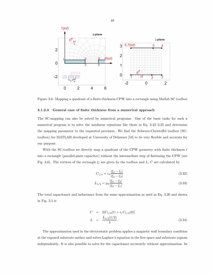
48
0 2 4 6
-2
0
2
-2 0 2
0
1
2
3
1 2
3 4
5
Inf
Inf
1 2 3
45Inf
EH
EH
z-plane
ξ-plane
s g
7( )
6( )
6,7( )
Figure 3.6: Mapping a quadrant of a finite-thickness CPW into a rectangle using Matlab SC toolbox
3.1.2.3 General case of finite thickness from a numerical approach
The SC-mapping can also be solved by numerical programs. One of the basic tasks for such a
numerical program is to solve the nonlinear equations like those in Eq. 3.22–3.25 and determine
the mapping parameter to the requested precision. We find the Schwarz-Christoffel toolbox (SC-
toolbox) for MATLAB developed at University of Delaware [53] to be very flexible and accurate for
our purpose.
With the SC-toolbox we directly map a quadrant of the CPW geometry with finite thickness t
into a rectangle (parallel-plate capacitor) without the intermediate step of flattening the CPW (see
Fig. 3.6). The vertices of the rectangle ξi are given by the toolbox and L, C are calculated by
C1/4 = ǫ0|ξ3 − ξ1||ξ4 − ξ3|
(3.32)
L1/4 = µ0|ξ4 − ξ3||ξ3 − ξ1|
. (3.33)
The total capacitance and inductance from the same approximation as used in Eq. 3.30 and shown
in Fig. 3.5 is
C = 2[C1/4(t) + ǫrC1/4(0)]
L =L1/4(t/2)
4. (3.34)
The approximation used in the electrostatic problem applies a magnetic wall boundary condition
at the exposed substrate surface and solves Laplace’s equation in the free space and substrate regions
independently. It is also possible to solve for the capacitance accurately without approximation. In

49
0 0.2 0.4 0.6 0.8 1 1.2
-0.4
-0.2
0
0.2
0.4
0.6
(a)
−0.04
−0.03
−0.02
−0.01
0
0.01
0.02
0.03
(b)
Figure 3.7: Calculating the exact capacitance of a CPW by solving Laplace’s equation in the W-plane
order to do this, we first map the right-hand-side half of the CPW into a parallel plate capacitor
partially filled with dielectric (see Fig. 3.7). Then we solve Laplace’s equation faithfully in the
parallel-plate structure by the partial differential equation (PDE) toolbox of Matlab. The PDE
toolbox internally implements the finite element method (FEM) and is capable of solving equations
of the general type [54]
−∇ · (c∇Φ) + aΦ = f. (3.35)
The equation compatible with PDE toolbox and appropriate for our electrostatic problem is
∇ · [ǫ(σ, η)∇Φ(σ, η)] = 0 (3.36)
which comes from one of Maxwell’s equations: ∇ · ~D = 0. ǫ(σ, η) is set to 1 (vertices in blue in
Fig. 3.7(b)) or ǫr (vertices in red in Fig. 3.7(b)) depending on whether (σ, η) maps to a point (x,y)
in the free space region or the substrate region in Fig. 3.7(a). The boundary conditions Φ = 1 and
Φ = 0 are applied on the left and right parallel plates, and ∂Φ∂v = 0 on both the top and bottom
edges of the rectangle. A typical solution of Φ is shown in Fig. 3.7(b). The difference between Φ
as compared to the solution of parallel plates fully filled with dielectric is plotted in Fig. 3.7(b). As
we can see, the former differs from the latter only in the air-substrate interface region. From the
solution Φ, the total electric energy we is calculated and the capacitance is derived.
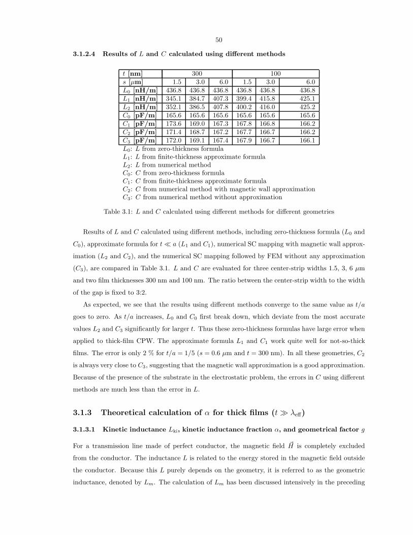
50
3.1.2.4 Results of L and C calculated using different methods
t [nm] 300 100s [µm] 1.5 3.0 6.0 1.5 3.0 6.0L0 [nH/m] 436.8 436.8 436.8 436.8 436.8 436.8L1 [nH/m] 345.1 384.7 407.3 399.4 415.8 425.1L2 [nH/m] 352.1 386.5 407.8 400.2 416.0 425.2C0 [pF/m] 165.6 165.6 165.6 165.6 165.6 165.6C1 [pF/m] 173.6 169.0 167.3 167.8 166.8 166.2C2 [pF/m] 171.4 168.7 167.2 167.7 166.7 166.2C3 [pF/m] 172.0 169.1 167.4 167.9 166.7 166.1L0: L from zero-thickness formulaL1: L from finite-thickness approximate formulaL2: L from numerical methodC0: C from zero-thickness formulaC1: C from finite-thickness approximate formulaC2: C from numerical method with magnetic wall approximationC3: C from numerical method without approximation
Table 3.1: L and C calculated using different methods for different geometries
Results of L and C calculated using different methods, including zero-thickness formula (L0 and
C0), approximate formula for t≪ a (L1 and C1), numerical SC mapping with magnetic wall approx-
imation (L2 and C2), and the numerical SC mapping followed by FEM without any approximation
(C3), are compared in Table 3.1. L and C are evaluated for three center-strip widths 1.5, 3, 6 µm
and two film thicknesses 300 nm and 100 nm. The ratio between the center-strip width to the width
of the gap is fixed to 3:2.
As expected, we see that the results using different methods converge to the same value as t/a
goes to zero. As t/a increases, L0 and C0 first break down, which deviate from the most accurate
values L2 and C3 significantly for larger t. Thus these zero-thickness formulas have large error when
applied to thick-film CPW. The approximate formula L1 and C1 work quite well for not-so-thick
films. The error is only 2 % for t/a = 1/5 (s = 0.6 µm and t = 300 nm). In all these geometries, C2
is always very close to C3, suggesting that the magnetic wall approximation is a good approximation.
Because of the presence of the substrate in the electrostatic problem, the errors in C using different
methods are much less than the error in L.
3.1.3 Theoretical calculation of α for thick films (t ≫ λeff)
3.1.3.1 Kinetic inductance Lki, kinetic inductance fraction α, and geometrical factor g
For a transmission line made of perfect conductor, the magnetic field ~H is completely excluded
from the conductor. The inductance L is related to the energy stored in the magnetic field outside
the conductor. Because this L purely depends on the geometry, it is referred to as the geometric
inductance, denoted by Lm. The calculation of Lm has been discussed intensively in the preceding

51
H
E
zE
Figure 3.8: ~E field and ~H field near the surface of a thick superconducting CPW.
section of this chapter.
For a superconducting transmission line, the ~H field extends into the superconductor by a dis-
tance given by the penetration depth. In this case, the supercurrent flowing in this penetrated
layer carries a significant amount of kinetic energy of the Cooper pairs, which will also contribute
to L. Because this energy depends on the penetration depth which changes with temperature and
quasi-particle density, we usually write the total inductance L as a sum of two parts, a fixed part
L0 and a variable part L1.
It can be shown that L0 ≈ Lm, because the magnetic field outside the superconductor is usually not
too much different from that of a perfect conductor and has little dependence on the penetration
depth. L1 is what we usually refer to as the kinetic inductance Lki.2 The total inductance can now
be written as
L = L0 + Lki ≈ Lm + Lki. (3.37)
The kinetic inductance fraction α is defined as the ratio of the kinetic inductance Lki to the total
inductance L
α =Lki
L. (3.38)
In MKIDs, a large α means a large fraction of the inductance is able to change with the quasi-particle
density, which usually means a more responsive detector.
Fig. 3.8 shows the ~E and ~H field inside and outside a thick superconducting CPW line. Inside
the superconductor, ~H and ~J are zero everywhere except in a surface layer of thickness λeff . Outside
2Strictly speaking, besides the kinetic energy of the Cooper pairs, the magnetic energy stored in the penetratingmagnetic field also contributes to the variable inductance L1. In the thick film case, these two contributions arecomparable, while in the thin film case, the kinetic energy of Cooper pairs dominates over the magnetic energy.Throughout this thesis, we do not discriminate L1 and Lki.

52
the superconductor, the fields are close to a TEM mode, except the ~E field has a small longitudinal
component Ez, giving rise to a small component of Poynting vector ~S directed normally into the
superconductor surface. This normal component delivers complex power (per unit length) into the
superconductor, which is calculated by∫C~E∗ × ~Hdl =
∫C E
∗z · H‖dl, where the integral is along
the surface contour C of the superconductor in the cross-sectional plane. On the other hand, the
dissipation and stored magnetic energy inside the superconductor are represented by 12RI
2 and
12LkiI
2, respectively, in the transmission line model. According to the Poynting theorem,
1
2RI2 = Re[
∫
CE∗
z ·H‖dl] (3.39)
1
2ωLkiI
2 = Im[
∫
CE∗
z ·H‖dl]. (3.40)
With the relationship between Ez and H‖ given by the surface impedance
Zs =Ez
H‖= Rs + jωLs. (3.41)
We finally derive
R = gRs (3.42)
Lki = gLs = gµ0λeff (3.43)
where
g =
∫C H
2‖dl
I2(3.44)
Eq. 3.44 shows that the kinetic inductance is related to the effective penetration depth λeff by
a factor g, which depends only on the geometry. The calculation of λeff is discussed in great detail
in Chapter 2. The calculation of the geometrical factor g requires the evaluation of the contour
integral of H2‖ . As discussed at the beginning of this chapter, H‖ can be derived by treating the
superconductor as a perfect conductor and solving the Laplace’s equation outside. This allows us to
use the same conformal mapping technique as used in the calculation of L and C.
3.1.3.2 Approximate formula of g under the condition of t≪ a
The contour integral of H2‖ in Eq. 3.44 diverges for a zero-thickness CPW, because a 1/x type of
singularity will be encountered at the edges of center strip and ground planes. For finite thickness
CPW, a 1/√x type of singularity will be encountered instead, which is integrable.
To evaluate the integral, we use the same two-step SC-mapping as used in Section 3.1.2.3: the

53
finite-thickness CPW in the Z-plane is first mapped into a zero-thickness CPW in the W -plane
by Eq. 3.21, which is then mapped into a parallel-plate structure in the ξ-plane by Eq. 3.12. It’s
most convenient to work on the integral in the W−plane. Assume a uniform magnetic field H = 1
between the parallel plates in the ξ-plane. The magnetic field H‖ in the W -plane and Z-plane are
|dξ/dw| and |dξ/dz| = |dξ/dw| / |dz/dw|, respectively. The current on the center strip I and the
geometrical factor g can be written as
I = 4
∫ u1
0
∣∣∣∣dξ
dw
∣∣∣∣ dw (3.45)
g =4
I2
∫ u1
0
+
∫ ∞
u2
[∣∣∣∣dξ
dw
∣∣∣∣ /∣∣∣∣dz
dw
∣∣∣∣]2 ∣∣∣∣
dz
dw
∣∣∣∣ dw (3.46)
with
∣∣∣∣dξ
dw
∣∣∣∣ =1∣∣∣
√(w2 − u2
1)(w2 − u2
2)∣∣∣
(3.47)
∣∣∣∣dz
dw
∣∣∣∣ =∣∣∣∣∣
√(w2 − u′21 )(w2 − u′22 )√(w2 − u2
1)(w2 − u2
2)
∣∣∣∣∣ . (3.48)
In the case of t≪ a, approximate solutions for u1, u′1, u2, u
′2 are available (see Eq. 3.27). Using
the lowest-order approximations: u1 = a, u′1 = a− 2t/π, u2 = b, u′2 = b+ 2t/π, a formula of g has
been derived by Collins[55]
g = gctr + ggnd
gctr =1
4aK2(k)(1 − k2)
[π + log
4πa
t− k log
1 + k
1 − k
]
ggnd =k
4aK2(k)(1 − k2)
[π + log
4πb
t− k log
1 + k
1 − k
](3.49)
where gctr and ggnd are the contribution from the center strip and the ground planes, respectively,
and k = a/b as before. This formula is estimated to be accurate to within 10 percent for t < 0.05a
and k < 0.8.
3.1.3.3 Numerical calculation of g for general cases
The geometrical factor g can be evaluated numerically with the help of SC-toolbox. To do this, one
must first determine the values of the mapping parameters of u1, u′1, u2, u
′2 using the SC-toolbox.
With these parameters available, the integrals in Eq. 3.46 can be evaluated numerically.

54
t [nm] 300 200 100s [µm] 0.6 3 6 0.6 3 6 0.6 3 6Lm [nH/m] 255.7 387.7 408.7 309.4 401.3 416.7 363.2 416.7 425.5g [µm−1] 1.525 0.391 0.214 1.633 0.4127 0.2249 1.819 0.4498 0.2434Lki [nH/m] 95.81 24.57 13.45 102.6 25.93 14.13 114.3 28.26 15.29α 0.2726 0.0596 0.03186 0.2491 0.06069 0.0328 0.2393 0.06351 0.03469
Table 3.2: Lm, g, Lki, and α calculated from the approximate formula Eq. 3.49. λeff = 50 nm isassumed in the calculation.
t [nm] 300 200 100s [µm] 0.6 3 6 0.6 3 6 0.6 3 6Lm [nH/m] 280.5 386.5 407.8 315.9 400.2 416 362.6 416 425.2g [µm−1] 1.209 0.3673 0.2066 1.385 0.3945 0.2193 1.655 0.4385 0.24Lki [nH/m] 75.98 23.08 12.98 86.99 24.79 13.78 104 27.55 15.08α 0.2132 0.05635 0.03085 0.2159 0.05832 0.03206 0.2229 0.06212 0.03426
Table 3.3: Lm, g, Lki, and α calculated from the numerical method. λeff = 50 nm is assumed in thecalculation.
3.1.3.4 A comparison of g calculated using different methods
The geometrical factor g, the kinetic inductance fraction α, as well as the geometric inductance Lm
and the kinetic inductance Lki are calculated using the two methods and are compared in Table 3.2
and 3.3. We see that the approximate formula of g gives less than 10% error for t/a < 0.1. We also
find that Lki increases as t or s decreases. Furthermore, g scales as 1/s. This is because H‖ scales
as 1/s while the integration interval scales as s (Eq. 3.44).
3.1.4 Theoretical calculation of α for thin films (t < λeff)
For thin films with t < λeff , the geometrical factor g and the kinetic inductance Lki can no longer
be evaluated from the contour integral of H‖ that is derived for a perfect conductor. The reason has
been discussed at the beginning of this chapter. There, we also show that in this case the vector
potential Az satisfies the Laplace equation outside the superconductor and the London equation
inside the superconductor, as given by
∇2 ~A =
1λ2L
~A , inside the superconductor
0, outside the superconductor.. (3.50)
A numerical program “induct” developed by Chang [56] is useful in this case. The program uses
a variational method to find the current distribution in superconducting strips and calculates the
inductance by minimizing the total magnetic and kinetic energy. It can be shown that the variational
method used in “induct” is equivalent to solving the equations 3.50. “Induct” takes one parameter,
the London penetration depth (effective) λL, and outputs the total inductance L. By comparing
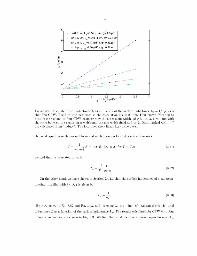
55
0 0.5 1 1.5 2 2.5 3 0
1
2
3
4
5
6
Ls = 1/σ
2 t (pH/sq)
L (µ
H/m
)
s=0.6 µm, Lm
=0.52 µH/m, g= 1.8/µm
s= 1.5 µm, Lm
=0.49 µH/m, g= 0.74/µm
s= 3 um, Lm
=0.47 µH/m, g= 0.39/µm
s= 6 µm, Lm
=0.46 µH/m, g= 0.2/µm
Figure 3.9: Calculated total inductance L as a function of the surface inductance Ls = 1/σ2t for athin-film CPW. The film thickness used in the calculation is t = 20 nm. Four curves from top tobottom correspond to four CPW geometries with center strip widths of 0.6, 1.5, 3, 6 µm and withthe ratio between the center strip width and the gap width fixed at 3 to 2. Data marked with “+”are calculated from “induct”. The four lines show linear fits to the data.
the local equation in the normal form and in the London form at low temperatures,
~J =1
iωµ0λ2L
~E = −iσ2~E, (σ1 ≪ σ2 for T ≪ Tc) (3.51)
we find that λL is related to σ2 by
λL =
√1
ωµ0σ2. (3.52)
On the other hand, we have shown in Section 2.4.1.3 that the surface inductance of a supercon-
ducting thin film with t < λeff is given by
Ls =1
σ2t(3.53)
By varying σ2 in Eq. 3.52 and Eq. 3.53, and inserting λL into “induct”, we can derive the total
inductance L as a function of the surface inductance Ls. The results calculated for CPW with four
different geometries are shown in Fig. 3.9. We find that L almost has a linear dependence on Ls,

56
which allows us to extend the thick-film formula
L = Lm + gLs (3.54)
to the thin film case. The equivalent geometrical inductance Lm and geometrical factor g can be
determined from the intercept and slope of a linear fit to the data. The linear fits are indicated by
the solid lines in Fig. 3.9, with the derived values of Lm and g listed in the legend. The equivalent
kinetic inductance Lki and kinetic inductance fraction α for the thin film case are still given by
Lki = gLs
α =gLs
Lm + gLs(3.55)
Thus, we have unified formulation for both the thick film and thin film cases.
For a specific CPW, the relevant quantities (L, Lm, Lki, g, and α) can be derived using the
following procedures:
1. Calculate the total inductance L as a function of the surface inductance Ls for the specific
film thickness t, and from a linear fit, derive Lm and g;
2. Measure the sheet resistance of the film above its Tc (e.g., at 4 K for Al films), from which
derive σn;
3. Calculate σ2(ω, T ) from the formula of σ2/σn derived in Chapter 2 (Eq. 2.92);
4. Insert σ2 into Eq. 3.53, and from Eq. 3.54 and Eq. 3.55 derive Lki and α.
3.1.5 Partial kinetic inductance fraction
It is often the case that the quasiparticles are only generated in the center strip of CPW instead of the
whole superconducting film. In this situation, although the entire superconducting film contributes
to Lki, only the center strip where quasiparticle density has a change δnqp contributes to δLki. Thus
we define a partial kinetic inductance fraction α∗ as
α∗ =L∗
ki
L=L∗
ki
Lkiα (3.56)
where L∗ki is the partial kinetic inductance contributed from the center strip of the CPW. In the
thick film case (t ≫ λeff), L∗ki is calculated by

57
s [µm] 0.6 3 6 5 5 5g [µm] 0.4 2 4 1 2 3r1 0.7309 0.7244 0.7224 0.6133 0.6713 0.7118r2 0.6528 0.6986 0.7074 0.5911 0.6513 0.6939r1: ratio of α∗/α from Eq. 3.49r2: ratio of α∗/α from numerical method
Table 3.4: Ratio of α∗/α calculated using the two methods. A film thickness of t = 200 nm is usedin these calculations.
s [µm] 3 5g [µm] 2 2λL [nm] 100 150 200 100 150 200t = 40 nm 0.8174 0.858 0.8863 0.7613 0.8066 0.8412t = 60 nm 0.7978 0.8368 0.8664 0.7412 0.7821 0.8162t = 100 nm 0.7762 0.8107 0.8395 0.7192 0.754 0.7851
Table 3.5: Ratio of α∗/α calculated using “induct” program
L∗ki = g∗Ls
g∗ =
∫C∗ H
2‖dl
I2(3.57)
where the contour C∗ only runs along the surface of the center strip. In Eq. 3.49 we already give
an approximate formula for g∗, and numerical evaluation of g∗ is also straightforward. The ratios of
L∗ki/Lki (or α∗/α) evaluated from both the approximate formula and numerical method for a number
of geometries are listed in Table 3.4. We can see that the center strip accounts for more than half
of the kinetic inductance. As t/a → 0, the ratio approaches a constant L∗ki/Lki → 1/(1 + k) = 0.7
for CPW geometries with center-strip-to-gap ratio of 3:2, according to Eq. 3.49.
In the thin film case (t < λeff), α∗/α can still be calculated by using the “induct” program. The
“induct” program allows users to assign different London penetration depths to the center strip and
the ground planes. We first calculate the total inductance L and its increment δL by assigning both
the center strip and the ground planes with the actual λL and λL + δλL. Then we calculate the
partial inductance increment δL∗ by only increasing the London penetration depth of the center
strip to λL + δλL while keeping the ground planes at λL. The ratio of δL∗/δL yields the ratio of
α∗/α. The ratios of δL∗/δL are calculated for a number of combinations of geometry, thickness, and
London penetration depth, and are listed in Table 3.5. We find that for these geometries the ratios
are between 80 % to 90 %, and are higher than the thick film case.

58
3.2 Experimental determination of α
In this section, we describe an experimental method to determine the kinetic inductance fraction α
of a superconducting CPW.
3.2.1 Principle of the experiment
lc lr
in
outfe
edline
couple
r
resonator
Figure 3.10: Coupler structure of the α-test device
The resonant frequency fr of a quarter–wave resonator of length lr is given by
fr =1
4lr√LC
. (3.58)
According to Eq. 3.58 and Eq. 3.37, a straightforward way of determining α is to compare the
measured resonance frequency of a superconducting CPW resonator f scr , with the calculated resonant
frequency fmr of the same resonator assuming only the magnetic inductance Lm:
α = 1 − (f sc
r
fmr
)2. (3.59)
This method, however, is only accurate for CPW with large α, because the relative error in Eq. 3.59
is:σα
α= 2
1 − α
α
√(σfm
r
fmr
)2 + (σfsc
r
f scr
)2. (3.60)
For example, if f scr or fm
r has an relative error of 1%, the relative error in α will be 6% for α = 25%
which is acceptable, and 98% for α = 2% which is too large to be useful.
For a CPW geometry with small α, we resort to the temperature dependence of the resonant

59
Res# Group# s [µm] Lc [µm] Lr [mm] fmr [GHz] Qc
0 1 0.6 168.60 4558.42 6.466 1.0107E+051 1 0.6 168.60 4533.42 6.500 1.0000E+052 1 0.6 168.60 4508.42 6.535 9.8937E+043 2 1.5 130.45 4408.41 6.713 2.0222E+054 2 1.5 130.45 4383.41 6.750 2.0000E+055 2 1.5 130.45 4358.41 6.788 1.9779E+056 3 3.0 156.56 4180.82 6.960 1.0116E+057 3 3.0 156.56 4155.82 7.000 1.0000E+058 3 3.0 156.56 4130.82 7.041 9.8844E+049 4 6.0 173.75 4004.95 7.163 6.8670E+04
10 4 6.0 148.75 4004.95 7.206 1.0886E+0511 4 6.0 123.75 4004.95 7.250 2.0000E+0512 4 6.0 123.75 3979.95 7.294 1.9759E+0513 4 6.0 123.75 3954.95 7.339 1.9519E+0514 5 24.0 263.41 3713.70 7.453 2.0254E+0415 5 24.0 263.41 3663.70 7.548 1.9748E+04
Table 3.6: Design parameters of the α-test device. fmr is calculated assuming a film thickness of
200 nm.
frequency fr and quality factor Qr (see Eq. 2.54):
δfr(T )
fr=
fr(T ) − fr(0)
fr(0)= −α
2
δXs(T )
Xs
δ1
Qr(T )=
1
Qr(T )− 1
Qr(0)= α
Rs(T )
Xs. (3.61)
Because the temperature dependence of the surface impedance is an intrinsic property of the su-
perconductor, Xs(T ) and Rs(T ) are common for resonators of all geometries made from the same
superconducting film. The ratio of δfr/fr or δ(1/Qr) between two CPW geometries, with the
common temperature dependence canceled out, gives the ratio of α:
αi
αj=
(δfr/fr)i
(δfr/fr)j=δ(1/Qr)i
δ(1/Qr)j. (3.62)
If αi is large and can be determined with a good accuracy from Eq. 3.59, the small αj can also be
determined with fairly good accuracy by scaling αi with the ratio given by Eq. 3.62.
3.2.2 α-test device and the experimental setup
For this experiment, we designed two α-test devices which are made of Al films with two different
thicknesses: 200 nm and 20 nm. In each device, an Al film was deposited on a silicon substrate
and patterned into 16 CPW quarter-wavelength resonators with 5 different geometries. As shown in
Fig. 3.10, each resonator has a coupler of length lc and a common center-strip width of 6 µm, which
capacitively couples the resonator body to the feedline for readout. The coupler is then widened (or

60
narrowed) into the resonator body, with center-strip widths sr of 0.6 µm, 1.5 µm, 3 µm, 6 µm, or
24 µm, and a length lr. The ratio between center strip width s and the gap g in both the coupler
and the resonator body section is fixed to 3:2, to maintain a constant impedance at Z0 ≈ 50 Ω.
The relevant design parameters of the α-test device are listed in Table 3.2.2. Because the smaller
geometries are expected to have larger α, they are designed to have smaller fmr . This guarantees
the actual resonance frequencies f scr are always in a fixed order easy to recognize, with smaller
geometries at lower frequencies regardless of the film thickness.
The device is mounted in a dilution fridge and cooled down to T as low as 100 mK. A microwave
synthesizer is used to excite the resonators. The signal transmitted past the resonator is amplified
with a cryogenic HEMT amplifier and compared with the original signal using an IQ-mixer. As
the excitation frequency f is swept through the resonance, the I-Q output from the IQ-mixer, after
corrections, gives the complex transmission S21 through the device and HEMT. The readout system
used in this experiment is described in more detail in Section 5.2 and shown in Fig. 5.1. The
resonance frequency fr is obtained by fitting the complex S21 data to its theoretical model. The
IQ-mixer correction and resonance curve fitting are given in the Appendix E and F.
3.2.3 Results of 200 nm Al α-test device (t ≫ λeff and t ≪ a)
The 200 nm device was cooled in the dilution fridge and Tc was measured to be 1.25 K. All the 16
resonators were observed.
3.2.3.1 α of the smallest geometry
We first measured the resonant frequency and quality factor of all the resonators at 150 mK. α
are immediately calculated from Eq. 3.59 for each resonator and the group mean value is listed in
Table 3.7 in the column “α1”. We will only take α11 = 27.6% of group 1 as a reliable value and
abandon the rest, based on the previous discussion.
3.2.3.2 Retrieving values of α from fr(T ) and Qr(T )
α of the remaining four geometries are determined from the temperature sweep data. δfr(T )/fr and
δ(1/Qr) for all the resonators are measured from 150 mK to 480 mK in steps of 10 mK and plotted
in Fig. 3.11(a) and Fig 3.11(b) . In both plots, the curves fall onto 5 trajectories corresponding to
the 5 geometries. We normalize them by the value of group-1. The normalized curves appear to be
flat in the temperature range between 220 mK and 300 mK (see Fig. 3.12), where the ratios αi/α1
are retrieved. The ratios as well as the values of αi scaling down from α1 are listed in Table 3.7 in
the two columns “αi/α1” and “α2”.
The ratio of αi/α1 can also be derived by fitting δfr/fr and δ(1/Qr) to Eq. 3.61, with δXs/Xs

61
0.15 0.2 0.25 0.3 0.35 0.4 0.45−10
−8
−6
−4
−2
0
x 10−5
T (K)
δfr/f r
0123456789101112131415
(a)
0.15 0.2 0.25 0.3 0.35 0.4 0.45−1
0
1
2
3
4
5
6x 10
−5
T (K)
δ(1/
Q)
(b)
Figure 3.11: Measured δfr/fr and δ(1/Qr) as a function of T from the 200 nm α-test device(a)Plot of δfr/fr vs. T (b)Plot of δ(1/Qr) vs. T
0.2 0.22 0.24 0.26 0.280
0.1
0.2
0.3
0.4
0.5
0.6
0.7
0.8
0.9
1
1.1
1.2
T (K)
1.00
0.43
0.23
0.13
0.039
αi/α
1
Figure 3.12: δfr/fr normalized by group-1 from the 200 nm α-test device

62
0 0.002 0.004 0.006 0.008 0.01 0.012 0.014−1
−0.8
−0.6
−0.4
−0.2
0x 10
−4
δ f r/f r
δ Xs/X
s
g1g2g3g4g5
(a)
0 1 2 3 4
x 10−3
0
1
2
3
4
5
6x 10
−5
δ (1
/Q)
Rs/X
S
g1g2g3g4g5
(b)
Figure 3.13: Fitting (a)δfr/fr with δXs/Xs and (b)δ(1/Qr) with Rs/Xs from the 200 nm α-testdevice
group# α1 αi/α1 α2 α3 α4 α5
1 27.6% 1.000 27.6% 27.6% 27.6% 30.8%2 12.3% 0.430 11.9% 12.6% 13.1% 14.5%3 4.3% 0.230 6.3% 7.0% 7.2% 7.8%4 0.3% 0.130 3.6% 4.1% 4.0% 4.2%5 -6.5% 0.039 1.1% 1.3% 1.2% 1.2%
Table 3.7: Results from the 200 nm α-test device
α1: α from Eq. 3.59αi/α1: α ratio between the ith group and the group 1α2: α from scaling the largest alpha with αi/α1
α3: α from fitting δfr/fr to δXs/Xs
α4: α from fitting δ(1/Qr) to Rs/Xs
α5: α from a numerical calculation of g and λ ≈= 64 nm from “surimp”
and Rs/Xs calculated from Martis-Bardeen theory by our “surimp” program described in Chapter
2. As for the five material-dependent parameters required by “surimp”, we take values of vf and
λL from reference[40], Tc = 1.25 K, and l = 200 nm (limited by the film thickness). The parameter
∆(0)/kbTc is chosen such that the fitting yields 27.6% for the smallest 0.6–0.4 geometry. Once
determined, the same five parameters are used to fit for the other four geometries. The results are
listed in Table 3.7 in the column “α3” and “α4”. We see that “α3” and “α4” agree with “α2”. The
advantage of the fitting approach (α3, α4) over the direct ratio approach (α2) is that the former
takes into account of the frequency dependence of the surface impedance which does not cancel
completely in Eq. 3.62 between two resonators.
3.2.3.3 Comparing with the theoretical calculations
The experimental results of α are compared with the theoretical calculations. The kinetic inductance
fraction can be calculated from Eq. 3.44 and Eq. 3.43 because the film thickness is several times

63
larger than the penetration depth. With λeff = 64 nm calculated from “surimp”, calculated values
of α are listed in Table 3.7 in the column “α5”. We find a good agreement, within 10%, between
the theoretical results and the experimental results.
3.2.4 Results of 20 nm Al α-test device (t < λeff)
The 20 nm α-test device was cooled in a dilution fridge in another cooldown. Tc was measured to
be 1.56 K. 14 out of the 16 resonators showed up (Res 2 and Res 11 fail to show up).
3.2.4.1 α of the smallest geometry
We measured the resonant frequency and quality factor of all the 14 resonators at 120 mK. α
calculated from Eq. 3.59 are listed in Table 3.8 under column “α1”. We see that α of this 20 nm
device is significantly larger than the 200 nm device. Even the largest geometry gives an α over
20%. Thus the values of α1 derived from Eq. 3.59 are all reliable.
3.2.4.2 Retrieving values of α from fr(T )
δfr/fr as a function of T are measured between 110 mK and 575 mK in steps of 15 mK and plotted
in Fig. 3.14. Curves for the 14 resonators still fall onto five trajectories. The quality factors are
also measured which appear to be very low. We were unable to distinguish trajectories between
geometric groups from the δ(1/Qr) curves. So we proceed only with the δfr/fr data. The results
from both the direct ratio approach and the fitting approach are shown in Fig. 3.15 and Fig. 3.16,
and are listed in Table 3.8 under columns “α2” and “α3”. The parameters used in the fits are: Tc=
1.56 K, l=20 nm, vf = 1.34 × 10⁶ m/s, λL = 15.4 nm, and ∆0/kbTc = 1.71. We can see that the
values of α2 and α3 are notably smaller compared to α1, for which we do not have an explanation
yet.
0.2 0.3 0.4 0.5 0.6−5
−4
−3
−2
−1
0
1x 10
−3
T (K)
δ f r/f r
0234567891012131415
Figure 3.14: Measured δfr/fr as a functionof T from the 20 nm Al device
0.3 0.35 0.4 0.450
0.1
0.2
0.3
0.4
0.5
0.6
0.7
0.8
0.9
1
1.1
1.2
T (K)
α i/α1
1.00
0.77
0.56
0.43
0.16
Figure 3.15: δfr/fr normalized by group 1from the 20 nm device

64
0 0.005 0.01 0.015 0.02 0.025 0.03
−4
−3
−2
−1
0
x 10−3
δ f r/f r
δ Xs/X
s
g1g1−fitg2g2−fitg3g3−fitg4g4−fitg5g5−fit
Figure 3.16: Fitting δfr/fr with δXs/Xs from the 20 nm device
g# α1 αi/α1 α2 α3 α6
1 89.3% 1.000 89.3% 89.3% 88.3%2 76.5% 0.770 68.7% 70.2% 75.6%3 62.7% 0.560 50.0% 51.6% 61.8%4 45.3% 0.430 38.4% 41.0% 46.4%5 20.6% 0.160 14.3% 16.8% 20.2%
Table 3.8: Results from the 20 nm α-test device
α6: α calculated from “induct” program with λL = 165 nm. Other symbols same as in Table 3.7.
3.2.4.3 Comparing with the theoretical calculations
Since the thickness 20 nm is less than the effective penetration depth, it is appropriate to calculate
α from “induct” program, instead of surface integral method. α calculated from “induct” program,
assuming a effective London penetration depth of λL = 165 nm, are listed in Table 3.8 in the column
“α6”. Unfortunately, the sheet resistance of the film at 4 K was not measured for this device and
λL can not be verified from the procedures described in Section 3.1.4.
3.2.5 A table of experimentally determined α for different geometries and
thicknesses.
The values of α determined from the two α-test devices described in this section and from another
40 nm geometry-varying device are summarized in Table 3.9. This table is useful for a quick estima-
tion of α for geometries listed or close to those listed in the table. For example, the submm MKID,
with a 6 µm width center strip, a 2 µm wide gap, and a 60 nm thick Al film, is estimated to have a
kinetic inductance fraction around 20%.

65
s [µm] \ t [nm] 200 40 200.6 27.6% 89.3%1.5 12.6% 76.5%
3 7% 45% 62.7%5 26%6 4.1% 45.3%
10 17%24 1.3% 20.6%
Table 3.9: Summary of experimentally determined α for different center-strip widths and thicknesses.Values of α are reported using α1 for 20 nm and 40 nm devices, and α3 for 200 nm device.

66
Chapter 4
Analysis of the resonator readoutcircuit
In this chapter, we discuss the resonator readout circuit. The basic question to be answered is: if
the kinetic inductance of the superconducting resonator has a change δLki due to a change in the
quasiparticle density δnqp, what will be the change in the phase and amplitude of the microwave
output signal?
We begin with an introduction of the basics of a quarter-wave transmission line resonator. Then
we present a network model of a resonator capacitively coupled to a feedline. To be general, we
assume the transmission line resonator is terminated by a small impedance Zl instead of being
shorted. From the network model, we derive the responsivity of MKID both for Zl = 0 case and
Zl 6= 0 case. The Zl = 0 case corresponds to the simple short-circuited λ/4 resonator and the
Zl 6= 0 case corresponds to the hybrid resonator, which has a short sensor strip section near the
short-circuited end that is made from a different type of superconductor or a different geometry
from the rest of the resonator. For the hybrid resonator, both the static and dynamic response are
discussed.
4.1 Quarter-wave transmission line resonator
4.1.1 Input impedance and equivalent lumped element circuit
A short-circuited CPW transmission line of length λ/4 (see Fig. 4.1(a)) makes a simple while useful
microwave resonator[57]. According to the transmission line theory, the input impedance of a shorted
transmission line of length l is
Zin = Z0 tanh(α+ jβ)l = Z01 − j tanhαl cotβl
tanhαl − j cotβl(4.1)

67
in
0
0
cos2
m
xV
l
sin
2m
xI
l
(a)
L RC
inZ
inV
(b)
Figure 4.1: A short-circuited λ/4 transmission line and its equivalent circuit. (a) Illustration of ashort-circuited λ/4 resoantor. The voltage and current distributions show standing wave patterns.(b) The equivalent RLC parallel resonance circuit, valid near resonance
where
γ = α+ jβ =√
(R+ jωL)(jωC) (4.2)
is the complex propagation constant, and
Z0 =
√L
C(4.3)
is the characteristic impedance of the transmission line. Here L, C, and R are the distributed
inductance, capacitance, and resistance of the transmission line.
For a lossless line, α = 0 and
Zin = jZ0 tanβl. (4.4)
At the fundamental resonance frequency
ω0 =π
2l√LC
or f0 =1
4l√LC
(4.5)
we have
β0l =π
2, Zin = ∞. (4.6)

68
For a transmission line with small loss αl ≪ 1 at a frequency close to the resonance frequency
ω = ω0 + ∆ω, Eq. 4.1 approximately reduces to
Zin =Z0
αl + jπ∆ω/2ω0. (4.7)
Recall that the impedance of a parallel RLC circuit shown in Fig. 4.1(b) has the same form near
the resonance frequency
Zin =1
1/R+ 2j∆ωC. (4.8)
Thus a short-circuited transmission line of length λ/4 is equivalent to a parallel RLC resonance
circuit, with the equivalent lumped elements R, L, and C related to the distributed R, L, and C of
the transmission line by
R =2
l
L
RC, C =
l
2C, L =
8l
π2L. (4.9)
And the quality factor Q of the circuit is
Q =π
4αl= ω0
L
R. (4.10)
4.1.2 Voltage, current, and energy in the resonator
At the resonance frequency ω = ω0, the RMS voltage and current have standing-wave distributions
along the transmission line
V (x) = Vm cosπx
2l, I(x) = Im sin
πx
2l(4.11)
where Vm is the maximum voltage at the open end (x = 0) and Im is the maximum current at the
shorted end (x = l). Vm and Im are related by Vm = ImZ0. It follows that the electric energy,
magnetic energy and dissipation (per unit length) are
We(x) =1
2CV (x)2 =
1
2CV 2
m cos2πx
2l
Wm(x) =1
2LI(x)2 =
1
2LI2
m sin2 πx
2l
Pl(x) =1
2RI(x)2 =
1
2RI2
m sin2 πx
2l. (4.12)

69
The lumped-element relationships in Eq. 4.9 can also be derived by equating the total electric energy
and magnetic energy in the RLC tank circuit and in the transmission line resonator,
Total electric energy =1
2CV 2
in =1
2
∫ l
0
CV 2m cos2
πx
2ldx
Total magnetic energy =1
2
V 2in
ω20L
=1
2
∫ l
0
LI2m sin2 πx
2ldx
Total dissipation =1
2
V 2in
R=
1
2
∫ l
0
RI2m sin2 πx
2ldx (4.13)
which, by applying Vin = Vm and Eq. 4.5, leads to the same results as in Eq. 4.9.
4.2 Network model of a quarter-wave resonator capacitively
coupled to a feedline
feedline
to resonator
Lc
(a)
1 2
3
Z0 Z0
Zr
Cc
(b)
1 (Z0)
Zr
ZL
V1+
V2-
S21 2 (Z0)
3 (Zr)
A (Zr)
VA+
VA-
S31
S33
SAA
SA3
L
(c)
Figure 4.2: Network model of a λ/4 resonator capacitively coupled to a feedline. (a)The “elbow”coupler. (b) Equivalent lumped element circuit of the coupler. (c) A network model and the signalflow graph
The resonator readout circuit used in MKIDs consists of feedline, coupler, and λ/4 transmission

70
line resonator, which is shown in Fig. 4.2(a). Using the equivalent circuit of the coupler shown
in Fig. 4.2(b), and by considering the frequency dependent complex impedance of a shorted λ/4
transmission line (Eq. 4.7), Mazin[16] and Day[14] have derived the resonance condition for the
circuit. Here we present an alternative derivation from the network analysis approach.
4.2.1 Network diagram
Fig. 4.2(c) shows a diagram of the equivalent network model, as well as its signal flow graph. In this
diagram, the coupler is modeled by a 3-port network block with its port 3 connected to one end of
the λ/4 transmission line. To facilitate future discussions of the hybrid resonator design, we assume
the other end of the transmission line is terminated by a load impedance Zl. For the case of shorted
λ/4 resonator, we shall simply set Zl = 0. We assume that the feedline is a lossless transmission line
with characteristic impedance Z0, which may be different from the impedance Zr of the resonator
transmission line.
4.2.2 Scattering matrix elements of the coupler’s 3-port network
The scattering matrix of the coupler’s 3-port network can be easily derived from its equivalent
lumped element circuit (Fig. 4.2(b)), in which a coupling capacitor Cc weakly couples the resonator
to the feedline. Let δ0 = ωCcZ0 and δr = ωCcZr. For weak coupling (which is required by a high
Qr resonator), Cc is small and δ0, δr ≪ 1. Under these assumptions, the scattering matrix S is
given by1
S =
−jδ0/2 1 − jδ0/2 j√δ0δr
1 − jδ0/2 −jδ0/2 j√δ0δr
j√δ0δr j
√δ0δr 1 − 2jδr − 2δ2r − δrδ0
. (4.14)
We find the following general properties for Sij :
S21 ≈ 1 (4.15)
S31 = S13, S32 = S23 (4.16)
S31 = S32, S13 = S23 (4.17)
|S33| =√
1 − 2|S31|2. (4.18)
Eq. 4.15 states the fact that the direct transmission through the feedline is close to 1. Eq. 4.16 comes
from the reciprocity of the 3-port network. Because the dimension of the coupler is much smaller
1In the discussion that follows, S-parameters are normalized to the characteristic impedance of Z0 for port 1 andport 2, and Zr for port 3 and port A.

71
than the wavelength, port 1 and port 2 appear to be symmetric and Eq. 4.17 holds. Eq. 4.18 holds
because the 3-port network is lossless.
4.2.3 Scattering matrix elements of the extended coupler-resonator’s 3-
port network
We can extend the coupler’s 3-port network to include the λ/4 transmission line connected to port-3.
This can be easily done by shifting the reference plane of port-3 to the other end of the resonator,
to port A. The relevant scattering matrix elements are modified to
SA1 = S1A = SA2 = S2A = S31e−γl (4.19)
SAA = S33e−2γl (4.20)
where l ≈ λ/4 is the length of the transmission line section.
4.2.4 Transmission coefficient t21 of the reduced 2-port network
When port-A is terminated by the load impedance Zl, the whole circuit reduces to a 2-port network.
With the help of the signal flow graph, the total transmission from port 1 to port 2 can be written
as:
t21 = S21 +SA1ΓS2A
1 − ΓSAA= S21 +
S231
e2γl/Γ − S33(4.21)
where Γ is the reflection coefficient from the load
Γ =Zl − Zr
Zl + Zr. (4.22)
For the simple case that the λ/4 transmission line is shorted at port A, Γ = −1. In order to further
simplify Eq. 4.21, we first introduce a coupling quality factor Qc defined as:
Qc = 2πenergy stored in the resonator
energy leak from port 3 to port 1 and 2 per cycle=
π
2|S31|2. (4.23)
The relationship between Qc and S31 can be understood from a power flow point of view: during
each cycle the traveling wave inside the λ/4 resonator is reflected twice at port 3 and upon each
reflection a fraction |S13|2 of the stored energy leaks out to port 1 and port 2, respectively. As a
result, a total fraction 4|S13|2 of the energy leaks out of the resonator per cycle.
72
With Eq. 4.23, we find
S31 = j
√π
2Qc(4.24)
S33 ≈√
1 − 2|S31|2ejφ ≈ 1 − π
2Qc+ jφ, (φ << 1) (4.25)
where φ ≪ 1 because the wave is reflected from an open end of the transmission line at port 3.
Because of the small coupling capacitance Cc, the input impedance of port 3 is very high. Meanwhile,
the propagation constant γ is related to the distributed inductance L, capacitance C, and resistance
R by:
γ = α+ jβ = jβ(1 − j
2QTL) =
√(R+ jωL)(jωC) (4.26)
where
β = ω√LC (4.27)
QTL =ωL
R. (4.28)
QTL is the quality factor of the transmission line.
Define a quarter-wave resonance frequency fλ/4 as,
fλ/4 =1
4l√LC
. (4.29)
Under the condition that l ≈ λ/4 and Zl ≪ Zr, we have
−e2γl =≈ 1 +π
2QTL+ jπ
f − fλ/4
fλ/4(4.30)
1
−Γ=Zr + Zl
Zr − Zl≈ 1 + 2zl = 1 + 2rl + 2jxl = 1 +
π
2Ql+ 2jxl (4.31)
with
zl =Zl
Zr= rl + jxl, (|zl| ≪ 1) (4.32)
Ql =π
4rl(4.33)
where Ql is the quality factor associated with the dissipation in the load impedance.
73
With these relationships, Eq. 4.21 can now be reduced to
t21 = S21 +S2
31
e2γl/Γ − S33
= 1 −1
Qc
( 1Qc
+ 1QT L
+ 1Ql
) + 2j(f−fλ/4fλ/4
+ 2πxL − φ
π )
= 1 −Qr
Qc
1 + 2jQrf−fr
fr
(4.34)
where Qr is the total quality factor of the resonator given by
1
Qr=
1
Qc+
1
Qi=
1
Qc+
1
QTL+
1
Ql. (4.35)
Qi is the internal quality factor of the resonator which accounts for all the other loss channels (Ql,
QTL) than through coupling to the feedline (QC). The resonance frequency fr is given by
fr = fλ/4(1 +φ
π− 2xL
π). (4.36)
4.2.5 Properties of the resonance curves
For a simple shorted λ/4 resonator, we set Zl = 0 and the resonance frequency and quality factor
are given by
fr = fλ/4(1 +φ
π) (4.37)
1
Qr=
1
Qc+
1
Qi, Qi = QTL. (4.38)
According to Eq. 4.34, t21(f) is fully characterized by three parameters Qc, fr, Qr (or Qi). Qc
depends on the coupling capacitance Cc and is fixed for a certain coupler design. fr and Qi are
related to the transmission line parameters (R, L, C, and l) of the resonator.
The complex t21 as a function of f is plotted in Fig. 4.3(a). When f ≪ fr or f ≫ fr, t21 is
close to t21(∞) = 1 and the feedline is unaffected by the resonator. When f sweeps through the
resonance, t21 traces out a circle which is referred to as the resonance circle. At the resonance
frequency f = fr,
t21 = 1 − Q
Qc=
1/Qi
1/Qi + 1/Qc. (4.39)
The diameter of the circle is
d =Q
Qc=
1/Qc
1/Qi + 1/Qc. (4.40)

74
0.2
0.4
0.6
0.8
1
30
210
60
240
90
270
120
300
150
330
180 0
(a)
−5 0 5
0.4
0.5
0.6
0.7
0.8
0.9
1
f−fr [MHz]
|t 21|
|t21
(f)|
|t21
(fr)|
|t’21
(f)|
|t’21
(fr’)|
|t’21
(fr)|
(b)
−5 0 5−1.5
−1
−0.5
0
0.5
1
1.5
f−fr [MHz]
arg(
1−t 21
)
arg(1−t21
(f))
arg(1−t21
(fr))
arg(1−t’21
(f))
arg(1−t’21
(fr’))
arg(1−t’21
(fr))
(c)
Figure 4.3: Plot of t21(f) (solid line) and its variation t′21(f) (dashed line) due to a small change inδfr and δQr. (a) complex plot (b) magnitude plot (c) phase plot (with respect to t21(∞) = 1)

75
In the coupling Q limited case where Qc ≪ Qi, we find Q → Qc and d → 1, while in the internal
Q limited case where Qc ≫ Qi, we find Q → Qi and d → 0. In the critical coupling case we have
Qc = Qi and d = 1/2.
The magnitude of t21 as a function of f is plotted in Fig. 4.3(b). According to Eq. 4.34, |t21(f)|2
has a Lorentzian shape
|t21(f)|2 = 1 −1
Q2r− 1
Q2i
1Q2
r+ 4
(f−fr
fr
)2 . (4.41)
Again, when f ≫ fr or f ≪ fr, the transmission |t21| is close to 1; at the resonance frequency
f = fr, |t21| is at the minimum and the feedline is fully loaded by the resonator.
The phase angle θ of t21 with respect to the off-resonance point t21(∞) = 1 is plotted in
Fig. 4.3(c). θ equals half of the phase angle measured from the center of the circle. According
to Eq. 4.34, θ has the following profile
θ = − arctan2Qrf − fr
fr(4.42)
which changes from π/2 to −π/2 when f sweeps from f ≪ fr to f ≫ fr. We find that the slope
dθ/df is maximized at the resonance frequency f = fr.
The complex t21 can be measured with a vector network analyzer. The resonance parameters
Qc, fr, Q, and Qi can be obtained by fitting the t21 data to the theoretical models. There are at
least two different fitting methods: one can fit the magnitude |t21| to a Lorentzian profile according
to Eq. 4.41, or fit the phase angle θ to an “arctan” profile according to Eq. 4.42. Discussion on both
methods are given in Appendix E.
4.3 Responsivity of MKIDs I — shorted λ/4 resonator (Zl =
0)
If the distributed inductance and resistance of the superconducting transmission line have small
variations δL and δR, due to a change in the quasiparticle density δnqp, the variation in the resonance
frequency and quality factor are given by, according to Eq. 4.28, Eq. 4.36, and Eq. 3.37-3.43,
δfr
fr= −1
2
δL
L= −α
2
δLki
Lki= −α
2
δXs
Xs(4.43)
δ1
Qi=
δR
ω0L= α
δRs
Xs(4.44)
where Zs = Rs+jXs is the surface impedance and α is the kinetic inductance fraction. The variation
of t21 with the microwave frequency tuned to and fixed at the original resonance frequency fr is,
76
from Eq. 4.34,
δt21|f=fr =Q2
r
Qc(δ
1
Qi− 2j
δfr
fr) ≈ α
Q2r
Qc
δZs
|Zs|, (Rs ≪ Xs for T ≪ Tc). (4.45)
The relationship between δt21 and δnqp is, from Eq. 4.45, Eq. 2.80, and Eq. 2.100,
δt21 = α|γ|κQ2r
Qcδnqp (4.46)
where κ is the coefficient defined in Eq. 2.100.
Eq. 4.46 is appropriate for quasiparticles generated uniformly in the entire resonator, both in
the center strip and the ground planes. A change in the thermal quasi-particle density caused by
a change in the bath temperature will lead to a resonator response that is describable by Eq. 4.46.
In the photon detection applications, however, the quasiparticles are usually generated only in the
center strip, and so α in Eq. 4.46 should be replaced by the partial kinetic inductance fraction α∗.
We should also take into account the fact that the quasiparticles are usually generated near the
shorted end instead of the entire center strip. It can be derived from a modal analysis that the effect
to the resonance frequency and internal quality factor due to position dependent variations δL(x)
and δR(x) are weighted by the square of the current distribution in the resonator2:
δfr
fr= −1
l
∫ l
0
sin2 πx
2l
δL(x)
Ldx (4.47)
δ1
Qi=
2
l
∫ l
0
sin2 πx
2l
δR(x)
ω0Ldx. (4.48)
One can check Eq. 4.47 and 4.48 are consistent with Eq. 4.43 and Eq. 4.44. It follows that, if in
general δnqp(x) has a position-dependent distribution along the center strip, the response δt21 is
given by
δt21 =
2
l
∫ l
0
sin2 πx
2lδnqp(x)dx
α∗|γ|κQ
2r
Qc. (4.49)
If the quasiparticles are uniformly distributed near the shorted end, with sin2 πx2l ≈ 1 we finally
derive
δt21δNqp
≈ 2α∗|γ|κV
Q2r
Qc(4.50)
where V is the volume of the entire center strip and Nqp is the total number of quasiparticles.
Eq. 4.50 suggests that we can make the MKID more responsive by making α∗, γ, κ, and Q2
Qclarger,
2For modal analysis, see Section 2.6 of reference [16]. It can also be derived by replacing the exp(−2γl) factor with
exp−2[γl +
∫ l0
δγ(x)dx]
(the WKB approximation) in Eq. 4.21 and the derivations that follows.

77
and the volume V smaller. According to Eq. 2.100, κ is set by the material property (such as N0
and ∆0) of the superconductor and has a weak dependence on temperature and frequency. Once a
superconductor is selected, κ is almost fixed. Both V and α∗ can be largely increased by shrinking the
geometry, including making the lateral dimension smaller and reducing the film thickness. When the
film thickness is made thinner than the bulk penetration depth, |γ| automatically takes its maximum
value 1, according to Eq. 2.80. The factor Q2r/Qc can be rewritten as
Q2r
Qc=
Q2iQc
(Qi +Qc)2=
Qi(√
Qi
Qc+√
Qc
Qi
)2 ≥ Qi
4(4.51)
which has a maximum at Qc = Qi for a fixed Qi. Usually Qi is set by the residual resistance of the
superconductor or the dielectric loss of the resonator. The factor Q2/Qc is maximized by designing
a coupling Qc to match the internal Qi.
To assess and optimize the overall performance of the detector, one has to take into account other
factors such as quasiparticle recombination and noise. A comprehensive discussion of the sensitivity
of MKID is given in Chapter 6.
An example response of δt21 to an increase in the quasiparticle density δnqp is plotted in Fig. 4.3
by the dashed lines. Because Rs increases with nqp and Xs decreases with nqp, the resonance
frequency shifts to lower frequency f ′r < fr and the quality factor decreases Q′ < Q, resulting in a
smaller resonance circle. Under the fixed driving frequency f = fr, t21 moves from the point on the
outer circle indicated by “*” to the point on the inner circle indicated by “”. We note that the
displacement δt21 in the complex plain has both components in the tangential direction (referred
to as the phase direction) and the radial direction (referred to as the amplitude direction) of the
resonance circle, which are proportional to δXs and δRs, respectively. The displacement in the phase
direction is usually several times larger than in the amplitude direction (see Fig. 2.10). However, the
noise in MKIDs is found to be almost entirely in the phase direction. Amplitude readout sometimes
gives better sensitivity than phase readout. Discussion on noise, sensitivity, and phase readout vs.
amplitude readout are the main topics of Chapter 5 and 6.
4.4 Responsivity of MKIDs II — λ/4 resonator with load
impedance (Zl 6= 0)
4.4.1 Hybrid resonators
Recently it has been more popular to use the “hybrid” resonator design for MKIDs. As shown in
Fig. 4.4, the resonator consists of two sections, a long transmission line section and a short sensor
strip section. The two sections may be made from two different superconductors or two different
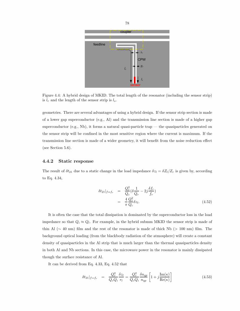
78
feedline
CPW
sensor
coupler
lr
ls
sr
gr
Figure 4.4: A hybrid design of MKID. The total length of the resonator (including the sensor strip)is lr and the length of the sensor strip is ls.
geometries. There are several advantages of using a hybrid design. If the sensor strip section is made
of a lower gap superconductor (e.g., Al) and the transmission line section is made of a higher gap
superconductor (e.g., Nb), it forms a natural quasi-particle trap — the quasiparticles generated on
the sensor strip will be confined in the most sensitive region where the current is maximum. If the
transmission line section is made of a wider geometry, it will benefit from the noise reduction effect
(see Section 5.6).
4.4.2 Static response
The result of δt21 due to a static change in the load impedance δzl = δZl/Zr is given by, according
to Eq. 4.34,
δt21|f=fr =Q2
r
Qc(δ
1
Qr− 2j
δfr
fr)
=4
π
Q2r
Qcδzl. (4.52)
It is often the case that the total dissipation is dominated by the superconductor loss in the load
impedance so that Qi ≈ Ql. For example, in the hybrid submm MKID the sensor strip is made of
thin Al (∼ 40 nm) film and the rest of the resonator is made of thick Nb (> 100 nm) film. The
background optical loading (from the blackbody radiation of the atmosphere) will create a constant
density of quasiparticles in the Al strip that is much larger than the thermal quasiparticles density
in both Al and Nb sections. In this case, the microwave power in the resonator is mainly dissipated
though the surface resistance of Al.
It can be derived from Eq. 4.33, Eq. 4.52 that
δt21|f=fr =Q2
r
QcQi
δzl
rl=
Q2r
QcQi
δnqp
nqp
[1 + j
Im(κ)
Re(κ)
](4.53)

79
which is maximized under critical coupling Qc = Qi
δt21|f=fr , Qc=Qi =1
4
δnqp
nqp
[1 + j
Im(κ)
Re(κ)
]. (4.54)
We can also derive the following formulas
Q−1i = Q−1
l =4Rl
πZr= α∗|γ|Re(κ)nqp
2lslr
(4.55)
δfr
fr= − 2Xl
πZr= −α
2
∗|γ|Im(κ)δnqp
2lslr
(4.56)
where ls is the length of the sensor strip and lr ≈ λ/4 is the total length of the quarter-wave resonator
(including ls, see Fig. 4.4).
4.4.3 Power dissipation in the sensor strip
Before moving onto a discussion of the dynamic response, we first calculate the power dissipation
Pl in the load impedance Zl (sensor strip).
From a signal flow analysis illustrated in Fig. 4.2(c), the current Il flowing through Zl is given
by
Il =V +
A − V −A
Zr=
V +1√Z0Zr
SA1
1 − ΓSAA(1 − Γ) ≈ V +
1√Z0Zr
−2j√
2πQc
1Qr
+ 2j f−fr
fr
. (4.57)
The power dissipated by Zl is given by
Pl =1
2|I2
l |Rl = P+1
2Q2
r
QiQc
1 + 4Q2r
∣∣∣f−fr
fr
∣∣∣2 . (4.58)
Right on resonance f = fr and under critical coupling Qc = Qi, the power dissipated in the load
impedance is half of the input power to port-1
Pl =1
2P+
1 =1
2Pµw . (4.59)
4.4.4 Dynamic response
Assuming that the load impedance has a slow time-dependent variation δZL(t), we would like to
find the corresponding response in the output voltage δV −2 (t).
Here we apply a perturbation analysis to the circuit. We first replace the load impedance Zl
with a resister Rl and a inductor Ll in serial connection, and discuss them separately.
Let VR(t), I(t), and R be the unperturbed voltage, current and resistance of the resistor. And

80
V (t)
R
I(t)
I(t) R
+
-
(a)
L
I(t)
V (t)
L(t)dI(t)/dt
+
-
(b)
1 (Z0)
Zr
ZL
V1+
V2-
S21 2 (Z0)
3 (Zr)
A (Zr)
VA+
VA-
S31
S33
SAA
SA3
L
Vs
(c)
Figure 4.5: Equivalent circuit for (a) δR(t) and (b) δL(t) perturbations. The equivalent networkmodel is shown in (c).
let δVR(t), δI(t), and δR(t) be their perturbations. Considering the total voltage, current, and
resistance with and without the perturbations, we can write down the following equations,
[VR(t) + δVR(t)] = [I(t) + δI(t)][R+ δR(t)] (4.60)
VR(t) = I(t)R. (4.61)
Subtracting Eq. 4.61 from Eq. 4.60 and dropping the 2nd-order terms, we get
δVR(t) = I(t)δR(t) + δI(t)R (4.62)
which suggests an effective circuit as shown in Fig. 4.5(a).
Similarly, for the inductance perturbation we have
δVL(t) = L(t)d
dtδI(t) + δL(t)
d
dtI(t) (4.63)
which suggests an effective circuit as shown in Fig. 4.5(b).
Therefore the effect of the perturbation δZl can be taken into account by adding an effective

81
voltage source δVs(t) to the original network model, as illustrated in Fig. 4.5 (c),
δVs(t) = δR(t)I(t) + δL(t)d
dtI(t). (4.64)
Assume that δR(t) and δL(t) are narrow-banded signal with Fourier transforms
δR(t) =
∫ +∆f
−∆f
δR(f)ej2πftdf
δL(t) =
∫ +∆f
−∆f
δL(f)ej2πftdf . (4.65)
Inserting Eq. 4.65 into Eq. 4.64 and using I(t) = Ilej2πft, we find
δVs(f + f) = Il[δR(f) + i2πfδL(f)] = IlδZl(f) (4.66)
where δVs(f + f) is the Fourier transform of δVs(t). δV−2 (t), the voltage response at port 2, is given
by,
δV −2 (f + f) = V +
A (f + f)
√Z0
ZLS2A(f + f)
=δVs(f + f)
1 − ΓSAA
Zr
Zr + Zl
√Z0
ZrS2A. (4.67)
Now we define a time dependent transmission coefficient t21(t) with its Fourier transform t21(f)
δt21(f) =δV −
2 (f + f)
V +1
. (4.68)
When the output microwave signal V −2 is homodyne mixed with V +
1 using a IQ mixer, the dynamic
trajectory in the IQ plane is described t21(t).
From Eq. 4.57, 4.66, and 4.67, we derive
δt21(f) =4Q2
r
πQc
1
1 + 2jQrf−fr
fr
1
1 + 2jQrf+f−fr
fr
δzl(f). (4.69)
When the resonator is driven on resonance f = fr, we find
δt21(f)|f=fr =4Q2
r
πQc
1
1 + 2jQrffr
δzl(f). (4.70)
Eq. 4.70 shows that under small perturbation δzl, the resonator circuit acts as a low-pass filter
with a bandwidth equal to the resonator’s bandwidth fr/2Q. One can also verify that by setting
f = 0, Eq. 4.70 gives the same static response as derived in Eq. 4.52.

82
In the case that Qi is set by the superconductor loss in the sensor strip, we find
δt21(f)|f=fr =Q2
r
QcQi
δzl(f)
rl
1
1 + 2jQrffr
. (4.71)
We further assume that at any time the instant load impedance ZL(t) depends only on the QP
density nqp(t) at that time. With this assumption, Eq. 4.71 leads to
δt21(f)|f=fr =Q2
r
QcQi
δnqp(f)
nqp
[1 + j
Im(κ)
Re(κ)
]1
1 + 2jQrffr
(4.72)
which is maximized at critical coupling Qc = Qi
δt21(f)|f=fr , Qc=Qi =1
4
δnqp(f)
nqp
[1 + j
Im(κ)
Re(κ)
]1
1 + 2jQrffr
. (4.73)
It’s easy to see that Eq. 4.71, 4.72 and 4.73 are the counterparts of Eq. 4.52, Eq. 4.53, and Eq. 4.54,
respectively.

83
Chapter 5
Excess noise in superconductingmicrowave resonators
5.1 A historical overview of the noise study
The fundamental noise limit for MKIDs is set by the quasiparticle generation-recombination (g-r)
noise (see Section 6.1.1), which decreases exponentially to zero and makes the detector extremely
sensitive as the temperature goes to zero. Unfortunately and unexpectedly, a significant amount
of excess noise was observed in these resonators, which prevents the detectors from achieving the
ultimate sensitivity imposed by the g-r noise. The discovery of this excess noise and a discussion
of its influence on detector NEP dates back to 2003[14]. There we have shown, from the noise
measurement of a 200 nm thick Al on sapphire MKID, that the NEP limited by the excess noise
is two orders of magnitude higher than that limited by the g-r noise, and one order of magnitude
higher than that limited by the HEMT amplifier (due to the coupling limited Q). The origin of this
excess noise remained largely unknown at that time.
Since then, systematic studies of the excess noise have been carried out both theoretically and
experimentally. Early studies were focused on exploring the noise properties and are described in
detail in Mazin’s thesis[15]. Several interesting properties of the excess noise have been observed in
this early work, although some of the discussions and conclusions remained more qualitative than
quantitative. We found that the noise is dominantly a phase noise (or a frequency noise, equivalent
to a jitter in the resonator’s resonance frequency); we observed that the excess noise has a strong
dependence on the microwave readout power. An important discovery was that the Al devices made
on sapphire substrate gave significant lower noise than those made on the Si substrate. Although
in 2003[14] we suggested that the excess noise is too large to be explained by the quasiparticle
fluctuations in the superconductor, the apparent substrate dependence of the noise gave stronger
evidence that the noise is not related to superconductor.
Meanwhile, we began to search for the candidates of the noise source from the literature of low

84
temperature physics. We noticed that excess telegraph noise was reported from the single electron
transistor (SET) community. In one experiment, they were able to constrain the noise source as
being in the substrate by looking at the correlation of the charge fluctuation signals from the two
SETs placed close to each other on the same substrate[58]. Fluctuations of similar origins were also
found in tunnel junctions and were reported from the quantum computing community. By spring
2005, Peter Day, a JPL member of our MKID group, had described in a proposal the idea that the
noise might be generated by two-level tunneling systems in amorphous dielectrics. Our affection to
this possibility was substantially increased by the results of Martinis et al. [59], who found that
the decoherence of their Josephson qubits could be explained by the dielectric loss caused by the
two-level systems (TLS) in the tunnel barrier. TLS are tunneling states in amorphous solids, which
have a broad distribution of energy splitting and can be thermally activated at low temperatures,
causing anomalous properties (thermal, acoustic and dielectric) and noise. It turns out that TLS
were studied as early as in 1960s and a quite established TLS model already existed since the early
1970s[60, 61]. One of the results from Martinis et al. that caught our attention was that the TLS-
induced dielectric loss has a strong saturation effect, a behavior perhaps related to the observed
power dependence of excess noise in our resonators. Since then, TLS has become a strong candidate
for the noise source of our resonators.
The devices tested in the early days were mostly made of Al. In these measurements, the
resonator’s frequency shift and internal loss are dominated by the conductivity of the superconductor.
It was first proposed by Kumar[62, 63] to use Nb resonators to study the low temperature anomalous
frequency shift predicted by the TLS theory, and the temperature dependence of excess noise. For
this purpose, a Nb on Si CPW resonator was fabricated and tested. From this device, we got two
interesting results. First, the noise was seen to decrease dramatically with temperature. Although
we do not know what mechanism causes this phenomenon, this is a strong evidence that the excess
noise is not from the superconductor, because Nb has Tc = 9.2 K and at T < 1 K the contribution
from the conductivity is negligible. Second, the noise level measured from these resonators were as
low as that from the Al on sapphire resonators, contradicting our general experience of higher noise
on Si substrate than sapphire substrate. From this experiment, we began to suspect that the TLS
noise source might be related to the surface or interface, instead of to the bulk substrate, which was
proved to be true in a later experiment.
I started to study the excess noise in 2004, following the early work of Mazin’s thesis. In summary,
progress in three major areas has been made in my thesis. First, the properties of the excess noise,
including power, temperature, material, and geometry dependence, have been quantified; Second,
the TLS, responsible for both the low temperature anomalous frequency shift and the excess noise,
are confirmed to have a surface distribution, while a bulk distribution in substrate has been ruled
out. Three, a semi-empirical noise model has been developed to explain the power and geometry

85
dependence of the noise, which is useful to predict noise for a specified resonator geometry.
The organization of this chapter follows the historical path of the noise study. Following a brief
introduction to the noise measurement setup and the data analysis in Section 5.2, we present the
observed general properties of the excess noise in Section 5.3, including its property of being pure
frequency (phase) noise, the power dependence, temperature dependence, material dependence, and
geometry dependence. These properties give strong evidence that the excess noise is not coming
from the superconductor but from the two level-systems in the dielectric materials in the resonator.
For this reason, we give a review of the standard TLS theory in the first half of Section 5.4. The
established TLS theory may be readily applied to explain the power and temperature dependence
of the resonator’s frequency shift and dissipation, but not the noise. We dedicate the second half
of Section 5.4 to the discussion of the noise model. Because we still do not have a complete TLS
noise model yet, in this section we do not go any further than giving some qualitative and semi-
quantitative discussions. Nevertheless, based on the TLS theory and experimental observations of
the excess noise, we propose a semi-empirical model that is practically useful to predict noise in
the resonators. Guided by the TLS theory, several interesting experiments are designed to test the
TLS hypothesis, which is discussed in Section 5.5. In the first two experiments, TLS are artificially
added into the resonator through a deposited layer of amorphous dielectric material. The behavior
of the resonators loaded with TLS is found to be in good agreement with the TLS theory and
the observed increase of frequency noise in these resonators demonstrates that TLS are able to
act as noise source. The next two experiments, which explore the geometrical scaling of the TLS-
induced frequency shift and noise, are the two critical experiments of this chapter. They give direct
experimental evidence that the TLS are distributed on the surface of the resonator but not in the
bulk substrate. Moreover, the measured geometrical scaling of frequency noise can be satisfactorily
explained by the semi-empirical model introduced in Section 5.4.6. With the knowledge about TLS
and excess noise, we discuss a number of methods that can potentially reduce the excess noise in
Section 5.6, which concludes this chapter.
5.2 Noise measurement and data analysis
The homodyne system used for resonator readout and for noise measurement is illustrated in Fig. 5.1.
A microwave synthesizer generates a microwave signal at frequency f which is used to excite a
resonator. The transmitted signal is amplified with a cryogenic high electron mobility transistor
(HEMT) amplifier mounted at 4 K stage and a room-temperature amplifier, and is then compared
to the original signal using an IQ mixer. The output voltages I and Q of the IQ mixer are proportional
to the in-phase and quadrature amplitudes of the transmitted signal. As f is varied, the output
ξ = [I,Q]T (the superscript T represents the transpose) traces out a resonance circle (Fig. 5.2(a)).
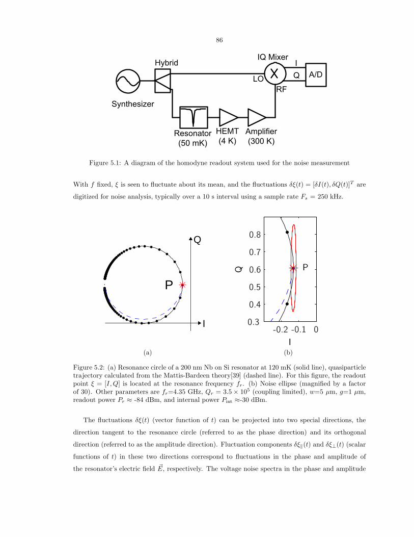
86
Resonator
(50 mK)
HEMT
(4 K)
HybridIQ Mixer
Synthesizer
I
QLO
RF
Amplifier
(300 K)
A/D
Figure 5.1: A diagram of the homodyne readout system used for the noise measurement
With f fixed, ξ is seen to fluctuate about its mean, and the fluctuations δξ(t) = [δI(t), δQ(t)]T are
digitized for noise analysis, typically over a 10 s interval using a sample rate Fs = 250 kHz.
I
Q
P
(a)
I
Q P
-0.2 -0.1 00.3
0.4
0.5
0.6
0.7
0.8
(b)
Figure 5.2: (a) Resonance circle of a 200 nm Nb on Si resonator at 120 mK (solid line), quasiparticletrajectory calculated from the Mattis-Bardeen theory[39] (dashed line). For this figure, the readoutpoint ξ = [I,Q] is located at the resonance frequency fr. (b) Noise ellipse (magnified by a factorof 30). Other parameters are fr=4.35 GHz, Qr = 3.5 × 10⁵ (coupling limited), w=5 µm, g=1 µm,readout power Pr ≈ -84 dBm, and internal power Pint ≈-30 dBm.
The fluctuations δξ(t) (vector function of t) can be projected into two special directions, the
direction tangent to the resonance circle (referred to as the phase direction) and its orthogonal
direction (referred to as the amplitude direction). Fluctuation components δξ‖(t) and δξ⊥(t) (scalar
functions of t) in these two directions correspond to fluctuations in the phase and amplitude of
the resonator’s electric field ~E, respectively. The voltage noise spectra in the phase and amplitude

87
direction can be calculated from
〈δξ‖(ν)δξ∗‖(ν′)〉 = S‖(ν)δ(ν − ν′)
〈δξ⊥(ν)δξ∗⊥(ν′)〉 = S⊥(ν)δ(ν − ν′) (5.1)
where δξ‖(ν) and δξ⊥(ν) are the Fourier transform of the time domain fluctuations δξ‖(t) and δξ⊥(t),
respectively.
The noise data δξ(t) can also be quantified by studying the spectral-domain noise covariance
matrix S(ν), defined by
〈δξ(ν)δξ†(ν′)〉 = S(ν)δ(ν − ν′), S(ν) =
SII(ν) SIQ(ν)
S∗IQ(ν) SQQ(ν)
, (5.2)
where δξ(ν) is the Fourier transform of the time-domain data, the dagger represents the Hermitian
conjugate, SII(ν) and SQQ(ν) are the auto-power spectra, and SIQ(ν) is the cross-power spectrum.
The matrix S(ν) is Hermitian and may be diagonalized using a unitary transformation; however,
we find that the imaginary part of SIQ is negligible and that an ordinary rotation applied to the
real part Re S(ν) gives almost identical results. We calculate the eigenvectors and eigenvalues of
S(ν) at every frequency ν:
OT (ν)ReS(ν)O(ν) =
Saa(ν) 0
0 Sbb(ν)
, (5.3)
where O(ν) = [va(ν), vb(ν)] is an orthogonal rotation matrix. We use Saa(ν) and va(ν) to denote
the larger eigenvalue and its eigenvector.
The total noise power in δξ(t) can be quantified and clearly visualized by plotting a noise ellipse,
defined by
δξTC−1δξ = 1 (5.4)
where
C =
∫ ν2
ν1
ReS(ν)dν (5.5)
is the covariance matrix for δI and δQ filtered for the corresponding bandpass.
The noise in the phase direction can also be described in terms of the phase noise Sθ(ν) and the
(fractional) frequency noise Sδfr (ν)/f2r , because the voltage fluctuations in the phase direction δξ‖
can be viewed as being caused by either fluctuations in the phase angle, δθ (with reference to the
center of the resonance circle) or jitters in the resonator’s resonance frequency, δfr. The voltage
noise S‖(ν), phase noise Sθ(ν) and the frequency noise Sδfr (ν)/f2r are related to each other by the

88
following relationships:
Sδθ(ν) =S‖(ν)
r2, (δθ =
δξ‖r
) (5.6)
Sδfr (ν)/f2r =
Sδθ(ν)
16Q2, (δfr
fr=
δθ
4Q) (5.7)
where r is the radius of the resonance circle. They will be used to compare the excess noise in future
discussions.
In practice, the calculation of the noise spectra (e.g., SII(ν) and SQQ(ν)) can be accomplished
efficiently using the Matlab function “pwelch”[54]. We use “pwelch” to calculate the power spectrum
in three different frequency resolutions for three noise frequency ranges. The noise spectra shown
in this chapter usually are plotted with 1 Hz resolution for 1 Hz ≤ ν < 50 Hz, 10 Hz resolution for
1 Hz ≤ ν < 1 kHz, and 100 Hz resolution for 1 kHz ≤ ν < 125 kHz (Fs/2). Unless noted, the noise
spectra are calculated as double-sided spectra with S(ν) = S(−ν) and only the positive frequencies
are plotted.
5.3 General properties of the excess noise
5.3.1 Pure phase (frequency) noise
Frequency (Hz)
Nois
eP
SD
(dB
c/H
z)
Rota
tion
angle
(deg
)
100 101 102 103 104 10560
90
120
150
-100
-90
-80
-70
-60
-50
-40
Figure 5.3: Noise spectra in the phase (Saa(ν), solid line) and amplitude (Sbb(ν), dashed line)directions, and the rotation angle (φ(ν), dotted line). The noise data are from the same Nb/Siresonator under the same condition as in Fig. 5.2.
A typical pair of spectra Saa(ν) and Sbb(ν) are shown in Fig. 5.3, along with the rotation angle
φ(ν), defined as the angle between va(ν) and the I axis. Three remarkable features are found for

89
all noise data. First, φ(ν) is independent of ν within the resonator bandwidth (the r.m.s. scatter
is σφ ≤ 0.4 per 10 Hz frequency bin from 1 Hz to 5 kHz in Fig. 5.3), which means that only two
special directions, va and vb, diagonalize S(ν). Second, va is always tangent to the IQ resonance
circle while vb is always normal to the circle, even when f is detuned from fr. Because Saa(ν)
and Sbb(ν) are the noise spectra projected into these two constant directions according to Eq. 5.3,
they are equal to the voltage noise spectra calculated from Fourier transform of the projected time
domain noise data δξ‖(t) and δξ⊥(t),
Saa(ν) = S‖(ν)
Sbb(ν) = S⊥(ν). (5.8)
Third, Saa(ν) is well above Sbb(ν) (see Fig. 5.3). When we plot the noise ellipse according to Eq. 5.4
and 5.5 using a integration bandpass ν1 = 1 Hz and ν2 = 1 kHz, we find the major axis of the noise
ellipse is always in the phase direction, and the ratio of the two axes is always very large (8 for the
noise ellipse shown in Fig. 5.2(b)).
Fig. 5.3 also shows that the amplitude noise spectrum is flat except for a 1/ν knee at low frequency
contributed by the electronics. The amplitude noise is independent of whether the synthesizer is
tuned on or off the resonance, and is consistent with the noise temperature of the HEMT amplifier.
The phase noise spectrum has a 1/ν slope below 10 Hz, typically a ν−1/2 slope above 10 Hz, and
a roll-off at the resonator bandwidth fr/2Qr (as is the case in Fig. 5.3) or at the intrinsic noise
bandwidth ∆νn, whichever comes first. The phase noise is well above the HEMT noise, usually
by two or three orders of magnitude (in rad2/Hz) at low frequencies. It is well in excess of the
synthesizer phase noise contribution or the readout system noise.
Quasi-particle fluctuations in the superconductor, perhaps produced by temperature variations
or the absorption of high frequency radiation, can be securely ruled out as the source of the measured
noise by considering the direction in the IQ plane that would correspond to a change in quasi-particle
density δnqp. According to the discussion in Section 2.4, both the real and inductive parts of the
complex conductivity σ respond linearly to δnqp, δσ = δσ1−iδσ2 = κ|σ|δnqp, resulting in a trajectory
that is always at a nonzero angle ψ = tan−1(δσ1/δσ2) to the resonance circle, as indicated by the
dashed lines in Fig. 5.2(a) and (b). Mattis-Bardeen calculations yield ψ = tan−1[Re(κ)/Im(κ)] > 7
for Nb below 1 K, so quasi-particle fluctuations are strongly excluded, since ψ >> σφ. Furthermore,
ψ is measured experimentally by examining the response to X-ray, optical/UV, or submillimeter
photons, and is typically ψ ≈ 15 ([24, 50], and see Section 5.6.3).

90
100 101
102 103104 105
10−10
10− 9
10− 8
10− 7
10− 6
-99 dBm -95 dBm -91 dBm -87 dBm
Frequency (Hz)
Vo
lta
ge
no
ise
PS
D (
V /
Hz)
2
(a)
Fra
ctio
na
lfr
eq
uency
no
ise
(1/H
z)
Frequency (Hz)
Pha
se
no
ise
(ra
d2/H
z)
100 101 102 103 104 105
10−9
10−8
10−7
10−6
10−5
10−21
10−20
10−19
10−18
10−17
10−16
-99 dBm -95 dBm -91 dBm -87 dBm
(b)
Figure 5.4: Excess noise in the phase direction under different readout powers Pµw. (a) Voltagenoise spectrum S‖(ν). (b) Phase noise spectrum Sδθ(ν) (left axis) and fractional frequency noisespectrum Sδfr (ν)/f2
r (right axis). The readout powers of the 4 curves are Pµw =-87 dBm, -91 dBm,-95 dBm, -99 dBm from top to bottom in (a) and from bottom to top in (b). The data is measuredfrom a 200 nm thick Al on sapphire resonator.
5.3.2 Power dependence
The excess noise has a dependence on the microwave readout power Pµw. Fig. 5.4 compares the
measured noise spectra of a resonator under four different readout powers in steps of 4 dBm. We
found the voltage noise increases with the readout power, as shown in Fig. 5.4(a). A 2 dB separation
is found between the two adjacent noise spectra, suggesting
S‖(ν) ∝ P12
µw. (5.9)
The excess noise, when converted to phase noise or frequency noise, decreases with readout power.
The same separation of 2 dB but with a reversed order (top curve with the lowest Pµw) is seen in
Fig. 5.4(b), which suggests:
Sδθ(ν) ∝ P− 1
2µw , Sδfr (ν)/f2
r ∝ P− 1
2µw . (5.10)
Eq. 5.9 and Eq. 5.10 are consistent because the radius of the resonance loop r scales as r ∝ P12
µw .
To compare the excess noise among resonators with different fr and Qr, we plot the frequency
noise Sδfr (ν)/f2r as a function of the microwave power inside the resonator (the internal power). It
can be shown that the internal power Pint is related to the readout power Pµw by
Pint =2
π
Q2r
QcPµw (5.11)
for a quarter-wave resonator.
The frequency noise vs. internal power for resonators with different fr and Qr on the same

91
Internal Power (dBm)
S(1kHz)
/f
(1
/Hz)
-54 -52 -50 -48 -46 -44 -42 -40 -38 -36
10-19
10 -18
δf r
r
2
Figure 5.5: Frequency noise at 1 kHz Sδfr (1 kHz)/f2r vs. internal power Pint falls on to straight lines
of slope -1/2 in the log-log plot indicating a power law dependance: Sδfr/fr∝ P
−1/2int . Data points
marked with“+”,“”, and “*” indicate the on-resonance (f = fr) noise of three different resonators(with different fr and Qr on the same chip) under four different Pµw . Data points marked with“” indicate the noise of resonator 1 (marked with “*”) measured at half-bandwidth away from theresonance frequency (f = fr ± fr/2Qr) under the same four Pµw. The data is measured from a 200nm thick Al on sapphire device.
substrate are compared in Fig. 5.5. The data points, from three different resonators, four different
readout powers, driven on-resonance and detuned, fall nicely onto a straight line of slope -1/2 in the
log-log plot, suggesting that the frequency noise depends on the internal power Pint of the resonator
by a power law
Sδfr (ν)/f2r ∝ P
− 12
int . (5.12)
The power law index -1/2 in Eq. 5.12 is suggestive. For comparison, amplifier phase noise is a
multiplicative effect that would give a constant noise level independent of Pint, while the amplifier
noise temperature is an additive effect that would produce a 1/Pint dependence.
5.3.3 Metal-substrate dependence
The excess noise also depends on the materials used for the resonator. In Fig. 5.6, we plot the
frequency noise spectrum at 1 KHz Sδfr (1 kHz)/f2r against internal power Pint for five resonators
made of different metal-substrate combinations (all substrates used are crystalline substrates). In
addition to the power dependence Sδfr (ν)/f2r ∝ P
−1/2int , we find that the noise levels are material
dependent. In general, sapphire substrates give lower phase noise than Si or Ge, roughly by an
order of magnitude in the noise power. However the Nb/Si resonator showed low noise comparable
with Al/sapphire resonator, suggesting that the etching or interface chemistry, which is different for
Nb and Al, may play a role. Two Al/Si resonators with very different Al thicknesses and kinetic

92
inductance fractions[64] fall onto the dashed equal-noise scaling line, strongly suggesting that the
superconductor is not responsible for the phase noise.
320 nm Al on Si40 nm Al on Si200 nm Nb on Si200 nm Al on Sapphire200 nm Al on Ge
Internal Power (dBm)
Sδf r
(1kH
z)/
f2 r(1
/Hz)
-60 -55 -50 -45 -40 -35 -30 -25 -20 -1510−20
10 −19
10 −18
10 −17
Figure 5.6: Power and material dependence of the frequency noise at ν = 1 kHz. All the resonatorsshown in this plot have w=3 µm, g=2 µm and are measured around 120 mK. The spectra used inthis plot are single-sided (ν > 0).
As will be discussed in great detail later in this chapter, the TLS on the surface of the resonator,
either metal surface or the exposed substrate surface, are responsible for the excess noise. Therefore,
the metal-substrate dependence of the excess noise shown in Fig. 5.6 turns out to have nothing to
do with the bulk properties of the superconductor or the substrate. Instead, it’s their surface or
interface properties that make a difference. For example, the metal Al, Nb and crystalline Si, Ge can
all form a native oxide layer on the surface, which can be the host material of the TLS. The defects,
impurities and chemical residues introduced during etching and other processes of the fabrication
may be another source of TLS.
5.3.4 Temperature dependence
The temperature dependence of the excess frequency noise is best demonstrated by the experiment
in which the noise of a Nb on Si resonator is measured at temperatures below 1 K. Because Nb
has a transition temperature Tc = 9.2 K, the noise contribution from superconductor are frozen at
T < 1 K. Any temperature dependence of noise has to be from other low energy excitations — TLS
in the resonator.
Fig. 5.7 shows the measured phase and amplitude noise spectra under readout power Pµw =
−85 dBm at several temperatures between 120 mK and 1200 mK. While the amplitude noise (S⊥(ν),
in green) remains almost unchanged, the phase noise (S‖(ν), in blue) decreases steeply with temper-
ature. As mentioned earlier, the amplitude noise spectrum S⊥(ν) is consistent with the noise floor

93
100
101
102
103
104
105
10−4
10−2
100
102
Vol
tage
noi
se P
SD
[AD
U2 /H
z]
Frequency [Hz]
S||
S⊥S
|| − S⊥
Figure 5.7: Phase noise (S‖(ν), blue curves) and amplitude noise (S⊥(ν), green curves) spectrameasured at T=120, 240, 400, 520, 640, 760, 880, 1000, 1120 mK (from top to bottom). The truephase noise can be calculated by subtracting the amplitude noise from the phase noise, which isplotted as the red curves. The voltage unit used here is the unit of our AD card with 1 V =32767 ADU. The data is measured from a 200 nm Nb on Si resonator under a fixed readout powerPµw = −85 dBm.
of the readout electronics (mainly limited by the noise temperature of our HEMT). Therefore, we
calculate the “true” phase noise by subtracting the measured S⊥(ν) from S‖(ν) and the results are
plotted in red curves in Fig. 5.7.
To better quantify the temperature and power dependence of the frequency noise, we retrieve
the noise values at 1 kHz from the phase noise spectrum (red curve) at each readout power and each
temperature. The 1 kHz frequency noise Sδfr (1 kHz)/f2r is plotted as a function of Pµw and T in
Fig. 5.8. The even spacing (∼ 2 dB) between any two adjacent noise curves indicates the P−1/2int
dependence of frequency noise as expected. At a fixed Pµw, we find the frequency noise roughly
falls onto a power-law relationship and at intermediate temperatures 300 mK < T < 900 mK the
temperature dependence is close to
Sδfr (1 kHz)/f2r ∝ T−2 (5.13)
as indicated by the parallel solid lines in Fig. 5.8. This scaling is consistent with the T−1.73 scaling
found by Kumar[63], where he was fitting for a broader range of temperatures.
In addition to the noise, the resonance frequency fr and quality factor Qr also show strong
temperature dependence, which are shown in Fig. 5.9. Later in this chapter we will see plenty
examples of similar fr(T ) and Qr(T ) curves and show that they can be well explained by the TLS
theory.

94
102
103
10−22
10−21
10−20
10−19
10−18
T [mK]
Sδ
f r(1 k
Hz)
/f r2 [1/H
z] T−2
Figure 5.8: Frequency noise at ν = 1 kHz as a function of temperature under several readout powers.The readout powers Pµw are from -105 dBm to -73 dBm in step of 4 dBm from top to bottom. Thesolid lines indicate T−2 temperature dependence. The data is measured from a 200 nm Nb on Siresonator.
In summary, the measured temperature dependence of resonance frequency, quality factor, and
frequency noise strongly suggest to us that TLS in the dielectric materials are responsible for the
noise.
5.3.5 Geometry dependence
The geometry dependence of the frequency noise was carefully studied with a Nb on sapphire
geometry-test device, which contains CPW resonators with five different center strip widths (sr
=3 µm, 5 µm, 10 µm, 20 µm, and 50 µm) and with the ratio between the center strip width and the
gap width fixed to 3:2. Here we only present the conclusions, while leaving the detailed data and
analysis to Section 5.5.2.2, after the introduction of TLS theory and a semi-empirical noise model.
Fig. 5.10 shows the measured frequency noise (before and after the correction for coupler’s noise
contribution) at ν = 2 kHz as a function of center strip width sr under the same internal power
Pint = −25 dBm. We find that the frequency noise has a geometrical scaling
Sδfr (ν)/f2r ∝ 1/s1.6
r . (5.14)
The noise data as well as the temperature-dependent fr(T ) and Qr(T ) data measured from this
geometry-test device will be discussed in great detail in Section 5.5.2.2. As we will show there, these
data not only confirm the TLS hypothesis but further point to a surface distribution of TLS and
rule out a uniform distribution of TLS in the bulk substrate.

95
0 200 400 600 800 1000 12004.3472
4.3473
4.3473
4.3473
4.3473
4.3473
T [mK]
f r [GH
z]
200 400 600 800 1000 12001.5
2
2.5
3
3.5
4
4.5x 10
5
T [mK]
Q
Figure 5.9: Resonance frequency (a) and quality factor (b) as a function of temperature under severalreadout powers. The readout powers Pµw are from -105 dBm to -73 dBm in steps of 4 dBm frombottom to top in both plots. The data is measured from a 200 nm Nb on Si resonator.
5.4 Two-level system model
In this section, we first give a review of the standard two-level system (TLS) theory. Then we present
a semi-empirical TLS noise model.
5.4.1 Tunneling states
Experiments show that amorphous solids exhibit very different thermal, acoustic, and dielectric
properties from crystalline solids at low temperatures. In 1972, the standard two-level system
model was independently introduced by Phillips[60] and Anderson[61], which satisfactorily explains
the experimental results. This model assumes that a broad spectrum of tunneling states exist in
amorphous solids. Although the microscopic nature of the TLS is still unknown, it is often thought
that in a disordered solid, one or a group of atoms can tunnel between two sites. These tunneling
states have elastic and electric dipole moments that can couple to the elastic and electric fields.
Such a tunneling two-level system can be quantum mechanically treated as a particle in a double-
well potential, as illustrated in Fig. 5.11.
In the local basis (φ1 and φ2), the system Hamitonian can be written as
H =1
2
−∆ ∆0
∆0 ∆
, (5.15)
where ∆ is called the asymmetric energy which equals the energy difference between the right well
and the left well. ∆0 is the tunneling matrix element.
In the standard TLS theory, a uniform distribution in ∆ and a log uniform distribution in ∆0 is

96
3 5 10 2010
−20
10−19
10−18
s [µm]
Sδf
r (2
kHz)
/f2 r [1/
Hz]
uncorrectedcorrected
s−1.58
Figure 5.10: The frequency noise Sδf (2 kHz)/f2r at Pint = −25 dBm measured from the geometry-test
device is plotted as a function of the center strip width sr. Values before and after the correction forthe coupler’s noise contribution are indicated by the squares and stars, respectively. The correctedvalues of Sδf (2 kHz)/f2
r scale as s−1.58r , as indicated by the dashed line. Refer to Section 5.5.2.2 for
details on the device, noise data, and analysis.
assumed
P (∆,∆0)d∆d∆0 =P0
∆0d∆d∆0 (5.16)
where P0 is the two-level density of state found to be on the order of 1044/J·m3.
The Hamiltonian in Eq. 5.15 can be diagonalized to give the eigenenergies ±ε/2 where
ε =√
∆2 + ∆20. (5.17)
The true eigenstates ψ1 and ψ2 can be written in terms of φ1 and φ2 as
ψ1 = φ1 cos θ + φ2 sin θ (5.18)
ψ2 = φ1 sin θ − φ2 cos θ (5.19)
where
tan 2θ =∆0
∆. (5.20)
In the diagonal representation (ψ1, ψ2) the Hamiltonian is in the form of a standard TLS,
H0 =1
2εσz (5.21)
where
σx =
0 1
1 0
, σy =
0 −ii 0
σz =
1 0
0 −1
(5.22)

97
Figure 5.11: A illustration of a particle in a double-well potential
are the Pauli matrices.
5.4.2 Two-level dynamics and the Bloch equations
TLS can interact with an external electric field ~E and strain field e. It can be shown that the
dominant effect of the external fields on the TLS is through the perturbation in the asymmetry
energy ∆, while changes in the tunnel barrier ∆0 can usually be ignored[65]. In the electric problem,
the interaction Hamiltonian can be written as (in ψ1, ψ2 basis)
Heint =
[∆
εσz +
∆0
εσx
]~d0 · ~E. (5.23)
We recognize
~d′ = 2 ~d0∆
ε(5.24)
as the permanent electric dipole moment and
~d = ~d0∆0
ε(5.25)
as the transition electric dipole moment[66]. Because ∆0 ≤ ε, the maximum transition dipole
moment of a TLS with energy splitting ε is ~d0. Later we will see that the first term in Eq. 5.23 gives
rise to a relaxation response and the second term gives a resonant response to the electric field. In
our problem of TLS in a microwave resonator, Heint gives the coupling between the TLS and the
microwave photons.

98
Similarly, in the acoustic problem, the interaction Hamiltonian can be written as
Haint =
[∆
εσz +
∆0
εσx
]γe (5.26)
where γ is the elastic dipole moment and e is the strain field. In our problem, Haint couples the TLS
to the phonon bath and causes relaxations.
The Hamitonian of TLS in the electric problem
H = H0 +Heint (5.27)
has a formal analogy to that of a spin 1/2 system in a magnetic field
H = −~γ ~B · ~S = −~γ( ~B0 · ~S) − ~γ( ~B′ · ~S) (5.28)
where ~B0 is the static magnetic field, ~B′ is the (oscillating) perturbation field, and ~S = ~σ/2.
Comparing Eq. 5.23 to Eq. 5.28, we identify the following correspondence
− ~γ ~B = (0, 0, ε) and − ~γ ~B′ = (2~d · ~E, 0, ~d′ · ~E). (5.29)
Without relaxation processes, the dynamic equation for a free spin in a magnetic field is simply
d
dt~S(t) = γ~S × ~B (5.30)
where ~S(t) can be either interpreted as the spin operator in Heisenberg picture or as the classical
spin (because the quantum mechanical and classical equation take the same form in this problem).
When the relaxation processes are considered, the evolution of the ensemble average of the spin
operators 〈Si(t)〉 is described by the famous Bloch equations, which were first derived to describe
the nuclear magnetic resonance[67]:
d
dt〈Sx(t)〉 = γ (〈Sy〉Bz − 〈Sz〉By) − 〈Sx〉
T2= 0
d
dt〈Sy(t)〉 = γ (〈Sz〉Bx − 〈Sx〉Bz) −
〈Sy〉T2
= 0
d
dt〈Sz(t)〉 = γ (〈Sx〉By − 〈Sy〉Bx) − 〈Sz〉 − Seq
z [Bz(t)]
T1(5.31)
where T1 and T2 are the longitudinal and transverse relaxation times, respectively, and
Seqz [Bz(t)] =
1
2tanh(
~γBz(t)
2kT) (5.32)

99
is the instantaneous equilibrium value of Sz.
5.4.3 Solution to the Bloch equations
To solve the Bloch equations in Eq. 5.31, we first set up the magnetic field as
~B0 = (0, 0, B0) , ~B′ = 2 ~B1 cosωt =
(B1
x, 0, B1z
)(ejωt + e−jωt). (5.33)
Here we enforce B0 < 0. Next, we linearize the term Seqz [Bz(t)] with its Taylor expansion assuming
B1z ≪ |B0|
Seqz [Bz(t)] = Seq
z (B0) +B′z(t)dS
eqz /dB0. (5.34)
Because the perturbation field in Eq. 5.33 is time harmonic, the steady state solution to Eq. 5.31
can be written as a sum of frequency components at ωm = mω (m is an integer)
⟨~S(t)
⟩=
m=+∞∑
m=−∞
~Sm exp(jωmt). (5.35)
By inserting Eq. 5.35 and Eq. 5.33 into Eq. 5.31 and equating the coefficient in front of exp(jωmt)
on the left- and right-hand sides of Eq. 5.31, one will obtain a set of coupled linear equations for
Sm. It can be shown that only equations for m = −1, 0,+1 are important.
The solutions to these equations are given, for example, by Hunklinger[68]. Note that he used
Sm to represent the coefficient for the frequency component e−jωmt, while here we use it for the
frequency component ejωmt. Therefore, a substitution of −ω for ω will convert his results to ours.
The magnetic susceptibilities χi(ω) are defined by
S1x = χx(ω)~γB1
x
S1z = χz(ω)~γB1
z (5.36)
and are derived to be
χx(ω) = −S0z
2~
[1
ω0 − ω + jT−12
+1
ω0 + ω − jT−12
](5.37)
χz(ω) =dSeq
z
d(~γB0)
1 − jωT1
1 + ω2T 21
(5.38)
where ω0 = −γB0 and
S0z =
1 + (ω0 − ω)2T 22
1 + (γB1x)2T1T2 + (ω0 − ω)2T 2
2
Seqz . (5.39)

100
The susceptibilities χx(ω) and χz(ω) are of two different origins: χx(ω) describes the resonant
response of the spins to the ac magnetic field, while χz(ω) has the typical form of a relaxation
process. Furthermore, the first term in Eq. 5.37 is the response to the rotating wave and the second
term is to the counter rotating wave.
The results for spins in magnetic field can be easily converted to the results for our problem —
TLS in an electric field coupled to a phonon bath—by applying the correspondence in Eq. 5.29. For
TLS in an electric field, we define an electric susceptibility tensor for the resonance process
χ res (ω)
and a susceptibility tensor for the relaxation process
χ rel (ω)
⟨~d⟩
=
χ res (ω) · ~E (5.40)⟨~d′⟩
=
χ rel (ω) · ~E. (5.41)
It can be shown that
χ res (ω) = −σ0z
~
[1
ωε − ω + jT−12
+1
ωε + ω − jT−12
]~d~d (5.42)
χ rel (ω) = −dσeqz (ε)
dε
1 − jωT1
1 + ω2T 21
~d′ ~d′ (5.43)
where
σeqz (ε) = − tanh(
ε
2kT) (5.44)
σ0z =
1 + (ωε − ω)2T 22
1 + Ω2T1T2 + (ωε − ω)2T 22
σeqz (ε). (5.45)
Here ωε = ε/~ and Ω = 2~d · ~E/~ is the Rabi frequency.
5.4.4 Relaxation time T1 and T2
In absence of an external field, the Bloch equation for 〈σz〉 becomes
d
dt〈σz〉 = −〈σz〉 − σeq
z
T1. (5.46)
Because 〈σz〉 = p1−p2 is equal to the population difference between the upper and lower states, T−11
relaxation rate is the rate at which a non-equilibrium population relaxes to its equilibrium value,
through the interaction with the phonon bath. Both phonon emission and absorption contribute
to this relaxation process. When the two-level population is in thermal equilibrium, the phonon
emission and absorption processes are balanced and the population stays unchanged. If the two-
level population is out of equilibrium, one phonon process will dominate over the other, always

101
pulling the system back to its equilibrium. It can be shown that T1 is given by [66]
1
T1=
(∆0
ε
)21
T1,min(5.47)
1
T1,min=
[γ2L
v5L
+γ2T
v5T
]ε3
2πρ~4coth(
ε
2kT) (5.48)
where γL and γT are the longitudinal and transverse deformation potential, respectively, vL and vT
are the longitudinal and transverse sound velocity, respectively, and ρ is the mass density. T1,min is
the minimum T1 time for a TLS with splitting energy ε.
The transverse relaxation time T2 is also called the dephasing time. In absence of the external
field, the transverse spin operators in Heisenberg picture will be precessing about the z axis and the
σ+ = σx + jσy operator is given by,
σ+(t) = σ+(0) exp(−j ε~t). (5.49)
If the energy level ε fluctuates with time and the fluctuations δε are not identical for different TLS,
even if an ensemble of TLS starts with the same spin σ+(0) (in phase), they will no longer be in
phase after a period of time. Each spin picks up a random phase θ(t) =∫ t
0δε(τ)dτ and the ensemble
average value of 〈σ+〉 (or the transverse spin components 〈σx〉 and 〈σy〉) will decay to zero in a rate
that is dictated by 1/T2, because usually⟨e−jθ(t)
⟩has a behavior of exponential decay1:
⟨e−j
∫ t0
δε(τ)dτ⟩∼ e−t/T2 (5.50)
For TLS in an amorphous material, the energy level fluctuation δε(t) is described by a “diffusion”
process, referred to as spectral diffusion. As shown in Fig. 5.12, the energy levels gradually spread
out and in the long time limit (t≫ T ∗1 with T ∗
1 being the average T1 time), δε reaches a stationary
distribution with a width of ∆ε. And T2 is inversely proportional to ∆ε. Roughly speaking, T2 is
the time for which the spread in the random phase θ is of the order π/2 and can be estimated by
T−12 =
2
π
∆ε
~. (5.51)
The major contribution to the energy level fluctuations δε is through the TLS-TLS interaction. The
interaction energy between two TLS (i, j) is given by[65]
δεij = c∆i
εi
∆j
εj
γiγj
ρv2r3ij(5.52)
1Depending on the detailed process of δε(t), the decay generally has a more complicated form than a singleexponential and is not always compatible with the single T2-rate description used in the Bloch equations.

102
Figure 5.12: An illustration of spectral diffusion. Figure from [65]
where γi∆/ε and γj∆/ε are the permanent elastic dipole moments of the two TLS, rij is the distance
between the two TLS, and C is a constant of order unity. Physically, Eq. 5.52 describes the process
in which one TLS changes its states and produces a strain field that is felt by another TLS. Replacing
1/r3ij with the volume density of thermally excitable TLS P0kT and averaging over the neighboring
TLS j leads to
∆ε ∼ Cγ2PkT
ρv2
∆
ε(5.53)
and therefore
T−12 ∼ C
2γ2PkT
π~ρv2
∆
ε(5.54)
is expected to have a linear dependence on temperature.
5.4.5 Dielectric properties under weak and strong electric fields
At microwave frequencies (ω ∼ 109 Hz) and at low temperatures (T < 1 K, T1 > 1 µs), ωT1 ≫ 1
and the relaxation contribution given by Eq. 5.43 is much smaller than the resonant contribution
given by Eq. 5.43. Therefore, we will give no further discussion on the relaxation contribution.
For the resonant interaction, the TLS contribution to the (isotropic) dielectric function is given
by
ǫTLS(ω) =
∫∫∫ [e·
χ res (ω) · e] P
∆0d∆d∆0dd = ǫ′TLS(ω) − jǫ′′TLS(ω) (5.55)
where we have averaged over the TLS asymmetry ∆, tunnel splitting ∆0, and dipole orientation d.

103
5.4.5.1 Weak field
If the electric field is weak and the condition Ω2T1T2 ≪ 1 is satisfied, Eq. 5.55 can be worked out
(see Appendix G)
ǫTLS(ω) =
∫ εmax
0
Pd20
3~tanh
(ε
2kBT
)[1
ωε − ω + jT−12
+1
ωε + ω − jT−12
]dε (5.56)
= −2Pd20
3
[Ψ
(1
2− ~ω − j~T−1
2
2jπkBT
)− log
εmax
2πkBT
](5.57)
where Ψ is the complex digamma function and εmax is the maximum energy splitting of TLS.
The TLS contribution to the dielectric loss tangent δ is given by
δTLS =ǫ′′TLS(ω)
ǫ= δ0TLS tanh
(~ω
2kBT
)(5.58)
where the relationship[52] ImΨ(1/2 + jy) = (π/2) tanhπy has been applied, and δ0TLS = πPd20/3ǫ
represents the TLS-induced loss tangent at zero temperature in weak electric field. Here ǫ is the
dielectric constant of the TLS hosting material.
Similarly, the TLS contribution to the real part of the dielectric constant is given by
ǫ′TLS(ω)
ǫ= −2δ0TLS
π
[ReΨ
(1
2− ~ω
2jπkBT
)− log
εmax
2πkBT
](5.59)
where ~T−1/2πkT ≪ 1/2 has been neglected and the sign before ~ω/2jπkT can take either “+” or
“-”, because Ψ(z) = Ψ(z).
Eq. 5.58 for the loss tangent can be alternatively derived by considering the imaginary part of
the integral in Eq. 5.56. The major contribution to this integral is from the resonant absorption
term
Im
[1
ωε − ω + jT−12
]=
T−12
(ωε − ω)2 + (T−12 )2
(5.60)
which is a narrow Lorentzian peak centered at ω with a line width T−12 . Physically it means only
the TLS close to resonance ωε ≈ ω have significant contribution the loss tangent. Neglecting the
1/(ωε +ω+ jT−12 ) term and pulling tanh(ε/2kT ) out of the integral as tanh(~ω/2kT ) will yield the
same result for δTLS in Eq. 5.58.
Eq. 5.58 and Eq. 5.59 are the two important results of TLS theory. The predicted temperature
dependence is illustrated in Fig. 5.13. The loss tangent δTLS (blue curve) is highest (δTLS = δ0TLS)
at low temperatures T . ~ω/2k, and decreases monotonically with T , as 1/T at high temperatures
T ≫ ~ω/2k. ǫ′TLS (red curve) has a non-monotonic behavior: ǫ′TLS increases with T when T < ~ω/2k;
ǫ′TLS decreases when T > ~ω/2k; a maximum in ǫ′TLS occurs around T = ~ω/2k.
The predicted temperature and frequency dependence of δTLS and ǫ′TLS have been tested on all

104
1 2 3 4 5
1.0
0.5
0.0
0.5
1.0 )2
tanh(kT
)2
log()]22
1(Re[
kTjkT !
!
"
##
kT
Figure 5.13: Temperature dependence of δTLS (blue curve) and ǫ′TLS (red curve)
kinds of amorphous solids and are found to be in great agreement with the experiments. Eq. 5.58
and Eq. 5.59 have been used extensively to derive the values of δ0TLS for different materials. We use
them in the experiments described in Section 5.5 to obtain crucial information of the TLS in our
resonators.
5.4.5.2 Strong field
For general and strong electric field, ǫTLS(ω) has to be evaluated from the full integral
ǫTLS(ω) =
∫ εmax
0
Pd20
3tanh
(ε
2kBT
)[1 + (ωε − ω)2T 2
2
1 + Ω2T1T2 + (ωε − ω)2T 2
2
]
×[
1
ωε − ω + jT−12
+1
ωε + ω − jT−12
]dε (5.61)
where
Ω =2d0| ~E|√
3~
∆0
ε(5.62)
is the modified Rabi frequency accounting for the orientation integral (see Appendix G).
For the imaginary part of the integral, the main contribution is still from the 1/(ωε −ω− jT−12 )
term. By dropping the other term 1/(ωε+ω−jT−12 ), the integrand now contains a power-broadened
absorption profile
[1 + (ωε − ω)2T 2
2
1 + Ω2T1T2 + (ωε − ω)2T 2
2
]× Im
[1
ωε − ω + jT−12
]=
−T−12[
T−12
√1 + Ω
2T1T2
]2+ (ωε − ω)2
(5.63)
where the width of the Lorentzian is broadened by a factor of κ =
√1 + Ω
2T1T2. As a result, the

105
TLS loss tangent
δTLS = δ0TLS
tanh(
ε2kBT
)
√1 + Ω
2T1T2
(5.64)
is reduced by a factor of κ from the weak field result.
0.1 1 10 100
1.00
0.50
0.20
0.10
0.05
0.02
cE
Ex
21
1
x!
Figure 5.14: Electric field strength dependence of δTLS
Because Ω ∝ | ~E|, the loss tangent δTLS depends on the electric field strength as
δTLS(| ~E|) =δTLS(| ~E| = 0)√
1 + | ~E/Ec|2(5.65)
where Ec is a critical field for TLS saturation defined as
Ec =
√3~
2d0| ~E|√T1,minT2
. (5.66)
The | ~E| dependence of δTLS is illustrated in Fig. 5.14, where we see that δTLS scales as | ~E|−1 in
a strong electric field | ~E| ≫ Ec.
The real part of the integral in Eq. 5.61 can also be approximately evaluated. Because
Re[1
ωε − ω + jT−12
] ∼ 1
ωε − ω, Re[
1
ωε + ω − jT−12
] ∼ 1
ωε + ω(5.67)
does not converge (yielding logarithmic divergence) when integrated to a large εmax, it means that
the contribution to ǫ′TLS from large detuned TLS is not negligible. In other words, TLS from a
broad range of energy, on-resonance and detuned, all contribute to ǫ′TLS. In addition, we find that
the contributions from the two terms in Eq. 5.67 are comparable and therefore none of them can be

106
neglected. After making a number of mathematical approximations, we derive 2(see Appendix G)
ǫ′TLS(κ) − ǫ′TLS(0)
ǫ= δ0TLS(1 − κ)sech2(
~ω
2kT)~T−1
2
2kT+ δ0TLS tanh(
~ω
2kT)1 − κ2
κ
T−12
2ω(5.68)
where ǫ′TLS(0) is the weak field result given by Eq. 5.59. Usually κ~T−12 ≪ kT and κT−1
2 ≪ ω,
therefore, the power dependence of ǫ′TLS has a very small effect.
5.4.6 A semi-empirical noise model assuming independent surface TLS
fluctuators
We assume that the TLS have a uniform spatial distribution within a volume of TLS-host material
Vh that occupies some portion of the total resonator volume V . Consider a TLS labeled α, located
at a random position ~rα ∈ Vh and with an energy level separation εα = (∆2α + ∆2
0,α). The TLS
transition dipole moment is given by ~dα = dαd0∆0,α/εα, where the dipole orientation unit vector
dα is assumed to be random and isotropically distributed. In the weak–field, linear response limit,
the TLS contribution to the dielectric tensor of the hosting medium is
ǫ TLS (ω,~r) = −∑
α
~d~dδ(~r − ~rα)
[1
εα − ~ω + jΓα+
1
εα + ~ω − jΓα
]σz,α. (5.69)
Eq. 5.69 looks very similar to Eq. 5.42 but the interpretations are quite different. In Eq. 5.42 σ0z is
the ensemble average of σz when the system is in steady-state. Here σz,α is used microscopically to
represent the state of an individual TLS at time t which takes values of −1 for the lower state of the
TLS and +1 for the upper state. We also replaced the dephasing linewidth T−12 , which is an average
effect, with a general linewidth Γ. Averaging over the TLS position, asymmetry, tunnel splitting,
and dipole orientation, and assuming a thermal distribution for the level population, Eq. 5.69 gives
the same result for the TLS contribution to the (isotropic) dielectric function as in Eq. 5.57
ǫTLS(ω) = −2Pd20
3
[Ψ
(1
2− ~ω − jΓ
2jπkBT
)− log
εmax
2πkBT
]. (5.70)
As derived earlier, the real (ǫ′TLS) and imaginary (ǫ′′TLS) parts of ǫTLS yield the well-known results
for the TLS contribution to the dielectric constant Eq. 5.59 and loss tangent Eq. 5.58. When these
TLS are coupled to the resonator, the average effects to the frequency shift and quality factor can
be derived both classically from the cavity perturbation theory given by Pozar[57] and quantum-
2I have derived this formula by myself which hasn’t been tested by any experiment yet.

107
mechanically from the cavity QED theory[69]. The results for weak field are
∆fr
fr= −
∫Vhǫ′TLS| ~E|2 d~r
2∫
Vǫ| ~E|2 d~r
=Fδ0TLS
π
[ReΨ
(1
2− ~ω
2jπkBT
)− log
εmax
2πkBT
](5.71)
∆1
Qr= −
∫Vhǫ′′TLS| ~E|2 d~r∫
Vǫ| ~E|2 d~r
= Fδ0TLS tanh
(~ω
2kT
)(5.72)
where δ0TLS = 3Pd20/2ǫh and
F =
∫Vhǫh ~E(~r)2d~r
∫V ǫ
~E(~r)2d~r=we
h
we. (5.73)
F is a filling factor which accounts for the fact that the TLS host material volume Vh may only
partially fill the resonator volume V , giving a reduced effect on the variation of resonance frequency
and quality factor. According to Eq. 5.73, F is the ratio of the electric energy weh stored in the
TLS-loaded volume to the total electric energy we stored in the entire resonator.
It can be derived from Eq. 5.71 that the TLS-induced temperature variation of frequency shift
is given by
fr(T ) − fr(0)
fr=Fδ0TLS
π
[ReΨ
(1
2− ~ω
2jπkBT
)− log
~ω
2πkBT
]. (5.74)
If the internal loss of the resonator is dominated by the TLS-induced dielectric loss, the internal
quality factor Qi has a temperature dependence given by
1
Qi(T )= Fδ0TLS tanh
(~ω
2kT
). (5.75)
In Section 5.5, Eq. 5.74 and Eq. 5.75 are directly applied to the experimental data of ∆fr(T )/fr
and 1/Qi(T ) measured at T << Tc, to retrieve Fδ0TLS for each resonator.
Now, if the dielectric constant fluctuates on time scales τǫ ≫ 1/ω, according to Eq. 5.71, we
would expect to see resonator frequency fluctuations given by
δfr(t)
fr= −
∫Vhǫ′TLS(~r, t)| ~E|2 d~r2∫
V ǫ| ~E|2 d~r. (5.76)
From Eq. 5.69, we see that ǫ′TLS could fluctuate with time if the TLS switch states randomly (σz,α
changes sign), for instance due to phonon emission or absorption, or if the the energy level separation
Eα is perturbed randomly, for instance due to a collection of nearby TLS that randomly switch states
and produce a randomly varying strain field that couples to TLS α. Whatever the mechanism, for
independently fluctuating TLS, from Eq. 5.69 we would expect that the Fourier spectra of the δǫ1

108
fluctuations to obey
〈δǫ′∗TLS(~r1, ν1) δǫ′TLS(~r2, ν2)〉 = Sǫ(~r1, ν1, T )δ(~r1 − ~r2)δ(ν1 − ν2). (5.77)
Therefore, the resonator frequency power spectrum should be given by
Sδfr (ν)
f2r
=
∫VhSǫ(~r, ν, T )| ~E|4d~r
4(∫
V ǫ| ~E|2d~r)2 . (5.78)
For weak enough ~E field, the fluctuations in δǫ′TLS should not depend on ~E and therefore Eq. 5.78
predicts that the resonator noise is independent of microwave power. Noise in this low power regime
is very difficult to measure and the behavior of the noise remains unknown, because the level of the
noise usually falls below the HEMT noise floor. While in the familiar high Pint regime, in which
most MKIDs operate[14] and most of the noise data are taken[70], the frequency noise is observed to
scale as P−1/2int as discussed in Section 5.3.2. This P
−1/2int scaling reminds us of TLS saturation effects
discussed in Section 5.4.5.2 which are quantitatively described by Eq. 5.64. We therefore make the
ansatz that the noise depends on field strength in a similar manner:
Sǫ(~r, ν, ω, T ) = κ(ν, ω, T )/√| ~E(~r)|2 + E2
n,c(ω, T ) , (5.79)
where En,c(ω, T ) is a critical electric field, likely related to the critical field Ec for the saturation
of the TLS dissipation (Eq. 5.66), and the noise spectral density coefficient κ(ν, ω, T ) is allowed to
vary with (microwave) frequency ω and temperature T [63]. Because we are assuming a uniform
distribution of TLS in the volume Vh, we do not expect Sǫ to have an additional explicit dependence
on position ~r. At high power for which E ≫ En,c in the region contributing significantly to the
resonator noise, Eq. 5.78 becomes
Sδfr (ν)
f2r
= κ(ν, ω, T )
∫Vh
| ~E|3d3r
4(∫
Vǫ| ~E|2d3r
)2 . (5.80)
In Appendix H, we have further derived a noise formula for our transmission line resonators by
inserting the appropriate resonator field into Eq. 5.80,
Sδfr (ν)
f2r
= κ(ν, ω, T )4∫Ahρ(x, y)3dxdy
3πC2V0l, (5.81)
where C is the distributed capacitance of the transmission line, l is the length of the resonator, V0 is
the voltage at the open end, and ρ(x, y) is the electric field distribution in the cross-sectional plane
normalized to V0 = 1 V. It is easy to see that Eq. 5.81 exhibits the desired P−1/2int scaling with power.
109
The semi-empirical model, especially Eq. 5.80 and Eq. 5.81, will be applied and tested in the
experiments in the next section.
5.5 Experimental study of TLS in superconducting resonators
In this section, we present measurements of several devices that are specially designed to study TLS
in the resonators. By applying the TLS theory and noise model developed in Section 5.4, we have
obtained important information of the TLS which provides new clues to physical mechanism of the
TLS noise.
5.5.1 Study of dielectric properties and noise due to TLS using super-
conducting resonators
In the following two experiments, TLS are known to be in a deposited layer of a known type of
amorphous material. Because the thickness of the TLS layer is much larger (hundreds of nm) than
the intrinsic TLS layer on a bare CPW resonator (a few nm)3, the TLS effects are more pronounced
and easier to measure. From these experiments, we would like to know whether the TLS theory
gives a good description of the observed TLS effects and whether these extrinsic TLS are able to
produce excess noise that exhibits the same noise properties as observed from the intrinsic TLS.
5.5.1.1 Sillicon nitride (SiNx) covered Al on sapphire device
In this experiment we artificially deposited a 1µm thick layer of amorphous SiNx by plasma-enhanced
chemical vapor deposition (PECVD) on top of Al on sapphire CPW resonators. We measured fr,
Qr and noise before and after the deposition, to study how TLS are coupled to a resonator and how
the noise changes before and after the deposition of the SiNx layer.
• Device and measurement The original device is a typical Al on sapphire CPW device: a
200 nm thick Al film is deposited on a crystalline sapphire substrate and patterned into several CPW
quarter-wave resonators. All these resonators have center strip width sr = 3 µm, gap gr = 2µm
and resonator lengths lr ∼ 8 mm to produce resonance frequencies fr ∼ 4 GHz. The original
device, after various measurements, was deposited with a ∼ 1 µm thick layer of SiNx by plasma-
enhanced chemical vapor deposition (PECVD) on its surface, for further testing and measurements
(see Fig. 5.15).
As usual, we use a vector network analyzer to measure the S21 transmission (through the device,
HEMT and a room temperature amplifier). The resonance frequency fr, total quality factor Qr,
coupling quality factor Qc, and internal quality factor Qi are derived from fitting S21(f) data, using
3We will see in Section 5.5.2.1 that the TLS are distributed in a nm-thick surface layer instead of the bulk substrate.

110
sapphire substrateAl
sub
SiNx
Figure 5.15: An illustration of the SiNx-covered CPW resonator. The Al film is in blue color andthe SiNx layer is in red color.
the procedures described in Appendix E. For noise characterization, both the measurement setup
and the noise data analysis are standard, and have been described in Section 5.2.
• Resonance Frequency shift before and after the deposition of SiNx The fundamental
resonance frequency fr of all resonators (7 resonators with different Qc) are measured before and
after the deposition of SiNx. After the deposition of SiNx, we also measured the non-fundamental
resonances around 2fr and 3fr. The resonance at 2fr is very likely to come from the coupled slot-
line mode (also called the odd mode) of CPW line[71]. We include them for two reasons: they have
lower Qc (∼ 6000) closer to the TLS-limited Qi (∼ 2000) at low excitation powers, which gives us
better sensitivity at those powers; these 2fr- (around 7 GHz) and 3fr- (around 10 GHz) resonances
also allow us to study the frequency dependence of various properties.
Table 5.1: fr before and after the deposition of SiNx
fr (GHz) before fr (GHz) after ratioRes 1 3.880 3.428 1.13Res 2 3.880*2=7.760∗ 7.658 1.01Res 3 3.880*3=11.64∗ 10.167 1.14
The resonance frequency shift of one of the resonators and its 2fr, 3fr harmonics (they are
refereed to as Res 1, Res 2 and Res 3, and treated as if they were three physically independent
resonators hereafter) are quantitatively compared in Table 5.1. Because fr of Res 2 and Res 3 are
not measured on the bare device, they are inferred by the doubling and tripling fr of Res 1. On
the other hand, we use EM simulation programs to calculate the effective dielectric constant ǫeff for
the CPW even mode (Res 1 and Res 3) before and after the deposition. With a dielectric constant
ǫh = 7.2 for SiNx, the simulation result gives ǫeff, before = 5.5 for the bare device and ǫeff, after = 7.2
for the SiNx-covered device. And the ratio
√ǫeff,after
ǫeff,before= 1.14 (5.82)
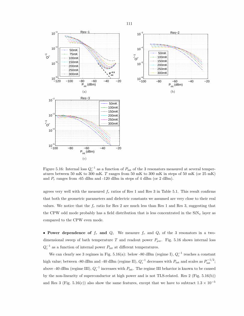
111
−120 −100 −80 −60 −40 −2010
−6
10−5
10−4
10−3
Pint
(dBm)
Qi−
1
Res−1
50mK 75mK100mK150mK200mK250mK300mK P
int−0.5
(a)
−100 −80 −60 −40 −2010
−6
10−5
10−4
10−3
Pint
(dBm)
Qi*−
1
Res−2
50mK100mK150mK200mK250mK300mK
(b)
−100 −80 −60 −40 −2010
−5
10−4
10−3
10−2
Pint
(dBm)
Qi*−
1
Res−3
50mK100mK150mK200mK250mK300mK
(c)
Figure 5.16: Internal loss Q−1i as a function of Pint of the 3 resonators measured at several temper-
atures between 50 mK to 300 mK. T ranges from 50 mK to 300 mK in steps of 50 mK (or 25 mK)and Pr ranges from -65 dBm and -120 dBm in steps of 4 dBm (or 2 dBm).
agrees very well with the measured fr ratios of Res 1 and Res 3 in Table 5.1. This result confirms
that both the geometric parameters and dielectric constants we assumed are very close to their real
values. We notice that the fr ratio for Res 2 are much less than Res 1 and Res 3, suggesting that
the CPW odd mode probably has a field distribution that is less concentrated in the SiNx layer as
compared to the CPW even mode.
• Power dependence of fr and Qi We measure fr and Qi of the 3 resonators in a two-
dimensional sweep of bath temperature T and readout power Pµw. Fig. 5.16 shows internal loss
Q−1i as a function of internal power Pint at different temperatures.
We can clearly see 3 regimes in Fig. 5.16(a): below -80 dBm (regime I), Q−1i reaches a constant
high value; between -80 dBm and -40 dBm (regime II), Q−1i decreases with Pint and scales as P
−1/2int ;
above -40 dBm (regime III), Q−1i increases with Pint. The regime III behavior is known to be caused
by the non-linearity of superconductor at high power and is not TLS-related. Res 2 (Fig. 5.16(b))
and Res 3 (Fig. 5.16(c)) also show the same features, except that we have to subtract 1.3 × 10⁻⁵
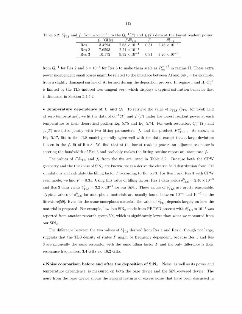
112
Table 5.2: δ0TLS and fr from a joint fit to the Q−1i (T ) and fr(T ) data at the lowest readout power
fr (GHz) Fδ0TLS F δ0TLS
Res 1 3.4294 7.63 × 10⁻⁴ 0.31 2.46 × 10⁻³
Res 2 7.6593 2.21 × 10⁻⁴ - -Res 3 10.172 9.92 × 10⁻⁴ 0.31 3.20 × 10⁻³
from Q−1i for Res 2 and 6 × 10⁻⁶ for Res 3 to make them scale as P
−1/2int in regime II. These extra
power independent small losses might be related to the interface between Al and SiNx—for example,
from a slightly damaged surface of Al formed during the deposition process. In regime I and II, Q−1i
is limited by the TLS-induced loss tangent δTLS which displays a typical saturation behavior that
is discussed in Section 5.4.5.2.
• Temperature dependence of fr and Qi To retrieve the value of δ0TLS (δTLS for weak field
at zero temperature), we fit the data of Q−1i (T ) and fr(T ) under the lowest readout power at each
temperature to their theoretical profiles Eq. 5.75 and Eq. 5.74. For each resonator, Q−1i (T ) and
fr(T ) are fitted jointly with two fitting parameters: fr and the product Fδ0TLS . As shown in
Fig. 5.17, fits to the TLS model generally agree well with the data, except that a large deviation
is seen in the fr fit of Res 3. We find that at the lowest readout powers an adjacent resonator is
entering the bandwidth of Res 3 and probably makes the fitting routine report an inaccurate fr.
The values of Fδ0TLS and fr from the fits are listed in Table 5.2. Because both the CPW
geometry and the thickness of SiNx are known, we can derive the electric field distribution from EM
simulations and calculate the filling factor F according to Eq. 5.73. For Res 1 and Res 3 with CPW
even mode, we find F = 0.31. Using this value of filling factor, Res 1 data yields δ0TLS = 2.46× 10⁻³
and Res 3 data yields δ0TLS = 3.2 × 10⁻³ for our SiNx. These values of δ0TLS are pretty reasonable.
Typical values of δ0TLS for amorphous materials are usually found between 10−4 and 10−2 in the
literature[59]. Even for the same amorphous material, the value of δ0TLS depends largely on how the
material is prepared. For example, low-loss SiNx made from PECVD process with δ0TLS ≈ 10−4 was
reported from another research group[59], which is significantly lower than what we measured from
our SiNx.
The difference between the two values of δ0TLS derived from Res 1 and Res 3, though not large,
suggests that the TLS density of states P might be frequency dependent, because Res 1 and Res
3 are physically the same resonator with the same filling factor F and the only difference is their
resonance frequencies, 3.4 GHz vs. 10.2 GHz.
• Noise comparison before and after the deposition of SiNx Noise, as well as its power and
temperature dependence, is measured on both the bare device and the SiNx-covered device. The
noise from the bare device shows the general features of excess noise that have been discussed in

113
0.05 0.1 0.15 0.2 0.25 0.32
3
4
5
6
7
8
x 10−4
T (K)
1/Q
iRes−1
datafit
(a)
0.05 0.1 0.15 0.2 0.25 0.3−0.5
0
0.5
1
1.5
2
2.5x 10
−4
T (K)
∆ f r/f r
Res−1
datafit
(b)
0.05 0.1 0.15 0.2 0.25 0.31.2
1.4
1.6
1.8
2
2.2
2.4x 10
−4
T (K)
1/Q
i
Res−2
datafit
(c)
0.05 0.1 0.15 0.2 0.25 0.3−15
−10
−5
0
5x 10
−6
T (K)
∆ f r/f r
Res−2
datafit
(d)
0.05 0.1 0.15 0.2 0.25 0.36
7
8
9
10
11
12x 10
−4
T (K)
1/Q
i
Res−3
datafit
(e)
0.05 0.1 0.15 0.2 0.25 0.3−6
−4
−2
0
2
4x 10
−5
T (K)
∆ f r/f r
Res−3
datafit
(f)
Figure 5.17: Joint fit of Q−1i and fr vs. T at lowest readout power into their theoretical profiles
Eq. 5.74 and Eq. 5.75
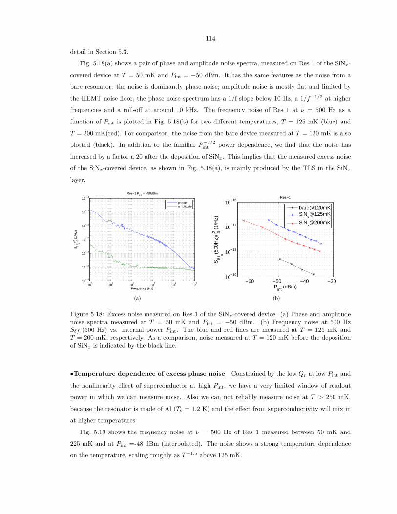
114
detail in Section 5.3.
Fig. 5.18(a) shows a pair of phase and amplitude noise spectra, measured on Res 1 of the SiNx-
covered device at T = 50 mK and Pint = −50 dBm. It has the same features as the noise from a
bare resonator: the noise is dominantly phase noise; amplitude noise is mostly flat and limited by
the HEMT noise floor; the phase noise spectrum has a 1/f slope below 10 Hz, a 1/f−1/2 at higher
frequencies and a roll-off at around 10 kHz. The frequency noise of Res 1 at ν = 500 Hz as a
function of Pint is plotted in Fig. 5.18(b) for two different temperatures, T = 125 mK (blue) and
T = 200 mK(red). For comparison, the noise from the bare device measured at T = 120 mK is also
plotted (black). In addition to the familiar P−1/2int power dependence, we find that the noise has
increased by a factor a 20 after the deposition of SiNx. This implies that the measured excess noise
of the SiNx-covered device, as shown in Fig. 5.18(a), is mainly produced by the TLS in the SiNx
layer.
100
101
102
103
104
105
10−20
10−19
10−18
10−17
10−16
10−15
10−14
Frequency (Hz)
Sδ
f 0/f 02 (1/
Hz)
Res−1 Pint
= −50dBm
phaseamplitude
(a)
−60 −50 −40 −3010
−19
10−18
10−17
10−16
Pint
(dBm)
Sδ
f 0(500
Hz)
/f 02 (1/
Hz)
Res−1
bare@120mKSiN
x@125mK
SiNx@200mK
(b)
Figure 5.18: Excess noise measured on Res 1 of the SiNx-covered device. (a) Phase and amplitudenoise spectra measured at T = 50 mK and Pint = −50 dBm. (b) Frequency noise at 500 HzSδfr (500 Hz) vs. internal power Pint. The blue and red lines are measured at T = 125 mK andT = 200 mK, respectively. As a comparison, noise measured at T = 120 mK before the depositionof SiNx is indicated by the black line.
•Temperature dependence of excess phase noise Constrained by the low Qr at low Pint and
the nonlinearity effect of superconductor at high Pint, we have a very limited window of readout
power in which we can measure noise. Also we can not reliably measure noise at T > 250 mK,
because the resonator is made of Al (Tc = 1.2 K) and the effect from superconductivity will mix in
at higher temperatures.
Fig. 5.19 shows the frequency noise at ν = 500 Hz of Res 1 measured between 50 mK and
225 mK and at Pint =-48 dBm (interpolated). The noise shows a strong temperature dependence
on the temperature, scaling roughly as T−1.5 above 125 mK.

115
101
102
103
10−18
10−17
10−16
T (mK)
Sδ
f r(500
Hz)
/f r2 (1/
Hz)
Res−1
Pint
=−48dBm
T−1.5
Figure 5.19: Temperature dependence of frequency noise measured on Res 1 at Pint = −48 dBmfrom the SiNx-covered device
Conclusion The measured temperature dependence of ∆fr/fr and Q−1i , as well as the power and
temperature dependence of Q−1i , all agree well with the TLS theory. By fitting the ∆fr(T )/fr data
and Qi(T )−1 data to Eq. 5.74 and Eq. 5.75, the product Fδ0TLS can be derived. If F is known, δ0TLS
can be determined, which is one of the important parameters of the TLS.
After the deposition of SiNx, the phase noise is seen to increase by a factor of 20. It also keeps
all the general features of phase noise found in a bare resonator. The fact that the noise from a
SiNx-covered device and from a bare device shows the same features is strong evidence that the
noise in both cases is of the same origin — TLS.
5.5.1.2 Nb microstrip with SiO2 dielectric on sapphire substrate
Another device we measured with a large TLS filling factor is a Nb on sapphire half-wavelength
microstrip resonator device. Between the top strip (600 nm thick) and the ground plane (150 nm
thick), both made of Nb, is a layer of sputtered (amorphous) SiO2 dielectric (400 nm thick). Other
relevant resonator parameters are listed in Table 5.3. Because the electric field is largely confined
in the dielectric layer, the microstrip should have a very high filling factor. Indeed, EM simulation
shows that F = 94% for this microstrip device.
• Power and temperature dependence of fr and Qi. We first measure the power and
temperature dependence of fr and Qi, and fit the latter to the TLS model to retrieve the value of
Fδ0TLS, as we did in the previous experiment with the SiNx-covered device.
The results are shown in Fig. 5.20. In Fig. 5.20(a) we plot a group of Q−1i vs. Pint curves at
different T , which looks very similar to its counter part in the SiNx experiment. In Fig. 5.20(b) we
plot a group of fr vs. T curves at different Pint, which shows the signature shape of TLS-induced
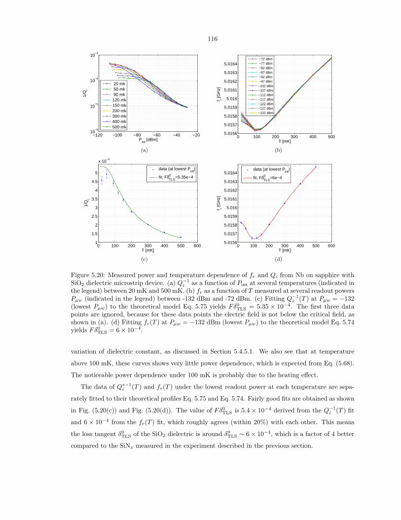
116
−120 −100 −80 −60 −40 −2010
−6
10−5
10−4
10−3
Pint
[dBm]
1/Q
i
20 mk 50 mk 90 mk120 mk150 mk200 mk300 mk400 mk500 mk
(a)
0 100 200 300 400 5005.0156
5.0157
5.0158
5.0159
5.016
5.0161
5.0162
5.0163
5.0164
T [mK]
f r [GH
z]
−72 dBm −77 dBm −82 dBm −87 dBm −92 dBm −97 dBm−102 dBm−107 dBm−112 dBm−117 dBm−122 dBm−127 dBm−132 dBm
(b)
0 100 200 300 400 500 6001
1.5
2
2.5
3
3.5
4
4.5
5
x 10−4
T [mK]
1/Q
i
data (at lowest Pint
)
fit, FδTLS0 =5.35e−4
(c)
0 100 200 300 400 500 6005.0156
5.0157
5.0158
5.0159
5.016
5.0161
5.0162
5.0163
5.0164
T [mK]
f r [GH
z]
data (at lowest Pint
)
fit, FδTLS0 =6e−4
(d)
Figure 5.20: Measured power and temperature dependence of fr and Qi from Nb on sapphire withSiO2 dielectric microstrip device. (a) Q−1
i as a function of Pint at several temperatures (indicated inthe legend) between 20 mK and 500 mK. (b) fr as a function of T measured at several readout powersPµw (indicated in the legend) between -132 dBm and -72 dBm. (c) Fitting Q−1
i (T ) at Pµw = −132(lowest Pµw) to the theoretical model Eq. 5.75 yields Fδ0TLS = 5.35 × 10⁻⁴. The first three datapoints are ignored, because for these data points the electric field is not below the critical field, asshown in (a). (d) Fitting fr(T ) at Pµw = −132 dBm (lowest Pµw) to the theoretical model Eq. 5.74yields Fδ0TLS = 6 × 10⁻⁴.
variation of dielectric constant, as discussed in Section 5.4.5.1. We also see that at temperature
above 100 mK, these curves shows very little power dependence, which is expected from Eq. (5.68).
The noticeable power dependence under 100 mK is probably due to the heating effect.
The data of Q∗−1i (T ) and fr(T ) under the lowest readout power at each temperature are sepa-
rately fitted to their theoretical profiles Eq. 5.75 and Eq. 5.74. Fairly good fits are obtained as shown
in Fig. (5.20(c)) and Fig. (5.20(d)). The value of Fδ0TLS is 5.4 × 10⁻⁴ derived from the Q−1i (T ) fit
and 6 × 10⁻⁴ from the fr(T ) fit, which roughly agrees (within 20%) with each other. This means
the loss tangent δ0TLS of the SiO2 dielectric is around δ0TLS ∼ 6 × 10⁻⁴, which is a factor of 4 better
compared to the SiNx measured in the experiment described in the previous section.
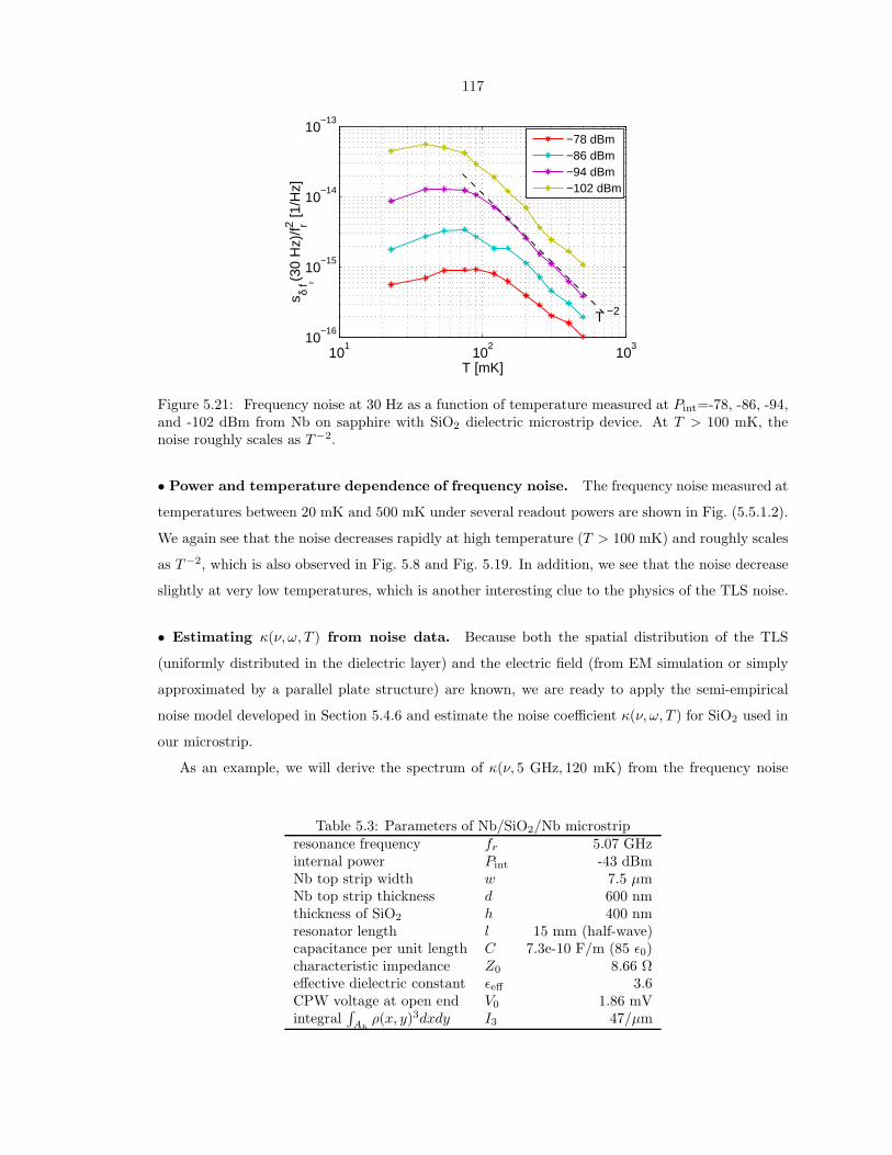
117
101
102
103
10−16
10−15
10−14
10−13
T [mK]
s δ f r(3
0 H
z)/f r2 [1
/Hz]
−78 dBm−86 dBm−94 dBm−102 dBm
T −2
Figure 5.21: Frequency noise at 30 Hz as a function of temperature measured at Pint=-78, -86, -94,and -102 dBm from Nb on sapphire with SiO2 dielectric microstrip device. At T > 100 mK, thenoise roughly scales as T−2.
• Power and temperature dependence of frequency noise. The frequency noise measured at
temperatures between 20 mK and 500 mK under several readout powers are shown in Fig. (5.5.1.2).
We again see that the noise decreases rapidly at high temperature (T > 100 mK) and roughly scales
as T−2, which is also observed in Fig. 5.8 and Fig. 5.19. In addition, we see that the noise decrease
slightly at very low temperatures, which is another interesting clue to the physics of the TLS noise.
• Estimating κ(ν, ω, T ) from noise data. Because both the spatial distribution of the TLS
(uniformly distributed in the dielectric layer) and the electric field (from EM simulation or simply
approximated by a parallel plate structure) are known, we are ready to apply the semi-empirical
noise model developed in Section 5.4.6 and estimate the noise coefficient κ(ν, ω, T ) for SiO2 used in
our microstrip.
As an example, we will derive the spectrum of κ(ν, 5 GHz, 120 mK) from the frequency noise
Table 5.3: Parameters of Nb/SiO2/Nb microstripresonance frequency fr 5.07 GHzinternal power Pint -43 dBmNb top strip width w 7.5 µmNb top strip thickness d 600 nmthickness of SiO2 h 400 nmresonator length l 15 mm (half-wave)capacitance per unit length C 7.3e-10 F/m (85 ǫ0)characteristic impedance Z0 8.66 Ωeffective dielectric constant ǫeff 3.6CPW voltage at open end V0 1.86 mVintegral
∫Ahρ(x, y)3dxdy I3 47/µm

118
spectrum measured at T = 120 mK and Pint = −38 dBm shown in Fig. 5.22(a). The 3 parameters,
C, V0, and l, required by Eq. 5.81 are calculated and listed in Table 5.3. The integral
I3 =
∫
Ah
ρ(x, y)3dxdy ≈ w/h2 (5.83)
is calculated by approximating the microstrip field with that in a parallel plate structure.
According to Eq. 5.81, the conversion factor from the frequency noise Sδfr (ν)/f2r to κ(ν, ω, T ) is
given by
g =4I3
3πC2V0l=
9.90 × 10⁷
ǫ20m−2V−1. (5.84)
By applying this factor, we finally derive the spectrum κ(ν, 5 GHz, 120 mK) which is shown in the
Fig. 5.22(b).
The noise coefficient κ(ν, ω, T ) for other temperatures T and microwave frequencies ω can be
derived in a similar way. Because on this device we have only one microstrip resonator with fr ∼5 GHz, we are unable to obtain κ for other frequencies. In future experiments, it should be easy
to design resonators which spread out in the wider frequency range in which we are interested. In
fact, according to the TLS picture, the frequency noise should be only dependent on the value of
~ω/kT , instead of ω and T individually. Once the values of κ(ν, ~ω/kT ) are derived, they can be
used to predict the frequency noise in resonators with any geometry, resonance frequency, and at
any temperature, as long as the TLS are of the same type, and the spatial distribution of the TLS
and the electric field are known in these resonators.
100
101
102
103
104
105
10−21
10−20
10−19
10−18
10−17
10−16
10−15
10−14
Frequency (Hz)
Sδ
f r/f r2 [1/H
z]
(a)
100
101
102
103
104
105
10−30
10−29
10−28
10−27
10−26
10−25
10−24
10−23
10−22
Frequency (Hz)
κ(ν,
5~
GH
z, 1
20~
mK
) ⋅ ε
02
(b)
Figure 5.22: Frequency noise spectrum (a) and the derived noise coefficient κ (b). The noise spectraare measured at T = 120 mK and Pint = −38 dBm from the Nb microstrip device with SiO2
dielectric.

119
5.5.2 Locating the TLS noise source
From the experimental and theoretical results presented in the preceding sections of this chapter,
we are almost certain that the excess noise is caused by fluctuating TLS in the dielectric materials.
So far we have not given any discussion on where the TLS are. As shown in Fig. 5.23, at least four
locations in our CPW resonator can host the TLS fluctuators—the bulk substrate or its exposed
surface, the interface layers between the metal films and the substrate, and the oxide layers on the
metal surfaces. In the next two experiments, we will give experimental evidence that the TLS are
distributed on the surface of the resonator but not in the bulk substrate.
Figure 5.23: Potential locations of TLS noise source: bulk substrate (yellow), exposed substratesurface (red), the interface layers between the metal films and the substrate (green), and oxidelayers on the metal surfaces (blue)
5.5.2.1 Evidence for a surface distribution of TLS from frequency shift measurement
We have learned a lot about the TLS effects on the dielectric properties from the study of SiNx-
covered device and SiO2 dielectric microstrip device. Especially, we are able to determine the
product of the TLS loss tangent δ0TLS and filling factor F by fitting the TLS models to either the
temperature dependence of ∆fr(T )/fr data at any readout power or Q−1i (T ) data at low power. In
this experiment, we go back and apply this analysis to study the intrinsic TLS in the bare resonators.
The key idea of this experiment is to measure ∆fr/fr of coplanar waveguide (CPW) resonators
with different geometries in order to obtain values of Fδ0TLS for each geometry. The frequency-
multiplexed resonators are all fabricated simultaneously and are integrated onto a single chip, and
are measured in a single cooldown. We can therefore safely assume that a single value of the loss
tangent δ0TLS applies for all resonator geometries. This allows the variation of the filling factor F
with geometry to be determined, providing information on the geometrical distribution of the TLS.
If TLS are in the bulk substrate with dielectric constant ǫr, Eq. 5.73 applied to the CPW field
distribution would yield a filling factor F ≈ ǫr/(ǫr +1) that is independent of the resonator’s center
strip width sr. If instead the TLS are in a surface layer, F should be dependent on the CPW
geometry, scaling roughly as 1/sr.
The geometry test device used in this experiment consists of five CPW quarter-wavelength res-
onators with different geometries. They are patterned from a 120 nm-thick Nb film deposited on a

120
Figure 5.24: An illustration of the CPW coupler and resonator. The inset shows a cross-sectionalview of the CPW. The contour of the metal surface and the contour of the exposed surface of thesubstrate are indicated by the solid line and the dashed line, respectively.
crystalline sapphire substrate. Because Nb has a critical temperature Tc = 9.2 K, the effect of super-
conductivity on the temperature dependence of the resonance frequency is negligible for T < 1 K.
As shown in Fig. 5.24, each resonator is capacitively coupled to a common feedline using a CPW
coupler of length lc ∼= 200 µm and with a common center-strip width of sc = 3 µm. The coupler is
then widened into the resonator body, with a center-strip width of sr = 3 µm, 5 µm, 10 µm, 20 µm
or 50 µm, and a length of lr ∼ 5 mm. The ratio between center strip width s and the gap g in both
the coupler and the resonator body is fixed to 3:2, to maintain a constant impedance of Z0 ≈ 50 Ω.
The resonance frequencies are fr ∼ 6 GHz, and the coupler is designed to have a coupling quality
factor Qc ∼ 50, 000.
Fig. 5.25 shows the measured frequency shifts ∆fr/fr for the five resonators as a function of
temperature over the temperature range 100 mK to 800 mK. Although all of the resonators display
a common shape for the variation of frequency with temperature, the magnitude of the effect varies
strongly with geometry. As shown by the dashed lines in Fig. 5.25, fits to the TLS model (Eq. 5.74)
generally agree quite well with the data. The familiar non-monotonic variation of the dielectric
constant with temperature can be clearly seen in Fig. 5.25: fr increases (ǫ decreases) when T >
~ω/2k; a minimum in fr (a maximum in ǫ) occurs around T = ~ω/2k; at lower temperatures (T <
100 mK), we would expect to see a decrease in fr (increase in ǫ) as indicated by the extrapolation
of the fit. The largest deviations from the TLS model (about 4%) occur at the lowest temperatures,
and are likely due to TLS saturation effects discussed in Section 5.4.5.2. Power-dependent frequency
shifts of this size have also been previously observed experimentally[63]. Here, we will ignore these
small effects and focus on the geometrical dependence.
With the exception of the 3 µm resonator, the measured values of Fδ0TLS from the fits have to
be corrected for the coupler because the coupler’s center strip width sc = 3 µm differs from that

121
100 200 300 400 500 600 700 800−12
−10
−8
−6
−4
−2
0
x 10−6
T (mK)
∆ fr/
f r
3 µm
5 µm
10 µm
20 µm
50 µm
Figure 5.25: Fractional frequency shift ∆fr/fr as a function of temperature. ∆fr/fr is calculatedusing ∆fr/fr = [fr(T ) − fr(800 mK)]/fr(800 mK). The temperature sweep is in steps of 50 mKfrom 100 mK to 600 mK, and in steps of 100 mK above 600 mK. The markers represent differentresonator geometries, as indicated by the values of the center strip width sr in the legend. Thedashed lines indicate fits to the TLS model.
of the resonator, sc 6= sr. In the limit lc << lr, it can be shown that the corrected filling factor is
given by,
F ∗ =F − tF3µm
1 − t(5.85)
where t = 2lc/(lc + lr). The values of F ∗δ0TLS are listed in Table 5.4, as well as the ratios relative to
the value for 3 µm resonator.
We also measured the resonance frequencies at 4.2 K (0.46 Tc), allowing the shift ∆fr(4.2 K) =
fr(4.2 K)−fr(100 mK) as well as the kinetic inductance fraction to be calculated for each geometry,
as shown in Table 5.4.
Fig. 5.26 shows the results for the geometrical scaling of the corrected filling factor F ∗ and the
kinetic inductance fraction α, plotted as ratios relative to their respective values for the resonator
with a 3 µm wide center strip. The observed strong variation of F ∗ with geometry immediately rules
out a volume TLS distribution, and favors a surface distribution. We investigate this in more detail
by comparing the data to two theoretically calculated geometrical factors gm and gg, which have
units of inverse length and are calculated from contour integrals in a cross-sectional plane given by
gm =1
V 2
∫
metal
~E2dl (5.86)
gg =1
V 2
∫
gap
~E2dl (5.87)
where V is the CPW voltage. The first integral is actually a sum of three contour integrals, taken
over the surfaces of the three metal conductors, the center strip and the two ground planes. The

122
0.1
1
ratios
3 5 10 20 50
0.8
1
1.2
(µm)
r i
r1=α /α
3µmr2=
*/
*3µm
r3=
m/
m,3µmr4=
g/
g,3µm
/r1
sr
g g g g
F F
Figure 5.26: The scaling of the measured values of the kinetic inductance α and TLS filling factorF ∗, as well as the calculated values of the CPW geometrical factors gm and gg, are shown, as afunction of the resonator center strip width sr. The top panel shows the ratios of α (r1), F
∗ (r2),gm (r3), and gg (r4) to their values for the 3 µm resonators. The bottom panel shows these ratiosnormalized by the kinetic inductance ratio r1.
second contour integral is taken over the two “gaps”, the surface of the exposed substrate in between
the conductors. These contours are illustrated in the inset of Fig. 5.24. The integrals are evaluated
numerically using the electric field derived from a numerical conformal mapping solution to the
Laplace equation, where the conformal mapping procedure is identical to that used in the calculation
of α described in Section 3.1.3.1.
According to Eq. 5.73, F ∗ should have the same scaling as gm if the TLS are distributed on the
metal surface (or at the metal-substrate interface), or as gg if the TLS are located on the surface of
the exposed substrate. The kinetic inductance of the CPW may also be calculated using a contour
integral similar to that of gm, except that the integrand is replaced by ~H2[64]. Because the magnetic
field ~H is proportional to ~E for a quasi-TEM mode, we expect the kinetic inductance fraction α to
have the same geometrical scaling as gm.
Fig. 5.26 shows that the four quantities, F ∗, α, gm, and gg, all scale as s−γr with γ = 0.85− 0.91.
The finite thickness of the superconducting film is responsible for the deviations from γ = 1. This
is very strong evidence that the TLS have a surface distribution and are not uniformly distributed
in the bulk substrate. These data, however, cannot discriminate between a TLS distribution on
the metal surface and a TLS distribution on the exposed substrate surface (the gap), because the
corresponding theoretical predictions (gm and gg) are very similar and both agree with the data.
Future measurements of resonators with various center-strip-to-gap ratios may allow these two TLS
distributions to be separated.
The absolute values of F ∗δ0TLS are also of interest. Assuming a typical value of δ0TLS ∼ 10−2 for
the TLS-loaded material[59], the measured value of F ∗δ0TLS = 3×10⁻⁵ for the 3 µm resonator yields

123
a filling factor of F ∗ ∼ 0.3%. Numerical calculations show that this is consistent with a ∼ 2 nm layer
of the TLS–loaded material on the metal surface or a ∼ 3 nm layer on the gap surface, suggesting
that native oxides or adsorbed layers may be the TLS host material[72].
Table 5.4: Values and ratiossr fr(100 mK) ∆fr(4.2 K) α
α3µmF ∗δ0TLS
F∗
F∗3µm
gm
gm,3µm
gg
gg,3µm
[µm] [GHz] [MHz] ×10−5
3 µm 5.666 11.1 1 2.98 ± 0.12 1 1 15 µm 5.735 7.41 0.67 2.00 ± 0.07 0.67 0.62 0.6410 µm 5.800 4.15 0.37 1.10 ± 0.03 0.37 0.33 0.3520 µm 5.836 2.28 0.21 0.54 ± 0.03 0.18 0.17 0.1950 µm 5.851 1.02 0.092 0.24 ± 0.02 0.08 0.075 0.086
5.5.2.2 More on the geometrical scaling of frequency noise
100
101
102
103
104
105
10−21
10−20
10−19
10−18
10−17
10−16
/fr2 [1/Hz]
ν [Hz]−30 −25 −20 −15
10−19
10−18
Pint [dBm]
Sδf r (2 kHz)
f r2 [1/Hz]
3 µm
5 µm
10 µm
20 µm
/(a) (b)
Sδ
rf
Figure 5.27: Frequency noise of the four CPW resonators measured at T = 55 mK. (a) Frequencynoise spectra at Pµw = −65 dBm. From top to bottom, the four curves correspond to CPW centerstrip widths of sr = 3 µm, 5 µm, 10 µm, and 20 µm. The various spikes seen in the spectra aredue to pickup of stray signals by the electronics and cabling. (b) Frequency noise at ν = 2 kHz asa function of Pint. The markers represent different resonator geometries, as indicated by the valuesof sr in the legend. The dashed lines indicate power law fits to the data of each geometry.
In addition to the low-temperature frequency shift data, we also measured the frequency noise
data on the same geometry test device as described in the previous section in the same cooldown.
The frequency noise spectra Sδfr (ν)/f2r of the five resonators are measured for microwave readout
power Pµw in the range -61 dBm to -73 dBm. As an example, the frequency noise spectra measured
at Pµw = −65 dBm are shown in Fig. 5.27(a). Apart from a common spectral shape, we clearly see
that the level of the noise decreases as the center strip becomes wider. Unfortunately the noise of
the 50 µm-resonator is not much higher than that of our cryogenic HEMT amplifier, and therefore
those measurements are less reliable, so we exclude the 50 µm-resonator from further discussion.

124
3 5 10 2010
−20
10−19
10−18
s [µm]
Sδf
r (2
kHz)
/f2 r [1/
Hz]
uncorrectedcorrected
s−1.58
Figure 5.28: The measured frequency noise Sδf (2 kHz)/f2r at Pint = −25 dBm is plotted as a
function of the center strip width sr. Values directly retrieved from power-law fits to the data inFig. 5.27 are indicated by the open squares. Values corrected for the coupler’s contribution areindicated by the stars. The corrected values of Sδf (2 kHz)/f2
r scale as s−1.58r , as indicated by the
dashed line.
The noise levels at ν =2 kHz were retrieved from the noise spectra and are plotted as a function
of resonator internal power Pint = 2Q2rPµw/πQc in Fig. 5.27(b). All resonators display a power
dependence close to Sδf/f2r ∝ P
−1/2int , as we have previously observed[73, 70, 63]. In order to
study the geometrical scaling of the noise in more detail, we first fit the noise vs. power data
for each resonator to a simple power law, and retrieve the values of the noise Sδf (2 kHz)/f2r at
Pint = −25 dBm for each geometry. These results (Fig. 5.28) again show that the noise decreases
with increasing sr, although not (yet) as a simple power law.
To make further progress, we apply the semi-empirical noise model (Eq. 5.80) to the coupler
correction. For the resonators that are wider than the coupler (sr > sc = 3 µm), the measured
values of Sδfr/f2r need to be corrected for the coupler’s noise contribution. A similar procedure was
applied in the frequency shift data in the previous section (Eq. 5.85). In the limit lc << lr, the
correction is given by
S∗δfr
= (Sδfr − ηSδfr , 3µm)/(1 − η) (5.88)
where η = 3πlc/4(lc + lr). The corrected values are plotted in Fig. 5.28 (with symbol stars) and
are found to have a simple power–law scaling 1/s1.58r . We find a similar noise scaling, 1/sα
r , with α
between 1.49 and 1.6, for noise frequencies 400 Hz < ν < 3 kHz.
While the fact that an |E|3–weighted coupler noise correction leads to a simple power law noise
scaling is already quite encouraging, we will now go further and show that the observed s−1.58r power–
law slope can be reproduced by our semi-empirical noise model. Measurements of the anomalous

125
0.001 0.01 0.1 10
100
t/sr
Fm(t
/sr)
β=0.28, γ=−0.440
β=0.33, γ=−0.452
β=0.38, γ=−0.456
β=0.43, γ=−0.4553
Figure 5.29: The calculated dimensionless noise scaling function Fm3 (t/sr) is plotted as a function of
the ratio between the CPW half film thickness t and the center strip width sr. The inset shows theconformal mapping used to derive the electric field. The contour integral for Fm
3 (t/sr) is evaluatedon the surface of the metal, as outlined by the solid lines in the W -plane. Results are shown for fourdifferent values of the parameter β = 0.28, 0.33, 0.38, 0.43 that controls the edge shape (see inset).The dashed lines indicate power law (t/sr)
γ fits to Fm3 (t/sr).
low temperature frequency shift described in the previous section have already pointed to a surface
distribution of TLS. If these TLS are also responsible for the frequency noise, according to Eq. 5.80
we would expect the noise to have the same geometrical scaling as the contour integral I3 =∫| ~E|3ds
evaluated either on the metal surface (Im3 ) or the exposed substrate surface (Ig
3 ). For zero-thickness
CPW, although the integral is divergent, the expected scaling can be shown to be I3 ∝ 1/s2r. For
CPW with finite thickness, we can evaluate I3 numerically using the electric field derived from a
numerical conformal mapping solution. The two-step mapping procedure used here is modified from
that given by Collin[55] and is illustrated in the inset of Fig. 5.29. We first map a quadrant of
finite-thickness CPW with half thickness t ( in the W -plane) to a zero-thickness CPW (in the Z-
plane) and then to a parallel-plate capacitor (in the ξ-plane). To avoid non-integrable singularities,
we must constrain all internal angles on the conductor edges to be less than π/2, which leads to
the condition 0.25 < β < 0.5, where βπ is the angle defined in Fig. 5.29. Instead of evaluating I3
directly, we define a normalized dimensionless integral F3(t, sr) =∫| ~E/E∗|3ds∗, where s∗ = s/sr is
a normalized integration coordinate and E∗ = V/sr is a characteristic field strength for a CPW with
voltage V . Now F3 depends only on the ratio t/sr and is related to the original contour integral by
I3(sr, t, V ) = (V 3/s2r)F3(t/sr). The results Fm3 (t/sr) calculated for the metal surface are plotted
in Fig. 5.29, and show a power law scaling Fm3 ∼ (t/sr)
γ with γ ≈ −0.45 for 0.003 < t/sr < 0.02,
the relevant range for our experiment. We also find that for a wide range of β, 0.27 < β < 0.43,
although the absolute values of Fm3 (t/sr) vary significantly, the scaling index γ remains almost
constant, −0.456 < γ < −0.440. Therefore, γ appears to depend little on the edge shape.

126
From Eq. 5.80, the noise scaling is predicted to be Im3 (t, sr, V ) ∝ s−2−γ
r ∼ s−1.55r (at fixed
V ), which agrees surprisingly well with the measured s−1.58r scaling. We also investigated the case
for TLS located on the exposed substrate surface, and found that F g3 has almost identical scaling
(γ ≈ −0.45) as Fm3 . While we still cannot say whether the TLS are on the surface of the metal
or the exposed substrate, we can safely rule out a volume distribution of TLS fluctuators in the
bulk substrate; this assumption yields a noise scaling of ∼ s−1.03r , significantly different than that
measured.
In summary, the scaling of the frequency noise with resonator power and CPW geometry can
be satisfactorily explained by the semi-empirical model developed in Section 5.4.6 and with the as-
sumption of a surface distribution of independent TLS fluctuators. These results allow the resonator
geometry to be optimized, which will be discussed in the next section. Had we known the exact
~E field distribution and the exact TLS distribution for our CPW resonators, we would be able to
derive the noise coefficient κ(ν, ω, T ) as we did for the SiQ2 microstrip experiment discussed earlier.
Unfortunately, the two parameters, the edge shape and the thickness of the TLS layer, required for
calculating κ(ν, ω, T ) are not easily available. However, they are expected to be common among
resonators fabricated simultaneously on the same wafer, and more or less stable for resonators fab-
ricated through the same processes. Since we have shown that the ratio of | ~E|3 integral between
two resonator geometries is insensitive to the edge shape, we can still predict the scaling of the noise
among different resonator geometries[74].
5.6 Method to reduce the noise
Based on our knowledge of the excess noise, we propose several methods that may potentially reduce
the noise. Some of them have already been put into the action and proved to be effective. Of course,
a better understanding of the physics of the TLS noise may lead to more effective noise reduction
methods.
5.6.1 Hybrid geometry
5.6.1.1 Two-section CPW
Our noise model (Eq. 5.80) implies that the noise contributions are weighted by | ~E|3, so TLS
fluctuators located near the coupler end of a quarter-wave resonators should give significantly larger
noise contributions than those located near the shorted end. Meanwhile, the noise measurement
of the geometry test device has demonstrated that the noise decreases rapidly with increasing sr,
scaling as s−1.6r . This leads us to a two-section CPW resonator design for MKID. As shown in
Fig. 5.30, the resonator has a wider section (with center strip width s1, gap g1, and length l1) on
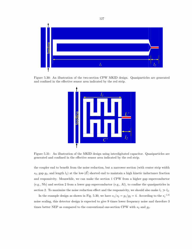
127
1 2
Figure 5.30: An illustration of the two-section CPW MKID design. Quasiparticles are generatedand confined in the effective sensor area indicated by the red strip.
2
1
Figure 5.31: An illustration of the MKID design using interdigitated capacitor. Quasiparticles aregenerated and confined in the effective sensor area indicated by the red strip.
the coupler end to benefit from the noise reduction, but a narrower section (with center strip width
s2, gap g2, and length l2) at the low-| ~E| shorted end to maintain a high kinetic inductance fraction
and responsivity. Meanwhile, we can make the section 1 CPW from a higher gap superconductor
(e.g., Nb) and section 2 from a lower gap superconductor (e.g., Al), to confine the quasiparticles in
section 2. To maximize the noise reduction effect and the responsivity, we should also make l1 ≫ l2.
In the example design as shown in Fig. 5.30, we have s1/s2 = g1/g2 = 4. According to the s−1.6r
noise scaling, this detector design is expected to give 9 times lower frequency noise and therefore 3
times better NEP as compared to the conventional one-section CPW with s2 and g2.
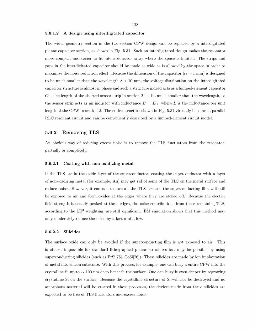
128
5.6.1.2 A design using interdigitated capacitor
The wider geometry section in the two-section CPW design can be replaced by a interdigitated
planar capacitor section, as shown in Fig. 5.31. Such an interdigitated design makes the resonator
more compact and easier to fit into a detector array where the space is limited. The strips and
gaps in the interdigitated capacitor should be made as wide as is allowed by the space in order to
maximize the noise reduction effect. Because the dimension of the capacitor (l1 ∼ 1 mm) is designed
to be much smaller than the wavelength λ > 10 mm, the voltage distribution on the interdigitated
capacitor structure is almost in phase and such a structure indeed acts as a lumped-element capacitor
C′. The length of the shorted sensor strip in section 2 is also much smaller than the wavelength, so
the sensor strip acts as an inductor with inductance L′ = Ll1, where L is the inductance per unit
length of the CPW in section 2. The entire structure shown in Fig. 5.31 virtually becomes a parallel
RLC resonant circuit and can be conveniently described by a lumped-element circuit model.
5.6.2 Removing TLS
An obvious way of reducing excess noise is to remove the TLS fluctuators from the resonator,
partially or completely.
5.6.2.1 Coating with non-oxidizing metal
If the TLS are in the oxide layer of the superconductor, coating the superconductor with a layer
of non-oxidizing metal (for example, Au) may get rid of some of the TLS on the metal surface and
reduce noise. However, it can not remove all the TLS because the superconducting film will still
be exposed to air and form oxides at the edges where they are etched off. Because the electric
field strength is usually peaked at these edges, the noise contributions from these remaining TLS,
according to the | ~E|3 weighting, are still significant. EM simulation shows that this method may
only moderately reduce the noise by a factor of a few.
5.6.2.2 Silicides
The surface oxide can only be avoided if the superconducting film is not exposed to air. This
is almost impossible for standard lithographed planar structures but may be possible by using
superconducting silicides (such as PtSi[75], CoSi[76]). These silicides are made by ion implantation
of metal into silicon substrate. With this process, for example, one can bury a entire CPW into the
crystalline Si up to ∼ 100 nm deep beneath the surface. One can bury it even deeper by regrowing
crystalline Si on the surface. Because the crystalline structure of Si will not be destroyed and no
amorphous material will be created in these processes, the devices made from these silicides are
expected to be free of TLS fluctuators and excess noise.

129
5.6.3 Amplitude readout
As has been shown earlier in this chapter, no excess noise is observed in the amplitude direction and
the amplitude noise, set by the noise temperature of HEMT, can be orders of magnitude lower than
the phase noise at low noise frequencies. Therefore, using amplitude readout may avoid the excess
noise and in some cases give better sensitivity.
Recall from Chapter 2 and 4 that a change in the quasiparticle will cause a change in both the
real (σ1) and imaginary (σ2) part of the conductivity, resulting in an IQ trajectory that is always
at a nonzero angle ψ = tan−1(δσ1/δσ2) to the resonance circle. Calculation from Martis-Bardeen’s
theory shows that tanψ = 1/4 ∼ 1/3 for the temperature and frequency range that MKIDs usually
operate in. This means as soon as the phase noise exceeds the amplitude noise (HEMT noise floor)
by about a factor of 10 (in power), amplitude readout may yield a better NEP than the phase
readout.
0 1 0 0 2 0 0 3 0 0 4 0 0 5 0 0 6 0 0 7 0 0 8 0 0 9 0 0 1 0 0 00
2 0 0
4 0 0
6 0 0
8 0 0
1 0 0 0
1 2 0 0
Tim e ( 4! s )
Puls
e h
eig
ht
Figure 5.32: Detector response to a single UV photon event. The data is measured from a 40 nmAl on sapphire MKID illuminated by monochromatic UV photons (λ = 254 nm) at around 200 mK.The quasi-particle recombination time is measured to be 20 µs. The inset shows the resonance circleand the pulse response in the IQ plane. In the zoom-in view of the pulse response, one can identifythe pulse and the noise ellipse. The angle between the average pulse direction and the major axisof the noise ellipse is 15.
Fig. 5.32 shows the measured detector response to a 254 nm UV photon. From the average pulse
trajectory and the major axis of the noise ellipse, we determine ψ ≈ 15. Applying the standard
optimal filtering analysis to these data, we derived the NEP for both the phase and amplitude
readout, which is plotted in Fig. 5.33. We see that amplitude NEP is a factor of 4 lower than the
phase NEP at low frequency (below 10 Hz). At high frequency (above 5 kHz), the phase NEP
becomes better than the amplitude NEP again. To take advantage of the signal in both directions,
one can analyze the data using a two-dimensional optimal filtering algorithm. It can be shown that

130
100
101
102
103
104
105
10−17
10−16
10−15
NE
P [W
⋅ Hz−
1/2 ]
Freqeuncy [Hz]
NEP PhaseNEP AmplitudeNEP 2D
Figure 5.33: NEP calculated for the phase readout (blue), amplitude readout (green), and a combinedreadout (red)
the two-dimensional NEP is given by
NEP−22D = NEP−2
pha + NEP−2amp (5.89)
which is indicated by the lowest curve in Fig. 5.33.
131
Chapter 6
Sensitivity of submm kineticinductance detector
In this chapter, we will discuss the sensitivity of submm MKIDs, as an example of applying the
models and theories of superconducting resonators developed in the previous chapters.
As the first stage of the detector development, these submm MKIDs are to be deployed in the
Caltech Submillimeter Observatory (CSO), a ground-based telescope. For ground-based observa-
tions, it is inevitable that the detector will be exposed to the radiations from the atmosphere and
have a background photon signal. Once the intrinsic noise of the detector is made smaller than
the shot noise of this background photon signal, the sensitivity of the detector is adequate. This
requirement is called background limited photon (BLIP) detection.
One of the important questions to be answered in this chapter is whether our submm MKIDs
can achieve the background limited photon detection on the ground, or in other words, whether the
intrinsic detector noise (g-r noise, HEMT amplifier noise, and TLS noise) is below the photon noise
of the background radiation from the atmosphere.
6.1 The signal chain and the noise propagation
In our submm MKID design, we have adopted the hybrid resonator architecture as discussed in
Section 4.4, Section 5.6.1, and shown in Fig. 5.30.
For the purpose of a sensitivity analysis, the signal chain of the detector is illustrated in Fig. 6.1:
the submm photon stream (with optical power p) breaks the Cooper pairs and generates quasipar-
ticles (with density nqp), which changes the impedance of the sensor strip Zl and the microwave
output signal V −2 (the microwave voltage seen at the input port of the HEMT). We would like to
derive the fluctuations in the output voltage δV −2 when the sensor strip is under the optical loading
p.

132
( )
( )
( )p
p t
p t
S
( )
( )
( )qp
qp
qp
n
n t
n t
S
( )
( )
( )L
L
L
z
z t
z t
S2
2
2
( )
( )
( )V
V t
V t
S
Figure 6.1: A diagram of the signal chain and noise propagation in a hybrid submm detector.p: optical power; Zl: load impedance of the sensor strip nqp: quasiparticle density; V −
2 : outputmicrowave voltage seen at the input port of the HEMT
6.1.1 Quasiparticle density fluctuations δnqp under an optical loading p
When the sensor strip is under optical loading, the total quasiparticle density nqp is the sum of
the thermal quasiparticle density nthqp (generated by thermal phonons) and the excess quasiparticle
density nexqp (generated by optical photons).
nqp = nthqp + nex
qp (6.1)
Three independent physical processes are involved in changing nqp and must be modeled: thermal
quasiparticle generation, excess quasiparticle generation, and quasiparticle recombination. We can
write out the following rate equation,
dnqp(t)
dt= [gth(t) + gex(t) − r(t)] (6.2)
where gth(t), gex(t), and r(t) are the rates for the 3 processes.
6.1.1.1 Quasiparticle recombination r(t)
The average quasiparticle recombination rate only depends on the total quasiparticle density nqp
and is calculated by[77]
〈r(t)〉 = r(nqp) = Rn2qp. (6.3)
With this definition, the quasiparticle lifetime is given by1
1
τqp(nqp)= 2Rnqp (6.4)
1We usually express the quasiparticle lifetime as τ−1qp = τ−1
0+2Rnqp, to account a finite lifetime τ0 at low nqp. In
the regime that submm MKIDs operate, nqp from the background loading is usually large enough so that the Rnqp
term will dominate over the τ−1
0term. For this reason, we ignore the τ−1
0term throughout the calculations in this
chapter.

133
where R is the recombination constant.
We write
r(t) =2R(t)
V= 〈r(t)〉 + δr(t) (6.5)
where V is the volume of the sensor strip and R(t) represents the recombination events in the volume
V . R(t) is often modeled by a Poisson point process[78] and it can be shown that the auto-correlation
function of δr(t) is a delta function
< δr(t)δr(t′) > =4
V 2〈R(t)〉 δ(t− t′) =
2
VRn2
qpδ(t− t′) (6.6)
and the power spectrum is white
Sδr(f) =2
VRn2
qp. (6.7)
6.1.1.2 Thermal quasiparticle generation gth(t)
The average thermal generation rate only depends on the bath temperature T and is in balance
with the thermal recombination rate when the system is in thermal equilibrium and without excess
quasiparticles
⟨gth(t)
⟩= gth(T ) = r(nth
qp(T )) = Rnthqp(T )2 (6.8)
where nthqp is the thermal quasiparticle density given by Eq. 2.93.
We write
gth(t) =2Gth(t)
V=⟨gth(t)
⟩+ δgth(t) (6.9)
where Gth(t) represents the thermal generation events, which is also modeled by a Poisson point
process. The power spectrum of δgth(t) is
Sδgth(f) =2
VRnth
qp(T )2. (6.10)
6.1.1.3 Excess quasiparticle generation gex(t) under optical loading
We assume that the number of excess quasiparticles generated by each detected submm photon
is given by ζ(ν,∆), which in general, depends both on the photon energy hν and the gap energy
∆ (binding energy of the Cooper pair). An empirical assumption about ζ(ν,∆) often adopted for
photon to quasiparticle conversion is that a fraction of ηe ≈ 60% of the photon energy goes to the

134
quasiparticles,
ηe =ζ∆
hν(6.11)
Thus, the excess quasiparticle generation rate gex(t) and the photon detection rate Gph(t) (num-
ber of photons detected per unit time) are related by
gex(t) =ζ
VGph(t). (6.12)
The statistical properties of Gex(t) can be found in photon counting theory. In addition, to
simplify the discussion, we make the following assumptions:
1. The optical loading is from the black body radiation with mean photon occupation number
nph = (ehνkT − 1)−1;
2. The photon numbers and their fluctuations of different modes are independent;
3. The detector has a narrow band of response (∫dν → ∆ν);
4. The detector is single mode (AΩ = λ2, where A is the area of the detector and Ω is diffraction
limited solid angle) and is only sensitive to one of the two polarizations;
5. The detector has a quantum efficiency of 1. (A reduced quantum efficiency η can be introduced
with the substitution nph → ηnph.)
Under these assumptions, we can derive
< Gph(t) >= ∆νnph (6.13)
p =< Gph(t) > hν = ∆νnphhν (6.14)
< δGph(t)δGph(t′) >= ∆νnph(1 + nph)δ(t− t′) (6.15)
where p is the average optical power received by the detector. Therefore
〈gex(t)〉 = gex(p) =ζ
V∆νnph =
ζp
hνV(6.16)
Sδgex(f) =
(ζ
V
)2
∆νnph(1 + nph) =
(ζ
V
)2p
hν(1 +
p
hν∆ν). (6.17)
6.1.1.4 Steady state quasiparticle density nqp
The steady state quasiparticle density nqp can be derived by solving
dnqp(t)
dt= 0 (6.18)

135
which leads to a quadratic equation
Rn2qp −Rnth
qp(T )2 − ζp
hνV= 0. (6.19)
We usually operate at a low enough temperature so that the excess quasiparticle generation rate
dominates over the thermal quasiparticle generation rate
gex(p) ≫ gth(T ). (6.20)
Under this condition, the thermal generation terms can be neglected and the steady-state equation
reduces to,
Rn2qp =
ζp
hνV(6.21)
and the positive root is
nqp =
√ζp
hνRV(6.22)
6.1.1.5 Fluctuations in quasiparticle density δnqp
The fluctuations in the quasiparticle density δnqp(t) = nqp(t) − nqp can be shown to satisfy the
following equation,
dδnqp(t)
dt= −2Rnqpδnqp(t) + [δgth(t) + δgex(t) − δr(t)] (6.23)
This allows us to calculate the power spectrum of δnqp in the Fourier domain as,
Sδnqp(f) =τ2qp
1 + (2πfτqp)2[Sδgth(f) + Sδgex(f) + Sδr(f)] =
τ2qp
1 + (2πfτqp)2Sgr(f) (6.24)
where τqp = τqp(nqp) and we have used the fact that the 3 processes are independent. Under the
condition that the excess quasiparticle generation dominates over thermal generation,
Sgr(f) ≈ Sδr(f) + Sδgex(f)
≈ 2ζp
hνV 2+
(ζ
V
)2p
hν(1 +
p
hν∆ν) (6.25)
where Eq. 6.14 and Eq. 6.21 have been applied. By applying Eq. 6.3 and Eq. 6.22 we can further
derive the spectral density of the fractional quasiparticle density fluctuations,
S δnqpnqp
(f) =Sδnqp(f)
n2qp
=1/4
1 + (2πfτqp)2
[(2/ζ + 1)hν
p+
1
∆ν
]. (6.26)
136
Note that the power spectra derived above are double-sided with −∞ < f <∞.
6.2 Noise equivalent power (NEP)
Now we are ready to calculate NEP of our submm MKIDs limited by different noise sources.
Throughout the derivation that follows, we make the assumption that the noise frequency f of
interest is small compared to both the resonator bandwidth f ≪ fr/2Qr and the recombination
bandwidth f ≪ fr/2πτqp.
We also assume that the maximum microwave power allowed to be dissipated in the sensor strip
equals the submm optical power absorbed in the sensor strip times a fudge factor ξ ≥ 12
Pl = ξηep. (6.27)
This ensures that the microwave readout power will not overwhelm the optical power in generating
quasiparticles and so the quasi-particle population in the sensor strip is always dominated by the
submm photon generated quasiparticles. For simplicity, we assume ξ = 1 in future derivations.
6.2.1 Background loading limited NEP
The directive of the logarithm of Eq. 6.21 yields a very simple and useful relationship
dnqp/nqp
dp=
1
2p. (6.28)
The background loading limited NEP can be calculated by
NEPBLIP(f) =√SBLIP
δnqp/nqp(f)
∣∣∣∣dnqp/nqp
dp
∣∣∣∣−1
(6.29)
=
√(2
ζhν + hν +
p
∆ν
)p
=
√(2∆
ηe+ hν +
p
∆ν
)p (6.30)
where Eq. 6.26 and Eq. 6.11 have been used.
2In theory, the microwave frequency (< 10 GHz) is far below the gap frequency of Al (∼90 GHz) and can notdirectly break Cooper pairs. However, in experiments we have observed both a shift in the resonance frequency and adecrease in the quality factor as the microwave power increases, which suggests that the microwave power (dissipatedby the surface resistance) is able to increase the quasiparticle density in the superconductor through some unknownmechanism. Because part (perhaps most part) of this dissipated microwave power goes to the phonon bath, the fudgefactor must be larger (perhaps much larger) than 1.
137
6.2.2 Detector NEP limited by the HEMT amplifier
The HEMT noise temperature Tn is equivalent to a voltage fluctuation δV2− seen at the input port
of the HEMT, with the noise power spectrum given by
SHEMTδV2−
(f + f) = kTnZ0 (6.31)
which, after IQ demodulation, leads to a (isotropic) noise
SHEMTIQ (f) = kTnZ0/2 (6.32)
in either the phase or amplitude quadrature of the IQ voltage output. In order to calculate NEP
utilizing Eq. 6.28, we would like to convert the HEMT noise to an equivalent fluctuation in the
quasiparticle density δnqp/nqp.
In Section 4.4, we have discussed the the dynamic response of a hybrid resonator. According to
Eq. 4.73 and 4.58, under the optimal condition (which maximizes the responsivity)
Qc = Qi and f = fr (6.33)
the spectrum of the fluctuations in the microwave output voltage δV −2 , due to fluctuations in quasi-
particle density δnqp/nqp, is given by
δV −2 (f + f) = V +
1 δt21(f) =
√Z0Pl
4
δnqp(f)
nqp
[1 + j
Im(κ)
Re(κ)
](6.34)
where Pl is the power dissipated in the sensor strip. After IQ demodulation, the voltage noise in
the IQ output is3
SIQ(f) =Z0Pl
8Sδnqp/nqp
r2κ (6.35)
where rκ = Re(κ)/Im(κ) for phase readout and rκ = 1 for amplitude readout. Therefore, the
equivalent noise spectrum of the HEMT amplifier, in terms of quasi-particle fluctuations δnqp/nqp,
is given by
SHEMTδnqp/nqp
(f) =4kTn
Plr2κ. (6.36)
With Eq. 6.28, 6.27, and 6.36, the HEMT limited NEP for both amplitude readout and phase
3Note that the noise power delivered to the load by δV2 is |δV2|2/2Z0 and a factor of 1/2 arises.

138
readout can be calculated by
NEPHEMT(f) =√SHEMT
δnqp/nqp(f)
∣∣∣∣dnqp/nqp
dp
∣∣∣∣−1
(6.37)
=
√16kTnp
ξηer2κ. (6.38)
6.2.3 Requirement for the HEMT noise temperature Tn in order to achieve
BLIP detection
The condition for background limited detection is that the detector noise is dominated by the
background photon noise but not the HEMT amplifier, or equivalently, the HEMT limited NEP
should be below the BLIP NEP:
NEPBLIP > NEPHEMT (6.39)
which leads to the following criteria,
(2∆
ηe+ hν +
p
∆ν)p >
16kTnp
ξηer2κ. (6.40)
This imposes a requirement for the HEMT noise temperature,
Tn <ξr2κ(2∆ + ηehν + ηep/∆ν)
16k. (6.41)
We assume that the optical loading is equivalent to a blackbody of temperature Tload in front
of the telescope and the telescope has an optical efficiency of ηopt, so that the optical power the
detector directly sees can be calculated from
p = ηoptkTload∆ν (6.42)
which leads to
Tn <ξr2κ16
(2∆/k + ηehν/k + ηeηoptTload). (6.43)
The required HEMT noise temperature Tn in order to achieve BLIP detection is calculated for
the four mm/submm bands used in MKIDcam and are listed in Table 6.1. The appropriate effective
loading temperatures Tload quoted for CSO, a photon to quasiparticle conversion factor of ηe = 0.6,
a fudge factor of ξ = 1, an overall optical efficiency of ηopt = 25%, and a ratio of 3 between
the phase signal and the amplitude signal (rκ = 3) are assumed in these calculations. For each

139
band, the detector sees an optical loading around 10 pW. Also listed in Table 6.1 are the BLIP
NEP (NEPBLIP), HEMP amplifier limited NEPs for the phase readout (NEPHEMTpha ) and amplitude
readout (NEPHEMTamp ), where Tn = 5 K is assumed in these NEP calculations.
We find that the values of T ampn listed in Table 6.1 are all less than 5 K, while T pha
n all greater
than 5 K, the noise temperature of the HEMT currently in use. This means that the BLIP detection
is not achieved in the amplitude readout; it would be achieved by using the phase readout, if there
were no excess phase noise. However, the fudge factor we assumed in the calculation was very
conservative ξ = 1. In reality, ξ could be much larger than 1 and the amplitude readout might have
already been or very close to be background limited, using the hybrid resonator design under the
optimal operation conditions.
Band λ0 ν0 (∆ν) Tload T ampn T pha
n NEPBLIP NEPHEMTamp NEPHEMT
pha NEPTLSpha
[µm] [GHz] [K] [K] [K] [10−17 W√Hz
] [10−17 W√Hz
] [10−17 W√Hz
] [10−16 W√Hz
]
1 1300 230 (60) 50 1.2 10.6 6.7 13.8 4.6 4.62 1050 285 (50) 60 1.4 12.3 7.2 13.8 4.6 4.63 860 350 (30) 102.5 1.9 17.0 8.6 14.0 4.7 4.74 740 405 (20) 162.5 2.5 23.0 10.3 14.4 4.8 4.8
Table 6.1: Requirement for the HEMT noise temperature Tn in order to achieve BLIP detection cal-culated from Eq. 6.43. λ0: center wavelength; ν0: center frequency; ∆ν: bandwidth; Tload: effectiveloading temperature in front of the telescope; T amp
n , T phan : required HEMT noise temperature Tn for
amplitude and phase readout; NEPBLIP: background loading limited NEP; NEPHEMTamp , NEPHEMT
pha :HEMT limited detector NEP for amplitude readout and phase readout, calculated using Tn = 5 Kand a phase-to-amplitude signal ratio of rκ = 3; NEPTLS
pha : TLS limited detector NEP for phase
readout. All NEPs are quoted at f = 1 Hz with f defined in −∞ < f <∞.
In deriving the results in Table 6.1, we have made several assumptions. One of the important
assumptions is that Qi is set by the superconductor loss in the sensor strip. As long as this condition
is satisfied, we find the BLIP criteria Eq. 6.43 does not depend on the detailed resonator design
parameters, such as the film thickness, the resonator geometry, or the kinetic inductance fraction.
6.2.4 Detector NEP limited by the TLS noise
Because there is no excess noise in the amplitude direction, NEPHEMTamp quoted in Table 6.1 are
directly achievable when implementing the amplitude readout. For phase readout, however, the
NEP will be greatly degraded due to the excess phase noise caused by the TLS.
To predict the TLS limited detector NEP, we need to estimate the frequency noise for our submm
MKID. This can be done by scaling the measured noise according to Eq. H.6. The noise level of Nb
on Si resonator at the internal power of -40 dBm shown in Fig. 5.6 is chosen as the noise standard,
from which the noise will be scaled. According to Eq. H.6, the noise of different resonators should
scale with a noise scaling factor Nf = I3g/(C
2rV0lr). So the parameters Cr, lr, V0, and I3
g are directly
relevant to the noise scaling.

140
The detailed design parameters of a hybrid resonator used in the submm MKID array, as well
as the relevant parameter of the Nb on Si resonator, are shown in Table 6.2. In this table Band
1 parameters are used in the calculations. Those parameters directly relevant to the noise scaling
are marked with the stars. The values of Ig3 are evaluated using the conformal mapping solution as
described in Section 3.1.2.3, assuming β = 0.33 (internal angles of 2π/3).
From the evaluation of the noise factor Nf , we find the frequency noise of the hybrid resonator
at its optimal operation power (Pint = −46 dBm) is larger than that of the Nb on Si resonator at the
internal power of -40dBm by a factor of 4.2. The predicted frequency noise for the hybrid resonators
are 2.1 × 10⁻¹⁹/Hz at 1kHz and 6.6 × 10⁻¹⁸/Hz at 1Hz, if a 1/
√f spectral shape is assumed.
To calculate NEP, the following frequency responsivity factor is needed
δfr/fr
δp=
δfr/fr
δnqp/nqp
δnqp/nqp
δp= − rκ
2Qi
1
2p(6.44)
where the following formula, derived from Eq. 4.55 and 4.56, is applied:
δ1
Qi− 2j
δfr
fr=
1
Qi
[1 + j
Im(κ)
Re(κ)
]δnqp
nqp. (6.45)
Finally, the TLS noise limited detector NEP for phase readout is given by
NEPTLSpha =
√Sδfr (f)/f2
r
∣∣∣∣δfr/fr
δp
∣∣∣∣−1
=4pQi
rκ
√Sδfr (f)/f2
r . (6.46)
The results of NEPTLSpha are listed in Table 6.1 for all four bands and in Table 6.2 for Band 1.
We can see that for phase readout, the TLS limited detector NEP is a factor of 10 higher than
the HEMT limited NEP and is a factor of 5 – 7 higher than the BLIP NEP. Therefore, the BLIP
detection is not achieved using the current design with the phase readout.
One way of achieving a better NEPTLSpha is to make the film thinner. As the result of a thinner
film, the kinetic inductance fraction α, the quasiparticle density nqp, and the fractional frequency
noise Sδfr/f2r will increase, while the internal Qi, the internal power Pint, and the quasiparticle
lifetime τqp will decrease. It can be shown that Sδfr/f2r increases as
√1/Qi and NEPTLS
pha decreases
at a fixed optical loading, according to Eq. 6.46. Currently we are also working on modifying the
design to implement a interdigitated capacitor scheme, as discussed in Sec. 5.6.1.2, to reduce the
TLS noise.

141
Parameter Meaning Nb/Si hybrid Referencefr [GHz] resonance frequency 4 7.5sr [µm] center strip width 3 6 Fig. 4.4gr [µm] gap width 2 2 Fig. 4.4t [nm] film thickness 200 60ls [mm] length of the sensor strip (Al) - 1 Fig. 4.4V [µm3] volume of the sensor strip (Al) - 360∗lr [mm] total length of resonator 8.3 4.3 Eq. 4.29∗Cr [pF/m] capacitance per unit length 142 171 Sec. 3.1.2.3Lr [H/m] inductance per unit length - 349 Sec. 3.1.2.3Zr [Ω] characteristic impedance - 45 Eq. 4.3α∗ partial kinetic inductance fraction - 0.2 Sec. 3.2.5Tc [K] transition temperature - 1.35∆0 [meV] superconducting gap - 0.2T [K] operation temperature 0.12 0.22
κ [10−7µm3] δσ/|σ|δnqp
- 1.19 + 3.35j Eq. 2.100
γ a power index - -1 Eq. 2.80p [pW] detector optical loading - 1.03 Eq. 6.42R [µm−3s−1] recombination constant - 9.6 Ref. [77]nqp,0 [µm−3] steady-state quasiparticle density - 7403 Eq. 6.22τqp [µs] quasiparticle recombination time - 7 Eq. 6.4Qi internal quality factor - 12200 Eq. 4.55Qc coupling quality factor - 12200 Eq. 6.33Qr resonator quality factor - 6100 Eq. 4.35Pµw [dBm] readout power - -79 Eq. 4.59Pint [dBm] internal power -40 -46 Eq. H.4∗V0 [mV] voltage at open (coupler) end 6.5 3 Eq. H.4∗I3
g [V3µm−2] contour integral on metal surface 1.35 1.95 Sec. 5.5.2.2
∗Nf = I3g/(C
2rV0lr) noise scaling factor 1.24 5.2 Eq. H.6
Sδfr (1 kHz)/f2r
[10−19/Hz]noise level at 1 kHz 0.5 2.1 Fig. 5.6
Sδfr (1 Hz)/f2r
[10−18/Hz]noise level at 1 Hz (1/
√f shape) 1.6 6.6 Sec. 5.3.1
δfr/fr
δp [1/W] responsivity - 5.6 × 10⁶ Eq. 6.44
NEPTLSpha
[10−16W/√
Hz]
TLS limited NEP for phase readout - 4.6 Eq. 6.46
Table 6.2: Design parameters and derived quantities involved in the calculation of TLS limiteddetector NEP

142
Appendix A
Several integrals encountered inthe derivation of theMattis-Bardeen kernel K(q) andK(η)
A.1 Derivation of one-dimensional Mattis-Bardeen kernel K(η)
and K(q)
The Mattis-Bardeen non-local equation 2.11 is a vector equation in the general form of three-
dimensional convolution
~J(~r) =
∫K(~R) · ~A(~r′)d~r′ (A.1)
where
K(~R) = C~R~RI(ω,R, T )e−R/l
R4(A.2)
~R = (x′ − x)x+ (y′ − y)y + (z′ − z)z. (A.3)
K(~R) is a tensor and C is an unimportant constant. In the configuration of a plane wave polarized
in the x direction incident onto the surface of a bulk superconductor in the x− y plane as shown in
Fig. 2.1, we need to derive the one-dimensional form of Eq. A.1. With
~J = Jxx, ~A = Axx (A.4)

143
we can rewrite Eq. A.1 in Cartesian coordinates as
Jx(z) =
∫ ∫ ∫C
(x · ~R)2I(ω,R, T )e−R/l
R4Ax(z′)dx′dy′dz′ (A.5)
=
∫K(z′ − z)Ax(z′)dz′ (A.6)
where
K(z′ − z) = C
∫ ∫(x · ~R)2I(ω,R, T )e−R/l
R4dx′dy′. (A.7)
(A.8)
Using the property that
f(z′) =
∫f(z′′)δ(z′ − z′′)dz′′ (A.9)
we get
K(z′ − z) = C
∫ ∫ ∫(x · ~R1)
2I(ω,R1, T )e−R1/l
R41
δ(z′ − z′′)dx′dy′dz′′ (A.10)
= C
∫(x · ~R1)
2I(ω,R1, T )e−R1/l
R41
δ((z′ − z) − (z′′ − z))d~R1 (A.11)
~R1 = (x′ − x)x+ (y′ − y)y + (z′′ − z)z. (A.12)
This integral can be worked out in spherical coordinates
K(z′ − z) = C
∫ ∞
0
dR1
∫ π
0
sin θdθ
∫ 2π
0
dφ sin2 θ cos2 φI(ω,R1, T )e−R1/lδ(z′ − z −R cos θ)
= Cπ
∫ ∞
0
dR1
∫ π
0
dθ sin3 θI(ω,R1, T )e−R1/lδ(z′ − z −R1 cos θ)
= Cπ
∫ ∞
0
dR1
∫ 1
−1
dt(1 − t2)I(ω,R1, T )e−R1/lδ(z′ − z −R1t)
= Cπ
∫ 1
−1
dt1 − t2
|t|
∫ ∞
0
dR1I(ω,R1, T )e−R1/lδ(R1 −z′ − z
|t| )
=
Cπ∫ 1
0 dt1−t2
|t| I(ω,z′−z
t , T )e−z′−z
tl z′ − z > 0
Cπ∫ 0
−1dt 1−t2
|t| I(ω,z′−z
t , T )e−z′−z
tl z′ − z < 0
= Cπ
∫ 1
0
dt1 − t2
tI(ω,
|z′ − z|t
, T )e−|z′−z|
tl
= Cπ
∫ ∞
1
du(1
u− 1
u3)I(ω, |z′ − z|u, T )e−
|z′−z|ul . (A.13)

144
Finally, we have
K(η) = Cπ
∫ ∞
1
du(1
u− 1
u3)I(ω, |η|u, T )e−|η|u/l (A.14)
with η = z′ − z.
The one-dimensional kernel in Fourier space K(q) can be worked out by Fourier transform of
Eq. A.14. Instead of working on the final result, we start from one of the intermediate results in
Eq. A.13:
K(q) = −∫ ∞
−∞K(η)ejqηdη
= −Cπ∫ ∞
0
dR1
∫ 1
−1
dt(1 − t2)I(ω,R1, T )e−R1/l∫ ∞
−∞δ(η −R1t)e
jqηdη
= −Cπ∫ ∞
0
dR1
∫ 1
−1
dt(1 − t2)I(ω,R1, T )e−R1/lejqR1t
(A.15)
where the minus sign arises from the definition Jx(q) = −K(q)Ax(q) in Eq. 2.15. The integral with
respect to t can be easily carried out
∫ 1
−1
(1 − t2)ejR1qtdt =4
(qR1)2[sin qR1
qR1− cos(qR1)]. (A.16)
Finally, we get
K(q) = −Cπ∫ ∞
0
[sin qR1
(qR1)3− cos qR1
(qR1)2]I(ω,R1, T )e−R1/ldR1. (A.17)
A.2 R(a, b) and S(a, b)
We encounter the following two integrals in solving for K(q):
∫ ∞
0
e−bx(sinx
x3− cosx
x2) cos axdx = R(a, b) (A.18)
∫ ∞
0
e−bx(sinx
x3− cosx
x2) sin axdx = S(a, b). (A.19)
They can be worked out by method of Laplace transform. Let s = b− ia and
W (s) = R(a, b) + iS(a, b)
=
∫ ∞
0
1
x2(sinx
x− cosx)e−(b−ia)xdx
=
∫ ∞
0
1
x2(sinx
x− cosx)e−sxdx. (A.20)

145
Now the problem becomes finding the Laplace transform of the term in the curly brackets. From
the two tabulated Laplace transforms:
L(sinx) =1
1 + s2(A.21)
L(cosx) =s
1 + s2(A.22)
and by iteratively applying the property of Laplace transform:
L(f(x)) =
∫ s
0
L(f ′(x))ds + f(0) (A.23)
W (s) works out to be
W (s) = −s2
+s2 + 1
2arctan
1
s. (A.24)
It follows that
R(a, b) = Re[W (b − ia)]
= − b
2+ab
4ln[b2 + (1 + a)2
b2 + (1 − a)2] +
1
4(1 + b2 − a2)arctan[
2b
b2 + a2 − 1] + nxπ (A.25)
S(a, b) = Im[W (b − ia)]
=a
2− ab
2arctan[
2b
b2 + a2 − 1] + nxπ +
1
8(1 + b2 − a2) ln[
b2 + (1 + a)2
b2 + (1 − a)2] (A.26)
nx = 0 for b2 + a2 − 1 ≥ 0, nx = 1 for b2 + a2 − 1 < 0.
In our numerical program, R(a, b) and S(a, b) are evaluated by Eq. A.25 and Eq. A.26.
A.3 RR(a, b), SS(a, b), RRR(a, b, t), and SSS(a, b, t)
The following two integrals are encountered in solving for K(η) in the thin film surface impedance
calculation:
∫ ∞
1
(1
u− 1
u3)e−au cos(bu)du = RR(a, b) (A.27)
∫ ∞
1
(1
u− 1
u3)e−au sin(bu)du = SS(a, b). (A.28)
Let s = a+ jb and define
X(s) = RR(a, b) − jSS(a, b)
=
∫ ∞
1
(1
u− 1
u3)e−sudu. (A.29)
146
The complex-valued integral of X(s) can be worked out and the result is
X(s) =s− 1
2e−s − s2 − 2
2E1(s) (A.30)
where E1(s) is a special function called exponential integral. In our numerical program, RR(a, b)
and SS(a, b) are evaluated from first evaluating X(s) from Eq. A.29 and then taking the real and
imaginary part. Separate expressions of the real and imaginary part are also available and given by
Popel[40].
When solving for
Knn′(η) =2
t
∫ t2
0
K(η)dη (A.31)
two other integrals are encountered
2
t
∫ t/2
0
SS(aη, bη)dη = RRR(a, b, t) (A.32)
2
t
∫ t/2
0
SS(aη, bη)dη = SSS(a, b, t). (A.33)
With s = a+ jb, we define
Y (s, t) = RRR(a, b, t) − jSSS(a, b, t)
=2
t
∫ t/2
0
∫ ∞
1
(1
u− 1
u3)e−sηududη.
(A.34)
The complex-valued integral Y (s, t) works out to be
Y (s, t) =
∫ ∞
1
(1
u− 1
u3)2(1 − estu/2)
studu
=4
3st+ (
st
12− 1
6− 4
3st)e−st/2 + (1 − s2t2
24)E1(st/2). (A.35)
In our numerical program, RRR(a, b, t) and SSS(a, b, t) are evaluated from first evaluating the
complex Y (s) from Eq. A.35 and then taking the real and imaginary parts of Y (s). Separated
expressions of the real and imaginary parts are also available and given by Popel.

147
Appendix B
Numerical tactics used in thecalculation of surface impedance ofbulk and thin-film superconductors
B.1 Dimensionless formula
The integrals of K(q) in Eq. 2.19 and Eq. 2.20 are made dimensionless by redefining the following
normalized variables:
ω =~ω
∆, q =
~v0q
∆, bq =
~v0∆l
, b =bqq
(B.1)
ǫ =E
∆, ∆1 =
√|ǫ2 − 1|, ∆2 =
√|(ǫ+ ω)2 − 1| (B.2)
a1 =∆1
q, a2 =
∆2
q, a+ = a1 + a2, a− = a1 − a2 (B.3)
and K(q) becomes
Reλ2L0K(q) =
3
q×
∫ 1
max1−ω,−1[1 − 2f(ǫ+ ω)] ǫ(ǫ+ ω) + 1√
1 − ǫ2√
(ǫ+ ω)2 − 1R(a2, a1 + b) + S(a2, a1 + b)dǫ
+1
2
∫ −1
1−ω
[1 − 2f(ǫ+ ω)][g(ǫ) + 1]S(a−, b) − [g(ǫ) − 1]S(a+, b)dǫ
−∫ ∞
1
[1 − f(ǫ) − f(ǫ+ ω)][g(ǫ) − 1]S(a+, b)dǫ
+
∫ ∞
1
[f(ǫ) − f(ǫ+ ω)][g(ǫ) + 1]S(a−, b)dǫ
(B.4)
(B.5)

148
Imλ2L0K(q) =
3
q×
−1
2
∫ −1
1−ω
[1 − 2f(ǫ+ ω)][g(ǫ) + 1]R(a−, b) + [g(ǫ) − 1]R(a+, b)dǫ
+
∫ ∞
1
[f(ǫ) − f(ǫ+ ω)][g(ǫ) + 1]R(a−, b) + [g(ǫ) − 1]R(a+, b)dǫ. (B.6)
B.2 Singularity removal
The integrals in Eq. B.4 and Eq. B.6 involves finite and infinite integrals with singularity at lower
or upper limit. They can be pre-removed by the following change of variables:
∫ b
a
f(x)√x− a
dx = 2
∫ √b−a
0
f(y2 + a)dy, x = y2 + a
∫ b
a
f(x)√x− b
dx = 2
∫ √b−a
0
f(b− y2)dy, x = b− y2
∫ b
a
f(x)√x− a
√x− b
dx =
∫ a+b2
a
f(x)√x− a
√x− b
dx+
∫ b
a+b2
f(x)√x− a
√x− b
dx
∫ a
−a
f(x)√x2 − a2
dx =
∫ −π/2
π/2
f(sin y)dy, x = sin y. (B.7)
We also encounter a singularity in the integral of Eq. 2.36 at Q = 0. To remove it, we first split the
integration interval of [0,∞] into [0, 1] and [1,∞]. Then the first integral can be rewritten as
∫ 1
0
ln(1 +λ2
L0K(Q/λL0)
Q2dQ)
=
∫ 1
0
ln(Q2 + λ2L0K(Q/λL0)dQ) −
∫ 1
0
lnQ2dQ
=
∫ 1
0
ln(Q2 + λ2L0K(Q/λL0)dQ) + 2
(B.8)
which is no longer singular at Q = 0.
149
B.3 Evaluation of K(η)
It can be derived that the expression of K(η) ( η > 0) can be obtained from the expression of K(q)
with the following substitutions
1/q → η
R(a, b) → RR(a, b)
S(a, b) → SS(a, b)
− qK(q)4 → K(η)
. (B.9)
Similarly, Knn can be obtained from the expression of K(q) with the following substitutions
1/q → t/2
R(a, b) → RRR(a, b, t)
S(a, b) → SSS(a, b, t)
− qK(q)4 → Knn
. (B.10)
Thus the numerical integrals of K(q) developed for the the bulk case can be largely reused with
slight modifications for the thin film case.

150
Appendix C
jt/jz in quasi-TEM mode
z
tw
h
+ + + + + + + + + + + +
+ + + + + + + +
1 2
Figure C.1: Current and charge distribution on the surface of the center strip
The continuity equation of charge reads
∇ · ~J +∂ρ
∂t= 0 (C.1)
which can be rewritten into the following form
∇t · ~jt = jβjz − jωρ. (C.2)
For a CPW in a homogenous media, a pure TEM mode exists. In this mode,
βjz = ωρ (C.3)
jt = 0 (C.4)
holds on every point on the conductor surface. From an integral of Eq. C.3 along an arbitrary
contour enclosing the center conductor, we get
βIz = ωQ (C.5)

151
where Q is the total charge (per unit length) on the center strip. For a CPW with substrate-air
inhomogeneity, Eq. C.5 still holds macroscopically. From the solution to the magnetostatic problem,
Iz splits into equal halves on the bottom and top sides of the center strip and jz is symmetric on
the two sides. From the solution to the electrostatic problem, we have an unequal distribution of
total charge Q, with Q/(1 + ǫr) and Qǫr/(1 + ǫr) on the top and bottom sides (see Fig. C.1). In
this case, Eq. C.3 and C.4 no longer hold on every point and the magnitude of ∇t · ~jt may be on the
same order of βjz at some points:
∇t · ~jt ∼ βjz . (C.6)
Integrating Eq. C.6 in the rectangular area as shown in Fig. C.1 and applying the divergence theorem,
we find
(j2t − j1t )h ∼ βjzwh
jt ∼ j2t − j1t ∼ βjzw (C.7)
which leads to
jtjz
∼ w
λ. (C.8)
The result in Eq. C.8 can be understood by looking at the charge redistribution: jz redistributes
the charges along the propagation direction (z direction) and jt redistributes the charges within the
cross-sectional plane; in a cycle, jz effectively moves the charges by the distance of a wavelength λ
while jt moves the charges by a distance no greater than the transverse dimension w. Therefore,
the ratio of jz to jt is on the order of the ratio of the wavelength to the transverse dimension of the
transmission line.

152
Appendix D
Solution of the conformal mappingparameters in the case of t ≪ a
We first write u1, u′1, u2, u
′2 as
u1 = a+ δ1 (D.1)
u2 = b+ δ2 (D.2)
u′1 = u1 − d1 (D.3)
u′2 = u2 + d2. (D.4)
δ1, δ2, d1 and d2 all go to zero as t goes to zero. To solve the integral equations in Eq. 3.22–3.25,
we rewrite the integrand G(u) as
G(w) =
√∣∣∣∣w − u′1w − u1
· w + u′1w + u1
· w − u′2w − u2
· w + u′2w + u2
∣∣∣∣ (D.5)
which is the square-root of a product of 4 fractions. Because u1 ≈ u′1 and u2 ≈ u′2, the pair of zero
and pole in each fraction are very close to each other. Whenever the pair of zero and pole are far
away from the integration interval, we replace the fraction with its first-order Taylor expansion, e.g.,
√w − u′1w − u1
≈ 1 − d1
2(w − u1). (D.6)

153
Eq. 3.23 can be approximately worked out
t =
∫ u1
u′1
G(w′)dw′
≈∫ u1
u′1
√w′ − u′1u1 − w′ dw
′ + o(t)
=πd1
2. (D.7)
In the same way Eq. 3.25 yields t = πd2/2. Therefore
d1 = d2 = d =2t
π. (D.8)
Eq. 3.22 and Eq. 3.24 can be worked out with a few more steps
a ≈∫ u′
1
0
√u′1 − w′
u1 − w′
[1 − d
2(w′ + u1)+
d
2(w′ − u2)+
d
2(w′ + u2)
]dw′
≈∫ u′
1
0
√u′1 − w′
u1 − w′ +d
2
∫ u′1
0
(− 1
w′ + u1+
1
w′ − u2+
1
w′ + u2
)dw′
=
(√u1(u1 − d) + d log
√d
√u1 +
√u1 − d
)+d
2
(− log 2 + log
u1 + u2
u2+ log
u2
u2 − u1
)
= u1 −d
2− 3 log 2
2+d
2log
d
a+d
2log
a+ b
b− a
b− a ≈∫ u2
u1
√w′ − u′1w′ − u1
u′2 − w′
u2 − w′
[1 − d
2(w′ + u1)+
d
2(w′ + u2)
]dw′
≈∫ u2
u1
√w′ − u′1w′ − u1
u′2 − w′
u2 − w′ +
∫ u2
u1
d
2
[− 1
w′ + u1+
1
w′ + u2
]dw′
≈(u2 − u1 + d− log
d
4(u2 − u1)
)+d
2
(− log
u1 + u2
2u1+ log
2u2
u1 + u2
)
=
(u2 − u1 + d− log
d
4(b− a)
)+d
2
(− log
a+ b
2a+ log
2b
a+ b
). (D.9)
The sum of the two equations gives
b = u2 +d
2+
3 log 2
2− d
2log
d
b+d
2log
b− a
a+ b. (D.10)
Therefore
δ1 =d
2+
3 log 2
2d− d
2log
d
a+d
2log
b− a
a+ b
δ2 =d
2+
3 log 2
2d− d
2log
d
b+d
2log
b − a
a+ b
(D.11)
154
and Eq. 3.27 is derived.
155
Appendix E
Fitting the resonance parametersfrom the complex t21 data
In this appendix, we discuss how to determine the resonance parameters fr, Qr, and Qc by fitting
to the measured complex t21 data from the network analyzer.
E.1 The fitting model
The total transmission t21 through the device, amplifiers, and cables measured by the network
analyzer, can be written as
t21(f) = ae−2πjfτ
[1 − Qr/Qce
jφ0
1 + 2jQ(f−fr
fr)
]. (E.1)
Eq. E.1 is our fitting model which contains seven parameters: arg[a],|a|, τ , fr, Qr, Qc, and
φ0. Here a is a complex constant accounting for the gain and phase shift through the system.
The constant τ accounts for the cable delay related with the path length of the cables. The other
parameters have been introduced in Chapter 4.
E.2 The fitting procedures
Although it is possible to use Eq. E.1 and directly fit for all the 7 parameters simultaneously, such a
nonlinear multi-parameter fitting problem is non-robust and extremely sensitive to the initial values.
For this reason, we usually break down the 7-parameter fitting problem into several independent
fitting problems, each only containing one or two parameters. The fitting results obtained from
this step-by-step method are usually quite good. If further accuracy is needed or the statistics of
the fitting results are required, we will finally run a 7-parameter refined fitting, using the results
obtained from the step-by-step method as initial values.

156
1
2
3
4
5
30
210
60
240
90
270
120
300
150
330
180 0
zc r
θ0
zi
zbi
z’i
z’’i
Figure E.1: Fitting the resonance circle step by step in the complex plain. The data in this plot isfrom a Al on Si resonator.
E.2.1 Step 1: Removing the cable delay term
Let (fi, zi) be the set of transmission data we would like to fit, which is measured by a network
analyzer at a low temperature (usually between 50 mK and 200 mK for Al devices).
The cable delay time τ can be measured directly using the network analyzer’s “electronic delay”
function. At off-resonance frequencies the t21 data reflects the pure cable term e2πjfτ , which is
usually a circle or an arc centered at the origin. When the electronic delay τ is set to an optimal
value, these circles (arcs) should shrink to a blob of minimal size. For example, in our current setup
τ is usually around 30 ns, which depends on the length of the coaxial cables in use. Another way to
remove the cable effect is to normalize the low temperature transmission data z by the transmission
data zb measured at a much higher temperature (above Tc/2). At this high temperature, the
superconductor loss becomes so large that almost all the resonances have died out, leaving only the
trace of the cable delay term (see the green curve in Fig. E.1).
After this step, with the cable delay term removed, the new data z′ should now appear as a circle
(see the red curve in Fig. E.1).
E.2.2 Step 2: Circle fit
In this step, we will determine the center zc = xc + jyc and the radius r of the circle z′ resulted
from the previous step. For this circle fitting problem, we use the method described by Chernov

157
and Lesort[79]. In this method, the objective function to be minimized is
F(xc, yc, r) =n∑
i=1
[Aw′i2
+Bx′i + Cy′i +D]2 (E.2)
which is subject to the constraint B2 + C2 − 4AD = 1. Here w′i2
= x′i2
+ y′i2. In matrix form,
F = ATMA and the constraint is ATBA = 1, where
A = (A,B,C,D)T
M =
Mww Mxw Myw Mw
Mxw Mxx Mxy Mx
Myw Mxy Myy My
Mw Mx My n
(E.3)
B =
0 0 0 −2
0 1 0 0
0 0 1 0
−2 0 0 0
(E.4)
(E.5)
where Mij are the moments of the data. For example, Mxw =∑n
i=1 xiwi and Mx =∑n
i=1 xi.
This is a constrained nonlinear minimization problem which can be solved by the standard
Lagrange multiplier method. With the introduction of a Lagrange multiplier η we minimize the
function
F∗ = ATMA− η(AT BA − 1) (E.6)
Differentiating with respect to A leads to the linear equation
MA− ηBA = 0 (E.7)
η can be solved from the equation
det(M − ηB) = 0 (E.8)
Q(η) = det(M−ηB) = 0 is a polynomial equation of 4-th degree. It can be shown that Q(η) = 0 has
3 positive roots and the smallest one minimizes F∗. Thus η can be efficiently found by a numerical
root searching algorithm with start value of η = 0. Once η is determined, other parameters A, B C,

158
0.5
1
1.5
30
210
60
240
90
270
120
300
150
330
180 0θ
(a)
5.781 5.7815 5.782 5.7825 5.783
−3
−2
−1
0
1
2
3
f (GHz)
θ (f0, φ
0 )
(b)
Figure E.2: Fitting the phase of z′′i (a)Z ′′ (b)θi(f) (blue) and its fit(red)
D can be obtained from Eq. E.7 and the circle parameters are given by
xc = − B
2A
yc = − C
2A
r =1
4A2(E.9)
The purple dashed curve in Fig. E.1 shows the result from this circle fitting procedure.
E.2.3 Step 3: Rotating and translating to the origin
In this step, we translate the circle to the origin and align it along real axis by the following
transformation:
z′′i = (zc − z′i) exp (−jα) (E.10)
where zc and α = arg(zc) are the results from circle fitting. This is equivalent to setting up a new
coordinate system at the center of the circle as shown in Fig. E.1.
E.2.4 Step 4: Phase angle fit
In this step, the phase angle θ of z′′i as a function of f is fit to the following profile:
θ = −θ0 + 2 tan−1[2Qr(1 − f
fr)] (E.11)
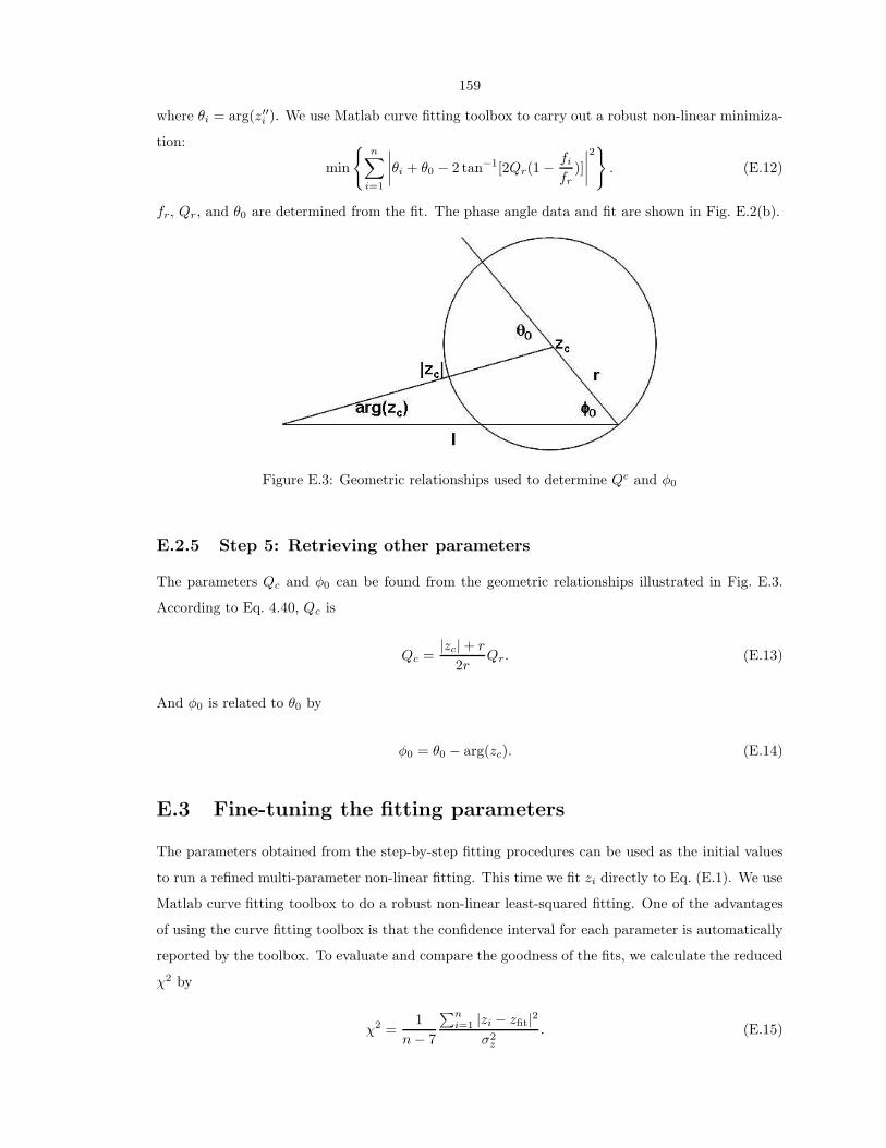
159
where θi = arg(z′′i ). We use Matlab curve fitting toolbox to carry out a robust non-linear minimiza-
tion:
min
n∑
i=1
∣∣∣∣θi + θ0 − 2 tan−1[2Qr(1 − fi
fr)]
∣∣∣∣2. (E.12)
fr, Qr, and θ0 are determined from the fit. The phase angle data and fit are shown in Fig. E.2(b).
Figure E.3: Geometric relationships used to determine Qc and φ0
E.2.5 Step 5: Retrieving other parameters
The parameters Qc and φ0 can be found from the geometric relationships illustrated in Fig. E.3.
According to Eq. 4.40, Qc is
Qc =|zc| + r
2rQr. (E.13)
And φ0 is related to θ0 by
φ0 = θ0 − arg(zc). (E.14)
E.3 Fine-tuning the fitting parameters
The parameters obtained from the step-by-step fitting procedures can be used as the initial values
to run a refined multi-parameter non-linear fitting. This time we fit zi directly to Eq. (E.1). We use
Matlab curve fitting toolbox to do a robust non-linear least-squared fitting. One of the advantages
of using the curve fitting toolbox is that the confidence interval for each parameter is automatically
reported by the toolbox. To evaluate and compare the goodness of the fits, we calculate the reduced
χ2 by
χ2 =1
n− 7
∑ni=1 |zi − zfit|2
σ2z
. (E.15)

160
1
2
3
4
5
30
210
60
240
90
270
120
300
150
330
180 0
data
fit
(a)
5.776 5.778 5.78 5.782 5.784 5.786 5.788-0.06
-0.05
-0.04
-0.03
-0.02
-0.01
0
0.01
0.02
0.03
2=2.5985
f [GHz]
z-z
fit
Re
Im
(b)
1
2
3
4
5
30
210
60
240
90
270
120
300
150
330
180 0
data
fit
(c)
5.776 5.778 5.78 5.782 5.784 5.786 5.788-0.04
-0.03
-0.02
-0.01
0
0.01
0.02
0.03
0.04
2=1.0124
f [GHz]
z-z
fit
Re
Im
(d)
Figure E.4: Refining the fitting result from the step-by-step fitting procedures. The result from thestep-by-step fitting procedures is plotted in (a) and (b), while the result from the refined fittingprocedure is plotted in (c) and (d). Data z (blue) and its fit zfit(red) are plotted in (a) and (c). Real(blue) and imaginary (green) part of the residues (zfit − z) are plotted in (b) and (d).
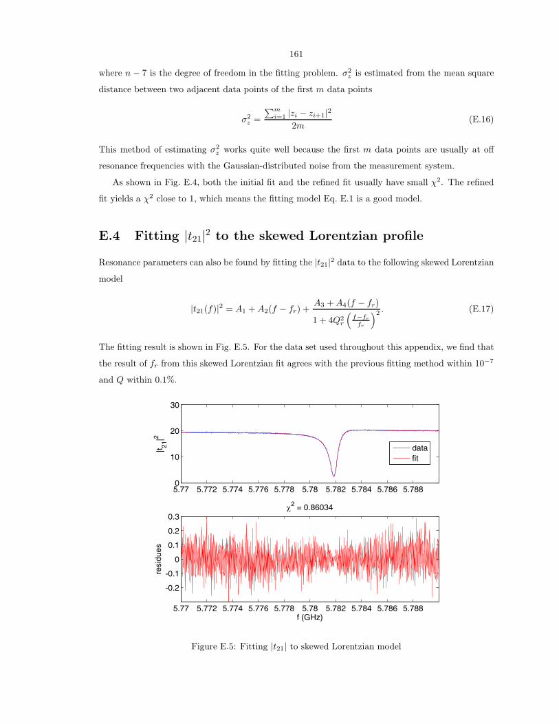
161
where n − 7 is the degree of freedom in the fitting problem. σ2z is estimated from the mean square
distance between two adjacent data points of the first m data points
σ2z =
∑mi=1 |zi − zi+1|2
2m(E.16)
This method of estimating σ2z works quite well because the first m data points are usually at off
resonance frequencies with the Gaussian-distributed noise from the measurement system.
As shown in Fig. E.4, both the initial fit and the refined fit usually have small χ2. The refined
fit yields a χ2 close to 1, which means the fitting model Eq. E.1 is a good model.
E.4 Fitting |t21|2 to the skewed Lorentzian profile
Resonance parameters can also be found by fitting the |t21|2 data to the following skewed Lorentzian
model
|t21(f)|2 = A1 +A2(f − fr) +A3 +A4(f − fr)
1 + 4Q2r
(f−fr
fr
)2 . (E.17)
The fitting result is shown in Fig. E.5. For the data set used throughout this appendix, we find that
the result of fr from this skewed Lorentzian fit agrees with the previous fitting method within 10−7
and Q within 0.1%.
5.77 5.772 5.774 5.776 5.778 5.78 5.782 5.784 5.786 5.7880
10
20
30
|t2
1|2
5.77 5.772 5.774 5.776 5.778 5.78 5.782 5.784 5.786 5.788
-0.2
-0.1
0
0.1
0.2
0.3
2 = 0.86034
f (GHz)
resid
ue
s
data
fit
Figure E.5: Fitting |t21| to skewed Lorentzian model

162
Appendix F
Calibration of IQ-mixer and datacorrection
Assume that the LO port of the IQ mixer is fed with a microwave signal of complex amplitude
ALO = 1 and the RF port with ARF = reiθ . The output voltages can be written as
I = I0 +AI cos θ (F.1)
Q = Q0 +AQ cos(θ + γ). (F.2)
Here γ is the phase difference between the I and Q channels. I0, Q0 account for the DC offset and
AI , AQ account for the unbalanced gains in the two channels. For an ideal IQ-mixer, γ = −π/2,
I0 = Q0 = 0, AI = AQ = A, and as θ goes from 0 to 2π, the IQ output traces out a circle centered
at the origin in the IQ plane. For a nonideal IQ-mixer, the output traces out an ellipse which is off
the origin, as shown in Fig. F.1. Easy to see that the center of the ellipse is at (I0, Q0). It can
be shown that the other 3 mixer parameters AI , AQ, and γ are related to the half long axis a, half
short axes b, and the orientation angle Φ by
AI =√a2 cos2 Φ + b2 sin2 Φ
AQ =√a2 sin2 Φ + b2 cos2 Φ
γ = α1 − α2
α1 = arctanb sin Φ
a cosΦ
α2 = π − arctanb cosΦ
a sin Φ. (F.3)
These relationships are illustrated in Fig. F.2 by two triangles.
According to Eq. F.3, the 3 parameters AI , AQ, and γ, which characterize a non-ideal IQ mixer,
can be fully determined from the IQ ellipses. This provides us a way to experimentally measure
these parameters. One can use a phase shifter to produce a θ sweep and obtain the IQ ellipse.

163
I
2AI
b
a
2AQ
Q
O
Figure F.1: IQ mixer output tracing out an ellipse
Unfortunately, we do not have a programmable phase shifter. Instead, we obtain the IQ ellipse by
beating two synthesizers. The output frequencies of the two synthesizers are set to be 1 kHz apart
and the IQ ellipses are digitized at a sample rate of 2 kHz for 1 second (two circles are recorded).
The data is then fit to a ellipse by standard routines to give a, b, and Φ.
The IQ ellipses measured at a number of frequencies and RF input powers by beating two
synthesizers are plotted in Fig. F.3. The ratio of AI/AQ and γ are indicated in these plots. As
expected, the AI/AQ is close to but not exactly 1. γ varies between −85 and −113 at frequencies
between 2 GHz and 10 GHz. The ellipses under different RF input powers at the same frequency
are concentric and the long and short axes scale linearly with RF amplitude. From these ellipses,
we obtain AI , AQ, and γ at discrete frequencies and powers from Eq. F.3. These values are then
interpolated at arbitrary frequency and power in the measurement range to generate the continuous
functions AI(f, PRF), AI(f, PRF), and γ(f, PRF). Using these functions, the amplitude and phase

164
1
I
(a)
2
AQ
a sin!
b cos!
x
(b)
Figure F.2: Relationships between AI , AQ, γ and a, b, Φ illustrated in two triangles
of the original RF input microwave signal can be recovered by
g =cos(θ + γ)
cos θ=AIQ
AQI
θ =
arctan cos γ−g
sin γ (I > 0)
arctan cos γ−gsin γ + π (I < 0)
r =
IAI cos θ (if cos θ 6= 0)
QAQ cos(θ+γ) (if cos θ = 0)
. (F.4)

165
−5000 0 5000 10000 15000−1
−0.5
0
0.5
1
1.5
x 104
I
Q
f=2 GHz; AI/A
Q=0.89; γ=84.8o
(a)
−4000 −2000 0 2000 4000 6000
−6000
−4000
−2000
0
2000
4000
6000
I
Q
f=3 GHz; AI/A
Q=0.99; γ=−86o
(b)
−8000−6000−4000−2000 0 2000 4000 6000
−10000
−8000
−6000
−4000
−2000
0
2000
4000
6000
I
Q
f=4 GHz; AI/A
Q=0.93; γ=−84.2o
(c)
−8000 −6000 −4000 −2000 0 2000 4000 6000−10000
−5000
0
5000
I
Q
f=5 GHz; AI/A
Q=1; γ=−82.7o
(d)
−10000 −8000 −6000 −4000 −2000 0 2000
−2000
0
2000
4000
6000
8000
10000
I
Q
f=6 GHz; AI/A
Q=1; γ=−87.9o
(e)
−10000 −5000 0 5000
−16000
−14000
−12000
−10000
−8000
−6000
−4000
−2000
0
2000
I
Q
f=7 GHz; AI/A
Q=0.95; γ=−83o
(f)
−6000 −4000 −2000 0 2000 4000 6000 8000−12000
−10000
−8000
−6000
−4000
−2000
0
2000
I
Q
f=8 GHz; AI/A
Q=0.96; γ=−91.7o
(g)
−6000 −4000 −2000 0 2000 4000−8000
−6000
−4000
−2000
0
2000
I
Q
f=9 GHz; AI/A
Q=0.92; γ=−113o
(h)
−2000 0 2000 4000 6000
−1000
0
1000
2000
3000
4000
5000
6000
7000
8000
I
Q
f=10 GHz; AI/A
Q=0.87; γ=−102o
(i)
Figure F.3: IQ ellipses from beating two synthesizers. Data and fits are plotted in blue and red,respectively. Ellipses for each frequency are measured with LO power of 13 dBm and RF power insteps of 2 dBm.

166
Appendix G
Several integrals encountered inthe calculation of ǫTLS(ω)
G.1 Integrating
χ res (ω) over TLS parameter space
Here we evaluate the integral of Eq. 5.55. Let
χ(ωε, ω) =1
~(ωε − ω + jT−12 )
+1
~(ωε + ω − jT−12 )
. (G.1)
The full integral reads
ǫTLS(ω) =
∫∫ [e·
χ res (ω) · e] P
∆0d∆0d∆dd
=
∫ ∆max
0
d∆
∫ ∆0,max
∆0,min
P
∆0d∆0
∫ π2
0
sin θdθ
×(
∆0
ε
)2
d20 cos2 θ tanh
( ε
2kT
) [ 1 + (ωε − ω)2T 22
1 + Ω2T1T2 + (ωε − ω)2T 22
]χ(ωε, ω)
. (G.2)
Let u = ∆0/ε. By applying the following change of variables
∫ ∆max
0
∫ ∆0,max
∆0,min
P
∆0d∆0d∆ −→
∫ εmax
0
∫ 1
umin
P
u√
1 − u2dudε (G.3)
the integral reduces to
ǫTLS(ω) = Pd20
∫ εmax
0
dε
∫ 1
umin
u√1 − u2
du
∫ π2
0
cos2 θ sin θdθ
×
tanh( ε
2kT
) [ 1 + (ωε − ω)2T 22
1 + Ω2T1T2 + (ωε − ω)2T 22
]χ(ωε, ω)
. (G.4)
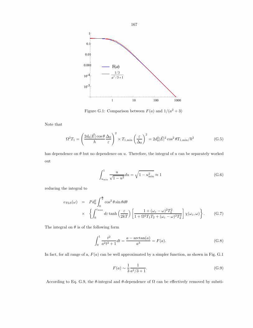
167
1 10 100 1000
10 5
10 4
0.001
0.01
0.1
1
13/
3/12
a
)(F a
Figure G.1: Comparison between F (a) and 1/(a2 + 3)
Note that
Ω2T1 =
(2d0| ~E| cos θ
~
∆0
ε
)2
× T1,min
(ε
∆0
)2
= 2d20| ~E|2 cos2 θT1,min/~
2 (G.5)
has dependence on θ but no dependence on u. Therefore, the integral of u can be separately worked
out
∫ 1
umin
u√1 − u2
du =√
1 − u2min ≈ 1 (G.6)
reducing the integral to
ǫTLS(ω) = Pd20
∫ π2
0
cos2 θ sin θdθ
×∫ εmax
0
dε tanh( ε
2kT
) [ 1 + (ωε − ω)2T 22
1 + Ω2T1T2 + (ωε − ω)2T 22
]χ(ωε, ω)
. (G.7)
The integral on θ is of the following form
∫ 1
0
t2
a2t2 + 1dt =
a− arctan(a)
a3= F (a). (G.8)
In fact, for all range of a, F (a) can be well approximated by a simpler function, as shown in Fig. G.1
F (a) ∼ 1
3
1
a2/3 + 1. (G.9)
According to Eq. G.9, the θ-integral and θ-dependence of Ω can be effectively removed by substi-
168
tuting d0/√
3 for d0 in the ε integral
ǫTLS(ω) =Pd2
0
3
∫ εmax
0
dε tanh( ε
2kT
)[ 1 + (ωε − ω)2T 22
1 + Ω2T1T2 + (ωε − ω)2T 2
2
]χ(ωε, ω) (G.10)
where the effective Rabi frequency is modified to
Ω =2d0| ~E|√
3
∆0
ε. (G.11)
G.2 ǫTLS(ω) for weak field (| ~E| → 0).
If the electric field is weak and Ω2T1T2 ≪ 1 is satisfied, we can set Ω = 0 in Eq. G.7. The integral
of θ can now be separated to yield 1/3. The integral simplifies to
ǫTLS(ω) =Pd2
0
3~
∫ εmax
0
tanh( ε
2kT
)[ 1
ωε − ω + jT−12
+1
ωε + ω − jT−12
]dε. (G.12)
Now let x = ε/kT , z = (~ω − j~T−12 )/kT and xm = εmax/kT . We rewrite the integral as
ǫTLS(ω) =Pd2
0
3
∫ xm
0
tanh(x
2)
2x
x2 − z2dx. (G.13)
The following are pure mathematical derivations
∫ xm
0
tanh(x
2)
2x
x2 − z2dx
=
∫ xm
0
[tanh(
x
2) − 1
] 2x
x2 − z2dx+
∫ xm
0
2x
x2 − z2dx
≈∫ ∞
0
−2
ex + 1
2x
x2 − z2dx+ log(
−x2m
z2)
= −2
∫ ∞
0
(1
ex − 1− 2
e2x − 1
)2x
x2 − z2dx+ log(
−x2m
z2)
= −2
[∫ ∞
0
1
ex − 1
2x
x2 − z2dx−
∫ ∞
0
2
e2x − 1
2x
x2 − z2dx− log(
jxm
z)
]
= −2
[∫ ∞
0
1
e2πt − 1
2t
t2 + (jz/2π)2dt−
∫ ∞
0
2
e2πt − 1
2t
t2 − (jz/π)2dt− log(
jxm
z)
]
= −2
[∫ ∞
0
1
e2πt − 1
2t
t2 + ( −z2πj )2
dt−∫ ∞
0
2
e2πt − 1
2t
t2 + (−2z2πj )2
dt− log(jxm
z)
]
= −2
[log(
−z2πj
) +2πj
2z− ψ(
−z2πj
)
]− 2
[log(
−zπj
) +πj
2z− ψ(
−zπj
)
]− log(
jxm
z)
= −2
[ψ(
1
2− z
2πj) − log(
xm
2π)
]. (G.14)

169
In the derivations above, we have applied the following two formula found in Abramowitz and Stegun
(page 259)[52], to express the integral in terms of complex digamma function ψ:
ψ(z) = log z − 1
2z− 2
∫ ∞
0
tdt
(t2 + z2)(e2πt − 1)
ψ(2z) =1
2ψ(z) +
1
2ψ(z +
1
z) + log 2. (G.15)
Therefore in the weak field limit,
ǫTLS(ω) = −2Pd20
3
[ψ(
1
2− ~ω − jT−1
2
2πjkT) − log(
εmax
2πkT)
]. (G.16)
G.3 ǫTLS(ω) for nonzero ~E field.
For general nonzero electrical field, we evaluate the real part (ǫ′TLS) and the imaginary part (ǫ′′TLS)
separately.
For the integral of ǫ′′TLS, the major contribution is from the first term in χ(ωε, ω) and the second
term can be neglected. After dropping the second term, the integral becomes
ǫ′′TLS(ω) =Pd2
0
3~
∫ εmax
0
dε tanh( ε
2kT
)
−T−12
(T−12
√1 + Ω
2T1T2)2 + (ωε − ω)2
. (G.17)
The factor in the square brackets is a Lorentzian centered at ωε with a line width of T−12
√1 + Ω
2T1T2.
Because within the width of the Lorentizian tanh(ε/2kT ) is almost constant, it can be taken out of
the integral leading to
ǫ′′TLS(ω) ≈ −Pd20
3~tanh
(~ω
2kT
)∫ εmax
0
dε
−T−12
(T−12
√1 + Ω
2T1T2)2 + (ωε − ω)2
≈ −πPd20
3
tanh(
~ω2kT
)√
1 + Ω2T1T2
. (G.18)
The field-dependent loss tangent is given by
δTLS = δ0tanh
(~ω2kT
)√
1 + (| ~E|/Ec)2(G.19)
where the critical electric field is
Ec =
√3~
2d0| ~E|√T1,minT2
. (G.20)

170
Next, we work on the real part of the integral in Eq. G.7 for ǫ′TLS(ω). Let κ(| ~E|) =
√1 + Ω
2T1T2
be the saturation factor. The difference in ǫ′TLS(ω) between strong field and zero field is calculated
by
δǫ′(κ) = ǫ′TLS(κ) − ǫ′TLS(0)
=Pd2
0
3~
∫ εmax
0
tanh( ε
2kT
)[ 1 + (ωε − ω)2T 22
1 + Ω2T1T2 + (ωε − ω)2T 2
2
− 1
]
×
(ωε − ω)
(ωε − ω)2 + (T−12 )2
+(ωε + ω)
(ωε + ω)2 + (T−12 )2
dε. (G.21)
Now we calculate the contribution from the two terms in the curly brackets separately.
δǫ′1 =Pd2
0
3~
∫ εmax
0
tanh( ε
2kT
)[ 1 + (ωε − ω)2T 22
1 + Ω2T1T2 + (ωε − ω)2T 2
2
− 1
]ωε − ω
(ωε − ω)2 + (T−12 )2
dε
=Pd2
0
3~
∫ εmax
0
tanh( ε
2kT
)[ ∆ω
∆ω2 + (κT−12 )2
− ∆ω
∆ω2 + (T−12 )2
]dε. (G.22)
Because the term in the square brackets
∆ω
∆ω2 + (κT−12 )2
− ∆ω
∆ω2 + (T−12 )2
=(1 − κ2)(T−1
2 )2∆ω
[∆ω2 + (T−12 )2][∆ω2 + (κT−1
2 )2](G.23)
is an odd function of ∆ω which has significant contribution to the integral only when |ωε−ω| . κT−12 ,
we can replace tanh(
ε2kT
)by its Taylor expansion at ε = ~ω and extend the integral limits to ±∞,
δǫ′1 ≈ Pd20
3
∫ ∞
−∞
[tanh
(~ω
2kT
)+ sech2
(~ω
2kT
)~∆ω
2kT
] [∆ω
∆ω2 + (κT−12 )2
− ∆ω
∆ω2 + (T−12 )2
]d∆ω
=πPd2
0
3sech2
(~ω
2kT
)~T−1
2
2kT(1 − κ)
(G.24)
The contribution from the second term in the curly brackets is Eq. G.21.
δǫ′2 =Pd2
0
3~
∫ εmax
0
tanh( ε
2kT
)[ −Ω2T1T2
1 + Ω2T1T2 + (ωε − ω)2T 2
2
]ωε + ω
(ωε + ω)2 + (T−12 )2
dε
(G.25)
where the term in the square brackets is only nonzero within a small range around ωε ∼ ω in which

171
1 2 3 4 5
3.0
2.5
2.0
1.5
1.0
0.5
1 2 3 4 5
0.30
0.25
0.20
0.15
0.10
0.05
!"# TLS'
!0'TLS#
'$#
1'$#
2'$#
Numerical
Analytical
% T %
T
Figure G.2: δǫ′, δǫ′1 and δǫ′2 as a function of temperature. Left panel shows ǫ′TLS for zero field κ = 0(blue) and nonzero field κ = 3 (red). Their difference is plotted by the bottom curve in the rightpanel, as well as the two contributions δǫ′1 and δǫ′2. In the right panel, solid lines are calculatedfrom evaluating the exact integrals numerically while the dashed line are calculated from the derivedapproximate formula.
all other terms are almost constant. Therefore
δǫ′2 ≈ Pd20
3~tanh
(~ω
2kT
)1
2ω
∫ ∞
−∞
[−Ω
2T1T2
1 + Ω2T1T2 + (ωε − ω)2T 2
2
]dε
=πPd2
0
3tanh
(~ω
2kT
)T−1
2
2ω
1 − κ2
κ
(G.26)
Finally, we have derived
ǫ′TLS(κ) − ǫ′TLS(0)
= δǫ′1 + δǫ′2
=πPd2
0
3
[sech2
(~ω
2kT
)~T−1
2
2kT(1 − κ) + tanh
(~ω
2kT
)T−1
2
2ω
1 − κ2
κ
](G.27)
The temperature variation of ǫ′TLS for zero field κ = 0 and nonzero field κ = 3 are plotted in
the left panel in Fig. G.2. We can see that ǫ′TLS decreases with the field strength. The difference
between the two curves δǫ′ = ǫTLS(κ = 3) − ǫTLS(κ = 0), separated into the two contributions
δǫ′1 and δǫ′2, evaluated both numerically from the exact integrals and analytically from the derived
approximate formula, are plotted in the right panel of Fig. G.2. There we see that the approximate
formula works pretty well.

172
Appendix H
Semi-empirical frequency noiseformula for a transmission lineresonator
In this appendix, we derive the formula of frequency noise in the high power regime for a transmission
line resonator from the semi-empirical noise model Eq. 5.80
Sδfr (ν)
f2r
= κ(ν, ω, T )
∫Vh
| ~E|3d3r
4(∫
V ǫ| ~E|2d3r)2 (H.1)
We consider a m-wave transmission line resonator in general. For example, for a quarter-wave
resonator m = 1/4 and for a half-wave resonator m = 1/2. Assume that the transmission line goes
in the z-direction with z = 0 and z = l represents the coupler end (always an open end) and the
opposite end, respectively. The cross-section of the transmission line is in the x−y plane, with x-axis
parallel to surface of the metal film and y-axis perpendicular to the surface. The spatial distribution
of the electric field in the resonator has a standing wave pattern given by
|E(x, y, z)| = V0ρ(x, y)| cos(2πmz
l)| (H.2)
where V0 is the voltage at z=0 (a harmonic time dependence of ejωt is assumed and omitted as
usual), which is related to the internal power Pint and readout power Pµw by,
Pint =V 2
+
2Zr=
(V0/2)2
2Zr=
1
2πmPµw
Q2
Qc(H.3)
V0 =
√4Zr
πm
Q2r
QcPµw (H.4)
ρ(x, y) is the field distribution in the cross-sectional plane normalized by V0. The denominator in
Eq. H.1 is related to the electric energy in the system and can be expressed in terms of transmission

173
line parameters
2
∫
V
ǫE(~r)2d~r = CV 20 l (H.5)
Inserting Eq. H.2 and Eq. H.5 to Eq. H.1 yields
Sδfr (ν)
f2r
= κ(ν, ω, T )4∫Ahρ(x, y)3dxdy
3πC2V0l(H.6)
Because of the term V0 in the denominator, Eq. H.6 gives the correct P−1/2int power dependence
of noise. Eq. H.6 also predict that the noise scales inversely with length, which arises from the
incoherent sum of the contribution from independent fluctuators along the z-axis.
The most important part of the noise formula Eq. H.6 is the following integral
I3 =
∫
Ah
ρ(x, y)3dxdy (H.7)
which is taken in the area Ah occupied by the TLS host material in the cross-sectional plane. It can
be shown that for microstrip transmission line
I3 =
∫
Ah
ρ(x, y)3dxdy ≈ w
h2(H.8)
where the field is approximated by that of a parallel plate capacitor. Here w and h are the width
and the thickness of the dielectric in the microstrip. For a surface distribution of TLS,
I3 =
∫
Ah
ρ(x, y)3dxdy ≈ t
∫
Ch
ρ(ξ)3dξ (H.9)
where the contour Ch runs over the TLS distributed surface and t is the thickness of the TLS layer.

174
Bibliography
[1] P. de Bernardis, P. A. R. Ade, J. J. Bock, J. R. Bond, J. Borrill, A. Boscaleri, K. Coble, B. P.
Crill, G. De Gasperis, P. C. Farese, P. G. Ferreira, K. Ganga, M. Giacometti, E. Hivon, V. V.
Hristov, A. Iacoangeli, A. H. Jaffe, A. E. Lange, L. Martinis, S. Masi, P. V. Mason, P. D.
Mauskopf, A. Melchiorri, L. Miglio, T. Montroy, C. B. Netterfield, E. Pascale, F. Piacentini,
D. Pogosyan, S. Prunet, S. Rao, G. Romeo, J. E. Ruhl, F. Scaramuzzi, D. Sforna, and
N. Vittorio, “A flat universe from high-resolution maps of the cosmic microwave background
radiation,” Nature 404 (2000), no. 6781, 955–959.
[2] A. E. Lange, P. A. R. Ade, J. J. Bock, J. R. Bond, J. Borrill, A. Boscaleri, K. Coble, B. P.
Crill, P. de Bernardis, P. Farese, P. Ferreira, K. Ganga, M. Giacometti, E. Hivon, V. V.
Hristov, A. Iacoangeli, A. H. Jaffe, L. Martinis, S. Masi, P. D. Mauskopf, A. Melchiorri,
T. Montroy, C. B. Netterfield, E. Pascale, F. Piacentini, D. Pogosyan, and S. Prunet,
“Cosmological parameters from the first results of boomerang,” Physical Review D 63 (2001),
no. 4, 042001.
[3] F. Simon, “Application of low temperature calorimetry to radioactive measurements,” Nature
135 (1935) 763.
[4] F. J. Low, “Low-temperature geranium bolometer,” Journal of the Optical Society of America
A 51 (1961), no. 11, 1300.
[5] J. Glenn, J. J. Bock, G. Chattopadhyay, S. F. Edgington, A. E. Lange, J. Zmuidzinas, P. D.
Mauskopf, B. Rownd, L. Yuen, and P. A. R. Ade, “Bolocam: a millimeter-wave bolometric
camera,” in Proceedings SPIE–the International Society of Optical Engineering, T. G. Phillips,
ed., vol. 3357, pp. 326–334. 1998.
[6] K. D. Irwin, G. C. Hilton, D. A. Wollman, and J. M. Martinis, “X-ray detection using a
superconducting transition-edge sensor microcalorimeter with electrothermal feedback,”
Applied Physics Letters 69 (1996), no. 13, 1945–1947.
[7] K. D. Irwin and G. C. Hilton, “Cryogenic particle detection,” in Topics in Applied Physics,
C. Enss, ed., vol. 99, pp. 63–149. Springer, Berlin, Germany, 2005.

175
[8] B. Cabrera, R. M. Clarke, P. Colling, A. J. Miller, S. Nam, and R. W. Romani, “Detection of
single infrared, optical, and ultraviolet photons using superconducting transition edge
sensors,” Applied Physics Letters 73 (1998), no. 6, 735–737.
[9] K. D. Irwin, G. C. Hilton, J. M. Martinis, S. Deiker, N. Bergren, S. W. Nam, D. A. Rudman,
and D. A. Wollman, “A mo-cu superconducting transition-edge microcalorimeter with 4.5 ev
energy resolution at 6 kev,” Nuclear Instruments and Methods in Physics Research Section A:
Accelerators, Spectrometers, Detectors and Associated Equipment 444 (2000) 184–187.
[10] S. F. Lee, J. M. Gildemeister, W. Holmes, A. T. Lee, and P. L. Richards, “Voltage-biased
superconducting transition-edge bolometer with strong electrothermal feedback operated at
370 mk,” Applied Optics 37 (1998), no. 16, 3391–3397.
[11] A. Fleischmann, C. Enss, and G. M. Seidel, “Cryogenic particle detection,” in Topics in
Applied Physics, C. Enss, ed., vol. 99, pp. 151–216. Springer, Berlin, Germany, 2005.
[12] D. Twerenbold, “Giaever-type superconducting tunneling junctions as high-resolution
X-ray-detectors,” Europhysics Letters 1 (1986), no. 5, 209–214.
[13] A. Peacock, P. Verhoeve, N. Rando, A. vanDordrecht, B. Taylor, C. Erd, M. Perryman,
R. Venn, J. Howlett, D. Goldie, J. Lumley, and M. Wallis, “Single optical photon detection
with a superconducting tunnel junction,” Nature 381 (1996), no. 6578, 135–137.
[14] P. K. Day, H. G. LeDuc, B. A. Mazin, A. Vayonakis, and J. Zmuidzinas, “A broadband
superconducting detector suitable for use in large arrays,” Nature 425 (2003), no. 6960,
817–821.
[15] B. A. Mazin, P. K. Day, J. Zmuidzinas, and H. G. LeDuc, “Multiplexable kinetic inductance
detectors,” AIP Conference Proceedings 605 (2002) 309–312.
[16] B. A. Mazin, Microwave kinetic inductance detectors. PhD thesis, Caltech, 2004.
[17] J. Baselmans, S. J. C. Yates, R. Barends, Y. J. Y. Lankwarden, J. R. Gao, H. Hoevers, and
T. M. Klapwijk, “Noise and sensitivity of aluminum kinetic inductance detectors for sub-mm
astronomy,” Journal of Low Temperature Physics 151 (2008) 524–529.
[18] G. Vardulakis, S. Withington, D. J. Goldie, and D. M. Glowacka, “Superconducting kinetic
inductance detectors for astrophysics,” Measurement Science and Technology 19 (2008), no. 1,
015509.
[19] M. Tinkham, Introduction to Superconductivity, 2nd ed. McGraw-Hill, New York, 1996.

176
[20] B. A. Mazin, B. Bumble, P. K. Day, M. E. Eckart, S. Golwala, J. Zmuidzinas, and F. A.
Harrison, “Position sensitive X-ray spectrophotometer using microwave kinetic inductance
detectors,” Applied Physics Letters 89 (2006), no. 22, 222507.
[21] P. K. Day, H. G. Leduc, A. Goldin, T. Vayonakis, B. A. Mazin, S. Kumar, J. Gao, and
J. Zmuidzinas, “Antenna-coupled microwave kinetic inductance detectors,” Nuclear
Instruments and Methods in Physics Research Section A: Accelerators, Spectrometers,
Detectors and Associated Equipment 559 (2006) 561–563.
[22] J. Schlaerth, A. Vayonakis, P. Day, J. Glenn, J. Gao, S. Golwala, S. Kumar, H. LeDuc,
B. Mazin, J. Vaillancourt, and J. Zmuidzinas, “A millimeter and submillimeter kinetic
inductance detector camera,” Journal of Low Temperature Physics 151 (2008) 684–689.
[23] B. A. Mazin, M. E. Eckart, B. Bumble, S. Golwala, P. K. Day, J. Gao, and J. Zmuidzinas,
“Optical/UV and X-ray microwave kinetic inductance strip detectors,” Journal of Low
Temperature Physics 151 (2008) 537–543.
[24] B. A. Mazin, P. K. Day, K. D. Irwin, C. D. Reintsema, and J. Zmuidzinas, “Digital readouts
for large microwave low-temperature detector arrays,” Nuclear Instruments and Methods in
Physics Research Section A: Accelerators, Spectrometers, Detectors and Associated Equipment
559 (2006) 799–801.
[25] S. Golwala, J. Gao, D. Moore, B. Mazin, M. Eckart, B. Bumble, P. Day, H. G. LeDuc, and
J. Zmuidzinas, “A wimp dark matter detector using mkids,” Journal of Low Temperature
Physics 151 (2008) 550–556.
[26] M. Daal, B. Sadoulet, and J. Gao, “Kinetic inductance phonon sensors for the cryogenic dark
matter search experiment,” Journal of Low Temperature Physics 151 (2008) 544–549.
[27] K. W. Lehnert, K. D. Irwin, M. A. Castellanos-Beltran, J. A. B. Mates, and L. R. Vale,
“Evaluation of a microwave SQUID multiplexer prototype,” IEEE Transactions on Applied
Superconductivity 17 (2007), no. 2, 705–709.
[28] J. A. B. Mates, G. C. Hilton, K. D. Irwin, L. R. Vale, and K. W. Lehnert, “Demonstration of
a multiplexer of dissipationless superconducting quantum interference devices,” Applied
Physics Letters 92 (2008), no. 2, 023514.
[29] I. Hahn, B. Bumble, H. Leduc, M. Weilert, and P. Day, “An X-band squid multiplexer,” AIP
Conference Proceedings 850 (2006) 1613–1614.
[30] I. Hahn, P. K. Day, B. Bumble, and H. G. Leduc, “Recent results of a new microwave SQUID
multiplexer,” Journal of Low Temperature Physics 151 (2008) 934–939.

177
[31] A. Wallraff, D. I. Schuster, A. Blais, L. Frunzio, R.-S. Huang, J. Majer, S. Kumar, S. M.
Girvin, and R. J. Schoelkopf, “Strong coupling of a single photon to a superconducting qubit
using circuit quantum electrodynamics,” Nature 431 (2004), no. 7005, 162–167.
[32] E. Jaynes and F. Cummings, “Comparison of quantum and semiclassical radiation theories
with application to the beam maser,” Proceedings of IEEE 51 (1963), no. 1, 89–109.
[33] J. Majer, J. M. Chow, J. M. Gambetta, J. Koch, B. R. Johnson, J. A. Schreier, L. Frunzio,
D. I. Schuster, A. A. Houck, A. Wallraff, A. Blais, M. H. Devoret, S. M. Girvin, and R. J.
Schoelkopf, “Coupling superconducting qubits via a cavity bus,” Nature 449 (2007) 443.
[34] A. A. Houck, D. I. Schuster, J. M. Gambetta, J. A. Schreier, B. R. Johnson, J. M. Chow,
L. Frunzio, J. Majer, M. H. Devoret, S. M. Girvin, and R. J. Schoelkopf, “Generating single
microwave photons in a circuit,” Nature 449 (2007) 328.
[35] D. I. Schuster, A. A. Houck, J. A. Schreier, A. Wallraff, J. M. Gambetta, A. Blais, L. Frunzio,
J. Majer, B. R. Johnson, M. H. Devoret, S. M. Girvin, and R. J. Schoelkopf, “Resolving
photon number states in a superconducting circuit,” Nature 445 (2007) 515.
[36] C. A. Regal, J. D. Teufel, and K. W. Lehnert, “Measuring nanomechanical motion with a
microwave cavity interferometer,” Nature Physics advanced online publication (2008).
[37] R. G. Chambers, “The anomalous skin effect,” Proceedings of the Royal Society of London.
Series A, Mathematical and Physical Sciences 215 (1952), no. 1123, 481–497.
[38] F. London, “Electrodynamics of macroscopic fields in supraconductors,” Nature 137 (1936),
no. 3476, 991–992.
[39] D. C. Mattis and J. Bardeen, “Theory of the anomalous skin effect in normal and
superconducting metals,” Physical Review 111 (1958), no. 2, 412–417.
[40] R. Popel, “Electromagnetic properties of superconductors,” in Superconducting Quantum
Electronics, V. Kose, ed., ch. 3, pp. 44–78. Springer-Verlag, Berlin, Germany, 1989.
[41] A. B. Pippard, “An experimental and theoretical study of the relation between magnetic field
and current in a superconductor,” Proceedings of the Royal Society of London. Series A,
Mathematical and Physical Sciences 216 (1953), no. 1127, 547–568.
[42] J. Bardeen, L. N. Cooper, and J. R. Schrieffer, “Microscopic theory of superconductivity,”
Physical Review 106 (1957), no. 1, 162–164.
[43] G. E. H. Reuter and E. H. Sondheimer, “The theory of the anomalous skin effect in metals,”
Proceedings of the Royal Society of London. Series A, Mathematical and Physical Sciences
195 (1948), no. 1042, 336–364.

178
[44] J. R. Hook, “A method for calculating the microwave surface impedance of superconducting
films,” Journal of Low Temperature Physics 23 (1976), no. 5, 645–661.
[45] J. Ward, F. Rice, G. Chattopadhyay, and J. Zmuidzinas, “Supermix: A flexible software
library for high-frequency circuit simulation, including sis mixers and superconducting
elements,” in Proceedings SPIE–the International Society of Optical Engineering, pp. 269–281.
1999.
[46] B. Mhlschlegel, “Die thermodynamischen funktionen des supraleiters,” Zeitschrift fr Physik A
Hadrons and Nuclei 155 (1959) 313–327.
[47] S. Sridhar, “Microwave response of thin-film superconductors,” Journal of Applied Physics 63
(1988), no. 1, 159–166.
[48] R. E. Glover and M. Tinkham, “Conductivity of superconducting films for photon energies
between 0.3 and 4ktc,” Physical Review 108 (1957), no. 2, 243–256.
[49] C. S. Owen and D. J. Scalapino, “Superconducting state under the influence of external
dynamic pair breaking,” Physical Review Letters 28 (1972), no. 24, 1559–1561.
[50] J. Gao, J. Zmuidzinas, A. Vayonakis, P. K. Day, B. A. Mazin, and H. G. Leduc, “Equivalence
of the effects on the complex conductivity of superconductor due to temperature change and
external pair breaking,” Journal of Low Temperature Physics 151 (2008) 557–563.
[51] C. P. Wen, “Coplanar waveguide: A surface strip transmission line suitable for nonreciprocal
gyromagnetic device applications,” IEEE Transactions on Microwave Theory and Techniques
17 (Dec 1969), no. 12, 1087–1090.
[52] M. Abramowitz and I. A. Stegun, Handbook of Mathematical Functions: with Formulas,
Graphs, and Mathematical Tables. Dover Publications, New York, 1965.
[53] http://www.math.udel.edu/ driscoll/software/SC.
[54] Matlab user manual.
[55] R. E. Collin, Foundations for Microwave Engineering, 2nd edition. IEEE Press, New York,
2000.
[56] W. H. Chang, “The inductance of a superconducting strip transmission line,” Journal of
Applied Physics 50 (1979), no. 12, 8129–8134.
[57] D. M. Pozar, Microwave Engineering, 2nd edition. John Wiley and Sons, New York, 1998.
[58] A. B. Zorin, F.-J. Ahlers, J. Niemeyer, T. Weimann, and H. Wolf, “Background charge noise in
metallic single-electron tunneling devices,” Physical Review B 53 (1996), no. 20, 13682–13687.

179
[59] J. M. Martinis, K. B. Cooper, R. McDermott, M. Steffen, M. Ansmann, K. D. Osborn,
K. Cicak, S. Oh, D. P. Pappas, R. W. Simmonds, and C. C. Yu, “Decoherence in Josephson
qubits from dielectric loss,” Physical Review Letters 95 (2005), no. 21, 210503.
[60] W. A. Phillips, “Tunneling states in amorphous solids,” Journal of Low Temperature Physics
7 (1972), no. 3-4, 351–360.
[61] P. W. Anderson, B. I. Halperin, and C. M. Varma, “Anomalous low-temperature thermal
properties of glasses and spin glasses,” Philosophical Magazine 25 (1972) 1–9.
[62] S. Kumar, P. Day, H. LeDuc, B. Mazin, M. Eckart, J. Gao, and J. Zmuidzinas, “Frequency
noise in superconducting thin–film resonators,” APS March Meeting abstract (2006).
http://meetings.aps.org/link/BAPS.2006.MAR.B38.2.
[63] S. Kumar, J. Gao, J. Zmuidzinas, B. A. Mazin, H. G. Leduc, and P. K. Day, “Temperature
dependence of the frequency and noise of superconducting coplanar waveguide resonators,”
Applied Physics Letters 92 (2008) 123503.
[64] J. Gao, J. Zmuidzinas, B. A. Mazin, P. K. Day, and H. G. Leduc, “Experimental study of the
kinetic inductance fraction of superconducting coplanar waveguide,” Nuclear Instruments and
Methods in Physics Research, Section A 559 (2006) 585–587.
[65] W. A. Phillips, “Two–level states in glasses,” Reports on Progress in Physics 50 (1987)
1657–1708.
[66] W. A. Phillips, Amorphous solids: low-temperature properties. Springer-Verlag, Berlin, and
New York, 1981.
[67] F. Bloch, “Nuclear induction,” Physical Review 70 (1946), no. 7-8, 460–474.
[68] S. Hunklinger and W. Arnold, Physical Acoustics, vol. 12, ch. 3, p. 155. Academic, New York,
1976.
[69] L. Hilico, C. Fabre, S. Reynaud, and E. Giacobino, “Linear input-output method for quantum
fluctuations in optical bistability with two-level atoms,” Physical Review A 46 (1992), no. 7,
4397–4405.
[70] J. Gao, J. Zmuidzinas, B. A. Mazin, P. K. Day, and H. G. LeDuc, “Noise properties of
superconducting coplanar waveguide microwave resonators,” Applied Physics Letters 90
(2007), no. 102507, 817–821.
[71] R. N. Simons, Coplanar Waveguide Circuits Components and Systems. John Wiley and Sons,
New York, 2001.

180
[72] J. Gao, M. Daal, A. Vayonakis, S. Kumar, J. Zmuidzinas, B. Sadoulet, B. A. Mazin, P. K.
Day, and H. G. Leduc, “Experimental evidence for a surface distribution of two-level systems
in superconducting lithographed microwave resonators,” Applied Physics Letters 92 (2008),
no. 15, 152505.
[73] J. Gao, B. Mazin, M. Daal, P. Day, H. LeDuc, and J. Zmuidzinas, “Power dependence of
phase noise in microwave kinetic inductance detectors,” in Proceedings SPIE–the International
Society of Optical Engineering, J. Zmuidzinas, W. S. Holland, S. Withington, and W. D.
Duncan, eds., vol. 6275, p. 627509. 2006.
[74] J. Gao, M. Daal, J. M. Martinis, A. Vayonakis, J. Zmuidzinas, B. Sadoulet, B. A. Mazin,
P. K. Day, and H. G. Leduc, “A semiempirical model for two-level system noise in
superconducting microresonators,” Applied Physics Letters 92 (2008), no. 21, 212504.
[75] K. Oto, S. Takaoka, K. Murase, and S. Ishida, “Superconductivity in ptsi ultrathin films,”
Journal of Applied Physics 76 (1994), no. 9, 5339–5342.
[76] K. Radermacher, D. Monroe, A. E. White, K. T. Short, and R. Jebasinski, “Quantum
transport of buried single-crystalline cosi2 layers in (111)si and (100)si substrates,” Phys. Rev.
B 48 (1993), no. 11, 8002–8015.
[77] M. C. Gaidis, Superconducting Tunnel Junctions as Single Photon X-Ray Detector. PhD
thesis, Yale University, 1994.
[78] D. L. Snyder, Random Point Processes. John Wiley and Sons, New York, 1975.
[79] N. Chernov and C. Lesort, “Least squares fitting of circles,” Journal of Mathematical Imaging
and Vision 23 (2005), no. 3, 239–252.