Embed Size (px)
Citation preview

The physical properties of grown p-i-n junctions in siliconcarbideGreebe, C.A.A.J.
DOI:10.6100/IR117420
Published: 01/01/1962
Document VersionPublisher’s PDF, also known as Version of Record (includes final page, issue and volume numbers)
Please check the document version of this publication:
• A submitted manuscript is the author's version of the article upon submission and before peer-review. There can be important differencesbetween the submitted version and the official published version of record. People interested in the research are advised to contact theauthor for the final version of the publication, or visit the DOI to the publisher's website.• The final author version and the galley proof are versions of the publication after peer review.• The final published version features the final layout of the paper including the volume, issue and page numbers.
Link to publication
Citation for published version (APA):Greebe, C. A. A. J. (1962). The physical properties of grown p-i-n junctions in silicon carbide Eindhoven:Technische Hogeschool Eindhoven DOI: 10.6100/IR117420
General rightsCopyright and moral rights for the publications made accessible in the public portal are retained by the authors and/or other copyright ownersand it is a condition of accessing publications that users recognise and abide by the legal requirements associated with these rights.
• Users may download and print one copy of any publication from the public portal for the purpose of private study or research. • You may not further distribute the material or use it for any profit-making activity or commercial gain • You may freely distribute the URL identifying the publication in the public portal ?
Take down policyIf you believe that this document breaches copyright please contact us providing details, and we will remove access to the work immediatelyand investigate your claim.
Download date: 17. Jun. 2018

THE PHYSICAL PROPERTIES OF GROWN p-i-n JUNCTIONS IN
SILICON CARBIDE
C.A. A. J. GREEBE

THE PHYSICAL PROPERTJES OF GROWN p-i-n JUNCTIONS IN
SILICON CARBIDE
PROEFSCHRIFT
TER VERKRIJGING VAN DE GRAAD VAN DOC
TOR IN DE TECHNISCHE WETENSCHAP AAN DE
TECHNISCHE HOGESCHOOL TE EINDHOVEN
OP GEZAG VAN DE RECTOR MAGNIFICUS
DR. K. POSTHUMUS, HOOGLERAAR IN DE
AFDELING DER SCHEIKUNDIGE TECHNOLOGIE,
VOOR EEN COMMISSIE UIT DE SENAAT
TE VERDEDIGEN OP VRIJDAG 29 JUNI 1962
DES NAMIDDAGS TE 14 UUR.
door
CORNELIS ALEIDUS ARNOLDUS JOHANNES GREEBE
FYSISCH DOCTORANDUS
geboren te Zaandam.

Dit proefschrift werd goedgekeurd door de promotor
prof. dr. G. Diemer.

Aan mijn schoonouders, de Heer en Mevrouw Brouwer-v.Milgen.
Aan mijn vrouw.

CONTENTS
CHAPTER 1. HISTORICAL AND THEORETICAL CONTEXT.
I. I. Iotroduction . . . . . . . 1 1.2 The preparation of SiC . . 1
I.2.1 The Acheson-Process. 1 I.2.2 The Lely Process . . 2
1.3 Genera! properties of SiC . 2 l.3. l Chemica! properties . 2 I.3.2 Crystallographic properties 2 I.3.3 SiC as a semiconductor 3
1.4 Previous work on rectifying systems in SiC. 4 1.5 Theoretica! context of the present investigation 5
1.5. l Introduction . . . . . . . . . . . . . 5 1.5.2 p-n junctions and related structures in genera! . 5 I.5.3 p-n junctions and rela ted structures in semiconductors with a high
bandgap . . . . . . . . . . . . . . . . . 8
CHAPTER Il. EXPERIMENTAL PROCEDURES 11
II.! Preparation and selection of samples . . . . . . . 11 II.1.1 Preparation of crystals containing p-n structures 11 11.1.2 Preparation and selection of samples . . . . 11
11.2 Measuring techniques . . . . . . . . . . . . . 14 11.2.1 Introduction. . . . . . . . . . . . . . . 14 11.2.2 The measurement of the dark characteristics. 14 II.2.3 The measurement of the photovoltaic effect . 16 II.2.4 The measurement of the spectra! distribution of the p-n-luminescence 18
CHAPTER III. EXPERIMENTAL RESULTS. . . . . . 21
lII. l Introduction . . . . . . . . . . . . . . . . . . . 21 III.2 Steady state current-voltage characteristics in the dark. 24
!II .2.1 The forward characteristics 24 III.2.2 The reverse characteristics . . . . . . . 28
Ill.3 The photovoltaic effect . . . . . . . . . . . 28 lII.4 The spectra! distributioo of the p-11 luminescence 31
III.4. l Forward bias 31 111.4.2 Reverse bias . . . . . . . . . . . . . 33
CHAPTER IV. THEORETICAL CONSIDERATIONS . . 34
IV.! Introduction . . . . . . . . . . . . . . . . . . . 34 IV.2 Assumptions . . . . . . . . . . . . . . . . . . . 35 IV.3 The solution of the continuity equations in the i-region 37 IV.4 The solution of the continuity equations in the p- and n-regioos . 38 IV.5 Evaluation of the boundary conditions. . . . . . . . . . . . 39 JV.6 The evaluation of the curreot J in terms of Vi + V,; the voltage drop V;
over the i-region . . . . . . . . . . . . . . . . . . . . . . . . . 40 1V.7 The dark case . . . . . . . . . . . . . . . . . . . . . . . . . . 42 IV.8 Explicit evaluation of the photovoltaic effect under the assumption that in
the i-region µ,nn and µ,pp are equal . . . 43 IV.8.1 Introduction . . . . . . . . . . . . . . . . . . . . . . . . 43 IV.8.2 Terminology . . . . . . . . . . . . . . . . . . . . . . . . 43 IV.8.3 The Equivalent Bias Photocurrent as a function of total harrier
voltage . . . . . . . . . . . . . . . . . . . . . . . . . 44 IV.8.4 The evaluation of Vi as a function of Y for Ja » qg ILn - L pf . 46 IV.8.5 The evaluation of Jas a function of Vt for constant J EBP . . • 48
IV.9 Outline of the theory for the case that µ,nn #- µ,pp in the i-region (under the simplifying assumption that Ln = L p) . . . . . . . . . . . . . 50

CHAPTER V. CONFRONTATION OF THEORY AND EXPERIMENT: THE SPECTRAL DISTRIBUTION OF THE p-n LUMINESCENCE ........ .
CHAPTER Vl. CONFRONTATION OF THEORY AND EXPERI-MENT: PHOTOVOLTAIC EFFECT AND DARK
54
CHARACTERISTICS . . . . . . . . . . . . . . 56
Vl.! Introduction . . . . . . . . . . . . . . . . . . . . . . . . . . . 56 VI.2 Qualitative interpretation of the steady state forward characteristics in
darkoess and of the photovoltaic effect . . . . . . . . . . . . . 56 VI.3 The influence of non uniform generation . . . . . . . . . . . . 57 Vl.4 Quantitative analysis of the forward characteristics and of the photo-
voltaic effect . . . . . . . . . . . . . . . . . 59 Vl.4.1 Junctions prepared froril recrystallized SiC 59
VI.4.1.1 The <lark characteristics . . . . . . . . 59 VI.4.1.2 The photovoltaic effect . . . . . . . . 60 VI.4. 1 .3 Justification of the assumptions made io the theory 62
Vl.4.2 Junctions prepared from technica! grade SiC 66 VI.5 Forward characteristics with slope < q/2kT 67 Vl.6 Anomalous activation energies 67 VI. 7 Electron temperature . . . . . 67 Vl.8 Concluding remarks . . . . . 68
CHAPTER VII. CONCLUSIONS 69
Appendix A 70 Appendix B 71
SAMENVATTING 73
Acknowledgement 74 Curiculum vitae 75 List of Symbols . 76

CHAPTER l
HISTORICAL AND THEORETICAL CONTEXT
1.1. Introduction
This chapter is intended to serve as an introduction to the subject of grown p-i-n junctions in SiC.
In the first place some remarks on the history of the study of SiC will be given, though no attempt will be made to be complete in this respect. Of the many papers on SiC that have been written only a few wil! be explicitly mentioned. The more so as a genera] impression of the work which has been done on SiC up to 1958 may be obtained directly from the Proceedings of the Conference on Silicon Carbide 1).
In the second place a short survey wil! be giveo of those topics of solid state theory that are of importance to the present investigation.
In section I.2. of this Chapter some of the methods used in the preparation of crystalline SiC will be described.
In section I.3. those properties of SiC which are of importance for the investigation of p-n junctions in this substance will be brietly reviewed.
Section 1.4. is devoted to previous work on inhomogeneous systems in SiC. It also will serve to define more specifically the subject of this thesis.
In section 1.5. the expected similarities and dissimilarities between the behaviour of p-n junctions in semiconductors with a high bandgap (e.g. SiC) and the now wel! understood behaviour of p-n junctions in semiconductors like Ge and Si wil! be indicated. Additionally the considerations which have led to this work are presented in this section.
1.2. The preparation of SiC
I.2.1. The Acheson Process
Although hard crystalline material that later turned out to be SiC had been obtained previously by other investigators, Acheson 2) (1893), realizing the importance of this substance as grinding material, devised a procedure for the commercial production of SiC, which has been used in practically unaltered form since then. In this procedure an intimate mixture of sand and coke is heated to high temperatures and use is made of the gross reaction
Si02 + 3 C--? SiC + 2 CO
which starts at 1500 °C.
(1)
In practice this is done in the following way: A furnace of dimensions of about 2 x 3 x 15 m3 is filled with the mixture of sand and coke, to which sawdust is added. This mixture is heated by drawing a large electrical current

-2-
through a cylindrical carbon core situated along the long axis of the furnace. The vicinity of the core then attains a temperature of about 2800 °C. The shrinkage of the sawdust renders the reaction mixture porous, permitting a smooth escape of the large amounts of CO produced by the reaction (1).
Initially around the core polyscrytalline SiC is formed but due to the high temperature it decomposes into carbon, remaining in situ, and silicon vapour which reacts with the carbon or is deposited in the colder parts of the mixture.
Adjacent to the region of carbonized SiC, a well crystallized polycrystalline mass further on referred to as technica! grade SiC is left, sometimes containing large well developed crystals. All measurements reported in the literature up to 1954 have been performed on this type of crystals.
1.2.2. The Lely process
Inside a void within a mass of technica] grade SiC, which was heated in a high-temperature furnace, Lely 3) obtained by recrystallization at about 2500 °C large well deve\oped crystals. Since he used an ambient of purified argon these were of a relatively high purity. In addition to the impurities originating from the starting material (technica! grade SiC), from the furnace and from the residual impurities of the ambient (1 ppm N2) he was able to incorporate foreign atoms in the SiC lattice by deliberately adding appropriate substances to the argon. When no doping was applied the resulting crystals were colourless. Incorporation of nitrogen resulted in a green colour, and incorporation of aluminium in a blue colour.
1.3. General properties of SiC
1.3.1. Chemica/ properties
Silicon Carbide is a very stable compound. Below 2000 °C no appreciable dissociation occurs. When it is heated to temperatures not exceeding 1600 °C in air or in oxygen it is protected against fast oxidation by a compact layer of Si02 that is formed on the surface 4).
SiC crystals can be etched by oxidizing melts 5), and above 200 °C also with fl.uorine. Electrolitic etching with fluor ions is also possible at room temperature 6).
1.3.2. Crystallographic properties
The crystal structure of SiC has been the subject of various investigations 7).
In fact many different but closely related structures have been found in SiC. Although several nomenclatures have been used the nomenclature introduced by Ramsdell 8), which is based on the relations between the various structures, is now commonly accepted. A brief review of this nomenclature seems appropriate here.
SiC may be considered to be composed of double-layers, consisting of a

-3-
hexagonal close-packed layer of Si atoms with immediately on top of each Si atom a carbon atom. These double layers can be stacked in exactly the same way as sphei:es in close packing. There are thus altogether three different positions for the double-layers which can e.g. be denoted by A, B and C. The different periodicities in which the double layers can be stacked give rise to the existence of the various "polytypes" 9) in SiC. The polytypes most frequently met are listed below. They are named there by means of the Ramsdell nomenclature which consists of a number indicating how many double-layers are contained in one period along the c-axis, and a capita!, indicating the crystallographic class, H standing for "hexagonal", R for "rhombohedral" and C for "cubic".
I) The 6H modification with the following scheme of double-layer positions along the c-axis: A B c A c B A B c A c B etc.
Il) The 4H modification with the scheme A B C B A B C B etc.
III) The 15R modification with the scheme A B C A C B C A B A C A B C B A B C A C B C A B A C A B C B etc.
IV) The 3C modification which is seldom found in large crystalline form in SiC prepared with the Acheson process, but which may be obtained by other means 10). This modification has the scheme: ABC ABC etc.
From these structurel principles it is comprehensible that parallel growth of various polytypes is geometrically possible. In fact this phenomenon has often been observed. lt should also be mentioned that careful examination of the X-ray diagrams of the crystals shows that occasional "errors" in the periodicity of the stacking of the double Iayers occur. These errors are known as "stackingfaults".
The large crystals obtained with the Acheson process are predominantly 6H. For this reason many results that are given in the older literature are probably only valid for this modification.
l.3.3. SiC as a semiconductor
Many properties of SiC had been studied before the science of semiconductors was developed. The older literature on the physical aspects of the substance therefore mentions many observatioris which could not at the time be understood and which seemed to contradict each other even qualitatively. In retrospect the reasons for this are quite clear, since the electrical, optica!, thermal and even mechanica! properties of semiconductors depend very strongly on the amount and nature of the impurities present. As to the electrical measurements, much confusion has arisen from the fact that many properties were attributed to the bulk that in reality originated from the rectifying properties of the contacts

-4-
that were used. In the case of SiC the different crystal structures that are possible, rendered the picture even more complex.
We shall therefore present the following short review of those physical properties of SiC that are connected with its semiconducting character without any reference to the chronological order of their discovery.
The bandgap of SiC depends rather strongly on the crystal structure. This is of course somewhat strange since the various structures differ only as far as next nearest neighbours are concemed. lts value at room temperature is known to be 2·86 eV for 6H-SiC 11), 3· 1 eV for 4H-SiC 12), 2·89 for 15R SiC 13) and 2·3 eV for cubic SiC 14).
As might be expected the colour of the various varieties of SiC is dependent on the impurity content and on the value of the bandgap. The exact relations between the absorption spectrum and the impurity content for the various polytypes have not yet been fully established. In genera! high ohmic SiC is colourless (6H, 4H) or yellow (3C) ; blue, grey or black SiC is often p-type (6H, 3C) and green or yellow-green SiC is n-type (6H, 15R). The elements of the 5th column of the periodic system act as donors, nitrogen being most frequently used for the preparation of n-type SiC by means of the Lely process. It is also the predominant donor in SiC which has been prepared with the Acheson process. In 6H-SiC it gives rise to a donor level at about 0·08 eV below the conduction band 15). The elements of the 3rd column give rise to p-type conductivity, the most prominent of these acceptors being Al, which gives alevel about 0·3 eV above the valence band 15), in 6H-SiC.
The effective densities of state in the conduction and valence band of 6HSiC are of the order of 1020 cm-3 15), giving rise in this modification to an intrinsic concentration of electrons and holes of 10-4 cm-3 at room temperature.
Up to now only steady state lifetimes of injected carriers shorter than 10-7
sec. have been reported in SiC.
1.4. Previous work on rectifying systems in SiC
SiC has been used for crystal detectors for a long time. Many authors 16) in the last few decades have investigated the rectifying
properties of SiC. Point-contacts, fused contacts and grown p-n junctions, which occasionally occur near the surface of the crystals that have been yielded by the Acheson process, have been studied. Rectification has been observed in all these systems, though a complete understanding of the experimental results has only been achieved in the case of grown p-n junctions by L. Patrick 17).
It should be mentioned that only this author found In I vs V characteristics with a slope of q/kT. In all other papers on the subject smaller slopes are reported.
In practically all cases the phenomenon now known as p-n luminescence (see section I.5) has been observed under forward bias in the fo rm of visible

-5-
light. Small light emitting spots (so called "blue spots") have been frequently observed under reverse bias. In particular Lossev 16) has irivestigated these effects in great detail. The more modern theories on semiconductors were however not yet at his disposal, so that his work could only achieve technica! and phenomeno logical importance, although he realised that the phenomenon was correlated with the occurence of p-n junctions. The physical character of the process was recognised by Lehovec, Accardo and Jamgochian 18) . The spectra} distribution of the p-n luminescence has received much attention, hut in this case too the results of the various workers are at variance with one another.
Photovoltaic effects have also been reported recently 19). The great difficulty in all these investigations was the Jack of well defined
p-n junctions. These can now-adays be prepared using the method of Lely 3),
by changing the doping during the growth process. It is the aim of this work to arrive at an understanding of the physical properties of junctions purposely made in this way.
1.5. Theoretical context of the present investigation
1.5.1. lntroduction
The study of these junctions should not only increase our knowledge of SiC, hut it is interesting from a more genera! point of view also. For p-n junctions of various form in substances like Ge and Si, detailed theories have been constructed. Several additional difficulties may be expected, however, in the case of high bandgap serniconductors, such as SiC of GaP. These complications will be considered in subsection 1.5.3 on the basis of the theories just mentioned, a short survey of which will be given in subsection 1.5.2. We shall only pay attention there to those elements of the theory which are of interest in connection with the present work.
I.5.2. P-n junctions and related structures in genera!
We shall denote by the term "p-n junctions and related structures" semiconducting bodies that have two external leads, connected by ohmic contacts *) to a p-region and an n-region of the body respectively, and which moreover can be described by one-dimensional analysis. lt is characteristic of these structures that any electric current inside the semiconductor is an electron current near one contact and a hole current near the other one. This means that under steady state conditions somewhere between the contacts there must be a transition of the electron current into a hole current or vice versa.
We assume here that this transition can only take place by recombination
*) We denote by the term "ohmic contact" a contact with an ohmic current-voltage characteristic.

- 6-
and generation of electrons and holes, i.e. by means of the process
free electron + free hole~ 0. 2)
The divergence of e.g. the electron current must then everywhere be equal to
the recombination minus the generation:
I/q div ln = r(p,n) - g(p,n).
Integration yields:
J/q = f r(pn) dx - f g(p,n) dx (3)
where the integral extends over the distance between the contacts *). From (3) an important property can be derived immediately: When some
where in the crystal carriers are generated by light, the integral (3) will in genera] be different from its dark value, and therefore the current will be different also, even if all other circumstances (e.g. bias) are kept constant. We thus see that a p-n junction or related structure is an active element under illumination, in
contrast to e.g. a photoconductor of which only the resistance is changed by illumination. Furthermore it can be seen from (3) that a solution of the continuity equations for electrons and holes under appropriate boundary conditions, will at once yreld the current through the structure. It was essentially by this procedure that Shockley 20) as early as 1949 constructed bis theory for
a simple p-n junction in the dark, assuming monomolecular recombination of minority carriers, and Boltzmann equilibrium between concentrations of carriers of the same kind on both sides of and immediately adjacent to the potential harriers between the p- and n-type regions. He obtained the well known relations
I =Is { exp (qV/kT- 1)} (4)
where (5)
His connection of carriers of the same kind on both sides of the potential harrier by Boltzmann statistics, which provided in his treatment the boundary conditions for the solution of the continuity equations, is only valid as long
as the potential harrier is confined to a region that is so small that any recombination or generation occurring there can be neglected. Many structures do not satisfy this condition in reality. This case, which can be considered to be intermediate between the two extremes of a p-n junction in the sense of Shockley's theory and a p-i-n junction (see below) has been examined both theoretically and experimentally by Sah, Noyce and Shockley 21). They arrived
at a relation of the form:
l = fsi{exp(qV/2kT) - I} + fs2{ exp(qV/kT) - I}. (6)
*) A complete list of the used symbols a nd their meaning may be found a t page 76.

-7-
The extreme case of a p-i-n junction in which an intnns1c region occurs between the p- and n-type regions, and in which therefore two harriers are present, has been treated in great detail by Herlet and Spenke 22) and also by Hall 23). Herlet and Spenke obtained for V > 0 the expression:
I = fs{exp(qV/2kT)-1} (7) where
Is = (2qni D/Li) tanh (d/Lt). (8)
They also found that for high forward bias the voltage drop over the intrinsic
region reaches a saturation value:
Vi = (2kT/q) sinh (d/Li) gd (d/Li,) (9) where
a
gd a = J ( 1/ cosh x) dx = 2 arctan (exp a) - 7T/2. (10) 0
It should be noted however that they treated the special case where holes and electrons have equal mobilities. Furthermore they did not allow for trapping and therefore their results cannot immediately be applied to high band gap serniconductors (see section 1.5.3). The influence ofillurnination was not studied by these authors.
All the structures mentioned hitherto have the common property that in the <lark the recombination term in (3) is dominant under forward bias (V > o), while under reverse bias (V < 0) the generation term prevails. Therefore, when large currents flow under forward bias a considerable amount of recombination occurs.
Part of the energy which is released in this process can be emitted in the form of radiation, the spectra! distribution and the intensity depending on the bandgap and the impurity content of the device. This phenomenon which was mentioned in the previous section and which is known as p-n luminescence has received considerable attention in the literature, because it should in principle be possible to use it for the construction of very efficient and bright light sources. A review of the literature on p-n luminence and its possibilities has recently been published 24).
In addition these structures in genera] show a marked photovoltaic effect as has already briefly been mentioned in connection with equation (3): The voltage-current c}laracteristic can in genera! be changed by incident light. For the simple case of a uniform rate of generation by light in a p-n junction of the kind that was treated by Shockley, one obtains by allowing for the generation by light in the continuity equations:
I = Is { exp(qV/2kT)-1}- lpn ( Il)
where Is is given by (5) and where
lpn = qg(Ln +Lp). (12)

-8-
This result can be understood by noting that on the average minority carriers that have been generated by the light within a diffusion length from the harrier, can reach it by diffusion and are subsequently drawn across it by the built-in electric field 25).
The photovoltaic effect of p-i-n junctions has not received much attention up to now. lt is one of the aims of this work however to consider this phenomenon in detail.
I.5.3. P-n junctions and related structures in semiconductors with a high bandgap
The available theories on p-n junctions cannot be applied offhand to junctions in materials having a high bandgap. In this section the complications to be expected wil! be indicated in an introductory and qualitative way. Same of these are treated more quantitatively in Chapter IV. (a) To begin with, the technology of semiconductors with a high bandgap is at
present far less complete than that of conventional semiconductors like Ge and Si. Therefore some important material constants cannot intentionally be varied or even reproduced. For example the lifetimes achieved in SiC are, as already noted, orders of magnitude shorter than in Ge and Si. Furthermore the mobilities of charge carriers are in genera! considerably smaller than in Ge and Si. As an immediate consequence of the relatively low values of lifetime and mobility, the diffusion lengtb of minority carriers is aften very small, and therefore some of the conventional techniques of investigation cannot be used.
(b) Due to the high bandgap the various activation energies (e.g. the depth of impurity levels) are in genera! large compared with kT at reasonable temperatures. Therefore donors and acceptors are often only partly ionized, which means that injected carriers can be trapped in considerable amounts. In this respect the substances under consideration can be compared with Ge and Si at very low temperatures.
( c) Because of the small values of the intrinsic concentrations of charge carriers in these materials, they are not yet intrinsic at the temperatures at which it is technologically possible to prepare p-n junctions. Therefore these junctions have a built-in electric field 25) at the temperature at which they are prepared which is in genera! high enough to render part of the impurities mobile. Consequently during the process of fabrication ion drift 26) may occur. This process is expected in genera! to lead to the formation of p-i-n like structures. This tendency of high band gap semiconductors to form p-i-n structures has been noted in the literature 24), and is illustrated by the following examples:
The grown surface junctions in technica! SiC crystals, described by Patrick 17), contain a high-ohmic region between their p- and n-type parts. Attempts to make p-n junctions in GaP have been reported 27) to yield involuntary p-i-n junctions. In this work it will in addition be shown that

-9-
the properties of grown p-n junctions in SiC prepared by the Lely-method can also be understood quite well in terms of a p-i-n model.
(d) Because of this tendency of high bandgap material to form high-ohmic regions in the vital parts of junction structures, the Debye-Hückel length 28)
may become extraordinarily large there. The large amount of trapping which occurs in these substances tends to reduce this effect. A quantitative example of this can be found in Chapter IV. This is particularly important because of the small diffusion length which one expects, since the conventional theories on p-n junctions all assume the diffusion length of minority carriers to be much larger than the Debye-Hückel length.
(e) As bas recently been shown 29)30) space charge limited currents can in principle occur in p-i-n junctions under forward bias. This possibility should be bom in mind when experimental results on junctions in high bandgap material are interpreted. Though the theory of space charge limited current in p-i-n stru,ctures is still in an early stage, it seems safe 31) to expect that trapping reduces also the probability of this phenomenon. Furthermore one expects s.c.l.c. to occur only when a forward current flows, since the theory demands "contacts" (i.e. p- and n-regions) which can provide very large amounts of charge carriers, and this is only the case under forward bias.
In view of these potential complications it seems to be interesting to perform experiments on junctions in e.g. SiC, which may be expected to yield information on the exact structure of the junction. This is one of the reasons why special attention bas been paid in this work to the interpretation of the forward current-voltage characteristics in the <lark and of the photovoltaic effect. It will be clear from the considerations of this section, that this required the construction of a rather detailed theory of the p-i-n junction, both in the <lark and under illumination, which will be presented in Chapter IV.
REFERENCES
1) "Proceed.ings of the Conference on Silicon Carbide", Edited by J. R. O 'Connor and J. Smiltens. Pergamon Press. 1960. ·
2) E. G. Acheson, "Carborundum, its History, Manufacture and Uses" J. Franklin Institute, Sept. 1893.
3) J. A. Lely, Ber. dtsch. keram. Ges. 32, 229-231, 1955. 4) P.J. Jorgenson, M. E. Wadsworth and I. B. Cutter, Proc. Conf. SiC. 241-250, 1960. 5) Gmelin's Handbuch der Anorg. Chemie Teil B, Syst. Nr. 15 Verlag Chemie GmbH, 1959. 6) J . W. Faust, Jr" Proc. Conf. SiC. 403-419, 1960. 7) H. Ott, Z. Krist. 61, 515-531, 1925 ; 62, 201-217, 1925; 63, 1-18, 1926.
M. A. Peacock and R. Schroeder, Centralb. Min. (Abt. A) 113-122, 1934. 8) L. S. Ramsdell, Ani. Mineral. 32, 64-82, 1947. 9) H. Baumhauer, Z. Krist. 50, 33-39, 1912; 55, 249-259, 1915-1920.
10) W. F. Knippenberg, to be published. 11) W. J. Choyke and L. Patrick, Proc. Conf. SiC. 307-311 , 1960. 12) W. J. Choyke and L. Patrick, Proc. of the International Conference on Semiconductor
Physics. Prague 1960; Academie Press Ine, 1961, p . 432. 13) W. J. Choyke and L. Patrick, priv. comm. 1 4) H.R. Philipp and E.A. Taft, Proc. Conf. SiC 366-370, 1960.

~10-
15) H. J. van Daal, W. F. Knippenberg and J. D. Wasscher, to be published. 16) T. E. Kharlamova and U. F. Kholuyanov, Sovj. Phys. Sol. St. 2, 397-402, 1960;
R. N. Hall, J. Appl. Phys. 29, 914-917, 1958; 0. W. Lossev, Phil. Mag. Series 7, 6, 1024-1044, 1928; Phys. Zeitschr. 32, 692-696, 1931; Phys. Zeitschr. 34, 397-403, 1933; C. Russian Acad. Sc. 29, 363-369, 1940.
17) L. Patrick, J. Appl. Phys. 28, 765-776, 1957. 18) K. Lehovec, C.A. Accardo and E. Jamgochian, Phys. Rev. 83, 603-607, 1951. 19) U. F . Kholuyanov, Sovj. Phys. Sol. St. 2, 1722-1726, 1961. 20) W. Shockley, Belt. Syst. Techn. J, 28, 435-489, 1949. 21) C. T. Sah, R. N. Noyce and W. Shockley, Proc. IRE 45, 1228-1243, 1957. 22) A. Herlet and E. Spenke, Z. Angew. Phys, 7, 99-107; 149-163; 195-212, 1955. 23) R. N. Hall, Proc. I.R.E. 40, 1512-1519, 1952. 24) A. G. Fischer, Solid State Electronics 2, 232-246, 1961. 25) W. Shockley, "Electrons and Holes in Semiconductors" D. Van Nostrand Comp Ine
1950, p. 301. 26) E. M. Peil, J. Appl. Phys. 31, 291-302, 1960.
Clearly the width of the intrinsic region depends strongly on the temperature at which the crystals are prepared, and on their subsequent thermal history: If the junctions could be prepared at temperatures at which the material is intrinsic, quenching could perhaps be used to prevent the formation of an intrinsic region. It should then be possible to promote the formation of such a region by tempering.
27) M. Gershenzon and R. M. Mykulyak, J. Electrochem. Soc. 107, 65C-66C, 1960. 28) E. Spenke, "Elektronische Halbleiter" Springer Verlag 1956, p. 101. 29) M. A. Lampert and A. Rose, Phys. Rev. 121, 26-37, 1961. 30) R. D. Larrabee, Phys. Rev. 121, 37-39, 1961, 31) M. A. Lampert. Phys. Rev. 103, 1648-1656, 1956.

CHAPTER II
EXPERIMENT AL PROCEDURES
11.1. Preparation and selection of samples
II.1.1. Preparation of crystals containing p-n structures
As has been mentioned in Chapter I, the p-n junctions studied in this work were made using Lely's method of preparation, i.e. the crystals were grown by recrystallization inside a void constructed from SiC and in an atmosphere of pure argon. Some modifications were however made in the dimensions and in some cases in the construction of the void: A smaller void was used, and care was taken to have a uniform temperature along its long axis.
Apart from voids constructed out of large Jumps of SiC (as used by Lely), in the present work hollow cylinders, sintered from finely grained SiC powder were also used. The material used for the construction of these two kinds of voids was either the purest technica! grade SiC, or material produced by repeated recrystallization (by the Lely process again) of technica! grade SiC.
In order to obtain p-n structures the doping (see Chapter 1) was changed du ring the growth process. In the first stage of the growth process the crystals were allowed to grow under an atmosphere of either pure argon or in argon containing aluminium-trichloride up to a partial pressure of 10 mm.
The material grown under these conditions always turned out to be p-type; even if pure argon was used it contained 1011_ 101s aluminium atoms pro cm3, which originated from the carbon parts of the furnace. The Hall-measurements 1)
which yielded this information also showed that this material was compensated for about 30 %, presumably due to nitrogen, which was the main impurity in the argon (no effort has been made to reduce the nitrogen content of the argon below 1 ppm). Du ring the second stage of the growth process a constant partial pressure of nitrogen, ranging from 10-a to 1 atm. was maintained in the argon ambient. It bas been shown that the incorporation of nitrogen in the lattice is proportional to the square root of its partial pressure in the ambient 2),
10-2 atm. giving rise to about 1019 nitrogen atoms pro cm3 SiC. The temperature and the duration of both phases of the growth process were
varied independently between 2400 °C and 2600 °C and 2 and 7 hours respectively. The warming-up of the furnace took 1-!- hour. lts cooling-off time was about 10 hours.
II.1.2. Preparation and selection of samples
The crystals obtained by the method described in the previous section mostly consisted of a p-type core which was al most totally enclosed by an n-type shell (Fig. 11.1.la and Fig. 11.1.lb).

-12-
• 1 •
:t1~/=~~ ~' "" ~ C-axis 1 p-region C-axis
Q .Q
Fig. II.1.1. Crystals containing a p-n junction as made in the Lely furnace.
By suitable sawing and grinding procedures bars of dimensions -0·2 x 2 x 5 mm3 were prepared from these crystals, in such a way that they were divided into an n-type and a p-type region by part of the original p-n junction, the junction always lying roughly perpendicular to the long axis of the bars (Fig. ll. l.2a and Fig. Il. l.2b ). As can be seen from the figures the part of the p-n junction that was situated perpendicular to the c-axis of the crystal was not used. Preliminary measurements in fact showed that, in general, samples containing these parts of the junction displayed ohmic characteristics, instead of the rectifying properties to be expected. This may be due to the anisotropy of either the growth velocity or the diffusion constant of nitrogen in SiC.
~~ Bar Bar
Q _Q
Fig. II.1.2. Position in the original crystal of the bars used as sample.
The bars were provided with ohmic contacts on both regions. For this an Au-Ta alloy and an Au-Ta-Al alloy were used on the n- and p-type regions respectively. Finally every bar, and especially the intersection of the junction with its surface, was thoroughly cleaned in order to remove any excessive leakage over the surface (see below). Sandblasting with finely powdered Alz03 hitherto proved to be the most effective method of cleaning. This result is noteworthy since the opposite effect is observed in Ge. lt might be explained as fellows: As has been noted in Chapter 1 the diffusion length bf minority carriers is in genera! much larger in Ge than in SiC. Therefore the influence of any damage to the surface, i.e. of an increase of the number of recombination centres at or near the surface, will extend much deeper into the bulk in Ge than in SiC. This would permit us to use a crude method of cleaning like sandblasting in the case of the Jatter substance.

-13-
After these technologica! manipulations the current-voltage characteristic of the samples was qualitatively studied by displaying it on an oscilloscope. When no leakage could be observed in this way and when the reverse characteristic was indistinguishable from an infinite resistance, the samples were subjected to preliminary quantitative measurements in the apparatus described in the next section. As a criterion for accepting the samples for final and full measurements we required that the forward In 1-Vt characteristic in the <lark at least showed a very steep part (Fig. Il.1.3) with a slope of the order of q/2kT. If present such a steep part was of course lintited at its high current side by the influence of inevitable series resistance. At the low current side this steep part, if found, was always "short circuited" (see Fig. II.1.3). Samples in which the series resistance
ZnI
î
-v Fig. Il.1 .3. Forward In l vs V characteristic of accepted sample.
and this leak were of the same order of magnitude, thus obscuring the steep part of the curve ifpresent, were not accepted for full measurements (Fig. Il.1 .4). Crystals which were rejected either after inspection of the oscilloscope curve or after preliminary measurement, were again subjected to a technologica! treat-
lnI
î
-v Fig. II.1.4. Forward In l vs V characteristic. of rejected sample.

-14-
ment as described above. In addition they were inspected under a binocular microscope in darkness while a current of 50 mA in the reverse direction was passed through them. Under these conditions most samples showed the wellknown small light emitting "blue spots" (see Chapter I), and regions where a high concentration of these blue spots was observed were ground off, cut off, or sandblasted away. This procedure often resulted in a much more satisfactory characteristic. If all these means failed the sample often simply was cut into two parts. In many cases one of the two resulting samples had an acceptable characteristic.
11.2. Measuring techniques
Il.2.1. Introduction
In the course of this work three kinds of measurements were performed on a number of junctions which were all prepared and selected as described in the previous section. In the first place their forward and reverse characteristics in the <lark were determined, for temperatures varying from 300 °K to 700 °K. This was done at room temperature in a range extending from 10- 11 Amp. to 10-a Amp. (Corresponding to voltages from ~O·l Volt to ~2·5 Volt in the case of the forward characteristic and from ~ O· l Volt to ~ 60 Volt in the case of reverse characteristics). At higher temperatures it was sufficient to perform these measurements in the upper part of this range of currents only.
In the second place the photovoltaic effect has been studied at room temperature by determining the current flowing through the crystals as a function of bias and light intensity in the voltage range between the external shortcircuit and open voltage conditions : Depending on the light intensity and the dark chara.cteristic, currents from ~ 10-10 Amp. to ~ 10-s Amp. had to be measured in this experiment, in a voltage range that extended from 0 to ~1·5 Volt.
Finally the spectra! distribution of the p-n luminescence was investigated at various temperatures and current-densities (500 °K to 700 °K and 5 Amp. cm- 2
to 100 Amp. cm-2). In the next three sections the experimental techniques used in the course
of these three types of measurement will be discussed.
11.2.2. The measurement of the dark characteristics
For the determination of voltages and currents a compensator 3) was used, which is shown schematically in Fig. 11.2. l in an arrangement suitable for measurement of a current io by means of a series resistance RM. Simple analysis shows that
ioRM = (rÉ/R) + i(Rm + R M) + ir- ir2/R (!)
where Rm is the internal resistance of the Philips GM6010 electronic voltmeter.

-15-
When r is so adjusted that i is zero, according to the measuring instrument, (1) reduces to:
io = (rE/RRM). (2)
The error due to inexact compensation being:
(3)
for r « RM + Rm, wbich condition was always fulfilled in our experiments. Lli is the minimum detectable current through the meter.
Fig. 11 .2.J. Compensator used for determination of current io.
Replacing RM by e.g. a junction makes the arrangement suitable for measurement of the voltage drop V A B over it. lt can easily be shown tbat we have:
VAB = (rE/R) + i [Rm + r- (r2/R)]. (4)
Reducing i to zero yields
VAB = rE/R (5) with an error
(6) for r « Rm, and r < R . .
During the actual measurements two compensators were used in either the arrangement of Fig. II.2.2 or Fig. 11.2.3, where the diode symbol indicates the junction under investigation.
Fig. ll.2.2. Arrangement for measuring the high current part of the characteristics.
In both cases the compensator indicated by R1, r1 etc. measured voltage and the other one current. The arrangement of Fig. Il.2.2, which directly indicated the voltage over the junction, could only be used for currents that were much larger than Llii. In connection with the shape of the characteristics to be measured it was found convenient to have L1 i1 = I0- 9 A and L1i2 = 10- 12 A.

- 16-
Therefore the arrangement of Fig. 11.2.3 was used for measurement of the lower currents. In this case the voltage measured with the first compensator had to be corrected for the voltage drop over RM. Since we had .di2 ~ 10-12 A, according to (3) a current of e.g. J0- 11 A could be measured withing 10 % for Rm « RM by the second compensator. Voltages were measured correctly within 10-3 Volt by the first compensator.
Fig. II.2.3. Arrangement for measuring the low current part of the characteristics.
The samples were mounted on a sample holder that could be placed in a quartz tube, heated by a molybdenum heating wire. Oxydation of the various leads etc. was prevented by a stream of argon through the quartz tube. The temperature was measured with a thermocouple, mounted near the sample, but not in contact with it.
After measurements at high temperatures the room-temperature characteristic could always be reproduced exactly.
II.2.3. The measurement of the photovoltaic effect
The photovoltaic effect has only been studied experimentally at about 290 °K. Since the measurements include the determination of open voltages it was necessary to use a carefully screened.off apparatus. Furthermore the temperature of the junction had to be kept constant even under strong illumination. In order to meet these requirements the sample was mounted on the bottom of a brass box and isolated from this box by a thin sheet of "MY LAR". The cover of this box had a slit through which the exciting radiation could pass. Bottom and cover of the box were both kept at 15 °C by a fast stream of water. The temperature of the sample was found to be independent of the light intensity within permissible limits in this arrangement, shown schematically in Fig. II.2.4. The intensity of the illumination was controlled by means of suitable filters. Their transmission was determined experimentally as a function of wavelength for each combination of filters separately. In this way they could be used with different light sources and errors due to reflection were prevented. The measu-

-17-
10 11
Fig. 11.2.4. Sample holder for the measurement of the photovoltaic effect. 1) sample 7) filters 2) contact 8) cooling mantle 3) contact spring 9) slit 4) insulating support 10) water basin 5) screened-off lead 11) water sprayer 6) brass box J 2) "MYLAR" sheet
ring circuit is shown schematically in Fig. 11.2.5. A compensator of the type discussed before was used. As measuring instrument we employed a "VIBRON" electrometer shunted with IQ9 Q.
Rs
Fig. 11.2.5. Schematic representation of the measurement of the photovoltaic effect.
In this case L1i was 10- 12• The voltage over the junction, .indicated correctly within IQ- 3 Volt, was determined as a function of light-intensity and of the value of the resistance Rs. The net current through the crystal was then obtained by dividing this voltage through Rs, the measuring compensator carrying no current. The series resistance of the samples themselves could always be neglected in these experiments. As wil! be shown in the next chapter the forward dark characteristic of the sample played an important röle in the interpretation of the experiments on the photovoltaic effect. Consequently this characteristic had to be measured at the same temperature as the photovoltaic effect itself. Therefore the experimental setup was in reality more extensive than is suggested by Fig. Il.2.5. It contained a screened-off version of Figs. II.2.2 and Il.2.3 as wel!, which in this case included deliberate and adjustable leaks to earth by which the leaks introduced by the finite resistance of the isolation between the batteries of the compensators and the screening could be counterbalanced.

-18-
As could be shown with elementary circuit analysis, this procedure did not introduce any appreciable errors and served very well for adjusting the zero indication of the various measuring instruments.
As light source a high pressure Mercury vapour HPW 125 W lamp was used which nearly exclusively emits light ofwavelength 3650 A, a suitable wavelength for these experiments because the corresponding photon energy of ~ 3·4 e V exceeds the bandgap of SiC and therefore photons of this energy are strongly absorbed. The mean penetration depth of light of this wavelength in 6H-SiC is about 20 µ 4). According to the manufacturer's specifications the power emitted at this wavelength is 3 Watt. Taking into account a distance of 8 cm between the sample and the discharge in the lamp this gives at the surface of the sample a flux of ~ 1016 photons cm-2 sec.- 1.
11.2.4. The measurement of the spectra! distribution of the p-n luminescence
In tbis experiment the sample was mounted in a furnace similar to the one used for the measurement of the dark characteristics, apart from a window which allowed the radiation emitted by the junctions to pass into a monochromator.
The temperature of the crystals depended markedly on the current density when the latter was high. (Current densities up to 100 Acm-2 were used.) The current was therefore passed in the form of pulses, the temperature of the crystal being regulated both by the furnace and by the duty-cycle of the pulses. Due to the small heat-capacity of the crystal , the response to the Jatter method of regulation was very quick. Therefore this method was used in the experiments with high current densities to fix the temperature and to keep it constant, the furnace only serving for rough temperature adjustment. The temperature of the crystal was measured in this case too by means of a thermocouple ; this had to be mounted on the crysta] itselfin order to obtain good thermal contact because as already mentioned the temperature of the crystal was different from the temperature of its environment.
The geometrical arrangement is shown in Fig. IL2.6, where it is seen that the junction is situated more or less perpendicularly to the surface that faces the monochromator. Though in this geometry the light intensity in that part of the spectrum where strong absorption occurs is much lower than in the case wherè the junction is parallel with and close to the surface that faces the monochromator, we adopted this arrangement for the following reason; In the part of the spectrum where strong absorption occurs, the detected spectra) distribution has to be corrected for absorption. When the junction lies nearly "parallel", its depth enters the correction formulae exponentially and therefore serious errors are introduced when the junction is not entirely parallel to the surface. In the arrangement shown in Fig. Il.2.6 the exact orientation of the junction enters the formulae in a much less critica! way: When the junction isotropically and

-19 -
homogeneously emits radiation with a spectra! distribution I 0 (v), the detected spectra! distribution l(v) may be written
+Il d l(v) = C f f lh) exp [-a(v) x/cos </>]sin</> d<fidx
-Il 0 (7)
where C can be regarded as an adjustable parameter, and where a(v) is the absorption coefficient, f3 the refracted aperture of the monochromator and d the thickness of the sample (Fig. 11.2.6).
Crysta/ surface
d
Fig. 11.2.6. Geometry used for determining the spectra! distribution of the p-n luminescence. y = aperture of the monochromator f3 = refracted aperture of the monochromator d = thickness of the sample
If f3 is small only a small error is introduced when (7) is replaced by
When for example
d l(v) = C' f Io(y) exp [- a(v)x] dx
0
exp [-a(v)x/cos {3] ----- > 0·95
exp [- a(v)x]
(7 )and (8) will not differ more than 5 %-Equation (9) is equivalent to the condition
ln 1 ·05 a(v)x < .
(cos {3)-1 - 1
(8)
(9)
However when a(v) x > 10 the photons emitted from a depth x contribute no Jonger to the detected signa!, owing to absorption. Thus when
In 1·05 - - - - > 10 (cos {3)-1 - 1
condition (9) is violated only for photons which are absorbed anyhow. Condition (10) is equivalent to
sin f3 < 0·1.
(10)

-20-
With a refractive index n = 3 5) this yields for the permitted aperture
Sin y < 0·3
which is not a very restrictive condition. The actual aperture of the monochromator was in fact smaller than this upper limit.
Another effect may complicate the evaluation of the corrections for self absorption. Assuming for the moment a plane junction which lies partly outside . the region of the crystal which is "seen" by the monochromator (Fig. JI.2.7), we have for homogeneous and isotropic emission:
x2
I(v) = C' f Io(v) exp [-a(v)x] dx (11) x,
where x1 and x2 are defined in Fig. 11.2.7. In genera! x1 and x2 are not known and samples should be thin enough or
the junction should be sufficiently perpendicular to the surface to justify integration over the entire depth of the crystal.
d
Fig. 11.2.7. Geometry giving rise to uncertainties in the correction for self-absorption.
In practice the situation of Fig. 11.2. 7 can be distinguished experimentally from that of Fig. 11.2.6 by translating the crystal in the direction of the y-axis of the figures. Clearly in the former case the signa) has a well defined maximum as a function of y; in the Jatter case a certain range of positions yields the same maximum signa!.
During the experiments such a range was always found. Consequently it was assumed that (8) should be used with our geometrical arrangement to correct for absorptiori in the case of flat, homogeneously and isotropically emitting junctions.
R EFERENCES
1) H. J. van Daal, W. F. Knippen berg and J. D. Wasscher, to be published. 2) J. A. Lely and F. A. Kröger, "Halbleiter und Phosphore, Vorträge des Internationalen
Kolloquiums" 1956 in Garmisch-Partenkirchen. Vieweg und Sohn, Braunschweig 1958, p. 525-533.
3) C. Wille, Private Communication. 4) W. J . Choyke and L. Patrick, Proc. SiC. Conf. 307-311, 1960; H.R. Philipp and
E.A. Taft, Proc. SiC. Conf. 366-370, 1960.

CHAPTER III
EXPERIMENTAL RESULTS
m.l. Introduction
The experiments mentioned in the previous chapter were performed on junctions selected according to the criteria there described.
All samples that could be accepted for final and quantitative measurements originated from crystals prepared in a Iimited range of circumstances: They were all initially grown in an atmosphere of pure argon for two hours and subsequently under a partial pressure of l % nitrogen in the argon ambient, again for two hours. During the growth process the temperature was 2500 °C. Preparation runs grown under these conditions are known by goniometrie and X-ray experiments to consists primarily of 6H-SiC. Occasionally J5Recrystals are found in them also, but due to the difference in colour between 6H-SiC and 1 SR-SiC when doped with nitrogen, the latter can be distinguished at first sight. All experiments reported in this work were performed on samples prepared from 6H crystals.
Since no method was available to locate beforehand the satisfactory regions in the p-n junctions of these crystals, they were sawn and ground in a rather haphazard way. Thus it stands to reason that not every crystal did yield acceptable samples. lf we confine our attention to the accepted samples only, as wil! be the case henceforth, it may be said that the results of the measurements were reproducible among samples originating from the same preparation run. Moreover the differences between the behaviour of samples from different preparation-runs seemed to be solely due to differences in the starting material. lt should be mentioned that the experiments on the spectra! distribution of the p-n luminescence were performed on samples originating from one single preparation run. This was thought to be sufficient for our purposes, since only the part of the spectrum that results from the band-band transition was considered interpretatively. The results should therefore be identical for different preparation runs, provided that only samples from 6H crystals are considered.
Whereas the differences between the behaviour of samples made from different starting material were not immediately apparent in the steady state forward and reverse characteristics in the dark, the transient behaviour and the character of the photovoltaic effect depended distinctly on the starting material. Therefore the steady state characteristics can be discussed without reference to specific preparation runs (Section 111.2). In Section 111.3 the photovoltaic effect will be discussed in terms of the starting material used , together with a qualitative description of the transient behaviour of the junctions.
Some remarks should be made about the appearance of the crystals from the "successfull" preparation runs: In al these crystals the p-type region was

-22-
observed to be much larger than the n-region though, as has been mentioned already, the times of growth of the two regions were equal in these preparation runs and from growth experiments on homogeneous crystals no indication has been obtained that the concentration of 1 % nitrogen in the argon influenced the growth velocity of the crystals in any direction. A possible explanation could be that du ring the growth process the actual p-n junction moves through the crystal by diffusion.
-.......... ' ' ' \ ' ' 1 ' ''
4 Jundion
Crysta/ grcwth
----x Fig. lll.1 . 1. Rela tive concentrations o f donors and acceptors giving rise to outward diffusion of the p-n junctio n. The arrows indicate the direction of crystal growth and the direction in which the junction travels.
Denoting the nitrogen concentration before and after doping by N D and N D + /JN respectively and the aluminium concentration in the crystal by NA (thus assuming for the sake of simplicity that the latter is hot influenced by the nitrogen content) we see that under the assumption that in the x- direction the growth velocity is moch larger than the diffusion velocity VD/t, the junction travels in the direction of growth when NA > N D + 1 /JN and in the opposite direction for NA < N D + 1 /JN. (Figs. Ill.1.1 and III.1.2).
No
-.............. ' ' ' ' ' '1 ' ,\,
Crysta / growth
Jun<:tion
1 ' ' ',' ...... :' ........ _
1-------------~ ----x
Fig. Ill.1.2. Relative concentrations of donors and acceptors giving rise to inward diffusion of the p-n junction. The arrows indicate the direction of crystal growth and the direction in which the junction travels.
This would mean that in our case we had the situation of Fig. III. l. l:
(!)
Using standard procedures and the known values for the depth of the

-23-
aluminium and nitrogen levels and for the mobilities of electrons and holes in n-type and p-type material of the kind described here, (1) can be translated into a relation between the relative conductivites of the two regions:
an/ap < 5000. (2)
In all our samples (2) was indeed satisfied, so that the position of the junctions may be due to the diffusion of nitrogen.
_, 10~-~~~~~~~~~~~~~~~~~~~~~~~~~~
I(A)
1~r-----t-~-+-~--+---1-+--.-++-~+-----4
2.0 2.5 3.0 --•Vt(V)
Fig. IIl.2. 1. Steady state forward characteristics in the dark of a typical sample at different temperatures.

-24-
III.2. Steady state current-voltage characteristics in the dark
III.2.1. The forward characteristics
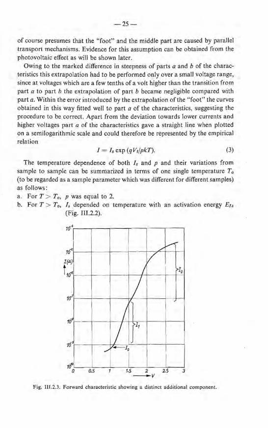
Fig. III.2.1 shows a typical set of In 1-Vi curves of one sample for different temperatures. As already mentioned in Chapter II, three different parts can be distinguished in these curves
(a) A very steep middle part with a slope of the order of q/2kT. (b) A region at lower voltages showing a considerable deviation toward
higher currents. This is the leakage discussed in Chapter II, to be denoted henceforth as the "foot" of the characteristic.
(c) A region at higher voltages where a considerable deviation towards lower currents occurs due to series resistance.
-1n15
t
20 L_ ___ ...J...._ _ __,'----'------'-----'
0 2 3 4-- 1000
T
Fig. III.2.2. Is VS r-1 for the junction of Fig. III.2. 1.
It should be borne in mjnd that the criterion by which the samples were selected for quantitative measurement was the occurrence of a pronounced steep mjddle part in the characteristics. Therefore the genera! appearance of the curves is to some extent a matter of selection and thus in itself does not imply very much. It should however be emphasized that parts b and c could be recognized in every sample. In the discarded samples, however, these parts occurred in adjacent or even in overlapping current ranges, thus obscuring the middle part, which plays a crucial röle in the interpretation. We therefore want to emphasize that the samples excluded by our method of selection <lid not basically ditfer from the accepted ones, but were merely less suitable for observing the interpretable aspects of their behaviour.
The curves were analyzed by extrapolating the "foot" toward higher voltages and subtracting this extrapolation from the steep middle part. This procedure
-25-
of course presumes that the "foot" and the middle part are caused by parallel transport mechanisms. Evidence for this assumption can be obtained from the photovoltaic effect as will be shown later.
Owing to the marked difference in steepness of parts a and b of the characteristics this extrapolation had to be performed only over a small voltage range, since at voltages which are a few tenths of a volt higher than the transition from part a to part b the extrapolation of part b became negligible compared with part a. Within the error introduced by the extrapolation of the "foot" the curves obtained in this way fitted well to part a of the characteristics, suggesting the procedure to be correct. Apart from the deviation towards lower currents and higher voltages part a of the characteristics gave a straight line when plotted on a semilogarithmic scale and could therefore be represented by the empirica! relation
I =Is exp (qVt/pkT). (3)
The temperature dependence of both Is and p and their variations from sample to sample can be summarized in terms of one single temperature To (to be regarded as a sample parameter which was different for different samples) as follows: a. For T > T0 , p was equal to 2. b. For T > T 0 , Is depended on temperature with an activation energy Eis
(Fig. III.2.2).
:-5 10
I(A
t1 )
0-6
rf
0-1.
ös
ö'IO 1 0
./
0.5
/ v-
/ / >I2
/ --~
/..
/ ! ~
>I1
v-1,1
1
1.s 2 2.s 3 ---v
Fig. Ilf.2.3. Forward characteristic showing a distinct additional component.

-26-
c. For T < To, p was somewhat larger than 2. d. For T < To, Is <lid not show a marked activation energy. e. Although T0 was different for different samples it never exceeded 700 °K.
A lower limit for To cannot be given because at lower temperatures (T < 300 °K) the steep part of the characteristics did not stand out clearly enough for accurate determination of p and Is.
f. Samples prepared from the same crystal often displayed different values of To.
The value of Is at room remperature, if evaluated from its exponential dependence on l/T for T > T0 , always corresponded to a current density of the order of 10- 19 A cm-2.
For most preparation runs the value of Eis was 1·43 eV. In one preparation run Eis was l ·55 eV. This preparation run also contained
some crystals that showed a definite "shoulder" on the steep part of the In l vs Vi characteristic (Fig. III.2.3).
R, R
Ia ~ "foot"
Fig. IIl.2.4. Circuit suggested by the curve of Fig. Ill.2.3.
The simplest scheme giving rise to such a "shoulder" is shown in Fig. IIl.2.4, which represents two parallel junctions 1 and 2, carrying currents li and h with series resistances R1 and R2; the whole shunted by the "foot" mentioned earlier, and in series with this system a resistance R. When we allot to these junctions characteristics h = Is1 exp (qVi/2kT) and / 2 = f s2 exp (qVi/2kD respectively, a characteristic like Fig. III.2.3 results if we take f s2 < fs1, R2 < Ri and R « R1. For the voltage range where the infiuence of the "foot" is negligible Fig. III.2.4 can under these conditions be replaced by Fig. III.2.5 without appreciable error. The latter scheme is accessible to quantitative analysis: For R2 « Ri this analysis would be quite simple since h can then be obtained
J;.'
F ig. IIl.2.5. Simplified version of Fig. IIl.2.4 for Ri » R , Ri > R2, 181 > fs2.
-27-
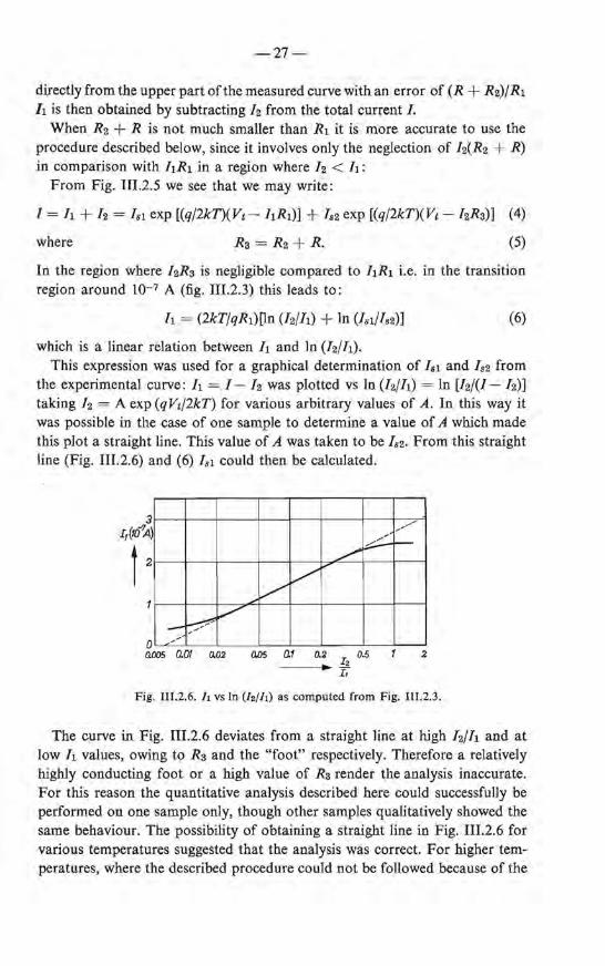
directly from the upper part of the measured curve with an error of (R + R2)/R1 /1 is then obtained by subtracting h from the total current /.
When R2 + R is not much smaller than R1 it is more accurate to use the procedure described below, since it involves only the neglection of h(R2 + R) in comparison with IiR1 in a region where h < Ii:
From Fig. 111.2.5 we see that we may write:
I = Ii + h = ls1 exp [(q/2kT)(Vt- IiR1)] + ls2 exp [(q/2kT)(Ve - hR3)] (4)
where R3 = R2 +R. (5)
In the region where /2R3 is negligible compared to IiR1 i.e. in the transition region around 10- 7 A (fig. 111.2.3) this leads to:
Ii = (2kT/qR1)Qn (/2/li) +In (lsi/ls2)] (6)
which is a linear relation between h and In (/2//i). This expression was used for a graphical determination of ls1 and ls2 from
the experimental curve: h = I - /2 was plotted vs In (h/li) =In [h/(J- /2)] taking h = A exp (qVe/2kT) for various arbitrary values of A. In this way it was possible in the case of one sample to determine a value of A which made this plot a straight line. This value of A was taken to be ls2. From this straight line (Fig. 111.2.6) and (6) lsi could then be calculated.
~ / -
0 / /
0.005 0.01 0.02
/ 1?
/ /"
0.05 at 0.2 I 2 0.5
----- I,
// /
-
2
Fig. III.2.6. /i vs In (hili) as computed from Fig. III.2.3.
The curve in Fig. 111.2.6 deviates from a straight line at high hili and at low h values, owing to R3 and the "foot" respectively. Therefore a relatively highly conducting foot or a high value of R3 render the analysis inaccurate. For this reason the quantitative analysis described here could successfully be performed on one sample only, though other samples qualitatively showed the same behaviour. The possibility of obtaining a straight line in Fig. 111.2.6 for various temperatures suggested that the analysis was correct. For higher temperatures, where the described procedure could not be followed because of the
-28-
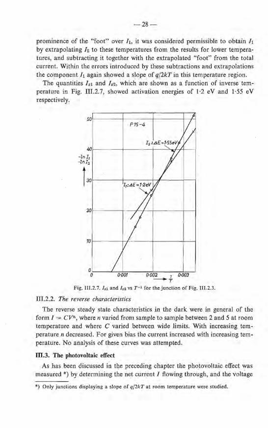
prominenèe of the "foot" over /i, it was considered permissible to obtain 1i by extrapolating /z to these temperatures from the results for lower temperatures, and subtracting it together with the extrapolated "foot" from the total current. Within the errors introduced by these subtractions and extrapolations the component Ii again showed a slope of q/2kT in this temperature region.
The quantities / 51 and fs2, which are shown as a function of inverse temperature in Fig. III.2.7, showed activation energies of l ·2 eV and l ·55 eV respectively.
P15-4
40>--~~~-+-~~~--+-~~..-+--++~~
-1nl1 -lnl2
î 30~~---+----I
01--~-'-~.........,~~~~~~~-'----' 0 0·002 7 0·003
-T . Fig. III.2. 7. l si and l s2 VS r -1 for the junction of Fig. III.2.3.
III.2.2. The reverse characteristics
The reverse steady state characteristics in the dark were in genera! of the form I = cvn, where n varied from sample to sample between 2 and 5 at room temperature and where C varied between wide limits. With increasing temperaturen decreased. For given bias the current increased with increasing temperature. No analysis of these curves was attempted.
ID.3. The photovoltaic effect
As has been discussed in the preceding chapter the photovoltaic effect was measured *) by determining the net current I flowing through, and the voltage
*) Only junctions displaying a slope of q/2kT at room temperature were studied.

-29-
drop Vt across the crystal as a function of light intensity and of shunting resistance Rs. Because the results on the <lark characteristics (see previous section) suggest that the "foot" consitutes a parallel transport mechanism, the net current through the junction proper was assumed to be the sum of the current Vi/Rs through the shunting resistance and the current which flows through the "foot" at the voltage Vi in the <lark. It should be noted that this assumption is valid only when the foot is relatively insensitive to illumination. Two typical forms of behaviour were found, shown in Figs. III.3.1 and III.3.2. For reference the <lark characteristics are also shown in the figures .
. Fig. III.3.1 illustrates the case where the net current steadily decreases as a function of Vt, even near the short-circuit situation (Vi = 0). In the figure a
I (A)
î v'>------+--- >-----+--____,,___________ ____ ____,
1Ö7r---- --+---- -t---- - -+-+-----<t------+------<
~----
:====:
W~t------1------+-.,.__--+--+----::::=: 10o/o-+-----i ,.,_, __ ..,,,..__ :=: ·-. ·-. ·----. 16~1-----7"<-t------+--+---+------t~to/c-----+-------1
I I
,"-qf2kT I I
m~'t------~-----+~'---~-----+----~---~ 0 0.5 1.0 1.5 2.0 2.5
--14(V)
Fig. Ill.3.1. Net current I vs total voltage Vt for various light intensities. For reference the dark characteristic has been included in the figure. Starting material: Recrystallized SiC.

-30-
diagram is included which shows that the relation between short circuit current, indicated in arbitrary units by A, and light intensity, indicated in arbirtary units by B, is approximately linear in the investigated range of two decades. The behaviour illustrated in Fig. IIl.3.1 was found in preparation runs which were made using recrystallized technical grade SiC as starting material (see Chapter Il).
In Fig. IIl.3.2 the other typical kind of behaviour is shown. It is seen that the steady decrease of the net current at low voltages is not observed. The relation of light-intensity and short-circuit current is still more linear here. It should be pointed out that in this case the short-circuit current was always an order of magnitude lower than in the previous one under the same light intensity. (The curves for highest illumination level in both figures correspond to the same light intensity.) The behaviour illustrated in Fig. 111.3.2 was found when technica! grade SiC was used as starting material.
I I I
I~) I
f 10~8----+-----+-----+-1--~-E! 100°
I I I I I
1------+-_.,,.'"---+----+-->--- :===: 10% I :==: / :::=:
Dark characterlstic / I
·-· ·-r--r----;-----+---,__---+----+-To/o
f'%kT I I I I
10-11 o-~---o~.s~---tLo_,__ __ 1~.s----2.Lo _ __ __.
-l't(V)
Fig. 111.3.2. Net current I vs total voltage Vi for various light intensities. For reference the dark characteristic has been included in the figure. Starting material : Technica! grade SiC.
Another difference should be mentioned between the junctions having the properties which are illustrated in Fig. IIl.3.1 and those that display the behaviour shown in Fig. 111.3.2. In the former case the transient response to a change in either voltage or illumination level was very slow. After any such a change a steady state was reached only after several minutes. The Jatter category of junctions reacted much faster: Steady state measurements on them could immediately be performed after any isothermal change of circumstances.

-31-
ill.4. The spectral distribution of the p-n luminescence
III.4.1. Forward bias
F or photon energies which are larger than the band gap it was thought relevant to compare the spectra! distribution of the emitted light with the theory of van Roosbroeck and Shockley 1) for band-band transitions in semiconductors. Using the idea of detailed balance these authors were able to correlate the spectra! distribution / 0(v) of band-band transitions as generated in the crystal to the (energy dependent) absorption coef.ficient by means of the relation
/ 0(v) = [87Tn2/c2h2]{h2v2a(v)/exp (hv/kT)}
where n is the refractive index., h Plancks' contant, c the velocity of light and where the factor in square brackets can be considered as a constant in our case 2).
This theory therefore is quite general, all infl.uences of band structure, transition probabilities etc. being accounted for by the absorption coefficient which can be determined experimentally. Moreover in this region the absorption coefficient does not depend on the impurity content of the semiconductor and therefore values given in the literature for the absorption coef.ficient can be used.
25
i 10
5
0
8·76 39·2 121 216 - a (cm-1J 4·33 18·9 m 1• s 363
1 1
- >-- experiment -- --- theory
\
\ \
' \ ---,,\
' \
\ \
1\ 2·7 2fJ 2·9 3 3·1 3·2 3·3
-E(eV)
Fig. III.4.1. Spectra! distribution of the p-n luminescence under forward bias, corrected for self-absorption by using d as adjustable parameter.
-32-
On other hand it should be noted that because of this connection between emission and absorption one should not expect to obtain from the emission spectra fundamental information which is not already contained in the absorption spectra.
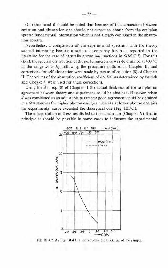
Nevertheless a comparison of the experimental spectrum with the theory seemed interesting because a serious discrepancy has been reported in the literature for the case of naturally grown p-n junctions in 6H-SiC 3). For this check the spectra! distribution of the p-n luminescence was determined at 400 °C in the range hv > E0 , following the procedure outlined in Chapter II, and corrections for self-absorption were made by means of equation (8) of Chapter II. The values of the absorption coefficient of 6H-SiC as determined by Patrick and Choyke 4) were used for these corrections.
Using ford in eq. (8) of Chapter II the actual thickness of the samples no agreement between theory and experiment could be obtained. However, when d was considered as an adjustable parameter good agreement could be obtained in a few samples for higher photon energies, whereas at lower photon energies the experimental curve exceeded the theoretica! one (Fig. 111.4.1).
The interpretation of these results led to the conclusion (Chapter V) that in principle it should be possible in some cases to influence the experimental
25
5
0
8·76 39·2 121 276 - a(cm-1)
4· 3 18·9 73-4 195 363
1 1
- - experiment -- ---- theory
\
' \ ''\
\ \
~ 1 i
2·7 2·8 2·9 3 3·1 3·2 3'3 --.E(eV)
Fig. IIl.4.2. As Fig. IIl.4.1. after reducing the thickness of the sample.

-33-
spectrum by removing part of the junction. Therefore the thickness of the sample, the behaviour ofwhich is illustrated in Fig. IIl.4.1, was reduced from its initia! value of 360 µ to 140 µ. This resulted in a strong decrease of the discrepancy between theory and experiment. The parameter d in eq. (8) of Chapter II had to be adjusted in both cases to the same value of 50 µ. Moreover the wavelength at which the discrepancy became notable was the same in both cases (Fig. IIl.4.2).
111.4.2. l?everse bias
As noted in Chapter II, the small light-emitting "blue spots~ ' were observed in all samples when high reverse currents were passed througb them. In genera! these "blue spots" were situated at or very near the surface of the sample, in the p-n junction. They could individually be influenced by picking with a needle, by sandblasting and by putting the sample in a fluid dielectric. An increase of the current resulted in an increase of the number of the spots, but also, in m_any cases, in an increase of their brightness, though their spectra! distribution remained essentially the same. No attempt has been made in this work to study _these "blue spots" in -any detail.
REFERENCES
1) W. van Roosbroeck and W. Shockley, Phys. Rev. 94, 1558-1560, 1_954. 2) H. R. Philipp and E. A. Taft, Proc. SiC Conf. 366-370, 1960. 3) L. Patrick and W. J. C hoyke, Proc. SiC Conf. 28Jc305, 1960. 4) W. J. Choyke and L. Patrick, Proc. SiC Conf. 307-311, 1960.

CHAPTER IV
THEORETICAL CONSIDERATIONS
IV.l. Introduction
The experimental results on the steady-state forward characteristics of the junctions studied in this work would seem to be in good agreement with the theory of Herlet and Spenke 1) for p-i-n junctions: For high forward bias this theory predicts, as has been mentioned in Chapter I, a characteristic of the form
I = Is exp [- sinh (d/Lt) gd (d/Lt)] exp (qVt/2kT) (1) where
Is = 2qnt (Lt/Tt) tanh (d/Lt) (2)
For high injection levels the lifetime and diffusion length of injected carriers in the i-region are expected to be not very dependent on temperature 2), which would meao that the saturation current Is should depend on temperature solely by nt, i.e. with an activation energy of half the bandgap. lndeed an activation energy of 1 ·43 eV was found in most samples, the bandgap of 6H-SiC being 2·86 eV. Reasonable values of lifetime Tt , diffusion length Lt and width of the i-region d are required to have at room temperature
Is exp [ - sinh (d/Lt) gd (d/Lt)] ~ 10-19 A cm-2
as was found experimentally. Furthermore the slope of the In I vs Vt curves was found to be in many
cases q/2kT, as required by (1). This agreement between the experimental results and the theory
of Herlet and Spenke is rather remarkable, because in the derivation of this theory it has been assumed 1) that electrons and holes have equal mobilities, and that no trapping occurs (see Chapter I). In addition, equations (1) and (2) are approximations for the case that the lifetime ofinjected carriers is independent of injection level, which need not always be so when trapping occurs.
In view of the agreement between our experimental results and the theory of Herlet and Spenke it seems that a further development of the theory for the case where electrons and holes have different mobilities and where trapping does occur is worth while, especially when the influence of illumination is included. This will be attempted in the present Chapter.
The assumptions made in the following sections are considered to be rather realistic for the case of SiC. Their validity will be discussed in detail in Chapter VI, where the results of the present Chapter and those of Sections 2 and 3 of Chapter III will be confronted with each other.
In section IV.2 the assumptions which have been made are discussed. Section IV.3 describes the solution of the continuity equations in the i-region, while

-35-
in Section IV.4 the solution of these equations in the p- and n-regions is considered. In Section IV.5 the boundary conditions are evaluated, after which (Section IV.6) the total current can be derived as a function of the sum of the voltage drops over the harriers. The result thus obtained proves to be very complicated. Therefore we consider in the following two Sections two simple cases: Section IV.7 is concerned with the unilluminated p-i-n junction and in Section IV.8 the illuminated p-i-n junction is treated in considerable detail under the simplifying assumption that the trapping and the mobilities are such that the Dember-field can be neglected everywhere in the i-region. It will be shown afterwards (Section IV.9) that junctions in which this assumption is not valid should in many cases display essentially the behaviour that is predicted by the simplified theory of Section IV.8.
IV.2. Assumptions
Apart from some restrictions that will be introduced later on, the following assumptions will be made throughout this Chapter:
(l) The structure under consideration will be taken to have planar geometry and will accordingly be described in terms of one coordinate x.
(2) In order to neglect the influence of the contacts on the behaviour of charge carriers, the contacts will be taken to be situated sufficiently far away from the p-i and i-n junctions and to be unilluminated, i.e. in the mathematica! treatment the generation of charge carriers by light will be assumed to be uniform, and the contacts are simply ignored. Later on (Chapter VI) we shall evaluate the corrections which are necessary in order to apply the theory to our experimental results, which were obtained under non uniform illumination (see Section II.2.3).
(3) Injected carriers in the p-, i- and n-regions will be supposed to have lifetimes which are independent of injection level.
(4) The continuity equations will be solved using the "space charge neutrality approximation", which is most conveniently described in terms of Poisson's equation:
dE - = (47Tq/e) [Llp + Llper - Lln - Llntr]. dx
The basic assumption of the space charge neutrality approximation is:
(e/47Tq) 1 ::1 « Llp + Llptr, Lln + Llntr
which permits us to write instead of (3):
Llp + Llptr = Lln + Llntr.
(3)
(4)
(5)
lt should be emphasized however that this does not imply that dE/dx is taken to be equal to zero, i.e. that the space charge is neglected. The validity of this

-36-
approximation under various circumstances will be discussed elsewhere 3). lts significance may be described in the following way. In general injected electrons and holes have different probabilities of being trapped and different diffusionconstants. Therefore one of the two kinds of charge carriers will in general tend to diffuse faster than the other, and consequently an electric field is generated, which tends to reduce the difference between the two partial currents. In the "space charge neutrality approximation" this field, known as the Dember-field,
· is taken in to account, but the difference between the concentrations of electrons and holes which gives rise to it is neglected (eq. 5).
It should be emphasized that the considerable space charge in the p-i and i-n junctions is of course not neglected in this treatment: We shall not use (5) in connection with these barriers.
(5) The generation and recombination in the harriers will be assumed to be negligible in comparison with the generation and recombinatlon elsewhere. This assumption allows the concentrations of charge carriers of the same kind on both sides of and immediately adjacent to these regions to be connected with Boltzmann statistics 4) (See also Section I.5). In this case the continuity equations need only to be solved in the p-, i-, and n-regions separately, since the assumption provides the boundary conditions by which the obtained solutions can be connected with each other.
(6) The trapping probability of injected holes and electrons will be taken to be independent of the injection level in the intrinsic region. This assumption is justified in the case of sufficiently shallow trapping centers which can only trap either electrons or holes. When this assumption is satisfied, it is permissible to write for the steady state:
Llntr = KnL1n L1ptr = KpL1p
wherè Kn and Kp are constail.ts. Su bstitu tion of these relations in ( 5) yields:
(L1n/L1p) = (1 + Kn)/(1 + Kp) =K. (6a)
In the steady state the recombination rates of electrons (Lln/-rni) and holes (Llp/-rpi) are equal *). Therefore we have from (6a):
(-rni/Tpi) = K, (6b)
(7) The injection level in the i-region will be taken sufficiently high to justify the approximation
L1n = n Lip ~ p.
Consequently we have (eq. 6a) (n/p) = K, (7)
*) Writing the steady state recombination rate of e.g. electrons as (.tJn/Tnj) is in fact the same as defining the steady state e!ectron lifetime Tnt· We shall later obtain expressions for rn1
and r pt by means of this definition.

-37-
JV.3. The solution of the continuity equations in the i-region
In the i-region where (7) applies, the current equations:
dn
can be written as
ln = qnµnE + qDn -dx
dp lp= qpµpE- qDp--c
dx
dn ln = qnµnE + qDn -
dx
(8)
(9)
(10)
(11)
We now introduce the Dember-field L1E, which is defined by the relation
E = [J/qn(µn + K - 1µp)] + L1E (12)
where J is the total current In + lp. Substituting (12) in (10) and (ll) yields after some simple algebra:
(13)
(14)
µ - K-lµ 1 dn L1E = -(kT/q) n . P - -
µn + K-1µp n dx (15)
with (16)
The introduction of the ambipolar diffusion constant D has the following advantage. According to (13) and (14) the ambipolar diffusion terms cancel each other in the total current J = In + lp, in contrast to the ordinary diffusion terms in (10) arid (11). This has been accomplished by separating the Dember field L1Efrom the total electric field E, thus obtaining in (13) and (14) quasidrift terms w,hich are independent of x. Therefore the continuity equations
acquire the simple form
q-1 div In = (n/rni) _..:._ g
q-1 div lp = - (p/rpi)+ g
d2n · D - = (n/rni) - g
dx2
(17)
(18)
(19)

-38-
(20)
where g is the generation of carriers by light, which we took to be uniform. The genera} solutions of (19) and (20) are:
n = C1 exp (x/Lt) + C2 exp (-x/Li) + g-rnt
p = K-1C1 exp (x/Lt) + K-1C2 exp (-x/Li) + g-rpi
where C1 and C2 are integration constants and where
(21)
(22)
(23)
A similar type of diffusion length has been used previously 5) for the case that J = 0. The procedure followed above is simply an adaption to the present case of the idea of ambipolar diffusion, which has been introduced in semiconductor physics by van Roosbroeck 6). The diffusion length Lt depends on the trapping parameter K and is independent of injection level, as can be seen by substitution of (16) into (23). It can be shown 3) that in genera! for very low and very high injection levels the diffusion length does not depend on trapping and that in the intermediate range of injection levels the diffusion length does depend on the injection level. In the present case the situation may be described by saying that we have high injection levels as far as recombination is concerned (Lln = n, Lip = p) but low injection levels as far as trapping is concerned (n = Kp).
Eqs (21) and (22) immediately yield the contribution of the intrinsic region to the total net recombination and thus to the total current (see equation (3) of Chapter l). When we take the i-region to be situated between x = -d and x = +d we have:
+d J<t> = q f [Lln/-rnt) - g]dx = 2q(C1 +C2)(Lt/-rnt) sinh (d/Lt). (24)
- d
IV.4. The solutîon of the continuity equations in the p- and n-regions
lt is well known 7) that in the n- and p-regions the continuity equations for minority carriers have the same form as. (19). The main difference is that one can use here the diffusion constant of the minority carriers themselves (the appropriate ambipolar diffusion constant being equal to it). Although in this case the quasi-drift terms, analogous to those in (13) and (14), are not independent of x, we need not bother about them because they are negligible 7).
One may thus write for e.g. holes in the n-region :
d2p Dp - = (Llp/-rp) - g.
dx2 (25)

-39-
Under the boundary condition Lim L1p = gTp, which is a consequence of as-x-+oo
sumption 2 the solution of (25) may be written:
L1p = Ca exp [-(x-d)/Lp] + gTp.
In the same way as in the case of the i-region this leads to
J<n> = Jp( +d) = (qLp/Tp)Ca.
Similarly we obtain for electrons in the p-region:
L1n = C4 exp [(x+d)/Ln] + gTn
J<Pl = Jn(-d) = (qLn/Tn)C4.
IV.5. Evaluation of the boundary conditions
(26)
(27)
(28)
(29)
As bas been noted already the constants C1 through C4 must be determined by connecting the carrier concentrations on both sides of the two harriers by Boltzmann statistics. In order to do this the distribution of voltage drops over the p-i-n structure needs to be considered first. Any voltage drop Vt over the structure in principle consists of 5 components: two resistive voltage drops over the p- and n-regions, the voltage drops Vi and Vr over the p-i and i-n harriers, and an additional voltage drop Vi over the i-region. The first two of these may be neglected in our case, because they do not enter the theory in an essential way, which leads to:
Vi = Vi + Vi + Vr . (30)
Herlet and Spenke 1), whose treatment is closely followed here, have already shown that Vi need not enter into the theory itself. Vi has to be evaluated in terms of Vi and Vr however, when one wants to connect the current flowing through the junction with the experimentally relevant voltage Vt. We have according to Boltzmann statistics in the i-region 1):
p(-d) = nt exp (qVz/kT), n( +d) = nt exp (qVr/kT). (31a)
When substituted into (7) these equations yield:
n(-d) = Knt exp (qVi/kT), p( + d) = K-1nt exp (qVr/kT). (31b)
In the n-region p( +d) is given by multiplying p( +d) in the i-region by the appropriate Boltzmann factor:
p( + d) = K-lpn exp (2q Vr/kT). (32a)
Similarly for the p-region we have:
n( -d) = Knp exp (2q Vi/kT). (32b)

-40-
IV.6. The evaluation of the current J in terms of Vz + Vr; the voltage drop V t over the i-region
The total current can now be derived as a function of Vz + Vr only. In view of the Iength of the derivation only an outline is given here, together with the results. The full argument is presented in Appendix A. From (31) and (21) one can easily calculate (C1 + C2) and (C1 - C2) in terms of Vz and Vr. Substitution of ( C1 + C2) in (24) then yields J<t> as a function of Vi and Vr. In the same way J<n> is obtained as a function of Vr from (26), (27) and (32a), while J<P> is derived analogously. The total current is then,found as a function of Vz and Vr by noting that J....:. J<t> + J<n) + J<P> (eq. (3) of Chapter 1).
The additional relation between Vz and Vr, which is needed to obtain J in terms of V = Vz + Vr, i.e. the total voltage drop over the two harriers, can be obtained from the hitherto unused condition thatin the steady state the currents through the two harriers must be equal:
ln(-:d) + Jp(-d) = l n( +d) +lp( +d). (33)
All terms in (33) can be evaluated by means of the relations obfained hitherto. In particular Jp('--d) and 171( +d) can be obtained by substitutîon of dn/dx
from (21) in (13) and (14), using the values already found for C1 and C2. Furthermore ]71(-d) = j(P) arid Jp(+d) = J<n>.
When the injection of minority carriers from ·the i-region in to the p- and n-regions is neglected (see Appendix A), the result of these calculations can be conveniently written down using a parameter Il, to be referred to as the asymmetry parameter and defined as
Il= (q/2kT)(Vi-Vr) +-!In K, (34)
Under the condition that in the n- and p-regions the minority carrier concentration is much larger than the equilibrium value and that in the i-region n and p are much larger than ni, i.e. under the condition that Vz and Vr are positive and large enough to give high injection, the thermal generation can everywhere be neglected. We thus find (see Appendix A):
J = 2q(Lï/VTnfrpt) tanh (d/Lt)nï exp (qV/2kT) cosh Il-- 2qgLt tarih (d/Lt) - qg(Ln + L p) (35)
where • l~ fl-n - K- lfl-p
smh Il = (VTniTpif2Ltnt)tanh(d/Li) exp(- qV/2kT)[g(Ln- Lp)+ . 1 J]. q(f.Ln + K- f.Lp)
(36) For convenience we also quote here the expression which is obtained in
Appendix A for the electron concentration in the intrinsic region: Under the condition that n and p are much larger than nt in the i-region, the electron concentration in this region is found to be:
~41-
[ cosh (x/Li)] V- · cosh (x/Li) n = gTni 1 - + ni K exp (qV/2kT) cosh S b (d/ ) -
cosb (d/L t) cos Lt
V- sinb (x /L i) nt K exp (q V/2kT) sinh S sinh (d/Lt). (37)
Equations (35) and (36), which are coupled by the asymmetry parameter S, in principle constitute the solution of the problem under discussion. Together they give, though implicitly, the relation between the current J and the total voltage over the harriers V as a function of illumination level g and of the different parameters which determine the properties of the junction . . ... The various terms in these relations and in (37) can be interpreted as follows :
The first term in (35) represents the recombinationjn the i-region of electrons and holes, that have been injected from the n- and p-regions respectively. The second term represents the current of electrons and holes that have been generated by the illurnination within a diffusion length from the two harriers, in the i-region. When the i-region becomes small (i.e. d « Lt), the two .effective layers of thickness L t overlap, hence the occurrence of the factor tanh (d/Lt) in this term. The third term bas an analogous meaning. It accounts for the generation of carriers near the two harriers in the p- and n-regions.
The parameter S occurs because of the asymmetry between holes and electrons. It can be seen from (36) that in the case of complete symmetry between the two kinds of carriers, i.e.
K = 1 µn = µp
Ln=Lp
we have S = 0 and consequently cosb S = 1. Hènce for g = 0, K = 1 and µ n = µ p, (35) reduces to the expression obtained by Herlet and Spenke. The first term in the second member of(37) describesthe modulation of the resistivity of the i-region by the illumination. Therefore it will henceforth be referred to as the photoconductivity term~ At x = ± d this term vanishes, because carriers generated near the harriers are drawn into the adjacent regions, giving rise to the seond term in (35). The other terms describe the injection of charge carriers into the intrinsic región. The second is symmetrical in x and the third asymmetrical. Again when S = 0 this last term vanishes.
In order to evaluate Jas a function of the total voltage drop Vi, which is, in contrast to V an experimentally accessible quantity, it is necessary to calculate the voltage drop oyer the . i-region Vi, which does not occur iil the equations obtained hitherto.
Obviously we have : +d
. Vi = f Edx . (38) - d

-42-
According to (12) and (15) one may write:
J E=-----
qn(µn + K-1 µp)
kT JLn - K-1µp 1 dn
q JLn + K-1 µp n dx (39)
In principle (39) can be integrated over the i-region since n and dn/dx are known as a function of V from (36) and (37). Though it is possible to eliminate S from (35) and (36), the resulting explicit relation between J and V is very cumbersome, while in general the actual integration of (39) gives complicated results also. We shall therefore proceed by treating first two simplified cases (sections IV.7 and IV.8). One of these will be shown in Chapter VI to be in very good agreement with our experimental results. The study of these simplified cases will provide a physical understanding of the expressions obtained hitherto. Moreover it will provide a convenient starting point for the qualitative consideration of still another important case in section IV.9.
IV.7. The dark case
In the dark (i.e. g = 0) substitution of (35) into (36) yields
sinh S = u cosh S
where u is a constant given by
u = [(µn - K-lµp) /(µn + K-lµp)] tanh2 (d/L.,,).
Substitution into (35) then yields
(40)
(41)
J = 2qn.,,(Lt/VTnfTpi)(1 - u2)-t tanh (d/L.,,) exp (qV/2kT). (42)
From (40) and (37) we obtain:
[cosh (x/Li) sinh (x/L.,,)] n = [K/(l - u2)]t nt exp (qV/2kT) - u - .- --
cosh (d/Li) smh (d/L.,,)
From (43) and (42) it is seen that we may write
n = f(V)g(x) and J ocf(V).
Consequently the ohmic component of Vt, given according to (39) by
+d Vt!J = [J/q(µn + K-1µ.p)] f n- 1 dx
-d
is independent of V. The Dember component of Vt can be written according to (39)
lnn(+d)
kT JLn - K- 1µp J Vin =-- - - - -q JLn + K-lµp
lnn(-d)
d ln n.
(43)
(44)
(45)

-43~
Using (31), (34), (40) and (41) we obtain from (45):
2kT µ 11 - K-lµp . [ µ 11 - K-lµp · J .,. Vin= - - artanh tanh2 d/Lt) . {46)
q J.Ln + K-1µp µn + K~1µp .·
From ( 46) it is clear that Vw is always positive under the conditions which led to this result, i.e. in darkness and under forward bias. It should furthermore be noted that Vin is constant also. Therefore the dark characteristic should display a slope of q/2kT for high forward bias.
IV.8. Explicit evaluation of the photovoltaic effect under the assumption th11t in the i-region J.Lnn and fl-PP are equal
IV.8,1. Introduction
We shall now consider the matherilatically most siniple case which still shows the typical differences between a p-i-n junction and a p-n junction when they are illuminated, i.e. we shall assume that in the i-region we have:
(47)
As can be seen from (13) and (14) this is equivalent with the assumption that in the i-region the quasi-drift terms in the electron and hole currents are equal everywhere. From (15) it can be seen that. in this case the Dember-fi~)d LJ,e is zero in the i-region also. Therefore (eq. (39)) Vi is equal to zero when J = 0, A further simplification accomplished by assuming (47) beç:omes apparenton inspection of (36): The term containing J in this relatiQn vanishes when ( 47)
is substituted. '· ; It will be shown later (Section IV.9) that junctions in which (47) is not
valid should in many cases display essentially the behaviour . th~t .~s
predicted by the simplified theory of the present Section. , ,
IV.8.2. Terminology
In the following discussion various quantities will be used which are familiar already from the literature on the photovoltaic effect of ordinary p-n junctions. lt is, however, necessary to give new definitions of these quantities, due to the fact that a p-i-n junction has. two barriers over which voltage drops Vz anci Vr can be ~aintained and between these an intrinsic region over which a voltage drop Vi can occur.
(1) The photocurrent
In the literature this term is sometimes used to indicate the current of lightgenerated carriers, i.e. as the quantity lpa in eq. (11) of Chapter 1. We shall generalize the idea of photocurrent by defüiing it as the change in the current which comes about when the junction is illumioated while the total voltage drop over the harriers is kept at its dark value. It should be noted that under

-44-
illumination the total bias Vi has to be changed wben V must keep its dark value, in order to compensate for the change in Vt. We shall therefore refer to the photocurrent defined in the above way as to the "Equivalent Bias Photocurrent", denoted by hBP· The advantage of the present definition of photocurrent is the elimination of.the unessential voltage drop Vt from the argument. For ap-njunction lEBP and /pk are identical since in such ajunction we have V= Vt.
(2) The short circuit current
The current which fl.ows through the junction when the total voltage drop .Vi is equal to zero will be referred to as the short circuit current. In contrast to the case of an ordinary p-n junction the short circuit current of a p+n junction is not equal to the photocurrent, as will be shown in due course.
It should be emphasized that in the short circuit situation we have V = -Vi, and not as one might perhaps think V = Vt = 0, in contrast to the case of a short circuited p-n junction with negligible series resistance. In fact, as will be shown 1 VI = 1 Vil can have large values even under moderate illumination when Vi = 0.
(3) The open circuit voltage
We shall use two kinds of open circuit voltage, V0cth and V0cexp • V0cth will be the total voltage over a p-i-n structure when the current J through the junction
is equal to zero. In this case we have Vi = V, as will be clear. V0 cexp will be the total voltage drop over a sample when the current through it is equal to zero. Vocexp can differ from V 0cth owing to leakage phenomena (e.g. the "foot" of our experimental characteristics) and also because of nonuniform iHumination (see Chapter VI). Note that in contrast to a well-known property of p-n junctions in the case of a p-i-n junction the relation between JEPB and V0cth is not the same as the relation between J and Vt in darkness. The reason for this is tbat in the open circuit situation Vi = 0, while in darkness for J :f=. 0 we always have Vi :f=. 0.
IV.8.3. The Equivalent Bias Photocurrent as a function of total harrier voltage
The photovoltaic effect of a p-i-n structure in which (47) is satisfied can be conveniently described in terms of lEBP when we rewrite (35) and (36) in the following way:
J = J8 exp (qV/2kT)- 2qglt tanh (d/L,)- qg(Ln+Lp) + + }8 (cosh 8 - l)exp (qV/2kT) (48)
where
Js = 2q(Lt/V-rntTpt) nt tanh (d/Lt) (49) and
sinh 8 = g(Ln-Lp)(V-rntTpt/2Ltnt) tanh (d/Lt) exp (-qV/2kT). (50)

-45-
The asymmetry parameter S is given, as has been shown already, by
S = (q/2kT)(Vi-Vr) +-!-In K. (51)
From (50) we see that for g = O we have S = 0. Eq. (48) then gives for the da~k current Ja
Ja= Js exp (qV/2kT). (52)
Therefore we may write by definition (see eq (48)):
Jesp = 2qgLi tanh (d/Lï) + qg(Ln+Lp) - Ja (cosh S- !). (53)
Furthermore (50) can be reduced to
sinh S = [qg(Ln-Lp)/Ja] tanh2 (d/Lï). (54)
According to (53) and (54) we have for tanh d/Lï ~ 1:
Ja «qg!Ln-Lpi: Jesp =2qgLt tanh (d/Lt) +qg(Ln+Lp)-qg!Ln-Lpl = = 2qgLï tanh (d/Lï) + 2qg Min (Ln, Lp) (55a)
(55b)
It can easily be shown that
(56)
Thus with increasing Ja, and hence with increasing V, JesP increases from the value given by (55a) to the value given by (55b). These two values are equal when Ln =Lp, in which case Jesp does not depend on V;
It can be seen what physically happens by retracing qualitatively the above calculations, assuming for the sake of argument that Ln > Lp. .
Noting that light-generated carriers, which are collected by a harrier, always give rise to a negative current through that harrier (eq. (11) of Chapter I), we see that when the junction is illuminated while Vis kept at its dark value, the p-i harrier (which is the more efficient collector for Ln > Lp) increases its bias Vi in order to conserve the continuity of current, and therefore the i-n harrier decreases its bias Vr. At high V these changes in Vi and Vr are much more effective due to the exponential dependence on Vof carrier concentrations etc. Therefore, for a fixed value of g(Ln-Lp), the asymmetry introduced and accordingly the change in total recombination in the i-region is smaller when V is high than when Vis small. In fact we see from (55b) that upon illumination for high values of V the change of the total recombination in the i-region is nil, and that therefore all light-generated carriers contribute to Jesp. Eq. (55a) shows that for low values of V the surplus generation near one harrier, i.e. glLn- Lpl is compensated by an equal amount of extra recombination in the i-region: For Ln > L p, Vi increases sufficiently to inject for every surplus

- 46-
electron an extra hole into the i-region where they recombine. Consequently the surplus electrons cannot contribute to lEBP·
IV.8.4. The evaluation of Vi as a function of l for la » qglL n-Lpl
For the evaluation of Vi as a function of l we sball restrict ourselves to the range of voltages V where lEBP is constant and given by
lEBP = 2qgLi tanh (d/Li) + qg(Ln+Lp). (57)
It has been shown in the previous subsection that this is the range where
Ja » qg/Ln-Lpl
and consequently (see eq. (54)):
sinh S « 1.
(58)
(59)
Furthermore we shall confine our attention to the range of total voltages
(60)
which is experimentally more readily accessible than the range Vt ;;::, Vocth.
Combining (48) and (53):
l = ls exp (qV/2kT)- lEBP =la - leBP (61)
we see that, since we have in the open circuit situation V = Vt = Vocth, the range of voltages specified by (60) is also given by
ls exp (qVt/2kT):::::;: leBP· (62)
It is shown in Appendix B that V and Vt depend monotonically on each other wben (60) is fulfilled. Therefore we may write instead of (62):
Ja = Js exp (qV/2kT) :::::;: lEBP (63)
since in the open circuit situation V = Vt. Witb the aid of the relations derived in this subsection we are able to
distinguisb the extreme possibilities as to the modulation of the resistivity of the i-region, which is obtained for this case by substitution of (59) in (37) :
[ cosh (x/Li)] f,; cosh (x/Li) n = gTni 1 - cosh (d/Li) + nt K exp (qV/2kT) cosh (d/Li,). (64)
(a) Li « Ln, Lp with d/Lt > 1. In this case the resistance of the i-region is governed by photoconductivity as we shall show.
When Lt » Ln, L p we have
leBP = 2qgLt tanh (d/Li). (65)

-47-
Thus Ja can simultaneously satisfy (63) and (58) which is demanded by the consistency of our treatment. Eq. ( 65) gives with ( 63) and ( 49) :
(66)
Therefore the photoconductivity term in (64) prevails over the injection term except at x;:::; ± d. Using (65) and (49) we can rewrite (64) in the convenient form:
(67)
Substitution of (67) into our expression for the electric fieldstrength in the i
region (39), using also (47) now yields by conventional calculus:
+d J 1 + A Vi = f Edx = (2kT/q) - sinh (d/Li) In -- (68)
-d VJ EBP2 cosh2 (d/Li) - 1 2 1 - A
where
l/lEBP cosh (d/Lt) - J A = tanh (d/2Lt).
lEBP cosh (d/Li) + J . (69)
b. The other extreme, i.e. the case where injection prevails in the i-region, can be realized for a range of voltages with Vt :( V0cth if the conditions
(70) are satisfied.
Here we obtain from (53) and (70):
iEBP = qg (Ln + Lp). (71)
According to (58), (63), (70) and (71) it makes sense to consider the range
Max [2q g Li tanh (d/Li), q g ILn- Lpl] « la :( q g (Ln + L p)
where by obviously have:
gTni « ~nt exp (qV/2kT). (72)
From (72) and (64) it is seen that unless d » Li injection now prevails in the entire i-region, and that consequently we may approximate n by
n = nt v; [cash (x/Li)/cosh (d/Lt)] exp (qV/2kT). (73)
Substitution of (73) and ( 47) in (39) now gives:
+d J Vi = f Edx = (2kT/q) sinh (d/Li) gd (d/Lt) (74)
-d J+iEBP
d!L1
where gd (d/Li) = f (cosh y)- 1 dy = 2 arctan [exp (d/Li)] - rr/2. (75) 0

-48-
1t should be noted that for JEEP= 0 (74) reduces to the expression already given by Herlet and Spenke wbich was quoted in Chapter 1 (eq. 9).
IV.8.5. The evaluation of Jas a funcion of Vi for constant JEEP
In the previous section we calculated Vi as a function of J for two extreme cases, i.e. the photoconductivity case and the injection case. In both cases the result showed that Vi is a funcion of d/Lï and of J/leEP only. Fora fixed value of d/Lt we can therefore write:
Vi = f(J/JEEP). (76)
Rewriting (61) as V = (2kT/q) In [(J + lEEP)/ls] (77)
we thus obtain for both cases:
Vi(J,leEP, ls) = (2kT/q) In [(J + JEEP)/Js] + f(J/lEEP). (78)
From (78) we derive
Vi(aJ, alEEP, ls) = Vi(J, lEEP, ls) + (2kT/q) Ina (79) and
Vi(J, leEP, hls)= Vi(J, JEEP, ls)- (2kT/q) In b
where a and b are arbitrary constants.
,_ "' ~ "'
10~~---~---~---~---~---~
"' 1021-----+-----+-----+-----t---t-'~--; '( >-)'
1'-----~----'------'----'--'-----' 0 0.5 1.0 1.5
-lif -v
2.0 2.5
(80)
Fig. IV.8.1. In (- J) vs Vt for the photoconductivity case. For reference the curve J = Js exp (qV/2kT) for the value of Js that was used in the computation of the curves has been included in the figure.

-49-
.... ~ 1021---~~~-+-~~~--+-~~~--++-~~~+-~~~~ "'
'? ~
1.s -11 -v
Fig. IV.8.2. As Fig. IV.8.1. Injection case.
From (79) and (80) it is clear that all ln (-J) vs Vi curves are of identical form. Variation of 18 results in a translation in the directioo of the Vt-axis and variation of lEBP results in a translation in a direction with slope q/2kT, over a factor a.
Volls
100 100
0. O.O O.f 0 234 0 234 0 23 4
--d -.1.. _.si... T; L; L;
î
/ /
i/
/ /
1
0.
/ / v
1 / /
/ '
/ v v
/ /
/
10
t
Fig. IV.8.3. sinh (d/L;,) gd (d/Li); (2kT/q) sinh (d/L;,) gd (d/L;,) and i 01og [exp { sinh (d/L;,) gd (d/L;,) ] }] as a fnnction of d/L;,.

-50-
It is therefore in both cases sufficient to construct one set of theoretica] curves for some arbitrary value of l EBP and ls and for different values of d/Lt Such curves are shown in Fig. IV.8.1 for the photoconductivity case and in Fig. IV.8.2 for the injection case. It should be noted that in these figures for any value of l the value of Vis given by the curve for d/Lt = 0.
(In Fig. IV.8.3 the functions
sinh (d/Li) gd (d/Lt),(2kT/q) sinh (d/L~) gd (d/Li) and lOJog [exp {sinh (d/Lt) gd (d/Lt)}]
are given as a function of d/Lt. These curves have to be used in the numericaJ calculations of Chapter VI).
IV.9. Outline of the theory for the case that f-Lnn # f-LPP in the i-region (onder the simplifying assumption Ln = L p)
In the previous section we have treated the photovoltaic effect of a p- i-n
junction, assuming for the sake of mathematica! simplicity that in the i-region the relation
(81) was obeyed.
In order to get some insight into the severity of this restriction (for which no physical basis can be provided), we shall in this section briefty consider another simplified case, i.e. we shall drop (81) but, again for the sake of simplicity, we shall assume that
Ln = Lp. (82)
When we introduce the abbreviations
r f-ln - K-lf-lp ]2 B2 = 1 - · tanh4 (d/Lt)
lf-ln + K-lf-lp (83)
and l p = qg(Ln + Lp) + 2qgLt tanh (d/Lt) (84)
we obtain after substituting (82) into (36) and after elimination of o from (35) and (36)
(85)
where l p is the clark current of the junction given by (42). We also find from (35) and (36)
tanh o = ± Vi - B2 [J/(l + l p)]. (86)
When lis plotted vs lp from (85) an orthogonal hyperbola results. Since eqs (35) and (36) have been derived under the assumption that
V > 0, we only need to consider the part of this hyperbola which corresponds to la > 0. Furthermore we must require that an open circuit situation exists,

-51-
i.e. that we have for some positive value of Jd : J = 0. Under these conditions we can easily show from (85) that we may write:
J = 0: J d = J p/ B
Jd = 0: J = -(Jp/B2)(1 - V1 - B2)
dl - > 0. dla
It should be noted from (88) and (83) that we have for Jd = 0
(87)
(88)
(89)
(90)
Furthermore it can be seen from (85) that for !lal « J the current J is constant. We thus see that in this case the In (-J) vs V curves should have the same appearance as those obtained in section IV.8 (see figs IV.8. l and IV.8.2 for d/Li = 0). Since (85) is hómogeneous and Jd oc exp (qV/2kT) these curves transform into each other by translations in a direction with slope q/2kT
It wil! be clear also that for any value of B2 these curves can be easiiy plotted from (85), their shape being dependent on the value of B2 only. The voltage drop Vi over the i-region can be computed also. Similarly to the results of the previous section we shall show that for fixed values of d/Li and B2, Vi depends solely on J/Jp. Therefore the In (-J) vs Vt curves also transform into each other when translated in a direction q/2kT.
The Dember-component of Vi is obtained by substituting (31) and (34) in to ( 45):
Vin = (2kT/q) o f-Ln - K-Iµ p .
f-Ln + ~-lµp (91)
Comparison of (91) with (36) shows that Vin has the sign of J, i.e. between the open circuit and the short circuit situations Vw < 0. Apart from B 2,
Vw is a function of J/J p only, as can be seen from (86) and (91). The ohmic component of Vi is obtained from the relation:
+ d
ViQ = f [J/qn(µn + K- 1µ.p)]dx. (92) - d
In order to estimate ViQ for the "injection case" we first investigate the dependence of n on J and Jp. Neglecting the photoconductivity term in (37) we write:
V- [ cosh (x/Lt) sinh (x/Lt) ] n = ni K exp (qV/2kT) cosh o - sinh o . (93)
cosh (d/Lï) sinh (d/Lt)
Substitution of exp (q V/2kT) cosh o from (35) and (36) yields with (82):

-52-
y- [cosh (x/Li) sinh (x/Lt) ] n = nt K [(J + Jp)/Js] cosh (d/Lt) - tanh 0 sinh d/Lt)] · (94)
When (92) and (94) are combined we obtain, using (16), (23) and (49):
kT 4DnDp K-1 J Vin= q (Dn + K-lDp)2 tanh (d/Lt) J +lp
+d!L1
- - tanh ó d (x/Li). (95) f lcosh (x/Li) sinh (x/Li))-1
cosh (d/Lt) sinh (d/Li) - d!L;
From (95), (86) and (83), we note that Vin depends on d/Lt, B2, and J/Jp. Furthermore it has the same sign as J.
Obviously an upper limit of Vin is obtained when we evaluate
Î"tn = +d!L1
- tanh (d/Lt) - - (1 - ltanh ól)- 1 d(x/Li). kT 4DnDp K - 1 J J" lcosh (x/L i)J-1
q (Dn + K - 1)2 J + J p cosh (d/Lt) -d/L1 (96)
If we take J to be a times its limiting value for Jd----+ 0 (see eq (88)) we find from (96), using (86)
- kT 8DnDp K-1 1 - V1 - B2 a Vt.a = - - - - gd (d/Lt) sinh (d/Lt). (97)
q (Dn + K- lDp)2 B2 1 - a
When we take in (97) µnn = µpp we obtain eq (74) of the previous section. We thus see that the upper limit of Vin is smaller by a factor
4 Dn Dp K- 1 1 - V1=B2 (Dn + D p K - 1)2 B2
(98)
than the real value of Vi.a that was obtained in the case where µnn = µpp. However, Vin and Vi.a depend almost exponentially on d/Li for d > Lt and therefore the correction factor (98) can be easily compensated for by taking a slightly different value of d/L,.
A lower limit of Vi.a can be obtained also, by ignoring the term with tanh ó in (95). The result is
= kT 8 Dn Dp K- 1 J Vi.a = - -- sinh (d/Li) gd (d/Lt). (99)
q (Dn + K-1Dp)2 J + l p
Eq (99) is formally similar to (74) again. lt should be borne in mind however that the limiting value of 111 is smaller than l p by a factor between one and two

-53-
(see eq (88)). Therefore Vin can only exceed a value of kT/q when d/Li is large enough.
In conclusion we may say that for the "injection case" assumption (82) leads to approximately the same behaviour as assumption (81): The relation between curves for different illumination levels are the same and although, for a fixed value of d/Li, Vin tends to be somewhat smaller in the former case, values of Vi of the same magnitude as those found in the previous section may quite well occur, owing to the Dember term ViD· This term becomes infinite when J approaches its limiting value, given by (88). Also slight changes in the value of d/Lt can change Vi seriously.
It should, finally, be remarked that a numerical evaluation of the In (-J) vs Vi curves for different sets of parameter values is in progress.
REFERENCES :
1 ) A. Herlet and E. Spenke, Z. Angew. Physik 7, 99-107, 149-163, 195-212, 1955. 2) W. Shockley and W. T. Read, Phys. Rev. 87, 835-842, 1952. 3) F. van der Maesen and C.A. A. J. Greebe, to be published. 4) E. Spenke, "Elektronische Halbleiter", Springer Verlag 1956, p. 99. 5) G. Diemer and W. Hoogenstraaten, Phys. Chem. Sol. 2, 119-130, 1957. 6) W. van Roosbroeck, Phys. Rev. 91, 282-289, 1953. 7) W. Shockley, "Electrons and Holes in Semiconductors", D. van Nostrand Comp. Ine.
1950, p. 314.

CHAPTER V
CONFRONTATION OF THEORY AND EXPERIMENT: THE SPECTRAL DISTRIBUTION OF THE p-n LUMINESCENCE
In subsection 111.4.l it was shown that no direct agreement could be obtained between the experimentally determined spectra! distribution of the p-n luminescence for photon energies which exceed Eg and the theoretica! spectrum as predicted by the theory of van Roosbroeck and Shockley 1 ). lt was mentioned, however, that the corrections for selfabsorption were performed by means of the relation
d
l(v) = C f Io (v) exp [-a(v)x] dx (1) 0
where Io(v) was the spectra! distribution of the radiation as emitted, d the thickness of the sample, C an adjustable parameter, l(v) the detected spectra! distribution and a(v) the absorption coefficient. Furthermore it was noted that in some samples good agreement between theory and experiment could be obtained for high photon energies when instead of the actual thickness dof the crystal an adjustable parameter was used. In particular (Fig. 111.4.1) in one sample (thickness 360 µ) agreement was obtained for d = 50 µ down to a(v) = 70 cm-1 = (140 µ)-1. For a(v) < 70 cm-1 there still was a serious discrepancy, however. One would expect such a situation under the following circumstances.
(!) Validity of the Roosbroeck-Shockley theory for the polytype under consideration (i.e. 6H ).
(2) Homogeneous emission of light up to a depth of 50 µ. (3) Little or no emission from 50 µ to 140 µ depth. (4) Not necessarily homogeneous emission from 140 µ to 360 µ.
It was attractive to ascribe in this way the observed discrepancies to inhonwgeneous emission of the junction area because the theory of van Roosbroeck and Shockley is quite genera!, as has been mentioned already in Chapter 111. As cross-experiment the thickness of the sample was reduced to 140 µ by grinding and the spectra! distribution was determined again. lndeed, as should be expected in case our interpretation was correct, again agreement for photons with a(v) > 70 cm 1 = (140 µ) - 1 was obtained by taking d = 50 µ, and the discrepancy for a(v) < 70 cm-1 was much less than before (Fig. 111.4.2). Though in other samples qualitatively the same kind of discrepancy has been observed it was not possible to predict the intensity distribution over the junction area in any one of them unambiguously. Therefore in these other samples no cross-experiments could be devised. Nevertheless in our opinion

- 55----:
it may be concluded that indeed the theory applies in the case of 6H-SiC, but that the junctions emit inhomogeneously.
This suggests that at least at the high current densities at which the experiments were performed (100 A cm -2) the current density is inhomogeneously distributed over the junction area.
REFERENCE:
1) See reference 1 of Chapter III.
CHAPTER VI
CONFRONTATION OF THEORY AND EXPERIMENT: PHOTOVOLTAIC EFFECT AND DARK CHARACTERISTICS
Vl.1 lntroduction
In this Chapter it will be attempted to construct a consistent picture of the junctions which were studied in this work. Use will be made of the theoretica! ideas developed in the Chapter IV and of the experimental results. In addition the validity of the assumptions which have been made in Chapter IV will be considered.
In Section Vl.2 the forward characteristics and the experimental results on the photovoltaic effect will be qualitatively compared with the theoretica! results. In Section Vl.3 the influence of the non-uniformity of the iIJumination on the photovoltaic effect is evaluated.
Section Vl.4 then is devoted to quantitative comparison of theory and experiment and to the justification of the assumptions made in Chapter IV. In this section we shall only take into account samples which showed at room temperature a slope of q/2kT in their <lark characteristics. In the last sections of this Chapter i.e. VI.5, VI.6 and VI.7 the less easily interpretable aspects of the experimental results are briefl.y discussed. In addition some concluding remarks are made in Section VI.8.
Vl.2 Qualitative interpretation of the steady state forward characteristics in darkness and of the photovoltaic effect
In Section IV. l it has already been briefl.y mentioned that the steady state forward characteristics in darkness strongly suggested a p-i-n structure, since they "obeyed" the theory of Herlet and Spenke. Therefore we considered in Chapter IV the theoretica] aspects of a p-i-n junction, allowing for different mobilities of electrons and holes and for trapping. Under the simplifying assumption (see eq. (47) of Chapter IV) that
(1)
the photovoltaic effect could be quantitatively considered in detail. Thus we arrived at an explicit expression for the total current as a function of total voltage under illumination for two extreme cases, i.e. the "Photoconductivity case" and the "Injection case". Comparison of the obtained theoretica] curves (Figs. IV.8.1 and IV.8.2) with the experimental curves (Fig. Ill.3.1 and III.3.2) shows that Fig. IIl.3.1 is very similar to Fig. IV.8.2 for
d/Lt = 1·5. (2)
Though the range over which the experimental curves could be determined

-57-
was limited by the "foot" for lower light intensities, as far as can be seen from Figs. IIl.3.1 and III.3.2 they are all of identical form, and additionally it is observed from the curves for higher illumination levels in Fig. III.3.1 that translation in a direction with slope q/2kT transforms the curves into one another, which is demanded by the theory. In view of this qualitative agreement between the experimental results and the simplified theory of section IV.8, we shall make a more quantitative comparison in Section VI.4. This of course means that we are assuming implicitly that (l) holds in the case of SiC. Though we cannot provide any physical basis for this assumption it seems relevant to proceed in this way for the following reasons: a. We shall show that the simple theory and the experimental results are in
good quantitative agreement when we take into account the non-uniformity of the illumination during the experiments (see Section VI.3)
b. We shall show that the treatment is consistent by justifying, apart from (1) of course, all assumptions which have been made in the derivation of the theoretica] curves.
c. As has been qualitatively shown in Section IV.9 the predictions of the simplified theory should remain essentially correct in many cases where (!) does not apply.
VI.3 The influence of non uniform generation
In Chapter II it bas been noted already that the penetration depth of the exciting generation was about 20 µ whereas the thickness of the samples was of the order of 200 µ. In order to apply the simplified theory of Section IV.8, which bas been derived under the assumption of uniform generation, to the experimental results, we must allow for this non uniform illumination. Tbis can most conveniently be done graphically for each sample separately.
We sball perform the analysis here for the sample from which Fig. III.3.1 bas been obtained and which had a thickness of ,....,_,200 µ. It will be assumed that a surf ace layer of 20 µ is illuminated homogeneously and tbat the underlying part of the crystal is in the dark (Fig. Vl.3.1). For this situation we can draw
~- _ --- f- - - - --1-11/uminated region(20µ)
.._L __ __.~---'-<---'- ,._Dark reg1on(180µ)
°'.Jutrlion
Fig. VI.3.1. Non uniform illumination.
a theoretica! voltage-current diagram like Fig. VI.3.2. Curve 1 is the dark characteristic of the unilluminated part of the junction. Curve 2 is the dark characteristic of the upper layer of 20 µ and, thus lies a factor 9 under curve 1.
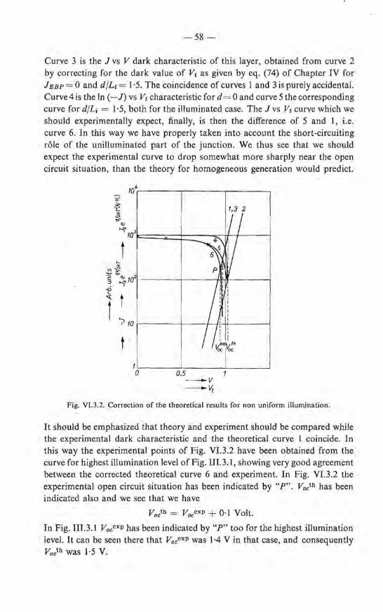
-58-
Curve 3 is the J vs V <lark characteristic of this layer, obtained from curve 2 by correcting for the dark value of Vi as given by eq. (74) of Chapter IV for J EBP = 0 and d /Lt = l · 5. The coincidence of curves 1 and 3 is purely accidental. Curve 4 is the In (-J) vs Vt characteristic ford = 0 and curve 5 the corresponding curve for d/Li = l ·5, both for the illuminated case. The J vs Vt curve which we should experimentally expect, finally, is then the difference of 5 and l, i.e. curve 6. In this way we have properly taken into account the short-circuiting röle of the unillurninated part of the junction. We thus see that we should expect the experimental curve to drop somewhat more sharply near the open circuit situation, than the theory for homogeneous generation would predict.
104-,-------.-------.------,
1,3 2
.., Il>-{::
~ ~Il> 1021------+----l-,lH't------t ;:, ~
.Q
~ t î .... 10 i--- - - -t-----1'--f-'-++-- ----t
t 1~---~----'--------' 0 0.5
-v -Vi
Fig. Vl.3.2. Correction of the theoretica! results for non uniform illumination.
It should be emphasized that theory and experiment should be compared while the experimental dark characteristic and the theoretica! curve 1 coincide. In this way the experimental points of Fig. VI.3.2 have been obtained from the curve for highest illumination level ofFig. III.3.1, showing very good agreement between the corrected theoretica! curve 6 and experiment. In Fig. VI.3.2 the experimental open circuit situation has been indicated by "P". V0 cth has been indicated also and we see that we have
Vocth = Vocexp + O·l Volt.
Jn Fig. III.3.1 V 0 cexp has been indicated by "P" too for the highest illumination level. It can be seen there that V0 cexp was l ·4 Vin that case, and consequently V0 /h was l ·5 V.

-59-
It should be noted (see Fig. VI.3.3) that for any point on curve 6 of Fig. Vl.3.2 the voltage drop V over the barriers in the illuminated part of the junction is obtained by first finding the point on curve 5 which corresponds to the same total voltage Vt. This point gives the current through the illuminated part of the junction. The point on curve 4 which corresponds to this current gives V, as has been mentioned in Chapter IV.
Strictly spoken the assumption of one dimensional geometry has been violated in this section. The error introduced will , however, be negligible as long as the length of the intrinsic region is small compared with the penetration depth of the illumination. Later on this will be shown to be true.
ln(-J)
î 103
~4 ~
102 ' 1
' 1 ' 1
: 1
l4 v
10
o.sv
-v -vt
Fig. VI.3.3. Derivation of V from Vi in the case of non uniform illumination.
VI.4 Quantitative analysis of the forward characteristics and of the photovoltaic effect
VI.4.1 Junctions prepared from recrystallized SiC
VI.4.l.1. The dark characteristics
For two reasons the <lark characteristics of these samples may be considered to give evidence for a p-i-n structure: 1. For a p-i-n structure one expects for Vi > 0 the In J vs Vi curves in the
dark to have a slope of q/2kT (see Section IV.7). Such slopes were experimentally found in the steep part of the curves, in many samples.
-60 -
2. According to eqs. (74) and (61) of Chapter IV for Jesp = 0, extrapolation of this steep part to zero voltage should yield the quantity:
Is = Is exp [-sinh (d/Lt) gd (d/Li)]. (3)
Is should therefore have the same temperature dependence as Is. Apart from possible deviations due to the temperature dependence of K tbis is in principle the temperature dependence of nt (eq. (49) of Chapter IV). Indeed an activation energy of l ·4 eV, which is equal to half the bandgap of 6H-SiC was found.
According to eqs. (6b), (16), (23) and (49) of Chapter IV, I s is given by the relation
(4)
By ignoring the exponential in (3) a lower limit of Is can be obtained. Under the assumption that the current is homogeneously distributed over the junction area (0.002 cm 2) we thus find from Fig. IIl.3.1 :
Is ;:::. 5 X I0-19 A cm-2.
Remembering that in (4) we have
and taking D = (2KDnDp/KDn + Dp)
Dn = 2·5 cm2 sec-1
(Dn/Dp) = K- 1 ~ 5
~ ~ 5 x 10- 4 cm- 3
we obtain from (1), (4) and (5):
Li ~ J0-4 cm or:
VTnFpi ~ 4 X 10-s sec.
(5)
(6)
(7)
(8)
(9)
(10)
( 11)
The values which are given for the various constants in eqs. (7) through (Il) are all reasonable for 6H-SiC 1).
VI.4.1.2 The photovoltaic effect
As was noted already in Section Vl.2 a comparison of the sbape of the experimental curves for the photovoltaic effect (Fig. III.3.1) with the theoretica! curves for the injection case (i.e. Fig. IV.8.2) suggests that we have :
d/L;, ~ 1·5.
From Fig. IV.8.3 we see that tbis would imply that the exponential in (3) is about 10- 1 . We thus would obtain a value of I s which is 10 times the lower limit given in (5) i.e.
Is = 5 X 10- 1s A cm- 2. (12)

-61-
Accordingly we would have:
Lt ~ 10-s cm (13) and
VTntTpt ~ 4 X 10⁻¹⁰ sec. (14)
These values are still reasönable 2). In Section II.2.3 it has been mentioned that the light source which was used for the photovoltaic effect caused a photon flux of F ~ 1016 photons cm- 2 sec-1 at the surface of the sample. When the
sample has a width d we have according to eq. (57) of Chapter IV the following relation between this flux and J EBP
qF [Ln +Lp + 2Lt tanh (d/Lt)] d = lEBP· (15)
From a comparison of Figs. 111.3.1 and IV.8.2 we obtain for the highest illumination level (which corresponds to the füll flux):
lEBP ~ 2 x 10-s A. (16)
With d = 0.1 cm eq. ( 15) then yields
Ln +Lp+ 2Lt tanh (d/Lt) ~ 10-4 cm. (17)
The inequality sign results from the fact that no losses due tq reflection and to a possible absorption in some ineffective surface layer were taken intö account. Eq. ( 17) shows that Ln or Lp or both are much larger than Lt as given by ( 13). Therefore we conclude that Lt « Ln + Lp, in accordance with the condition under which injection prevails over photoconductivity in the i-region (see Section IV.8). From eq. (61) of Chapter IV we obtain furthermore:
ls exp (qVocth/2kT) = lEBP (19)
and therefore, using eqs (49) and (55b) of Chapter IV:
nt exp(qVoctb/2kT) = [g(Ln + Lp)/2Lt]VTntTpt + gVTntTpt. (20)
This gives with (17) and (13):
(21)
By comparison of the curve for highest illumination level of Fig. III.3.1 with Fig. Vl.3.2 it can be seen that for this level we always had
V ~ V0éh - 0· 12 Volt. (22)
Substitution of (22) in (21) yields :
nt exp (qV/2kT) ~ ! gVTntTp'·

-62-
In view of the fact that losses due to reflection of light and due to absorption in ineffective surface layers have not been taken into account it thus seems reasonable to conclude that for the highest illumination level the condition
(23)
was fulfilled, i.e. that in the intrinsic region the injection prevailed over photoconductivity. We can now see that (23) must have been fulfilled also in the case of lower illumination levels: Due to the fact that the curves for different illumination levels transform into each other under translation in a direction with slope q/2kT, the left-hand member of (23) is proportional to the light intensity when for the various light intensities Vis taken to be the relevant open circuit voltage minus a positive constant. Therefore both members of (23) are proportional to the light intensity and (23) remains valid.
We have thus seen in this subsection that the suggested connection between the experimental results and the simple theory for the injection case of the photovoltaic effect seems to be consistent in the case of junctions prepared from recrystallized SiC. It remains to be shown that the various assumptions which have been made in the development of the theory are realistic. This will be done in the next sub-subsection.
VI.4.1.3 Justification of the assumptions, made in the theory
In Section Vl.3 we found for the case of highest illumination level V0cth = 1 ·5 Volt. Consequently we see from eq ( 64) of Chapter IV and from eqs (23), (22), (10), (8) .and (2) that under the highest illumination levels we had:
n ::'.: ni if; exp (qV/2kT) ~ 2·5 x JOS cm-3
p = K- 1 n ::'.: 1·25 x 1Q9 cm-3.
(24)
(25)
Therefore at the lowest illumination level used, (which was according to Fig. III.3.1 about a factor of thirty lower than the highest illumination level) we have:
n ::'.: 8 x 106 cm-3
p ::'.: 4 x 101 cm- 3.
(26)
(27)
These results will serve as an argument for the validity of some of our assumptions about the i-region:
(a) In all calculations nt was neglected in comparison with n and p in the i-region, which is in retrospect fully permitted by (26) and (27).
(b) In the i-region a constant lifetime was assumed, independent of injection level. This can be shown to be probably correct using the information given in (26) and (27), by considering the expression for the recombination rate via
-63-
recombination centres as derived by Shockley and Read 3) *):
np- nt2 r(n,p) = --------
Tpo(n + ni) + Tno (p + p1) (28)
According to (26) and (27), nt2 can be neglected in comparison with np. Furthermore n1 and p1 can be neglected when the centre lies sufficiently close to the middle of the forbidden energy gap. A simple calculation along conventional lines shows that in our case the condition for Er is:
IEr- Etl < 0·65 eV.
For an efficient recombination centre this is not a very severe restriction. Thus (28) reduces to:
r(n,p) = K-lnj(Tpo + K-1Tno) yielding constant lifetimes
(29)
(c) The existence of a constant trapping parameter K, defined by n = KP can now also be shown to be realistic. According to Shockley and Read 3) we can, under steady state conditions, write fora real trap centre, e.g. fora donor which has thermal communication with the conduction band only:
(30) From (30) we derive
ftd 0 - ftd = Llftd = [n2(n-no)/(n+n2)(no+n2)]. (31)
In our case it has been shown already that n » n0 , and when the centre lies more than a few kT from the middle of the bandgap, we have for intrinsic material n2 » n0 • Therefore (31) reduces to:
For an acceptor centre we obtain under analogous conditions:
Llfta = p/(p +Pa).
Equations (32a) and (32b) show that as long as
n « n2 and p « p2
(32a)
(32b)
(33)
the change of the fractional occupation of traps is proportional to the injected density .of the appropriate carrier.
*) Direct recombination need not be taken into account, since W. J. Choyke and L. Patrick 4) have shown the band-band transition to be indirect in 6H-SiC. Therefore the process of band-band recombination is expected to be a highly improbable process (See ref 1 of Ch III). According to an equation given by Rose 6) a concentration of ,.._,1Q23 carriers would be needed in. SiC to reduce the lifetime for this process below 10- 10 sec.

-64-
The highest injection levels during our experiment were obtained in the open circuit situation under the highest illumination. As has been noted already, Vocth in this case was 1·5 eV, giving rise to carrier concentrations.
n R::! 2·5 x 109 cm-3 p R::! 1·25x1010 cm-3
according to the first equation (24). Therefore the proportionality between the concentrations of free and trapped injected carriers holds for:
n2»2·5 x 109 cm-3 p2 » l ·25 x 1010 cm-3. (34)
From (34) the upper limit of the permissible level depth turns out to be 0·6 eV for both donors and acceptors.
For all intents and purposes then, we may permissibly write ntr = Knn and Ptr = Kpp, where Kn and Kp are constants. It bas been shown (see Section IV.2) that this is a sufficient condition for the introduction of the trapping parameter K which has been used throughout this Chapter and Chapter IV.
(d) It bas been assumed that the space charge regions are sufficiently narrow to justify a treatment of the i-region on the assumption of space charge neutrality. As is well known the width of these regions is indicated by the DebyeHückel length, which is defined by:
Lnn = (t:ot:rkT/q2N)t (35)
where N is the total concentration of charge-carriers present, both trapped and untrapped 6). The i-region can be assumed to be essentially neutra! when Lnn < d. In our case where d/Lt R::! l ·5 and L R::! 10- 5 cm we therefore need a Debye-Hückel length of less than 10-5 cm.
Eq. (35) shows that the concentration of charge carriers, trapped or un- · trapped, should be at least 1015 cm-3 to achieve this.
On one side of the i-region this concentration will be composed mainly of trapped electrons. Therefore it must be required, according to (32) and (33), that during the experiments the relation
(N na n/n2) :: 1015 cm- 3 (36) was fulfilled.
Using (34) we obtain from (35) the condition
2·5 x 1024 Nna:: cm-3•
n (37)
Substitution of the lowest value of n which occurred during the experiments, i.e. of (26) then yields:
Nna:: 0·25 x 1018 cm-3. (38)
C!early, on the other side of the i-region a similar amount of <leep acceptors is needed. Such concentrations of <leep centers are quite well possible 7) though because of the small dimensions of the i-region their presence cannot be

-65-
experimentally verified by known methods. The results of the above considerations have partly been summarized in Fig. VI.4.1.
Ec77T77777rr7"7i'7"li'77"7'"1>-7&-~'7-r7} >f018traps cm-3
Ec-0.6 eV'-'-~'-"-"-'--''-"-"'-"-"1~'-"--''-"-"'"""'-.....,_.4'-""'-~+9.65 e V"'"'"'""'""""""~~"'"'""'~'*"""
Ei =fc-1.43eV ~~~~~~ffl~~~~~} Recombinaficri een tres
E;-0.65 el/'""' -'-"->...>...>..:~P-'1->...:W."""-'"""-'~~'"""-'~>..::.:. . Ev+0.6 eV 'l"/, }
/// >1d8trops cm-3 Ev = Ec-2.86 e V ~'-"-1'~""""+~<-'-'~-<....L.""-'--'-'-'~-+-'-""
Fig. VI.4.1. Energy level diagram for the i-region, as derived in this work. The arrows indicate the transitions which have been taken into account.
With the information obtained so far a number of assumptions about the n- and p-region can be discussed a!so:
(a) It has been shown in Chapter IV that the injection-case can only be treated in simple form, i.e. with voltage independent fesp for
qglLn - Lpl « ls exp (qV/2kT). (39)
Comparison of Figs. Ill.3.1 and VI.4.2 shows that we have always worked under the éondition
0,1 lEsP ::;;;Js exp (qV/2kT) i.e. (for Li « Ln + Lp):
0· 1 qg(Ln + Lp) ::::;; ls exp (q V/2kT).
We thus see that (39) is fulfilled if
ILn - Lpl « O· l (Ln + Lp).
(40)
(41)
We thus expect the analysis to be substantially correct when Ln and L p do not differ by more than about 20 %. This is of course a rather severe restriction.
(b) In the course of the calculations terms containing minority carrier concentrations, i.e.:
qK-lpn (Lp/Tp) exp (2qVr/kT)
qKnp (Ln/Tn) exp (2q Vi/kT)
have been neglected in comparison with terms such as:
2qnt (Lt/V TniTpi) tgh (d/Lt) exp (q V/2kT) cosh o
(42)
(43)
(see e.g. eqs. (Al2), (Al3) and (A14) of Appendix A). These quantities can now be numerically compared. We first note from eq. (34) of Chapter IV and (8) that under our previous assumptions we have:
(44)
-66-
Therefore we are certainly allowed to neglect the quantities (42) in comparison with the quantity (43) when:
t exp (qV/kT) ( ( ( r11, exp (qV/2kT) (45)
where t denotes a minority carrier concentration (i.e. np or pn) and where the sign ( ( ( means: "many orders of magnitude smaller than". When ( 45) is shown to be correct under our experimental conditions we need not bother about differences in diffusion constants and lifetimes nor about the exact value of K ,
since it would physically have been sufficient to prove (45) using the sign «. Eq. (45) is most likely to be violated for high values of V. Therefore we shall consider (45) for the highest value of Vwhich has been used, i.e. V = 1 ·5 Volt.
Substitution into ( 45) then leads to:
t ( (( 5 x 10-17 cm-3.
Or, for the majority carrier concentration:
(46)
At first sight this condition does not seem to be very severe. A crude calculation showed however that, although we do not have enough information to state that (46) is violated,it is not necessarily ful:filled either. We shall, for the sake of argument, assume however that ( 46) and therefore ( 45) was valid du ring our experiments.
(c) An immediate consequence of (45) is:
t exp (qV/kT) ( ( ( (nt 2/t). (47)
Eq. ( 47) states that the concentration of injected minority carriers in the p- and n-regions is much smaller than the equilibrium majority carrier concentration, which may be regarded as streng although not entirely conclusive evidence for the constancy of Ln and Lp S).
We thus see that all assumptions which have been made can be regarded as being justified, with the exception of eq (1). For this assumption we cannot provide a physical basis. lt bas on the ether hand been shown in Section IV.9 that serious deviations from the predictions of the simplified theory need not occur when (1) is not fulfilled. We therefore conclude that probably the interpretation of the experimental results is in principle correct hitherto.
VI.4.2. Junctions prepared from technica! grade SiC
The experimental results on junctions prepared from technica! grade SiC do not lend themselves to detailed analysis, since their appearance as far as the photovoltaic effect is concerned, is not very specific (Fig. III.3.2). As already mentioned in Section III.1 their <lark characteristics are very similar to those of samples which have been prepared from recrystallized SiC. The photovoltaic

-67-
effect might be interpreted by assuming that in the i-region the injection dominates over the photoconductivity while d/Lt < 1 (Fig. IV.8.2) as well as by assuming photoconductivity to be predominant (Fig. IV.8.1 ). Due to the small values of leBP a decision cannot be made.
VI.5 Forward characteristics with slope < q/2kT
It bas been mentioned in Chapter UI that many samples only displayed a slope of q/2kT in their forward characteristics at higher temperatures, while at Iower temperatures the slope was somewhat smaller than q/2kT. At the same time Is did not show an activation energy in the latter temperature region.
Since most parallel transport mechanisms tend to redtice the slope of the In l vs Vt curves in the dark it might very well be that for lower temperatures some parallel current path plays a significant róle. In fact such a parallel transport mechanism was observed in many samples originating from a somewhat anomalous preparation run and an analysis was performed in the case of one of these (Section 111.2). Furhtermore we have seen from the p-n luminescence (Chapter V) that at very high currents the distribution of current density over the junction area is inhomogeneous. Whether these three aspects of the behaviour of the junctions are related is not clear at the moment.
VI.6 Anomalous activation energies
As has been mentioned in Chapter UI, in samples from one particular preparation run, [8 showed an activation energy of l ·55 e V. Many samples out of this run showed a second component in their forward <lark characteristics. In one particular sample we could determine the corresponding activation energy, for which a value of 1 ·2 eV was found (Section IIl.3). These activation energies are remarkably close to half the value of the forbidden energy-gaps of JC-SiC and 4H-SiC (see Chapter I). No conclusive evidence has been found, however, to correlate these results with the occu_rrence of JC-SiC and 4H-SiC in the sample 9). In this preparation run the "foot" was very dominant. Therefore our analysis of the photovoltaic effect could not yield additional information in this case.
VI. 7 Electron temperature
One additional remark concerning the temperature of the carriers should be made: lt bas been shown that under illumin~tion the voltage drop over the i-region can become of the order of 1 Volt in the short-circuit situation (see e.g. Fig. VI.4.2). With d/Li = 1 ·5 and Li = 10-5 cm this would give an electric field of 105 V cm-1, and the electrons would therefore attain velocities of 107 cm/sec. (their mobility being ""100 cm2 sec- 1 v - 1). This means that the electrons would tend. to become hot, and therefore the Boltzmann equilibria which provided the boundary conditions for the treatment in Chapter IV, are

-68-
possibly not entirely correct under these conditions. For this reason the results of the theory should be regarded with some caution.
VI.8 Concluding remarks
Although it is possible to obtain theoretica! curves for the genera! case and to use these for the best possible determination of the various parameter values, this has not been attempted in the present stage in view of the complexity of the numerical evaluations. Furthermore, it has been shown in the last two Chapters that the current density is in our samples inhomogeneously distributed over the junction area. This circumstance introduces uncertainties in the corrections for non uniform illumination, and therefore comparison with a cumbersome and detailed theory does not seem worthwhile. Moreover a good fit between the simplified theory of Section IV.8 and the experiments was obtained in this
Chapter, using a reasonable value of Vr niTpi, and correcting in a reasonable way for non uniform illumination. It should furthermore be noted that the value obtained for d/Lt from the shape of the ln(-J) vs Vi curves under il
lumination is independant of the value of Vr n tTpi· In addition it has been shown (Sections IV.8 and IV.9) that d/Lt enters the theory in a very critical way. Therefore the value which was found is probably correct.
REFERENCES:
1) H. J. van D a al, W. F. Knippen berg and J . D. Wasscher, to be published. 2) L. Patrick and W. J. Choyke, Proc. SiC Conf. 281-305, 1960. S) W. Shockley and W. T. Read, Phys. Rev. 87, 835-842, 1952. 4) W. J. Choyke and L. Patrick, Proc. SiC Conf. 307-311, 1960. 5) A. Rose, Proceedings of the Photoconductivity Conference 1954. John Wiley and Sons
Ine. New York 1960, p. 3-48. 6) A. Rose, H.P.A. 29, 199-201, 1956. 7) W. F. Knippen berg to be published. 8) F. v.d. M a esen and C.A. A. J. Greebe, to be published. 9) C. A. A. J. Greebe and W. J. Knippen berg, Philips Res. Repts 16, 389-398, 1961.

CHAPTER VII
CONCLUSIONS
It has been shown in this thesis that the p-n structures in SiC which were prepared using the Lely process, have a p-i-n like structure, as one would expect due to the high bandgap of this substance. Furthermore an explanation of the relative dimensions of the n- and p-regions has been suggested. Evidence has been presented which indicates that the current density is often inhomogeneously distributed over the junction area at high current densities (by analysis of the spectra! distribution of the p-n luminescence) as wel! as at low current densities (by analysis of the forward characteristics). As should be expected the experimental evidence strongly suggests that in the case of 6H-SiC the theory of van Roosbroeck and Shockley for band-band transitions can be applied. Analysis of the photovoltaic effect and of the forward cbaracteristics in the dark indicates that the deviations from exponential behaviour at low current densities of the Jatter are due to an electrically parallel, i.e. short-circuiting mechanis1n which is relatively insensitive to illumination.
In addition the theory of Herlet and Spenke for p-i-n junctions has been extended. For a relatively simple case explicit equations for the photovoltaic effect of a p-i-n junction have been obtained. It has been shown also that under illumination the modtilation of the resistivity of the intrinsic regiou of a p-i-n structure. can be due to photoconductivity as well as to injection. These two possibilities give rise to distinctly different kinds of behaviour of the structure.
The behaviour in darkness as well as under illumination of the junctions · studied in this work appears to be consistent with the hitherto obtained theoretica! results.

-70-
APPENDIX A
The evaluation of the concentration of charge carriers and of the total current from the solutions of the continuity equations
Substitution of (31) in (21) yields *):
C1 exp (d/Lt) + C2 exp (-d/Lt) + g-rni = nt exp (qVr/kT). (AI)
C1 exp (-d/Li) + C2 exp (d/Lt) + g-rni = Knt exp (q Vi/kT). (A2)
Adding (Al) and (A2) gives:
2(C2 + C1) cosh (d/Lt) + 2g-rnt = nt[K exp (qVi/kT) + exp (qVr/kT)] = = 2n, vÇ exp ( q V/2kT) cosh S ( A3)
where V = Vi + Vr
S = (q/2kT)( Vz - Vr) + -! In K.
(A3) can be rewritten as:
(A4)
(AS)
C1 + C2 = [nivÇ exp (qV/2kT) cosh S- g-rni]/cosb (d/Lï). (A6)
Analogeously we obtain by subtraction of (A2) from (Al):
C2 - C1 = [n,vÇ exp (qV/2kT) sinh S]/sinh (d/Lt). (A7)
Substitution of (A6) and (A7) in (21) can easily be performed when (21) is rewritten as:
One thus arrives at eq. (37) for the electron concentration in the i-region:
n = g-rnt 1- + nt VK exp (qV/2kT) cash S--- -[ cash (x/Lt)] 11 cosh (x/Lt)
cosh (d/Lt) cash (d/Lt)
11 sinh (x/Lt) - nt v K exp (qV/2kT) sinh S · .
sinh (d/Lt) (A9)
This equation is valid only for n » nt, since (21) bas been derived under this assumption. The consistency of the treatment is easily seen by noting that the absolute value of the second term of (A9) is always larger than the absolute value of the third term. The first and second terms of (A9) are positive. Therefore n can be made indefinitely large by large g and V.
From (26) and (31b) we obtain for the case that LJp » pn:
(AIO)
*) All numbers between brackets refer to the equations of Chapter IV.

-71-
Similarly (All)
When use is made of (6b), substitution of (A6), (AIO) and (All) into the expressions (24), (27) and (29) for J(t), J<n> and J<Pl yields:
J(t) = 2qnt(LtJVTniTpt) tanh (d/Lt) exp (qV/2kT)cosh o-2qgLt tanh (d/Lt) (Al2)
j(n) = qK-1pn (Lp/Tp) exp 2q Vrf kT)- qgLp
j(P) = q1mp (Ln/Tn) exp (2qVifkT)- qgLn.
(A13)
(Al4)
Addition of these expressions gives the toiftl current, in which the terms containing the minority carrier concentrations np and Pn can be neglected in the case of semiconductors with a high bandgap (see Chapter VI). The result is eq. (35).
The condition that in the steady state the two harriers must carry the same current
Jn(-d) + Jp(-d) = Jn(+ d) + Jp(+d) (Al5)
yields an expression for o as a function of Vi + Vr. In Al5 Jn(- d) and Jp( + d) are equal to J<Pl and J<n> respectively as given by (A13) and (Al4). When dn/dx is taken from (21), we can obtain Jp(-d) and Jn( +d) from (13) and (14):
Jn( +d) = qD[(C1/Lt) exp (d/Lt)- (C2/Lt) exp (-d/Lt)] + + µnJ/(µ n + K-1µp) (A16)
Jp(-d) = - qD[(C1/Lt) exp (-d/Lt) - (C2/Lt) exp (d/Lt)] + + K- 1µpJ/(µn + K-1µp. (Al?)
When again terms containingpn and np are neglected, substitution of(A13), (Al4), (A16) and (Al?) in (A15) gives:
(Al8)
With (A7) and with the relation Tnt = KTpt (eq. 6b) we obtain from (A18) the relation for o, mentioned in the text of Chapter IV as eq. (36).
APPENDIX B
Proof of the monotonous dependence of V on Vt for µnn = µpp
In Section IV.8 we used in the range Vt :::;; V0cth the relation
dV - ::::::: 0 d Vt ""'
(Bl)

-72-
for the explicit evaluation of the photovoltaic effect under the assumption that in the i-region µnn and µpp are equal.
In order to prove (Bl) it must first be shown that for Vi ~ V0 cth we always . have
J~O.
Suppose that in this range we have J > 0. According to eq. (61) of Chapter IV this means that V > V0 cth since for V = V0 cth we have J = 0. However, when V > V0cth and Vi ~ V0cth we must conclude that Vi = Vi - V is negative and hence J < 0, in contrast to the assumption J > 0. When we now suppose
dV that - < 0, we must conclude from the relation Vi = V + Vi that
dVi dVi dVi
1- - < 0 or - > 1. Since Vi = 0 when Vi = V0 cth we thus are dVt dVt
led to the conclusion that for Vt ~ V0cth we have - Vi > V0cth - Vi which is identical to V > V0 cth. This would imply J > 0. It has however been shown already that J ~ 0.
From this contradiction it is seen that (Bl) is valid for Vi ~ V0 cth.

-73-
SAMENVATTING
P-n overgangen in SiC, die met gebruikmaking van het Lely procédé zijn gegroeid bleken een p-i-n structuur te hebben. Dit is overeenkomstig de verwachting, aangezien SiC een hoge "bandgap" heeft. De afmetingen van het p- en het n-gebied hebben veelal een merkwaardige verhouding en een verklaring hiervoor wordt voorgesteld. Er zijn aanwijzingen gevonden voor een inhomogene verdeling van de stroomdichtheid over de p-n overgang, zowel bij hoge stroomsterkte (door een analyse van de spectrale verdeling van de p-n luminescentie) als bij lage stroomsterkte (door een analyse van de stroomspanningskarakteristieken). Zoals te verwachten viel kan de theorie van van Roosbroeck en Shockley voor band-band overgangen in het geval van SiC worden toegepast.
Uit een analyse van het photo-voltaisch effect en van de stroom-spanningskarakteristieken in donker blijkt, dat het kortsluitmechanisme dat bij lage stromen de laatste overheerst, opgevat kan worden als een (electrisch zuiver parallel) lek dat relatief ongevoelig voor licht is. De theorie van Herlet en Spenke voor p-i-n overgangen werd uitgebreid. Voor een bijzonder geval werden expliciete vergelijkingen verkregen voor het photo-voltaisch effect van zulke overgangen. Er werd aangetoond dat onder belichting de modulatie van de weerstand van het intrinsieke gebied door photogeleiding zowel als door injectie kan geschieden. Deze twee mogelijkheden geven aanleiding tot zeer verschillende verschijnselen. Zowel onder belichting als in donker blijken de overgangen zich in overeenstemming met de theorie te gedragen, voorzover deze op het ogenblik quantitatief is uitgewerkt.

-74-
ACKNOWLEDGEMENT
The investigations described in this thesis have been carried out in continuous and close cooperation with Mr. W. F. Knippenberg who studied the subject from amore chemica! point of view. This pleasant association is gratefully acknowledged.
lt is a pleasure to express here my indebtedness to the directors of the Philips Research Laboratories for their kind permission to publish the work in this form and to all those who have in any way contributed to it.
Special thanks are due to: Ir. F. H. Stieltjes for many instructive and inspiring discussions, Dr. H. J. Vink for his unfailing interest and support, Dr. F. van der Maesen, Mr. P. C. Newman and Dr. F. N. Hooge for heplful comments, and Mr. J. J. A. M. Vrakking for his skilful help during the measurements.

-75-
Curriculum vitae:
1949
1956
1957-1959
Eindexamen H. B. s.~B (te Almelo)
Dotoraal Examen Experimentele Natuurkunde (te Groningen)
Militaire dienst
Vanaf 1959: Werkzaam in Natuurkundig Laboratorium van de N.V. Philips' Gloeilampenfabrieken (te Eindhoven)

a
a (v) D Dn Dp 2d d d 13
E EA En Eg
Eis
Et Er LlE B
Bo Br
F ftd ftdO Llftd LJfta g(p,n);g I I (v) Io (v) Iph
Is
J
JEPB
Jd ln lp ls j(i)
j(n)
-76-
LIST OF SYMBOLS
Absorption coefficient of light idem Ambipolar diffusion constant Diffusion constant of electrons Diffusion constant of holes Thickness of intrinsic region crystal thickness crystal width q/2kT (Vi- Vr) + !lnK Electric field strength Level depth of acceptor idem of donor band gap Activation energy of Is Middle of the forbidden energy gap Energy level of recombination centre Electric field strength associated with the Dember field Dielectric constant idem for vacuum idem, relative Photon flux Occupation ratio of electron trap idem in thermal equilibrium ftd- ftdO Analogous to LJftd for hole trap Generation rate Measured current in darkness Spectra} distribution of p-n lurninescence as detected idem as emitted Photocurrent of p-n junction Extrapolation of steep part of experimental <lark characteristic to zero voltage Current through a p-i-n structure Equivalent Bias Photocurrent Dark current Electron current Hole current Saturation current Current due to recombination in the i-region idem, n-region

j(P)
k
K
LDH
Li Ln Lp µn
µp
NA ND
NDd
LJN n
p Pn po p3 LJp
Ptr q r (p, n); r
Gp
T To t
· Tni
T p j
Tp
v
idem, p-region Boltzmanns constant LJn
LJp
-77-
Debye-Hückel length Diffusion length in i-region idem p-region idem n-region Mobility of electrons Mobility of holes Acceptor concentration Donor concentration Concentration of deep traps Difference between donor concentrations in the n- and p-regions Electron concentration Intrinsic concentration Electron concentration in p-region (equilibrium) Electron concentration in equilibrium Ratio of capture- and emission constant for electrons of recombination centre. idem for electron trap n- no Concentration of trapped electrons Hole concentration Hole concentration in n-region (equilibrium) Hole concentration in equilibrium Ratio of capture and emission constant for holes of hole trap p-po Concentration of trapped holes Electric charge of an electron Recombination rate Specific conductivity of n-region idem p-region Absolute temperature Characteristic temperature minority carrier concentration Lifetime of electrons and holes in i-region, case of no trapping Lifetime of electrons in i-region Lifetime of holes in i-region Lifetime of electrons in p-region Lifetime of holes in n-region Total voltage drop over bärrier(s)

Vt Vi.Q Vw Vt.Q Vt.Q Vz Vr Vocth
Vocezp
Vt
-78-
Voltage drop over i-region Ohmic voltage drop over the i-region Voltage drop over i-region due to Dember field Upper limit of Vi.Q Lower limit of Vi.Q Voltage drop over the p-i harrier idem i-n harrier Theoretica! open circuit voltage Experimental open circuit voltage
Vz+ Vr + Vi

STELLINGEN
I
De nomenclatuur die veelal gebruikt wordt om de bij injectie en extractie in halfgeleiders optredende typen van ruimtelijke verdelingen van ladingsdragers aan te duiden, is misleidend.
II
Twee van de vier karakteristieke lengtes waarvan men zich vaak bedient bij de volledige beschrijving van kleine injecties en extracties in halfgeleiders, kunnen onder bepaalde omstandigheden een complexe waarde aannemen.
III
In halfgeleiders bestaat er met betrekking tot het verschijnsel dat bekend staat als "trapping", een dualiteit tussen bepaalde ruimteladings- en diffusie-recombinatie effecten.
IV
De 4e-machtsvergelijking waartoe, in stationnaire toestand, kleine afwijkingen van de evenwichtsconcentraties van electronen en gaten in halfgeleiders aanleiding geven, kan op eenvoudige en overzichtelijke wijze grafisch worden opgelost, door nieuwe veranderlijken in te voeren.
C. A. A. J. Greebe en F . v. d. Maesen Philips Res. Reps. (in voorbereiding).
v
Tegen de beschouwingen van M.R. Boite over injecties en extracties in halfgeleiders zijn, afgezien van enkele rekenfouten, bedenkingen aan te voeren. In het bijzonder schept zijn behandeling als le orde probleem van een extractie die constant is in de tijd, verwarring wat betreft het aantal op te leggen randvoorwaarden.
M. R. Boite, Revue H. F. ,IV, 151 -156, 1959.
VI
R. A. Smith behandelt in zijn boek "Semiconductors" de thermoëlectrische kracht op principieel onjuiste wijze.
R. A. Smith, "Semiconductors" Cambridge University Press 1959, p. 170-172

VII
W. Klose discussieert de invloed van een temperatuur gradient op het gedrag van een p-n overgang op onjuiste wijze.
W. Klose, Ann. d. Phys. 6, 25-30, 1960.
VIII
R. N. Hall gebruikt in zijn analyse van het gedrag van p-i-n overgangen een foutieve randvoorwaarde.
R. N. Hall Proc. l. R. E., 40, 1512-1519, 1952.
IX
De grote invloed van de publieke smaak op de programma's van symphonieconcerten leidt tot onverantwoorde uitvoeringspraktijken.
x In tegenstelling tot een veel verbreide opvatting zijn de vroegere symphonieën van Franz Schubert van grote muzikale waarde.
XI
De studie van de Vaste Stof aan de Nederlandse Universiteiten en Technische Hogescholen dient bij voorkeur te geschieden in instituten waar physici en chemici op voet van gelijkheid en in nauw contact kunnen samenwerken.