Embed Size (px)
Citation preview

©2010-2017 Peregrine Semiconductor Corp. All rights reserved.
Page 1 of 12
Document No. DOC-77985-2 | www.psemi.com
Features
HaRP™ technology enhanced
Fast settling time
Eliminates gate and phase lag
No drift in insertion loss and phase
High linearity: 58 dBm IIP3
Low insertion loss: 0.8 dB @ 3 GHz,
1.0 dB @ 6 GHz and 1.2 dB @ 8 GHz
High isolation: 45 dB @ 3 GHz,
39 dB @ 6 GHz and 31 dB @ 8 GHz
Maximum power handling: 30 dBm @
8 GHz
High ESD tolerance of 2 kV HBM on
RFC and 1 kV HBM on all other pins
PE42540
UltraCMOS® SP4T RF Switch
10 Hz–8 GHz
The PE42540 is a HaRP™ technology-enhanced absorptive SP4T RF switch developed on UltraCMOS® process technology. This switch is designed specifically to support the requirements of the test equipment and ATE market. It comprises four symmetric RF ports and has very high isolation. An on-chip CMOS decode logic facilitates a two-pin low voltage CMOS control interface and an optional external VSS feature. High ESD tolerance and no blocking capacitor requirements make this the ultimate in integration and ruggedness. The PE42540 is manufactured on Peregrine’s UltraCMOS process, a patented variation of silicon-on-insulator (SOI) technology on a sapphire substrate, offering the performance of GaAs with the economy and integration of conventional CMOS.
Figure 1. Functional Diagram
RF4
RF1
RF3
CMOS Control/Driver and ESD
VDD V1
ESD
RF2
V2
ESD
50
ESD
50
ESD
50
ESD
50
VssEXT
RFC
Figure 2. Package Type
32-lead 5 × 5 mm LGA
Product Description
Product Specification
71-0067

Document No. DOC-77985-2 | UltraCMOS® RFIC Solutions
Page 2 of 12
©2010-2017 Peregrine Semiconductor Corp. All rights reserved.
PE42540 Product Specification
Table 1. Electrical Specifications @ +25°C, VDD = 3.3V, VSS_EXT = 0V (ZS = ZL = 50Ω )
Parameter Condition Min Typ Max Unit
Operating frequency 10 Hz1 8 GHz
RFC–RFX insertion loss
10 Hz–9 kHz
3000 MHz
6000 MHz
7500 MHz
8000 MHz
0.7
0.8
1.0
1.1
1.2
1.0
1.1
1.3
1.5
1.6
dB
dB
dB
dB
dB
RFX–RFX isolation
10 Hz–9 kHz
3000 MHz
6000 MHz
7500 MHz
8000 MHz
70
40
34
27
25
80
45
39
32
31
dB
dB
dB
dB
dB
RFC–RFX isolation
10 Hz–9 kHz
3000 MHz
6000 MHz
7500 MHz
8000 MHz
74
40
28
24
21
84
45
33
29
27
dB
dB
dB
dB
dB
Return loss (RFC to active port)
10 Hz–9 kHz
3000 MHz
6000 MHz
7500 MHz
8000 MHz
24
23
18
14
13
dB
dB
dB
dB
dB
Return loss (terminated port)
10 Hz–9 kHz
3000 MHz
6000 MHz
7500 MHz
8000 MHz
35
18
13
11
10
dB
dB
dB
dB
dB
Settling time 50% CTRL to 0.05 dB final value (–40 to +85 °C) rising edge
50% CTRL to 0.05 dB final value (–40 to +85 °C) falling edge
14
15
18
45
μs
μs
Switching time (TSW) 50% CTRL to 90% or 10% RF 5 8 μs
P1dB1 input 1 dB compression
point RFX–RFC All bands @ 1:1 VSWR, 100% duty cycle 31 33 dBm
Input IP3 8000 MHz 58 dBm
Input IP2 8000 MHz 100 dBm
Note 1: Maximum operating PIN (50Ω) is shown in Table 3. Please refer to Figure 4, Figure 5 and Figure 6 when operating the part at low frequency.

©2010-2017 Peregrine Semiconductor Corp. All rights reserved. Document No. DOC-77985-2 | www.psemi.com
PE42540
Page 3 of 12
Product Specification
Figure 3. Pin Configuration (Top View)
Pin # Pin Name Description
1, 3-6, 8,
9-12, 14-17,
19-22, 24-26,
28, 32
GND Ground
2 RF42 RF I/O
7 RF22 RF I/O
13 RFC2 RF common
18 RF12 RF I/O
23 RF32 RF I/O
27 VDD Supply
29 V1 Switch control input, CMOS logic level
30 V2 Switch control input, CMOS logic level
31 VSS_EXT1 External VSS negative voltage
Paddle GND Exposed solder pad: Ground for
proper operation
Table 2. Pin Descriptions
Notes: 1. Use VSS_EXT (pin 31, VSS_EXT = –VDD) to bypass and disable internal negative voltage generator. Connect VSS_EXT (pin 31) to GND (VSS_EXT = 0V) to enable internal negative voltage generator.
2. All RF pins must be DC blocked with an external series capacitor or held at 0 VDC.
Table 3. Operating Ranges
Parameter Min Typ Max Unit
Supply voltage, VDD 3.0 3.3 3.55 V
Negative power supply voltage1, VSS_EXT
–3.6 –3.3 –3.0 V
Negative supply current, Iss –10 –40 µA
Power supply current, IDD VDD = 3.3V, VSS_EXT = 0V, Temp = +85 °C
90 160 µA
Power supply current, IDD VDD = 3.6V, VSS_EXT used
50 µA
Control voltage high (V1, V2) 1.2 1.5 VDD V
Control voltage low (V1, V2) 0 0 0.4 V
Control current, ICTRL 1 µA
PIN thru path2 (50Ω, RF power in) 9 kHz – 1 GHz 1 GHz – 8 GHz (85 °C, VSS_EXT = –3.0V) (85 °C, VSS_EXT = 0.0V) (85 °C, VSS_EXT = –3.5V)
Fig. 4–6
30 30 28
27.5
dBm
Max power into termination (50Ω)
9 kHz ≤ 6 MHz2,3
6 MHz–8 GHz2,3
Fig. 4–6
20 dBm
Max power, hot switching (50Ω)
9 kHz ≤ 6 MHz2,3 6 MHz–8 GHz2,3
Fig. 4–6 20
dBm
Operating temperature range, TOP –40 +85 °C
Notes: 1. Applies only when external VSS power supply is used. Otherwise, VSS_EXT = 0. 2. 100% duty cycle (–40 to +85 °C, 1:1 VSWR). 3. Do not exceed 20 dBm.
8
7
6
5
4
3
2
1 24
23
22
21
20
19
18
17
32 31 30 29 28 27 26 25
161514131211109
Exposed Pad
GND
RF2
RF4
GND
GND
GND
GND
GND
GND
RF1
RF3
GND
GND
GND
GND
GND
GN
D
GN
D
GN
D
GN
D
GN
D
RF
C
GN
D
GN
D
GN
D
GN
D
VS
S_E
XT
V2
V1
GN
D
VD
D
GN
D
Pin 1 Dot
Marking

Document No. DOC-77985-2 | UltraCMOS® RFIC Solutions
Page 4 of 12
©2010-2017 Peregrine Semiconductor Corp. All rights reserved.
PE42540 Product Specification
Exceeding absolute maximum ratings may cause permanent damage. Operation should be restricted to the limits in the Operating Ranges table. Operation between operating range maximum and absolute maximum for extended periods may reduce reliability.
Electrostatic Discharge (ESD) Precautions
When handling this UltraCMOS device, observe the same precautions that you would use with other ESD-sensitive devices. Although this device contains circuitry to protect it from damage due to ESD, precautions should be taken to avoid exceeding the specified rating.
Latch-Up Immunity
Unlike conventional CMOS devices, UltraCMOS devices are immune to latch-up.
Switching Frequency
The PE42540 has a maximum 25 kHz switching rate when the internal negative voltage generator is used (pin 31 = GND). The rate at which the PE42540 can be switched is only limited to the switching time (Table 1) if an external negative supply is provided at (pin 31 = VSS_EXT).
Table 5. Truth Table
State V1 V2
RF1 on 0 0
RF2 on 1 0
RF3 on 0 1
RF4 on 1 1
Spurious Performance
The typical spurious performance of the PE42540 is –144 dBm when VSS_EXT = 0V (pin 31 = GND). If further improvement is desired, the internal negative voltage generator can be disabled by setting VSS_EXT = –VDD.
Moisture Sensitivity Level
The moisture sensitivity level rating for the PE42540 in the 32-lead 5 × 5 mm LGA package is MSL3.
Optional External Vss
For proper operation, the VSS_EXT pin must be grounded or tied to the Vss voltage specified in Table 3. When the VSS_EXT pin is grounded, FETs in the switch are biased with an internal voltage generator. For applications that require the lowest possible spur performance, VSS_EXT can be applied externally to bypass the internal negative voltage generator.
Table 4. Absolute Maximum Ratings
Parameter Min Max Unit
Maximum junction temperature +150 °C
Storage temperature range, TST –60 +150 °C
Supply voltage, VDD –0.3 4 V
Control voltage (V1, V2) 4 V
PIN thru path2 (50Ω, RF power in) 9 kHz – 1 GHz 1 GHz – 8 GHz (85 °C, VSS_EXT = –3.0V) (85 °C, VSS_EXT = 0.0V) (85 °C, VSS_EXT = –3.5V)
Fig. 4–6
30 30 28
27.5
dBm
Max power into termination (50Ω)
9 kHz ≤ 6 MHz1
6 MHz–8 GHz
Fig. 4–6
20
dBm
ESD voltage HBM2
RFC
All pins
2000
1000
V
V
ESD voltage CDM3, all pins 450 V
ESD voltage MM4, all pins 100 V
Notes: 1. Do not exceed 20 dBm. 2. Human body model (MIL-STD 883 Method 3015). 3. Charged device model (JEDEC JESD22–C101). 4. Machine model (JEDEC JESD22-A115-A).
©2010-2017 Peregrine Semiconductor Corp. All rights reserved. Document No. DOC-77985-2 | www.psemi.com
PE42540
Page 5 of 12
Product Specification
VDD VSS_EXT Minimum Peak
Voltage at RF Port
Maximum Peak
Voltage at RF Port
≥ 3.0 0.0 –0.2 1.2
3.0 –3.0 –0.6 1.6
3.3 –3.3 –0.3 1.3
3.5 –3.5 –0.1 1.1
3.6 –3.6 0.0 1.0
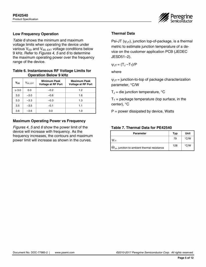
Low Frequency Operation
Table 6 shows the minimum and maximum voltage limits when operating the device under various VDD and VSS_EXT voltage conditions below 9 kHz. Refer to Figures 4, 5 and 6 to determine the maximum operating power over the frequency range of the device.
Maximum Operating Power vs Frequency
Figures 4, 5 and 6 show the power limit of the device will increase with frequency. As the frequency increases, the contours and maximum power limit will increase as shown in the curves.
Table 6. Instantaneous RF Voltage Limits for
Operation Below 9 kHz
Thermal Data
Psi-JT (JT), junction top-of-package, is a thermal
metric to estimate junction temperature of a de-
vice on the customer application PCB (JEDEC
JESD51–2).
JT = (TJ –TT)/P
where
JT = junction-to-top of package characterization
parameter, °C/W
TJ = die junction temperature, °C
TT = package temperature (top surface, in the
center), °C
P = power dissipated by device, Watts
Table 7. Thermal Data for PE42540
Parameter Typ Unit
JT 79 °C/W
JA, junction-to-ambient thermal resistance
128 °C/W

Document No. DOC-77985-2 | UltraCMOS® RFIC Solutions
Page 6 of 12
©2010-2017 Peregrine Semiconductor Corp. All rights reserved.
PE42540 Product Specification
-15
-10
-5
0
5
10
15
20
25
30
35
0 1 10 100 1,000 10,000 100,000 1,000,000
Inp
ut
Po
we
r (d
Bm
)
Frequency (kHz)
VssEXT = -3.0V, VDD = +3.0V
VssEXT = 0.0V, VDD ≥ +3.0V
VssEXT= -3.5V, VDD=+3.5V
-15
-10
-5
0
5
10
15
20
25
30
35
0 1 10 100 1,000 10,000 100,000 1,000,000
Inp
ut
Po
we
r (d
Bm
)
Frequency (kHz)
VssEXT = -3.0V, VDD = +3.0V
VssEXT = 0.0V, VDD ≥ +3.0V
VssEXT= -3.5V, VDD=+3.5V
-15
-10
-5
0
5
10
15
20
25
30
35
0 1 10 100 1,000 10,000 100,000 1,000,000
Inp
ut
Po
we
r (d
Bm
)
Frequency (kHz)
VssEXT = -3.0V, VDD = +3.0V
VssEXT = 0.0V, VDD ≥ +3.0V
VssEXT= -3.5V, VDD=+3.5V
Figure 5. Maximum Operating Power vs Frequency (Tambient = +50 oC)
Figure 4. Maximum Operating Power vs Frequency (Tambient = +25 oC)
Figure 6. Maximum Operating Power vs Frequency (Tambient = +85 oC)

©2010-2017 Peregrine Semiconductor Corp. All rights reserved. Document No. DOC-77985-2 | www.psemi.com
PE42540
Page 7 of 12
Product Specification
Frequency (Hz) Frequency (Hz)
Frequency (Hz) Frequency (Hz)
Frequency (Hz) Frequency (Hz)
Figure 7. Insertion Loss vs VDD
(Temp = +25°C, VSS_EXT = 0)
Figure 8. Insertion Loss vs Temp
(VDD = 3.3V, VSS_EXT = 0)
Figure 10. Isolation: RFX–RFX vs VDD
(Temp = +25 °C, VSS_EXT = 0)
Figure 9. Insertion Loss
(Temp = +25 °C, VDD = 3.3V, VSS_EXT = 0)
Figure 12. Isolation: RFX–RFC vs VDD
(Temp = +25 °C, VSS_EXT = 0)
Figure 11. Isolation: RFX–RFX vs Temp
(VDD = 3.3V, VSS_EXT = 0)
Document No. DOC-77985-2 | UltraCMOS® RFIC Solutions
Page 8 of 12
©2010-2017 Peregrine Semiconductor Corp. All rights reserved.
PE42540 Product Specification
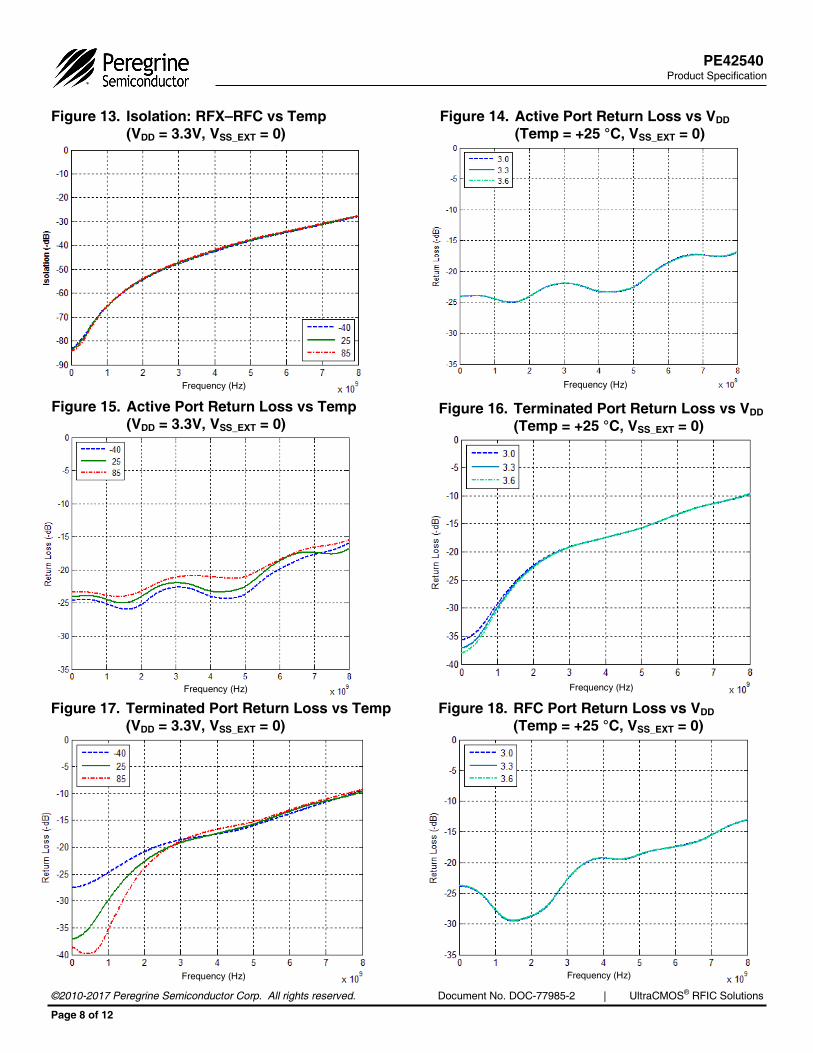
Figure 13. Isolation: RFX–RFC vs Temp
(VDD = 3.3V, VSS_EXT = 0)
Frequency (Hz)
Figure 14. Active Port Return Loss vs VDD
(Temp = +25 °C, VSS_EXT = 0)
Frequency (Hz)
Frequency (Hz)
Frequency (Hz) Frequency (Hz)
Frequency (Hz)
Figure 15. Active Port Return Loss vs Temp
(VDD = 3.3V, VSS_EXT = 0)
Figure 17. Terminated Port Return Loss vs Temp
(VDD = 3.3V, VSS_EXT = 0)
Figure 16. Terminated Port Return Loss vs VDD
(Temp = +25 °C, VSS_EXT = 0)
Figure 18. RFC Port Return Loss vs VDD
(Temp = +25 °C, VSS_EXT = 0)

©2010-2017 Peregrine Semiconductor Corp. All rights reserved. Document No. DOC-77985-2 | www.psemi.com
PE42540
Page 9 of 12
Product Specification
0
20
40
60
80
100
120
10.0E+3 100.0E+3 1.0E+6 10.0E+6 100.0E+6 1.0E+9 10.0E+9
Lin
ea
rity
[d
Bm
]
Frequency [Hz]
PE42540 Linearity Performance
Nominal IIP3[dBm]
Nominal IIP2[dBm]
Figure 20. Linearity Performance
(Temp = +25 °C, VDD = 3.3V, VSS_EXT = 0)
Frequency (Hz)
Lin
eari
ty (
dB
m)
Figure 19. RFC Port Return Loss vs Temp
(VDD = 3.3V, VSS_EXT = 0)
Frequency (Hz)
1.0E+10

Document No. DOC-77985-2 | UltraCMOS® RFIC Solutions
Page 10 of 12
©2010-2017 Peregrine Semiconductor Corp. All rights reserved.
PE42540 Product Specification
Figure 22. Evaluation Board Schematic
DOC-32927
Figure 21. Evaluation Board Layout
PRT-28605
Evaluation Kit
The SP4T switch evaluation board was designed to ease customer evaluation of Peregrine’s PE42540. The RF common port is connected through a 50Ω transmission line via the top SMA connector, J1. RF1, RF2, RF3 and RF4 are connected through 50Ω transmission lines via SMA connectors J2, J4, J3 and J5, respectively. A through 50Ω transmission is available via SMA connectors J6 and J7. This transmission line can be used to estimate the loss of the PCB over the environmental conditions being evaluated.
R1 1M0603
R5 00402
J8PZC36DABNHEADER14
11
33
55
77
22
44
66
88
1010
1212
1414
1313
99
1111
C60.1 µF0402
J2142-0761-881
1
2
R2 1M0603
J1142-0761-881
1
2
J7142-0761-881
1
2
C222 pF0402
J5142-0761-881
1
2
R6 00402
J6142-0761-881
1
2
U1PE42540
GN
D1
RF27
GN
D3
GN
D4
GN
D6
GN
D5
RF
C13
GN
D8
GN
D9
GN
D10
RF42
GN
D12
GN
D16
RF118
RF323
GN
D11
VD
D27
GN
D14
V1
29
V2
30
VS
S31
GN
D15
GN
D17
GN
D20
GN
D21
GN
D22
GN
D24
GN
D25
GN
D26
GN
D28
GN
D19
GN
D32
C122 pF0402
C50.1 µF0402
C422 pF0402
R4 00402
J4142-0761-881
1
2
C322 pF0402
R3 00402
J3142-0761-881
1
2
RF3
RF1
RF4
RF2

©2010-2017 Peregrine Semiconductor Corp. All rights reserved. Document No. DOC-77985-2 | www.psemi.com
PE42540
Page 11 of 12
Product Specification
TOP VIEW BOTTOM VIEW
SIDE VIEW
RECOMMENDED LAND PATTERN
A
0.10 C
(2X)
C
0.10 C
0.05 C
SEATING PLANE
B
0.10 C
(2X)
0.10 C A B
0.05 C
ALL FEATURES
5.00
5.00
Pin #1 Corner
3.03±0.05
3.03±0.05
3.50
0.435±0.050
(x32)
0.50
0.34
(x32)
0.26±0.05
(x32)
0.24
0.70
1.01 MAX
18
9
16
17 24
25
32
3.50
0.34
(x32)
3.08
3.08
4.90
4.90
0.50
(x28)
DETAIL A
DETAIL B
0.485
(x32)(x28)
0.11
0.10
0.10
0.535
0.04
0.15
DETAIL A DETAIL B
0.424
45° CHAMFER
Figure 23. Package Drawing
DOC-01877
Figure 24. Marking Specifications
42540
YYWW
ZZZZZZZ
YYWW = Date Code
ZZZZZZZ = Assembly lot code (maximum seven characters)
DOC-65743
Document No. DOC-77985-2 | UltraCMOS® RFIC Solutions
Page 12 of 12
©2010-2017 Peregrine Semiconductor Corp. All rights reserved.
PE42540 Product Specification
Device Orientation in Tape
Top ofDevice
Pin 1
Tape Feed Direction
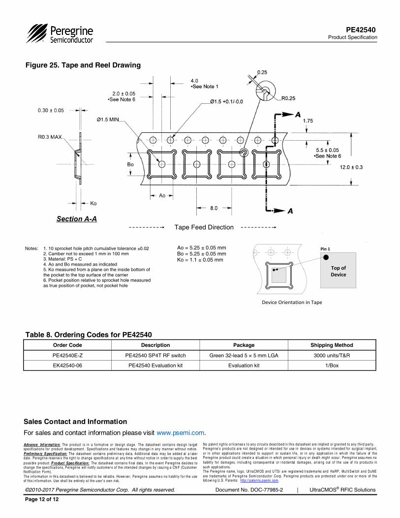
Notes: 1. 10 sprocket hole pitch cumulative tolerance ±0.02 2. Camber not to exceed 1 mm in 100 mm 3. Material: PS + C 4. Ao and Bo measured as indicated 5. Ko measured from a plane on the inside bottom of
the pocket to the top surface of the carrier 6. Pocket position relative to sprocket hole measured
as true position of pocket, not pocket hole
Ao = 5.25 ± 0.05 mm Bo = 5.25 ± 0.05 mm Ko = 1.1 ± 0.05 mm
Figure 25. Tape and Reel Drawing
Table 8. Ordering Codes for PE42540
Order Code Description Package Shipping Method
PE42540E-Z PE42540 SP4T RF switch Green 32-lead 5 × 5 mm LGA 3000 units/T&R
EK42540-06 PE42540 Evaluation kit Evaluation kit 1/Box
Advance Inf ormat ion: The product i s i n a formati ve or desi gn stage. The datasheet contai ns desi gn target specifi cati ons for product devel opment . Speci fi cati ons and features may change i n any manner without noti ce.
Prelimina ry S pecif ication: The datasheet contai ns preli mi nary data. Addi ti onal data may be added at a l ater date. Peregri ne reserve s the ri ght to change specifi cati ons at any ti me without noti ce i n order to suppl y the best
possi bl e product. P roduct Spec ificat ion: The datasheet contai ns fi nal data. In the event Peregri ne deci des to change the speci fi cati ons, Peregri ne will notif y customer s of the i ntended changes by i ssui ng a CN F (Customer Notifi cati on Form).
The i n formati on i n thi s datasheet i s beli eved to be reli abl e. Howe ver, Peregri ne assume s no li abili t y for the use of thi s i n formati on. Use shall be enti rel y at the user’ s own ri sk.
No patent ri ghts or li cense s to any ci rcui ts descri bed i n thi s datasheet are i mpli ed or granted to any thi rd party. Peregri ne’ s products are not desi gned or i ntended for use i n devi ces or sy stems i ntended for surgi ca l i mpl ant,
or i n other appli cati ons i ntended to support or sustai n li fe, or i n any appli cati on i n whi ch the fail ure of the Peregri ne product coul d create a si tuati on i n whi ch personal i nj ury or death mi ght occur. Peregri ne assu mes no
liabilit y for damages, i ncl udi ng consequenti al or i nci dental damages, ari si ng out of the use of i t s products i n
such appli cati ons. The Peregri ne name, l ogo, Ul t raCM OS and U TS i are regi stered t rademarks and HaRP, Mul ti Swi tch and DuNE
are t rademarks of Peregri ne Semi conductor Corp. Peregri ne products are protected under one or more of the foll owi ng U.S . Patents: h ttp:/ /patents.psemi.com.
Sales Contact and Information
For sales and contact information please visit www.psemi.com.