Embed Size (px)
Citation preview

The NorCal FCC-2 Assembly & Operating
Manual Rev. 1
3-21-06
Copyright 2006 W3CD - All rights reserved
1

Contents 1. Introduction............................................................................................................. 5
2. FCC-2 Specifications ........................................................................................... 7
3. Assembly Notes ..................................................................................................... 8
3.1 Essential Tools and Equipment................................................................................. 8
3.2 SMT Soldering Tips.................................................................................................. 8
3.3 Parts Bag Component Locator.................................................................................. 9
4. Assembly ............................................................................................................... 11
4.1 Side A Assembly .................................................................................................... 11
4.2 Side B Assembly..................................................................................................... 17
5. Initial Testing ....................................................................................................... 26
6. Calibration............................................................................................................. 28
6.1 DDS Calibration Using WWV ............................................................................... 28
6.2 DDS Calibration Using a Broadcast Station........................................................... 28
6.3 Frequency Counter Calibration............................................................................... 29
7. FCC-2 I/O.............................................................................................................. 30
7.1 FSK Input................................................................................................................ 30
7.2 KEY Output ............................................................................................................ 30
7.3 Lo-Z Output ............................................................................................................ 30
7.4 Hi-Z Output............................................................................................................. 32
8. VFO Operation..................................................................................................... 33
8.1 LCD Display ........................................................................................................... 33
8.2 Switch Operations................................................................................................... 34
8.3 Keying..................................................................................................................... 35
9. Programmable Frequency Memories ............................................................. 36
10. FCC-2 Frequency Calculations ..................................................................... 38
10.1 Algorithm 1 – Basic Receive DDS Output Frequency Calculation...................... 39
10.2 Algorithm 2 – Basic Transmit DDS Output Frequency Calculation .................... 40
10.3 Algorithm 3 – FSK Receive DDS Output Frequency Calculation ....................... 41
10.4 Algorithm 4 – FSK Transmit DDS Output Frequency Calculation...................... 42
11. FCC-2 VFO Programming ............................................................................. 43
11.1 FCC Mode............................................................................................................. 44
11.2 VFO Mode ............................................................................................................ 44
2

11.3 Shaft PB ................................................................................................................ 45
11.4 VFO Limit............................................................................................................. 45
11.5 RX IF .................................................................................................................... 45
11.6 TX IF..................................................................................................................... 46
11.7 Band ...................................................................................................................... 46
11.8 RX Calc................................................................................................................. 46
11.9 RX Scale ............................................................................................................... 47
11.10 TX Calc............................................................................................................... 47
11.11 TX Scale ............................................................................................................. 47
11.12 DDS Cal.............................................................................................................. 47
11.13 TX Space Off ...................................................................................................... 48
11.14 TX Mark Off ....................................................................................................... 48
11.15 RX Mark Off....................................................................................................... 48
12. Frequency Counter Programming................................................................. 48
12.1 Band ...................................................................................................................... 49
12.2 Gate....................................................................................................................... 49
12.3 IF Frequency ......................................................................................................... 49
12.4 Display .................................................................................................................. 49
12.5 Prescale ................................................................................................................. 50
12.6 User Band ............................................................................................................. 50
12.7 CTR Cal ................................................................................................................ 50
13. Circuit Description............................................................................................ 50
APPENDIX A. FCC-2 Component Layout – Side A..................................... 53
APPENDIX B. FCC-2 Component Layout – Side B ..................................... 54
APPENDIX C. FCC-2 Schematic ....................................................................... 55
APPENDIX D. FCC-2 Connections ................................................................... 56
APPENDIX E. FCC-2 Band Display.................................................................. 57
APPENDIX F. Parts List ...................................................................................... 58
APPENDIX G. Default FCC-2 Firmware Parameters ................................... 59
3
Figures and Tables
Figure 1. Bag 1 Contents ................................................................................................ 10 Figure 2. Bag 2 Contents ................................................................................................ 10 Figure 3. C2, R1, R2, U1, U4 Locations ........................................................................ 11 Figure 4. Q1 and Q2 Locations...................................................................................... 12 Figure 5. 0.1uF Capacitor Locations............................................................................. 13 Figure 6. 6.8K Resistor Locations ................................................................................. 13 Figure 7. R9, R10 and R16 Locations ........................................................................... 14 Figure 8. C14, C15 and C16 Locations ......................................................................... 15 Figure 9. D1, D2, R22, R23 Locations ........................................................................... 15 Figure 10. C6, 10K Resistor Locations.......................................................................... 16 Figure 11. U6 Location ................................................................................................... 17 Figure 12. U2, C3, C4 Locations.................................................................................... 18 Figure 13. U3 Positioning ............................................................................................... 19 Figure 14. R12, R19, R17, R21, R24 Locations ............................................................ 19 Figure 15. R7, R20 Locations......................................................................................... 20 Figure 16. C5, C7, C13, C17 Locations ......................................................................... 21 Figure 17. Locations for C18, C19, C20, C21, L1, L2, L3........................................... 21 Figure 18. U5 Installation............................................................................................... 23 Figure 19.Completed Side A .......................................................................................... 24 Figure 20. Completed Side B.......................................................................................... 24 Figure 21. FCC-1 JP5 Installation................................................................................. 25 Figure 22. Completed Assembly .................................................................................... 26 Figure 23. Operational FCC-2 Display ......................................................................... 27 Figure 24. LO-Z FCC-2 Output Response ................................................................... 31 Figure 25. Hi-Z Output Response.................................................................................. 32 Figure 26. VFO Display.................................................................................................. 33 Figure 27. Suggested T-R Switching Logic................................................................... 36 Figure 28. Typical Memory Mode Display ................................................................... 37 Figure 29. VFO Display in Memory Mode ................................................................... 37 Table 1. Programmable VFO Parameters.................................................................... 44 Table 2. Band-limited Frequency Ranges..................................................................... 45 Table 3. Programmable Frequency Counter Parameters........................................... 49 Table 4. J1 Connections.................................................................................................. 56 Table 5. J2 Connections.................................................................................................. 56 Table 6. J3 Connections.................................................................................................. 56 Table 7. J4 RS-232 Signal Connections......................................................................... 56 Table 8. J5 Signal Connections ...................................................................................... 56 Table 9. Band Select Inputs vs. LCD Band Display .................................................... 57 Table 10. General VFO Parameters.............................................................................. 59 Table 11. 160m - 17m and Dir Band VFO parameters ............................................... 59 Table 12. 15m to 10m Band VFO parameters.............................................................. 59 Table 13. 6m VFO Parameters ...................................................................................... 59 Table 14. 2m VFO Parameters ...................................................................................... 60
4

1. Introduction The NorCal FCC-2 is an add-on DDS VFO board that extends the basic capabilities of the FCC-1 counter kit. All of the FCC-1 features have been retained, so you won’t lose them by upgrading. A lot of work has been put into this kit to minimize power consumption and permit battery operation for extended periods. Surface mount technology (SMT) has been used extensively to minimize the size and weight of the kit. The FCC-2 is peerless in its low power consumption and flexibility. The kit features a DC - 20MHz DDS (Direct Digital Synthesis) chip, a shaft encoder and provides RTTY support. A new PIC microcontroller is supplied with the kit, which adds the VFO to the basic counter features. The VFO firmware supports 13 bands from 160m through 2m, plus a non-specific, Direct band. There are numerous user-programmable parameters which are stored in EEPROM for one-time setup convenience. You can easily switch between VFO and frequency counter modes and the DDS output will retain its frequency. You’ll see later on how we use this feature to calibrate the counter. The user-programmable IF offsets and scale factors permit the VFO to operate in a wide range of HF and VHF applications. The prescale feature permits down-stream frequency multiplication or for use as a reference source for a PLL synthesizer. The LCD displays the actual output frequency. Dual VFOs and Split operation are supported in the firmware, and the FCC-2 will operate RTTY straight off your workbench. Just connect a COM port cable and launch the software. I’ve used MMTTY and it works great. You can incorporate the FCC-1/2 combination into a homebrew rig or package them into a separate enclosure for use as a portable test instrument. Typical current consumption for the pair is less than 60mA. Operation is as simple as connecting a power supply. If you ordered the FCC-2 kit with the DDS chip, it will be included in one of the component bags. If you chose the lower cost option and haven’t yet ordered the AD9834BRU sample from Analog Devices, point your browser to http://www.analog.com . Search for AD9834 and scroll down the page to order a sample. New users will need to register first, but it’s quick and straightforward. Your new DDS chip will be in the mail shortly and best of all, it’s totally free! The kit contains all of the essential parts. All you need to supply are your favorite pin headers. Over 90% of the components are SMT. To successfully assemble the FCC-2, you need to have previous kit building experience, preferably with SMT components. It’s not recommended that beginners attempt this project because of its intricate nature. If you find yourself in over your head after purchasing the kit, no problem. You can have the SMT components installed by Kit Builders. Send Mike, WA6OUW, an email at [email protected] for further information. It’s a good idea to read through the manual before beginning to get a better understanding of the steps involved and the unit’s capabilities. You’ll find a lot of useful information and application ideas in the following pages before you warm up your soldering iron.
5

FCC-2 Features
• Complete FCC-1 Frequency Counter support • Shaft encoder for frequency entry, Memory and Menu mode operations • 4 pushbutton and shaft encoder user interface • Dual VFOs • Split operation • VFO copy: A-> B, B->A • VFO can be band limited or full range • Fast T-R switching • FSK (RTTY) support • 10 programmable frequency memories, store and recall to/from either VFO • Last band frequency used is stored in EEPROM – after 30 second dwell • Programmable transmit IF offset • Programmable receive IF offset • Programmable transmit frequency scaling: 1 to 255 - per band • Programmable receive frequency scaling: 1 to 255 - per band • Programmable transmit frequency calculation per band:
o Direct o VFO+IF o VFO-IF o IF-VFO
• Programmable receive frequency calculation per band: o Direct o VFO+IF o VFO-IF o IF-VFO
• Programmable transmit RTTY Mark frequency offset – 2125 Hz nominal • Programmable transmit RTTY Space shift frequency – 170 Hz nominal • Programmable receive RTTY Mark frequency offset • Programmable shaft encoder pushbutton function • DDS Calibrate mode • Extensive Menu mode • Computer-controlled contest keying
6

2. FCC-2 Specifications
Dimensions 1.5” x 3.0” x 1.25” (HWD)
Weight 1.2 oz.
Power Requirements 30 mA in addition to FCC-1. Inputs FCC-1 connection
RS-232 compatible FSK input: TXD, RTS, Ground Usable Frequency Range DC to >20 MHz Outputs: 1. Lo-Z:
50 Ohm, 20KHz – 18 MHz output (-3dB) 3.0mw (4.7dBm) to 25mw (14 dBm) @ 1MHz typ. Usable from 10KHz to 21 MHz.
2. Hi-Z: 600 Ohm, DC-18 MHz output,
580mVpp typical. 3.Key Out:
Active low, open collector, computer controlled via RTS
DDS Lowpass Filter 7th order Elliptic T-R turnaround delay 1mS max.
Frequency Memories 10, user programmable Band Memories 13, frequency is automatically stored after 30
second dwell Receive IF Offset 0 to >268 MHz.
Transmit IF Offset 0 to >268 MHz
Receive Prescale Factor 1 to 255, programmable per band
Transmit Prescale Factor 1 to 255, programmable per band
FSK Mark Frequency Offset 0 to >268MHz
FSK Space Frequency Offset 0 to >268MHz
Supported Bands 160m, 80m, 60m, 40m, 30m, 20m, 17m, 15m, 12m, 10m, 6m, 2m, Direct
Controls Shaft Encoder with built-in pushbutton
Encoder Pushbutton Programmable: Decade Increment, VFO A/B select
7

3. Assembly Notes Before beginning assembly of the FCC-2, you should have completed building, testing and calibration of the FCC-1. FCC-2 testing and calibration depend on a fully functioning FCC-1 board. The FCC-2 uses about 60 components, most of which are SMT (surface mount technology). It can be built in a few hours, depending on the builder’s experience. Patience is a big plus, since components are placed close together to optimize the signal integrity. You will need proper tools and equipment to build and calibrate this kit.
3.1 Essential Tools and Equipment
1. .010” (preferred) or 0.015” diameter rosin core solder 2. A temperature-controlled soldering iron. 600F – 700F 3. Soldering iron tip diameter of 1/32” or smaller 4. .1” wide or narrower solder wick 5. Round point tweezers 6. A cookie sheet with raised sides is helpful to avoid losing parts 7. Headband or illuminated magnifier 8. A 10x – 14x jeweler’s loupe is highly desirable for inspecting IC soldering 9. Adequate lighting 10. Masking tape to hold the board during assembly 11. Digital Mutlimeter (DMM) with milliamp range 12. Receiver capable of receiving 10MHz WWV -or- standard AM medium wave
broadcast band receiver. 13. 47 to 51 Ohm ¼ watt carbon or metal film resistor 14. Oscilloscope 15. A frequency counter is helpful, but not necessary
3.2 SMT Soldering Tips
Lead-based solder is being phased out, but 60/40 or 63/37 tin/lead rosin-core, .010” to .015” diameter solder is suitable for installing the surface-mount components in this kit. You can use .025” diameter solder for the thru-hole components. Silver-bearing, “eutectic” solder is also acceptable, but not necessary. Under no circumstances should you use solder with an acid-core flux. In my experience working with SMT, a 700oF tip temperature works very well. It allows a minimum contact time before the solder flows into the joint. A cooler tip temperature requires a longer contact time which can damage a component. I use a .02” conical tip with a 30o bend because it permits me to hold the iron at a comfortable angle. The small tip diameter is necessary for attaching the TSSOP devices, U5, the AD9834. You will have difficulty avoiding solder bridges if you use
8

a larger tip diameter. If you inadvertently create a bridge, use the solder wick to remove it, then reapply a small amount of solder to the joint. Fine point tweezers are useful for removing splinters, but aren’t the best for holding SMT components. I use Erem EROP2ASA round point tweezers to hold SMT components while soldering. These are available from Mouser, cat. no. 578-EROP2ASA, and the cost is mere $3.35 at the time of writing. Avoid hemostats: they will crush the parts or send them flying. You can build the FCC-2 on a small cookie sheet to catch any parts that may escape your grasp. The need for good lighting and magnification can’t be overemphasized. A pair of 100 Watt incandescent lamps on either side of the work surface is a good choice for most people. For magnification, I use an inexpensive headband magnifier because it provides 3D viewing and has a basic magnification of 2.2x. Extra flip down lenses increase it up to 4.8x. The highest power is necessary for inspecting IC soldering. A good quality jeweler’s loupe can be purchased for less than $15.00. A popular online auction lists these and the headband magnifiers. Luke Enriquez, VK3EM, wrote a great SMT tutorial. You can view it online at: http://www.geocities.com/vk3em/smtguide/websmt.html He suggests applying liquid flux from a pen or syringe. I’ve found that 1206 resistors and caps will solder just fine without the flux, but it’s good to use on ICs because it cleans the joint and solder readily flows into it. It’s not cheap, but a little goes a long way. You should clean the excess flux after soldering with isopropyl alcohol or acetone and a cotton swab.
Most, if not all, of the thru-hole kits you’ve assembled in the past have had a component side and a solder side to the PC board. The parts are mounted on one side and soldered on the other. This concept doesn’t apply to the FCC-2 because thru-hole and SMT parts are mounted on both sides of the board. Instead, the sides are identified as Side A and Side B. The side is silkscreened on the board above J1. The assembly instructions below are organized to permit ease of component installation. The silkscreen component outlines indicate the component locations and orientation. Appendices A and B contain enlarged views of Side A and Side B, respectively.
3.3 Parts Bag Component Locator The FCC-2 parts are packaged in 3 bags. Bags 1 and 2 contain the surface mount parts. Bag 3 contains through-hole and miscellaneous parts. Bags 1 & 2 have compartments to hold the SMT parts. To access a part, cut a slot in the compartment and remove it. When there is a strip of parts in the compartment, you will be instructed how to install them. Figures 1 & 2 below show the contents of Bags 1 & 2. Print them and use them as a reference because some of the parts are not marked. The figures show the reference designator, generic part number, and any value appearing on the part, in quotes.
9

C222uF Tant
"22u"
C1,5,7-13,17.1uF
C4, 6.01uF
C141pF
C19, 2033pF
C162.7pF
C18, 2115pF
C153.3pF
C310uF Tant
"10u"
D1, D21N4148W
"T4"
R130.9K"3092"
R2226K
"2263"
Q1, Q2MMBT3904
"1A"
L1-33.9 uH"3R9"
Figure 1. Bag 1 Contents
R3,5,6,116.8K"682"
R1049.9
"49R9"
R7, 19200
"200R"
R20402
"402R"
R9, 16225
"225R"
R21432
"432R"
R4,8,13-15,1810K
"103"
U1LM2931C"2931C"
R22, 2322K
"223"
U2LM3480-3.3
"LOA"
U4,6LT1395CS5
"TMA"
U3ASV50 MHz
Empty R171K
Figure 2. Bag 2 Contents
10

4. Assembly
The FCC-2 board is small, and I found it helpful to secure it to a surface using masking tape. Since components are oriented vertically and horizontally, feel free to reposition the board for comfortable soldering, especially with the ICs.
4.1 Side A Assembly
Orient the FCC-2 board with the silkscreened Side A facing up. Tape the board to your work surface or cookie sheet. We will be using the components in Bags1 and 2 for this side.
Remove U1, LM2931, from the bag 2. The IC has a broad band at the pin 1 end. Refer to Figure 3 for placement. Position it squarely over the U1 pads and tack down pin 1. Inspect the positioning to make sure all of the IC leads rest squarely over the remaining pads. Once you are satisfied with the placement, solder pin 5 to lock the position, then solder the remaining pins. Inspect your work carefully to make sure all of the joints resemble the photo.
U1 Pin 1
C2 Stripe226K
30.9K
U4 Pin 1
Figure 3. C2, R1, R2, U1, U4 Locations
Remove one of the LT1395CS5 chips from Bag 2. Save the other for Side B. This IC is marked LTMA. Position it over the pads of U4 as shown in Figure 3 and tack down pin 1. Make sure all of the pins are aligned with the pads and solder pin 4, diagonally opposite pin 1. Solder the remaining pins.
11
Remove the 30.9K resistor from Bag 1. It is marked 3092. Install it at R1.
Remove the 226K resistor from Bag 1.It is marked 2263. Install it at R2.
Remove C2, 22uF, from Bag 1. It is marked either 226C or 22u. Install is as shown in Figure 3 with the stripe facing the “+” sign silkscreened on the board.
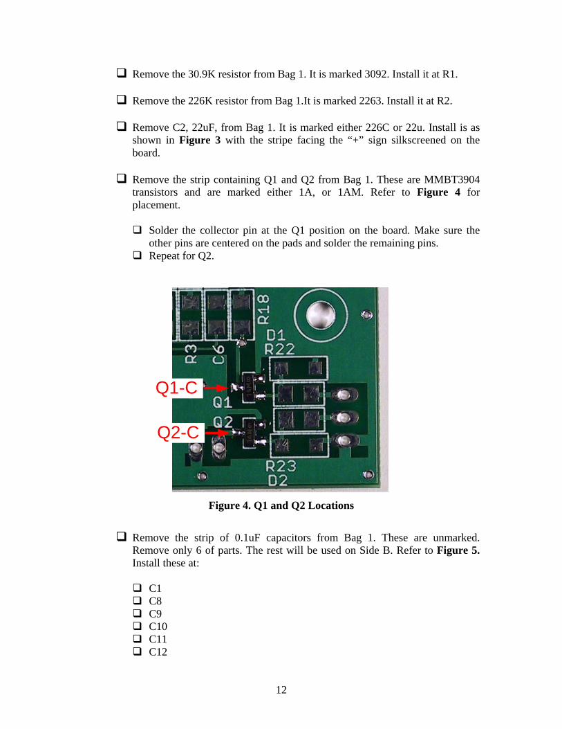
Remove the strip containing Q1 and Q2 from Bag 1. These are MMBT3904 transistors and are marked either 1A, or 1AM. Refer to Figure 4 for placement.
Solder the collector pin at the Q1 position on the board. Make sure the
other pins are centered on the pads and solder the remaining pins. Repeat for Q2.
Q1-C
Q2-C
Figure 4. Q1 and Q2 Locations
Remove the strip of 0.1uF capacitors from Bag 1. These are unmarked. Remove only 6 of parts. The rest will be used on Side B. Refer to Figure 5. Install these at:
C1 C8 C9 C10 C11 C12
12

0.1uF
0.1uF
0.1uF
0.1uF
Figure 5. 0.1uF Capacitor Locations
Remove the strip of 6.8K resistors from Bag 2. These are marked 682. Refer to Figure 6. Install these at:
R3 R5 R6 R11
6.8K
6.8K
Figure 6. 6.8K Resistor Locations
13

Remove the 49.9 Ohm resistor from Bag 2. It is marked 49R9. Refer to Figure 7. Install it at R10.
49.9 Ohms
255 Ohms
Figure 7. R9, R10 and R16 Locations
Remove the strip of 255 Ohm resistors from Bag 2. These are marked either 2550 or 255R Refer to Figure 7. Install these at:
R9 R16
Remove C16 from Bag 1. This is a 2.7 pF capacitor and is unmarked. Install it at C16, as shown in Figure 8. This installation will require a little more heat and solder because of the via to the bottom copper layer.
Remove C15. This is a 3.3pF capacitor and is unmarked. Install it at C15, as shown in Figure 8. Like C16, use a little extra solder and heat to ensure a good solder joint
Remove C14. This is a 1pF capacitor and is unmarked. Install it at C14, as shown in Figure 8. Use a little extra heat and solder to make a solid joint.
14

2.7pF 3.3pF 1pF Figure 8. C14, C15 and C16 Locations
Remove the strip of 22K resistors from Bag 2. These are marked 223. Refer to Figure 9. Install them at:
R22 R23
22K
D2 Striped End
D1 Striped End
Figure 9. D1, D2, R22, R23 Locations
15

Remove the strip of 1N4148 diodes from Bag 1. These are marked T4. Refer to Figure 9. The striped ends are closest to Q1 and Q2. Install them at:
D1 D2
Remove one of the 0.01uF capacitors from Bag 1, save the other for Side B. The part is unmarked. Install it at C6, as shown in Figure 10.
10K
.01uF
10K
Figure 10. C6, 10K Resistor Locations
Remove the strip of 10K resistors from Bag 2. These are marked 103. Refer to Figure 10. Install them at:
R4 R8 R13 R14 R15 R18
This completes installation of the Side A surface mount components. It’s a good time to take a break. Afterwards, inspect your work. Look for cold solder joints and bridges, especially around U1 and U4.
16

If you’re assembling the board on a cookie sheet, remove it and place the board on a non-conductive surface. It’s time for a quick test. Set your DMM to measure resistance and connect the negative lead to J1 pin 1 and the positive lead to J1 pin 9. The resistance should be at least 100K. If it’s significantly less, a short exists. Reinspect your soldering, especially around U1 and C1, and correct any problems before proceeding.
Connect the positive lead of your DMM to the striped side of C2 and the negative lead to the other side. You should measure at least 15K Ohms once the capacitor charges up. If it’s lower than this, check your soldering around C9, C10, R4, R8 and U4 and correct any problems.
4.2 Side B Assembly
When your work on Side A is satisfactory, turn the board over with the silkscreened Side B at the top. Secure it to the work surface or cookie sheet with masking tape.
Remove U6, LT1395CS5 from Bag 2. This IC is marked LTMA. Position it over the pads of U6 as shown in Figure 11 and tack down pin 1. Make sure all of the pins are aligned with the pads and solder pin 4, diagonally opposite pin 1. Solder the remaining pins.
U6 Pin 1
Figure 11. U6 Location
17

Remove U2, LM3480-3.3 from Bag 2. This IC is marked LOA. Install it at U2, as shown in Figure 12.
LOA0.01uF
10uFStriped End
Figure 12. U2, C3, C4 Locations
Remove C3, 10uF tantalum capacitor, from Bag 1. It is marked either 106 or 10u. Refer to Figure 12 for placement and install it at C3. Make sure the striped end is closest to the silkscreened “+” sign.
Remove C4, 0.01uF, from Bag 1. This part is unmarked. Refer to Figure 12 and install it at C4.
Remove U3, the 50 MHz oscillator, from Bag 2. This part has gold-plated concave recesses for pins and gold pads on the bottom. Refer to Figure 13 for positioning.
Apply a small amount of solder to the pin 1 pad. Grasp the oscillator in
your tweezers, heat the pad and slide U3 into position. The 3 remaining recesses should line up with the pads. Adjust as necessary.
Solder the diagonally opposite pin, making sure that solder wicks up into
the recess. Repeat for the other pins. Add solder to U3 pin 1 so that it wicks into the recess.
18

U3 Pin 1
Figure 13. U3 Positioning
Remove the strip of 255 Ohm resistors from Bag 2. These are marked either 2550 or 255R. Refer to Figure 14. Install them at:
R12 R24
Apply SolderHere
255 Ohms
200 Ohms
432 Ohms Figure 14. R12, R19, R17, R21, R24 Locations
Remove R21, 432 Ohm resistor, from Bag 2. It is marked either 4320 or 432R. Refer to Figure 14. Install it at R21.
19

Remove R17, 1K pot, from Bag 2. Refer to Figure 14. Apply some solder to the pad closet to the R17 silkscreened legend. Grasp the part in your tweezers, heat the pad and slide the pot onto it. Align it with the silkscreened outline. The remaining two pads should be lined up with the pot leads. Use solder sparingly and solder the remaining leads.
Remove the strip of 200 Ohm resistors from Bag 2. These are marked either 201 or 200R. Refer to Figure 14 for the location of R19 and Figure 15 for the location of R7. Install these resistors at:
R7 R19
200 Ohms 402 Ohms
Figure 15. R7, R20 Locations
Remove R20, 402 Ohm resistor, from Bag 2. It is marked 402R. Refer to Figure 15. Install it at R20.
Remove the remaining strip of 0.1uF capacitors from Bag 1. These are unmarked. Refer to Figure 16. Install them at:
C5 C7 C13 C17
20

0.1uF
0.1uF
Figure 16. C5, C7, C13, C17 Locations
Remove the strip of 15pF capacitors from Bag 1. These are unmarked. Refer to Figure 17. Install them at:
C18 C21
3.9uH
15pF 15pF33pF 33pF
Figure 17. Locations for C18, C19, C20, C21, L1, L2, L3
21

Remove the strip of 33pF capacitors from Bag 1. These are unmarked. Refer to Figure 17. Install them at:
C19 C20
Remove the strip of 3.9uH inductors from Bag 1, These are marked 3R9. The inductors are wound on a ceramic core and only have metallization on the bottom side. The plastic top cover is fragile when heated. Don’t press on the inductors with a sharp object! Instead, grasp it by its sides. When installing them, place the inductor over the solder-coated pad and heat the pad until the inductor sinks into the molten solder. When the joint cools, heat the other pad and melt solder onto the pad, not the part. Refer to Figure 17 for placement. Install the inductors at:
L1 L2 L3
Remove the tape from the board and turn it over. Measure the DC resistance across C14, C15 and C16. Each should be around 3.5 Ohms. If the resistance is significantly higher, such as 10 Ohms or more, the inductor on the side opposite the cap was not soldered properly. Reheat the appropriate joints and retest until all resistance measurements are low.
Turn the board over to Side B and secure it to your work surface.
Remove U5, AD9834BRU, from its protective cover, being careful not to bend the leads. If they are inadvertently bent, use a hobby knife or other fine-point tool to straighten them. This is the most challenging component to install, and it was saved for last to give you experience with the other ICs. Refer to Figure 18. If you have liquid flux, apply a coating to the U5 pads.
Apply a small amount of solder to the pin 1 pad. Position the chip over the
pads and touch the soldering iron to pin 1 of the AD9834 to melt the solder. When the joint cools, inspect the positioning of the IC over the pads. This is close work and magnification is absolutely necessary. Make sure all of the IC leads line up with the rest of the pads and there is no overlap. If there is a small offset, you can probably get away with gently nudging the chip to achieve alignment. If it’s large, reheat pin 1 and reposition the chip.
When you are satisfied with the chip’s position, solder pin 11, which is
diagonally opposite pin 1. Go back to pin 1 and add a little solder to secure the joint.
22

Solder pins 20 and 10.
Now go down the pin1 side of U5 and solder each pin in succession.
Starting at pin 11, solder the remaining pins of U5.
Inspect your work very carefully. If there is a solder bridge, clear it using
the solder wick. Apply a small amount of solder to each pin and reinspect. Allow the chip to cool before attempting to correct bridges. Make sure the pins are soldered to the pads. Looks can be deceiving. If in doubt, reheat the joint. The soldering should resemble Figure 18 when you are done. There is a continuous bead of solder from the pin down to the pad. Liquid flux was used here to permit the free flow of solder. Use alcohol or acetone to remove the excess flux after soldering.
PIN 20
PIN 10
PIN 11
PIN 1
Figure 18. U5 Installation
Remove the board from the work surface.
Open Bag 3, which contains the thru-hole parts.
Install the right angle 10-pin header at J1 on Side B. The short pins are inserted into the board. Carefully position it so that the pins are parallel to the board and facing out as shown in Figure 20. Apply a small amount of solder to pin 1 and check the alignment of the pins. Reheat and adjust as necessary to
23

make them parallel to the board. Solder pin 10 to secure the position, then solder the remaining pins. Remember to add a little extra solder to pin 1 for a solid connection.
Turn the board over and install the shaft encoder on Side A. Make sure the shaft is perpendicular to the board. Turn the board over to Side B and solder the shaft encoder pins and mounting tabs. Don’t apply too much heat to the tabs to avoid damaging the encoder.
On Side B, install your favorite .1” connectors at J2, 3, 4 and 5.
This completes the basic board assembly. Carefully inspect the solder joints of the resistors, capacitors, transistors and diodes. They should be smooth and shiny. Retouch as necessary. Now examine the IC solder joints. The lead pitch is small and there is plenty of opportunity for solder bridges, especially at U5. Make sure there are no solder bridges across the pins or pads. Side A of the board should closely resemble Figure 19. Side B should look like Figure 20.
Figure 19. Completed Side A
Figure 20. Completed Side B
24

Set the FCC-2 aside and put the FCC-1 in front of you.
Insert the right angle SIP socket into the JP5 location on the bottom side of the FCC-1 board. Refer to Figure 21. That is, the side opposite the LCD. Make sure the body of the connector is flush and parallel to the FCC-1 board and tack solder pin 10. Recheck the alignment and then solder pin 1. Solder the remaining pins. Clip off the excess pin length.
Connector Flushand Parallel to
FCC-1 Figure 21. FCC-1 JP5 Installation
Remove U1 from the FCC-1 board and insert it into a piece of conductive foam or wrap it in aluminum foil. Put it in a safe place in case you want to revert to the basic frequency counter later.
Remove the new FCC-2 U1 from its antistatic foam and install it in the FCC-1 board. Note that U1 pin 1 is close to U3.
Carefully align the FCC-2 J1 pins with the socket on the FCC-1 board. Gently plug it in. There will be a small gap exposing the pins of FCC-2 J1. This is normal. The two boards should be in the same plane.
Install the knob on the shaft encoder. Congratulations, you’re done! The completed assembly is shown in Figure 22.
25

Figure 22. Completed Assembly
5. Initial Testing Disconnect any band switching, keying and frequency inputs from the FCC-1 board. Connect a 1/4W 47 to 51 Ohm resistor across FCC-2 J2.
Turn R17 on the FCC-2 board fully counter-clockwise. Connect an oscilloscope probe to J2 pin 2; the pin adjacent to the dot is ground.
Apply a 12 volt DC supply to FCC-1 JP1. Pin 1 is negative. The display should indicate FCC-2 on the top line and Ver 1.0 on the bottom. This will be displayed for about a second. The top line should then display 1,000.000 KHz. The second line should read Dir a , as shown in Figure 23.
26
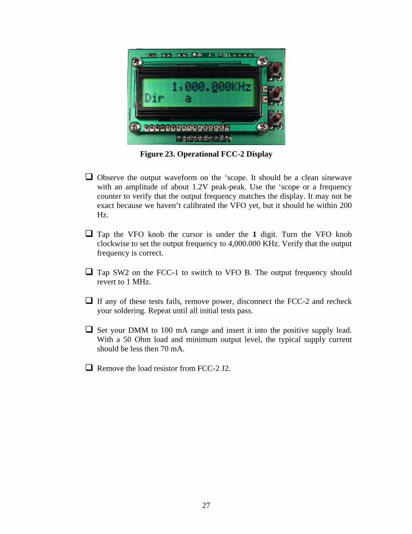
Figure 23. Operational FCC-2 Display
Observe the output waveform on the ‘scope. It should be a clean sinewave with an amplitude of about 1.2V peak-peak. Use the ‘scope or a frequency counter to verify that the output frequency matches the display. It may not be exact because we haven’t calibrated the VFO yet, but it should be within 200 Hz.
Tap the VFO knob the cursor is under the 1 digit. Turn the VFO knob clockwise to set the output frequency to 4,000.000 KHz. Verify that the output frequency is correct.
Tap SW2 on the FCC-1 to switch to VFO B. The output frequency should revert to 1 MHz.
If any of these tests fails, remove power, disconnect the FCC-2 and recheck your soldering. Repeat until all initial tests pass.
Set your DMM to 100 mA range and insert it into the positive supply lead. With a 50 Ohm load and minimum output level, the typical supply current should be less then 70 mA.
Remove the load resistor from FCC-2 J2.
27

6. Calibration
The DDS oscillator and frequency counter clock require separate calibrations. We will calibrate the DDS first. Before beginning calibration, apply 12V to the FCC-1 and let it warm up for at least 15 minutes. The most accurate way to calibrate the DDS oscillator is to zero beat the 10.000000 MHz calibration frequency with WWV. Users who are unable to receive the 10MHz WWV signal may use a local AM medium wave broadcast station as a reference. In most countries, broadcast station carriers must be within a few Hz of their allocated frequencies and you can use them as a secondary standard. Both calibration methods are described below. 6.1 DDS Calibration Using WWV Attach a short clip lead to FCC-2 J2 pin 2 and lightly couple it to a receiver tuned to 10 MHz. If your receiver has a whip antenna, you may need to separate it from the FCC-2 because of the strong calibration signal. If your receiver has a coax-fed antenna, the signal may be too weak. Try lifting the ground connection. Apply 12V to the FCC-1 and wait for it to begin operation. Press and hold SW3 for at least ½ second until the LCD displays Menu, then release. After about ½ second, the LCD should display FCC Mode on the top line and DDS VFO on the bottom. The VFO knob is used to select menu items. Rotate it counter-clockwise until DDS Cal is displayed on the top line. Gently tap the VFO knob to enter the DDS calibration function. The top line will display 10,000.000CAL and the bottom line will display 55E63B88, which is the hexadecimal equivalent of the DDS calibration constant. Tap SW1 twice to place the cursor under the B digit. Using the VFO knob, adjust the calibration constant up or down until the heterodyne frequency is as low as possible. Tap SW1 once to place the cursor under the least significant digit and fine tune using the VFO knob. You can easily achieve a beat frequency of less than 1Hz. Gently tap the VFO knob so the setting isn’t disturbed. This exits the DDS calibration mode. Tap SW3 to exit the Menu mode. The new calibration constant is stored in the PIC’s EEPROM, so you won’t need to repeat this at each power-up.
6.2 DDS Calibration Using a Broadcast Station
Tune a receiver to a strong local AM broadcast station at the upper end of the band. Attach a short clip lead to FCC-2 J2 pin 2 and place it near the receiver. Apply 12V to the FCC-1. Dial in the station’s frequency on the FCC-2 and observe the beat frequency. Adjust the clip lead position so that the FCC-2 signal doesn’t overload the receiver and blank out the broadcast station. The beat note should be clearly audible as a low frequency fluttering.
28

Follow the last two paragraphs of Section 6.1 with the following exception. After making an adjustment, press the shaft encoder. The FCC-2 output will return to the broadcast frequency. Observe if the beat note is higher or lower than the previous. Turn the shaft encoder in the opposite direction if the beat note is higher. Repeat these steps until the beat frequency is less than 1 Hz. The DDS output will be as accurate as the station’s frequency. Tap SW3 to exit the Menu mode. 6.3 Frequency Counter Calibration Recalibrating the frequency counter may be necessary because the PIC was changed and there are minor differences between devices. Since the DDS was just calibrated, we can use its output to check the counter calibration. Jumper FCC-2 J2 pin 2 to FCC-1 JP3 pin 2. Apply 12V to the FCC-1 and wait for it to begin operation. Set the VFO frequency to 10,000.000 KHz. Press and hold SW3 until the Menu message appears and then release. Turn the VFO knob until FCC Mode is displayed on the top line of the LCD. Tap the VFO knob and note that an asterisk (*) appears at the right side of the top line. Turn the VFO knob until Counter is displayed on the bottom line. Tap the knob; the asterisk will disappear. Turn the VFO knob until Gate appears on the top LCD line. Tap the knob to edit this entry. Turn the knob until 1 sec appears on the bottom line. Tap the VFO knob without disturbing this setting. Now tap SW3 to exit the menu mode and enter the frequency counter mode. The frequency display should agree with the VFO frequency to within a few Hz. If the difference exceeds 10 Hz, adjust C5 on the FCC-1. The FCC DDS and Frequency Counter are now calibrated and ready to use.
29

7. FCC-2 I/O
The FCC-2 has one input and three outputs: FSK IN, KEY OUT, Lo-Z and Hi-Z, respectively. Refer to Appendix E for the complete pinout listing for the connectors. The following sections describe the signals in detail. 7.1 FSK Input FSK IN is the optional connection to a computer COM port for FSK (RTTY) operation. The signals used are RTS, TXD and Ground. Table 7 in Appendix D shows how to connect the signals from a female DB-9 connector to the FCC-2. The RTS signal controls transmit/receive operation by driving the KEY OUT signal. The TXD signal is inverted and level shifted to drive the DDS FSEL pin. In FSK mode, this signal selects one of the DDS frequency registers to provide direct frequency shift keying of the DDS output. The FSK input can be left unconnected for normal VFO operating mode, or you can use the RTS signal to key the FCC-2 using a contest program. 7.2 KEY Output KEY OUT is used to control the FCC-2 transmit/receive mode by computer. Connect the FCC-2 Key Out, J5 pin 2, to the FCC-1 Key input, JP2 pin 2. No ground connection is necessary. You can also parallel any external key signal by connecting it to FCC-1 JP2. Make sure that the external key output is an open-circuit under key-up conditions.
The Key Output is open-collector and is controlled by an attached computer running a program such as MMTTY or a contest program. In receive mode, the RTS COM port signal is a negative voltage, and the Key output is essentially an open circuit. When transmitting the RTS signal goes positive, and the Key output is a low impedance to ground. 7.3 Lo-Z Output
The Lo-Z output is buffered by a 2-stage amplifier and has a 50 Ohm output impedance. It is an AC coupled and amplified output from the DDS and can drive any load resistance from an open circuit down to 50 Ohms. When terminated into 50 Ohms, the output power is adjustable from approx 3 mw to 25 mw at 1 MHz. R17 adjusts the output level. The non-loaded output voltage is adjustable from approx. 2.3Vpp to 6.5Vpp at 1MHz.
30

Figure 24 illustrates the typical Lo-Z output response with R17 adjusted to provide a +7 dBm output into a 50 Ohm load. The level varies with frequency for several reasons. The low frequency output is limited by coupling cap C11. This shouldn’t be an issue for most RF applications. There are a couple of factors that determine the high frequency roll-off. The primary one is the output response of the DDS chip. At 20 MHz, the DDS output level is –2.4 dB with respect to the 1 MHz output level. The output is attenuated as the frequency increases because of the inherent sin(x)/x response of the DDS DAC (digital to analog converter). This is due to sampling theory, not component limitations. You can plot this for yourself. Substitute 3.14159*Fout/50 MHz for x and plug it into your spreadsheet. Step Fout from .1 MHz to 50 MHz to observe the DDS output response. The DDS lowpass filter adds an extra 2dB of attenuation at 20MHz. This was a design compromise between flat response and alias frequency attenuation. When the DDS is producing a 20 MHz output, there is a strong spur at 30 MHz which needs to be attenuated. Use the Lo-Z output for your RF work. If the amplitude is too high, you can pad it down to the appropriate level. The buffer amp ensures that you have minimal attenuation at high frequencies.
+7dBm Frequency Response
-10.0
-9.0
-8.0
-7.0
-6.0
-5.0
-4.0
-3.0
-2.0
-1.0
0.0
1.0
0.01 0.1 1 10 100
Frequency - MHz
Rel
ativ
e O
utpu
t - d
B
Figure 24. LO-Z FCC-2 Output Response
31

7.4 Hi-Z Output
The Hi-Z output is an unbuffered, DC coupled output from the DDS low pass filter. It has a nominal 600 Ohm output impedance and is intended for use in audio applications. The open circuit AC output voltage is typically 600 mVpp at 1KHz. Since it is DC coupled, the AC signal rides on a DC bias of approx 300 mV. You must AC couple this signal externally with a capacitor and load with 10K Ohms or higher. Using a 100uF coupling cap, the output will be approx. –1 dB at 1Hz. Figure 25 shows the Hi-Z output response as measured with an oscilloscope. The 15pF probe capacitance loads the output at high frequencies, as the graph illustrates. Notice the 0.3dB output rise below 1KHz. This is caused by the high reactance of C17 at lower frequencies. The buffer amp bias network presents a 5K load, which is part of the elliptic filter termination. Below 1KHz, it’s essentially out of the circuit and the output level rises. For a constant level output in the audio passband, you can remove C17. Remember that this removes the signal from the Lo-Z output buffer. You will also need to change R21 to 402 Ohms to properly terminate the LPF.
Hi-Z Output Response
-9.0
-8.0
-7.0
-6.0
-5.0
-4.0
-3.0
-2.0
-1.0
0.0
1.0
1.E+00 1.E+01 1.E+02 1.E+03 1.E+04 1.E+05 1.E+06 1.E+07 1.E+08
Frequency - Hz
Rel
ativ
e O
utpu
t - d
B
Figure 25. Hi-Z Output Response
32

8. VFO Operation
The FCC-2 firmware supports two separate operating modes: Frequency Counter and VFO. The operation of the Frequency Counter is detailed in the FCC-1 manual, so it won’t be repeated in detail here. Refer to that manual for information on parameters and operation. The VFO operation is described below. Before we dive into all of the programmable features, let’s get familiar with the basic operation of the new firmware. We’ll cover the LCD display, switch and shaft encoder operation, and various operating modes. 8.1 LCD Display Refer to Figure 26. The VFO firmware displays information on both lines of the LCD. The frequency is displayed on the top line, with 1 Hz resolution. You can directly dial in frequencies in the range of 0 Hz to 452,984.831 KHz. Of course, the maximum DDS output is limited to 21 MHz. You can use the VHF frequency display for frequency multiplying or PLL applications. The firmware suppresses leading zeros on the display down to 1KHz. If you dial in, say, 500 Hz, the display will indicate 0.500KHz.
VFOFrequency
OperatingBand
ActiveVFO
SpecialMode Area
UnderlineCursor
Figure 26. VFO Display
The bottom line of the LCD displays operating conditions. At the left is the operating band, as selected by the FCC-1 Band Input. Thirteen bands are supported in the FCC-2 firmware: 160m – 2m, plus a direct band. Appendix E lists the displayed band vs. the FCC-1 band input. The currently selected VFO is displayed as single lower case letter in the center of the bottom line, a or b. The right side of the bottom line displays special conditions, such as Mem or split. We’ll cover this a little later.
33

When you first power up the FCC, the firmware places an underline cursor at the 100 Hz digit position. This is the lowest digit which will be modified as you turn the shaft encoder. You can change the digit position using one of the switches. 8.2 Switch Operations There are 4 switches that you can use to set the operation of the FCC-2. Switches SW1-3 are located on the FCC-1 and are used differently from the previous frequency counter software. The other switch is the shaft encoder pushbutton. For the purposes of this discussion, we’ll treat the shaft encoder as a switch, which it really is. SW1 has two functions. It used to position the frequency cursor and change split mode operation. You can tap SW1 on the FCC-1 to move the cursor left one digit position. If you hold it down, it will automatically advance after a brief pause. It will return to the 1 Hz digit position after advancing through the 100 MHz position. Pressing and holding SW1 together with SW2 toggles split operation. Hold the switches for about 1 second. The switches are placed close together so you can do this with one finger. When Split mode is active, the bottom right of the LCD will display split. Press and hold both switches again to exit the split mode.
SW2 has three functions in the non-split VFO mode. It is used for several other functions in Memory mode, which are covered later. Tapping SW2 selects the alternate VFO, a or b. The DDS output is immediately updated when this happens. If you hold it down for longer than ½ second, the active VFO, the one being displayed, is copied to the other, inactive one. The LCD will briefly display which VFO was copied. The third function is the split mode toggle, which was already described. When operating split, you can use SW2 to exchange transmit and receive VFOs. Let’s say you’re using VFO A for receive and VFO B for transmit. Tap SW2 to listen to the activity on your transmit frequency and make any frequency adjustments using the VFO knob. Tap it again to hear the rare DX or Fox station. SW3 has two functions. Tapping it enters the Memory mode, which is further described in Section 9. Tap the switch again to exit. If you press and hold SW3 for longer than ½ second, the Menu mode is entered. Section 11 covers Menu operations in detail. You tap SW3 again to exit the menu.
The shaft encoder has a built-in pushbutton. The FCC-2 firmware is shipped with this switch programmed to increment the frequency decade, and it works just like SW1, except there is no automatic repeat function. When adjusting the frequency, your hand never needs to leave the knob. You can change the shaft pushbutton operation to select alternate VFOs, which is described in the programming section. In this mode, it operates just like SW2, except that VFO copy is not supported. The encoder
34

pushbutton is also used in Memory and Menu modes to make certain things happen, and we’ll cover this later. Lastly, there’s the shaft encoder. You already know how it works to set the frequency. In the Memory mode, it is used to select a particular location. In Menu mode, you select a programmable parameter by turning the knob. The details are covered in their respective sections. In normal VFO operation, the firmware calculates a new pair of DDS values every time the encoder is turned: Receive DDS word and Transmit DDS word. The appropriate data is sent immediately to the DDS chip, depending on the state of the FCC-1 Key input. 8.3 Keying The firmware periodically samples the KEY input on FCC-1. You can drive this input with the FCC-2 KEY OUT signal, an external keyer, PTT switch, or any combination. The FCC-1 board pulls this input to +5V through a 10K resistor, which sets the default mode to Receive. When a logic 0 (Ground) level is detected, the firmware enters the transmit mode and the DDS transmit word is sent to the chip. When the KEY input ground is lifted, the firmware reverts to receive mode and sends the precalculated receive frequency data to the DDS chip. When operating split, the LCD will display the active VFO on the bottom line. Under key-up conditions, it will display your receive VFO, a or b, and the DDS output will reflect that VFO’s frequency, including any offsets and prescale values. When you key down, the display will switch to the other VFO, and the DDS output will change to the transmit VFO’s precalculated value. When you key up, the LCD display will persist for about ¼ second and show the transmit vfo and frequency to minimize display flicker. You can adjust the transmit VFO frequency under key down conditions. There is a small delay before the DDS updates its output after the KEY input changes. This delay varies depending on what the firmware happens to be doing, but the maximum delay is 1mS. You need to account for this in your application. An example block diagram is illustrated in Figure 27. In this example, the KEY signal controls transmit/receive switching directly, with no delay. In QRP rigs, it’s typically used to disable the receiver input. The transmit delay is started when the KEY input goes low and the DDS is still producing the receive frequency. When the delay expires, the DDS will be producing the correct output and the Transmit Enable output from the AND gate goes high, turning on the transmit stages. As soon as the KEY input goes high, Transmit Enable is deactivated, preventing transmission on the wrong frequency.
35
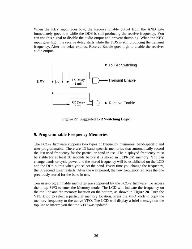
When the KEY input goes low, the Receive Enable output from the AND gate immediately goes low while the DDS is still producing the receive frequency. You can use this signal to disable the audio output and prevent thumping. When the KEY input goes high, the receive delay starts while the DDS is still producing the transmit frequency. After the delay expires, Receive Enable goes high to enable the receiver audio output.
TX Delay1 mS
To T/R Switching
Transmit Enable
RX Delay1mS
Receive Enable
KEY
Figure 27. Suggested T-R Switching Logic 9. Programmable Frequency Memories The FCC-2 firmware supports two types of frequency memories: band-specific and user-programmable. There are 13 band-specific memories that automatically record the last used frequency for the particular band in use. The displayed frequency must be stable for at least 30 seconds before it is stored in EEPROM memory. You can change bands or cycle power and the stored frequency will be established on the LCD and the DDS output when you select the band. Every time you change the frequency, the 30 second timer restarts. After the wait period, the new frequency replaces the one previously stored for the band in use.
Ten user-programmable memories are supported by the FCC-2 firmware. To access them, tap SW3 to enter the Memory mode. The LCD will indicate the frequency on the top line and the memory location on the bottom, as shown in Figure 28. Turn the VFO knob to select a particular memory location. Press the VFO knob to copy the memory frequency to the active VFO. The LCD will display a brief message on the top line to inform you that the VFO was updated.
36

MemoryLocation
StoredFrequency
Figure 28. Typical Memory Mode Display
SW2 on the FCC-1 board is used to preview a VFO frequency and store it in the programmable memory. It has tap and hold functions. Tapping SW2 does two things: it selects an alternate VFO and shows its current frequency setting. Tapping it twice returns to the current VFO. The display on the LCD will change and will resemble that shown in Figure 29. Here, the top line of the LCD displays the current VFO frequency. The bottom line displays the band, active VFO and the Mem annunciator to let you know you’re still in memory mode. The display will revert to the normal memory mode when you turn the VFO knob to select a different memory location. You can tap SW2 to review both VFO frequency settings without performing any memory store or recall operation.
ActiveMem Mode
Figure 29. VFO Display in Memory Mode
Once you have selected a particular target memory location and VFO frequency source, press and hold SW2 for longer than ½ second to store the new frequency in
37

the user-programmable memory. The LCD will briefly display a message indicating the memory location and which VFO’s frequency was stored. Once you’ve completed programmable memory store or recall operations, tap SW3 to return to normal VFO mode. 10. FCC-2 Frequency Calculations The frequency you dial in on the LCD is only part of the actual DDS output. A number of user-programmable parameters can modify the displayed frequency to produce useful DDS outputs in a variety of applications. I’ve tried to anticipate every situation, and this makes the frequency calculation a bit complicated. Rather than try to explain it in words, I’ll show the algorithms instead. For non-FSK operation, the FCC-2 produces an output frequency based on the separate calculations for transmit and receive. Algorithm 1 describes how the DDS output frequency is calculated for receive while Algorithm 2 describes DDS transmit calculations. Note that RX Calc, TX Calc, RX Scale and TX Scale are independent of each other, and you can program a unique value for each band. When operating in FSK mode, additional offsets are applied. Algorithms 3 and 4 describe how they are used.
The variables used in the algorithms are defined below:
Display Frequency: Value on the LCD RX Calc[BAND]: User-programmed offset calculation parameter, selected by band input RX Scale[BAND]: User-programmed DDS scale factor, selected by
band input RX Mark Off: User-programmable receive mark frequency offset TX Mark Off: User-programmed Mark transmit offset frequency FSK Off: User-programmed Space transmit offset from Mark VFO Frequency: Internal temporary variable DDS RX Output: Receive frequency produced by the DDS DDS TX Output: Transmit frequency produced by the DDS
BAND: FCC-1 band input value, 0 to 12
38

10.1 Algorithm 1 – Basic Receive DDS Output Frequency Calculation IF (RX Calc[BAND] = VFO + IF) VFO Frequency = Display Frequency + RX IF ELSE IF (RX Calc[BAND] = VFO – IF) VFO Frequency = Display Frequency – RX IF ELSE IF (RX Calc[BAND] = IF – VFO) VFO Frequency = RX IF – Display Frequency ELSE VFO Frequency = Display Frequency DDS RX Output = VFO Frequency / RX Scale[BAND] Suppose you’re going to use the FCC-2 as a local oscillator (LO) in a receiver that has an IF frequency of 4.912 MHz. You’re interested in receiving 160m, 1.8 MHz to 2.0 MHz. You can choose low side injection, and the DDS output will range from 3.112 MHz to 2.912 MHz. The LO and the RF will add up to the IF frequency, so the DDS RX Output frequency must decrease as the display frequency increases. To achieve this, program the 160m RX Calc value to IF-VFO. The RX Scale value is 1, since we don’t need to use any frequency multiplication to obtain the required frequency. Now, 3 MHz is pretty close to 2 MHz. It is better practice to use high side injection to move the local oscillator farther away from the receive frequency. In this case, the DDS RX Output frequency will range from 6.712 MHz to 6.912 MHz. Program the 160m RX Calc to VFO+ IF and RX Scale to 1 to obtain the proper DDS output.
At the opposite end of HF spectrum, suppose you want to listen to 10m, 28.0 to 29.7 MHz. The DDS isn’t capable of providing the proper frequencies with a 4.912 MHz IF, since it’s limited to 20 MHz. However, we can use a diode frequency doubler. Let’s use low side injection here, although high side would also work. The DDS output needs to be in the range of 11.544 to 12.394 MHz before frequency doubling to 23.088 to 24.788 MHz. Program the RX Calc to be VFO-IF and the RX Scale to 2 and the DDS will produce the required output frequencies.
For the VHF bands, higher orders of frequency multiplication must be employed. If you plan to use the FCC-2 with a “boatanchor” rig, it probably has this built in.
39

10.2 Algorithm 2 – Basic Transmit DDS Output Frequency Calculation IF (TX Calc[BAND] = VFO + IF)
VFO Frequency = Display Frequency + TX IF ELSE IF (TX Calc[BAND] = VFO – IF) VFO Frequency = Display Frequency – TX IF ELSE IF (TX Calc[BAND] = IF – VFO) VFO Frequency = TX IF – Display Frequency ELSE VFO Frequency = Display Frequency DDS TX Output = VFO Frequency / TX Scale[BAND]
On the transmit side, the DDS is capable of directly generating CW frequencies from 160m through 17m. If you’re incorporating the VFO into a rig that uses a premix oscillator, program the crystal frequency into the FCC-2 as the TX IF. The NorCal/Wilderness Sierra is one example of a rig that uses a transmit intermediate frequency. Note that the FCC-2 only supports one TX IF frequency. It’s better to bypass the premix stage and drive the transmitter directly for bands below 15m. To reach the higher bands, frequency multiplication must be employed. Consider using a simple diode frequency doubler to extend the DDS transmit range to beyond 10m. Set the TX Scale value to 2 for those bands where doubling is used. To reach 6m, the prescale value is preprogrammed to 3. The DDS output frequencies will range from 16.666667 MHz to 18.000000 MHz and external frequency tripling will need to be employed. For 2m, the default prescale value is 8, so the DDS output ranges from 18.000000 MHz to 18.500000 MHz. Of course, you can change these to suit your needs.
40

10.3 Algorithm 3 – FSK Receive DDS Output Frequency Calculation
IF (RX Calc[BAND] = VFO + IF) VFO Frequency = Display Frequency + RX IF ELSE IF (RX Calc[BAND] = VFO – IF) VFO Frequency = Display Frequency – RX IF ELSE IF (RX Calc[BAND] = IF – VFO) VFO Frequency = RX IF – Display Frequency ELSE VFO Frequency = Display Frequency DDS RX Output = (VFO Frequency - RX Mark Off) / RX Scale[BAND]
The difference between this algorithm and the one presented in Section 10.1 is the addition of the RX Mark Off value, highlighted in red. Current RTTY techniques typically use a computer and sound card to operate in FSK mode. The rig is set to operate in LSB and the display will indicate a certain frequency, say 7080.000 KHz, which is the frequency of the suppressed carrier. The actual received Mark frequency will be 2125 Hz lower, or 7077.875 KHz. The space frequency is 170 Hz lower than this, or 7077.705 KHz. In an LSB receiver tuned to 7080 KHz, the Mark frequency would be heard as a 2125 Hz tone and Space would be heard as 2295 Hz. This presents a problem for CW-only rigs since their bandwidth is much narrower. You can shift the DDS VFO receive frequency to put the Mark and Space tones within the bandpass of a CW rig by adjusting the RX Mark Off value. Let’s say your CW rig’s bandpass is centered on 700 Hz and has a width of 400 Hz. You’ll be able to hear tones from 500 Hz to 900 Hz. You can set the RX Mark Off value to 1.325KHz, which lowers the receive DDS output frequency. This will put the received Mark frequency at 800 Hz in the audio output. The Space tone will be received as 630 Hz. Both frequencies fall well within the passband. The RTTY software can be adjusted to use these new frequencies. To simplify the firmware, the RX Mark Off frequency has a very broad range. It is limited to the maximum IF Offset frequency, which is greater than 268 MHz.
41

10.4 Algorithm 4 – FSK Transmit DDS Output Frequency Calculation
IF (TX Calc[BAND] = VFO + IF) VFO Frequency = Display Frequency + TX IF ELSE IF (TX Calc[BAND] = VFO – IF) VFO Frequency = Display Frequency – TX IF ELSE IF (TX Calc[BAND] = IF – VFO) VFO Frequency = TX IF – Display Frequency ELSE VFO Frequency = Display Frequency DDS TX Mark Output = (VFO Frequency – TX Mark Off)
/ TX Scale[BAND] DDS TX Space Output = (VFO Frequency – TX Mark Off - FSK Off)
/ TX Scale[BAND]
Things get interesting when RTTY transmit mode is active. Besides the various offset and scaling operations described in Algorithm 2, Mark and Space frequency offsets are included. The DDS produces two output frequencies, which are controlled by the TX Mark Off and FSK Off parameters, highlighted in red. In FSK Mode, the default DDS output is the Mark frequency. This is produced when the RS-232 TXD input voltage is negative, or if it is left unconnected. The TX Mark Off value is subtracted from the VFO frequency on the display, regardless of any TX IF offset calculations. The FCC-2 firmware is shipped with this value preprogrammed as 2.125 KHz, so other stations can receive the correct Mark frequency in LSB mode. The FSK Off value is the Space frequency offset from Mark. The FCC-2 firmware is preprogrammed with a value of 0.170 KHz (170 Hz). This value, along with the TX Mark Off value is subtracted from the VFO frequency when the RS-232 TXD input is greater than +5V. Regardless of your receiver’s capabilities, the FCC-2 will produce the correct frequencies for reception by an LSB receiver. You can change the TX Mark Off and FSK Off parameters to other values for experimentation. Both the TX Mark Off and FSK Off limits are broad. The upper limit is greater than 268 MHz.
42

11. FCC-2 VFO Programming
The FCC-2 firmware uses a 2 level menu system: one for programmable VFO parameters and a second for frequency counter parameters. You had a brief experience with each when you performed the calibrations. When you modify the parameters, Key In on the FCC-1 is ignored. It’s a good practice to avoid editing the parameters while keying. We’ll explore the vfo parameters in detail in this section, beginning with an overview. The Frequency Counter programming is described in Section 12. The menu mode is entered and exited by using SW3. This button has dual functions. Tapping it enters the frequency memory mode when you’re using the VFO, covered in Section 10. Pressing and holding SW3 for ½ second enters the menu mode. Tapping it exits the menu mode and returns operation to normal mode. Go ahead and try this now. A review function is provided. After you enter the menu via SW3, you can scroll through the various parameters and view their settings by turning the VFO knob. This is true for all but the DDS and counter calibration modes. The DDS calibration constant is viewable only during active calibration. The frequency counter calibration has no associated constant, and once you enter this mode, you must cycle the power to exit. The FCC-2 firmware uses a “Tap – Turn – Tap” method for parameter editing. After selecting the parameter you want to modify, tap the VFO knob. This enters the edit mode and an asterisk, “*” will appear at the far right of the top line to remind you that you’re editing a parameter. Use the VFO knob to modify the parameter value. Tap it again to finish editing and store the new setting. The asterisk will disappear. There is no explicit save mode in the FCC-2 firmware. Any changes you make are automatically stored in EEPROM. There is a shortcut way to store a parameter. Once you’ve selected the desired value, you can tap SW3 to exit the Menu mode and save the changes. Operation in the selected mode will resume. The menu software maintains a pointer to the current menu entry. It is reset to select the FCC Mode parameter when power is first applied, but it remembers the last menu item you used when you exit the menu. If you return the item selection to FCC Mode, you can switch between DDS and Counter modes quickly. We’ll discuss the VFO parameter programming first, then review the frequency counter programming in Section 12. Appendix G lists the programmed parameters that are shipped with the kit.
43
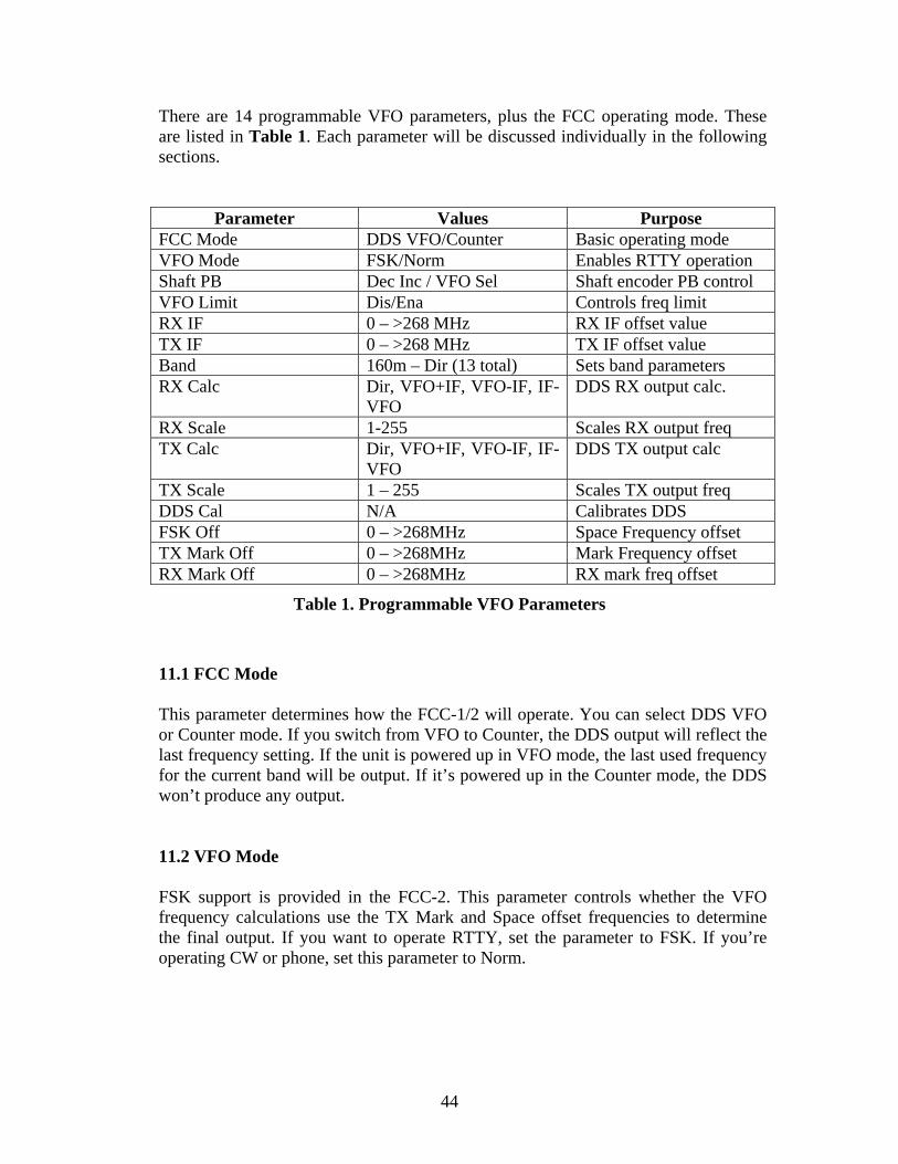
There are 14 programmable VFO parameters, plus the FCC operating mode. These are listed in Table 1. Each parameter will be discussed individually in the following sections.
Parameter Values Purpose FCC Mode DDS VFO/Counter Basic operating mode VFO Mode FSK/Norm Enables RTTY operation Shaft PB Dec Inc / VFO Sel Shaft encoder PB control VFO Limit Dis/Ena Controls freq limit RX IF 0 – >268 MHz RX IF offset value TX IF 0 – >268 MHz TX IF offset value Band 160m – Dir (13 total) Sets band parameters RX Calc Dir, VFO+IF, VFO-IF, IF-
VFO DDS RX output calc.
RX Scale 1-255 Scales RX output freq TX Calc Dir, VFO+IF, VFO-IF, IF-
VFO DDS TX output calc
TX Scale 1 – 255 Scales TX output freq DDS Cal N/A Calibrates DDS FSK Off 0 – >268MHz Space Frequency offset TX Mark Off 0 – >268MHz Mark Frequency offset RX Mark Off 0 – >268MHz RX mark freq offset
Table 1. Programmable VFO Parameters 11.1 FCC Mode This parameter determines how the FCC-1/2 will operate. You can select DDS VFO or Counter mode. If you switch from VFO to Counter, the DDS output will reflect the last frequency setting. If the unit is powered up in VFO mode, the last used frequency for the current band will be output. If it’s powered up in the Counter mode, the DDS won’t produce any output. 11.2 VFO Mode FSK support is provided in the FCC-2. This parameter controls whether the VFO frequency calculations use the TX Mark and Space offset frequencies to determine the final output. If you want to operate RTTY, set the parameter to FSK. If you’re operating CW or phone, set this parameter to Norm.
44

11.3 Shaft PB This parameter allows you to decide how the shaft pushbutton will be used in VFO mode. You can select Dec Inc to increment the frequency decade without moving your hand from the knob. Or, you can choose VFO Sel to permit you to toggle between VFO A and B. 11.4 VFO Limit The VFO can be used in many applications. You can impose a limit on the frequency coverage for any particular band or make it unlimited. You have the option to permit full frequency coverage, regardless of band. Table 2 lists the display frequency ranges for each band. The VFO frequency can be limited within a band, or it can span from DC-21 MHz in the same band.
VFO Band
Frequency Range (MHz)
160m 0 – 3.0 80m 2.5 – 5.0 60m 4.5 – 6.5 40m 6.0 – 8.0 30m 9.0 – 11.0 20m 13.0 – 15.5 17m 17.0 – 19.0 15m 20.0 – 22.0 12m 24.5 – 26.0 10m 26.0 – 32.0 6m 48.0 – 60.0 2m 135.0 – 160.0
Direct 0 - >452 MHz
Table 2. Band-limited Frequency Ranges
11.5 RX IF The RX IF parameter is used to modify the DDS frequency output to compensate for the receiver IF frequency, as described in Algorithm 1 in Section 10. The FCC-2 firmware only supports one RX IF offset. You can program IF offsets ranging from 0 Hz to 268,435.456 KHz. If you attempt to exceed this limit, the offset will peg at the maximum. Of course, the DDS is not capable of this frequency, but the RX Scale factor can modify it to put the DDS output within its range.
45

The FCC-2 firmware is shipped with the RX IF set to 0 Hz. Tap the VFO knob and dial in your receive IF frequency using the VFO knob. Use SW1 to select the appropriate decade you wish to modify. Tap the knob again to save the new offset frequency. 11.6 TX IF The TX IF parameter is used to modify the DDS frequency output to compensate for transmitter IF frequency, as described in Algorithm 2 in Section 10. Like the RX IF, the FCC-2 firmware only supports one TX IF offset. You can program IF offsets ranging from 0 Hz to 268,435.456 KHz. For ham bands from 160m through 20m, you can use the direct DDS output to drive the transmit stages directly, avoiding an intermediate mixing. The FCC-2 firmware is shipped with the TX IF set to 0 Hz. Tap the VFO knob and dial in your transmit IF frequency using the VFO knob. Use SW1 to select the appropriate decade you wish to modify. Tap the knob again to save the new offset frequency. 11.7 Band Each of the 13 bands supported by the FCC-2 firmware can have a unique way of calculating the DDS output frequency. To access the parameters for a particular band, use this menu item to select the desired band. The default selection is the hardware band input to the FCC-1. You can temporarily change this to access the band-specific values for the RX Calc, RX Scale, TX Calc and TX Scale parameters. 11.8 RX Calc The RX IF Offset calculation for the selected band is set using this menu item. The choices are: Dir VFO+IF VFO-IF IF-VFO The FCC-2 firmware is shipped with the calculation set to Dir for all bands. Check Algorithm 1 in Section 10 and decide how you want the receive DDS output frequency to be calculated.
46

11.9 RX Scale The value programmed in this parameter is used to divide the DDS receive output frequency by an integer. You can program this value from 1 to 255. The FCC-2 firmware is shipped with RX Scale set to 1 for the 160m through 17m bands. It is set to 2 for 15m, 12m and 10m. For 6m, the scale factor is 3 and for 2m it is 8. For the lower HF bands, you can probably leave this parameter set at the default value of 1. If you’re using some sort of frequency multiplication, you can adjust the scale factor up to 255. 11.10 TX Calc The TX IF Offset calculation for the selected band is set using this menu item. The choices are: Dir VFO+IF VFO-IF IF-VFO The FCC-2 firmware is shipped with the calculation set to Dir for all bands. Check Algorithm 2 in Section 10 and decide how you want the receive DDS output frequency to be calculated. 11.11 TX Scale
The FCC-2 is capable of directly generating the proper transmit frequency from 160m through 17m. The FCC-2 firmware is shipped with the TX Scale set to 1 for these bands. For 15m, 12m and 10m, frequency doubling is required and the TX Scale for these bands is preprogrammed at 2. For the VHF bands, higher multiplication factors are required. The TX Scale factor is preprogrammed to 3 for 6m and 8 for 2m.
11.12 DDS Cal The oscillator shipped with the FCC-2 has a nominal 50.000 MHz frequency. Manufacturing tolerances and operating temperature will change this. The result is that the DDS output frequency will differ from the displayed frequency by a small amount. You can adjust for oscillator variations using this menu selection. Follow the procedures outlined in Section 6.1 or 6.2 to calibrate the DDS output.
47
11.13 TX Space Off This value is used to modify the transmit Space frequency offset in FSK mode. Unless you wish to modify the Space offset for experimental purposes, you can accept this default offset of 170 Hz.
11.14 TX Mark Off When operating in FSK mode, this parameter sets the Mark frequency offset from the displayed value. The FCC-2 firmware is shipped with the conventional RTTY default of 2125 Hz. Remember that the offset is subtracted from the display setting for proper reception on an LSB receiver. 11.15 RX Mark Off The FCC-2 firmware is shipped with the default RX Mark frequency offset set to 0 Hz, to match the transmit offset. This is useful when your receiver has an SSB bandwidth. For receivers with a CW bandwidth, you will need to set this offset to a lower frequency. Try 1325 Hz as a starting point. You will still transmit at the proper offset for the other station to copy on an LSB receiver, but you will hear it’s transmissions at lower audio frequencies. 12. Frequency Counter Programming The FCC-2 firmware supports Frequency Counter operation just like the FCC-1 firmware, with a few differences. The most notable is that the shaft encoder is used to enter the values, instead of the pushbuttons. In this version of the firmware, the user band name length had to be reduced because of EEPROM size limits. Lastly, the counter calibration was moved to the menu. Use the Tap-Turn-Tap method to edit the counter parameters. Table XX lists the available parameters when you’re operating in the Counter mode. The FCC Mode was covered already in Section 11.1, so only the unique parameters will be described here. Refer to the FCC-1 manual for a detailed description.
48

Parameter Values Purpose
FCC Mode DDS VFO/Counter Basic operating mode Band 160m – 70cm, User & Dir Set band parameters Gate 100mS / 1 sec. Counting interval IF Frequency 0 – 268.435455 MHz IF Compensation Display Dir, VFO+IF, VFO-IF, IF-
VFO Display offset calculation
Prescale 0 – 255 Multiplies count value User Band Any 5-characters Custom band name CTR Cal None Counter Calibration
Table 3. Programmable Frequency Counter Parameters
12.1 Band The parameter is used to access the stored counter parameters. To access the parameters for a particular band, use this menu item to select the desired band. The default selection is the hardware band input to the FCC-1. Tap the VFO knob to change the band value and turn the knob. Tap it again when you’ve selected the desired band. When editing the other parameters, the band will appear in the upper right corner of the LCD for all but the last two parameters. 12.2 Gate
Set the counting interval using this parameter. For high accuracy measurements, select the 1 second period. The faster period has a resolution of 10Hz, which is probably accurate for most applications. This faster gate time will also improve responsiveness of the pushbuttons. 12.3 IF Frequency This parameter is used to modify the frequency count to compensate for receiver IF frequency, or transmit premix oscillator frequency. You can program IF offsets ranging from 0 Hz to 268,435.455 KHz.
12.4 Display This parameter instructs the firmware how to calculate the final display value given the input frequency, prescale and IF Frequency values. Section 9.5 of the FCC-1 manual provides a detailed description of the methods.
49

12.5 Prescale The prescale parameter is used to compensate for an upstream prescaler which divides a VHF or UHF frequency down to the range usable by the FCC. For applications where a prescaler is not used, set this value to 1. See Section 9.6 of the FCC-1 manual for further information.
12.6 User Band Like the FCC-1 firmware, you can program a unique name for the user band. Because high demand for EEPROM, the length of the user band name had to be reduced to 5 characters in the FCC-2 firmware. To edit the band name, tap the VFO knob to begin editing. The underline cursor will appear under the first character. Turn the knob to adjust the character. Tap SW1 to move the cursor right 1 position. Hold it down to repeatedly move it. When you’ve set the band name, tap the knob to finish editing. 12.7 CTR Cal
This menu item is used for frequency counter calibration. Tap the VFO knob to enter the calibration loop. The only way to exit is to cycle power. 13. Circuit Description The FCC-2 uses the Analog Devices AD9834 DDS chip, U5, to generate the output frequencies. This is a very low power device, which draws only 8mA. U3 is a low power 50 MHz clock oscillator which drives the DDS. Both devices are powered by 3.3V, which is regulated down from 5V by U2. The FCC-2 draws about 17mA from the +5V provided by the FCC-1. The DDS chip is programmed via a three-wire serial interface from the PIC on the FCC-1. Since the controller produces +5V signal levels, the SCLK, SDATA and FSYNC signals must be attenuated before presenting them to the DDS. R5, 6, 7 and R13, 14, 15 reduce the amplitudes to a level compatible with U5. The DDS produces complementary current outputs. The FCC-2 doesn’t use the IOUT signal, so it is terminated to ground through R7. The IOUTB signal is used to drive the output. The design calls for a 200 Ohm termination, which is formed by R20 and the 400 Ohm input impedance of the lowpass filter.
50

The lowpass filter is a 7th order elliptic designed for 400 Ohm input and output impedance and steep attenuation beyond 20 MHz. A deep null was placed at 50 MHz to effectively remove any clock signal from the output. The filter attenuation increases rapidly above 25 MHz to remove the DDS alias products. The filter output is terminated by R21 and the buffer amp biasing network. R19 is in series with LPF output to provide a nominal 600 Ohm output impedance at audio frequencies, available at J3. The buffer amp uses two LT1395 current-feedback opamps. These devices have a flat response beyond 100 MHz. U6 serves as a variable gain preamp with gains ranging from 2 to 6. R17 adjusts the output level. U7 is the output amp and has a gain of 2. The buffer is powered by a +10V supply which is produced by U1. Each opamp draws less than 5mA, no load. The total supply current increases when U4 is terminated into 50 Ohms. U1 is an adjustable low-dropout regulator. R1 and R2 set the output voltage to 10V. The maximum differential between input and output voltage is 200mV, which means that the minimum regulator input voltage must be 10.2V. Adding the 0.7V drop across D1 on the FCC-1, the minimum supply voltage should be at least 10.9V for proper operation. You can reduce this to 10.4V by changing FCC-1 D1 to a 1N5817 Schottky diode. The regulator degrades gracefully below the minimum threshold. When the input voltage drops below 10.9V, the regulator saturates and tracks the input voltage. However, it begins to draw current, up to an extra 12mA. The output buffer will still provide a stable output at reduced supply voltage, though the peaks may be clipped if a high gain is selected. At minimum gain, the buffers will provide an undistorted 1.8 mw output into 50 Ohms with a 7V supply voltage to the FCC-1. SW1 on the FCC-2 is a mechanical shaft encoder with 80 transitions per revolution. This was found to be too fast for comfortable operation, so the FCC-2 firmware divides it by 4 to 20. The encoder and pushbutton switch contact signals are sent directly to the FCC-1 board. An addition to the basic FCC-2 design was support for RTTY operation. RS-232 level TXD and RTS signals can be applied directly to J4, where they are level-shifted by R22, R23, D1, D2, Q1 and Q2. The TXDATA signal is normally negative, which cuts off Q1. Even if no COM port signal is connected, Q1 remains cutoff. This sends a logic 1 signal to the FSEL input on U5, selecting the Frequency 1 register. When the TXD signal goes positive, Q1 saturates and pulls the FSEL input low, selecting the DDS Frequency 0 DDS register. When the VFO mode is set to Norm, this signal is ignored.
51

The RTS signal is normally a negative voltage, or 0 volts if unconnected. In either case, Q2 remains cutoff. When the RST signal goes positive, Q2 saturates and pulls the KEY OUT signal to ground. This signal can be connected directly to FCC-1 JP2 pin 2 for computer-controlled transmit/receive keying. You’ll probably want to use an external keyer or PTT switch. Parallel any external keying across JP2, but make sure this input is also an open-circuit during key-up conditions. The 10K pullup resistor on the FCC-1 ensures a non-keyed state.
52

APPENDIX A. FCC-2 Component Layout – Side A
53
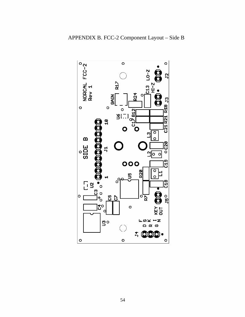
APPENDIX B. FCC-2 Component Layout – Side B
54
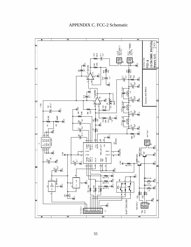
APPENDIX C. FCC-2 Schematic
55

APPENDIX D. FCC-2 Connections
J1 Pin Signal
1 GND 2 Encoder A 3 DDS Data 4 DDS Clock 5 DDS Fsync 6 Encoder PB 7 Encoder B 8 N.C. 9 +12V 10 +5V
Table 4. J1 Connections
J2 Pin Signal 1 GND 2 Lo-Z Output
Table 5. J2 Connections
J3 Pin Signal 1 GND 2 Hi-Z Output
Table 6. J3 Connections
J4 Pin Signal DB9 Pin
1 GND 5 2 RTS 7 3 TXDATA 3
Table 7. J4 RS-232 Signal Connections
J5 Pin Signal 1 GND 2 Key Out
Table 8. J5 Signal Connections
56
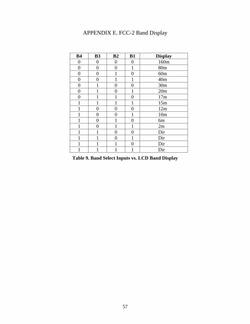
APPENDIX E. FCC-2 Band Display
B4 B3 B2 B1 Display 0 0 0 0 160m 0 0 0 1 80m 0 0 1 0 60m 0 0 1 1 40m 0 1 0 0 30m 0 1 0 1 20m 0 1 1 0 17m 1 1 1 1 15m 1 0 0 0 12m 1 0 0 1 10m 1 0 1 0 6m 1 0 1 1 2m 1 1 0 0 Dir 1 1 0 1 Dir 1 1 1 0 Dir 1 1 1 1 Dir
Table 9. Band Select Inputs vs. LCD Band Display
57
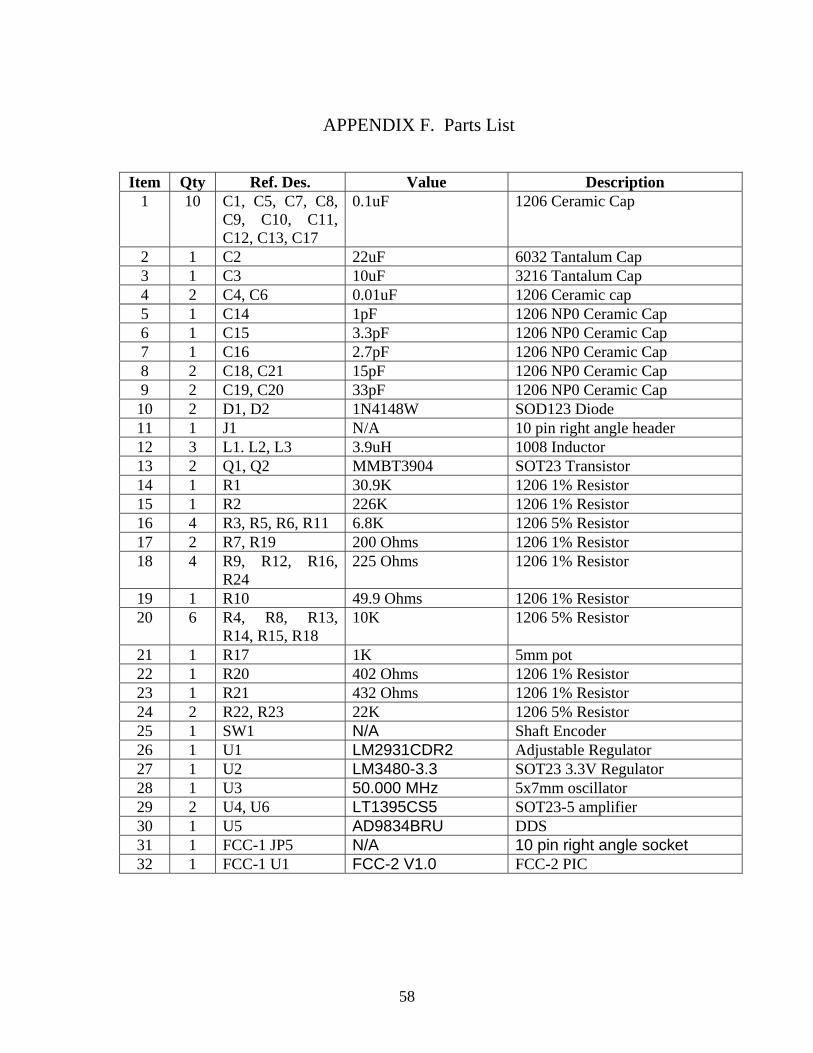
APPENDIX F. Parts List
Item Qty Ref. Des. Value Description 1 10 C1, C5, C7, C8,
C9, C10, C11, C12, C13, C17
0.1uF 1206 Ceramic Cap
2 1 C2 22uF 6032 Tantalum Cap 3 1 C3 10uF 3216 Tantalum Cap 4 2 C4, C6 0.01uF 1206 Ceramic cap 5 1 C14 1pF 1206 NP0 Ceramic Cap 6 1 C15 3.3pF 1206 NP0 Ceramic Cap 7 1 C16 2.7pF 1206 NP0 Ceramic Cap 8 2 C18, C21 15pF 1206 NP0 Ceramic Cap 9 2 C19, C20 33pF 1206 NP0 Ceramic Cap 10 2 D1, D2 1N4148W SOD123 Diode 11 1 J1 N/A 10 pin right angle header 12 3 L1. L2, L3 3.9uH 1008 Inductor 13 2 Q1, Q2 MMBT3904 SOT23 Transistor 14 1 R1 30.9K 1206 1% Resistor 15 1 R2 226K 1206 1% Resistor 16 4 R3, R5, R6, R11 6.8K 1206 5% Resistor 17 2 R7, R19 200 Ohms 1206 1% Resistor 18 4 R9, R12, R16,
R24 225 Ohms 1206 1% Resistor
19 1 R10 49.9 Ohms 1206 1% Resistor 20 6 R4, R8, R13,
R14, R15, R18 10K 1206 5% Resistor
21 1 R17 1K 5mm pot 22 1 R20 402 Ohms 1206 1% Resistor 23 1 R21 432 Ohms 1206 1% Resistor 24 2 R22, R23 22K 1206 5% Resistor 25 1 SW1 N/A Shaft Encoder 26 1 U1 LM2931CDR2 Adjustable Regulator 27 1 U2 LM3480-3.3 SOT23 3.3V Regulator 28 1 U3 50.000 MHz 5x7mm oscillator 29 2 U4, U6 LT1395CS5 SOT23-5 amplifier 30 1 U5 AD9834BRU DDS 31 1 FCC-1 JP5 N/A 10 pin right angle socket 32 1 FCC-1 U1 FCC-2 V1.0 FCC-2 PIC
58

APPENDIX G. Default FCC-2 Firmware Parameters
Parameter Shipped Value FCC Mode DDS VFO VFO Mode Norm Shaft PB Dec Inc VFO Limit Dis RX IF 0 KHz TX IF 0 KHz DDS Calibration value 55363B88 FSK Off 0.170 KHz TX Mark Off 2.125 KHz RX Mark Off 0 KHz
Table 10. General VFO Parameters
Parameter Shipped Value RX Calc Dir RX Scale 1 TX Calc Dir TX Scale 1
Table 11. 160m - 17m and Dir Band VFO parameters
Parameter Shipped Value RX Calc Dir RX Scale 2 TX Calc Dir TX Scale 2
Table 12. 15m to 10m Band VFO parameters
Parameter Shipped Value RX Calc Dir RX Scale 3 TX Calc Dir TX Scale 3
Table 13. 6m VFO Parameters
59

Parameter Shipped Value
RX Calc Dir RX Scale 8 TX Calc Dir TX Scale 8
Table 14. 2m VFO Parameters Frequency Counter Parameters
All of the Band Memories are shipped with the following values:
1. Gate: 100ms 2. IF Freq: 0.000KHz 3. Display: Direct 4. Prescale: 1 5. User Band “User ”
60