Embed Size (px)
Citation preview
Themicro-RWELLtechnology:statusandperspec:ves
G. Bencivennia, G. Felicia, R. Farinellib, M. Gattaa, L. Lavezzic, �
G. Morelloa, R. de Oliveirad, M. Poli Lenera, A. Ochie��
a. LNF-INFN�
b. INFN-Fe�
c. IHEP Beijing �
d. CERN�
e. Kobe University�
�
�
56thInterna:onalWinterMee:ngonNuclearPhysics,BormioJanuary23rd,2018

• They are composed of two elements: a cathode glued on a frame, working "as spacer and as limit for the conversion gas volume, and the μ-RWELL_PCB�
The μ-RWELL detectors
2
• The μ-RWELL_PCB is the core of the detector: this talk reports about its different versions developed taking into account the requirements of applications/experiments�
�
Why the resistive? Because of the micrometric distance between electrodes, every MPGD suffers from spark occurrence that can damage the detector or the FEE. �A resistive readout quenches the discharge: �
"- The Raether limit is overcome�"- The charge is deposited on the resistive layer �"- The charge density spreads with τ = RC "�"(M.Dixit, NIM A 518 (2004) 721) �"- The resistive layer is locally charged-up with a potential V=Ri, reducing
the ΔV applied to the amplification stage�"- The amplification field is reduced �"- The discharge is locally suppressed �
Obviously this has a drawback correlated to high particle fluence, that’s why we studied the performance of the detector as a function of the resistivity���
3

The single resistive layer • The simplest version of the detector, actually the first
one, has been extensively studied with several prototypes each characterized by different surface resistivities [JINST 10 P02008, NIM A 824 (2016) 565] �
• In this case the etched kapton foil, sputtered with DLC, is coupled through an insulating layer to the readout plane� topcopperlayer
kapton
resis/vefoil
pads
HV
Notinscale
5 μm Cu �50 μm Kapton�500 – 700 nm DLC �50 μm pre-preg �
4

Status of the single resistive layer
The R&D on the single resistive layer has been completed with the realization of two large area detectors of about 1.2 x 0.5 m2 in the framework of the CMS-phase2 muon upgrade �
5
These detectors have been realized in collaboration with Italian companies (ELTOS & MDT) within the TT project �Missing: space resolution with non-orthogonal tracks and R&D on the high rate scheme�
Several measurements have been already reported [PoS(Bormio2017)002]: gas gain, space resolution for orthogonal particle, time resolution and gain drop. �
6
β
z
x
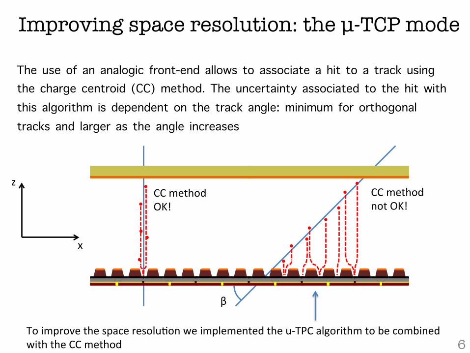
The use of an analogic front-end allows to associate a hit to a track using the charge centroid (CC) method. The uncertainty associated to the hit with this algorithm is dependent on the track angle: minimum for orthogonal tracks and larger as the angle increases �
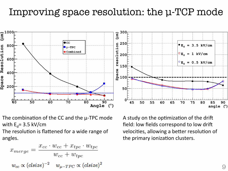
Improving space resolution: the μ-TCP mode
Toimprovethespaceresolu:onweimplementedtheu-TPCalgorithmtobecombinedwiththeCCmethod
CCmethodOK!
CCmethodnotOK!
Improving space resolution: the μ-TCP mode
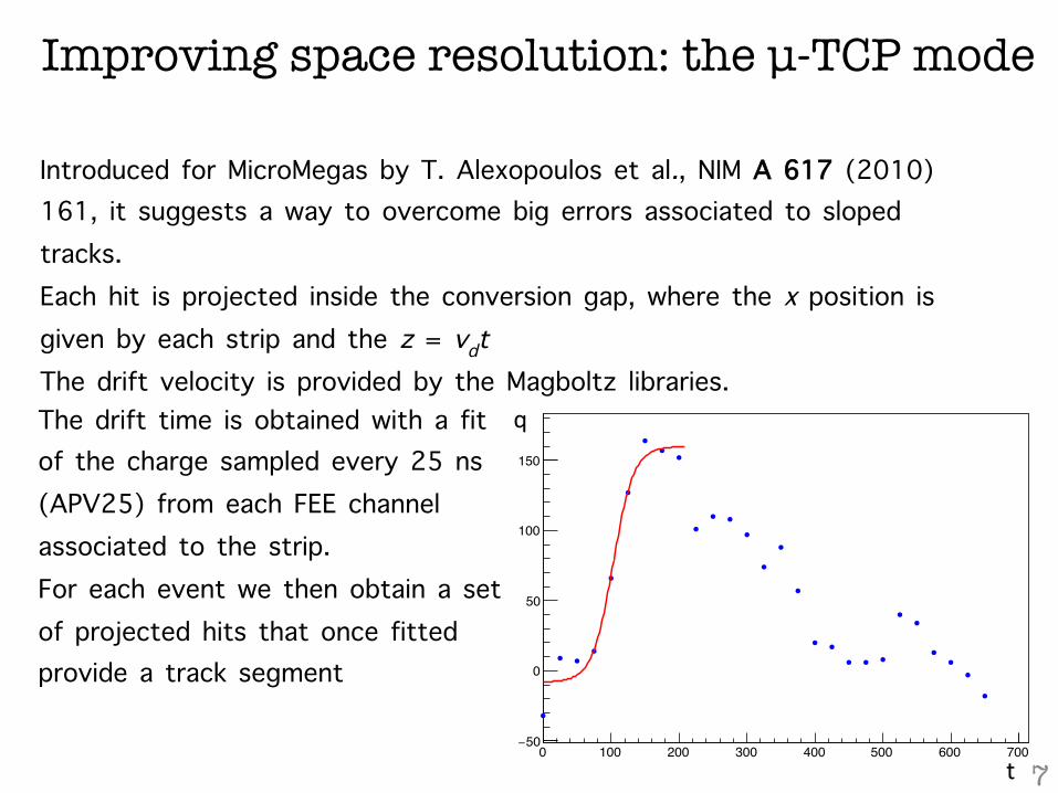
Introduced for MicroMegas by T. Alexopoulos et al., NIM A 617 (2010) 161, it suggests a way to overcome big errors associated to sloped tracks.�Each hit is projected inside the conversion gap, where the x position is given by each strip and the z = vdt�The drift velocity is provided by the Magboltz libraries. �
0 100 200 300 400 500 600 70050−
0
50
100
150
Graph
7
The drift time is obtained with a fit of the charge sampled every 25 ns (APV25) from each FEE channel associated to the strip. �For each event we then obtain a set of projected hits that once fitted provide a track segment�
q
t

Example of μ-TPC reconstruction
75° tracks� 45° tracks�
8
Here we have some examples where the tracks have an angle w.r.t. the readout plane of: �
arctan(3) = 71.5°�
arctan(2.8) = 70.3°�
arctan(0.83) = 39.8°�
arctan(0.97) = 44.1°�
z
z z
z
x
x
x
x
9
Improving space resolution: the μ-TCP mode
Thecombina:onoftheCCandtheμ-TPCmodewithEd=3.5kV/cmTheresolu:onisfla\enedforawiderangeofangles.
Astudyontheop:miza:onofthedri^field:lowfieldscorrespondtolowdri^veloci:es,allowingabe\erresolu:onoftheprimaryioniza:onclusters.

High rate version: the double resistive layer
10
• The charges collected on the resistive layer move towards the ground with a characteristic time τ(R,C) [Dixit et al, NIMA 518 (2004) 721, NIMA 566 (2006) 281]. �
• The idea is to reduce the path covered by the electrons on the DLC �
A matrix of conductive vias connects the two resistive layers. Another matrix of vias chains the second resistive
layer to ground through the readout�
5 μm Cu �50 μm Kapton�500 – 700 nm DLC �10 μm epoxy�500 – 700 nm DLC �50 μm epoxy� � �

The double resistive layer:
11 Detectors operated at a gain of 104. Beam spot ~2 cm2 (RMS2) �
Rate capability as a function of the pion beam intensity!
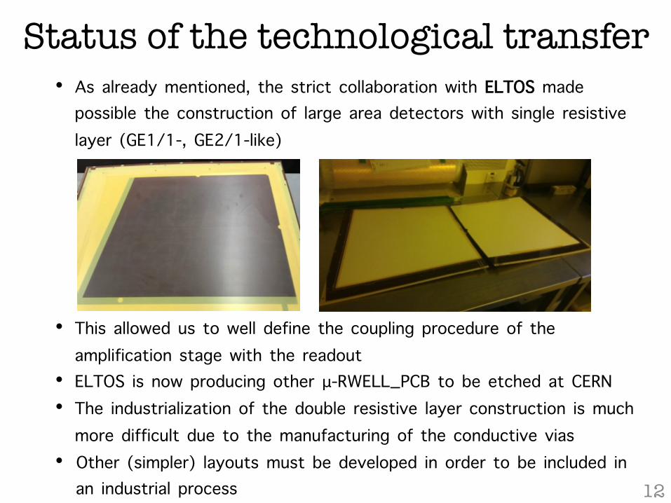
Status of the technological transfer
12
• As already mentioned, the strict collaboration with ELTOS made possible the construction of large area detectors with single resistive layer (GE1/1-, GE2/1-like) �
• This allowed us to well define the coupling procedure of the amplification stage with the readout�
• ELTOS is now producing other μ-RWELL_PCB to be etched at CERN �• The industrialization of the double resistive layer construction is much
more difficult due to the manufacturing of the conductive vias�• Other (simpler) layouts must be developed in order to be included in
an industrial process �

New layouts, new ideas, new challenges
13
The aim is to maintain a very short path for charges drifting on the resistive layer, while simplifying the construction process. �Two ideas are now under development: silver grid and resistive grid �
Silver Grid (SG) �Small conductive strips are screen-printed on the bottom part of the DLC �
Clearly the introduction of a conductive strip on the bottom layer of the amplification stage can induce strong instabilities due to discharges over the DLC surface. �
First prototypes of SG designed with safe geometrical parameters: grid pitch 6 mm, dead area around 1/3 of the total area�
dead area over the grid �
gridpitch
5 μm Cu �50 μm Kapton�500 – 700 nm DLC �pre-preg 50 μm � length=2178.73μm
length=244.96μm
DOCA

Silver Grid v1:�X-rays and H4 test beam (July 2017) • A SG μ-RWELL has been installed inside the RD51 tracking system and
characterized together with a Double Layer chamber �
At the H4 test beam we could supply up to 700 V, much more than for the other μ-RWELL without instabilities. The reason of a so high instability voltage is under investigation. �The lower efficiency is due to the geometrical effects. The increasing gain improves the collection efficiency partially compensating this leak. �A dedicated study on the minimum distance between the strip and the holes has been done to increase the efficiency� 14
Ar:CO2:CF4 45:15:40 �
96%
72%
geometricalefficiency

Silver Grid: optimization In order to reduce the dead area, we measured the Distance Of Closest Approach (without discharges) between two tips connected to a PS. We recorded the minimum distance as a function of the ΔV supplied for different foils before a discharge on the DLC occurs�
15
Two more prototypes delivered in November, with grid pitch 12 mm, dead area 1/10 of the active area �

Silver Grid: 2nd generation
16
The grid lines are connected to the ground through the resistance provided by the DLC itself (9-10 MΩ) �
The two detectors have been equipped with 6 x 8 mm2 pad-segmented readout �
557.76 μm � 34.13 μm � 1260.39 μm �

17
Silver Grid: 2nd generation
Ar:CO2:CF4 45:15:40 �
~12 mm�
The detector is mounted on a support moved by a stepper motor. The position is given within few tenths of millimeter. �Scan along the coordinate orthogonal to the grid lines direction �

Small resistive strips are screen-printed on the bottom side of DLC �
Resistive grid
The grid grounding is similar to the one used for the 2nd generation SG, as well as the readout segmented in pads. �Two prototypes designed with 6 mm grid pitch �
18 Grounding through DLC �

Resistive grid
19
Y distance of pads: �217.23 μm �
Resistive strip width: �296.99 μm �
X distance of pads: �105.03 μm �
No dead areas�
Grounding resistance: between 12 and 16 M�

Gain drop measurement with 5.9 keV X-ray
20
The gain drop is only due to Ohmic effect on the resistive layer: the charges collected on the DLC drift towards the ground facing an effective resistance Ω, depending on the evacuation scheme and computed by the parameter p0 �

Gain drop and efficiency
The primary ionization of 5.9 keV is ~7 times larger than the one created by a m.i.p. �In order to face a 3 MHz/cm2 m.i.p. fluence, with a 5% gain drop, the effective resistance Ω must be at maximum 2 MΩ. �Anyway a 5% drop of G0=6300 allows still to operate the detector at full efficiency. �A measurement of the efficiency with a high rate particles has been planned for the next test beam �
21
G0=6300 �G=0.95G0 �
NOEFFICIENCYLOSS

Conclusions & outlook • The single layer layout has been exploited to build large area detectors (~1/2
m2), but we also demonstrated that even larger detectors can be realized with the splicing technique, with the cooperation with ELTOS SpA, within TT �
• Several prototypes have been realized, with different simplified evacuation charge scheme for high rate purposes�
• Further optimization of the new high rate schemes must be done, addressed by the measurement of the gain drop done with X-rays�
�So far the best measured performances are: �• 1 MHz/cm2 rate capability with pion beam (Double Layer working at G=10000) �• space resolution 52 ± 6 μm (80 MΩ/☐, orthogonal tracks, no B field) �• well below 100 μm with non-orthogonal tracks, with the μ-TPC/CC combination �• time resolution 5.7 ns (with FEE saturation) �• Both the Silver Grid v1 reached a gain of almost 105 (to be understood) �• An ageing test at GIF++ is ongoing: the detector integrated up to 90 mC/cm2
without showing gain loss �
Spare

r
upperlayer
conduc:vevias inferiorlayer
singlelayerd d’
d(50cm)
(1cm)d’
Ω~ρsxd/2πr Ω’~ρs’x3d’/2πrΩ/Ω’~(ρs/ρs’)xd/3d’
Ifρs=ρs’àΩ/Ω’~ ρs/ρ’s*d/3d’=50/3=16.7
(*)point-likeirradia1on,r<<dΩistheresistanceseenbythecurrentgeneratedbyaradia1onincidentinthecenterofthedetectorcell
appendixA-B(G.Bencivennietal.,2015_JINST_10_P02008)
r
doublelayer
Thetwodifferentschemes

• The devices have been then tested at H4-SPS North Area, equipped with strips-segmented readout (400 μm pitch) and APV25 (CC method, orthogonl tracks) �
The single resistive layer: H4 test beam (2015)
σRWELL = (52±6) µm�@ B= 0T after TRKs contribution subtraction �
Ar:iC4H10 90:10 �
The different behaviour can be assigned to a different geometry of the amplification holes,
that have not been inspected. At lower resistivity the charge spread more, inducing a weaker signal on the pad. So the gain must
be increased to improve the efficiency �

The single resistive layer: GIF++ exposure (2017)
The study of ageing effects on DLC has been done by integrating the charge expected in 10 years of operation in the CMS GE2/1 region (1 kHz/cm2). �At a gain of 4000 the total charge expected is 2.6 mC/cm2 �
Ar:CO2 70:30 �
Ar:CO2:CF4 45:15:40 �
Ar:CO2 70:30 �
m.i.p.equivalentrate~10kHz/cm2

The double resistive layer: H8C test beam (2016)
5.7 ns�
Samesatura:onobservedinGEMdetectorsoperatedwiththesameFEEinthesametestbeam,whilewithGEMa:meresolu:onof4.8nshasbeenobtained
byLHCb[G.Bencivennietal.,NIMA494(2002)156]
Two double resistive layer prototypes have been tested with muon beam and equipped with VFAT2 �
Ar:CO2:CF4 45:15:40 �
ThankstoL.Benussi,L.Borgonovi,P.Giacomelli,A.Ranieri,M.Ressegor,I.Vai