Embed Size (px)
Citation preview
THE MECHANISM OF FORMATION OF STRUCTURAL V-DEFECTS
IN POLAR AND SEMIPOLAR EPITAXIAL GaN FILMS
SYNTHESIZED ON SiC/Si(111) AND SiC/Si(100)
HETEROSTRUCTURES
V.N. Bessolov1,3
, E.V. Konenkova1,3
, A.V. Zubkova2, A.V. Osipov
3,4, T.A. Orlova
1,
S.N. Rodin1, S.A. Kukushkin
3,4,5*
1A.F. Ioffe Physical-Technical Institute, Polytechnicheskaya 26, St. Petersburg, 194021, Russia
2St. Petersburg State V.I. Ul’yanov (Lenin) Electrical Engineering University, St. Petersburg, Russia
3Institute of Problems of Mechanical Engineering, Bolshoi pr. 61, V.O., St. Petersburg, 199178, Russia
4St.-Petersburg Academic University, Khlopina 8/3, St.-Petersburg, 194021, Russia
5St. Petersburg State Polytechnical University, Polytechnicheskaya 29, St. Petersburg, 195251, Russia
*e-mail: [email protected]
Abstract. The past results related to the main features of formation of structural V-defects in
polar GaN(0001) and semi-polar epitaxial GaN films are presented. The GaN films have been
synthesized by hydride-chloride vapor-phase epitaxy (HVPE) on two different substrates
Si(111) and Si(100) with an intermediate nano-SiC epitaxial layer. The nano-SiC layer has
been formed by a method of atom substitution on the Si substrate. The experimental studies
have demonstrated that V-defects on the surface of GaN(0001) films are regular hexagons of
30 μm in size, while on the surface of GaN V-defects are of the order of 1 μm. It was found
that V-defects on the semipolar face are extended along the 3211 direction. The size of
oblique facets of V-defects on the surface of polar GaN(0001) is of about 1 μm, while on the
surface of semipolar GaN )0111( layer they are much less, measuring about 150 nm, on the
average. On the basis of thermodynamics, the mechanisms of nucleation of V-defects on polar
and semipolar faces of GaN epitaxial films are elucidated, and the criteria of the formation of
V-defects are theoretically derived. A good qualitative agreement between the experimental
results and the theoretical model was found.
1. Introduction.
Present-day needs for substrates with semi-polar GaN layers for the production of light
diodes [1] and lasers [2] grow steadily. This is due to the fact that the use of polar structures
in quantum-dimensional (QW) III-nitride opto-electronic devices is associated with the Stark-
effect [3] which is brought about by strong piezoelectric polarization in polar structures. In
the case of semi-polar structures, the piezoelectric polarization is absent, and this opens up
new prospects in the production of devices of a new generation on the basis of semi-polar (Al,
Ga, In)N structures.
Substrates for growing of semipolar structures are usually synthesized by the following
way. Initially the thick epitaxial layers of polar GaN (0001) should be grown. Then the grown
up epitaxial GaN layers are cut in such a way that semipolar planes would crop out on the
Materials Physics and Mechanics 21 (2014) 266-274 Received: October 29, 2014
© 2014, Institute of Problems of Mechanical Engineering
crystal surface. After that, these semipolar planes are polished. The surface area of substrates
so produced is not large and depends on a thickness of an initial GaN (0001) layer. The
thicker the layer of an initial polar GaN film, the larger is the area occupied by GaN semi-
polar plane. Thick crack-free layers of GaN, as is well known, are difficult to grow. That is
why the fabrication of semipolar substrates with the use of thick GaN layers is a labor
consuming and highly expensive process.
The search for synthesis of GaN semipolar epitaxial films on previously prepared
foreign substrates is now actively pursued. For this purpose the n-, r-Al2O3 sapphire substrates
are coming into use [4]. However, that to use them as substrates for growing of GaN
semipolar layers, both substrates of Al2O3 and of thick GaN must be preliminary prepared. At
present, the producers of light-emitting diodes are making efforts to grow the substrates up to
12 inches in diameter [3]. Sapphire and silicon carbide substrates of such a size are not
currently produced as yet. Moreover, if this were the case, the price would be unproperly
high. In this regard, only sapphire substrates are most promising for the synthesis of structures
on the basis of gallium nitride.
The authors of papers [5, 6], whose results are generalized in the review [3], proposed
for a first time to use for the production of GaN semipolar films silicon (Si) plates coated
previously with a nano-layer of epitaxial silicon carbide (SiC). It is appropriate to note that for
the synthesis of GaN semipolar films, a nano-layer of SiC was grown up by a new atom
substitution method, advanced in papers [7, 8]. The mechanism of growth of SiC, in this case,
is fundamentally different from the classic method of growth of SiC on Si. As a result, the
epitaxial films of semipolar GaN have been obtained on Si(210) [5] and Si(001) [6].
One should mention, that for the synthesis of both semipolar and polar GaN layers, the
commonly accepted methods are used; these are epitaxy from organometallic compounds
(MOCVD) [9], hydride-chloride vapor-phase epitaxy (HVPE) [3-6] and molecular beam
epitaxy (MBE) [10].
The main factor retarding an intensive introducing of heterostructures based on GaN
into the production is the high content of various type defects. On the surface of gallium
nitride heterostructures there are originated so called V-defects [11-13], which are etching
pits, usually with a crystalline faceting, located on the surface of the GaN film. The structure
of V-defects formed on the GaN(0001) surface is well studied [11-13]. Thus, several models
have been proposed [13, 14], in which the V-defects were suggested to be formed due to the
interaction of dislocations [13] or due to elastic stresses in heterolayers [15]. According to the
advanced hypothesis, elastic stresses lead to the lower velocity of the growth on the )0111(
plane compared with that on the plane (0001).
When studying the growth mechanism of GaN semipolar layers on Si and on Si coated
with a layer of SiC [3, 5, 6], we have revealed that on the surface of GaN semipolar layers the
V-defects are formed. As far as we know, up to now, the studies of morphology and
nucleation mechanism of V-defects on the surface of GaN/Si semipolar layers have not been
carried out. In this connection, our goal was to elucidate experimentally this problem for GaN
semipolar layers grown up on carbide substrates of (111) and (001) orientations, coated with a
nano-layer of epitaxial SiC.
2. Experiment
The nitride layers were synthesized by a combined method. At the first stage, the SiC layer
was formed on Si(111) and Si(001) by using the atom substitution method [7, 8]. The
thickness of SiC layer on Si(111) was of about 90 nm, and that on Si(001) of about 30 nm.
After that, with the aid of HVPE method, the buffer AlN layer of thickness ranged from 300
to 1000 nm was formed. Then the basic layer of GaN has been deposited. That to synthesize
the GaN film on the surface of Si(111), the technology described in [16] has been applied. In
267The mechanism of formation of structural V-defects in polar and semipolar epitaxial GaN films...
the process of the further experiment the GaN(0001) layer with a thickness of about 100 μm
was grown up. On the surface Si(001) disoriented in the direction [110] by 2-7 °, the layer has
been growing by the method described in [5]. The thickness of the GaN )0111( layer was
15 μm. The structural characteristics of so produced films of GaN(0001)/AlN/SiC/Si(111) and
GaN )0111( /AlN/SiC/Si(001) and their morphology have been studied by different methods:
these are atomic-force microscopy (AFM), scanning electron microscopy (SEM), x-ray
diffractometry and x-ray luminescence.
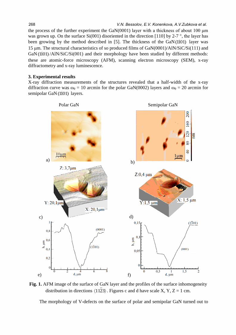
3. Experimental results
X-ray diffraction measurements of the structures revealed that a half-width of the x-ray
diffraction curve was ωθ = 10 arcmin for the polar GaN(0002) layers and ωθ = 20 arcmin for
semipolar GaN )0111( layers.
Polar GaN Semipolar GaN
а) b)
c) d)
e) f)
Fig. 1. AFM image of the surface of GaN layer and the profiles of the surface inhomogeneity
distribution in directions 3211 . Figures c and d have scale X, Y, Z = 1 cm.
The morphology of V-defects on the surface of polar and semipolar GaN turned out to
268 V.N. Bessolov, E.V. Konenkova, A.V.Zubkova et al.

be essentially different. On the surface of GaN(0001) film the V-defects were regularly
shaped hexagons with a transverse size 30 μm (Fig. 1a,c). On the surface of GaN )0111( layer
the V-дефектs were of the order of 1μm. The V-defects on the surface of the semipolar GaN
)0111( layer were observed to be extended along directions 3211 (Fig. 1b,d). The sizes of
the inclined facets of the V-defects on the surface of semipolar GaN(0001) were found to be
of the order of 1 μm. The facets of the V-defects on the surface of the semipolar GaN )0111(
layer were much less and averaged 150nm. The profiles of the V-defects in the direction of
growth of polar GaN(0001) and semipolar GaN )0111( were also essentially different
(Fig. 1e,f). The profile of the V-defect on the surface of polar GaN exhibited the symmetric
monotonic decrease and rise (Fig. 1е). The profile of the V-defect in the direction 3211 on
the surface of semipolar GaN )0111( was quite different: it had a stepwise decrease and a
monotonic rise free of steps and fractures (Fig. 1f).
4. Qualitative analysis of the results
Thus, the experiment has shown that the morphology and sizes of V-defects formed on the
surface of the polar GaN layers are unlike those formed on the surface of semipolar GaN
layers. There is nothing strange in this fact. It is clearly apparent that the V-defects, which are
nothing else than the etching pits on the crystalline surface, should be originated at places of
the emergence of dislocations as it takes place in the case of other crystals [17]. It was
unambiguously shown [18] that the dislocations, which were formed at the boundary of the
silicon substrate and AlN layer, grow up in the direction of the C-axis and become the sources
of V-defects on the surface of the GaN film. On the densely packed GaN-surface the etching
pits will have the symmetric hexagonal faceting corresponding to the symmetry of the
crystal [17]. The similar etching pits are also observed in other hexagonal crystals, e.g. in CdS
crystals [17]. The V-defects on the GaN(0001) surface also exhibit the densely packed faces
)0111( . At the same time, the surface energy of the )0211( face is less than that of the [19].
Therefore, the surfaces )0111( in conditions of undersaturation in components, needed for the
growth of the film, i.e. in atoms of Ga and N, will be broken up into parallel steps [17]. This
is precisely what we observed in the experiment (see Fig. 1e). Figure 2 is a schematic drawing
of the V-defect on the surfaces (0001) and )0111( of GaN.
Polar GaN Semipolar GaN
a) b)
Fig. 2. Schematic drawing of the V-defect: а) GaN(0001), b) GaN )0111( .
In the case of semipolar GaN, the oval configuration of the V-defect (Fig. 1 b,d) and its
profile (Fig. 1f) point out to the explicitly asymmetric behavior of the V-defect in the
direction 3211 . This face is featured by large Miller indexes, and the walls of its “crater”
form a series of parallel steps with the terraces parallel to the plane )0111( and the side-on
walls parallel to the plane (0001). It is precisely this effect that we experimentally observed.
269The mechanism of formation of structural V-defects in polar and semipolar epitaxial GaN films...
The presence of terraces and steps on the given surface indicates convincingly that this
surface is in conditions of undersaturation in components. In the opposite case, as well
known, the facets with the large Miller indexes will grow fast and “wedge-out” [17]. In the
present studies, as was mentioned above, we used the HVPE method to synthesize GaN. With
the use of this method, the growth of the film was realized according to the chemical reaction:
GaCl+NH3=GaN+HCl+H2 . (1)
Evidently, on faces (0001) and )0111( , in conditions of undersaturation in components,
the relation between the gaseous flows which is V/III, may be violated. It, as is well known,
will produce a significant change in the growth parameters of the GaN film, which result in
difference in the morphology and sizes of V-defects on the faces (0001) and )0111( . One can
explain this fact by invoking the simple qualitative model described in [17]. According to this
model, the average slope of an etching pit, formed on the place of emergence of dislocations,
is ⁄ , where is the velocity of etching of the pits, normal to the surface; is
the tangential (lateral) velocity of etching of the pits, describing the propagation velocity of
the elementary steps along the surface. If the pits are formed with the constant velocity, then
the average slope of the etch pit with a diameter and the growth time are linked by the
simple functional relation [17]:
, (2)
where is the velocity of dissolution of the crystal surface; ⁄ = . It follows from
the above equation that, when , the straight line, describing the dependence
⁄ , will pass in the vicinity of the origin of the coordinates, and all pits, regardless of the
defect type, on which they have originated, will be of the same width. If the velocity of
etching, , is sufficiently high, then deep pits will be wider than shallow ones. When the V-
defects are growing on the surface GaN(0001), the pits, as it follows from Fig. 1e, have a
significantly larger diameter and depth, compared to those on the surface )0111( . According
to equation (2), this means that the velocity of etching of the surface (0001), p exceeds that
of the surface )0111( , on which the pits are of significantly less diameter and not so deep.
It is appropriate to note, that formula (2) describes the growth of etch pits under
conditions when the crystal is purposely placed in chemical etching solutions. In our case, it is
the process of growing of the crystal which is studied, but not its etching. However, the
formation of the V-defects, i.e. etch pits, indicates clearly that at later stages of the growth,
the crystal is under conditions close to undersaturation in components forming the film
(below we prove this statement). A small deviation from stoichiometry, in accordance with
reaction (1), will lead to the dissolution of the crystalline surfaces. The face (0001) is densely
packed. From the crystal growth theory [20] it follows, that the growth of the densely packed
crystal surfaces occurs through the formation of two-dimensional seeds. To do this would
require to maintain the elevated oversaturation in gallium and nitrogen in the system. The
calculations [21] have shown that when a temperature of the growth is higher than 850 °C, the
GaN seeds do not practically originate. In this region the layer-spiral mechanism is
responsible for growth of GaN layers and the formation of steps is probably initiated by screw
dislocations. If there are no dislocations, then in conditions approaching the equilibrium, the
etching of the surface, even with the substance supply, may commence. For the growth of the
face )0111( the two-dimensional seeds are not necessary. The steps, already formed on this
face, are the seeds themselves. When the faces (0001) and )0111( are in equal growth
conditions, the face )0111( will grow faster than the face (0001). This means that the velocity
270 V.N. Bessolov, E.V. Konenkova, A.V.Zubkova et al.
of etching , entering into formula (2), will be higher for the face (0001). Hence, and
according to formula (2), the etch pits, formed on the dislocations, will be wider and deeper.
In this connection we mention, that in the vicinity of the emergence of dislocations and
on the faces (0001) and )0111( , the relation between gaseous flows of the components, V/III,
may be violated, see Eq. (1).
5. Thermodynamics and kinetics of the nucleation of V-defects in polar and semipolar
epitaxial GaN films
A large body of models describing the nucleation of etch pits on dislocations, are fully
considered in the monograph [17]. Among them the Cabrera [22] and Schaarwehter [23]
models hold the lead. According to the Cabrera model, the formation of a disk-shaped (or
coin-shaped) etch pit results in a decrease in free energy by ⁄ , where , is a shear modulus of GaN; is the Burgers vector of dislocations in GaN;
⁄ ; is the Poisson coefficient of GaN; and is a radius of the dislocation
nuclei, beyond which the theory of elastic continuum is valid, and are a radius and a
depth of an etch pit, respectively. Schaarwehter [23] has shown that the Cabrera model holds
only beyond the dislocation nucleus, which is not, however, proved experimentally. He
proposed to take for calculations another form of the potential, namely, the potential of the
form ⁄ , i.e. the deformation energy, along Schaarwehter, increases linearly with
radius, not logarithmically as it does in the Cabrera model. As a result, Schaarwehter has
derived the expressions for the critical radius and the free energy
of an etch pit
nucleated on dislocations. These dependences are of the form:
(
) √ , (3)
. (4)
Here (
)
(
)
; is the Frank radius; , surface
energy; , a volume per atom, in our case, per a molecule of GaN; ⁄ ; , the
concentration of saturation in the vapor phase; , the concentration of the matter at the place
of emergence of dislocations; ⁄ the critical size of an etch pit, formed on the
smooth surface, without regard for the dislocation energy; ⁄ , the free
energy of formation of an etch pit of depth on the crystal surface, without considering the
dislocation energy.
The expression for the chemical potential , entering into formulas (2) and (3), is
applicable to one -component systems only. It is can, however, be generalized, by invoking
the recently developed theory of nucleation of a new phase in chemical reactions [24], in
which the chemical affinity plays a role of the quantity ⁄ . In our case, with regard
for the reaction (1) of formation of GaN, for the chemical affinity we have the expression
GaNpNH
GaClH
KP
PPkT
3
2ln , (5)
where
is the equilibrium constant of the chemical reaction (1); 000
32,, NHGaClH PPP are the pressures of hydrogen, gallium chloride and ammonia, respectively,
which are equilibrium at temperature of the synthesis; 32
,, NHGaClH PPP are the operating
pressures [at which the synthesis of GaN occurs along the reaction (1)]. One should keep in
mind, that on dissolving of the surface, the operating pressures in the gaseous phase may be
comparable (or even lower) to the equilibrium pressures in the vicinity of the dislocation
271The mechanism of formation of structural V-defects in polar and semipolar epitaxial GaN films...

nucleus.
Let us estimate the Frank radius for the faces (0001) and )0111( of GaN. In epitaxial
layers with wurtzite structure of a lattice, the dislocations of three types are observed: the
edge dislocations (mixed dislocations and screw nano-tubes . The
corresponding Burgers vectors are:
)0211(3
1eb , 22, abab ee ; ),3211(
3
1mb )66.3,( 2222 abacb mrmm ;
,0001sb )66,2,( 22 abcb ss ; snano bnb ,
parameter n may take the following values n=1,2,3… and a=0,312 nm; c=0,519 nm. The
values of the shear modulus , of the Poisson coefficients of GaN, and of surface
energies for planes (0001) and )0111( are given in the paper [19]: GaP,
GaP, ; 0.187,
. We note, that for we used the value of the surface energy calculated in
[19] for the face )0211( since from the crystallographic view point, the faces )0111( and
)0211( differ insignificantly. As a result, for the Frank radius on the surface (0001), in the
case . When
The
Frank radius on the plane . One can assume for estimates
that is of the order of the Burgers vector for the given face.
For the face )0111( the factor √ in formula (3) takes the following values: for the plane
(0001) at n=1, 88.0)0001(p . For the plane )0211( - 91.0
)0211(p . By Schaarwehter
theory [23], when the ratio ⁄ holds, the etch pits are nucleated in accord with the
classic theory. In this case, the value of the surface energy is changed only and should be
renormalized, according to (3), as √ . Since √ , the critical size of the pit, at the
same value of the chemical affinity, will be less, than that calculated without regard for effects
of dislocations on the nucleation. The nucleation barrier will also be decreased (4), resulting
in higher velocity of the nucleation compared with the case of a smooth surface. In our case,
as follows from the above-given estimates, the ratio ⁄ takes place. Thus, in order to
estimate the critical size and the nucleation velocity of etch pits, one should use the
renormalized value of . If the condition ⁄ holds both on the plane )0111( and on
the plane (0001), then, at the same value of the chemical affinity, the etch pits will be
nucleated more intensively on the plane )0111( where their critical sizes will be less. The
reason is that the surface energy of an etch pit on the plane )0111( is less than on the plane
(0001). It is appropriate to note, that we ignored the lateral faceting of the etch pits. In a
general case, taking it into account, we could come to the opposite result. In our model we
assumed that the etch pits have a shape of plane disks.
When the nucleation occurs on nano-tubes with, we have ⁄ and, according
to the paper [23], different scenarios of the pit growth can develop, depending on the
chemical affinity value. Thus, when ⁄ , there exists some critical potential
difference which has the same dimension as the chemical affinity does. This potential
difference is of the form:
. (6)
When , the barrier for dissolution does not need to exist. In this case the pits will be
formed as a result of the spontaneous nonstationary dissolution. When , there may
272 V.N. Bessolov, E.V. Konenkova, A.V.Zubkova et al.
occur either the stationary spiral dissolution around the screw dislocation, or the repeated
process of the two-dimensional formation of nuclei, initiated by edge dislocations. Let us
estimate the quantity . By using the above-calculated data on the shear modules, surface
energies, Burgers vectors and other parameters, we find that for the face (0001) with nano-
tubes, at
. We have grown the GaN film at 1080 °С. At this
temperature the affinity is , and, hence, the condition turned out to
hold. This is to say that the stationary process of layer-spiral etching of the plane (0001)
around the screw dislocations takes place. This conclusion is fully sustained by the image of
the V-defect with a characteristic layer-spiral relief, shown in Fig. 1. Such a result is evidence
in favor of the decisive role of nano-tubes in the course of etching of the GaN(0001) plane. In
the presence of nano-tubes, the etching on the plane is governed by the mechanism of the
layer-spiral dissolution of the film.
On such dissolving, the morphology of the pit will be symmetric. The pit will dissolve
fast, and its diameter and depth exceed significantly the sizes of the pit nuclei on the )0111(
surface, since on this surface etch pits are nucleated in accord with common classic
mechanism, though with renormalized surface energy.
As a result, the growth velocity and the sizes of V-defects on the surface of polar
GaN(0001) will be large, compared with that on the surface of semipolar GaN )0111( . It is
precisely these phenomena that we observed in the experiment. In essence, the pit on the
GaN(0001) surface dissolves (in an opposite sense) similarly to the growth of crystal: the role
of the growth center is played, in this case, by a screw dislocation.
As is well known, in such conditions, the crystal will grow at arbitrary small
oversaturations. For its growth there is no need for the two-dimensional nucleation of steps.
The steps are formed by screw dislocations.
6. Conclusions The studies have revealed the following:
1. V-defects, formed on the surface of polar GaN(0001), synthesized on AlN/SiC/Si(111)
heterostructure, are regularly hexagons.
2. V-defects on the surface of semipolar GaN )0111( , synthesized on AlN/SiC/Si(100)
heterostructure, exhibit the asymmetric morphology and are extended along the 3211
direction.
3. The dislocation nano-tubes, formed by screw dislocations, play a decisive role in the
formation of V-defects on the GaN(0001) surface. In the presence of nano-tubes, the etching
on the plane (0001) is governed by the mechanism of the layer-spiral dissolving of the film.
4. V-defects on the surface of semipolar GaN )0111( are originated according to the common
classic mechanism of nucleation of a new phase, though with the renormalized value of the
surface energy . The renormalized value of depends on elastic properties of a medium
(a film material) and on the value of Burgers vector of dislocations present on a given surface.
Acknowledgment Authors express their deep gratitude to the Russian Science Foundation (grants No 14 12-
01102and No 14-22-00018) for support of this work.
References
[1] N. Sawaki, Y. Honda // Science China Technological Sciences 54 (2011) 38.
[2] D.A. Haeger, E.C. Young, R.B. Chung, Feng Wu, N.A. Pfaff, M. Tsai, K. Fujito,
S.P. DenBaars, J.S. Speck, S. Nakamura, D.A. Cohen // Applied Physics Letters 100
(2012) 161107.
273The mechanism of formation of structural V-defects in polar and semipolar epitaxial GaN films...
[3] V.N. Bessolov, E.V. Konenkova, S.A. Kukushkin, A.V. Osipovand S.N. Rodin // Reviews
on Advanced Materials Science 38 (2014) 75.
[4] A. Strittmatter, J. Northrup, N.M. Johnson, M.V .Kisin, P. Spiberg, H. El-Ghoroury,
A. Usikov, A. Syrkin // Physica Status Solidi (B) 248 (2011) 561.
[5] V.N. Bessolov, E.V. Konenkova, M.P. Shcheglov, Sh. Sharofidinov, S.A. Kukushkin,
A.V. Osipov, A.E. Nikolaev // Physica Status Solidi (C) 10 (2013) 433.
[6] V.N. Bessolov, E.V. Konenkova, S.A. Kukushkin, A.V. Myasoedov, A.V. Osipov,
S.N. Rodin, M.P. Shcheglov, N.A. Feoktistov // Technical Physics Letters 40 (2014) 386.
[7] S.A. Kukushkin, A.V. Osipov, N.A. Feoktistov // Physics of the Solid State 56 (2014)
1507.
[8] S.A. Kukushkin, A.V. Osipov // Journal of Physics D: Applied Physics 47 (2014) 313001.
[9] F. Schulze, J. Bläsing, A. Dadgar, A. Krost // Applied Physics Letters 84 (2004) 4747.
[10] Z. Liliental-Weber, Y. Chen, S. Ruvimov, J. Wahburh // Physical Review Letters 79
(1997) 2835.
[11] W. Lee, H.J. Lee, S.H. Park, R. Watanable, K. Kumagai, T. Yao, J.Y. Chang,
T. Sekiguchi // Journal of Crystal Growth 351 (2012) 83.
[12] V. Voronenkov, N. Bochkareva, R. Gorbunov, P. Latyshev, Y. Lelikov, Y. Rebane,
A. Tsyuk, A. Zubrilov, Y. Shreter // Japanese Journal of Applied Physics 52(8S) (2013)
08JE14.
[13] X.H. Wu, C.R. Elsass, A. Abare, M. Mack, S. Keller, P.M. Petroff, S.P. DenBaars,
J.S. Speck // Applied Physics Letter 72 (1998) 692.
[14] J.E.Northrup, L.T.Romano and J.Neugebauer // Applied Physics Lett.74 (1999) 2319.
[15] T. Deguchi, K. Sekiguchi, A. Nakamura, T. Sota, R. Matsuo, Sh. Chichibu, S. Nakamura
// Japanese Journal of Applied Physics 38(8B) (1999) L914.
[16] I.G. Aksyanov, V.N. Bessolov, Yu.V. Zhilyaev, M.E. Kompan, E.V. Konenkova,
S.A. Kukushkin, A.V. Osipov, S.N. Rodin, N.A. Feoktistov, Sh. Sharofidinov,
M.P. Shcheglov // Technical Physics Letters 34 (2008) 479.
[17] K. Sangwal, Etching of Crystals, Theory, Experiment and Application (North-Holland,
Amsterdam, 1987).
[18] Hu Liang, Yoga Saripalli, Prem Kumar Kandaswamy, Eric Porter Carlson, Paola Favia
Olivier Richard, Hugo Bender, Ming Zhao, Sarad Bahadur Thapa, Eric Vancoille //
Physica Status Solidi (C) 11 (2014) 533.
[19] R.S. Telyatnik, S.A. Kukushkin, A.V. Osipov // Physics of the Solid State 57 (2014) 153.
[20] S.A. Kukushkin, A.V. Osipov // Progress in Surface Science 151(1) (1996) 1.
[21] V.N. Bessolov, S.A. Kukushkin, A.V. Osipov, A.V. Luk’yanov // Materials Physics and
Mechanics 6 (2003) 1.
[22] N. Cabrera // The Journal of Chemical Physics 53 (1956) 675.
[23] W. Schaarwachter // Physica Status Solidi 12 (1965) 375.
[24] S.A. Kukushkin, A.V. Osipov // Physics of the Solid State 50 (2008) 1238.
274 V.N. Bessolov, E.V. Konenkova, A.V.Zubkova et al.
![Mechanism of formation, structural characteristics and … · 2020. 2. 3. · 1 [Special Issue on Photoactive Mixed Metal Oxides] Mechanism of , structural characteristicsformation](https://img.dokumen.tips/doc/110x75/6039e4109a69d92aca5104c0/mechanism-of-formation-structural-characteristics-and-2020-2-3-1-special.jpg)