Embed Size (px)
Citation preview

The InsideDopeHow are conductors,
resistors, diodes, and
transistors, which are
an essential part of this
microchip, produced
from a pure crystal
of silicon?
Look at the text on page 685 for the answer.

In our society, people use electronic devices every day. The prin-ciples of solid-state physics and electrical engineering surroundus in the form of radios, televisions, calculators, CD players,
pacemakers, video games, and cell phones, for example.All of these devices owe their genesis to the vacuum tubes of
the early 1900s. Vacuum tubes amplified faint telephone signals,a necessity for a coast-to-coast telephone system. Vacuum tubesalso acted as high-speed on-off switches—18 000 of them formedthe heart of the first electronic computer. But vacuum tubes areclumsy, big, fragile, take a lot of power, and generate considerableheat. This results in enormous amounts of wasted energy.
In the late 1940s, the transistor was born. Transistors the sizeof a pencil eraser began to replace the much larger vacuum tubes.Transistors began to be used for many military and industrialapplications. The first consumer application was a pocket-sizedtransistor radio.
By the 1960s, the potential for even smaller transistors spurredresearchers. Dozens of individual transistors could be placed ona single crystal of silicon. This integrated circuit, or siliconmicrochip, shines as the key that unlocked a field of electronicsleading to countless technological achievements. Modern circuitscontaining millions of transistors are about the same size andcost as a single early transistor.
In this chapter, you’ll learn how some semiconductors are made,why semiconductors do what they do, and what important func-tions semiconductors play inside transistors and electronic devices.
Solid StateElectronics
WHAT YOU’LL LEARN• You will be able to distin-
guish among electric con-ductors, semiconductors,and insulators.
• You will examine how puresemiconductors are modifiedto produce desired electricalproperties.
• You will compare howdiodes and transistors aremade and used.
WHY IT’S IMPORTANT• Semiconductor electronics is
used in many aspects ofyour daily life.
29CHAPTER
669
PHYSICSTo find out more about solid stateelectronics, visit the Glencoe ScienceWeb site at science.glencoe.com

Electronic devices depend not only on natural con-ductors and insulators but also on materials that
have been designed and produced by many scientistsand engineers working together. This brief investigationinto electronics begins with a study of how materialsconduct electricity.
Band Theory of SolidsRecall that materials can be either electrical conductors or insulators.
In conductors, electrical charges can move easily, but in insulators,charges are much more difficult to displace. When you examine thesetwo types of materials at the atomic level, the difference in the way theyare able to carry charges becomes apparent.
You learned in Chapter 13 that crystalline solids consist of atomsbound together in regular arrangements. You also know from Chapters 27and 28 that an atom consists of a dense, positively charged nucleus sur-rounded by a cloud of negatively charged electrons. These electrons canoccupy only certain allowed energy levels. Under most conditions, theelectrons in an atom occupy the lowest possible energy levels. This con-dition is referred to as the ground state. Because the atoms can have onlycertain energies, any energy changes that occur are quantized; that is, theenergy changes occur in specific amounts.
Suppose you could construct a solid by assembling atoms together,one by one. You would start with all the atoms in the ground state. Ifyou brought two atoms close together, the electric field of each atomwould affect the other. The energy levels of one atom would be raisedslightly, while the energy levels of the other atom would be lowered, asillustrated in Figure 29–1a. Note that there are two atoms, and there aretwo different sets of energy levels.
OBJ ECTIVES• Describe electron motion
in conductors and semiconductors.
• Compare and contrastn-type and p-type semiconductors.
29.1 Conduction in Solids
670 Solid State Electronics
FIGURE 29–1 Atomic energylevels are split apart when twoatoms are brought together (a)and when four atoms are broughttogether (b). An energy band isformed when many atoms arebrought together (c).
Atomic separation
Ener
gy
n = 2
n = 1
Atomic separation
Ener
gy
n = 2
n = 1
Atomic separation
Ener
gy
Allowed energy band
Allowed energy band
Forbidden energy gap
Two atoms Four atoms Many atoms
a b c

Now consider what happens when you bring many atoms closetogether. The original energy levels in the atoms split into energy levelsso close together that they can no longer be easily identified as distinct,as indicated in Figure 29–1b. Rather, the levels are spread into broadbands, as shown in Figure 29–1c. The bands are separated by values ofenergy that no electrons possess. These energies are called forbiddengaps. Electrical conduction in solids explained in terms of these energybands and forbidden gaps is called the band theory of solids.
Recall that any system will adjust itself until its energy is minimized.Therefore, electrons fill the energy levels of an atom beginning with thelevel of lowest energy and continuing to the highest; no two electronscan have the same energy at the same time. For atoms in the groundstate, the lower energy levels are completely full. The outermost bandthat contains electrons is called the valence band. The lowest band thatis not filled to capacity with electrons is called the conduction band.
Materials with partially filled bands are conductors, as indicated inFigure 29–2. The size of the forbidden gap between the valence bandand the conduction band determines whether a solid is an insulator ora semiconductor.
ConductorsWhen a potential difference is placed across a material, the resulting
electric field exerts a force on the electrons. The electrons accelerate and gain energy; the field does work on them. If there are bands withinthe material that are only partially filled, then there are energy levelsavailable that are only slightly higher than the electrons’ present energylevels. As a result, the electrons that gain energy from the field can movefrom one atom to the next. Such movement of electrons from one atomto the next is an electric current, and the entire process is known as elec-trical conduction. Materials with partially filled bands, such as the met-als aluminum and copper, conduct electricity easily.
The free electrons in conductors act like atoms in a gas or water mol-ecules in the sea. The electrons move about rapidly in a random way,changing directions only when they collide with the cores of the atoms.However, if an electric field is put across a length of wire, there will be anet force pushing the electrons in one direction. Although their motionis not greatly affected, they have a slow overall movement dictated by the electric field. Figure 29–3 shows a model of how electrons continue to move rapidly with speeds of 106 m/s in random directions,but how they also drift very slowly at speeds of 105 m/s or slowertoward the positive end of the wire. This model of conductors is calledthe electron gas model. If the temperature is increased, the speeds of theelectrons increase, and, consequently, they collide more frequently withatomic cores. Thus, as the temperature rises, the conductivity of metalsis reduced. Conductivity is the reciprocal of resistivity. As conductivity isreduced, a material’s resistance rises.
29.1 Conduction in Solids 671
FIGURE 29–2 In a material thatis a good conductor, the valenceband is partially filled. The blue-shaded area shows energiesoccupied by electrons.
FIGURE 29–3 The electronsmove rapidly and randomly in aconductor. If a field is appliedacross the wire, the electronsdrift toward one end.
Conductor
Ener
gy
Conduction band
Valence band
V– +

InsulatorsIn an insulating material such as sulfur, table salt, or glass, the valence
band is filled to capacity and the conduction band is empty. As shownin Figure 29–4, the valence band and the conduction band are separatedby a forbidden gap. An electron must gain a large amount of energy togo to the next energy level. Recall that an electron volt (eV) is a conve-nient energy unit for energy changes in atomic systems. In an insulator,the lowest energy level in the conduction band is 5 to 10 eV above thehighest energy level in the valence band, as shown in Figure 29–4a.There is at least a 5-eV gap of energies that no electrons can possess.
The Free-Electron Density of a ConductorHow many free electrons exist in a cubic centimeter of copper?
Each atom contributes one electron. The density, atomic mass, andnumber of atoms per mole of copper can be found in Appendix F.
Calculate Your AnswerKnown: Unknown: For copper: 1 free e per atom Free e/cm3 ? 8.96 g/cm3
M 63.54 g/moleNA 6.02 1023 atoms/mole
Strategy:Use Avogadro’s number, the atomic mass (g/mole), and density(g/cm3) to find atoms/cm3.
Calculations:
fr
c
e
m
e e3
11fr
a
e
t
e
om
e
61
3
m
.5
o
4
le
g81
.9
cm
63g
8.49 1022 c
f
m
ree3
e
C
u
Check Your Answer • Are the units correct? The number of free electrons per cubic
centimeter answers the question.• Is the magnitude reasonable? Yes, you would expect a large
number of electrons in a cubic centimeter.
6.02 1023 atoms
1 mole
672 Solid State Electronics
1. Zinc, density 7.13 g/cm3, atomic mass 65.37 g/mole, has two free electrons per atom. How many free electrons are there in each cubic centimeter of zinc?
Example Problem
Practice Problems

Although electrons have some kinetic energy as a result of their ther-mal energy, the average kinetic energy of electrons at room temperature isnot sufficient for them to jump the forbidden gap. If a small electric fieldis placed across an insulator, almost no electrons gain enough energy toreach the conduction band, so there is no current. Electrons in an insula-tor must be given a large amount of energy to be pulled free from oneatom and moved to the next. As a result, the electrons in an insulator tendto remain in place, and the material does not conduct electricity.
SemiconductorsElectrons can move more freely in semiconductors than in insulators, but
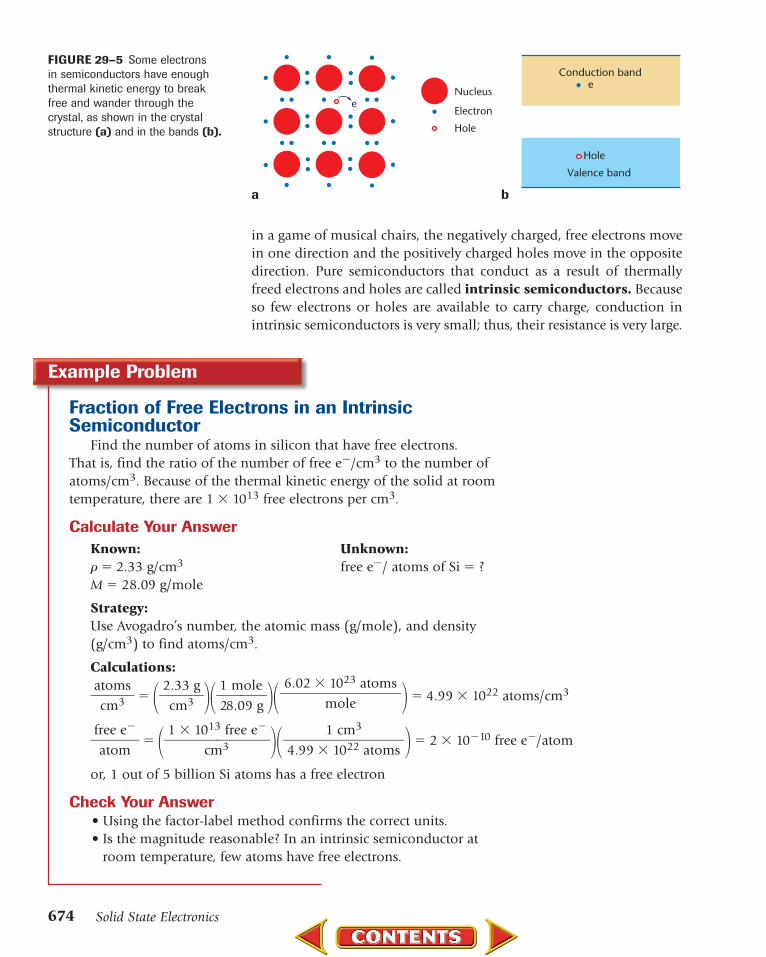
not as easily as in conductors, as shown in Figure 29–4b. The energy gapbetween the valence band and the conduction band is 1 eV or less. Howdoes the structure of a semiconductor explain its electronic characteristics?Atoms of the most common semiconductors, silicon (Si) and germanium(Ge), each have four valence electrons. These four electrons are involved inbinding the atoms together into the solid crystal. The valence electrons forma filled band, as in an insulator, but the forbidden gap between the valenceand conduction bands is much smaller than in an insulator. Not muchenergy is needed to pull one of the electrons from a silicon atom and put itinto the conduction band, as illustrated in Figure 29–5a. Indeed, the gap isso small that some electrons reach the conduction band as a result of theirthermal kinetic energy alone. That is, the random motion of atoms and elec-trons gives some electrons enough energy to break free of their home atomsand wander around the silicon crystal. If an electric field is applied to a semi-conductor, even more electrons are moved into the conduction band andmove through the solid according to the direction of the applied electricfield. In contrast to the effect in a metal, the higher the temperature of asemiconductor, the more electrons are able to reach the conduction band,and the higher the conductivity.
An atom from which an electron has broken free is missing an elec-tron and is said to contain a hole. As shown in Figure 29–5b, a hole isan empty energy level in the valence band. The atom now has a net pos-itive charge. If an electron breaks free from another atom, it can land onthe hole and become bound to an atom once again. When a hole and afree electron recombine, their opposite charges cancel each other. Theelectron, however, has left behind a hole on its previous atom. Thus, as
HELP WANTEDSYSTEMS ANALYSTIf you can analyze a prob-lem; select the best hardware,software, and support systemto solve it; and then workwith other staff members toimplement that solution, weare looking for you to fill asystems analyst position.
A B.S. or an advanceddegree in related areas, suchas business or scientific engi-neering, will determine yourposition within this boomingcomputer service company.Your sense of logic, ability tokeep up with advances in ourindustry, communicationskills, and willingness towork hard will determineyour success. For information contact:Association of InformationTechnology Professionals 315 South NorthwestHighway, Suite 200 Park Ridge, IL 60068-4278
FIGURE 29–4 Compare thevalence and conduction bands inan insulator (a) and in a semi-conductor (b). Notice that theforbidden gap is wider in a thanin b. Compare these diagramswith that shown in Figure 29–2.
29.1 Conduction in Solids 673
a b
Conduction band
Forbidden gapE ≈ 5 eV
Insulator
Valence band
Conduction band
Valence band
E ≈ 1 eV
Semiconductor
Fraction of Free Electrons in an Intrinsic Semiconductor
Find the number of atoms in silicon that have free electrons. That is, find the ratio of the number of free e/cm3 to the number ofatoms/cm3. Because of the thermal kinetic energy of the solid at roomtemperature, there are 1 1013 free electrons per cm3.
Calculate Your Answer Known: Unknown: 2.33 g/cm3 free e/ atoms of Si ?M 28.09 g/mole
Strategy:Use Avogadro’s number, the atomic mass (g/mole), and density(g/cm3) to find atoms/cm3.
Calculations:
a
c
to
m
m3s
2c
.3
m
33g
21
8
m
.0
o
9
le
g 4.99 1022 atoms/cm3
fr
a
e
t
e
om
e
1 10
c
1
m
3
3free e
2 1010 free e/atom
or, 1 out of 5 billion Si atoms has a free electron
Check Your Answer • Using the factor-label method confirms the correct units.• Is the magnitude reasonable? In an intrinsic semiconductor at
room temperature, few atoms have free electrons.
1 cm34.99 1022 atoms
6.02 1023 atoms
mole
674 Solid State Electronics
FIGURE 29–5 Some electrons in semiconductors have enoughthermal kinetic energy to breakfree and wander through the crystal, as shown in the crystalstructure (a) and in the bands (b).
Conduction bande
Nucleus
Electron
Hole
Valence band
e
Hole
in a game of musical chairs, the negatively charged, free electrons movein one direction and the positively charged holes move in the oppositedirection. Pure semiconductors that conduct as a result of thermallyfreed electrons and holes are called intrinsic semiconductors. Becauseso few electrons or holes are available to carry charge, conduction inintrinsic semiconductors is very small; thus, their resistance is very large.
a b
Example Problem

29.1 Conduction in Solids 675
Doped SemiconductorsAlthough conductivity does not depend only on the number of free
electrons, materials with fewer than one free electron per million atomswill not conduct electricity very well. To make a practical device, the con-ductivity of semiconductors must be increased greatly. This can be doneby adding certain other atoms, or impurities, which will create extrinsicsemiconductors. Impurity atoms, often called dopants, increase con-ductivity by adding either electrons or holes to a semiconductor.
n-type semiconductors There are two kinds of semiconductors:those that conduct by means of electrons, and those that conduct bymeans of holes. The type of semiconductor that conducts by means ofelectrons is called an n-type semiconductor because conduction is bymeans of negatively charged particles. Figure 29–6a shows how a fewdopant atoms replace silicon atoms in the crystal. Arsenic (As) atomsthat have five valence electrons can be used as a dopant. Four of the fiveelectrons bind to neighboring silicon atoms because silicon needs elec-trons to fill its valence band. The fifth electron is not needed in bond-ing and so can move relatively freely. This is called the donor electron.The energy of this donor electron is so close to the conduction band thatthermal energy can easily remove it from the impurity atom, putting anelectron in the conduction band, as shown in Figure 29–7a.
p-type semiconductors The type of semiconductor that conductsby means of holes is called a p-type semiconductor. What kind ofdopant atom can be used to create holes? A gallium (Ga) atom, for exam-ple, has only three valence electrons. If a gallium atom replaces a siliconatom, one binding electron is missing, as shown in Figure 29–6b. The
FIGURE 29–6 Donor atoms ofarsenic with five valence elec-trons replace acceptor atoms andprovide excess electrons in thesilicon crystal (a). Acceptoratoms of gallium with threevalence electrons create holes inthe crystal (b).
Excess electronfree to move4 4 4
4 5 4
4 4 4
Arsenic donor
Excess holefree to move
4 4 4
4 3 4
4 4 4
Gallium acceptor
a b
2. In pure germanium, density 5.23 g/cm3, atomic mass72.6 g/mole, there are 2 1016 free electrons/cm3 at room temperature. How many free electrons are there per atom?
Pocket LabAll Aboard!
Metals become better conduc-tors when they are cooled.Semiconductors become betterconductors when they areheated. Does a thermistor actlike a metal or a semiconductor?
Make a series circuit with alow-voltage DC power supply, a thermistor, and an ammeter(0-100 mA scale). Slowly turnup the power supply until theneedle is in the middle of thescale (50 mA). The voltage willbe about 0.6 V. Watch what hap-pens to the current when youhold the thermistor between yourfingers. Describe the results. Comparing and ContrastingList several possible advantagesof thermistors over standardthermometers.
Practice Problems

gallium atom is called an electron acceptor. That is, the gallium atomcreates a hole in the silicon semiconductor. Only thermal energy isneeded to excite electrons from the valence band into this hole creatinga hole on a silicon atom that is free to move through the crystal.Conduction is the result of the motion of positively charged holes in thevalence band, as shown in Figure 29–7b. Both p-type and n-type semi-conductors are electrically neutral. Adding dopant atoms of either typedoes not add any net charge to a semiconductor. If there are free elec-trons, then there are the same number of positively charged atoms.When a semiconductor conducts electricity by means of holes, there isa corresponding number of negatively charged atoms.
Silicon is doped by putting a silicon crystal in a vacuum with a sam-ple of the impurity material. The impurity material is heated until it isvaporized, and the atoms condense on the cold silicon. When the sili-con is warmed gently, the impurities diffuse into the material. Only afew impurity atoms per million silicon atoms are needed to increase theconductivity of the semiconductor by a factor of 1000 or more. Thus, theelectrical properties of a semiconductor can be determined by control-ling the number of impurity atoms doped into it. Finally, a thin layer ofaluminum or gold is evaporated on the crystal, and a wire is welded tothe conductor. The wire allows the user to put current into and bring itout of the doped silicon.
Thermistors The electrical conductivity of intrinsic and extrinsic semi-conductors is sensitive to both temperature and light. Unlike metals inwhich conductivity is reduced when the temperature rises, an increase intemperature of a semiconductor allows more electrons to reach the con-duction band. Thus, conductivity increases and resistance decreases. Onesemiconductor device, the thermistor, is designed so that its resistancedepends very strongly on temperature. Thus, the thermistor can be used asa sensitive thermometer and to compensate for temperature variations ofother components in an electrical circuit. Thermistors can also be used tomeasure the power of radio-frequency, infrared, and visible light sources.
676 Solid State Electronics
FIGURE 29–7 In an n-typesemiconductor, donor energy levels place electrons in the con-duction band (a). In a p-typesemiconductor, acceptor energylevels result in holes in thevalence band (b).
Conductionband
Forbiddengap
Valenceband
Electron
Hole
Donorimpuritylevels
Accepterimpuritylevels
Electron
Hole
a b
F.Y.I.Silicon circuits are nowbeing built on a layer ofsapphire crystal. Unlikesemiconductor bases thatallow some current to passthrough, the sapphire layeris nonconductive. Engineersmay now be able to putseveral integrated chips for a cellular phone on asingle chip.
67729.1 Conduction in Solids
The Conductivity of Doped SiliconSilicon is doped with arsenic so that one in every million Si atoms
is replaced by an arsenic atom. Each As atom donates one electron tothe conduction band. a. What is the density of free electrons? b. By what ratio is this density greater than that of intrinsic silicon
with 1 1013 free e/cm3? c. Is conduction mainly by the electrons of the silicon or the arsenic?
Calculate Your AnswerKnown: Unknown:1 As atom/106 Si atoms a. free e/cm3 donated by As1 free e/As atom b. ratio of As-donated free e to intrinsic free e
4.99 1022 Si atoms/cm3
1 1013 free e/cm3 in intrinsic Si
Strategy:From the density of Si atoms, find the density of As atoms. Becauseeach As atom donates one e, this number is the density of freeelectrons.
Calculations:
a. fr
c
e
m
e e3
11
A
fr
s
e
a
e
to
e
m1
1
1
A
0
s6
a
S
t
i
o
a
m
toms 4.99 1016 free e/cm3
b. Ratio is 4.99 103
c. Because there are 5000 arsenic-donated electrons for everyintrinsic electron, conduction is mainly by the arsenic-donatedelectrons.
Check Your Answer• Are the units correct? Using the factor-label method confirms the
correct units.• Is the magnitude reasonable? The ratio is large enough so that
intrinsic electrons make almost no contribution to conductivity.
4.99 1016 free e/cm3 in doped Si
1 1013 free e/cm3 in intrinsic Si
4.99 1022 Si atoms
cm3
3. If you wanted to have 5 103 as many electrons from As dopingas thermally free electrons in the germanium semiconductordescribed in Practice Problem 2, how many As atoms shouldthere be per Ge atom?
Example Problem
Practice Problems

678 Solid State Electronics
Section Review1. In which type of material, a conductor,
a semiconductor, or an insulator, areelectrons most likely to remain withthe same atom?
2. Magnesium oxide has a forbidden gapof 8 eV. Is this material a conductor,an insulator, or a semiconductor?
3. You are designing an integrated circuitusing a single crystal of silicon. Youwant to have a region with relativelygood insulating properties. Should you dope this region or leave it as anintrinsic semiconductor?
4. Evaluate the impact of semiconductorresearch on society.
5. Critical Thinking If the temperatureincreases, the number of free electronsin an intrinsic semiconductorincreases. For example, raising thetemperature by 10°C doubles thenumber of free electrons. Is it morelikely that an intrinsic semiconductoror a doped semiconductor will have a conductivity that depends on temperature? Explain.
29.1
Light meters Other useful applications of semiconductors depend ontheir light sensitivity. When light falls on a semiconductor, the light canexcite electrons from the valence band to the conduction band, in thesame way that light excites atoms. Thus, the resistance decreases as thelight intensity increases. Materials such as silicon and cadmium sulfideare used as light-dependent resistors in light meters used by astronomersto measure the brightness of stars; by lighting engineers to design theillumination of stores, offices, and homes; and by photographers to cap-ture the best image, as shown in Figure 29–8.
FIGURE 29–8 Photographerssometimes use a light meter tomeasure the intensity of incidentlight on an object. The meter con-verts the measurement into a unitthat tells the photographer whatexposure to set on the camera.

Today’s electronic instruments, such as radios, televisions,CD players, and microcomputers, often use semiconduc-
tor devices that are combined on chips of semiconductingsilicon a few millimeters wide. The chips contain not onlyregions of doped silicon that act as wires or resistors, butalso areas where two or three differently doped regions are
in contact. In these devices, current and voltage vary in more complexways than are described by Ohm’s law. Because the variation is not linear,the devices can change current from AC to DC and amplify voltages.
DiodesThe simplest semiconductor device is the diode. A diode consists of
joined regions of p-type and n-type semiconductors. Rather than twoseparate pieces of doped silicon being joined, a single sample of intrin-sic silicon is treated first with a p-dopant, then with an n-dopant. Metalcontacts are coated on each region so that wires can be attached, asshown in Figure 29–9. The boundary between the p-type and n-typeregions is called the junction. The resulting device therefore is called apn-junction diode.
The holes and electrons in the p- and n-regions are affected by thejunction. There are forces on the free-charge carriers in the two regionsnear the junction. The free electrons on the n-side are attracted to thepositive holes on the p-side. The electrons readily move into the p-sideand recombine with the holes. Holes from the p-side similarly move intothe n-side, where they recombine with electrons. As a result of this flow,the n-side has a net positive charge, and the p-side has a net negativecharge. These charges produce forces in the opposite direction that stopfurther movement of charge carriers. The region around the junction isleft with neither holes nor free electrons. This region, depleted of chargecarriers, is called the depletion layer. Because it has no charge carriers,it is a poor conductor of electricity. Thus, a junction diode consists of rel-atively good conductors at the ends that surround a poor conductor.
29.2Electronic Devices
OBJ ECTIVES:• Describe how diodes limit
current to motion in onlyone direction.
• Explain how a transistorcan amplify or increasevoltage changes.
29.2 Electronic Devices 679
FIGURE 29–9 A diagram of thepn junction diode shows thedepletion layer, where there areno charge carriers.
Metal p-type n-type Metal
Holes ElectronsJunction
Depletionlayer

680 Solid State Electronics
When a diode is connected into a circuit in the way shown in Figure 29–10a, both the free electrons in the n-type semiconductor andthe holes in the p-type semiconductor are attracted toward the battery.The width of the depletion layer is increased, and no charge carriersmeet. Almost no current flows through the diode: it acts like a very largeresistor, almost an insulator. A diode oriented in this manner is areverse-biased diode.
If the battery is connected in the opposite direction, as shown in Figure 29–10b, charge carriers are pushed toward the junction. If thevoltage of the battery is large enough, 0.6 V for a silicon diode, electronsreach the p-end and fill the holes. The depletion layer is eliminated, anda current flows. The battery continues to supply electrons for the n-end.It removes electrons from the p-end, which is the same as supplyingholes. With further increases in voltage from the battery, the currentincreases. A diode in this kind of circuit is a forward-biased diode.
The graph shown in Figure 29–11 indicates the current through a sil-icon diode as a function of voltage across it. If the applied voltage is neg-ative, the reverse-biased diode acts like a very high resistor; only a tinycurrent flows (about 1011 A for a silicon diode). If the voltage is posi-tive, the diode is forward-biased and acts like a small resistor, but not,however, one that obeys Ohm’s law. One major use of a diode is to con-vert AC voltage to a voltage that has only one polarity. When a diode isused in a circuit such as that illustrated in Figure 29–12, it is called arectifier. The arrow in the symbol for the diode shows the direction ofconventional current.
FIGURE 29–10 Compare thedirection of current in a reverse-biased diode (a) and a forward-biased diode (b).
FIGURE 29–11 The graphindicates current-voltagecharacteristics for a siliconjunction diode.
FIGURE 29–12 A diode can beused as a rectifier in a circuit.
p-type n-type
Holesfilled
Electronsleave
R
p-type n-type
Forward-biased diodeReverse-biased diode
New holescreated
Electrons andholes recombineat junction
New electronsadded
R
– + + –
I I
t t
Input voltage Output voltage
Rectified voltage
ACsource
Diode
R
25201510
50
–5–3 –2 –1 10
V (volts)
I(m
A)
Reversebias
Forwardbias
a b

29.2 Electronic Devices 681
A Diode in a Simple CircuitA silicon diode, with I/V characteristics like those shown in
Figure 29–11, is connected to a power supply through a 470- resistor.The power supply forward-biases the diode, and its voltage is adjusteduntil the diode current is 12 mA. What is the battery voltage?
Sketch the Problem• Draw a circuit diagram indicating the direction of current.
Calculate Your AnswerKnown: Unknown:
I 0.012 A Vb ?
Vd 0.7 V
R 470
Check Your Answer• Are the units correct? The battery’s potential difference is in volts.• Is the magnitude reasonable? Yes, it is larger than the diode
voltage drop, but less than 12 V, which is typical of batteries.
Calculations:
Vb IR Vd
Vb (0.012 A)(470 ) 0.7 V
6.3 V
Strategy:
The voltage drop across the resistor is knownfrom V IR, and this is the difference betweenthe battery voltage and the diode voltage drop.
Diodes can do more than provide one-way paths for current. Diodesmade from combinations of gallium and aluminum with arsenic andphosphorus emit light when they are forward-biased. When electronsreach the holes in the junction, they recombine and release the excessenergy at the wavelengths of light. These diodes are called light-emittingdiodes, or LEDs. Certain semiconductor crystals can be cut with parallelfaces so that the light waves reflect back and forth in the crystal. The
R
DiodeI
Vb
Vd
4. What battery voltage would be needed to produce a current of 2.5 mA in the diode in the preceding Example Problem?
5. A Ge diode has a voltage drop of 0.4 V when 12 mA flowthrough it. If the same 470- resistor is used, what battery voltage is needed?
Example Problem
Practice Problems

result is a diode laser that emits a narrow beam of coherent, monochro-matic light, or infrared radiation. Diode lasers are used in CD players andsupermarket bar-code scanners. They are compact, powerful light sources.
Both CD players and supermarket scanners must detect the laser lightreflected from the CD or bar code. Diodes can detect light as well asemit it. A reverse-biased pn-junction diode is usually used as a lightdetector. Light falling on the junction creates pairs of electrons andholes. These are pulled toward the ends of the diode, resulting in a cur-rent that depends on the light intensity.
Transistors and Integrated CircuitsA transistor is a simple device made of doped semiconducting mate-
rial that is used in most electronic circuits. One example of a transistorconsists of a region of one type of doped semiconductor sandwichedbetween layers of the opposite type. An npn transistor consists of n-typesemiconductors surrounding a thin p-type layer. If the center is an n-typeregion, then the device is called a pnp transistor. In either case, the cen-tral layer is called the base. The two surrounding regions are the emitterand the collector. The schematic symbols for the two transistor types areshown in Figure 29–13. The arrow is on the emitter and shows thedirection of conventional current.
The operation of an npn transistor is illustrated in Figure 29–14. Thepn-junctions in the transistor can be thought of as two back-to-backdiodes. The battery on the right keeps the potential difference betweencollector and emitter, VCE, positive. The base-collector diode is reverse-biased, so there is no current. The battery on the left is connected so thatthe base is more positive than the emitter. That is, the base-emitterdiode is forward-biased.
682 Solid State Electronics
FIGURE 29–13 Compare thecircuit symbols used to representa pnp transistor (a) and an npntransistor (b).
FIGURE 29–14 The circuit of annpn transistor demonstrates howvoltage can be amplified.
Circuit Symbols
Transistors
B
C
E
E E
B = base
pnp transistor npn transistor
C = collector E = emitter
p
p
n
n
n
p
B
BB
C
C C
E
BC
EVCE
VC
RC
RB
VB
IB
IC
a b
Pocket LabRed Light
Make a series circuit with apower supply, a 470- resistor,and a red LED. Connect theshort lead of the LED to thenegative side of the power supply. Attach the other lead tothe resistor. Hook the remainingresistor lead to the positive sideof the power supply. Slowlyincrease the voltage until theLED glows. Note the voltagesetting on the power supply. Hypothesize What will happenif you reverse the direction ofcurrent? Why? Try it and explainwhat happens.

29.2 Electronic Devices 683
A Revolution in RobotsAs our knowledge of solid state electronicsadvances, so does our ability to create smaller,more powerful computers called robots. Theessential characteristics of a robot include theability to be programmed to carry out asequence of actions and to repeat thoseactions over and over again, as instructed.
Robots for hazardous tasks Robots were first used for monotonous assembly-line tasks such as bolting togetherengine parts and handling molten metal.Now, they are used for work in hazardous orunusual environments. A robot rover calledPioneer, developed during the 1990s toclean toxic-waste storage tanks, helpeddecontaminate the damaged Chernobylnuclear reactor in Russia by locating radioactive hot spots and providing details of structural damage.
Robots as explorersUnlike humans, robots require no life-supportsystems, so they are less expensive to sendon interplanetary expeditions. The MarsSojourner rover was equipped with solar pan-els for power, wheels for travel, sensors andanalyzers for examining rocks and soil, andcommunications equipment for receivinginstructions from and sending data back tohuman operators on Earth.
MicrorobotsEngineers have discovered that tiny robotsare better than larger ones at handling tinycomponents, such as those used in the man-ufacture of electronic circuits. Microrobotshave also become very important in medi-cine. Because tiny instruments can be insertedinto the body through small incisions, they
reduce the pain and trauma of surgery. A sur-geon, viewing the body’s interior with aremote camera, can control the robot toremove a gall bladder or repair knee liga-ments. Some medical equipment is so pre-cise that it can more accurately manipulatetissues than the larger hand of a skilledhuman surgeon.
Robots even smaller than those currently inuse are in the works. Microtechnologists havecreated a working helicopter the size of apeanut. Some of its parts are a hundred timessmaller than the diameter of a human hair.Medical technologists and computer makersare among those keeping a close watch onthe microtechnology industry—an industrythat develops the microscopic structures usedin microdevices.
Investigating the Issue1. Using the Internet Search for information
about recent advances in artificial intelli-gence, then prepare to discuss the follow-ing questions. Has anyone invented arobot that can make human decisions? Do you think robots will ever be capableof human thought and emotions?
2. Thinking Critically Some researchers aretrying to develop robots that look and actlike humans. Would you prefer to workalongside a robot that looks like a machineor one that looks like a person? Why?
PHYSICSTo find out more about robots,visit the Glencoe Science Website at science.glencoe.com

684 Solid State Electronics
The StoplightProblem
How can you design a circuit so that changing the direction of the current changes the LED that lights up?
Materials0- to 12-V variable power supplyred LEDgreen LEDbicolored LEDwires470- resistorvoltmeter
Procedure1. Connect a series circuit with the power
supply, the resistor, and the red and greenLEDs to light them both. Do not bypass oromit the resistor with an LED. Always havethe resistor between an LED and one sideof the power supply.
2. Reverse the direction of the current in thecircuit and note the result. Measure thevoltage across an LED.
3. Design a circuit so that changing thedirection of the current will change the color that lights up.
4. Test your circuit.
5. When you have completed the lab, disposeof or recycle appropriate materials. Put awaymaterials that can be reused.
Data and Observations1. What voltage was needed to light the LEDs?
2. Describe what happened when the currentwas reversed.
Analyze and Conclude1. Diagramming a Circuit Make a drawing
to show your stoplight circuit (red on,green off; then green on, red off).
2. Explaining Results Why does your stoplight circuit work?
3. Analyzing Results Is your circuit aseries or parallel circuit?
4. Making Predictions What changewould you observe if you replaced theresistor with a 330- resistor?
5. Forming a Hypothesis If the voltageacross the LED was increased, what wouldhappen to the current?
6. Thinking Critically What must be truefor the graph of current vs. voltage to be a straight line?
Apply1. Design and conduct experiments to
discover what type of LED the bicoloredLED is. Remember to leave the resistorconnected to the power supply.
2. How does an LED differ from a 60-W lightbulb?

There is conventional current in the direction of the arrow from thebase into the emitter. Thus, electrons flow from the emitter into thebase. But the base layer is very thin, often less than 10–6 m wide. As aresult, most of the electrons pass through the base to the collector. Thecurrent through the collector, IC, is much larger than the currentthrough the base, IB. The collector current causes a voltage drop acrossresistor RC. Small changes in the voltage on the base produce largechanges in the collector current, and thus changes in the voltage dropacross RC. As a result, the transistor amplifies small voltage changes intomuch larger changes. A pnp transistor works the same way, except thatthe potentials of both batteries are reversed, and holes carry the currentin the transistor. The energy for amplification comes from the battery.
In a tape player, the small voltage variations from the voltage inducedin a coil by magnetized regions on the tape are amplified to move thespeaker coil. In computers, small currents in the base-emitter circuitscan turn on or turn off large currents in the collector-emitter circuits. Inaddition, several transistors can be connected together to perform logicoperations or to add numbers together. In this case, they act as fastswitches rather than as amplifiers.
Microchips An integrated circuit, or a microchip, consists of thou-sands of transistors, diodes, resistors, and conductors, each no morethan a few micrometers across. All these components can be made by dop-ing silicon, as shown in Figure 29–15. A microchip begins as an extremelypure single crystal of silicon, 10–20 cm in diameter and 1/2 m long. Thesilicon is sliced by a diamond-coated saw into wafers less than 1 mmthick. The circuit is then built layer by layer on the surface of this wafer.
68529.2 Electronic Devices
FIGURE 29–15 A piece of ultrapure silicon forms the basisfor an integrated circuit chip.
F.Y.I.Materials using micro-electromechanical systemsare almost sentient. Theycan “sense” changes intemperature, pressure, and motion. They are ableto actuate control mecha-nisms and communicate.Researchers foresee cloudsof these tiny machines monitoring hurricanes, performing medical proce-dures, and controllingmachine parts.
The Inside Dope Answers question from
page 668.

686 Solid State Electronics
Section Review1. Compare the resistance of a
pn-junction diode when it is forward-biased and reverse-biased.
2. In a light-emitting diode, which terminal should be connected to the p-end to make the diode light?
3. If the diode shown in Figure 29–11is forward-biased by a battery and aseries resistor so that there is morethan 10 mA of current, the voltagedrop is always about 0.7 V. Assume
that the battery voltage is increasedby 1 V.
a. By how much does the voltageacross the diode or the voltageacross the resistor increase?
b. By how much does the currentthrough the resistor increase?
4. Critical Thinking Could you replace an npn transistor with two separatediodes connected by their p-terminals?Explain.
29.2
By a photographic process, most of the wafer’s surface is covered by aprotective layer, with a pattern of selected areas left uncovered so that itcan be doped appropriately. The wafer is then placed in a vacuum chamber. Vapors of a dopant such as arsenic enter the machine, dopingthe wafer in the unprotected regions. By controlling the amount of expo-sure, the engineer can control the conductivity of the exposed regions ofthe chip. This process creates resistors, as well as one of the two layers ofa diode or one of the three layers of a transistor. The protective layer isremoved, and another one with a different pattern of exposed areas isapplied. Then the wafer is exposed to another dopant, often gallium, pro-ducing pn junctions. If a third layer is added, npn transistors are formed.The wafer also may be exposed to oxygen to produce areas of silicon diox-ide insulation. A layer exposed to aluminum vapors can produce a patternof thin conducting pathways among the resistors, diodes, and transistors.
Hundreds of identical circuits, usually called chips, are produced atone time on a single wafer with a 10– to 20–cm diameter. The chips arethen sliced apart and tested, attached to wires, and mounted in a plas-tic protective body. The tiny size of integrated circuits allows the place-ment of complicated circuits in a small space. Because electronic signalsneed to travel tiny distances, this miniaturization has increased thespeed of computers.
Semiconductor electronics requires that physicists, chemists, andengineers work together. Physicists contribute their understanding ofthe motion of electrons and holes in semiconductors. Physicists andchemists together add precisely controlled amounts of impurities toextremely pure silicon. Engineers develop the means of mass-producingchips containing thousands of miniaturized diodes and transistors.Together, their efforts have brought our world into this electronic age.

Chapter 29 Review 687
29.1 Conduction in Solids• Electrical conduction may be explained
by the band theory of solids.• In solids, the allowed energy levels are
spread into broad bands. The bands areseparated by regions called the forbid-den gaps, that is, by values of energiesthat electrons may not possess.
• In conductors, electrons can movebecause the valence band is only par-tially filled.
• Electrons in metals have a very fast ran-dom motion. A potential differenceacross the metal causes a very slow driftof the electrons.
• In insulators, more energy is needed tomove electrons than is generally available.
• Conduction in semi-conductors is usually the result of doping pure crystals with impurity atoms.
• n-type semiconductorsconduct by means of freeelectrons, and p-type semiconductorsconduct by means of holes.
29.2 Electronic Devices• Diodes conduct charges in one direc-
tion only and can be used to producecurrent in one direction only.
• A transistor has alternate layers of n-type and p-type semiconductors and can amplify voltage changes.
Key Terms
29.1• forbidden gap• band theory• valence band• conduction
band• hole• intrinsic
semiconductor• extrinsic
semiconductor• dopant• n-type
semiconductor• p-type
semiconductor
29.2• diode• pn-junction
diode• depletion layer• transistor
Summary
Reviewing ConceptsSection 29.11. How do the energy levels in a crystal
of an element differ from the energylevels in a single atom of that element?
2. Why does heating a semiconductorincrease its conductivity?
3. What is the main current carrier in ap-type semiconductor?
Section 29.24. An ohmmeter is an instrument that
places a potential difference across adevice to be tested, measures the cur-rent, and displays the resistance of thedevice. If you connect an ohmmeteracross a diode, will the current youmeasure depend on which end of thediode was connected to the positiveterminal of the ohmmeter? Explain.
5. What is the significance of the arrow-head at the emitter in a transistor circuit symbol?
6. Redraw Figure 29–14 as a pnptransistor.
Applying Concepts7. The resistance of graphite decreases
as temperature rises. Does graphiteconduct electricity like copper or like silicon?
8. Which of the following materialswould make a better insulator: onewith a forbidden gap 8 eV wide, onewith a forbidden gap 3 eV wide, orone with no forbidden gap?
9. Consider atoms of the three materialsin question 8. From which materialwould it be most difficult to removean electron?
10. How does the size of the gap betweenthe conduction band and the valenceband differ in semiconductors andinsulators?
11. Which would make a better insulator,an extrinsic or an intrinsic semicon-ductor? Explain.
12. Silicon is doped with phosphorus.Will the dopant atoms be donors oracceptors? Will the semiconductorconduct with holes or electrons?
CHAPTER 29 REVIEW

688 Solid State Electronics
CHAPTER 29 REVIEW
13. Doping silicon with gallium produces a p-typesemiconductor. Why are the holes mainly onthe silicon atoms rather than on the galliumatoms that caused the holes to be produced?
14. You use an ohmmeter to measure the resistanceof a pn-junction diode. Would the meter showa higher resistance when the diode is forward-biased or reverse-biased?
15. If the ohmmeter in problem 14 shows thelower resistance, is the ohmmeter lead con-nected to the arrow side of the diode at ahigher or lower potential than the lead con-nected to the other side?
16. If you dope pure germanium with gallium alone,do you produce a resistor, a diode, or a transistor?
ProblemsSection 29.1 17. The forbidden gap in silicon is 1.1 eV.
Electromagnetic waves striking the silicon causeelectrons to move from the valence band to theconduction band. What is the longest wave-length of radiation that could excite an electronin this way? Recall that
E 1240
eVnm
18. A light-emitting diode (LED) produces greenlight with a wavelength of 550 nm when anelectron moves from the conduction band tothe valence band. Find the width of the forbid-den gap in eV in this diode.
19. How many free electrons exist in a cubic centi-meter of sodium? Its density is 0.971 g/cm3, itsatomic mass is 22.99 g/mole, and there is onefree electron per atom.
20. At a temperature of 0°C, thermal energy frees1.1 1012 e/cm3 in pure silicon. The densityof silicon is 2.33 g/cm3, and the atomic massof silicon is 28.09 g/mole. What is the fractionof atoms that have free electrons?
21. Use the periodic table to determine which ofthe following elements could be added to ger-manium to make a p-type semiconductor: B, C,N, P, Si, Al, Ge, Ga, As, In, Sn, and Sb.
22. Which of the elements listed in problem 21would produce an n-type semiconductor?
Section 29.223. The potential drop across a glowing LED is
about 1.2 V. In Figure 29–16, the potentialdrop across the resistor is the differencebetween the battery voltage and the LED’spotential drop, 6.0 V 1.2 V 4.8 V. What isthe current througha. the LED? b. the resistor?
FIGURE 29–16
24. Jon wanted to raise the current through theLED in problem 23 up to 30 mA so that itwould glow brighter. Assume that the potentialdrop across the LED is still 1.2 V. What resistorshould be used?
25. Figure 29–17 shows a battery, diode, and bulbconnected in series so that the bulb lights. Notethat the diode is forward-biased. State whetherthe bulb in each of the pictured circuits, 1, 2,and 3, is lighted.
FIGURE 29–17
26. In the circuit shown in Figure 29–18, tellwhether lamp L1, lamp L2, both, or neither islighted.
27. A silicon diode whose I/V characteristics areshown in Figure 29–11 is connected to a batterythrough a 270- resistor. The battery forward-biases the diode, and its voltage is adjusted until the diode current is 15 mA. What is the battery voltage?
1 2 3
R = 240 Ω
Battery LED
V = 6.0 V
1.2 V

Chapter 29 Review 689
CHAPTER 29 REVIEW
FIGURE 29–18
28. What bulbs are lighted in the circuit shown inFigure 29–19 whena. switch 1 is closed and switch 2 is open?b. switch 2 is closed and switch 1 is open?
FIGURE 29–19
29. Which element or elements could be used asthe second dopant used to make a diode, if thefirst dopant were boron?
Critical Thinking Problems30. The I/V characteristics of two LEDs that glow
with different colors are shown in Figure 29–20.Each is to be connected through a resistor to a9.0-V battery. If each is to be run at a current of0.040 A, what resistors should be chosen for each?
31. Suppose that the two LEDs in problem 30 arenow connected in series. If the same battery isto be used and a current of 0.035 A is desired,what resistor should be used?
Going FurtherGraphing Data Planck’s constant can be esti-mated from an experiment with LEDs. To agood approximation, the voltage drop, V, acrossan LED depends on the frequency of light emis-sion, f, according to V = hf/e, where h is Planck’sconstant and e is the elementary charge. Asshown in Figure 29–11, however, the voltagedrop depends on current. To estimate Planck’sconstant, you have to measure the voltage whenthe current is very small, approximately 60 A.Obtain a collection of different-colored LEDs,from blue or green to infrared. Either measurethe wavelength of the light that they emit witha diffraction grating or prism spectrometer, orobtain the wavelength from the manufacturer’sdata tables. Compute the light frequency.Measure and plot the voltage drop as a functionof frequency. The slope of the line is h/e.Estimate Planck’s constant from the slope.
L1 L2
1 2
0.06
0.04
0.02
00 0.5 1 1.5 2 2.5 3
I (A
)
Voltage drop (V)FIGURE 29–20
L1 L2
PHYSICSTo review content, do the interactive quizzes on theGlencoe Science Web site atscience.glencoe.com
Extra Practice For more practice solving problems, go to Extra Practice Problems, Appendix B.