Embed Size (px)
Citation preview

designs
Article
The Impact of 3D Printing Process Parameters on theDielectric Properties of High Permittivity Composites
Athanasios Goulas 1,* , Shiyu Zhang 1 , Darren A. Cadman 1 , Jan Järveläinen 2,Ville Mylläri 2, Will G. Whittow 1 , John (Yiannis) C. Vardaxoglou 1 and Daniel S. Engstrøm 1
1 Wolfson School of Mechanical, Electrical & Manufacturing Engineering, Loughborough University,Loughborough, Leicestershire LE11 3TU, UK; [email protected] (S.Z.); [email protected] (D.A.C.);[email protected] (W.G.W.); [email protected] (J.(Y.)C.V.); [email protected] (D.S.E.)
2 Premix Oy, P.O. Box 12, FI-05201 Rajamäki, Finland; [email protected] (J.J.);[email protected] (V.M.)
* Correspondence: [email protected]
Received: 30 September 2019; Accepted: 4 November 2019; Published: 5 November 2019 �����������������
Abstract: Fused filament fabrication (FFF) is a well-known and greatly accessible additivemanufacturing technology, that has found great use in the prototyping and manufacture ofradiofrequency componentry, by using a range of composite thermoplastic materials that possesssuperior properties, when compared to standard materials for 3D printing. However, due to theirnature and synthesis, they are often a great challenge to print successfully which in turn affects theirmicrowave properties. Hence, determining the optimum printing strategy and settings is importantto advance this area. The manufacturing study presented in this paper shows the impact of the mainprocess parameters: printing speed, hatch spacing, layer height and material infill, during 3D printingon the relative permittivity (εr), and loss tangent (tanδ) of the resultant additively manufactured testsamples. A combination of process parameters arising from this study, allowed successful 3D printingof test samples, that marked a relative permittivity of 9.06 ± 0.09 and dielectric loss of 0.032 ± 0.003.
Keywords: 3D printing; artificial dielectrics; materials
1. Introduction
For more than two decades, polymers and their functional composites have received great attentiondue to their potential to be used in a variety of applications in electronics, such as piezo-resistive/electricdevices, conductors, etc. [1]. Polymers are typically materials of low relative permittivity or dielectricconstant (εr, where in order to increase their dielectric performance they are infilled with a highdielectric constant ceramic material (e.g., BaTiO3), in either a micro or nanoparticulate size, to form apolymer composite [2].
Such high dielectric performance polymer composites are of great use in the fabrication ofelectronic components and lately, they have attracted real interest, for their potential to be integratedinto modern radio-frequency (RF) devices operating at microwave frequencies [3]. Ceramic materialshave mostly been used in such applications due to their high dielectric constant and low dielectricloss [4], and an enormous amount of research and effort has been afforded for development of novelceramic materials [5]. However, production of ceramic components comes with several disadvantagessuch as high tooling costs and challenging implementation, since high temperature processing isrequired in order to achieve structural integrity and their desired dielectric properties.
Additive manufacturing (AM), commonly known as 3D printing, offers a great deal of flexibilityin the manufacture of complex three-dimensional geometries in near net-shape, eliminating any costsassociated with tooling and post-processing. Fused filament fabrication (FFF), belongs to the material
Designs 2019, 3, 50; doi:10.3390/designs3040050 www.mdpi.com/journal/designs
Designs 2019, 3, 50 2 of 10
extrusion process category, as defined in the ISO/DIS 17296 standard, in which a thermoplastic materialis drawn via a heated nozzle and deposits material in layer-by-layer manner to form three-dimensionalobjects. FFF is a particularly attractive 3D printing process, as it uses equipment of low complexityand it is relatively inexpensive. Despite it being only 30 years old, FFF has only recently becomevery popular in academia, especially during the past decade. One of the significant events was theexpiration of the FFF printing process patent in 2009, which led to a heavy decline in printer pricesand made them accessible to the larger public. The commercialization of printers has also boosted thedevelopment and commercialization of FFF filaments.
Previously high dielectric constant filaments have been made by stirring dissolved plastics withceramic particles. This is a time-consuming and expensive method and is nowadays commerciallyreplaced by melt compounding of the components. FFF filaments are typically made in two steps.First, a twin-screw extruder is used to compound the polymer, ceramic filler and various additives tomake plastic granules. Secondly, these granules are fed to a machine that makes the 3D-filaments. Thismachine typically contains a single-screw extruder, precision nozzle, cooling line, haul-off machineand a winder. Additionally, the line can also contain optical scanners to monitor the filament thicknessor material driers before the hopper, to achieve good dimensional accuracy.
Although 3D printing in general can be used to manufacture virtually anything, the rise of highpermittivity filaments has been mainly due to miniaturization of RF parts in the microwave region.One of the most typical applications where high permittivity filaments have been used is beamformingwith flat Fresnel zone or graded index lenses. A desirable lens form factor, i.e., a flat shape, can beachieved using the high permittivity material and varying the infill percentage to obtain an effective εr,
which varies radially along with the lens [6]. Benefits of high permittivity materials have also beendemonstrated in antennas [7,8], reflect arrays [9] and dielectric rod waveguides [10].
Very limited work has been reported to date, with regards to high permittivity polymer compositematerials suitable for FFF-type 3D printing. Castles et al. reported on the fabrication of a series ofcomposites composed of a BaTiO3/ABS polymer composite, which could be used with a commercialdesktop FFF-type 3D printer to produce parts containing user defined regions of relative permittivity.The authors reported polymer composite blends with ceramic solid loadings of up to 70 wt.%, relativepermittivity in the range of εr = 2.6–8.7 and loss tangents in the range of 0.005–0.027 [11]. Later on, Wuet al. presented an optimised blend, comprising of BaTiO3/ABS with volume ration of the infillingmaterial up to 32 vol.% and a maximum relative permittivity value of εr = 11, in the GHz frequencyrange [12]. To the best of our knowledge, the studies reported above, cover all the research activitiestaking place in producing high relative permittivity polymer composites for fused filament fabricationtype 3D printing.
However, it would seem that none of these studies have disseminated information with regardsto their printability or have investigated how processing conditions are likely to affect the performanceof the bulk printed materials. Since FFF has traditionally been used for prototyping purposes, andgiven its low level and low-cost nature, little attention has been given during the development of thetechnology to study and optimise the full density of the fabricated components. This is neverthelessexpected since FFF-made builds are not intended to be fully functional prototypes and process-relateddefects, such as porosity/air gaps are not considered important. This is not the case though fordielectric materials, since such imperfections can be detrimental to the performance of the fabricatedRF component.
In this work, we present a manufacturing study, using a high permittivity polymer compositefilament for FFF-type additive manufacturing. The resulting dielectric properties of the 3D printedsamples are assessed, according to the process-related parameters used, such as printing speed, hatchspacing, layer height and material infill.

Designs 2019, 3, 50 3 of 10
2. Materials and Methods
The experimental material used in this study was produced by Premix Oy (TP20907, Rajamäki,Finland) in filament form of 1.75 ± 0.1 mm diameter. It is a proprietary composite comprising of anacrylonitrile-butadiene-styrene (ABS) matrix, that contains a ceramic infill of a high relative permittivity.
All manufacturing experiments were carried out on a multi-process additive manufacturing kit(Hydra 16A, Hyrel3D, Norcross, GA, USA) equipped with a filament extrusion module (MK1-250,Hyrel3D, Norcross, GA, USA), fitted with a brass nozzle of 0.5 mm diameter. To assure better adhesionof the first layer, all test samples were printed on adhesive Kapton film of 75 µm thickness, that wasplaced on top of build surface, heated at 110 ◦C.
The composite thermoplastic filament was subjected to differential scanning calorimetry (DSC)(2920 Modulated DSC, TA Instruments Inc., New Castle, DE, USA), to identify the thermophysicalproperties of the material, such as glass transition, decomposition temperature and any otherthermophysical material interactions during heating. Those properties helped to identify processingconditions such as the temperature of the build surface and extrusion. DSC was operated under anargon gas environment with a 200 mL/min−1 purging rate, at a heating rate of 10 ◦C·min−1 from roomtemperature up to 350 ◦C. All samples were introduced in high purity aluminium pans with an emptypan used as a reference to calibrate the baseline.
The morphological features of the 3D printed structures, such as internal porosity were investigatedusing light optical microscopy (LOM) (Eclipse MA200, Nikon Instruments Europe, Netherlands), wherethe dispersion of the ceramic infilling material into the thermoplastic host was depicted using scanningelectron microscopy (SEM) (TM3030 SEM, Hitachi High-Technologies Europe GmbH, Germany). SEMsamples were coated with a gold/palladium alloy in an 80:20 weight ratio, for 90 s at 25 mA using asputter coater (Quorum Q150T, Quorum, Edwards, Hastings, UK).
The dielectric properties of the additively manufactured samples were determined by placingthe printed samples of 22.86 × 10.16 × 2.5 mm size, into an X-band waveguide cavity (8.2–12.4 GHz),measuring the transmission and reflection from the target sample, connected to a Vector NetworkAnalyser (VNA) (MS465B22, Anritsu, Japan) using coaxial cables. Relative permittivity (εr) and losstangent (tanδ) were calculated using the Nicolson-Ross-Weir method [13]. All reported measurementsare reported as an average out of 5 different 3D printed samples together with standard error.
3. Results and Discussion
Depending on the percentage amount of the infilling material, composites typically exhibitproperties such as glass transition or decomposition that are very different to the properties of the hostmaterial. According to the manufacturer, this experimental material in these studies that came in theform of a filament suitable for FFF, is a proprietary blend based on an ABS host and contained a highdielectric constant ceramic infill in nanoparticulate form, as shown in Figure 1.
The material was initially subjected to thermal analysis using Differential Scanning Calorimetry(DSC) to identify its thermal behaviour and extract information critical for the successful manufactureof three-dimensional test samples. Calorimetric data revealed a glass transition (Tg) reaction at 105 ◦Cand a major endothermic peak at 290 ◦C, suggesting complete melting (Tm), as seen in Figure 2.
For thermoplastics, the glass transition (Tg) is the temperature range where the material undergoesa viscous relaxation and behaves as it is in a glassy state; it is strong and rigid but also soft and pliablewhen it is below the glass transition [14]. In 3D printing of thermoplastics, a temperature slightlyabove the material’s Tg is typically used for heating the built platform. This enables the material toadhere better to the surface, as it leads to a reduction of the surface tension between the printingsurface and the printed material, and to a larger contact area that ultimately will cause better adhesionbetween the bed and the extrudate [15]. Additionally, the build platform’s temperature will not allowthe extrudate to cool down below its glass transition thereby allowing it to mechanically interlockto the surface characteristics of the build surface, such as porosity and roughness, ensuring properadherence. A value of 110 ◦C, corresponding to a temperature slightly above the material’s Tg = 105

Designs 2019, 3, 50 4 of 10
◦C, was chosen as the temperature setting for the equipment’s build surface and was similar to mostABS thermoplastic blends typically used for 3D printing.Designs 2019, 3, x FOR PEER REVIEW 4 of 10
Figure 1. Scanning electron micrograph of the ceramic infill nanoparticles within an ABS matrix.
The material was initially subjected to thermal analysis using Differential Scanning Calorimetry
(DSC) to identify its thermal behaviour and extract information critical for the successful
manufacture of three‐dimensional test samples. Calorimetric data revealed a glass transition (Tg)
reaction at 105 °C and a major endothermic peak at 290 °C, suggesting complete melting (Tm), as seen
in Figure 2.
0 50 100 150 200 250 300 350
Temperature (°C)
-0.4
-0.35
-0.3
-0.25
-0.2
TP20907
X: 290Y: -0.3767
X: 105Y: -0.3336
Figure 2. DSC curve of Premix PREPERM™ TP20907.
For thermoplastics, the glass transition (Tg) is the temperature range where the material
undergoes a viscous relaxation and behaves as it is in a glassy state; it is strong and rigid but also soft
and pliable when it is below the glass transition [14]. In 3D printing of thermoplastics, a temperature
slightly above the material’s Tg is typically used for heating the built platform. This enables the
material to adhere better to the surface, as it leads to a reduction of the surface tension between the
printing surface and the printed material, and to a larger contact area that ultimately will cause
better adhesion between the bed and the extrudate [15]. Additionally, the build platform’s
temperature will not allow the extrudate to cool down below its glass transition thereby allowing it
to mechanically interlock to the surface characteristics of the build surface, such as porosity and
roughness, ensuring proper adherence. A value of 110 °C, corresponding to a temperature slightly
Figure 1. Scanning electron micrograph of the ceramic infill nanoparticles within an ABS matrix.
Designs 2019, 3, x FOR PEER REVIEW 4 of 10
Figure 1. Scanning electron micrograph of the ceramic infill nanoparticles within an ABS matrix.
The material was initially subjected to thermal analysis using Differential Scanning Calorimetry
(DSC) to identify its thermal behaviour and extract information critical for the successful
manufacture of three‐dimensional test samples. Calorimetric data revealed a glass transition (Tg)
reaction at 105 °C and a major endothermic peak at 290 °C, suggesting complete melting (Tm), as seen
in Figure 2.
0 50 100 150 200 250 300 350
Temperature (°C)
-0.4
-0.35
-0.3
-0.25
-0.2
TP20907
X: 290Y: -0.3767
X: 105Y: -0.3336
Figure 2. DSC curve of Premix PREPERM™ TP20907.
For thermoplastics, the glass transition (Tg) is the temperature range where the material
undergoes a viscous relaxation and behaves as it is in a glassy state; it is strong and rigid but also soft
and pliable when it is below the glass transition [14]. In 3D printing of thermoplastics, a temperature
slightly above the material’s Tg is typically used for heating the built platform. This enables the
material to adhere better to the surface, as it leads to a reduction of the surface tension between the
printing surface and the printed material, and to a larger contact area that ultimately will cause
better adhesion between the bed and the extrudate [15]. Additionally, the build platform’s
temperature will not allow the extrudate to cool down below its glass transition thereby allowing it
to mechanically interlock to the surface characteristics of the build surface, such as porosity and
roughness, ensuring proper adherence. A value of 110 °C, corresponding to a temperature slightly
Figure 2. DSC curve of Premix PREPERM™ TP20907.
Most amorphous thermoplastic materials such as ABS do not have a sharply defined meltingtemperature; they exist in a melt state past their glass transition, but their viscosity is too high to allowfor any flow, or any extrusion, as in the case of FFF-type 3D printing. As the material becomes heated,the viscosity reduces significantly, up to a point where the viscosity is low enough to facilitate flow.
DSC data showed a continuous decomposition up to a temperature of 290 ◦C correspondingto the maximum of the endothermic peak. This suggested that extrusion temperature should notexceed 290 ◦C to avoid unwanted process repercussions, such as uncontrolled melting and degradationof the thermoplastic polymer. A series of trials, extruding with temperatures below that of 290 ◦C,determined that 260 ◦C was the best suited temperature, allowing smooth, continuous and in the overall
Designs 2019, 3, 50 5 of 10
defect-free extrusion of the composite material. It should be noted that the extrusion temperature usedwas unusually high, since ABS-based materials are typically 3D printed using process temperaturesbetween 230–240 ◦C. This suggested that the amount of the infilling ceramic material had a significantimpact on the material’s thermal properties and thus on its processability. The higher the solid loading,the higher the viscosity of the composite, therefore higher extrusion temperatures were needed toallow melt flow.
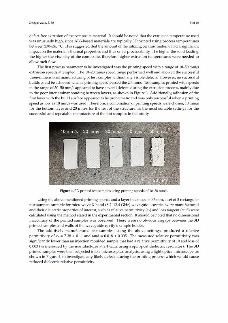
The first process parameter to be investigated was the printing speed with a range of 10–50 mm/sextrusion speeds attempted. The 10–20 mm/s speed range performed well and allowed the successfulthree-dimensional manufacturing of test samples without any visible defects. However, no successfulbuilds could be achieved when a printing speed passed the 20 mm/s. Test samples printed with speedsin the range of 30–50 mm/s appeared to have several defects during the extrusion process, mainly dueto the poor interlaminar bonding between layers, as shown in Figure 3. Additionally, adhesion of thefirst layer with the build surface appeared to be problematic and was only successful when a printingspeed as low as 10 mm/s was used. Therefore, a combination of printing speeds were chosen, 10 mm/sfor the bottom layer and 20 mm/s for the rest of the structure, as the most suitable settings for thesuccessful and repeatable manufacture of the test samples in this study.
Designs 2019, 3, x FOR PEER REVIEW 5 of 10
above the material’s Tg = 105 °C, was chosen as the temperature setting for the equipment’s build
surface and was similar to most ABS thermoplastic blends typically used for 3D printing.
Most amorphous thermoplastic materials such as ABS do not have a sharply defined melting
temperature; they exist in a melt state past their glass transition, but their viscosity is too high to
allow for any flow, or any extrusion, as in the case of FFF‐type 3D printing. As the material becomes
heated, the viscosity reduces significantly, up to a point where the viscosity is low enough to
facilitate flow.
DSC data showed a continuous decomposition up to a temperature of 290 °C corresponding to
the maximum of the endothermic peak. This suggested that extrusion temperature should not
exceed 290 °C to avoid unwanted process repercussions, such as uncontrolled melting and
degradation of the thermoplastic polymer. A series of trials, extruding with temperatures below that
of 290 °C, determined that 260 °C was the best suited temperature, allowing smooth, continuous and
in the overall defect‐free extrusion of the composite material. It should be noted that the extrusion
temperature used was unusually high, since ABS‐based materials are typically 3D printed using
process temperatures between 230–240 °C. This suggested that the amount of the infilling ceramic
material had a significant impact on the material’s thermal properties and thus on its processability.
The higher the solid loading, the higher the viscosity of the composite, therefore higher extrusion
temperatures were needed to allow melt flow.
The first process parameter to be investigated was the printing speed with a range of 10–50
mm/s extrusion speeds attempted. The 10–20 mm/s speed range performed well and allowed the
successful three‐dimensional manufacturing of test samples without any visible defects. However,
no successful builds could be achieved when a printing speed passed the 20 mm/s. Test samples
printed with speeds in the range of 30–50 mm/s appeared to have several defects during the
extrusion process, mainly due to the poor interlaminar bonding between layers, as shown in Figure
3. Additionally, adhesion of the first layer with the build surface appeared to be problematic and
was only successful when a printing speed as low as 10 mm/s was used. Therefore, a combination of
printing speeds were chosen, 10 mm/s for the bottom layer and 20 mm/s for the rest of the structure,
as the most suitable settings for the successful and repeatable manufacture of the test samples in this
study.
Figure 3. 3D printed test samples using printing speeds of 10–50 mm/s.
Using the above‐mentioned printing speeds and a layer thickness of 0.3 mm, a set of 5
rectangular test samples suitable for microwave X‐band (8.2–12.4 GHz) waveguide cavities were
manufactured and their dielectric properties of interest, such as relative permittivity (εr) and loss
tangent (tanδ) were calculated using the method stated in the experimental section. It should be
noted that no dimensional inaccuracy of the printed samples was observed. There were no obvious
airgaps between the 3D printed samples and walls of the waveguide cavity’s sample holder.
The additively manufactured test samples, using the above settings, produced a relative
permittivity of εr = 7.38 ± 0.11 and tanδ = 0.018 ± 0.005. The measured relative permittivity was
Figure 3. 3D printed test samples using printing speeds of 10–50 mm/s.
Using the above-mentioned printing speeds and a layer thickness of 0.3 mm, a set of 5 rectangulartest samples suitable for microwave X-band (8.2–12.4 GHz) waveguide cavities were manufacturedand their dielectric properties of interest, such as relative permittivity (εr) and loss tangent (tanδ) werecalculated using the method stated in the experimental section. It should be noted that no dimensionalinaccuracy of the printed samples was observed. There were no obvious airgaps between the 3Dprinted samples and walls of the waveguide cavity’s sample holder.
The additively manufactured test samples, using the above settings, produced a relativepermittivity of εr = 7.38 ± 0.11 and tanδ = 0.018 ± 0.005. The measured relative permittivity wassignificantly lower than an injection moulded sample that had a relative permittivity of 10 and loss of0.003 (as measured by the manufacturer at 2.4 GHz using a split-post dielectric resonator). The 3Dprinted samples were then subjected into a microscopical analysis, using a light optical microscope, asshown in Figure 4, to investigate any likely defects during the printing process which would causereduced dielectric relative permittivity.

Designs 2019, 3, 50 6 of 10
Designs 2019, 3, x FOR PEER REVIEW 6 of 10
significantly lower than an injection moulded sample that had a relative permittivity of 10 and loss
of 0.003 (as measured by the manufacturer a
Figure 4. Optical micrograph showing the density of 3D printed samples using (a) 0.5 mm extrusion
width versus (b) 0.45 mm extrusion width.
The acquired optical micrographs showed that there was an air gap, in between the individual
printed lines forming a single layer. This is shown by the arrow in Figure 4a. This clearly explained
the inferior performance in terms of the measured relative permittivity against the bulk material
properties, since any voids or air gaps were expected to reduce the measured relative permittivity of
the material. The reason for the presence of such air gaps were likely to be caused either: a) due to
significant material shrinkage during the cooling down phase of the extrudate, or b) due to
non‐optimal material flow, which is normally controlled by the software responsible for generating
the extrusion parameters during slicing and generation of the g‐code. In the first case, this is likely to
be the effect of a high solid loading of the ceramic material, affecting the thermophysical properties
of the composite. For the latter case, such differences in the extrusion output can be software specific.
The algorithm responsible for generating the extrusion parameters in the g‐code might differ
between the software package used (i.e., Simplify3D, Slic3r, Cura, etc.).
In order to compensate for the above‐mentioned shortcoming, the extrusion width that controls
the distance between the individual printed lines forming the monolayer was reduced from 0.5 mm
to 0.45 mm. This 0.05 mm reduction in the extrusion width matched the dimension of the air gaps, as
measured using the previously acquired optical micrographs, as shown in Figure 4. Material flow
rate multiplayer was left unchanged from its default value of 1, as it would drastically change the
amount of material being extruded per given layer thickness and would likely cause over‐extrusion,
and result in swelling/oozing of the final three‐dimensionally printed geometry.
A new set of samples were manufactured, using the adjusted extrusion width value of 0.45 mm
and were subsequently measured in the X‐band waveguide cavity. Their properties showed a
slightly higher relative permittivity and also a lower loss tangent, with values of εr = 7.85 ± 0.25, and
tanδ = 0.008 ± 0.011, as shown in Figure 5. This is clearly explained due to the reduction of any
airgaps existing in the continuity of a monolayer. The latter was confirmed by acquiring optical
micrographs as shown in Figure 4b. The minor variance in the dielectric performance of the 3D
printed samples, as depicted via the error bars, was very likely to be due to inconsistencies during
extrusion.
Figure 4. Optical micrograph showing the density of 3D printed samples using (a) 0.5 mm extrusionwidth versus (b) 0.45 mm extrusion width.
The acquired optical micrographs showed that there was an air gap, in between the individualprinted lines forming a single layer. This is shown by the arrow in Figure 4a. This clearly explained theinferior performance in terms of the measured relative permittivity against the bulk material properties,since any voids or air gaps were expected to reduce the measured relative permittivity of the material.The reason for the presence of such air gaps were likely to be caused either: a) due to significantmaterial shrinkage during the cooling down phase of the extrudate, or b) due to non-optimal materialflow, which is normally controlled by the software responsible for generating the extrusion parametersduring slicing and generation of the g-code. In the first case, this is likely to be the effect of a high solidloading of the ceramic material, affecting the thermophysical properties of the composite. For the lattercase, such differences in the extrusion output can be software specific. The algorithm responsible forgenerating the extrusion parameters in the g-code might differ between the software package used (i.e.,Simplify3D, Slic3r, Cura, etc.).
In order to compensate for the above-mentioned shortcoming, the extrusion width that controlsthe distance between the individual printed lines forming the monolayer was reduced from 0.5 mm to0.45 mm. This 0.05 mm reduction in the extrusion width matched the dimension of the air gaps, asmeasured using the previously acquired optical micrographs, as shown in Figure 4. Material flow ratemultiplayer was left unchanged from its default value of 1, as it would drastically change the amountof material being extruded per given layer thickness and would likely cause over-extrusion, and resultin swelling/oozing of the final three-dimensionally printed geometry.
A new set of samples were manufactured, using the adjusted extrusion width value of 0.45 mmand were subsequently measured in the X-band waveguide cavity. Their properties showed a slightlyhigher relative permittivity and also a lower loss tangent, with values of εr = 7.85 ± 0.25, and tanδ= 0.008 ± 0.011, as shown in Figure 5. This is clearly explained due to the reduction of any airgapsexisting in the continuity of a monolayer. The latter was confirmed by acquiring optical micrographsas shown in Figure 4b. The minor variance in the dielectric performance of the 3D printed samples, asdepicted via the error bars, was very likely to be due to inconsistencies during extrusion.
Designs 2019, 3, 50 7 of 10Designs 2019, 3, x FOR PEER REVIEW 7 of 10
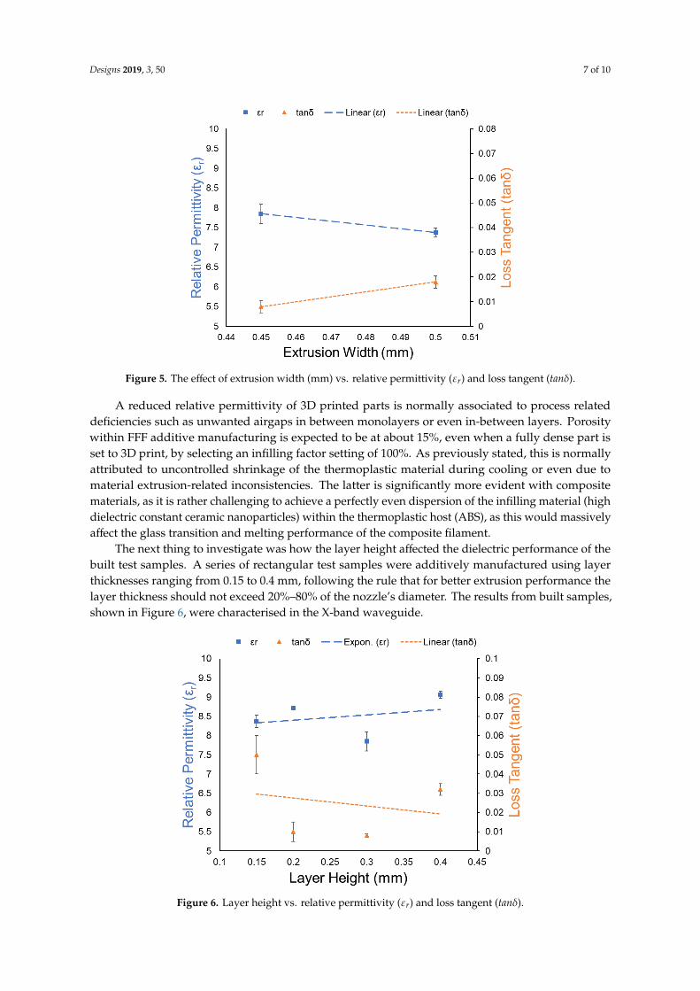
Figure 5. The effect of extrusion width (mm) vs. relative permittivity (εr) and loss tangent (tanδ).
A reduced relative permittivity of 3D printed parts is normally associated to process related
deficiencies such as unwanted airgaps in between monolayers or even in‐between layers. Porosity
within FFF additive manufacturing is expected to be at about 15%, even when a fully dense part is
set to 3D print, by selecting an infilling factor setting of 100%. As previously stated, this is normally
attributed to uncontrolled shrinkage of the thermoplastic material during cooling or even due to
material extrusion‐related inconsistencies. The latter is significantly more evident with composite
materials, as it is rather challenging to achieve a perfectly even dispersion of the infilling material
(high dielectric constant ceramic nanoparticles) within the thermoplastic host (ABS), as this would
massively affect the glass transition and melting performance of the composite filament.
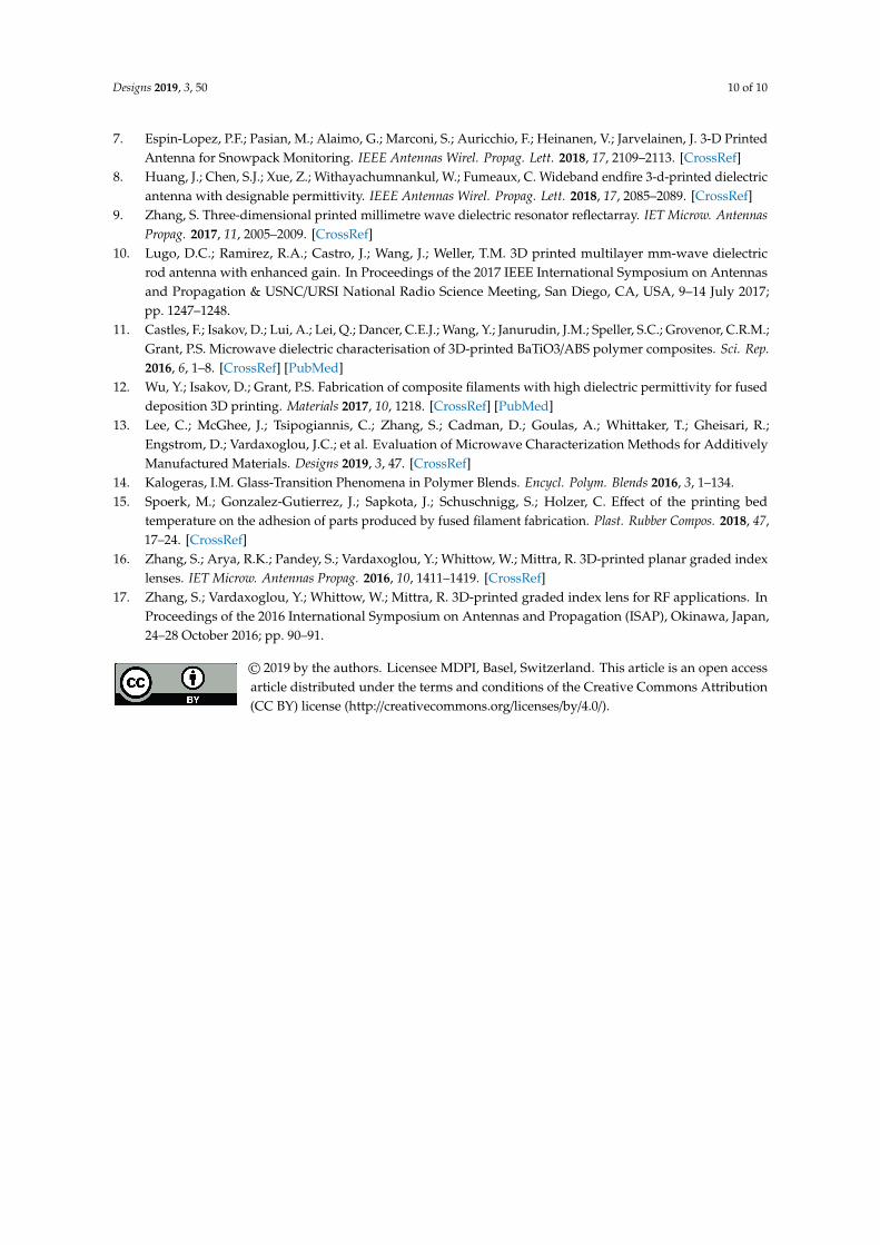
The next thing to investigate was how the layer height affected the dielectric performance of the
built test samples. A series of rectangular test samples were additively manufactured using layer
thicknesses ranging from 0.15 to 0.4 mm, following the rule that for better extrusion performance the
layer thickness should not exceed 20%–80% of the nozzle’s diameter. The results from built samples,
shown in Figure 6, were characterised in the X‐band waveguide.
Figure 6. Layer height vs. relative permittivity (εr) and loss tangent (tanδ).
Figure 5. The effect of extrusion width (mm) vs. relative permittivity (εr) and loss tangent (tanδ).
A reduced relative permittivity of 3D printed parts is normally associated to process relateddeficiencies such as unwanted airgaps in between monolayers or even in-between layers. Porositywithin FFF additive manufacturing is expected to be at about 15%, even when a fully dense part isset to 3D print, by selecting an infilling factor setting of 100%. As previously stated, this is normallyattributed to uncontrolled shrinkage of the thermoplastic material during cooling or even due tomaterial extrusion-related inconsistencies. The latter is significantly more evident with compositematerials, as it is rather challenging to achieve a perfectly even dispersion of the infilling material (highdielectric constant ceramic nanoparticles) within the thermoplastic host (ABS), as this would massivelyaffect the glass transition and melting performance of the composite filament.
The next thing to investigate was how the layer height affected the dielectric performance of thebuilt test samples. A series of rectangular test samples were additively manufactured using layerthicknesses ranging from 0.15 to 0.4 mm, following the rule that for better extrusion performance thelayer thickness should not exceed 20%–80% of the nozzle’s diameter. The results from built samples,shown in Figure 6, were characterised in the X-band waveguide.
Designs 2019, 3, x FOR PEER REVIEW 7 of 10
Figure 5. The effect of extrusion width (mm) vs. relative permittivity (εr) and loss tangent (tanδ).
A reduced relative permittivity of 3D printed parts is normally associated to process related
deficiencies such as unwanted airgaps in between monolayers or even in‐between layers. Porosity
within FFF additive manufacturing is expected to be at about 15%, even when a fully dense part is
set to 3D print, by selecting an infilling factor setting of 100%. As previously stated, this is normally
attributed to uncontrolled shrinkage of the thermoplastic material during cooling or even due to
material extrusion‐related inconsistencies. The latter is significantly more evident with composite
materials, as it is rather challenging to achieve a perfectly even dispersion of the infilling material
(high dielectric constant ceramic nanoparticles) within the thermoplastic host (ABS), as this would
massively affect the glass transition and melting performance of the composite filament.
The next thing to investigate was how the layer height affected the dielectric performance of the
built test samples. A series of rectangular test samples were additively manufactured using layer
thicknesses ranging from 0.15 to 0.4 mm, following the rule that for better extrusion performance the
layer thickness should not exceed 20%–80% of the nozzle’s diameter. The results from built samples,
shown in Figure 6, were characterised in the X‐band waveguide.
Figure 6. Layer height vs. relative permittivity (εr) and loss tangent (tanδ). Figure 6. Layer height vs. relative permittivity (εr) and loss tangent (tanδ).

Designs 2019, 3, 50 8 of 10
As shown in Figure 6, both the relative permittivity and loss tangent values showed a correlationwith the varying changing layer height. For a layer height setting of 0.15 mm, dielectric properties ofεr = 8.37 ± 0.16 and tanδ = 0.05 ± 0.001 were measured. However, samples built with a thicker layerheight of 0.4 mm demonstrated a higher relative permittivity and lower loss: with dielectric propertyvalues as high as εr = 9.06 ± 0.09 and tanδ = 0.032 ± 0.003. These results are closely comparable tothe bulk material’s measured properties, as manufactured via injection moulding, that were εr = 10and tanδ = 0.003. This increased relative permittivity was due to a combination of reasons, such asthe reduction of overall porosity within the sample’s volume together with the increased amount ofextruded material per given layer height.
It has previously been reported by Zhang et al. that by controlling the amount of the materialinfill during a print, the relative permittivity could be effectively controlled. This could allow for themanufacture of complex substrates that has locally tailored varied relative permittivity for advancedRF component design [16]. Therefore, a study was carried out to investigate the degree of freedomin controlling the relative permittivity of printed geometries with varied infill factors by using theTP20907 composite ABS, as shown in Figure 7.
Designs 2019, 3, x FOR PEER REVIEW 8 of 10
As shown in Figure 6, both the relative permittivity and loss tangent values showed a
correlation with the varying changing layer height. For a layer height setting of 0.15 mm, dielectric
properties of εr = 8.37 ± 0.16 and tanδ = 0.05 ± 0.001 were measured. However, samples built with a
thicker layer height of 0.4 mm demonstrated a higher relative permittivity and lower loss: with
dielectric property values as high as εr = 9.06 ± 0.09 and tanδ = 0.032 ± 0.003. These results are closely
comparable to the bulk material’s measured properties, as manufactured via injection moulding,
that were εr = 10 and tanδ = 0.003. This increased relative permittivity was due to a combination of
reasons, such as the reduction of overall porosity within the sample’s volume together with the
increased amount of extruded material per given layer height.
It has previously been reported by Zhang et al. that by controlling the amount of the material
infill during a print, the relative permittivity could be effectively controlled. This could allow for the
manufacture of complex substrates that has locally tailored varied relative permittivity for advanced
RF component design [16]. Therefore, a study was carried out to investigate the degree of freedom in
controlling the relative permittivity of prin
Figure 7. (a) Material Infill (%) vs. relative permittivity (εr) and loss tangent (tanδ), (b) Examples of
built test samples with variable material infill.
A set of test samples, using infill settings, corresponding to the range of 20%–100% were built.
Like the previous process parameters, the infill rate was controlled via the 3D printer’s native
software. For clarification, a 20% material infill setting translates to a final geometry of a given
volume, that the deposited material accounts for 20% of its overall volume, as shown in Figure 7. The
remaining 80% consists of air gaps. It should be noted that interlayer adhesion was very poor when a
material infill setting below 20% was chosen and resulted in inferior interlayer adhesion compared
with the same partial infilled ABS geometry. This did not allow for the manufacture of any test
specimens with infill less than 20%.
Results plotted in Figure 7, demonstrated a clear correlation of the infill factor against the
measured relative permittivity (εr). It was also noted that the reduction in the material infill has a
positive effect on the material’s losses. The minimum infill setting of 20% led to a relative
permittivity of εr = 2.164 ± 0.04 and loss tangent tanδ = 0.02 ± 0.002. More advanced RF components,
such as planar graded index dielectric lenses [16,17], require a range of dielectric materials with
precise specifications which are not commercially available. The above presented approach lends
itself to a quick and cost‐effective way to produce dielectric materials with bespoke relative
permittivity values.
Figure 7. (a) Material Infill (%) vs. relative permittivity (εr) and loss tangent (tanδ), (b) Examples ofbuilt test samples with variable material infill.
A set of test samples, using infill settings, corresponding to the range of 20%–100% were built.Like the previous process parameters, the infill rate was controlled via the 3D printer’s native software.For clarification, a 20% material infill setting translates to a final geometry of a given volume, that thedeposited material accounts for 20% of its overall volume, as shown in Figure 7. The remaining 80%consists of air gaps. It should be noted that interlayer adhesion was very poor when a material infillsetting below 20% was chosen and resulted in inferior interlayer adhesion compared with the samepartial infilled ABS geometry. This did not allow for the manufacture of any test specimens with infillless than 20%.
Results plotted in Figure 7, demonstrated a clear correlation of the infill factor against the measuredrelative permittivity (εr). It was also noted that the reduction in the material infill has a positiveeffect on the material’s losses. The minimum infill setting of 20% led to a relative permittivity ofεr = 2.164 ± 0.04 and loss tangent tanδ = 0.02 ± 0.002. More advanced RF components, such as planargraded index dielectric lenses [16,17], require a range of dielectric materials with precise specificationswhich are not commercially available. The above presented approach lends itself to a quick andcost-effective way to produce dielectric materials with bespoke relative permittivity values.

Designs 2019, 3, 50 9 of 10
4. Conclusions
FFF is a common and widely adopted 3D printing technology that can also potentially be usedfor rapid manufacture of functional prototypes for telecommunication and microwave/RF devices.This can be achieved by using composite thermoplastic materials that possess superior dielectricproperties, such as: higher relative permittivity (εr) and low loss (tanδ), that are hardly realised byconventional thermoplastics. However, the electromagnetic properties of those 3D printed parts areoften not comparable to the properties of the bulk material, due to process-related deficiencies subject ofthe printing parameters being used. The major findings of this paper are summarised in the followingbullet points:
• Printing speed was found to have a direct effect on the interlaminar bonding of the 3D printedtest samples. It is important to use slower printing speeds with composite thermoplastics, sincethe ceramic solid infill affects the extrudability of the material. A combination of 10 mm/s forthe bottom layer and 20 mm/s for the rest of the structure, gave out successful samples with nomacroscopic defects.
• The composite exhibited an approximate volumetric shrinkage of 10% during extrusion. Thiscaused the formation of air voids within the monolayers, leading to the overall reduction of theprinted samples’ relative permittivity. This was resolved by reducing the hatch spacing parameterand introducing a 10% overlap between the extrudates forming the monolayer.
• The layer height was found to have a significant effect on the 3D printed test samples’ dielectricproperties. Thicker printed layers performed better, in terms of relative permittivity and loss,when compared to the thinner ones, with values of εr = 9.06 ± 0.09, and tanδ = 0.032 ± 0.003,corresponding to a 0.4 mm layer height.
• Finally, it was shown that by changing the material infill factor (%), it is possible to effectivelycontrol and tailor the properties of the 3D printed structures. Dielectric properties as low asεr = 2. 164 ± 0.04, and tanδ = 0.02 ± 0.002 were recorded, corresponding to a 20% materialinfill factor. This could enable the fabrication of more advanced RF devices, that rely on gradeddielectric properties.
Author Contributions: Conceptualization; investigation; methodology; formal analysis; writing—original draftpreparation, A.G.; writing—review and editing, S.Z., D.A.C. and W.G.W.; material development, J.J. and V.M.;supervision, (J.(Y.)C.V.) and D.S.E.; funding acquisition, (J.(Y.)C.V.)
Funding: This work was supported by EPSRC research grant SYMETA (EP/N010493/1).
Acknowledgments: The authors would like to thank the technicians in the Loughborough MaterialsCharacterisation Centre (LMCC) for their help with the analytical equipment.
Conflicts of Interest: The authors declare no conflicts of interest.
References
1. Petrossian, G.; Hohimer, C.J.; Ameli, A. Highly-loaded thermoplastic polyurethane/lead zirconate titanatecomposite foams with low permittivity fabricated using expandable microspheres. Polymers 2019, 11, 280.[CrossRef] [PubMed]
2. Zhou, T.; Yuan, J.-K.; Li, S.-T.; Hu, G.-H.; Zha, J.-W.; Dang, Z.-M. Fundamentals, processes and applicationsof high-permittivity polymer–matrix composites. Prog. Mater. Sci. 2011, 57, 660–723.
3. Chiang, C.K.; Popielarz, R. Polymer Composites with High Dielectric Constant. Ferroelectrics 2010, 275, 1–9.[CrossRef]
4. Sebastian, M.T.; Ubic, R.; Jantunen, H. Low-loss dielectric ceramic materials and their properties. Int. Mater.Rev. 2015, 60, 392–412. [CrossRef]
5. Muhammad, R.; Iqbal, Y.; Rambo, C.R.; Khan, H. Research trends in microwave dielectrics and factorsaffecting their properties: A review. Int. J. Mater. Res. 2014, 105, 431–439. [CrossRef]
6. Monkevich, J.M.; Le Sage, G.P. Design and Fabrication of a Custom-Dielectric Fresnel Multi-Zone Plate LensAntenna Using Additive Manufacturing Techniques. IEEE Access 2019, 7, 61452–61460. [CrossRef]
Designs 2019, 3, 50 10 of 10
7. Espin-Lopez, P.F.; Pasian, M.; Alaimo, G.; Marconi, S.; Auricchio, F.; Heinanen, V.; Jarvelainen, J. 3-D PrintedAntenna for Snowpack Monitoring. IEEE Antennas Wirel. Propag. Lett. 2018, 17, 2109–2113. [CrossRef]
8. Huang, J.; Chen, S.J.; Xue, Z.; Withayachumnankul, W.; Fumeaux, C. Wideband endfire 3-d-printed dielectricantenna with designable permittivity. IEEE Antennas Wirel. Propag. Lett. 2018, 17, 2085–2089. [CrossRef]
9. Zhang, S. Three-dimensional printed millimetre wave dielectric resonator reflectarray. IET Microw. AntennasPropag. 2017, 11, 2005–2009. [CrossRef]
10. Lugo, D.C.; Ramirez, R.A.; Castro, J.; Wang, J.; Weller, T.M. 3D printed multilayer mm-wave dielectricrod antenna with enhanced gain. In Proceedings of the 2017 IEEE International Symposium on Antennasand Propagation & USNC/URSI National Radio Science Meeting, San Diego, CA, USA, 9–14 July 2017;pp. 1247–1248.
11. Castles, F.; Isakov, D.; Lui, A.; Lei, Q.; Dancer, C.E.J.; Wang, Y.; Janurudin, J.M.; Speller, S.C.; Grovenor, C.R.M.;Grant, P.S. Microwave dielectric characterisation of 3D-printed BaTiO3/ABS polymer composites. Sci. Rep.2016, 6, 1–8. [CrossRef] [PubMed]
12. Wu, Y.; Isakov, D.; Grant, P.S. Fabrication of composite filaments with high dielectric permittivity for fuseddeposition 3D printing. Materials 2017, 10, 1218. [CrossRef] [PubMed]
13. Lee, C.; McGhee, J.; Tsipogiannis, C.; Zhang, S.; Cadman, D.; Goulas, A.; Whittaker, T.; Gheisari, R.;Engstrom, D.; Vardaxoglou, J.C.; et al. Evaluation of Microwave Characterization Methods for AdditivelyManufactured Materials. Designs 2019, 3, 47. [CrossRef]
14. Kalogeras, I.M. Glass-Transition Phenomena in Polymer Blends. Encycl. Polym. Blends 2016, 3, 1–134.15. Spoerk, M.; Gonzalez-Gutierrez, J.; Sapkota, J.; Schuschnigg, S.; Holzer, C. Effect of the printing bed
temperature on the adhesion of parts produced by fused filament fabrication. Plast. Rubber Compos. 2018, 47,17–24. [CrossRef]
16. Zhang, S.; Arya, R.K.; Pandey, S.; Vardaxoglou, Y.; Whittow, W.; Mittra, R. 3D-printed planar graded indexlenses. IET Microw. Antennas Propag. 2016, 10, 1411–1419. [CrossRef]
17. Zhang, S.; Vardaxoglou, Y.; Whittow, W.; Mittra, R. 3D-printed graded index lens for RF applications. InProceedings of the 2016 International Symposium on Antennas and Propagation (ISAP), Okinawa, Japan,24–28 October 2016; pp. 90–91.
© 2019 by the authors. Licensee MDPI, Basel, Switzerland. This article is an open accessarticle distributed under the terms and conditions of the Creative Commons Attribution(CC BY) license (http://creativecommons.org/licenses/by/4.0/).


![The 3D printing ‘revolution’ · 3D printing ‘Bigger than internet’ FT 21.6.12 3D printing: ‘The PC all over again?’ Economist 1.12.12 ‘3D printing [..] has the potential](https://img.dokumen.tips/doc/110x75/5f08eac77e708231d42459a8/the-3d-printing-arevolutiona-3d-printing-abigger-than-interneta-ft-21612.jpg)