Embed Size (px)
Citation preview
MILITARY SPECIFICATION
PRINTED WIRING BOARD, FLEXIBLE OR RIGID-FLEXGENERAL SPECIFICATION FOR
Inactive for new design after 28 February 1999.For new design use MIL-PRF-31032.
This specification is approved for use by all Departmentsand Agencies of the Department of Defense.
1. SCOPE
1.1 Scope. This specification establishes the performance and qualification requirements for flexible and rigid-flex printedwiring boards with or without plated through holes (see 6.1). Verification is accomplished through the use of one of twomethods of product assurance (appendix A or appendix B). Detail requirements, specific characteristics, and other provisionswhich are sensitive to the particular intended use are specified in the applicable master drawing.
1.2 Classification. Printed wiring boards are classified by 1.2.1 and 1.2.2.
1.2.1 Type. Printed wiring boards are of the types shown, as specified (see 3.1).
Type 1 - Singled-sided flexible printed wiring board (see 6.4.2.1) with or without shields or stiffeners.Type 2 - Double-sided flexible printed wiring board (see 6.4.2.2) with or without shields or stiffeners with or without
plated-through holes.Type 3 - Multilayer flexible printed wiring board with plated holes (see 6.4.2.3) and with or without shields or
stiffeners.Type 4 - Multilayer rigid and flexible printed wiring board with plated-through holes (see 6.4.2.4).Type 5 - Bonded rigid and/or flexible printed wiring board combinations without plated-through holes (see 6.4.2.5).
1.2.2 Flexibility class. The flexibility class is identified by a single letter, A or B, designating the printed wiring board class.
Class A - Capable of withstanding flexing during installation.
Class B - Capable of withstanding continuous flexing for the number of cycles specified (see 3.1.1).
Beneficial comments (recommendations, additions, deletions) and any pertinent data which may be of use in improvingthis document should be addressed to: Defense Supply Center, Columbus, ATTN: DSCC/VAC, P.O. Box 3990,Columbus, OH 43216-5000 by using the Standardization Document Improvement Proposal (DD Form 1426) appearingat the end of this document or by letter.
AMSC N/A FSC 5998DISTRIBUTION STATEMENT A. Approved for public release; distribution is unlimited.
The document and process conversionMeasures necessary to comply withThis revision shall be completed by30 September 2001.
INCH-POUND
MIL-P-50884D28 December 2000SUPERSEDINGMIL-P-50884C4 May 1984(See 6.6)

MIL-P-50884D
2
1.2.3 Flexible base material. The printed wiring board flexible base material type should be identified by the base materialdesignators of the applicable flexible base material specification as required by the master drawing (see 3.1.1).
1.2.4 Rigid base material type (designs with stiffeners). The printed wiring board rigid base material type should beidentified by the base material designators of the applicable base material specification as required by the master drawing(see 3.1.1).
1.3 Description of this specification. The main body contains general provisions and is supplemented by detailedappendices. Appendices A and B describe the two product assurance programs that can be implemented by themanufacturer. Appendix A contains the traditional QPL product assurance program. Appendix B is an optional qualitymanagement approach using a technical review board concept addressed in MIL-PRF-31032, to modify the genericverification criteria provided in this specification. Appendix C provides statistical sampling, and basic test and inspectionprocedures. Appendix D is optional and can be used when producing printed wiring boards designed to superseded designstandards (see 6.4.1 and A.6.7.2). Appendix D may also be used as a guide in developing a test plan for legacy or existingdesigns based on the tests and inspections of appendix A. Appendix E is optional and describes an alternative procedureused to evaluate oxidation levels on solderable surfaces. The procedure involves using electrochemical reduction techniquesto determine the type and quantity of oxide on plated-through holes.
2. APPLICABLE DOCUMENTS
2.1 General. The documents listed in this section are specified in sections 3 and 4 of this specification. This section doesnot include documents cited in other sections of this specification or recommended for additional information or as examples. While every effort has been made to ensure the completeness of this list, document users are cautioned that they must meetall specified requirement documents cited in sections 3 and 4 of this specification, whether or not they are listed.
2.2 Non-Government publications. The following documents form a part of this document to the extent specified herein. Unless otherwise specified, the issues of the documents which are DoD adopted are those listed in the issue of the DoDISScited in the solicitation. Unless otherwise specified, the issues of documents not listed in the DoDISS are the issues of thedocuments cited in the solicitation (see 6.2).
ASSOCIATION CONNECTING ELECTRONICS INDUSTRIES (IPC)
IPC-T-50 - Terms and Definitions for Interconnecting and Packaging Electronic Circuits. (DoDadopted).
(Application for copies should be addressed to the Association Connecting Electronics Industry, 2215 Sanders Road, Suite200 South, Northbrook, IL 60062-6135.)
(Non-Government standards and other publications are normally available from the organizations that prepare or distributethe documents. These documents also may be available in or through libraries or other informational services.)
2.3 Order of precedence. In the event of a conflict between the text of this document and the references cited herein, thetext of this document takes precedence. Nothing in this document, however, supersedes applicable laws and regulationsunless a specific exemption has been obtained.

MIL-P-50884D
3
3. REQUIREMENTS
3.1 General requirements. The manufacturer of printed wiring boards, in compliance with this specification, shall use orhave access to production and verification facilities adequate to assure successful compliance with the provisions of thisspecification and the associated master drawing. Only printed wiring boards which are verified and meet all the applicableperformance requirements and the design, construction, and material requirement of the associated master drawing shall becertified as compliant and delivered.
3.1.1 Master drawing. Printed wiring boards delivered under this specification shall be of the material, design, andconstruction specified on the applicable master drawing.
3.1.2 Conflicting requirements. In the event of conflict between the requirements of this specification and otherrequirements of the applicable master drawing, the precedence in which documents shall govern, in descending order, is asfollows:
a. The applicable master drawing (see 3.1.1). Additional acquisition requirements (see 6.2) may be provided in theorder or contract. Any deletion of any of the performance requirements or performance verifications of thisspecification not approved by the qualifying activity, will result in the printed wiring board being deemednoncompliant with this specification.
b. This specification.
c. The applicable design standard (see 3.1.1, A.3.3.3 as applicable).
d. Specifications, standards, and other documents referenced in section 2.
3.1.3 Terms and definitions. The definitions for all terms used herein shall be as specified in IPC-T-50 and those containedherein (see 6.4, and appendices A, B, C, D, and E).
3.2 Qualification. Printed wiring boards furnished under this specification shall be products that are authorized by thequalifying activity for listing on the applicable QPL at the time of award of contract (see A.4.5 and 6.3). In addition, themanufacturer shall certify (for Qualified Products List (QPL)) or receive certification from the qualifying activity (forQPL/Qualified Manufacturer's List (QML)) that the product assurance requirements of 3.3 have been met and are beingmaintained.
3.2.1 QPL. The qualification requirements for the QPL product assurance level shall be in accordance with appendix A.
3.2.2 QPL/QML. The qualification requirements for the QPL/QML product assurance level shall be in accordance withappendix B.
3.3 Product assurance requirements. This document contains two different methods of product assurance for printedwiring board compliance. The two levels of printed wiring product assurance are QPL (see 3.3.1) and QPL/QML (see 3.3.2)as defined below.
3.3.1 QPL product assurance. Product assurance procedures (see A.4.5.5.2) shall be made available to the qualifyingactivity no later than 6 months after the date of this specification in order for the manufacturer to be retained on QPL No.50884. The product assurance procedures shall, as a minimum, consist of the items outlined in A.4.5.5.2.
3.3.2 QPL/QML product assurance. A product assurance program for QPL/QML printed wiring board furnished under thisspecification shall satisfy the requirements of appendix B.

MIL-P-50884D
4
3.4 Letters of interpretation and policy. Letters of interpretation and policy applicable to this document shall be approved inwriting by the preparing activity. All letters of interpretation and policy applicable to MIL-P-50884 written prior to the currentdate of this document are not applicable to this revision. All subsequent letters of interpretation and policy letters are validonly until the next document change action (amendment or revision).
3.5 Recycled, recovered, or environmentally preferable materials. Recycled, recovered, or environmentally preferablematerials should be used to the maximum extent possible provided that the material meets or exceeds the operational andmaintenance requirements, and promotes economically advantageous life cycle costs.
3.6 Workmanship. Printed wiring boards shall be processed in such a manner as to be uniform in quality and shall befree from other defects that will affect life, serviceability, or appearance.
4. VERIFICATION
4.1 Classification of inspections. The inspection requirements specified herein are classified as follows:
a. Qualification inspection (see A.4.5 or B.4.1).
b. Inspection of product for delivery (see A.4.6 or B.4.3a).
c. Periodic conformance inspection (see A.4.7 or B.4.3b).
4.2 Printed wiring board performance verification.
4.2.1 QPL. Printed wiring board performance verification inspection shall consist of inspections on the production printedwiring boards and the quality conformance test circuitry or test coupons referenced in appendix A.
4.2.2 QPL/QML. The minimum requirements for printed wiring board performance verification to the QPL/QML productassurance level shall satisfy the guidelines of appendix B.
4.3 Qualification inspection. Qualification is possible by two different methods based on the product assurance level used,QPL (see 4.3.1) or QPL/QML (see 4.3.2).
4.3.1 QPL. Qualification inspection for the QPL product assurance level shall be performed at a laboratory acceptable tothe Government (hereafter referred to as a "certified suitable laboratory" see 6.3) on qualification test specimens producedwith material, equipment, and procedures that will be used in subsequent production. The requirements concerning thequalification test specimens, number of specimens to be tested, and the test routines they shall be subjected to, and theextent of qualification shall be as specified in appendix A.
4.3.2 QPL/QML. The minimum requirements for qualification to the QPL/QML product assurance level shall be asspecified in appendix B.
MIL-P-50884D
5
5. PACKAGING
5.1 Packaging. For acquisition purposes, the packaging requirements shall be as specified in the contract or order (see6.2). When actual packaging of materiel is to be performed by DoD personnel, these personnel need to contact theresponsible packaging activity to ascertain requisite packaging requirements. Packaging requirements are maintained by theInventory Control Point's packaging activity within the Military Department or Defense Agency, or within the MilitaryDepartment's System Command. Packaging data retrieval is available from the managing Military Department's or DefenseAgency's automated packaging files, CD-ROM products, or by contacting the responsible packaging activity.
6. NOTES
(This section contains information of a general or explanatory nature that may be helpful, but is not mandatory.)
6.1 Intended use. Flexible and rigid-flex printed wiring boards are intended primarily for use in electronic and electricalequipment to eliminate high density hand wiring, where space is limited and where compact packaging is desirable.
6.2 Acquisition requirements. Acquisition documents must specify the following:
a. Title, number, revision letter (with any amendment number when applicable), and date of this specification.
b. Issue of DoDISS to be cited in the solicitation, and if required, the specific issue of individual documents referenced(see 2.2).
c. Packaging requirements (see 5.1).
d. Appropriate type (see 1.2.1) and flexibility class (see 1.2.2).
e. Title, number, revision letter (with any engineering change proposal or notice of revision number when applicable),and date of the applicable master drawing (see 3.1.1).
6.3 Qualification. With respect to products requiring qualification, awards will be made only for products which are, at thetime of award of contract, qualified for inclusion in Qualified Products List (QPL) No. 50884 whether or not such products haveactually been so listed by that date. The attention of the contractors is called to these requirements, and manufacturers areurged to arrange to have the products that they propose to offer to the Federal Government tested for qualification in orderthat they may be eligible to be awarded contracts or orders for the products covered by this specification. Informationpertaining to qualification of products may be obtained from Defense Supply Center, Columbus, ATTN: DSCC-VQE, P.O. Box3990, Columbus, Ohio 43216-5000. Application procedures should conform to the guidelines of SD-6, "Provisions GoverningQualification" (see 6.3.3).
6.3.1 Transference of qualification. Manufacturers currently qualified to MIL-P-50884C will have their qualificationtransferred to this document. The expiration date of their current qualification will not be changed. Qualifications in process(before the date of this document) will be performed to the requirements MIL-P-50884C with Amendment 5. New applicationsfor qualification (after the date of this document) must be performed to the requirements of this revision.
MIL-P-50884D
6
6.3.2 Retention of qualification. Printed wiring boards verified and certified toMIL-P-50884C (with any amendment) or to any product assurance level contained herein will retain qualification to thisdocument.
6.3.2.1 Discussion. MIL-P-50884C (unamended) certification program was not governed by the policies and procedures ofthe Defense Standardization Program as defined by DoD 4120.3-M and therefore does not exist within the QPL program ofMIL-P-50884C with Amendment 1 and beyond. For additional information concerning this issue, see MIL-P-50884C,paragraph 60.1.
6.3.3 "Provisions Governing Qualification". Copies of SD-6, "Provisions Governing Qualification", may be obtained uponapplication to Document Automation and Production Services (DAPS), Building 4D (DPM-DODSSP), 700 Robbins Avenue,Philadelphia, PA 19111-5094.
6.4 Terms and definitions.
6.4.1 Design standard. A document that establishes the baseline parameters (default values), standard practices andguidelines for the design of printed wiring boards. Within this document, the term "design standard" is used to describe thosedocuments that contains the design, construction, material, and test coupon requirements and guidelines used to producepanels of flexible printed wiring boards.
6.4.2 Printed wiring board types. The printed wiring board types should be as specified in IPC-2223 or MIL-STD-2118.
6.4.2.1 Type 1. Type 1 flexible printed wiring boards have only one conductive layer (single sided conductor pattern) withcover lay and no plating in the component holes. In addition, the design may contain shields or stiffeners. Type 1 flexibleprinted wiring boards are usually designed for class B (continuous flex) applications.
6.4.2.2 Type 2. Type 2 flexible printed wiring boards are printed wiring boards with conductor patterns on both sides of theprinted board (double sided). In addition, the design of the printed wiring board may require the following: (1) that the holesthrough the base material be plated through to connect the conductor patterns on both sides together, (2) with or withoutshields, and (3) with or without stiffeners. Type 2 flexible printed wiring boards are usually designed for class B (continuousflex) applications.
6.4.2.3 Type 3. Type 3 flexible printed wiring boards are multilayered (with 3 or more conductor layers) with plated-throughholes. Type 3 printed wiring boards are usually designed for class A (flex to install) applications.
6.4.2.4 Type 4. Type 4 flex-rigid printed wiring boards are multilayered boards containing plated-through holes with rigidsections connected by flexible sections. Type 4 printed wiring boards are usually only designed to be used in class A (flex toinstall) applications.
6.4.2.5 Type 5. Type 5 printed wiring boards are multilayer bonded rigid and/or flexible printed wiring board combinationswithout plated-through holes.

MIL-P-50884D
7
6.4.3 Product assurance. The method of complying with the two different levels of this document using either the QPLmethod (that has been internal to this document sinceMIL-P-50884C, amendment 1) or the new method QPL/QML (introduced by this revision).
6.4.3.1 QML. A list of manufacturers, by name and plant address, who have met the certification and qualificationrequirements stated in MIL-PRF-31032. A QML focuses on qualifying an envelope of materials and processes rather thanindividual products or designs. That envelope is qualified by carefully selecting representative worst case test vehicles orrepresentative samples from production that contain all potential combinations of materials and processes that may besubsequently used during production. A QML is normally appropriate for items of supply that have very rapid technologicaladvancement or a myriad of variations or custom designs that make individual product qualifications impractical or excessivelyexpensive.
6.4.3.2 QPL. A QPL focuses on qualifying individual products or families of products. A QPL will normally be appropriatefor items of supply that are stable and will be continually available for extended period of time.
6.4.3.3 QPL/QML. A transitional program that allows a manufacturer that is certified and qualified to the QML program ofMIL-PRF-31032 to fabricate, test, and supply products to this revision of this document.
6.5 Compliant printed wiring boards. For a printed wiring board to be compliant with this document, it must be produced bya manufacturer qualified for listing on QPL No. 50884 or reciprocal listing as described in appendix B, and must be obtainedfrom a lot which was subjected to and passed all inspection of product for delivery verifications using the applicable productassurance program.
6.6 Supersession.
6.6.1 Superseded types and classes. Superseded types and classes are listed below:
a. Type A of MIL-P-50884B (the ability to withstand only one solder operation without degradation) was not supersededand therefore does not apply or exist in newer revisions.
b. Type B of MIL-P-50884B (the ability to withstand five solder and unsoldering operation without degradation) wassuperseded by all printed wiring board types of MIL-P-50884C and beyond.
c. Class 1 of MIL-P-50884B was superseded by types 1, 2 and 5 of MIL-P-50884C and beyond.
d. Class 2 of MIL-P-50884B was superseded by types 3 and 4 of MIL-P-50884C and beyond.
6.6.2 Design, construction and verification. Design, construction, and verification supersession information is included inappendix D of this document.
6.6.3 Reference to superseded specifications. All the requirements of this document can be interchangeable with thosedocuments identified as MIL-P-50884. Therefore, existing documents (master drawings or OEM documents) referencingMIL-P-50884 need not be revised, updated, or changed to make reference to MIL-P-50884 in order for this document to beused.
6.6.4 Diagrams and figures. Most diagrams and figures that were in previous revisions of MIL-P-50884 have beeneliminated from this document. See appendix A for guidance concerning diagrams and figures.
MIL-P-50884D
8
6.7 Design standards. This document contains requirements and guidelines for the testing of printed wiring boards thatwere designed to and or make use of test coupons conforming to IPC-2221. See appendix D for additional guidanceregarding the verification of panels using different design standards.
6.8 Subject term (key word) listing.
Design standardMaster drawingQualified Manufacturer List (QML)Qualified Product List (QPL)Test couponVerification Conformance Inspection
6.9 Changes from previous issue. Marginal notations are not used in this revision to identify changes with respect to theprevious issue due to the extensiveness of the changes.
MIL-P-50884D
APPENDIX A
9
PRODUCT ASSURANCE (QUALIFICATION AND VERIFICATION) REQUIREMENTSFOR QUALIFIED PRODUCTS LIST (QPL) PROGRAMS
A.1. SCOPE
A.1.1 Scope. This appendix contains the requirements and procedures for manufacturers using the traditional QPL methodof product assurance (qualification and verification inspection) for printed wiring boards covered by this specification. Theprocess for extending and retaining qualification is also herein. This appendix is a mandatory part of this specification fornon-QML manufacturers and the information contained herein is intended for compliance only.
A.2. APPLICABLE DOCUMENTS
A.2.1 General. The documents listed in this section are specified in sections 3 and 4 of this specification. This sectiondoes not include documents cited in other sections of this specification or recommended for additional information or asexamples. While every effort has been made to ensure the completeness of this list, document users are cautioned that theymust meet all specified requirement documents cited in sections 3 and 4 of this specification, whether or not they are listed.
A.2.1.1 Non-Government publications. The following documents form a part of this document to the extent specifiedherein. Unless otherwise specified, the issues of the documents which are DoD adopted are those listed in the issue of theDoDISS cited in the solicitation. Unless otherwise specified, the issues of documents not listed in the DoDISS are the issuesof the documents cited in the solicitation (see A.6.2).
ASSOCIATION CONNECTING ELECTRONICS INDUSTRIES (IPC)
J-STD-003 - Solderability Tests for Printed Boards.IPC-2221 - Printed Board Design, Generic Standard for.IPC-2223 - Flexible Printed Boards, Sectional Design Standard for.IPC-A-600 - Acceptability of Printed Boards.IPC-TM-650 - Test Methods Manual.IPC-100041 - Master Drawing for Single Sided Printed Boards.IPC-100042 - Master Drawing for Double Sided Printed Boards.IPC-100043 - Master Drawing for 10 Layer Multilayer Printed Boards.IPC-100044 - Master Drawing for 4 Layer Multilayer Printed Boards.IPC-100101 - Capability Test Board (Single Sided), Master Drawing.IPC-100102 - Capability Test Board (Double Sided), Master Drawing.IPC-100103 - Capability Test Board (Ten Layer Multilayer Board without Blind or Buried Vias), Master Drawing.
(Application for copies should be addressed to the Association Connecting Electronics Industries (IPC), 2215 SandersRoad, Suite 200 South, Northbrook, IL 60062-6135.)
NATIONAL CONFERENCE OF STANDARDS LABORATORIES
NCSL Z540 - General Requirements for Calibration Laboratories and Measuring and Test Equipment.
(Application for copies should be addressed to the National Conference of Standards Laboratories, 1800 30th Street, Suite305B, Boulder, CO 80301-1032.)
(Non-Government standards and other publications are normally available from the organizations that prepare or distributethe documents. These documents also may be available in or through libraries or other informational services.)
MIL-P-50884D
APPENDIX A
10
A.2.2 Order of precedence. In the event of a conflict between the text of this document and the references cited herein, thetext of this document takes precedence. Nothing in this document, however, supersedes applicable laws and regulationsunless a specific exemption has been obtained.
A.3 REQUIREMENTS
A.3.1 General. The performance requirements contained in this section, although sometimes determined by examinationof sampled printed wiring boards or test coupons, apply to all deliverable printed wiring boards.
A.3.1.1 Master drawing (see A.6.2.1d). Printed wiring boards delivered under this specification shall be of the material,design, and construction specified on the applicable master drawing. For the purposes of this appendix, when the term"specified" is used without additional reference to a specific location or document, the intended reference shall be to theapplicable master drawing. If individual design details are not specified on the applicable master drawing, then the baselinedesign parameters shall be as detailed in the design standard that was used to design the printed wiring board (see A.3.3).
A.3.2 Qualification. Printed wiring boards furnished under this specification shall be products that are authorized by thequalifying activity for listing on the applicable QPL at the time of award of contract (see A.4.5 and A.6.3). In addition, themanufacturer shall certify that the product assurance requirements of A.4.5.5.2 have been met and are being maintained.
A.3.3 Design (see A.6.2.1e). Printed wiring boards shall be of the design as specified. Unless otherwise specified (seeA.3.1.1), if individual design details are not specified on the applicable master drawing, then the baseline design parametersto be use for acceptability of finished product requirements shall be as detailed in the design standard that was used to designthe printed wiring board. If no design standard is specified on the master drawing or the appropriate design standard cannotbe determined, then the default design shall be performance class 3 of IPC-2221 and IPC-2223.
A.3.3.2 Test coupons. Test coupon design, quantity, placement, and usage shall be in accordance with IPC-2221 andIPC-2223. NOTE: Test coupons shall be as specified in the applicable design standard and shall reflect worst case designconditions of the printed board(s) they represent.
A.3.4 Material. The printed wiring boards shall be constructed of material as specified (see A.3.1.1). When a definitematerial is not specified (see A.3.1.1), a material shall be used that will enable the printed wiring board to meet theperformance requirements of this specification. Acceptance or approval of any material shall not be construed as a guarantyof the acceptance of the finished printed wiring board.
A.3.5 Visual and dimensional requirements. The finished printed wiring board shall meet the dimensional (such as cutouts,overall thickness, periphery, etc.) requirements specified (see A.3.1.1) and in A.3.5.1 through A.3.5.9. IPC-A-600 containsfigures and illustrations that can be useful in visualizing the accept/reject requirements listed below.
MIL-P-50884D
APPENDIX A
11
A.3.5.1 Base materials (flexible and rigid).
A.3.5.1.1 Edges of flexible sections. Defects such as burrs, nicks, tears, or delamination, along the trimmed edges offlexible sections of printed wiring boards shall be acceptable provided the penetration does not reduce the edge spacing bymore than 50 percent of the edge spacing specified (see A.3.1.1). Discoloration or resin recession along the trimmed edgesof the flexible sections following the surface solderability test is acceptable providing the discoloration or resin recessiondimension does not exceed the thickness of the adhesive material in the bonding area (when applicable) or reduce the edgespacing below the requirements of the master drawing.
A.3.5.1.2 Edges of rigid sections (types 4 and 5). Defects such as burrs, nicks, and haloing along the edges of rigidsections of printed wiring boards shall be acceptable provided the penetration does not reduce the edge spacing by more than.10 inch (0.25 mm) or 50 percent of the edge spacing specified (see A.3.1.1), whichever is less.
A.3.5.1.3 Surface imperfections. Surface imperfections (such as scratches, pits, dents, and weave texture) shall beacceptable providing the imperfection meets the following:
a. The base material reinforcement material (woven or non-woven fiber) is not cut, disturbed, or exposed.
b. The imperfection does not bridge between conductors (weave texture may bridge conductors).
c. The dielectric spacing between the imperfection and conductors does not reduce conductor spacing below thespecified minimum requirements (see A.3.1.1).
A.3.5.1.4 Subsurface imperfections. Subsurface imperfections (such as blistering, haloing, and delamination) shall beacceptable providing the imperfection meets the following:
a. The imperfection is translucent.
b. The imperfection does not bridge more than 25 percent of the distance between conductors or plated-through holes. No more than two percent of the printed wiring board area on each side shall be affected.
c. The imperfection does not reduce conductor spacing between adjacent conductors below the minimumrequirements specified (see A.3.1.1).
d. The imperfection does not propagate as a result of testing (such as rework simulation, thermal stress, or thermalshock).
A.3.5.1.4.1 Foreign inclusions. Foreign inclusions shall be permitted when they meet the following:
a. The inclusion is trapped within the flexible portion of the printed board.
b. The inclusion is located at least .010 inch (0.25 mm) from the nearest conductor.
c. The inclusion does not reduce the spacing between conductors below the minimum conductor spacing specified(see A.3.1.1).
d. The inclusions longest dimension is no greater than .032 inch (0.81 mm) in circuitry areas. Inclusions in non-circuitryareas have no maximum dimension requirement.

MIL-P-50884D
APPENDIX A
12
A.3.5.1.4.2 Subsurface spots. Subsurface spots shall be permitted when they meet any of the following:
a. The spots are translucent.
b. The spots are known to be weave texture other than delamination or disbonding.
c. The spots are isolated white spots that are at least .010 inch (0.25 mm) from the nearest conductor or that do notpropagate as a result of any soldering operation (gelation particles are acceptable regardless of location).
A.3.5.1.4.3 Adhesive voids (for metal clad flexible base materials only). Adhesive voids that are no greater than .020 inch(0.51 mm) or 25 percent of spacing shall be acceptable.
A.3.5.2 Conductor pattern.
A.3.5.2.1 Annular ring, external. The minimum external annular ring shall be as specified (see A.3.1.1). If not specified,the minimum external annular ring shall be .002 inch (0.051 mm) for plated through holes and .006 inch (0.152 mm) forunsupported holes. Unless otherwise specified, the external annular ring may have, in isolated areas, a 20 percent reductionof the minimum external annular ring specified (see A.3.1.1), due to defects such as pits, dents, nicks, pinholes and extrudedadhesive onto the land. Unless otherwise specified, plated holes identified as vias can have a maximum of 90 degrees ofhole breakout if the breakout does not occur at the conductor to land intersection.
A.3.5.2.2 Conductor spacing. The conductor spacing shall be as specified (see A.3.1.1). The minimum edge spacing (thespacing between the edge of the printed wiring board and conductors) shall be as specified (see A.3.1.1).
A.3.5.2.3 Conductor width. The conductor width(s) shall be as specified (see A.3.1.1).
A.3.5.2.3.1 Conductor pattern imperfections. The conductor pattern shall contain no cracks, splits or tears. Unlessotherwise specified (see A.3.1.1), any combination of edge roughness, nicks, pinholes, cuts or scratches exposing the basematerial shall not reduce each conductor width more than 20 percent of its minimum specified width. There shall be nooccurrence of the 20 percent reductions greater than .50 inch (12.70 mm) or 10 percent of a conductor length, whichever isless.
A.3.5.2.4 Conductor finish coverage. The conductor finish plating or coating shall completely cover the basis metal of theconductive pattern. Complete conductor coverage by solder does not apply to the vertical conductor edges. There shall beno evidence of any lifting or separation of conductor finish plating or coating from the surface of the conductive pattern. Thereshall be no whiskers of solder or plating on the surface of the conductive pattern. For designs using solder resist over bareconductors, it shall be acceptable to have up to .010 inch (0.25 mm) of exposed base metal at the interface between thesolder resist and the basis metal conductor finish. For design requiring unfused tin-lead plating as a final conductor finishcoverage, the thickness shall be as specified (see A.3.1.1 and A.3.3).
A.3.5.3 Cover lay.
A.3.5.3.1 Access hole registration. The cover lay registration shall be such that the size or diameter of the access holeshall not reduce the component land area or minimum annular ring below the limits specified (see A.3.5.2.1). In addition,access hole misregistration shall not expose adjacent isolated lands or conductors.

MIL-P-50884D
APPENDIX A
13
A.3.5.3.2 Delamination. There shall be no cover lay delamination along the outer edges of the cover lay (see A.3.5.1.1). Cover lay delamination shall be acceptable providing the following conditions are met:
a. At random locations away from conductors if each delamination is no larger than .01 square inch (6.45 square mm)and is not within .040 inch (1.0 mm) of the printed wiring board edge or access hole edge. The total number of theabove delaminations shall not exceed three in any 1 square inch (645 square mm) of cover lay surface area.
b. Along conductor edges, the total delamination does not exceed either .02 inch (0.51 mm) in width or 20 percent ofthe spacing between adjacent conductors, whichever is smaller.
A.3.5.3.3 Wrinkles or creases. Wrinkles or creases in the cover lay shall be acceptable provided the requirements ofA.3.5.3.2 are met.
A.3.5.3.3.1 Class B only. After exposure to the flexibility endurance test (see A.3.7.4.3 and A.4.8.4.3), there shall be nopropagation of any cover lay separation or delamination in the continuous flex area for class B designs.
A.3.5.4 Hole pattern accuracy. The accuracy of the hole pattern (size and location) on the printed wiring board shall be asspecified (see A.3.1.1).
A.3.5.5 Lifted lands. There shall be no lifted lands on the deliverable printed wiring board.
A.3.5.6 Registration, external (method I). Misregistration shall not reduce the minimum external annular ring below itsspecified limits (see A.3.1.1).
A.3.5.7 Solder resist (when applicable). Unless otherwise specified, the solder resist conditions below shall apply.
A.3.5.7.1 Coverage. Solder resist coverage imperfections (such as blisters, skips, and voids) shall be acceptable providingthe imperfection meets all of the following:
a. The solder resist imperfection shall not expose two adjacent conductors whose spacing is less than the electricalspacing required for the voltage range and environmental condition specified in the applicable design standard.
b. In areas containing parallel conductors, the solder resist imperfection shall not expose two isolated conductorswhose spacing is less than 0.5 mm (.020 inch) unless one of the conductors is a test point or other feature areawhich is purposely left uncoated for subsequent operations.
c. The exposed conductor shall not be bare copper.
d. The solder resist imperfection does not expose tented via holes.
A.3.5.7.2 Discoloration. Discoloration of metallic surfaces under the cured solder resist is acceptable.

MIL-P-50884D
APPENDIX A
14
A.3.5.7.3 Registration. The solder resist shall be registered to the land or terminal patterns in such a manner as to meetthe requirements specified (see A.3.1.1). If no requirements are specified, the following apply:
a. Unless otherwise specified, solder resist shall not encroach onto surface mount lands.
b. Solder resist misregistration onto plated-through component hole lands (plated-through holes to which solderconnections are to be made) shall not reduce the external annular ring below the specified minimum requirements.
c. Solder resist shall not encroach into plated-through hole barrels or onto other surface features (such as connectorfingers or lands of unplated holes) to which solder connections will be made.
d. Solder resist is permitted in plated-through vias or holes in which no lead is to be soldered.
e. Test points which are intended for assembly testing shall be free of solder resist unless a partial coverage allowanceis specified.
A.3.5.7.4 Thickness. The solder resist thickness shall be as specified (see A.3.1.1).
A.3.5.8 Stiffener. Complete bonding of the stiffener to the flexible portion of the printed wiring board is not required (seeA.6.9).
A.3.5.8.1 Stiffener access hole registration. Stiffener access hole registration shall be such that the size or diameter of theaccess hole shall not reduce the component land area or minimum annular ring below the limits specified (see A.3.5.2.1).
A.3.5.9 Wicking. Wicking of plating or solder extending .010 inch (0.25 mm) into the base material shall be acceptableprovided it does not reduce the conductor spacing below the minimum clearance spacing requirements specified (seeA.3.1.1).
A.3.6 Plated-through hole requirements. When examined by microsection, the test specimen shall meet the requirementsof A.3.6.1 through A.3.6.14. IPC-A-600 contains figures and illustrations that can aid in the visualization of the accept/rejectconditions of microsectioned test specimens.
A.3.6.1 Annular ring, internal. The minimum annular ring for functional internal lands on types 3 and 4 printed wiringboards shall be as specified (see A.3.1.1). If not specified on the master drawing, the minimum internal annular ring shall notbe less than .002 inch (0.051 mm).
A.3.6.2 Conductor thickness. The conductor thickness shall be as specified (see A.3.1.1). When a copper foil weightrequirement is specified, a reduction in thickness up to 10 percent below the minimum allowable foil thickness specified by theapplicable material specification shall be considered acceptable in order to accommodate a processing allowance for cleaningeither by chemical or mechanical means.
A.3.6.3 Dielectric layer thickness. The minimum dielectric thickness separating the conductor layers of the printed wiringboards shall be as specified (see A.3.1.1). If not specified on the master drawing, the minimum dielectric spacing for rigidbase materials shall be .0035 inch (0.089 mm) and for flexible base materials .0015 inch (0.038 mm).
MIL-P-50884D
APPENDIX A
15
A.3.6.3.1 Thermal planes. The minimum lateral spacing between adjacent conductive surfaces (nonfunctional pads) orplated-through hole and the thermal plane shall be as specified (see A.3.1.1). Radial cracks, wicking or voids in the hole-fillinsulation material shall not reduce by 75 percent the specified lateral spacing between adjacent conductive surfaces.
A.3.6.3.2 Cover lay thickness. Unless otherwise specified (see A.3.1.1), the thickness of the cover lay shall not bemeasured.
A.3.6.4 Delamination. Printed wiring boards shall have no delaminations in excess of that allowed in A.3.5.1.4.
A.3.6.5 Etchback or smear removal.
A.3.6.5.1 Etchback (when specified, see A.3.1.1). When specified (see A.3.1.1), printed wiring boards shall be etched backfor the lateral removal of resin and reinforcement material (woven glass or other media) from the internal conductors prior toplating. The etchback shall be effective on at least the top or bottom (horizontal) surface of each internal conductor. Negativeetchback is not acceptable when etchback is specified (see A.3.1.1).
A.3.6.5.1.1 Etchback limits. Unless otherwise specified (see A.3.1.1), etchback shall not exceed .003 inch (0.08 mm) or beless than .0001 inch (0.0025 mm) with .0005 inch (.013 mm) being a preferred depth when measured at the internal coppercontact area protrusion.
A.3.6.5.2 Smear removal (hole cleaning). When etchback is not specified (see A.3.1.1), the vertical faces of the internalconductors of the plated-through hole shall be cleaned to be free of resin smear. Lateral removal of base material from thehole wall shall not exceed .001 inch (0.03 mm). When etchback is not specified (see A.3.1.1), a negative etchback of .0005inch (0.013 mm) maximum shall be acceptable.
A.3.6.6 Base material voids.
A.3.6.6.1 As received condition of rigid base materials. Laminate voids with the longest dimension of .003 inch (0.08 mm)or less shall be acceptable.
A.3.6.6.2 After rework simulation, thermal shock or thermal stress testing (see figure 1). Laminate voids are not evaluatedin zone A. Laminate voids in zone B with the longest dimension of .003 inch (0.08 mm) or less shall be acceptable providedthe conductor spacing is not reduced below the minimum dielectric spacing requirements, laterally or vertically, as specified(see A.3.1.1).
A.3.6.6.3 Adhesive voids (for metal clad flexible base materials only). Adhesive voids that are no greater than .020 inch(0.51 mm) shall be acceptable. Multiple adhesive voids in the same plane between adjacent plated holes shall not have acombined length which exceeds .003 inch (0.08 mm).

MIL-P-50884D
APPENDIX A
16

MIL-P-50884D
APPENDIX A
17
A.3.6.7 Lifted lands.
A.3.6.7.1 As received condition. There shall be no lifted lands on the as received specimen. When inspected inaccordance with A.4.8.2 and lifted lands are present, the lot shall be 100 percent visually inspected in accordance with A.4.8.1for separation of the lands from the base material.
A.3.6.7.2 After rework simulation, thermal stress or thermal shock testing. After undergoing rework simulation, thermalstress or thermal shock testing (see A.3.7.4.6, A.3.7.4.10, and A.3.7.6.2), the maximum allowed distance from the basematerial surface to the bottom of the edge of the land or pad shall be no greater than the total land thickness. The total landthickness is equal to the combined thickness of the metal foil and copper plating on that land.
A.3.6.8 Plating and coating properties.
A.3.6.8.1 Conductor finish thickness (when applicable). Unless otherwise specified on the master drawing (see A.3.1.1),the conductor finish plating or coating thickness shall be as specified in Table I. (Also see A.3.5.2.4).
Table I. Conductor plating and finish thickness.
Material Thickness
Copper (in holes, blind vias, surface) .001 (0.025 mm)
Copper (buried vias) .0006 (0.015 mm)
Gold (for edge board connectors and areas not to be soldered)(Minimum)
.00003 (0.0008 mm)
Gold (on areas to be soldered) (Maximum) .000006 (0.00015 mm)
Gold (on areas to be wire bonded, ultrasonic) (Minimum) .00006 (0.0015 mm)
Gold (on areas to be wire bonded, thermosonic) (Minimum) .00003 (0.0008 mm)
Immersion gold .000003 to .000009 (0.0008 to 0.00023 mm)
Nickel (for edgeboard connectors) (Minimum) .0001 (0.0025 mm)
Nickel (barrier to prevent formation of copper-tin compounds)(Minimum)
.0002 (0.005 mm)
Nickel, electroless .0001 to .0002 (0.0025 to 0.005 mm)
Organic Solderabilty Preservative Solderable
Tin-lead, fused or solder coat Coverage and solderable
Tin-lead, unfused .0003 (0.008 mm)
Solder coat over base copper Coverage and solderable
A.3.6.8.2 Copper plating thickness (when applicable). Copper plating thickness (on the surface, in plated-through holes orblind/buried vias) shall be as specified (see A.3.1.1). Unless otherwise specified (see A.3.1.1), a 20 percent reduction of thespecified copper plating thickness shall be acceptable. Any 20 percent thickness reduction shall be non-continuous (isolated;not more than 10 percent of the composite board thickness). Any copper plating less than 80 percent of the specifiedthickness shall be treated as a void.
MIL-P-50884D
APPENDIX A
18
A.3.6.8.2.1 Copper plating voids. The copper plating in the plated-through holes shall not exhibit any void in excess of thefollowing:
a. There shall be no more than one plating void per panel, regardless of length or size.
b. There shall be no plating void in excess of 5 percent of the total printed wiring board thickness.
c. There shall be no plating voids evident at the interface of an internal conductive layer and plated hole wall.
A.3.6.8.2.2 Plating separations (see A.6.4.3). Except for along the vertical edge of the external copper foil, there shall beno separations or contamination between the hole wall conductive interfaces. Conductive interface separations along thevertical edge of the external copper foil shall be acceptable.
A.3.6.9 Hole wall deficiencies. Nodules, plating folds, or plated glass fibers that project into the copper plating shall beacceptable provided that the hole diameter and the hole wall copper thickness are not reduced below their specified limits(see A.3.1.1).
A.3.6.10 Metallic cracks. There shall be no cracks in the internal layer conductive foils, platings, or coatings. Cracks inouter layer metal foil shall be acceptable if they do not propagate into the plated copper. Cracks shall not be acceptable in thecopper plating.
A.3.6.11 Nail-heading. Nail-heading of conductors shall not exceed 1.5 times the copper foil thickness.
A.3.6.12 Resin recession.
A.3.6.12.1 As received condition. Resin recession at the outer surface of the plated-through hole barrel wall shall bepermitted provided the maximum depth as measured from the barrel wall does not exceed .003 inch (0.08 mm) and the resinrecession on any side of the plated-through hole does not exceed 40 percent of the cumulative base material thickness (sumof the dielectric layer thickness being evaluated) on the side of the plated-through hole being evaluated.
A.3.6.12.2 After rework simulation, thermal shock or thermal stress testing. Resin recession at the outer surface of theplated-through hole barrel shall be permitted and is not cause for rejection.
A.3.6.13 Wicking. Wicking of copper plating extending .003 inch (0.08 mm) into the base material shall be acceptableprovided it does not reduce the conductor spacing below the minimum clearance spacing requirements specified (seeA.3.1.1).
A.3.6.14 Undercutting. Undercutting at each edge of the conductors shall not exceed the total thickness of the copper foiland plated copper.
MIL-P-50884D
APPENDIX A
19
A.3.7 Inspection requirements. The detailed requirements contained in this section, although determined by examination ofsample printed wiring boards or test coupons, apply to all deliverable printed wiring boards.
A.3.7.1 Acceptability (of printed wiring boards). When examined as specified in A.4.8.1, the printed wiring boards shall bein accordance with the acceptance requirements specified in A.3.1.1 (master drawing), A.3.4 (material), A.3.5 (visual anddimensional), A.3.8 (marking), A.3.10 (repair) and A.3.11 (workmanship), as applicable.
A.3.7.2 Acceptability (of microsectioned test specimens). When printed wiring board test specimens (finished printedwiring boards, supporting test coupons, or qualification test specimens) are microsectioned and examined as specified inA.4.8.2, the requirements specified in A.3.6 shall be met.
A.3.7.2.1 As received. After meeting the requirements of A.3.8 and A.3.11 when inspected in accordance with A.4.8.1, theas received printed wiring board test specimen shall be microsectioned and inspected in accordance with A.4.8.2 and shallmeet the requirements of A.3.6.
A.3.7.2.2 Registration, internal.
A.3.7.2.2.1 By microsection (method II). Unless otherwise specified (see A.3.1.1), when inspected as specified inA.4.8.2.2, the layer-to-layer pattern misregistration shall not reduce the minimum annular ring below its specified (see A.3.1.1)limits.
A.3.7.2.2.2 Optional internal registration by registration test coupons. Registration test coupons may have been designedinto the printed wiring board by the design activity, or may be added to the panel by the manufacturer to enhance testability(see A.4.8.2.2.2 and appendix D). To be usable for acceptance purposes, registration test coupons must relate the actual gridlocation of each circuitry layer to all other circuitry layers and to the hole pattern accuracy required (see A.3.5.4) in eachprinted wiring board.
A.3.7.3 Chemical requirements.
A.3.7.3.1 Cleanliness. When printed wiring boards are tested in accordance with A.4.8.3.1, the levels of cleanliness shallbe in accordance with the requirements of A.3.7.3.1.1 or A.3.7.3.1.2, as applicable.
A.3.7.3.1.1 Prior to the application of solder resist (see A.6.5). Unless otherwise specified, prior to the application of solderresist, the level of ionic contamination shall not exceed 10.06 micrograms/square inch (1.56 micrograms/square centimeter). The sodium chloride salt equivalent ionic contamination test equipment specified in A.6.5.2 may be used in lieu of the methodspecified in A.4.8.3.1. When printed wiring boards are tested using the sodium chloride salt equivalent ionic contaminationtest equipment specified in A.6.5.2, the final value shall be less than equivalents of sodium chloride specified in table VI forthe printed wiring board surface area tested.
A.3.7.3.1.2 Completed printed wiring boards (when specified, see A.3.1.1 and A.6.2.2.g). The levels of cleanliness forcompleted printed wiring boards shall be as specified.
A.3.7.3.2 Resistance to solvents (marking inks or paints). After marking is tested in accordance with A.4.8.3.2, anyspecified markings which are missing in whole or in part, faded, smeared, of shifted (dislodged) to the extent that they cannotbe readily identified shall constitute failure.

MIL-P-50884D
APPENDIX A
20
A.3.7.4 Physical requirements.
A.3.7.4.1 Bow and twist (stiffener sections). When tested as specified in A.4.8.4.1, the maximum allowable bow and twistfor rigid or stiffener sections of the printed wiring board shall be 0.75 percent for designs that use surface mount componentsand 1.5 percent for all other designs, unless otherwise specified (see A.3.1.1).
A.3.7.4.2 Conductor edge outgrowth.
A.3.7.4.2.1 Solder covered conductors. When the printed wiring board test specimen is examined as specified in A.4.8.1,there shall be no outgrowth of the solder coating on the conductor edges.
A.3.7.4.2.2 Conductors covered with metals other than solder. After undergoing the test as specified in A.4.8.4.2, theprinted wiring board test specimen shall be examined as specified in A.4.8.1 and the maximum permissible outgrowth onconductors shall be .001 inch (0.03 mm).
A.3.7.4.3 Flexibility endurance (class B only). When tested as specified in A.4.8.4.3, printed wiring board test specimenshall be capable of withstanding the specified conditions of A.3.7.4.3.1 or A.3.7.4.3.2, as applicable, without any evidence ofdamage, degradation or rejectable delamination. After the test, the requirements specified in A.3.5.3.2.1, A.3.7.5.1 andA.3.7.5.2 shall be met.
A.3.7.4.3.1 Qualification and periodic testing. Printed wiring board test specimen shall be capable of withstanding 100,000cycles without any evidence of damage, degradation or rejectable delamination. The following details and exceptions shallapply:
a. The test specimens shall be in accordance with table I or V, as applicable.
b. Number of test specimens to be tested: One.
c. Number of flex cycles: 100,000 cycles.
d. Mandrel size (when applicable): The mandrel size for types 1 and 2 shall be twelve times the sum of the total plythickness reduced to the nearest .125 inch (3.18 mm). The mandrel size for types 3, 4, and 5 shall be twenty-fourtimes the sum of the total ply thickness reduced to the nearest .125 inch (3.18 mm). The mandrel shall not be lessthan .125 inch (3.18 mm).
A.3.7.4.3.2 User specified (see A.3.1.1 and A.6.2.2). The number of flexing cycles, flexing rate, and points of application ofthe flexing, travel of loop (if other than one inch (25.4 mm) minimum), and diameter of mandrel (when applicable) shall bespecified on the master drawing. If no parameters are specified on the master drawing, use the qualification and lotacceptance test default values of A.3.7.4.3.1.

MIL-P-50884D
APPENDIX A
21
A.3.7.4.4 Folding flexibility (class A only). When tested as specified in A.4.8.4.4, printed wiring board test specimen shallbe capable of withstanding the specified conditions of A.3.7.4.4.1 or A.3.7.4.4.2, as applicable, without any evidence ofdamage, degradation or rejectable delamination. After the test, the electrical requirements specified in A.3.7.5.1 and A.3.7.5.2shall be met.
A.3.7.4.4.1 Qualification and periodic testing. The number of fold cycles shall be 25 cycles in both directions; center of thetest specimen orthogonal to the longest length.
A.3.7.4.4.2 User specified (see 3.1.1 and 6.2). The folding flexibility test parameters shall be as specified on the masterdrawing. The minimum parameters specified on the master drawing shall be as follows:
a. Direction of bend.
b. Degree of bend.
c. Number of fold cycles.
d. Diameter of mandrel.
e. Points of application.
A.3.7.4.5 Plating adhesion. When tested as specified in A.4.8.4.5, there shall be no plating particles or conductor patternsremoved from the printed wiring board test specimen except for outgrowth.
A.3.7.4.6 Rework simulation. Rework simulation is not applicable for printed wiring board designs that do not use anyplated through-holes for component attachment.
A.3.7.4.6.1 Types 1 and 5 with unsupported holes (bond strength). After undergoing the test specified in 4.8.4.6.1, theunsupported land shall withstand 5 pounds (2.27 Kg) pull or 500 lb/in (3.4 MPa), whichever is less.
A.3.7.4.6.2 Types 2, 3 and 4 with plated-through holes. After undergoing the test specified in A.4.8.4.6.2, the type 2, 3 or 4printed wiring board test specimens shall meet the following requirements:
a. External visual and dimensional inspection: When inspected as specified in A.4.8.1, there shall be no evidence ofblistering or delamination in excess of that allowed in A.3.5.
b. Internal visual and dimensional inspection: The printed wiring board test specimen is microsectioned and inspectedin accordance with A.4.8.2, the requirements specified in A.3.6 through A.3.6.14 shall be met.
MIL-P-50884D
APPENDIX A
22
A.3.7.4.7 Solderability. Solderability testing is applicable only on printed wiring board designs that require soldering duringcircuit card assembly processes. Printed wiring board designs that use compliant pin technology only for componentattachment do not require solderability testing. Printed wiring board designs that use surface mount components only shall betested for surface solderability as specified in A.3.7.4.7.2.
A.3.7.4.7.1 Hole (plated through hole) solderability. After undergoing the test specified in A.4.8.4.7.1, the printed wiringboard test specimen shall conform to the accept/reject criterion (good wetting, pinholes, dewetting, non-wetting, etc.) specifiedin J-STD-003 class 3 or appendix E, as applicable.
A.3.7.4.7.2 Surface (or surface mount land)solderability. After undergoing the test specified in A.4.8.4.7.2, the printedwiring board test specimen shall conform to the accept/reject criterion (good wetting, pinholes, dewetting, non-wetting, etc.)specified in J-STD-003 class 3 or appendix E, as applicable.
A.3.7.4.8 Solder resist cure and adhesion. When tested as specified in A.4.8.4.8, the cured solder resist coating shall notexhibit tackiness, blistering, or delamination and the maximum percentage of cured solder resist lifted from the surface of thebase material, conductors, and lands of the coated printed wiring board test specimen shall be in accordance with thefollowing:
a. Bare copper or base material: Maximum percentage of lifting 0 percent.
b. Gold or nickel plating: Maximum percentage of lifting 5 percent.
c. Tin-lead plating or solder coating: Maximum percentage of lifting 10 percent.
A.3.7.4.9 Surface peel strength (types 3 and 4 foil laminated printed wiring boards). After undergoing the test specified inA.4.8.4.9, the surface conductor shall withstand a minimum peel strength greater than or equal to the "after thermal stress"values for the corresponding copper foil type, profile and weight specified by the base material specification. This requirementis only applicable to foil laminated types 3 an 4 printed wiring boards that have surface conductors or surface mount lands. Printed wiring boards with no external circuitry (external terminal land or pads only) do not require peel strength testing.
A.3.7.4.10 Thermal stress.
A.3.7.4.10.1 Types 1 and 5. After undergoing the test specified in A.4.8.4.10, the printed wiring board test specimen shallbe inspected in accordance with A.4.8.1 and shall not exhibit any cracking or separation of plating and conductors, blisteringor delamination shall not exceed the limits allowed in A.3.5.1.3 and lands shall not lift in excess of that allowed in A.3.5.5.
A.3.7.4.10.2 Types 2, 3 and 4. After undergoing the test specified in A.4.8.4.10, the printed wiring board test specimenshall be examined in accordance with A.4.8.1 and shall exhibit no blistering or delamination in excess of that allowed inA.3.5.1.3. After meeting the visual and dimensional requirements of A.3.5, the printed wiring board test specimen shall bemicrosectioned and inspected in accordance with A.4.8.2 and shall meet the requirements of A.3.6 through A.3.6.14.
MIL-P-50884D
APPENDIX A
23
A.3.7.5 Electrical requirements.
A.3.7.5.1 Continuity. The circuit continuity test shall be in accordance with A.4.8.5.1. For qualification inspection there shallbe no open circuits whose resistance exceeds 5 ohms. For production testing, there shall be no open circuit whose resistanceexceeds 10 ohms. For referee purposes, 0.5 ohm maximum per inch of circuit length shall apply.
A.3.7.5.2 Circuit shorts. When tested as specified in A.4.8.5.2, the resistance between mutually isolated conductors shallbe greater than 2 megohms.
A.3.7.5.3 Dielectric withstanding voltage. When inspected as specified in A.4.8.5.3, there shall be no flashover, sparkover,or breakdown.
A.3.7.5.4 Heat sinking planes. When metal core printed wiring boards are inspected as specified in A.4.8.5.2, the dielectricmaterial used to insulate the heat-sinking plane from circuitry and plated through holes shall provide an insulation resistancegreater than 2 megohm. There shall be no flashover, sparkover, or dielectric breakdown.
A.3.7.6 Environmental requirements.
A.3.7.6.1 Moisture and insulation resistance. When tested as specified in A.4.8.6.1, the printed wiring board test specimenshall have a minimum of 500 megohms of resistance between conductors. After the test, the specimen shall be inspected inaccordance with A.4.8.1 and the specimen shall not exhibit blistering, measling, or delamination in excess of that allowed inA.3.5.1.3.
A.3.7.6.2 Thermal shock. While undergoing the test specified in A.4.8.6.2, a resistance change of 10 percent or morebetween the first and last high temperature measurements shall be considered a reject. After the test, the printed wiring boardtest specimens shall meet the following requirements:
a. External visual and dimensional inspection (all types): When inspected as specified in A.4.8.1, there shall be noevidence of plating cracks, blistering, or delamination in excess of that allowed in A.3.5.1.3.
b. Internal visual and dimensional inspection (types 3 and 4): When the printed wiring board test specimen ismicrosectioned and inspected in accordance with 4.8.2, the requirements specified in A.3.6 shall be met.
A.3.8 Marking. Unless otherwise specified (see A.6.2), each production printed wiring board, each qualification testspecimen, and each set of quality conformance test circuit strips (as opposed to each individual test coupon) shall be markedas specified (see A.3.1.1) and herein. As a minimum, each production printed wiring board, qualification test specimen, orquality conformance test circuit strip shall reference the printed wiring board manufacturers' CAGE (Commercial andGovernment Entity), lot date, and printed wiring board traceability code. The marking shall be produced by the same processused in producing the conductive pattern; or by the use of a nonconductive, fungistatic ink or paint applied to the printed wiringboard or to a label which is applied to the printed wiring board; or by mechanical pencil marking on a metallic area provided formarking purposes may also be used. All marking shall be able to withstand solder fluxes, cleaning solutions, and moltensolder encountered in the manufacture of printed wiring boards, shall remain legible after all tests, and in no manner affectprinted wiring board performance.
MIL-P-50884D
APPENDIX A
24
A.3.9 Traceability. Unless otherwise specified, traceability shall be available for review by the qualifying or contractingactivity for a minimum of 3 years after delivery of the printed wiring boards.
A.3.9.1 Quality conformance test circuitry and test coupons. Each quality conformance test circuitry (QCTC) shall beidentifiable with those corresponding production printed wiring boards produced on the same panel that also produced theQCTC. All individual test coupons separated from its QCTC or qualification test specimen shall have its traceabilitymaintained back to the QCTC or qualification test specimen from which the test coupons were separated.
A.3.9.2 Printed board materials. Traceability shall be such that for each printed wiring board, all printed board materialsspecified or used shall be traceable to a material production lot, inspection lot, or other specified grouping.
A.3.10 Repair. When inspected in accordance with A.4.8.1, printed wiring boards shall not reveal any evidence of repair.
A.3.11 Workmanship. Printed wiring boards shall be processed in such a manner as to be uniform in quality and shall befree of defects in excess of those allowed in this appendix that could affect life or serviceability.
A.4 VERIFICATION
A.4.1 Classification of inspections. The inspections requirements specified herein are classified as follows:
a. Qualification inspection (see A.4.5).
b. Inspection of product for delivery (see A.4.6).
c. Periodic conformance inspection (see A.4.7).
A.4.2 Test and measuring equipment. Measuring and test equipment of sufficient accuracy, quality, and quantity to permitperformance of the required inspection shall be established and maintained by the manufacturer. The establishment andmaintenance of a calibration system to control the accuracy of the measuring and test equipment shall be in accordance withNCSL Z540, or equivalent.
A.4.3 Inspection conditions. Unless otherwise specified in the applicable test method or procedure, inspections and testsmay be performed at ambient conditions.
A.4.4 Printed wiring board performance verification. Printed wiring board performance verification shall consist ofinspections on the production printed wiring boards and the QCTC or test coupons referenced in tables herein for in-process,groups A, B, and C inspections. Selection of test coupons for testing shall be in accordance with the applicable inspectiontable. Each production printed wiring board or panel of printed wiring boards shall include sufficient test coupons to completethe applicable verification requirements specified. The design of test coupons shall be as specified on the applicable masterdrawing (see A.3.1.1). The minimum number of test coupons on the production panel and the requirements for positioning thetest coupons on the panel shall be in accordance with the requirements of the applicable design standard (see A.3.1.1 andappendix D).
MIL-P-50884D
APPENDIX A
25
A.4.5 Qualification inspection (see A.6.3).
A.4.5.1 Qualification eligibility. The fabrication of the qualification test vehicles may begin before authorization to test isgranted, however before the start of qualification testing, the manufacturer must receive authorization from the qualifyingactivity.
A.4.5.2 Samples.
A.4.5.2.1 Qualification test specimens. Qualification test specimens shall conform to the following for the type of printedwiring boards for which qualification is sought:
a. Type 1: The qualification test specimens for type 1 shall meet the requirements specified in master drawingIPC-100041 or IPC-100101.
b. Type 2: The qualification test specimens for type 2 shall meet the requirements specified in master drawingIPC-100042 or IPC-100102.
c. Types 3 and 4: The qualification test specimens for types 3 and 4 shall meet the requirements specified in masterdrawing IPC-100043 or IPC-100103.
d. Type 5: The qualification test specimens for type 5 shall meet the requirements specified in master drawingIPC-100044.
e. Class B: When qualifying for types 3 or 4 (normally class A), one type 1 or type 2 qualification test specimen shallalso be submitted at the same time.
If design defaults are not listed on the qualification master drawing, then use the values contained in IPC-2221.
A.4.5.2.1.1 Modifications to qualification test specimens. All portions of zones A, B, C (except for test coupon E-5), and Dof the test pattern are now required for qualification testing. Requests for the modification of the qualification test specimensshall be made prior to, or at the time of, the request for qualification testing.
A.4.5.2.2 Sample size. A sample of at least four qualification test specimens shall be produced by the manufacturer. Unless otherwise specified on the qualifying activity approved authorization, the qualification test specimens shall beserialized.
A.4.5.3 Inspection routines. Qualification inspection shall consist of the tests and inspections specified below. Thefollowing details shall apply:
a. Two qualification test specimens shall be tested by the manufacturer in accordance with A.4.5.3.1. These twoqualification test specimens that passed the tests specified in A.4.5.3.1 shall then be destructively tested at acertified suitable laboratory in accordance with A.4.5.3.2.
b. The two qualification test specimens not subjected to destructive testing shall be retained as reference samples bythe manufacturer for a period of 12 months.
A.4.5.3.1 Manufacturer test routine. The manufacturer shall perform the inspections specified in tables II and III (in-processand group A inspection) on zones A, B, and C of all of the completed printed wiring board in the lot. Test coupons needed fordestructive testing and microsection inspection shall be taken from zone D. Further details concerning test coupons selectioncan be found in the application for qualification available form the qualifying activity.
MIL-P-50884D
APPENDIX A
26
A.4.5.3.2 Certified suitable laboratory test routine. The certified suitable qualification laboratory shall subject two of thequalification test specimens to the inspections specified in table I. The order of the inspections and tests is optional; however,the cleanliness test shall be performed first.
A.4.5.3.3 Contract services. Manufacturers wanting to use an external subcontracted service for production of printedwiring board shall first qualify using their own equipment/processes internal to their facility. Once qualified internally, amanufacturer may qualify using the subcontracted service. This additional subcontracted qualification will not be listedseparately on the QPL. The subcontract service shall not be extended to another external subcontracted service ormanufacturer.
NOTE: For the purposes of this appendix, the internal equipment/process condition applies only to those processes used tomanufacture the qualification test specimen. When applying for qualification of sub-contracted services, the process and thecompany performing the sub-contracted service shall be identified. If the manufacturer has no internal capability to perform acertain production step (either used during qualification or only used during production) this shall be identified on theapplication for authorization to test. If the sub-contracted service is changed, the manufacturer shall requalify.
A.4.5.3.4 Qualification rejection. Qualification approval will not be granted if any of the qualification test specimens testedin accordance with table I fail to meet the specified requirements.
A.4.5.4 Extent of qualification.
A.4.5.4.1 Printed wiring board type. Qualification of a particular printed wiring board type shall be extended to cover allconductor patterns of that same printed wiring board type produced.
a. Qualification of type 4 printed wiring boards shall be extended to cover all other types (5, 3, 2, and 1).
b. Qualification of type 3 printed wiring boards shall be extended to cover types 1 and 2 printed wiring boards.
c. Qualification of type 2 printed wiring boards shall be extended to cover type 1 printed wiring boards.
d. Qualification of type 5 printed wiring boards shall be extended to cover type 1 printed wiring boards.
e. Qualification of any type shall be extended to cover the approved type or types with a stiffener or solder resist.
A.4.5.4.2 Classes. Qualification to flexibility class B shall be extended to cover flexibility class A.

MIL-P-50884D
APPENDIX A
27
A.4.5.4.3 Base material types.
A.4.5.4.3.1 Flexible base material types. Qualification of any type of flexible base material type shall be extended to coverall flexible base material types. Qualification with a metal cladding adhesion method (adhesive/adhesiveless) shall be asfollows:
a. Adhesive family include all base materials that rely/use an adhesive to hold the metal to both sides of the dielectric. Note "cast" materials are considered to be in the adhesiveless family.
b. Adhesiveless family includes all base materials that use other techniques (such as chemically deposited or vapordeposition) to adhere the basis metal to both sides of the dielectric.
A.4.5.4.3.2 Rigid base material types. Qualification with a rigid base laminate material shall be as follows:
a. Qualification with thermosetting resin (see IPC-T-50 and A.6.4.6.1) base material types shall be extended to coverall other types of thermosetting resin base materials.
b. Qualification with thermoplastic resin (see IPC-T-50 and A.6.4.6.2) base material types shall be extended to cover allother types of thermoplastic resin base materials.
A.4.5.4.4 Stiffeners and solder resist. Qualification of any printed wiring board type shall be extended to cover theapproved type with a stiffener or solder resist.
A.4.5.4.5 Mass lamination (see A.6.4.4.1). Qualification of a contract lamination (four conductor layers) shall be extendedto cover a contract lamination of three conductor layers. Qualification of a contract lamination (ten conductor layers) shall beextended to cover a contract lamination of three or more conductor layers. NOTE: Test specimens for four layer contractlamination shall meet the requirements specified in master drawing IPC-100044. Test specimens for ten layer contractlamination shall meet the requirements specified in master drawing IPC-100043.
A.4.5.4.6 Processes.
A.4.5.4.6.1 Etchback. Qualification using etchback shall be extended to cover non-etchback.
A.4.5.4.6.2 Process changes. Any changes to a manufacturers qualified base material type, equipment, or processes mustbe reviewed by the qualifying activity for determination if partial or full requalification is necessary.

MIL-P-50884D
APPENDIX A
28
TABLE I. Qualification inspection.
Test specimen 1/ 2/ Inspection
RequirementParagraph
MethodParagraph
T1 T2 T3 T4 T5
Notes
Visual and dimensional:
Acceptability 3/ A.3.7.1 A.4.8.1 PWB PWB PWB PWB PWB 3/
Microsection:
As received Registration (method II)
A.3.7.2.1A.3.7.2.2
A.4.8.2.1A.4.8.2.2
A-3 A-34/
A-34/ 4/
Chemical:
Cleanliness Resistance to solvents
A.3.7.3.1A.3.7.3.2
A.4.8.3.1A.4.8.3.2
PWB5/
PWB5/
PWB5/
PWB5/
PWB5/
Physical:
Bow and twist Flexibility endurance Folding flexibility Plating adhesion Rework simulation Solderability Hole Surface Thermal stress
A.3.7.4.1A.3.7.4.3A.3.7.4.4A.3.7.4.5A.3.7.4.6
A.3.7.4.7.1A.3.7.4.7.2A.3.7.4.10
A.4.8.4.1A.4.8.4.3A.4.8.4.4A.4.8.4.5A.4.8.4.6
A.4.8.4.7.1A.4.8.4.7.2A.4.8.4.10
H-1
CA-2
CB-3
CA-2
A,B
B-6
H-2C
A-2
A,B
B-6
H-2C
A-2
A,B
B-6
H-2C
A-2
CB-3
6/
7/6/
Electrical:
Continuity Circuit shorts Dielectric withstanding Voltage
A.3.7.5.1A.3.7.5.2
A.3.7.5.3
A.4.8.5.1A.4.8.5.2
A.4.8.5.3
D-3E-1
E-1
D-3E-1
E-1
D-3E-1
E-1
D-3E-1
E-1
D-3E-1
E-1 8/
Environmental:
Moisture and insulation resistance Thermal shock
A.3.7.6.1A.3.7.6.2
A.4.8.6.1A.4.8.6.2
E-1 E-1D-3
E-1D-3
E-1D-3
E-1
1/ See A.4.5.2 for qualification test specimen description.2/ T1 designates a type 1 specimen; T2 designates a type 2 specimen; T4 designates a types 3 specimen; T4 designates a
type 4 specimen and T5 designates a type 5 specimen; PWB means inspect the entire specimen, whereas an individualtest coupon designation means inspect the specified test coupon. See qualification test specimen master drawing fortest coupon design.
3/ Conductor spacing and width on test coupon E-5 shall not be evaluated in zone C.4/ See A.4.8.2.2.1 for registration sample units and microsectioning details. Test specimens A-3 and B-6 can be to meet
the diagonal corner requirement.5/ The minimum number of samples shall be at least one sample for each solution specified by the applicable test method
(i.e., one sample for each solution required).6/ Test coupons C-1 and C-4.7/ Test coupons A-1 and B-2.8/ Dielectric withstanding voltage shall be performed after the MIR test.
MIL-P-50884D
APPENDIX A
29
A.4.5.5 Retention of qualification. To retain qualification, the manufacturer shall make available to the qualifying activitydata concerning production of qualified product at 12 month intervals. The qualifying activity shall establish the initialproduction data availability date. The retention of qualification data shall consist of:
a. A summary of the results of the tests performed for inspection of product delivery (in-process and group A) indicatingas a minimum the number of lots that have passed and the number of lots that have failed. The results of tests of allreworked lots shall be identified and accounted for.
b. A summary of the results of tests performed for groups B and C inspection performed and completed during the 12month period.
c. The actual test data for group A, B, or C or all shall be supplied to the qualifying activity upon request.
d. The extent of qualification specified in 4.5.4 shall apply.
e. Group B is performed each month, only for those months in which production occurred.
f. To retain qualification, the manufacturer shall requalify every 36 months from the date of initial qualification.
g. In the event that no production occurred during the 12 month period, the manufacturer shall either requalify or certifythat it still has the capabilities and facilities necessary to produce and test the qualified product.
Failure to communicate with the qualifying activity within 60 days after the end of the 12 month period may result in loss ofqualification. In addition, the manufacturer shall immediately notify the qualifying activity at any time during the 12 monthperiod that the inspection data indicates failure of the qualified product to meet the performance requirements of thisappendix.
A.4.5.5.1 Requalification (see A.6.3.2). Qualifications expire 36 months from the date of initial qualification. In order tomaintain a QPL listing, manufacturers shall complete requalification before the end of its current 36 month qualification.
A.4.5.5.2 Product assurance information. The manufacturer shall make available to qualifying activity an approved qualitymanual or procedures that as a minimum addresses the following information:
a. In-process and group A verification procedures.
b. Test coupon quantity, design, placement and usage procedures.
c. The definition of complexity used to select samples for group B verification testing.

MIL-P-50884D
APPENDIX A
30
A.4.6 Inspection of product for delivery. Inspection of product for delivery shall consist of in-process and group Ainspection. Except as specified in A.4.7.1.4, delivery of printed wiring boards which have passed in-process and group Ainspection shall not be delayed pending the results of the periodic inspection. Anomalies or defects noted on sample printedwiring boards or test coupons (or both) defined herein shall be recorded and the proper corrective action shall be initiated. Manufacturers that are qualified to use subcontract services are still responsible for in-process and group A inspections andshall be subject to loss of qualification if the results of in-process and group A inspections indicate failure of the product tomeet the applicable requirements.
A.4.6.1 In-process inspection. Each inspection lot of printed wiring boards or panels, as applicable shall be inspected inaccordance with table II, as applicable. When permanent solder resist is specified (see A.3.1.1), the in-process inspectionsspecified in subgroups 1, 2 and 3 of table II shall be performed prior to solder resist application. Prior to lamination of type 3or 4 printed wiring boards, the in-process inspections specified in subgroup 2 of table II shall be performed.
A.4.6.1.1 Inspection lot.
A.4.6.1.1.1 Subgroup 1. An inspection lot shall correspond to each production lot or each change of shift of work force,whichever occurs first. Production lots may be grouped based on same materials, same type or types of interfacialconnections and terminations, and same processing requirements.
A.4.6.1.1.2 Subgroups 2 and 3. An inspection lot shall consist of the number of printed wiring boards fabricated from thesame materials, using the same processing procedures, produced under the same conditions within a maximum period of 1month and offered for inspection at one time.
A.4.6.1.2 Sample size. The number of printed wiring boards or panels to be selected from each inspection lot shall be inaccordance with table II.
A.4.6.1.3 Rejected lots. If an inspection lot is rejected as a result of a failure to pass the subgroup 1 tests specified, themanufacturer shall withdraw the lot, take corrective action in connection with the cleaning materials and procedures, recleanthe lot prior to application of permanent solder resist coating, and resubmit the lot for inspection. Printed wiring boards are notacceptable if the permanent solder resist coating has been applied to a contaminated surface. If an inspection lot is rejectedfor subgroup 2 or 3 tests, the manufacturer may screen (100 percent inspection) out the defective units (printed wiring boardsor panels). Defective printed wiring boards shall not be shipped.
A.4.6.1.4 Materials inspection. Materials inspection shall consist of certification supported by verifying data that thematerials used in fabricating the printed wiring boards are in accordance with the applicable referenced specifications orrequirements specified (see A.3.1.1), prior to such fabrication. Unless otherwise specified (see A.3.1.1), verifying data neednot be submitted to the qualifying activity or acquiring activity, but must be made available upon request.

MIL-P-50884D
APPENDIX A
31
TABLE II. In-process inspection.
Inspection Requirementparagraph
Methodparagraph
Sample size 1/
Subgroup 1
MaterialCleanliness 2/
A.3.4A.3.7.3.1
A.4.8.1A.4.8.3.1
See A.4.6.1.4Plan BN or TL
Subgroup 2
Conductor spacing 2/ 3/Conductor width 2/ 3/
A.3.5.2.2A.3.5.2.3
A.4.8.1A.4.8.1
Plan BHPlan BH
Subgroup 3
Plating adhesion 2/ 4/ A.3.7.4.5 A.4.8.4.5 Plan BH
1/ See appendix C, table VII for C = 0 sampling plans.2/ Performed prior to solder resist application.3/ Performed prior to lamination on each production lot.4/ A Non-reflowed test coupon prior to reflow may be required (see 6.2).
A.4.6.2 Group A inspection. Group A inspection shall consist of the inspections specified in table III. The qualifiedmanufacturer shall be responsible for completion of all group A inspections and shall be subject to loss of qualification forfailure not to complete or to have completed all group A test and inspections.
A.4.6.2.1 Inspection lot. A group A inspection lot shall consist of the number of printed wiring boards fabricated from thesame materials, using the same processing procedures, produced under the same conditions within a maximum period of 1month and offered for inspection at one time.
A.4.6.2.2 Sampling procedures. Statistical sampling and inspection shall be in accordance with appendix C. For 100percent inspection, all rejected units (printed wiring boards or panels of printed wiring boards) shall not be supplied on thecontract. The following details on panel/test coupon sampling shall apply:
a. As received (see A.3.7.2.1):
(1) Types 1, 2, and 5: The number of test coupons to be microsectioned shall be based on a statistical sampleof panels in the lot in accordance with appendix C, table VII, series L.
(2) Types 3 and 4: One test coupon per panel shall be microsectioned and inspected (see A.4.6.2.2d). Theorientation of the section shall be orthogonal to the "thermal stress" microsection.
b. Solderability: For SERA, samples shall be selected in accordance with appendix E. For J-STD-003 class 3, thesamples shall be selected in accordance with table I or table III, as applicable.
MIL-P-50884D
APPENDIX A
32
c. Thermal stress (see A.3.7.4.10).
(1) Types 1, 2 and 5: The number of test coupons to be microsectioned shall be based on a statistical sample ofpanels in the lot in accordance with appendix C, table VII, series L.
(2) Types 3 and 4: A minimum of one test coupon per panel shall be microsectioned and inspected. Additionaltest coupons shall be microsectioned based on a statistical sample of panels in the lot in accordance withappendix C, table VII, series J.
d. Registration (method II, types 3 or 4 only): When method II is to be used, registration shall be evaluated using anycombination of two microsectioned test specimens taken from diagonal corners of the panel. Both test coupons shallhave been microsectioned in the vertical plane with one test coupon representing the panel's length (X) direction andthe other representing the panel's width (Y) direction. Test coupons from the 'as received' (see A.3.7.2.1), 'thermalstress' (see A.3.7.4.10) or when available, 'hole solderability' (see A.3.7.4.7.1) verifications may be used.
e. Note concerning the types 3 and 4 "as received" and "thermal stress" microsections. A minimum of two testcoupons (one A and one B) per panel shall be microsectioned. One of the test coupon shall be microsectioned inthe panel's length direction and the other shall be microsectioned along the panel's width direction. One of the testcoupons shall represent the "as received" condition and the other the after "thermal stress" condition.
A.4.6.2.3 Rejected lots. If an inspection lot is rejected, the manufacturer may rework it to correct the defects and resubmitthe lot for reinspection, or screen out the defective units (if possible). Resubmitted lots shall be inspected using tightenedinspection (see appendix C). Such lots (reworked or screened) shall be clearly identified as reinspected lots. Products whichhave failed any group A inspection and have not been reworked and have not passed reinspection (as specified in thisappendix) may not be delivered as compliant printed wiring boards.
A.4.6.2.4 Disposition of sample units. Sample printed wiring boards which have passed all of group A inspection may bedelivered if the inspection lot is accepted.

MIL-P-50884D
APPENDIX A
33
TABLE III. Group A inspection.
Test specimen 1/ Inspection
Requirementparagraph
MethodParagraph
T1 T2 T3 T4 T5Sample plans 2/
Visual and dimensional
Acceptability 3/ 4/Registration (method I)
A.3.7.1A.3.5.6
A.4.8.1A.4.8.1.2
PWB5/
PWB5/
PWB
PWB
PWB
Plan BH 3/ 4/Plan TJ see 6/
Microsection
As receivedRegistration (method II)
A.3.7.2.1A.3.7.2.2.1
A.4.8.2A.4.8.2.2
B B A/BA/B
B See 6/See 6/ and 7/
Chemical
Resistance to solvents A.3.7.3.2 A.4.8.3.2 8/ 8/ 8/ 8/ 8/ See 8/
Physical
Bow and twistConductor edge outgrowthPlating adhesionSolderability 7/ 9/ Hole SurfaceSolder resist cure and AdhesionThermal stress
A.3.7.4.1A.3.7.4.2A.3.7.4.5
A.3.7.4.7.1A.3.7.4.7.2A.3.7.4.8
A.3.7.4.10
A.4.8.4.1A.4.8.4.2A.4.8.4.5
A.4.8.4.7.1A.4.8.4.7.2A.4.8.4.8
A.4.8.4.10
PWB
PWB
PWB
PWB
PWB
PWBC
C
B
PWB
PWBC
A/SCG
A/B
PWB
PWBC
A/SCG
A/B
PWB
PWBC
G
Plan BHPlan BHPlan BH/TJ 3/ 7/
See 7/ 10/Plan BH/TJ 7/ 9/Plan TJ
See 7/
Electrical
Continuity 11/Circuit shorts 11/
A.3.7.5.1A.3.7.5.2
A.4.8.5.1A.4.8.5.2
XX
PWB
PWB
PWB
PWB
100 percent 11/100 percent 11/
1/ T1 designates a type 1 design; T2 designates a type 2 design; T3 designates a types 3 design; T4 designates a type 4design and T5 designates a type 5 design; PWB means inspect the entire board, whereas an individual test coupondesignation means inspect the specified test coupon. See appendix D herein for test coupon identification (name)translation to the applicable design standard.
2/ See appendix C, table VII for C = 0 sampling plans and C.4.5 for examples.3/ Some attributes may need to be inspected prior to lamination or solder resist application.4/ The solder resist thickness test can be performed on either a test coupon at a sampling of TJ or production printed wiring
board at a sampling of BH, manufacturer's option.5/ Test coupon or production printed wiring board, manufacturer’s option.6/ Optional method by registration test coupons (method III), see A.4.8.2.2.2 for test specimen description and sample size.7/ See A.4.6.2.2 for sample size and test specimen description.8/ See A.4.8.3.2.1 for test specimen description and sample size.9/ For printed wiring boards using only surface mount lands for component attachment, the surface solderability test can be
used in lieu of the hole solderability test.10/ A or S test coupon, manufacturers option.11/ Types 3 and 4 printed wiring boards only.
MIL-P-50884D
APPENDIX A
34
A.4.7 Periodic conformance inspection. Periodic conformance inspection shall consist of groups B and C inspection. Except where these inspections show noncompliance with the applicable requirements (see A.4.7.1.4), delivery of printedwiring boards which have passed in-process and group A inspection shall not be delayed pending the results of these periodicinspections. Periodic inspections shall be performed at a certified suitable laboratory (see A.6.6).
A.4.7.1 Group B inspection. Group B inspection shall consist of the inspections specified in table IV.
A.4.7.1.1 Inspection lot. The sample units (test coupons) shall be randomly selected from the most complex (see A.6.4.2)inspection lot that has passed all in-process and group A inspections during that production month (i.e., the group B reportingperiod). The most complex printed wiring boards shall be as determined by the manufacturer using its definition of complex(see A.6.4.2), subject to approval by the qualifying activity.
A.4.7.1.2 Sampling procedures. Samples for each extent of qualification base material type family (see A.4.5.4.3)produced during that reporting period shall be subjected to group B inspection. Because of the performance nature of thisdocument, the design details of the test coupons will need to be supplied with the sample units (see A.6.8).
A.4.7.1.2.1 Sample unit selection. Unless otherwise specified in A.4.8.3.2 (resistance to solvents) or 4.8.4.9 (surface peelstrength), the following criteria shall be used in selecting samples for group B testing:
a. The sample units shall be from the most complex (see A.6.4.2) printed wiring board design produced that calendarmonth.
b. The sample units shall be randomly selected from panels which have passed group A inspection during thatcalendar month.
c. The sample units can be either:
(1) Two sets of quality conformance test circuitry, or
(2) Two test coupons for each test to be performed.
A.4.7.1.3 Frequency. The frequency of selecting sample units and performing group B testing shall be on a monthly basis. The sample units shall be submitted for testing within 30 calendar days after the end of each reporting period.
A.4.7.1.4 Failures. If one or more sample units fail to pass group B inspection, the sample shall be considered to havefailed. The qualifying activity shall be notified of any group B failure within 3 business days. Group B inspection shall berepeated on additional sample units (either all group B inspections or just the group B inspection which the original samplefailed, at the option of the qualifying activity) from the next most complex (see A.6.4.2) inspection lot from the same month thatthe failure occurred. Group A testing and shipment of the product represented by the failed group B sample shall bediscontinued.
A.4.7.1.4.1 Corrective actions. Corrective actions shall be taken on the materials or processes, or both, as warranted, andon all units of product which can be corrected and which were manufactured under essentially the same conditions (materials,processes, etc.), and which are considered subject to the same failure.

MIL-P-50884D
APPENDIX A
35
A.4.7.1.4.2 Noncompliance. If the lot or lots directly represented by the group B failure have been shipped, themanufacturer must notify the acquiring activity of the failure and shall recall the affected lot or lots for reinspection, if possible. All other lots represented by extension of qualification by the failed group B sample are considered noncompliant until asample from the next most complex (see A.6.4.2) inspection lot passes group B inspection.
A.4.7.1.4.3 Reinstitution of group A inspection. After successful completion of group B reinspection, group A inspection ofproduct represented by the group B failure may be reinstituted.
A.4.7.1.5 Disposition of sample units. Test coupons which have been subjected to group B shall be retained as specified inA.3.9.
TABLE IV. Group B inspection.
Test coupon by type 1/ Inspection Requirement
paragraphMethodparagraph Type
1Type
2Type
3Type
4Type
5
Subgroup 1Resistance to solvents 2/Rework simulationMoisture and insulation resistance Dielectric withstanding voltage 4/
A.3.7.3.2A.3.7.4.6A.3.7.6.1 A.3.7.5.3
A.4.8.3.2A.4.8.4.6A.4.8.6.1 A.4.8.5.3
3/BE
3/BE
3/BE
3/BE
3/BE
Subgroup 2Surface peel strength A.3.7.4.9 A.4.8.4.9 P
1/ See 1.2, A.3.1.1, and A.6.4.6 herein.2/ See A.4.8.3.2.1 for test specimen description and number of samples required.3/ See appendix D for test coupon identification letter translation to the applicable design standard.4/ Dielectric withstanding voltage shall be performed after the moisture and insulation resistance test.
A.4.7.2 Group C inspection. Group C inspection shall consist of the inspections specified in table V for flexibility classes (Aand B).
A.4.7.2.1 Inspection lot. The sample units (test coupons or production printed boards) shall be randomly selected from theinspection lot that have passed all in-process and group A inspections during that reporting period.
MIL-P-50884D
APPENDIX A
36
A.4.7.2.2 Sampling procedures. The selection of sample units and testing shall be on a annual basis. Samples for eachflexibility class (see 1.2.2) and each extent of qualification grouping based on the flexible base material type (see A.4.5.4.3.1)produced during that reporting period shall be subjected to group C inspection.
Example: If both flexibility class A and class B printed wiring boards were produced of adhesive flexible metal clad basematerial family and only class A printed wiring boards were produced using adhesiveless flexible metal clad base materialfamily, then testing would be as follows:
a. Adhesive family: Both class A and class B verification tests (folding flexibility and flex endurance) would need to beperformed.
b. Adhesiveless family: Only class A verification test (folding flexibility) would need to be performed.
If no printed wiring boards were produced during the reporting period, then group C inspection does not need to be performed.
A.4.7.2.2.1 Sample unit selection. Unless otherwise specified, the following criteria shall be used in selecting samples forgroup C testing:
a. The sample units shall be for each class of product produced during that reporting period. Note: If only class Aprinted wiring boards were produced during the reporting period, then only class A needs to be tested.
b. The sample units shall be randomly selected from panels which have passed in-process and group A inspectionduring that inspection period.
c. The sample units can be either:
(1) Two test coupons or sets of quality conformance test circuitry, or
(2) Two printed wiring boards for each test to be performed.
A.4.7.2.3 Frequency. The frequency of group C testing shall be annually. The sample units shall be submitted for testingwithin 30 calendar days after the end of each reporting period.
TABLE V. Group C inspection.
Inspection Requirementparagraph
Methodparagraph
Test specimen 1/
Flexibility endurance (class B) A.3.7.4.3 A.4.8.4.3 F or PWB 2/
Folding flexibility (class A) A.3.7.4.4 A.4.8.4.4 F or PWB 3/
1/ See 1.2, 6.4.2, and A.3.1.1 herein.2/ Test coupon F or a suitable type 1 portion of a type 3, 4, or 5 printed wiring board.3/ Test coupon F or production printed wiring board.

MIL-P-50884D
APPENDIX A
37
A.4.8 Methods of inspection. The following verification test methods described herein are proven methods and shall be thereferee method in case of dispute.
A.4.8.1 Acceptability inspection. The visual and dimensional features of the printed wiring board test specimen shall beinspected using either an optical apparatus or aid which provides a minimum magnification of 1.75X (3 diopters) or by usingautomated inspection techniques. Referee inspection of the specimen features shall be accomplished at a magnification of10X.
A.4.8.1.1 Annular ring, external (see A.3.5.2.1). The measurement of the annular ring on external layers is from the insidesurface (within the hole) of the plated hole or unsupported hole to the outer edge of the annular ring on the surface of theprinted wiring board. See IPC-TM-650, method 2.2.1 for illustration.
A.4.8.1.2 Registration (method I) (types 1 and 2) (see A.3.5.6). Layer-to-layer registration of type 1 and type 2 printedwiring boards shall be satisfied if the outer layers meet the external annular ring (see A.3.1.1 and A.3.5.2.1) and hole patternaccuracy (see A.3.1.1 and A.3.5.4) requirements.
A.4.8.1.3 Solder resist thickness (see A.3.5.7). Solder resist thickness shall be inspected by any micrometer or bymicrosection in accordance with A.4.8.2.
A.4.8.2 Microsection inspection. Microsection inspections (to evaluate characteristics such as plated-through holes, platingthickness, or foil thickness) shall be accomplished by using methods in accordance with either IPC-TM-650, method 2.1.1 or2.1.1.2. The following details shall apply:
a. Number of holes per specimen. A minimum of one microsection containing at least three plated-through holes shall bemade for each test specimen required. Each side of the plated hole shall be viewed independently.
b. Accuracy. Plated-through holes shall be microsectioned in the vertical plane at the center of the hole ±10 percent.
c. Magnifications. The specimens shall be inspected for foil and plating integrity at a magnification of 100X ±5 percent. Referee inspections shall be accomplished at a magnification of 200X ±5 percent.
d. Evaluations. Evaluations for items such as base material thickness, metal foil thickness, plating thickness, lay-uporientation, resin smear, and plating voids shall be accomplished at magnifications specified above. If resin smear isdetected or suspected on a vertical microsection, a referee microsection shall be prepared and evaluated in theannular (horizontal) direction.
e. Measurements. Measurements shall be averaged from at least three determinations for each side of the plated-through hole. Isolated thick or thin sections shall not be used for averaging, however, isolated areas of reduced copperthickness shall be measured and evaluated to the copper plating void rejection criteria specified herein.
MIL-P-50884D
APPENDIX A
38
A.4.8.2.1 Plated-through hole inspection (see A.3.6). When inspected in accordance with 4.8.2, the following details shallapply:
a. Annular ring (internal) (see A.3.6.1). This measurement shall apply to all internal lands for all three holes.
b. Dielectric layer thickness (see A.3.6.3). The dielectric layer thickness shall be inspected between all conductor layerspresent in the test specimen.
c. Plating and coating thickness (see A.3.6.8). Isolated thick or thin sections shall not be used for averaging. However,isolated areas of reduced copper thickness shall be measured for compliance with the requirements of A.3.6.8.
d. Copper plating voids (see A.3.6.8.2.1). Any plated-through hole in the microsection failing the plating void criteriaA.3.6.8.2.1 subparagraphs a, b or c, shall be cause for the entire panel of printed wiring boards associated with themicrosection to be rejected. The following details apply if a single plating void is found:
(1) Type 2: If the plating void does not exceed the conditions of A.3.6.8.2.1, the entire lot (100 percent panelinspection) shall be microsectioned and inspected for voids. If a plating void is present on any panel, a refereemicrosection shall be performed using an A or B test coupon from the opposite corner of that panel. If thereferee has no plating voids, that panel is acceptable, however, if a plating void is present in that microsection,that panel of printed wiring boards shall be rejected.
(2) Types 3 and 4: If the plating void does not exceed the conditions of A.3.6.8.2.1, a referee microsection shall beperformed using an A or B test coupon from the opposite corner of the panel. If the referee has no plating voids,the panel is acceptable, however, if a plating void is present in that microsection, that panel of printed wiringboards shall be rejected.
e. Thermal planes (see A.3.6.3.1). The lateral dielectric spacing between the heat sinking planes and adjacentconducting surfaces (nonfunctional lands) or plated-through holes shall be measured at the closest point betweenthese surfaces or the plated-through hole.
A.4.8.2.2 Registration. Layer-to-layer registration shall be determined by either evaluating microsectioned test coupons(method II, see A.4.8.2.2.1) or by evaluating of special registration coupons when provided (method III, see A.4.8.2.2.2).
A.4.8.2.2.1 Method II (by microsectioned sample units). Registration shall be evaluated using any combination of the 'asreceived' (see A.3.7.2.1) and or 'thermal stress' (see A.3.7.4.10) microsection specimens taken from diagonal corners of thepanel. Both test coupons shall have been microsectioned in the vertical plane with one test coupon representing the panel'slength (X) direction and the other representing the panel's width (Y) direction. These microsections shall be evaluated bycomputing the difference in centerline location of the two lands found to be most eccentric to one another within each cross-section.
MIL-P-50884D
APPENDIX A
39
A.4.8.2.2.2 Method III (Optional)(by registration test coupons). Registration test coupons and techniques, when providedby the printed wiring board fabricator, shall be evaluated in accordance with methods approved by the qualifying activity andwhen applicable, the acquiring activity. Unapproved methods of measurement using registration test coupons shall be backedup by method II of A.4.8.2.2.1 using the appropriate test coupons (see table III) from the same panel. Two non-destructivemethods for determining registration are available using the following test coupon designs:
a. Test coupon F (etch factor not needed).
b. Test coupon R (etch factor of each layer needed).
If other registration test coupon designs and requirements are provided as an element of the design documentation set,registration can be evaluated in accordance with the criteria specified on the applicable master drawing.
A.4.8.3 Chemical inspection.
A.4.8.3.1 Cleanliness (by resistivity of solvent extract) (see A.3.7.3.1 and 6.5). The printed wiring board shall be inspectedfor cleanliness in accordance with IPC-TM-650, method 2.3.25.
A.4.8.3.2 Resistance to solvents (marking ink or paint) (see A.3.7.3.2). Marking ink or paint resistance to solvents shall beinspected in accordance with IPC-TM-650, method 2.3.4. The following details apply:
a. The marked portion of the test specimen shall be brushed.
b. After the test, the test specimen shall be visually inspected in accordance with A.4.8.1 for legibility of marking.
A.4.8.3.2.1 Sampling procedures and test specimens. The resistance to solvents test shall be performed either duringgroup A (every lot) or during group B (monthly). The test specimens can be either production printed wiring boards or qualityconformance test circuitry strip identification areas (see appendix D) containing ink or paint marking. The minimum number ofsamples shall be at least one sample for each solution specified by the applicable test method (i.e., one sample for eachsolution required).
A.4.8.4 Physical inspections.
A.4.8.4.1 Bow and twist (see A.3.7.4.1). The printed wiring board shall be inspected for bow and twist in accordance withIPC-TM-650, method 2.4.22.
A.4.8.4.2 Conductor edge outgrowth (see A.3.7.4.2). The extent of outgrowth, on conductors covered with metals otherthan fused tin-lead or solder coating, shall be determined by measuring the conductor width before and after mechanicallyremoving the overhang metal. If a referee test is required, cross-sectioning of the conductor shall be performed. Theprocedure for removing overhang metal, for this test, shall be as follows:
a. Wet the printed wiring board specimen in tap water at approximately room temperature.
b. While wet, brush the printed wiring board specimen with a brass wire brush to remove the overhang metal. Brush inthe direction of the functional line, using moderate pressure.
MIL-P-50884D
APPENDIX A
40
A.4.8.4.3 Flexibility endurance (see A.3.7.4.3). The flexibility endurance test shall be in accordance with IPC-TM-650,method 2.4.3. The flexibility endurance test may also be performed using an alternate method specified in A.6.7.1. Thefollowing exceptions to the test specimen shall apply: Test specimens can be those specified either herein (test coupon F orportion of production printed board or the specimen specified within the test method.
A.4.8.4.4 Folding flexibility (see A.3.7.4.4)(see A.6.4.10). The folding flexibility test shall be performed by subjecting thetest specimen to fold cycles as described below and as depicted in figure 2. The specified number of fold cycles shall beperformed with the mandrel placed in contact with the test specimen on one side and then again with the mandrel placed incontact with the test specimen on the opposite side. After completion of the specified number of fold cycles, both directions,the test specimen shall be tested for electrical defects in accordance with A.3.7.5.1 and A.3.7.5.2.
A.4.8.4.5 Plating adhesion (see A.3.7.4.5). The printed wiring board shall be inspected in accordance with IPC-TM-650,method 2.4.1, with the following details and exceptions. When edge board contacts are part of the pattern, at least one pullmust be on the contacts. Fresh tape shall be used for each pull. If overhang metal breaks off (slivers) and adheres to thetape, it is evidence of outgrowth (see A.3.7.4.2), but not a plating adhesion failure (see A.3.7.4.5).
A.4.8.4.6 Rework simulation.
A.4.8.4.6.1 Unsupported hole (see A.3.7.4.6.1). The printed wiring board test specimen shall be inspected in accordancewith IPC-TM-650, method 2.4.21 with the following details and exceptions: Three holes per test coupon shall be tested. Insertwires in holes in selected lands and solder to lands by machine or hand, as applicable. The insert wire lead shall have adiameter so that the diameter of the hole will be at a maximum of .020 inch (0.51 mm) greater than the diameter of theinserted wire lead. The wires shall not be clinched. It shall be considered a failure when a land around an unsupported holeis loosened.
A.4.8.4.6.2 Plated through hole (see A.3.7.4.6.2). Rework simulation of plated-through holes shall be tested in accordancewith IPC-TM-650, method 2.4.36, except that the rework simulation shall be performed after stabilizing the test coupons attemperatures of 15°C to 35°C and relative humidity of 40 to 85 percent for a period of 24 hours.
A.4.8.4.6.3 Surface mount land. The surface mount lands on the printed wiring board test specimen shall be inspected inaccordance with IPC-TM-650, method 2.4.21.1.
A.4.8.4.7 Solderability (see A.3.7.4.7).
A.4.8.4.7.1 Hole (plated-through hole)(see A.3.7.4.7.1). The printed wiring board test specimens shall be inspected inaccordance with J-STD-003 class 3 or appendix E.
A.4.8.4.7.2 Surface or surface mount land(see A.3.7.4.7.2). The printed wiring board test specimens shall be inspected inaccordance with J-STD-003 class 3 or appendix E.
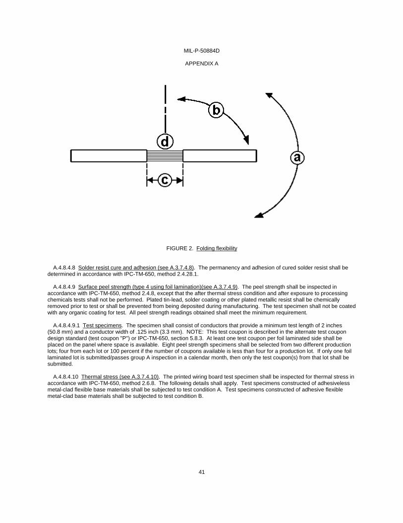
MIL-P-50884D
APPENDIX A
41
FIGURE 2. Folding flexibility
A.4.8.4.8 Solder resist cure and adhesion (see A.3.7.4.8). The permanency and adhesion of cured solder resist shall bedetermined in accordance with IPC-TM-650, method 2.4.28.1.
A.4.8.4.9 Surface peel strength (type 4 using foil lamination)(see A.3.7.4.9). The peel strength shall be inspected inaccordance with IPC-TM-650, method 2.4.8, except that the after thermal stress condition and after exposure to processingchemicals tests shall not be performed. Plated tin-lead, solder coating or other plated metallic resist shall be chemicallyremoved prior to test or shall be prevented from being deposited during manufacturing. The test specimen shall not be coatedwith any organic coating for test. All peel strength readings obtained shall meet the minimum requirement.
A.4.8.4.9.1 Test specimens. The specimen shall consist of conductors that provide a minimum test length of 2 inches(50.8 mm) and a conductor width of .125 inch (3.3 mm). NOTE: This test coupon is described in the alternate test coupondesign standard (test coupon "P") or IPC-TM-650, section 5.8.3. At least one test coupon per foil laminated side shall beplaced on the panel where space is available. Eight peel strength specimens shall be selected from two different productionlots; four from each lot or 100 percent if the number of coupons available is less than four for a production lot. If only one foillaminated lot is submitted/passes group A inspection in a calendar month, then only the test coupon(s) from that lot shall besubmitted.
A.4.8.4.10 Thermal stress (see A.3.7.4.10). The printed wiring board test specimen shall be inspected for thermal stress inaccordance with IPC-TM-650, method 2.6.8. The following details shall apply. Test specimens constructed of adhesivelessmetal-clad flexible base materials shall be subjected to test condition A. Test specimens constructed of adhesive flexiblemetal-clad base materials shall be subjected to test condition B.
MIL-P-50884D
APPENDIX A
42
A.4.8.5 Electrical inspection.
A.4.8.5.1 Continuity (see A.3.7.5.1). A current shall be passed through each net by applying electrodes on the terminals ateach end of the net. The current passed through the net shall not exceed those specified in the applicable design standard(see A.3.1.1 and appendix D) for the smallest conductor in the circuit.
A.4.8.5.2 Circuit shorts (isolation resistance)(see A.3.7.5.2). A test voltage shall be applied between each net and all othernets that are adjacent to the net under test. The voltage shall be applied between nets of each layer and the electricallyisolated net of each adjacent layer. For manual testing the voltage shall be 200 volts minimum and shall be applied for aminimum of 5 seconds. When automated test equipment is used, the minimum applied test voltage shall be as specified onthe applicable master drawing. If a test voltage of the printed wiring board is not specified on the applicable master drawing,the test voltage shall be the maximum rated voltage of the net being tested. If no maximum rated voltage is specified, theminimum test voltage shall be 40 volts.
A.4.8.5.3 Dielectric withstanding voltage (see A.3.7.5.3). The printed wiring board test specimen shall be tested inaccordance with IPC-TM-650, method 2.5.7, test condition B. The following details and exceptions apply:
a. Test specimen: The test specimen shall be as identified in tables I or IV.
b. Magnitude of test voltage: Condition B (1,000 V dc +25 V dc, -0 V dc).
c. Duration of application of test voltage: 30 seconds +3, -0 seconds.
d. Points of application: The dielectric withstanding voltage shall be applied between all common portions of eachconductor pattern and all adjacent common portions of each conductor pattern. The voltage shall be appliedbetween conductor patterns of each layer and the electrically isolated pattern of each adjacent layer.
A.4.8.6 Environmental inspection.
A.4.8.6.1 Moisture and insulation resistance (see A.3.7.6.1). The printed wiring board test specimen shall be tested inaccordance with IPC-TM-650, method 2.6.3, class 3, test specimen preparation method A. The initial and final resistancemeasurements shall be taken at 500 V dc, +25 V dc, -0 V dc).
A.4.8.6.2 Thermal shock (see A.3.7.6.2). The printed wiring board test specimen shall be tested in accordance withIPC-TM-650, method 2.6.7.2, with the following exceptions:
a. The printed wiring board test specimens shall be subjected to 100 temperature cycles in accordance with testcondition D of IPC-TM-650, method 2.6.7.2.
b. Transfer time between chambers shall be less than 2 minutes. The thermal capacity of the test chambers used shallbe such that the ambient temperature shall reach the specified temperature within 2 minutes after the specimen hasbeen transferred to the appropriate chamber.
c. During the test, a resistance measurement shall be taken during the first and last high temperature cycle.
MIL-P-50884D
APPENDIX A
43
A.5 PACKAGING
A.5.1 Packaging. For acquisition purposes, the packaging requirements shall be as specified in the contract or order (see6.2). When actual packaging of materiel is to be performed by DoD personnel, these personnel need to contact theresponsible packaging activity to ascertain requisite packaging requirements. Packaging requirements are maintained by theInventory Control Point's packaging activity within the Military Department or Defense Agency, or within the MilitaryDepartment's System Command. Packaging data retrieval is available from the managing Military Department's or DefenseAgency's automated packaging files, CD-ROM products, or by contacting the responsible packaging activity.
A.6 NOTES
(This section contains information of a general or explanatory nature that may be helpful, but is not mandatory.)
A.6.1 Intended use. This appendix is intended to be used by manufacturers not certified to the QML printed boardspecification, MIL-PRF-31032. This appendix is not a duplicate or look-alike of any MIL-PRF-31032 associated specification,most of the historic performance and verification requirements are still contained in this appendix. However, many of the"enhanced" acceptance criteria or methods developed for MIL-PRF-31032 associated specifications have been added as thebaseline or are available as an option.
A.6.2 Acquisition requirements.
A.6.2.1 Acquisition requirements. Acquisition documents must specify the following:
a. Title, number, revision letter (with any amendment number when applicable), and date of this specification.
b. Issue of DoDISS to be cited in the solicitation, and if required, the specific issue of individual documents referenced(see 2.2 and A.2.1.1).
c. Appropriate type (see 1.2.1) and base material designations (see 1.2.2).
d. Title, number, revision letter (with any engineering change proposal or notice of revision number when applicable),and date of the applicable master drawing (see 3.1.1).
e. Title, number, revision letter (with any notice number when applicable), and date of the applicable design standard(see A.3.3).
f. Part identification (if applicable), and marking instructions including size, location and application method (seeA.3.1.1 and A.3.8).
g. Whether microsectioned test specimens, samples or photographs are required to be delivered with the order.
h. Packaging requirements (see A.5.1).
MIL-P-50884D
APPENDIX A
44
A.6.2.2 Additional acquisition requirements. Acquisition documents should also specify the following data, if applicable:
a. Verification Conformance Inspection option (if other than option 4)(see appendix D).
b. Design related if different than the applicable design standard (see appendix D).
(1) Minimum annular ring (external or internal)(see A.3.1.1), if different than the applicable design standard.
(2) Minimum conductor width (see A.3.1.1), if different than the applicable design standard.
(3) Minimum conductor spacing (see A.3.1.1), if different than the applicable design standard.
(4) Minimum dielectric thickness (see A.3.1.1), if different than the applicable design standard.
(5) Minimum edge spacing requirement (see A.3.1.1), if different than the applicable design standard.
(6) Copper plating thickness (see A.3.1.1), if different than the applicable design standard.
(7) Conductor finish plating (see A.3.1.1), if other than solder coating or tin-lead.
c. Conductor edge outgrowth or overhang, if applicable (see A.3.7.4.2).
d. Circuit shorts (isolation resistance) requirements (see A.3.7.5.2).
e. Surface (foil lamination) peel strength, if applicable (see A.3.7.4.9).
f. Non-delivery of sample units which have not been subjected to electrical testing (continuity and circuit shorts tests)and have passed all other tests to groups A and B inspection.
g. Cleanliness (organic)(see A.3.7.3.1 and A.6.5).
h. If special or other identification marking is required (see A.3.8).
A.6.3 Qualification. Although the qualification test specimen master drawings IPC-100041, IPC-100042, and IPC-100043specified in A.2.1.1 requires the use of flexible materials compliant to specific slash sheets (usually /1, /2, /3, or /4) inIPC-FC-231, IPC-FC-232, IPC-FC-233 and IPC-FC-241, and rigid base materials compliant to MIL-P-13949 (nowMIL-S-13949), manufacturer's can qualify base material not addressed by IPC-FC-241 or MIL-S-13949 by specifying the basematerial on the application for qualification. In addition, the Zone C (except for test coupon E 5) of the qualification masterdrawing is required to be present on the qualification test specimen and is required for qualification testing.
A.6.3.1 Transference of qualification. Manufacturers currently qualified to MIL-P-50884C will have their qualificationtransferred to this document. The expiration date of their current qualification will not be changed. Qualifications in process(before the date of this document) will be performed to the requirements MIL-P-50884C with amendment 4. New applicationsfor qualification (after the date of this document) must be performed to the requirements of this revision.
MIL-P-50884D
APPENDIX A
45
A.6.3.2 Qualification expiration and QPL-50884. Qualification listings within QPL-50884 for manufacturers qualified underthis appendix (QPL product assurance level) includes the qualification expiration date as the last six digits of the test referencenumber. This date, formatted as (month/day/year), is the actual qualification expiration date for that listing. This date signifiesthat the company is no longer qualified (unless notified in writing by the qualifying activity) whether or not that individual listinghas been removed the QPL. If the company has not requalified before the next issue of the QPL is published, then the listingwill not be included on the QPL.
A.6.4 Terms and definitions.
A.6.4.1 Base material types. Qualification of a particular flexible base material types will be extended to cover all flexiblebase material types of that same family.
a. Adhesiveless family includes all base materials that use other techniques to hold the basis metal to one or bothsides of the dielectric.
b. Adhesive family include all base materials that rely/use an adhesive to hold the metal to both sides of the dielectric. Note "cast" materials are considered adhesiveless.
A.6.4.2 Complex (as related to group B testing). Complexity of printed wiring boards will usually depend on the basematerials used; dielectric layer thickness; overall printed wiring board thickness; number of conductor layers; conductor widthsand spacings; intricacy of patterns; size, quantity, aspect ratio and positioning of plated holes; tolerancing of any or all of theabove; the presence of internal thermal planes or heat sinks, and all combinations of the above with respect to theirmanufacturing difficulty, and their effects upon the consistent ability of the printed wiring boards to meet the requirements ofthe periodic testing, unless otherwise specified by the contracting activity.
A.6.4.3 Conductive interfaces. The term conductive interfaces is used to describe the junction between the hole wallplating or coating and the surfaces of internal and external layers of metal foil. The interface between platings and coating(electroless copper, direct metallization copper and non-electroless electroless copper substitutes, etc., and electrolyticcopper, whether panel or pattern plated), are also considered a conductive interface.
A.6.4.3.1 External conductive interfaces. An external conductive interface is considered to be the junction between thesurface copper foil and the deposited or plated copper.
A.6.4.3.2 Internal conductive interfaces. An internal conductive interface is considered to be the junction between theinternal layers (copper foil posts or internal layers) and the deposited or plated copper.
A.6.4.4 Contract service(s). Contract services are those services contracted or performed (or both) outside the qualifiedmanufacturer's immediate facility, not to include verification testing including electrical function tests.
A.6.4.4.1 Mass lamination. Manufacturers requesting to use contract services lamination (mass lamination) must bequalified to type 4 of the same base material type requested. The qualification test specimens and sample size must be asspecified in A.4.5.2.1. The qualification test specimens must be produced by the QPL manufacturer and the mass laminatorand must be representative of the subsequent production process. Printed wiring board manufacturers using contractservices are subject to the conditions of A.4.5.3.3.

MIL-P-50884D
APPENDIX A
46
A.6.4.5 Printed wiring board test specimen. The term printed wiring board test specimen is used to describe all of thefollowing; production printed wiring boards, qualification test specimens, or test coupons.
A.6.4.6 Resin systems families.
A.6.4.6.1 Thermosetting resin. For the purposes of this document, the following base material types are classified ascontaining thermosetting resins: AF, BF, BI, GB, GC, GF, GH, GI, GM, QI, and SC.
A.6.4.6.2 Thermoplastic resin. For the purposes of this document, the following base material types are classified ascontaining thermoplastic resin: GR, GP, GT, GX, and GY.
A.6.4.7 Printed board thickness. The overall printed wiring board thickness includes metallic depositions, fusing, andsolder resist. The overall thickness is measured across the printed wiring board extremities (thickest part), unless a criticalarea, such an edge card connector or card guide mounting location, is identified on the master drawing.
A.6.4.8 Quality-conformance test circuitry (QCTC). See IPC-T-50.
A.6.4.9 As received (microsection condition). As received means after tin-lead is reflowed or fused or after solder coatingbut prior to thermal stress, rework simulation, thermal shock or bond strength testing.
A.6.4.10 Fold cycle.
a. A fold cycle is defined as taking one end of the specimen and folding it around a mandrel and then unfold back tothe original starting position, traveling 180 degrees in one direction and 180 degrees in the opposite direction.
b. A fold cycle may also be defined as folding (using opposite ends) the ends toward each other (fold the samedirection) and then unfold back to the original starting position, with each end traveling 90 degrees in one directionand 90 degrees in the opposite direction.
A.6.5 Cleanliness.
A.6.5.1 Flux removal. Selection of procedures for flux removal is at the manufacturer's discretion. A procedure should bechosen which will enable the printed wiring board fabricator to produce results enabling compliance with this document. Bothpolar and nonpolar solvents may be required to effect adequate flux removal.
A.6.5.2 Alternate methods and equipment. The following methods of determining the cleanliness of printed wiringboards have been shown to be equivalent to the sodium chloride equivalent ionic contamination test method:
a. The Kenco Alloy and Chemical Company, Incorporated, "Omega Meter, Model 200."
b. Alpha Metals Incorporated, "Ionograph."
c. Zero Systems, Incorporated, "Zero Ion, Model ZI-100."
d. Westek, "ICOM 5000."
A.6.6 Certified suitable laboratories (acceptable to the Government). Government accepted test laboratories are thosefacility that have demonstrated their ability to perform the verification test required by this document. Levels of acceptanceinclude group A, group B, group C, and qualification testing.

MIL-P-50884D
APPENDIX A
47
TABLE VI. Equivalence factors.
Equivalents of sodium chloride Method Equivalence
factors Micrograms persquare inch
Micrograms persquare cm
RelatedIPC-TM-650test method
Resistivity of solvent extract 1.00 10.06 1.56 2.3.5
Omega meter 1.39 14.00 2.20 2.3.26
Ionograph 2.01 20.00 3.10 2.3.26.1
Zero ion 3.68 37.00 5.80 N/A
ICOM 5000 2.20 22.00 3.40 N/A
A.6.7 Alternate test methods. Other test methods may be substituted for those specified herein provided it is demonstratedto and approved by the qualifying activity that such a substitution in no way relaxes the requirements of this specification.
A.6.7.1 Flexibility endurance (see A.4.8.4.3). The flexibility endurance test may be performed using the alternate testprocedure detailed in IPC-TM-650, method 2.4.3.1.
A.6.8 Group B sample critical design details. Past versions of this document contained default design details that wereassumed to apply to all test coupons subjected to group B inspection, regardless of the master drawing design requirements. With the issuance of this document, the design details which were universally used to determine acceptance or failure of thegroup B samples, are no longer considered universally applicable to the group B test coupons. The printed wiring boarddesign details (plating thickness, dielectric separation, external, and internal annular ring, etc.) or the default design standardthat applies to the test coupons, should be submitted along with test coupons so that a proper group B evaluation of thedesign can be completed.
EXAMPLE: The master drawing of the most complex design selected for group B testing requires .003 inch (0.08 mm) ofcopper plating thickness, .006 inch (0.15 mm) of dielectric spacing, and .005 inch (0.13 mm) internal annular ring. Thesedesign details are considerably different than the baseline design parameters found in either IPC-2223 or IPC-2221. If onthese same samples, the group B test laboratory found that the samples exhibited .002 inch (0.05 mm) of copper platingthickness, .005 inch (0.13 mm) of dielectric spacing and .004 inch (0.10 mm) internal annular ring, the test laboratory could notclaim, state, or certify that the results of group B testing or the samples met the specification requirement.
A.6.9 Stiffener adhesion test and requirement. This document does not include the stiffener adhesion test or requirementcontained in MIL-P-50884C. All stiffeners are viewed as a mechanical support and total bonding of the stiffener to the printedwiring board is not required for compliance with this document.
A.6.10 Figures and illustrations. This document contain very few figures or illustrations depicting acceptable or rejectableconditions as in previous revisions. The diagrams, figures, and illustrations (but not the accept/reject values) contained inIPC-A-600 should be used in visualizing many of the acceptable or rejectable conditions.

MIL-P-50884D
APPENDIX B
48
OPTIONAL QPL/QML PRODUCT ASSURANCE REQUIREMENTSFOR QUALIFIED MANUFACTURER LIST PROGRAMS
B.1. SCOPE
B.1.1 Scope. This appendix contains optional requirements concerning the QPL/QML product assurance level for printedwiring boards covered by this specification. The process for extending qualification is also outlined herein. This appendix isnot a mandatory part of this specification. It can be used only by manufacturers certified or qualified for listing onQML-31032. The information contained herein is intended for guidance only.
B.2. APPLICABLE DOCUMENTS
B.2.1 General. The documents listed in this section are specified in sections 3 and 4 of this specification. This sectiondoes not include documents cited in other sections of this specification or recommended for additional information or asexamples. While every effort has been made to ensure the completeness of this list, document users are cautioned that theymust meet all specified requirements documents cited in sections 3 and 4 of this specification, whether or not they are listed.
B.2.2 Government documents.
B.2.2.1 Specifications, standards, and handbooks. The following specifications, standards, and handbooks form a part ofthis document to the extent specified herein. Unless otherwise specified, the issues of these documents are those listed in theissue of the Department of Defense Index of Specifications and Standards (DoDISS) and supplement thereto, cited in thesolicitation (see 6.2).
SPECIFICATIONS
DEPARTMENT OF DEFENSE
MIL-PRF-31032 - Printed Circuit Board/Printed Wiring Board, General Specification for.
(Unless otherwise indicated, copies of the above document are available from the Document Automation and ProductionServices, Building 4D (DPM-DODSSP), 700 Robbins Avenue, Philadelphia, PA 19111-5094.)
B.2.3 Order of precedence. In the event of a conflict between the text of this document and the references cited herein,the text of this document takes precedence. Nothing in this document, however, supersedes applicable laws andregulations unless a specific exemption has been obtained.
B.3 REQUIREMENTS
B.3.1 Performance requirements. The performance requirements of the applicable MIL-PRF-31032 associatedspecification shall apply to all printed wiring boards procured to the QPL/QML product assurance level.
B.3.2 Accept/reject criteria. The accept/reject criteria of the applicable MIL-PRF-31032 associated specification shallapply to all printed wiring boards procured to the QPL/QML product assurance level.
B.3.3 QML brand. At the option of the manufacturer, the QML brand specified in MIL-PRF-31032 may be placed onprinted wiring boards that comply with the product assurance requirements of this appendix.

MIL-P-50884D
APPENDIX B
49
B.4 VERIFICATION
B.4.1 Qualification inspection (reciprocal qualification from MIL-PRF-31032). A reciprocal qualification listing (i.e., from atechnology qualified to a MIL-PRF-31032 associated specification) to this document will depend on the level of QMLtechnology qualified. Unless otherwise detailed in MIL-PRF-31032 qualification test plan, following guidelines will apply:
a. Printed board type (see 6.4.2, A.4.5.4.1, and D.3.6). The extent of qualification for base materials types defined inA.4.5.4 will apply. EXAMPLE: A type 2 qualification under a MIL-PRF-31032 associated specification will notjustify a type 4 qualification listing to this document.
b. Printed board material (see A.4.5.4.3). The extent of qualification for base materials types defined in A.4.5.4 willapply. EXAMPLE: An adhesiveless flexible metal clad base material qualification under a MIL-PRF-31032associated specification will justify an adhesiveless flexible metal clad base material qualification listing to thisdocument.
c. Complexity. The manufacturer can only supply QPL/QML technology equal to or less than their QML capability(unlike the QPL product assurance level with its unlimited multilayer capability qualification). EXAMPLE: A type 4, 6conductor layer adhesiveless flexible base material qualification under a MIL-PRF-31032 associated specificationwill allow a type 4, adhesiveless flex with GF cap layer base material reciprocal qualification listing to this document;however, the manufacturer could certify up to 8 layers as compliant (25 percent extension of qualification as allowedby MIL-PRF-31032, rounded up). In order to supply a type 4, 10 conductor layer adhesiveless flexible base materialQPL/QML printed wiring board, the QML manufacturer would need to extend its QML qualification listing. This couldbe accomplished by using the add-on provisions of MIL-PRF-31032.
B.4.1.1 Concurrent qualification. Manufacturers already qualified to the QPL level of this document will retain that listingafter transitioning to the QPL/QML level. The 3 year expiration time will not apply to the QPL/QML product assurance level.
B.4.1.2 Retention (see B.6.4). The QML status report described in MIL-PRF-31032 will cover the QPL/QML retentionrequirements to this document.
B.4.2 QPL/QML product assurance. The product assurance requirements for the QPL/QML level of printed wiring boardfurnished under this specification shall be satisfied by certification to MIL-PRF-31032. All printed wiring boards manufacturedand delivered in compliance with this appendix should be produced in accordance with the approved quality managementplan.
MIL-P-50884D
APPENDIX B
50
B.4.3 Printed wiring board performance verification. Printed wiring board performance verification inspection shall consistof inspections on the production printed wiring boards and test coupons specified in the applicable MIL-PRF-31032 associatedspecification. The following details are applicable to the QPL/QML product assurance level:
a. Lot conformance inspection (LCI) product acceptance testing should be based on the applicable verification flows(in-process and group A) offered by this document (see A.4.4 and appendix D) or the routine from a similartechnology described by a MIL-PRF-31032 associated specification. The various verification flows should be basedupon the design standard used to design the printed wiring boards and the available panel test coupons for theprinted wiring boards.
b. MIL-PRF-31032 periodic conformance inspection (PCI) program can be used in lieu of groups B and C inspection ofthis document.
c. Test optimization is applicable to this appendix and can be applied to any verification flow detailed in this document.
B.5. PACKAGING
B.5.1 Packaging. For acquisition purposes, the packaging requirements shall be as specified in the contract or order (see6.2). When actual packaging of materiel is to be performed by DoD personnel, these personnel need to contact theresponsible packaging activity to ascertain requisite packaging requirements. Packaging requirements are maintained by theInventory Control Point's packaging activity within the Military Department or Defense Agency, or within the MilitaryDepartment's System Command. Packaging data retrieval is available from the managing Military Department's or DefenseAgency's automated packaging files, CD-ROM products, or by contacting the responsible packaging activity.
B.6 NOTES
B.6.1 Intended use. This appendix is intended to be used by manufacturers certified to MIL-PRF-31032 to reduce thecomplexity of maintaining multiple product/process and testing flows (both MIL-P-50884 or MIL-PRF-31032) within a themanufacturing and testing facility.
B.6.2 Application of the QPL/QML product assurance level to existing requirements.
B.6.2.1 Use of existing master drawings. The QPL/QML printed wiring board manufacturer can use pre-existing masterdrawing and production artwork without any modifications (existing production masters test coupons and requires noadditional or new ones).
B.6.2.2 Form, fit, and function. The form, fit, and function of the printed wiring boards, whether the QPL/QML productassurance level or the QPL product assurance level is used, will be the same.
B.6.2.3 Certification. The printed wiring boards can be certified as being compliant to this document (MIL-P-50884).

MIL-P-50884D
APPENDIX B
51
B.6.3 Benefits of the QPL/QML product assurance level. Printed wiring boards produced by QML manufacturers using theprovisions of this appendix in lieu of previous revisions would be compliant to this document (MIL-P-50884) via the QPL/QMLproduct assurance level with the added benefits as follows:
a. The QPL/QML manufacturer can use pre-existing master drawing and production artwork without any modificationsneeded (can use existing production masters test coupons and requires no additional or new ones).
b. The printed wiring boards, whether the QPL/QML option or the QPL option is used, will be the same.
c. The level of quality will be the same or higher than the QPL product assurance level.
d. When using the correct (for the design) verification test, the cost should be the same or less due to enhancementsmade to accept/reject criteria.
e. Customers will be more confident that a QPL/QML manufacturer has demonstrated the capabilities to build itsdesign dues to its QML certification and qualification rather the generic standardized qualification test vehicle of theQPL quality assurance level portion of this document.
B.6.4 Retention issues. The manufacturer need only to keep the qualifying activity apprised of it total QML program, i.e.,MIL-PRF-31032 QML and this document's QPL/QML product assurance level. This means that the manufacturer does nothave to maintain two separate compliance programs, (i.e., no need for a QPL compliance program for this document and aQML program for MIL-PRF-31032).
B.6.5 Certificates of compliance issues. The manufacturer can certify QPL/QML printed wiring boards process under theirMIL-PRF-31032 QML program as compliant to this document. The certificate of compliance should reference the QPL/QMLproduct assurance level to differentiate the compliant product from printed wiring boards verified using the QPL productassurance level offered in this document.
B.6.6 Past specification revisions (see appendix D for more details). Printed wiring boards procured to this documentmeets and/or exceeds all quality and reliability requirements of previous revisions of MIL-P-50884.

MIL-P-50884D
APPENDIX C
52
C = 0 (ZERO DEFECT) SAMPLING
C.1. SCOPE
C.1.1 Scope. This appendix details the statistical sampling procedures to be used with the QPL product assurance levelof this specification. This appendix is a mandatory part of this specification. The information contained herein is intendedfor compliance only.
C.2. APPLICABLE DOCUMENTS. This section is not applicable to this appendix.
C.3. DEFINITIONS AND SYMBOLS.
C.3.1 Definitions. The following definitions shall apply for all statistical sampling procedures:
a. C = 0 sample plan: The C = 0 sample plans are defined as a combination of a test specimen usage identifier (seeC.3.1.b below) and a sample size series (see C.3.1.c below). The resulting C = 0 sample plan will be a twocharacter designator combination that identifies the sample size series that is to be with a type of test specimen fora particular verification (see C.4.5).
b. Test specimen usage identifier (see C.4.5 for examples): The following usage modifiers are used to differentiatewhen a particular plan is to be used for a particular test specimen:
(1) The letter "B" will be used to signify that production printed boards are to be sampled.
(2) The letter "T" will be used to signify that test coupons are to be sampled.
(3) An asterisk "*" will be used for either printed boards or test coupons.
c. Sample size series: The sample size series is defined as the following series of letters: A, D, F, H, J, L, and N thatare listed in table VII (see C.4.5 for examples).
d. Tightened inspection: Tightened inspection is defined as inspection performed using the next sample size valuein the sample size series lower than that specified.
e. Acceptance number (C): The acceptance number is defined as an integral number associated with the selectedsample size which determines the maximum number of defectives permitted for that sample size.
f. Rejection number (R): Rejection number is defined as one plus the acceptance number.
C.3.2 Symbols. The following symbols shall apply for all statistical sampling procedures:
a. C: Acceptance number.
b. R: Rejection number.
MIL-P-50884D
APPENDIX C
53
C.4. STATISTICAL SAMPLING PROCEDURES AND SAMPLE PLAN TABLE
C.4.1 General. Statistical sampling shall be conducted using the C=0 method. The C=0 method as specified herein is asampling plan that provides a high degree of assurance that a lot having a proportion defective greater than the specifiedacceptance number (C=0) will not be accepted. For all situations, the acceptance number (C) shall be equal to 0 (C=0) andthe rejection number (R) shall be 1 or greater (R ≥ 1).
C.4.2 Acceptance and procedure.
C.4.2.1 Acceptance number (C = 0). Acceptance of inspection lots shall be based on an acceptance number of zero (C =0).
C.4.2.2 Rejection number (R ≥ 1). Failure of a sample unit for one or more tests of a subgroup shall be charged as a singlefailure. One or more sample rejects shall be cause for failure of the lot or sublot, as applicable. Any failure on any of thesample units shall constitute a failure of the entire inspection lot or sublot.
C.4.3 Tightened inspection (for reevaluation purposes). Tightened inspection shall be performed by sampling using doublethe sample size as specified in table VII or 100 percent with zero failures allowed.
C.4.4 Sample size. The sample size for each subgroup shall be determined from table VII. If lot size is smaller thansample size, test all of the units. The manufacturer may, at their option, select a sample size greater than that required;however, the number of failures permitted shall not exceed the acceptance number.
C.4.5 C = 0 sample plan construction (selection and usage of the sample size series). The sample size series of table VIIto be used will be directed from the appropriate inspection table. The inspection table will specify the C = 0 sample plan (testspecimen identifier and sample size series) or plans (test printed wiring board, test coupons, or either one) to use.
EXAMPLES: If an inspection table specified that "Plan BF or TL" be used when verifying test specimens, it is specifying thatsample size series "F" of table VII must be used for selecting printed wiring boards and sample size series "L" must be usedfor selecting test coupons. If the same inspection table specified that "Plan *H" be used, then sample size series "H" of tableVII can be used for either printed wiring boards or test coupons.

MIL-P-50884D
APPENDIX C
54
TABLE VII. C = 0 (zero defect) sampling.
Sample size (number of test specimens to be inspected) 1/Lot size
Series A Series D Series F Series H Series J Series L Series N
1 to 8 All All All 5 3 2 1
9 to 15 All All 13 5 3 2 1
16 to 25 All All 13 5 3 2 1
26 to 50 All 32 13 5 5 3 1
51 to 90 50 32 13 7 6 4 2
91 to 150 50 32 13 11 7 5 2
151 to 280 50 32 20 13 10 6 2
281 to 500 50 48 29 16 11 7 3
501 to 1200 75 73 34 19 15 8 4
1201 to 3200 116 73 42 23 18 9 5
1/ If lot size is smaller than sample size test all of the units.
C.5. TEST EQUIPMENT AND INSPECTION FACILITIES
C.5.1 Calibration. All tests and measurements for process control, qualification testing, lot conformance inspection orperiodic conformance inspection shall be made with capable instruments whose accuracy has been verified. Calibration ofmeasurement and test equipment and test standards that control the accuracy of inspection and test equipment and facilitiesshall be in accordance with NCSL Z540, or equivalent.
C.5.2 Inspection facilities. The inspection facility used to perform qualification testing and periodic conformance inspectionshall be approved by the qualifying activity for the performance of the tests and inspection requirements of compliant printedwiring boards.
C.5.3 Acquiring activity or manufacturer imposed tests. Acquiring activity or manufacturer imposed tests shall be inaccordance with the requirements specified in the master drawing. If any additional imposed tests detect a problem, themanufacturer shall submit all panels/printed wiring boards in the lot to those tests to eliminate rejects and shall take steps todetermine and eliminate the cause of failure.
C.5.4 Test method alternatives. Alternate test methods are allowed provided that it is demonstrated to the qualifyingactivity that such alternatives in no way relax the requirements of the test method referenced by this specification (seeappendix B).
C.5.5 Procedure in case of test equipment malfunction or operator error. When it has been established that a impropertest is due to test equipment malfunction or operator error, the inspection facility shall document the results of itsinvestigations and corrective actions, if required, and shall make this information available to the qualifying activity and theacquiring activity, as applicable.

MIL-P-50884D
APPENDIX D
55
SUPERSESSION, VERIFICATION CONFORMANCE INSPECTION OPTIONS,AND USAGE OF PAST DESIGN STANDARDS
D.1. SCOPE.
D.1.1 Scope. This appendix contains information and guidance concerning the supersession of legacy Department ofDefense documents such as MIL-P-50884 revision C and MIL-STD-2118. This appendix is not a mandatory part of thisspecification. The information contained herein is intended for guidance only.
D.2. APPLICABLE DOCUMENTS.
D.2.1 General.
D.2.1.1 Non-Government publications. The following documents form a part of this document to the extent specifiedherein. Unless otherwise specified, the issues of the documents which are DoD adopted are those listed in the issue of theDoDISS cited in the solicitation. Unless otherwise specified, the issues of documents not listed in the DoDISS are theissues of the documents cited in the solicitation (see 6.2).
INSTITUTE FOR INTERCONNECTING AND PACKAGING ELECTRONIC CIRCUITS (IPC)
J-STD-003 - Solderability Tests for Printed Boards.IPC-T-50 - Interconnecting and Packaging Electronic Circuits, Terms and Definitions.IPC-D-249 - Design Standard for Flexible Single and Double-Sided Printed Boards.IPC-D-275 - Design Standard for Rigid Printed Boards and Rigid Printed Board Assemblies.IPC-2221 - Printed Board Design, Generic Standard for.IPC-2223 - Flexible Printed Boards, Sectional, Design Standard for.
(Application for copies should be addressed to the Institute for Interconnecting and Packaging Electronic Circuits, 2215Sanders Road, Suite 200 South, Northbrook, IL 60062-6135.)
D.2.2 Order of precedence. In the event of a conflict between the text of this document and the references cited herein, thetext of this document takes precedence. Nothing in this document, however, supersedes applicable laws and regulationsunless a specific exemption has been obtained.
D.3 DEFINITIONS
D.3.1 Design standard. A document that establishes the standard practices, guidelines, and default values for the designof printed wiring boards. Within this document, the term "design standard" is used to describe those documents that containthe design, construction, material, and test coupon requirements and guidelines.
D.3.2 Legacy designs or documents. See D.4.1.
D.3.3 Supersession. The act of replacing a legacy document that no longer exists or is no longer supported with acurrently supported document.
D.3.5 Quality conformance test circuitry. See IPC-T-50.
D.3.6 Printed wiring board types. The printed board types are defined in IPC-2223.
MIL-P-50884D
APPENDIX D
56
D.4 SUPERSESSION
D.4.1 Superseded specifications. Appendix A of this document includes the essential requirements of the previous revisionand can be used to supersede the following specifications:
(1) MIL-P-50884C, dated 4 May 1984 with amendment 1, dated 19 August 1988.
(2) MIL-P-50884C, dated 4 May 1984 with amendment 2, dated 22 June 1990.
(3) MIL-P-50884C, dated 4 May 1984 with amendment 3, dated 13 December 1991.
(4) MIL-P-50884C, dated 4 May 1984 with amendment 4, dated 9 April 1993.
(5) MIL-P-50884C, dated 4 May 1984 with amendment 5, dated 27 November 1998.
D.4.1.1 Reference to superseded specifications. All the requirements of this document (MIL-P-50884D) can beinterchangeable with those of MIL-P-50884. Therefore, existing procurement documents (master drawings or OEMdocuments) referencing MIL-P-50884 need not be revised, updated or changed to make reference to MIL-P-50884 in order forthis document to be used.
D.4.1.2 Revisions. Printed wiring boards tested to this document generally would meet or exceed the performancerequirements of past revisions. However, due to various changes in acceptability and evaluation criteria, testing proceduresand test coupon sampling, an exact duplication of a previous revision cannot be claimed or made in all areas of concern. Manufacturers should not pick-and-choose or mix acceptability requirements and/or test procedures from one revision ofMIL-P-50884 to another. Compliance should be either to MIL-P-50884B, MIL-P-50884C (with a specific amendment, ifapplicable), or this document entirely, unless the manufacturer documents a direct correlation between the revisions (with anyamendments, if applicable) under consideration.
D.4.2 Superseded guidelines and standards. The following design standards have been superseded by IPC-2221 andIPC-2223 for all types and classes of printed wiring boards:
MIL-STD-2118, dated 4 May 1984.MIL-P-50884B (appendix), dated 19 January 1976.MIL-P-50884A, dated 5 June 1972.
D.4.2.1 Retooling. Printed wiring boards that were designed using superseded Department of Defense design standardsdo not require conversion to IPC-2221/IPC-2223.
D.4.2.2 Superseded types. Before MIL-P-50884C, only single and double sided printed wiring boards were covered inMIL-P-50884. The obsolete type A requirements in MIL-P-50884B (flexible printed wiring that is capable of withstanding atleast one solder operation without terminal degradation) did not carry over to MIL-P-50884C. However, the type Brequirements in MIL-P-50884B (flexible printed wiring that is capable of withstanding at least five solder and unsolderoperations without terminal area degradation, i.e., rework simulation) was carried over to and extended to all printed wiringboard designs in MIL-P-50884C.

MIL-P-50884D
APPENDIX D
57
D.4.3 Testing.
D.4.3.1 Group A testing. Group A testing should be performed to the specific revision, and amendment if applicable, calledout by the acquisition documents. For example, if printed wiring boards are produced to MIL-P-50884C with amendment 1,MIL-P-50884C with amendment 3 and MIL-P-50884D, a manufacturer would be expected to perform group A testing, for theapplicable lot, to the requirements of the revision specified. In those three different revisions (C w/amendment 1, Cw/amendment 3, and D) a requirement for an acceptability criteria or test procedure may be the same or it might besignificantly different. Retention of qualification summaries for group A should list the lots produced, grouped by revision andamendment.
D.4.3.2 Group B samples and testing. Samples to be selected for group B testing should be based on the most complexcompliant printed wiring boards produced that month. For example, if printed wiring boards are produced to MIL-P-50884C,MIL-P-50884C with amendment 4 and MIL-P-50884D during a given month, and the most complex printed wiring boardsproduced that month were in the lot ordered to MIL-P-50884C with amendment 4, then that should be the lot from which thegroup B sample should be selected. The samples should be tested in accordance with MIL-P-50884C with amendment 4. Ifduring that same month, printed wiring boards were produced to MIL-P-50884B and MIL-P-50884C (unamended), group Btests to those specific revisions would also be required in order to be compliant to those revisions, unless specifically specifiedin the contract.
D.4.3.3 Group C samples and testing. Group C testing is for manufacturers of class A and class B printed wiring boards toverify that it is still capable of meeting the flexibility class performance requirements. Samples to be selected for group Ctesting, unlike group B inspection, are not based on the most complex compliant printed wiring boards produced that month orreporting period. The group C samples can be either production printed wiring boards or the appropriate test coupon.
D.4.4 Superseded test coupons. Before MIL-P-50884C, test coupons were only used for first article inspection and notrequired for production. The production panel test coupons were introduced within MIL-P-50884C and MIL-STD-2118 werefor the supplier certification program concept. The production test coupons of MIL-P-50884C, described withinMIL-STD-2118, should be used when already incorporated onto production tooling. New designs or jobs should use the testcoupons specified in IPC-2221 and IPC-2223. Table VIII contains a cross listing of the various test coupon designations thathave been used in superseded design standards.
D.4.5. Test coupons, placement, quantity and usage. IPC-2221 contains a table that specifies for each production panelthe test coupon placement, quantity (see note below) and usage (similar to IPC-D-275 and IPC-2221). However,MIL-STD-2118 did not provide a table that specifies for each production panel the test coupon placement, quantity, andusage.
NOTE: There needs to be a sufficient number of test coupons on the production panel in order to be able to perform group Aand when necessary, group B inspection regardless of the number of test coupons specified by the design standard.
D.4.5.1 Intended use and intent of this appendix. This appendix can be used to understand the test coupons that werereferenced in previous revisions of this document. These guidelines are intended for the re-identification and proper usage oftest coupons within this document that are or were originally identified in various legacy Department of Defense printed wiringboard design standards. This appendix is intended for use in conjunction with a manufacturer's verification conformancecompliancy program.
D.4.5.2 Supporting documents. The documents in this section may be used as guidelines for the development of averification conformance optimization program and are not mandatory for this specification.
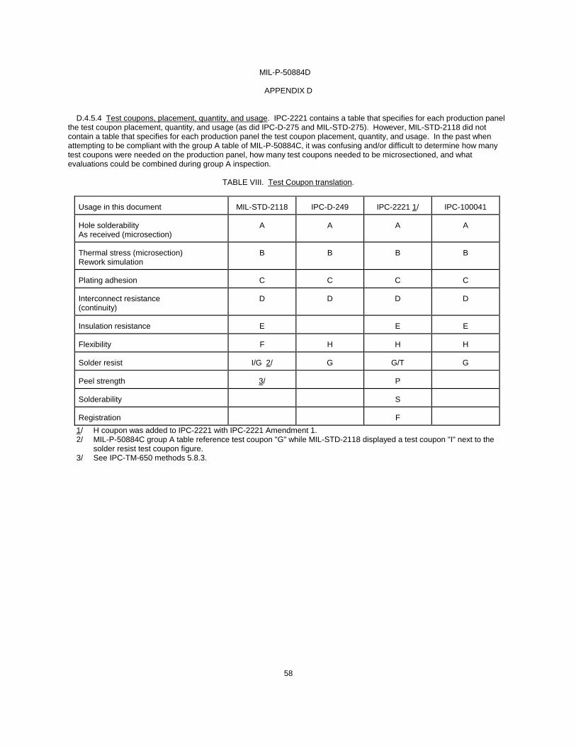
MIL-P-50884D
APPENDIX D
58
D.4.5.4 Test coupons, placement, quantity, and usage. IPC-2221 contains a table that specifies for each production panelthe test coupon placement, quantity, and usage (as did IPC-D-275 and MIL-STD-275). However, MIL-STD-2118 did notcontain a table that specifies for each production panel the test coupon placement, quantity, and usage. In the past whenattempting to be compliant with the group A table of MIL-P-50884C, it was confusing and/or difficult to determine how manytest coupons were needed on the production panel, how many test coupons needed to be microsectioned, and whatevaluations could be combined during group A inspection.
TABLE VIII. Test Coupon translation.
Usage in this document MIL-STD-2118 IPC-D-249 IPC-2221 1/ IPC-100041
Hole solderabilityAs received (microsection)
A A A A
Thermal stress (microsection)Rework simulation
B B B B
Plating adhesion C C C C
Interconnect resistance(continuity)
D D D D
Insulation resistance E E E
Flexibility F H H H
Solder resist I/G 2/ G G/T G
Peel strength 3/ P
Solderability S
Registration F
1/ H coupon was added to IPC-2221 with IPC-2221 Amendment 1.2/ MIL-P-50884C group A table reference test coupon "G" while MIL-STD-2118 displayed a test coupon "I" next to the
solder resist test coupon figure.3/ See IPC-TM-650 methods 5.8.3.

MIL-P-50884D
APPENDIX E
59
SEQUENTIAL ELECTROCHEMICAL REDUCTION ANALYSIS (SERA)SOLDERABILITY TEST
E.1. SCOPE.
E.1.1 Scope. This test method describes the method and procedure used to evaluate oxidation levels on solderablesurfaces. The type and quantity of oxides on copper, tin, and lead surfaces have a significant impact on solderability. Theprocedure involves using electrochemical reduction techniques to determine the type and quantity of oxide on plated-through holes, attachment lands, and printed wiring board surface conductors. The SERA solderability test method isoffered as an alternative to other solderability test methods required by this document. This test method shall not becontractually imposed upon either the contractor or sub-contractor. This appendix is not a mandatory part of thespecification. The information contained herein is intended for compliance only when volunteered as an alternative to theother solderability test methods detailed.
E.2. APPLICABLE DOCUMENTS.
E.2.1 General. The documents listed in this section are specified in sections 3 and 4 of this specification. This sectiondoes not include documents cited in other sections of this specification or recommended for additional information or asexamples. While every effort has been made to ensure the completeness of this list, document users are cautioned that theymust meet all specified requirements documents cited in sections 3 and 4 of this specification, whether or not they are listed.
E.2.2 Government documents.
E.2.2.1 Specifications, standards, and handbooks. The following specifications, standards, and handbooks form a part ofthis document to the extent specified herein. Unless otherwise specified, the issues of these documents are those listed in theissue of the Department of Defense Index of Specifications and Standards (DoDISS) and supplement thereto, cited in thesolicitation (see 6.2).
SPECIFICATIONS
FEDERAL
A-A-59282 - Chemicals, Analytical; General Specification for.
(Unless otherwise indicated, copies of federal specifications are available from the Document Automation and ProductionServices (DAPS), Building 4D (DPM-DODSSP), 700 Robbins Avenue, Philadelphia, PA 19111-5094.)
E.2.2 Non-Government publications. The following documents form a part of this document to the extent specifiedherein. Unless otherwise specified, the issues of the documents which are DoD adopted are those listed in the issue of theDoDISS cited in the solicitation. Unless otherwise specified, the issues of documents not listed in the DoDISS are theissues of the documents cited in the solicitation (see 6.2).
ASSOCIATION CONNECTING ELECTRONICS INDUSTRIES (IPC)
J-STD-004 - Soldering Fluxes, Requirements for.
(Application for copies should be addressed to the Institute for Interconnecting and Packaging Electronic Circuits, 2215Sanders Road, Suite 200 South, Northbrook, IL 60062-6135.)
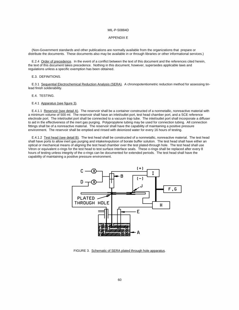
MIL-P-50884D
APPENDIX E
60
(Non-Government standards and other publications are normally available from the organizations that prepare ordistribute the documents. These documents also may be available in or through libraries or other informational services.)
E.2.4 Order of precedence. In the event of a conflict between the text of this document and the references cited herein,the text of this document takes precedence. Nothing in this document, however, supersedes applicable laws andregulations unless a specific exemption has been obtained.
E.3. DEFINITIONS.
E.3.1 Sequential Electrochemical Reduction Analysis (SERA). A chronopotentiometric reduction method for assessing tin-lead finish solderability.
E.4. TESTING.
E.4.1 Apparatus (see figure 3).
E.4.1.1 Reservoir (see detail A). The reservoir shall be a container constructed of a nonmetallic, nonreactive material witha minimum volume of 500 ml. The reservoir shall have an inlet/outlet port, test head chamber port, and a SCE referenceelectrode port. The inlet/outlet port shall be connected to a vacuum trap tube. The inlet/outlet port shall incorporate a diffuserto aid in the effectiveness of the inert gas purging. Polypropylene tubing may be used for connection tubing. All connectionfittings shall be of a nonreactive material. The reservoir shall have the capability of maintaining a positive pressureenvironment. The reservoir shall be emptied and rinsed with deionized water for every 16 hours of testing.
E.4.1.2 Test head (see detail B). The test head shall be constructed of a nonmetallic, nonreactive material. The test headshall have ports to allow inert gas purging and intake/expulsion of borate buffer solution. The test head shall have either anoptical or mechanical means of aligning the test head chamber over the test plated-through hole. The test head shall useVitron or equivalent o-rings for the test head to test surface interface seals. These o-rings shall be replaced after every 8hours of testing unless integrity of the o-rings can be documented for extended periods. The test head shall have thecapability of maintaining a positive pressure environment.
FIGURE 3. Schematic of SERA plated through hole apparatus.

MIL-P-50884D
APPENDIX E
61
E.4.1.3 Vacuum pump (see detail C). A vacuum pump shall be used to draw buffer solution into and out of the test headcompartment. The vacuum pump shall be able to draw minimum vacuum of 5 inches of Hg (15 kPa).
E.4.1.4 Gas regulator (see detail D). An in-line gas regulator shall be used to monitor the flow of the inert purging gas. The gas regulator shall be able to measure a minimum of 1 cubic foot per hour (0.02832 cubic meters per hour) at standardtemperature and pressure.
E.4.1.5 SCE reference electrode (see detail E). The reference electrode shall be a saturated calomel electrode (SCE) witha temperature range of -5°C to +60°C and a Ph range of 0-14. The SCE reference electrode shall be stored in such a manneras to prevent drying out (either in a saturated KCI solution or in accordance with the manufacturer's instructions). The SCEreference electrode shall be calibrated in accordance with the manufacturer's instructions once every 30 days.
E.4.1.6 Computer (see detail F). The computer shall be equivalent to or better than a MS-DOS compatible, 80286-12MHz,with 512 Kbyte of internal memory and floppy and hard disk drives.
E.4.1.7 IEEE-488 interface card (see detail G). An IEEE-488 interface card is required for data acquisition between thecomputer, the digital multimeter, and the programmable current source.
E.4.1.8 Digital multimeter (see detail H). A digital multimeter is required to measure the voltage changes during the SERAreduction. The digital multimeter shall have the following characteristics:
a. A measurable voltage range of 0 V to -2.0 V.
b. A voltage measurement tolerance of ±5 mV.
c. Voltage measurement RMS noise level should not exceed 10 Mv.
d. Input impedance should be greater than 1 G-Ohm.
E.4.1.9 Programmable current source (see detail I). A programmable current source is required to apply a constant currentduring the SERA reduction. The programmable current source shall have the following minimum characteristics:
a. The applied current should be variable in 0.1 • amp steps between 1.0 • amps and 10 • amps.
b. The applied current should remain constant within ±5 percent.
E.4.1.10 Printed wiring board (PWB) contact pin (see detail J). A contact pin is required to complete the electrical circuitwith the test plated-through hole. The contact pin shall not exert a force of greater than .5 pounds (0.23 Kg) nor alter theplated-through hole form, fit, or function.
E.4.2 Materials.
E.4.2.1 Borate buffer solution. The SERA test requires the use of a borate buffer solution. This solution uses reagentgrade boric acid, sodium borate (Na2B407 * 10 H20), and deionized water. The recipe is 6.18 grams/liter boric acid and 9.55grams/liter of sodium borate. The Ph of the borate buffer solution shall range in the range of 8.3 - 8.4. Adjustments to thebuffer Ph shall be made using either boric acid or sodium borate additions.
E.4.2.2 Inert gas. An inert gas is required to purge oxygen from the system. Either argon or ultra high purity (99.998%) drynitrogen shall be used.

MIL-P-50884D
APPENDIX E
62
E.4.2.3 Deionized water. Deionized water comprises a portion of the borate buffer solution and shall be used to rinse thetest plated-through hole after completion of the SERA analysis. The deionized water shall be 1 Megohm conductivity orbetter.
E.4.2.4 Isopropyl alcohol. Isopropyl alcohol is used to rinse the test plated-through hole after the competition of the SERAanalysis. Reagent grade isopropyl alcohol, in accordance with A-A-59282, shall be used.
E.4.2.5 Potassium chloride solution (KCI). The SCE reference electrode may be stored in a saturated KCI solution. Thissolution uses reagent grade potassium chloride, in accordance with A-A-59282, in a saturated solution form.
E.5. PROCEDURES.
E.5.1 General. The test procedure shall be performed on three plated-through holes randomly chosen on the printed wiringboard or representative test coupon. The SERA test shall be performed just prior to packaging for storage or shipment orimmediately upon removal from the manufacturer's protective package. During handling, care shall be exercised to preventthe surfaces being tested from being abraded or contaminated by grease, perspirants, abnormal atmosphere, etc. The testprocedure consists of the following operations:
a. Proper preparation of SERA system (see E.5.2).
b. Application of test method (see E.5.3).
c. Evaluation of test data (see E.5.4).
d. Proper post test preparation of SERA system (see E.5.5).
E.5.2 Preparation of SERA systems.
a. Initiate inert gas flow into system and allow a minimum of 10 minutes to elapse prior to testing.
b. Turn on digital multimeter and programmable current source and allow a minimum of 10 minutes to elapse prior totesting.
c. Remove reference electrode port and rinse with deionized water. Replace reference electrode port and addsufficient quantity of borate buffer solution to immerse the SCE reference electrode a minimum of 1 inch (25.4 mm).
d. Remove SCE reference electrode from storage container. Rinse with deionized water, wipe with clean soft cloth,and place into reference electrode port. Attach system electrical connections in accordance with figure 3.
e. Remove and replace test head o-ring seals as required (see E.4.1.2).
f. Close SERA test head together thus seating o-rings together on a representative sample plated-through hole andperform vacuum check on system. No visible air bubbles shall be detected in the test head chamber which wouldindicate improper sealing.

MIL-P-50884D
APPENDIX E
63
E.5.3 Application of test method.
a. The test operator shall record the specimen lot date code and manufacturer for each individual printed wiring board. An individual printed wiring board reference chart for the test plated-through holes and PWB contact pin locationsshall be maintained for each test specimen configuration.
b. Insert test specimen onto SERA test head and allow a minimum of 4 seconds for inert gas purging of the test head. Ensure inert gas bubbling is occurring in the reservoir tube.
c. Attach PWB contact pin.
d. Attach electrical source leads.
e. Draw borate buffer solution into test head chamber a minimum of 75 percent of chamber height. Visually monitortest head chamber for leaks.
f. Partially flush test head chamber to 50 percent height to dislodge any gas bubbles which could be trapped in testhole.
g. Input computer data for test specimen and test hole identification. Set current density at 30 • amp per centimetersquared (plated-through hole area shall be calculated as specified in E.5.3.1), test duration at a minimum of 400seconds, the number of open circuit samples to be measured, and the number of systems measurements at onereading per second. The minimum test duration may be reduced provided complete plated-through hole reductionhas been achieved.
h. Perform SERA test to test duration completion.
i. Remove electrical source leads.
j. Remove PWB contact clamp.
k. Flush borate buffer solution from test hole.
l. Remove test specimen from SERA test head.
m. Rinse test plated-through hole with deionized water saturated cotton swab for a minimum of 3 seconds, then rinsetest plated-through hole with isopropyl alcohol saturated cotton swab for a minimum of 3 seconds. Allow test plated-through hole to air dry. The rinsing operations may be conducted for all test holes as a one time operation providedthe rinsing operation is completed within 10 minutes of completion of the last test hole on that individual printedwiring board specimen. Other documented rinsing operations may be used provided their effectiveness is as goodas or better than the cotton swab rinse process.
E.5.3.1 Plated-through hole area calculation. The area of plated-through holes shall be determined using:
Area = (2)(• )(R1)(H) + [(2)(• )(R22) - (2)(• )(R12)]
where
H = Printed wiring specimen thickness.R1 = Plated-through hole radius.R2 = O-ring internal radius.
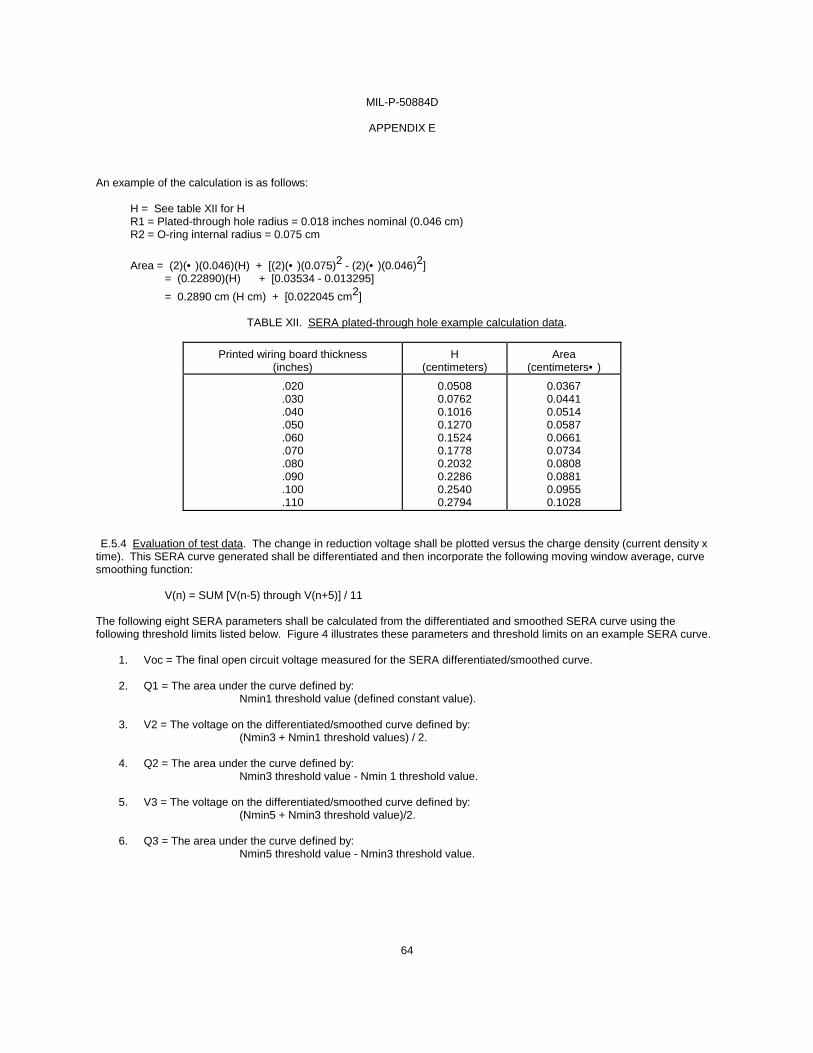
MIL-P-50884D
APPENDIX E
64
An example of the calculation is as follows:
H = See table XII for HR1 = Plated-through hole radius = 0.018 inches nominal (0.046 cm)R2 = O-ring internal radius = 0.075 cm
Area = (2)(• )(0.046)(H) + [(2)(• )(0.075)2 - (2)(• )(0.046)2]= (0.22890)(H) + [0.03534 - 0.013295]
= 0.2890 cm (H cm) + [0.022045 cm2]
TABLE XII. SERA plated-through hole example calculation data.
Printed wiring board thickness(inches)
H(centimeters)
Area(centimeters• )
.020
.030
.040
.050
.060
.070
.080
.090
.100
.110
0.05080.07620.10160.12700.15240.17780.20320.22860.25400.2794
0.03670.04410.05140.05870.06610.07340.08080.08810.09550.1028
E.5.4 Evaluation of test data. The change in reduction voltage shall be plotted versus the charge density (current density xtime). This SERA curve generated shall be differentiated and then incorporate the following moving window average, curvesmoothing function:
V(n) = SUM [V(n-5) through V(n+5)] / 11
The following eight SERA parameters shall be calculated from the differentiated and smoothed SERA curve using thefollowing threshold limits listed below. Figure 4 illustrates these parameters and threshold limits on an example SERA curve.
1. Voc = The final open circuit voltage measured for the SERA differentiated/smoothed curve.
2. Q1 = The area under the curve defined by:Nmin1 threshold value (defined constant value).
3. V2 = The voltage on the differentiated/smoothed curve defined by:(Nmin3 + Nmin1 threshold values) / 2.
4. Q2 = The area under the curve defined by:Nmin3 threshold value - Nmin 1 threshold value.
5. V3 = The voltage on the differentiated/smoothed curve defined by:(Nmin5 + Nmin3 threshold value)/2.
6. Q3 = The area under the curve defined by:Nmin5 threshold value - Nmin3 threshold value.
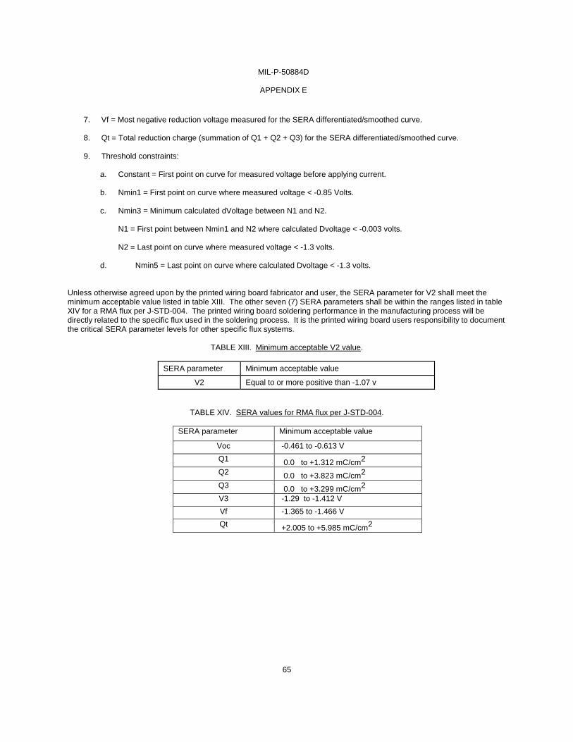
MIL-P-50884D
APPENDIX E
65
7. Vf = Most negative reduction voltage measured for the SERA differentiated/smoothed curve.
8. Qt = Total reduction charge (summation of Q1 + Q2 + Q3) for the SERA differentiated/smoothed curve.
9. Threshold constraints:
a. Constant = First point on curve for measured voltage before applying current.
b. Nmin1 = First point on curve where measured voltage < -0.85 Volts.
c. Nmin3 = Minimum calculated dVoltage between N1 and N2.
N1 = First point between Nmin1 and N2 where calculated Dvoltage < -0.003 volts.
N2 = Last point on curve where measured voltage < -1.3 volts.
d. Nmin5 = Last point on curve where calculated Dvoltage < -1.3 volts.
Unless otherwise agreed upon by the printed wiring board fabricator and user, the SERA parameter for V2 shall meet theminimum acceptable value listed in table XIII. The other seven (7) SERA parameters shall be within the ranges listed in tableXIV for a RMA flux per J-STD-004. The printed wiring board soldering performance in the manufacturing process will bedirectly related to the specific flux used in the soldering process. It is the printed wiring board users responsibility to documentthe critical SERA parameter levels for other specific flux systems.
TABLE XIII. Minimum acceptable V2 value.
SERA parameter Minimum acceptable value
V2 Equal to or more positive than -1.07 v
TABLE XIV. SERA values for RMA flux per J-STD-004.
SERA parameter Minimum acceptable value
Voc -0.461 to -0.613 V
Q1 0.0 to +1.312 mC/cm2
Q2 0.0 to +3.823 mC/cm2
Q3 0.0 to +3.299 mC/cm2
V3 -1.29 to -1.412 V
Vf -1.365 to -1.466 V
Qt +2.005 to +5.985 mC/cm2

MIL-P-50884D
APPENDIX E
66
E.5.5 Proper post test preparation of SERA system.
a. Shut off inert gas flow into system.
b. Shut off digital multimeter and programmable current source.
c. Remove SCE reference electrode, rinse with deionized water and wipe clean with clean soft cloth. Place SCEreference electrode in storage container.
d. Remove reference electrode port and dump out borate buffer solution. Rinse inner and outer surfaces of referenceelectrode port with deionized water. Replace reference electrode port into system.
e. Remove o-rings and dispose of as required (see E.4.1.2). Rinse test head o-ring seal with deionized water and wipedry with clean soft cloth.
f. Empty reservoir of borate buffer solution, rinse with deionized water, and refill with buffer solution as required (seeE.4.1.1).
E.6. NOTES
E.6.1 The equipment described herein is a result of a United States Army MANTECH Program investment. SERA is ascientific means of measuring solderability of circuit boards and components. The technology is based upon measurementsof the type and quantity of oxides using Sequential Electrochemical Reduction Analysis. Rockwell International at ThousandOaks, CA is the patent holder, and the United States Army MANTECH Program was successful in developing, proving,commercializing, and standardizing the equipment and processes. Round robin tests by a government-industry team weresuccessfully completed in the standardization effort. The United States Army has a perpetual royalty free license, and theequipment is currently on a number of weapons production lines. The technical point of contact for future inquiries should bedirected to the sole source supplier:
ECI Technology1 Madison StreetEast Rutherford, NJ 07073

MIL-P-50884D
APPENDIX E
67
FIGURE 4. Example SERA differentiated/smoothed curve.
MIL-P-50884D
68
Custodians: Preparing activity:Army - CR DLA - CCNavy - ECAir Force - 11 (Project 5998-0099)
Review activities:Army - AR, MINavy - AS, CG, MC, OS, SH, TDAir Force - 16, 99

STANDARDIZATION DOCUMENT IMPROVEMENT PROPOSAL
INSTRUCTIONS
1. The preparing activity must complete blocks 1, 2, 3, and 8. In block 1, both the document number and revision letter should be given.
2. The submitter of this form must complete blocks 4, 5, 6, and 7.
3. The preparing activity must provide a reply within 30 days from receipt of the form.
NOTE: This form may not be used to request copies of documents, nor to request waivers, or clarification of requirements oncurrent contracts. Comments submitted on this form do not constitute or imply authorization to waive any portion of the referenceddocument(s) or to amend contractual requirements.
I RECOMMEND A CHANGE:1. DOCUMENT NUMBER MIL-P-50884D
2. DOCUMENT DATE 28 December 2000
3. DOCUMENT TITLEPRINTED WIRING BOARD, FLEXIBLE OR RIGID-FLEX, GENERAL SPECIFICATION FOR
4. NATURE OF CHANGE (Identify paragraph number and include proposed rewrite, if possible. Attach extra sheets as needed.)
5. REASON FOR RECOMMENDATION
6. SUBMITTER
a. NAME (Last, First, Middle initial) b. ORGANIZATION
c. ADDRESS (Include Zip Code) d. TELEPHONE (Include Area Code)COMMERCIALDSNFAXEMAIL
7. DATE SUBMITTED
8. PREPARING ACTIVITY
a. Point of ContactDavid Corbett
b. TELEPHONECommercial DSN FAX 614-692-0526 850-0526 614-692-6939
c. ADDRESSDefense Supply Center ColumbusATTN: DSCC-VACP.O. Box 3990Columbus, OH 43216-5000
IF YOU DO NOT RECEIVE A REPLY WITHIN 45 DAYS, CONTACT:Defense Standardization Program Office (DLSC-LM)8725 John J. Kingman, Suite 2533Fort Belvoir, VA 22060-6221Telephone (703) 767-6888 DSN 427-6888
DD Form 1426, Feb 1999 (EG) Previous editions are obsolete WHS/DIOR, Feb 99