Embed Size (px)
Citation preview

The annual news magazine of the Microsystems Technology Laboratories FALL 2010
microsystems technology laboratories

CONTENTS
mtl micronotes volume four • fall 2010
http://www-mtl.mit.edu/micronotes
editor-in-chief Anantha Chandrakasanassociate editors Samuel C. Crooks
Hae-Seung “Harry” Leetechnical liason Ted Equi
art director Mara Karapetianphotography Paul McGrath
Tony RinaldoGary Riggott
© 2010 Massachusetts Institute of Technology. All rights reserved.
PSB 10-06-0276
1 NOTES FROM THE DIRECTOR
NEWS & EVENTS
2 MTL’S NEW FACULTY Introducing Li-Shiuan Peh & Dana Weinstein.
3 FOXCONN JOINS MIG
4 APPLIED MATERIALS Interactions with MTL in & out of the Fab.
5 BORN IN THE WRONG PLACE Andrea Cuomo of STMicroelectronics shares his company’s unique history.
6 TSMC DAY AT MIT
7 MTL DAY AT FOXCONN
8 MTL DAY AT TEXAS INSTRUMENTS MTL teams with the DSP Leadership University Program.
9 SAMSUNG DAY AT MTL; DR. CHANG-GYU HWANG
10 MIT & MASDAR INSTITUTE MIT & Masdar Institute develop microsystems education & research in the Middle East.
12 MARC2010
13 ENERGY RESEARCHERS FIND OBAMA AN EAGER STUDENT President showed keen interest, quick understanding and warm appreciation, say his hosts.
14 IN THE NEWS
40 GRADUATION
FEATURE STORIES
24 COLLABORATION AT ITS BEST Everyone wins when MTL and industry join forces.
30 MEDICAL ELECTRONIC SYSTEMS Can Boston become the “Silicon Valley of Medical Electronic Systems?” MTL researchers are working hard to make it happen.
34 WOMEN IN ENGINEERING MIT’s Women’s Technology Program.
RESEARCH
16 MECHANICAL DEVICES STAMPED ON PLASTIC Microelectromechanical devices gave us the Wii and the digital movie projector. MIT researchers have found a new way to make them.
18 STRAINING FORWARD Nanowires made of ‘strained silicon’— silicon whose atoms have been pried slightly apart — show how to keep increases in computer power coming.
20 TWO CHIPS IN ONE MIT team finds a way to combine materials for semiconductor manufacturing. The advance helps address the limitations of conventional silicon microprocessors.
21 SELLING CHIP MAKERS ON OPTICAL COMPUTING MTL researchers show that computing with light isn’t so far fetched.
22 LIFE AFTER SILICON Researchers in MTL are making the case for the use of exotic materials to help microchips keep improving.
23 SELF-POWERED SENSORS Harvesting electricity from small temperature differences could enable a new generation of electronic devices that don’t need batteries.
ALUMNI
36 ALUMNI UPDATE
ON THE COVER Detail of President Barack Obama’s
signature on a vacuum pump located in
the Bulovic lab.
Photo courtesy, Bulovic lab.
COLLABORATION AT ITS BEST page 24
MEDICAL ELECTRONIC SYSTEMSpage 30
WOMEN IN ENGINEERINGpage 34

1
INTRODUCTION
Welcome to the 2010 edition of the Microsystems Technology Laboratories (MTL) magazine, MTL Micronotes. MTL enjoyed another excellent year with several new multi-investigator research programs, major awards, and two
new MIG members. This past year, 35 core faculty engaged in many exciting research initiatives, including areas related to electronic device fabrication, integrated circuits and systems, photonics, MEMS, and molecular and nanotechnologies. More than 700 students and technical staff conducted research at MTL and 109 affiliate faculty members benefited directly from MTL’s fabrication and/or CAD infrastructure.
MTL hosted several technical events and seminars this year. We had two exciting distinguished seminars. Andrea Cuomo, Executive Vice President and General Manager of STMicroelectronics gave a talk titled “Born in the Wrong Place: Semiconductors Seen from Italy & France.” Chang-Gyu Hwang former CTO and President of Samsung Electronics gave a talk titled, “Ready for the Future?" We had excellent participation from the MTL community in both events. MTL’s Annual Research Conference (MARC2010) was held at the Cambridge Marriott; over 200 attendees participated. MARC offers a unique opportunity to learn about research in MTL’s diverse areas, and it encourages interaction within MTL. The students greatly appreciate the technical interactions with attendees from the MIG companies. Special thanks to Prof. Joel Voldman, Steering Committee Chair, and all the volunteers for organizing a successful event. MTL also hosted a two-day workshop on “Next-Generation Medical Electronics.” Prof. Charles Sodini continues to develop a strong medical system effort in MTL. Our MTL Seminar Series, organized by the MTL Seminar Committee and chaired by Prof. Tomas Palacios, featured a diverse set of technical presentations.
The MTL community greatly benefits from the generous financial support of the MIG, which provides subsidies for fabrication and circuit research. In addition, MIG members donate equipment, contribute directed fellowships and provide fabrication access to state-of-the-art technologies. I would like to welcome Foxconn and Hitachi High-Technologies Corporation to the MIG. We look forward to active collaborations with the new MIG companies.
Our Industrial Advisory Board (www-mtl.mit.edu/mig/iab.html) provides significant assistance in shaping MTL’s vision. We continued our successful MTL Days at MIG companies, visiting Texas Instruments and Foxconn while holding the TSMC and Samsung Days on the MIT campus. Students benefit greatly from the opportunsity to give detailed presentations to industry experts. These visits result in increased collaborations between MTL and the MIG companies.
We enjoy hearing from alumni. Please contact me with suggestions to improve MTL. I am eager to hear from you.
Sincerely, Anantha P. Chandrakasan Director, MTL

2
NEW FACULTY
Li-Shiuan Peh, Associate Professor of Electrical Engineering and Computer Science, has been at MIT since 2009. Pri-or to serving on the faculty of Princeton University, she graduated with a Ph.D. in Computer Science from Stanford Uni-versity in 2001, and a B.S. in Computer Science from the National University of Singapore in 1995. Her research focuses on low-power interconnection networks, on-chip networks and parallel computer architectures. She was awarded the CRA Anita Borg Early Career Award in 2007,
Sloan Research Fellowship in 2006, and the NSF CAREER award in 2003. Peh coins her research thrust as “network-driven computing,” where the architec-ture of future computer chips is more significantly driven by how the compute cores are interconnected, rather than the design of the cores themselves. Her re-search has motivated, proposed and pro-totyped these on-chip networks, so as to enable the continued scaling of Moore's Law into future many-core chips.
“I am excited to be jointly in CSAIL and MTL . With my research sitting right on the interface of hardware and software, it is the perfect arrangement because MTL is at the forefront of electronics –interactions with faculty and students here have been truly thrilling. MTL's interactions with industry have enabled new dimensions in my research.” —LI-SHIUAN PEH
LI-SHIUAN PEH
"MTL is home to experts in a range of research fields from whom I learn something new every day."—DANA WEINSTEIN
MTL'S NEW FACULTYIntroducing Li-Shiuan Peh and Dana Weinstein
DANA WEINSTEINProfessor Dana Weinstein and her
research group at MIT are working to
develop innovative technologies for
more-than-Moore devices. Their focus
is on developing NEMS-enhanced
electron devices to achieve high-Q, small
footprint resonators at previously inac-
cessible frequencies with the capacity
for direct integration in standard CMOS
processes. The Hybrid Devices Lab has
demonstrated acoustic resonance in
Silicon-based Independent Gate FinFETs
at multi-GHz frequencies with frequen-
cy-quality factor products rivaling those
of Quartz. Investigation of fundamental
limits of this technology and exploration
into device optimization, integration,
and control will provide circuit design-
ers with basic building blocks for RF
and mm-wave applications, including
wireless communication, high-accuracy
frequency sources for timing applica-
tions and navigation, and integrated
temperature sensing in CMOS.

3
INDUSTRIAL RELATIONS
The Microsystems Technology Laboratories (MTL) at the Massachusetts Institute of Technology and Hon Hai Precision Ind. Co. Ltd. (the anchor company of Foxconn Technology Group, Tucheng City, Taiwan, thereafter col-lectively called Foxconn) have recently announced that Foxconn has joined the Microsystems Industrial Group (MIG), an exclusive member industry consortium.
The MIG was founded in the early 1980s to support MTL infrastructure and provide direction to the labs' re-search and educational objectives in consultation with faculty leadership. The MIG also provides company mem-bers with opportunities to engage closely with faculty and students, early access to technology being developed at the lab and the ability to participate in research initiatives.
Founded in 1974 by Terry Gou, Hon Hai began as a manu-facturer of TV tuners. They are now a multinational business with group revenue exceeding $70 billion US dollars (2009). Foxconn is the largest manufacturer of 3C (Computing, Com-munication and Consumer electronics) products in the world, mainly manufacturing by contract with other companies. Foxconn’s interest in nanotechnology, heat transfer, wireless connectivity, material sciences, flat panel technology, preci-sion mold and machining, server and motherboard, opto-electronics and optical, automobile electronics, robot and automation and green manufacturing make it an ideal partner for MTL. Foxconn is the very first Microsystems Industrial Group (MIG) member working on systems-level products. MTL Director Prof. Anantha Chandrakasan sees great op-portunities in the near future for Foxconn to fit in perfectly between MTL research prototypes and real world products.
For more about MTL and Foxconn, turn to page 7.
FOXCONN JOINS MTL'S MICROSYTEMS INDUSTRIAL GROUPOpportunities for cross-collaboration and innovation abound
Green manufacturing is one of the many interests held by the Foxconn Technology Group (image, istockphoto.com)

4
INDUSTRIAL RELATIONS
APPLIED MATERIALSInteractions with MTL in and out of the Fab
Hans StorkMTL Seminar Series Lecture
On March 9th, 2010, Hans Stork, CTO, Applied Materials, provided an MTL Seminar Series lecture entitled, “Process Technologies to Enable the Path to 10nm.” In recent years, the end of Moore’s Law has become a frequent topic of debate. Maintaining the relentless pace of cost reduction is increasingly expensive, but manufacturing costs per new prod-uct continue to provide a competitive advantage. Fortunately, physics, chemistry and material science together provide engineering solutions for device and interconnect integration schemes. Mechanical and software engineering skills continue to improve productivity and control. Stork reviewed some of the exciting process capabilities that could enable several more generations of scaling down to the 10nm regime.
BIOGRAPHY Dr. Hans Stork is group vice president and chief technology officer for the Silicon Systems Group at Applied Ma-terials, Inc., where he is respon-sible for leading the company’s roadmap for silicon technology equipment. In this role, Dr. Stork oversees integrated technology
development across the silicon products, coordi-nates the organization’s industry and university engagements, and ensures value to customers by leveraging understanding of technology interactions to optimize differentiated product solutions. Prior to joining Applied Materials in October 2007, Dr. Stork served as CTO and senior vice president of Silicon Technology Development for Texas Instruments from 2001 to 2007 and as lab director for ULSI and Stor-age & Systems Labs for Hewlett Packard from 1994 to 2001. He started his professional career at IBM, where he received two outstanding achievement awards for work on Silicon-Germanium heterojunc-tion bipolar transistors (SiGe HBTs).
LEFT Mark Pinto. (Photo courtesy of Ap-plied Materials)
In November of 2008, Mark Pinto, CTO and General Man-ager of the Energy and Environmental Solutions business at Applied Materials, gave an MTL seminar titled “Has The Sun Finally Risen on Photovoltaics?” Dr. Pinto described “how photovoltaics are on the verge of becoming a major source of electrical power through a principle similar to that which underlies VLSI —the reduction of unit cost through nanomanufacturing.” This is an exciting area that resonates well with the growing MTL focus on energy-related technology.
Besides such seminars, Applied and MTL have interacted through a variety of mechanisms over the years, includ-ing visits by MTL faculty to the Applied Materials site in Santa Clara, CA. In addition, Applied has made a number of equipment donations that are a critical part of the MTL fabrication facility, including 5 Applied Materials tools: a Precision 5000 etcher, Centura 5300 oxide etcher, Endura metal sputterer, Centura 5200 Thick Dielectric CVD and Si/SiGe Epi Centura.
Applied and MTL continue to explore mechanisms for interaction that enhance research in the areas of advanced materials and processes, such as graphene, and materials and processes for solar energy and solid state lighting, in addition to the core silicon technology that has been the mainstay of Applied’s business for many years.

5
INDUSTRIAL RELATIONS
On April 26th, 2010, Andrea Cuomo, Executive Vice Presi-
dent and General Manager of Sales and Marketing for
Europe, Middle East and Africa at STMicroelectronics,
provided an MTL Distinguished Lecture entitled, “Born in the
Wrong Place: Semiconductors Seen from Italy & France.”
Andrea Cuomo’s talk provided a unique perspective of STMi-
croelectronics emergence in the semiconductor industry. STMi-
croelectronics is currently the world’s fifth largest semiconductor
company with net revenues of US$8.51 billion in 2009. Offering a
broad product portfolio, ST serves customers across the spectrum
of electronics applications with innovative semiconductor solu-
tions by leveraging its vast array of technologies, design expertise
and combination of intellectual property portfolio, strategic
partnerships and manufacturing strength.
Cuomo indicated that ST needed to operate differently from
other semiconductor companies, in large part due to geography.
He reviewed the primary factors behind ST’s success, includ-
ing the company’s innovative business model, and provided his
thoughts on those factors that will affect ST’s continuing success.
He also added his observations on what he believes the next ten
years will bring for ST and the semiconductor industry as a whole.
ANDREA CUOMO is Executive Vice
President and General Manager of STMi-
croelectronics’ Europe, Middle East and
Africa Region, and has held this position
since January 2008. He also heads the
company’s Advanced Systems Technolo-
gy (AST) group and is a member of ST’s
Corporate Strategic Committee.
Cuomo joined SGS Microelettronica, a
predecessor company to STMicroelectronics, in 1983. In 1989,
he became Director of Strategy and Market Development for
the Dedicated Products Group. In 1994, Cuomo was appoint-
ed Vice President for the Headquarters Region.
In 1998, he created the AST group, which plays a key role
in the development of the company’s system knowledge
and advanced architectures that drive key strategic applica-
tions in ST’s targeted market segments. In 2002, Cuomo was
promoted to Corporate Vice President, AST General Manager,
and took on further responsibilities as Chief Strategic Officer
in 2005.
Cuomo holds memberships in the International Advisory
Board at the HEC Business School in Paris, the Scientific &
Economic Board of the French-Swiss Foundation for Re-
search and Technology, and the Scientific Advisory Board of
nano-tera.ch, the Swiss engineering science initiative.
Andrea Cuomo was born in Milan, Italy, in 1954, and stud-
ied Nuclear Science at the Polytechnic of Milan, with a focus
on analog electronics.
BORN IN THE WRONG PLACEANDREA CUOMO OF STMICROELECTRONICS SHARES HIS COMPANY'S UNIQUE HISTORY
TOP Andrea Cuomo addressing the audi-ence during his lecture. LEFT Andrea Cuomo and Anantha Chandrakasan (all photos, MTL)

6
INDUSTRIAL RELATIONS
TSMC DAY AT MIT
Company representatives from Taiwan Semiconductor Manu-facturing Company (TSMC) traveled from locations around
the world to participate in the first “TSMC Day at MIT” event on May 10, 2010. Students, faculty and staff in MTL and from across MIT had the opportunity to exchange ideas, projections, and research trends in IC technology and circuits. Opportunities for student internships, research collaborations, and new friendships were front and center.
The morning session featured industry and university over-views of strategic directions for the IC industry. MTL Director Anantha Chandrakasan summarized MTL, highlighting both important research thrusts within MTL, and the vibrancy of the wide community at MIT participating in lab activities and using our shared facilities. Prof. Charlie Sodini gave a glimpse into the future of medical electronic systems, including MTL’s activity in building this research area within the lab. Dr. Jack Sun, VP and CTO of R&D at TSMC, provided an overview of industry and TSMC technology needs and directions. Dr. Sreedhar Natarajan, Director of R&D at TSMC, summarized expanded support of the design community at TSMC, with the TSMC Open Innovation Platform.
The afternoon session focused on individual MTL research group presentations – in typical MIT “firehose” format. Two parallel sessions were held – one on advanced process and device technology, and another on circuits and systems – to pack as much into the day as possible. The short, but surprisingly in-depth, talks ranged from work on graphene materials and devices, to nanowire and other new FET concepts, to research on advanced dielectric materials, nanopatterning, and manufactur-ing variations. Talks on circuits covered the spectrum from energy harvesting concepts and low energy circuits, to RF, mm-wafer, and analog electronics, to full on-die communication networks, as well as work on interconnect and systems modeling. Participants from TSMC and MIT expressed delight in the excellent student work represented in this rapid succession of talks.
The event concluded with an MTL social event to promote networking, particularly with our TSMC visitors. In addition to delicious food, we enjoyed the MIT Museum exhibits on under-water sea vehicles and exploration at the MIT Compton Gallery in 10-150. Everyone left the event satisfied, well-fed, and looking forward to new collaborations between MIT and TSMC. — prof. duane boning
ABOVE Annie Hu (TSMC), Hae-Seung Lee, Sreedhar Natarajan (TSMC), and Duane Boning. (Photo, Paul McGrath)
ABOVE Annie Hu, Jack Sun (TSMC), Hae-Seung Lee, and Sreedhar Natara-jan. (Photo, Paul McGrath)
ABOVE TSMC's Sreedhar Natarajan presents TSMC's Open Innovation Platform. (Photo, Paul McGrath)
QAZI RECEIVES TSMC STUDENT RESEARCH AWARD Masood Qazi has won the Silver Award in TSMC's "Fourth Outstanding Student Research Awards." The award is given by TSMC to "outstanding stu-
dents... to applaud their outstanding research in the fields of semiconductors and renewable energy, and encourage them to reach for higher goals."
Qazi was awarded for his work in the Circuit Design Technologies category for his project titled "SRAM Design for Voltage Scaling." Silver Award
winners receive US$4,000.

7
INDUSTRIAL RELATIONS
On June 17th 2010, Foxconn hosted the 1st MIT/MTL Day event at their company headquarters in Taipei, Taiwan. Over 300 engineers, led by Dr. Ga-Lane Chen (Foxconn CTO), either attended on site or connected in via video conference from one of the six other locations in Taiwan and China. Prof. Anantha Chandrakasan (Director of MTL) and Prof. Dave Perreault from the Microsystems Technology Laboratories (MTL) at MIT were invited to give technical talks related to the topic of ‘Low Power Consumption for Product Design’.
Prof. Chandrakasan gave an overview MTL during which he emphasized two areas—the recent research thrust of lower-power high-efficiency electronic devices especially for medical purposes and interactions, and the collaboration between MTL and industry. Prof. Chandrakasan mentioned particularly that in his vision, he saw many wonderful opportunities in the near future for Foxconn, as the very first Microsystems Industrial Group (MIG) member working on system level products, to fit in perfectly between MTL research prototype and real world product.
The two technical talks afterwards, by Prof. Dave Perreault and Prof. Anantha Chandrakasan respectively, inspired genuine interests and excellent questions from the Foxconn audience. Prof. Perreault talked about advanced research opportunities in Power Electronics and Power Conversion for the purpose of high-efficiency, high-performance, small-size, light-weight, and
highly integrated power conversion modules. Three main topics were covered in his talk, including very high frequency power conversion, extreme high efficiency power conversion, and advanced EMI filters and other power electronic components. Prof. Chandrakasan focused on the next generation ultra-low power and ultra-low voltage energy efficient portable devices, especially for the future opportunities in his vision—medical electronics, such as wearable devices, implantable devices, diagnostic instruments, and image and monitoring instruments.
In the afternoon, Dr. Ga-Lane Chen and Dr. Sogo Hsu of Foxconn gave a Global RD lab tour and Server lab tour. These lab tours helped Prof. Chandrakasan and Prof. Perreault further understand the broad range of product research and development at Foxconn. While they were impressed by the advanced research positions, as well as the top-level full-line design and test facilities, everyone agreed that there are numerous possibilities of future collaboration between MTL and Foxconn.
At the end of the day, Prof. Chandrakasan expressed his desire and his vision of future cooperation between MTL and Foxconn again before cordially inviting Dr. Chen as well as all other Foxconn talents to bring Foxconn’s products and technologies to MIT and hold a Foxconn Day at MTL/MIT in the near future. Dr. Chen accepted the invitation with great pleasure. — alice wu • foxconn
FROM LEFT TO RIGHT Dr. Herbert Meng, Dr. Sogo Hsu, Mr. Steven Chiao, Dr. Bruce Huang (BG CTO), Ms. Alice Wu, Dr. Ga-lane Chen (Foxconn CTO), Prof. Anantha Chandrakasan (MIT Professor, MTL Director), Prof. David Perreault (MIT Professor), Dr. Paul Shih (BG Technical VP/GM), Mr. Frank Hsu (BG VP/GM of Division), Dr. Young Lin, Mr. Chingyao Fu, and Dr. Yihui Qiu (photo, Foxconn).
MTL DAY AT FOXCONN

8
INDUSTRIAL RELATIONS
MIT DAY AT TEXAS INSTRUMENTSMTL teams with the DSP Leadership University Program
On July 15th, 2010, Profs. Alan Oppenheim and An-antha Chandrakasan of MIT, along with twelve
MIT graduate students, flew to TI's Dallas headquarters for a day of talks and technical interchange. Prof. Chan-drakasan led a contingent of six MTL students: Bin Lu, Tania Khanna, David He, Jack Chu, Sungwon Chung and Robert Pilawa. Prof. Oppenheim, head of the Digi-tal Signal Processing (DSP) Leadership University (LU) program, headed another contingent of six signal pro-cessing students: Tom Baran, Shay Maymon, Dennis Wei, John Sun, Ahmed Kirmani, and Martin McCormick. The DSP LU program is a collaboration between TI and MIT which Prof. Oppenheim has led for the past ten years. Another seven MIT students doing summer internships at TI participated in MIT Day: Bonnie Lam, Masood Qazi, Saurav Bandyopadhyay, Yildiz Sinangil, Mahmut Sinangil, Eric Winokur, and Jessica Bainbridge-Smith.
MIT Day began with a welcome by Mike Hames, Senior Vice-President of TI’s DSP business. Profs. Oppenheim and Chandrakasan followed with remarks about the unique relationship that exists between MIT and TI. Other highlights of MIT Day included:
►Panel discussion on innovation at TI. Panel members were Ajith Amerasekera, Director of TI’s Kilby Lab; Martin Izzard, Vice-President and Director of TI’s Systems and Ap-plications R&D Lab; Niels Anderskouv, Vice President and Manager of TI’s DSP Systems business; and Gene Frantz, Principal Fellow. Alice Wang (MIT Ph.D. ’04) moderated the panel. The panel discussion focused on how TI acceler-ates innovation into products. Students asked the panel many questions about how TI stimulates innovation.
► Student talks. Visiting students, (as well as in-terns) presented their research. Two parallel sessions
1 Fernando Mujica2 Mahmut Sinangil3 Cathy Wicks4 Alan Oppenheim5 Alice Wang6 Gene Frantz7 Yildiz Sinangil8 Bonnie Lam9 John Sun
10 Jessica Bainbridge-Smith
11 Niels Anderskouv
12 Anantha Chandrakasan
13 Ajith Amerasekera14 Tania Khanna15 Tom Baran16 Brian Ginsburg17 Eric Winokur18 Martin McCormick19 Ahmed Kirmani20 Charles Sestok21 Bin Lu22 Dennis Wei
23 Martin Izzard24 Jack Chu25 Dennis Buss26 Sungwon Chung27 David He28 Shay Maymon29 Robert Pilawa30 Saurav
Bandyopadhyay31 Jacob Borgeson
1 2
3
4 56 7 8
9 10 11
12
14
1719222426
2713151618
20
212325
2829
3031
were held: "Signal Processing" was moderated by Charles Sestok (MIT Ph.D. ’03) while "Design & Technology" was moderated by Brian Ginsburg (MIT Ph.D. ’07). The talks were attended by TI engineers in Dallas and at other sites around the world via internet video conferencing.
Lunch was hosted by Art George, Senior Vice-President and Manager of Engineering Operations for TI’s analog busi-nesses. Mr. George painted an exciting picture of what it's like working as part of the TI team and answered questions from students. This event was captured in the attached photo.
An unexpected surprise was the appearance of Greg De-lagi, Senior Vice President of TI’s Wireless Business. Mr. Delagi intrigued the students by showing them the latest Droid Smartphone powered by a 1 GHz TI Open Multi-media Application Platform (OMAP) 3630 processor.
— dennis buss • texas instruments
Ph
oto
, Jarv
is J
aco
bs
(MIT
Ph
.D. ’9
5)
9
INDUSTRIAL RELATIONS
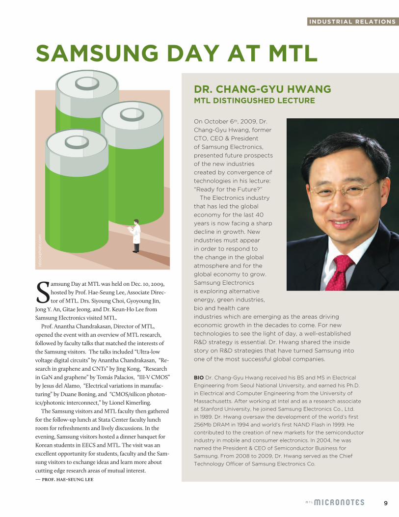
SAMSUNG DAY AT MTL
Samsung Day at MTL was held on Dec. 10, 2009, hosted by Prof. Hae-Seung Lee, Associate Direc-tor of MTL. Drs. Siyoung Choi, Gyoyoung Jin,
Jong Y. An, Gitae Jeong, and Dr. Keun-Ho Lee from Samsung Electronics visited MTL.
Prof. Anantha Chandrakasan, Director of MTL, opened the event with an overview of MTL research, followed by faculty talks that matched the interests of the Samsung visitors. The talks included “Ultra-low voltage digital circuits” by Anantha Chandrakasan, “Re-search in graphene and CNTs” by Jing Kong, “Research in GaN and graphene” by Tomás Palacios, “III-V CMOS” by Jesus del Alamo, “Electrical variations in manufac-turing” by Duane Boning, and “CMOS/silicon photon-ics/photonic interconnect,” by Lionel Kimerling.
The Samsung visitors and MTL faculty then gathered for the follow-up lunch at Stata Center faculty lunch room for refreshments and lively discussions. In the evening, Samsung visitors hosted a dinner banquet for Korean students in EECS and MTL. The visit was an excellent opportunity for students, faculty and the Sam-sung visitors to exchange ideas and learn more about cutting edge research areas of mutual interest. — prof. hae-seung lee
DR. CHANG-GYU HWANGMTL DISTINGUSHED LECTURE
On October 6th, 2009, Dr.
Chang-Gyu Hwang, former
CTO, CEO & President
of Samsung Electronics,
presented future prospects
of the new industries
created by convergence of
technologies in his lecture:
“Ready for the Future?”
The Electronics industry
that has led the global
economy for the last 40
years is now facing a sharp
decline in growth. New
industries must appear
in order to respond to
the change in the global
atmosphere and for the
global economy to grow.
Samsung Electronics
is exploring alternative
energy, green industries,
bio and health care
industries which are emerging as the areas driving
economic growth in the decades to come. For new
technologies to see the light of day, a well-established
R&D strategy is essential. Dr. Hwang shared the inside
story on R&D strategies that have turned Samsung into
one of the most successful global companies.
BIO Dr. Chang-Gyu Hwang received his BS and MS in Electrical
Engineering from Seoul National University, and earned his Ph.D.
in Electrical and Computer Engineering from the University of
Massachusetts. After working at Intel and as a research associate
at Stanford University, he joined Samsung Electronics Co., Ltd.
in 1989. Dr. Hwang oversaw the development of the world’s first
256Mb DRAM in 1994 and world’s first NAND Flash in 1999. He
contributed to the creation of new markets for the semiconductor
industry in mobile and consumer electronics. In 2004, he was
named the President & CEO of Semiconductor Business for
Samsung. From 2008 to 2009, Dr. Hwang served as the Chief
Technology Officer of Samsung Electronics Co.
isto
ckp
hoto
.co
m

10
INDUSTRIAL RELATIONS
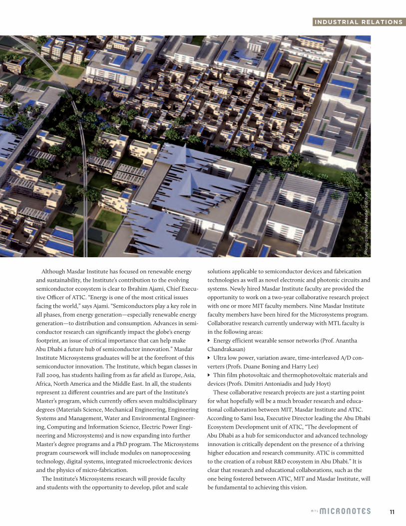
Abu Dhabi is the capital of, and the second largest city in, the United Arab Emirates (UAE). Abu Dhabi possesses approximate-ly 9% of the world’s proven oil reserves and almost 5% of the world’s natural gas reserves. Fueled by this enormous oil and gas wealth, Abu Dhabi has begun a series of economic transforma-tion initiatives aimed at diversifying away from its dependence on fossil fuel revenues and toward a dynamic, knowledge based economy that thrives on competitive rather than comparative advantage. These initiatives include the cultivation of new and emerging industries such as alternative energy, aerospace, and the semiconductor industry.
Central to the development of these industries will be the for-mation of high-technology ecosystems and related human ca-pacity. The Masdar Institute of Science and Technology will be a driving force behind this human capacity development. Masdar Institute is a private, not-for-profit, independent, graduate-level research institute developed with the support and cooperation of MIT’s Technology and Development Program and is the cen-terpiece of Abu Dhabi’s Masdar Initiative. Announced in April 2006, this Initiative is a strategic undertaking by the Abu Dhabi government with the following overarching objectives:
► Economic diversification of Abu Dhabi from a fossil-fuel based economy to a knowledge-based economy
► Positioning Abu Dhabi as a leading developer of advanced technologies
► Positioning of Abu Dhabi as a major contributor towards sustainable human development
Although largely focused on renewable energy and sustain-ability, Masdar Institute began a new Microsystems program in Fall 2010. This program was developed with support from MTL in the areas of academic program development, collaborative research and specification of nano-fabrication equipment for clean room facilities.
Abu Dhabi’s Advanced Technology Investment Company (ATIC) is funding Masdar Institute’s initial clean room equip-ment purchases. ATIC, which was established by the Abu Dhabi government in 2008, is a specialist investment company focused on the establishment of a global advanced technology sector in Abu Dhabi. ATIC’s partnership with Masdar Institute is just one of its many activities aimed at establishing a semiconductor industry in Abu Dhabi. These activities were catalyzed last year by ATIC’s joint venture with Advanced Micro Devices (AMD) to spin off AMD’s manufacturing arm into GlobalFoundries, now the world’s third-largest semiconductor manufacturing com-pany. Over a five year period, ATIC will create a semiconduc-tor ecosystem in Abu Dhabi and at the heart of this ecosystem will be a state-of-the-art GlobalFoundries fabrication facility. Although no ecosystem exists in Abu Dhabi as of yet, a 3 sq km tract of land next to Abu Dhabi International Airport has been identified for the planned semiconductor cluster.
MIT & MASDAR INSTITUTE DEVELOP MICROSYSTEMS EDUCATION & RESEARCH IN THE MIDDLE EASTby prof. steve griffiths, executive director of institute initiatives, masdar institute of science and technology; formerly executive director, mit/abu dhabi program
11
INDUSTRIAL RELATIONS
Although Masdar Institute has focused on renewable energy and sustainability, the Institute’s contribution to the evolving semiconductor ecosystem is clear to Ibrahim Ajami, Chief Execu-tive Officer of ATIC. “Energy is one of the most critical issues facing the world,” says Ajami. “Semiconductors play a key role in all phases, from energy generation—especially renewable energy generation—to distribution and consumption. Advances in semi-conductor research can significantly impact the globe’s energy footprint, an issue of critical importance that can help make Abu Dhabi a future hub of semiconductor innovation.” Masdar Institute Microsystems graduates will be at the forefront of this semiconductor innovation. The Institute, which began classes in Fall 2009, has students hailing from as far afield as Europe, Asia, Africa, North America and the Middle East. In all, the students represent 22 different countries and are part of the Institute’s Master’s program, which currently offers seven multidisciplinary degrees (Materials Science, Mechanical Engineering, Engineering Systems and Management, Water and Environmental Engineer-ing, Computing and Information Science, Electric Power Engi-neering and Microsystems) and is now expanding into further Master’s degree programs and a PhD program. The Microsystems program coursework will include modules on nanoprocessing technology, digital systems, integrated microelectronic devices and the physics of micro-fabrication.
The Institute’s Microsystems research will provide faculty and students with the opportunity to develop, pilot and scale
solutions applicable to semiconductor devices and fabrication technologies as well as novel electronic and photonic circuits and systems. Newly hired Masdar Institute faculty are provided the opportunity to work on a two-year collaborative research project with one or more MIT faculty members. Nine Masdar Institute faculty members have been hired for the Microsystems program. Collaborative research currently underway with MTL faculty is in the following areas:
► Energy efficient wearable sensor networks (Prof. Anantha Chandrakasan)
► Ultra low power, variation aware, time-interleaved A/D con-verters (Profs. Duane Boning and Harry Lee)
► Thin film photovoltaic and thermophotovoltaic materials and devices (Profs. Dimitri Antoniadis and Judy Hoyt)
These collaborative research projects are just a starting point for what hopefully will be a much broader research and educa-tional collaboration between MIT, Masdar Institute and ATIC. According to Sami Issa, Executive Director leading the Abu Dhabi Ecosystem Development unit of ATIC, “The development of Abu Dhabi as a hub for semiconductor and advanced technology innovation is critically dependent on the presence of a thriving higher education and research community. ATIC is committed to the creation of a robust R&D ecosystem in Abu Dhabi.” It is clear that research and educational collaborations, such as the one being fostered between ATIC, MIT and Masdar Institute, will be fundamental to achieving this vision.
Pho
to c
our
tesy
Mas
dar
Inst
itut
e

12
EVENT REPORT
For the past 20 years, the MTL Annual Research Con-ference (MARC) has allowed MTL students, faculty, staff, and industry members to come together to share
their research achievements. This year, we had another successful MARC with nearly 200 attendees. Many faces were familiar, but the location was new, as it was the first time that MARC was held at the Cambridge Marriott Ho-tel. Along with the new local venue, new activities were introduced such as the King’s Back Bay kick-off reception, which was held in Boston the night before MARC. The at-tendees enjoyed mingling while playing pool and games.
Early next morning, MARC was in full swing with a keynote presentation by Dr. Jun’ichi Sone, VP of NEC Central Research Laboratories. Dr. Sone’s presentation focused on energy and technology, which is an active area of research at MTL. He described how nanotechnol-ogy can be used to reduce electric power consumption and lead to a more environmentally sustainable society.
Following the keynote speech was the core event of MARC: the technical presentations. This year’s program featured 69 technical presentations divided into four sessions: Elec-tronic and Photonic Devices, MEMS and BioMEMS, Circuits and Systems, and Nanotechnology and Energy Applications. Presenters highlighted their research in rapid 90-second talks which packed information with occasional creativity and entertainment. The presenters later answered questions at poster sessions, where a new activity named “Poster Hunt!” was introduced. “Poster Hunt!” encouraged attendees to complete crosswords by searching for technical clues on post-ers. The activity was an overwhelming success as it enhanced the exposure of research work while making the experience fun for the attendees. Finally, the conference came to a close with a banquet and an entertaining awards ceremony that involved lasers, a wheel of fortune, and smiling awardees.
Congratulations to the winners of this year’s presentation awards, which were generously donated by Texas Instruments:
MARC2010by david he • marc2010 co-chair
► Will Chung ► Han Wang ► Meekyung Kim ► Rumi Chunara ► Hansen Bow
► Bonnie Lam ► Patrick Mercier ► Marcus Yip ► Gilbert Nessim ► Carlijn Mulder
ABOVE MARC2010 co-chairs Vanessa Wood (left) and David He (right). (Photo, Paul McGrath)
ABOVE MARC Keynote Speaker Jun'ichi Sone of NEC (left) addresses the audience with MARC2010 Faculty Chair Prof. Joel Voldman (right). (Photo, Paul McGrath)
ABOVE Attendees, including Prof. Judy Hoyt (center) enjoy the lunch buffet at MARC2010. (Photo, Paul McGrath)

13
EVENT REPORT
ENERGY RESEARCHERSFIND OBAMA AN EAGER STUDENTPresident showed keen interest, quick understanding and warm appreciation, say his hosts
by david l. chandler • mit news office
During a tour of MIT labs prior to his talk at Kresge Auditorium in October 2010, President Barack Obama saw demonstrations of several clean-energy technologies being developed at MIT: batteries that can be self-assembled by genetically engineered viruses; long-lasting high-efficiency light bulbs; windows that can double as solar energy collectors; and structures that could provide offshore windmills with built-in power storage.
The tour marked the first time a sitting president has visited MIT’s laboratories to see demonstrations of ongoing research work and meet with faculty members who are conducting that research. The five faculty members who made the presentations to the President, along with some of their students, gathered in two labs in Building 13, with posters describing their work and demonstrations to show the technology in action.
‘A LITTLE NERVOUS’
Marc Baldo, the Esther and Harold E. Edgerton Associate Professor of Electrical Engineering, demonstrated technology for concentrating solar energy systems using coated glass. Baldo said Obama was curious and asked a few questions about the research.
“It seemed like he had a really good time, that he actually found the whole experience quite stimulating,” Baldo said “I was a little nervous, but I got the impression that he’s used to walk-ing into rooms full of nervous people, and he just put everyone at ease.”
“His demeanor was very inquisitive and playful,” said Vladimir Bulovic, the KDD Associate Professor of Communications and
Technology, who demonstrated high-efficiency, long-lasting light bulbs based on quantum dot technology. When Bulovic showed him some of the equipment used to manufacture the lights, including a vacuum chamber that produces a harder vacuum than would be found in space between the Earth and the moon, Obama asked him, “When one of these pieces of equipment breaks, who do you call?” Bulovic explained that the equipment is all custom built at MIT, and he and his colleagues and students are the “glorified car mechanics” who have to fix anything that breaks.
“I believe that the president knew what my answer would be and that he wanted to give me a chance to vocalize the resource-fulness of MIT engineers in front of the national press,” Bulovic added.
A PRESIDENTIAL SEAL OF APPROVAL
Before the president left the lab, Bulovic, at the request of some of his students, asked if the President would be willing to “me-morialize the moment.” He was standing next to a control panel for some equipment that many of the students use almost daily.
“He graciously did sign it,” he said, “and added ‘Great work!’ up at the top.” Since he had already seen all of the other presentations at that point, Bulovic said he and his students interpreted that
“as a message to all of us, that he was impressed by all the work he saw. It was a message to the entire MIT community.”
Bulovic was impressed with Obama’s “eagerness to absorb more information on what science can do for us.” The whole experience, he said, was “overwhelming and humbling.”
ABOVE Detail of President Barack Obama's signature on an instrument in the Bulovic lab. (Photo courtesy of Bulovic lab)

14
IN THE NEWS
Among this year's honorees in the MIT School of Engi-neering's 10th annual Infinite Mile Awards were MTL's Computation team of Mike Hobbs, Tom Lohman and Bill Maloney (pictured right, left to right).
The Infinite Mile Awards are meant to recognize mem-bers of the school's administrative staff, support staff, service staff and sponsored research staff. The awards support the Institute's and the school's objectives for excel-lence. Among this year's honorees were MTL's Computa-tion team of Mike Hobbs, Tom Lohman and Bill Maloney.
Since their inception in 2001, the School of Engineering's Infinite Mile Awards have been presented to more than 150 staff members in the school. Nominations for Infinite Mile Awards are made by department heads and laboratory directors in the School of Engineering. They are presented to individuals and teams whose work is of the highest quality. They stand out because of their high level of commitment and because of the enormous energy and enthusiasm they bring to their work.
The citation for the MTL team, read by Eileen Ng-Ghavidel at the ceremony, shared stories of the team's responsiveness, professionalism, and flexibility: "The MTL community is truly fortunate to have this wonderful team that ensures smooth computing operations. They are knowledgeable, talented, and, when it counts most, they are remarkably resourceful."
Past Infinite Mile Award winners from MTL include Debroah Hodges-Pabon (2002), Carolyn Collins (2005), Samuel Crooks and Vicky Diadiuk (2006), Kurt Brod-erick (2007), Rhonda Maynard (2007), and the team of Dan Adams, Ryan O’Keefe and Tim Turner (2009).
EECS faculty member and principal investigator in the Microsystems Technology Laboratories
(MTL) Tomás Palacios has been selected by the International Symposium on Compound Semiconductors (ISCS) committee to win the ISCS Young Scientist Award. He is cited for contribu-tions to the development of mm-wave GaN high electron mobil-ity transistors and their integration with silicon electronics.
The ISCS Young Scientist Award was initiated in 1986, and the recipients have been selected by the International Symposium on Compound Semiconductors Award Committee for technical achievements in the field of compound semiconductors made by a scientist under the age of forty.
Palacios received the ISCS award on June 3, 2010 at the open-ing session of the ISCS 2010 in Kagawa, Japan. P
hoto
co
urte
sy T
om
�s P
alac
ios
Pho
to, G
ary
Rig
go
tt
SCHOOL OF ENGINEERING AWARDS MTL COMPUTE TEAM FOR 'TEAM EXCELLENCE'
PALACIOS RECEIVES ISCS YOUNG SCIENTIST AWARD

15
IN THE NEWS
WEINSTEIN RECEIVES DARPA YOUNG FACULTY AWARD
Dana Weinstein, a core faculty member of the Microsystems Technology Laboratories at MIT, received the 2010 Young Faculty Award from the Defense Advanced Research Projects Agency (DARPA) on April 22, 2010. DARPA's Defense Sciences Office grants this award annually to junior faculty conducting research in the areas of the physical sciences, engineering and mathematics. The award is administered by DARPA's Defense Sciences Office and Microsystems Technology Office. Weinstein and her MIT research group, the Hybrid Devices Lab, are working to develop innovative technologies for more-than-Moore devices. Their focus is on developing NEMS-enhanced electron devices to achieve high-Q, small footprint resonators at previously inaccessible frequencies with the capacity for direct integration in standard CMOS processes. Weinstein's group has demonstrated acoustic resonance in Silicon-based Independent Gate FinFETs at multi-GHz frequencies with frequency-quality factor products rivaling those of quartz. Investigation of fundamental limits of this technology and exploration into device optimization, integration, and control will provide circuit designers with basic building blocks for RF and mm-wave applica-tions, including wireless communication, high-accuracy frequency sources for timing applica-tions and navigation, and integrated temperature sensing in CMOS.
PAUL GRAY NAMED 2010 IEEE FOUNDERS MEDAL RECIPIENTMIT President Emeritus Paul E. Gray has been named the recipient of the 2010 IEEE Founders Medal in recognition of his "exemplary career of leadership in education, research and public policy," the IEEE, the world's largest technical professional association, announced in December 2009.
Pho
to, P
atsy
Sam
pso
n
MTL TEAM WINS AWARD FOR TINY STEAM GENERATOR
A research team from the Microsystems Technology Laboratories (MTL) at MIT received an award for Best Oral Presentation at the 2009 International Workshop on Micro and Nanotechnology for Power Generation and Energy Conversion Applications (PowerMEMS). The workshop, which was held from December 1-4, 2009 in College Park, MD, is an annual event for researchers around the world specializing in power conversion and energy generation research using micro- and nano-electro-mechanical systems (or MEMS/NEMS). The team consists of Mechanical Engineering Professor Carol Livermore, MTL Principal Scientist Dr. Luis Fernando Velasquez-Garcia, and Mechanical Engineering doctoral candidate Feras Eid. Their paper was titled "Design, Fabrication and Demonstration of a MEMS Steam Generator for Ejector Pump Applications."

16
RESEARCH NEWS
MECHANICAL DEVICES STAMPED ON PLASTICMicroelectromechanical devices gave us the Wii and the digital movie projector.
MIT researchers have found a new way to make them.
by larry hardesty • mit news office
Microelectromechanical devices—tiny machines with moving parts—are everywhere these days: they monitor air pressure in car tires, register the gestures of video game players, and reflect light onto screens in movie theaters. But they’re manufactured the same way computer chips are, in facilities that can cost billions of dollars, and their rigidity makes them hard to wrap around curved surfaces.MTL researchers have discovered a way to make microelectro-mechanical devices, or MEMS, by stamping them onto a plastic film. That should significantly reduce their cost, but it also opens up the possibility of large sheets of sensors that could, say, cover the wings of an airplane to gauge their structural integrity. The printed MEMS are also flexible, so they could be used to make
sensors with irregular shapes. And since the stamping process dis-penses with the harsh chemicals and high temperatures ordinarily required for the fabrication of MEMS, it could allow MEMS to incorporate a wider range of materials.Conventional MEMS are built through a process called photo-lithography, in which different layers of material are chemically deposited on a substrate — usually a wafer of some semiconduct-ing material — and etched away to form functional patterns. Since a wafer is at most 12 inches across, arranging today’s MEMS into large arrays requires cutting them out and bonding them to some other surface.Instead of using a wafer, the MIT researchers begin with a grooved sheet of a rubbery plastic, which is coated with the elec-
THIS PAGE Unlike existing micromachines, the researchers' gold films are flexible, so they could be used to coat irregular surfaces.Photo: Corinne Packard

17
RESEARCH NEWS
trically conductive material indium tin oxide. The researchers use what they call a “transfer pad” to press a thin film of metal against the grooved plastic. Between the metal film and the pad is a layer of organic molecules that weaken the metal’s adhesion to the pad. If the researchers pull the pad away fast enough, the metal remains stuck to the plastic.“It’s kind of similar to if you have Scotch tape on a piece of paper,” says Corinne Packard, a postdoc in the Research Lab of Electron-ics at MIT who led the work, along with professors of electrical engineering Vladimir Bulović and Martin Schmidt. “If you peel it off slowly, you can delaminate the tape very easily. But if you peel fast, you’ll rip the paper.”Once the transfer pad has been ripped away, the metal film is left spanning the grooves in the plastic like a bridge across a series of ravines. Applying a voltage between the indium-tin-oxide coating and the film can cause it to bend downward, into the groove in the plastic: the film becomes an “actuator” — the moving part in a MEMS. Varying the voltage would cause the film to vibrate, like the diaphragm of a loudspeaker; selectively bending differ-ent parts of the film would cause them to reflect light in different ways; and dramatically bending the film could turn a smooth surface into a rough one. Similarly, if pressure is applied to the metal film, it will generate an electric signal that the researchers can detect. The film is so thin that it should be able to register the pressure of sound waves.
SERENDIPITY
The discovery of the manufacturing technique, which the MIT team describes in a forthcoming issue of the journal Advanced Materials, was a happy accident. The researchers were actually trying to use a printing technique to build an electrical circuit. They had created a plastic stamp with a pattern molded into it
ABOVE: To test a new technique for creating micromachines, MIT researchers deposited films of gold on a sheet of plastic; grooves in the plas-tic are visible as a series of horizontal lines.Image: Corinne Packard and Apoorva Murarka
and were trying to transfer that pattern to a thin silver film. They had expected that the plastic would pull away the silver it made contact with, leaving behind an electrode that could control an organic light-emitting diode.Instead, however, the stamp kept pulling away the entire silver film. “The first couple times we did this, we were like, ‘Ah! Bum-mer, man,’” says Bulović. “And then a light bulb went off, and we said, ‘Well, but we just made the world’s first printed MEM.’” The stamp was intended as a means of creating an electronic device; instead, it ended up serving as the basis for a device itself. The researchers’ ensuing work was on the ideal architecture for the device and on ways to minimize the metal film’s adhesion to the transfer pad and maximize its adhesion to the grooved plastic.Because the researchers hadn’t set out to make MEMS, and be-cause, to their knowledge, their films constitute the first stamped MEMS devices, they’re still trying to determine the ideal applica-tion of the technology. Sheets of sensors to gauge the structural integrity of aircraft and bridges are one possibility; but the MEMS could also change the physical texture of the surfaces they’re applied to, altering the airflow over a wing, or modifying the reflective properties of a building’s walls or windows. A sheet of thousands of tiny microphones could determine, from the differ-ence in the time at which sound waves arrive at different points, where a particular sound originated. Such a system could filter out extraneous sounds in a noisy room, or even perform echolocation, the way bats do. The same type of sheet could constitute a paper-thin loudspeaker; the vibrations of different MEMS might even be designed to interfere with each other, so that transmitted sounds would be perfectly audible at some location but inaudible a few feet away. The technology could also lead to large digital displays that could be rolled up when not in use.John Rogers, a researcher at the University of Illinois at Urbana-Champaign who has pioneered techniques for printable electrical circuits, is particularly intrigued by the idea that printable MEMS could incorporate materials that are incompatible with existing MEMS manufacturing processes. “The ability to do heterogeneous integration of different material types into micromachines is a neat capability that would be enabled by this form of manufactur-ing,” Rogers says. “It opens up new design opportunities because it relaxes constraints on choices of materials.” And in general, Rog-ers says, the idea of printing MEMS is “cool.” “What they’ve done in this paper is demonstrated, for the first time, to my knowledge, this kind of concept.”

18
RESEARCH NEWS
STRAINING FORWARDNanowires made of ‘strained silicon’— silicon whose atoms have been pried slightly apart — show how to keep increases in computer power coming.
by larry hardesty • mit news office
Computers keep getting more powerful because silicon transis-tors keep getting smaller. But that miniaturization can’t con-tinue much further without a change to the transistors’ design, which has remained more or less the same for 40 years.One potential successor to today’s silicon transistors is silicon nanowires, tiny filaments of silicon suspended like the strings of a guitar between electrically conducting pads. But while silicon nanowires are certainly small enough to keep the miniaturiza-tion of computer circuitry on track, there’s been doubt about whether they can pass enough electrical current for high-speed computing. At 2008’s International Electron Device Meeting, researchers at MIT’s Microsystems Technology Laboratories demonstrated silicon nanowires with twice the electron mobil-ity — which indicates how easily current can be induced — of their predecessors. Now, the same group has shown that they can build chips in which up to five high-performance nanowires are stacked on top of each other. That would allow nanowire transistors to pass up to five times as much current without tak-ing up any more area on the surface on the chip, a crucial step toward establishing the viability of silicon-nanowire transistors.
A transistor is basically a switch: when it’s on, it passes an electrical current, and when it’s off, it doesn’t. Flipping the switch requires charging a part of the transistor called the “gate.” In today’s design, the gate sits on top of the transistor. But if
the transistor gets small enough, electricity will leak across it whether the gate is charged or not. Turning the switch off becomes impossible.
Because silicon nanowires are suspended in air, the gate can be wrapped all the way around them, like insulation around an electrical wire, which improves control of the switch. But the narrowness of the nanowires limits the amount of current they can pass.
Electrical-engineering professor Judy Hoyt and her graduate students Pouya Hashemi and Leonardo Gomez improved the performance of silicon-nanowire transistors by, basically, prying the atoms of the silicon slightly farther apart than they would be naturally, which allows electrons to flow through the wires more freely. Such “strained silicon” has been a standard way to improve the performance of conventional transistors since 2003. But Hoyt was one of the early researchers in the field.
“Starting in the early 1990s, she’s really played a pioneering role in strained-silicon technology,” says Tahir Ghani, director of transistor technology and integration for Intel’s Technology and Manufacturing Group. “She did a lot of this pioneering work that for the first time demonstrated that you can have significant performance gains by implementing strain into silicon technology.” Hoyt and her group’s work on strained-silicon nanowires, Ghani says, “combines the two key elements
RIGHT: Five different test structures feature stacks of nanowires with different numbers of levels. The bottom structure has only one level; the top structure has five. The length of the nanowires is 1.4 µm.Images: Judy Hoyt, Pouya Hashemi and Leonardo Gomez

19
RESEARCH NEWS
of transistors” — performance and space efficiency — “both of which are very key to scaling in the future. And so from that standpoint, it makes it very relevant for industry.”
HANDLING STRESS
To build their stacked nanowire transistors, the MIT research-ers begin with a normal silicon wafer, on which they deposit a silicon-germanium composite. Because germanium atoms are bigger than silicon atoms, the distances between atoms in the silicon-germanium layer are greater than they would be in a layer of pure silicon. When the researchers deposit another layer of silicon on top of the composite, the silicon atoms try to align themselves with the atoms beneath them, so they, too, end up spaced slightly farther apart.
This layer of strained silicon is bound to a second silicon wa-fer, and the other layers are removed, leaving the second wafer covered with a base layer of strained silicon. The researchers then stack alternating layers of silicon-germanium and silicon on top of the base layer, passing its strain on to each successive layer of silicon. Using a technique called electron-beam lithogra-phy, the researchers pattern fine lines onto the stacks and then etch away the material between the lines. Finally, they etch away the remaining silicon-germanium, and they’re left with several layers of suspended silicon nanowires. Hoyt and her students have manufactured nanowires with a diameter of only eight nanometers, which they described in a 2009 paper in the IEEE journal Electron Device Letters; by contrast, the smallest elements of today’s computer chips are 45 nanometers across.
Hoyt says that her group can create silicon with two times the strain seen in chips built by commercial vendors. “We increase the germanium fraction of the initial layer, so we therefore build more stress into the silicon,” Hoyt says. Moreover, says Hash-emi, “we are the only group in the world that has demonstrated that we can maintain this strain after suspension” — that is, once the underlying layers have been cut away.
So far, Hoyt’s group has built nanowire transistors in which charge is carried by moving electrons. But to maximize com-putational efficiency, a standard computer chip in fact uses two types of transistors. In the other type, charge is carried by so-called holes. A hole is simply the absence of an electron in a crystal of semiconducting material. When an electron slides over to fill the hole, it vacates its own spot in the crystal; another electron slides over to fill that spot; and so on. In this way, the hole in effect moves along the length of the crystal.
Increasing the mobility of holes in such transistors requires a different type of strain: the atoms of the crystal actually have to be jammed closer together than is comfortable. So Hoyt’s group is now working to build nanowires from a silicon-germanium composite, where intervening layers of pure silicon cause com-pression rather than tension.
FROM TOP TO BOTTOM, four successive magnifications of a test chip with nanowire circuits. (1) A wafer with dozens of chips etched into it. (2) A close-up of four chips. (3) Cross sections of two nanowires in a transistor: at the centers are the nanowires; surrounding them are the transistor elements called “gates.” (4) A close-up of the wire with diameter of 8 nm..Images: Judy Hoyt, Pouya Hashemi and Leon-ardo Gomez

20
RESEARCH NEWS
TWO CHIPS IN ONE MIT team finds a way to combine
materials for semiconductor manufacture. The advance helps
address the limitations of conventional silicon microprocessors by david l. chandler • mit news office
For decades, researchers have been trying to combine semicon-ductor materials that have different and potentially comple-mentary characteristics into a single microchip. Now, an MIT team has finally succeeded in this effort, an advance that could point to a way of overcoming fundamental barriers of size and speed facing today's silicon chips.
The standard semiconductor material for most of today's computer chips is silicon, and the main way engineers have im-proved the speed of silicon chips so far is to keep making them smaller. But silicon chips are now approaching their fundamen-tal size limits, says Tomás Palacios, assistant professor in the De-partment of Electrical Engineering and Computer Science. "We won't be able to continue improving silicon by scaling it down for long," he says. "It's very difficult to make them a lot smaller."
One way around the size limitation is to use new advanced materials for the transistors. "There are several semiconductor materials that offer better performance than silicon," Palacios says. "The problem is, even though they allow for very fast tran-sistors, they cannot compete with silicon in terms of integra-tion and scalability."
A present-day silicon microprocessor chip may contain more than a billion identical transistors, but researchers run into problems when they try to make similar large numbers of tran-sistors using new materials. "They can make one, 10 or even a few hundred that are really fast," Palacios says, but find it very difficult to make them in larger quantities. Companies have spent decades and billions of dollars building up the technology for making silicon chips efficiently and reliably. Given that long and expensive development process, it's hard for any new mate-rial to catch up and be competitive, Palacios says.
TWO MATERIALS, ONE CHIPBut it turns out that most of those transistors on a chip — for example, ones used to store information in the chip memory — don't really need to perform at maximum speed. Only a much smaller number, 5 to 10 percent of the total, are actually carrying out the computations and need to be as fast as possible, he says.
The solution that Palacios and his graduate student, Will Chung, developed is one that many other researchers have tried unsuccessfully to achieve: combining two different kinds of materials on a single, hybrid chip. Conventional silicon would provide the vast majority of the transistors, while a different semiconductor material with better performance would be used for the transistors that need to work faster.
Palacios and Chung created a chip that combines silicon transistors on the same wafer with ones made from gallium nitride, a semiconductor material that has a much better per-formance than silicon. The results were initially presented in June at the Device Research Conference in Pennsylvania, and are being published in the October issue of the IEEE journal Electron Device Letters.
Instead of trying to grow the high-performance semiconduc-tor material on top of a silicon chip as others have attempted, Palacios and Chung made the new hybrid chip by embedding a gallium nitride layer into the same type of silicon substrate that is used by the silicon electronics industry. This not only pro-duces a faster chip, but one that is highly efficient (having most of the transistors operate at slower speeds means that the chips do not consume too much energy). Moreover, the chips can be manufactured using the standard technology currently used for commercial silicon chips.
ADVANTAGES AND CHALLENGESThomas Kazior, technical director of Advanced Microelectron-ics Technology at Raytheon Integrated Defense Systems, says the new advance addresses some of the present limitations of both silicon and gallium nitride technology. This could "enable a new class of high-performance mixed-signal and digitally controlled RF [radio frequency] circuits for use in a wide range of Department of Defense and commercial applications," he says. Besides microprocessor chips, the new integrated technol-ogy can be used for other applications such as hybrid chips that combine lasers and electronic components on a single chip, and energy-harvesting devices that can harness the pressure and vibrations from the environment to produce enough power to run the silicon components.
Such hybrid chips could also lead to much more efficient cell phone manufacturing, Palacios says. Present-day cell phones generally use at least four or five separate chips made from different semiconductor materials, "With this technology, you could potentially integrate all these functions on a single chip."
Raytheon's Kazior agrees, saying this technology "provides a path to RF 'systems on a chip.'" At present, the new technique has been used to make chips that are about one square inch in size. Conventional chip manufacturing processes typically use larger wafers, 8 or 12 inches in diameter, so the research now is focused on overcoming the difficulties of scaling up the process to produce these larger chips, without sacrificing quality. "We have several ideas in that direction," Palacios says. "We are al-ready discussing with several companies how to commercialize this technology and fabricate more complex circuits." However, it could take a couple of years to get to the point where it could be commercialized, he says.
Kazior says "To be truly usable this technology needs to be scaled to larger-wafer diameters. In addition, challenges of device reliability and thermal management of the high-power [gallium nitride] transistors need to be addressed."
The research was funded by the DARPA Young Faculty Award, the MARCO Interconnect Focus Center and the MIT Desh-pande Center. Device fabrication was carried out at the Mi-crosystems Technology Laboratories and the Nano-Structures Laboratory at MIT.
THIS PAGE Graduate student Will Chung displays a hybrid chip being developed in Professor Tomás Palacios' lab. The machine in the background is used to combine the semiconductor materials into one chip. Photo, Patrick Gillooly

21
RESEARCH NEWS
SELLING CHIP MAKERS ON OPTICAL COMPUTING MTL researchers show that computing with light isn’t so far fetched.
by larry hardesty • mit news office
Computer chips that transmit data with light instead of electric-ity consume much less power than conventional chips, but so far, they’ve remained laboratory curiosities. Professors Vladimir Stojanović and Rajeev Ram and their colleagues in MIT’s Re-search Laboratory of Electronics and Microsystems Technology Laboratories hope to change that, by designing optical chips that can be built using ordinary chip-manufacturing processes.
“I don’t see anyone else that’s doing that,” says Michael Watts, a researcher at Sandia National Laboratories who’s also working on optical chips. “If they’re successful at that, then convincing a major processor or memory manufacturer that this is a viable approach will be much, much easier.” Granted access to the same manufacturing facilities that Texas Instruments uses to produce cell phone chips and microprocessors, the MIT researchers have demonstrated that they can put large numbers of working opti-cal components and electronics on the same chip. But so far, the electronics haven’t been able to control the optics directly. That’s something that Stojanović hopes to show with a new batch of chips due back from TI and another major semiconductor manufacturer this winter.
Optical data transmission could solve what will soon be a pressing problem in chip design. As chips’ computational capac-ity increases, they need higher-bandwidth connections to send data to memory; otherwise, their added processing power is wasted. But sending more data over an electrical connection requires more power.
Smaller transistors are more energy-efficient than larger ones, so over time, chips’ total power consumption has changed little. But “the fraction of power that’s used for communications has grown,” Watts says. “At some point, you have to devote all your power to communications. And that point is not too far off. And then what’s left for computation? Nothing.” Future chips could simply draw more power, but then they would also be harder to cool, and the battery life of laptops and handheld devices would dramatically shorten.
So chip companies would welcome a more energy-efficient way to move data around—if they were confident that it was cost-effective. And that’s why demonstrating compatibility with existing manufacturing processes would be so persuasive.
Manufacturers build chips by sequentially depositing layers of different materials—like silicon, silicon dioxide, and copper—on a wafer of silicon, and then etching the layers away to build three-dimensional structures. The problem with using existing processes to build optical components is that the deposition lay-ers are thinner than would be ideal. “You would want a normal photonic device to be a little bit taller and thinner so that you can minimize the surface-roughness losses,” Stojanović says.
“Here you don’t have that choice because the film thicknesses are set by fabrication.”
Optical chips use structures called waveguides to direct light, and researchers trying to add optical components to a silicon chip usually carve the waveguides out of a single crystal of sili-con, Stojanović says. But waveguides made from single-crystal
silicon require insulating layers above and below them, which standard chip-manufacturing processes like TI’s and Intel’s provide no way to deposit. They do, however, provide a way to deposit insulators above and below layers of polysilicon, which consists of tiny, distinct crystals of silicon clumped together and is typically used in the part of a transistor called the gate. So the MIT researchers built their waveguides from polysilicon instead.
So far, TI has produced two sets of prototypes for the MIT researchers, one using a process that can etch chip features as small as 65 nanometers, the other using a 32-nanometer process. To keep light from leaking out of the polysilicon waveguides, the researchers hollowed out the spaces under them when they got the chips back — the sole manufacturing step that wasn’t possible using TI’s in-house processes. But “that can probably be fixed more elegantly in the fabrication house if they see that by fixing that, we get all these benefits,” Watts says. “That’s a pretty minor modification, I think.”
The MIT researchers’ design uses light provided by an off-chip laser. But in addition to guiding the beam, the chip has to be able to load information onto it and pull information off of it. Both procedures use ring resonators, tiny rings of silicon carved into the chip that pull light of a particular frequency out of the waveguide. Rapidly activating and deactivating the resonators effectively turns the light signal on and off, and bursts of light and the gaps between them can represent the ones and zeroes of digital information.
To meet the bandwidth demands of next-generation chips, however, the waveguides will have to carry 128 different wavelengths of light, each encoded with its own data. So at the receiving end, the ring resonators provide a bank of filters to disentangle the incoming signals. On the prototype chips, the performance of the filter banks was “the most amazing result to us,” Stojanović says, “which kind of said that, okay, there’s still hope, and we should keep doing this.” The wavelength of light that the resonators filter is determined by the size of their rings, and no one — at either TI or MIT — could be sure that conven-tional manufacturing processes were precise enough to handle such tiny variations.
Stojanović hopes that the next batch of prototypes, which should give the chips’ electronics control over the optical com-ponents, will demonstrate that the resonators perform as well when loading data onto light beams. At the same time, the team is looking to extend its approach to memory chips. “The memo-ry’s a much tougher nut to crack, because it is such a cost-driven business, where every process step matters,” Stojanović says.
“Things are a lot harder to change there, and optics really needs to be absolutely compatible with process flow.” But if memory chips as well as processors sent data optically, Stojanović says, then in addition to saving power, they could make computers much faster. “If you just focus on the processor itself, you maybe get a 4x advantage with photonics,” Stojanović says. “But if you focus on the whole connectivity problem, we’re talking 10, 20x improvements in system performance.”
THIS PAGE In the prototype optical chip shown here, the circles in the top two rows are "ring resonators" that can filter out light of different wave-lengths. Image courtesy of Vladimir Stojanović.

22
RESEARCH NEWS
LIFE AFTER SILICON Researchers in MTL are making the case for the use of exotic
materials to help microchips keep improving by larry hardesty • mit news office
The huge increases in the power and capacity of computers, cell phones and communications networks in the last 40 years have been the result of ever-shrinking silicon transistors. But silicon transistors are now getting so small that they’re run-ning up against fundamental physical limits: soon, it will be impossible to squeeze any better performance out of them. Researchers in MIT’s Microsystems Technology Laboratories, led by professor of electrical engineering Jesús del Alamo, have been investigating whether transistors made from more exotic materials can keep the processing power coming. At the 2010 International Electron Devices Meeting in Balti-more—the premier conference on microelectronics—they presented four separate papers offering cause for hope.
Del Alamo’s group works with compound semiconductors, so called because, unlike silicon, they’re compounds of several other materials. In particular, the group works with materials that com-bine elements from columns III and V of the periodic table and have names like gallium arsenide and indium gallium arsenide.
Electrons travel through these so-called III-V materials much more rapidly than they do through silicon, and III-V semicon-ductors have been used for years in high-speed electronics, such as the devices that process data in fiber-optic networks. But according to del Alamo, the transistors in III-V optical components are “larger by several orders of magnitude” than the transistors in computer chips. Whether they can main-tain their performance advantages at dramatically smaller scales is the question that del Alamo’s group is tackling.
In a computer chip, transistors serve as on-off switches that help execute logic operations — comparing two values, for instance, or performing arithmetic functions. But transis-tors can also be used to amplify electrical signals — as they do in transistor radios. Last year, del Alamo’s group built a III-V transistor that set a world record for high-frequency opera-tion, meaning that it was able to amplify higher-frequency signals than any previous transistor. While that gives some sense of the transistor’s capacities, two of the four papers presented in Baltimore assess properties of the transis-tor that better predict its performance as a logic element.
To measure those properties, del Alamo says, the group built chips with multiple transistors that were identical except for the length of their most critical element, called the gate. If a transistor is a switch, the gate is what throws it. When the gate is electrically charged, it exerts an electrostatic force on a semiconductor layer beneath it; that force is what determines whether the semiconductor can conduct electricity or not.
By comparing the performance of transistors with different gate lengths at different frequencies, del Alamo’s group was able to extract precise measurements of both the velocity of the electrons passing through the transistor and the electro-static force that the gate exerted on the semiconductor layer.
Electron velocity, del Alamo says, is the “key velocity that is going to set the performance of a future logic switch based
LEFT A test chip used to evaluate the per-formance of indium gallium arsenide in logic circuits. Image courtesy of the del Alamo group
on these kinds of materials, and we have obtained veloci-ties that are easily two and a half times higher than the best silicon transistors made today.” While the electrostatic force exerted by the gate was lower than the researchers had hoped, measuring it so precisely allowed del Alamo’s group to de-velop better physical models of III-V transistors’ behavior. On the basis of those models, del Alamo says, he believes that the gate’s performance is a “manageable problem.”
“Before the industry is willing to switch from one technol-ogy to the next technology, people in the industry would want to make sure that they were making the right bet, the right investment,” says Robert Chau, a senior fellow at chip giant Intel who has worked closely with del Alamo’s group. “So obviously, people will need to thoroughly under-stand the physics behind this proposed new technology. I think that’s what Professor del Alamo’s group has been do-ing — getting to the science of the device operation.”
The third paper is in a similar vein, a collaboration with researchers at Purdue University who have developed simula-tors to model the performance of III-V transistors that are even smaller than the MIT prototypes. Del Alamo’s group used its precise measurements of the prototypes’ performance to help the Purdue team calibrate its simulator. The fourth paper, however, addresses a different topic: it proposes a new design for III-V transistors that, del Alamo says, will work better at smaller scales, because it permits a thinner layer of material to separate the gate and the semiconductor material beneath it.
For all their speed, III-V semiconductors have a disadvantage as a next-generation chip material: they’re rarer, and therefore more expensive, than silicon. But while the MIT prototypes were built entirely with III-V materials, del Alamo envisions “a silicon-like technology where just under the gate … you take silicon out and stick in indium gallium arsenide. It’s a minute amount of material that is required in every transistor to make this happen.” Indeed, “III-V is not really in competition with silicon,” Chau agrees. “It still will be a silicon transistor. It’s just that you’re using this non-silicon element to make it even better.”

23
RESEARCH NEWS
SELF-POWERED SENSORS Harvesting electricity from
small temperature differences could enable a new generation of
electronic devices that don’t need batteries
by larry hardesty • mit news office
It can be inconvenient to replace batteries in devices that need to work over long periods of time. Doctors might have to get beneath a patient’s skin to replace batteries for implanted biomedical monitoring or treatment systems. Batteries used in devices that monitor machinery, infrastructure or industrial installations may be crammed into hard-to-reach nooks or distributed over wide areas that are often difficult to access. But new technology being developed by MIT researchers could make such replacements unnecessary. Soon, such devices could be powered just by differences in temperature between the body (or another warm object) and the surrounding air, eliminating or reducing the need for a battery. They would use new energy-scavenging systems being developed by Anantha Chandrakasan, MIT’s Joseph F. and Nancy P. Keithley Professor of Electrical Engineering and director of the MIT Microsystems Technology Laboratories, and Yogesh Ramadass SM ’06, PhD ’09.
Such a system, for example, could enable 24-hour-a-day monitoring of heart rate, blood sugar or other biomedical data, through a simple device worn on a patient’s arm or leg and pow-ered by the body’s temperature (which, except on a 98.6-degree F summer day, would always be different from the surround-ing air). A similarly powered system could monitor the warm exhaust gases in the flues of a chemical plant, or air quality in the ducts of a heating and ventilation system.
The concept of harvesting energy from differences in tempera-ture is nothing new. Many technologies for doing so have been developed, including devices NASA has used to power probes sent into deep space (the probes harvest heat from radioactive pluto-nium). Certain semiconductor materials, by their nature, will pro-duce a flow of electrical current when one side is hotter than the other — or, conversely, will produce a difference in temperature when a current is run through them. Such materials are already used for solid-state coolers and heaters for food or beverages.
The principle was discovered in the 19th century, but only in recent years has it been seriously explored as an energy source. In thermoelectric materials, as soon as there is a temperature difference, heat begins to flow from the hotter to the cooler side. At the atomic scale, this heat flow propels charge carriers (known as electrons or electron holes) to migrate in the same direction, producing an electric current — and a voltage differ-ence between the two sides.
The key to making this principle practical for low-powered devices is to harness as much of the available energy as possible. Chandrakasan and Ramadass have been working to get as close as possible to the theoretical limits of efficiency in tapping this heat energy.
The higher the temperature difference, the greater the poten-tial for producing power, and most such power-generating de-vices are designed to exploit differences of tens to hundreds of degrees C. The unique aspect of the new MIT-developed devices is their ability to harness differences of just one or two degrees, producing tiny (about 100 microwatts), but nevertheless, usable amounts of electric power. The key to the new technology is a control circuit that optimizes the match between the energy output from the thermoelectric material and the storage system connected to it, in this case a storage capacitor. The findings were presented in February 2010 at the International Solid State Circuits Conference in San Francisco.
Because thermoelectric systems rely on a difference in tem-perature between one side of the device and the other, they are not usable for implanted medical devices, where they would be in a uniform-temperature environment. The present experi-mental versions of the device require a metal heat-sink worn on an arm or leg, exposed to the ambient air. “There’s work to be done on miniaturizing the whole system,” Ramadass says. This might be accomplished by combining and simplifying the electronics and by improving airflow over the heat sink.
Ramadass says that as a result of research over the last decade, the power consumption of various electronic sensors, processors and communications devices has been greatly reduced, making it possible to power such devices from very low-power energy harvesting systems such as this wearable thermoelectric system.
David Lamb, chief operating officer of Camgian Microsys-tems, a company that produces a variety of low-power, light-weight semiconductor chips, says that “we believe the wireless sensor products we are developing will all migrate to energy harvesting, as we push their size, weight and power down.” He adds that the research of Chandrakasan and Ramadass “is in the critical path of technologies required by companies such as Camgian that are developing next-generation microsystems.”
Devices to use this power would in most cases still need some energy storage system, so that the constant slow trickle of energy could be accumulated and used in short bursts, for example, to operate a transmitter to send data readings back to a receiver. Different ways of storing the energy are possible, such as the use of ultracapacitors, Ramadass says. “These will play a critical role, in order to build a complete energy harvesting system,” he says.
After years of work on these highly efficient energy-scav-enging devices, currently funded by a seed grant from the MIT Energy Initiative, Chandrakasan says, “the time has come to find the real applications and realize the vision.”

24
FEATURES
Everyone wins when MTL and industry join forces
by karen a. scibinico, m.ed., leadership & career coach

25
FEATURES
ABOVE The MIG Industrial Advisory Board members at the 2010 annual MIG meeting. Front left, seated from left to right: Francesco Pappalardo (STMicroelectronics), David Kyser (Applied Materials), Allen Bowling (Texas Instruments). Front right, seated from left to right: Susan Feindt (Analog Devices), Ghavam Shahidi (IBM), Josephine Bolotski (Qualcomm). Rear standing, from left to right: Rob Gilmore (Qualcomm), Dong Chen (Veeco Instruments), Alice Wu (Foxconn), Peter Holloway (National Semiconductor), George Bourianoff (Intel), Jun'ichi Sone (NEC Corporation), Lluis Paris (TSMC), Prof. Anantha Chandrakasan (Director, MTL), Ian Young (Intel), Michael Danek (Novellus), Brian Ginsburg (Texas Instruments), and Raul Blazquez (Texas Instruments). (Photo, Paul McGrath)
“Everyone wins.” In two concise words, James (Jamie) T. Teherani, PhD Candidate in Electrical Engineering expressed what is echoed by at least a dozen other faculty, students and company partners when referring to the interaction of Microsystems Technology Laboratories (MTL) with industry.
When MTL was founded in 1979 and expanded in 1984 into a dedicated fabrication facility in the Gordon Stanley Brown Building (Building 39), Professor Dimitri Antoniadis was serving as the Founding Director. The vision he and others had at that time has remained constant: to create a first-class semiconductor research facility that is able to do cutting edge research of interest to the semiconductor industry and ensures that MIT’s students receive a relevant education in microelec-tronics. An early indicator of success was the heavy recruit-ment of MIT students by the semiconductor industry nation-wide. “MIT graduates were always in high demand”, comments Antoniadis, “but as our presence in international conferences such as IEDM and ISSCC grew, MIT became recognized as a leader in semiconductor technology.” Graduate students from MIT and MTL became major leaders in industry at companies such as IBM, Texas Instruments, Intel, Analog Devices Incor-porated (ADI) and many others.
Connecting the MTL to industry partners has always been central to its mission. Under the direction of Antoniadis, Paul Penfield and Richard Adler, industry partners were engaged to help MIT underwrite the cost of developing a series of advanced research facilities that became known as the MTL. Rafael Reif, who directed the facility from 1990-1999, worked to expand MTL’s industrial connections through the Microsys-tems Industrial Group (MIG) and moved that group from one focused on start-up to one focused on sustaining the opera-tions of the facility.
Martin Schmidt, director from 1999-2006, maintained MTL’s strong connection to industry and formed the Fabrica-tion Facilities Access Program (FFA), which provided indus-trial users access to MTL’s fabrication infrastructure. At that time, start-up companies, many by MIT alumni, had a need to fabricate devices and the FAA program helped address that need. During Schmidt’s tenure, the traditional focus on semiconductors was broadened to support a wider array of research interests and greatly increased the number of users on an annual basis.
“At the end of the day, getting students out and into industry or into academics is what we do”, says Professor Charles Sodini

26
FEATURES
LEFT Jamie Teherani shows off his newly-earned diploma at the 2010 MTL Graduation Reception in June 2010. (Photo, Paul McGrath)
who has been with MIT since 1983, and whose leadership as Associate Director from 1990-1999 was critical for the MTL facility start-up including establishing the initial protocol for technical operations. Developing an opportunity for indus-try leaders and academic professors to understand how each thinks and works was a huge step toward the collaboration necessary to make the relationship a successful one. Now there are 36 core faculty associated with MTL with their students doing significant research there and 109 affiliate faculty whose students use MTL’s facilities on a regular basis. “Being involved with industry helps generate important intellectually stimu-lating problems for research. Over the years, our industrial interaction helped us learn how the industry chooses differ-ent application spaces where our research will have the most impact.” Sodini adds, “Now we are in a better position to point to areas that industry should be going by driving the direction of our research agenda ahead of industry, particularly in the circuit and systems side.”
Without MTL, hundreds of students would not be in the microelectronics industry, at companies, in government, or teaching at academic institutions. Collaboration at MIT through MTL has been beneficial to all three entities: students, faculty and industry partners; it is an interactive relationship that wouldn’t be as prolific or rich an experience as it has been without all three components working together in balance.
In the past year, more than 700 individuals used MTL’s facil-ities. While 41% of these were from the Electrical Engineering and Computer Science department, MTL is an institute-wide lab and was used by students and faculty in the departments of Aeronautics/Astronautics, Biology and Biological Engineer-ing, Chemical Engineering, Chemistry, Material Science and Engineering, Mechanical Engineering, Media Lab, and Physics. MTL’s Affiliate Program allows individuals from other uni-versities to have access to MTL’s facilities and the Fabrication Facilities Access Program provides an avenue for industry to make use of the MTL facilities as well.
Antoniadis is proud of MTL’s remarkable model of interac-tion. From his experience, most consortia of this type are very channeled and one-dimensional with a specific focus. MTL is varied, multi-dimensional and dynamic. “We have managed within the constraints we live in to address the specific needs of both parties – MIT and industry – and customize those to the specific desires of the particular partners.” Each industry partner gets something different and valuable from the col-laboration with MTL.
A COLLABORATIVE ENVIRONMENT
MIT is first and foremost an educational institution and educating students is one of its core values. As Jamie Teherani is quick to point out, “There is a distinct advantage to being a student here.” The students, who are inquisitive, innovative and oriented to problem solving by nature, have a collabora-tive spirit and enjoy working side-by-side. Teherani, a student working with professors Dimitri Antoniadis and Judy Hoyt, has benefited from the synthesis of their work on both simula-tions and fabrication. All of his research is being done in MTL. He speaks of being valued by his professors and thriving in a collaborative rather than a competitive atmosphere.
Teherani completed his Masters from MIT in June 2010. In the summer of 2009, he worked on tunnel transistors at IBM in Yorktown Heights at their research facility. His internship there was a direct result of the relationship of IBM to MTL and its faculty. He completed his fundamental experiments for researcher Dr. Paul Solomon and came back to MIT at the end of the summer to continue working on the project doing simulations to determine if the theoretical models matched the experimental results.
Internships are certainly one way that students benefit from MTL’s interaction with industry. As Teherani puts it, “My experience at IBM gave me the confidence to work in industry and be well-received there. It provided me the opportunity to work with top-notch scientists on issues directly applicable to

27
FEATURES
ABOVE Prof. Charles Sodini prepares to make a statement at the 2009 MTL Workshop on “Next Generation Medical Electronic Systems. (Photo, Paul McGrath)
ABOVE Dennis Buss of Texas Instruments. (Photo, Paul McGrath)
industry. Knowing that industry is interested in the results of our research is exciting and motivating.”
Associate Professor Tomás Palacios came to MIT in 2006 and has been associated with MTL for the past four years. One of his many goals is to help students who are interested in fu-ture industry jobs to create personal connections with partner companies in order to find their best match. Through this con-nection, both the students and the companies learn about each other, potentially helping to eliminate the need for a formal job interview. According to Sodini, MIT and MTL are already there: “Through MTL, our students have industry knowledge so they can comfortably fit into and understand industry’s needs and challenges.” Jennifer Lloyd, an Engineering Manager at Analog Devices who received BS, MS and PhD degrees from MIT, adds to that perspective by saying, “The reciprocal is also desirable to us. We like to engage with students and their re-search because it helps us evaluate them as a match with ADI.”
RELEVANCY AND IMPACT
Masood Qazi has spent the past eight years as a student at MIT. He completed his Bachelor of Science degree in 2006 in phys-ics and electrical engineering, his Master of Science degree in 2007 and is working on his PhD studying semiconductor memory structures under the direction of Professor Anantha Chandrakasan. His experience working with MTL’s industry partners has been very diverse. While completing his mas-ters, he worked at IBM and also spent two months at Taiwan Semiconductor Manufacturing Company (TSMC) working on static random access memory (SRAM). This past summer, he interned at Texas Instruments (TI), which provided him with the opportunity to design circuits using TI technology. Qazi indicates that the association with company partners provides an environment for faculty and students to take on higher risk projects. “Companies have to be conservative about trying new products because the risk is so high. By collaborating with MTL faculty and students, we can help them determine their
next direction. Even finding out that a project may not work out or may not be able to be manufactured saves companies time, resources and expense.” From Qazi’s perspective, the im-pact and value of the research would be reduced if the faculty, students and companies were each working on their own. The collaboration enhances the efficiency and productivity.
But at the same time, he is clear on what he sees as the most important challenge: transferring new technology from research discoveries into commercialized technology.
Those who are working in industry agree with Qazi. Jake Steigerwald, a Fellow in Process Development at ADI says,
“There is a satisfaction in doing something that other people haven’t done and that interests you academically, but an even greater satisfaction being involved with something that can be manufactured and sold.” Seeing research come to fruition provides a different set of challenges, but certainly ones that can be overcome. John Yasaitis, recently retired from Analog Devices and an alumnus of MIT, worked with students and professors at MIT to develop an epitaxy process for a germa-nium photodiode. Because it was proven to work, it was hoped to be a process that ADI could bring to a successful product. ADI transferred the process from the MTL lab to their Wilm-ington MA facility, continued to work on the process for a couple of years, and are now producing products based on the process. Jake’s colleague, Susan Feindt, Process Development Manager at ADI and an MIT graduate, categorizes the involve-ment of MIT in this process as critical to its success. “What was useful was that ADI had a relationship with MIT and MTL and we were able to prove that the process did have a chance of being successful. We didn’t have to do the exploratory work in our own fab, which would have contamination concerns with our other product lines. We went to the additional expense of bringing the process in-house because of the work that was done ahead of time by students and faculty at MTL.” There was a significantly lower cost to ADI to do the exploratory exami-nation at MIT rather than in ADI’s facilities. Researching new

28
FEATURES
LEFT Rob Gilmore of Qualcomm (left) and George Bourianoff of Intel with Prof. Judy Hoyt seated behind. (Photo, Paul McGrath)
materials can be disruptive to manufacturing. Taking it out of their facilities and into an area without contamination and disruption is of great value to ADI.
BENEFITS TO COMPANY PARTNERS The various companies that partner with MTL form the Micro-systems Industrial Group (MIG) and each has a representative who serves on the Industry Advisory Board (IAB). The board provides input into the strategic direction of MTL, functions in an advisory capacity brainstorming ways to advance the field of semiconductor research and optimization, and is involved in some planning of MTL facilities. The board also plays an important role by advising on topics for the focus of the MTL workshops. In its first two years the workshop focused on medical electronics. This year its focus is on next generation micro-energy systems. MIT values and honors each partner company as having a unique role and major contribution to the success of MTL.
Rob Gilmore, a VP of Engineering in Corporate Research and Development at Qualcomm, has two degrees from MIT and has stayed connected with professors Charlie Sodini, Anantha Chandrakasan and Hae-Seung (Harry) Lee. Through Gilmore’s initiative, Qualcomm, a leader in wireless technology and the world’s largest fabless semiconductor company, joined MTL as a partner in 2008. Reflecting on his experience as an IAB repre-sentative, Gilmore said,
“Our MIG membership is a window into an organization with a myriad of ideas and opportunities. We benefit greatly from interactions with MTL students and faculty, and have the additional benefit of access to the facilities. MTL embodies the true spirit of innovation with the ability to look at issues, define current and future problems, and develop technology to solve them. There is an absence of barriers among students, faculty and industry. It is more than an open door policy – it is like a family interested in advancing the state of the art and having a great time doing it.” Industry partners benefit from hearing about each other’s company-sponsored research.
George I. Bourianoff, Senior Program Manager, Compo-nent Research, in the Technology Manufacturing Group at Intel, has served on the IAB since 2002 and is proud of Intel’s commitment to education around the world. Over the past ten years, Intel has supported MIT with approximately $32 million
in funding in the form of research grants, scholarships, and donated equipment. Bourianoff’s role at Intel requires him to spend much of his time on university campuses and knows that professors and students want to be relevant and make an impact. “There is some feeling in academic communities that semiconductor engineering is a “mature” technology and its growth and opportunities are going to be less than in some of the other technical areas. Our position at Intel is that this couldn’t be further from the truth. We think the current time is one of unparalleled opportunities for young people to make an impact in the world. Traditional semiconductor scaling as we have known it for the past forty years is not going to continue too much longer and the industry is going to have to find new ways of doing things. Where there is change, there is also opportunity for the best and the brightest to have an impact on society and have a well-rewarded career in semiconductor engineering. That is all a part of our strategy and motivation for interacting with MIT and MTL.”
In addition to collaborating and providing direction for re-search, one of the biggest benefits to being an industry partner is hiring top students. Texas Instruments (TI) has recently hired three of MIT’s top PhD students: Yogesh Ramadass, Vivienne Sze and Joyce Kwong. Seven MIT students interned at TI this past summer. Dennis Buss, former VP of Research at Texas Instruments, has multiple degrees from MIT. His current posi-tion as a visiting scientist provides an opportunity for him to interact with many students. He knows that, “If you’re looking for that one-in-a-thousand student that will make a big impact, MIT is a good place to look.”
Increasing the collaborative environment and having more industry scientists visiting on campus is part of current director Anantha Chandrakasan’s vision to continue MTL’s success. As a direct result of Buss’s involvement on campus with MTL, TI has recorded some impressive highlights for the first half of 2010: 1) an Ultra-Low Power (UPL) Digital Signal Processor (DSP) for medical electronics has been demonstrated, 2) techniques for high efficiency delivery of micro-amp power have been devel-oped, and 3) TI has initiated a program with Professor Tomás Palacios to develop GaN technology for high-voltage switching applications. A key to success, according to Buss, is having a visiting scientist or company representative who is technically aware of the issues and has the right business connections at

29
FEATURES
the company to make things happen. “If you want students who are going to be effective over the span of their careers, you need students who have a deep understanding of the fundamentals. That is what MIT offers that many other universities don’t.”
FACULTY INVOLVEMENTSamuel Crooks is the MTL Administrative Officer and Associ-ate Director of Finance. In this role, he interacts with faculty, company partners and students. Crooks is frequently a point person for developing the schedule for potential industry part-ners to come to MIT and meet with faculty and students. His goal is to ensure that company representatives meet with the right people on campus. MTL’s faculty are busy with teaching, research, writing and lecturing; however, they always make time to meet with company partners because they understand and appreciate the value of establishing industry relationships. MIT’s professors are dedicated researchers and teachers. The knowledge and experience they gain by interacting with compa-nies is applied to their own research and teaching.
With three degrees from MIT, experience working at Draper and Lincoln Labs, and currently a Fellow in the Linear RF Busi-ness Unit at ADI, Kimo Tam corroborates that benefit to faculty.
“Not only does the reciprocal relationship of faculty and indus-try partners provide practical industry relevance to the work faculty are doing; it also provides financial benefits.” Analog has directly funded faculty for research projects that are relevant to Analog’s interests. Leaders at Analog have given practical lectures in MIT’s classes and MIT faculty work as consultants at Analog and teach their courses there. This collaboration allows faculty to enhance and stretch their curriculum, which benefits students and industry partners alike.
Harry Lee is one of the professors who has experienced this industry interaction firsthand, not only at Analog but also at Samsung Electronics. Lee joined MIT in 1984 and currently serves as the Director for the Center for Integrated Circuits and Systems, one of three centers associated with MTL. When a company joins MTL, one-third of the annual member fee can be directed to a specific center. MTL conducts research in circuits and systems, semiconductor devices, microelectronic mechanical systems (MEMS), and nanoelectronics. Currently, there are three centers: Center for Integrated Circuits and Systems (CICS), MEMS@MIT, and the Center for Integrated Photonic Systems (CIPS). Rob Gilmore can attest to the benefits of this specificity. He worked with Lee on combining two topics
– compressive sampling and data converters – and Qualcomm will be funding a graduate student to develop circuits that would fulfill Qualcomm’s requirements. Gilmore’s hope is that Qualcomm can duplicate this approach with many more profes-sors to create projects of mutual interest.
VISION FOR THE FUTUREChandrakasan, Antoniadis and Sodini all agree that MTL’s future success includes working closely with the biomedical community. Sodini wants to bring in physicians and see Boston become the center for medical electronic devices just as Silicon
Valley is the hub for integrated circuits. He is conservative in his expectations, but the work with medical electronics has been ongoing for the past two years. MTL has a project with TI that Buss helped expedite which is exactly in the model of the biomedical center. A project has been defined that includes the collaboration of industry, faculty and physicians. A new center for MTL, led by Professor Sodini, will be the Center for Medical Electronic Systems.
Professor Tomás Palacios is also central to MTL’s continued success. His research involves new materials and applications to devices and systems. Over the last three years, graphene has be-come one of the more promising and most studied materials for advanced next generation electronics. Another new MTL center will be focused on graphene devices and systems, and will be led by Professor Palacios.
MTL has been fortunate to have strong visionary leaders and a group of dedicated faculty who have always understood the importance of working closely with industry. Anantha Chan-drakasan is its current visionary. He has been with MTL since 1994 and has been director for the past four years. His work has included the expansion of MTL to include new partners and his vision is to increase the collaborative efforts on joint projects. Many of the faculty and industry partners associated with MTL are quick to attribute its continued success to Chandrakasan’s leadership and industrial connections. Since 2006, the mem-bership in MIG has grown significantly. Current members include Applied Materials (AMAT), Analog Devices, Foxconn, Hitachi, IBM, Intel, National Semiconductor Corporation, NEC, Novellus, Qualcomm, Texas Instruments, TSMC, Samsung, STMicro, and Veeco Instruments. Chandrakasan has made many changes to MTL that have made it even more attractive to companies. Chief among these innovations is MTL Day at various companies. Selected students doing research in MTL spend a day onsite at industry partners, touring facilities and discussing research and technology with company scientists and leaders. The relationship of MTL to its industry partners provides validation that there are important problems to be solved jointly. Students and faculty benefit from this validation. Doing relevant research with close ties to industry allows MIT to stay at the forefront of the semiconductor field. By involving industry in the evaluation of the research, valuable input is ob-tained and allows students to see their life and work as having direct application and impact.
Rob Gilmore sums up MTL’s environment of collaboration at its best: “There is something about the atmosphere at MIT and the people who are involved with MTL that enable the ability to work together. Without it, each company would want to make an impact at the expense of other companies. Usually you don’t go into a relationship of this type thinking about the impact on the world. Usually, you might think about how your company can benefit or what students your company can hire. As a part-ner in MTL, we look at what we can do with this technology and what is the next place the technology can be used – energy, healthcare. No one is out to corner that portion of the knowl-edge. There is a true spirit of doing it together.”

30
FEATURES
by charles g. sodini • mtl
MEDICALELECTRONICSYSTEMS
Can Boston become the "Silicon Valley of Medical
Electronic Systems?" MTL researchers are
working hard to make it happen.
imag
e, is
tock
pho
to.c
om

31
FEATURES
The Microsystems Technology Laboratories Medical Electronic Systems Initiative has been gaining momentum with its second successful workshop. The presentations helped to define the area and the formation of several new research projects involving the collaboration of MTL researchers, the medical community, and the microelectronics and medical device industry. The workshop began with a poster session describing a variety of projects from researchers around MIT, our local universities, and universities in Korea and Taiwan. Following the poster session, the attendees were treated to a spectacular presentation entitled “Drivers of Change for Health Technologies” by Professor Greg Kovacs of Stanford University. Kovacs described in an entertaining and thoughtful way how the health care industries are presently undergoing significant growth and change from in-hospital care to home medical technologies. He pointed out the tremendous growth potential for electronics in the health care area that is likely to continue over the next few decades. The driving force of this trend ranges from social factors such as the aging “baby boomer” population to technology evolution and basic scientific breakthroughs. Kovacs certainly energized the workshop attendees and prepared them for the following day's agenda.
The overall agenda of invited paper presentations reflected the application spaces where microelectronics may have its greatest impact. These include wearable and minimally invasive monitoring, point-of-use medical instruments, medical imaging, and biomedical signal processing and communication. A mix of speakers from universities, industry, and the government defined the trajectory of research in these areas and discussed some impressive results. Plans are being made for the next workshop in Next Generation Medical Electronic Systems to be held in May 2011.
Recently, a Round Table Discussion between CTOs of major semiconductor and medical device industries was convened by MTL to help define a pre-competitive research agenda and a col-laborative research environment applied to medical electronic systems. There was strong agreement of the importance of moving care delivery to the “point of care” rather than the pa-tient traveling to the care delivery. This radical change is a huge opportunity for innovative medical electronic systems. However, the context of care delivery is extremely important. Research project definitions require finer granularity and are classified by medical problems, (e.g. cardiology, neurology, emergency) rather than generic technology solutions. Therefore, medical personnel are essential for highly relevant project definitions and clinical testing.
Based on this feedback, MTL has proposed the establish-ment of the Medical Electronic Device Realization Center. The unique research methodology of this Center begins with the research project definition. It is envisioned that multiple research projects will be defined by faculty, in collaboration with physi-cians/clinicians that are associated with each project. Repre-sentatives from the semiconductor/medical device industry, physically located at the Center, will participate in the project from definition to completion. The project definition includes a proto-type system architecture that can be used in clinical tests early in the project to help guide the research technology being devel-
oped in parallel. The Center will foster the creation of prototype devices and intellectual property in the field of medical electronic systems and will be the catalyst for the successful deployment of innovative healthcare technology at an affordable price to both the developed and developing world. The vision for the Center is the formation of a balanced eco-system of venture funded start-ups and larger companies, making it quite possible that Boston will become the “Silicon Valley of Medical Electronic Systems.”
Several medical device projects have been emerging in the area of monitoring and imaging at MIT. A common thread among these projects is their intimate collaboration between technologists, industry, and the medical community to ensure clinical relevance and commercial value of the research.
WEARABLE MONITORS ANANTHA CHANDRAKASAN & CHARLIE SODINIA second generation wearable ECG system is currently being designed, which will have a miniature, flexible Band-Aid-like form factor (Figure 1). This system will be based on a low-power ECG analog front end chip developed by Texas Instruments, a micropower medical DSP developed at MIT, and a TI Bluetooth Low Energy radio. Eventually, a custom analog front end, now under development at MIT, will be integrated, further reduc-ing the power consumption of the system. The medical DSP, developed by former student Joyce Kwong, combines an ultra-low voltage MSP430 processor core with hardware accelerator blocks for FIR, FTT, and CORDIC operations. These accelera-tors will enable advanced data analysis to be performed locally on the sensor node, dramatically reducing its data storage and transmission requirements and increasing the lifetime of the system. Mechanical design and packaging of the system is being designed in collaboration with Foxconn Electronics, and will incorporate thin-film batteries, flexible circuit boards, and other advanced packaging technologies.
Obtaining vital signs non-invasively and in a wearable man-ner is essential for personal health monitoring. We propose the site behind the ear as a location for an integrated wearable vital signs monitor. This location is ideal for both physiological and mechanical reasons. Physiologically, the reflectance photople-thysmograph (PPG) signal behind the ear shows similar signal quality when compared to traditional finger transmission PPG measurements. Ballistocardiogram can be obtained behind
FIGURE 1: Wearable ECG system with flexible Band-Aid-like form factor.

32
FEATURES
the ear using 25mm_25mm differential capacitive electrodes constructed using fabric (Figure 2). This head-Ballistocardio-gram (hBCG) signal is able to provide continuous heart rate and respiratory rate, and correlates to cardiac stroke volume. Mechanically, the ear remains in the same orientation relative to the heart when upright, thus simplifying pulse transit time calculations to obtain a cuffless blood pressure measurement. Furthermore, the ear provides a discreet and natural anchoring point that reduces device visibility and the need for adhesives.
MINIMALLY INVASIVE MONITORSJOEL DAWSONOur immediate goal is develop a minimally invasive implant for tremor monitoring to improve the evaluation and treatment of patients with Parkinson’s disease by allowing doctors to con-tinuously monitor relevant biomarkers over much longer time scales and with better precision than currently possible. Our ap-proach is to develop a small sensory module, about the size of a single grain of rice (i.e., on the order of a few cubic millimeters), equipped with a MEMS accelerometer. Figure 3 illustrates what we are calling the µImplant sensory monitor.
The second goal is that the structure of Figure 3 be a plat-form for electronic sensory monitoring that is inexpensive and flexible, and that can be used with a wide variety of sensors and for a wide variety of purposes. An effective example purpose for this platform is to monitor the long-term efficacy of medication. A monitor of the type we describe, even if limited to only an accelerometer as a sensor, has the potential to do drug efficacy
monitoring for essential tremor, Parkinson’s disease, restless legs syndrome, and even epilepsy. This flexibility of the platform is important if the work is to have a clinical impact. Wide-ranging applicability potentially translates to higher sales volumes, which are crucial to support any business that seeks to deliver long-term monitors to the clinic in a cost-effective manner.
FIGURE 2: Photo of a) the capacitive sensing electrode (25mmX25mmX0.75mm), b) the dry CMFB electrode (15mmX25mmX0.35mm), c) the conductive fabric, and d) the nylon fabric.
FIGURE 3: Illustration of the µImplant sensory monitor. By restricting the size to 2mm by 2mm by 5mm, we retain the flexibility to either make the device a minimally invasive implant (it is small enough to be injected), or to make it discreetly wearable. The small size means it can be placed easily in body regions (distal arm or leg, for example) of interest, with minimal impact on the patient’s lifestyle.

33
FEATURES
IMAGINGBRIAN ANTHONYUltrasound imaging, specifically freehand ultrasound, is a low-cost and safe medical imaging technique since it does not expose a patient to ionizing radiation. Its safety and versatility make it very well suited for the increas-ing demands on general practitioners, or for providing improved medical care in rural regions or the developing world. Several limitations have prevented more wide-spread use of ultrasound imaging. The process of acquir-ing clear, diagnostically-useful ultrasound images requires a highly trained user — a technician or physician — to actively interpret the imagery during a scan — the image acquisition process. The user holds an ultrasound probe in contact with the patient. The user slides the probe along the patient’s skin and presses the probe into the body, continuously sliding, rotating, and exerting force in order to create a good diagnostic image (Figure 4). Ultrasound requires firm contact between the ultrasound probe and the patient’s body, and by necessity compresses tissue that it is imaging. This deformed tissue presents a diagnostic challenge. If two images are taken one month apart, and the images are gathered with different contact forces, it will be difficult for a technician to directly compare the images since they contain different levels of distortion. If instead the same force could be applied in acquiring each image, it would be easier to make an accurate diagnosis. Measure-ment of ultrasound probe contact force is also important in the field of elastography, in which the tissue deformation over a change in force is measured in order to determine the mechanical properties of the tissue.
Through a combination of novel device design, real-time image analysis, and novel control algorithms we are addressing these limitations. We have developed a probe and control algorithms that can measure and control the contact force between an ultrasound probe and the body (Figure 5). This probe enables an ultrasound technician to gather images at any desired force, providing for more repeatable images. We have developed automatic and human-in-the loop control algorithms and demonstrated direct force-corrected image comparison, enhanced image compounding, and novel force-swept elastography. In elastography, compressed ultrasound images are compared with each other to determine mechanical properties of the tissue, which can be useful in detecting abnormalities such as tumors. We are able to rapidly relate tissue distortion with the applied force.
Our work will ultimately reduce the amount of training required to acquire and interpret ultrasound images – sav-ing money, time, and lives. The device will improve the quality and the diagnostic capabilities of ultrasound imag-ing. As a result we expect the device to become a valuable diagnostic tool in the medical industry.
FIGURE 4: Ultrasound-imaging system-flow diagram. Our research occurs in the areas shown in blue.
FIGURE 5: Force controlled probe.

34
FEATURES
WOMENGINEERINGMIT’S WOMEN’S TECHNOLOGY PROGRAM
by sam crooks • mtl associate director
The MIT Women’s Technology Program (WTP) is a rigorous four-week summer academic and residential experience where female high school students explore engineering through hands-on classes, labs, and team-based projects in the summer after 11th grade.
ABOVE The program participants receive cleanroom training from an MTL graduate student. (Photo, EECS)

35
FEATURES
Each summer, 60 students participate in the program (40 for Electrical Engineering and 20 for Mechanical Engineering), and are selected from a nationwide applicant pool of the top female 11th grade math and science students. Students must reside in the U.S. (or be U.S. citizens if living outside the U.S.). The program looks for students who are not yet certain about their future college majors and would like to explore engineer-ing and computer science to determine whether these fields might be of interest.
WTP was designed and created by MIT students in 2002 who were concerned about the fact that many young women do not consider education in engineering or computer science despite having strong math and science backgrounds along with analytical abilities. WTP works to address some of the reasons high school girls with math and science talent may not think about engineering or computer science as possible college majors: lack of pre-college computing or engineering experience, negative stereotypes about what engineers do and how they work, lack of confidence in their potential to pursue engineering, or a lack of female role models. The WTP-EECS classes are taught by female MS/PhD graduate students from the Department of Electrical Engineering and Computer Sci-ence. These instructors are assisted by female undergraduate students who also live in the dorm as residential tutors.
For the past two years, participants in WTP-EECS have had an opportunity for a half-day of hands-on experience in the microfabrication facilities of MTL. The students are divided in groups of 10 and each group has their picture taken. This photograph is made into a mask that is subsequently used to etch the picture onto an oxidized Silicon wafer. The students in each picture enter the lab to participate in the coating, exposure and developing of the wafer, as well as the final transfer, via acid etching, of the image to the silicon dioxide. Each student receives a wafer that displays the image of their group. Feedback from students has been very positive, and the
“picture wafers” are a great reminder of their summer at MIT. To learn more about the Women's Technology Program,
visit http://wtp.mit.edu.
CLOCKWISE FROM BOTTOM LEFT The women of the Womens' Technology Program experience the fabrication process in the Integrated Circuits Laboratory at MTL. (Photo, EECS)

36
ALUMNI UPDATE
MTLALUMNI UPDATEMTL Associate Director Sam Crooks catches up with six MTL alumni to find out what's new
TONYA DRAKES.M. 2003
Upon graduation, Tonya Drake decided to take an unconventional path and joined a law firm as a technology specialist. Tonya explains that “technology specialists” are non-lawyers who work with attorneys to draft and prosecute patent applications. Being an MIT alum, it is not surprising to learn that Tonya went on to the Boston University School of Law attaining her Juris Doctor degree. Tonya notes that somewhere along the line, she has managed to travel extensively, acquired a black Labrador retriever, and recently added a baby girl to the family.
Tonya serves as patent attorney at Fish & Richardson P.C. She works with clients ranging from sole inventors to large, multi-national companies to build and utilize their intellectual property portfolios. “I draft patents, develop IP strategies, negotiate licensing deals, and provide technical analysis for complex patent litigation,” Tonya explains, “[and] I have the privilege of working closely with some of the world’s great innovators which allows me to learn about cutting-edge technology on a daily basis.”
Tonya's research at MIT was on a very narrow-focus technology area (strained silicon), and as a patent attorney, with a diverse group of clients representing a wide range of technologies, it is challenging and exciting to stay on top of these technologies. She recalls some recent litigation and remarks, “I found myself reviewing hundreds of TEM and SEM images and working with an outside expert to perform simulations based [on] semiconductor fabrication process documents to determine a strategy for the litigation.”
Tonya's time at MTL provided ample opportunities to form long-lasting relationships and contacts in and outside of the lab. Taking the time to step out of the lab and participate in activities like the Graduate School Council and playing hockey on the MTL Mallards “helped me to find a career path that fit my interests and has given me a solid network of contacts in industry and academia.”
“Don’t be afraid to try different things, or to pursue a career that is atypical.“

37
ALUMNI UPDATE
IOANNIS KYMISSISS.B. 1998, M.Eng 1999, Ph.D. 2003
As an Assistant Professor of Electrical Engineering at Columbia, Ioannis "John" Kymissis admits to enjoying the research he works on with students and notes that he is very fortunate to have extraordinary graduate students and undergraduates in his lab. He comments that it is a constant challenge to make sure that the students have the guidance they need to live up to their full potential.
Upon receiving his degree, John served as a Postdoctoral Associate working with Professor Vladimir Bulovic and then as a Consulting Senior Engineer at QDVisisons before starting at Columbia. At Columbia, John organized the Columbia Laboratory for Unconventional Electronics (CLUE) a research lab that he leads and that works to advance the state of the art in electronics through the use of advanced thin film semiconductor systems. The group has a strong emphasis on the use of organic semiconductor systems for creating new sensors and actuators, and is also working on a number of projects using thin film inorganic semiconductor and sensing materials.
Concerning his own research experience at MIT, John comments, “I especially appreciate the opportunities I had to work on a variety of technical topics in my work as well as to mentor graduate students and teach courses while I was at MTL. The broad research and teaching experience has helped me a great deal in my current position.”
He also notes, “The other students in the lab also had a huge impact on me. Some of my fellow alums are still close friends, and the MTL family has been a valuable professional network as well.”
JACK HOLLOWAYS.B. 2003, M.Eng. 2004
"It may not seem like it now, but you’ll be much more busy when you get out of school. Take advantage of this time to really digest the fundamentals of your field. You won’t have the time to really get into the books on the fundamentals later on in your career.”
“MTL alumni are in leading academic, technical, legal, and business positions all over the word. Pretty much no matter what you do after you graduate, these are people who can continue to have an impact on your life in the future if you get to know them now!"
MTL alumni can be found working in diverse fields from academia to engineering and beyond, but Jack Holloway can be found in the seat of an F/A-18 Hornet strike/fighter aircraft as an aviator in the U.S. Marine Corps.
Jack worked for Prof. Joel Dawson as a graduate student and says that working with Prof. Dawson was “by far the most important experience I had while at MIT as a graduate student. He has provided a template with which to compare my own leadership and management style.” Prof. Dawson notes, with tongue in cheek, that Jack’s work in his group was so intense and demanding that upon leaving MIT, he joined the Marines. “I was very fortunate, as a faculty member just starting out, to have Jack as one of my first students," says Prof. Dawson,
"Someone with his drive, initiative, and attitude are always a boon to a research group, but these qualities are especially impactful in the very beginning.”
As an undergraduate, Jack had gotten fairly used to achieving success in whatever area he applied himself. He recalls having a number of very humbling experiences as a graduate student at MIT. “At the time, I didn't recognize the importance of those experiences; I didn't internalize those lessons. It was difficult for me the first time I really struggled and failed when I first entered the Marine Corps. The ability to bounce back from setbacks and failures is paramount in life.”
After MIT, Jack went through the Marine Corps Officer Candidate School, was commissioned as an officer, had basic leadership training, and then started flight school. Eighteen months into flight school, he was selected for jet training and to fly the Hornet. Jack says of being a marine aviator, “My experience has been one of constantly pushing the boundaries of what I believe I'm capable of —from a professional, technical, and physical standpoint. I usually describe my career as one gut-check after another. It was surprising how much more was expected of me than when I was an undergraduate, graduate student, or even in industry. Moreover, as an officer, those expectations extend beyond a normal work day. It's more of a lifestyle than a job. I think that's also the most interesting aspect of my career in the Marine Corps—constant improvement on every front.”
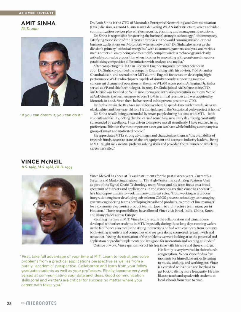
38
ALUMNI UPDATE
AMIT SINHAPh.D. 2001
"If you can dream it, you can do it."
Dr. Amit Sinha is the CTO of Motorola’s Enterprise Networking and Communication (ENC) division, a $200M business unit delivering WLAN infrastructure, voice and video communication devices plus wireless security, planning and management solutions.
Dr. Sinha is responsible for steering the business’ strategic technology: “It is immensely satisfying to see some of the largest enterprises in the world running mission-critical business applications on [Motorola’s] wireless networks.” Dr. Sinha also serves as the division’s primary “technical evangelist” with customers, partners, analysts, and various media outlets: “I enjoy being able to simplify complex wireless technology and clearly articulate our value proposition when it comes to resonating with a customer’s needs or establishing competitive differentiation with analysts and media.”
After completing his Ph.D. in Electrical Engineering and Computer Science in 2001, Dr. Sinha co-founded the company Engim along with his advisor, Prof. Anantha Chandrakasan, and several other MIT alumni. Engim’s focus was on developing high-performance Wi-Fi radio chipsets capable of simultaneously supporting multiple concurrent channels of operation on the same WLAN access point. At Engim, Dr. Sinha served as VP and chief technologist. In 2005, Dr. Sinha joined AirDefense as its CTO. AirDefense was focused on Wi-Fi monitoring and intrusion prevention solutions. While at AirDefense, the business grew to over $30M in annual revenues and was acquired by Motorola in 2008. Since then, he has served in his present position as CTO.
Dr. Sinha lives in the Bay Area in California where he spends time with his wife, six-year-old daughter and four-year-old son. He also indulges in the “occasional geeky project at home.”
Dr. Sinha recalls being surrounded by smart people during his time with MTL—both students and faculty, noting that he learned something new every day. “Being constantly surrounded by excellence, I was driven to improve myself relentlessly. I have realized in my professional life that the most important asset you can have while building a company is a group of smart and motivated people.”
He appreciates MTL’s strong advantages and characterizes them as “the availability of research funds, access to state-of-the-art equipment and access to industry leaders... Being at MIT taught me essential problem solving skills and provided the tailwinds on which my career has sailed.”
VINCE McNEILB.S. 1985, M.S. 1988, Ph.D. 1994
"First, take full advantage of your time at MIT. Learn to look at and solve problems from a practical applications perspective as well as from a purely “academic” perspective. Collaborate and learn from your fellow graduate students as well as your professors. Finally, become very well versed at communicating your data and ideas. Good communication skills (oral and written) are critical for success no matter where your career path takes you."
Vince McNeil has been at Texas Instruments for the past sixteen years. Currently a Systems and Marketing Engineer in TI’s High-Performance Analog Business Unit as part of the Signal Chain Technology team, Vince and his team focus on a broad spectrum of markets and applications. In the sixteen years that Vince has been at TI, he’s had opportunities to work in many different roles, “from working as a process integration engineer developing sub-micron CMOS process technology to managing systems engineering teams developing broadband products, to product line manager for a consumer electronics product team in Japan, to architecture team manager in Houston.” Those responsibilities have allowed Vince visit Israel, India, China, Korea, and many places across Europe.
Recalling his time at MIT, Vince fondly recalls the collaboration and camaraderie developed with other students in MTL “especially during those long days running wafers in the fab!” Vince also recalls the strong interactions he had with engineers from industry, both visiting scientists and companies who we were doing sponsored research with and notes that, “seeing the translation of the problems we were looking at to the potential end-application or product implementation was good for motivation and keeping grounded.”
Outside of work, Vince spends most of his free time with his wife and three children. His family is very involved in their church congregation. When Vince finds a few moments for himself, he enjoys listening to music, cooking, and working out. Vince is a certified scuba diver, and he plans to get back to diving more frequently. He also likes to teach and speak with students at local schools from time to time.

39
ALUMNI UPDATE
MARK SHANE PENGS.M. 1999, Ph.D. 2003
“Be bold and passionate to explore your different interests. The world is evolving so quickly that one never knows exactly what will be needed next. Don’t be afraid of how things are perceived today because tomorrow is always a different picture. Fortune favors the brave and the prepared.”
Mark currently serves as Manager in the ASIC services department of TSMC R&D, Design Technology Platform and works to maximize the ROI for everything TSMC does. His experience has taught him an important lesson: “The world is definitely evolving and globalizing at an increasingly rapid pace. MIT was great as a microcosm of that, and I believe that is what its main value is. I felt lucky to be a part of that, and to have had that benefit.”
Mark worked at a wireless startup post-graduation for “three very educational years” doing state-of-the-art high-performance analog design. After the company folded, Mark went overseas to work at a Chinese company. He has been involved in many areas while working at TSMC, the latest being 3DIC with TSV.
Mark comments, “At MIT and MTL, I was immersed in an intelligent community that was really aimed at bettering everyone and pushing the entire body to be a leading, world class institute. Such an environment and concrete output is the envy of all.” On personal challenges while at MIT, Mark recalls “the tapeout and subsequent measurement of my testchip. This was the first 'real' design I ever did. Besides the actual circuit design and realization of an idea, I had to package and test it as well which required another host of skills. I remember the late nights of design, measurement, and validation; the tough moments of what seemed like religious conversion. It was such a growth experience.”
Mark has also been busy learning Chinese idioms and has taken a keen interest in interior design and architecture. “Asia has lots of great concepts, which differ vastly with western instincts. Extending on this, I also like to collect Chinese wood furniture, which is functional art.” Mark is also married with three children.
KEEP IN TOUCH!To send us notes, pictures, stories, updates, or any other good news, please contact us using the Alumni Updater form found on the MTL website!
http://www-mtl.mit.edu/alumni.html

40
ALUMNI UPDATE
GRADUATION June 4, 2010
The annual reception for MTL graduates was held in the Grier Room on Friday, June 4, 2010. Hosted by Debroah Hodges-Pabon, this event brought students together with family, friends, and faculty to say their good-byes and embark on new beginnings. (All photos / Paul McGrath, MTL)

Same name, new venue.
Microsystems Technology LaboratoriesMassachusetts Institute of Technology60 Vassar StreetBuilding 39, Room 321Cambridge, MA 02139
IN APPRECIATION OF OUR MICROSYSTEMS INDUSTRIAL GROUP MEMBER COMPANIES: