Embed Size (px)
Citation preview

Volume 5, Issue 2, 2010
Solutions for Improving Fab Efficiency and Productivity
VIRTUAL METROLOGYFOR PREDICTIVE MODELING
CASE STUDY:ALTIS SEMICONDUCTOR
PREDICTIVE MAINTENANCE:PLANNING FOR THE UNPLANNED
ETCH CHAMBER MATCHING
The Agile Factory: Keeping Pace with Sudden Market Shifts

ContentsA Letter from Charlie Pappis 1
Agile Manufacturing: Creating a High-Mix Fab that Responds Rapidly to Meet Customer Demand 2
Moving into the Predictive Space with Virtual Metrology 6
Advanced Automation in LED Manufacturing 10
Energy-Saving Abatement in LED Factories 11
Case Study: Altis Semiconductor 12
Predictive Maintenance: Planning for Unplanned Events 14
PECVD Vacuum Integrity Application Enhances Display Manufacturers’ Throughput and Yield 17
Building Blocks to Boost Solar Productivity 20
Etch Chamber Matching Using Applied E3 22
The Last Word: ISMI Manufacturing Week 25
PUBLISHER: Dana TribulaEmail: [email protected]
EDITOR IN CHIEF: Liz BairdEmail: [email protected]
CONTRIBUTING WRITER: David [email protected]
Nanochip Fab Solutions is published by Applied Materials, Inc.
© Copyright Applied Materials, Inc. 2010.
www appliedmaterials com
To receive extra copies of Nanochip Fab Solutions or to add colleagues to the mailing list, please email
the following information to: [email protected]
o Name o Title o Company o Business address
Nanochip Fab Solutions is now available in an environmentally friendly online version
Please send an email to [email protected]
to request online delivery.
All trademarks so designated or otherwise indicated as product names or services are trademarks of Applied Materials, Inc. in
the U.S. and other countries. All other product and service marks contained herein are trademarks of their respective owners.

N a n o c h i p F a b S o l u t i o n s | V o l u m e 5 , I s s u e 2 , 2 0 1 0 | 1
A Letter from Charlie PappisCrEATINg ThE AgILE FACTory
Staying competitive in a tumultuous market is difficult for any business, but it poses particular challenges for the semiconductor and adjacent industries, where demand cycles shift in months, not years. how do you run a mix of technologically complex products at world-class cycle times, control costs to preserve profitability—and then turn your fab on a dime when demand suddenly changes? It seems like you’d have to be able to predict the future.
The secret to adjusting manufacturing operations to anticipate changing market conditions doesn’t involve fortune tellers, crystal balls or tea leaves. It takes adherence to a well-established business principle: agility.
What is an agile factory, and how can you create one? In this issue of Nanochip Fab Solutions, we focus on the latest thinking in predictive and preventive strategies that can help you get ahead of the curve—whatever its direction—by implementing solutions that increase yields, cut costs and deliver competitive advantage. Although predictive technologies are still emerging and evolving, there are productive solutions being used in fabs today, with many more innovations on the horizon.
We examine how manufacturers like you are using predictive maintenance to improve tool uptime and help avoid the unplanned failures that impact fab productivity. And you also get a glimpse of the state-of-the-art and the near future of virtual metrology—the predictive modeling technology that will one day provide a virtual copy of your fab, letting you reduce scrap and improve throughput and yield by anticipating future factory operations.
you’ll also read about Altis Semiconductor, a French foundry whose Applied Performance Service™ agreement allows them to pay a portion of their service costs based on operational results instead of a fixed price for tool service. The agreement has been so successful in controlling costs that Altis has now extended it—and is incorporating our powerful remote diagnostics capabilities as well.
This issue of Nanochip also reflects the survey results we received from our readers last summer. you wanted more articles on semiconductor-adjacent industries such as solar, LED and display—and you got it! We have included stories on building blocks for solar manufacturing, new productivity solutions for LED production, and predictive software that helps reduce cost and improve output in display manufacturing.
Take a look at these pages, then take a look at your fab. For customers who move toward agile manufacturing, we predict better times ahead. No crystal ball required. n
CHARLIE PAPPISgroup Vice President
and general Manager,Applied global Services

| V o l u m e 5 , I s s u e 2 , 2 0 1 0 | N a n o c h i p F a b S o l u t i o n s2
A gile is a frequently discussed term in manufacturing today, but agile manufacturing means something very different than another popular term: lean manufacturing. While lean manufacturing typically focuses on producing more with less and being the low-cost supplier,
agile manufacturing means being as responsive as possible to the customer’s constantly changing needs. Some of the strategies and techniques emphasized in lean manufacturing, such as fast cycle times, also apply to agile manufacturing. However, simply copying the principles of lean manufacturing as a strategy for becoming agile is not a guarantee of success.
AGILE Manufacturing: Creating a High-Mix Fab that Responds Rapidly to Meet Customer Demand

N a n o c h i p F a b S o l u t i o n s | V o l u m e 5 , I s s u e 2 , 2 0 1 0 | 3
Conventional wisdom in the semiconductor industry says that the lowest-cost producer usually wins. To drive down wafer costs, many semiconductor companies focus on improving economies of scale by building mega-fabs with more than 100k wafer starts per month (wspm). Because very few semiconductor companies can afford to invest in these mega-fabs, they need to find other ways to differentiate themselves from competitors. One way is to go beyond competing only on costs and become an agile manufacturer.
To become truly agile, a factory must meet several criteria. First, it must be able to run a large variety of products and processes in order to meet broad customer demand, and it must do this at world-class cycle times and competitive wafer costs. Simply running a wide variety of products is not sufficient; the fab must provide wafers at cycle times and costs that are comparable to traditional fabs, which in many cases are running closer to the traditional low-mix, high-volume paradigm.
An agile factory must also be able to respond quickly to changes in the product mix and volumes sought by customers. Again, having fast cycle times is critical to being responsive, as the fab throughput time will dictate how quickly an old or suddenly obsolete product can be replaced with new products that are in demand.
Finally, an agile factory must run with very high line yields. Given the large range of products, manufacturers with high-mix fabs cannot afford to run backup or extra lots to compensate for random scrap or yield issues—it is simply too expensive. Lots that are started must have a very high probability (>99.5%) of running through the entire line in order to ensure on-time delivery.
To meet these criteria, manufacturers must use advanced manu-facturing systems. Some of the systems are fab-wide, such as those for production control and global dispatching, tool control and pro-cess control, and capacity planning and equipment selection. Other systems are unique to the areas and tools most impacted by the high product mix, such as the lithography area, implant, metrology and inspection tools.
To achieve world-class cycle times, manufacturers must manage equipment constraints and reduce the sources of variability impact-ing the wafer flow in the fab. The relative impact of focusing on tool capacity and lot arrival variability can be judged through the use of the tool operating curve (Figure 1). The tool operating curve shows the relationship between lot queue time, or cycle time, and tool utilization. Two observations from the operating curve are especially relevant to this discussion. The first is that the cycle time increases very rapidly at
AGILE Manufacturing: Creating a High-Mix Fab that Responds Rapidly to Meet Customer Demand
Lot
Que
ue T
ime
Tool Utilization0% 10% 20% 30% 40% 50% 60% 70% 80% 90% 100%
FIGURE 1 ▲ Tool operating curve.

| V o l u m e 5 , I s s u e 2 , 2 0 1 0 | N a n o c h i p F a b S o l u t i o n s4
utilizations above 70%. As a result, at high utilizations reducing vari-ability in things such as equipment uptime, wafer processing time, and wafer arrival times can have just as great of an impact on reducing cycle time as increasing capacity. The theory and math behind the curve is beyond the scope of this article, but the message is simple: cycle time increases as tool utilization increases with the rate of increase at high utilizations determined by the amount of variability in the system.
One of the key tactics for reducing variability across the fab is to employ global dispatching or scheduling policies for all tools in the factory. Many manufacturers have found that employing fab-wide dispatching rules or policies to balance the flow of material through the line or to optimize the flow of material to the constraint tools can lead to dramatically higher throughput and lower cycle times with minimal capital expenditures.
In addition to using global rules to smooth the flow of lots through the fab, manufacturers are using customized rules at a few key tools that are most impacted by the product mix. These tools include the photolithography cells (track plus stepper or scanner), implanters, diffusion furnaces and associated wet benches. They are often referred to as having sequence-dependent run rates because the order in which lots are run on these tools dramatically influence their output. Consequently, these tools require dispatch rules that take this
dependence into account and create run plans that sequence lots to ensure the tools can support the factory starts.
The second observation is that at high tool utilizations, cycle time can be reduced significantly (25% or more) by increasing tool capacity by 5% -10%. This is due to the non-linear nature of the tool operating curve at utilizations greater than 70%, which was mentioned previously. While improving tool capacity by 10% can seem like a very challenging target, if the user approaches it from a holistic standpoint and focuses on a comprehensive metric like overall equipment effectiveness (OEE), it is possible to increase the effective capacity by focusing on both tool uptime and other areas. Examples of these improvement activities include decreasing scrap or rework, optimizing tool configurations and recipes, and improving wafer handling within the tool.
Many of the improvement techniques discussed require minimal expenditures or outlays—certainly much less than the capital cost of purchasing one or more new tools. As such, investments in infrastruc-ture and systems that help continuously reduce variability and increase capacity often provide very high returns on investment (ROI).
So what does this look like on the fab floor? A key tool set in any semiconductor fab is the lithography scanner and linked track. Given the large price tags for these tools—frequently $40 million or
Agile Manufacturing Challenges
running low-volume products with minimal scrap and at competitive costs
Supporting a large number of new products without disrupting production commits
responding quickly to shifts in product mix
Ensuring quality without inspecting every production lot
Flexing costs with loadings
Agile Manufacturing Strategies
Employing fab-wide dispatching and also scheduling in bottleneck areas like photolithography
Continuously improving bottleneck tool oEE
Utilizing cluster tools instead of batch processing tools
Employing advanced process control (APC) systems including r2r and FDC
Implementing cost structures that flex with loadings and fab utilization
TABLE 1 ▲ Agile Manufacturing Challenges and Strategies

N a n o c h i p F a b S o l u t i o n s | V o l u m e 5 , I s s u e 2 , 2 0 1 0 | 5
Author: Chris Keith. For additional information, please contact [email protected].
more—manufacturers try to maximize their output. As it turns out, these tools are also critical for agile manufacturing because they are one of the key pieces of equipment for differentiating products and enabling a high mix of products to be run in the same fab.
Agile manufacturers are extremely focused on their litho scanners and use several techniques to run these tools at high throughput with a large mix of products. First, they minimize changeover times by minimizing the number of photoresists plumbed to the same tool, reducing the resulting hot plate or oven temperature ramp ups and ramp downs that can temporarily idle wafer movement through the track. Their operations team focuses on creating batches of similar products that can be run through the tool together. They implement lot dispatching rules at upstream operations to create batches of similar lots that are fed to the litho scanner. They also use complex dispatching rules and sometimes short-interval scheduling at the lithography step to create batches of similar products that use the same reticle or that use similar track recipes.
Fabs with a small number of products frequently use product-based in-line monitors to detect process and tool excursions and
to maintain the high line yield required. Because of their low-mix, high-volume fab environments, these manufacturers can employ sophisticated sampling plans to simultaneously balance the risk of not quickly detecting a meaningful excursion or shift versus the additional capital required to purchase incremental metrology and inspection tools.
Agile manufacturers with a high mix of products cannot rely on direct inspection of product wafers as their primary in-line yield detection system because they would have to inspect almost every lot after every process step and purchase a very large number of inspection and metrology tools. Instead, they monitor and control the process tools themselves in order to detect and minimize excursions or shifts that might impact yield or reliability. Several systems are used to do this, including advanced process control (APC) systems such as run-to-run (R2R) control, fault detection and classification (FDC), tool and chamber matching, and advanced data mining for developing predictive models, including virtual metrology (VM). Another strategy that semiconductor companies–especially foundries–use to run a large number of products without a significant metrology burden is to provide a predefined set of devices, or cells, and rules that customers must typically use when designing their products.
Agile manufacturers make capacity and equipment selection decisions that are heavily influenced by the high mix of products they expect to run. They plan on having adequate buffer capacity when making decisions about how many tools to purchase. The buffer capacity makes it easier to change the product mix and loadings to meet shifts in customer demand. The additional buffer capacity is not required for all tool sets, but only for the tools discussed earlier that are more sensitive to product mix, such as lithography and implant.
Agile manufacturers also employ more cluster tools, which se-quentially process one wafer at a time, than batch processing tools, which process up to six lots in parallel using the same recipe. Cluster tools are preferred because of the high mix of products and recipes being run through the fab. In a high-mix environment, batch tools typically have much longer cycle times associated with waiting for a significant number of lots to queue up and run together.
Due to the cyclical nature of the semiconductor business, there are periods of time when demand and loadings will be significantly below the stated capacity of the factory. The manufacturer must be able to respond quickly by either finding new sources of demand or reducing fixed costs. As part of the trend to reduce fixed costs as a percentage of total costs, many manufacturers are outsourcing what were once considered core functions, including equipment maintenance and information technology (IT) and automation support.
In summary, being an agile manufacturer is all about being responsive. Fabs must be able to respond quickly to shifts in cus-tomer demand, both in total volume and mix, while maintaining competitive cycle times and cost structures. n

| V o l u m e 5 , I s s u e 2 , 2 0 1 0 | N a n o c h i p F a b S o l u t i o n s6
Virtual metrology (VM) is a new technology rapidly gaining ac-ceptance in the marketplace as an efficient and cost-effective way to optimize metrology value. It is less costly than conventional metrology, provides information much faster, and can work in tandem with conventional metrology to enhance the overall metrology performance.
VM is a modeling and metrology prediction solution whereby process and product data, such as in situ fault detection (FD) informa-
Metrology plays a crucial role in manufacturing. However, given its high capital equipment cost and cycle time impact on critical processes, metrology is a high-cost, high-stakes proposition. Further, issues with performance of metrology systems can lead to additional manufacturing cost and waste. These issues
include lack of ability to support wafer-to-wafer metrology, delays in metrology data feedback, and lost productivity from non-optimal process control and lack of optimized metrology strategies.
Moving into the Predictive Space with Virtual Metrology
tion and upstream metrology information is correlated to post-process metrology data. This same data can then be used to predict metrol-ogy information when conventional metrology data is not available. And a conventional metrology system augmented with VM can provide significant benefits (see Table 1). Indeed, the International Technology Roadmap for Semiconductors (ITRS) identifies VM as an increasingly critical technology for improving productivity and reducing waste (1).

N a n o c h i p F a b S o l u t i o n s | V o l u m e 5 , I s s u e 2 , 2 0 1 0 | 7
Benefit Approach
▲ Reduced cost of metrology (capital and cycle time costs)
n replacing portion of metrology with VM (reduce capital cost)
n “Smart Metrology”: utilizing VM to determine when actual metrology is needed (reduce cycle time cost)
▲ Improved product quality and yield
▲ Improved run-to-run (R2R) control process capability
▲ Reduced R2R control process variability
n Augmenting existing metrology (filling in the “gaps” due to no metrology measurement or delay)
n Incorporating virtual metrology data into r2r control schemes for move to full feed-forward/back wafer-to-wafer control
n Utilizing virtual metrology techniques for yield prediction
▲ Reduced product waste and equipment downtimen Utilizing VM data in fault detection schemes
n Utilizing VM to reduce need for non-product wafers
▲ Predictive maintenance
▲ Rapid maintenance qualification
n Using VM to better determine when equipment maintenance is needed
n Determining quality of maintenance operation through VM prediction of product quality
n Using VM to more rapidly determine when tools are qualified for production after maintenance
TABLE 1 ▲ Benefits achievable with virtual metrology and the approach taken with existing metrology and other factory systems to achieve these benefits.
hoW DoES VM Work?VM is an advanced software solution that utilizes process and product information, normally collected through fault detec-tion applied to a process, to analyze and predict product quality information. Historical fault detection, process, and metrology information is first collected for a given process in order to sup-port model development. If resources are available, design of experiments (DOE) data can also be used to facilitate this model discovery process. The information is used to develop base VM models leveraging techniques such as partial least squares-project on latent structures (PLS).
Trace data can be used instead of, or in addition to, fault detection information to support PLS modeling; however, based on Applied Materials’ experience, the complexities of model maintenance dur-ing run-time make the use of trace data on a run-to-run (R2R) basis somewhat impractical. Reduced data from FD models is sufficient to support high quality prediction models.
The base prediction models produced by PLS modeling are non-adaptive. In order for these VM base models to be effective we must add an adaptability capability—in other words, the models must be able to adapt to the dynamics, such as drifts and shifts, that are typically found in semiconductor processes. Many methods have been proposed for addressing these issues. Applied Materials has found that different methods are best suited to adapting to different dynamics. As a result, Applied has developed a unique adaptive VM capability. It includes a methodology that allows the VM system to “switch” between adaptation methods based on the process dynamics, thus providing significantly better prediction capabilities.
As an example of a practical VM application, Figure 1 shows sample results of a pilot study with Micron Technology, applying VM modeling to six chambers of a CVD process(2). The metrology values for each chamber were predicted with a high degree of accuracy using VM models derived from process FD data. Further, the adaptive VM approach was shown to be an improvement over non-adaptive VM.

| V o l u m e 5 , I s s u e 2 , 2 0 1 0 | N a n o c h i p F a b S o l u t i o n s8
FIGURE 1 ▲ Results from a virtual metrology pilot project with Micron Technology. The top graphs illustrate the ability of VM to model two chambers. The bottom graphs illustrate that adaptive virtual metrology (right) can better track process dynamics (in this case a process shift) than non-adaptive virtual metrology (left). The noise in the data just after the process shift near wafer 110 illustrates the need for methodology that allows the VM system to switch between adaptation methods (a single adaptation method was used in this pilot study).
Oxi
de
Thi
ckne
ssWafer Number
0 100 200 300 400 500 600 700 800 900 1000-15
-10
-5
tgt
+5
R2=0.71 Actual MetrologyPredicted Metrology
CHAMBER 5
Oxi
de
Thi
ckne
ss
Wafer Number0 100 200 300 400 500 600 700
-15
-10
-5
tgt
+5
R2=0.84 Actual Oxide ThicknessPredicted Oxide Thickness
CHAMBER 4
Oxi
de
Thi
ckne
ss
Wafer Number0 50 300100 150 200 250 350 400 450
-15
-10
-5
+5
tgt
+15
+10
Actual MetrologyPredicted Metrology
CHAMBER 5 – Adaptive PLS
Oxi
de
Thi
ckne
ss
Wafer Number0 50 100 150 200 250 300 450400350
-15
-10
-5
tgt
+10
+5
Actual MetrologyPredicted Metrology
CHAMBER 5 – Non-adaptive PLS
Oxi
de
Thi
ckne
ss
Wafer Number0 100 200 300 400 500 600 700 800 900 1000
-15
-10
-5
tgt
+5
R2=0.71 Actual MetrologyPredicted Metrology
CHAMBER 5
Oxi
de
Thi
ckne
ss
Wafer Number0 100 200 300 400 500 600 700
-15
-10
-5
tgt
+5
R2=0.84 Actual Oxide ThicknessPredicted Oxide Thickness
CHAMBER 4
Oxi
de
Thi
ckne
ss
Wafer Number0 50 300100 150 200 250 350 400 450
-15
-10
-5
+5
tgt
+15
+10
Actual MetrologyPredicted Metrology
CHAMBER 5 – Adaptive PLS
Oxi
de
Thi
ckne
ss
Wafer Number0 50 100 150 200 250 300 450400350
-15
-10
-5
tgt
+10
+5
Actual MetrologyPredicted Metrology
CHAMBER 5 – Non-adaptive PLS

N a n o c h i p F a b S o l u t i o n s | V o l u m e 5 , I s s u e 2 , 2 0 1 0 | 9
FIGURE 2 ▲ Vision of virtual metrology within E3 illustrating integration with FD and R2R components.
Author: James Moyne. For additional information, please contact [email protected].
Client Handler Application Adapter Discovery Manager
Oracle® Database
Data Access Layer
Data ServiceProvider
LogServer
StrategyEngine
VMBLOCKS
EPTBLOCKS
R2RBLOCKS
FDBLOCKS
GENERALBLOCKS
Applied E3™
INTEgrATINg VM WIThIN A FAB AUToMATIoN SySTEMWhile VM can clearly reduce cost and improve productivity, obtaining high ROI from VM implementations requires full in-tegration within a fab automation system so that the technology is reconfigurable and reusable. Since VM uses FD information to provide predictions, and since R2R control is one of the major consumers of VM information, the fab advanced process control (APC) automation infrastructure is the logical place to incorporate a flexible VM capability.
Applied E3™ is an APC automation solution that provides both FD and R2R control capabilities on the same SEMI E133 standard compatible platform. Thus, E3 is ideally suited to provide a VM capability (see Figure 2). VM “blocks” would just be another module provided in the E3 suite of capabilities alongside FD and R2R control modules. The VM blocks take FD output information from FD module “strategies” to make predictions. These blocks allow the user to select VM parameters to customize solutions and provide an adaptive VM capability that includes automatic switching between adaptation methods depending on process dynamics detected. VM strategies then dictate how the VM predictions are used (for example, export to R2R control strategies). The flexibility of the E3 strategy en-vironment allows the user to harness VM to realize the benefits listed in Table 1.
LookINg AhEADApplied Materials foresees a general movement from reactive to predictive operations in all manufacturing arenas. Fault detection will be replaced with fault prediction to further reduce scrap and equipment downtime. Predictive maintenance will augment preven-tative maintenance to further reduce downtime. Ultimately a fusion of real and virtual environments will take place, creating a virtual “copy” of the factory that operates alongside the real factory. The virtual factory models will be continually updated with real data and used to predict all aspects of future factory operations, reducing downtime and scrap, and improving throughput and yield. Virtual metrology technologies, along with other prediction capabilities such as scheduling and maintenance prediction, represent the critical first step toward a comprehensive predictive roadmap that we believe will inevitably lower costs and raise productivity for manufacturers of semiconductor, flat panel display and solar products. n
rEFErENCES(1) International Technology Roadmap for Semiconductors, (2010), www.itrs.net.
(2) k. olson and J. Moyne, “Adaptive Virtual Metrology Applied to a CVD Process,”
Proceedings of the 21st Annual SEMI/IEEE Advanced Semiconductor Manufacturing
Conference (ASMC), San Francisco, (July 2010).

| V o l u m e 5 , I s s u e 2 , 2 0 1 0 | N a n o c h i p F a b S o l u t i o n s1 0
Today, process engineers can take advantage of software that not only monitors their critical tools to improve throughput and quality, but can provide excellent correlation between tool performance and end product performance (Figure 1).
For improved throughput and bin yield, four things are required for effective manufacturing control in an LED facility:
A manufacturing execution system (MES) that tracks orders, work n
in process, recipes, lots, locations, times, etc. in real time.
Real-time process data from key tools that is captured in a database n
(reactor temperature, gas pressure, pump voltage, etc.).
Real-time measurement data from all of the metrology tools (in n
situ, probe, defect tracking, etc.).
A software system that can consolidate the data and perform n
real-time data analysis, plus automatically react to anomalies and process shifts. Today, many data management systems re-quire up to a week of compilation and analysis and still require engineering intervention.
Currently, there is little or no product tracking in many LED factories, including a lack of in-line measurement in the front- end process flow. Without the ability to understand the myriad correlations between critical front-end tool performance and the rest of the
As the fast-growing LED industry strives to achieve higher volume, manufacturers are starting to understand and realize the value of a software solution that can trace a product from wafer-to-die, to die-on-tape, and then to final product.
FIGURE 1 ▲ The powerful combination of automated process and metrology data, plus MES analytical capabilities, can result in more actionable information.
Real TimeProcess
Data
Real TimeMetrology
Data
MESData
AutomatingActionable
Improvement
TurningData into
Information
Advanced Automation in LED Manufacturing

N a n o c h i p F a b S o l u t i o n s | V o l u m e 5 , I s s u e 2 , 2 0 1 0 | 1 1
manufacturing process, it is challenging to improve quality, cost and control of bin size.
Applied E3™ software can take comprehensive manufacturing data and analyze it in a way that translates the data into actionable information. The E3 technology connects and analyzes vast amounts and types of data to create useable information, such as indicating the root cause of a problem in a way that enables action. Using process data, the E3 engine drives statistical control limits for the process and receives automatic notifications when limits are breached. Operators can easily compare process tools or chambers side by side to match the reactors to the performance of a “golden” chamber.
Author: Phil Walker. For additional information, please contact [email protected].
Applied iSyS™, an integrated sub-fab system from Applied Materials, is built around an innovative mainframe and is ideally suited to high throughput LED manufacturing, matching critical vacuum pumps and abatement technologies to the specific application challenges of MoCVD processing. iSyS systemizes the LED subfab, demonstrating that synchronization of discrete subfab components and integration with process tool interfaces can deliver >30% energy and carbon equivalence reduction. The smart idle interface modulates vacuum pump and abatement operation, matching the dynamic process demands of LED manufacturing to reduce cost per device. hydrogen, ammonia and chlorine are present in the MoCVD process chamber exhaust. Therefore, it is critical that the entire exhaust gas path—from the chamber to abatement—is heated to avoid ammonium chloride deposition, and that interconnection pipelines are short to conserve energy. iSyS incorporates insulation, contact heating and constant monitoring to safely handle exhausts and ensure maximum uptime and minimum maintenance. Consideration of the abatement challenges for ammonia and chlorine are also critical to environmental compliance. Further, careful selection of the abatement technology is important in meeting customer specifications for Nox, water nitrates, and water hardness. For LED manufacturing, iSyS has been configured and installed with effective water CaCo3 hardness management through interactive ph control, nitrate and nitrite wastewater management through combustion control, and Nox control through process tool synchronization.
In LED production, the high flow pumping of process gases at low chamber pressures (approaching 5-10 Torr) is crucial. The low molecular weight and viscosity of hydrogen can result in leakage between compression stages of vacuum pumps, requiring more pumping energy to maintain low chamber pressure, which if deficient, can impact production throughput and quality. The selection of subfab components such as pumps, abatement, chillers and so forth, is critical to achieve optimum energy and process efficiency, so Applied Materials pre-qualifies and partners with leading suppliers to provide process specific component options. For instance, working with strategic partners, Applied Materials has demonstrated a new energy saving pump technology for iSyS LED subfab systems that can achieve up to a 40% improvement in dynamic pump rotational energy over conventional vacuum pumps. In 2010, the innovation of iSyS technology was recognized with the prestigious EuroAsia IC Industry Subsystems & Components Award, and iSyS was named the Sustainable Technology of the year by Semiconductor Equipment and Materials International (SEMI). As the volume of LED production continues to rise, solutions like the integrated iSyS subfab system offer manufacturers the opportunity to efficiently scale their business while achieving their sustainability targets and lowering their operating costs. n
Energy-Saving Abatement in LED Factories Sustainable energy-saving manufacturing processes are as great a priority for LED manufacturers as they are in semiconductor and related industries. The metal organic chemical vapor deposition (MOCVD) technology used in LED production presents significant environmental, health and safety compliance issues and high energy costs that can impact the bottom line.
The E3 technology, coupled with Applied’s SmartFactory™ MES, provides a complete solution for correlating tool performance to actual product final binning. This critical insight into the complete process is key to delivering the highest yield on the most important and highest margin parts. With this technology, the next level of process tuning is finally available to LED producers to ensure a holistic approach to improving the manufacturing process. n
Advanced Automation in LED Manufacturing
Authors: Phil Chandler and Daniel Clark. For additional information, please contact [email protected].

| V o l u m e 5 , I s s u e 2 , 2 0 1 0 | N a n o c h i p F a b S o l u t i o n s1 2
The impetus for the APS agreement was to improve Altis’ ability to adapt to the demand cycles of the semiconductor business. “We know how the market runs, with upturns and downturns impacting all manufacturers. When in a downturn, the APS agreement helps us control our costs,” said Nicolas Miannay, chief operating officer at Altis. The APS program paces service and price to actual utilization rates. This provides committed uptime performance at a low, predictable cost that tracks with factory loading.
The agreement was initiated four years ago as Altis was ramp-ing its copper interconnect technology. With PVD being key to its copper process, Altis first included contract provisions aimed at improving the uptime of its Applied PVD tools. Together, Altis and Applied examined data tool set by tool set to arrive at mutually agreed improvement goals. Eventually, the APS agreement was expanded to cover more than 40 Applied tools, including etch and CVD systems, at the Altis facility. “With the variable cost model, we no longer pay for field support activities; we pay for operational results. This is a fundamentally different way of approaching main-tenance in our fab,” said Miannay.
One strategy for navigating the cyclicality of the semiconductor market is to employ a variable cost model for equipment
maintenance services. This approach allows manufacturers to align their service costs to fab production, so a portion
of their service costs are based on tool output, not just fixed tool service fees. The flexibility to adjust support services
to match tool utilization has certainly helped manage costs at Altis Semiconductor, a French foundry operation that signed its first
Applied Performance Service (APS) agreement with Applied Materials in 2006, and renewed and expanded its contract this year.
APS is an innovative tool maintenance program that ensures excellent tool performance with a com-mitted uptime, plus a billing structure that allows tool
maintenance cost to flex with production rates. APS customers receive 7x24 support for service and parts, including all corrective and preventive maintenance and wet cleans. An APS agreement involves a negotiated fixed monthly fee and a variable fee that is based on a tool-specific output measurement. Etch tools, for example, are billed based on RF minutes used. The uniquely flex-ible APS program can reduce maintenance costs by an average of 15%, making it a particularly powerful strategy especially in times of rapidly changing demand.
Jean-Marc Pinvidic, Altis maintenance manager, noted that for some tool sets, the company has achieved a 10% uptime improvement. “That demonstrates the value of collaboration and the value that Applied brings. The key is to establish strong communications and ensure that both parties are fully aligned with the best plan to drive manufacturing improvements,” he said. The expanded APS agreement now involves daily meetings between Altis maintenance engineers and the on-site Applied technicians and managers to ensure open communications.
| V o l u m e 5 , I s s u e 2 , 2 0 1 0 | N a n o c h i p F a b S o l u t i o n s 1 2
CASE STUDY
Altis Semiconductor— Predictable Costs for Fab Services

N a n o c h i p F a b S o l u t i o n s | V o l u m e 5 , I s s u e 2 , 2 0 1 0 | 1 3N a n o c h i p F a b S o l u t i o n s | V o l u m e 5 , I s s u e 2 , 2 0 1 0 | 1 3
Authors: David Lammers and Nanochip Staff. For additional information, please contact [email protected].
As part of a strategy to further improve productivity and reduce costs, the two companies are working together on programs to enhance predictive maintenance techniques, including deploy-ment of Applied ExpertConnect™ remote diagnostics capability. ExpertConnect enables highly secure remote diagnostics and rapid resolution of complex equipment downs by engaging Applied’s team of experts and best practices at the local, regional and global levels. In addition to improving overall maintenance efficiency and reducing costly downtime, ExpertConnect also provides monitoring systems that support predictive maintenance.
The predictive approach helps prevent unplanned downtime by monitoring feedback from tool sensors. This sensor data is used to identify failing parts before they impact wafer quality or cause the tool to fail. It can also extend the useful life of critical parts based on cumulative data.
“We are talking with Applied now about various approaches to predictive maintenance, seeking a better understanding of perfor-mance of our chambers,” said Pinvidic. “We are working together to optimize tool sensor limits that maximize tool uptime and part life, while minimizing unplanned downtime. It is a key cost reduction opportunity for us.”
With support levels matching to fab loading and customer de-mands, Miannay said the APS agreement has allowed Altis to adapt. “We can match the needs for support to the level of fab loading and the demands of our customers. What we look forward to in the next year or so is even greater flexibility and the opportunity to expand this support approach to different categories of tool sets as we continue to develop new technology options.”
Beyond flexibility and improved uptime, the APS agreement helps Altis reduce fixed costs for maintenance infrastructure. Miannay added, “Overall, the Applied Performance Service is enabling us to achieve world-class tool performance with predictable cost.” n
Altis Semiconductor Now A Foundry Operation After an eight-year period making DRAMs for IBM and Siemens/Infineon, and then a decade manufacturing various logic components for its two parent companies, Altis has entered a new phase. Altis Semiconductor (Corbeil Essonnes, France) became a European-based specialty foundry in August of this year. Operating at a 135-acre site south of Paris, complete with a design center and 20,000 square meter cleanroom, the company is focused on bringing innovative manufacturing solutions to a wide range of customers.
“our real strength is that we have had many opportunities to address many different markets, requiring new technology offerings. We have a technology portfolio which address a lot of different market segments,” said Nicolas Miannay, the chief operating officer at Altis.
one such technology is 0.13micron logic with copper intercon-nects. Altis was very early—in fact, the first in Europe—to have a copper capability, starting at the 0.18 micron node and then quickly introducing copper at the 0.13 micron node.
“With our copper logic capability, we have the ability to address a range of markets, and we will continue to do so,” he said. “A lot of other specialty foundries, which we contrast with the ‘pure-play’ foundries such as TSMC, gLoBALFoUNDrIES, and UMC, still do not offer copper interconnects,” Miannay added.
Besides copper logic, Altis’ technology offerings include rF, flash and other non-volatile memories, plus high-voltage options. Miannay notes that the success of Infineon’s rF products reflects well on Altis, which counts wireless among its served markets.
Altis will work with customers to develop new products and will have the flexibility to partner with its customers to address value-add products on niche applications. Miannay adds, “We have the ability to give them the attention required to bring their innovations to the marketplace. This is reflected in our daily way of thinking: customer as a first priority, innovation as our key success factor.” n
For more information, visit Altis at www.altissemiconductor.com.

| V o l u m e 5 , I s s u e 2 , 2 0 1 0 | N a n o c h i p F a b S o l u t i o n s1 4
Given the potential for significant savings from using predictive main-tenance, it is not surprising that leading players in the semiconductor industry have active programs underway. Sematech’s ISMI organiza-tion is conducting two pilot projects, where equipment and device
manufacturers are cooperating with leading university researchers. David Stark, ISMI e-Manufacturing project manager, said ISMI’s effort combines scheduled maintenance, decision modules, and predictive and non-predictive condition-based maintenance (CBM).
Predictive maintenance (PdM) is the ability to predict the future failure of a major part on a system before it impacts the quality of the end product. PdM is emerging as an immensely important and powerful method to improve tool uptime and avoid the unplanned failures that can cripple a fab’s productivity and yield. “A lot of
people don’t grasp the totality of predictive maintenance and how it can impact a facility,” said Mark Boone, program manager at Texas Instruments’ 300mm DFAB in Dallas. “Semiconductor production equipment is extremely complex. A large fab can have 800 to 1,000 tools, and despite significant improvements in tool reliability, equipment fails are the primary disruptor in a typical fab.”
Predictive Maintenance: Planning for Unplanned Events

N a n o c h i p F a b S o l u t i o n s | V o l u m e 5 , I s s u e 2 , 2 0 1 0 | 1 5
The predictive CBM module reports on the remaining useful life of the tools or critical parts.
The predictive module, Stark explained, encompasses sensor data, trace data, counters, virtual sensors, in-line metrology and alarms. These inputs are monitored and compared against known “pre-failure” signatures by diagnostic applications. When one of these signatures is identified, a maintenance action can be planned to correct the problem. This prevents potential wafer loss and avoids unplanned system downtime. Other benefits include longer life for critical parts, an extension of scheduled maintenance cycles, and reduced diagnosis and repair time. Yields may also improve when critical work in process (WIP) is sent to the equipment that is performing best.
The pilots being conducted at fabs run by two of the ISMI consortium members have demonstrated longer maintenance cycles for chamber cleaning, extended lifetime on electrostatic chucks and improvements in diagnostics.
TACkLINg UNPLANNED DoWN TIMEFor Applied Materials, PdM is seen as a key weapon in the battle against unplanned down time (UDT). Jerry Gross, director of global product support at Applied Global Services (AGS), said, “Our customers tell us the most costly maintenance event is an unplanned down. It can disrupt the balance of the whole line with impact far beyond the down tool.”
The goal of PdM is converting an unplanned event to a planned event. “If we can schedule the replacement of a part during planned preventive maintenance, the tool is only taken down once instead of twice, and the risk of wafer scrap is greatly reduced. That’s a significant benefit to the customer.”
The other major payoff is getting the most out of critical–and often costly–equipment components and parts. Normally, custom-ers replace such components on a regular schedule to avoid the risk of yield-killing part failure during system operation. However, if customers had mechanisms to assess part condition in situ, they could potentially extend the useful life of the component. Manjunath Yedatore, service technology program manager for AGS, estimated that one Applied customer saved more than one million dollars a year when analysis revealed that the electrostatic chucks on their Applied tools could be safely kept in operation much longer than originally expected.
“Using sensors and simulation algorithms, we were able to show—based on data from characterized failures—that the parts on their systems had a much longer useful life than first expected,” he said. “Looking at the before and after data in this customer’s operation, we concluded that the electrostatic chuck was performing to spec well beyond the timeframe in which they would normally have replaced it.” Yedatore stressed, however, that it is impossible to generalize. Not all parts in a particular tool type will deliver the same performance. Much depends on the process and production protocols of each tool. For example, since the basic physics of electrostatic chuck operation
is very similar, the learning from one characterization will greatly expedite rollout and implementation of electrostatic chuck predictive maintenance to other customer sites, other processes.
PdM technology relies on data from sensors. These range from electrical sensors measuring current, voltage and resistance, to others that record acoustic patterns, pressure, temperature, vibration and viscosity. To date, sensors have been used primarily for equipment development and troubleshooting, but are now becoming part of the mainstream production tool maintenance protocol with PdM.
For example, in the case of e-chucks, vibration sensors monitor the mechanism which lifts the wafer into place. As the pins in the mechanism start to wear out, the assembly begins to chatter. The e-chuck must present the wafer to the robot at precisely the right moment. The slightest delay can result in a broken wafer. If the vibration sensors start to detect chatter on the lift mechanism, other data is collected, and all that information can be used to predict when the part will fail.
With PdM, Yedatore explained, “we’re now beginning to take sensor measurement to next level. The trick is to know what sensor information matters, and which sensors are relevant to that particular failure mode. We often have to look not just at one, but at two or three sensors.”
Applied’s PdM team is working internally with product develop-ment groups to incorporate on-board sensors dedicated to predictive maintenance in the core design of new production tools. Applied’s PdM team is applying the approach to a wide variety of parts, con-centrating primarily on parts with large impact to the results on the wafer. “We look at parts whose failure has the highest likelihood of wafer scrap,” Gross said. “These are the areas that the customer cares about the most.”

| V o l u m e 5 , I s s u e 2 , 2 0 1 0 | N a n o c h i p F a b S o l u t i o n s1 6
Gross said that PdM is beneficial in several ways. First, preventing an unplanned down not only minimizes wafer loss but also increases output since a planned down is always shorter than an unplanned down. When a customer is notified in advance that a part is going to fail, they don’t have to spend time troubleshooting, which saves many hours. Since it’s planned, replacement parts can be ready and waiting. Secondly, PdM can actually keep good parts in service longer by taking the guesswork out of knowing how long a part can be safely used. Finally, and most importantly, an unplanned down has the potential to interrupt wafer flow throughout the fab as well as risking wafer scrap for wafers in process when failure occurs. Minimizing scrap and variability is key to a factory’s productivity.
PDM DIAgNoSTICS TooLS Applied Materials Japan AGS product manager Takeshi-Kei Kawada said that in the 200mm era, Japan-based IDMs largely used in-house software to gather tool data. As they move to 300mm fabs, however, the major chip manufacturers are shifting to automation and remote diagnostics that help support PdM efforts. “Now, the leading technology customers ask us to predict future tool failures. We use Applied ExpertConnect™ remote diagnostics to collect and analyze equipment sensor data to see if the tools are running normally or abnormally.”
The combination of remote diagnostics and PdM saves time and money because Applied’s expert engineers can evaluate warn-ings and decide whether or not to deploy on-site service engineers. “Sometimes, our expert can just look via ExpertConnect and deter-mine that certain performance characteristics are normal for a given tool, in which case, the customer can continue to run production lots,” Kawada said.
Applied combines PdM models that are being developed with ExpertConnect and advanced process control techniques – all con-trolled by the Applied E3™ fab-wide automation and equipment engineering system (EES). This approach correlates data coming from the tool with the device characteristics. When the E3 system detects an anomaly in performance of a critical part it signals an alert that will trigger preventive maintenance on the tool. This helps the customer avoid extended downtimes and lengthy delays in shipping products to their customers.
At Texas Instruments, PdM techniques are mainly focused on preventing unplanned downtime for “constraint” fab tools—those which can create costly production bottlenecks. But TI is also applying PdM to its more expensive facilities equipment, such as chillers, air compressors, high-voltage electrical transformers and others. TI maintains backups for all of its key facilities equip-ment, something that is not practical for fab tools, according to Eric Whitmore, TI’s Texas-based facilities program manager. For chillers, the company uses oil and vibration analysis to monitor the health of its equipment. Infrared thermography is used to scan electrical equipment for hotspots, and ultrasonic technology is used to evaluate other components.
ThE BoTToM LINEGross said he views PdM as part of a key strategy to increase output and quality of the end product, as well as to reduce costs. “At every step of the production process, getting costs down is important to IC manufacturers, and maintenance is an important area of opportunity. Increasingly, we at Applied Materials are using PdM technologies as part of how we deliver service to our customers—minimizing the lost value of misprocessed wafers and the opportunity costs of unplanned downs are a priority for all of our customers.”
Applied’s strategy, Gross said, is to continuously develop predictive capabilities, adding data to its models, improving the sensor package on its tools, and refining the PdM algorithms, then building them into service products that deliver greater value to the customer. “We approach service differently,” Gross said. “Through innovative PdM techniques we expect to not only help improve system uptime, but to ensure that customers are getting optimum performance whenever the tools are running.”
Will predictive maintenance help the chip industry make UDT a thing of the past? PdM takes time to implement effectively, as each part has its own failure patterns. But as more resources are devoted to developing algorithms, models, and sensors, and as we derive more learning from PdM services, it’s clear that PdM will soon become an industry mainstay. n
Authors: David Lammers and Nanochip Staff. For additional information, please contact [email protected].

N a n o c h i p F a b S o l u t i o n s | V o l u m e 5 , I s s u e 2 , 2 0 1 0 | 1 7
Built on the Applied Materials’ industry-leading E3 equipment engineering system, the new E3 AKT PECVD Vacuum Integrity Application continuously monitors key system parameters. This lets fab operators detect and even predict vacuum compromises, then quickly react to correct the tool before these faults impact throughput and yield. With this critical capability, manufacturers can potentially reduce scrap for higher line yield, as well as dramatically reduce the unscheduled maintenance time needed to trace and correct vacuum excursions. The result is higher system uptime and throughput, and higher return on investment.
SoLVINg ThE VACUUM ChALLENgEEven though equipment engineers routinely perform sophisticated vacuum integrity checks on production tools before system startup or restart, degradation of vacuum between scheduled checks is difficult to detect—by the time the vacuum fault is causing scrap it is usually too late, because the film may be contaminated or compromised. Figure 1 shows how by continuously monitoring vacuum integrity and chamber pressure using E3 technology, customers can oper-ate with maximum process time while minimizing daily vacuum monitoring activity.
PECVD Vacuum Integrity Application Enhances Display Manufacturers’ Throughput and Yield
One of the key tools in flat panel display manufacturing, the PECVD system, depends on many factors to maintain operating vacuum. Vacuum leaks in PECVD equipment, while extremely uncommon, can be very costly and troublesome. Although relatively large vacuum leaks are typically detected by on-board
software, small leaks can be very difficult to detect and are usually detected only after a scrap event. Manufacturers have long sought a proactive capability that can detect leaks during processing, or even anticipate excursions before they become a problem.

| V o l u m e 5 , I s s u e 2 , 2 0 1 0 | N a n o c h i p F a b S o l u t i o n s1 8
As a specialized application engineered for the AKT PECVD systems, the Applied E3 AKT PECVD Vacuum Integrity App detects compromises in the vacuum system well before they can affect pro-cess output. Applied Materials’ familiarity with its production tools provides a distinct advantage in knowing what sensors to monitor to collect the appropriate process data, how to organize and display the collected data, and how to best act on the data.
The E3 AKT PECVD Vacuum Integrity application continuously monitors chamber pressure during the deposition process using a predefined univariate analysis (UVA) model (Figure 2). At any de-viation from normal operation, the application alerts engineers to the existence, or even the beginning, of a pressure abnormality in an AKT PECVD tool. This enables timely intervention before the pressure issue can impact product quality. Because the application minimizes the time required for regular maintenance, and dramatically reduces unscheduled maintenance for vacuum correction, customers have reported producing three or four more pieces of glass every day. One customer detected vacuum problems 4 hours faster than with their own internal monitoring system, improving tool uptime 1.5%
per year and reducing scrap over 95%; these translated to savings of $800,000 per year in scrap costs alone. Other customers have estimated cost savings of over $350,000 per month, based on reduced scrap and increased production output.
ProVEN PAThWAy To IMProVED VACUUM INTEgrITyAlready well proven in the display industry, the E3 App is a turnkey solution for AKT PECVD tools that offers tool-specific models for rapid setup and use. With its predefined UVA model designed specifi-cally for monitoring vacuum, the E3 app easily and automatically connects to the process data interface layer, which is called the IEDS software on AKT PECVD tools (Figure 3). Upon detecting a signal indicating a vacuum issue, including hard-to-find small pressure or atmospheric problems, the application triggers an alert to system engineers via email so they can take immediate action.
E3 oPErATIoNThe E3 AKT PECVD Vacuum Integrity App is based on continuous review of trace data from the CVD tool that correlate to vacuum in-tegrity issues in the process chamber. The UVA model monitors many different parameters, including multiple gas pressure differentials from a target setting. By comparing signals against a baseline signature, excursions are easily detected. The vacuum detection model initially checks for process chamber compromises by monitoring the pumping rate at the beginning of the process. The model identifies the specific pump, glass sheet, and other parameters to be tracked.
The application is very easy to use, even by relatively untrained operators. All process recipes can be monitored with a single UVA collection strategy. The configurable dashboard provides extensive tools for plotting real-time data, analyzing various data sources, and monitoring equipment health. Equipment engineers can drag and drop data into specific and relevant views, as well as access all tool data
FIGURE 1 ▲ The E3 AKT PECVD Vacuum Integrity App lets manufacturers gain process time by reducing time for routine leak checking by 50% or more.
Processing time
Regular leakcheck operation
Regular leakcheck operation
Regular leakcheck operation
Processing time Processing time
Processing time Processing time
FIGURE 2 ▲ This report shows chamber pressure pumpdown trace data over time. Blue and yellow lines represent the upper and lower limits for chamber signature analysis; there are 4 traces outside of the UVA signature envelope, possibly indicating that pumpdown time is slow or reacts late compared to a target response. The E3 AKT PECVD Vacuum Integrity App uses this data to notify users that the tool and process have degraded and require service.
Pre
ssur
e (k
Pa)
Time (secs)
00.00.00 00.00.15 00.00.30 00.00.45
100K
90K
70K
80K
50K
60K
30K
40K
10K
20K
0
Signature View for AKTCVD01/FastPump/Pressure

N a n o c h i p F a b S o l u t i o n s | V o l u m e 5 , I s s u e 2 , 2 0 1 0 | 1 9
Authors: Seong-Hoon Lee and Scott Bushman. For additional information, please contact [email protected] or [email protected].
as overlay collections and views. Using its modeling window, for example, engineers can use the visual information to make informed decisions based on data or sensor values. Engineers can then easily create context groups and custom algorithms, select data items (sensor values), and use different statistics on these data items.
Several components are included in the complete E3 AKT PECVD Vacuum Integrity App:
Software - The IEDS adaptern instantly connects the application to the AKT PECVD tool(s) and collects process, monitor, and event data from the tool and stores it in file format data form directly from the tool. The IEDS adapter directly retrieves the data from the system’s IEDS software, enabling instant analysis in the throughput improvement application.The E3 fault detection and classification (FDC) modulen is the software backbone for collecting and integrating tool data, such as sensor readings and events, into a common Oracle database. This enables other E3 modules to access this data. Knowledge - The AKT PECVD throughput improvement n
application contains the predefined UVA fault detection model that detects vacuum issues during the deposition process, in-cluding highly configurable fault and intervention levels. A configurable dashboard assists users in plotting and analyzing real-time data.
Integration/Deployment/Support/Hardware - n The E3 AKT PECVD Vacuum Integrity App includes user training as well as one full year of maintenance and support. Applied’s on-site E3 deployment teams can install preconfigured hardware systems quickly and provide a single point of contact for hardware and software components.
CoNCLUSIoNThe E3 Vacuum Integrity Application for AKT PECVD systems offers display manufacturers valuable, cost-effective protection from undetected vacuum issues, with the potential to dramatically elevate system throughput and fab line yield. This turnkey fault detection package includes tool integration, software implementa-tion of the preconfigured fault detection model, user training and one year of warranty maintenance. Applied Materials’ experienced deployment teams provide fast, on-site installation that can be up and running in a matter of hours, bringing many key economic benefits to fab operators. n
FIGURE 3 ▲ E3 Univariate Analysis (UVA) collection screen allows users to configure a UVA model for different process sensors, recipe step conditions, and different statistics and enables the user to adjust model sensitivity for individual process recipes.

| V o l u m e 5 , I s s u e 2 , 2 0 1 0 | N a n o c h i p F a b S o l u t i o n s2 0
To facilitate that growth, Applied Materials and its partners are working to address four interrelated building blocks to develop and meet the c-Si manufacturing roadmap: higher efficiency cells, advances in automation, higher throughputs for improved factory productivity and thinner wafers. These building blocks are key to further reducing cost per watt in c-Si solar.
As c-Si solar factories grow in size and sophistication, equip-ment and process innovations will be required to produce higher efficiency solar cells and to reliably handle cost-saving thin wafers on production lines that process several thousand wafers per hour. Automation techniques such as equipment performance monitor-ing and data mining, already widespread in the semiconductor and display industries, are now being adopted by a growing number of solar manufacturers who recognize the potential to boost factory output and reduce costs.
hIghEr EFFICIENCy CELLSWhile solar energy is largely cost competitive in terms of peak energy production, solar fabs must undergo another round of efficiency and throughput improvements to fully compete with the price of less clean forms of energy. To that end, the solar industry is working to create cells with taller, thinner conductors that minimize the shadowing effect (the amount of sunlight that is shaded from the solar cells below). Using ever-thinner wafers, several of the process steps involve conductor patterning on top of a prior pat-tern, using screen printing equipment that can align and register the position of the wafer without interrupting the process. The Applied
Baccini Esatto™ technology, for example, is capable of ±15 micron alignment accuracy in a double patterning process, increasing cell efficiency by 0.25%. The challenge is to meet these tight alignment specifications while also boosting wafer throughput.
As environmental scientists help raise global awareness of the urgent need for clean energy, engineers are working to expand production and improve the efficiency of crystalline silicon (c-Si) solar factories. “Application of solar to the electric power industry is evolving—it is becoming mainstream,” said Charlie
Gay, president of Applied Materials’ Solar Products group. “Five years ago, a 25 MW solar fab was a healthy size. Now, companies routinely plan 300 MW-scale fabs, and some are considering fabs on the scale of 3 GW over the next few years. And the goal is to produce solar cells at a cost of $1.00 per watt—or less,” he added.
Building Blocks to Boost Solar Productivity
Charlie Gay, ▲ President, Applied Solar Products Group

N a n o c h i p F a b S o l u t i o n s | V o l u m e 5 , I s s u e 2 , 2 0 1 0 | 2 1
Authors: David Lammers and Nanochip Staff. For additional information, please contact [email protected] or [email protected].
Further improvements in cell efficiency can be achieved through advances in paste optimization and screen printable dopants for selec-tive emitter and double printing applications. Applied is working on innovative cell structures that place all the contacts on the back surface of the wafer, eliminating the shadowing effect entirely.
AUToMATIoN, STEP By STEPMany solar factories today operate with little or no tool or factory software automation. Those that have automation on individual tools often use custom software, which is labor-intensive to create and expensive to maintain.
That presents a real opportunity for the solar industry to leverage well-known productivity methods. If the solar industry is to achieve its goal of a dollar-per-watt, the cost of each processing step must be reduced. This requires high productivity systems optimized for individual processes, combined with intelligent, affordable factory and process control software.
Applied Materials is developing a new generation of equipment which will offer process diagnostics, monitoring and control capability already built in. To help drive throughput improvements, Applied has also adapted its Applied E3™ equipment engineering system used in IC and display manufacturing to provide c-Si manufacturers with information on tool uptime, yields and process control.
Leveraging its expertise in the semiconductor industry, Applied is adapting a range of productivity tools including data mining, sophisticated process control, flexible scheduling and dispatching, as well as an entire manufacturing execution system: Applied Smart-Factory™. “We are making it possible for a factory manager to see in real time how well the facility is running—to run the business and fine tune it,” said Gay.
hIghEr ThroUghPUTSCompared to semiconductor fabs, wafers move more quickly through solar production lines and the wafers are much thinner, requiring sophisticated handling to minimize breakage. Gay noted that solar cell fabs use far fewer process steps than IC fabs, but the volume of material is much higher. “Pushing thin wafers through at very high speeds requires sophisticated technical solutions. Silicon is brittle and fragile,” he said. “For example, to move wafers at high speeds we need to use Bernoulli chucks and techniques that do not touch the wafer. To achieve higher throughputs, we want to be able to process continuously, but wafers need to stop for the application of a conductor pattern or similar steps.”
To boost throughput in wafering, the Applied HCT B5™ wire saw will incorporate innovations such as crimped wire to further increase sawing speed. The extendible Applied Baccini Soft Line™ screen printing platform can handle thin wafers at more than 1,440 cells per hour, and yields are further optimized with the factory automation software that Applied has introduced to solar fabs. Going forward, c-Si factories will achieve higher throughputs by integrating higher productivity equipment plat-
forms with modeling and statistical process control such as that found on E3.
ThINNEr (BUT NoT Too ThIN) WAFErS While the IC industry starts with wafers that are about 750 micrometers (microns) thick, the solar industry has been driving to thinner wafers in order to save on silicon, the largest material cost in solar cell pro-duction. Today a solar wafer is about 170 to 190 microns thick, about half the thickness of a decade ago. In the coming decade, the pace of innovation will result in wafers 80 microns thick, and eventually 40 microns. “ There is a limit to how thin solar wafers can become, determined by the need to absorb the majority of the sunlight striking the wafer,” Gay said. “It is possible to make a thinner wafer, but if you hold it up to the sun you would see porous light. It is really hard to absorb photons with anything thinner than 40 microns.”
A hIgh groWTh MArkETAs c-Si solar applications become more mainstream, innovation will come from very sophisticated suppliers such as DuPont, Hemlock and Heraeus Materials Technology LLC on the materials side, as well as established companies like Applied Materials on the equipment side. Applied’s plan, said Gay, “is to collaborate closely with leading wafer and materials suppliers, to build on the momentum in wafering and cell manufacturing, and to leverage advanced automation software platforms such as those offered by the company’s Applied Global Services business.”
Innovation is accelerating as the PV industry scales and as the solar industry borrows from lessons learned in semiconductor production. Noted Gay, “Solar fabs now annually produce cells and modules capable of making roughly 15 GW of electricity, and the entire industry generates revenues on the order of $60 billion. With clean energy on the agenda of societies everywhere, many of the largest chip-making companies are entering the solar field.” Taiwan Semiconductor Manufacturing Company, for example, re-cently acquired Taiwan-based module maker Motech Industries Inc. “These IC vendors know how to handle wafers and processes and have long histories of leveraging automation in their manufacturing lines,” he added.
In addition to gaining the attention of sophisticated equipment and materials suppliers, the solar industry is attracting talent from the semiconductor industry. Gay noted that fab managers have the experience and are eager to introduce automated methods to improve the uniformity of tool performance and eliminate bottlenecks within a solar production line. He concluded by saying that “solar is standing on the shoulders of the IC industry. It will grow on the foundations already created by the IC industry. That’s good news for solar PV manufacturers. It saves time and allows the industry to scale faster than was possible in the IC world.” n

| V o l u m e 5 , I s s u e 2 , 2 0 1 0 | N a n o c h i p F a b S o l u t i o n s2 2
Etch Chamber Matching using Applied E3
Chamber matching is one of the most critical challenges in nanometer-scale processing. As device geometries shrink, processes become increasingly sensitive to small differences in chamber performance. The essence of the chamber matching challenge is in finding and controlling these small sources of variability that can impact
on-wafer results. The payoff is higher device yield and improved tool availability.
Good chamber matching is built on a foundation of world-class engineering and manufacturing, but field responsiveness, dynamic control loops and automatic monitoring are becoming more essential as matching tolerances shrink. The matching challenge in the field is compounded in cases where device manufacturers drive requirements for new processes and films that may not have been encountered in factory testing. Engineers are often asked to quickly solve complex chamber performance problems with a combination of experience, instinct and terabytes of sensor data. Consequently, an increasing percentage of a process tool’s value lies in its ability to help these engineers turn data into decisions.
The tool-level Applied E3™ application described here is part of a software suite that collects and analyzes tool data to help engineers optimize chamber matching performance on one of the industry’s most advanced etch tools, Applied Centris™ AdvantEdge™ Mesa™.
ChAMBEr MATChINg oN CENTrISChamber matching software for Centris is built on three pillars:
1. Schedulable, automated software calibrations that use highly reliable and accurate reference sensors to keep process-critical gas delivery systems in control. These calibration services run discretely during tool idle time to check key process parameters like flow and pressure to provide improved control and performance trending for critical chamber hardware.
2. Background health checks that can alert the user to trends that can’t be automatically calibrated and controlled. For example, mechanical and servo response times can be checked to assess wear or degradation.
3. Software tools that direct users to potential sources of chamber mismatch through engineered contextual reports and other visualization techniques that enable any engineer to approach a problem and view a tool’s data through the eyes of its most capable experts.
There are two key chamber matching design goals for Centris: to automatically control and identify on-tool sources of on-wafer variation and to minimize the time required to identify, isolate and correct residual sources of performance variation through tool-level data analysis and visualization (Figure 1).
E3 enables Centris to achieve these goals through:Trend analysis and limit checking during calibration and health n
checks, and trend analysis for production data to alert engineers to critical and emerging sources of variance. Configurable, contextual data analysis and reporting to collect, n
organize and present sensor data in a format engineered to ef-ficiently identify critical performance variations and guide an engineer to root cause.Interactive data analysis techniques like data mining to extract n
potential sources of run-to-run and chamber-to-chamber vari-ance that don’t manifest themselves through trend analysis or preconfigured reports.
N a n o c h i p F a b S o l u t i o n s | V o l u m e 5 , I s s u e 2 , 2 0 1 0 | 2 3
Time
Engineer-specific hardware checks. Data extraction and analysis. MTTR is engineer-dependent.
ToolDown
Traditional Fault Detection
Tool-based Fault Detection
ToolUp
Time
BKM decisions based on pre-collected, organized information, best known hardware checks,data extraction and analysis. Minimal training required to make good decisions quickly.
Data automatically collected and converted into Information
ToolDown
ToolUp
TrEND ANALySISThe Applied E3 statistical process control (SPC) module provides historical trending and excursion control limits for automated cali-brations and health checks. Limits and alarm responses can be hard-coded in cases where they are well understood or computed statistically from data sets deemed to be good. Figure 2 shows an example where E3 has detected that the calibration adjustments for the offset factor in the pressure control system have drifted out of predefined warning limits.
Trend analysis and excursion control can also be applied to tool data collected during production runs. Tool-level analysis is coupled directly to the tool control software to provide direct ac-cess to all tool data at 10Hz speeds vs. the 2-5Hz data rate that is typically available through GEM/SECS.
Statistically computed control limits can be used in cases where limit definitions of good and bad are based on baseline runs for results deemed as good during tool qualification. Moving limits
can be applied in cases where some drift resulting from factors like process kit wear is expected (Figure 3).
Production trend analysis and excursion control is common at the fab level, but advanced notification at the tool level gives field engineers more time and more information to respond proactively before issues affect the fab level.
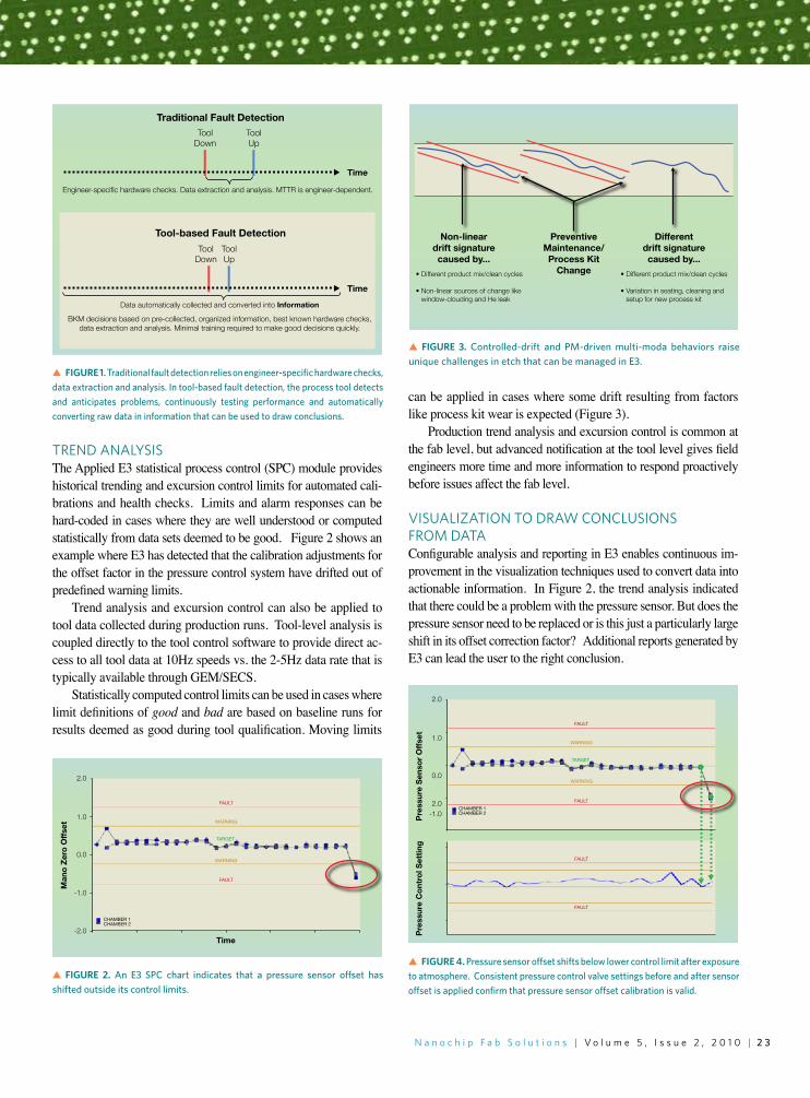
VISUALIzATIoN To DrAW CoNCLUSIoNS FroM DATAConfigurable analysis and reporting in E3 enables continuous im-provement in the visualization techniques used to convert data into actionable information. In Figure 2, the trend analysis indicated that there could be a problem with the pressure sensor. But does the pressure sensor need to be replaced or is this just a particularly large shift in its offset correction factor? Additional reports generated by E3 can lead the user to the right conclusion.
FIGURE 1▲ Traditional fault detection relies on engineer-specific hardware checks, data extraction and analysis. In tool-based fault detection, the process tool detects and anticipates problems, continuously testing performance and automatically converting raw data in information that can be used to draw conclusions.
Man
o Z
ero
Off
set
Time
CHAMBER 1CHAMBER 2
2.0
1.0
0.0
-1.0
-2.0
FAULT
WARNING
TARGET
FAULT
WARNING
FIGURE 2 ▲ An E3 SPC chart indicates that a pressure sensor offset has shifted outside its control limits.
Non-lineardrift signaturecaused by...
• Different product mix/clean cycles
• Non-linear sources of change like window-clouding and He leak
PreventiveMaintenance/Process Kit
Change
Differentdrift signaturecaused by...
• Different product mix/clean cycles
• Variation in seating, cleaning and setup for new process kit
FIGURE 3 ▲ Controlled-drift and PM-driven multi-moda behaviors raise unique challenges in etch that can be managed in E3.
FIGURE 4 ▲ Pressure sensor offset shifts below lower control limit after exposure to atmosphere. Consistent pressure control valve settings before and after sensor offset is applied confirm that pressure sensor offset calibration is valid.
Pre
ssur
e S
enso
r O
ffse
t
CHAMBER 1CHAMBER 2
2.0
1.0
0.0
-1.0
FAULT
FAULT
TARGET
FAULT
FAULT
Pre
ssur
e C
ont
rol S
etti
ng
2.0
WARNING
WARNING

| V o l u m e 5 , I s s u e 2 , 2 0 1 0 | N a n o c h i p F a b S o l u t i o n s2 4
Authors: Todd Egan, Barry Craver, Dermot Cantwell. For additional information, please contact [email protected].
The E3 report in Figure 4 shows no significant change in pressure control settings after the new pressure sensor offset is applied. This helps to confirm that the offset correction is valid. The shift in pressure sensor readings after exposure to atmosphere through a chamber vent history report could also be used to fortify the conclusion that this offset correction is valid. Multiple data traces organized into these types of reports guide the user to a conclusion that would previously have required manual data extraction, analysis and expert-level knowledge of the pressure control system.
This is a practical example of an expert system; it is a process of guiding the user to conclusions through pre-defined analysis and visual-ization techniques. The enabling element here is in how the combination of data storage, analysis tools and configurability in E3 facilitates the migration of engineering knowledge onto the etch tool.
AUToMATIoN oF ExISTINg rEPorTSE3 also simplifies the archiving and reporting of benchmark test data that was previously transcribed manually into a spreadsheet. Automation reduces the time required to qualify a new tool and it facilitates subsequent comparisons against the benchmark readings during troubleshooting. Using this tool, field engineers spend less time clicking, copying and pasting and more time thinking. Figure 5 shows an automated acceptance report for an RF subsystem that has shifted after initial setup.
INTErACTIVE DATA ANALySIS AND MININgPredefined analysis and visualization strategies frequently show no clear trend or correlation to mismatched on-wafer results. In these cases, newly introduced data mining capabilities in E3 facilitate more efficient navigation of large data sets. Data mining tools can be used to rank degrees of difference in large data sets, avoiding the need to look through hundreds of individual charts to find the most likely sources of variation.
The analysis shown in Figure 6 ranks SPC data by proximity to control limits, enabling an engineer to efficiently review a large data set, starting with the data that is most suspicious as defined by its proxim-ity to its control limits. A less obvious, but equally valuable aspect of data mining is the ability to quickly determine that the answer may not lie in the data. This can point an engineer to a need for additional metrology or sensor feedback to improve the tool’s ability to predict on-wafer results with data.
CoNCLUSIoNToday’s engineers commonly conduct chamber matching analyses of-fline using text files and spreadsheets. Because there isn’t enough time or knowledge to assemble the information and expertise required to make the best decision, engineers often resort to hit-or-miss approaches to problem solving. Too often, the best chamber matching knowledge remains in the minds and spreadsheets of a few engineers.
E3 facilitates tool-level generation and retention of chamber matching knowledge through configurable fault detection, data analysis and visualization that can be distributed and matured through ongoing cycles of improvement. In cases where dynamic limit checking and reporting don’t reveal the source of a matching issue, interactive E3 analysis and data mining tools can enable experienced engineers to draw additional conclusions from tool data. Conclusions may range from requirements for additional charts or analysis models in E3 to the need for improved process visibility through advanced sensors. Chamber matching maturity is driven by cycles of learning as conclu-sions from interactive and offline failure analysis drive improvements in automated tool-level diagnostics. The value of Applied E3 grows as more matching issues are detected in less time and unscheduled tool down time decreases. n
FIGURE 5 ▲ RF phase shift from baseline test data detected in Applied E3.
4912
9827
14741
19655
24569
29483
34397
39311
44225
49139
540530.0 0.5 1.0 1.5 2.0 2.5 3.0 3.5 4.0
ResultUpper Critical2
Lower Critical2
Upper Warning1
Lower Warning1
Target0
Upper Outlier3
Lower Outlier3
Result
Pareto UVA results by proximity to control limits
2.40
2.20
2.25
2.30
2.35
2.15
2.00
2.10
0 90 180
Underlying Sensor Data
FIGURE 6 ▲ Automatic ranking of sensor data by its proximity to control limits facilitates efficient navigation of large quantities of sensor data.
DC
Bia
s
95
85
90
80
70
75
0 90 180 270 360RF Bias CEX Phase
Phase shifted by 15 degrees from Tier 1 Report
DC
Bia
s
100
90
80
700 90 180 270 360
RF Bias CEX Phase

N a n o c h i p F a b S o l u t i o n s | V o l u m e 5 , I s s u e 2 , 2 0 1 0 | 2 5N a n o c h i p F a b S o l u t i o n s | V o l u m e 5 , I s s u e 2 , 2 0 1 0 | 2 5
Reporter’s Notebook: ISMI Manufacturing Week
Sonderman’s keynote also introduced a new acronym: DEM, or design-enhanced manufacturing. By using feed-forward and feed-back loops between the design and the manufacturing tools, GLOBALFOUNDRIES believes it can adjust the manufacturing process to the needs of a particular design.
“We want to reach a level of agility where we can tune our manufacturing process to exactly what a customer needs,” said Sonderman. For example, if a design requires a film thickness in the upper right hand corner instead of the middle of the process window, then GLOBALFOUND-RIES will endeavor to tune its process to deliver the best configuration for that design. Is this doable in a foundry? Time will tell if foundries, with their high mix and frequent change of products, can be that agile.
Virtual metrology (VM) is worth pursuing with more intensity, according to Sonderman, partly because integrated metrology is proving too expensive. VM relies on data from multiple status vari-able IDs (SVIDs) regarding temperature, power, pressure, and other inputs to come up with a predictive metrology value. It leverages information already coming from the tool to predict, for example, the film thickness of a CVD step. VM requires what Sonderman called “dynamic adaptive sampling.” Using VM, Sonderman believes GLOBALFOUNDRIES can achieve its goal of wafer-level control without the expense of integrated metrology.
He also called for faster progress on multivariate analysis, which is the analysis of more than one SVID at a time. Analyzing data coming from multiple sources hasn’t taken off, he said, arguing that the industry needs to consider how to apply multivariate analysis to run-to-run control and fault detection in the same system.
David Stark, manager of the Prognostics and Health Management (PHM) program at ISMI, moderated a detailed discussion of two ISMI pilot programs in which a tool vendor, an IDM, and a university col-laborated on the study of predictive maintenance techniques. “These are real tools, in real fabs, running real processes, not some laboratory setup,” Stark emphasized. A long-term PHM goal is to develop a dashboard that
provides information about tool health by displaying data on heat, temperature, and many other indicators. The data also would help predict when key parts are about to fail.
Environmental, safety and health (ESH) issues were on the minds of many conference attendees. ISMI has a strong ESH program, which includes turning off pumps in the subfab when tools are idling. During an executive panel discussion on ESH, Sanjiv Mittal, managing director of the FabVantage™ consulting group at Applied Materials, noted that the Applied iSYS™ integrated abatement and vacuum pumping system works seamlessly with wafer processing equipment, reducing power consumption and emissions when tools are in idle mode.
Fab managers at the conference indicated that they need more data to get comfortable with throttling down pumps or shutting them off completely. Norm Armour, vice president and general manager of GLOBALFOUNDRIES Fab 8, now under construction, supports the approach and said he wants to “see lots of data from alpha and beta test sites—and we need to develop internal evaluation systems so we can run our own assessments,” ensuring that sensitive processes are not impacted by stopping and restarting sub-fab modules. However, Steve James, manager of the Texas Instruments DFAB in Dallas, said, “We are hungry for it. Sometimes we are idling tools for weeks or months, but the pumps are still running. We would love to see [integrated abatement and pumping].” Mittal concurred, saying, “we have got to continue to measure performance” to make sure fab managers have the data they need to support this approach.
Overall, ISMI Week showed how managers, prompted by competitive pressures and the need for green manufacturing, are quickly adapting the way they operate their fabs. n
Author: David Lammers. Journalist David Lammers has been writing about the semiconductor industry since 1980. He has worked for The Associated Press, E.E. Times, and Semi-conductor International magazine, including a 19-year-period in Tokyo.
The Last Word
I n early November the seventh annual ISMI Manufacturing Week in Austin, TX, brought together several hundred productivity technologists and a number of fab managers for four days of presentations and networking. The event began with a call by Tom Sonderman, vice president of manufacturing systems and technology at GLOBALFOUNDRIES, for
faster progress on predictive maintenance and virtual metrology, and tighter links between design and manufacturing.
Tom Sonderman, ▲
VP Manufacturing Systems & Technology, GLOBALFOUNDRIES

www.appliedmaterials.com Printed on recycled Paper AgS-NFS-1110-001 11/10 3.2k