Embed Size (px)
Citation preview
Thanh Van
INTEGRATING HETEROGENEOUS
IOT DEVICES TO IOT PLATFORM
School of Technology 2021

ACKNOWLEDGEMENTS
I would like express my greatest gratitude to Dr. Gao Chao for his help and
guidance over the years which is unmeasurable. Without his support, I
would not be where I am today. It has been an honour for me to be his
student.
I would also like to express my appreciation to Ph.D. Peter von Wrycza, and
MSc. Ari Keränen for giving me the golden opportunity to work on this won-
derful project.
I am extremely thankful and pay my gratitude to DSc. Petri Laari for his
guidance and advice which carried me through all the stages of writing my
thesis.
I would like to express my sincere appreciations to MEng. Christer
Holmberg for not only his support, encouragement, and thoughtful supervi-
sion throughout this thesis implementation but also his dedication and en-
thusiasm as a mentor that gave me a lot of inspiration in my career path.
I wish to extend my appreciation to Mr. Hiroshi Doyu, Mr. Davide Piscopo,
as well as Mr. Joakim Uddenfeldt and Mr. Douglas Boiling from the Ardesco
Team for their cooperation and support. I could not have accomplished all
the assigned tasks without their help.
From the deepest part of my heart, I would like to say a special thank you
to my family for raising me to be a good person. I would also like to thank
all teachers, staffs, and my friends at VAMK, University of Applied Sciences.
Thank you for accompanying me on a long journey.
Espoo, Finland.
17.05.2021

VAASAN AMMATTIKORKEAKOULU UNIVERSITY OF APPLIED SCIENCES Information Technology
ABSTRACT
Author Thanh Van Title Integrating Heterogeneous IoT Devices to IoT Platform Year 2021 Language English Pages 55 Name of Supervisor Dr. Gao Chao
In this thesis, the focus is on integrating heterogeneous IoT devices to an IoT platform inside the Ericsson IoT Technologies Research team. The thesis looked at solving the compatibility problem between various IoT de-vices and an IoT Platform within the IoT universe by enabling the Plug and Play program on multiple devices running on different operating systems.
The Plug and Play program allows the integration of peripherals to the IoT ecosystem without human interaction and extends the end-to-end commu-nication from Server-Device to Server-Peripherals interactions. The inte-gration of devices in this thesis was directly contributed to the Ericsson Research’s IoT Program’s 2020 demonstrator. The idea and the right of accessing internal tools used in this project were provided by Ericsson.
As a result, the thesis work met the set of requirements. Moreover, the thesis identified also new improvements ideas and developed further the implementation. The Plug and Play program on the Ardesco can be used for testing and to further develop as a standard feature supported by the Ardesco devices. When working with the platforms supported by the Plug and Play program, the integration of heterogeneous IoT devices to IoT platform is faster and requires less human intervention than traditional so-lution.
Keywords IoT, microcontrollers, RTOS, wireless communication
CONTENTS
ABSTRACT
1 INTRODUCTION ................................................................................. 9
1.1 Thesis Introduction ........................................................................ 9
1.2 Ericsson Company Presentation ................................................. 10
1.3 Plug and Play Solution within Ericsson IoT Program................... 10
2 THEORITICAL FRAMEWORK ........................................................... 12
2.1 Internet of Things ........................................................................ 12
2.2 Communication Technologies ..................................................... 13
2.2.1 Lightweight Machine to Machine Protocol ........................ 13
2.2.2 Long-Term Evolution Standard ......................................... 17
2.2.3 I2C .................................................................................... 17
2.3 Hardware ..................................................................................... 19
2.3.1 Freedom-K64F.................................................................. 19
2.3.2 Ardesco Prototype ............................................................ 20
2.3.3 Ardesco Combi Dev .......................................................... 21
2.4 Operating Systems ...................................................................... 22
2.4.1 Mbed Operating System ................................................... 22
2.4.2 Zephyr Operating System ................................................. 23
2.5 Software ...................................................................................... 23
2.5.1 ARM Mbed tools ............................................................... 23
2.5.2 nRF Connect SDK ............................................................ 24
2.6 Plug and Play .............................................................................. 25
2.6.1 PnP Hardware Architecture .............................................. 26
2.6.2 PnP Software Architecture ................................................ 27
3 IMPLEMENTATION ........................................................................... 30
3.1 Hardware System Architecture .................................................... 30
3.2 Implementation Plan.................................................................... 31
3.3 Reinstall the PnP Program on FRDM-K64F ................................ 32
3.3.1 The Requirements ............................................................ 32
3.3.2 Compiling the PnP Program on Mbed OS ........................ 33

3.3.3 Operating the PnP Program on Mbed OS ....................... 33
3.4 PnP platform Switching Process on the Ardesco ........................ 34
3.4.1 LwM2M Client Implementation.......................................... 34
3.4.2 Communication between Ardesco and Peripherals. ......... 36
3.4.3 Ardesco Serial Communication Constraints and Solution . 38
3.4.4 Modifying the Original PnP Library. .................................. 40
3.4.5 Description File Structure ................................................. 43
4 ADDITIONAL HARDWARE IMPLEMENTATION ............................... 45
4.1 Additional Hardware System Design ........................................... 45
4.2 Additional Hardware System Circuit Schematic .......................... 46
5 PROJECT OUTCOMES ..................................................................... 48
6 OUTSTANDING PROBLEMS AND SOLUTION SUGGESTIONS ..... 50
6.1 The Description File within the Ardesco Environment ................. 50
6.2 Compiled Version of the Description File .................................... 50
7 CONCLUSIONS ................................................................................. 51
REFERENCES ........................................................................................ 52

LIST OF FIGURES
Figure 1. LwM2M Interfaces /5/ .................................................................... 14
Figure 2. LwM2M Data Model /6/ ................................................................. 16
Figure 3. I2C Protocol /10/ ............................................................................. 18
Figure 4. Freedom-K64F development board ............................................ 19
Figure 5. Ardesco Prototype .......................................................................... 20
Figure 6. Ardesco Combi Dev ....................................................................... 21
Figure 7. Original PnP implementation architecture .................................. 26
Figure 8. PnP operation sequence ............................................................... 28
Figure 9. Hardware implementation ............................................................. 30
Figure 10. Ardesco Prototype before and after soldering an external
connector ........................................................................................................... 37
Figure 11. MPU6050 Temperature Description File .................................. 43
Figure 12. MPU6050 Accelerometer Description File ............................... 44
Figure 13. Upgraded hardware system with additional hardware
components ....................................................................................................... 45
Figure 14. Additional hardware circuit schematic ...................................... 46
Figure 15. Additional hardware prototypes with closed cover ................. 48
Figure 16.Additional hardware prototypes with opened cover ................. 48
7
LIST OF ABBREVIATIONS
2G/3G/4G Generations of wireless technology for digital cellular net-
work
API Application Programing Interface
ARM Advanced RISC Machine
CAT-M LTE Category M
CLI Command-Line Interface
CoAP Constrained Application Protocol
CoRE Constrained RESTful Environments
EEPROM Electronically Erasable Programmable Read-Only Memory
FOTA Firmware Over-The-Air
GDB GNU Debugger
GPIO General-Purpose Input/Output
I2C Inter-Integrated Circuit
IC Integrated Circuit
ICT Information and Communication Technologies
IDE Integrated Development Environment
IoT Internet of Things
LED Light Emitting Diode
LSB Least Significant Bit
LTE Long Term Evolution
LwM2M Lightweight Machine to Machine
MCU Microcontroller Unit
MSB Most Significant Bit
NB-IoT Narrowband Internet of Things
OMA Open Mobile Alliance
OS Operating System
PCB Printed Circuit Board
PnP Plug and Play
RTOS Real Time Operating System
SCL Serial Clock Line
SDA Serial Data Line
SPI Serial Peripheral Interface
SiP System in Package
SoC System on a chip
UART Universal Asynchronous Receiver Transmitter

9
1 INTRODUCTION
1.1 Thesis Introduction
Internet of Things (IoT) is currently a well-known term and is becoming a
core part of human life. The proliferation of IoT prototypes and devices on
the consumer market is the clearest proof that shows the demand in con-
nectivity of human in this era. As a growing number of heterogeneous de-
vices support the IoT concept, it takes more effort to make them compati-
ble with the IoT platform and interoperable with each other, which have
been identified as the main obstacles in the progress so far. The integra-
tion process of new hardware devices has not really changed during the
past years. It requires a lot of effort from an engineer with a good experi-
ence in embedded layer while being time consuming at the same time.
This thesis describes the work aiming at converting the integration of pe-
ripheral devices from a standard process to a new stage, which is simpler
and is not requiring any hardware modification to the existing peripherals.
Solving the compatibility issue could be considered as a key feature to
unlock the true potential of IoT. It can make IoT ecosystems more scalable
by enabling connecting all the existing hardware devices on the market
within the available IoT environment. Furthermore, reducing engineering
effort during the new device integration phase assists in accelerating IoT
prototyping time, thereby reducing time to market which finally makes the
product more competitive in the market.
This thesis continued from previous work in Ericsson with the design and
implementation of a novel IoT plug and play solution. The material and
data for this work is fully provided by Ericsson IoT Technologies Research,
which includes Plug and Play program source code, Ericsson Internal De-
vice, such as Ardesco Prototype and Ardesco Combi Dev, and the access
right to Ericsson confidential documents.

1.2 Ericsson Company Presentation
L M Ericsson Telephone Corporation is a Swedish multinational network-
ing and telecommunications company founded in 1876 and it is one of the
leading manufacturers of delivering Information and Communication Tech-
nology solutions (ICT) to service providers. Ericsson owns more than
39,000 patents with a large hold on standards patents for mobile commu-
nication systems which covers the systems from 2G to 5G and beyond.
Ericsson operates through four major business segments: Networks, Dig-
ital Services, Managed Services, and Emerging Business. Ericsson’s Net-
work portfolio includes hardware, software, solutions, and related service
offerings, where Ericsson’s Cellular IoT solution provides cellular connec-
tivity to low complexity IoT devices based on Narrowband Internet of
Things (NB-IoT) and LTE Category M (CAT-M) technologies. Cellular IoT
solution opens the door for new Mobile Broadband use cases, which is
applied in advanced industrial automation applications of global manufac-
turers. /1/
1.3 Plug and Play Solution within Ericsson IoT Program
Integrating heterogeneous peripheral IoT devices to an IoT platform
played an importance role in the demonstrator of ER IoT Technologies
Research team in the late 2020. In a traditional way, hardware integration
always requires a direct intervention in embedded systems with every new
hardware device coming into the ecosystem, which is time consuming and
not effective. It is obvious that the integrating process needed to be
evolved. To solve that problem, Ericsson has developed a Plug and Play
solution that allows the integration of heterogeneous peripheral devices to
the IoT platform without human interaction and further extended the com-
munication from Server-Device to Server-Peripheral interaction.

11
However, the original Plug and play implementation supported only a lim-
ited number of operating systems and devices. Hence, the application
needed to be ported to Zephyr Operating System which is an Ericsson
main target environment for Ericsson IoT devices. This thesis supported
enabling large scale IoT device deployment with zero cost, which is useful
for the IoT Program’s 2020 demonstrator of the Ericsson IoT research
team.

2 THEORITICAL FRAMEWORK
This section describes shortly the IoT concept and the technologies that
are relevant to this work including the hardware, software, and communi-
cation technologies.
2.1 Internet of Things
Internet of Things (IoT) is a system in which physical devices are con-
nected to the Internet with the ability to collect and share real-time data
without the requirement of human interaction. The physical devices in this
term are diversified, they can be for example analog or digital. There is a
number of digital devices in the IoT ecosystem that people familiarize with
the device naming, such as “smart”, for example smart phone, smart
watch, smart TV. However, even an analog device, such as an electrical
lightbulb can be turned into a smart lightbulb by adding sensors and an
internet connection module, which also adds a level of digital intelligence
to the device and makes it easier to operate the device over the network.
Nowadays, the term IoT is gradually becoming popular by the involvement
of hardware devices from different manufacturers in the consumer market.
The latest development has also merged the analog and digital environ-
ments, enabling even more devices to be connected to the Internet. This
is not only contributing to the diversity of the IoT ecosystem, but also re-
quiring the data transfer technologies to be evolved to adapt different com-
munication needs. The following sections introduce all the communication
technologies and protocols which have been applied in this thesis work.
/2/
13
2.2 Communication Technologies
This section describes the protocols and data models used for communi-
cating from the peripheral devices to the LwM2M Client and further to the
LwM2M Server over the cellular network that are relevant to this thesis.
2.2.1 Lightweight Machine to Machine Protocol
Light weight machine to machine (LwM2M) is an Open Mobile Alliance
(OMA) standardized protocol, the development of which has been sup-
ported by Ericsson from the early phases. LwM2M delivers a common
standard for managing low power and constrained devices on a variety of
networks to exploit the potential of IoT. LwM2M is designed for remote
management of M2M devices and related service. Using an architecture
based on REST, LwM2M defines an extensible resource and data model
and builds on a data transfer protocol called the Constrained Application
Protocol (CoAP). LwM2M provides a solution for more complex, long term
and large-scale IoT use case involving heterogeneous hardware deploy-
ments. /3, 4/
The LwM2M standard architecture defines three entities (see Figure 1):
• LwM2M Client
• LwM2M Server
• LwM2M Bootstrap-Server
Four interfaces have been designed between the different entities:
• Bootstrap
• Client Registration
• Device Management and Service Enablement
• Information Reporting

Figure 1. LwM2M Interfaces /5/
LwM2M Client This logical component is often implemented in IoT
devices and gateways, and it serves as an endpoint of the LwM2M proto-
col and interacts with the LwM2M Server and the LwM2M Bootstrap
Server.
LwM2M Server This server is a software component which is typically
running on a non-IoT device, it implemented the functionality of the server-
side for interacting with a LwM2M Client.
LwM2M Bootstrap-Server This component is a server for provi-
sioning essential information for a LwM2M Client, such as credentials.
Typically, the LwM2M Bootstrap-Server is the first LwM2M entity that a
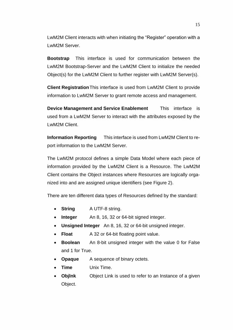
15
LwM2M Client interacts with when initiating the “Register” operation with a
LwM2M Server.
Bootstrap This interface is used for communication between the
LwM2M Bootstrap-Server and the LwM2M Client to initialize the needed
Object(s) for the LwM2M Client to further register with LwM2M Server(s).
Client Registration This interface is used from LwM2M Client to provide
information to LwM2M Server to grant remote access and management.
Device Management and Service Enablement This interface is
used from a LwM2M Server to interact with the attributes exposed by the
LwM2M Client.
Information Reporting This interface is used from LwM2M Client to re-
port information to the LwM2M Server.
The LwM2M protocol defines a simple Data Model where each piece of
information provided by the LwM2M Client is a Resource. The LwM2M
Client contains the Object instances where Resources are logically orga-
nized into and are assigned unique identifiers (see Figure 2).
There are ten different data types of Resources defined by the standard:
• String A UTF-8 string.
• Integer An 8, 16, 32 or 64-bit signed integer.
• Unsigned Integer An 8, 16, 32 or 64-bit unsigned integer.
• Float A 32 or 64-bit floating point value.
• Boolean An 8-bit unsigned integer with the value 0 for False
and 1 for True.
• Opaque A sequence of binary octets.
• Time Unix Time.
• Objlnk Object Link is used to refer to an Instance of a given
Object.

• Corelnk Constrained RESTful Environments Link (CoRE Link)
is used to refer to Resources on a LwM2M Client.
• none It exclusively concerns Executable Resource.
Figure 2. LwM2M Data Model /6/
The Data Model defined three Resource operations supported by the
LwM2M Server:
• Read/Observe Used to read the current values.
• Write Used to change/update values.
• Execute Used to initiate an action.

17
2.2.2 Long-Term Evolution Standard
Long-Term Evolution (LTE) is a wireless broadband communication stand-
ard for mobile devices. LTE offers higher network capacity and speed to
mobile device users in comparison with the third generation of wireless
mobile telecommunications technology (3G). LTE is well known as 3.95G
to separate it from the fourth generation of wireless mobile telecommuni-
cations technology (4G), implying LTE as a standard that is close to ap-
proaches 4G. There are a variety of LTE Categories used to describe dif-
ferent LTE network capabilities where LTE-Cat-M1 and LTE-Cat-NB1 are
the most popular protocols applied in the cellular IoT industry. /7/
LTE-Cat-NB1, also officially known as Narrowband IoT (NB-IoT) is a Low
Power Wide Area (LPWA) cellular technology operating in narrow band-
width (200kHz) and it is not compatible with the existing LTE network,
hence it requires a high upfront cost to deploy NB-IoT. However, NB-IoT
is a potentially less expensive option in long-term operation because it
eliminates the need for a gateway, which allows sensor data to be sent
directly to the primary server. /8/
Just like NB-IoT, LTE-Cat-M1 (Cat-M1) is also a Low Power Wide Area
(LPWA) cellular technology. Cat-M1 operates at 1.4 MHz bandwidth with
higher device complexity and cost than NB-IoT but it is compatible with the
existing LTE network. The wider bandwidth allows Cat-M1 to achieve
greater data rate, lower latency, and more accurate device positioning ca-
pabilities. Furthermore, Cat-M1 supports voice calls and offers a lot of po-
tential benefits and use scenarios within a low cost and long battery life
IoT device. /9/
2.2.3 I2C
Inter-Integrated Circuit (I2C) is a two-wire serial embedded communication
technology which is a world standard implemented in over 1000 different
Integrated Circuit (IC) products by over 50 manufacturers. This technology
aims to connect low-speed devices, such as microcontroller, Electronically
Erasable Programmable Read-Only Memory (EEPROM), D/A and A/D
converters, I/O interfaces, and similar peripherals devices within embed-
ded systems.
I2C uses a bidirectional 2-wire bus for communication between master(s)
and slave(s), one master can control multiple slaves, and one slave can
be controlled by multiple masters on an I2C bus. A slave device will trans-
mit data after it has been addressed by the master. Every slave device on
the same I2C bus has a unique address to make a separation between
different sending devices. Each slave device has also internal register
maps that have unique register addresses, where the master can access
to configure the slave behavior.
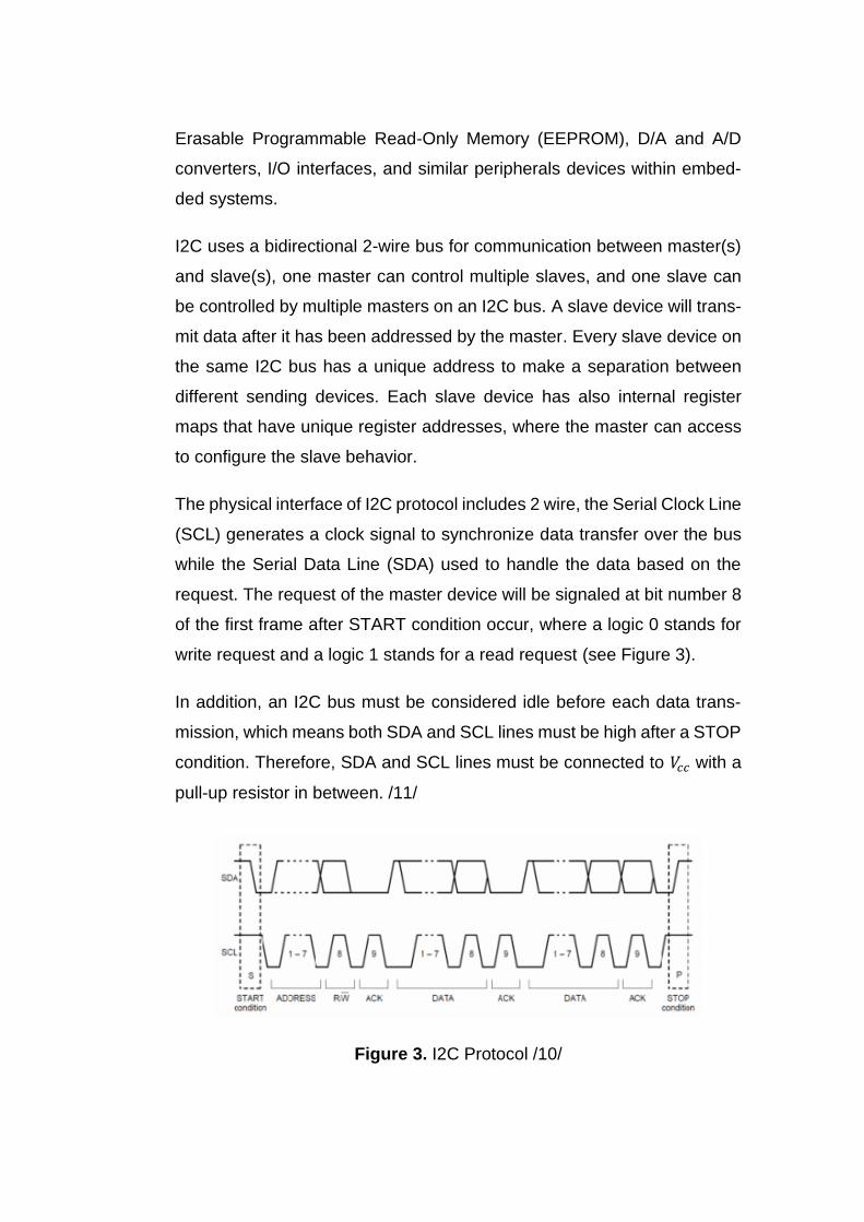
The physical interface of I2C protocol includes 2 wire, the Serial Clock Line
(SCL) generates a clock signal to synchronize data transfer over the bus
while the Serial Data Line (SDA) used to handle the data based on the
request. The request of the master device will be signaled at bit number 8
of the first frame after START condition occur, where a logic 0 stands for
write request and a logic 1 stands for a read request (see Figure 3).
In addition, an I2C bus must be considered idle before each data trans-
mission, which means both SDA and SCL lines must be high after a STOP
condition. Therefore, SDA and SCL lines must be connected to 𝑉𝑐𝑐 with a
pull-up resistor in between. /11/
Figure 3. I2C Protocol /10/

19
2.3 Hardware
This section describes the detailed information of the target devices used
during the implementation work. The two devices are the Freedom-K64F
device, which was used to develop the first prototype of the Plug and Play
program previously, and the Ardesco device, which is the new platform
target of the Plug and Play solution.
2.3.1 Freedom-K64F
Figure 4. Freedom-K64F development board
The Freedom-K64F (FRDM-K64F) is a Flagship of ultra-low-cost develop-
ment platform for Kinetis K64, K63, and K24 Microcontroller Units (MCUs)
designed by NXP. The board has been optimized for connected applica-
tions by using power-efficient Kinetis K64F MCU featuring an Advanced
RISC Machine (ARM) Cortex-M4 core running up to 120 MHz. For more
details, the board has 1024 KB Flash, 256 KB RAM, and a wide-list of
peripherals, such as 16-bit ADCs, DAC, timers, also many interfaces, such
as Ethernet, USB Device Crystal-less and Serial.
The FRDM-K64F board is packaged as a development board including
extension headers compatible with Arduino UNO Rev3 shields and in-
cludes a built-in USB Debug and Flash Programmer on CMSIS-DAP inter-
face chip. To enable rapid prototyping, the board is integrated with a 6-
axis digital accelerometer and magnetometer for full eCompass capabili-
ties, two user push-button for direct interaction, a microSD card slot, and
an onboard Ethernet port of RJ45 standard cable. /12/

2.3.2 Ardesco Prototype
Figure 5. Ardesco Prototype
The Ardesco Prototype board is a cellular IoT reference device platform
developed in cooperation between Ericsson and Sigma Connectivity. The
prototype aims to simplify and accelerate design process for cellular native
IoT devices and also efficiently deploy and manage devices over their
complete life cycle. The Ardesco board development process is divided
into several phases. The Ardesco Prototype is a pre-release sample ver-
sion, where the focus has not yet been on setting up and maintaining the
board, thus the development environment is rather complicated. The pro-
totype version does not yet fully support all the planned features.
The Ardesco Prototype device operates on a combination of the nRF9160
low power System-in-Package (SiP) and nRF52840 System-on-a-Chip
(SoC) as a support chip for the nRF9160. The nRF9160 chip has an inte-
grated LTE-M/NB-IoT modem operating in multimode and multiple LTE
bands, which also supports firmware upgrades via secure, encrypted Firm-
ware Over The Air (FOTA) updates. The chip allows advanced application
development to become possible in a single device solution thanks to the
ARM Cortex-M33 application processor running up to 64 MHz with 1 MB
of flash and 256 KB RAM. The nRF9160 also has a broad selection of
general interfaces and peripheral including 12-bit ADC, RTC, Serial Pe-
ripheral Interface (SPI), I2C, I2S, UARTE, PDM and PWM. On the other
hand, the nRF52840 is developed around the ARM Cortex-M4 running up
to 64 MHz and offering generous memory availability for both Flash and
RAM. The chip is fully multiprotocol capable with full protocol concurrency
and supports for Bluetooth 5, Bluetooth mesh, Zigbee and so on. It also

21
has numerous digital peripherals and interfaces such as SPI, Universal
Asynchronous Receiver Transmitter (UART), TWI, PDM, I2S, and QSPI.
/13, 14, 15/
On the Ardesco Prototype, the nRF9160 console has been directed out on
UART0 which is connected to UART0 of the nRF52840 Bluetooth chip.
The nRF52840 is also responsible for implementing the USB interface and
the default firmware in the nRF52840 redirects UART0 out one of the two
virtual serial ports that can be accessed with a standard terminal emulator
on the computer.
2.3.3 Ardesco Combi Dev
Figure 6. Ardesco Combi Dev
The Ardesco Combi Dev is the official version to be released, which pro-
vides almost the same features compared to the Ardesco Prototype. The
main differences are a bigger flash memory and a smaller body size.
On the Ardesco Prototype, one limitation is the lack of an external con-
nector for integrating peripheral devices. This constraint does no longer
exist on the Ardesco Combi Dev which has now a Grove connector. Grove
is a modular, standardized connector prototyping system from Seeed Stu-
dio. Grove has an extensive ecosystem of modules from a simple button
to a more complex heart rate sensor. It enables an easy way to connect
the modules to the base unit, generally a microprocessor, through a Grove
standardized connector /16/. The Grove connector on Ardesco has four

physical pins. Two of them are for power supply purpose and the remain-
ing two pins can be configured to map UART or I2C interface, or discrete
General-Purpose Input/Output (GPIO) pins.
One constraint on the Ardesco Combi Dev is that the nRF9160 chip only
supports a total of four serial communicating peripherals simultaneously.
The default configuration on Ardesco Combi Dev maps 2 UART ports of
the nRF9160 to nRF52840 for the USB interface, one SPI port and one
I2C port to the build-in sensors. This does not leave any serial communi-
cation ports to map to the Grove connector. As an alternative, eliminating
one of the UARTs to nRF52840 is considered the most optimal solution
since SPI and I2C are needed to communicate with various built-in sen-
sors of multiple purposes.
2.4 Operating Systems
This section describes two operating systems, Mbed Operating System
and Zephyr Operating System. These operating systems have been cho-
sen by Ericsson Research as the target operating systems for the devices
used in this thesis work.
2.4.1 Mbed Operating System
Mbed Operating System (Mbed OS) is an open-source operating system
designed specifically for constrained and low powered IoT devices that
need to connect to the internet. One of the top advantages of Mbed OS is
providing an abstraction layer for the microcontroller it runs on, which
means Mbed OS applications can be reused on any Mbed enabled plat-
form. Therefore, developers can focus on writing applications in C/C++
that can reuse the similar functionality available on different hardware de-
vices.
Mbed OS provides also a stable core of existing connectivity technologies,
such as Bluetooth Low Energy, LoRA, Ethernet, Wifi, and cellular across
devices and system architecture with Mbed OS applied. /17/

23
2.4.2 Zephyr Operating System
Zephyr Operating System (Zephyr OS) is a best-in-class open source,
small, and scalable Real Time Operating System (RTOS) optimized for
resource-constrained and embedded IoT devices. Zephyr OS supports all
kinds of devices from simple embedded environment observing sensors
or Light Emitting Diode (LED) wearable to sophisticated multiple hardware
architecture, smart watches, and IoT wireless applications.
Zephyr OS is modular and supports multiple architectures. Developers can
tailor or create solutions as they need with a wide range of supported hard-
ware, developer tools, sensors, and device drivers evolved by the commu-
nity. Zephyr OS also includes all the components and libraries needed to
develop a full application, such as a set of protocol stacks (IPv4/IPv6, OMA
LwM2M, and Bluetooth Low Energy), file systems, and firmware updates.
/18/
2.5 Software
This section describes the software and tools to work with the devices and
operating systems selected for the thesis work and described in the previ-
ous section.
2.5.1 ARM Mbed tools
The Mbed OS development ecosystem includes three tools designed to
create, import, and build a project that use Mbed OS throughout the de-
velopment process. The tools are Mbed Studio, Mbed Command-Line In-
terface (Mbed CLI), and the Mbed Online Compiler. /19, 20, 21/
In this thesis, the Mbed CLI is used as a main tool for development process
because of the simplicity of its installation and usage compared to the
Mbed Studio. Furthermore, the Mbed CLI does not require any internet
connection during development process which is the case with the Mbed
Online Compiler.

While the original ARM Mbed tools are incredibly convenient for getting a
project started, they still lack a debugger where the developer can take a
deep look into the operation of the program. The ARM Mbed support team
has suggested two solutions to debug and test the code. The first solution
is to simply use printf statements for observing process from the serial ter-
minal and the second solution is to debug by using another third-party In-
tegrated Development Environment (IDE). Because using printf state-
ments to debug a large program consumes much effort and is not an ef-
fective way, the thesis work used the Visual Studio Code IDE with GNU
Project Debugger (GDB) supported as a debugger. /22/
2.5.2 nRF Connect SDK
The nRF Connect SDK is a software development kit for programming and
debugging cellular IoT and short-range wireless applications applied in
nRF51, nRF52, nRF53, and nRF91 Series devices by Nordic Semiconduc-
tor. The nRF Connect SDK integrates Zephyr RTOS and includes a wide
list of samples, application protocols, protocol stacks, libraries, and hard-
ware drivers. Hence, it offers developers a scalable framework that allows
development of very small software for applications in resource-con-
strained devices and also enables the developers to fully develop powerful
features for advanced application. The nRF Connect SDK offers source
code management with Git and has free SEGGER Embedded Studio IDE
support as well as nRF Command Line Tools. /23, 24/
The SEGGER Embedded Studio IDE provides users a graphic interface
software that is easy to use but it lacks some features, such as the ability
to compile C++ code. Meanwhile, the nRF Command Line Tools provides
a command line interface which is hard to use but more stable. At the be-
ginning of the thesis project, the SEGGER Embedded Studio IDE was cho-
sen as a main development tool but it was later switched to the nRF Com-
mand Line Tools after discovering the problem with not compiling C++ soft-
ware on the SEGGER.

25
2.6 Plug and Play
Nowadays, the term IoT has gradually become popular thanks to the re-
lease of large range of different kinds of IoT devices from many manufac-
turers, which contribute to fully exploiting the potential of the IoT industry.
However, the emergence of wide variety of different kinds of devices, as
well as new communication standards that they are using, leads to the
compatibility problem between peripherals and the IoT platform. Tradition-
ally, the programmers have been working on customizing the device driv-
ers of every new heterogeneous device to make them compatible with the
existing IoT platforms. Furthermore, the different connectivity technologies
on different devices also creates a burden, while it requires lots of work to
adapt and implement different technologies within the environment.
To solve that problem, Ericsson Research has earlier developed a Plug
and Play (PnP) solution (see Figure 7), which plays an important role in
eliminating the manual installation procedures of heterogeneous devices
into the IoT platform. The Plug and Play solution comprises three compo-
nents: a software component running on the IoT device called the PnP
program, a Description File paired with the peripheral and a File Storage.
Within the PnP solution, a new peripheral integration event is triggered by
an attachment event through a physical push button on the IoT device. On
attachment event, the PnP software component running on the IoT device
will retrieve the Description File from an external memory chip, which con-
tains a semantic description of the operation of the peripheral and their
mapping to a data model, as well as information on how to retrieve data
from the peripheral. After retrieving the Description File, the PnP software
compiles the file and stores the compiled version to the File Storage to
keep a state of the already attached peripherals. This grants consistency
between the software model and the hardware configuration and is re-
sistant to crashes and reboots.
The first implementation of the PnP solution was done on the FRDM-K64F
development board with the PnP software written in C++ and a Description

File stored in an EEPROM chip, and The PnP software used a microSD
card on FRDM-K64F to store the compiled Description File. The FRDM-
K64F board communicates with the peripheral device as well as the
EEPROM chip through the I2C protocol and communicates with the
LwM2M Server through an already implemented LwM2M Client over the
wired Internet connection.
2.6.1 PnP Hardware Architecture
The peripheral device used in the sample demonstrator is a temperature
I2C sensor with an EEPROM attached to the same I2C bus storing infor-
mation provided by the sensor (see Figure 7).
Figure 7. Original PnP implementation architecture
The attachment event is triggered by pushing a built-in push button B1 on
the board which further notices the PnP program about the attached new
peripheral. The PnP program on FRDM-K64F then interacts with the
EEPROM chip using its physical address determined at the attachment
time, to retrieve, parse, and compile the Description File and stores the
compiled version to the SD Card on FRDM-K64F device. The PnP pro-
gram with all necessary information registers the suitable LwM2M Object
27
and LwM2M Resources used by the sensor. The PnP program then ex-
poses the real time data of the sensor to the LwM2M Server through the
wired Internet connection.
After the attachment event is completed, the FRDM-K64F board can in
case of a crash or reboot during the actual operation time, retrieve the
compiled description file from the SD card containing the information of the
last attached peripheral. Therefore, the system can continue to function
smoothly without the requirement to trigger the attachment event again.
The built-in B2 button on the FRDM-K64F is used to trigger the detachment
event with reverse logic to deregister peripheral LwM2M Object as well as
Object Resources.
2.6.2 PnP Software Architecture
The PnP program source code contains two library folders responsible for
the interactions between IoT device, peripheral devices, and LwM2M Cli-
ent. The root folders of the libraries are:
• ipso_pnp: This library contains most of the logic for parsing and
compiling the peripheral’s Description File
• mbed_pnp: This library implements the required bus interface and
the storage interface for the complied Description File
The PnP operation PnP sequence diagram is shown in Figure 8.

Figure 8. PnP operation sequence
During the operation time of the IoT device, the attachment event is trig-
gered by the user through a physical button on the IoT device (1) (see
Figure 8). The mbed_pnp tries to access the peripheral memory for the
Description Files through a predefined I2C address (2). The peripheral
memory responds to the read command from the IoT device with the con-
tent of the Description File (3). The ipso_pnp parses the Description File
to read the bus/protocol used by the new attached peripheral (4) and return
the result to mbed_pnp to scan for the specified bus for new addresses.
The ipso_pnp also reads the IPSO Object information and sends the result
to the LwM2M Client (5) to register the resources through a LwM2M reg-
istration interface (6). After establishing the communication with the pe-
ripheral and the LwM2M Server, the ipso_pnp compiles the Description
File and sends the compiled version to mbed_pnp to store it into the SD
card.
The LwM2M Server is now aware that there is a peripheral connected to
the IoT device, and the server can request the peripheral data by issuing
a GET command (7). The IoT device receives the GET request from the
server and executes the hardware sequence specified in the Description

29
File (8). The mbed_pnp sends a read command to the peripheral device
and the peripheral device responds with the corresponding value. The IoT
device receives the peripheral response and applies the conversions de-
fined in the Description File to get the IPSO Object compatible value from
the raw data (9). The LwM2M Client fills the response with value and sends
it to the server (10).
The PnP program handles the problem cases when the IoT device crashes
or reboots during the operation time. The PnP program takes the initiative
to access the SD Card to look for a compiled version of the Description
File instead of waiting for the attachment event to be triggered again by
the user. The implementation of the new peripheral device continues from
(5) without any user intervention needed. As a result, the IoT system be-
comes more robust in recovering after crashes as well as ensures the au-
tomation throughout the IoT device operation.
The first version of the PnP program implemented on FRDM-K64F had an
unresolved limitation when connecting new devices. The limitation was
that the PnP program was unable to detect the attachment of multiple I2C
peripheral simultaneously. After investigation, the reason for this was
found. The problem was the limitation in the scanning new peripheral
mechanism that only allows the PnP program to detect a single address at
a time. As a result, the user must trigger the physical push button for the
attachment and detachment event on every peripheral device. This is un-
practical in an industrial use case, where integrating a large number of
sensors is required. Therefore, as long as the issue is unresolved, the use
case of PnP is still limited and requires user intervention.

3 IMPLEMENTATION
In this chapter, the detailed implementation, system structure, and meth-
ods applied in the thesis are presented. In addition, the challenges in the
implementation process as well as the limitation in the system are also
described.
3.1 Hardware System Architecture
Figure 9. Hardware implementation
The IoT hardware system deployed in the thesis includes two micro-con-
troller boards: Ardesco and FRDM-K64F. Both devices use the I2C proto-
col to establish communication with their external sensors, but the devices
are completely different regarding the operating system, the peripheral
connector type, and wireless communication technology. While the con-
straint on connectivity range still exists on the FRDM-K64F with the wired
connectivity, Ardesco supports a better solution with a build-in cellular
module. With LTE connectivity, the deployment of Ardesco on industrial
IoT systems becomes easier and more convenient, especially with the ad-
vantage of the installation cost when deploying the device into systems at
a large scale. On the other hand, the Grove connector on Ardesco is also
an advantage when integrating peripheral devices to an IoT device and
further to the IoT platform. With the Grove, an external sensor or device
can be easily attached and detached from an IoT device. The installation,
maintenance, and replacement of the peripherals becomes more efficient

31
and cost-effective with the combination of the Grove connector and the
PnP program.
3.2 Implementation Plan
The primary aim of the work is to port the PnP program implemented on
the FRDM-K64F running Mbed OS to the Ardesco running Zephyr OS
while keeping the features that are needed in the demonstration deploy-
ment. After the PnP program has been fully deployed on Ardesco, the im-
plementation process continues to the next phase where the PnP program
is upgraded with new features as well as trying to solve the remaining lim-
itations on the old software version.
The PnP implementation process for Ardesco has been divided into sev-
eral phases. During the first phase, the original PnP implementation is re-
compiled and flashed onto the FRDM-K64F device. The relaunching soft-
ware on the original system is to confirm whether the software is still com-
patible with the Freedom device and the latest Mbed OS version and it
also assists in observing how the original software works. The careful ob-
servations of the behavior between the IoT device, peripherals, and
LwM2M Server facilitates the transition of the original program to a new
operating system, prevent unexpected errors arising as well as preserve
the original features. The next approach phase is to study how to use
Zephyr OS to read external sensors data as well as how to implement a
simple LwM2M Client on Ardesco for basic interactions between the de-
vice and the Leshan LwM2M Server. Mastering the use of Zephyr OS as
well as the Ardesco enables the modified ability to function in detail, which
is needed for modifying the original PnP code to make it compatible with
the new system.
On the other hand, the limitations on the original PnP software sets con-
straints to the use cases when integrating new peripherals because the
number of peripherals is limited. Thus, the PnP program needs to be up-

graded once the implementation is ready on the Ardesco. The next imple-
mentation phase focus on upgrading the software to meet the require-
ments of the thesis topic by solving the outstanding problems.
3.3 Reinstall the PnP Program on FRDM-K64F
This section describes the requirements to install the PnP software on
FRDM-K64F devices and analyze the behavior of the software.
3.3.1 The Requirements
Preparing the old PnP implementation to be redeployed and tested re-
quires many hardware and software components, including:
• A FRDM-K64F device
• An I2C sensor
• An EEPROM chip
• Mbed CLI tools
• Local debug toolchain (GDB on Visual studio code)
• PnP library source code
The Description File is written to the EEPROM through a simple
write_to_EEPROM program. The write_to_EEPROM program takes the
first text file (“.txt”) in the memory card and then writes the contents of that
text file to the memory chip starting from the first internal address of the
chip. In terms of software, the compiling process and deploying necessary
modules for the PnP program on Mbed OS is performed through the Mbed
CLI tool.
The debugging process with Visual studio code and GDB server is per-
formed during the PnP program run time. During the process, we are trying
to identify the potential bugs in the implementation, as well as observe the
behavior of the PnP program when interacting with the LwM2M Server.

33
3.3.2 Compiling the PnP Program on Mbed OS
During the first try, the PnP program was unable to build successfully with
the newest version of Mbed OS because the evolving nature of the Mbed
OS has led to the alteration of the accompanying modules. Therefore, it is
necessary to retrieve the specific version of Mbed OS used with the origi-
nal PnP implementation. It is clear that the original PnP implementation on
the FRDM-K64F depends heavily on the version of the operating system
and the bundled modules.
3.3.3 Operating the PnP Program on Mbed OS
Using the same version of Mbed OS that was used at the time of the orig-
inal implementation, the PnP program was able to function stably with the
method and sequence of operation as described in Section 2.6.1. To gain
insight into the behavior and the interaction between system components,
a local debug toolchain was used to inspect the program execution.
The PnP implementation has three different parts that needs to be consid-
ered when debugging the program with the GNU Project Debugger (GDB),
namely:
• LwM2M Client operation
• Parsing the Description File and storing the compiled version to the
SD card
• Establishing communication between the IoT device and the periph-
eral
After observing the program activity, we decided to split the original pro-
gram into three smaller modules. Working with the small modules makes
the platform switching process clearer by avoiding unnecessary conflicts
when replacing functions and libraries of the old operating system in the
source code. Thereby, the work can take place smoother and faster, pre-
venting potential bugs during runtime.

3.4 PnP platform Switching Process on the Ardesco
This section describes the modules that were split from the original PnP
as mentioned in the previous section. The modules include: LwM2M Cli-
ent, communication between Ardesco and peripherals, and the PnP li-
brary. Moreover, this section describes also the issues that we faced dur-
ing the modules porting process as well as the solutions.
3.4.1 LwM2M Client Implementation
The LwM2M Client implementation on the Ardesco running Zephyr OS is
one of the mandatory pieces of software to be implemented for the PnP
system. The LwM2M Client procedures involves many stages, including
establishing a connection to the LwM2M Server, registering the Object and
Resources respectively for the attached peripherals, and implementing the
callback events to send and read the external device data from the LwM2M
Server.
Zephyr OS supports deploying a simple LwM2M Client using the functions
and APIs, along with the predefined LwM2M Objects and Resources that
are available in the Zephyr’s LwM2M library. However, using the LwM2M
Objects in the existing library leads to some difficulties in customizing the
Objects as well as their resources without impacting the default library.
Because different devices connected to the system require corresponding
different LwM2M Objects, which are not fully supported by the default
LwM2M library provided by Zephyr OS, enabling the ability to create and
modify existing LwM2M Objects is essential.
To fix the described problem, the library defining LwM2M Objects is re-
placed by a customized library named lwm2m_object, which is based on
the original one and located in the PnP deployment directory. Using the
customized library not only makes it easier to intervene in the Object defi-
nitions but also makes deploying the LwM2M Client on the device more
independent by not having any impact on the existing build-in system. As

35
a result, not being too reliant on Zephyr OS, the native development pro-
cess will make LwM2M Client deployment stable on future versions of
Zephyr OS without much intervention from the developer.
3.4.1.1 Creating New LwM2M Library
The LwM2M library of Zephyr OS offers a wide range of built-in LwM2M
Objects. Each of these LwM2M Objects has a fixed unique ID (Object ID)
and a set of Resource Identifiers (Resource ID) with different functions and
different data types suitable for many purposes. However, Zephyr OS does
not provide any general solution for using the Objects other than calling
individual functions in different Object files to initiate different LwM2M Ob-
jects. That is an inconvenience and lack of consistency when combined
with the PnP library, which requires the ability to initiate suitable LwM2M
Object to the server with only Object ID and Object Instance information.
Therefore, a new LwM2M library was created for the PnP program, which
can register the suitable LwM2M Object as well as its resources based on
the information about Object ID and Object Instance from the user - or to
be more specific, from the Description File in EEPROM.
In the PnP program deployment directory, an LwM2M Object named Gen-
eral Object is in a customized library named lwm2m_object. The General
Object contains a collection of individual Object Resource definitions used
by popular LwM2M Object such as Temperature Object or Accelerometer
Object. All information about Object Resource such as supported opera-
tion or data type is fully provided by the OMA SpecWorks. The General
Object is considered as a general solution to reuse a single LwM2M Object
for many different purposes, which not only makes managing the LwM2M
Object easier but also saves time for integrating new peripherals into the
system.

3.4.1.2 Register New LwM2M Object to LwM2M Server
An LwM2M Object must be registered to the LwM2M Server through its
Object ID to interact with the server. In addition, its Object Resources must
be mapped to a device or a software component for data sharing purposes.
The General Object in the lwm2m_object library works in the same way as
the other LwM2M Objects in the Zephyr LwM2M library. Instead of using
fixed values as a Zephyr sample LwM2M Object, the General Object re-
trieves the information needed to describe the peripheral, such as Object
IDs, Resource IDs from the Description File, followed by resource instruc-
tion sequence such as READ, WRITE, or EXEC. The Resource of the
General Object is mapped to the PnP library to retrieve data from the pe-
ripheral through the sequence of hardware operations defined in the De-
scription File.
After completing the registration of the new LwM2M Object using the
lwm2m_object library the LwM2M Server can perform basic operations
with peripheral devices for data sharing based on the resource instruction
sequence in the Description File. The whole process takes place through
the combination between the lwm2m_object library and the PnP library
with no firmware or software updates needed regardless of which type of
peripheral is attached.
3.4.2 Communication between Ardesco and Peripherals.
Two versions of the Ardesco device were used during the thesis but only
the Ardesco Combi Dev can communicate with the external sensor device
because it has a Grove connector for external use purposes. The Ardesco
Combi Dev can read data from and write to the peripheral through a built-
in I2C library in Zephyr OS. The communication between the Ardesco and
the external device took place smoothly until enabling a library named
BDS, which is required to enable the LTE module for internet connectivity
on the Ardesco device. The BDS caused an unidentified conflict with the
system, which led to an auto-disable Grove connector issue. Hence, the
37
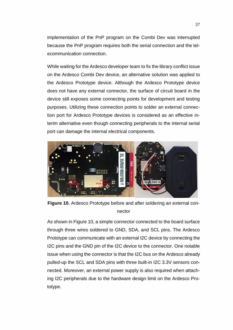
implementation of the PnP program on the Combi Dev was interrupted
because the PnP program requires both the serial connection and the tel-
ecommunication connection.
While waiting for the Ardesco developer team to fix the library conflict issue
on the Ardesco Combi Dev device, an alternative solution was applied to
the Ardesco Prototype device. Although the Ardesco Prototype device
does not have any external connector, the surface of circuit board in the
device still exposes some connecting points for development and testing
purposes. Utilizing these connection points to solder an external connec-
tion port for Ardesco Prototype devices is considered as an effective in-
terim alternative even though connecting peripherals to the internal serial
port can damage the internal electrical components.
Figure 10. Ardesco Prototype before and after soldering an external con-
nector
As shown in Figure 10, a simple connector connected to the board surface
through three wires soldered to GND, SDA, and SCL pins. The Ardesco
Prototype can communicate with an external I2C device by connecting the
I2C pins and the GND pin of the I2C device to the connector. One notable
issue when using the connector is that the I2C bus on the Ardesco already
pulled-up the SCL and SDA pins with three built-in I2C 3.3V sensors con-
nected. Moreover, an external power supply is also required when attach-
ing I2C peripherals due to the hardware design limit on the Ardesco Pro-
totype.

3.4.3 Ardesco Serial Communication Constraints and Solution
In theory, an I2C bus can support multiple peripherals as long as they are
configured to different I2C addresses. However, many I2C sensors in the
consumer market have either a fixed I2C address or only support configu-
ration up to two or three different I2C addresses. For that reason, it is in-
capable to have ten I2C sensors of a type connected on the same I2C bus
because the I2C address is unable to be duplicated. Though, the use of
multiple sensors with the same I2C address is very common in real-life use
cases. An example is the use of multiple temperature sensors of the same
type to measure the temperature of different areas in a building. As a com-
mon solution, these sensors are controlled by only one master device that
supports multiple I2C buses.
As introduced in Section 2.5.2, both versions of the Ardesco device use
the same architecture with the combination between the nrf9160 and the
nrf52840. Therefore, the Ardesco Prototype and the Ardesco Combi Dev
share the same limit of four available serial ports, which finally leaves only
one port for connecting external devices. Hence, it is necessary to expand
the ability to provide more I2C buses on the Ardesco equipment.
Connecting the Ardesco to an I2C 8-channel multiplexer chip is considered
as a solution to provide the possibility to expand the number of available
I2C buses. The TCA-9548A multiplexer supports expansion to eight I2C
buses from one I2C bus by mapping this original I2C bus to one of the
eight output buses through a bus selector on the chip. The Ardesco device
controls the bus selector by sending a byte of instruction data with the Most
Significant Bit (MSB) represents bus number 7, and the Least Significant
Bit (LSB) represents bus number 0. Enabling each separate I2C bus com-
bining a conditional loop allows the Ardesco to communicate with eight
devices with the same I2C address simultaneously.

39
On either version of the Ardesco, there are no free GPIO pins for connect-
ing simple 1-wire devices, such as digital sensors, LEDs, switches, or re-
lays if the connector is configured as I2C. The lack of an additional port for
connecting simple digital devices is a disadvantage on the Ardesco, which
is not only reducing the abundance of peripheral types on the Ardesco but
also reducing the versatility of the device in real-life application. On the
other hand, if the external connector on the Ardesco is configured as nor-
mal GPIO, there are still only two GPIO pins provided by the connector.
The solution is not effective since the Ardesco device is expected to handle
multiple heterogeneous peripheral devices. Therefore, it is necessary to
have an optimal solution that can support analog, digital and I2C connec-
tion operating in parallel as well as expands the number of available GPIO
pins on the Ardesco.
In this case, an I2C GPIO expander from Microchip Technology can pro-
vide eight more GPIO pins for the Ardesco through the I2C protocol as a
standalone peripheral with a unique I2C address. The Ardesco can enable
the GPIO pins as either inputs or outputs by sending the I/O configuration
bits to the MCP23008 expander chip, as well as the ability to transfer data
between the corresponding input or output and the Ardesco through the
I2C protocol. With the combination of the I2C multiplexer and the I2C GPIO
expander, the quantity and types of external devices supported by the Ar-
desco are significantly increased but remaining simple as the Ardesco only
uses the I2C protocol for all connected peripheral devices.
The strength of integrating multiplexer and GPIO expander into the system
is that the number of peripherals connected to the Ardesco increases.
However, there is an arising problem because the 3.3V power supply on
the Ardesco cannot handle multiple external devices operating simultane-
ously. Therefore, an additional external power supply is required to ensure
all the peripherals can operate stably.

3.4.4 Modifying the Original PnP Library.
Both the LwM2M Client module and the Communication between Ardesco
and peripheral modules were implemented individually and then combined
in the same program on the Ardesco Prototype. The implementation did
not have any conflicts shown on the Ardesco Combi Dev and Ardesco Pro-
totype, so that the PnP library is the last piece to finalize the PnP program
on the Ardesco devices.
The modification process of the PnP library on the Ardesco went through
several phases. One of the most important prerequisites is solving a com-
patibility problem when combining different libraries in the final PnP pro-
gram on the Ardesco.
On Zephyr OS, all built-in libraries and the existing version of the LwM2M
Client have been implemented using the C language, while the original
PnP library was implemented in C++. Because of this heterogeneity, a
Cpp_to_C library was created as a C / C ++ connector to use the PnP
library together with other C libraries in the PnP program. Basically, the
Cpp_to_C library written in C++ declares extern “C” and has a pure C API
that wraps the PnP library in C++. A program or a library written in C can
access the logic code of the PnP library by using this Cpp_to_C library.
On the other hand, at the beginning of the project, the SEGGER Embed-
ded Studio IDE was applied as the main tool for the development process.
However, a problem that arose during working with PnP library is that
SEGGER IDE cannot compile the C++ source code because SEGGER
IDE is still in the development stage. It is a dilemma since converting the
PnP library from C++ to C requires a much work, and it also deviates from
the original purpose of the thesis topic. Thus, switching to use the nRF CLI
instead of SEGGER IDE was suggested by SEGGER IDE developers as
an alternative to solve the problem thoroughly and the PnP implementation
continued with the nRF CLI tool.

41
The next stage of integrating the PnP library into the final PnP program on
the Ardesco is modifying the PnP library source code to use the Zephyr’s
libraries instead of those used with Mbed OS.
In the original PnP library, there are three built-in libraries of Mbed OS
applied, including:
• mbed.h: This is a library that provides functions for establishing se-
rial communication from K64F devices to peripherals, including SPI
and I2C protocol
• simpleclient.h: This is the library used to deploy LwM2M Client on
Mbed OS
• SDBlockDevice.h: This is a library used to interact with the SD card
module for storing the compiled version of the Description File
The LwM2M library of Mbed OS can be replaced by the new LwM2M li-
brary named lwm2m_object in Section 3.4.1. The library and functions re-
lated to reading and writing data to the SD memory can be temporarily
disabled because the SD card is not supported on the Ardesco devices.
The mbed.h library handling serial connections on Mbed OS is replaced
by the library named zephyr.h on Zephyr OS which has similar functions
for communicating with I2C and SPI protocols. However, because the Ar-
desco device supports only the I2C protocol, all functions related to the
SPI protocol in the PnP library are temporarily disabled. There is a small
difference when using the I2C function on Zephyr OS: it requires only the
7-bit "pure" value address without shifting 1 bit to the left as the I2C func-
tion on Mbed OS.
The PnP library uses a function that automatically scans the I2C addresses
of any new attached peripherals and then performs the interaction with the
peripheral through this address value. However, the auto-scan function li-
brary cannot distinguish between different I2C device addresses and their

operation description when they are connected at the same time. The so-
lution is to temporarily disable the auto-scan function of the PnP library on
the Ardesco and apply a predefined peripheral I2C address in the Descrip-
tion File. The modifications can limit unnecessary errors when attaching
multiple I2C devices to the system simultaneously, as well as support the
PnP program to run faster without affecting the behaviour and purpose of
the PnP library.
With the combination of the Cpp_to_C library and changing the depend-
ency module from Mbed OS to Zephyr OS, the PnP library was able to
communicate with peripherals, analyse the Description File as well as per-
form hardware operation sequences for data collection without any manual
intervention. The final stage of transitioning the PnP program to Zephyr
OS is combining the PnP library with the lwm2m_object library, including
two specific things:
• Mapping the LwM2M Object information in Description File to
LwM2M register interface.
• Mapping the data produced by the peripheral to the call back event
from LwM2M Server (in the case of the READ operation).
Both processes are accomplished through data sharing between the PnP
library and the lwm2m_object library which includes information about:
• Object ID
• Object Instance
• Resource ID
• Resource Instance
• Peripheral operation
• Data produced by the peripheral
Information about the IPSO Object and peripheral operation is retrieved
directly from the Description File. Data produced by the peripheral are
read-able results obtained from the READ operation in the PnP library.

43
At this stage, the PnP program on Ardesco Prototype devices is ready.
The registering/deregistering process of new peripherals into the system
takes place by activating an attachment/detachment event in the PnP li-
brary. Both of the events map to a single built-in button on the Ardesco
device that changes between attach and detach operation between
presses.
3.4.5 Description File Structure
After the attachment event was triggered by the user, the PnP library ac-
cesses to the EEPROM for the Description File.
Figure 11 is an example description files which describes a MPU6050 tem-
perature sensor. In this example, IPSO object data is used to describe the
sensor and its functionalities. The template description file also contains
the information on how to read the values from the sensor.
Figure 11. MPU6050 Temperature Description File
The information covered in the example are: OID: 3303 is an object iden-
tifier, BT: I2C is a bus type, ADDR: 104 is I2C address of the MPU6050 in
DEC, AP: is for additional bus parameters, and OINT: is an object initiali-
zation. This label identifies a hardware instruction set in the same way the
RINST label does. This particular instruction set is defined at an object
level in order to configure the peripheral after the attachment. The field
RDESC contains the information needed to describe the peripheral com-
ponents as a LwM2M Resource, including the format of the data used dur-
ing the communication. ROP: READ is a LwM2M Resource operation that

associated with a particular hardware sequence described in RINST.
F:CONVERT() is the formula that needs to be used for converting data
between the hardware representation and the LwM2M representation. The
formula has the general form of a linear equation y = ax + b, with x = raw
data and y = readable data, a & b deployed as decimal general form a =
a1 / a2 and b = b1 / b2. END: is a stop parsing Description File token.
Note that the hardware description provided with the Description File is
position dependent. After each RDESC, it is expected to find multiple
ROP/F/RINST, one for each operation defined by the application layer
data model, i.e., for each exposed peripheral service. Below is an example
of Description File describing the MPU6050 accelerometer sensor (see
Figure 12).
Figure 12. MPU6050 Accelerometer Description File

45
4 ADDITIONAL HARDWARE IMPLEMENTATION
The PnP implementation on the Ardesco Prototype enables the peripheral
deployment on the board by simply pressing the button when the device is
attached. No further firmware or software upgrade is needed. However,
the number of supported use-cases on the Ardesco devices is generally
still limited due to some hardware design constraints as described in Sec-
tion 3.4.3. Therefore, the implementation of supporting additional hard-
ware components on the Ardesco is considered to be an extension on the
PnP implementation. This allows the PnP on the Ardesco to support more
peripheral devices.
4.1 Additional Hardware System Design
Figure 13. Upgraded hardware system with additional hardware compo-
nents
As shown in Figure 13, the additional hardware system includes many
electronic components divided into three main groups:
• Power box
• Sensor box: includes a sensor and an EEPROM
• GPIO expander box
Each group (box) is equipped with some JST connectors for easy plug-
in/plug-out capability with the JST-JST cable, except for the connection
between the power box and the Ardesco which is using a JST-Grove cable
(on Ardesco Combi Dev) or a JST-open wire (on Ardesco Prototype). /25/

4.2 Additional Hardware System Circuit Schematic
Figure 14 is the circuit schematic of three different blocks of hardware
mentioned in Section 4.1, includes: power box, sensor box, and GPIO box.
Figure 14. Additional hardware circuit schematic

47
The power box contains an external power supply module (MB102) and
an I2C Multiplexer chip that provides the ability to attach multiple periph-
eral devices with the same I2C address simultaneously to the Ardesco.
Peripheral devices can be attached in series to one of the four JST 5-pin
connectors of the power box if they have different I2C addresses or attach
up to four I2C devices with the same I2C address to the power box. The
Ardesco can communicate with the power box by connecting to the JST 3-
pin connector on the power box with two pins for I2C and one pin for GND.
/26, 27/
The sensor box has a sensor device (MPU6050) and an EEPROM (24c04)
that stores the Description File. The sensor box can connect to other sen-
sor boxes, GPIO box, or the power box through one of the JST 5-pin con-
nectors. For different sensor boxes, the EEPROM can be configured to
use a different or the same address depending on the intended use by
changing the circuit diagram of pin A1 and A2 to Vcc. Therefore, there can
only be a maximum of four sensor boxes on an I2C bus for the EEPROM
version used. /28/
The GPIO expander box contains an EEPROM that stores the Description
File and a GPIO expander chip (MCP23008) that provides the ability to
attach 1-wire digital components to the Ardesco as input/output GPIO de-
vices. In the GPIO box, eight GPIO pins of the GPIO expander are config-
ured to four inputs and four outputs. The input pins connected to four JST
3-pin connectors for attaching up to four different digital devices, and the
output pins connected to four LEDs to demonstrate the output signal,
which could be alternatively used by actuators or relays. /29, 30/
The electronic components of the circuit in each box are interconnected
on a custom-made circuit board and placed inside a custom case made by
the 3D printer with PLA material. The protection box includes the body and
the lid section that has some gaps that expose the JST connectors on the
circuit board.

5 PROJECT OUTCOMES
The additional hardware prototypes and peripheral devices for the Ardesco
were fully implemented. All electronic components were manually soldered
to the Printed Circuit Board (PCBs) and fitted neatly inside the custom
boxes (see Figure 17). The boxes made with a 3D printer provide sufficient
resistance to the external influences of the laboratory environment (see
Figure 16). All components are compatible with each other and fully func-
tional with the PnP program running on the Ardesco devices.
Figure 15. Additional hardware prototypes with closed cover
Figure 16.Additional hardware prototypes with opened cover
With the additional hardware prototypes, the PnP demonstration on the
Ardesco become more consistent by connecting these peripheral devices
in the simple plug-and-play style through the JST cables. Four different
types of sensors were used in the demonstration, including two MPU6050
I2C sensors, one magnetic sensor, one touch sensor, and one flame sen-
sor.
49
To be more specific, both MPU6050 sensors use the same I2C address to
demonstrate the ability to attach multiple I2C devices with the same I2C
address simultaneously to the Ardesco device through the I2C multiplexer.
Moreover, these MPU6050 sensors expose different data types, one of
them provides temperature data while the other provides acceleration
data, which demonstrates that the attachment of different types of I2C sen-
sor simultaneously to the same board is possible.
The magnetic sensor, the touch sensor, and the flame sensor are used to
demonstrate the ability to integrate one-wire sensors to the Ardesco
through the GPIO expander. Furthermore, these one-wire sensors also
help to expose the potential of the PnP program in real-world use case.
For example, the touch sensor represents the ability to provide a smarter
user interface in interacting with the electronic components. The magnetic
sensor demonstrates the security applications, such as detection, discrim-
ination, and localization of ferromagnetic and conducting objects. The
flame sensor provides safety applications, such as flame, fire, or explosion
detection. Those applications are very useful and practical in industrial en-
vironments.
In addition, the PnP program on the Ardesco is also compatible and able
to expose basic functionality towards the LwM2M Server. The PnP pro-
gram can register the Ardesco as an LwM2M endpoint client to the LwM2M
Server after connected to the network. By pushing the push button on the
Ardesco to trigger the attachment of new peripheral devices, the PnP can
register the suitable LwM2M Object and Resources corresponding to the
attached peripherals through the client periodical update event. The PnP
then sends the peripheral data every second to the LwM2M Server.
On the other hand, the FOTA feature of the LwM2M Client implementation
on the Ardesco was also tested and responded with a positive result, which
allows the user to flash/update new firmware to the Ardesco through the
internet connection. The FOTA feature offers future guarantee regarding
the stable operation of the PnP program on the Ardesco.

6 OUTSTANDING PROBLEMS AND SOLUTION SUGGES-
TIONS
The Ardesco devices are still in a development stage so the device oper-
ation encountered several issues. Most of the issues have been solved
during the project but two issues still remain unresolved that affect the op-
eration of the PnP program.
This section describes the outstanding problems of the project as well as
the solution suggestions. The solutions outlined in this section is for refer-
ence only and applying to certain versions of the Ardesco devices because
the Ardesco future upgrade version might completely resolve the issues.
6.1 The Description File within the Ardesco Environment
As mentioned in Section 3.3.1, the Description File is written to EEPROM
by using a simple write_to_EEPROM program on the FRDM-K64F device,
which basically takes the Description File from the SD card. But due to the
lack of a SD module on the Ardesco, another alternative solution is re-
quired.
Suggested solution: using the FRDM-K64F device or a similar device to
write the Description File to EEPROM, or providing a new
write_to_EEPROM program on the Ardesco that can write the Description
File from the code.
6.2 Compiled Version of the Description File
Similarly, with reference to Section 2.6.2.1, the PnP program also requires
the SD card to store the compiled Description File version, which provides
the ability to automatically handle crash/reboot issues during device oper-
ation.
Suggested solution: providing additional logic code to the PnP to utilize the
FLASH memory of the Ardesco for storing the Description File.
51
7 CONCLUSIONS
The thesis focuses on integrating heterogeneous peripheral devices to the
IoT platform by enabling the PnP program to work on different IoT devices
running on different operating systems. The final solution of the PnP pro-
gram on Ardesco fulfils all the requirements of the problem and moved
further with the improvements. Even so, the upgraded hardware on Ar-
desco stays a prototype solution that need to be improved in various as-
pects. Above all, the PnP solution is very potential to become a standard
way to integrate new peripherals into the IoT eco environment.
The thesis also achieved the second aim to successfully educate the stu-
dent in the challenges in the heterogeneous device and software environ-
ment in IoT. Through the project, I had many great opportunities to practise
the knowledge acquired from school as well as to learn complex new tech-
nologies applied in the IoT industry. I also had a chance to learn and use
different real time OSs as well as the related tools for developing software
application on different embedded devices.
Moreover, the challenges encountered during the project development
have brought me a lot of valuable experience in both professional and cog-
nitive terms. Not only the sufficient technical skill but also problem solving
and future self-visualization are essential on the path of personal and ca-
reer development.

REFERENCES
/1/ About us. Ericsson. 2021. Accessed 17.05.2021. www.erics-
son.com/en/about-us
/2/ Why IoT changes everything. Ericsson. 2021. Accessed 17.05.2021.
www.ericsson.com/en/internet-of-things
/3/ Lightweight Machine to Machine Technical Specification: Transport
Bindings. OMA SpecWorks. 2018. Open Mobile Alliance OMA-TS-Light-
weightM2M_Transport-V1_1-20180710-A. Accessed 17.05.2021.
www.openmobilealliance.org/release/LightweightM2M/V1_1-20180710-
A/OMA-TS-LightweightM2M_Transport-V1_1-20180710-A.pdf
/4/ The constrained application protocol (CoAP). Z Shelby, K Hartke, C
Bormann. 2014. Accessed 17.05.2021. https://iottest-
ware.readthedocs.io/en/master/coap_rfc.html
/5/ Lightweight Machine to Machine Technical Specification: Core. OMA
SpecWorks. 2018. Open Mobile Alliance OMA-TS-Light-
weightM2M_Core-V1_1-20180612-C. Accessed 17.05.2021.
www.openmobilealliance.org/release/lightweightm2m/V1_1-20180612-
C/OMA-TS-LightweightM2M_Core-V1_1-20180612-C_files/overall_archi-
tecture.svg
/6/ Lightweight Machine to Machine Technical Specification: Core. OMA
SpecWorks. 2018. Open Mobile Alliance OMA-TS-Light-
weightM2M_Core-V1_1-20180612-C. Accessed 17.05.2021.
www.openmobilealliance.org/release/lightweightm2m/V1_1-20180612-
C/OMA-TS-LightweightM2M_Core-V1_1-20180612-C_files/relation-
ship_client_object_resources.svg
/7/ LTE . 3GPP. 2004. Accessed 17.05.2021.
www.3gpp.org/technologies/keywords-acronyms/98-lte

53
/8/ NB-IoT system for M2M communication. R Ratasuk, B Vejlgaard, N
Mangalvedhe and A Ghosh. 2016. 2016 IEEE Wireless Communications
and Networking Conference, pp. 1-5.
/9/ Narrowband LTE-M System for M2M Communication. R Ratasuk, N
Mangalvedhe, A Ghosh and B Vejlgaard. 2014. 2014 IEEE 80th Vehicu-
lar Technology Conference, pp. 1-5
/10/ UM10204 I2C-bus specification and user manual. NPX. 2014. Ac-
cessed 17.05.2021. https://www.nxp.com/docs/en/user-
guide/UM10204.pdf
/11/ An introduction to I2C and SPI protocols. F Leens. 2009. IEEE In-
strumentation & Measurement Magazine, vol. 12, no. 1, pp. 8-13.
/12/ FRDM-K64F. Arm Mbed. 2019. Accessed 17.05.2021.
https://os.mbed.com/platforms/frdm-k64f/
/13/ nRF9160. nRF. 2021. Accessed 17.05.2021. www.nor-
dicsemi.com/Products/Low-power-cellular-IoT/nRF9160
/14/ nRF52840. nRF. 2021. Accessed 17.05.2021. www.nor-
dicsemi.com/Products/Low-power-short-range-wireless/nRF52840
/15/ Firmware Update Over The Air (FOTA) for Automotive Industry.
Shavit, M., Gryc, A., and Miucic, R. SAE Technical Paper 2007-01-3523,
2007. Accessed 17.05.2021. https://doi.org/10.4271/2007-01-3523
/16/ Grove introduction. Seeed, 2021. Accessed 17.05.2021.
https://wiki.seeedstudio.com/Grove/
/17/ An introduction to ARM Mbed OS 6. Arm Mbed. Accessed
17.05.2021. https://os.mbed.com/docs/mbed-os/v6.10/introduction/in-
dex.html
/18/ Zephyr Project Documentation. Zephyr. 2021. Accessed 17.05.2021.
https://docs.zephyrproject.org/latest/index.html

/19/ Arm Mbed Studio. Arm Mbed. 2021. Accessed 17.05.2021.
https://os.mbed.com/docs/mbed-studio/current/introduction/index.html
/20/ Mbed CLI 2. Arm Mbed. 2021. Accessed 17.05.2021.
https://os.mbed.com/docs/mbed-os/v6.10/build-tools/mbed-cli-2.html
/21/ Online Compiler Overview. Arm Mbed. 2021. Accessed 17.05.2021.
https://os.mbed.com/docs/mbed-os/v6.10/build-tools/mbed-online-com-
piler.html
/22/ Debugging the BBC micro:bit with pyOCD and GDB. Arm Mbed.
2021. Accessed 17.05.2021. https://os.mbed.com/docs/mbed-os/v6.9/de-
bug-test/debug-microbit.html
/23/ Embedded Studio — The All-In-One Embedded Development Solu-
tion. SEGGER. 2021. Accessed 17.05.2021. https://www.seg-
ger.com/products/development-tools/embedded-studio/
/24/ nRF Command Line Tools. Nordic Semiconductor. 2021. Accessed
17.05.2021. www.nordicsemi.com/Software-and-tools/Development-
Tools/nRF-Command-Line-Tools
/25/ Crimp Style Connectors (Wire-to-Board type). JST. 2021. Accessed
17.05.2021. XH connector, p. 11. www.jst-mfg.com/product/product-
guide_e.php?category_id=1
/26/ MB102 Breadboard 3.3V/5V Power Supply. Handson Technology.
Accessed 17.05.2021. https://components101.com/asset/sites/de-
fault/files/component_datasheet/MB102-Datasheet.pdf
/27/ TCA9548A Low-Voltage 8-Channel I2C Switch With Reset. Texas
Instruments. 2015. Accessed 17.05.2021. https://cdn-shop.ada-
fruit.com/datasheets/tca9548a.pdf

55
/28/ MPU-6000 and MPU-6050 Product Specification. InvenSense. 2013.
Accessed 17.05.2021. https://invensense.tdk.com/wp-
content/uploads/2015/02/MPU-6000-Datasheet1.pdf
/29/ Two-wire Serial EEPROM. Atmel. 2007. Accessed 17.05.2021.
http://ww1.microchip.com/downloads/en/devicedoc/doc0180.pdf
/30/ 8-Bit I/O Expander with Serial Interface. Microchip. Accessed
17.05.2021. https://ww1.microchip.com/downloads/en/De-
viceDoc/21919e.pdf