Embed Size (px)
Citation preview

A MULTICHANNEL PHYSIOLOGICAL
DATA/VOICE TELEMETRY SYSTEM
William M. Portnoy, Principal Investigator
Alva E. Henderson, Research Assistant
Ni\SA CR·
Biomedical Instrumentation laboratory
DEPARTMENT OF ELECTRICAL [ENGj~rEERING C;~51 -CF-14 U575) A ~UlTICHANNEL PE~S~GlCGICAI rlTA/VOleS TELEMETRY S S~7J
(~~·~::J=f'. TectLc~c,~:·j .. ca.]. ~::~:L 0; 84 p B~;.: .?:_~o:_:r~ c ~ ~ ... ::::. ~ ~.' ~-
TEXAS ~r ECH UN~V[RSrrY Lubbock,Texas 79409
https://ntrs.nasa.gov/search.jsp?R=19760005023 2018-06-29T23:37:46+00:00Z


A MULTICHANNEL PHYSIOLOGICAL DATA/VOICE TELEMETRY SYSTEM
NASA Contract NAS 9-11162
August 31, 1975
William M. Portnoy, Principal Investigator
Alva E. Henderson, Research Assistant
Biomedical Instrumentation Laboratory
Department of Electrical Engineering
Texas Tech University
Lubbock, Texas 79409

TABLE OF CONTENTS
LIST OF FIGURES .. . iii
1. INTRODUCTION 1
Purpose and Scope of the Work
II. SYSTEM DESCRIPTION . . . . . 5
A. Specifications
B. General System Description
C. Control System
D. Portable Unit
E. Ground Based Station
III. CIRCUIT DESIGN ...........•........... 23
A. Preliminary Design Considerations
B. Portable Unit
C. Ground Based Station
IV. DISCUSSION OF RESULTS .................. 59
A. Results
B. Proposed Modifications
V. CONCLUSION
VI. REFERENCES
VII. APPENDICES
i i
• • 72
. 73
75

LIST OF FIGURES
Figure
1. System Block Diagram
2. Control Truth Table
3. Portable Unit Receiver Block Diagram.
4. PCM Encoder Block Diagram
5. PCM Format . . . . . . . . .
6. Portable Unit Transmitter Block Diagram
7. Portable Unit Receiver Schematic
8. Tone Decoder Schematic.
9. Tone Control Truth Table
10. Tone Control Logic Schematic
11. Portable Unit Audio Schematic
12. Portable Unit Transmitter Schematic
13. Phasor Representation of Phase Modulation
14. PCM Encoder Front End
15. PCM Encoder Schematic
16. PCM Encoder Timing Diagram .
17. PCM Encoder Timing Diagram During One Word
18. peM Decoder Synchronization Diagram
19. PCM Decoder Schematic
20. GBS Tone Control Schematic
21. GBS Audio Schematic ...
iii
o • • 0
Period
Page
7
10
11
13
15
20
25
29
32
33
35
38
39
42
44
46
47
52
53
55
56

22. The GBS Unit ...
23. The Portable Unit
24. peM Si gna 1 s
25. Telemetry ECG Data
iv
60
. . 61
63
• 64

CHAPTER I
INTRODUCTION
Telemetry consists of performing measurements at a remote location
and reproducing these measurements at some convenient location in a
form suitable for display and recording. The link connecting the two
locations may consist. for example, of a sound wave, a modulated light
beam, a telephone line, or a radio. l In this context, the first
physiological telemetry system was developed by the U.S. Army Signal
Corps in 1921. The system was to be used for transmission of heart
sounds from ships without onboard physicians to medical facilities on
shore. The system consisted of a microphone which rested on the patient's
chest, and an audio amplifier. 2 Very little additional work was done
in physiological telemetry until 1949 9 when an FM radio link was used
in the telemetry of human electroencephalograms (EEGs). Breaksell and
Parker had realized the possibilities of observing electrophysical data
remotely and constructed the first modern working system. 2
Since 1949, a great number of physiological radio telemetry systems
have been developed. These range from large complex multi-channel, 3 multi-patient monotoring systems for hospital use to battery powered
multi-channel portable units for such uses as exercise phYSiology4 to
small single channel implantable systems for biological experimentation. 5
With advances made in electronic integrated circuits, systems requiring
less power and space, yet having greater capability, are emerging.
1

2
B,
. " ·b d . ~es aescrl e 1n th; s report was
designed fol' a ~antract with the National
,1),eronau -t i cs B. Johnson Space Center
ljJB.S to deli vel" a prototype
racie required information
astronaut. The
interfacing with the space
~~duces the required RF
23 in O!1tel~ space~ reliability
importance. The systemDs
reliab'ilit.'i i'!L'S':: ~ [re required of the
astronaut O'f '::'12:;i 1 i ty of the system
must be such 1 ha.s the
capability to -pr'
Additiona.l e~
portabl e unit
In recer~ --0 missions. the~e have been occasions where.
and voice syst?~S Obviousl~/~ '; s caused some anx i aus moments
at grQund control. ;:;~, 0. n~su1t" it ;;.JaS emphasized that the prototype
system must circum~~:~ this problem by transferring control of the
portable system from the astronaut to ground control. In addition.
this transfer of control from the astronaut leaves him free to use his
3
hands for other operations.
In any telemetry system, the data are subject to error causing
noise in the transmission channel and non-linear effects in trans-
mitters and receivers which distort the actual measured data. The
degree of error introduced by these effects depends on the type of
modulation used. The improved signal-to-noise ratio of Frequency
Modulation (FM) over other modulation schemes is well known. 6 However.
the use of FM does not circumvent the problem of nonlinear effects
in FM transmitters and receivers. For telemetry of clinical quality
physiological measurements. increased accuracy of the telemetry system
is required.
The use of compound modulation systems such as FM-FM and PCM-FM
modulation is particularly effective. By converting the measured
data into a digital signal (PCM), errors introduced by nonlinear effects
are reduced enormously. Using the peM signal as the modulating signal
in a FM transmitter, the compoundly modulated signal (PCM-FM), is
immune to both nonlinear and noise induced errors. For the above
reasons, PCM-FM is well suited for telemetry systems requiring high
accuracy and resolution of the measured data.
Advances made in solid state integrated components make a low
power, complex. telemetry system possible. CMOS has ultra-low power
requirements. For medium speed operation, typical power comsumption 7 of a medium scale CMOS digital circuit is less than 10 vwatts. Low
power operational amplifiers are also available which operate with
quiescent currents as low as 50 ~a.8 This, coupled with the short

range required of the RF links, makes a low power system with good
reliability practical 0
A complete description of the designed physiological data
telemetry system is given in Chapter IIo In addition to describing
4
the various modes of operation and interaction of the different sub
systems, design philosophy is also discussedo This discussion includes
difficulties encountered and the engineering compromises that resultedo
In Chapter III, specific electronic circuit design of the subsystems
is given. Chapter IV provides details of the actual system
performance. Also included in Chapter IV are suggested modifications
that will more easily lend the system to hybrid construction and
that will circumvent some basic problems discussed in Chapters II
and III.

6
radio frequency interference, respectively. Other parameters were left
unspecified to allow some flexibility in implementation.
B. General System Description
Basically. the system consists of a ground based station (GBS)
and a portable unit worn by the astronaut (Figure 1). These two
units are connected by two separate RF links. Two separate RF links
are required to implement control and to facilitate low power
consumption. The portable unit is composed of a receiver subsystem
that receives voice and control signals from GBS; a peM encoder sub
system that digitizes physiological and calibration data from the
astronaut; a transmitter subsystem that transmits voice and PCM data
to GBS; and an interfacing control subsystem. The GBS unit is composed
of a receiver that receives voice and PCM data from the astronaut;
a PCM decoder that reconstructs the physiological data as it is
received; a transmitter that transmits voice and control information
to the portable unit; and a control signal generator. A block diagram
of the system is given in Figure 1.
C. Control System
As emphasized before~ control of the system must originate at
GBS. A control subsystem is required which will permit two distinct
PCM modes of operation:
1. an operate mode~ consisting of instruction to the portable
unit to send physiological data;
2. a calibrate mode. consisting of instruction to the portable

'\
"'\
Voi
ce
f, 17
II
Voi
ce
~
I -1
Rec
eive
r T
rans
mi t
ter ~
Con
tro
1 S
igna
l II ~
Gen
erat
or
Con
trol
I----
Con
tra 1
I l
"\!
l PC
M T
rans
mit
ter
~
H
~ ....
Enc
oder
-
f2
~YI'
T24
If
=
Rec
eive
r
I PC
t~
--0
D
ecod
er
I
Voi
ce
Va;
ce
Por
tab
1 e U
n it
GBS
Un
it
Fig
ure
1.
Syst
em
Blo
ck D
iagr
am.
'-l

unite to provide a calibrated square wave to determine the
gains of the individual physiological channels.
8
In addition, remote control reduces power consumption by switching
power only to the required subsystem. To implement this type of
control, the portable unit requires a control signal from GBS regard~
less of the state of the portable unit transmitter. Consequently~
two separate RF channels with capabil ity for simultaneous transmissim1
are required.
In the early design stages it was intended that transmission of
the astronaut's voice and PCM data be made simultaneously. However 9
as will be discussed later, this was not possible using a Single RF
link to GBS, within NASA specifications. Consequently some control by
the astronaut was included. Astronaut control consists of a voice
activated switch (VOX) which turns on power to the transmitter
automatically as he speaks. Additionally, if PCM data are being trans
mitted, the astronaut has temporary interrupt control. Byactivati
the interrupt control, the astronaut disables PCM transmission so
that he may establish voice contact to GBS. This arrangement prevents
permanent termination of any part of the portable unit.
The control signal transmitted by GBS consists of a two bit digita"~
tone encoded control word. The two bit format allows four possible
control instructions. Two of these instructions are reserved for
operate and calibrate commands. The third instruction is used for
condition in which no PCM data is required, but in which the RF 1
are needed for voice communications. The last instruction signifies

that no control signal is being transmitted and that no part of the
portable unit requires activation (contingent on the astronaut1s
contro 1).
The total control format consists of eight control instructions
which address six distinct states of subsystem power control
9
(Figure 2). Redundancy of subsystem power states is the result of
dual peM interrupt instructions by both astronaut and GBS controller.
B. Portable Unit
1. Receiver
The receiver located in the portable unit operates in a sampling
mode when no control signal is present. That is~ power is switched
to the receiver during relatively short intervals (300 msec)~ so that
it may detect a change in GBS control instruction. If a change is
detected, the receiver is locked on and remains on until the control
signal is terminated by GBS. If no GBS control signal is transmitted
during the sampling period, the receiver turns off and remains off for
a relatively long period (2 sec). After the 2 second off period,
the receiver is turned on again for the 300 msec sampling period.
This type of cyc1ic receiver operation requires low average power
consumption and consequently extends battery life.
The receiver is basically a narrowband crystal controlled FM
receiver (Figure 3). Double 5uperheterodyning converts the carrier
frequency of 154.570 MHz to a 455 KHz IF signal. A phase-locked 1
detector follows the IF stage. The detected signal is fed to two
tone decoders which detect GBS control instructions and to an audio

Tones I VOX INT ~
Tl T2
0 0 0 0
x x 0 1
0 a 1 0
x x 1 1
0 1 X 0
1 0 X 0
,
1 1 0 0
f~ 1 1 1 II 0 i ,~
- indicates signal
o - indicates no signal
x - indicates a don't
care condit; on
Encoder
TRANS , REC CAL OPER
0 0 a a I
II 0 I 1 a 0
I
1 0 a a
1 1 0 0
1 1 a 1
I 1 I 1 1 0
I 0 1 a a ,
11
1 ~ 1 a 0
1 - indicates power switched
to respective subsystem
o - indicates no power
Figure 2. Control Truth Table
10
,

~""~=~~=~"I'I
RF
Am
plif
ier
154.
570
) 1'-1
Hz
Fir
st
['1 i x
er
~==::=.-=~~~
-1 F
irst
Loc
al
~Cilla
torl _ -
-..
I ~:3.
870 M
Hz J
10.7
Se
cond
f~Hz
M
ixer
-ao-fl
>
Seco
nd
Loc
al
I OscillatOl~
1 1 __
"
I 10
0245
MHz
.
,1 _
_
===========~
To
Aud
io
Sta
ge a
nd
Dec
oder
Sta
ge
IF
455
~ A
mpl
ifie
r-KH
z 1
Lim
iter
L-~I
I
PLL
FM
Det
ecto
r
(--------------------~
Fig
ure
3.
Por
tabl
e U
nit
Rec
eive
r B
lock
Dia
gram
.
12
stage which amplifies voice.
Originally a single conversion receiver with a 10.7 MHz IF
frequency was designed, However 9 inadequate selectivity and sensitivity
of the PLL detector operating at 10.7 MHz9 established the requirement
for a lower IF frequency. At a center operating frequency of 455 KHz~
narrowband selectivity. good sensitivitY9 and very linear and stable
operation of the PLL detector was obtained.
2. peM Encoder
The peM encoder subsystem converts seven channels of parallel
physiological and calibration input data into a single serial output
digital signal, Because of their small amplitude (ca,' mv), physiological
signals require amplification prior to digital conversion. Consequently.
instrumentation amplifiers (gain = 1000) are required for each
physiological channel. Preceding each instrumentation amplifier is
a switch network that selects physiological signal inputs or cali-
bration signal inputs depending on GBS control instructions, The
calibration signal generator generates a precision 1 mv square wave.
The seven channels of amplified signals are then time multiplexed
and converted digital data (Figure 4).
The resulting digital data consist of time multiplexed data in
NRZ (non-return to zero) format and appropriate synchronization data.
The synchronization data include word synch and frame synch pulses
(Figure 5). There are eight words per frame and 590 frames per
second. This corresponds to 590 samples per channel per second~ which
is more than adequate for most physiological signals. 9 The eight

14
words in each frame correspond to one channel of zero reference
information, five channels of multiplexed data representing five
physiological channels. one channel of sub-multiplexed data representing
two channels of low frequency physiological data, and one word period
for frame synchronization purposes. Each word is a 10 bit digital
representation of the sampled value for a given channel. NRZ data
and synchronization data are made distinguishable by the use of
tri-state logic; that is~ there are three levels of digital data
represented by a +1, a 0, and a -10 A positive signal (+1) corresponds
to NRZ data and a negative signal (-1) represents synchronization
data (Figure 5).
The actual analog to digital conversion involves two steps.
The first step requires conversion of the sampled amplitudes into a
pulse width modulated signal. A pulse width corresponding to a certain
sample is then used to gate a precision crystal controlled oscillator
to a counter. The digital number that is counted represents the
value of the sampled amplitude. The primary purpose of this type
of ADC implementation is lower power consumption.
3. Transmitter
The transmitter subsystem of the portable unit is a crystal
controlled FM radio link, operating at 80 MHz. This RF frequency
was chosen for a number of reasons:
1. adequate separation from the operating frequency of the
receiver in the portable unit;
2. frequency is sufficiently high so that small efficient

+1 t-
i iiR
Z L
L,
o
Sync
h -1
Cha
nnel
C
hann
els
Cha
nnel
C
hann
el
Cha
nnel
C
hann
el
Cha
nnel
Fr~
m~-I
A
Ban
d
C
0 E
F
G
H
Sync
h I
Ret~Fgnce
Subc
om
Wor
d I
Wor
d Fr
ame
Sync
h Sy
nch
Info
rmat
ion
Info
rmat
ion
Fig
ure
5.
PC~l
For
mat
.
--'
U1

antennae are realizable 9 and
3. local RF interference is minimal,
The transmitter must transmit both astronaut voice signals and
PCM data signals, The two signals are considerably different in
nature. Ordinary voice transmission requires a bandwidth between
300 Hz and 3 KHz 0 However ~ the PC~~ data has cons i derab ly greater
bandwidth, As illustrated in Figure 5~ a single bit of PCM data
16
has a period of 19.2 sec which corresponds to a bit rate frequency
of approximately 50 KHz. Because of the square waveshape of the PCM
data, synchronization data 9 and the varying PCM pulse duration (NRZ
format) 9 the actual frequency spectrum of the PCM s;gna1 has a band
width from below 500 Hz to over 100 KHz. For good signal-to=l1Oise
ratio, a modulation index of at least one is required. 6 The wide
bandwidth of the peM signal, coupled with crystal control~ causes
implementation problems.
Two methods fmn implementing simuH:zHH::!OUS tV'ansmission of two
signals on one FM link aTe:
1. addition of the two signals linearly and use of the composite
signal to modulate a FM transmitter;
2. sideband operation for one Signal.
For the first method to be useful 0 the frequency spectrum of the two
signals must not overlap. If they do overlap~ proper separation by
filtering would be impossible. Generation of an FM sideband (second
method) requires a more sophisticated transmitter and consequently
more power consumption and more space.
Crosstalk that exists between voice and PCM data rules out
the first method. The increased complexity of implementation
required by the second method ;s also prohibitive within the given
specifications of low power and small size. As an engineering com
promise~ a temporary PCf\!] data interrupt control was added.
A modulation index of at least one for both voice and PCM data
requires approximately a 5 KHz deviation for voice and a 50 KHz
deviation for PCM data. The modulator that was designed to provide
these deviations consisted of a varactor diode controlled direct FM
17
stage for voice 9 cascaded to an indirect (phase modulation) FM stage
for PCM data. The use of both direct and indirect FM modulation was
engendered by the inherent bandlrJidth (m~ deviation) differences between
frequency and phase modulation. The deviation is independent of
modulation frequency for FM~ whereas the deviation is linearly related
to the modulating signal frequency for PMo 10
The lineal~ relationship bet\\Jeen deviation and modulating signal
frequency in phase modul a ti or. s togethel~ IMi th the cliff; culty of
designing wide deviation crystal controlled direct FM modulators, makes
phase modulatkn more 5uitabC
le for producing wide frequency deviations.
It must be emphasized, however, that phase modulation has the disad
vantage of extremely wide bandwidth corresponding to the higher
harmonics related to the square wave shaped PCM data. Converting
phase modulation to indirect FM requires a l/fm (fm denotes frequencJ
of modulating signal) attenuating network preceeding the phase
modulator to offset the 1inear increase of deviation with fmc This

18
conversion, however, reduces deviation below what is required. Con-
sequently a "pseudo-indirect" FM system was used.
The instantaneous phase angle of a phase modulated signal
modulated by a sinusoid is expressed as
where Wc is the carrier frequency~ wm is the modulating signal
frequency, and Kp represents the conversion gain of the phase
modulator in radians per volt. 10
The instantaneous frequency of a phase modulated signal is ob
tained by differentiating Equation (1) with respect to time:
The peak deviation from the carrier' frequency of Wc is KpVmwm•
If the modulating signal is passed through a low pass filter
having an upper frequency cutoff of w, Hz" the peak deviation will
be
Replacing s with j~ (steady state), Equation (3) may be written as
(1)
(2)
(3)
(4)

19
Except for a 90 degree phase difference. the bracketed quantity in
Equation 4 is identical to that which would be obtained using a high
pass fi lter \'Jith a low frequency cutoff of ~ Hzo By choosing an
appropriate value of ~ 9 a compromise between deviation (which increases
linearly with w,) and attenuation of low frequency information (which
also increases with w,) is obtained. If low frequencies are not
important, the value of 00, may be made larger and consequently more
deviation may be obtained without excessive loss of information. To
distinguish this scheme from a sh'"lct "ind<irect FM scheme the term
"pseudo-indirect" F\~ ;s usedo
Direct FM modulation is used for voice signal because the
required modulation index is more easily obtained. For low modulation
signal frequencies, phase modulation becomes very ineffective because
of the low cutoff valve requi red of the loVJ pass fi 1 ter.
In addition to the cascaded modulators operating at 5.555 MHz.
the transmitter consists of two frequency tripler stages and a frequency
doubler stage. These tripler stages provide a factor of 18 increase in
deviation and also provide a final transmitter frequency of 80 MHz
(Figure 6).
E. Ground Based Station (GBS)
1. Receiver
The receiver used in this work was a high sensitivity general
purpose VHF receiver. with a frequency range between 30 MHz and 30e
(Airborne Instruments Laboratory Model R-1283/GRC). It also had
selectable IF bandwidths of 60 KHz. 300 KHz. and 3 MHz. For prototype

Voi
ce
Cry
stal
C
on
tro
lled
Osc
illa
tor/
Mod
ulat
or
i/fm
~ I(
Net
wor
k JJ
4 44
4 ~
MHz
Pha
se
Ll.
L111
1l "l.
. ~
Mod
ulat
or
MHz
t,
II
=="'1
\ '
Fi r
st
Fre
quen
cy
Tri
ple
r
I) I'!)
t F
requ
ency
II
! Se
cond
1 ~i
<
<9
MHz
I,
II !
Dou
b I e
r an
d i~
3.-~
g..&
--:
Fre
quen
cy
1~,.
.,--
----
--2J
MH
z il O
utp
ut
Sta
ge
I
MH
z T
rip
ler
Fig
ure
6.
Por
tabl
e U
nit
Tra
nsm
itte
r B
lock
D
iagr
am
N
<:)

22
to encode the two bit control instruction word. The tone reeds
stabilize the sine wave frequency to within 0.15%. The actual sine
wave generator is a commercial unit (Repco Inc. Part Number 810-024-02)
compatible with the GBS transmitter. A modification of the tone
generator was required, however, to implement a full two bit operation.
since the tone generator would not accept both reeds simultaneously.
To simulate simultaneous tone transmission. the two tone reeds were
alternately transmitted at a switching rate of approximately 1 Hz.

24
±3.75 volt power source. The operation of the phase-locked loop
detector in the portable unit receiver 9 however, becomes marginal at
this voltage. Consequently~ two cells were added to provide a ±5
volt supply so that proper operation of the phase-locked loop detector
would be ensured.
B. Portable Unit
1. Receiver
The receiver consists of an RF amplifier~ two cascaded mixer
stages, a single IF amplifier=limiter stage 9 and a phase-locked-loop
detector (Figure 7). The RF amplifier and mixer stages employ MOS
transistors as the active elementso MOS transistors exhibit almost
ideal square law behavior; consequently~ good mixing action and low
generation of spurious harmonics resulto 10 Receiver sensitivity is
not a critical factor since the receiver must operate satisfactorily
at only a distance of 200 to 300 feet from a 005 watt transmitter
sourceo More than adequate sensitivity is obtained by a single IF
amplifier stageo
The MOS transistor in the RF amplifier is biased at a quiescent
current of approximately 2 rna. This value represents a compromise
between power consumption and power gaino Additional power gain can
be achieved by higher bias current; however, the rate of increase
of power gain with respect to power dissipation becomes noticeably
smaller beyond a bias current of 2 ma. 10 The RF input tank circuit
;s designed to provide conjugate match between the 50 ohm antenna
source and the input impedance (Y11 = 0045 + j5.57 millimohs) of the

FOLD
Otn
·FR
Am
t
AM
PL
IFIE
R
FIR
ST
I"'I~ER
+5
3t-11
18
410
.t7,,~ 1
m.
+S
~
10pF
4
.7"{
h
~ T
'" L~l
:;,
t 2.0
pF
-5 F~
~DI
~
10.2
45
MHz
4.1
K
...L.ao
l ~
470 Cj
G8pF
100 pF
r;
---
-5
IK
100
pF
FIR
ST
LO
CA
L O
SC
ILLA
TO
R
SECO
ND
LOC
AL
OS
CIL
LAT
OR
Figu
re 7
. P
orta
ble
Uni
t R
ecei
ver
Sche
mat
ic
OR
IGIN
AL
PAG
E IS
O
F pO
OR
QU
ALI
TY
SEC
DN
D
MIX
ER
+5
,~ fmX
"" 'I J
' L_lf
l 0+
5 +5
(I
O.I
WC
OM
MO
N
O.IJ-~-5
-5
+5
IF
AM
PL
tFIE
R -
LI M
ITE
OR
+5
r--
PL
L
DE
TE
CT
OR
All
R
esi
sto
rs
il1
Ohm
s an
d A
ll
Cap
acit
ors
in
M
icro
fara
ds
Url1
esS
O
the
rwis
e
No
ted
.
c1
,e2
: 2:
-B
p
ro
Ad
justa
ble
C
ap
aC
ito
r,
JFD
Y
Dl'
ll
PS
25
B.
L I
: ii
p~~~
n: t #
6~e B
~~~n
~i wg
~~/ ~
~e j .
~. i ~
i r 1 ~~
n~~ ~
1 ~~
~~th
#
46
A0
14
-3.
L2
: 51
0 T
urn
s 11
'24
Bar
e T
inn
ed
Wir
e.
0.3
in
ch
W
ind!
n9
Len
gth
T
appe
d at
One
T
urn
. W
ound
on
J.
W.
Mll
1 er
Co
il
Fo
rm
#4
6A
01
4-3
.
L3
: 4~
Tu
rns
#24
Bare
T
inn
ed
W
ire,
0.3
5
inch
\l
ind
ing
l
eng
th
1
a p
pe
d
a t
One
T
urn
. W
at! n
d on
J.
Ii.
~!i
11 e
r C
o; 1
F
orm
#
46
A0
14
_3
.
L4
: 6
Tu
rns
fl22
C
op
per
W
i re
o
0.3
in
ch
W
ind
ing
L
en
gth
. W
ound
o
n
J.
hi.
~li
11 e
r Co
i 1
F
orm
1
!46
A0
14
-3.
L5
: 0
.13
h
Ad
justa
ble
C
oil
, J.
W.
Mil
ler
1149
A12
7mpc
.
T 1
: 1
0.7
11
Hz
Tra
ns
fo r
mer.
J.
W.
~lill
er
#8
85
6.
T2
: 4
55
K
Hz
Tra
nsf
orm
er,
J.
W.
Mil
ler
#8
81
5.
T3
: 4
55
K
Hz
Tra
nsf
orm
er.
J.
W.
Mil
ler
~8816.
-5
25
.001
AUD
IO
OU
T
FOLD
Otrr
.~
-:
... L.
~ ..

26
MaS transistor at 154.57 MHz. The output circuit is designed to match
the output impedance (Y22 = 0.28 + jl.35 millimhos) of the MaS
transistor at 154.57 MHz to a 50 ohm load. Neutralization was not
used because additional gain was not required.
The first local oscillator operates at a frequency of 143.87 Mhz
and is crystal controlled. The oscillator consists of a 47.956 MHz
crystal oscillator cascaded to a frequency tripler, The 47.956 crystal
oscillator is a common base Colpitt oscillator with the crystal
t' ,', 11
opera 1ng 1n serles resonance.
The first mixer stage employs a MOS transistor at a bias current
of approximately 1.5 rna. At this bias s the transistor transconductance
exhibits the greatest amount of nonlinear (square law) behavior. 12
The input gate circuit is designed for a conjugate match of the 50 ohm
RF signal source with the input impedance of the MaS transistor. The
first local oscillator signal is injected to the gate through a small
(3 pf) coupling capacitor. The output tank circuit is a tuned
transformer resonant at 10.7 MHz which filters out the difference
frequency,
The secondary of the 10.7 MHz transformer is connected directly
to the gate of the second mixer stage. The transformer has a turns
ratio of seven to one. For a match between the output of the first
mixer and the input to the second mixer a turns ratio of two to one
is required. A mismatch was designed deliberately in order to incre&se
the Q factor of the transformer and consequently improve selectively.
As in the first mixer, a bias current of 1.5 rna was employed. The
: ~ i ,

27
output circuit of the second mixer is a tuned transformer resonant at
the difference frequency of 455 KHz and having a turns ratio of five
to one.
The second local oscillator is a Pierce crystal controlled
oscillator operating at 10.245 MHz. The crystal operates in the parallel
resonance mode. The signal generated by this osci11ator is injected to
the gate of the second mixer by means of a small (15 pf) coupling
capacitor.
The secondary of the 455 KHz transformer is connected to a single
IF amplifier-limiter stage. Again 9 a mismatch is used to increase
selectivity. The IF amplifier-limiter stage consists of a differential
amplifier with constant current bias. This configuration permits
non-saturating limiting operation. The IF amplifier is operated from
a split power supply for proper differential operation. A constant
current bias of approximately 1 ma provides a full limiting output
of approximately 0.5 volt RMS across the phase-locked loop detector
input.
The phase-locked loop demodulator circuit is essentially the
circuit described for split power supply operation in the EXAR 1972
EX-2l5 phase-locked loop data sheet. 13 Modifications of this circuit
include a change in center operating frequency and a change in lock
range (selectivity). The PLL detector was designed for a center
frequency of 455 KHz and a bandwidth or lock range of 25 KHz. For
good stability of the VCO center frequencY9 a stable silver mica
capacitor was used for the VCO timing capacitor. The range extension

28
resistor is made variable to permit frequency adjustment. The demodu
lated signal at the output of the preamplifier located on the XR-215
integrated circuit is fed to a buffer stage and subsequently to the
tone decoders and an audio stage.
The detection threshold input voltage for the XR-2l5 PLL ;s
approximately 3 mv RMS; however s for consistent lock range character
istics, the input voltage should be at least 30 mv RMS. A conservative
calculation of the power gain of the RF front end and IF amplifier
stages ;s 60 db. The receiver sensitivity for consistent receiver
operation is therefore at least 30 microvolts. This sensitivity is
more than adequate for the application.
2. Control and Audio Circuits
The audio circuits are included with the control circuits in this
section because of the interrelation of the two. The interrelation
between voice and control exists on both voice channels. On the
astronaut voice channel~ the control signal VOX depends directly on
the astronaut's audio signal. GBS control information and GBS
voice information are related in that they are transmitted over the
same RF link.
One of the two tone decoders which follow the receiver consists
of a bandpass filter followed by a peak detector and voltage com
parator (Figure 8). A design outline for this circuit is presented
in the Siliconix application note for the L144 operational amplifier.
The active bandpass filter ;s a dual integrator feedback resonator.
The filter implementation is preferred over multiple feedback because

18
K
18
K
.022
:r:l//
/ 4.
7 K
47
0 K
1 N
9l4-
~m
-10
0 Hz
B
andp
ass
Rec
eive
r ~
200
Hz
Ban
dpas
s ,J=
" .
~
4.7
K
47
0 K
lN
914j
-t'-
1------V
\IV
\f"
__
I -'
+5
=
1~
11+ "'
"
18
K
v .0
1 -
.~~---~
18
K
+5
.022
+5
2M
~~
~N91
4
82
'l
1 r ~1
" J_
'
y5a2
22
IK
,1/3
1 ,II ~l~~ J
~ IV
[
.01
&--
~~--! J
Ast
rona
ut
Inte
rru
pt
+5
1 N91
4
Cap
acit
ors
in
ufo
Fig
ure
8.
Tone
D
ecod
er S
chem
atic
.
T-1 N
\.
0

30
of the low sensitivity to changes in component values and ease of
obtaining center frequency adjustment. 8 The RC time constants of the
two integrators are related to the bandpass characteristics in the
fa 11 owi ng ways:
R2C2 = Ho
and 2'ITfoQ (5)
R1C1 = Q
2'ITf oHo (6 )
where Q describes the bandwidth of the filter~ Ho denotes the center
frequency ga i n of the fi Her ~ and f 0 denotes the fil ter center frequency.
The subscripts 1 and 2 correspond to the first and second integrator,
respectively.
By assuming that H = Q = 30. Equations 5 and 6 become equivalent, o
so that, if R, = R2 = Rand Cl = C2 = C. then
RC =
If Rl is less than Rand R2 is greater than R, the assumption that
Q = Ho ;s false. However o if R, is made variable, the relationship
between the two RC time constants and the Ho/Q and Q/Ho ratios
establishes a procedure for center frequency adjustment.
(7)
The two bandpass filters were designed for center frequencies of
100 Hertz and 200 Hertz, corresponding to the tone frequencies. A
Q of 25 and an Ho of 30 were designed for adequate selectivity and
sensitivity for following stageso An integrated tone decoder requiring
only one external resistor and one external capacitor is commercially

available; however this circuit was not used because its high power
consumption (11 ma).14
31
The tone decoders are followed by retriggerable one-shot multi
vibrators. These are required so that when the tones are alternately
switched (GBS control instruction word 11)1 the decoded output is a
constant level. The astronaut interrupt control is activated by causing
both one shot multivibrators to lock in a high state. The state of
the portable unit is thus controlled by the instruction signals T1,
T2, and VOX, where T, and T2 are the digital signals at the output
of the retriggerable one-shot mult1v1brators.
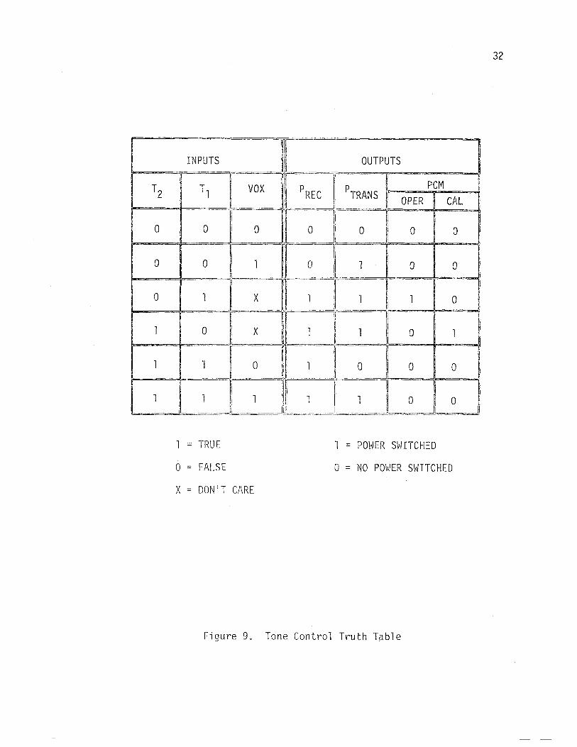
A modified version of the truth table in Figure 2 (Chapter II)
is given in Figure 9. The modification consists of combining the
astronaut interrupt instruction with the GBS interrupt instruction
(GBS control instruction word 11). The various commands and power
switching instructions are related logically to the digital
instructions T,? T2, and VOX by
PREC = T, + T2 (8)
PENe = 11T2 + T,12 (9)
PTRANS = (T1T2 + T1T2)VOX + 11T2 + T,T2 (10)
OPERATE ~ 1,T2 (11)
CALIBRATE = T,12 (12)
Equations 8 through 12 are implemented as shown in Figure 10, which
shows the complete schematic for the tone control logic and power switching
circuits. For certain power switching instructions, an inverter was
32
INPUTS i OUTPUTS -----',
T2 Tl VOX ~CJ PTRANS PCM
OPER CAL . L -·~-ll -
, 0 0 0 o I 0 0 0
I ~ ,
0 0 1 o L 1 0 0
1 [~ -
0 "'
X 1 0 . ..---J
I r 1-- 1 I
1 0 X 1 0 i I
1 ! 1 0 1 0 0 0
, ~ 1 1 i 1 I,!; 1 1 0 0 1 lUL.... - r:
1 = TRUE 1 = POWER SWITCHED
o = FALSE o = NO POWER SWITCHED
X = DON'T CARE
Figure 9. Tone Control Truth Table

Fig
ure
10.
Tone
Con
trol
L
ogic
S
chem
atic
.
HEP
52
HEP
50
Rec
eive
r
Pow
er
-5
+5
Enc
oder
Pow
er
-5
Cap
acit
ors
in
ufo
w
w

34
required since a logical 0 turns the transistor switch on.
A free running (astable) multivibrator with short duty cycle
operation (300 milliseconds ON and 2 seconds OFF) switches the receiver
transistor power switch on and off in the sampling mode. 15 An
interrupt input to this astable multivibrator is provided. A logical
zero at this input allows free running operation~ whereas a logical
1 (indication of tone signal transmitted) locks the receiver power on.
The transistor power switch uses both NPN and PNP transistors.
This type of switch is required because of split supply operation.
A logical 1 inhibits current flow to the respective subsystem. In
the OFF state, the voltage applied to the subsystem is at ground or
system common. A logical zero turns the transistors on and permits
power flow to the subsystem load. For proper operation of the tran
sistor switch, a diode is used at the input to clamp the logical 0
signal to approximately system common.
For safe operation of CMOS devices, the input signal must not 16 exceed the power supply voltage. However. if the control logic
is such that power is not switched to the PCM subsystem. excessive
input signal excursion due to the logical operate and calibrate
commands can occur. To circumvent this problem, a CMOS switch
was used to return OPERATE and CALIBRATE signals to system common
when no power is delivered to the PCM subsystem.
The VOX contro1 signal is generated using a peak detector and
voltage comparator following the astronaut's voice amplifier (Figure
11). The resulting signal operates a retriggerable one-shot

Volume Control From 200 +5 50 K Hz Band- Notch Control pass220
From PLL Detector
• 1
()--1 Astronaut
Microphone
Capacitors
=
270 K
in ufo
Figure 11.
K
=
To Tone Decoders
220 K +5
K
0022
= -5
+5
22 K
To Transmitter
27 K
-5
Portable Unit Audio Schematic.
35
Ea rphone
-5

36
multivibrator with a one-shot time constant of approximately 2 seconds.
This delay allows short pauses in voice signals while avoiding
transients caused by power switching. The astronaut1s voice amplifier
consists of two cascaded operational amplifier stages. A gain of 2000
;s required to amplify the small 1 millivolt microphone signal to one
of sufficiently high amplitude to modulate the transmitter and to
activate the VOX circuit. (A bone conduction microphone furnished
by NASA JSC was us~d in this work.) Both stages are coupled to avoid
DC offset at this high gain.
The 200 Hertz tone transmitted by GBS was originally assumed to
be inaudible~ but could actually be heard. To eliminate the tone, it
was notched out in the receiver audio stages. The use of a notch filter
requires a bandpass filter. To minimize the number of components~
the output of the 200 Hertz bandpass filter in the 200 Hertz tone
decoder was fed back to the audio stages (Figure 11). The second opera
tional amplifier in the audio stage is used as a phase inverter to
provide the proper phase relations for notch operation. The third
operational amplifier has variable gain and drives the headset worn
by the astronaut. The particular headset. provided by the NASA
Johnson Space Center~ was a low impedance type; consequently a current
limiting resistor was used in series with it. This limiting resistor
represents considerab1e signa1 10ss; however enough power was
delivered to the headset so that adequate volume resulted.

37
3. Transmitter
The first stage of the transmitter (Figure 12) consists of a
crystal oscillator which doubles as a direct FM modulator. Transistor
Q1 operates in a common base configuration. The tank circuit is
resonant at approximately the crystal frequency (4.444 MHz).
Around 30 percent of the output signal is fed back to the emitter to
sustain oscillations. The crystal~ together with the inductance
and capacitance in series with it~ acts as a series resonant bypass
el ement. Direct modu"j ati on is Behi eved by varying the bi as across
the varactor diode. A change of reverse bias across the varactor diode
causes the equivalent capacitance to change$ which subsequently causes
the series resonance of the bypass branch to change. Small, yet
adequate, deviation is possible with this circuit. The inductance in
series with the diode and the crystal tends to linearize the
capacitance-voltage characteristics of the varactor diode. 18
The output signal of the oscil1ator~modulator is fed to a phase
modulator. Phase modulation is obtained by adding two RF signals of
fixed phase difference and of varying amplitude. The signal from
the oscillator is applied to a phase splitting network. Two signa1s
are produced: one leads the oscillator signal by 45 degrees and the
other lags the oscillator phase by 45 degrees. In a push-pull type
of operation, these signals are amplitude modulated by the modulating
s;gnal. 17 When these two signals are added together, the resulting
signal is phase modulated. A graphical description of this procedure
is shown in Figure 13. This push-pull type of phase modulat"ion is

30 'f
h.
~'tBMHl.
I'
AU
DI0
.l
4.1
K
II'tP
UT
-r ,DO
l! -5
3.3
(,F
0-----
1 FR
OM
Sr
c.01'l
D
TRIP
LER
1,8
I(
.. 5
"5 1
2.,
h
POW
ER 0
&
~
CON
TRO
L IT
·0047
10
0 5
pF
_ 15K
>100
1'.
osc. \
LlA
TO
R/ M
OD
ULA
TOR
-5
PI
IASE
M
OD
ULA
TOR
peN
IN
PU
TS
O
UTP
UT
STAG
E
+5
~ Lr
1,,/11
1-
I <fh ~
r,O
DS
T
,001
-5
Ls
-5
2N51
79
12
.'2
PF
2N
SI79
2
2.)
':1
00
22
"Dl~
G8p
!' 2:
1 K
~J"fr
'--
----
_.
-
··5
F'ig
ure
12.
PoY
'Lab
le
Uni
t T
ran
smit
ter
Sch
emat
ic
FOW
OO
TFR
AM
'lfl
t.n
+5
+5
47pF
FIR
ST
TRIP
LE'R
SE
C.01
'lD
lRIP
\..E
R
All
R
esi
,sto
rs
tn
Ohm
s an
d A
ll
cap
acit
ors
in
M
icro
fara
ds
Un
less
O
ther
wis
e N
oted
.
Ll~
15
Co
il,
J.W
. M
l1le
r #
70
F1
55
AJ.
L2
: 10
A
dju
stab
le C
oil
, J.
W.
Mil
ler
1/47
AI0
6CP
C.
l3,L
4:
2.7
h
Ad
just
ab
le C
an
, J.
\>I.
Mil
ler
~46A
2.76
CPC.
LS.l
6:
0.5
6
h A
dju
stab
le
Co
il.
J.W
. M
1l1
er
1/46
A68
7CP
C.
L7
,L8
: 0
.2
h A
dju
sta
ble
C
oil
. J.
W.
Mil
ler
#4
8A
18
7m
pc.
38
TO O
UTP
UT
'jTA
(',E
27 p
f
MiO
WOU
'l' F'
RA~

No t"Jodul ati ng S-ignal
~ll= A
" " " r~ = A/2
/ G = 0 /
/
A + (j,
R = /2/142+6 2
39
G = Tan- l {MA}
Positive Modulating Signal
A - (j,
Negative Modulating Signal
Figure 130 Phasor Representation of Phase Modulationo

implemented using a matched pair of field effect transistors. FETs
are used because their high input impedance will not load the phase
splitting network. Each FET is amplitude modulated by applying
40
a modulating signal to the source. The signal applied to the source
of one FET is made 180 degrees out of phase with the signal modulating
the other FET so that push-pull operation can result. The drain
currents are added in the tank circuit which is common to both drain
terminals (Figure 12).
This implementation has two major advantages over single transis
tor phase modulators. One is that the available phase deviation is
greater; the second and more important advantage ;s that the resulting
phase modulated signal has considerably less amplitude variation.
This is important when frequency multipliers are used, since, when
frequency multipliers are operated Class C, they are very sensitive
l Ot d "t" 18 to amp 1 u e varla lons.
Transmitter power switching is achieved by a FET switch shunting
the phase modulator output circuit. This implementation was used
primarily to avoid delays caused by oscillator starting time. The
oscillator is thus in operation continuously. Other advantages of
this power switching scheme include:
1. no charging power surges are required from the voltage supply;
and
2. no DC power loss occurs across solid state switching elements.
The FET used is a N-channel depletion mode JFET. When a logical
1 (+5 v) is applied to the gate, the channel resistance is low and

41
therefore shorts the tuned circuit. Since the remaining part of the
transmitter is operated Class C, no power will flow to these circuits.
When a digital 0 (-5 v) ;s applied to the gate, the channel resistance
;s high and consequently will allow transmitter operation.
The first and second frequency triplers that follow the phase
modulator are very similar. The transistors are biased beyond cutoff
so that they operate Class C. The collector load consists of a double
tuned capacitively coupled circuit. 19 The double tuned circuits
were designed to be slightly under-coupled so that attenuation of
undesirable harmonics would be goodo The output of the double tuned
circuit was connected to the input of the next stage by means of a
small capacitor which functioned as both a coupling element and an
impedance matching element. A frequency doubler which produces the
80 MHz final RF frequency follows the second frequency tripler; the
output of the doubler is fed to a Class C amplifier which drives a
quarter wave antenna. The output amplifier is matched to the antenna
by a capacitive voltage divider. All individual stages comprising
the transmitter have power supply decoupling as shown in Figure 12.
4. PCM Encoder
The front end of the peM encoder consists of a switch network,
calibrate signal generator, and signal conditioners (Figure 14). The
switches preceding each signal conditioner are CMOS bilateral switches
connected in a double pole double throw (DPDT) configuration. The
switches are operated by OPERATE and CALIBRATE digital signals. An
OPERATE signal switches the differential inputs of the signal

43
conditioners to electrodes situated on the astronaut's body. A
CALIBRATE command connects the calibrated generator to the inputs of
the signal conditioners.
The calibrate signal generator is basically a CMOS astable
multivibrator set for approximately 5 Hz. A precision 1 mv
peak-to-peak differential signal is produced by the resistor divider
network and the Zener diode regulation. The extra inverters and the
dual resistor divider are used to cancel common mode voltages.
The signal conditioners each have gains of 1000 and are designed to
handle up to a ±2.5 mv differential input signal. DC offset voltages
are no problem with this circuit because of the AC coupling between
the buffer amplifiers and the differential amplifier. The use of large
values for the coupling capacitor and resistor in series with the
capacitor gives a low frequency cutoff of 0.03 Hz which is adequate
for most physiological signals. 9
Five of the seven instrumentation amplifiers are connected to a
multiplexer integrated circuit (l2~ see Figure 15). The multiplexer
consists of eight channel select decoders and eight select switches.
The channel select decoder is addressed by a word counter (Z6)' The
word counter also addresses additional CMOS switches (1/2 of lS) to
submultiplex the remaining two physiological channels. The remaining
multiplexer inputs are tied to system common corresponding to the zero
reference channel and frame synchronization period. The multiplexer
output is connected to the pulse width modulator. The pulse width
modulator consists of a sweep generator and voltage comparator (Z4).

o D
EN
OTE
S
CH
AN
NE
l_
INP
UT
'5
5 M
Hz •t--~
~J.-~
j ZJ~
' ~
, «
__
_ ~(!J
Fig
uY'e
'1
5.
peM
E
nco
de
r
FOLD
Olrl
' "FRA
IDJ
)
~f~_-=
~"!SI4!31211
(04
05
1
ZI
, ~'1-I::-L5
~I-, ---
CD 4
DJ5
MU
LTIP
LEX
ED
AN
ALO
G
INPU
T
TO
TRA
NS
MIT
TER
['~'-81iJ
-+ '---:--
-[-r 4~'
CD
+02
4 Z
6 L
-lj-
=' f'
lr--
c:;:
" +
--'
I -~
j++'-'
--
i
L ~ ~
----1"
""'-
'-'"
'' ' ~ -
--I I
I, I ,
=
I I L
II
+5
;::
:::)
; 1
10K
WOR
D 5~NCH
-G:~~Jll
=-~----r
~~-::,~· ':
, , CD
4-0
13
ll5
JJ
II 11
+_,0_
+ t
1 ~ I
_
_<
__
_ -'=
rJE
____ _
--[ L_
___.::
:.:.~ _
_
--.--=
+----~
' -I [-----
---1 'k-
",c-,~' ,.
c,-
,_.-
~';-:"
IL
;1"t
tt~_
_ L,
t+1
cn :;
-
~~-
, PC
M _
_ __
-
----
---
----::-
-~--=-~--=---=-=
=:.:-.:.-
flES
ISTO
RS
IN
O
HM
S
CA
PA
C 1
TOR
S
1 N
MIC
RO
FA
Ro\
05
SE
RIA
L S
HIF
Y
iN"'
IT n
{)T
'I'i
1 ,
'Ol'l>
A 11
1M
,.-<,
44

45
The sweep circuit is a constant current source which drives an
operational amplifier integrator. The sweep is clocked by the word
clock signal (Figure 16) by discharging the integrating capacitor Cr ,
The output of the voltage comparator ;s high until the sweep voltage
equals or exceeds the multiplexer output. The output of the voltage
comparator and the word clock are applied to a logical AND gate
(1/4 of Z14) resulting in a pulse width modulated (PWM) signal
(Figure 16).
The pulse width signal gates (1/4 of Z'4 and 1/4 of Zg) a 5 MHz
signal to a counter (Z15 and Z16)' The oscillator is a hybrid CMOS
crystal oscillator which has outputs of 5 MHz~ 2.5 MHz, and 1.25 MHz.
After the gated oscillator pulses are counted, the contents of the
counter are parallel jammed into a shift register (Z20 and Z21)' The
counter is then reset before the next gated signal is available. While
the next signal is being counted s the contents of the shift register
are shifted out serially to the transmitter. A timing diagram of the
various control signals during each word period is given in Figure 17.
These control signals are generated by the digital integrated circuits
ZlO through Z13s I 17 , and Z,S·
The serial data s together with the word synchronization data
(Figure 16) are combined to produce two PCM signals which differ by
180 degrees. It should be noted that there ;s a one word delay between
sampled data and the PCM word representing the sampled data. This
signal is applied to a low pass filter (cutoff at 2 KHz) and
subsequently to the push-pull inputs of the phase modulator on the

Pulse Width Comparator Output
\lJord and Frame Synch
Composite PCM Signal
fUll Compos ite peM Si gna 1
Figure 16. peM Encoder Timing Diagram
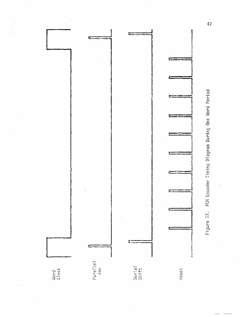
\lJor
d C
lock
Par
alle
l Ja
m
Ser
i a 1
Sh
ift
Res
et
J _
l
-~
~ -
~ ~
j l_
b ~,"
_~l_J
~ ~ __
_ Fi
gure
17.
pe
M E
ncod
er T
imin
g D
iagr
am D
urin
g On
e W
ord
Per
iod
..j:::>
"

48
transmitter board.
The PCM encoder shown in Figure 15 ;s the same as the one designed
by NASA Ames Research Center with two exceptions. The CMOS quad
NOR gate (Z23) was added to interface with the transmitter. The second
modification consisted of changing the synchronization format slightly
to be compatible with the decoder when connected by the "pseudo-indirect"
FM link. The original synching signal consisted of a one bit duration
negative word synch pulse between regular data words and a one word
duration negative pulse separating the individual frames. The high
pass response inherent with "pseudo-indirect" FM results in considerable
distortion in the long duration frame synch signal which causes
unsatisfactory operation of the decoder. ConsequentlY9 a one shot
mu1tivibrator (Z22) was incorporated in the encoder such that the word
synch pulse immediately preceding the frame synch slot would be skipped.
The skipped word synch pulse has the same effect as the original
format, so that no modifications of the decoder were required in
this respect.
C. Ground Based Station
The transmitter and receiver are commercial units and will not
be discussed here. A general description of the transmitter and receiver
is provided in the GBS description in Chapter II.
1. PCM Decoder
The PCM decoder is identical with the system that NASA Ames
Research Center designed to be compatible with the PCM encoder 9 with
one exception. The high pass response that resulted with
"pseudo-indirect" FM caused degraded performance of the decoder.

49
The degraded performance was a result of the difficulty involved in
determining digital levels. In consequence, additional wave shaping
circuits were required at the input of the decoder.
The transfer function of a first order high pass filter is
where w, is the low frequency cutoff.
Ideally, the transfer function describing the received signal
as a function of the encoder signal would be
H(s) = ~~- = l~
where E(s) and R(s) denote the encoder signal and received signal,
respectively. In other words~ the input signal and output signal
would be identical,
The desired transfer function would be obtained if the high
pass function (Equation 13) were cascaded to a transfer function
which exhibited the reciprocal response. That is, if the received
signal was operated on by the reciprocal high pass function.
Hhp-1(S) = (s + wll/s = 1 + w,/s.
the result would be
R(s) = s/(s + w,) . (s + w,)/s . E(s) = E(s).
(13 )
(14 )
(15 )
(16 )
50
The implementation of the transfer function given in Equation
15 is straightforward. The transfer function can be realized by an
integrator and adder stage. The integrating capacitor and input
resistor are chosen to provide the w, integrating constant. The
actual implementation can be realized using a single operational
amplifier configuration. 20
The response correcting network improved the waveshape of the
PCM data considerably but introduced an additional problem. The cir
cuit overemphasized the frame synch period component (590 Hz), resulting
in a relatively slow variation in the levels of the digital data.
Component values were adjusted in an attempt to reduce this effect
in the response correcting network, but no improvement could be obtained.
Additional signal processing was required to prevent this variation in
level from affecting the following voltage comparators. An envelope
detector was used to detect the undesirable variation; the output of
the envelope detector was then inverted and added back to the original
signal, resulting in cancellation of the undesirable component. This
procedure was chosen, rather than a notch filter, because no circuit
adjustments were requiredo
The compensated PCM signal is then fed to two voltage comparators
where NRZ data and synchronization data are separatedo One word of
NRZ data is loaded into a shift register (Z,) by ten clock pulses
produced by a CMOS astable multivibrator (Z3)o The CMOS astable
multivibrator is enabled by the preceding word synch pulse and is
held on for ten clock pulses by a 0 flip-flop (1/2 of Z4) which is in

turn reset by a bit counter (Z6A)' The reset pulse from the bit
counter also updates a channel select counter (Z6B)'
The tenth bit indication from the bit counter also clocks a
51
second D flip-flop connected as a toggle flip-flop (1/2 of Z4)' This
second flip-flop activates switches so that the next word will be loaded
into a second shift register (Z2)' While the second word is being
loaded into the second shift register, the first word is held by the
first shift register for a one word period and is converted to an
analog value by a high speed DAC. The resulting analog value is demul
tiplexed to the proper output amplifier by switches (Z7A and Z7S)
controlled by the channel select CDunter (Z6B)' At the end of the
second word periods the first shift register ;s cleared and is ready
to accept the next word. Meanwhile s the second shift register holds
the second word which is converted to an analog level and demultiplexed.
The timing diagram for the systems is shown in Figure 18. A complete
schematic of the peM decoder is given il1 Figure 19.
A skipped word synch pulse indicates a frame synch signal. A
frame synch separator generates a frame synch pulse essentially by
comparing time intervals between word synch pulses. Each word synch
pulse discharges capacitor Cs (Figure 19) to ground. Subsequently,
the capacitor charges toward a positive five volts through a 330 kohm
resistor. This voltage is compared against a positive DC voltage
by an operational amplifier used as a voltage comparator. If the
RsC s time constant is properly sets the capacitor voltage will exceed
the DC voltage only in the case of a skipped word synch pulse. When

.02f
~8
K I i
"'l'
f ~"
."""
""~112~
I~A'
_ 1
I
ENVE
LOPE
D
ETEC
.TO
R
FOLD
OUT
FRAM
E )
\IO\lO
C., ~H~
~RTH
RE
SIST
OR
S IN
n.
. 1-
-1 %
R
ESI
STO
R':.
C~PAC.\TORS
IN
",F
A
LL
NP
H
-'2.N.~5b5
AL
L
PN.\:
) -
2t-
04
25
0
UN
LE
SS
O
"TI;I
£RW
I5E
: N
OT
E D
B-\
1
POW
ER
SUPP
LY
53
A.H
A,L
Oo.
O
UT
PU
T
-5
-5
0'0
~:::
roLD
O,lr
l' :l~

the capacitor voltage exceeds the DC voltage 9 the voltage comparator
output will switch from a low voltage (-5 volts) to a high voltage
(+5 volts). This step voltage signal is then differentiated~
producing a short frame synch pulse. The frame synch pulse is used
to reset the channel selector counter (Z6B) and master control (Z4).
The submultiplexed channel is demultiplexed by use of a
54
counter and a reset scheme which closes the demultiplexing switch
every other frame count. To ensure that the desired submultiplexed
channel is being demultiplexed~ the two physiological channels are
required to have different peak values. The voltage comparator is
set to differentiate between the two peak values and to reset the
counter if the wrong channel is being submultiplexed. The fully
demultiplexed channels are filtered by an active low pass filter with
high frequency cutoff of approximately 100 Hertz.
2. Control Signal Generator and Audio Circuits.
The tone generatorg tone reeds g tone select logic and audio
stages in GBS are located on a Single board. A schematic of the control
circuits on this board is shown in Figure 20.
The audio portion of this board consists of a switch network, an
audio buffer preamplifier~ and an audio output stage (Figure 21). The
switch network is used to inhibit the signal to the following audio
stages when peM data are transmitted. The word synch output on the
decoder board (digital levels of +5 v and 0 v) is interfaced to the

-5 ~ 100
K
,
l+5
Sly
-5
.068
1/4
~~CD4016
'1/4
C04
016
Con
trol
Sw
itch
es
Fro
nt
Pane
l ! +1
5
~
H
1- -T
rans
mit
ter
ON
/OFF
Sv
Ji tc
h F
ront
Pan
el
Cap
acit
ors
in
ufo
Tra
nsm
i tte
r
Rep
co
Inc.
M
odel
810-
041
l ,1
Tone
Gen
erat
o R
epco
In
c.
#810
-024
-02
Voi
ce
Fig
ure
20.
GBS
Tone
Con
trol
Sc
hem
atic
200
Hz
Tone
R
eed
-w--
100
Hzrj I
Tone
c::
s
LED
Fro
nt
Pane
l
(J1
(J
1

33
K
From
G
BS
i 1
/4
Rec
eive
r
10
K
From
TP.2
33
CD
4016
-5
-5
-5
All
Cap
acit
ors
in
ufo
unle
ss
othe
rwis
e no
ted.
+
8
3
18:. : =
1
=
Ast
rona
ut
Mic
roph
one
Fig
ure
21.
GBS
Aud
io
Sch
emat
ic.
10
K
10
K
8 oh
m
Spea
ker
=
Ul
0"1

57
CMOS circuitry (digital voltage levels of -5 v and +5 v) using a
voltage comparators and then fed to a retriggerable one shot multiv;
brator. The output of the one shot is used to control the audio switch.
When the PCM signal is presents the switch is opened so that the
undesired signal will not be heard over the speaker. When the PCM
signal is terminated~ the switch will close and allow voice signals
to be heard. The buffer preamplifier is an operational amplifier
connected in a voltage controlled voltage source configuration and
has a gain of three. The audio output stage is a linear integrated
circuit, one watt, audio amplifier driving a 0.5 watt, 8 ohm speaker.
The audio amplifier is connected according to the application
information supplied with the Motorola HEP C6004 integrated circuit.
The tone control circuitry consists primarily of an astable
multivibrator with a frequency of 1 Hzo Various inhibit and enable
signals originating from the tone select switches are provided.
When switch S, is set for a logical 1 (+5 V), it inhibits multivibrator
operation and allows one tone to be selected. With Sl set in the
inhibit position. switch S2 determines which of the two tones will be
activated. With switch S, set in a logical 0 position (ground poten
tial), the astable multivibrator is allowed to operate. Because of
the conditional connection of 52 to 5" 52 has no control in this
mode.
A delayed indication of GBS transmitter power is provided on
this board. The purpose of this indication ;s to inform the GBS con
troller that enough time has elapsed since the activation of tone trans
mission for the receiver in the portable unit to be locked on. The

58
circuit essentially measures capacitor charging time. When the
capacitor voltage reaches the CMOS transmission level, an LED on the
GBS front panel is turned on. The delay between initial tone trans
mission and LED indication is about 3 sec.
A microphone buffer stage is provided on this board. The circuit
is used as an impedance converter so that the 1 megohm microphone
source is matched to the 5 kohm input impedance of the transmitter.
A voltage divider was used to reduce the microphone signal to the proper
level required by the transmitter (7 mv RMS for full modulation).

CHAPTER IV
DISCUSSION OF RESULTS
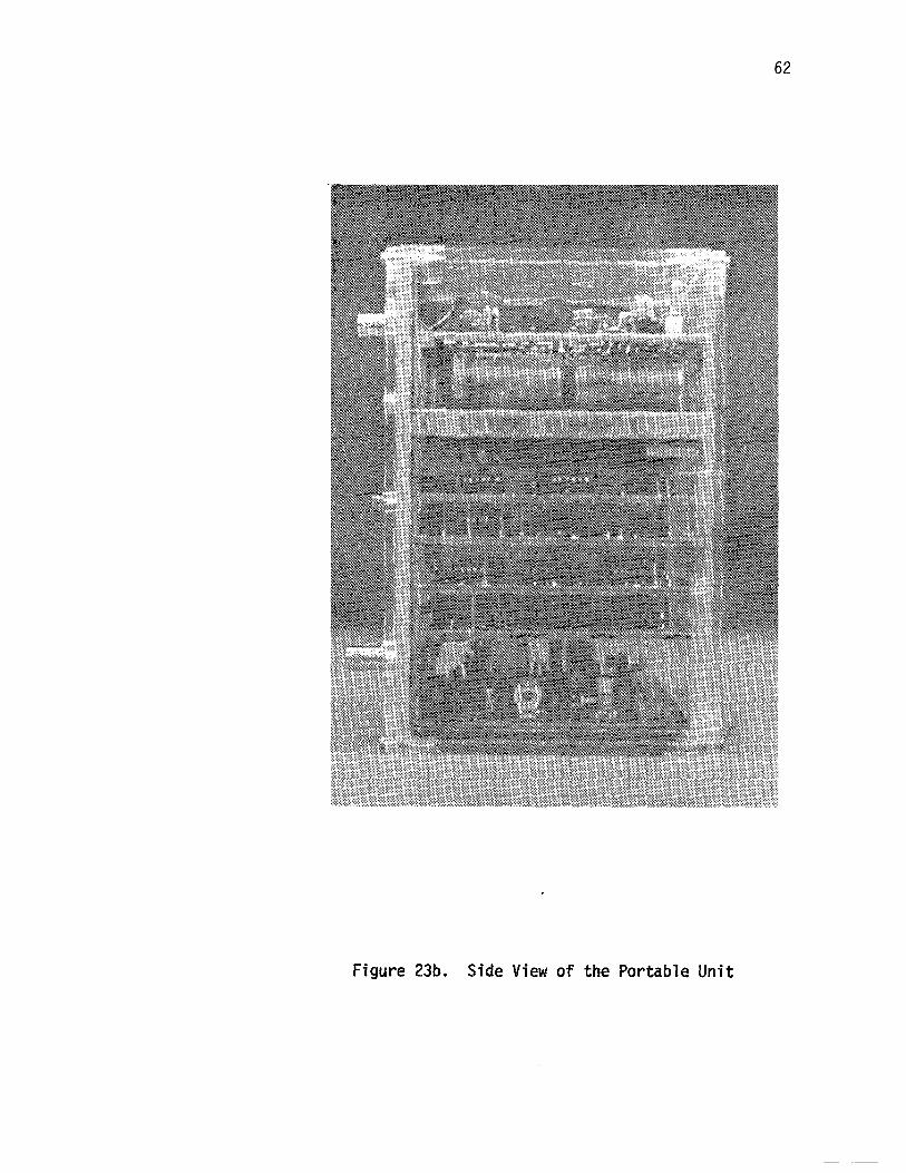
The GBS unit and the portable unit are shown in Figures 22 and
23, respectively. The system operates within the specifications
established by NASA JSC. For the complexity of the system, the power
requirement of the portable unit is quite low. A number of techniques
for improving system performance became apparent in the last stages
of design and subsequent testing; these modifications are presented
as suggestions in this chapter.
A. Resul ts
The system was designed to have the capability for seven channels
of physiological data. However~ only three channels of ECG data were
used in testing. Other physiological data, such as temperature and
respiration. were not used because of the requirement of additional
signal conditioning. Such signal conditioning can be incorporated into
the system, but was not required in the specifications.
An illustration of a typical signal generated by the PCM encoder
is shown in Figure 24(a). The peM signal received by the GBS receiver
is shown in Figure 24(b). The high pass response indicated by the
received signal is a result of the IIpseudo-indirectli FM format. The
output of the response correcting network is shown in Figure 24(c).
A noticeable improvement in noise margin is exhibited by this signal.
Strip charts of three channels of ECG data are shown in Figure
25(a). These are compared to the signal at the output of the signal
59

60
N N
QJ S::s C'I .~
u..

61
Figure 23a. Front View of the Portable Unit
62
Figure 23b. Side View of the Portable Unit

63
a.
b.
r J c.
Figure 24. PCM Signals: a. Output of PCM encoder b. Received at GBS c. Delivered by the compensating network

64
I: f~~: :'1; :T~ ::': m~ :~: ~m~t ~jLi}:H:; fiif:Li:'~ltH:;:H~tj-t iH l!: i i: I I':; ilH~ : :1-11: ~lJlnH-HUmt :':'~I! iii' ,. ":+ii ;tlfIH;#fU~-i·::rflbTr, ifft81rntrJH il:! ii: ti::iill!::l,'.:~li!: jd [if;
il! :h: :,1;i; 'iii ~;Him ii\:.'!' :'fc;F(j1tIITf1mfE1WHi'!::: IH;I!:t:::! It lilit:'l iiii :;,,';1 iiiii" :ii)~!li!:t Fi' irHHiiin ii; i!:i! 11 i' i,; Ji!i :!:::; 1/71; :~!!ii:
: : /:ii i' : ,'i; ii' liM :~U :i!'l :t;? 'Xi: ii: ill 'l/:ii :::i l ", H,j. i:' !1:::I!
'i',I! li:i i:; P :; :, :t: if 'ni':" Ii:, '/'1 :,,':1: iii Uti :: Ii': 'iii i: ii:'i: ',:.: :/11 If' ';:. ::n iiii;; ,I: ::i:U~;Li! + iii, Iii; !.;: fL: : ii iii!!!:: :iIi it ;t~l :]ir.P: ( ::1. ,t:li:. i'" ,., :f',,:l' :': ii:' • 'i ijili ",1:': H If II lUi !th ,t .;1; :;ii'j: :'1::' :,I,,:d::[: ,:1:: if: ': ':,:::;::Yni '1H n:1 ::i':f~l~mrTi;' ····t~ ~ .• :' I~" ":. , .• :.: 'i! !!: ,:tt·:!-.lLH!llH:UJl
Lead I
Lead II
Lead III
Figure 25a. Decoded Telemetry ECG Data Horizontal Scale: 25 mm per sec; Vertical Scale: 200 mv per mm

65
conditioners in the portable unit (Figure 25(b). High quality repro
duction of the heart wave is noted.
The ranges of the system1s RF links are adequate. Reliable trans
mission of both PCM signal and voice is achieved at a distance of 100
ft from GBS. Further range can be demonstrated; however the received
signal becomes somewhat noisy at greater distances.
When all subsystems of the portable unit are activated, a total
current drain of 65 ma is required of the battery source. The
batteries used are rated at a capacity of 1.2 ampere-hours. This
capacity corresponds to 20 hours of continuous operation before a
battern recharge is required. In actual use, however, the battery
life will be greater since subsystems will not be required continuously.
B. Proposed Modifications
The problems encountered with the portable unit's transmitter
are basic ones. The combined specifications of crystal control and
wide deviations required by the peM data signal are mutually
exclusive. The use of a "pseudo-indirectll FM system increased
deviation but caused loss of valuable low frequency information.
Transients caused by the high pass filter response are very random
in nature, that is, the voltage spikes and voltage droop discharge
times vary with the changing position and duration of the NRZ data
(Figure 25). The resulting effect is a decrease in the noise margin
of the PCM digital Signal. For a digital signal, the noise margin is
defined as the difference in the lowest voltage representing a logical
1 and the highest voltage representing a logical O. To circumvent

Lead I
Lead I II
Figure 25b, Transmitted Telemetry ECG Data Horizontal Scale: 25 mm per sec; Vertical Scale: 100 mv per mm
66

67
this problem, additional waveshaping circuits were used (see Chapter
III).
Ultimately, the best approach to solve the wide bandwidth problem
would be a redesign of the transmitter and possibly a change in the
modulation. Simultaneous transmission of astronaut's voice and PCM
data should be included in such a redesign.
The problems associated with simultaneous transmission of voice
and PCM data have been discussed previously. The resulting frequency
spectrum of the RF signal must consist of two separated RF spectra.
Implementation of such a scheme requires essentially two separate
transmitters which possibly would be matched to a single antenna
by use of a directional coupler. Two transmitters cause increased
power consumption and size; consequently~ a re-evaluation of the
design approach and of the operating specifications of the transmitter
must be made.
The redesign of the transmitter includes
1. low power consumption;
2. small size;
3. reduced number of RF coils for hybridization purposes; and
4. a solution of the bandwidth problems associated with PCM data.
To keep size and power consumption down, at least one of the two
separate transmitters must be simplified. This simplification must
be implemented while causing no degradation in the modulation
characteristics.
One approach to the redesign would be to use a different modulation
format. One very efficient modulation scheme would be pulse modulation

68
(PM). In this format, the RF carrier is switched on and off by the
modulating digital signal. The exact implementation of a PM trans
mitter for this, application would require additional research. Trans
mitter power switching or oscillator switching would exhibit inadequate
response to the high bit rate peM data. A better approach would be to
use an FET switch shunting a tank circuit of some stage following
the oscillator. An alternate approach would be to modulate the emitter
voltage of a common emitter class C stage. This would in effect allow
class C operation during a low digital modulation signal and inhibit
operation at the high digital modulation signal. A PM transmitter of
good output power and efficiency could be realized using only three
stages: a first stage consisting of crystal controlled oscillator
operated at 60 - 70 MHz~ a second stage consisting of a frequency
doubler with PM modulation 9 and a final output stage operating at
120 - 140 MHz. Modification of the present peM tri-state logic to
two stage logic would be reqtrlred for P~1 transmission.
A two state peM signal would require a code sequence in place
of the present negative synch pulses. To maintain present bit rates,
word synch information must be eliminated. This would require the PCM
decoder to be able to remain in synchronization with the PCM data for
one entire frame period. While this reduction of synchronization
information increases the probability of the decoder falling out of
synchronization, reliable operation can be realized by using a somev,!nat
more sophisticated decoder synchronization scheme. The frequency of
the bit clock which synchronizes with the incoming peM data can be

69
matched very closely to the crystal controlled peM bit rate by use of
crystal control in the decoder, A frequency tolerance of .01 percent
is easily achieved with crystal oscillators and this precision is
more than adequate to maintain synchronization for one frame period.
Any small difference between peM bit rate and the bit clock frequency
would be corrected by turning the bit clock off for a few cycles
during the frame synch word period and restarting it at the proper
time to synchronize with the next frame period.
The code used in the frame synch word period would have to
be such that it could not be mistaken for a regular data word. In
the present peM encoder implementation~ the maximum binary number
representing a data word is 1111000000 (960 in decimal). By using
a sequence of ten consecutive ls as the synchronization code, the
decoder could recognize this sequence and subsequently induce synchronous
operation. A recognition of this code by a sequence detector could
be used to turn off the bit clock. Following this code~ a less
elaborate code would be required to restart the bit clock for the next
frame. This bit clock enable code is conditiona1 on the frame code
sequence immediately preceding it9 and therefore can be any convenient
combination of 1s and Os. It should be noted that Os separate each
word in the frame, thus preventing the possibility of a false detection
of a frame synch code.
The sequence detector would be implemented using four flip-flops
and appropriate combinational logic. A design procedure for this
implementation can be found in the literature describing digital

. 't 21 ClrCUl S.
The second transmitter used for voice transmission could be
either an AM or an FM transmitter, An AM transmitter would allow a
70
simpler implementation; however, more knowledge of the space environment
is needed to determine if the more noise sensitive AM RF signal would
give satisfactory results, Assuming an FM transmitter is used for
astronaut voice communication, a simpler implementation than the present
transmitter must be made. A direct FM scheme incorporating a phase
locked loop frequency multiplier would reduce size and the number of
RF coils; however 9 no appreciable amount of power would be saved. A
regular Class C multiplier stage would be required following the out-
put of the PLL multipliers since the upper operating frequency of most
PLLs are around 30 MHz.13
An additional improvement that could be made is a modification of
the control subsystem. At present. continuous transmission of control
tones, and consequently, continuous operation of the receiver in the
portable unit, is required for GBS control, If, instead, a control code
were generated such that the receiver would lock for only the time
required to receive and properly decode the control information,
receiver power consumption would be reduced, In this mode, the receiver
would have to sample occasionally to check instruction status.
The modifications listed above would give increased performance
over the present system. Power requirements probably would increase
due to the extra transmitter required in the portable unit; however,
the current drain should not be greater than 100 ma. The physical

size of the total portable unit can be reduced considerably by
hybridization. It must be noted, however, that portions of the
RF circuits are not simply hybridized because of the required RF
coils and the higher frequencies involved; possibly gyration or
high frequency PLLs could be used for this purpose.
71

CHAPTER V
CONCLUSION
A seven channel physiological telemetry system was designed,
constructed, and tested. Three ECG leads were monitored simulta
neously, and two-way voice communication was achieved. The portable
unit operated properly under GBS transponder control.
The major design problem was associated with the constraints of
a wide bandwidth FM transmitter with crystal control. The tri-state
logic format used by the NASA Ames Research Center also compounded
this difficulty. However, by using an I!indirect FW scheme and
incorporating additional waveshaping circuits at GBS, proper operation
of the system was obtained.
In the present form, the telemetry system has capability for
seven channels of low level (2.5 mv peak maximum) physiological
signals with bandwidth between 0.03 Hz and 100 Hz. Additional signal
conditioning and modification of the instrumentation amplifiers gains
are required for other signals.
72

REFERENCES
1. Nichols, Myron H. and Rauch~ Lawrence L'9 Radio Telemetry. John Wi1ey and Sons, Inc., New York~ 1954.
2. Caceres~ Cesar A.s Biomedical Telemetry. Academic Press~ New York and london. 1965.
3. Johnston, LB., "Two Way Telemetry for Hospital Use", International Telemetry Conference Proceedings, 1965.
4. Rase, Kenneth D., "Telemetry Physiological Data from Athletes", International Telemetry Conference Proceedings, 1965.
5. Fryer, Thomas B., Implantable Biotelemetry Systems, NAS SP-5094, Office of Technology Utilization, National Aeronautics and Space Administration, Washington, DC, 1970.
6. Javid, Mansour and Brenner, Egon, Analysis and Transmission and Filtering of Signals~ McGraw Hill, New York, 1963.
7. COS/MaS Digital Integrated Circuits, RCA Corporation, Solid State Division, Somerville, N.J., 1974.
8. Vander Kooi, Marvin 1(', Ll44 Programmable Micro-Power Triple OP Amp, Application Note~ Si1iconix, Inc., December 9 1973.
9. Wood, Gary B" A Digital Ph.ysiological Spectrum Analyzer~ Masterls Thesis, Texas Tech UniversitY9 Mai~ "1973,
10, Carlson, F,M.~ Application Considerations for the RCA 3N128 VHF MaS Field=Effect Transistor, Application Note AN-3193, RCA Solid State Division~ 1973.
11, Palenschat s Fred~ "Design RF Oscillatorsll~ Electronic Design, Sept. 27~ 1974.
12, Carlson, F.M.~ VHF Mixer Design Using the RCA 3N 128 MOS Transistor, Application Note AN-3341, RCA Solid State Division, 1973.
13. Monolithic Phase-Locked Loop, XR-215 Data Sheet, EXAR Integrated Systems, Inc., October, 1973.
14. Monolithic Tone Decoder~ XR-S67 Data Sheet, EXAR IntegY'ated Systems, Inc" October, 1973,
73

74
15. Dean, J.A. and Rupley, J.P'9 Astable and Monostable Oscillators Using RCA CMOS/MOS Digital Integrated Circuits. Application Note ICAN-6267~ RCA Solid State Division~ 1974.
16. Painter, R.R'9 Gate-Oxide Protection Circuit in RCA COS/MOS Digital Integrated Circuits, Application Note ICAN-6218, RCA Solid State Division, 1974.
17. Dawley. R.L'9 editor, The Radio Handbook, Editors and Engineers, LTD., Santa Barbara, CA, 1947.
18. Noble, Frank W., IIVariable Frequency Crystal Oscillators ll,
Proceedings of the IEEE, December. 1966.
19. Stewart, Harry E'9 Engineering Electronics, Allyn and Bacon, Inc., Boston, Mass., 1969.
20. Graeme, Jerald G .• Application of Operational Amplifiers, McGraw-Hill Book Company, New York. NY, 1973.
21. Kohavi, Zvi, Switching and Finite Automata Theory, McGraw-Hill Book Company. New York, NY, 1970.

APPENDIX A
OPERATING PROCEDURE
Once the system has been properly adjusted~ the operating procedure
is straightforward. Except for the astronaut interrupt control, which
consists of a spring loaded switch, the portable unit is automatic
and requires no control for proper operation.
The DATA input9 MIC (microphone) input9 and BATT (battery) input
are all keyed connectors. To operate the system~ a shorting plug is
connected to the BATT input. This plug connects the batteries to the
electronic circuits. In order to recharge the batteries. the plug
must be removed and a two-lead recharge cab1e connected. permitting
external access. The batteries should be charged at a constant 100 rna
rate for 16 hours for full charge.
The operating procedures for the GBS unit are more involved~ but
also straightforward. Initiallys all offset controls should be set
at a mid-point (500 on the dial). The SUBCOM channel selector switch
determines which submultiplexed channel is decommutated and -filtered.
The ON/OFF switch9 located in the lower left-hand corner of the
panel~ switches power to the GBS unit. A neon lamp, to the right
of the ON/OFF switchs indicates povller status. The microphone input
jack is directly to the right of the neon lamp. The microphone itself
has a push-to-talk switch; however s voice transmission will not take
place unless the transmitter p01fJer switch ; sin the ON pos iti on.
The transmitter power switch is in the upper left hand corner of the
panel, directly above the ON/OFF power switch. Activation of this
75

76
switch causes an RF signal~ modulated by one or both control signals~
to be transmitted. Three seconds after transmitter power has been
switched on 9 a red LED indicator 9 located above the transmitter
power switch, turns on and indicates enough time has elapsed for the
portable unit receiver to be locked up. Two switches (S, and S2)9
to the right of the transmitter switch~ select which control instruc
tion will be transmitted. Switch 51! directly to the right of the
transmitter power switch s inhibits and enables peM operation. In
the PCM inhibit position (switch S, in the up position), switch 52
(directly to the right of 51) has no control. When switch S, is in
the PCM enable positions switch S2 selects either a CALIBRATE or
OPERATE control instruction. In any combination of control switch
positions s GBS voice transmission is obtained.
The speaker volume control is located below the speaker. When
the PCM ENABLE switch is in the ENABLE position. no signal will be
delivered to the speaker.
For proper operations the GBS receiver signal level should be
set to give at least a 2.5 volt peak-to-peak peM signal.

APPENDIX B
MAINTENANCE
77
For proper operation of the systems a number of adjustments must
be correctly made. These adjustments include transmitter and receiver
alignment, tone decoder frequency adjustments~ and PCM decoder
adjustments.
The portable unit transmitter is aligned by successively tuning
each stage, beginning with the phase modulator tank circuit. All
stages except the final tripler stage are tuned by varying the slug
position in the appropriate coils. A locking insert is provided to
maintain slug position. The circuits are tuned to provide a maximum
DC voltage at the transistor emitter connection in the final stage.
The output tuned circuit can be tuned by using an RF power meter or
spectrum analyzers to provide maximum signal at 80 MHz.
The receiver alignment procedure consists of successively tuning
each stage beginning with the RF amplifier. With the GBS transmitter
on, each stage is tuned to give maximum 455 KHz signal at the
phase-lacked-loop detector input. The phase-locked-loop detector
has center frequency adjustment. A 2 kohm potentiometer is provided
for this purpose. While monitoring the PLL detector output (pin 8).
the potentiometer should be varied until the DC level ;s zero volts
with respect to system common.
The tone decoder center frequencies are adjusted by means of
20 kohm potentiometers. These potentiometers are conveniently
located facing the rear panel of the portable unit. The 200 Hz center

78
frequency control is located to the extreme right. A 50 kohm
potentiometer, directly to the left of the 200 Hz frequency adjustment
potentiometer, is used for adjusting the amount of 200 Hz signal fed
back to the audio stages for 200 Hz notch operation. With a 200 Hz
tone transmitted by GBS transmitter, the 200 Hz bandpass output should
be adjusted for maximum signal. The notch adjustment should be made
for minimum 200 Hz signal at the audio output stage, which drives
the headset. Similarly, the 100 Hz tone decoder is adjusted for
maximum 100 Hz bandpass output with a 100 Hz tone transmitted by
GBS. The 100 Hz adjustment potentiometer is located to the extreme
left on the same board as the 200 Hz adjustment potentiometer.
The adjustments on the decoder board in the GBS unit consist
of a DC offset control on the input amplifier and a bit frequency
control potentiometer. The DC offset potentiometer is accessible
from the rear panel of the GBS unit. The wave form monitored at
TP.l (Figure 18) should be such that the 0 digital level (tri-state
logic format) is at ground potential. The bit frequency which
synchronizes with incoming data is adjusted by means of a 20 kohm
potentiometer. Proper operation is obtained if the frequency is set
to within 10 percent of the incoming data rate. The adjustment is
made by monitoring the signal at test point TP.8. For proper align
ment, the bit pulses should be 19.2 ~sec apart.

79
APPENDIX C
PORTABLE UNIT INPUT CONNECTORS
The battery connector (BATT) and microphone/headset interrupt
connector (MIC) are Cannon Type ME 95185-2 connectors. The pin
connecting configuration is described in the following tables.
Pin Number
2
3
4
5
6
7
Pin Number
1
2
3
4
5
6
7
BATTERY INPUT CONNECTOR
Circuit Connection
Positive Battery Supply
Positive Circuit Connection
N. C.
Negative Circuit Connection
N. C.
Negative Battery Supp1y
N. C.
MICROPHONE INPUT CONNECTOR
Circuit Connection
Ground
Microphone
V+
Interrupt
Headset
Ground
N. C.

The DATA input connector is an Amphenol Tiny Tim 223-6
connector. The circuit connections are shown in the table below,
DATA INPUT CONNECTOR
Pin Number Circuit Connection
1 Channel D Differential Input
2 Channel D Differential Input
3 Ground
4 Channel H Differential Input
5 Channel H Differential Input
6 Channel G Differential Input
7 Channel G Differential Input
8 Channel F Differential Input
9 Channel F Differenti a 1 Input
10 Ground
11 Channel B Differential Input
12 Channel B Differential Input
13 Channel C Differential Input
14 Channel C Differential Input
15 Channel E Differential Input
16 Channel E Differential Input
17 Ground
80


![Copyright c 2007 Pegasys Inc,All rights reserved. · Linear PCM Dolby Digital [Mono/Stereo] PEGASYS Dolby Digital Encoder SDK Encoder DATA DATA DATA Dolby](https://img.dokumen.tips/doc/110x75/5d676a0d88c993d5408b7516/copyright-c-2007-pegasys-incall-rights-linear-pcm-dolby-digital-monostereo.jpg)