Embed Size (px)
Citation preview

appl
icat
ion
Wireless Test Solutions
Testing andTroubleshooting Digital RF CommunicationsTransmitter Designs
Application Note 1313
I
Q

The demand for ubiquitous wireless communications is challenging the physical constraints placed upon current wireless communications systems.In addition, wireless customers expect wireline quality from their serviceproviders. Service providers have invested a lot in a very limited slice of theradio spectrum. Consequently, network equipment manufacturers must produce wireless systems that can be quickly deployed and provide bandwidth-efficient communications.
At early stages of equipment design, rigorous testing is performed to ensuresystem interoperability. The increasingly complex nature of digital modulationis placing additional pressure on design teams, already faced with tight project deadlines. Not only must the designer test to conformance; he must also quickly infer possible problem causes from measurement results.
The objective of this application note is to help you understand why the different transmitter tests are important and how they identify the most common impairments in transmitter designs.
The application note focuses on cellular communications transmitters,although some of the measurements and problems described may also applyto other digital communications systems.
This application note covers the following topics:
1.How digital communications transmitters work.2.How to test transmitters and what test equipment characteristics
are important.3.The common impairments of a transmitter and how to
troubleshoot them.
The following information is also included as reference material:
• A detailed troubleshooting procedure (Appendix A).• A table of instrument capabilities (Appendix B).• A glossary of terms.• A list of reference literature.
2
Introduction

The first two chapters in the application note, covering topics 1 and 2, are targeted at new R&D engineers who have a basic knowledge of digitalcommunications systems. The third chapter is targeted at R&D engineerswith some experience in testing digital communications transmitter designs.For basic information on digital modulation techniques—essential backgroundfor this application note—please refer to:
Digital Modulation in Communications Systems—
An Introduction [1].
The measurements and problems described apply to most wireless communications systems. Some measurements specific to common technologies or standards are also mentioned. For more detailed information on CDMA and GSM measurements, please refer to:
Understanding CDMA Measurements for Base Stations
and Their Components [2]
Understanding GSM Transmitter Measurements for
Base Transceiver Stations and Mobile Stations [3].
Understanding PDC and NADC Transmitter Measurements
for Base Transceiver Stations and Mobile Stations [4].
Although this application note includes some references to digital communications receivers, it does not cover measurements and possibleimpairments of receivers. For more information on digital communicationsreceivers, please refer to:
Testing and Troubleshooting Digital RF Communications
Receiver Designs [5].
Note: The above application notes can be downloaded from the Web at the following URL and printed locally:
http://www.tmo.hp.com/tmo/Notes/English/index.html
3

1. Wireless Digital Communications Systems . . . . . . . . . . . . . . . . . . . 6
1.1 Digital communications transmitter. . . . . . . . . . . . . . . . . . . . . . . . 61.1.1 Analog I/Q modulator versus digital IF . . . . . . . . . . . . . 71.1.2 Other implementations . . . . . . . . . . . . . . . . . . . . . . . . . 8
1.2 Digital communications receiver . . . . . . . . . . . . . . . . . . . . . . . . . . 8
2. Testing Transmitter Designs . . . . . . . . . . . . . . . . . . . . . . . . . . . . . . . 9
2.1 Measurement model . . . . . . . . . . . . . . . . . . . . . . . . . . . . . . . . . . . . 92.2 Measurement domains . . . . . . . . . . . . . . . . . . . . . . . . . . . . . . . . . 10
2.2.1 Time domain . . . . . . . . . . . . . . . . . . . . . . . . . . . . . . . . . 102.2.2 Frequency domain . . . . . . . . . . . . . . . . . . . . . . . . . . . . 102.2.3 Modulation domain. . . . . . . . . . . . . . . . . . . . . . . . . . . . 11
2.3 In-band measurements . . . . . . . . . . . . . . . . . . . . . . . . . . . . . . . . . 122.3.1 In-channel measurements . . . . . . . . . . . . . . . . . . . . . . 12
2.3.1.1 Channel bandwidth . . . . . . . . . . . . . . . . . . . . . . . 122.3.1.2 Carrier frequency . . . . . . . . . . . . . . . . . . . . . . . . . 122.3.1.3 Channel power . . . . . . . . . . . . . . . . . . . . . . . . . . . 132.3.1.4 Occupied bandwidth . . . . . . . . . . . . . . . . . . . . . . 142.3.1.5 Peak-to-average power ratio and CCDF curves . 142.3.1.6 Timing measurements . . . . . . . . . . . . . . . . . . . . . 162.3.1.7 Modulation quality measurements . . . . . . . . . . . 17
2.3.1.7.1 Error Vector Magnitude (EVM). . . . . . . . . . 172.3.1.7.2 I/Q offset . . . . . . . . . . . . . . . . . . . . . . . . . . . . 202.3.1.7.3 Phase and frequency errors. . . . . . . . . . . . . 202.3.1.7.4 Frequency response and group delay . . . . . 212.3.1.7.5 Rho . . . . . . . . . . . . . . . . . . . . . . . . . . . . . . . . 222.3.1.7.6 Code-domain power . . . . . . . . . . . . . . . . . . . 22
2.3.2 Out-of-channel measurements . . . . . . . . . . . . . . . . . . 232.3.2.1 Adjacent Channel Power Ratio (ACPR) . . . . . . . 232.3.2.2 Spurious . . . . . . . . . . . . . . . . . . . . . . . . . . . . . . . . 25
2.4 Out of-band measurements . . . . . . . . . . . . . . . . . . . . . . . . . . . . . 252.4.1 Spurious and harmonics. . . . . . . . . . . . . . . . . . . . . . . . 25
2.5 Best practices in conducting transmitter performance tests . . . 26
4
Table of Contents

3. Troubleshooting Transmitter Designs . . . . . . . . . . . . . . . . . . . . . . 27
3.1 Troubleshooting procedure . . . . . . . . . . . . . . . . . . . . . . . . . . . . . 273.2 Impairments. . . . . . . . . . . . . . . . . . . . . . . . . . . . . . . . . . . . . . . . . . 28
3.2.1 Compression . . . . . . . . . . . . . . . . . . . . . . . . . . . . . . . . . 293.2.2 I/Q impairments . . . . . . . . . . . . . . . . . . . . . . . . . . . . . . 323.2.3 Incorrect symbol rate. . . . . . . . . . . . . . . . . . . . . . . . . . 373.2.4 Wrong filter coefficients and incorrect windowing . . 393.2.5 Incorrect interpolation. . . . . . . . . . . . . . . . . . . . . . . . . 423.2.6 Filter tilt or ripple. . . . . . . . . . . . . . . . . . . . . . . . . . . . . 463.2.7 LO instability . . . . . . . . . . . . . . . . . . . . . . . . . . . . . . . . 483.2.8 Interfering tone . . . . . . . . . . . . . . . . . . . . . . . . . . . . . . 513.2.9 AM-PM conversion . . . . . . . . . . . . . . . . . . . . . . . . . . . . 523.2.10 DSP and DAC impairments . . . . . . . . . . . . . . . . . . . . 543.2.11 Burst-shaping impairments . . . . . . . . . . . . . . . . . . . . 58
4. Summary . . . . . . . . . . . . . . . . . . . . . . . . . . . . . . . . . . . . . . . . . . . . . . 60
Appendix A: Detailed Troubleshooting Procedure. . . . . . . . . . . . . 61
Appendix B: Instrument Capabilities . . . . . . . . . . . . . . . . . . . . . . . 62
5. Glossary . . . . . . . . . . . . . . . . . . . . . . . . . . . . . . . . . . . . . . . . . . . . . . 63
6. References . . . . . . . . . . . . . . . . . . . . . . . . . . . . . . . . . . . . . . . . . . . . 64
7. Related Literature . . . . . . . . . . . . . . . . . . . . . . . . . . . . . . . . . . . . . . 64
5

6
The performance of a wireless communications system depends on the transmitter, the receiver and the air interface over which the communicationstake place. This chapter shows how a digital communications transmitter worksand discusses the most common variations of transmitters. Finally, it brieflydescribes how the complementary digital communications receiver works.
Figure 1 shows a simplified block diagram of a digital communications transmitter that uses I/Q modulation. I/Q modulators are commonly used inhigh-performance transmitters.
This application note focuses on the highlighted section of Figure 1.Measurements and common impairments for this section of the transmitterwill be described in the following chapters. Previous stages in the transmitterinclude speech coding (assuming voice transmission), channel coding, andinterleaving. Speech coding quantizes the analog signal and converts it intodigital data. It also applies compression to minimize the data rate andincrease spectral efficiency. Channel coding and interleaving are commontechniques that provide protection from errors. The data is also processedand organized into frames. The frame structure depends on the specific system or standard followed.
The symbol encoder translates the serial bit stream into the appropriate I andQ baseband signals, corresponding to the symbol mapping on the I/Q planefor the specific system. An important part of the encoder is the symbol clock,which defines the frequency and exact timing of the transmission of the individual symbols.
Once the I and Q baseband signals have been generated, they are filtered.Filtering slows the fast transitions between states, thereby limiting the frequency spectrum. The correct filter must be used to minimize intersymbolinterference (ISI). Nyquist filters are a special class of filters that minimizeISI while limiting the spectrum. In order to improve the overall performanceof the system, filtering is often shared between the transmitter and thereceiver. In that case, the filters must be compatible and correctly implemented in each to minimize ISI.
1.1 Digital communications
transmitter
1. Wireless DigitalCommunicationsSytems
SymbolEncoder
SpeechCoding
Channel Coding/Interleaving/Processing
RF LO
UpconverterBaseband
Filters IF FilterI
Q
I/QModulator
Digital Data
IF LO
I
Q
Amplifier
Power Control
Figure 1.Block diagram
of a digital communications
transmitter
The filtered I and Q baseband signals are fed into the I/Q modulator. The localoscillator (LO) in the modulator can operate at an intermediate frequency(IF) or directly at the final radio frequency (RF). The output of the modulatoris the combination of the two orthogonal I and Q signals at IF (or RF). Aftermodulation, the signal is upconverted to RF, if needed.
The RF signal is often combined with other signals (other channels) beforebeing applied to the output amplifier. The amplifier must be appropriate forthe signal type.
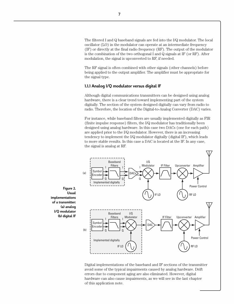
1.1.1 Analog I/Q modulator versus digital IF
Although digital communications transmitters can be designed using analoghardware, there is a clear trend toward implementing part of the system digitally. The section of the system designed digitally can vary from radio toradio. Therefore, the location of the Digital-to-Analog Converter (DAC) varies.
For instance, while baseband filters are usually implemented digitally as FIR(finite impulse response) filters, the I/Q modulator has traditionally beendesigned using analog hardware. In this case two DACs (one for each path)are applied prior to the I/Q modulator. However, there is an increasing tendency to implement the I/Q modulator digitally (digital IF), which leads to more stable results. In this case a DAC is located at the IF. In any case, the signal is analog at RF.
Digital implementations of the baseband and IF sections of the transmitteravoid some of the typical impairments caused by analog hardware. Drifterrors due to component aging are also eliminated. However, digital hardware can also cause impairments, as we will see in the last chapter of this application note.
7
Figure 2.Usual
implementations of a transmitter:
(a) analog I/Q modulator
(b) digital IF
SymbolEncoder
RF LO
UpconverterBaseband
Filters IF FilterI
Q
I/QModulator
IF LO
DAC
I
Q
Implemented digitally
SymbolEncoder
RF LO
UpconverterBaseband
Filters IF FilterI
Q
I/QModulator
IF LO
I
Q
DACs
I
QImplemented digitally
(a)
(b)
Amplifier
Power Control
Amplifier
Power Control

1.1.2 Other implementations
In practice, there are many variations of the general block diagrams discussed above. These variations depend mainly on the characteristicsof the technology used; for example, the type of multiplexing (TDMA orCDMA) and the specific modulation scheme (such as OQPSK or GMSK).1
For instance, GSM1 transmitters can be easily implemented using analog frequency modulators (Figure 3). Since intersymbol interference is not as critical in GSM systems, Gaussian baseband filtering is used instead ofNyquist filters [1]. I/Q modulators are only used in high-performance GSM transmitters.
Different implementations and systems have different design problems andoften require specific measurements. For instance, in TDMA technologies,burst parameters must be measured to ensure that interference with adjacentfrequency channels and adjacent timeslots are within acceptable limits. Themost common measurements and problems associated with particular technologies will be discussed in the following chapters.
The typical receiver (Figure 4) is essentially an inverse implementation of thetransmitter. Although an I/Q demodulator is often used, there are other digitalcommunications receiver designs.
The receiver configuration also depends on the specific system and performance required. For instance, in high-performance cellular receivers,equalization is commonly used to combat ISI caused by impairments in thetransmitter, the air interface or the early stages of the receiver itself.
A more detailed description of digital receivers can be found in the companionHewlett-Packard application note, Testing and Troubleshooting Digital RF
Communications Receiver Designs [5].
8
Figure 3. Block diagram of aGMSK transmitterusing a frequency
modulator
FrequencyModulator
GausianBaseband Filter
1 0 1 1Amplifier
Power Control
1.2 Digital communications
receiver
IF LO
IF Filter
RF LO
BasebandFilters
DemodulatorBit
Decoder
Output (Data or
Voice)
I
Q
Low-NoiseAmplifier with
AutomaticGain Control
PreselectingFilter
Figure 4. Block diagram
of a digital communications
receiver
1. See Glossary for the meanings of these acronyms.

There are several testing stages during the design of a digital communicationstransmitter. The different components and subsections are initially testedindividually. When appropriate, the transmitter is fully assembled, and systemtests are performed. During the design stage of product development, verifi-cation tests are rigorous to make sure that the design is robust. These rigorousconformance tests verify that the design meets system requirements, therebyensuring interoperability with equipment from different manufacturers.
This chapter covers testing of the highlighted part of the transmitter inFigure 1. It describes the conformance tests and other common measurementsmade at the antenna port. Most of the transmitter measurements are commonto all digital communications technologies, although there are some variationsin the way the measurements are performed. Particular technologies, such asCDMA or TDMA, require specific tests that are also described.
Transmitter measurements are typically made at the antenna port, where thefinal signal is emitted. In this case, the measurement equipment is used as anideal receiver.
It may also be necessary to examine the transmitter at various test points as the different sections are designed (see Figure 5). In this case, a stimulussignal might be required to emulate those sections that are not yet available.The equipment for doing this acts as an ideal substitute for the missing circuitor sections. Unmodulated carrier signals have traditionally been used as thestimuli for some component and subsystem measurements, such as frequencyresponse, group delay or distortion measurements. However, complex digitally-modulated stimulus signals are increasingly used, as they may provide more realistic measurement results.
Sometimes individual blocks or components cannot be isolated and the measurement can only be made at the final stage of the transmitter.Therefore, you may be forced to infer the causes of problems from measurements at the antenna port. The ideal testing tool is not only able to perform the measurements but also has the flexibility to provideinsight about system impairments by analysis of the transmitted signal. This application note focuses on transmitter measurements and troubleshootingtechniques performed at the antenna port, although in practice some of these measurements can also be made at other locations in the transmitter.For instance, signal quality measurements can be performed on the RF, IF or baseband sections of the transmitter.
9
Figure 5. Measurement model
2. Testing Transmitter Designs
2.1 Measurement model
SymbolEncoder
RF LO
BasebandFilters IF FilterI
Q
I/QModulator
IF LO
I
Q
Stimulus ("Ideal Source")
Measurements ("Ideal Receiver")
1 0 0 1Amplifier
Power Control

The transmitted signal can be viewed in different domains. The time, frequency and modulation domains provide information on different parameters of a signal. The ideal test instrument can make measurements in all three domains.
Two types of transmitter test instruments are discussed: the spectrum analyzer (SA) and the vector signal analyzer (VSA). Their measurementcapabilities in each domain are described in the following sections of thischapter. Refer to Appendix B for a list of spectrum analyzers and vector signal analyzers from Hewlett-Packard and their capabilities for measuringand troubleshooting digital communications transmitters.
2.2.1 Time domain
Traditionally, looking at an electrical signal meant using an oscilloscope toview the signal in the time domain. However, oscilloscopes do not band limitthe input signal and have limited dynamic range. Vector signal analyzersdownconvert the signal to baseband and sample the I and Q components ofthe signal. They can display the signal in various coordinate systems, such asamplitude versus time, phase versus time, I or Q versus time, and I/Q polar.Swept-tuned spectrum analyzers can display the signal in the time domain as amplitude (envelope of the RF signal) versus time. Their capability can sometimes be extended to measure I and Q.
Time-domain analysis is especially important in TDMA technologies, wherethe shape and timing of the burst must be measured.
2.2.2 Frequency domain
Although the time domain provides some information on the RF signal, it does not give us the full picture. The signal can be further analyzed by looking at its frequency components (Figure 6). Both spectrum analyzers and vector signal analyzers can perform frequency-domain measurements.The main difference between them is that traditional spectrum analyzers areswept-tuned receivers, while vector signal analyzers capture time data andperform Fast Fourier Transforms (FFTs) to obtain the frequency spectrum.In addition, the VSAs measure both the magnitude and phase of a signal.
10
2.2 MeasurementDomains
Time
Amplitude
Frequency
Figure 6.Time and frequency
domains
Measurements in the frequency domain are especially important to ensurethat the signal meets the spectral occupancy, adjacent channel, and spuriousinterference requirements of the system.
2.2.3 Modulation domain
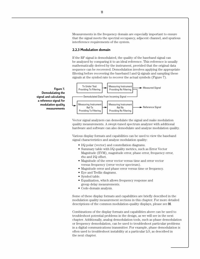
If the RF signal is demodulated, the quality of the baseband signal can be analyzed by comparing it to an ideal reference. This reference is usuallymathematically derived by the instrument, provided that the original datasequence can be recovered. Demodulation involves applying the appropriatefiltering before recovering the baseband I and Q signals and sampling thesesignals at the symbol rate to recover the actual symbols (Figure 7).
Vector signal analyzers can demodulate the signal and make modulation quality measurements. A swept-tuned spectrum analyzer with additionalhardware and software can also demodulate and analyze modulation quality.
Various display formats and capabilities can be used to view the baseband signal characteristics and analyze modulation quality:
• I/Q polar (vector) and constellation diagrams.• Summary table with I/Q quality metrics, such as Error Vector
Magnitude (EVM), magnitude error, phase error, frequency error,rho and I/Q offset.
• Magnitude of the error vector versus time and error vector versus frequency (error vector spectrum).
• Magnitude error and phase error versus time or frequency.• Eye and Trellis diagrams.• Symbol table.• Equalization, which allows frequency response and
group delay measurements.• Code-domain analysis.
Some of these display formats and capabilities are briefly described in themodulation quality measurement sections in this chapter. For more detaileddescriptions of the common modulation-quality displays, please see [1].
Combinations of the display formats and capabilities above can be used totroubleshoot potential problems in the design, as we will see in the next chapter. Additionally, analog demodulation tools, such as phase demodulationor frequency demodulation, can be used to troubleshoot particular problemsin a digital communications transmitter. For example, phase demodulation isoften used to troubleshoot instability at a particular LO, as described in the next chapter.
11
Figure 7.Demodulating the
signal and calculatinga reference signal for
modulation qualitymeasurements
Tx Under TestProviding Tx Filtering
Measuring InstrumentProviding Rx Filtering
Measuring InstrumentRef Tx
Providing Tx Filtering
Measuring InstrumentRef Rx
Providing Rx Filtering
Measured Signal
Reference Signal
Demodulated Data From Incoming Signal

The measurements required to test digital communications transmitters canbe classified as in-band and out-of-band measurements regardless of thetechnology used and the standard followed.
In-band measurements are measurements performed within the frequencyband allocated for the system; for example, 890 MHz to 960 MHz for GSM. In-band measurements can be further divided into in-channel and out-of-channel measurements.
2.3.1 In-channel measurements
The definition of channel in digital communications systems depends on thespecific technology used. Apart from multiplexing in frequency and space(geography), the common cellular digital communications technologies useeither time or code multiplexing. In TDMA technologies, a channel is definedby a specific frequency and timeslot1 number in a repeating frame1, while inCDMA technologies a channel is defined by a specific frequency and code.The terms in-channel and out-of channel refer only to the specific frequencyband of interest (frequency channel), and not to the specific timeslot or codechannel within that frequency band.
2.3.1.1 Channel bandwidth
When testing a transmitter, it is usually a good idea to first look at the spectrum of the transmitted signal. The spectrum shape can reveal majorerrors in the design. For a transmitter with a root-raised cosine filter, the 3dB bandwidth of the modulated frequency channel should approximate the symbol rate. For instance, in Figure 8, for a symbol rate of 1 MHz, the measured 3dB bandwidth is 1.010 MHz. Therefore, this measurement can be used to determine gross errors in symbol rate.
2.3.1.2 Carrier frequency
Frequency errors can result in interference in the adjacent frequency channels. They can also cause problems in the carrier recovery process of the receiver. The designer must ensure that the transmitter is operating on the correct frequency. The carrier frequency should be located in the center of the spectrum for most modulation formats. It can be approximatedby calculating the center of the 3dB bandwidth. For instance, in Figure 8, the measured carrier frequency is 850 MHz.
12
2.3 In-bandmeasurements
1. See Glossary for definition.

Other common methods for determining the carrier frequency are:
• Measure an unmodulated carrier with a frequency counter.• Calculate the centroid of the occupied bandwidth measurement
(see section 2.3.1.4). When performing an occupied bandwidth measurement, the testing instrument usually gives an indication of the frequency carrier error, as shown in Figure 10.
• Use the frequency error metric given in the summary table when performing modulation quality measurements, as shown in Figure 15.
2.3.1.3 Channel power
Channel power is the average power in the frequency bandwidth of the signalof interest. The measurement is generally defined as power integrated overthe frequency band of interest, but the actual measurement method dependson the standard followed [2] [3] [4].
13
Figure 8. Carrier frequency and
channel bandwidthmeasurements
Figure 9. Channel power
measurement
Power is the fundamental parameter of any communication system. The goalin wireless systems is to maintain each link sufficiently with minimum power.This gives two benefits: overall system interference is kept to a minimum and, in the case of mobile stations, battery life is maximized. Output power,therefore, is controlled within tight limits. If a transmitter produces too littlepower, link performance is compromised; too much, and interference withother transmitters may be too high and battery life too short.
In the case of CDMA systems, where total interference is a limiting factor forcapacity, controlling the power of each mobile is also essential to achievemaximum capacity. Therefore, accurate control of the transmitted power iscritical in defining a system’s capacity, coverage and signal quality.
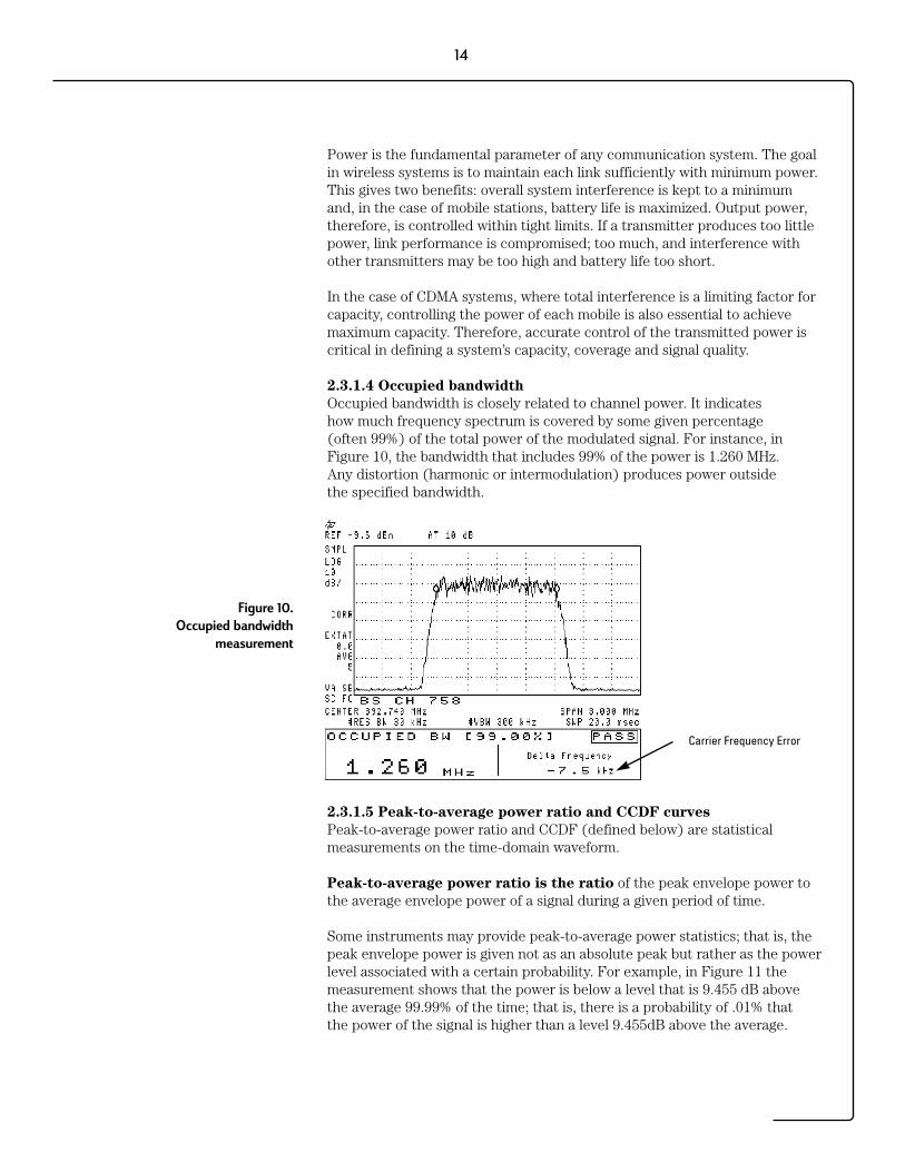
2.3.1.4 Occupied bandwidth
Occupied bandwidth is closely related to channel power. It indicates how much frequency spectrum is covered by some given percentage (often 99%) of the total power of the modulated signal. For instance, inFigure 10, the bandwidth that includes 99% of the power is 1.260 MHz. Any distortion (harmonic or intermodulation) produces power outside the specified bandwidth.
2.3.1.5 Peak-to-average power ratio and CCDF curves
Peak-to-average power ratio and CCDF (defined below) are statistical measurements on the time-domain waveform.
Peak-to-average power ratio is the ratio of the peak envelope power tothe average envelope power of a signal during a given period of time.
Some instruments may provide peak-to-average power statistics; that is, thepeak envelope power is given not as an absolute peak but rather as the powerlevel associated with a certain probability. For example, in Figure 11 the measurement shows that the power is below a level that is 9.455 dB above the average 99.99% of the time; that is, there is a probability of .01% that the power of the signal is higher than a level 9.455dB above the average.
14
Figure 10. Occupied bandwidth
measurement
Carrier Frequency Error

The power statistics of the signal can be completely characterized by performing several of these measurements and displaying the results in agraph known as the Complementary Cumulative Distribution Function
(CCDF). The CCDF curve shows the probability that the power is equal toor above a certain peak-to-average ratio, for different probabilities and peak-to-average ratios. The higher the peak-to-average power ratio, the lower the probability of reaching it.
15
Figure 11. Peak-to-average
power ratio statistics
Figure 12. CCDF curves
Stop: 20 dBStart: 0 dBm% 0.001%
0.01%
0.1%
1%
10%
TRACE B: Ch1 CCDF
100% Cnt: 736k, Avg: –11.088 dBmCnt: 1.34M, Avg: –11.101 dBm
AWGN Signal(used as a reference)
32-Code Channel Signal
9-Code Channel Signal
Prob
abili
ty
dB Above Average

The statistics of the signal determine the headroom required in amplifiers and other components. Signals with different peak-to-average statistics canstress the components in a transmitter in different ways, causing differentlevels of distortion. CCDF measurements can be performed at different pointsin the transmitter to examine the statistics of the signal and the impact of the different sections on those statistics. These measurements can also be performed at the output of the transmitter to compare the statistics to an expected curve. CCDF curves are also related to Adjacent Channel Power(ACP) measurements, as we will see later.
Besides causing higher levels of distortion, high peak-to-average ratios can cause cumulative damage in some components. Performing CCDF measurements at different points of the transmitter can help you prevent this damage.
Peak-to-average power ratio and CCDF statistic measurements are particularly important in digitally-modulated systems because the statisticsmay vary. For instance, in CDMA systems, the statistics of the signal varydepending on how many code channels—and which ones—are present at the same time. Figure 12 shows the CCDF curves for signals with differentcode-channel configurations. The more code channels transmitted, the higher the probability of reaching a given peak-to-average ratio.
In systems that use constant-amplitude modulation schemes, such as GSM,the peak-to-average ratio of the signal is relevant if the components (forexample, the power amplifier) must carry more than one carrier. There is aclear trend toward using multicarrier power amplifiers in base station designsfor most digital communications systems. See [6] for more information onpeak-to-average power ratio and CCDF curves.
2.3.1.6 Timing measurements
Timing measurements are common on TDMA systems, where the signal isbursted. The measurements assess the envelope of the carrier in the timedomain against prescribed limits. Measurements include burst width, risetime, fall time, on-time, off-time, peak power, “on” power, “off” power and duty cycle.
16
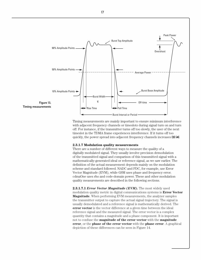
Timing measurements are mainly important to ensure minimum interferencewith adjacent frequency channels or timeslots during signal turn on and turnoff. For instance, if the transmitter turns off too slowly, the user of the nexttimeslot in the TDMA frame experiences interference. If it turns off tooquickly, the power spread into adjacent frequency channels increases [3] [4].
2.3.1.7 Modulation quality measurements
There are a number of different ways to measure the quality of a digitally modulated signal. They usually involve precision demodulation of the transmitted signal and comparison of this transmitted signal with amathematically-generated ideal or reference signal, as we saw earlier. Thedefinition of the actual measurement depends mainly on the modulationscheme and standard followed. NADC and PDC, for example, use ErrorVector Magnitude (EVM), while GSM uses phase and frequency error.cdmaOne uses rho and code-domain power. These and other modulationquality measurements are described in the following sections.
2.3.1.7.1 Error Vector Magnitude (EVM). The most widely used modulation quality metric in digital communications systems is Error Vector
Magnitude. When performing EVM measurements, the analyzer samplesthe transmitter output to capture the actual signal trajectory. The signal isusually demodulated and a reference signal is mathematically derived. Theerror vector is the vector difference at a given time between the ideal reference signal and the measured signal. The error vector is a complex quantity that contains a magnitude and a phase component. It is importantnot to confuse the magnitude of the error vector with the magnitude
error, or the phase of the error vector with the phase error. A graphicaldepiction of these differences can be seen in Figure 14.
17
Burst Width
Rise Time Fall Time
90% Amplitude Points
50% Amplitude Points
10% Amplitude Points
Off-time
Burst Interval or Period
Average Power
Burst Base Amplitude
Burst Top Amplitude
Peak Power
Overshoot
tFigure 13. Timing measurements

Error Vector Magnitude is the root-mean-square (rms) value of the error vector over time at the instants of the symbol clock transitions. By convention, EVM is usually normalized to either the amplitude of the outermost symbol or the square root of the average symbol power [4].
Apart from the constellation and polar diagrams, other important displays associated with EVM that are mentioned in this application note are magnitude of the error vector versus time, the spectrum of the error vector (error vector spectrum), phase error versus time, andmagnitude error versus time. Figure 15 shows some of these displays.
18
Figure 14. Error vector and
related parameters
Figure 15. (a) Polar diagram (b) magnitude of the error vector
versus time (c) error vector
spectrum (d) summary tableand symbol table
Q
I
Magnitude Error
Phase of Error Vector
Measured Signal
Ideal Signal(Reference)
Phase Error
Error Vector
Magnitude of Error Vector
q
f
(a)
(b)
(c)
(d)

EVM and the various related displays are sensitive to any signal flaw that affects the magnitude and phase trajectory of a signal for any digitalmodulation format. Large error vectors both at the symbol points and at thetransitions between symbols can be caused by problems at the baseband, IF or RF sections of the transmitter. As shown in the last chapter of thisapplication note, the different modulation quality displays and tools can helpreveal or troubleshoot various problems in the transmitter. For instance, theI/Q constellation can be used to easily identify I/Q gain imbalance errors.Small symbol rate errors can be easily identified by looking at the magnitudeof the error vector versus time display. The error vector spectrum can helplocate in-channel spurious.
The value of EVM as an indicator of modulation quality can be enhanced by the use of equalization in the measuring instrument. Equalization is commonly used in digital communications receivers. Although its primaryfunction is to reduce the effects of multipath, it also compensates for certainsignal imperfections generated in both the transmitter and receiver. For this reason, it is useful to have an equalizer in the measuring instrument. An instrument with an equalizer will better emulate a receiver; that is, theimpairments that the equalizer of the receiver removes are also removed bythe measuring instrument. Therefore, the impairments that have little effecton system performance also minimally impact the measured EVM. Figure 16shows the magnitude of the error vector versus time with and without equalization. With equalization the constellation looks much better and the magnitude of the error vector versus time is lower. The signal has notchanged, only the measurement technique.
19
Figure 16.Constellation(zoomed) and magnitude of
the error vector versus time (a) without
equalization and(b) with equalization
(a) (b)

2.3.1.7.2 I/Q offset. DC offsets at the I or the Q signals cause I/Q or originoffsets as shown in Figure 17. I/Q offsets result in carrier feedthrough. Some instruments compensate for this error before displaying the constellationor polar diagram and measuring EVM. In that case, I/Q offset is given as a separate error metric.
2.3.1.7.3 Phase and frequency errors. For constant-amplitude modulationformats, such as GMSK used in GSM systems, the I/Q phase and frequencyerrors are more representative measures of the quality of the signal thanEVM. As with EVM, the analyzer samples the transmitter output in order tocapture the actual phase trajectory. This is then demodulated, and the ideal(or reference) phase trajectory is mathematically derived. The phase error is determined by comparing the actual and reference signals. The mean gradient of the phase error signal is the frequency error. The short-term variation of this signal is defined as phase error and is expressed in terms of rms and peak (see Figure 18).
20
Figure 17.(a) Ideal
constellation versus (b) offset
constellation
Q
I
Ideal Constellation
Q
I
Offset Constellation
I/Q Offset
a) b)
Figure 18. Phase and frequency
error measurement

21
Significant phase errors can indicate problems in the baseband section of thetransmitter. The output amplifier in the transmitter can also create distortionthat causes unacceptably high phase error for multicarrier signals. Significantphase error at the beginning of a burst can indicate that a synthesizer is failing to settle quickly enough. In a real system, poor phase error reduces the ability of a receiver to correctly demodulate, especially with marginal signal conditions. This ultimately degrades sensitivity.
Frequency error is the difference between the specified carrier frequencyand the actual carrier frequency. A stable frequency error simply indicatesthat a slightly wrong carrier frequency is being used. Unstable frequencyerrors can indicate short-term instability in the LO, improper filtering, AM-PMconversion in the amplifier, or wrong modulation index if the transmitter isimplemented using an analog frequency modulator. See [3] for more information on phase and frequency error and other GSM measurements.
2.3.1.7.4 Frequency response and group delay. As noted above,equalization compensates for certain signal imperfections in the transmitter,transmission path or receiver. Equalization removes only linear distortion.Linear distortion occurs when the signal passes through one or more lineardevices having transfer functions containing amplitude unflatness (for example, ripple and tilt), and/or group delay variations over the bandwidth of the signal. There can be many sources of linear distortion in a system:bandpass filters in the IF, improper cable terminations, improper baseband filtering, non-compensated sin(x)/x, antenna mismatch, signal combiners and multipath signal effects. From a modeling standpoint, all of the linear distortion mechanisms can be combined and represented by a single transfer function, H(f).
When applying equalization, the measuring instrument must counteract theeffects of the linear distortion. To achieve that, an equalizer filter whosetransfer function is 1/H(f) is applied over the bandwidth of the signal.
Once equalization has been applied, the inverse transfer function of theequalizer, which represents the linear distortion elements of the device undertest, can be displayed and measured. If measured directly at the transmitter’soutput, the inverse transfer function is basically the bits-to-RF frequencyresponse1 of the transmitter (or the variations from the ideal frequencyresponse caused by non-linear distortions) [7]. The actual frequency responsecan be displayed and measured as magnitude, phase, and group delay. Ideally, the magnitude of the frequency response should be flat across the frequency band of interest, and its phase should be linear over that same frequency band. Group delay is a more useful measure of phase distortion. It is defined as the derivative of the phase response versus frequency(dj/dw)—that is, the slope of the phase response. If the transmitter does not introduce distortion, its phase response is linear and group delay is constant. Deviations from constant group delay indicate distortion.
1. See Glossary for definition.

2.3.1.7.5 Rho. CDMA systems use r(rho) as one of the modulation qualitymetrics. Rho is measured on signals with a single code channel. It is the ratio of correlated power to total power transmitted (see Figure 20). The correlated power is computed by removing frequency, phase and time offsets,and performing a cross correlation between the corrected measured signaland the ideal reference. If some of the transmitted energy does not correlate,this excess power appears as added noise that may interfere with other users on the system.
The rho measurement indicates the overall modulation performance level of a CDMA transmitter when transmitting a single channel. Since uncorrelatedpower appears as interference, poor rho performance affects the capacity of the cell [2].
2.3.1.7.6 Code-domain power. In CDMA systems, a signal with multiplecode channels can be analyzed in the code domain. To analyze the compositewaveform, each channel is decoded using a code-correlation algorithm. This algorithm determines the correlation coefficient factor for each code.Once the channels are decoded, the power in each code channel is determined [2].
22
Figure 19. (a) Magnitude of thebits-to-RF frequencyresponse should be
flat across the frequency band of
interest, indicated by (b) 3 dB bandwidth on
signal spectrum
Figure 20.Rho
Power that correlateswith ideal
Total Power
Signal Power
Signal Power +Error Power
Unflatness IndicatesLinear DistortionProblems
Time
P
(a)
(b)
3 dB BW

Measuring code-domain power, as shown in Figure 21, is essential for verifying that the base station is transmitting the correct power in each of the code channels. It is also important to look at the code-domain power levels of the inactive channels, which can indicate specific problems in thetransmitter, as we will see in the last chapter of this application note. Forinstance, unwanted in-channel spurs raise the code-domain noise level.Compression can cause mixing of active code channels to produce energy in particular inactive channels.
2.3.2 Out-of-channel measurements
In-band out-of-channel measurements are those that measure distortion and interference within the system band, but outside of the transmitting frequency channel.
2.3.2.1 Adjacent Channel Power Ratio (ACPR)
Whatever the technology used or standard followed, ACP measurements arerequired to ensure that the transmitter is not interfering with adjacent andalternate channels.
The Adjacent Channel Power Ratio (ACPR) is usually defined as the ratioof the average power in the adjacent frequency channel to the average powerin the transmitted frequency channel. For instance, in Figure 22, the ACPRacross a bandwidth of 1MHz for both the transmitted and adjacent channels is –61.87 dB for the lower adjacent channel and –61.98 dB for the upper adjacent channel. The ACPR is often measured at multiple offsets (adjacent and alternate channels).
23
Figure 21. Code-domain power
measurement

When making ACPR measurements, it is important to take into account thestatistics of the signal transmitted. CCDF curves can be used for this purpose,as we saw earlier. Different peak-to-average ratio values have a differentimpact on the non-linear components of the transmitter, such as the RFamplifier, and therefore on the ACPR as well. Higher peak-to-average ratios in the transmitted signal can cause more interference in the adjacent channel.ACPR measurements on the same transmitter can provide different resultsdepending on the statistics of the transmitted signal. When measuring ACPRin CDMA base stations, for example, it is important to consider the channelconfiguration used.
Different standards have different names and definitions for the ACP measurement. For example, for TDMA systems such as GSM, there are two main contributors to the ACP: the burst-on and -off transitions, and the modulation itself. The GSM standards name the ACP measurement Output RF Spectrum (ORFS) and specify two different measurements:ORFS due to modulation and ORFS due to switching [3].
In the case of NADC-TDMA, the ACP due to the transients and the modula-tion itself are also measured separately for mobile stations. Additionally, aweighting function that corresponds to the receiver baseband filter responseis applied to the measurement for both base and mobile stations [4].
Spectral splatter is a term often associated with the ACP due to transients.Spectral splatter can be caused by fast burst turn-on and turn-off, clipping(saturation) and Digital Signal Processor (DSP) glitches or other errors due to scaling. High spectral splatter may occasionally be caused by phasetransients. Since transients are very short events, time capture can be useful to locate and analyze them. Spectral splatter can also be analyzedusing a spectrogram, which displays spectrum versus time, as shown in Figure 74 (section 3.2.11).
24
Figure 22. ACPR measurement

For cdmaOne systems, the ACPR is not defined in the standard, but it is oftenused in practice to test the specified in-band spurious emissions [2].
Spectral regrowth is a measure of how much the power in the adjacent channel grows (how much worse it gets) for a specific increment of the transmitted channel power.
2.3.2.2 Spurious
Spurious signals can be caused by different combinations of signals in thetransmitter. The spurious emissions from the transmitter that fall within the system’s band should be below the level specified by the standard to guarantee minimum interference with other frequency channels in the system (see Figure 23) [2] [3].
Out-of-band measurements are those outside the system frequency band.
2.4.1 Spurious and harmonics
While spurious are caused by different combinations of signals in the transmitter, harmonics are distortion products caused by nonlinear behaviorin the transmitter. They are integer multiples of the transmitted signal’s carrier frequency.
Out-of-band spurious and harmonics are measured to ensure minimum interference with other communications systems (Figure 24) [2] [3].
25
Figure 23.In-band spurious
measurement
2.4 Out-of-bandmeasurements

By following certain guidelines in conducting design verification tests, youcan greatly increase the probability that the transmitter will operate properlyin the real-world environment. The test equipment should be carefully chosento reduce measurement uncertainties and increase confidence in correcttransmitter operation.
When performing absolute power measurements, such as channel power, the accuracy of the measurement is limited by the absolute amplitude accuracy of the instrument. In the case of relative power measurements, such as ACPR, the accuracy is limited by the relative amplitude accuracy and dynamic range of the instrument. As a rule of thumb, the noise floor ordistortion of the instrument should be at least 10 dB below the distortion of the signal being measured.
Since the signal is noise-like, averaging the power over several measurementsis extremely important for more repeatable power measurements [8].
In the case of timing measurements, the accuracy of the measurement ismainly limited by the time accuracy, time resolution, and amplitude linearityof the instrument. Since there are a number of parameters to measure, theuse of masks and pass/fail messages makes it simpler to ensure that all thetiming parameters meet their specifications.
The accuracy of modulation quality measurements is mainly limited by theaccuracy of the test instrument, which is usually given as a percentage.Typically, the test equipment should be ten times more accurate than the specified limit so measurement results can be attributed to the unit-under-test (UUT) and not to the measuring instrument.
26
Figure 24. Out-of-band spurious
and harmonics measurement
2.5 Best practices in conducting
transmitter performance
tests

Transmitter designs are tested to ensure conformance with a particular standard and are typically performed at the antenna port. However, substandard performance may be caused by various parts of the system, so troubleshooting is usually done at several points in the transmitter. The source of impairments can be difficult to determine. This difficulty is magnified by these practicalities:
• Part of the transmitter is generally implemented digitally.• Some parts of the transmitter may not be accessible.• It may be unclear whether a problem is rooted in the analog or
digital section of the system.
The ability to look at the signal and deduce the source of a problem is veryimportant to successful design. The ideal troubleshooting instrument has theflexibility and measurement capabilities to help you infer problem causesfrom measurements at the RF, IF and baseband sections of the transmitter.
The measurements described in this chapter are performed at the antennaport, assuming that other parts of the transmitter are not easily accessed. The objective is to help you recognize and troubleshoot the most commonimpairments from measurements performed at the antenna port. To assistyou in this task, the following information is included in this chapter:
• A general troubleshooting procedure (see Appendix A for a more detailed procedure).
• A table that links measurement problems to their possible causes in the different sections of the transmitter.
• A description of the most common impairments, and an explanation of how to verify each one of them.
The following is a suggested troubleshooting procedure to follow if the transmitter design does not meet the specifications:
1.Look at the signal in the frequency domain and verify that its spectrum appears as expected. Ensure that its center frequency and bandwidth are correct.
2.Perform in-band and out-of-band power measurements: channel power, ACP (check CCDF curve), spurious and harmonics.
3. In the case of bursted signals, perform timing measurements.4.Look at the constellation of the baseband signal.5.Examine error metrics (EVM, I/Q offsets, phase error, frequency error,
magnitude error and rho).6. If the phase error is significantly larger than the magnitude error,
examine I/Q phase error versus time. Perform phase noise measurements on LOs, if accessible.
7. If phase error and magnitude error are comparable, examine magnitude of the error vector versus time and error vector spectrum.
8.Turn the equalizer on and verify that it reduces modulation quality errors, and check frequency response and group delay of the transmitter for faulty baseband or IF filtering or other linear distortion problems.
27
3. TroubleshootingTransmitterDesigns
3.1 Troubleshooting procedure

In these measurements, variations from the expected results will help youlocate faults in different parts of the transmitter. The following sectionsdescribe the most common impairments and how to recognize them fromtheir effects on the different measurements.
Refer to Appendix A for a more detailed troubleshooting procedure.
Table 1 will help you identify the most common impairments that might beaffecting a specific measurement when you are testing your design.
For instance, a high level of ACP is probably caused by one of the followingimpairments:
• Compression at the amplifier• Wrong filter coefficient or incorrect windowing at the baseband filter. • Incorrect interpolation.• LO instability.• Burst-shaping error.• DAC/DSP error.• A severe case of symbol rate error.
You can further analyze and verify if any of these impairments is present byfollowing the directions given in the following sections.
28
Table 1. Impairments versus
measurements affected
3.2 Impairments
Channel BW
Channel Power
CCDF
ACP
Spurious
Timing
EVM(or Phase Error)
Code-DomainPower (or rho)
Bits-to-RFFrequencyResponse(& Group Delay)
Com
pres
sion
I/Q
Err
or
Sym
bol R
ate
Wro
ng F
ilter
Coe
ffici
ents
or W
indo
win
g
Wro
ng In
terp
olat
ion
IF F
ilter
Tilt
or R
ippl
e
LO
Inst
abili
ty
In
terfe
ring
Tone
AM
-PM
Con
vers
ion
D
AC/D
SP E
rror
Bur
st-S
hapi
ng E
rror
ImpairmentsM
easu
rem
ents
Affe
cted
High probability that impairment affects the measurementSevere cases of impairment may affect the measurement

3.2.1 Compression
The power amplifier (PA) is the final stage prior to transmission. Key characteristics of the PA are frequency and amplitude response, –1dB compression point and distortion. The PA selected must be appropriate for the signal type. To avoid compression of the signal, the input levels andoutput section gains in the amplifier must be tightly controlled.
Compression occurs when the instantaneous power levels are too high, driving the amplifier into saturation. For instance, if the signal peak power isnot properly taken into account, signal compression can occur. This issue isparticularly relevant to CDMA systems, because the peak-to-average ratio of the multi-code signal changes depending on the channel configuration.Mobile station transmitters that use constant-amplitude modulation schemes(like GSM mobile station transmitters), which only carry information on thephase of the signal, are more efficient when slightly saturated. But in otherdigitally-modulated systems, compression causes clipping and distortion,which may result in a loss of signal transmission efficiency and cause interference with other channels.
How can you verify compression?
The best way to verify that the signal is compressed is to make ACPR andCCDF measurements before and after the amplifier and compare the results.If measurements in front of the amplifier are not possible, you can lower theamplitude of the transmitted signal and compare measurement results. In the case of ACPR, if the peak amplitude of the transmitted signal drives theamplifier into compression, distortion occurs, and the distortion in adjacentfrequency channels is larger than expected. Therefore, the measured ACPR is smaller.
29
Figure 25. Power amplifier
SymbolEncoder
RF LO
BasebandFilters IF FilterI
Q
I/QModulator
IF LO
I
Q
Other ChannelOther Channel
Other ChannelOther Channel
1 0 0 1Amplifier
Power Control

In the case of peak-to-average ratio and CCDF statistics, if compressionoccurs, the peak levels of the transmitted signal are clipped. Clipping causes a peak-to-average ratio reduction. Therefore, the CCDF curve shows lowerprobabilities of reaching large peak-to-average ratios—that is, the peak-to-average ratio is smaller for a certain probability, as shown in Figure 27.
30
Figure 26. ACP increases whencompression occurs
Stop: 20 dBStart: 0 dBM% 0.001%
0.01%
0.1%
1%
10%
TRACE C: D3 CCDF
100% Cnt: 130k, Avg: –21.062 dBmCnt: 206k, Avg: 4.45 dBm
AWGN Signal(used as a reference)
Prob
abili
ty
dB above Average
Compressed QPSKSignal
Non-compressed QPSKSignal
Figure 27. CCDF curves
for signal with and without
compression
With Compression
Without Compression

Compression may also be detected in other measurements:
• Polar diagram. If the high peak levels of the transmitted signal are clipped, the signal has a lower overshoot. This effect can be seen by comparing the trajectory of the compressed signal to the ideal trajectoryin the polar diagram, as in Figure 28. Filtering at the receiver causes dispersion in time. In practice, compression often causes an error in the symbol(s) after a peak excursion of the signal. Therefore, EVM may be affected.
• Code-domain power. Non-linearity in the amplifier also causes an increase in the code-domain noise level in CDMA systems. Compression causes code-domain mixing. Therefore, energy appears in the non-active channels in deterministic ways. For instance, in Figure 29, for a cdmaOne signal, Walsh code1 1 mixes with Walsh codes 12 and 32, causing energy to show up on Walsh codes 13 and 33. Also, Walsh code 12 mixes with Walsh code 32 to create power on Walsh code 44.
Compression is not a linear error and cannot be removed by equalization.
31
Figure 28.Polar diagram of
compressed signal(compared to ideal
trajectory)
Figure 29. Code-domain
power for (a) non-compressed
signal versus (b) compressed signal
1. See Glossary for definition.
ActualTrajectory
Reference (Ideal Trajectory)
Mixing Products
(a) (b)

I/Q Impairments
I/Q impairments can be caused by matching problems due to component differences between the I side and Q side of a network. The most common I/Qimpairments are listed below:
1. I/Q gain imbalance. Since I and Q are two separate signals, each one is created and amplified independently. Inequality of this gain between the I and Q paths results in incorrect positioning of each symbol in the constellation, causing errors in recovering the data (see Figure 31). Thisproblem is rare in systems where the IF is implemented digitally.
2. Quadrature errors. If the phase shift between the IF (or RF) LO signals that mix with the I and Q baseband signal at the modulator is not 90 degrees, a quadrature error occurs. The constellation of the signal is distorted (see Figure 32), which may cause error in the interpretation of the recovered symbols.
32
SymbolEncoder
RF LO
IF Filter
I
Q
BasebandFilter
BasebandFilter
IF LO
0 deg
90 deg
GQ
GI
SAmplifier
Power Control
1 0 0 1
Figure 30.I/Q modulator
Figure 31. I/Q gain imbalance

3. I/Q offsets. DC offsets may be introduced in the I and Q paths. They maybe added in the amplifiers in the I and Q paths. For digital IF implementations,offsets may also occur from rounding errors in the DSP. See Figure 33.
4. Delays in the I or Q paths. When the serial bit stream is encoded intosymbols and the bits are split into parallel paths for creation of the I and Qsignals, it is important that these signals are properly aligned. Problems inthis process can cause unwanted delays between the I and Q signals. Delayscan be caused by the modulator or by the previous components in the I or Qpaths (for example, the baseband filter or the DAC). For instance, if the baseband filters are analog, variations in group delay between the filterscause different delays in the I and Q paths. Different electrical lengths in the I and Q paths may also cause significant delay differences between thetwo paths, especially for signals with wide bandwidths (high symbol rates).Refer to Figure 34.
33
Figure 32. Quadrature error
Figure 33. I/Q offsets

5. I/Q swapped. Swapping the I and Q signals reverses the phase trajectoryand inverts the spectrum around the carrier. Therefore, swapping the I and Qor changing the sign of the shift (+90 or –90 degrees) makes a difference inthe signal transmitted: cos(wLOt)–jsin(wLOt) versus cos(wLOt)+jsin(wLOt).The mapping of the IF I and Q signals is reversed, which causes symbolerrors, as seen in Figure 35.
34
2
3 1,4
Q
I
1 2 3 4
Q
-1
+1
I
-1
+1
I/Symbol Rate
2
31,4
Q
I
1 2 3 4
-1
+1
-1
+1
I/Symbol Rate
Delay
Figure 34. Q delayed relative to I
10 00
11 01
I and Q Swapped
Q
I
10 00
11 01
Q
IFigure 35.I/Q swapped

How can you verify the different I/Q impairments?
The best way to verify most I/Q impairments is to look at the constellation
and EVM metrics.
I/Q gain imbalance results in an asymmetric constellation, as seen in Figure 31. Quadrature errors result in a “tipped” or skewed constellation,as seen in Figure 32. For both errors the constellation may tumble randomlyon the screen. This effect is caused by the fact that the measuring instrumentdecides the phases for I and Q periodically, based on the data measured, andarbitrarily assigns the phases to I or Q. Using an appropriate sync word as atrigger reference makes the constellation stable on the screen, permitting thecorrect orientation of the symbol states to be determined. Therefore, the relative gains of I and Q can be found for gain imbalance impairments, andthe phase shift sign between I and Q can be determined for quadrature errors.
I/Q offset errors may be compensated by the measuring instrument whencalculating the reference. In this case, they appear as an I/Q offset metric.Otherwise, I/Q offset errors result in a constellation whose center is offsetfrom the reference center, as seen in Figure 33. The constellation may tumblerandomly on the screen unless a sync word is used as a trigger, for the samereason indicated above.
Delays in the I or Q paths also distort the measured constellation.However, if the delay is an integer number of samples, the final encoded symbols transmitted appear positioned correctly but are incorrect. The errorcannot be detected unless a known sequence is measured. Mathematicalfunctions in the measuring instrument can help compensate for delaysbetween I and Q, by allowing you to introduce delays in the I or Q paths. In this way, you can confirm and measure the delay.
For any of these errors, magnifying the scale of the constellation can helpdetect subtle imbalances visually. Since the constellation is affected, theseerrors deteriorate EVM.
I/Q swapped results in an inverted spectrum. However, because of the noise-like shape of digitally-modulated signals, the inversion is usually undetectable in the frequency domain. In the modulation domain, the datamapping is inverted, as seen in Figure 35, but the error cannot be detected,unless a known sequence is measured. In CDMA signals, I/Q swapping errorscan be detected by looking at the code-domain power display. Since theseerrors result in an incorrect transmitted symbol sequence, the measuringinstrument can no longer find correlation to the codes. This causes an unlockcondition, in which the correlated power is randomly distributed among allcode-channels, as shown in Figure 36. Some vector signal analyzers have aninverted frequency mode that accounts for this error and allows you verify it.
35

Code-domain power is affected by any I/Q impairment. Basically, any impairment that degrades EVM will cause an increase in the code-domain-power noise floor—that is, an increase in the level of non-active channels.Figure 37 shows an increase in the code-domain-power noise floor for acdmaOne system with an I/Q gain imbalance of 3 dB.
I/Q impairments are not linear errors and therefore cannot be removed byapplying equalization.
36
Figure 36. (a) Normal versus
(b) unlock conditionfor code-domain
power (power randomly distributed
among all code-channels)
Figure 37. Increase in
code-domain-powernoise floor
(right versus left)
(a) (b)

3.2.3 Incorrect symbol rate
The symbol clock of a digital receiver system dictates the sampling rate of thebaseband I and Q waveforms. To accurately interpret the symbols and recoverthe digital data at the receiver, it is imperative that the transmitter and thereceiver have the same symbol rate.
The symbol clock in the transmitter must be set correctly. Symbol rate errors often occur from using the wrong crystal frequency (for example, iftwo numbers are swapped in the frequency specification). Slight errors in theclock frequency impair the signal slightly, but as the frequency error increasesthe signal can become unusable. Therefore, it is important to be able to verifyerrors in the symbol timing.
How can you verify errors in the symbol rate?
The effect of symbol rate errors on the different measurements depends onthe magnitude of the error. If the error is large enough, the instrument cannotdemodulate the signal correctly and modulation quality measurements aremeaningless. For instance, for a QPSK system with a specified symbol rate of 1 MHz, an error of 10 kHz (actual symbol rate of 1.010 MHz) can cause anunlock condition when looking at the constellation and measuring EVM. For aW-CDMA system with a specified symbol rate of 4.096MHz, an error of 200Hz(actual symbol rate of 4.0962) causes an unlock condition in the code-domainpower measurement.
Therefore, the methods to verify small symbol errors (those that do not causean unlock condition) and large symbol errors (those that create an unlockcondition) are different.
Small errors
The best way to verify small errors in the symbol rate is by looking at themagnitude of the error vector versus time display. If the symbol rate is slightly off, this display shows a characteristic ‘V’ shape, as in Figure 39b.
37
SymbolEncoder
RF LO
BasebandFilters IF FilterI
Q
I/QModulator
IF LO
I
Q
Amplifier
Power Control
1 0 0 1
Figure 38. Symbol encoder

This effect can be understood by studying Figure 40. For simplicity, asinewave is used instead of a digitally-modulated signal, and its frequency(symbol rate) is slightly higher than the specified sample frequency (symbolrate chosen in the measuring instrument). At one arbitrary reference sample(called 0) the signal will be sampled correctly. Since the symbol rate is slightlyoff, any other sample in the positive or negative direction will be slightly off in time. Therefore, the signal will deviate by some amount from the perfect reference signal. This deviation or error vector grows linearly (on average) in both the positive and negative directions. Therefore, the magnitude of the error vector versus time shows a characteristic ‘V’ shape.
The smaller the symbol rate error, the more symbols are required todetect the error (that is, to form the ‘V’ shape). For instance, in Figure 39b,for a QPSK system with a symbol rate specified at 1MHz, 100 symbols aremeasured to form a “V” shape in the magnitude of the error vector versustime display for an actual symbol rate of 1.0025 MHz. In the same case, about 500 symbols are required to form a similar ‘V’ shape for an actual symbol rate of 1.00025 MHz.
38
Figure 39. (a) Constellation and(b) magnitude of the
error vector versustime with ‘V’ shape
caused by incorrectsymbol rate
Actual Symbol Period
Sample Period
-2 -1 0 1 2
Error 1 or -1
Error 2 or -2
-2 -1 0 1 2
210
Graph of Error at Each Sample
Figure 40. Symbol rate slightlyhigher than specified
(a)
(b)

The actual transmitted symbol rate can be found by adjusting the symbol ratein the measuring instrument by trial and error until magnitude of the errorvector versus time looks flat.
Small symbol errors also affect the code-domain power measurement. The code-domain power noise floor increases proportionally to the magnitudeof the error.
Large errors
The best way to verify large symbol rate errors that produce unlock conditionsin the measurements is by measuring the signal’s channel bandwidth toroughly approximate the symbol rate, as explained in section 2.3.1.1.
Errors in the symbol rate are not linear and cannot be minimized by applying equalization.
3.2.4 Wrong filter coefficients and incorrect windowing
Baseband filtering must be correctly implemented to provide the right baseband frequency response and avoid intersymbol interference and overshoot of the baseband signal. In systems using Nyquist filters, the roll-off parameter, alpha, defines the sharpness of the filter in the frequencydomain. As shown in Figure 42, the lower the alpha, the sharper the filter in the frequency domain and the higher the overshoot in the time domain. It is important to verify that the transmitter has the appropriate basebandfrequency response for the alpha specified.
39
SymbolEncoder
RF LO
IF Filter
I
Q
BasebandFilter
BasebandFilter
IF LO
0 deg
90 deg
GQ
GI
1 0 0 1
SAmplifier
Power Control
Figure 41. Baseband filters
-4 0 0.20 0.4 0.6 0.8fj/Fsymbol
Hj
ti/T
0
1
hi
a=.5
a=0a=1
a=0.5(a) (b)
-2 2 4
a=1 a=0
10
1
Figure 42. (a) Time and
(b) frequencyresponse of
raised cosine filters with
different alphas

In many communications systems using Nyquist baseband filtering, the filterresponse is shared between the transmitter and the receiver. The filters mustbe compatible and correctly implemented in each. The type of filter and theroll-off factor (alpha) are the key parameters that must be considered.
The main causes of error in baseband filtering are the following:
1. Wrong filter coefficients. For Nyquist filters, an error in the implemen-tation of alpha may result in undesirable amplitude overshoot in the signal or interference in the adjacent frequency channel. It may also degrade intersymbol interference (ISI) caused by fading.
2. Incorrect windowing of the transmitter filter. Since the ideal frequency response of the Nyquist filter is finite, the ideal time response(impulse response) is infinite. However, the baseband filter is usually implemented as a digital FIR filter, which has a finite impulse response; that is, the actual time response is a truncated version of the ideal (infinite)response. The filter must be designed so that it does not truncate the idealresponse too abruptly. Also, the filter must include enough of the idealimpulse response to prevent excessive distortion of the frequency response.
For example, Figure 43a shows the ideal time response and frequencyresponse of a root-raised cosine filter for an alpha of 0.2. Figure 43b showsthe actual time response after a flat time window has been applied. Sincesamples of significant value have been truncated, the actual time response issignificantly different from the ideal, and the frequency response is distorted.The time window applied by the actual filter must be appropriate for thespecified alpha to avoid too much distortion of the frequency response. Inthis case (Figure 43), the window applied is too short (in time), whichincreases ACP in the frequency domain.
40
-10 -5 0 5 10 0 0.2 0.4 0.6 0.8 1
0.5
0.2
0
0.4
fj/Fsymbol
Hj
Time Domain Frequency Domain
-10 -5 0 5 10 0 0.2 0.4 0.6 0.8 1
0.5
0.2
0
0.4
fj/Fsymbol
Hj
ti
T
hi
0
1
hi
0
1
Figure 43. Incorrect windowing
distorts the frequencyresponse
(a)
(b)

How can you verify errors in the alpha coefficient and the windowing?
The main indicator of a wrong alpha coefficient and incorrect windowing is the display of magnitude of the error vector versus time. In systemsthat use Nyquist filtering, an incorrect alpha (or a mismatch in alpha betweentransmitter and receiver) causes incorrect transitions while the symbol pointsthemselves remain mostly at the correct locations. Therefore, the EVM is largebetween the symbols, while it remains small at the symbol points. Figure 44shows that effect for a mismatch between the transmitter filter (alpha = 0.25)and the receiver filter in the measuring instrument (alpha = 0.35, as specifiedfor a particular system). Incorrect windowing has the same effect, since theactual baseband response of the transmitter and the baseband responseapplied in the measuring instrument no longer match. The amplitude overshoot of the baseband signal depending on the alpha can be observed in the polar diagram.
Baseband filtering errors may also appear in the following measurements:
• Channel bandwidth. The 3dB bandwidth of a root-raised cosine filter is independent of the filter coefficient alpha. However, incorrect windowing may cause a dramatic change of the spectrum that may affect the 3dB bandwidth.
• CCDF curves. The roll-off factor, alpha, affects the amount of overshoot. Therefore, a filter with the wrong parameter may affect the statistics of the signal.
• ACP. Incorrect filtering may affect the degree of interference in theadjacent channel. The windowing applied in time also affects the ACP. The shorter the time window, for a particular alpha, the worse the ACPR. More abrupt time windows also cause a larger ACPR.
• Code-domain power. Distortion caused by mismatched filters can result in an increase in the code-domain noise floor.
• Frequency response. The frequency response of the baseband filter affects the total frequency response of the transmitter. Therefore, the effect of wrong filter coefficients or incorrect windowing can be analyzed by applying equalization and examining the transmitter’s bits-to-RF frequency response, as seen in Figure 45a.
41
Figure 44. (a) Polar
diagram and (b) magnitude of the
error vector versustime for incorrect
alpha. The error vector is large
between symbolpoints and small at
the symbol points
(a)
(b)
Small Error Vector at Symbol Points

Equalization minimizes the errors caused by baseband filtering impairments.Figure 45b shows how equalization improves magnitude of the error vectorversus time (compare to Figure 44b).
3.2.5 Incorrect interpolation
As we saw earlier, baseband filters in the transmitters are usually implementedas digital filters. Digital techniques ensure that we can reproduce filters asmany times as desired with exactly the same characteristics.
Since the RF signal is analog, the digital signal has to be converted to analogat some point in the transmitter. After the DAC used for that purpose, ananalog reconstruction filter smooths the recovered analog signal by filteringout the unwanted frequency components. As per the Nyquist criteria, thesampling frequency should be at least twice the highest frequency componentof the signal being sampled. In the case of a digitally-modulated signal, sampling at the symbol rate does not meet the Nyquist criterion. When recovering the analog signal, filtering could be an issue, and significant aliasing can occur, as shown in Figure 47.
42
Figure 45. (a) Frequencyresponse for
incorrect alpha.(b) Magnitude of the
error vector versustime improves with
equalization
SymbolEncoder
RF LO
IF Filter
I
Q
BasebandFilter
BasebandFilter
IF LO
0 deg
90 deg
GQ
GI
SAmplifier
Power Control
1 0 0 1
Figure 46. Baseband filters
(a)
(b)

Therefore, it is recommended to use a sample rate at least twice as high as the symbol rate. This is accomplished by interpolating. The technique generally used consists of adding zeros between the samples before applyingbaseband filtering, as shown in Figure 48. Since the samples added are zeros,the time response of the filter is not affected. The only effect is to provideextra data points between the symbols. This better describes the transitionsbetween waveforms. In the frequency domain, the images are now shiftedmuch higher in frequency, thereby reducing the requirements of thereconstruction filter to a reasonable level.
43
...
Incorrect AmplitudeValues at SymbolClock Transitions
BasebandFilter
DAC
ReconstructionFilter
a)
b)
fsample
...
fsample 2fsample fsample 2fsampleAliasing
Figure 47. Sample rate = symbol rate.
Effect in (a) the time domain
and (b) frequency domain
...
Correct AmplitudeValues at SymbolClock Transitions
BasebandFilter
DAC
ReconstructionFilter
a)
b)
fsample
...
fsample
...
InterpolatedSamples
...
Figure 48. Interpolation: sample rate =
4 x symbol rate. Effect in the
(a) time domain and(b) frequency domain

It is a common mistake to interpolate the I and Q signals as if they were pulses, instead of impulses. In other words, instead of adding zeros, it is acommon mistake to add samples that have the same value as the original samples. The response of the filter is then affected, as shown in Figure 49.The frequency response of an impulse is a constant amplitude. When multiplied by the frequency response of the baseband filter, the correct spectrum is obtained. The frequency response of a pulse in the time domainis a sin(x)/x function, where x=pft and t is the width of the pulse. When thepulse signal is filtered, its frequency response gets multiplied with the filter’sresponse. The result, for a transmitter with analog I/Q modulation, is anincorrect spectrum that has a rounded top instead of a flat one. In the case of a transmitter with digital IF, this error could cause different effects.
If different sections of the transmitter are designed with different samplingrates, an interpolation problem may also occur. For instance, if the FIR filter(or the digital IF section) and the DAC work at different rates, some kind ofinterpolation between these sections is required. In this case, either addingzeros or samples equal to the original ones to the signal between the two sections may distort the signal.
How can you verify interpolation errors?
Since incorrect interpolation modifies the overall baseband filter frequency response, intersymbol interference occurs. Therefore, the polar
or constellation diagram and EVM are degraded. The best way to verifyinterpolation errors is by applying equalization to remove the effects of thoseerrors in the polar or constellation diagram and EVM (see Figure 50), andchecking the bits-to-RF frequency response. Assuming there are no otherlinear errors, the frequency response should look similar to the sin(x)/x function that the equalizer is compensating for, as shown in Figure 51.
Incorrect interpolation can also affect the following measurements:
44
BasebandFilter
a)
b)
...
Himpulse(f) Hf(f)
Hf(f)Hpulse(f)=sin(x)/x
BasebandFilter
... ...
...
Figure 49. Effects of
(a) correct 4x interpolation versus
(b) incorrect interpolation

• Channel bandwidth. Incorrect interpolation has an impact on the spectrum shape. For instance, for a transmitter with analog I/Q, the spectrum of a signal with incorrect interpolation has a rounded top instead of a flat one. Therefore, the channel bandwidth measurement may be affected. For example, Figure 52 shows a 3 dB bandwidth of 665 kHz for a signal with a symbol rate of 1 MHz.
45
Figure 50. Effect of equalization
on signal with incorrect interpolation:
polar diagram and magnitude of the error
vector versus time (a) without
equalization and (b) with equalization
Figure 51. Bits-to-RF frequency
response of transmitterwith incorrect interpolation
(a) (b)

• CCDF curves. Incorrect interpolation may distort the signal and, therefore, its statistics may change.
• ACP. Incorrect interpolation may cause an increase in the ACP.• Code-domain power. Since EVM is degraded, the code-domain
power noise floor may increase.
3.2.6 IF filter tilt or ripple
The IF filter eliminates out-of-channel interference created during the I/Q modulation. Error characteristics in the design of this filter can affect the resulting signal. Ideally, the filter should be flat across the frequency band of interest and its group delay should be constant across the same frequency band. Common IF filter impairments include filter tilt or ripple inthe frequency response and variations of group delay. For instance, SAW(Surface Acoustic Wave) filters may have internal reflections that cause longdelays, which produce fine-grain ripple in the frequency response. Filter tiltor ripple in the frequency response causes linear distortion in the signal.
46
Figure 52. Spectrum of signal
with incorrect interpolation
SymbolEncoder
RF LO
BasebandFilters IF FilterI
Q
I/QModulator
IF LO
I
Q
Amplifier
Power Control
1 0 0 1
Figure 53. IF filter

An effect equivalent to filter tilt or ripple is often caused by improper matching of any component from the IF filter to the antenna. For example,mismatch between the RF amplifier and the antenna or between any components in the IF or RF section of the transmitter may cause reflections that result in distortion of the overall transmitter’s frequency response. The distortion is either tilt or ripple, depending on the distance between the mismatched components and the bandwidth of the signal. As you can seein Figure 54, for narrow bandwidths relative to the inverse of the distancebetween the components, the frequency shape appears tilted. For wide bandwidths it appears rippled. The effect of mismatch between componentsis usually negligible for the bandwidths used in wireless RF applications (BW << 1/di), while it becomes more important in applications using widerbandwidths, such as LMDS (Local Multipoint Distribution System) or satellite applications.
How can you verify filter tilt or ripple?
Filter tilt or ripple causes distortion of the demodulated baseband signal.Therefore, the constellation and EVM are degraded. The best way to verifyIF filter errors or equivalent effects is by applying equalization to the signaland checking the bits-to-RF frequency response. Equalization removeslinear distortion. Therefore, both the constellation and magnitude of the errorvector versus time should improve noticeably. Assuming that there are noother linear errors in the transmitter, the bits-to-RF frequency responseshows the ripple or the tilt, as seen in Figure 55.
47
Amplifier
RF LO
UpconverterIF Filter
d2 d3
d4
if BW<1/di
if BW>>1/di
d1
f
Figure 54. Mismatch between IF
or RF componentsmay cause tilt or
ripple in the frequency response

In the case of SAW filters, the time delays in the filter impulse response canbe further analyzed by increasing the equalizer filter length and observing theequalizer impulse response.
Filter tilt or ripple may also appear in the following measurements:
• Channel bandwidth. Tilt and ripple may show subtly in the frequency domain if averaging is applied.
• CCDF curves. Tilt or ripple affect the statistics of the signal, and therefore the CCDF curves.
• Code-domain power. Filter tilt or ripple can also raise the code-domain power noise floor.
3.2.7 LO instability
The RF LO characteristics are passed on to the final RF signal. If the frequency is unstable, the channel occupation restrictions may be violatedand interference with adjacent channels may occur. LO instability may becaused by hum or other signals that run close to the LO. For instance, datalines (typically CMOS1) carry signals with steep edges that can couple RFenergy to an LO. Phase noise in any LO in the transmitter can also causenoise in the phase of the recovered I/Q signal. Phase noise at far offsets in the RF LO may be fed through and cause energy to be spilled into the adjacent channel.
48
Figure 55. Bits-to-RF frequency
response of a transmitter with
IF filter tilt
SymbolEncoder
RF LO
BasebandFilters IF FilterI
Q
I/QModulator
IF LO
I
Q
Upconverter Amplifier
Power Control
1 0 0 1
Figure 56. IF and RF LOs
1. See Glossary.

How can you verify LO instability?
A large phase error relative to the magnitude error gives the best indicationof instability in an LO. The error can be further analyzed by examining thephase error versus time display. This display shows the modulating waveform of any residual or interfering PM signal. Random phase errors indicate phase noise, while sinewave shapes or periodic waveforms indicateinterfering PM tones. For example, Figure 57 shows the phase error versustime for a signal with a symbol rate of 50 kHz. Since the phase error versustime shows two cycles over 2000 symbols, the frequency of the interfering PM signal is 2x(50x103)/2000 = 50 Hz.
If the LOs in the transmitter are accessible, the problem can be tracked downto a specific LO by making analog PM measurements on the different LOs ofthe transmitter.
Bad cases of LO interference cause a constellation display like that shownin Figure 58. The measured symbols preserve the right amplitude but vary inphase around the ideal symbol reference point.
49
Figure 57. Phase error versus
time for a signal with hum
Figure 58. Constellation display
degraded by phasenoise

LO instability also impacts the following measurements:
• Adjacent Channel Power. As indicated earlier, residual PM or phase noise at far offsets in the RF LO can degrade the ACP (see Figure 59).
• Code-domain power. LO instability appears in the code-domain power display as an increase in the noise level in certain non-active code channels. The code channels affected depend on the orthogonal coding scheme of the particular system and on the code-channel configuration of the signal. Figure 60 shows the code-domain power display for a signal with phase noise.
LO instability is not a linear error and cannot be removed by equalization.
50
Figure 59.ACP degraded by
phase noise at far offsets
Figure 60. Code-domain power
for signal (a) without phase
noise and (b) with phase noise
High Phase Noise at Far Offsets
Low Phase Noise
(a) (b)

3.2.8 Interfering tone
A tone or spur generated anywhere in the transmitter can interfere with thetransmitted signal if it falls in the signal’s bandwidth. In-channel interferingtones are usually masked by the signal in the frequency domain.
If the interfering tone is outside of the signal’s bandwidth, it can cause interference with other channels or systems.
Interfering tones are typically caused by interactions of internal signals inactive devices (such as mixers and amplifiers).
How can you verify the presence of interfering tones?
Out-of-channel or out-of-band spurious are easily detected by spurious/harmonics measurements if the test instrument has sufficientdynamic range (see Figure 62).
51
SymbolEncoder
RF LO
BasebandFilters IF FilterI
Q
Modulator
IF LO
I
Q
Upconverter1 0 0 1
Amplifier
Power Control
Figure 61.Mixers
Figure 62. Out-of-channel spur
(spectrum view)

In-channel spurious cause interference in the modulation. A single spurcombines with the modulated signal, and the result depends on their phaserelationship. The spur is rarely high enough to be detected in the frequencydomain, but it may be identified in the constellation because it forms circlesaround the reference points. The radius of the circle corresponds to the magnitude relationship between the interfering tone and the desired I/Q signal. There may be some randomness caused by noise and, if the spur isvery small, the circle might not be clear, even when zooming onto a singleconstellation point, as in Figure 63b. The best way to determine if an in-channel spur is present is by looking at the error vector spectrum. The magnitude and frequency offset of the spur from the unmodulated carrier can be measured from this display. For instance, the error vectorspectrum in Figure 63c shows a spur at 850.053710 MHz (53.710 kHz away from the unmodulated carrier frequency).
An interfering tone within the frequency bandwidth of the modulated signalalso results in uncorrelated energy that raises the code-domain power
noise floor.
Interfering tones are not linear impairments and cannot be removed by applying equalization, although the signal quality may improve somewhat,since the equalizer helps minimize EVM.
3.2.9 AM-PM conversion
52
Figure 63. In-channel interfering
tone not visible in (a) the frequency domain,
but detectable in (b) the constellation and (c) error vector spectrum
SymbolEncoder
RF LO
BasebandFilters IF FilterI
Q
I/QModulator
IF LO
I
Q
Other ChannelOther Channel
Other ChannelOther Channel
Amplifier
Power Control
1 0 0 1
Figure 64. Power amplifier
(a)
(b)
(c)

As mentioned earlier, the frequency and amplitude responses areimportant characteristics of power amplifiers. Apart from compression (AM-AM conversion), power amplifiers may cause phase distortion for highlevels of signal amplitude. This effect is known as AM-PM conversion, illustrated in Figure 65.
AM-PM conversion typically occurs at the linear range of the amplifier; thatis, for amplitude levels below compression. It is particularly relevant for signals with high peak-to-average power ratios, where different amplitudelevels suffer different phase shifts.
How can you verify AM-PM conversion?
The best way to verify AM-PM is by isolating the amplifier and measuring itsAM-PM characteristics (using a network analyzer, or a signal analyzer withPM demodulation capability).
If the amplifier cannot be isolated, the best way to verify AM-PM conversionis by looking at the polar diagram. Comparing the actual trajectory of thesignal with its ideal trajectory for a few symbols shows higher errors for higher amplitude levels, as seen in Figure 66. Because small errors at loweramplitudes may cause relatively large phase errors, the correlation betweenhigher amplitudes and large phase errors may not be obvious. Filtering at thereceiver causes dispersion in time. Therefore, AM-PM conversion may causean error in the symbol(s) after a peak excursion of the signal.
53
Q
I
q2q1
Figure 65. AM-PM conversion
Figure 66. Polar trajectory of a
signal with AM-PMconversion (relative to
ideal trajectory)Signal withAM-PMConversion
Ideal Trajectory

The code-domain power measurement may also be affected by AM-PM conversion. Since the error is highly correlated with the signal, the code-domain energy may appear in the non-active channels in deterministic ways.
AM-PM conversion is not a linear error and cannot be removed by equalization.
3.2.10 DSP and DAC impairments
Although it is possible to implement digital modulation using all analog hardware, it is becoming more and more common to digitize the input signalimmediately and stay with digital processing right through to the IF. The IF is then converted to analog prior to upconverting to the final frequency fortransmission. The DACs can be placed at various points depending on theactual implementation, as shown in Figure 67. Digital processing and conversion may be subject to problems. The most common impairments are non-compensated sin(x)/x and internal overflow.
54
SymbolEncoder
RF LO
UpconverterBaseband
Filters
IF Filter(Combined With Reconstruction
Filter)I
Q
I/QModulator
IF LO
DAC
I
Q
Implemented Digitally
SymbolEncoder
RF LO
UpconverterBaseband
Filters IF FilterI
Q
I/QModulator
IF LO
DACs
I
QImplemented Digitally
Reconstruction Filter Amplifier
Power Control
Transmitter with Analog I/Q Modulation
Transmitter with Digital IF
Amplifier
Power Control
1 0 0 1
1 0 0 1
Figure 67. DSP and DAC

Non-compensated sin(x)/x. Although the ideal output of the DAC is aseries of delta impulses that represent the different amplitude levels, in practice the ‘impulses’ have a certain width (t) prior to the reconstruction filter that smoothes the signal. A pulse in the time domain translates into asin(x)/x function in the frequency domain, as shown in Figure 68. There mustbe compensation for the sin(x)/x shape somewhere in the transmitter design.
The compensation can be implemented digitally somewhere before the DAC,or in combination with the analog reconstruction filter (see Figure 69) or theIF filter (Figure 70).
It is a common error not to compensate for this sin(x)/x shape. Figure 69illustrates the importance of the compensation for a transmitter with analogI/Q modulation. Non-compensation causes distortion in the spectrum of thetransmitted signal. If the symbol period (T) is comparable to the pulse width (t), not compensating for the sin(x)/x function can cause an effect as dramatic as incorrect interpolation.
55
DAC
ReconstructionFilter
...
1/t
t
... ...
Figure 68. The DAC impulse
response is a pulse,which corresponds toa sin(x)/x function in
the frequency domain

Figure 70 illustrates the effect of compensation for a transmitter with a digitalIF. If there were no compensation, the spectrum of the transmitted signalwould be tilted.
How can you verify non-compensated sin(x)/x?
As with incorrect interpolation, not compensating for the sin(x)/x functiondegrades the modulation quality. Since it is a linear error, it can be removedby equalization. Therefore, this kind of error can be easily detected by applying equalization and examining the transmitter’s bits-to-RF frequency
response. In the case of a transmitter with an analog I/Q modulator, the frequency response shows a sin(x)/x shape, similar to the frequency responsefor incorrect interpolation (Figure 51). In the case of a transmitter with a digital IF, the frequency response shows a tilt, similar to the frequencyresponse for IF filter tilt (Figure 55).
With equalization, the constellation and EVM improve as for incorrect interpolation (see Figure 50).
56
BasebandFilter
DAC
Reconstruction Filter + Compensation
fsample 2fsample fsample 2fsample
Correct Frequency Response(Reconstruction Filter Removes
Higher-Frequency Components and Compensates for sin(x)/x)
|H1(f)||H2(f)|
|H(f)|
Non-Compensated Frequency Response
Figure 69. Compensating for
sin(x)/x in a transmitterwith an analog I/Q
modulator
DAC
IF Filter + Compensation
fsample IF
Correct Frequency Response(Reconstruction Filter Removes
Unwanted Frequency Components and Compensates for sin(x)/x)
|H(f)|
Non-Compensated Frequency Response
IFIF/2
BasebandFiltersI
Q
I/QModulator
IF LO
I
Q
Implemented Digitally
fsample IFIF/2
|H2(f)||H1(f)|
Figure 70. Compensating for
sin(x)/x in a transmitterwith a digital IF

As in the case of incorrect interpolation, non-compensated sin(x)/x may also cause an impact on channel bandwidth, CCDF curves, ACP
and code-domain power.
Internal overflow. There are several scaling errors associated with digitalhardware. For instance, in a DSP, when a mathematical function produces anoutput that is greater than the largest possible value, the result is incorrect.For example, if we add 0101 to 1101, the result should be 10010, but in a 4-bit processor the MSB (Most Significant Bit) would be lost and the resultwould be 0010. To avoid this error, DSPs can operate in a special mode calledsaturation. In that case the DSP saturates to all ones if the result is greaterthan the largest possible value, and to all zeros if the result is less than thesmallest acceptable value.
How can you verify errors caused by internal overflow?
If the DSP’s algorithms yield values greater than its design allows, artifactscan occur in the modulation. For example, as we saw above, the DSP can rollover signal values that are higher than its design allows to voltage levels thatare very low. This error is usually confined to a single output, which causesspikes in the magnitude of the error vector versus time display, asshown in Figure 71b.
Internal overflow may also affect the following measurements:
• ACP. Internal overflow may cause glitches in the signal, which cause spectral splatter and therefore an increase in ACP. Time capture and a spectrogram function are useful tools for analyzing transients and spectrum splatter.
• Code-domain power. Since EVM is affected, internal overflow errors may also increase the code-domain power noise floor.
Equalization does not remove errors caused by internal overflow, since theseare not linear.
57
Figure 71. Effects of internal
overflow on (a) the constellation
and (b) the magnitude of
the error vector versustime display (b)
(a)

3.2.11 Burst-shaping impairments
In TDMA systems, the RF power is bursted on and off in well-defined timeslots such that the frequency channel can be shared with other users. It mustbe ensured that the burst parameters are accurate. These parameters includethe rise and fall times as well as the burst width. The power must be onlong enough to transmit the timeslot data. During the off time the power must be low enough to be considered off. Other potential problems include overshoot on power-up, frequency drift and amplitude droop.
In TDMA systems, the transmitter output is turned on and off many times per second. Instability in frequency and power as the burst is turned on canseriously impair the operation of the system. Overshoot on power-up can alsoresult in compression at the amplifier, which raises the interference in theadjacent frequency channels. Frequency drift also causes higher interferencelevels in the adjacent frequency channels.
Temperature changes in the components of the burst modulator (Figure 72)may cause changes in the amplitude of the signal when the burst is on. This artifact is known as amplitude droop and affects the modulation quality of the signal.
Rise and fall times that are too long affect adjacent timeslots. The rise and falltimes of the waveform are directly related to the spectrum splatter during theturn-on and turn-off of the burst. This splatter affects the ACP. The faster therise and fall edges of the burst, the more spectrum required, and thereforethe higher the interference in the adjacent frequency channel.
TDMA and frequency-agile systems have much in common. When the carrier hops from frequency to frequency, the transmitter is still turning on and off many times per second. The same burst issues apply. Adjacentchannel interference is still a concern. It is therefore important to characterizethe burst shape parameters and associate them with the measurement resultsto isolate the cause of the problem.
58
SymbolEncoder
RF LO
BasebandFilters IF FilterI
Q
I/QModulator
IF LO
I
Q
BurstModulator
BurstControl
Amplifier
Power Control
1 0 0 1
Figure 72. Burst modulator

How can you verify burst-shaping impairments?
The best way to detect most burst-shaping errors is by performing the appropriate timing measurements. Figure 73 shows an example in whichthe rise and fall times are too long.
The best way to troubleshoot burst-shaping impairments that affect ACP,such as short rise and fall times and frequency drift, is by combining the timeand the frequency domain. Time capture and a spectrogram function thatshows how the apparent frequency spectrum varies with time are the idealtools for that. The spectrogram can be used to view a three-dimensional picture of what is happening. Frequency drifts and high adjacent channelinterference due to sharp edges can be easily detected, as seen in Figure 74.
59
Figure 73. Burst rise and fall
times too long
Figure 74. Spectrogram showing
high ACP caused byshort rise time
High ACP
ACP(Spectral SplatterCaused by Rise and Fall Times)

The modulation quality of the signal may be affected by most burst-shapingerrors, such as amplitude droop, overshoot on power-up, frequency drift andtoo short a burst width. Those errors have an impact on EVM and the relateddisplays. Amplitude droop, for instance, may be easily detected by looking atthe magnitude error versus time display, as shown in Figure 75. The measurement algorithm may compensate for amplitude droop. In that casethe error is given in a separate metric.
Burst-shaping errors are not linear and cannot be removed by applying equalization.
Conformance measurements are performed to verify that a digital transmitterdesign meets system requirements. If the transmitter does not comply with the specifications, the problem must be tracked down to the impaired device or section.
This application note has presented the most common transmitter measurements and a general methodology for troubleshooting transmitterproblems. A link between the different transmitter measurements and the most common impairments has also been established. With these tools andadequate measurement equipment, you will be able to quickly recognize and verify problems in your design.
60
Figure 75. Magnitude error versus time for a
signal with amplitude droop
4. Summary

61
Appendix A:DetailedTroubleshootingProcedure
Figure 76.Troubleshooting
procedure
ACPR
ChannelBandwidth
EVM(or Phase Error, Rho, Code-Domain Power)
SymbolRate Error
Compression
Burst ShapingError
Timing(if TDMA System)
Out-of-Channel or Out-of-BandInterfering Tones
Residual PM
Phase ErrorVersus Time
Noise
Phase Error>>Mag.Error
Otherwise
Phase Noise
Incorrect 3dB Bandwidth,Correct Signal Shape
CCDF Curves DifferentBefore and After Amplifier
High ACP atBurst-on and-off Incorrect
Waveshapes
Otherwise
Discrete Tones
Asymmetric
Tilted
Offset
Higher Phase Errorat Larger Signal
Amplitudes
I/Q Imbalance
QuadratureError
I/Q Offset
AM-PM Conversion
CurveAmplitude DroopMagnitude Error
Versus Time
Phase Error<<Mag.Error
Error Vector Small atSymbol Times and Large in Between
"V" Shape
Spikes
Incorrect Alpha orWindowing
Symbol Rate Error
DSP Overflow
Phase Error Mag.Error
Constellation
Symmetrical
Uniform Noise
Mag. of Error VectorVersus Time
Frequency Response
Error Vector Spectrum
In-ChannelInterfering Tones
IF Filter Problems orNon-Compensated Sin(x)/x
Wrong Interpolation orNon-Compensated Sin(x)/x
Flat Noise
Discrete Tones
Tilt or Ripple
Sin(x)/x
Spuriousand Harmonics
Meets Harmonics/Spurious Specs AmplitudeVariations
During Burst
Measurement
Impairment
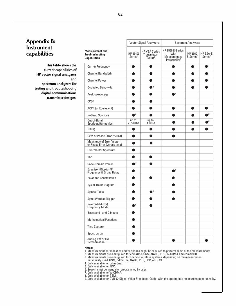
62
Appendix B:Instrument capabilities
Carrier Frequency
Channel Bandwidth
Channel Power
Occupied Bandwidth
Peak-to-Average
CCDF
ACPR (or Equivalent)
In-Band Spurious
Out-of-BandSpurious/Harmonics
Timing
EVM or Phase Error (% rms)
Magnitude of Error Vector or Phase Error (versus time)
Error Vector Spectrum
Rho
Code-Domain Power
Equalizer (Bits-to-RF Frequency & Group Delay
Polar and Constellation
Eye or Trellis Diagram
Symbol Table
Sync. Word as Trigger
Inverted (Mirror)Frequency Mode
Baseband I and Q Inputs
Mathematical Functions
Time Capture
Spectrogram
Analog PM or FM Demodulation
HP 89400Series1
HP VSA SeriesTransmitter
Tester2
HP 8590 E-Series with
Measurement Personality3
HP 8560 E-Series1
HP ESA-E Series1
up to 2.65 GHz6
up to 4 GHz6
6
6
5
4
6
Vector Signal Analyzers Spectrum Analyzers
Measurement andTroubleshootingCapabilities
6
7
8
9
Notes:1. Measurement personalities and/or options might be required to perform some of the measurements.2. Measurements pre-configured for cdmaOne, GSM, NADC, PDC, W-CDMA and cdma2000. 3. Measurements pre-configured for specific wireless systems, depending on the measurement
personality used: GSM, cdmaOne, NADC, PHS, PDC, or DECT. 4. Only available for cdmaOne.5. Only available for PDC.6. Search must be manual or programmed by user.7. Only available for W-CDMA.8. Only available for GSM.9. Only available for DVB-C (Digital Video Broadcast-Cable) with the appropriate measurement personality.
This table shows the current capabilities of
HP vector signal analyzersand
spectrum analyzers for testing and troubleshooting
digital communicationstransmitter designs.

3G . . . . . . . . . . . . . . . . . . . . . . . . . . . . . . . . . . . . . . . . . . . . . . . Third GenerationACP . . . . . . . . . . . . . . . . . . . . . . . . . . . . . . . . . . . . . . . Adjacent Channel Power ACPR . . . . . . . . . . . . . . . . . . . . . . . . . . . . . . . . . Adjacent Channel Power Ratiobits-to-RF frequency response . . . . . . Frequency response from baseband
to RF, using bits as the stimulus signal BW . . . . . . . . . . . . . . . . . . . . . . . . . . . . . . . . . . . . . . . . . . . . . . . . . . . . BandwidthCCDF . . . . . . . . . . . . . . . . Complementary Cumulative Distribution FunctionCDMA . . . . . . . . . . . . . . . . . . . . . . . . . . . . . . . . . Code Division Multiple AccesscdmaOne. . . . . . . . . . . . . . . . . . . . . . . . . . IS-95 standard-based CDMA systemcdma2000 . . . . . . . . . . . . . . . . . . . . . . . . . . . . cdmaOne derivative, 3G systemCMOS . . . . . . . . . . . . . . . . . . . . . Complementary Metal Oxide SemiconductorDAC . . . . . . . . . . . . . . . . . . . . . . . . . . . . . . . . . . . . . Digital-to-Analog ConverterDECT . . . . . . . . . . . . . . . . . . . . . . . . . . . Digital Enhanced Cordless TelephoneDSP . . . . . . . . . . . . . . . . . Digital Signal Processor or Digital Signal ProcessingDVB-C . . . . . . . . . . . . . . . . . . . . . . . . . . . . . . . . Digital Video Broadcast - CableEVM . . . . . . . . . . . . . . . . . . . . . . . . . . . . . . . . . . . . . . . . Error Vector MagnitudeFFT . . . . . . . . . . . . . . . . . . . . . . . . . . . . . . . . . . . . . . . . . Fast Fourier TransformFIR . . . . . . . . . . . . . . . . . . . . . . . . . . . . . . . . . . . . . . . . Finite Impulse ResponseFM . . . . . . . . . . . . . . . . . . . . . . . . . . . . . . . . . . . . . . . . . . Frequency Modulationframe . . . . . . . . . . . . . . . . . . . . . . In TDMA systems, a repeating time interval
divided among multiple users (see timeslot) GSM. . . . . . . . . . . . . . . . . . . . . . . . . Global System for Mobile communicationsGMSK. . . . . . . . . . . . . . . . . . . . . . . . . . . . . . . . Gaussian Minimum Shift KeyingIF . . . . . . . . . . . . . . . . . . . . . . . . . . . . . . . . . . . . . . . . . . Intermediate FrequencyI/Q . . . . . . . . . . . . . . . . . . . . . . . . . . . . . . . . . . . . . . . . . . . . In-phase/QuadratureISI . . . . . . . . . . . . . . . . . . . . . . . . . . . . . . . . . . . . . . . . Intersymbol InterferenceLMDS . . . . . . . . . . . . . . . . . . . . . . . . . . . . Local Multipoint Distribution SystemLO . . . . . . . . . . . . . . . . . . . . . . . . . . . . . . . . . . . . . . . . . . . . . . . . Local OscillatorMSB . . . . . . . . . . . . . . . . . . . . . . . . . . . . . . . . . . . . . . . . . . . Most Significant BitNADC. . . . . . . . . . . . . . . . . . . . . . . . . . North American Digital Cellular systemOQPSK . . . . . . . . . . . . . . . . . . . . . . . . . . Offset Quadrature Phase Shift KeyingORFS . . . . . . . . . . . . . . . . . . . . . . . . . . . . . . . . . . . . . . . . . Output RF Spectrum PA . . . . . . . . . . . . . . . . . . . . . . . . . . . . . . . . . . . . . . . . . . . . . . . . Power AmplifierPDC . . . . . . . . . . . . . . . . . . . . . . . . . . . . . . . . . . . Pacific Digital Cellular systemPHS . . . . . . . . . . . . . . . . . . . . . . . . . . . . . . . . . . . Personal Handyphone SystemPM . . . . . . . . . . . . . . . . . . . . . . . . . . . . . . . . . . . . . . . . . . . . . . Phase ModulationRF . . . . . . . . . . . . . . . . . . . . . . . . . . . . . . . . . . . . . . . . . . . . . . . Radio FrequencySA . . . . . . . . . . . . . . . . . . . . . . . . . . . . . . . . . . . . . . . . . . . . . Spectrum Analyzer SAW . . . . . . . . . . . . . . . . . . . . . . . . . . . . . . . . . . . . . . . . . Surface Acoustic Wave TDMA . . . . . . . . . . . . . . . . . . . . . . . . . . . . . . . . . Time Division Multiple Accesstimeslot . . . . . . . . . . . . . . . . . . . In TDMA systems, amount of time per frame
each mobile has to transmit information (see frame)VSA . . . . . . . . . . . . . . . . . . . . . . . . . . . . . . . . . . . . . . . . . Vector Signal Analyzer Walsh code . . Orthogonal code used in cdmaOne systems for channelization
in the forward link and as orthogonal modulation in the reverse link.W-CDMA . . . . . . . . . . . . . . . . . . . . . . . . . . . . . . . . Wideband CDMA, 3G system
63
5. Glossary

6. References
[1] Digital Modulation in Communications Systems, HP Application Note 1298, literature number 5965-7160E.
[2] Understanding CDMA Measurements for
Base Stations and Their Components, HP Application Note 1311, literature number 5968-0953E.
[3] Understanding GSM Transmitter Measurements for
Base Transceiver Stations and Mobile Stations, HP Application Note 1312, literature number 5968-2320E.
[4] Understanding PDC and NADC Transmitter
Measurements for Base Transceiver Stations and
Mobile Stations, HP Application Note 1324, literature number 5968-5537E.
[5] Testing and Troubleshooting Digital
RF Communications Receiver Designs, HP Application Note 1314, literature number 5968-3579E.
[6] Power Statistics of Digitally Modulated Signals, Pete Watridge,Wireless Symposium, 1999.
[7] Adaptive Equalization and Modulation Quality, Bob Cutler, Hewlett-Packard Wireless R&D Seminar, 1997.
[8] Spectrum Analyzer Measurements and Noise, HP Application Note 1303, literature number 5966-4008E.
7. Related Literature
1. Using Vector Modulation Analysis in the Integration,
Troubleshooting and Design of Digital RF
Communications Systems, HP Product Note 89400-8, literature number 5091-8687E.
2. Using Error Vector Magnitude Measurements to Analyze
and Troubleshoot Vector-Modulated Signals, HP Product Note 89400-14, literature number 5965-2898E.
3. HP 89400 Series Vector Signal Analyzers, literature number 5965-8554E.
4. HP VSA Series Transmitter Tester, literature number 5966-4762E.
5. HP 8560 E-Series Spectrum Analyzers, literature number 5966-3559E.
6. HP 8590 E-Series Spectrum Analyzers, literature number 5963-6908E.
7. HP ESA-E Series Spectrum Analyzers, literature number 5968-3278E.
For more information about
Hewlett-Packard test and measurement
products, applications and services,
and for a current sales office listing,
visit our web site, http://www.tmo.hp.com.
You can also contact one of the following
centers and ask for a test and
measurement sales representative.
United States:
Hewlett-Packard CompanyTest and Measurement Call CenterP.O. Box 4026Englewood, CO 80155-40261 800 452 4844
Canada:
Hewlett-Packard Canada Ltd.5150 Spectrum WayMississauga, Ontario L4W 5G1(905) 206 4725
Europe:
Hewlett-PackardEuropean Marketing CentreP.O. Box 9991180 AZ AmstelveenThe Netherlands(31 20) 547 9900
Japan:
Hewlett-Packard Japan Ltd.Measurement Assistance Center9-1, Takakura-Cho, Hachioji-Shi,Tokyo 192, JapanTel: (81) 426-56-7832Fax: (81) 426-56-7840
Latin America:
Hewlett-PackardLatin American Region Headquarters5200 Blue Lagoon Drive, 9th FloorMiami, Florida 33126, U.S.A.(305) 267 4245/4220
Australia/New Zealand:
Hewlett-Packard Australia Ltd.31-41 Joseph StreetBlackburn, Victoria 3130, Australia1 800 629 485
Asia Pacific:
Hewlett-Packard Asia Pacific Ltd.17-21/F Shell Tower, Times Square,1 Matheson Street, Causeway Bay,Hong KongTel: (852) 2599 7777Fax: (852) 2506 9285
Data Subject to Change
Copyright© 1999
Hewlett-Packard Company
Printed in U.S.A. 7.99
5968-3578E
![EGI - Governo e Strategie di Impresa [modalità compatibilità]webuser.unicas.it/madi/polese/uploads/EGI - Governo e Strategie di... · Catena del Valore Non correlata Correlata IDE](https://img.dokumen.tips/doc/110x75/5c65757009d3f2b26e8cb9ab/egi-governo-e-strategie-di-impresa-modalita-compatibilita-governo-e-strategie.jpg)


