Embed Size (px)
Citation preview
Testing and Hardness Assurance Guidelines for Single Event Transients (SETs) in Linear Devices
Prepared by: Christian Poivey, Stephen Buchner, Jim Howard, and Ken LaBel
NASA Goddard Space Flight Center (NASA/GSFC)
Ron Pease RLP Research
For: NASA Electronic Parts and Packaging (NEPP) Program Electronics Radiation Characterization (ERC) Project
And
Defense Threat Reduction Agency (DTRA)
October 24, 2005

2
Table of Contents 1 Introduction............................................................................................................................................. 3 2 Single Event Transients in Linear Devices: Lessons Learned ................................................................ 3
2.1 Introduction..................................................................................................................................... 3 2.2 Heavy-Ion Induced SETs ................................................................................................................ 5 2.3 Proton-Induced SETs ...................................................................................................................... 8 2.4 Effect of Bias Conditions ................................................................................................................ 8
2.4.1 Introduction............................................................................................................................. 8 2.4.2 Effect of Input Bias on Device Sensitivity.............................................................................. 8 2.4.3 Effect of Power Supply on Device SET Sensitivity................................................................ 9 2.4.4 Effect of Bias Conditions on SET Characteristics ................................................................ 10 2.4.5 Effect of the Load ................................................................................................................. 11
2.5 Test Set-up .................................................................................................................................... 13 2.6 Data Analysis and Reporting ........................................................................................................ 14 2.7 SET Rate Prediction...................................................................................................................... 14
3 Assessment of Single Event Transient Sensitivity................................................................................ 16 3.1 Introduction................................................................................................................................... 16 3.2 Testing Guidelines for Evaluation SET Sensitivity ...................................................................... 16
3.2.1 Introduction........................................................................................................................... 16 3.2.2 Irradiation Conditions ........................................................................................................... 17 3.2.3 Test Samples ......................................................................................................................... 18 3.2.4 Bias Conditions ..................................................................................................................... 19 3.2.5 Test Set-up ............................................................................................................................ 19 3.2.6 Data Analysis and Reporting ................................................................................................ 20
3.3 SET Rate Prediction Guideline ..................................................................................................... 20 3.4 Laser Testing and Simulation ....................................................................................................... 21
3.4.1 Introduction........................................................................................................................... 21 3.4.2 Laser Testing......................................................................................................................... 21 3.4.3 Simulation ............................................................................................................................. 23
4 Design Guidelines................................................................................................................................. 23 4.1 Introduction................................................................................................................................... 23 4.2 Device Descriptions ...................................................................................................................... 23
4.2.1 Voltage Comparators ............................................................................................................ 23 4.2.2 Operational Amplifiers ......................................................................................................... 23 4.2.3 Voltage References ............................................................................................................... 24 4.2.4 Voltage Regulators................................................................................................................ 24 4.2.5 MOSFET Drivers.................................................................................................................. 24 4.2.6 Analog-to-Digital/Digital-to-Analog Converters (ADC/DAC)............................................. 24 4.2.7 Line Drivers/Receivers/Transceivers .................................................................................... 24 4.2.8 Sample and Hold Amplifiers................................................................................................. 24 4.2.9 Timers ................................................................................................................................... 24 4.2.10 Pulse Width Modulators (PWM) .......................................................................................... 25 4.2.11 Hybrid Devices ..................................................................................................................... 25
5 Hardness assurance ............................................................................................................................... 26 5.1 Introduction................................................................................................................................... 23 5.2 Generic piece-part hardness assurance.......................................................................................... 23 5.3 Linear circuit SET piece-part hardness assurance......................................................................... 23
5.3.1 RDM for linear circuit SET................................................................................................... 23 5.3.2 Establishing a failure definition ............................................................................................ 29 5.3.3 Characterizing the SET response of the linear circuit ........................................................... 30 5.3.4 Calculating the RDM ............................................................................................................ 31 5.3.5 Categorization ....................................................................................................................... 32 5.3.6 Lot acceptance testing........................................................................................................... 33
5.4 Concluding remarks on hardness assurance.................................................................................. 34 6 References............................................................................................................................................. 35

3
1 Introduction A Single Event Transient (SET), also known as an Analog Single Event Upset (ASEU), in a linear device is caused by the generation of charge by a single particle (proton or heavy ion) passing through a sensitive node in the linear circuit. The SET consists of a transient voltage pulse generated at that node that propagates to the device output, where it appears as the same voltage transient, an amplified version of this transient, or a change in the logical output (e.g., in an Analog to Digital Converter (ADC). SETs or ASEUs in linear devices were first identified following an in-flight anomaly in the TOPEX POSEIDON spacecraft [1]. Since that event, SETs have been identified as the cause of several anomalies on multiple satellites including SOHO [2, 3], Cassini [4], MAP [5], and TDRS. Because of the large number of linear components used in spacecraft, this phenomenon is a significant problem. SETs in analog circuits are now an important issue for the design and development of space electronics. This document is intended to provide guidelines for the risk assessment of SETs in satellite applications and to recommend ground test protocols. These guidelines are based on many man-years of SET testing at both accelerator and pulsed laser facilities by NASA/GSFC personnel and other members of the Defense Threat Reduction Agency (DTRA) analog SET working group including NAVSEA Crane, Naval Research Laboratories (NRL), RLP Research, and Vanderbilt University. This guide is targeted towards both the design engineer and the radiation effects engineer. It is based on the assumption that the radiation effects expert has a working knowledge of the practices outlined in the two Single Event Effect (SEE) testing guidelines documents listed below:
1. ASTM Guide F1192-00-Standard Guide for the Measurement of Single Event Phenomena (SEP) Induced by Heavy Ion Irradiating of Semiconductor Devices.
2. JEDEC 57 Heavy Ion Testing Guideline.
2 Single Event Transients in Linear Devices: Lessons Learned
2.1 Introduction SETs have been observed in many different types of linear microcircuits such as operational amplifiers, voltage references, voltage comparators, ADCs, and others [1-12]. A general description of SEE effects on the different types of linear microcircuits is provided in Section 4 of this document. SETs in linear devices differ significantly from other types of Single Event Effects (SEE), such as, for example, Single Event Upset (SEU) in a memory. Each SET has its unique characteristics (polarity, waveform, amplitude, duration) depending on ion or proton impact location, ion or proton energy, device bias condition, and output load. On a single device, a large variety of SET waveforms can be obtained. For example, Figs. 1 to 4 show the dominant classes of SETs that have been obtained on the LM124 operational amplifier from National Semiconductor [13, 14]:
• Large-amplitude, positive-going transients with fast recovery times in Fig. 1. • Small and large amplitude, positive-going transients with slow recovery times in Fig. 2. • Negative-going transients with slow recovery times (small and large amplitude) in Fig. 3. • Positive- and negative-going transients with small amplitude and small duration in Fig. 4.
Linear devices are unique because they can be used in a large variety of bias and input conditions. Moreover, bias conditions significantly impact both the device SET sensitivity and the SET characteristics. Examples are given in Section 2.4.

4
Fig. 1. Example of large-amplitude, fast recovery time, positive-going transient.
Fig. 2. Example of small-amplitude, positive-going transients with slow recovery times.
5
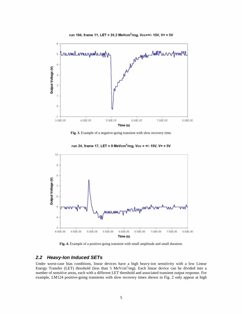
Fig. 3. Example of a negative-going transient with slow recovery time.
Fig. 4. Example of a positive-going transient with small amplitude and small duration.
2.2 Heavy-Ion Induced SETs Under worst-case bias conditions, linear devices have a high heavy-ion sensitivity with a low Linear Energy Transfer (LET) threshold (less than 5 MeVcm2/mg). Each linear device can be divided into a number of sensitive areas, each with a different LET threshold and associated transient output response. For example, LM124 positive-going transients with slow recovery times shown in Fig. 2 only appear at high

6
LET. SET waveform and characteristics (amplitude, duration) vary with LET. Fig. 5 and Fig. 6 show examples of the effect of LET on two LM124 transient waveforms.
Fig. 5. Effect of LET on amplitude of LM124 negative-going transients with slow recovery time.
Fig. 6. Effect of LET on amplitude and duration of large-amplitude,
positive-going transients with fast recovery times. Fig. 7 shows a schematic cross-section of the different types of transistors used in linear integrated circuits: vertical NPN, substrate PNP, and lateral PNP. We can see in the figure three main charge collection regions. The first region resides at the base/collector junctions in the lateral PNP transistors, the base/emitter and base/collector junctions of the NPN transistors, and in the base/emitter junctions of the

7
substrate PNP transistors. The second charge collection region resides at the base/collector junction of the substrate PNP and base/emitter junction of lateral PNP transistors. The third charge collection region resides at the buried layer/substrate junction in the lateral PNP and NPN transistors. For the devices currently used and tested, which were designed in the nineteen eighties, the first charge collection region is approximately 7 to 8 µm deep, the second is approximately 18 to 20 µm deep, and the third is approximately 28 to 30 µm deep. For low voltage state-of-the-art bipolar linear devices and CMOS linear devices, the depths of interest may be much less. When low-energy, short-range ions are used, especially when SET measurements are made with ions at non-normal incidence, the ions may not reach the device’s deepest sensitive regions. Or when they do, their energies may be so low that the LET and effective LET concept are no longer valid.
n+ n+
n+
p
n-epip+p+
p-substrat
Collector Emitter Base
a) Vertical NPN
Oxide
n-epip+p+
p-substrat (collector)
Emitter Base
b) Substrate PNP
pn+
Oxide
n+
n-epip+p+
p-substrat
CollectorEmitter Base
b) Lateral PNP
p pn+
Oxide
n+ n+
n+
p
n-epip+p+
p-substrat
Collector Emitter Base
a) Vertical NPN
Oxide
n-epip+p+
p-substrat (collector)
Emitter Base
b) Substrate PNP
pn+
Oxide
n+
n-epip+p+
p-substrat
CollectorEmitter Base
b) Lateral PNP
p pn+
Oxide
Fig. 7. Schematic cross-section of transistors used in linear devices.
For example, Fig. 8 shows the LM111 SET cross-section versus LET [15]. The data points are color coded with black representing ions with a range of 18 µm and red representing ions with a range of 200 µm. The figure shows that at high LET the measurements made with the low range ions underestimate the device’s SET cross section by about one order of magnitude. This clearly demonstrates that an ion with an 18-µm range is not sufficient for an adequate characterization of this device.
LET (MeV/mg/cm2)0 20 40 60 80 100
Cro
ss S
ectio
n (c
m2 )
1e-6
1e-5
1e-4
1e-3
1e-2
TAMU Data
BNL 02 Data
LM111
Fig. 8. LM111 SET cross-section versus LET. Short range ions (18 µm) are in black. Long range ions (200 µm) are in
red. All the data shown here are for an angle of incidence of 0 degrees [15].

8
2.3 Proton-Induced SETs Most of the SET data available in the literature for linear devices were obtained using heavy ions. Those data reveal very low heavy-ion SET LET thresholds, which suggest that linear devices will also exhibit a significant sensitivity to proton-induced SETs. Yet, very little proton data are available. Proton data on the LM139 voltage comparator [3, 8], for example, confirm this proton sensitivity, but only for low-input differential voltages (<100 mV). Proton-induced SET sensitivity is also reported for pulse-width modulator (PMW) devices and power-supply devices [3]. Direct ionization from protons does not cause SETs in bipolar linear devices. Proton-induced SET cross-sections for high-energy protons (>200 MeV) are six to seven orders of magnitude smaller than the saturated heavy-ion SET cross-sections, and energy thresholds are greater than 30 MeV. This is consistent with ionizing radiation deposition due to the reaction products from proton interaction with device lattice nuclei.
2.4 Effect of Bias Conditions
2.4.1 Introduction Both the sensitivity and waveform characteristics of SETs in linear devices depend on the device bias conditions. The following paragraphs show some examples for voltage comparators and operational amplifiers.
2.4.2 Effect of Input Bias on Device Sensitivity Fig. 9 shows an example for the LM139 voltage comparator from National Semiconductor (NSC). The figure clearly shows the effect of ∆Vi on the LET threshold. Other voltage comparators show less effect of ∆Vi on SET sensitivity, but in all cases the lowest ∆Vi gives the highest SET sensitivity [8-11].
Fig. 9. LM139 NSC SET cross-section curves for different values of differential input voltage [4, 16].
Fig. 10 shows the SET cross-section curves of the LM124 operational amplifier for different bias configurations. One remarkable result is that all conditions, no matter how different, give similar cross-section results as long as the nominal device’s output voltage is not too close to a power supply voltage rail. When the nominal device’s output is too close to a power supply rail, as is the case for the inverting

9
gainx10 application with a 1V input voltage, the SET sensitivity is significantly reduced. Test data on other operational amplifiers show similar results [17-19].
Fig. 10. LM124 NSC SET cross section curves for different bias conditions [13].
2.4.3 Effect of Power Supply on Device SET Sensitivity No significant effects of power supply were observed on the LM139 SET sensitivity [14, 16]. NASA/GSFC and NAVSEA/CRANE test data on LM124, collected for different power supply voltages show similar SET sensitivity [13, 20]. However, the device output voltage gets closer to the supply-voltage rails when the power-supply voltage is reduced, and this may have an impact on the SET sensitivity. For example, Fig. 11 shows the SET cross-sections of the LM124 operational amplifier in a non-inverting gain x101 application for two different power supply voltages. The sensitivity is significantly higher for a power supply voltage of +/-15V than for a power supply voltage of +5/0V.
Fig. 11. LM124 SET cross-section curve for different bias conditions [14].
10
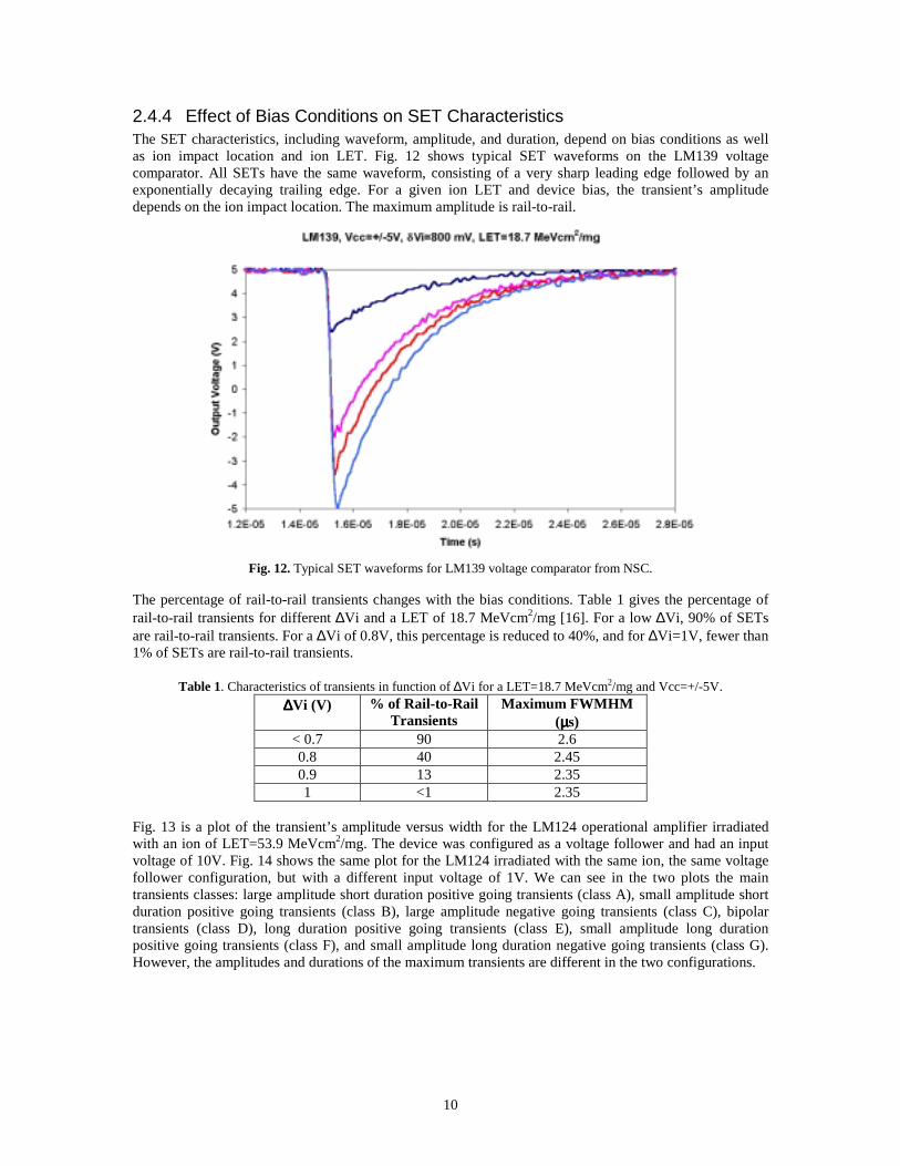
2.4.4 Effect of Bias Conditions on SET Characteristics The SET characteristics, including waveform, amplitude, and duration, depend on bias conditions as well as ion impact location and ion LET. Fig. 12 shows typical SET waveforms on the LM139 voltage comparator. All SETs have the same waveform, consisting of a very sharp leading edge followed by an exponentially decaying trailing edge. For a given ion LET and device bias, the transient’s amplitude depends on the ion impact location. The maximum amplitude is rail-to-rail.
Fig. 12. Typical SET waveforms for LM139 voltage comparator from NSC.
The percentage of rail-to-rail transients changes with the bias conditions. Table 1 gives the percentage of rail-to-rail transients for different ∆Vi and a LET of 18.7 MeVcm2/mg [16]. For a low ∆Vi, 90% of SETs are rail-to-rail transients. For a ∆Vi of 0.8V, this percentage is reduced to 40%, and for ∆Vi=1V, fewer than 1% of SETs are rail-to-rail transients.
Table 1. Characteristics of transients in function of ∆Vi for a LET=18.7 MeVcm2/mg and Vcc=+/-5V. ∆∆∆∆Vi (V) % of Rail-to-Rail
Transients Maximum FWMHM
(µµµµs) < 0.7 90 2.6 0.8 40 2.45 0.9 13 2.35 1 <1 2.35
Fig. 13 is a plot of the transient’s amplitude versus width for the LM124 operational amplifier irradiated with an ion of LET=53.9 MeVcm2/mg. The device was configured as a voltage follower and had an input voltage of 10V. Fig. 14 shows the same plot for the LM124 irradiated with the same ion, the same voltage follower configuration, but with a different input voltage of 1V. We can see in the two plots the main transients classes: large amplitude short duration positive going transients (class A), small amplitude short duration positive going transients (class B), large amplitude negative going transients (class C), bipolar transients (class D), long duration positive going transients (class E), small amplitude long duration positive going transients (class F), and small amplitude long duration negative going transients (class G). However, the amplitudes and durations of the maximum transients are different in the two configurations.

11
Fig. 13. LM124, transient amplitude versus width plot, LET=53.9 MeVcm2/mg, Voltage follower, Vin=10V.
Fig. 14. LM124, transient amplitude versus width plot,
LET=53.1 MeVcm2/mg, Voltage follower, Vin=1V.
2.4.5 Effect of the Load The device output load can also have an effect on the transient characteristics (amplitude and duration). An example is given in Fig. 15 for the LM139 voltage comparator. Fig. 15 shows the typical rail-to-rail transient waveform for identical input bias conditions and LET and different values of pull-up resistors. A direct relationship is seen between the pull-up resistor value and the duration of the transient exponential decay.

12
Fig. 15. LM139, typical rail to rail transient for two different values of the pull-up resistor
(∆Vin=0.1V, LET=11.4 MeVcm2/mg). In case of large capacitive loads, small amplitude transients may be filtered. For example, Fig. 16 shows the LM124 SET cross-sections measured at TEXAS A&M with low capacitance FET probes and at BNL with regular probes and a long connection between the device under test and the oscilloscope because of the vacuum chamber. We can see the large difference, about one order of magnitude, between the two measurement conditions.
Fig. 16. LM124, comparison of the SET cross section measured at TAMU and BNL. At TAMU data were taken in air using short connection and low capacitance FET probes between the device under test and the
oscilloscope. At BNL data were taken in the vacuum chamber using long connection, to go through the vacuum feedthrough, and regular probes between the device under test and the oscilloscope.
13
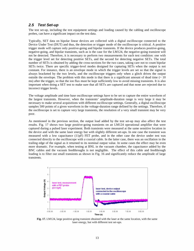
2.5 Test Set-up The test set-up, including the test equipment settings and loading caused by the cabling and oscilloscope probes, can have a significant impact on the test data. Typically, SET data on bipolar linear devices are collected with a digital oscilloscope connected to the Device Under Test (DUT) and thus, the detection or trigger mode of the oscilloscope is critical. A positive trigger mode will capture only positive-going and bipolar transients. If the device produces positive-going, negative-going, and bipolar transients, such as is the case for the LM124, the negative-going transient will not be detected. Therefore, it is necessary to perform two measurements for each test condition: one with the trigger level set for detecting positive SETs, and the second for detecting negative SETs. The total number of SETs is obtained by adding the cross-sections for the two cases, taking care not to count bipolar SETs twice. There are specific trigger-level modes designed for capturing SETs when the output is not constant. For instance, there is an envelope mode in which the trigger levels are set so that the signal is always bracketed by the two levels, and the oscilloscope triggers only when a glitch drives the output outside the envelope. The problem with this mode is that there is a significant amount of dead time (~ 10 ms) after the trigger, so that the ion flux must be kept sufficiently low to avoid missing transients. It is also important when doing a SET test to make sure that all SETs are captured and that none are rejected due to incorrect trigger levels. The voltage amplitude and time base oscilloscope settings have to be set to capture the entire waveform of the largest transients. However, when the transients’ amplitude-duration range is very large it may be necessary to make several acquisitions with different oscilloscope settings. Generally, a digital oscilloscope samples 500 points of a given waveform in the voltage-duration range defined by the settings. Therefore, if the oscilloscope is set to capture very large transients, the resolution of a very small transient may be very poor. As mentioned in the previous section, the output load added by the test set-up may also affect the test results. Fig. 17 shows two large positive-going transients on an LM124 operational amplifier that were captured during a pulsed laser experiment. Both transients were measured at the same sensitive location in the device and with the same laser energy but with slightly different set-ups. In one case the transient was measured with a low capacitance (11pF) FET probe, and in the other case the device under test was connected directly to the oscilloscope with a coaxial cable. In the latter case, there was an oscillation in the trailing edge of the signal as it returned to its nominal output value. In some cases the effect may be even more dramatic. For example, when testing at BNL in the vacuum chamber, the capacitance added by the BNC cables and the vacuum feedthroughs is not negligible. The effect of this cable and feedthrough loading is to filter out small transients as shown in Fig. 16 and significantly reduce the amplitude of large transients.
Fig. 17. LM124, large positive-going transient obtained with the laser at the same location, with the same
laser energy, but with different test set-ups.

14
2.6 Data Analysis and Reporting The discussion of section 2.5 demonstrates the complexity of SET testing due to the large variety of SET responses that depend on bias and irradiation conditions. This results in the need to collect a comprehensive set of test data reflecting different operating conditions in order to understand the device behavior and bound the part response for each possible application [14]. It is often necessary to test a linear device for SET in the bias condition of a specific application to understand and mitigate the SET effects for that particular application. This requires that several sets of test data be obtained for different applications for the same device. Because of the large amount of data collected during SET testing, it is not possible to summarize all the information in a test report. Generally, only test data for the device worst-case response need be presented. This means that for each tested condition, the total number of detected SETs should be reported. However, this worst-case data may not be sufficient to assess the SET criticality for a specific application. Fig. 18 shows the SET cross-section curve of a PM139 voltage comparator from Analog Devices for a ∆Vi of 1V. The blue curve represents the cross-section curve for the transients of amplitude larger than 0.5V [10]. The magenta curve is the cross-section curve for the transients of amplitude critical for a specific application. For the same bias conditions, the worst-case SET cross-section for a specific application may significantly overestimate the device sensitivity. Therefore, it is necessary to collect all the transients during an experiment and to store them for further analysis at a later date.
Fig. 18. LM139 from Analog Devices, SET cross-section curves for δVi=1V. The blue curve is the cross-section curve for all transients of amplitude > 0.5V. The magenta curve is the cross-section
curve of the transients critical for the application.
2.7 SET Rate Prediction There are numerous sources of uncertainty in the calculation of SET rates in linear devices operating in space. The first one is the uncertainty in the environment which is not specific to SETs in linear devices. The authors of CREME 96 estimate the accuracy of the Galactic Cosmic Rays (GCR) model at about 25%. It is not possible to estimate the accuracy of the CREME96 Solar Particle Event (SPE) model, but it is generally considered that these models give a reasonably conservative estimate of the event rates during a solar particle event [21]. The assumptions on the shielding generally do not have a significant impact when considering the GCR, but their impact is significant when considering SPE [5].

15
The second one is the uncertainty of the SET cross-section curve that may be significant and impact the calculated SET rates by orders of magnitude. The main uncertainty is the definition of the SET curve for the specific application bias conditions. When the part is tested in the application conditions and when the critical transient criteria for this particular application are well defined, the accuracy of the cross-section measurement and the LET threshold definition may result in a factor of two errors in the error rate. There are also the uncertainties of the sensitive volume. Laser testing on LM139 and LM124 [11, 14, 22] allowed identification of different sensitive areas. SET rate calculations on linear devices assume generally only one sensitive volume. This assumption will give a conservative estimate of the SET rate. Table 2 shows the effect of the number of sensitive volumes on the predicted SET rate of a LM139 for a geostationary orbit. For these geometries the assumption of the number of sensitive volumes does not change the GCR induced rate significantly but does change the SPE induced rate by about one order of magnitude. The analysis of linear devices has also shown that the different sensitive nodes have different thickness and some sensitive junctions can be very deep [10, 15, 20, 23]. Assuming a sensitive volume thickness of 2 µm will give a conservative estimate of the SET rate. Table 3 shows the effect of sensitive volume thickness on the predicted SET rate of a LM139 for a geostationary orbit. For these geometries the assumption on the sensitive volume thickness changes the GCR induced rate by less than a factor 2 and changes the SPE induced rate by more than one order of magnitude.
Table 2: Variation of LM139 SET rate in a geostationary orbit for different assumptions on the number of sensitive
volumes- ∆Vi=200 mV, Leth=4.5 MeVcm2/mg, Xsat=6E-4 cm2/comparator, thickness of sensitive volume Z=2 um, 200 mils of Al shielding.
Number of Sensitive
Nodes
Sensitive Node Area
[µµµµm2]
Rate of GCR Induced SET (CREME96 solmin)
[event/comparator-day]
Rate of SPE Induced SET (CREME96 worst day) [event/comparator-day]
1 60000 4.99E-03 1.63E+00 10 6000 4.83E-03 7.84E-01
100 600 4.34E-03 2.17E-01
Table 3: Variation of LM139 SET rate in a geostationary orbit for different assumptions on the thickness of the sensitive volume- ∆vi=200 mV, LETth=4.5 MeVcm2/mg, Xsat=6E-4 cm2/comparator,
one sensitive volume, 200 mils of Al shielding. Sensitive Volume
Thickness [µµµµm]
Rate of GCR Induced SET (CREME96 solmin)
[event/comparator-day]
Rate of SPE Induced SET (CREME96 worst day) [event/comparator-day]
2 4.99E-03 1.63E+00 5 4.88E-03 9.40E-01
10 4.69E-03 5.10E-01 15 4.51E-03 3.20E-01 20 4.34E-03 2.10E-01 30 4.02E-03 1.30E-01 40 3.70E-03 1.20E-01 60 3.01E-03 9.83E-02
Comparisons between predicted and actual flight data are rare because no SET experimental data are available; the in-flight anomalies are generally not published, and the number of observed events is not statistically significant. The only flight data available are from SOHO, where the observed anomalies have been reproduced at ground level and the parts characterized in the actual application conditions [2-3]. Table 4 compares the observed rates in flight to the predicted rates. A fairly good correlation is observed.

16
Table 4: Number of observed SET on SOHO in 5 years, and comparison with the calculated rates. Assumptions for the calculation: CREME96 GCR solmax model, 1 g/cm2 of shielding, one sensitive volume of area the saturated cross-
section/device and a thickness of 2 µm [2, 3]. Module Device Observed in
Flight Predicted
VIRGO PM139 5 5 LASCO UC1707 0 ~0.1
ACU UC1707 5 3
3 Assessment of Single Event Transient Sensitivity
3.1 Introduction A transient pulse from a linear device can propagate through follow-on circuits and cause failures in flight hardware and systems. False information potentially generated by an analog SEU in flight hardware should be taken into account if the impact is at the system level, especially if the function being performed is deemed critical (equipment reset, shutdown, etc.). The study of and hardening to such events is a three-step process. First, a description of the consequences of SETs at the equipment level must be made. Secondly, an analysis of the SET impact at the subsytem and system levels, and identification of critical events and acceptable rates, need to be developed. Finally, any required mitigation of critical events at system/subsystem or equipment level must be implemented. SET analysis is similar to the criticality analysis process described in the NASA GSFC SEE Criticality Analysis (SEECA) document [24] for other SEE effects; however, it is more complex because of the dependence of device SET sensitivity on application and the large variety of transients’ characteristics. In the ideal case, SET mitigation has been designed into both the subsystem and the system at the beginning of the design process, and no radiation data are required. Design guidelines are provided in Section 4. In most cases SET radiation data on transient characteristics and transient event rates are necessary to assess the impact at the subsystem and system level. As seen in Section 2, variations of the input and bias conditions in a number of linear devices may dramatically change the event rate and the transient characteristics (peak heights and widths). This implies that either the radiation test data must be taken over a very large range of parameters, or application-specific testing must be done for each application of each device type. Alternative approaches to heavy-ion testing for each application condition are the use of an electrical SET model or a pulsed laser test [25].
3.2 Testing Guidelines for Evaluation SET Sensitivity
3.2.1 Introduction Testing integrated circuits (ICs) for SET sensitivity involves irradiating the ICs with heavy ions or protons at an accelerator facility to produce SETs that are captured and stored for subsequent analysis. The SET cross-section (number of SETs per unit particle fluence) and waveform characteristics (amplitude and width) are obtained as a function of ion LET (or proton energy). Although the experiment appears to be relatively straightforward, numerous factors must be considered if relevant and accurate data are to be obtained. Those factors may be divided into three broad categories: irradiation conditions, device configuration, and data acquisition equipment. The failure to address any of these factors could result in invalid or non-relevant data and a less than successful test trip. By being cognizant of all the issues associated with SET measurements, the radiation effects engineer increases the chances of successfully characterizing the SET response of ICs exposed to an ionizing particle environment.

17
3.2.2 Irradiation Conditions
3.2.2.1 Heavy Ions
3.2.2.1.1 Ion LET and Range The DUT should be tested with different ions over a range of LETs to get the full cross-section curve from the LET threshold to an LET where the SET cross-section saturates. The LET may be varied by changing ion species and/or energy or by changing the angle of incidence. However, the use of tilted beam must be used with care since the effects of varying the angle of incidence, to modify the LET, are complicated by the presence of sensitive junctions at depths well below the IC surface. Only ions with ranges exceeding the deepest junctions should be used. The range in silicon of an ion, which may be calculated using the program SRIM, should be a minimum of 50 µm. This will ensure that the Bragg peak is beyond the deepest SET sensitive junction and that the ion LET does not change appreciably across the junction even at non-normal incidence. In summary, ions should be selected for SET testing based on both their LET and their range.
3.2.2.1.2 Ion Beam Flux The selection of ion beam flux or equivalently beam current is determined by a number of factors. First, the maximum flux should not be so large that the SETs overlap in time precluding the measurement of amplitude and width. Avoiding overlap is especially important for long-duration SET pulses. For example, Fig. 19 shows the long duration transients, about 600 µs, which were observed in the OP293 operational amplifier.
Fig. 19. Long duration transients observed on the OP293 operational amplifier [26].
More than 10% of OP293 transients are long duration transients.
3.2.2.1.3 Ion Fluence The fluence, defined as the product of the flux and the exposure time, is determined primarily by statistics. Calculations of SET rates depend on obtaining an accurate representation of the SET cross-section as a

18
function of LET. Therefore, it is important that the error bars on the data points be as small as practicable. The uncertainty in the SET cross-section is determined by the number (N) of SETs measured and is proportional to N-0.5, which is one standard deviation. Therefore, for an uncertainty of 10% one needs to capture 100 SETs. However, the specificity of SET testing in linear devices is that different types of SET can be collected. In order to collect a significant number of all the different transient waveforms, capturing a minimum of 200 transients is recommended. Following the capture of the 200th SET or a maximum fluence of 106 ions/cm2, the accelerator ion beam must be turned off immediately and the total fluence noted.
3.2.2.1.4 Ion Beam Damage Exposure to high fluences of ions may result in significant Total Ionizing Dose (TID) damage that will affect the characterization results. Certain linear bipolar devices are very sensitive to TID. However, at high LET the effective dose is a small fraction of the actual dose and the dose is deposited at a high dose rate where the linear bipolar devices are less sensitive. We recommend that the cumulated dose does not exceed 80% of the device’s TID capability or 100 krad.
3.2.2.2 Protons
3.2.2.2.1 Proton Energy Protons do not generate sufficient charge via direct ionization to produce SETs in currently available linear circuits. Instead, SETs are generated via nuclear reactions involving either an elastic or inelastic collision between the proton and the nucleus of the semiconductor material. Because nuclear reaction cross-sections depend on proton energy, so do SET cross-sections, amplitudes, and widths. Ideally, measurements ought to be done at a number of different proton energies that span the energy range from 30 to 200 MeV.
3.2.2.2.2 Proton Fluence As for heavy ion testing, the fluence, defined as the product of the flux and the exposure time, is determined primarily by statistics, and to collect a significant number of all the different transient waveforms, capturing a minimum of 200 transients is recommended. Following the capture of the 200th SET or a maximum fluence of 1010 protons/cm2, the accelerator proton beam must be turned off immediately and the total fluence noted.
3.2.2.2.3 Proton Damage Exposures to high fluences of protons may result in significant Displacement Damage (DD) and TID that will affect the characterization results. Certain devices, such as the LM111, are more sensitive to DD/TID because of the lateral PNP transistors in the input part of the circuit. The LM111 was non-functional after a 63 MeV proton fluence of 3x10¹² protons/cm2. In contrast, the LM119, which has only vertical NPN transistors, was still functional after a 63 MeV proton fluence of 3x10¹³ protons/cm2, although the SET amplitude had decreased as a result of DD/TID. These fluence levels correspond to TID levels of about 400 krad(Si) and 4 Mrad(Si) respectively. Like for heavy ions, these high failure levels, compared to TID failure levels of these parts, can be explained by the fact that high energy protons have a high recombination yield and the dose is deposited at a very high dose rate. We recommend that the cumulated dose on each tested device does not exceed 80% of the device’s TID capability or 50 krad.
3.2.3 Test Samples
3.2.3.1 Sample selection The parts tested should be representative of those intended for the application to avoid the possibility of testing parts manufactured with a modified process that would affect the SET sensitivity. Generally process variations have less effect on SEE sensitivity than on TID sensitivity. Therefore, it is not necessary to test parts from the same diffusion lot than the flight lot. Test samples with the same mask and fabrication steps

19
than the flight parts will be representative of these flight parts. When no information is available about the design and process updates, like it is the case for commercial parts, test samples should be taken from the flight parts procurement lot.
3.2.3.2 Number of Parts As stated in JESD57, test sample size for SEE testing can be small. We recommend testing a minimum of two devices and increasing the sample size if a part to part dispersion is observed. In the case of commercial parts where no information is available about the homogeneity of the flight lot population, it is recommended to increase the sample size.
3.2.3.3 Use of Delidded Parts In most cases, heavy-ion testing will require the removal of any lids or plastic encapsulate because the heavy ions available at most accelerators do not have sufficient energy to penetrate the lids or plastic encapsulate. It is not necessary to delid ICs or remove any plastic encapsulate if high-energy protons are used to test for SET sensitivity. High-energy protons (> 30 MeV) will penetrate with little loss in energy.
3.2.4 Bias Conditions A large set of different bias conditions is necessary to understand and measure their effect on device sensitivity and transient characteristics [14]. This is why in most cases linear devices are tested in their application bias conditions. When a linear device must be tested in more than one voltage configuration, the experimental set-up should include the ability to change the voltages remotely to save time by avoiding having to enter the experimental area unnecessarily.
3.2.5 Test Set-up The transient characteristics change with irradiation conditions (ion LET or proton energy) and bias conditions. Therefore, the SETs at each LET should be captured and stored electronically to be able to analyze their characteristics for the different test conditions. The approach of choice is to capture SETs with an oscilloscope and to store the data on a computer hard drive. Analyzing the stored SETs provides information on their amplitude and width distributions. The oscilloscope’s trigger level should be set very low to capture all SETs. The equipment used to measure the SETs should have sufficient bandwidth to avoid distorting the waveforms. For example, large parasitic capacitances and resistances will reduce SET amplitude and increase pulse width. The best approach is to connect the IC’s output to an oscilloscope with an active probe having a low capacitance. The active probe is capable of driving the signal through a reasonably long cable. A passive probe may also be used, but the signal amplitude will decrease if connected via a long cable to the oscilloscope. At some accelerators, such as the Cyclotron Facility at Texas A&M, DUTs are mounted in air for exposure, and it is relatively simple to connect an oscilloscope to an IC’s output with an active probe. At other accelerators, such as the Tandem Van der Graaf at Brookhaven National Laboratory, the DUTs are mounted in a vacuum chamber. This requires connections through vacuum feedthroughs and results in long cables. The use of an active probe with its own power supply requires that special feedthroughs be assembled with the power supply either inside or outside the chamber.
SETs vary in amplitude and shape depending on ion LET and voltages and loads applied to the DUT. Some ICs, such as the voltage comparators, produce SETs with a single polarity; the response tends to be either a negative going transient for the high state or a positive going transient for the low state. Others, like operational amplifiers, produce positive going, negative going and bipolar SETs depending on which

20
transistor in the IC is struck by the ion. It is important when doing an ion test to make sure that all SETs are captured and that none are rejected because of incorrect trigger setting. One approach is to connect the IC output to two separate oscilloscope channels – one for positive and the other for negative SETs. This ensures that all SETs are captured, even those with bipolar waveforms. This solution is the preferred option at NASA/GSFC.
3.2.6 Data Analysis and Reporting Once the data are collected, an analysis is needed. For each application, only those SETs whose amplitudes and widths exceed minimum values, determined by the application, should be counted and analyzed. The cross-section is defined and the SET rate calculated for this specific application. Since it is generally not possible to analyze and report on all possible applications, it is important to store the data for possible future analysis. At minimum, the report should include:
• Bias conditions. • Measurement conditions (trigger levels). • Total cross-section curves for each tested bias conditions. • Traces of the different types of waveforms collected with worst-case characteristics (amplitude,
duration) and a description of how they contribute to the total cross-section curve. A discussion that gives an overview of the transient characteristics is a plot of transient amplitude versus width. An example is shown in Fig. 20 for the LM124.
Pulse Width (µµµµs)0 2 4 6 8 10 12 14
Am
plitu
de (V
olts
)
-4
-3
-2
-1
0
1
2
3
4
Slow Signal Decay TimeFast Signal Decay TimeGlitch
National LM124A0.65 Volts Bias
Fig. 20. SET amplitude versus duration, LM124, Non Inverting gain x2 application,Vin=0.65V [27].
3.3 SET Rate Prediction Guideline The following general guidelines are applicable for SET rate predictions:

21
• Use of appropriate radiation environment models (CREME96 for heavy ions and solar protons, AP8 for trapped protons) with the appropriate solar modulation (solar minimum or solar maximum).
• Use of an accurate shielding estimation to calculate the SET rates during SPE. • Use of an accurate heavy ion and proton characterization.
The unique aspect of SETs in linear devices is the presence of different sensitive regions of different size and thickness. Some of these sensitive regions can be very deep. It is difficult to know the exact number of sensitive areas, their dimensions, and the individual SET cross-section. Therefore, SET rates are generally calculated by assuming that there is one sensitive volume with an area equal to the SET device cross-section and a unique thickness. These assumptions will give a conservative estimate of the in-flight SET rate. The assumed value for the thickness of the sensitive volume will have a significant impact on the SET rate calculations. However, experience has led us to the assumption that a thickness of 10 µm is recommended for use in the calculation if no other information is available.
3.4 Laser Testing and Simulation
3.4.1 Introduction As already stated, SET waveforms and cross-sections depend on input voltage, supply voltage, output load, ion strike location, etc. As a consequence, there is no standard configuration for testing ICs; instead, the selection of the testing configuration must be based on the application. This presents a challenge because ICs sensitive to SETs, such as operational amplifiers, are frequently used in a wide variety of configurations onboard spacecraft, making accelerator testing of each configuration an expensive proposition. One alternate approach to accelerator testing involves charge injection with a pulsed laser. Furthermore, because a pulsed laser is able to provide both spatial and temporal information about the sensitive regions and the SET response of a linear integrated circuit in a non-destructive fashion not possible with broad-beam accelerators, it can be a very useful tool for understanding IC SET response. The pulsed laser may also be used to check the impact of SET in a specific application or to validate SET mitigation schemes and to check, prior to traveling to an accelerator, that the experimental set-up is operating correctly. Another alternative to accelerator testing is the modeling and simulation of a device or the device in a circuit application to obtain the transient response. Once a model is validated, it can be used to check the transient for any specific application.
3.4.2 Laser Testing
3.4.2.1 Pulsed Laser Facility A few pulsed-laser facilities have done extensive work in the area of single event effects, including those at NRL; The Aerospace Corporation; University of Bordeaux, France; and MBDA UK Ltd., United Kingdom. The pulsed-laser facility has been described in detail in other publications [28, 29]. Only the salient features of the technique, i.e., those relevant to SET testing, are mentioned here. The laser emits short pulses of light that can be focused down to a small spot and positioned on any transistor in the circuit to determine whether that transistor is SET sensitive. Each pulsed-laser facility mentioned above has a unique laser and optical setup. However, all of these facilities share a number of common attributes that include a short light pulse length (on the order of 1 ps) and small spot size (between 1 and 2 microns in diameter). The wavelength of the light determines its penetration depth into the silicon; light with a wavelength of 800 nm has a penetration depth of about 15 µm in silicon. Light with a shorter wavelength also has a shorter penetration depth. The maximum wavelength is set by the requirement that the light must be absorbed through carrier excitation from the valence to the conduction band of silicon. This process has an onset at a wavelength of around 1 µm, so that only light with shorter wavelengths can be used.

22
For testing, the DUT is mounted on a moveable X-Y stage. A 100X microscope objective lens is used to focus the light. With the aid of the X-Y stage, the DUT is moved to position the focused light spot on a SET sensitive transistor. By varying the light intensity using neutral density filters, the dependence of SET amplitude on deposited charge (which is proportional to laser pulse energy and ion LET) can be measured. As with the case of accelerator testing, the SETs should be captured with a digital storage oscilloscope. The applied voltages and output loads may be varied to determine the dependence of SET amplitude and waveform on these parameters. Recently, two-photon absorption has been used to generate SETs in linear bipolar circuits [30]. Each photon has energy less than the bandgap, but the sum is greater than the semiconductor bandgap energy. Two-photon absorption relies on nonlinear effects that depend on the square of the light intensity. Therefore, charge is deposited only where the intensity is greatest, i.e., at the focal point of the lens. By moving the DUT along the optical axis of the lens so that the focal point is at the junction below the surface, light will propagate through the intervening silicon without being absorbed. When it reaches the junction, the light will have maximum intensity, making two-photon absorption possible. The resulting charge generation produces SETs. This technique is still in its infancy, but is a promising approach for producing SETs from sensitive junctions well below the surface.
3.4.2.2 Reasons for Doing Pulsed Laser Testing Pulsed-laser testing can be used in a variety of ways to assist in characterizing the SET sensitivity of an IC. For example, it can be used prior to accelerator testing to:
• Test whether the equipment selected for measuring the SET sensitivity of an IC is operating properly. Pulsed laser testing of the IC configured exactly as anticipated at the accelerator will provide the assurance that the entire system is operating properly and will thereby avoid costly and time-consuming efforts to debug a system at the accelerator.
• Check pulse amplitude and polarity to help in setting the trigger levels on an oscilloscope used for capturing the SETs.
• Measure pulse duration to establish the maximum ion flux to prevent overlapping of particularly long-duration SETs.
• Check on the effectiveness of SET mitigation techniques.
3.4.2.3 Examples of SET Studies with a Pulsed Laser The following is a list of tests conducted with the pulsed laser. The tests have proven useful for rapidly obtaining information on SET characteristics in a cost-effective way without the necessity of having to go to an accelerator.
• The effect of parasitic capacitance in cables on the SET waveforms for fast SETs in the LM124 voltage comparator (see Fig. 17).
• The dependence of SET amplitude on differential input voltage of the LM119 voltage comparator [31].
• The dependence of SET rise time, fall time, and amplitude on supply voltage for the LM119 [31]. • The measurement changes in pulse shape for SETs generated at specific transistors in the LM119
and LM111 following various levels of radiation damage. • The identification of the different pulse shapes obtained in the different sensitive regions for the
LM139 [11, 14] and the LM124 [14, 22, 25, 32]. This information can be used directly to assess the impact of these transients on an application, and also as inputs to validate the computer SET models of linear devices.

23
3.4.3 Simulation Modeling SETs in linear bipolar devices using device and circuit simulation programs is essential both for improving understanding of the mechanisms responsible for SETs and for reducing the amount of accelerator testing required to cover all possible operating conditions. Successful models have been generated for LM139 [10], LM111 [23], and LM124 [22, 32-34]. Fig. 21 shows an example of a simulated transient on a sensitive node of the LM111. There is good agreement between the simulation results and those from both the heavy-ion micro-beam, and the laser irradiation.
Fig. 21. LM111, example of SET waveforms obtained with simulation, laser, and microbeam irradiation [26].
4 Design Guidelines
4.1 Introduction There are as many ways to mitigate SETs as there are ways to utilize linear devices. The most simple, and often the most effective, is through filtering the output of the linear devices. In some applications, filtering may not be an option and other techniques will have to be employed. In some devices, their susceptibility to SETs and the transient characteristics are strong functions of the input and bias conditions. Therefore, a very simple way to mitigate transients in these devices is to use input and biasing schemes that are less susceptible to SETs, if possible. Next, as with other transient events, a powerful means to avoid transients is to use a synchronous design. Finally, some other mitigation methods that may be used are voting, over-sampling, and/or software. The following paragraphs give a general description of the potential SETs for different types of linear devices. Some recommendations are given to mitigate the effects of SETs.
4.2 Device Descriptions
4.2.1 Voltage Comparators The effect of a SET in a voltage comparator is a transient pulse at the device output that can have characteristics of a rail-to-rail change of state of the comparator output with duration of a few microseconds. In general, it has been observed that the lower the comparator differential input voltage the higher the device sensitivity.
4.2.2 Operational Amplifiers The effect of a SET in an operational amplifier is an output glitch. A large variety of transient waveforms has been observed (positive-going unipolar, negative-going unipolar, or bipolar, and of short or long duration, etc.). The worst-case glitch has an amplitude up (or down) to the power supply rail and a duration

24
of tens of microseconds typically. These SETs may be very difficult to mitigate in an analog chain. Careful analysis of the potentially destructive impact of a SET should be performed. If an amplifier is used to trigger a security signal, voting techniques or filtering should be used.
4.2.3 Voltage References The effect of a SET is an output glitch. The best way to mitigate such effects is by the addition of a suitable filter at the device output.
4.2.4 Voltage Regulators The effect of a SET is an output glitch. SETs in these types of devices, though, are generally filtered by the large capacitors used in typical applications. Therefore, no specific action is typically necessary for such devices.
4.2.5 MOSFET Drivers There is little data available on these devices. They are generally considered as not very sensitive to SET. However, use of MOSFET driver types that allow a destructive failure mode (short circuit) on the driven MOSFET should be avoided.
4.2.6 Analog-to-Digital/Digital-to-Analog Converters (ADC/DAC) For the ADCs, there are two possible mechanisms for SETs. The first of these is easily covered under the umbrella of SEU, as the effect seen is typically just a spread in the distribution of digital output for a given analog input. Here, a comparator in the converter is hit and causes the output code to be shifted by a bit. However, if the analog input is a rapidly varying input (on the time scale of a transient), then a SET on the analog input to the ADC could be carried through the entire chain and the SET survives as digital output of the ADC. For DACs, the SET issue is much simpler. With the analog side on the output of the device, the SET is observed as an output transient on the analog output. It should be noted that these changes in the analog output are in addition to any SEU events that may be occurring (an upset can occur in the digital input latches that change the state of the affected latch, thereby changing the analog output).
4.2.7 Line Drivers/Receivers/Transceivers This general category of devices is used for the transmission of data between two locations. At either end of the data transmission, transients can be generated in the form of glitches in the data lines. The transmit end can have SETs that place transients on the data line that the receiver would have to see as valid data for the error to propagate. A receiver can have an SET on its input side that can then be interpreted as valid data. The primary mitigation for this class of parts is via software with data error detection and correction.
4.2.8 Sample and Hold Amplifiers These devices are designed to sample analog inputs and hold this information for near-future use. The typical SET response of this device type would be having a transient form on the analog input of the device that the sample and hold circuitry that follows cannot distinguish from real data. Therefore, any transient generated in the input would be locked into the output data. However, by their very nature, SETs are transient in nature, so over-sampling, redundant sampling, and voting can be used to counter these effects.
4.2.9 Timers Timer devices are designed to produce pulsed output at specified intervals. SETs can affect this output either by placing glitches on the output pulse train or by adding or removing pulses from the pulse train.

25
Depending on the speed of the timer, glitches may or may not be a concern. However, extraneous or missing pulses can affect system performance if it is not designed to deal with these events.
4.2.10 Pulse Width Modulators (PWM) Three different types of SETs have been identified [35, 36]: (1) Both outputs return to a low output state for a period of time correlated with the soft start feature or the shutdown feature of the device. The time it takes the duty cycle to increase from 0% to DCmax after the onset of the upset is equal to the time it takes to discharge and recharge the soft start capacitor (C). (2) The second type of SET has a disturbance much shorter in duration. These short disturbances come in two forms. In the first form, the complementary outputs both return to the low reference. This event lasts for less than one clock period after which they would return to normal output amplitude and frequency. The second form of upset manifests itself as a toggling of the outputs not related to the clock. The correct function is restored before the next clock cycle begins. (3) The third type of SET is a phase shift of the clock circuit. The outputs follow the change in the clock phase. This event also affects the device frequency output. Therefore, depending on how the device is used in a circuit, this sort of upset can affect more than one function of the device. Generally, the two last types of SETs do not affect the operations of the applications where PWM are used (mainly DC/DC converters). This is due to the short duration of the event. On the contrary, the first type of SET could have an impact on the application depending on the soft start circuitry. The longer the duration of the soft start, the higher the impact on the application. It could be very critical on devices like UC1846 where the user could not use the soft start circuitry. After shutdown, the device never starts again [37]. The PWMs that do not implement the soft start and/or shutdown functions are not sensitive to these types of events.
4.2.11 Hybrid Devices This general category of devices is added to this list as, in general, there are linear devices used within the hybrid design. Hybrid devices span a large range of device types from as simple as an optocoupler to an oscillator to a complex DC/DC converter. For these three examples, the SETs are widely different. An optocoupler will have output transients, but as with other linear devices, that transient varies widely with the application biasing. An oscillator can have either SETs as output glitches or extra or missing pulses, depending on which device within the oscillator has suffered the initial SET. DC/DC converters can have simple transients on their outputs if the SET is generated in one of the devices near the output. However, these converters can have output voltage dropouts, where the output voltage typically drops to zero. These dropouts can be for the short (microsecond) durations, or require a reset to recover the output voltage. In general, hybrid devices need to be selected very carefully for SET effects. (As always, the best way to mitigate an effect is to choose a part that is not susceptible.) If a hybrid is selected that has unknown SET characteristics and utilized in an important system, radiation characterization for SETs will be required.

26
5 Hardness Assurance
5.1 Introduction In the previous sections of this guideline we have discussed the nature of SETs in linear circuits, guidelines for SET testing of linear devices with heavy ion, proton and laser sources, methods for calculating SET sensitivity in space system applications and design guidelines for the application of linear circuits in space systems. In this section we propose a methodology for piece-part hardness assurance for linear circuits SET response in space systems. In an ideal situation a piece-part hardness assurance program is based on statistically significant lot sample testing of mature parts with known radiation response characteristics where the definition of failure is well known and the environmental specification well established. Unfortunately in the case of linear circuit SET response in space systems none of these ideal situations hold. Not only is lot sample testing precluded by the cost of the irradiation facilities but the sample sizes are typically 1 or 2 (not statistically significant). While many of the linear circuits that are used in space systems have been in use for many years, they are often not “mature” in the sense that many are commercial parts with no change control on design, layout or process. The “known radiation response” of the circuits only applies to a few circuit types that have been well characterized, e.g. the LM124, LM139, LM111 and LM119. The definition of failure for linear circuit SET in space systems is not easy to establish since it requires detailed circuit analysis of each application including downstream sub-systems that may be affected. The definition of failure is ideally the responsibility of the system design engineer, who is seldom tasked to perform such an analysis. While the space environment near earth has been modeled extensively and programs are available to calculate an LET fluence for a given mission, the models are either long term averages (proton belts) or nominally worst case estimates for GCRs and SPEs. Hence the environment description is at best an estimate or a worst case bound and not a true specification. With all of the aforementioned caveats, it is still possible to establish a piece-part hardness assurance methodology that is quantitative and will aid the system designer in assuring with a reasonable probability that linear circuit SETs will not cause system failure. The first attempt at defining a linear circuit SET hardness assurance methodology was published in 2001 [25]. The basic outline of this approach is shown in Fig. 22. In this approach a combination of existing (archival) heavy in data, circuit simulations and laser testing is used to determine if the SET response is of concern in the application (critical nodes in Fig. 22). If so heavy ion data is required for the specific part. If the results show that the part is still critical then corrective action must be taken. If the data and/or analyses indicate that the SET response is not critical then nothing more is done. Hence there are essentially two categories of parts, acceptable and unacceptable. One of the methods used to consider parts as acceptable is called a “worst case analysis” as shown in the 1st alternative. If data are not available and the part is an op amp then one may consider that the worst case SET is a rail-to-rail transient of no greater than 20 µs. For a comparator the worst case is considered to be a rail-to-rail transition for no greater than 10 µs. Recent data have shown transients in op amps that are much longer than 20 µs as shown in Fig. 19. Without heavy ion or laser data it is not recommended that one assume a worst case SET response for a linear circuit type. A general approach to piece-part hardness assurance was developed in the 1980s primarily with funding from what is now the Defense Threat Reduction Agency (DTRA). This methodology was eventually incorporated in Military Handbooks for total dose and neutron hardness assurance guidelines (MIL-HDBK-814) and dose-rate (prompt dose or transient ionization) hardness assurance guidelines (MIL-HDBK-815). The generic approach to piece-part hardness assurance as shown in MIL-HDBK-814 and MIL-HDBK-815 is applicable for any microelectronic device or circuit and any radiation environment. The application of this generic approach to linear circuit SET hardness assurance was presented at HEART 2004 and has been submitted for publication [38]. The hardness assurance methodology presented herein is based on the approach presented in reference 38.

27
Electrical device SET model Worst case SET
SET ratescalculation ofcritical events
Heavy ion test
Design analysis and impact on the equipment
functionality
Corrective actions:modification of the design of the board
Pulsed laser test
SET validated
Start the analysis
Yes
No
Heavy ion data on otherapplication?
Heavy ion data available?
Yes
Critical?
SET device model
available?
Worst case SET
available?
Design analysis and impact on the
equipment functionality
SET validatedSET validated
Critical?
No
Yes
Critical?
Pulsed lasertest in agreementwith heavy ion
data?
Yes
No
Yes
NoYes
No
No
Yes
Yes
No
No
First alternativeSecond alternative
Ronan Marec, et al RADECS 2001
Hea
vy io
n te
st
Fig. 22. Flow diagram for analog SET hardness assurance methodology from reference 25.
5.2 Generic Piece-Part Hardness Assurance The generic piece-part hardness assurance methodology is shown in Fig. 23 taken from Fig. 2 in MIL-HDBK-814. The central part of the process is part categorization shown in blue. The categorization process is based on a radiation design margin, RDM. The RDM is defined as the mean radiation failure level of the part divided by the radiation specification. The mean failure level is calculated from the radiation response of the part (radiation data) and a failure definition that is determined by the system application of the part (circuit requirements/worst case analysis). The radiation specification is determined from the spacecraft mission parameters. The approach is to evaluate each circuit in each application and place it in one of three categories; unacceptable (red), hardness critical (yellow) or hardness non-critical (green). While this basic hardness assurance methodology was originally developed for mature, hardened parts, it has been shown to be applicable to commercial parts, with minor modifications [39]. These modifications include having only one hardness critical category (no HCC-2) and restricting the definition of a lot. Also in those cases where a single system lifetime buy is made for a part type, the characterization test may serve as the lot acceptance test. Parts that are found to be unacceptable can be 1) replaced by a harder part, 2) shielded to reduce the radiation specification, 3) modified to increase their hardness, 4) re-evaluated with refined radiation response data, radiation specifications or failure criteria, or 5) have the system application modified to relax the failure criteria. Parts that are hardness critical must be lot sample tested for every lot. Parts that are hardness non-critical (HNC) require no further test or evaluation. Although the general methodology shown in Fig. 23 was developed for parts whose radiation response consists primarily of a long term degradation of critical electrical parameters, e.g. total dose or displacement damage, the same approach can be used for any radiation environment and part response. We will show how this general approach can be modified for piece-part hardness assurance for linear circuit SETs in a space radiation environment.

28
System Requirements
Radiationdata
Characterization test
Worst caseCircuit analysis
Circuitrequirements
Survival probabilityAnd confidence
requirements
Radiation specificationrequirements
Device type
HCC-2 and HNCLot acceptance
Testing notrequired
Acceptabledevice
Device not AcceptableCorrective
Actionrequired
Re-evaluatedevice
category
Re-evaluateDevice
category
Partsubstitution
AdditionalLocalizedshielding
Lotacceptable
Partcategorization
LotAcceptance
Tests____________
Lot controlLot
rejected
Testnew lot
Hardness CriticalCategory- 1Mlot acceptancetest required
Sampletest
Circuitredesign
NO
YES
PASS PASS
FAIL
FAIL
PASSFAIL
Fig. 23. Flow diagram for piece part hardness assurance from MIL-HDBK-814.
5.3 Linear circuit SET Piece-Part Hardness Assurance To adapt the generic piece-part hardness assurance methodology of MIL-HDBK-814 to linear circuit SETs several modifications are required. The proposed methodology is shown in the flow diagram of Fig. 24. In this approach we have changed the definition of RDM, eliminated the HCC-2 category, and added laser testing to establish worst case amplitude and pulse width for the SET response. The details of this approach are given in the following paragraphs.
5.3.1 RDM for linear circuit SET As stated in 5.2, the generic radiation design margin is defined as the mean radiation failure level of the part divided by the radiation specification. While this definition works well for those environments that can be defined in terms of a single parameter that relates to the effect of the radiation (e.g. rad for total dose, displacement damage dose (DDD) or non-ionization energy loss (NIEL) for displacement damage or rad/s for prompt dose rate upset) for linear circuit SETs this approach is not easily applied. If one were to attempt to define the linear circuit SET response in terms of a single parameter the parameter would probably be linear energy transfer, LET. However, if this approach were used, we would have to define radiation failure as the threshold LET that would cause an output transient that would result in system malfunction. In this case the RDM would be defined as the ratio of the mean failure threshold LET for the sample, based on the SET failure definition, divided by an LET for which no failures are allowed (system radiation specification). While this would be a conservative approach, it might preclude the use of parts which would present a low risk to the system, even though they are susceptible to linear circuit SETs. Therefore we will introduce a modified concept of RDM based on an error rate.

29
System Requirements Device type
Mission parameters
Applicationanalysis
SPICE/macros
Risk assessmentER(allow)Ps and C ∆∆∆∆V, PW fail
WC test conditions
Error rate cal.e.g.CREME96 ERexp(mean)
Get Weibullparameters
∆∆∆∆Vmax, PWmax >fail?
Laser data
Archive data sufficient?
Heavy ion tests
N
Y
Calculate RDM= ER(allow) / ERexp(mean)
Unacceptable action required
HNC no further action
Hardness critical HCC
N
Y
Partcategorization
Lot acceptance tests
Part substi.
Re-evaluate shielding
Circuitredesign
Fig. 24. Proposed linear circuit SET hardness assurance flow diagram. For linear circuit SETs we propose that the RDM be defined as the ratio of the system specified allowable error rate divided by the mean SET error rate for the part. For example, if the system allowable error rate is 10-5 error per day (e/d) and the mean measured error rate for the part is 10-6 error per day (e/d) then the RDM is 10. The SET error rate for a part is determined from the experimental data on the part type using the failure definition derived from the system application and calculating an error rate for the system mission parameters, using a code such as CREME96 or SPACERAD, based on the threshold LET and device cross section for SETs that result in failure. In order to implement this approach, we must be able to establish an SET failure definition from the system application and we must be able to analyze the SET data in terms of a cross section vs. LET plot for only the SETs that result in system failure. We assume that the system program office will establish the radiation specification in terms of an allowable linear circuit SET error rate. For example, the specification may be 1 error in 10 years (2.74 X10⁻⁴ e/d) or 1 error in 100 years (2.74 X10⁻⁵ e/d). Whatever number is established for the allowable error rate, we will be able to determine an RDM that can be used to categorize the part. If the system program office does not provide an allowable error rate, a default value of 5 X 10⁻⁴ e/d will be used (~1error in 20 years).
5.3.2 Establishing a failure definition The failure definition for linear circuit SETs shall be in terms of an output voltage failure amplitude, ∆Vf and failure pulse width, PWf. Establishing the failure definition for each linear circuit is the responsibility of the system design engineer. A failure criterion is first established for the application circuit and flowed down to each linear circuit in the system application circuit. The system engineer may use whatever method he chooses to establish the flow down requirements for the individual circuits. One approach that has been shown to be viable for this analysis is to use a circuit analysis code such as SPICE to represent the application circuit and use SPICE macro-models to represent the linear circuits in the application circuit [40]. The values of ∆Vf and PWf for each linear circuit are found by inserting a voltage pulse at the output

30
of the linear circuit macro-model and varying the pulse height and width until the application circuit failure criterion is met at the output of the application circuit. An example of an application circuit is shown in Fig. 25 [41]. This circuit is used to monitor the power distribution in a satellite. The LM124 and OP27-1 are used for current limiting and OP27-2 is used as a current sensor.
Fig. 25. System application circuit to monitor power distribution in a satellite.
The system engineer has determined that this application circuit will cause a system failure if a transient at output 3 exceeds 1.8V for more than 6 µs. This requirement is then flowed down to the three linear circuits in the application circuit. Since the output of OP27-2 is the output of the application circuit the failure criterion for OP27-2 is the same as the failure criterion of the application circuit. The analysis for the LM124 and the OP27-1, using macro-models for the linear circuits not struck by the heavy ion pulse, and a validated SPICE micro-model to generate the SET, determined that the failure criterion for these linear circuits is an SET that exceeds 1.25V for 6µs. Hence the worst case ∆Vf and PWf for both the LM124 and OP27 for this application is 1.25V for 6µs.
5.3.3 Characterizing the SET response of the linear circuit The SET response of an analog circuit is usually presented in terms of an SET cross section vs. LET for a given set of operating conditions. The SET response may be sensitive to the supply voltage, the input voltage and the output load as discussed in 2.4. For comparators, the SET response is usually a strong function of the differential input voltage, ∆Vin, with greater sensitivity for smaller values of ∆Vin. The cross section is normally calculated from the total number of SETs divided by the effective particle fluence. An SET is defined as any output transient exceeding a threshold change in output voltage for a specified time. While the device error cross section for a digital circuit is usually well defined, for an analog part SET data presented in this form are of little value in establishing a linear circuit SET error rate in space. The reason is that many, or possibly all, of the SETs may not cause a failure of the application circuit. What is required to determine an error rate for a given application is the cross section vs. LET for SETs that meet or exceed the failure criteria for the application. This means that the characteristics of the SETs must be determined. As discussed in 3.2.6 the SETs should be characterized by peak voltage amplitude, ∆V, and full width, half maximum (FWHM) pulse width, PW. Several recent papers have presented the linear

31
circuit SET data in this manner [20, 33, 42]. It has been demonstrated that good agreement is obtained between the transients measured with heavy ions and those obtained with SPICE micro-models [33] and with a laser [42]. Because of the sensitivity of the SET response to the circuit operating conditions, the characterization of the parts must be done for the worst case application circuit configuration as determined by the application analysis. An example of the presentation of the data in a format that can be used to assess the linear circuit SET error rate for application circuit example of Fig. 25 is given in Fig. 26.
-10
-9
-8
-7
-6
-5
-4
-3
-2
-1
0
0.E+00 2.E-06 4.E-06 6.E-06 8.E-06 1.E-05Pulse width (PW) (s)
Pul
se h
eigt
h (D
el V
) (V
).
OP27 INVG = 10Vin = -0.4V
1.E+02
1.E+03
1.E+04
1.E+05
0 20 40 60 80LET
cros
s se
ctio
n (u
m^2
)
Weibull
OP27(-0.4V INV)
OP27(-0.06V INV)
WeibullA 3.5E4 um2
X0 1 MeV-mg/cm2
W 5 MeV-mg/cm2
s 5 MeV-mg/cm2
Fig. 26. Example of SET analysis of OP27 for inverting gain of 10 configuration with Vin = -0.4V. The left side shows pulse height vs. pulse width with SETs in red exceeding the failure criteria of 1.25V, 6 µs. The right side shows the cross section of SET fail pulses vs. LET with Weibull fit for two values of Vin.
5.3.4 Calculating the RDM The linear circuit SET RDM is the ratio of the mean error rate of the sample to the specified system allowable error rate. The mean error rate for a part type in a given application is best determined by heavy ion data on the specific part type used in the system. This means data taken on a part that is manufactured by a specific manufacturer and is representative of the circuit design and process that will be used for parts purchased for system production and maintenance. While the linear circuit SET response is not as sensitive to minor process and layout variations as the total dose response, the difference in linear circuit SET response between two manufacturers of the same part type can be very significant [25]. The data should be taken on recent date code parts from the same manufacturer as the parts that will be used in the system. The error rate is calculated using a standard code such as CREME96 or SPACERAD as discussed in paragraph 3.3. The environment is determined from the mission parameters, the effective shielding is included and the error rate calculated from the Weibull parameters for a best fit to the experimental data of SET cross section vs. LET for the subset of SETs that meets the failure criteria for the application. As an example, the error rate for the OP27-1 in the application discussed in Fig. 25 is calculated using CREME96 (online at https://creme96.nrl.navy.mil) for a geostationary orbit at solar minimum (maximum GRC) using an effective shielding of 50 mils Al and the Weibull parameters in Fig. 26. The result is 5.5X10⁻³ e/d. Based on our default value for allowable system error rate of 5 X 10⁻⁴ e/d this part in this application would be unacceptable and either the system application would have to be modified, e.g. filters added, or a substitute part would have to be used. In a typical system there will probably be many linear circuits that are sensitive to heavy ion SETs but the maximum pulse width or the maximum amplitude of the SETs will be inadequate to cause a failure in their application. In those cases the part will be considered HNC. Archival data can be used to demonstrate that a part is HNC if the data have been taken on parts that are 1) representative of those that will be used in the system (same vendor, recent date code), 2) taken to sufficiently high LETs and for sufficiently high particle

32
fluences, and 3) are taken with the worst case operating conditions. In addition to archival heavy ion data, another source of data that may be used to demonstrate that a part is HNC is laser data. Several studies have shown that a laser can be used to generate linear circuit SETs that are nearly identical in amplitude and pulse shape to those obtained with heavy ions [30, 31, 42]. Therefore, laser data can be used to demonstrate that a circuit is HNC for a given system application by showing that the SET waveforms do not exceed that failure criteria for the application. However, the laser data cannot be used to calculate an error rate for those circuits whose SETs exceed the failure criteria. If the laser testing shows that SETs may exceed the failure criteria then heavy ion data must be taken. SPICE modeling studies have shown that it is possible to generate output transient waveforms that match those observed with heavy ions and a laser [22]. However, the SPICE micro-model for the circuit must be validated with heavy ion and laser data to verify its accuracy. A validated SPICE micro-model can be used to explore SET response for an arbitrary set of operating conditions for a specific circuit. However, SETs generated with non validated SPICE micro-models cannot be used as an independent means of placing a part type in the HNC category. As discussed in 3.4.3 validated models have been generated for the LM111, LM124 and LM139. More recent work has been done on the OP27, LM6144 and LMC6484.
5.3.5 Categorization The process of categorization consists of using the RDM to place a part type in one of the three categories, as shown in Fig. 24. There are two methods for doing this, the design margin breakpoint (DMBP) method and the part categorization criteria (PCC) method. In the DMBP method the breakpoints between the categories are usually set by the system program office. In the original formulation of the methodology the breakpoints were established on the basis of historical radiation response data on the part type and environment, but with linear circuit SETs, for which there is not an extensive historical database, the breakpoints are based on engineering judgment and program risk. A typical breakpoint between the HNC and hardness critical category (HCC) is 10-100. If the breakpoint is 10 then any part with an RDM > 10 would be HNC. The breakpoint between HCC and unacceptable is usually set at 2. Any part with an RDM < 2 is unacceptable. As mentioned in 5.3.4, for the example of the OP27 in Fig. 25, with a system allowable error rate of 10-5 e/d, the part would be unacceptable. If the breakpoint number chosen to separate HCC and HNC is 20, then for parts with an RDM between 2 and 20 the parts are HCC and lot sample testing for every lot is recommended. For linear circuit SETs the lot definition should be restricted to a date code lot but may be extended to a purchase lot with multiple date codes if it can be shown that all of the date code parts consist of dies with the same circuit revision. The PCC method is a statistical method that is based on the mean error rate and a standard deviation for the sample. In order to apply the PCC method, a probability of survival, Ps, must be specified as well as a confidence level, C. The categorization criteria using the PCC method is shown in Table 5.
Table 5. Categorization using the PCC method. RDM < 2 2 ≤ RDM ≤ PCC PCC < RDM
Unacceptable HCC HNC
The value of PCC depends on the assumption of a parametric distribution of error rates. If the distribution of error rates for the individual samples in the radiation test population is lognormal then
PCC = exp[KTL*sln(ER)]
Where KTL is the one-sided tolerance limit that is a function of sample size (n), Ps and C and sln(ER) is the sample standard deviation of the natural logarithms of the error rates [MIL-HDBK-814 Appendix has a table of KTL values as a function of n, PS and C]. If the PCC method is used, the sample size should be at least 5-10 to minimize the value of KTL. Since most linear circuit SET data are taken on only one or two samples it would be a rare case for the sample size to be sufficient for the application of the PCC method. Hence in most cases the DMBP method will be used. If the system program office does not establish a breakpoint for HNC then a default value of 10 is recommended.

33
5.3.6 Lot acceptance testing In an ideal piece-part linear circuit SET hardness assurance program all parts will be HNC and no lot acceptance testing will be performed. Lot acceptance testing should only be used in those situations where it has been determined that an unacceptable SET would cause a severe system malfunction and no options are available to insure an adequate RDM for the circuit in the critical application. This should only rarely occur. However, if in the judgment of the system and radiation effects engineers a lot acceptance test is required a procedure for performing such a test is provided. There are two methods for lot sample testing, attributes and variables data. In attributes testing, also known as pass/fail or go/no-go testing, the samples are taken to a specified environmental level to see if any of the samples exhibit an SET that meets the failure criteria. If not, they pass. Attributes testing cannot easily be applied to linear circuit SET response since there is no straightforward way to define the “radiation environment”. Instead the test method for linear circuit SET response is to vary the radiation environment in terms of LET and particle fluence to establish a response curve that is fit to a Weibull function to extract fitting parameters that are then input to a code to calculate an error rate. If the part is HCC it has already been determined that the part does, in fact, generate SETs that meet the failure criteria. If no SETs can be generated that meet the failure criteria the part is HNC. Hence the test method that should be used is the variables data test method. This method is similar to the PCC method for categorization. It is based on the statistics of the data on the test samples. The parts must be irradiated for a sufficient number of LETs to establish an error cross section (based on the SET failure definition) vs. LET response curve that can be fit to a Weibull function. An error rate is then calculated for the mission as described in paragraph 5.3.4. If the distribution of error rates can be described by a lognormal function, as it often is, a calculation of the mean and standard deviations of the ln(error rates) is performed. The failure criterion for the lot is as follows: if exp[ERln(mean)+ KTL*sln(ER)] is less than the allowable error rate, the lot passes, otherwise it fails. An example of a lot sample test follows. Let us assume that the circuit in question is the LM124 in the application circuit given in Fig. 25. The system engineer has determined that the failure criteria are 1.25V for 6 µs, as previously stated. The system allowable error rate is the default of ~1 error in 20 years, or 5 X 10⁻⁴ e/d. The system requirement for Ps is 0.999 at 90% confidence. We perform a test of 5 samples and measure the cross section vs. LET for each sample for those SETs that meet the failure criteria. We then fit each curve to a Weibull function to extract the limiting cross section, width, exponent and onset LET. These data are used in CREME96 to calculate an error rate (ER) for the mission parameters. The results for the calculated error rate for each part are shown in Table 6 along with the calculation of exp[ERln(mean)+ KTL*sln(ER)].
Table 6. SET error rates for 5 samples of LM124 for defined mission application.
Sample # ER ordered n/(N+1) ln(ER) NORMSINV(e/d) ER
1 1.22E-05 1.14E-05 0.17 -11.38 -0.972 1.30E-05 1.22E-05 0.33 -11.32 -0.433 1.40E-05 1.30E-05 0.50 -11.25 0.004 1.47E-05 1.40E-05 0.67 -11.18 0.435 1.14E-05 1.47E-05 0.83 -11.13 0.97
mean -11.25stdev 0.10KTL 6.11

34
The column NORMSINV is the calculation of inverse cumulative probability for the 5 samples. A plot of ln (ER) vs NORMSINV is shown in Fig. 27. The fit to the straight line indicates that the distribution is lognormal.
-1.5
-1
-0.5
0
0.5
1
1.5
-11.4 -11.35 -11.3 -11.25 -11.2 -11.15 -11.1
Ln [ER (e/d)]
Inve
rse
cum
pro
b
Fig. 27. Logarithm of 1/ER vs. inverse cumulative probability for 5 samples. This curve has a mean of 0
and a standard deviation of 1.
The expression exp[ERln(mean)+ KTL*sln(ER)] has a value of ER= 2.4 X 10⁻⁵ e/d, which is less than the system requirement of 5 X 10⁻⁴ e/d, hence the lot passes.
5.4 Concluding Remarks on Hardness Assurance A quantitative linear circuit SET piece-part hardness assurance methodology has been presented. The methodology is based on an RDM that is calculated as the ratio of an allowed SET error rate divided by an experimentally determined error rate for the part. The experimental error rate is based on heavy ion data, laser data or circuit simulations using a failure criterion established by the part application. Based on the value of RDM parts are placed in one of three categories, acceptable as is (HNC), marginal (HCC) or unacceptable. All part should end up in the HNC category if possible. Unacceptable parts must be made acceptable with a system design fix or part substitution. Only in rare cases would a lot acceptance test have to be performed. It is recognized the there are major uncertainties is establishing an RDM. The system allowable error rate is an educated guess at best. As shown in 2.7 there are many uncertainties in establishing the input parameters for the error rate calculation using computer codes such as CREME96. Large uncertainties may arise with the choice of the number and thickness of the sensitive volumes as well as the calculation of the radiation environment. Because of these uncertainties engineering judgment must often be used to determine if the part is acceptable. While there are two criteria for placing the part in the different categories, the DMBP method is recommended since SET sample sizes are usually not statistically significant. While it has been recommended at a default breakpoint value of 10 be used for HNC, there is no historical database to substantiate this value. Hence the breakpoint number is a judgment call and may differ depending on the criticality of the part for system operation.

35
The hardness assurance methodology presented here should be considered a tool to be used in minimizing the risk of failure from linear circuit SET in space system applications. Sound engineering judgment must be exercised in using this tool.
6 References [1] R. Koga, S. D. Pinkerton, S. C. Moss, D. C. Mayer, S. Lalumondiere, S. J. Hansel, K. B. Crawford, W.
R. Crain, “Observation of Single Event Upsets in Analog Microcircuits,” IEEE Trans. On Nucl. Sci., vol. 40, n°6, pp. 1838-1844, Dec. 1993.
[2] R. Harboe-Sorensen, F.X. Guerre, H. Constans, J. Van Dooren, G. Berger, and W. Hajdas, “Single Event Transient Characterisation of Analog IC’s for ESA’s Satellites,” RADECS 1999 Proceedings, pp. 573-581, 1999.
[3] R. Harboe-Sorensen, E.Daly, F. Teston, H. Schweitzer, R. Nartallo, P. Perol, F. Vandenbussche, H. Dzitko, and J. Cretolle, “Observations and Analysis of Single Event Effects On-board the SOHO Satellite,” RADECS 2001 proceedings, 2001.
[4] B. E. Pritchard, G. M. Swift, A. H. Johnston, “Radiation Effects Predicted, Observed, and Compared for Spacecraft Systems,” IEEE NSREC 2002 Data Workshop Proceedings, pp. 7-17, 2002.
[5] C. Poivey, J. L. Barth, J. McCabe, K. A. LaBel, “A Space Weather Event on the Microwave Anisotropy Probe (MAP),” presented at RADECS2002 workshop, Sep. 2002.
[6] R. Ecoffet, S. Duzellier, P. Tastet, C. Aicardi, M. Labrunee, “Observation of Heavy Ion Induced Transients in Linear Circuits,” IEEE NSREC 94 Data Workshop Proceedings, pp. 72-77, 1994.
[7] T.L. Turflinger, “Single Event Effects in Analog and Mixed Signal Integrated Circuits,” IEEE Trans. On Nucl. Sci., vol. 43, n°6, pp. 594-603, Dec. 1996.
[8] D. K. Nichols, J.R. Coss, T.F. Miyahira, H.R. Schwartz, “Heavy Ion and Proton Induced Single Event Transients in Comparators,” IEEE Trans. On Nucl. Sci., vol. 43, n°6, pp. 2960-2967, Dec. 1996.
[9] R. Koga, S. H. Penzin, K.B. Crawford, W. R. Crain, S. C. Moss, S. D. Pinkerton, S. D. LaLumondiere, M. C. Maher, “Single Event Upset (SEU) Sensitivity Dependence of Linear Integrated Circuits (ICs) on Bias Conditions,” IEEE Trans. On Nucl. Sci., vol. 44, n°6, pp. 2325-2332, Dec. 1997.
[10] A.H. Johnston, G.M. Swift, T.F. Miyahira, L.D. Edmonds, “ A model for Single Event Transients in Comparators,” IEEE Trans. On Nucl. Sci., vol. 47, n°6, pp. 2624-2633, Dec. 2000.
[11] R. Koga, S.H. Crain, K.B. Crawford, S.C. Moss, S.D. Lalumondiere, J.W. Howard, “ Single Event Transient (SET) Sensitivity of Radiation Hardened and COTS Voltage Comparators,” IEEE NSREC 2000 Data Workshop Proceedings, pp. 53-60, 2000.
[12] M.W. Savage, T. Turflinger, J.W. Howard, S. Buchner, “A Compendium of Single Event Transient Data,” IEEE NSREC 2001 Data Workshop Proceedings, pp. 134-141, 2001.
[13] C. Poivey, “Heavy ion Single Event Effect test report on LM124 operational amplifier from NSC,” NASA-GSFC test report, May 12, 2003.
[14] C. Poivey, J.W. Howard, S. Buchner, K.A. LaBel, J.D. Forney, H.S. Kim, A. Assad, “ Development of a Test Methodology for Single Event Transients (SETs) in Linear Devices,” IEEE Trans. On Nucl. Sci., vol. 48, n°6, pp. 2180-2186, Dec. 2001.
[15] M.W. Savage, “Heavy Ion Analog SET Test of LM111 and LM124,” NAVSEA CRANE test report, Oct. 2002.
[16] C. Poivey, “Single Event Transients in LM139 comparators,” NASA-GSFC test report, Dec. 2000. [17] C. Poivey, “Heavy ion Single Event Effect test report on LMC6484 CMOS operational amplifier from
NSC,” NASA-GSFC test report, Feb 28, 2003. [18] C. Poivey, “Heavy ion Single Event Effect test report on LT1128 operational amplifier from Linear
Technology,” NASA-GSFC test report, June 2, 2003. [19] M. Savage, T. Turflinger, J. Titus, R. Pease, C. Poivey, “Characterization of SET response of the
LM124A, the LM111, and the LM6144,” to be presented at IEEE NSREC 2003 Data Workshop. [20] M. Savage, T. Turflinger, J. Titus, H. Barsun, A. Sternberg, Y. Boulghassoul, L. Massengill, R. Pease,
“Variations in SET Pulse Shapes in the LM124A and LM111,” IEEE NSREC 2002 Data Workshop Proceedings, pp. 75-81, 2002.
[21] J. Barth, “ Modeling Space Radiation Environments,” 1997 IEEE NSREC short course. [22] R. Pease, A. Sternberg, Y. Boulghassoul, L. Massengill, S. Buchner, D. McMorrow, D. Walsh, G.
Hash, S. Lalumondiere, and S. Moss, “Comparison of SETs in Bipolar Linear Circuits Generated with
36
an Ion Microbeam, Laser Light and Circuit Simulation,” IEEE Trans. On Nucl. Sci., vol. 49, n°6, Dec. 2002.
[23] R. Pease, A. Sternberg, L. Massengill, R. Schrimpf, S. Buchner, M. Savage, J. Titus, T. Turflinger, “Critical Charge for Single-Event Transients (SETs) in Bipolar Linear Circuits,” IEEE Trans. On Nucl. Sci., vol. 48, n°6, pp. 1966-1972, Dec. 2001.
[24] NASA-GSFC Single Event Effect Criticality Analysis, http://radhome.gsfc.nasa.gov/radhome/papers/seecai.htm, 1996.
[25] R. Marec, C. Chatry, P. Adell, O. Mion, C. Barillot, P. Calvel, L. Cresciucci, “Towards a Single Event Transient Hardness Assurance Methodology,” RADECS 2001 Proceedings, 2001.
[26] R. Ladbury, H. Kim, “Heavy-Ion Latch-up and Transient and Laser Transient Test Results for the Analog Devices OP293 Operational Amplifier,” NASA-GSFC test report, April 22, 2003.
[27] M.W. Savage, “Heavy Ion Analog SET Test of LM111 and LM124,” NAVSEA CRANE test report, 05/16/2001.
[28] J.S. Melinger, S. Buchner, D. McMorrow, W.J. Stapor, T.R. Weatherford, A.B. Campbell, H. Eisen, “Critical Evaluation of the Pulsed Laser Method for Single Event Effects Testing and Fundamental Studies,” IEEE Trans. On Nucl. Sci., vol. 41, n°6, pp. 2574-2584, Dec. 1994.
[29] S. Buchner, D. McMorrow, J. Melinger, A.B. Campbell, “Laboratory Tests for Single Event Effects,” IEEE Trans. On Nucl. Sci., vol. 43, n°2, pp. 678-686, Apr. 1996.
[30] D. McMorrow, W.T. Lotshaw, J.S. Melinger, S. Buchner, R. Pease, “Subbandgap Laser-Induced Single Event Effects: Carrier Generation via Two-Photon Absorption,” IEEE Trans. On Nucl. Sci., vol. 49, n°6, Dec. 2002.
[31] S. Buchner, D. McMorrow, A. Sternberg, L. Massengill, R.L. Pease, M. Maher, “Single Event Transient (SET) Characterization of a LM119 Voltage Comparator: An Approach to SET Model Validation Using a Pulsed Laser,” RADECS 2001 Proceedings, 2001.
[32] P. Adell, R. D. Schrimpf, H. J. Barnaby, R. Marec, C. Chatry, P. Calvel, C. Barillot, and O. Mion, “Analysis of Single Event Transients in Analog Circuits,” IEEE Trans. On Nucl. Sci., vol. 47, n°6, pp. 2616-2623, Dec. 2000.
[33] Y. Boulghassoul, L.W. Massengill, A.L. Sternberg, R.L. Pease, S. Buchner, J.W. Howard, D. McMorrow, M.W. Savage, C. Poivey, “Circuit Modeling of the LM124 Operational Amplifier for Analog Single-Event Transient Analysis,” IEEE Trans. On Nucl. Sci., vol. 49, n°6, Dec. 2002.
[34] A.L. Sternberg, L.W. Massengill, S. Buchner, R.L. Pease, Y. Boulghassoul, M. Savage, D. McMorrow, R.A. Weller, “The Role of Parasitic Elements in the Single-Event Transient Response of Linear Circuits,” IEEE Trans. On Nucl. Sci., vol. 49, n°6, Dec. 2002.
[35] S.H. Penzin, W.R. Crain, K.B. Crawford, S.J. Hansel, J.F. Kirshman, R. Koga, “Single Event Effects in Pulse Width Modulation Controllers,” IEEE Trans. On Nucl. Sci., vol. 43, n°6, pp. 2968-2973, Dec. 1996.
[36] S.H. Penzin, W.R. Crain, K.B. Crawford, S.J. Hansel, “The SEU in Pulse Width Modulation Controllers with Soft Start and Shutdown Circuits,” IEEE NSREC 2001 Data Workshop Proceedings, pp. 73-79, 1997.
[37] C. Barillot, J.P. Bensoussan, P. Calvel, “Total Dose and Heavy Ions Evaluation of UC1806 Pulse Width Modulator from Unitrode,” IEEE NSREC 1995 Data Workshop Proceedings, pp. 55-59, 1995.
[38] R. L. Pease, L. Massengill, Y. Boulghassoul, A. Sternberg, S. Buchner, C. Poivey, D. McMorrow and M. Savage, “Hardness assurance methodology for analog single event transients”, submitted to the Journal of Radiation Effects Research and Engineering, 2004.
[39] R. L. Pease, “Hardness assurance for commercial microelectronics”, International Journal of High Speed Electronics and Systems, Vol. 14, No. 2 (2004) 543-561.
[40] Y. Boulghassoul, J. D. Rowe and L. W. Massengill, "Applicability of Circuit Macromodeling to Analog Single-Event Transient Analysis," IEEE Trans. Nucl. Sci., vol. 50, pp 2119 -2125, Dec 2003.
[41] Y. Boulghassoul, P. Adell, J. D. Rowe, L.W. Massengill, R.D. Schrimpf and A. L. Sternberg, "System-Level Design Hardening Based on Worst-Case ASET Simulations," IEEE Trans. Nucl. Sci., vol. 51, pp 2787 -2793, Oct. 2004.
[42] Buchner, S., D. McMorrow, C. Poivey, J. W. Howard, Jr., R. L. Pease, M. Savage, L. W. Massengill and Y. Boulghassoul, “Comparison of Single-Event Transients in an Operational Amplifier (LM124) by Pulsed Laser Light and a Broad Beam of Heavy Ions”, IEEE Trans. Nucl. Sci., vol. 51, pp 2776 -2781, Oct. 2004.