Embed Size (px)
Citation preview
Proceedings of the 19th International Symposium on Power Semiconductor Devices & ICsMay 27-30, 2007 Jeju, Korea
A 70V UMOS Technology with Trenched LOCOSProcess to Reduce Cgs
Hao Wang, Olivier Trescases, H. P. Edward Xu, Wai Tung Ng*Kenji Fukumoto, Akira Ishikawa, Yuichi Furukawa, Hisaya Imai, Takashi Naito, Nobuyuki Sato, Kimio Sakai, Satoru
Tamura, Kaoru Takasuka*** Electrical & Computer Engineering, University of Toronto, Toronto, ON, Canada M5S 3G4
Tel: (416) 978-6249, Fax: (416) 971-2286, e-mail:
Abstract - A trenched LOCOS process has been applied to aUMOS structure to reduce the gate-to-source overlap
capacitance (Cgs). A 40% reduction in Cgs is achievedcomparing to conventional UMOS, and the device's specific on-resistance Ron, Sp= 6Om7V MM2 iS observed. The improvement indevice figure-of-merit (FOM =S XQg) is about 58%.
I. Introduction
The power semiconductor industry has achieved rapidprogress in the reduction of on state resistance and switchinglosses in power MOSFETs, especially in the low voltagerange suich as 60-70V rating for auitomlotive applications [1].Trench MOSFET (UMOS) is particularly attractive in theseapplications. In order to further reduce Ron, sp and switchingloss, in this paper, we propose a new technology, trenched Fig. 1. UMOS full structure with termination.LOCOS process for the gate oxidation.
11. Device Structure e_
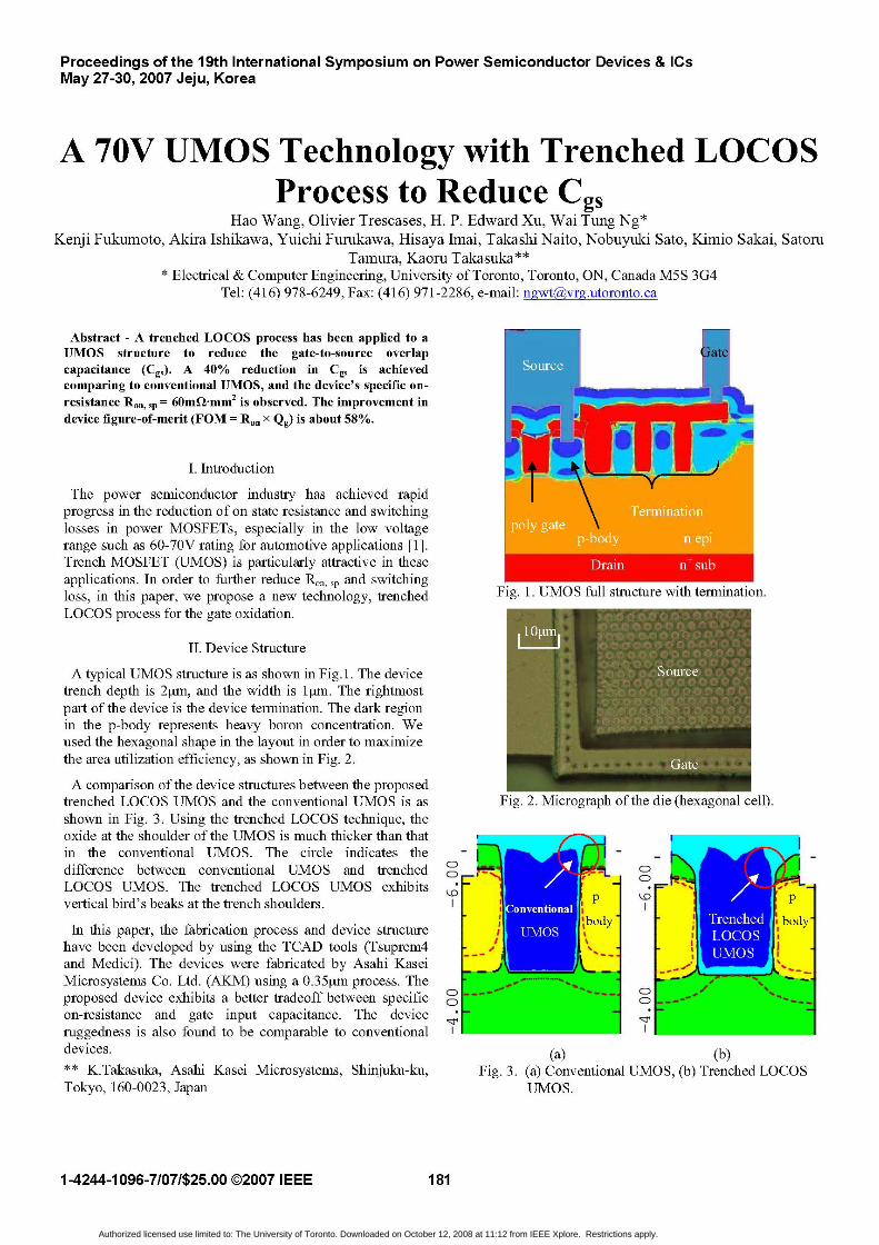
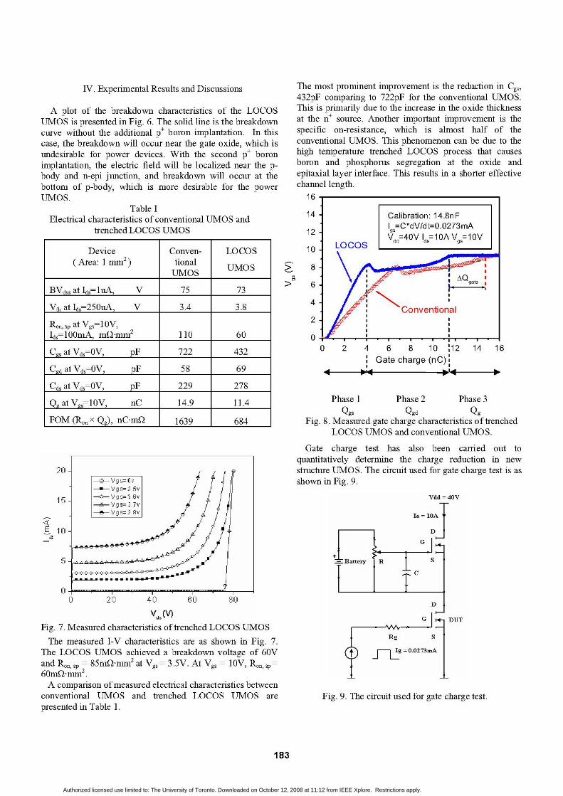
A typical UMOS structure is as shown in Fig.1. The devicetrench depth is 2pm, and the width is 1pm. The rightmostpart of the device is the device termination. The dark regionin the p-body represents heavy boron concentration. Weused the hexagonal shape in the layout in order to maximizethe area utilization efficiency, as shown in Fig. 2.
A comparison of the device structures between the proposedtrenched LOCOS UMOS and the conventional UMOS is as Fig. 2. Micrograph of the die (hexagonal cell).shown in Fig. 3. Using the trenched LOCOS technique, theoxide at the shoulder of the UMOS is much thicker than thatin the conventional UMOS. The circle indicates the -difference between conventional UMOS and trenchied c: C
LOCOS UMOS. The trenched LOCOS UMOS exhibitsvertical bird's beaks at the trench shoulders. P P
Dbody * bodyIn this paper, the fabrication process and device structure * *have been developed by using the TCAD tools (Tsuprem4and Medici). The devices were fabricated by Asahi Kasei -Microsystems Co. Ltd. (AKM) using a 0.35ptm process. Theproposed device exhibits a better tradeoff between specific clon-resistance and gate input capacitance. The deviceruggedness is also found to be comparable to conventional 71devices. (a) (b)** K.Takasuka, Asahi Kasei Microsystems, Shinjuku-ku, Fig. 3. (a) Conventional UMOS, (b) Trenched LOCOSTokyo, 160-0023, Japan UMOS.
1-4244-1096-7/07/$25.00 ©2007 IEEE 181
Authorized licensed use limited to: The University of Toronto. Downloaded on October 12, 2008 at 11:12 from IEEE Xplore. Restrictions apply.

III. Fabrication Process and Results
The device fabrication is based on a 7 ptm n-type epitaxiallayer with phosphorus doping of 5x 10i5 cm-3 on top of a
heavily As-doped n+ <110> substrate [2]. Boron and arsenicimplantation of 3x1013 cm-2 at 120keV and 3x10'5 cm-2 at1 00keV were used to produce the p-well and n+ source,
respectively.
Thereafter, a 2pim deep and [tm wide U-shaped trench was
dry etched and the trenched LOCOS process was carried outto form a thick oxide layer at the trench sidewall. The Si3N4deposition and etch back leaves open area to form LOCOS attrench bottom, and at trench shoulders (see Fig. 4). Thisprocess is simpler and easier to control when compared to theapproach of oxide deposition and etch back introduced byTakaya et al. [3].
Si3N4 deposition Dry etch LOCOS
After nitride removal and a brief sidewall oxide cleaning,gate oxidation at 9500C was performed to form a 600 A gateoxide on the trench wall. As visualized in simulation, thisrelatively high temperature oxidation causes some
segregation of boron and phosphorus at the oxide andepitaxial layer interface, which reduces the effective channellength, this also helps to reduce the device Ron, sp. On theother hand, the sidewall gate oxide thickness is increased atthe top part of the UMOS due to the trenched LOCOSprocess. This thick oxide at the n+ source decreases Cgs
significantly.In order to pinpoint the breakdown location to be at the
center of the p-body/n-epi junction, a second high energy
boron ion implantation through the body contact hole iscarried out.
Finally, a deep body source contact [4] was formed byshallow trenched Si etch and p+ boron implantation, becausedeep body source contact can greatly reduce the contactresistance, as indicated in Fig. 5.
(a)
Fig. 5. Schematic of p+ (2) boron implantationand deep body source contact formation.
io-2
103
104
-4_10
10o-
10-6
(b)Fig. 4. (a) Schematic of the trenched LOCOS process to form
thick oxide layers at trench bottom and shoulders. (b)A SEM cross sectional view of the UMOS structuresfabricated by conventional and trenched LOCOSprocess. Segregation reduces the effective channellength.
10-8
10-90 20 40 60 80
Vds (V)Fig. 6. Measured breakdown I-V curve of trenched
LOCOS UMOS with and without p+ (2) boronimplantation.
182
w/o 2nd boronimplantation
--- with 2nd boronimplantation
__:
Authorized licensed use limited to: The University of Toronto. Downloaded on October 12, 2008 at 11:12 from IEEE Xplore. Restrictions apply.
IV. Experimental Results and Discussions
A plot of the breakdown characteristics of the LOCOSUMOS is presented in Fig. 6. The solid line is the breakdowncurve without the additional p+ boron implantation. In thiscase, the breakdown will occur near the gate oxide, which isundesirable for power devices. With the second p+ boronimplantation, the electric field will be localized near the p-body and n-epi junction, and breakdown will occur at thebottom of p-body, which is more desirable for the powerUMOS.
Table IElectrical characteristics of conventional UMOS and
trenched LOCOS UMOS
Device Conven- LOCOS(Area: 1 mm2) tional UMOS
BVdss at Ids= luA, V 75 73
Vth at Ids=250uA, V 3.4 3.8
Ron sp at Vgs= V,Ids=l00mA, mQ mm2 110 60
Cgs at VdS=OV, pF 722 432
Cgd at Vds=OV, pF 58 69
Cds at Vds=OV, pF 229 278
Qg at Vgs= I OV, nC 14.9 1 1.4
FOM (Ron x Qg), nC mQ 1639 684
15
H 10
The most prominent improvement is the reduction in Cgs,432pF comparing to 722pF for the conventional UMOS.This is primarily due to the increase in the oxide thicknessat the n+ source. Another important improvement is thespecific on-resistance, which is almost half of theconventional UMOS. This phenomenon can be due to thehigh temperature trenched LOCOS process that causesboron and phosphorus segregation at the oxide andepitaxial layer interface. This results in a shorter effectivechannel length.
16
14 - Calibration: 14.8nF=C*dV/dt=0.0273mA
12- gsVdd=40V 10AV =10V
10 LOCOS
8-Un
6 -
4 -
2 -
rl _u0 2 4 6 8 10 :12
Gate charge (nC):14 16
Phase Phase 2 Phase 3Qgs Qgd Qg
Fig. 8. Measured gate charge characteristics of trenchedLOCOS UMOS and conventional UMOS.
Gate charge test has also been carried out toquantitatively determine the charge reduction in new
structure UMOS. The circuit used for gate charge test is as
shown in Fig. 9.
Vdd = 40V
0 20 40 60 80
Vds(V)Fig. 7. Measured characteristics of trenched LOCOS UMOS
The measured I-V characteristics are as shown in Fig. 7.The LOCOS UMOS achieved a breakdown voltage of 60Vand Ron s 85mQmm2 at Vgs = 3.5V. At Vgs = OV, Ron sp
60mQmm2.A comparison of measured electrical characteristics between
conventional UMOS and trenched LOCOS UMOS are
presented in Table 1.
DIJT
Fig. 9. The circuit used for gate charge test.
183
AQQ gate ,
>,......
IN _ IN__
Authorized licensed use limited to: The University of Toronto. Downloaded on October 12, 2008 at 11:12 from IEEE Xplore. Restrictions apply.

120
The upper power MOSFET is used as a current regulator toset the drain current. The gate source (Vgs) is 1OV, and the Vddis set to be 40V. Phase 1 in Fig. 8 represents a linear increasein Vgs with gate charge. Qgs defines the charge needed duringturn on. In phase 2, Vgs remains relatively constant, and thedrive current starts to charge the Miller capacitance, Cgd.During phase 3, the gate capacitance is the summation of Cgsand Cgd, and the total charge is Qg= Qgs+ Qgd, which isrequired to charge gate to Vgs = 10V.
Under this condition, the Qgs is 23% less for trenchedLOCOS UMOS. Overall, the FOM (Ron x Qg) has beenimproved by 58% without compromising the breakdownvoltage.
FOMConventional -FOMLOCOS 163 9-684 58°FOMconventional 1639
High speed switching, would induce a lot of stress on thedevice, which might lead to device damage. This occursespecially when switching with an inductive load. The rapidturn off of an inductive load can cause avalanche breakdownof the drain to source diode, resulting from Vds transients. [5]In order to determine the ruggedness of the new device, theUnclamped Inductive Switch (UIS) test was carried out forthe trenched LOCOS UMOS.
L 1.09n-LL
Vin I
Rg
Fig. 10. The circuit used for UIS test.
When the gate voltage is switched off, there is still aninductor current flowing through the circuit as maintained bythe collapsing inductive field. This current forces the internaldiode of the MOSFET into avalanche breakdown. If thecurrent is too large for the device to handle, the device will bepermanently destroyed. The inductor used for UIS test in Fig.10 is 1.09mH. From the UIS test results (Fig. 11), thetrenched LOCOS UMOS process demonstrates comparableruggedness as conventional UMOS. This is because theoverall process does not involve any doping change within thep-body or n-epi junction. The parasitic BJT inherent in theUMOS remains same.
12
10
8
4
2
00 100 200 300
Time (VtSec)
100
80
400 500
Fig. 11. UIS test results ofUMOS devices fabricated byconventional and trenched LOCOS process.
V. Conclusions
A novel trenched LOCOS UMOS technique has beenproposed and experimentally verified. This technique iseasy to carry out and the new device exhibits 40% reductionin Cgs, 58% improvement in FOM when compared toconventional device. The new device illustrates comparableruggedness as the conventional devices withoutcompromising the breakdown voltage.
Acknowledgements
The authors would like to thank AKM for financial supportand devices fabrication. We also want to thank Auto21,NSERC for financial support, and express our sinceregratitude to Jaro Pristupa for his continuous help with thesoftware tools.
Reference[1] F.G. Kassakian, D.J.Perreault, The future of electronics
in automobiles, proceedings ISPSD 2001, June 2001,Osaka, pp. 15-19.
[2] E. S. Ammar and T. J. Rogers, "UMOS Transistors on(110) Silicon," IEEE Trans. on Electron Devices, vol.ED-27, no. 5, pp. 907-914, 1980.
[3] H. Takaya, K. Miyaki, and A. Kurayanagi, et. al.,"Floating Island and Thick Bottom Oxide Trench GateMOSFET (FITMOS) - A 60V Ultralow On-resistanceNovel MOSFET with Superior Internal Body Diode",Proc. ISPSD, pp.1-5, 2005.
[4] S. S. Kim, J. K. Oh and M. K. Han, "A New TrenchedSource Power MOSFET Improving Avalanche Energy"Jpn. J. Appl. Phys., Vol. 42, pp. 2156-2158, 2003.
[5] J.P. Phipps and K. Gauen, "New Insights Affect PowerMOSFET Ruggedness", Conference Proceeding ofApplied Power Electronics Conference and Exposition,pp. 290-298, Feb, 1988.
184
14
Authorized licensed use limited to: The University of Toronto. Downloaded on October 12, 2008 at 11:12 from IEEE Xplore. Restrictions apply.


![GURSR ZHU GDPVD QGS ODQWV (QJLQHHULQJ … · ,0,$ :*3 &rqvwuxfwlrq dqgrs hudwlrqr i k\gursr zhu gdpvd qgs odqwv (qjlqhhulqj ,qvxudqfh ([srvxuh %\ $uplq $pvwxw] 6zlvv 1dwlrqdo ,qvxudqfh](https://img.dokumen.tips/doc/110x75/5b1d340b7f8b9add7f8b779d/gursr-zhu-gdpvd-qgs-odqwv-qjlqhhulqj-0-3-rqvwuxfwlrq-dqgrs-hudwlrqr-i.jpg)


![QGD)LW]SDWULFN %URZQ 0UV&KULVWLQH6KHUZRRG](https://img.dokumen.tips/doc/110x75/617c40c133744e76fe3229f6/qgdlwsdwulfn-urzq-0uvampkulvwlqh6khuzrrg.jpg)