Embed Size (px)
Citation preview

Technology Roadmap for Nanoelectronics(Ist200011)★from: ITRI-ITIS-MEMS-: [email protected]
Technology Roadmap for Nanoelectronics(Ist200011) ★
Index Technology Roadmap for Nanoelectronics(Ist200011)★____________________________1
Index-------------------------------------------------------------------------------------------------------------1About------------------------------------------------------------------------------------------------------------3Foreword-------------------------------------------------------------------------------------------------------4
1. Introduction______________________________________________________________6I.I. Markets.................................................................................................................................6
Figure 1: The Contribution of Electronics to the Gross Product 6Figure 2: Electronic Market Forecast 6
1.2. Applications..........................................................................................................................7Figure 3: Minimum Feature Size versus Year of Introduction. 8Table 1: Selected data from ITRS 1999 9Table 2: Technical Requirements for Memory Applications 11Figure 4: the System-on-a-Chip of the Future? 12Table 3: Technical Requirements fir Logic Applications 13
1.3. Public Investments in Nanotechnologies............................................................................14Table 4: Estimated Governmental Support to Nanoscience and Technology in Europe 15Figure 5: Nature of the NID Projects 17
2. Reference Point: MOSFETS________________________________________________192.1. Theoretical Limits..............................................................................................................19
Figure 6: Energy -- Delay Diagram for Electronics 192.2. Technology limits...............................................................................................................192.3. Economical Limits..............................................................................................................20
Figure 7: Cost of a Semiconductor Facility. 202.4. Major Challenges and Difficulties.....................................................................................20
3. Emerging Devices_________________________________________________________223.1. Single Electron Tunnelling Devices...................................................................................22
3.1.1. Single Electron Transistors-----------------------------------------------------------------------22Figure 8: Principle of a Single Electron Transistor 22
3.1.2. Nano-flash device-----------------------------------------------------------------------------------243.1.3. Yano memory----------------------------------------------------------------------------------------243.1.4. Device Parameters and future challenges-----------------------------------------------------24
Table 5: Comparison between Conventional and Single Electron Memories. 253.2. Tunnelling Diodes..............................................................................................................26
Figure 9: Concept of an Interband Tunnelling Diode 26Figure 10: An Interband Tunnelling Device in Operation 27
3.2.2. Resonant Tunnelling Diode-----------------------------------------------------------------------27Figure II: Concept ofa Resonant Tunnelling Device. 27
3.2.3. Tunnel Diodes Performance----------------------------------------------------------------------27Figure 12: Oscillation Frequencies for ITD and RTD. 28Table 6: Comparison of Tunnelling Devices Parameters 28
3.2.4. Concepts for Three Terminal Resonant Tunnelling devices------------------------------28Figure 13: Concepts for three terminal tunnelling devices 29
3.2.5. Major Challenges and Difficulties for TDs----------------------------------------------------303.3. Rapid Single Flux Quantum Logi......................................................................................30
3.3.1. Principle of Operation-----------------------------------------------------------------------------303.3.2. Technology, Critical Dimensions and Performance----------------------------------------313.3.3. Major Challenges and Difficulties for RSFQ-------------------------------------------------32
3.4. Molecular Nanoelectronics.................................................................................................323.4.1. Electric-field based molecular switching devices--------------------------------------------33
Figure 14: Transport through a Molecule 33【/tt/file_convert/5aad6b677f8b9a2b4c8e78e4/document.doc】
All: 107 pages(2023/5/6)【1 】
Technology Roadmap for Nanoelectronics(Ist200011)★from: ITRI-ITIS-MEMS-: [email protected]
3.4.2. Alternative molecular components--------------------------------------------------------------343.4.3. Molecular modelling--------------------------------------------------------------------------------35
Figure 15: Scheme of a Hybrid Metal-Molecule-Semiconductor Structure. 353.4.4. Major challenges and difficulties for molecular electronics-------------------------------36
3.5. Spin Devices........................................................................................................................363.5.1. Spin Valve Devices----------------------------------------------------------------------------------37
Figure 16: Scheme of a Spin Valve 373.5.2. Tunnel Junction Devices--------------------------------------------------------------------------38
Figure 17: Scheme of a Tunnel function 383.5.3. Spin injection devices------------------------------------------------------------------------------383.5,4. Performance------------------------------------------------------------------------------------------393.5.5. Challenges and Difficulties------------------------------------------------------------------------40
3.6. Wave interference devices: Electronic Waveguiding and Quantum Interference Devices403.6.1. The basics of Coherent Switching and Interference----------------------------------------413.6.2, Technology and Critical Dimensions-----------------------------------------------------------423.6.3. Quantum Point Contacts and electronic waveguides---------------------------------------423.6.4. Double electron waveguide device---------------------------------------------------------------433.6.5. The 3-terminal (Y-Branch) switching devices------------------------------------------------43
Figure 18: Y-branch Switch 443.6:6. Major challenges and difficulties for electron interference and switching devices- -45
4. Nanofabrication__________________________________________________________46Table 7: Maturity of Lithography Options 46Table 8: Practical and Ultimate Resolution Limits for Lithography 46
4.1. Lithography for CMOS technology...................................................................................484.1.1. Optical lithography---------------------------------------------------------------------------------484.1.2. Extreme Ultraviolet lithography-----------------------------------------------------------------484.1.3. X-ray proximity lithography---------------------------------------------------------------------494.1.4. E-beam projection lithography and Scalpel--------------------------------------------------494.1.5. Ion beam projection--------------------------------------------------------------------------------51
Table 9: Sensitivity perType of Lithography 514.2. Emerging nanofabrication methods...................................................................................52
4.2.1.Electron Beam Nanolithography-----------------------------------------------------------------52Table 10: Resolution and Sensitivity for E-beam Lithography 52
4.2.3.1. Imprint 53Figure 19: The Imprint Process 53
4.2.3.2 Inking 55Figure 20: The Inking Process 55
4.2.3.3. Comparison of printing techniques and applications 56Table II: Comparison of Printing Techniques 56
4.2.4. Bottom Up Approaches----------------------------------------------------------------------------574.3. Comparison of Fabrication Techniques............................................................................58
Figure 21: Throughput us resolution for Different Exposure Techniques 58
5, Circuits and Systems______________________________________________________605.1. Design Strategies: Interconnect Problems and Design Complexity..................................60
Figure 22: Design Hierarchies for Nanoscale Circuits 61Figure 23: CMOS Gate Delay vs Gate Length 61
5.1.1. Impact of Increasing Clocking Frequencies on Nanoscale Circuits---------------------615.1.2. Local Architectures---------------------------------------------------------------------------------62
5.2. Novel Circuitly....................................................................................................................635.2.1. Resonant Tunnelling Device Circuits----------------------------------------------------------63
Figure 24: RTD/HFET Circuits 64Table 12: Performance for Tunnelling Based SRAM and Si Memory 64
5.2.2. QCA circuits-----------------------------------------------------------------------------------------65Figure 25: The Two Polarization States in a QCA Cell 66
【/tt/file_convert/5aad6b677f8b9a2b4c8e78e4/document.doc】All: 107 pages(2023/5/6)【2 】
Technology Roadmap for Nanoelectronics(Ist200011)★from: ITRI-ITIS-MEMS-: [email protected]
Figure 26: Logic Functions Based upon a QCA Majority Voting Gate 66Figure 27: Dot Distance Requirements for a QCA Circuit 66
5.3. Current Trends in Novel System Architectures................................................................685.3.1. Starting Point: Systems on chip and Innovations in Microprocessor Designs--------68
Figure 28: Intelligent RAM Chip (IRAM) 685.3.2. Parallel Processing----------------------------------------------------------------------------------68
5.3.2.1. Propagated Instruction Processor 69Figure 29: Propagated Instruction Processor 69
5.3.2.2. Reconfigurable Hardware: From Reconfigurable Microprocessor Arrays to Defect Tolerant Circuits 69
Figure 30: The Reconfigurable Architechture Workstation (RAW) 705.3.3. DNA Computing■----------------------------------------------------------------------------------715.3.4. Artificial Neural Networks------------------------------------------------------------------------715.3.5. Quantum Information Processing (QIP)------------------------------------------------------72
5.4. Comparison of the Various System Architectures.............................................................74Figure 32: Aspects of Architectures for Nanoelectronic Systems 75Table 13: Components of Nanoelectronic Architectures 75Figure 33: Comparison of Architectures 76
6. Conclusions______________________________________________________________776.1. Devices................................................................................................................................776.2. Fabrication.........................................................................................................................786.3. Architectures......................................................................................................................796.4. Outlook...............................................................................................................................79
7. Comparison Between Technologies__________________________________________807.1. Notes:..................................................................................................................................807.2. Comparative Tables between alternatives for memory and logic applications................81
Table 14: Comparison Memory Devices Year 2000 81Table 15: Forecast Memory Devices Year 2006 82Table 16: Forecast Memory Devices Year 2012 82Table 17: Comparison Logic I High Frequency Devices Year 2000 (in production) 83Table 18: Comparison Logic I High Frequency Devices Yar 2000 (in research) 83Table 19: Forecast Logic I High Frequency Devices Yar 2006 84Table 20: Forecast Logic I High Frequency Devices Year 2012 84Table 21: Comparison Circuit Performance Year 2000 85Table 22: Forecast Circuit Performance Year 2006 85Table 23: Forecast Circuit Performance Year 2012 86
8. Annex__________________________________________________________________878.1. Glossary..............................................................................................................................878.2. Research Projects...............................................................................................................878.3. Contributors.......................................................................................................................888.4. References............................................................................................................................89
About Rarnon CompanoEuropean CommissionDirectorate-General Information SocietyRue de la Loi
2000B-1049 Brusselse-mail: [email protected]
Neither the European Commission nor any person acting on behalf of the Commissionis responsible for the use which might be made of the following information
Atomic Force Microscopy (AFM) image of a modified silicon surface. Thetext was written by locally oxidising the silicon surface with an AFM tip. Eachletter is 80 nm in size consisting of a series of individual dots with a diameter of 20 nm.M. Calleja, F. Garcia and R. Garcia (CSIC -
【/tt/file_convert/5aad6b677f8b9a2b4c8e78e4/document.doc】All: 107 pages(2023/5/6)【3 】
Technology Roadmap for Nanoelectronics(Ist200011)★from: ITRI-ITIS-MEMS-: [email protected]
CNN Madrid)
Design and layout of the brochure from the INFSO DG/R6 - Information & Communications Unit
A great deal of additional information on the European Union is available on the Internet.It can be accessed through the Europa server (http://europa.eu.int).Cataloguing data can be found at the end of this publication.Luxembourg: Office for Official Publications of the European Communities, 2001ISBN 92-894-0170-2@ European Communities, 2001Reproduction is authorised provided the source is acknowledged.Printed in BelgiumPRINTED ON WHITE CHLORINE-FREE PAPER
Foreword The IT revolution is based on an "exponential" rate of technological progress. For example,
internet traffic doubles every 6 months, wireless capacity doubles every 9, optical capacity doubles every 12, magnetic information storage doubles every 15, etc. The most famous example is "Moore's law" which indicates that the performance of semiconductor devices doubles every 18 months. Moore's observation has been valid for three decades and has been a fundamental tool for business planning in the semiconductor industry. Fundamental laws of physics limit the shrinkage of CMOS on which Moore's Law is based, at least on current approaches. Even before these physical limits are reached there are strong indications that severe engineering pro- blems, as well as the need for huge investment, may slow down the growth in inte- grated circuit performance. The continuation of the IT revolution is predicated on new ideas for information storage or processing, leading to future applications. One option is to look for mechanisms that operate at the nanoscale and exploit quantum effects. The objective of this document is to monitor device concepts currently under investigation, to discuss the feasibility of their large scale integration and of ways to fabricate them. Giving a description of the state of the art in a field is an exercise which is commonly undertaken with success; extrapolating into the future is not so obvious. Making predictions in an emergent field is even more difficult. By its nature, no forecast can reflect all the views of all the experts in the field; it can try, at best, to reflect a con- sensus of most of their views. In order to arrive at a "common view", the editor has collected information from many sources. In particular, he has relied greatly upon the discussions of the six monthly MELARI/NID workshops whose participants are drawn from more than sixty distinct Europe research groups working in differentareas of nanoelectronics.The first technology roadmap for nanoelectronics was published by L. Molenkamp,D. Paul and R. Compano in April 1999 and this new edition follows the same for-mat. This new edition has been expanded by new chapters reflecting new tendencies.In particular, P. Lindelof and L. Samuelson have provided the information forChapter 3.6 on wave interference devices, C. Sotomayor for Chapter 4.2.3 on prin-ting techniques, Ch. Pacha and W. Prost for Chapter 3.2.1 on interband tunnellingdevices and M. Macucci for Chapter 3.4.3 on molecular approaches. In addition,many persons have contributed by updating the chapters on Emerging Devices, onNanofabrication and Circuits &: Architectures and the tables on the performanceforecast. They are mentioned in the back of this document. R. Compano has beenin charge of balancing the different views and summarising the conclusions.Many top nanotechnology experts contributed to this document, but predictions cannever be guaranteed. This roadmap should be understood as a document that mo-nitors progress and discusses tendencies in the hope that it may help the reader toappreciate strengths, weaknesses, threats and opportunities of different technologies.Although breakthroughs are not usually predicted, they very often occur as unex-pected results when working towards predicted targets,Simon Bensasson Head of Unit "Future and Emerging Technologies"
【/tt/file_convert/5aad6b677f8b9a2b4c8e78e4/document.doc】All: 107 pages(2023/5/6)【4 】

Technology Roadmap for Nanoelectronics(Ist200011)★from: ITRI-ITIS-MEMS-: [email protected]
【/tt/file_convert/5aad6b677f8b9a2b4c8e78e4/document.doc】All: 107 pages(2023/5/6)【5 】
Technology Roadmap for Nanoelectronics(Ist200011)★from: ITRI-ITIS-MEMS-: [email protected]
1. Introduction
A "roadmap" is an extended look at the future composed from the collective knowledge of experts in thefield. A roadmap encompasses trends in the area, links and comparisons between different fields, identifi-cation of discontinuities or knowledge voids and highlights potential major show-stoppers. Before ente-ring into the nanoelectronics world, first the tendencies and limits of "classical CMOS" technology will bereviewed. Alternative nanoelectronic options will then be positioned from the point of view of potentialmarkets, technological progress and scientific challenges.
I.I. Markets 100000 -
10000
1000
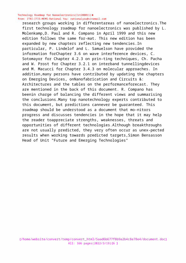
Figure 1: The Contribution of Electronics to the Gross Product
The evolution of the semiconductor products turnover and the world electronics sales is shownwith respect to the gross world, product. The lines indicate the hypothetical assumption that thegrowth rate will be maintained in the next two decades. Reworked from Ref. 243
Figure I shows the evolution of the world electronics sales compared to the gross product of the wholeworld. The former increases substantially quicker than the latter, indicating that information technologiesare one of the major drivers of the world-wide economy. Within the electronics business, semiconductorproducts have a dominant role and their turnover grows at a higher rate than the overall electronics mar-ket. Within the semiconductor sector, memories (DRAM), processors (MPU), application specific inte-grated circuits (ASIC) and digital signal processors (DSP) are the most prominent products. What aboutthe future? Simplest would be to extrapolate the existing data. But take care, this approach is dangerousand may lead to wrong
【/tt/file_convert/5aad6b677f8b9a2b4c8e78e4/document.doc】All: 107 pages(2023/5/6)【6 】
Technology Roadmap for Nanoelectronics(Ist200011)★from: ITRI-ITIS-MEMS-: [email protected]
interpretations. For example, a linear extrapolation of the points in Figure I wouldmake the lines cross at a certain point in time. This would mean that the gross world product is smallerthan the electronics sales, and the latter smaller than the semiconductor sales, which is a clear contradic-tion. To predict the market volume therefore only makes sense for a reasonable time frame.
Figure 2: Electronic Market Forecast
Turnover for all electronic products, its semiconductor segment and the equipment for the pro-duction of semiconductor products (in Bf@.) [Ref. 243]A forecast shorter in time, but more accurate, is given in Figure◆ 2, It compares the turnover of electronicsproducts, its segment of semiconductor chips and the sub-segment of equipment for the production ofsemiconductor products for the years 1999 and 2004. The latter date is interesting from the nanotechno-logy point of view, as the semiconductor industry associations assume that they will be close to introdu-cing 100 nm groundrule technology [Ref. 104]. As will be explained later sub 100 nm is a kind of "tur-ning point", where many radically new technologies will have to be developed, some of them paving theway for real nanofabrication. From the nanofabrication point of view a comparison of the 1999 and 2004data is interesting because:@ The overall electronics sales will exhibit a notable increase by 53% (from 935 @ to 1433 B@) and semi-conductor products will rise even more (117%, from 296 Beuro to 136 B@S). Let's assume very conserva-tively that most semiconductor products will still be CMOS based, for instance 93% - 95%. The absolutevalue of the remainder non-CMOS 5%-7% share is huge and attractive for innovative circuit concepts,including nanotechnology based ones.@ The impressive increase for chip manufacturing equipment of 147% (from 26.5 B@ to 65.5 B@) mayhave a very positive effect on nanotechnology. As CMOS devices will reach sub 100 nm feature sizes, non-optical exposure tools may be employed whose operating principle works also at smaller scales. For exam-ple, printing technologies that may be employed for manufacturing 100 nm CMOS devices and could alsobe employed for nanofabrication down to 10 nm.Although CMOS products may still dominate the electronics market, other smaller volume applicationsare worthwhile discussing as they presntly exhibit a large growth rate and have a potential for futuregrowth. Moreover, they may serve as an example for a successful introduction of a new family of products.Here a short, not exclusive, overview:@ In a few years from now, magnetoelectronics may achieve sales in the order of 135 B@. Magneto-sensorsand magnetic hard discs have already now an established market of 3 B@ and 40 B@, respectively. Othermagnetoelectronic products, that in 1999 had a market of I B@ [Ref. 18] will enter into new markets, name-ly MRAM (35 B@) substituting part of the DRAM, SRAM and EPROMs business, Spintransistors (50 Be)entering the markets
【/tt/file_convert/5aad6b677f8b9a2b4c8e78e4/document.doc】All: 107 pages(2023/5/6)【7 】

Technology Roadmap for Nanoelectronics(Ist200011)★from: ITRI-ITIS-MEMS-: [email protected]
of logic circuits, spin-optoelectronics (6 B@) replacing part ofoptoelectonics, magne-tocouplers (I B@) for optocouplers and MRAM-bio-chips (0.25 B@) for classical biochips [Ref. 143].@ Optoelectronics systems understood as optocouplers, components for optical transmission, optical harddisks and laser components had a world market of 1.5 B@ in 1999. It is expected that this value will
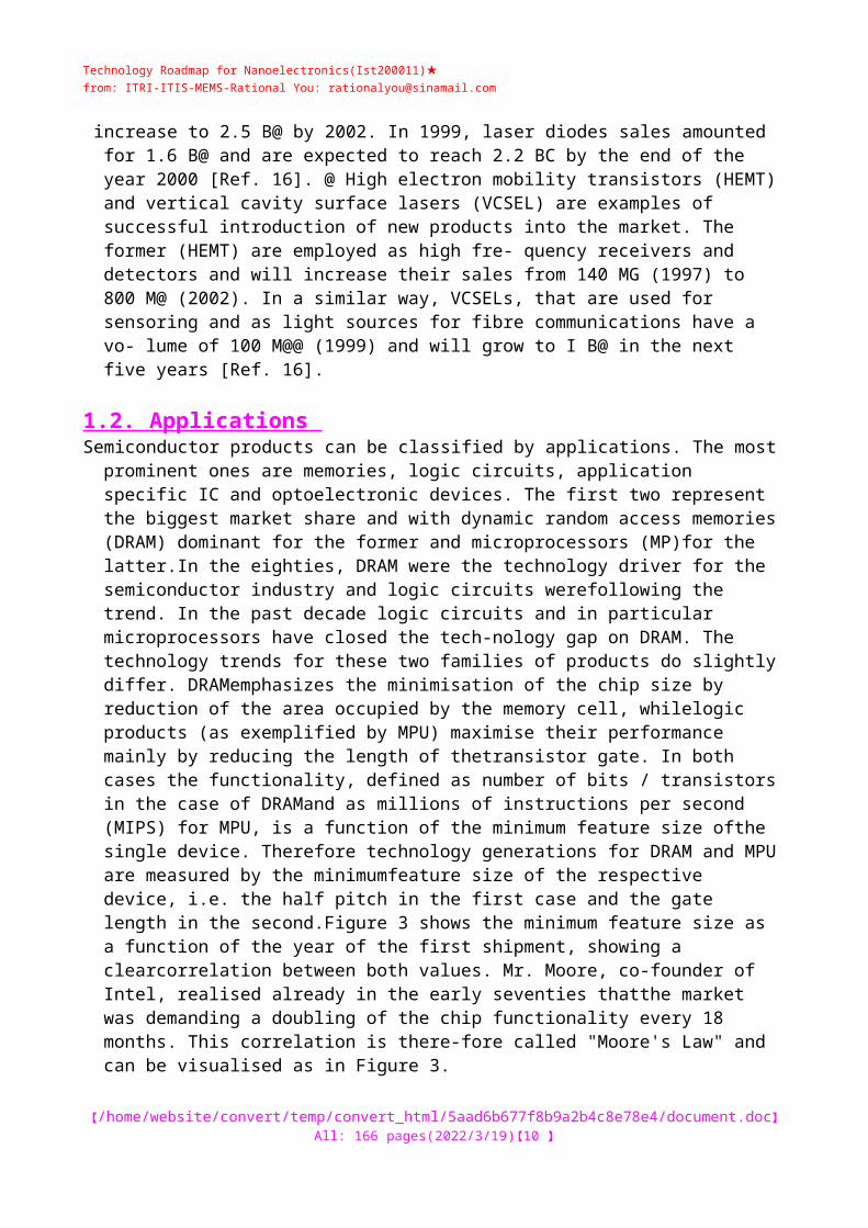
increase to 2.5 B@ by 2002. In 1999, laser diodes sales amounted for 1.6 B@ and are expected to reach 2.2 BC by the end of the year 2000 [Ref. 16]. @ High electron mobility transistors (HEMT) and vertical cavity surface lasers (VCSEL) are examples of successful introduction of new products into the market. The former (HEMT) are employed as high fre- quency receivers and detectors and will increase their sales from 140 MG (1997) to 800 M@ (2002). In a similar way, VCSELs, that are used for sensoring and as light sources for fibre communications have a vo- lume of 100 M@@ (1999) and will grow to I B@ in the next five years [Ref. 16].
1.2. Applications Semiconductor products can be classified by applications. The most prominent ones are memories,
logic circuits, application specific IC and optoelectronic devices. The first two represent the biggest market share and with dynamic random access memories (DRAM) dominant for the former and microprocessors (MP)for the latter.In the eighties, DRAM were the technology driver for the semiconductor industry and logic circuits werefollowing the trend. In the past decade logic circuits and in particular microprocessors have closed the tech-nology gap on DRAM. The technology trends for these two families of products do slightly differ. DRAMemphasizes the minimisation of the chip size by reduction of the area occupied by the memory cell, whilelogic products (as exemplified by MPU) maximise their performance mainly by reducing the length of thetransistor gate. In both cases the functionality, defined as number of bits / transistors in the case of DRAMand as millions of instructions per second (MIPS) for MPU, is a function of the minimum feature size ofthe single device. Therefore technology generations for DRAM and MPU are measured by the minimumfeature size of the respective device, i.e. the half pitch in the first case and the gate length in the second.Figure 3 shows the minimum feature size as a function of the year of the first shipment, showing a clearcorrelation between both values. Mr. Moore, co-founder of Intel, realised already in the early seventies thatthe market was demanding a doubling of the chip functionality every 18 months. This correlation is there-fore called "Moore's Law" and can be visualised as in Figure 3.
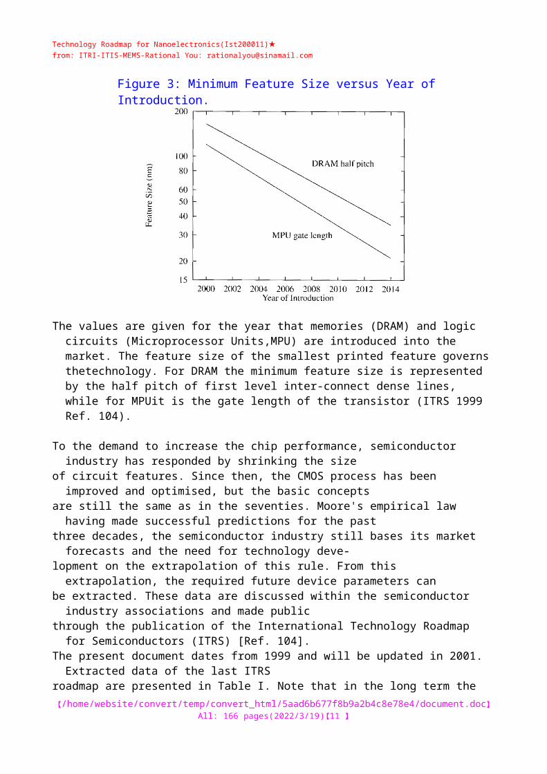
Figure 3: Minimum Feature Size versus Year of Introduction.
【/tt/file_convert/5aad6b677f8b9a2b4c8e78e4/document.doc】All: 107 pages(2023/5/6)【8 】

Technology Roadmap for Nanoelectronics(Ist200011)★from: ITRI-ITIS-MEMS-: [email protected]
The values are given for the year that memories (DRAM) and logic circuits (Microprocessor Units,MPU) are introduced into the market. The feature size of the smallest printed feature governs thetechnology. For DRAM the minimum feature size is represented by the half pitch of first level inter-connect dense lines, while for MPUit is the gate length of the transistor (ITRS 1999 Ref. 104).
To the demand to increase the chip performance, semiconductor industry has responded by shrinking the size
of circuit features. Since then, the CMOS process has been improved and optimised, but the basic concepts
are still the same as in the seventies. Moore's empirical law having made successful predictions for the past
three decades, the semiconductor industry still bases its market forecasts and the need for technology deve-
lopment on the extrapolation of this rule. From this extrapolation, the required future device parameters can
be extracted. These data are discussed within the semiconductor industry associations and made public
through the publication of the International Technology Roadmap for Semiconductors (ITRS) [Ref. 104].
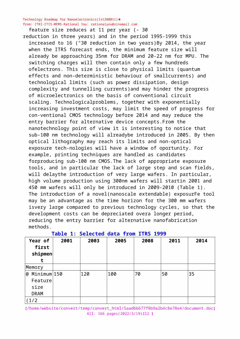
The present document dates from 1999 and will be updated in 2001. Extracted data of the last ITRSroadmap are presented in Table I. Note that in the long term the feature size reduces at 11 per year
(- 30reduction in three years) and in the period 1995-1999 this increased to 16 ("30 reduction in two
years)By 2014, the year when the ITRS forecast ends, the minimum feature size will already be approaching 35nm for DRAM and 20-22 nm for MPU. The switching charges will then contain only a few hundreds ofelectrons. This size is close to physical limits (quantum effects and non-deterministic behaviour of smallcurrents) and technological limits (such as power dissipation, design complexity and tunnelling currents)and may hinder the progress of microelectronics on the basis of conventional circuit scaling. Technologicalproblems, together with exponentially increasing investment costs, may limit the speed of progress for con-ventional CMOS technology before 2014 and may reduce the entry barrier for alternative device concepts.From the nanotechnology point of view it is interesting to notice that sub-100 nm technology will
【/tt/file_convert/5aad6b677f8b9a2b4c8e78e4/document.doc】All: 107 pages(2023/5/6)【9 】
Technology Roadmap for Nanoelectronics(Ist200011)★from: ITRI-ITIS-MEMS-: [email protected]
alreadybe introduced in 2005. By then optical lithography may reach its limits and non-optical exposure tech-nologies will have a window of oportunity. For example, printing techniques are handled as candidates forproducing sub-100 nm CMOS.The lack of appropriate exposure tools, and in particular the lack of large step and scan fields, will delaythe introduction of very large wafers. In particular, high volume production using 300nm wafers will startin 2001 and 450 mm wafers will only be introduced in 2009-2010 (Table 1). The introduction of a novel(nanoscale extendable) exposurFe tool may be an advantage as the time horizon for the 300 mm wafers isvery large compared to previous technology cycles, so that the development costs can be depreciated overa longer period, reducing the entry barrier for alternative nanofabrication methods.
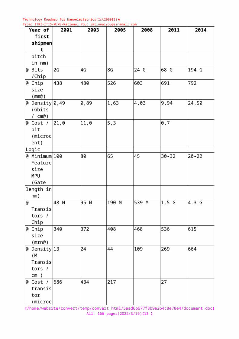
Table 1: Selected data from ITRS 1999Year of first
shipment2001 2003 2005 2008 2011 2014
Memory@ Minimum
Feature size DRAM
150 120 100 70 50 35
(1/2 pitch in nm)
@ Bits /Chip 2G 4G 8G 24 G 68 G 194 G@ Chip size
(mm@)438 480 526 603 691 792
@ Density (Gbits / cm@)
0,49 0,89 1,63 4,03 9,94 24,50
@ Cost / bit (microcent)
21,0 11,0 5,3 0,7
Logic@ Minimum
Feature size MPU (Gate
100 80 65 45 30-32 20-22
length in nm)@
Transistors / Chip
48 M 95 M 190 M 539 M 1.5 G 4.3 G
@ Chip size (mrn@)
340 372 408 468 536 615
@ Density (M Transistors / cm )
13 24 44 109 269 664
@ Cost / transistor (microcent)
686 434 217 27
【/tt/file_convert/5aad6b677f8b9a2b4c8e78e4/document.doc】All: 107 pages(2023/5/6)【10 】
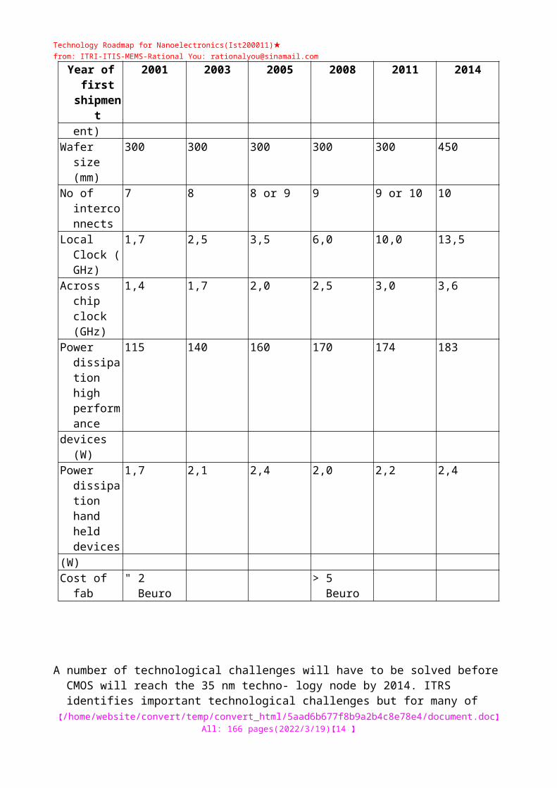
Technology Roadmap for Nanoelectronics(Ist200011)★from: ITRI-ITIS-MEMS-: [email protected]
Year of first shipment
2001 2003 2005 2008 2011 2014
Wafer size (mm)
300 300 300 300 300 450
No of interconnects
7 8 8 or 9 9 9 or 10 10
Local Clock ( GHz)
1,7 2,5 3,5 6,0 10,0 13,5
Across chip clock (GHz)
1,4 1,7 2,0 2,5 3,0 3,6
Power dissipation high performance
115 140 160 170 174 183
devices (W)Power
dissipation hand held devices
1,7 2,1 2,4 2,0 2,2 2,4
(W)Cost of fab " 2 Beuro > 5 Beuro
A number of technological challenges will have to be solved before CMOS will reach the 35 nm techno- logy node by 2014. ITRS identifies important technological challenges but for many of them no solutions are outlined. This lack of solutions may offer a window of opportunity for alternative devices. But assu- ming that semiconductors will keep track with the ITRS predictions, then (in 2014) an alternative tech- nology must perform better than CMOS on at least one of the following criteria in order to be competitive: @ Density: Over 6x10" transistors / cm@ (for logic) or over 2x10'@ bits per cm@ (for memory) @ Price: Cost of less than 27 m@ / transistor for logic, less than 660 ncent / bit for memory (data for 2011) ' Power Consumption: The equivalent of 1,4 billion transistors in a microprocessor must consume less than 183 W power. Alternatively, for hand held battery driven applications, these should consume less than 2.4 W @ Performance: operate at 13.4 GHz or offering an equivalent MIPS value (millions of instructions per second). The main drivers for research in microelectronics are computing, telecommunications, consumer electron- ics and military applications. The latter has a restricted volume but it is of strategic importance. Moreover, military research has often found its way in civil applications. In addition to these four areas, other appli- cations, such as electronics for research purposes, may play an inspirational role, but the markets for these applications are small. Space applications also belong to this last category, but they are interesting from the research point of view due to their extreme technical requirements. Up to now, progress in CMOS memory and logic has been driven by the need for ever faster personal and high performance computers as the complexity, power and volume of software and networking has increased. It is not evident how long this trend will continue. On one hand, personal computers
【/tt/file_convert/5aad6b677f8b9a2b4c8e78e4/document.doc】All: 107 pages(2023/5/6)【11 】
Technology Roadmap for Nanoelectronics(Ist200011)★from: ITRI-ITIS-MEMS-: [email protected]
already offer sufficiently good performance for a large number of users. On the other hand, new applications, suchas automatic voice recognition or PC wireless communications, may give new impulses for further ICprogress.Consumer electronics is rapidly developing. In recent years we have observed the appearance of new homeentertainment appliances requiring a lot of processing and memory power. Playstations are examples oflarge volume products that require very sophisticated semiconductor components. Moreover, many "clas-sical" applications offer better consumer satisfaction by the use of more sophisticated semiconductor pro-ducts. For example, the reduction in size and weight of video cameras puts great challenges on the per-formance and power consumption of the semiconductor components.Mobile phones are a significant driver for Si (and SiGe, GaAs) technology. The mobile phone penetrationin the European Union is high, but there is plenty of room before the saturation occurs. Moreover, mobiletelephones have a short lifetime before they are replaced by more sophisticated models, for example inclu-ding WAP, or they get simply lost. The setting up of the UTMS network will again call for new phones andbase stations, which will give new impulses to the semiconductor industry. The new telecommunicationsstandard requires high speed switching. Many solutions are mixed with optics by the fibre optic cable andhence III-V solutions may dominate. Portable products are driven by low power technology where batteryperformance is almost static and higher performance must be achieved in the microelectronics.System-on-a-chip approaches would allow cheaper phones with longer battery lifetimes and higher datatransfer rates. As both radio frequency and infrared technologies become cheaper, market share is climbingfor both technologies. Such technology may allow wireless computer networking where avoiding the clut-ter of cables around the office or home, especially with portable computers, suggests another market.System-on-a-chip integrates many different functional Si-based (and perhaps other) devices on one singleSi chip (Figure 4). By contrast. Multi-chip modules (MCMs) having 2 or 3 independent chips rather thanI chip could have advantages. For example, Intel realised that manufacturing both logic and memory inone single process, leads to a dropping in the fields of the Pentium processors, because the optimised pro-duction process of the former is not fully compatible with that of the latter and vice versa. Another pro-blem is cross-talk, especially when digital and analogue components are placed on the same chip. Moreover,it is easier to test smaller units; hence, 2 or 3 chip solutions in MCMs may be preferable to complete sys-tems-on-a-chip. The application will determine the final chip count.
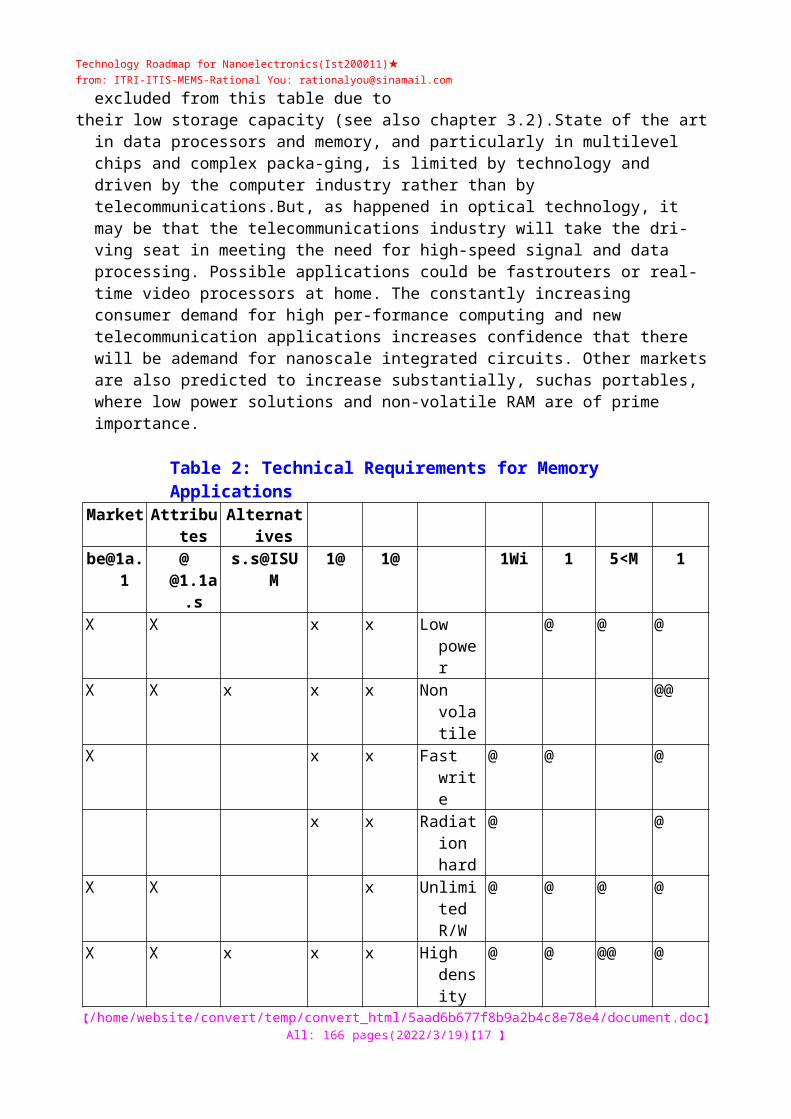
The X's indicate the set of requirements for different memory applications, while the @ s repre-sent the attributes of currently existing alternative technologies. @@ indicates the major strengthof analternative device compared to CMOS technology, i.e. static or dynamic RAM. AlthoughRTD memory circuits have been demonstrated, they have been excluded from this table due totheir low storage capacity (see also chapter 3.2).State of the art in data processors and memory, and
particularly in multilevel chips and complex packa-ging, is limited by technology and driven by the computer industry rather than by telecommunications.But, as happened in optical technology, it may be that the telecommunications industry will take the dri-ving seat in meeting the need for high-speed signal and data processing. Possible applications could be fastrouters or real-time video processors at home. The constantly increasing consumer demand for high per-formance computing and new telecommunication applications increases confidence that there will be ademand for nanoscale integrated circuits. Other markets are also predicted to increase substantially, suchas portables, where low power solutions and non-volatile RAM are of prime importance.
Table 2: Technical Requirements for Memory Applications【/tt/file_convert/5aad6b677f8b9a2b4c8e78e4/document.doc】
All: 107 pages(2023/5/6)【12 】
Technology Roadmap for Nanoelectronics(Ist200011)★from: ITRI-ITIS-MEMS-: [email protected]
Market Attributes
Alternatives
[email protected] @ @1.1a.
s
s.s@ISU M 1@ 1@ 1Wi 1 5<M 1
X X x x Low power
@ @ @
X X x x x Non volatile
@@
X x x Fast write @ @ @x x Radiation
hard@ @
X X x Unlimited R/W
@ @ @ @
X X x x x High density
@ @ @@ @
X X x x x Highly reliable
@ @ @
X X x x x Random access
@ @ @ @
X X x Fast access
@ @ @ @
X X x x x Fast read @ @ @X X x x x Low
write power
@ @ @
x Long term storage
@ @ @
X X x x x NoiseX X x x x Testing @ @ @
x High power
opticalwaveguides
opticaldetectors
spindevices
CMOS /BiCMOS
【/tt/file_convert/5aad6b677f8b9a2b4c8e78e4/document.doc】All: 107 pages(2023/5/6)【13 】
Technology Roadmap for Nanoelectronics(Ist200011)★from: ITRI-ITIS-MEMS-: [email protected]
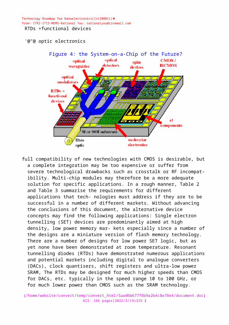
RTDs +functional devices
'@"@ optic electronics
Figure 4: the System-on-a-Chip of the Future?
full compatibility of new technologies with CMOS is desirable, but a complete integration may be too expensive or suffer from severe technological drawbacks such as crosstalk or RF incompat-ibility. Multi-chip modules may therefore be a more adequate solution for specific applications. In a rough manner, Table 2 and Table 3 summarise the requirements for different applications that tech- nologies must address if they are to be successful in a number of different markets. Without advancing the conclusions of this document, the alternative device concepts may find the following applications: Single electron tunnelling (SET) devices are predominantly aimed at high density, low power memory mar- kets especially since a number of the designs are a miniature version of flash memory technology. There are a number of designs for low power SET logic, but as yet none have been demonstrated at room temperature. Resonant tunnelling diodes (RTDs) have demonstrated numerous applications and potential markets including digital to analogue converters (DACs), clock quantisers, shift registers and ultra-low power SRAM, The RTDs may be designed for much higher speeds than CMOS for DACs, etc. typically in the speed range 10 to 100 GHz, or for much lower power than CMOS such as the SRAM technology. Rapid Single Flux Quantum (RSFQ) is a digital circuit technology which offers high speed in the GHzregime while producing low dissipation. As the super-conducting effects upon which the principle is basedwork already with feature sizes in the micrometer regime, RSFQ has the potential to enter the market forapplications where Si-CMOS cannot achieve the same frequencies. One major application is in high speedanalogue- to-digital and digital-to-analogue conversion. Unfortunately, RSFQ systems need cooling, aug-menting the overall costs of the whole system.Numerous magnetic memories have been demonstrated which are aimed at the non-volatile memory mar-ket such as that required in portable electronics. Because magnetism is an inherent property of the mate-rial in the memory, the devices have long retention times without requiring power to retain the memorystates. At present, access speeds are slow compared to DRAM but predictions show that similar speeds toDRAM are possible and the technology may ultimately be scaled to smaller dimensions and higher densi-ties than DRAM.
【/tt/file_convert/5aad6b677f8b9a2b4c8e78e4/document.doc】All: 107 pages(2023/5/6)【14 】

Technology Roadmap for Nanoelectronics(Ist200011)★from: ITRI-ITIS-MEMS-: [email protected]
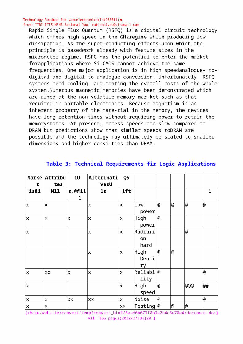
Table 3: Technical Requirements fir Logic Applications
Market Attributes
1U AlterinativesU QS
1s&1 Mll s.@@111
1s 1ft 1
x x x x Low power
@ @ @ @
x x x x x High power
@
x x x Radiarion hard
@
x x High Densiry
@ @
x xx x x x Reliability @ @x x High
speed@ @@@ @@
x x xx xx x Noise @ @x x xx Testing @ @ @
x x RF compatible
@
The crosses (X) indicate the set of ideal requirements fir the different logic circuit applications,while the @ s represent the attributes fulfilled by currently existing alternative technologies. @@indicates the major strength of an alternative device compared to CMOS technology. Note thatSET have severe limitations for logic as explained in Chapter 3.1.
1.3. Public Investments in Nanotechnologies The electronics industry, and in particular the semiconductor industry, is one of the main drivers of
themodern economy. Their products are the basis for the success of many other sectors, such as e-commerce,the automotive industry, telecommunications, etc. Microelectronics products have contributed signifi-cantly to the wealth of nations and to increase the quality of life of their citizens. It is therefore in the inte-rest of nations to assure that progress is maintained. Private and public investors have shared this effort andthis will be also true for the transition from micro- to nanoelectronics.As will be explained later, there are sound technical reasons why the impressive growth rate of microelec-tronics products cannot been maintained with the current CMOS technology. Therefore researchers areinvestigating alternative solutions that operate in the nanoscale regime and that permit a smooth transitionfrom "classical CMOS" technology. Potential solutions encompass a large number of different nanotech-nologies. Most of the nanotechnologies are in their infancy although they hold the promise of a high poten-tial. Commercial nanotechnology based products do exist, but the market is small. Nanotechnology as awhole is predorninentely an area of basic research, but industrial applications are in sight.
【/tt/file_convert/5aad6b677f8b9a2b4c8e78e4/document.doc】All: 107 pages(2023/5/6)【15 】
Technology Roadmap for Nanoelectronics(Ist200011)★from: ITRI-ITIS-MEMS-: [email protected]
Industry is star-ting to invest in nanotechnology for information and communication technologies, but the largest part ofnanotechnology research is probably still publicly funded. Therefore the following paragraphs are devotedto governmental initiatives.To quantify the public investment in nanoelectronics is difficult. Nanoelectronics encompasses any devicesuitable for information processing or storage and that operates at the nanoscale. Most of the research is offundamental nature and the borderline to other nanosciences is fuzzy. For instance, nanofabrication tech-niques developed for nanoelectronics purposes can also be perfectly suitable for nanobiotechnology, or viceversa. For example, nano imprinting techniques developed for manufacturing electronic circuits are also
applicable for biosensors. The inter- and transdisciplinary nature of nanosciences becomes evident also in
the next two examples. First, there are approaches to construct nanoscale information devices based upon
self-assembly with biomolecules. The techniques for synthesising molecules with rectifying properties are
similar to those for developing new drugs. Secondly, advanced models for nanoscale circuit design are si-
milar to computer architectures that integrate fault tolerant concepts, which are an essential element of bio-logical systems. For an appropriate description of public R&D expenditure, it is convenient to start from a general nanoscience / nanotechnology perspective, understood as the research area that comprises material research, fabrication techniques or analysis tools at the nanoscale regime for any application field (information & communication technologies, precision engineering, drugs development or nanobiotechnology, etc.). Table4 shows the estimated amount of public funding for nanotechnologies in the member states of theEuropean Union and the European Commission. The period covers the years 1997 to 2000 and includesthe main national bodies supporting nanotechnology related research. All EU member states, exceptLuxembourg where no universities are located, have research groups working on nanotechnology relatedsubjects and are supported by their national research programmes. For some countries, such as Germany,Ireland or Sweden, nanotechnology is considered of strategic importance and they set up specific na-notechnology programmes several years ago. Many countries have no specifically focused nanotechnologyinitiatives, but this research is covered within more general R&D programmes.The European Commission funds nanoscience through its so-called Framework Programme (FP) for RTD.Up to present, the FPs have had no specific sub-programme on nanotechnology, but activities and projectsin this area are funded by the respective thematic research programme. For example, the "InformationSociety Technology (1ST) programme" supports nanotechnology research projects for electronics, displays,or communications, while the "Quality of Life (QoL) funds research for medical or biological applicationsand the "competitive and sustainable growth (Growth)" programme does the same in the field of materialsor precision engineering. Within the period 1994-1998 (4th FP), the European Commission spent roughly90 to 95 M@ for nanotechnology related activities, observing a clear increase towards the end of the FP,reaching 23 M@ in 1997 and 26 M@ in 1998. In these two years, the breakdown of the budget was rough-ly 6 M@ for IT related themes (Esprit), 3-4 M@ for Materials (Brite), 1-2 M@ precision engineering (SMT),1-2 M@ for medical applications (Biomed), 3-4 M@ for biological / genetics (Biotech) and 5.5 M@ fortraining for researFchers (TMR). The remainder is accounted by the Commissions own research centres, thecoordination of research (COST) and other accompanying measures, such as support to conferences. Thedata for years 1998"to 2000 in Table 4 belong to the 5th FP (1998-
【/tt/file_convert/5aad6b677f8b9a2b4c8e78e4/document.doc】All: 107 pages(2023/5/6)【16 】
Technology Roadmap for Nanoelectronics(Ist200011)★from: ITRI-ITIS-MEMS-: [email protected]
2002). The year 2000 data includesaccepted activities. The distribution of the budget reflects the main drivers, namely electronics, materialsresearch and biotechnology.Generally speaking, the Commissions research programmes (FP) represent roughly 4% of the EuropeanUnion's global research expenditure or about 5% of the public R&D budget, i.e. excluding industrial inter-nal funds. Table 4 shows that for nanotechnology the Commission spends ca. 15% of all public Europeanfunding, i.e. substantially more than its European RTD weight. This reflects the fact that nanotechnologyis a research field encompassing many inter and trans-disciplinary sciences. As the different expertise areseldom available in one single country, researchers are obliged to form trans-national collaborations andrequest financial support to a supranational funding agency, mainly the European Commission. Moreover,high level research in nanotechnology often requires expensive facilities and researchers enter into longerterm external collaborations in order to make a better use of their limited financial resourcesand man-power.
Table 4: Estimated Governmental Support to Nanoscience and Technology in Europe
1997 1998 1999 2000Austria 1,9 2,0 2,2 2,5Belgium 0,9 1,0 1,1 1,2Denmark 3,0 1,9 2,0 2,0Finland 2,5 4,1 3,7 4,6France 10,0 12,0 18,0 19,0Germany 47,0 49,0 58,0 63,0Greece 0,2 0,2 0,3 0,4Ireland 0,4 0,4 0,5 3,5Italy 1,7 2,6 4,4 6,3Netherlands 4,3 4,7 6,2 6,9Portugal 0,2 0,2 0,3 0,4Spain 0,3 0,3 0,4 0,4Sweden 2,2 3,4 5,6 5,8United Kingdom 32,0 32,0 35,0 39,0European
Commission23,0 26,0 27,0 29,0
Total 129,6 139,8 164,7 184,0
All amounts are given in M<~. The editor has "normalised" the data on governmental pro-grammes of the EUMember states (1) and the European Commission using a common "na-notechnology " definition (2).(1) Austria: Eonds zur Forderung der wissenschaftlichen Forschung (FWF), Belgium: FlamishFonds voor 'Wetenschappeli]k Onaerzoek and the Walloon FNRS, Denmark: Ministry of Research(Research Council) and Ministry of Industry. Note that the 1997 value includes in part infra-structure cost for the Danish Nanocenter (completed end 1997), Finland: Tekes and Academy ofScience, France: ministry of industry and research as well as the CNRS, Germany:Nanotechnology Programes of the Ministry of Education and Research (BMBF), DeutscheForschungsgesellschaft, Eraunnofer Gesellschaft and Max-Planck Institutes (Internal funds), VW-Stiftung and German Lander. BMBF accounts for about half of the budget. Greece: GeneralSecretariat for Research (Ministry of Development), Ireland: High Education Authority andTechnology Foresight Fund. Note that a total of 12.7 M@L are allocated for a nanofabrication
【/tt/file_convert/5aad6b677f8b9a2b4c8e78e4/document.doc】All: 107 pages(2023/5/6)【17 】

Technology Roadmap for Nanoelectronics(Ist200011)★from: ITRI-ITIS-MEMS-: [email protected]
facility. Italy: Ministry of Scientific Research ("Madess2 " and "Co-funding") INFM and CNR("5 Nanotecnologie), The Netherlands: organization for technical sciences (STW), organiza-tion for scientific research (FOM), NOW, Portugal: Ministry of Science @r Technology ("Praxis""Sapiens", "Pragmatico"), Spain: "Plan Nacional de I+D", "Promocion de ConocimientoGeneral", Sweden: NFR anaTFR agencies (Ministry of Education), programmes SSF and TFR.United Kingdom: Engineering and Physical Sciences Research Council (EPSRC).(2) Nanotechnology is defined as the collection of technologies operating at the nanometer regime.For practical purpEoses, the previous expression has been quantified by technologies, includingbiotechnologies, which allow the control of dimensions below 100 nm down to atomic sizes.For
nanotechnology concepts for information processing and storage, the 1ST programme is the drivingforce within the European Commission. In particular, its "Future and Emerging Technology" branchlaunched a specific action line, called Microelectronics Advanced Research Initiative (MELARI), aiming atsupporting research towards integrated circuits operating at the nanoscale. MELARI (1996-1999) had abud-get of 16.7 M@ and funded 14 research projects comprising 65 distinct research groups. MELARIsfollow up initiative is called Nanotechnology Information Devices (NID) and started January 2000.Currently, 15 projects belong to the NID initiative, for which the Commission's financial contributionexceeds 20 M@ (for a list of projects consult Chapter 8.2.). Since the launch of the first nanoelectronicsinitiative, "Future and Emerging Technology" has constantly increased its budget for this research area.While 150 k Euros per month were spent in average in 1996 this amount increased to 700 k Euros permonth by the end of the year 2000. This high growth rate reflects the large activity in the research fieldand "Future and Emerging Technologies" decision to give special support to this research area. Due to thebasic research nature of field, most of the research carried out under the nanoelectronics initiative is per-formed at universities (55) and research institutes (30). The industrial participation of 15 is in linewith research areas where the return in investment is long term. The companies involved are on one handbig industrial players, such as Infineon, Thomson CSF, Ericsson, IBM, Sony, Motorola or Hitachi, that
need to monitor progress in research for long term options. On the other hand, there are small enterpris-es that offer special services to large companies or academia, such as instrumentation manufacturers (scan-ning probe microscopes, imprinting machines, positioning tools, etc) or chemicals (resists).
@I@01
[Nanomem Bun Q-switch Dew' Spider Charge Siquic Nice
Bioand SaturnSanemeNanomol
I@'n@
Self Assembly
Figure 5: Nature of the NID Projects
【/tt/file_convert/5aad6b677f8b9a2b4c8e78e4/document.doc】All: 107 pages(2023/5/6)【18 】
Technology Roadmap for Nanoelectronics(Ist200011)★from: ITRI-ITIS-MEMS-: [email protected]
The figure shows the acronyms of the projects funded by the "Future and Emerging Technologies"branch of the Commissions 1ST programme (see also chapter 8), divided by area of activity. As manyprojects cover more than one area and their position is infunction of their "centre of gravity".MELARI and NID were initially focused on solving three major research challenges. The first one wasaimed at novel devices at the level of a logic cell, memory cell or elementary processors. The key issues inthis "device" section are the scalability of the devices, the potential to operate at high temperature (ideallyat room temperature), the availability of an interface to the macroscopic world and the power consump-tion. The second challenge is to find novel architectures to integrate these nanoscale devices for efficientinformation processing or storage. These "architectures" are far more demanding than for traditionalCMOS and fault-tolerance and self-testing approaches may have to be included. Suitable architectures areprobably highly parallel, but do not necessarily require a common clock across the whole chip. Finally, theresulting circuit or, more generally speaking, information-processing system, has to be manufactured. Costeffective "fabrication" at the nanoscale is a great challenge. Unfortunately, all technologies offeringnanoscale resolution have poor throughput. Top down exposure tools try to overcome this deficiency byparallelising the technology. The alternative tendency is to use bottom up approaches, i.e. self-assembly andself-organisation techniques that are common in biotechnology and chemistry. In addition combined topdown and bottom up approaches are becoming popular. The final aim is to self-assemble complete circuits,including all functional parts and the interconnections between them. Hence, to the classical divisionbetween "devices", "architectures" and "fabrication", "self assembly" has been added as a fourth one.Figure 5 shows the "Future and Emerging Technology" supported projects using the above mentioned divi-sion. Details about the projects can be found in Chapter 8.2 and their respective webpages. The ensembleof projects can be seen as a portfolio that tries to find a balance between focusing on some areas while keep-ing as many options open as possible. On the devices side, for example, many different concepts are stu-died from resonant tunnelling devices to molecular devices, covering different levels of device maturity andinvestigating many different materials and approaches.
11"h@Nanolith Chanil NanotechSpinup Nanomass Atoms@@@@ \L@! i[ Nanowires Lasmeds Quest : Bioand@ Ca4ii@@@
Locom Rsfq-hts@ Quadrant FasernNanomol : @: fDNA-based @electronics:@@@@ *Cortex Fracture@ Answers Nanotcad
【/tt/file_convert/5aad6b677f8b9a2b4c8e78e4/document.doc】All: 107 pages(2023/5/6)【19 】
Technology Roadmap for Nanoelectronics(Ist200011)★from: ITRI-ITIS-MEMS-: [email protected]
【/tt/file_convert/5aad6b677f8b9a2b4c8e78e4/document.doc】All: 107 pages(2023/5/6)【20 】

Technology Roadmap for Nanoelectronics(Ist200011)★from: ITRI-ITIS-MEMS-: [email protected]
2. Reference Point: MOSFETS
2.1. Theoretical Limits In order to understand the theoretical limits of information storage, it is useful to place CMOS in
thecontext of a general purpose computation system. There are three important limits, which determine theultimate performance of such systems. These limits are the thermal limit, the quantum limit, and thepower dissipation limit. The energy necessary to write a bit determines the thermal limit. This energymust be bigger than the average energy of the thermal fluctuations, kT, otherwise bit errors will occur.For CMOS, the energy necessary to write a bit is about 10" J (IO" eV) which corresponds to a tempe-rature of 10'@K. The trend in CMOS is to decrease this energy and thereby decrease the power dissipa-ted. The optimum value for the energy to write a bit for room temperature operation is about 4 x 10'"J (2 eV), which is one hundred times greater than kT.The energy needed to read or write a bit and the frequency of the circuits are limited by the uncertain-ty principle, AE At > h. To prevent bit errors, the circuit cannot operate too close to the minimumuncertainty product. The quantum limit is then approximately given by E/f= 100 h where E is the ener-gy needed to write a bit and fis the clock frequency. CMOS circuits operate far above the quantum limitbut as scaling continues below 100 nm, the limit will eventually be approached as E decreases and fincreases (See Table 16,Table 20 and Table 23).
10-@10-@ 10-@10-"10-@10-"Energy (J)
Figure 6: Energy -- Delay Diagram for Electronics
Room temperature operation is only possible on the right of the line labelled "room tempera- ture". The lower left hand corner is inaccessible due to quantum fluctuations, while the lower right hand one is inaccessible due to dissipation. The dissipation limit depends upon the device density (n) for with three different values are plotted. Arrows indicate the current trends inCMOS and single electronics. [Ref. 85].The next important limit is the power dissipation limit, determined by the power density p = EfnP, wheren is the device density, and P the probability that the device switches in a clock cycle, typically P - O.I.The maximum tolerable power density is about 100 W/cm\ This means that the energy, the frequency,and the packing density are
【/tt/file_convert/5aad6b677f8b9a2b4c8e78e4/document.doc】All: 107 pages(2023/5/6)【21 】

Technology Roadmap for Nanoelectronics(Ist200011)★from: ITRI-ITIS-MEMS-: [email protected]
limited by Efn " 100 W/cm@. At high frequency, a high device density is desi-rable, and therefore a low energy per bit is desirable. CMOS circuits operate near the power dissipationlimit. These three limits can be summarised in an energy - delay diagram as shown in Figure 6.
2.2. Technology limits Present results indicate that there is still room for MOS devices to follow the exponential scaling
trendsthat have governed the microelectronics industry over the past decades. Sub 70 nm ground-rule tech-nology has been demonstrated on research lines. While a few problems still exist in implementing thetechnology, essentially these results demonstrate that CMOS can and will be produced at such lengthscales on production lines. It is speculated that changes in architecture may gain up to three generationsof devices. Another possibility would be to go ahead with fully three-dimensional integrated circuits.The major limitation, however, is likely to be power dissipation where 3D designs are not efficient atdissipating heat.Currently the most advanced MOSFET which has been realised is a double gate transistor and has anultra short poly length (down to 30 nm) using a special electron-beam resist (calixarene film) and RIEwith CF@ gas. The extension regions consist of ultra shallow inversion layers created by a second gate.Very low off-state currents below 20 pA/@m are realised at room temperature. Source/drain resistanceeffects, however, limit these on-state currents. For the smallest poly lengths the devices show tunnellingeffects at 5 K [Ref. 1 13]The eventual limitations for conventional single gate MOSFETs are expected to be for minimum fea-ture sizes of about 30 nm on SOI substrates [Ref. 207], before degradation in device performance canno longer be compensated. The limit is dictated simultaneously by Zener breakdown of source / sub-strate junctions as well as by leakage across the gate oxide, due to the need to compress vertical dimen-sions in order to maintain good electrostatic control of the channel current. For MOSFETs below 30nm, one must change the basic design of the MOSFET, either by using a back-gate (the dual gate MOS-FET [Ref. 207]) or by using a second gate to create shallow (2DEG) ohmic contacts to reduce shortchannel effects [Ref. 113]. The dual gate may be scaled down to about 5 or 6 nm, while the gated-con-tact MOSFETs are predicted to achieve approximately 15 nm [Ref. 105].
2.3. Economical Limits CPU and ASIC manufacturers already state that CMOS production continuing on down Moore's
lawpast 100 nm ground-rules will be inevitable but DRAM producers are more concerned that economicsmay limit future DRAM generations even before 100 nm is reached. The major companies are predic-ting that Moore's law will slow towards 2010 and that the reduction in cost per function on the chipwill continue at the same rate. This will be achieved introducing new systems design, that include self-testing and error tolerant architectures, along with increasing integration levels leading to the system-on-a-chip. While cross-talk and the lack of a Si light emitters are present limitations to increased func-tionality and reduced cost per function on chips, eventually, radio frequency and optical functions(optical inter-chip / inter-system and on-chip interconnects) will all be integrated onto CMOS chips toreduce systems costs (Figure 4).The current semiconductor industry paradigm is based on the economics of scales forcing the companiesto employ always the latest technologies in order to be able to compete. The cost for constructing a chipplant oscillates between 1.3 and 1.5 B@ (2000) and is expected to reach the 5 B@ ceiling by the year 2008.In view of the huge costs and in order to diminish the risk of failure, a close collaboration between semi-conductor industries and joint ventures have been appearing in the last years. For example a new plant hasrecently been inaugurated in Dresden between Infineon and AMD. The large investments are mainly dueto the costs associated with
【/tt/file_convert/5aad6b677f8b9a2b4c8e78e4/document.doc】All: 107 pages(2023/5/6)【22 】
Technology Roadmap for Nanoelectronics(Ist200011)★from: ITRI-ITIS-MEMS-: [email protected]
upgrading to the next technology node. In particular the equipment for eachindividual CMOS process step is very expensive when upgrading to larger wafers and reducing the mini-mal feature size. The increased costs are clearly visible in equipment sales (see Figure 2). On the contrary,running costs, such as personnel, and infrastructure, such as buildings, are still important cost items, buttheir overall share is reduced in respect to previous decades (see Figure 7).
Figure 7: Cost of a Semiconductor Facility.
The cost of an industrial semiconductor facility is given as apercentage ofthe total cost divid- ed by infrastructure, mainly building, equipment and running costs [Ref. 244].
2.4. Major Challenges and Difficulties The ITRS roadmap produces comprehensive lists of the major challenges and difficulties for
CMOS inthe future. The following six points seem to be important in respect of the context of this document:@ Power management impacts at all levels.@ New architectures are required to overcome fatal bottlenecks in interconnects.@ New materials required for gate dielectric.@ Increased channel doping at short gate lengths will ultimately limit the drive currents and require fullydepleted SOI or dual gate structures around 30 nm.@ Sub 100 nm lithography with throughput at costs which can sustain increased productivity.@ Semiconductor factory cost with escalating factory capitalisation and operational costs.
l'echiiology Roadmap for Nanoelectronics
【/tt/file_convert/5aad6b677f8b9a2b4c8e78e4/document.doc】All: 107 pages(2023/5/6)【23 】

Technology Roadmap for Nanoelectronics(Ist200011)★from: ITRI-ITIS-MEMS-: [email protected]
3. Emerging Devices
3.1. Single Electron Tunnelling Devices In order to avoid misunderstandings about the concept of "single electron devices", the following
termi-nology will be used in this document:* a single electron tunnelling (SET) device is a three terminal device based on the Coulomb blockade,where the number of electrons on an island (or dot) is controlled by a gate. The island (or dot) may haveup to thousands of electrons depending on the size and material.@ a Yano-type memory is a two terminal device where information is stored in deep traps in poly-Silicon.@ a Nano-flash memory is a three terminal device without a tunnel barrier between source and drain buthas a floating gate between the driven gate and the transistor channel. When fabricated at nanoscaledimensions, the increase of charge by one electron causes an abrupt shift in the turn offvoltage.In the following sections, mainly SET will be discussed. Nano-flash and Yano-type devices are essentiallyscaled down versions of conventional flash memories and therefore do not fully comply with this roadmapdefinition of concept of nanoscale devices solely exploiting quantum effects. They will therefore be dis-cussed only superficially.
3.1.1. Single Electron Transistors SETs can be produced in a number of ways, the most common are metallic islands or
semiconductingquantum dots. The basic operation (Figure 8) requires an island of electrons with a capacitance C which issmall enough that a charging energy for the island, (e@ /C) is much larger than the thermal fluctuations inthe system, (kgT). Electrons may only flow through the circuit by tunnelling onto the first unoccupiedenergy level, p@i. Therefore, electrons will only flow one by one if the bias voltage, V is increased suchthat u)> u@i >Ui- or a gate is used to change the electrostatics of the island to produce the same tunnellingconditions.
(a) Coulomb Blockade
(b) Single Electron Tlinnelling
Figure 8: Principle of a Single Electron Transistor (a) (b)
For an island with N electrons and a total capacitance C, the chemical potential of the highestfilled electron state is y.@, while the first chemical potential of the first empty state is n@;. u/and u@
【/tt/file_convert/5aad6b677f8b9a2b4c8e78e4/document.doc】All: 107 pages(2023/5/6)【24 】

Technology Roadmap for Nanoelectronics(Ist200011)★from: ITRI-ITIS-MEMS-: [email protected]
are the potential of the left and right electrodes. The energy to add an additional electronto the island is \iyj@] -}i@ = eIC. Provided that this value is large in respect to the thermal ener-gy,i.e.eIC @kgT,or in other words the tunnelling resistanceislarge(RT> >Rff =25.8 kfl) two situations may occur(a) no electrons may flow from one electrode to the other if the applied voltage, V, is such that]i@j@i > [i/. This state is known as Coulomb blockade(b) lfthe voltage between the electrodes is increased such that p; > ]i@@] > p.,, then the emptystates in the island are populated and single electrons can tunnel through the island. To changethe Fermi level of the island a gate may be used that switches the single electron current on or off
There are several approaches to produce single electron memories, in particular metallic multiple tunneljunctions arrays, poly silicon single electron transistors or SET on silicon on insulator. Within the Fasernproject a 3x3 bit memory array using split gate lateral single electron memory (SEM) cells have been fa-bricated on SOI. This lateral SEM cell uses a single electronic device coupled to a conventional MOSFET.The cell is fabricated in crystalline silicon on insulator (SOI) material using a heavily doped, side gated sil-icon nanowire single electron transistor. Typically, the SET Si nanowire cross sectional area is less that 40nm x 40 nm and the cell operates with detectable storage of few electrons (ca. 60 electrons). The write /erase time of the cell is 10ns and the cell can operate up to 50 K. The fabrication of these single memorycells are a fully compatible with mainstream CMOS technology. In particular, critical steps such as the oxi-dation of the SET do no affect the function of conventional parts of the device [Ref. 55,174].SET based memory circuits have been demonstrated at helium temperature [Ref. 215] and at 40 K [Ref.203], which are aimed at, low power, rather than high-speed applications. The first uses binary decisiondiagrams (BDD) to produce an AND gate while the second uses oscillatory characteristics of a multiplegate SET transistor to produce a XOR gate. SET devices are believed to be useful predominantly for mem-ory, electrometer and metrology applications.To make a SET device operational at room temperature, it is estimated that the charging energy of theisland, (e@/C) should exceed the thermal energy kgT by at least a factor of 10. This suggests that the islandof the SET device must be of the order of 10 nm. For reliable circuit operation, however, eVC shouldexceed the thermal energy kgT by a much larger factor and hence the feature sizes must be smaller than 10nm. Simulations of complete SET circuits using a conventional type of architecture and incorporating per-turbation by background charge fluctuations suggest that it will be necessary to go to dimensions of theorder of 2 nm, and that liquid nitrogen cooling may be necessary [Ref. 120]. The feature dimension willdepend upon the capability to control background charge fluctuations. Calculations suggest that quantumdot array structures (such as multiple tunnel junctions) are less susceptible to disorder and backgroundcharge effects [Ref. 153].The energy needed to read or write a bit and the frequency of the circuits are limited by the uncertainty prin-ciple, AE At>h, To prevent bit errors, the circuit cannot operate too close to the minimum uncertaintyproduct. The quantum limit is then approximately given by E/f= 100 h. Here E is the energy needed towrite a bit and f is the clock frequency. SET based circuits operate at the quantum limit. The trend in SETdevices is to increase E and f simultaneously so that as the speed and operating temperature increase, theratio E/f remains constant and the circuits stay at the quantum limit (Figure 6). CMOS circuits operate farabove the quantum limit but are approaching it as E decreases and f increases (Figure 6). As discussed pre-viously there are three important limits, which determine the ultimate performance of such systems, in par- ticular the thermal limit, the quantum limit, and the power dissipation limit (Figure 6). The energy neces- sary to write a bit determines the thermal limit. This energy must be bigger than the average energy of the thermal fluctuations, kgT, otherwise bit errors will occur. For the present SET circuits, this energy is 10" J (10' eV) which corresponds to a temperature of 10 K. The trend in SET circuits is to increase this energyand thereby to increase
【/tt/file_convert/5aad6b677f8b9a2b4c8e78e4/document.doc】All: 107 pages(2023/5/6)【25 】
Technology Roadmap for Nanoelectronics(Ist200011)★from: ITRI-ITIS-MEMS-: [email protected]
the operating temperature of the circuits. The optimum value for the energy to writea bit for room temperature operation is about 4 x 10'" J (2 eV), which is a factor 100 greater than kgT In principle, the speed ofSETs is limited by the RC time constant that, for capacitances of I aF, corresponds to a switching speed of 0.1 ps. To take advantage of these speeds, however, the logic architecture would have to be local so that the SETs would not have to drive a high capacitance line across the chip. Logic circuitswould possibly be based on local architectures, such as binary decision diagram (BDD) logic or cellular automata, are theoretically and experimentally under investigation (Chapter 4), In practice, when a SET device has to carry an external load, such as a word or bit line in a memory cell, the RC delays limit the ope- rating frequency. In this case it is likely that even using graded tunnel barriers in a Yano type device, only sub-ns access times may be achieved. Due to this high impedance required for Coulomb blockade, SET devices are more suitable for memory structures, than logic circuits.
3.1.2. Nano-flash device Nano-flash devices are basically three terminal devices where a floating gate is charged and the
charge pro- duces a large change in the threshold voltage of the transistor channel. The design allows an intermediate between DRAM and Coulomb blockade potentially allowing higher density than DRAM at lower power and higher operating temperatures,
Iti addition, non-volatile DRAM-like memories based on the Coulomb blockade effect are intensivel/ investigated. Likharev, for example, proposes a combination of nano-flash devices with adequate tunnel barriers, called NOVORAM (NOn Volatile RAM), that would combine fast write-erase times -compara- ble to DRAMs- as well as non volatility. Such a 35nm NOVORAM would lead to Terabit storage [Ref. 132]. A similar prominent example is Hitachi's PLED [Ref. 156] or the single electron based flash me- mory cell demonstrated by IBM Whatson Research Center and Univ, Minnesota. The single electron injec- tion into the memory dots is performed through the gate oxide from the MOS channel, A simple memo- ry array configuration is achieved by performing a change of the threshold storing the electron. The technological key issue is the creation of extremely flexible tunnel barriers, for instance by multiple barriers or sandwiched barriers. For nano flash devices, the main concern is the manufacturing cost, as the development of suitable technology increases dramatically when single element memory device dimensions are scaled down.
3.1.3. Yano memory The Yano type memory is a 2 terminal device where information is stored in deep traps in poly-Si.
Thedevices are created on a 3 nm thick Si film using 0.25 [im technology where one or more dots are formednaturally in the vicinity of a FET in which trapped charge modulates the threshold voltage of the FET [Ref, 156], The device can be operated at room temperature and has been integrated in very large-scalememories (128 Mb in 8k x 8k x 2 units of which half was operational) although it is not certain if Coulombblockade is of any relevance for device operation. One of the major problems of this type of memory isrelying on the natural formation of dots and the resulting poor control of device characteristics. This maybe a major hurdle to manufacturability [Ref. 237]. The advantage is a small cell size o(2P, one quarter ofa folded-data line DRAM cell size.Since 1994 at least three major companies have introduced technologies for room temperature Coulombblockade memory cells [Ref. 90, 154, 210, 236] They are compatible with CMOS process and integrationon 250 nm technology level was demonstrated in one case [Ref. 236]. Their properties place these memo-ries between today's DRAM and flash EEPROM, Hitachi presented the first single electron based inte-grated circuit
【/tt/file_convert/5aad6b677f8b9a2b4c8e78e4/document.doc】All: 107 pages(2023/5/6)【26 】

Technology Roadmap for Nanoelectronics(Ist200011)★from: ITRI-ITIS-MEMS-: [email protected]
by making an 8x8 memory cell with read / write operation. The operation voltage is 15Vand the device is based on ultra thin polysilicon wires (3 nm x 100 nm) in which the memory node con-sists of an isolated poly grain representing a potential well. The presence of charge in this well modulatesthe conductance of naturally formed current paths between the grains. Because of the compatibility with"classical" silicon processing these results offer a real breakthrough. The device operating principle, howe-ver, relies upon the statistics within the poly wire. Hitachi is currently extending this technology to demon-strate a 128 Mb SET memory using a 0.25 [irn CMOS process [Ref. 236].
3.1.4. Device Parameters and future challenges Silicon DRAM has complexity of 48 Mbits/chip at present (2001) and is projected to reach 4.3
Gbits/chipby 2014. The drivers are complexity and access time; power dissipation is not a major issue for DRAM.CMOS DRAM speed, however, is close to saturation, rising from 100 MHz at present to 150 MHz by2012, and this will become a major limitation. There is clearly scope for other memory technologies withbetter access times that could reach this level of complexity. SRAM is faster and scales better (0.2 - 0.6 GHznow, I GHz in 2012), but dissipates power in much the same way as logic. Verification and error correc-tion are important issues in present DRAMs as well as flash memories. The use of these techniques [Ref.237] contributes significantly to the memory reliability.
Table 5: Comparison between Conventional and Single Electron Memories.
Conventional Quantum 【/tt/file_convert/5aad6b677f8b9a2b4c8e78e4/document.doc】
All: 107 pages(2023/5/6)【27 】

Technology Roadmap for Nanoelectronics(Ist200011)★from: ITRI-ITIS-MEMS-: [email protected]
Memory Dot Memory
DRAM Flajih SET Nano-flash
Yano-type
Multidot Single dotdevicestructureread time -10ns -10 ns 1 ns -10ns -10ns -20 pswrite time -10 ns -1 ms 1 ns -100ns <l us -10 userase time < Inm -1 ms < Inm -1 ms <l ms -10 psretentiontime -1 s -10 years - Is -1 week -5s -1 dayendurancecycles infinite 10" infinite 10' 10' Woperatingvoltage 3V 15V 1 V 5V 10V 15Vvoltage
forstateInversion
0.2V -5V <0.1 V 0.65V O.I V 0.5 V
electronnumber towrite bit
W 10' 1 (excluding no tochange gatepotential)
10' 1 (excluding noto change gatepotential)
2 (excluding noto change gatepotential)
cell size -12 FVfit -9F/bit 9-12 P/bit 9f"/bit 9F/bil 2P@bit
For a complete overview of the state of the art in memories consult Table 14. A forecast for mem-ory performance for the years 2006 and 2012 is given in Table 15 and Table 16 respectively.Table
5 is an extract of the tables in the annexes and compares conventional DRAM and flash memorywith known data from a number of SET based quantum dot memory devices from the literature. Theschematics demonstrate that most of the SET devices are really small-scale examples of conventionalDRAM or flash memory so that the capacitance of the memory node is small enough to produce singleelectron effects. Most of the proposed and realised SET memories store information in gain cells ratherthan the conventional DRAM IT cells, which on one hand is an intrinsic advantage but on the other com-plicates direct comparison between these memory technologies.In order to compete in this market, alternative technologies will have to reach a high level of maturity. ForSET the following issues are critical if they will be come a future option:Background charge fluctuations remain the biggest technological bottleneck. In order to reduce the per-turbation of these effects on SET circuits the critical dimension must be on the order of 2 nm. Significantprogress must be made to controlling the background charges, otherwise it seems unlikely that Coulombblockade circuits can be fabricated with large densities. The required uniformity of devices is extremelydemanding, raising doubt if they can be manufactured with the required tolerances at a reasonable price.Assuming that large-scale integration is possible, solutions must be found on how to overcome the elec-trostatic interactions between devices. In view of these fundamental problems, error tolerance for Coulombblockade devices has not been investigated in great detail, but it seems likely that in order to have adequatetolerances the device must operate either at lower temperature or higher voltage (and hence power).Unless good progress is performed to overcome the above mentioned technical bottlenecks, SET appears,for the present, not to be an alternative to CMOS. Possibly nano-flash devices may bridge the gap betweenMOSEETs and SET.
【/tt/file_convert/5aad6b677f8b9a2b4c8e78e4/document.doc】All: 107 pages(2023/5/6)【28 】
Technology Roadmap for Nanoelectronics(Ist200011)★from: ITRI-ITIS-MEMS-: [email protected]
3.2. Tunnelling Diodes Tlinnelling Diodes (TD) offer the following advantages: (1) high speed of operation due to the
inherently fast tunnelling process, (2) negative-differential-resistance (NDR) regime for the de-attenuation of ana- logue L-C-R circuits such as filters and oscillators, and (3) at least two stable working points in the posi- tive-differential-resistance regime separated a current peak which are ideally suited for a robust dual- (or even multiple-) valued logic.There are two established methods for providing the energy barrier(s) for tunnelling: (a) interband-tun-nelling at a p-i-n- junction (ITD) and (b) wide-band-gap barriers embedded in small-band-gap wells (RTD).Although concepts of lateral tunnelling transistors have also been demonstrated, generally the TD is buildin the vertical direction being the dimensions controlled by growth (i.e. MBE or CVD) and the lateraldimensions produced by lithography. The dimensions in the tunnelling direction are typically only a fewatomic layers thick, while the lateral dimensions are restricted by lithographic sizes. The device width deter-mines the current and hence the power dissipation.3.2,1. Interband Tunnelling Diode (ITD)A ITD is a p*-i- n* diode with excess doped contact layers. In this type of diode the NDR-regime has beenobserved first [Ref. 57,235].
Figure 9: Concept of an Interband Tunnelling Diode
Figure a) shows the band structure at zero bias and figure b)the l-V-characteristics ofan Interband Tunnelling Diode (ITD)The tunnelling process occurs from band-to-band at the crossover of the valence band and the conductionband due to the excess n* p* doping. The thickness Ax of the tunnelling barrier and hence the current den-sity is affected by i) the thickness of the undoped layer, ii) the dopant densities n*, p*, iii) the energy gap ofthe used semiconductors, and iv) the applied voltage.Around zero bias the l-V-characteristic is ohmic. At forward bias there is a regime where the forbiddenband-gap is opposite to the valence band and which results in a decrease of current with increasing voltageand hence negative-differential resistance. In the early 60's there were some attempts to use the ITD forde-attenuation at microwave frequencies using small band-gap Ge lTD's. These efforts finally failedbecause of the high capacitive load accompanied with the NDR-effect, the limited voltage regime of NDRand the limited current density.When the NDR-effect proved to be very successful for digital circuits, there was an increased need forrobust NDR-diodes on Si-substrate. The breakthrough came with Si/SiGe lTDs [Ref. 56,185] showinghigh-current densities (>15 kA/cm@) and high peak-to-valley-current ratio (PVCR > 3). These results wereobtained inserting a small band-gap SiGe interlayer between the p*-n* contact layers supporting the tun-nelling process at forward bias,
Figure 10: An Interband Tunnelling Device in Operation
【/tt/file_convert/5aad6b677f8b9a2b4c8e78e4/document.doc】All: 107 pages(2023/5/6)【29 】
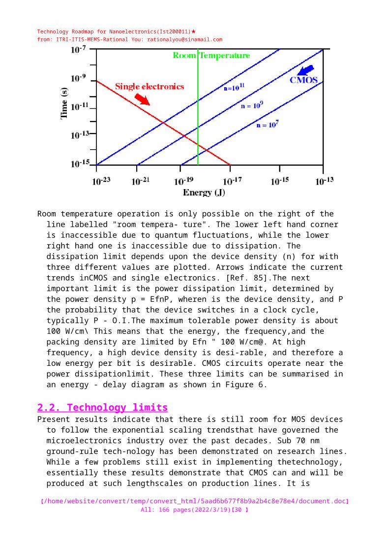
Technology Roadmap for Nanoelectronics(Ist200011)★from: ITRI-ITIS-MEMS-: [email protected]
SiGe ITD: a) band diagram with VD=0.5 V applied bias, andb) measured I-V characteristics on low n-doped semi-insulating Si-substrate inforward direction [Ref. 134].Calculations on the device capacitance showed that lTDs have a much higher capacitance(C = 22 ff/pm@- [Ref. 134]) than RTDs (C = 4 ff/pm@ due to the thinner tunnelling layer.
3.2.2. Resonant Tunnelling Diode Resonant tunnelling diodes (RTD) is also device concept whose inherent multistability allows for
very com-pact circuit, and its inherent speed paves the way for GHz operations. The basic concept of a RTD is illus-trated in Figure 11, Negative differential resistance (NDR) is produced by a double barrier structure havinga resonance peak at voltage V corresponding to resonant tunnelling of electrons through a subband energy,Eo in the quantum @ell between the barriers. Multiple NDR devices may also be produced designing sys-tems with multiple subbands or extra wells.In this case too, the RTD is normally a vertical quantum effect device with the vertical dimensions producedby epitaxial growth and the lateral dimensions produced by lithography. The RTD area determines the cur-rent and hence the power dissipation. All mature RTD devices are produced using III/V semiconductor he-terostructures. There are only a very few demonstrations of Si-based RTDs which result in a limited NDRregime (PVCR = I.I @ 300 K, l= 5 kA/cm@, [Ref. 170]).
Figure II: Concept ofa Resonant Tunnelling Device.
The subband energy EQ is approximately inversely proportional to the square of the well thick-
ness. The peak in the I-V curve occurs when the incident electrons match the energy of the sub-band and the electrons resonantly tunnel from the source to the drain.
【/tt/file_convert/5aad6b677f8b9a2b4c8e78e4/document.doc】All: 107 pages(2023/5/6)【30 】
Technology Roadmap for Nanoelectronics(Ist200011)★from: ITRI-ITIS-MEMS-: [email protected]
3.2.3. Tunnel Diodes Performance III/V RTD device technology is now mature with man@ demonstrations of circuits. These are the
first quantum transport devices to have made it into production. The RTD design depends on the specific application in question. To reduce the power consumption, one of the objective is to produce the mini- mum valley current density possible at a low voltage. On one side the peak to valley ratio (PVCR) must be large enough to allow an appropriate memory or logic function with a reasonable noise margin. On the other side the RTD switching time depends on the RC time constant of the device and therefore the RTD charging time is determined by its peak current density. Hence there is a trade-off between high speed and low power in the design of the circuits. For high speed logic applications, peak current densities greater than 10 kA/cm@ are required allowing a clocking frequencies of 6.25 GHz to be compared with low power TSRAM where the peak current densities are <0.l6 A/cm@ resulting a maximum clocking frequency of 592 kHz [Ref. 164]. Up to now, III-V RTD have demonstrated the following results: @ 80 GBit/s optoelectronic delayed flip-flop [Ref. 187]. @ 50 nW TSRAM cell with a 150 }im." footprint (200x lower power than GaAs SRAM) [Ref. 218]. @ generic logic circuits operating at 12 GHz with 20 pm minimum feature size [Ref. 231]. @ memory circuits [Ref. 226] @ multivalued logic circuits [Ref 144] @ monolithic 4-bit 2 Gsps analogue to digital (ADC) converters [Ref. 31]@ 3 GHz clocked quantisers with 40 dB spur free dynamic range@ 40 GHz static binary frequency dividers [Ref. 216]@ 2 GB/s photodetectors with low switching energies of 30 ffIn comparison to III/V RTDs, the technological status ofSi/SiGe lTD's and RTD's is in its infancy. Atroom temperature, high current densities (> 5 kA/cm@) are available in both type of Si based tunnel diodes,but a significant PVCR has been achieved only with lTDs [Ref. 56,185]. On the other hand the ITD bar-rier is much thinner than the RTD one and hence more critical against technological fluctuations. In addi-tion, a high temperature annealing process for dopant activation and its diffusion is necessary in lTD's, inorder to achieve a good PVCR at a high current density.The better speed performance of SiGe-lTDs in comparison to InP-based RTDs can be determined bymeasuring SiGe-lTD's (from 45 MHz to 45 GHz) and comparing it RTDs with the same layout (A =3x20 ILLrn@) [Ref. 134]. The extracted conductivity corresponds to the DC-data gp = dl/dV. In compari-son with an inP-based RTD with the same device layout, the SiGe-lTD's are about 15 times slower (Fig.12). This reduction is due to the high capacitances caused by the very thin undoped layers between thed-doping layers. 1001@.
voltage (V) *@
Figure 12: Oscillation Frequencies for ITD and RTD.
【/tt/file_convert/5aad6b677f8b9a2b4c8e78e4/document.doc】All: 107 pages(2023/5/6)【31 】
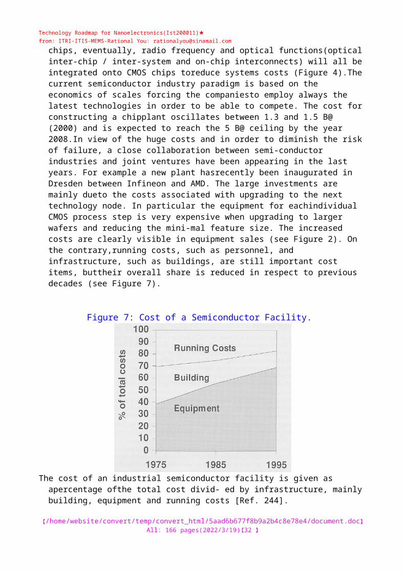
Technology Roadmap for Nanoelectronics(Ist200011)★from: ITRI-ITIS-MEMS-: [email protected]
Maximum oscillation frequency relatively to the peak- and valley-voltage of the SiGe-lTD's andof an InP-RTD [Ref. 134].
In Table 6 the trade-offs between some of the important parameters in RTD designs for logic and memo-ry applications are summarised.
Table 6: Comparison of Tunnelling Devices ParametersParameter High
SpeedRTD logic
Low powermemory
RTD ScaledRTDs SiGeRTD SiGeITD
Demo Forecast
Demo Forecast Demo Demo Demo
Peak to Valleycurrent ratio
4 @ 3 2 3 3 1.2 3.5
Peak current density(kA/cm2)
40 ' 101 0.0002 1 0.0001 10 0.4 17.5
Minimum featuresize [ Urn]
2 1 0.21 0.5 1 0.2 0.05 100 6
Peak Voltage [V) 0.35 1 0.16 0.2 0.2 0.2 0.4 0.3Maximum
clockingfrequency [GHz]
12.5 6.25 592 56.8 6.25 0.5
RTD time constant[ns]
0.02 0.04 422 1 4.4 0.04 0.5
[Ref 164]@ [Refl64]
1 [Refl64] [Ref 164] [Ref 170] [Ref 56,134]
3.2.4. Concepts for Three Terminal Resonant Tunnelling devices Since RTDs are two-terminal devices the requirement of isolating different logic circuit stages has
moti-vated the investigation of three terminal devices, i.e. resonant tunnelling transistors, in order to combineelectronic amplification of a transistor and the inherent multistability of RTDs. In recent years the follo-wing approaches have been demonstrated:@ hybrid microelectronic/nanoelectronic device concept using monolithically integrated RTDs togetherwith conventional transistors, such as heterostructure field-effect transistors (Figure 13 a,b) [Ref. 38] orheterostructure bipolar transistors [Ref. 140]. The relative technological maturity of this approach enablesthe design of various digital logic, memory and analogue circuits and is therefore the "work-horse" toexplore novel circuit architectures.@ vertical resonant tunnelling transistors composed of an RTD with a surrounding Schottky gate to mo-dulate the cross section of the device by means of the gate voltage dependent depletion region (Figure 13c,d) [Ref. 200]. With respect to practical circuit design this approach has advantages over RTD-HFET con-cepts where HFET and RTD I-V characteristics have to match, e.g. the transistor current with respect tothe RTD peak current. Thus, the transistors must be designed in a narrow window of device properties. Ina three-terminal resonant tunnelling device the
【/tt/file_convert/5aad6b677f8b9a2b4c8e78e4/document.doc】All: 107 pages(2023/5/6)【32 】

Technology Roadmap for Nanoelectronics(Ist200011)★from: ITRI-ITIS-MEMS-: [email protected]
matching between RTD and FET is inherently fulfilled. Aninteresting feature for future investigations is the increase of the current modulation with shrinking mesaareas. Further optimisation is needed to obtain an input-output voltage level compatibility.Double-Electron Layer Tunnelling Transistor (DELTT) with an entirely planar structure [Ref. 150]. Thisdouble gate device exhibits an I-V characteristics similar to the vertical RTT but the tunnelling processoccurs between two-dimensional electron gases (2DEGs) perpendicular to the direction of the current flow
(Figure 13e, back control gate is omitted for clarity). The 2DEGs are formed in a AIGaAs-GaAs doublequantum well. By means of two depletion gates the source makes electrical contact to the top quantumwell only, while the drain contacts the bottom quantum well. Thus, tunnelling across the barrier betweenthe quantum well is the only possible way for the electrons to reach the drain region. Resonance conditionis obtained either by shifting the Fermi energies in the source/drain regions via the drain-source voltage orby modulating the electron density of the 2DEGs by the gate voltages. The double gate structure (top andback gate) allows the implementation of unipolar complementary circuits. First prototype devices andbistable memory circuits demonstrate the operation at or below 77 K, though rapid progress indicates thatroom temperature operation is achievable. Despite the simple planar structure a drawback in regard tolarge-scale integration is the difficult flip-chip processing scheme.
W/L=120/1, ARTD=40um2, Top: VGS(mmi)=0.6V, Step-0.1 V
Top DfpletlonOM<__-_ @@@"
0,20,40,60,81,01,2drain-source voltage UDS WConduction Band
Back DipMlonBack-Gate Gate
Figure 13: Concepts for three terminal tunnelling devices(a) fully 3D-integrated Resonant Tunnelling Diode Heterostructure Field-Effect Transistor(RTD-
HFET) and
(b) Vertical Resonant Tunnelling Transistor (VRTT) on GaAs. Both devicesshow a gate-controllable drain-source current with the typical RTD I-V characteristics
【/tt/file_convert/5aad6b677f8b9a2b4c8e78e4/document.doc】All: 107 pages(2023/5/6)【33 】

Technology Roadmap for Nanoelectronics(Ist200011)★from: ITRI-ITIS-MEMS-: [email protected]
(c and d).
The Double Electron Layer Tunnelling Transistor (DELTT) is a planar (e).
3.2.5. Major Challenges and Difficulties for TDs A problem is the extreme sensitivity of the device characteristics to the layer thickness as the
tunnelling cur-rent depends exponentially on the thickness of the tunnel barrier. In the last years, the progress has beenmade to precisely control the growth of the double barrier structures. Investigations for 2" wafers (InP-based RTDs) show that with shrinking minimum feature size the fluctuations in the peak current can bedirectly attributed to an RTD area variation caused by the increasing impact of lithography and etching onlateral dimensions. The peak-voltage and peak-current homogeneity are better than 2.7% and 5.1%,respectively, while the reproducibility is within 6.9% and 9.4%, respectively [Ref. 134]. The peak-voltageis independent of the size of the device area. The variation due to fluctuations in the MBE layer stack isless than 1.2% over a quarter of a 2"-wafer indicating that the influence of MBE layer data was overesti-mated in the past. Recent GaAs RTDs work [Ref. 39] shows that III/V technology fulfils the requirementsfor a large-scale integration of RTD devices. However, the remaining big challenge remains to transfer theprocess technology to LSI production. Unless this is achieved, RTDs will remain a niche product for highspeed switching, digital signal processing, ADC, DAC, etc. where costs/function is of minor relevance.Lateral device scaling to sub-mm feature size is necessary to reduce power dissipation during the switchingprocess in logic circuits and in the bistable state of RTD-memory cells. This is especially important forGHz logic circuits requiring high peak current density devices, where, the overall power dissipation limitsthe integration density. The lateral scaling depends on the lithographic resolution and on the circuits' capa-bility to tolerate local device parameter variations, similar to conventional microelectronics with nm-fea-ture
【/tt/file_convert/5aad6b677f8b9a2b4c8e78e4/document.doc】All: 107 pages(2023/5/6)【34 】
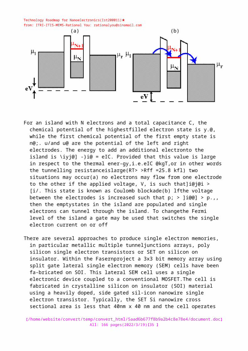
Technology Roadmap for Nanoelectronics(Ist200011)★from: ITRI-ITIS-MEMS-: [email protected]
sizes.The ability to wire devices is currently limited by large contact areas and the lack of multilayer intercon-nections. Here, planar processes may be a step towards fabricating circuits with a reduced complexity.Otherwise RTD circuit designs will be less area efficient than comparable FET design.For millimetre wave oscillator applications, high output power in the NDR-regime from the RTD deviceis needed. At present the output powers are in the order of}iW and would require improvements (> mW).Si/SiGe lTDs show potential for Si-based digital circuits. A major problem oflTD's is the high sensitivi-ty of device characteristics to the effective thickness of the tunnelling barrier during the annealing process.The thermal restrictions in the annealing process limits possible monolithic co-integration with CMOSand unless this can be overcome, lTDs will remain a niche product for low voltage high-speed memoryand logic.Si/SiGe RTDs have been fabricated with a low PVCR of 1.1 at a good current density of 5 kA/cm@ [Ref. 170] offering a new perspective for CMOS co-integration. Si/SiO@ RTDs [Ref, 116] remain under dis-cussion as they would allow CMOS compatible processing and integration of RTDs with CMOS circuits,but problems growing single crystal Si between Si0@ barriers have to be overcome.
3.3. Rapid Single Flux Quantum Logi 3.3.1. Principle of Operation
Rapid Single Flux Quantum (RSFQ) Logic is based upon a superconducting quantum effect, where a fluxquantum is used as a bit. The basic switching elements areJosephson junctions (JJ). As this quantum effectalready occurs at a macroscopic scale, sub-micron lithography is not a prerequisite. RSFQ is the onlyknown technology in which circuit speeds above 100 GHz and power dissipation down to I pW/gate canbe envisaged.There are two basically different technologies to produce RSFQ circuits, depending on whether low tem-perature superconductors (LTS) or high temperature superconductors (HTS) are employed. Due to itssuperconducting principle, a RSFQ device needs cooling and it should be remembered that the operationtemperature of the device is lower than the critical temperature of the bulk superconductor material. Theavailability of adequate cooling systems, which comply with needed specifications (temperature, size,weight, dimensions, etc.) in the limits of reasonable prices, is one of the most important drawbacks for themarket introduction of this technology.
3.3.2. Technology, Critical Dimensions and Performance a) Technology employing low temperature superconductors (LTS) The most mature LTS
technology usually uses superconductor insulator superconductor (SIS) tunnel junc- tions, but also SINIS and SNS technologies, where N stands for normal metal, have been implemented successfully. The usual SIS technology is a three-layer process using Nb as superconductor and AIC)@ as insulator. Nb-based devices must be cooled down to liquid helium temperature. Circuits with several thou- sand junctions, produced with a 3.5 pm design rule, and frequencies up to 40 GHz can be obtained com- mercially. As only magnetic penetration depth limits the critical dimensions, Nb miniaturisation should be possible down to lOOnrn. An alternative is to use NbN as superconductor, where circuits can operate at 10 K. Current circuits have up to 1000 junctions, i.e. one order of magnitude less than the conventional Nb technology. This tech- nology is less mature mainly due to the lack of self-limiting tunnel barriers. For most current LTS circuits 10 mW (@ 4K) of cooling power is sufficient. In terms of input power this corresponds to about I kfl of electrical power, which makes LTS suited only to large systems where the energy consumption and size of cooling engines is of minor importance or to applications exploring quan- tum effects of superconductors, such as in metrological standards. Very large computers such as the Teraflop / Petaflop (10" and 10" floating point operations per
【/tt/file_convert/5aad6b677f8b9a2b4c8e78e4/document.doc】All: 107 pages(2023/5/6)【35 】

Technology Roadmap for Nanoelectronics(Ist200011)★from: ITRI-ITIS-MEMS-: [email protected]
second, respectively) computer, are exam- ples of the first case. They would consume enormous amounts of power if fabricated in silicon, while the use of LTS reduces the cooling problem and offers a more compact layout. b) Technology employing high temperature superconductors (HTS) HTS technology uses mainly YBCO (or other 123 cuprates) as superconductor and mostly PBCO, or a doped variant, as insulator. In order to further reduce the parameter spread, junctions with a interface engi- neered barrier are also investigated. Presently, mostly simple circuits, such as shift registers, with less than30 junctions have been demonstrated to operate at clock frequencies in the order of 40 GHz and at tem-peratures below 50 K. An example is a delta-sigma modulator, also a simple circuit, operating at 170 GHz.This is two orders of magnitude smaller complexity than current LTS technology. Due to the fact thatYBCO is an anisotropic material, the fabrication is far more complex than with LTS. There are diversetechniques to produce HTS Josephson junctions, such as using the interface of bicrystals, c-axis micro-bridge and ramp type junctions. Which fabrication method will be chosen is not clear as all of them havepros and cons. For example, ramp type junctions have the best reproducibility, while microbridge systemsare more easily scalable, a factor that may become important in the future.The advantage of HTS in respect to LTS is that it is supposed to operate at higher frequencies (up to 500GHz) and higher temperatures (50K), when the circuits will be produced with a 500 nm groundrule. Thisdoes not imply that a clock will be used at this speed, as at these speeds circuits are likely to operate blockasynchronous and probably completely asynchronous [Ref. 98]. The feature size 500 nm is limited by themagnetic penetration depth. The higher temperature allows for less extensive cooling efforts, while the
higher frequency may open a window for new applications. As HTS circuits will be operated at higher tem-peratures than LTS it is expected that the risk of bit error rate increases. Measurements of these values havenot been performed.
3.3.3. Major Challenges and Difficulties for RSFQ In principle, RSFQ circuits can operate at frequencies up to theTHz regime. From a client's point of
view,the important issue is not only the frequency of the RSFQ circuits, but also the input / output operationfrequency to the outside world. In this respect, a challenge is to find appropriate interfaces to Si-CMOS orother devices that can benefit from the potential of very high-speed circuits.For LTS, the design and implementation of VLSI circuits with more than 105 gates per chip is a majorchallenge. For acceptable operating margins, very narrow spreads of junction parameters will be needed(probably in the region ISigma < 3-5%). Apart from the technological problems, economical considera-tions may produce some drawbacks. In view of the fact that the market for applications requiring VLSI,such as very high performance computing, is small, it is not evident if the large financial investments nee-ded to upgrade facilities to produce VLSI circuits would pay off.HTS technology seems to be about 10 years behind LTS. In the short term, i.e. in the next three years, themain challenge is to fabricate and test circuits in the order of 100 junctions. For this to be achieved, majorefforts must investigate the development of junction technology with a small parameter spread (desirableISigma < 8%), the development of small inductances, reliable resistors and the reproducible connection ofthese circuit elements. In the medium term (5-8 years), the feasibility of small circuits operating at frequen-cies of around 100 GHz should be definitely demonstrated and integrated into a demonstrator / application.The main obstacle for a broad implementation of superconducting electronics is the need for cooling. Mostpotential clients are reluctant to accept liquid cryogenic cooling, because it is expensive, mostly not reliableenough and requires bulky compressors. Therefore market acceptance will be strongly linked to the avai-lability of low cost, highly reliable and compact cooling systems. Technical progress has been made in pro-ducing improved cryocoolers, such as Joule-Thomson,
【/tt/file_convert/5aad6b677f8b9a2b4c8e78e4/document.doc】All: 107 pages(2023/5/6)【36 】
Technology Roadmap for Nanoelectronics(Ist200011)★from: ITRI-ITIS-MEMS-: [email protected]
Stirling or pulsed tube refrigerators, but at presentthere is no real market and hence no serious investment in developing cryocooler systems.To be economically competitive, HTS must be operational with a single stage Stirling and Joule Thomsoncryocoolers. In terms of performance, this requires that the RSFQ circuit must be operational below 40 Kand requiring at a maximum 100 mW power dissipation.Nb-based circuits require cooling at 4 K. These temperatures can be achieved employing liquid helium coo-ling or using a three stage cryocooler, such as a two stage Gifford-McMahon plus a Joule Thomson stage.All options are expensive and are bulky. Financially, a major progress would be obtained if a two-stage sys-tem could be used. NbN-based or other LTS superconductors technology may fulfill the requirements to beoperational at 10 K, but the technology is not very advanced, in between Nb-based LTS and HTS.
3.4. Molecular Nanoelectronics In the following, the term "molecular nanoelectronics" is used to distinguish devices switching at
the sin- gle molecule level compared to bulk based molecular electronics, which have found numerous applications as liquid crystals in displays, dye lasers, light emitting diodes or plastic transistors. Already in 1974, Aviram and Ratner predicted that single molecules with a donor spacer acceptor structure would have rectifying properties when placed between two electrodes and could be used as functional elec- tronic elements. [Ref. 14]. Such a rectification behaviour was first observed in molecular monolayers sand- wiched between two metallic electrodes [Ref. 70] . This type of measurement is produced using Langmuir- Blodgett film or self assembly techniques and involves a macroscopic number of molecules. Electrical measurements of individual molecules have been possible since the invention of the scanning tunnelling microscope and have been demonstrated on C60 fullerenes and a few other molecules. In addition, progress producing nanoscale junctions has permitted the performance of planar two terminal electrical measure- ments. Junctions with dimensions as low as 5 nm [Ref. 41] can be manufactured in a reproducible manner with e-beam lithography, and nanojunctions down to 2 nm have been obtained by electromigration [Ref. 152]. As the distance between the electrodes is in the range of the dimensions of a number of appropriate designer molecules, the search for appropriate functional molecules has just begun. Hybrid molecular electronics holds the promise of self-assembly of circuits, both on a massive scale and cheaply, using chemical or biological reactions and to match the ultimate densities of CMOS [Ref. 108]. For molecular devices to become logic and memory elements of circuits the aim is to achieve bit densities of 10" bits/cm\ to reduce switching cycle times to a few ps and to limit the energy per bit cycle to 10 meV. Otherwise the heat dissipation is too high and a cooling system has to be integrated. Molecular nanoelec- tronics is far from these targets, but has the potential to produce sub-nm sized functional devices in a bot- tom-up way without suffering the inherent tolerance problems of a lithographic top-down exposure me- thods approach [Ref. 73]. Manufacturable solutions may be of hybrid nature built on top of a CMOS chip [Ref. 229] with the CMOS chip providing the input / output to the macroscopic world. Alternatively molecular nanoelectronics may be optically interconnected to other systems.
3.4.1. Electric-field based molecular switching devices The basic concept is to control the transconductance of a molecule by an electric field. Ideally, one
would use the central part of a molecule for functions (switching, RTD, transistor, rectification, etc.) while theendgroups would provide the linking through a self-assembly mechanism. Diblock copolymers, for exam-ple, may be self-assembled into chains and purified to very high yields. Thiol endgroups would anchor thecopolymers to metal electrodes.The mechanism for the functional operation can be very diverse. As already indicated, attaching elec-trophile and electrophobic groups to either end creates a donor spacer acceptor structure that induces a rec-
【/tt/file_convert/5aad6b677f8b9a2b4c8e78e4/document.doc】All: 107 pages(2023/5/6)【37 】

Technology Roadmap for Nanoelectronics(Ist200011)★from: ITRI-ITIS-MEMS-: [email protected]
tifying behaviour, Aviram [Ref. 15] proposed a number of molecules that would switch between conduc-ting and insulating states by oxidation / reduction. For example, tetrathiafulvalium (+) has only a partiallyfilled highest occupied molecular orbital and offers free states for conduction, while tetrathisfulvalene is aninsulator because the highest molecular orbital is completely filled (Figure 14). Here, the switching beha-viour would be based upon the fact that electrons can tunnel only in the case of empty states. In a certainway this is the molecular analogue of the Coulomb blockade principle in junctions.Experimental results include current voltage measurements from single designer molecules, such as the rec-tification properties of a benzene ring attached to two gold electrodes using S atoms (Benzene-1, 4-dithi-olate) [Ref. 184], More complicated structures have been synthesised and it could be shown that the rota-tion of a single bond of 71 orbitals allows the change of conductance by over 6 orders of magnitude,providing a switching mechanism in a polymer chain [Ref. 183]. First "coulomb blockade" characteristicswere demonstrated using self-assembled gold particles on top of a,a'-xyldithiol (XYL) molecules on anAu(lll) surface [Ref. 10]. The second electrode was a STM tip and a Coulomb staircase function wasdemonstrated at room temperature. A field effect transistor action could be observed by placing a semi-conducting carbon nanotube across two electrodes with a controlling back-gate [Ref. 206]. Clear Coulombblockade steps and single electron effects were demonstrated at room temperature. These experimentsdemonstrate basic transistor principles but a complete three terminal transistor device as defined in thisroadmap has yet to be demonstrated.
Figure 14: Transport through a Molecule
A conjugated molecule can switch its conducting behaviour when few electrons are added or removed through an oxidisation or a reduction of the molecule, respectively. In an energy band description the conduction depends upon the number of electrons in the hi@hest-occupied-molec- ular-orbital (HOMO), which is represented by arrows in the above picture. Similar to a Coulomb blockade effect, electronics states in the (HOMO-LUMO) gap of the molecule can be introduced and be put in resonance with the Fermi level of the electrode. In the above scheme electrons could flow from one molecular chain to the other applying a perpendicular electric field[Ref. 13,52].Using an STM, bond rotations in molecules can be studied to determine how they adapt or can switchtheir state. Such recognition of conformation and adaptation of individual molecules are interesting as con-formational processes are used in natural systems and
【/tt/file_convert/5aad6b677f8b9a2b4c8e78e4/document.doc】All: 107 pages(2023/5/6)【38 】
Technology Roadmap for Nanoelectronics(Ist200011)★from: ITRI-ITIS-MEMS-: [email protected]
form a basis for molecular switches [Ref. 110]. Inaddition, molecular systems such as fullerene based systems can be incorporated in two and three termi-nal devices and interesting electronic characteristics can be obtained, i.e. macroscopic quantum state in abucky tube [Ref. 205].Research in self-assembly for electronic purposes has involved a drive to optimise the molecular chainlength, to functionalise the molecules and to define molecular patterns on the scale of tens of nanometers,such as in the case of printing techniques. In this respect supra-molecular concepts have been introducedin the design and self-organisation of grid-like metal co-ordination arrays using molecular systems [Ref.128,189]. However, the assembly of devices and arrays may be different from current approaches. Forinstance at the macroscopic scale, chemical interactions are used for three dimensional self-assembly of mil-limetre scale components [Ref. 209] or DNA is used to create a binding interaction between nanocrystalsof colloidal metals in solution (or potentially at a surface) [Ref. 147].
3.4.2. Alternative molecular components Electromechanical SwitchingElectromechanical switching at the molecular level is based on the
controlled deforming or reorienting ofa molecule rather than moving the electrons on the molecule. For example C@ can be used as a single mo-lecule electromechanical amplifier by pressing the bucky ball with a STM tip. The controlled vertical defor-mation of the Cgo cage produces the mechanical modification of resonance tunnelling bands. Although theamplification principle has been demonstrated only at low frequency (lOHz), the intrinsic speed of such adevice is limited only by the vibrational frequency ofCgo at over 10 THz (10"Hz). A complete memorybased upon electromechanical transistors could be constructed using an array of metallic nanocantilevers
[Ref. 107]. Future circuits with 10" to 10" elements/cm@ cannot be build with mechanical cantilevers, but will require new architecture paradigms. Another mechanical device is the "molecular abacus" using fullerene Cgo as beads, a 0.25 nm high monatomic step as the rod and STM tip as the finger both to reposition (in one dimension) and to count by imaging. The abacus itself has an active area defined as around I nm x 13 nm [Ref. 47,48]. By moving a single atom out or into an atom wire researchers at Hitachi have simulated a two state electronic device of atomic dimensions [Ref. 221]. The device is called an atom relay or molecular relay. Two-state devices based on the change of a molecular conformation can also make a relay such as a rotarner [Ref. 204], Photoactive/photochromatic switching A number of molecules, specifically a number of proteins, may have their electron distribution changed by the absorption of photons to produce switching effects. The biological photochrome bacteriorhodopsin has been suggested as one possible type of molecule for holography, spatial light modulators, neural network optical computing, non-linear optical devices, and optical memories [Ref. 23]. The significance of bacte- riorhodopsin stems from its biological function as a photosynthetic proton pump in the bacterium Halobacterium halobium. A combination of serendipity and natural selection has yielded a native protein ideal for optoelectronic applications. Other examples ofoptoelectronic biological molecules include visual rhodsin [Ref. 23], chloroplasts [Ref. 78] and photosynthetic reaction centres [Ref. 27]. Spin based molecular devices Manganese acetates with total large spin magnetic moments (20 iuuB) exhibit a hysteresis cycle at low tem- peratures. Hysteresis effects, that normally are seen as many particle behaviour, are often the basis for infor- mation storage and the fact that magnetic behaviour is observed at atomic or molecular scale is interes- ting for downsizing memories [Ref. 138,186,193]. Molecular Wires Oligomers as such are generally very poor conductors and for wiring the applicability of a tunnel transport regime is under investigation. For building circuits molecules with a good conductance must be synthe-sised. Generally speaking, the inclusion of delocalised electrons on aromatic and acetylene
【/tt/file_convert/5aad6b677f8b9a2b4c8e78e4/document.doc】All: 107 pages(2023/5/6)【39 】
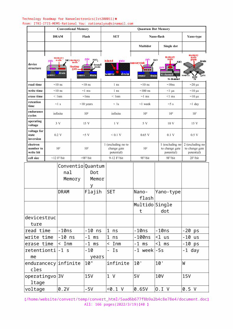
Technology Roadmap for Nanoelectronics(Ist200011)★from: ITRI-ITIS-MEMS-: [email protected]
groups is insuf-ficient for good conducting properties as required by the microelectronics industry in circuits. In such com-pounds, the delocalised 71 electrons occupy the "homo" (highest occupied molecular orbital) fully and inprinciple the extra electron for the electrical transport must be added to the few eV higher "lurno" (lowestunoccupied molecular orbital) level. Alternatively, for small distances (few 10 nm) the possibility of tunneltransport (current of less than nA) could be envisaged by not injecting an electron on the Lurno, but tun-nelling through it. In the first case, the compound acts as a semiconductor and good conducting proper-ties could be obtained by doping the system. In the latter, the challenge is to optimize the molecular wirefor a tunnel transport regime.Metallic wire like properties can be observed with carbon nanowires, due to their band-structure. Thesecompounds seem promising, but ways must yet be found to connect them, through conducting junctionsat specified positions, to the active switching element. One option could be via RNA synthesis and wiring,
3.4.3. Molecular modelling The models employed in molecular electronics to determine the "electric" properties of molecules
are ingeneral less accurate than calculations of electronic structure in quantum chemistry. Therefore actual workexploits quantum chemistry methods to provide reliable predictions needed for device fabrication.However, at the moment only very little work has been done on models that predict the actual conduc-tance of families of molecules that may exhibit useful functionality for device implementation.Conductance studies investigate open systems with a flow of particles, which make the quantum treatmentsignificantly more difficult than in the case of confined states. An example of a hybrid structure of interestis an oligo-thiophen molecule connected on one side to an hydrogen passivated Si (100) surface and on theother side to an STM tip (see Fig. 15, next page).
Figure 15: Scheme of a Hybrid Metal-Molecule-Semiconductor Structure.
An oligo-thiophen molecule is attached to a H-passivated Si(IOO) surface and picked up by anSTM tip [Ref. 28] .For practical purposes, theory must not only describe the intrinsic properties but must also integratechemisorption information to predict how the molecules must be attached in any conceivable structure forinformation processing and what the effect will be on the substrate. Many proposals for molecular devicesexist, but seem to be too optimistic, as they are based on extremely qualitative arguments. For example,there are several proposals for devices exploiting potential barriers within molecules [Ref. 214], but nodefinitive demonstration of the existence of such barriers is yet available. In this case, the use of densityfunctional theories or pseudopotential approaches are under investigation to define the potential profileseen by an electron along a molecule and on this way to define a contact barrier at each side of the con-tact.
【/tt/file_convert/5aad6b677f8b9a2b4c8e78e4/document.doc】All: 107 pages(2023/5/6)【40 】

Technology Roadmap for Nanoelectronics(Ist200011)★from: ITRI-ITIS-MEMS-: [email protected]
Due to the difficulty in performing experimental measurements, the solution might be using moreaccurate numerical simulations, which are explained in the following.Quantum chemistry methods are already employed on some microelectronics problems [Ref. 79] and semi-empirical quantum chemistry methods are used to study molecular transport [Ref. 87]. Ab initio andmolecular modelling methods have been applied for many years to the design of molecules in the phar-maceutical and fine chemical industries and similar tools are employed for designing molecular electronicsand self-assembling systems.Non-equilibrium transport simulations in molecular electronics are now relying on the direct calculationof the energy levels (band structures). This theoretical approach started 15 years ago, but practical calcula-tions employing accurate electronic structures for nanowires and molecular devices are only now emerging[Ref. 223] and fundamental problems on quantum mechanical transport calculations still remain, parti-cularly at the molecular level. Current transport simulations are self-consistent for the unperturbed atom-ic and molecular constituent systems, but do not account for self-consistency under charge injection.Furthermore, correlation effects in charge transport, that are critical for the charging of quantum dots andfor molecular systems, cannot be simulated as explicitly correlated methods remain beyond the computa-tional reach for most systems of practical interest.Density functional methods for charge transport problems face difficulties in far-from-equilibrium appli-cations where excited states must be treated accurately, whereas density functional methods are strictlyapplicable only to ground state problems. Time dependent density functional theory for molecular systemsare actively investigated, but the prediction of molecular electronic states can be more than an electron voltin error, an unacceptably high level for accurate molecular level prototyping. Alternatively quantum many-body methods would be more accurate, but remain beyond todays computational possibilities. Currently,computational scientists investigate electron transport through zero-dimensional systems and computeconductance of molecules with their real molecular orbital structure for a wide range of conditions, butthey face the problem of very few experimental data of electronic functionality at the molecular scale. Asdevice and circuit applications emerge, operating ranges will become better defined allowing researchers toconcentrate on building accurate and efficient models for specific transport mechanisms, without relyingon a fully ab initio description of a system.
3.4.4. Major challenges and difficulties for molecular electronics Molecular electronics is behind other alternative concepts discussed in this document as none of the
fol-lowing issues have yet been demonstrated:@ self-assembly of single devices at reasonable (or small) integration densities let alone integration with con-ducting molecular wires;@ appropriate yield of devices from chemical or biological reactions for fabricating or manufacturing of cir-cuits;@ high data bandwidths for interconnects;Only few molecular demonstrators exist yet that would be suitable as circuit components, but some novelarchitectures discussed in chapter 5 are applicable to these molecular electronic systems.
3.5. Spin Devices All spin-transport devices are based on the effect that the magnetic spin of electrons can be
manipulated in(opto-) electronic devices by magnetic fields or applied voltage. The domain of spin-transport devices iscommonly referred to as magnetoelectronics or spintronics. The spin-transport effects are most widely usedtoday in magnetic metallic devices such as read heads for Hard Disk Drives and in Magnetic RandomAccess Memories (MRAM). These device structures comprise magnetic thin films, the magnetic orienta-tion of which can be changed with applied magnetic fields. In case of non-volatile MRAM the orientationwill be preserved until the bit is switched again. Hence, a locally generated field performs the writing of amagnetic bit, by
【/tt/file_convert/5aad6b677f8b9a2b4c8e78e4/document.doc】All: 107 pages(2023/5/6)【41 】
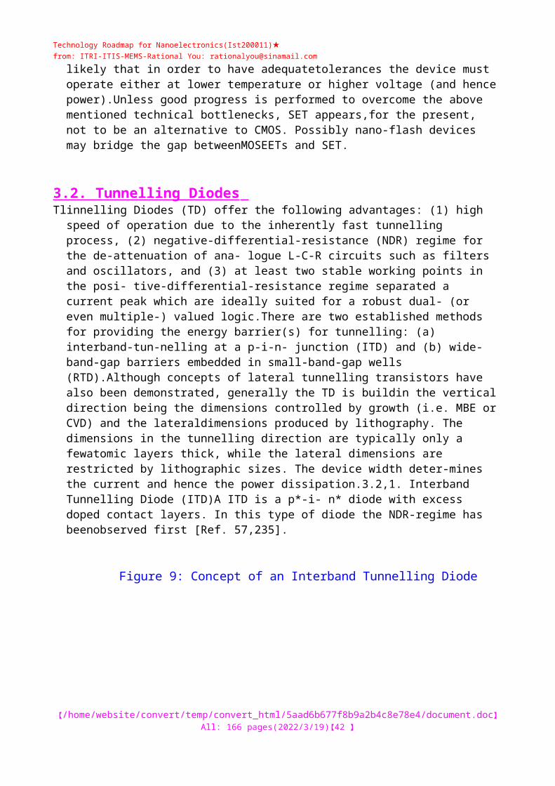
Technology Roadmap for Nanoelectronics(Ist200011)★from: ITRI-ITIS-MEMS-: [email protected]
currents in the vicinity of the magnetic structure. The reading principle of magnetic bitsis based on the discrimination between two distinct magnetic states in the device by measuring the (tun-nel-resistance in the device. In future generations semiconductor-based spin-injection components areexpected to play a significant role. The different device models will be discussed below.In principle, spin-transport devices could be used also as logic gates but so far such demonstrators [Ref. 44]are in their infancy and it is not clear if they comply with all elements necessary for reliable informationprocessing. Hence, only memory applications will be discussed in the following.
3.5.1. Spin Valve Devices In spin valves - a magnet / metal / magnet heterostructure - a difference in electrical resistance
exists forparallel or anti-parallel orientations of the magnetic layers. When one of the magnetic layers is free to moveits magnetisation orientation with the other one fixed, an externally applied field can bring the device inparallel or anti-parallel magnetic state. When used as a memory device, the orientation of the free layer canbe switched but experiences hysteresis, hence remembers the orientation of the last applied field.A typical spin-valve consists of a thin film stack of several layers of which the functional part is a soft mag-netic layer, that rotates easily at low fields, and a harder magnetic layer, that remains fixed up to high fieldvalues. Both magnetic layers are spaced by a noble metal. The layers are 5 to 20 nm thick each. When avoltage is applied, the electrons move randomly and are scattered many times across the interfaces of thetri-layer. This scattering has generally no influence on the spin orientation, as the spin-flip length is largerthan the mean free path. The resulting electron flow can be understood if we consider the current for eachof two spin orientations and sum them up.
Ferromagnetic thin filmMetal spacer layerFerromagnetic thin film
Low resistance path for one(majority-spin) electron spinorientation
Figure 16: Scheme of a Spin Valve
Higher resistance path for bothelectron spin orientations.
The concept of a spin valve transistor is represented in its simple three-layer structure. Additionallayers needed for the correct operation of the device are omitted for clarity. The current flows par-allel to the layers for a voltage applied on the extremes. The large white arrows in the ferromag-netic film indicate its overall magnetic orientation. The white and black lines represent the tra-jectories of two electrons with opposed spins, (the electron spin orientations represented by smallwhite arrows) [Ref. 49].First, assume that the magnetic moments of both ferromagnetic films are aligned and a voltage is appliedthat makes the electrons move from left to right in Figure 16. A majority-spin electron in one ferromag-netic layer is also majority in the other. An electron moving with the same spin orientation as the majori-ty-spin, experiences a relatively low resistance to travel through the tri-layer. On the contrary, the minori-ty spin electrons would be highly scattered at the interfaces and the bulk of the ferromagnetic layer, hencefeeling a high resistance. As by definition there are more majority
【/tt/file_convert/5aad6b677f8b9a2b4c8e78e4/document.doc】All: 107 pages(2023/5/6)【42 】

Technology Roadmap for Nanoelectronics(Ist200011)★from: ITRI-ITIS-MEMS-: [email protected]
spin electrons minority, there is a highelectron current.
When the magnetic films have opposing magnetic moments, a majority electron in one magnetic film is atthe same time minority in the other film and the density of spin up and spin down electrons is the same.Therefore, independently of its spin, a moving electron would always be subject to spin dependent scat-tering in either one of the two magnetic layers. No preferred electron spin "channel" would be observed.The increase in resistance when going from parallel to anti-parallel magnetic state can achieve up to 18%at room temperature and it is often referred to as the Giant Magnetoresistance effect (GMR).In view of its operation principle this type of device is called a "spin valve" and it represents one possibleway to implement the elementary cell of a MRAM.
3.5.2. Tunnel Junction Devices In a tunnel junction (TJ), an insulating layer separates two ferromagnetic layers. An electronic
current canpass tunnel through the insulating barrier by applying a voltage. The tunnelling current, which flows per-pendicular to the layers, depends on the relative orientation of the magnetisation of the two ferromagne-tic layers. If the magnetic orientation of the two ferromagnetic layers is aligned, there is a high probabilitythat the electrons can tunnel, hence the resistance is low. On the contrary when the orientation of the twoferromagnetic layers are anti-parallel, the resistance is high. The difference in resistance for parallel to anti-parallel magnetic moments can exceed 49% at room temperature. The thickness and the materials choiceof the insulating layer controls the resistance of the device (which can be varied by several orders of mag-nitude). By reducing the thickness of the tunnel-barrier to about I nanometer, the resistance of the mag-netic TJ device can be on the order of 10 to 100 Q-mrn@ making it perfectly suitable for deep submicronintegration. Furthermore in TJ devices the current flows perpendicular to the layers, permitting a densearrangement of the memory cells. Much like the spin-valve the magnetic TJ can be exploited as a cell forstoring one bit placing the magnetic tunnel-barrier at the intersection of two orthogonal lines. A completeMRAM can be set up as a two dimensional array, where the individual cells are at intersections of wordand bit-lines providing the necessary local magnetic fields [Ref. 49].
Ferromagnetic thin filmOxide spacer layerFerromagnetic thin film
Low resistance state High resistance state
Figure 17: Scheme of a Tunnel function
In difference to a spin valve (Figure 17) the current flows perpendicular to the tunnel junction.[Ref. 49].
3.5.3. Spin injection devices 【/tt/file_convert/5aad6b677f8b9a2b4c8e78e4/document.doc】
All: 107 pages(2023/5/6)【43 】

Technology Roadmap for Nanoelectronics(Ist200011)★from: ITRI-ITIS-MEMS-: [email protected]
While the above mentioned all-metal devices have found there way into IC-integration fabs, where theyare getting prepared for embedded memory applications, future generation of spintronic devices will relyon the ability to manipulate carrier spins in a semiconductor. Recent progress in the area of spin-engi-neering in semiconductor structures have given the confidence that spin-ensembles in semiconductors livelong enough and can be driven by voltages to migrate in a coherent fashion over microns distance, evenacross hetero-interfaces. Also, polarised light emission has been demonstrated, generated by spin-polarisedcurrents [Ref. 86,114,115]A condition for most presently proposed semiconductor spin-transport devices is the possibility to injectspin-polarised electrons from a contact into the semiconductor heterostructure. When the spin-injectionprocess is efficient, many different device concepts (including g-factor engineering) can be envisaged thatcould lead to novel computing approaches (e.g. ■■Quantum Computing).The advantage would be to move away from all-metal spin valve devices towards an all-semiconductordevice that could reduce the entry barrier to incorporate spin electronics with traditional semiconductor
technology. In addition such spin devices be could be combined with opto electronics on a single chip. These type of spin devices do not yet exist, but the recent discovery that spin injection into two different families of semiconductors is possible is a breakthrough. The first experiment was based upon BeMnZnSe, a II-VI compound semiconductor. This material is used as a spin aligner to polarise the electrons before they are injected into GaAs. The GaAs device acts as a light emitting diode and spin polarised electrons produce polarised light emission [Ref. 61]. From this emission it can be deduced that the efficiency of the spin injection from the semi magnetic to the magnetic semi-condutor is in the order of 90%, which would be high enough for industrial devices. The drawback is thatthis spin aligner works at low temperature and needs a high magnetic field, and is not suitable for roomtemperature applications.The second approach uses GaMnAs, a III-V ferromagnetic compound semiconductor, as a spin aligner ofpositively charged holes. The holes are injected from the GaMnA@, through a GaAs spacer, into a quantumwell structure that acts as light emitting device [Ref. 160]. An advantage in respect to the BeMnZnSeapproach is that GaMnAs systems can operate at higher temperature if the Mn could be increased.Unfortunately, to date, polarisation measurements indicate a low spin injection efficiency of 2%. The ori-gin of this low efficiency rate is unclear and may be caused by optical selection rules for heavy holes tran-sitions. Other III-V based semiconductors such as GaMnN [Ref. 53] are predicted to be ferromagnetic atroom temperature but this prediction urgently needs experimental verification. A drawback is that thesecompounds are p-type and the hole spin dephasing time is much smaller than that of electrons.
3.5,4. Performance The first generations of MRAM were based upon the anisotropic magneto resistance (AMR) and
laterupon the giant magneto resistance (GMR) effect. They exploit the change in resistance of all metal me-mory cells when their magnetisation states are modified. The resistance is in the order of 10 to 100 Ohmsdepending on the material and the film thickness. The current flow is horizontal to the structure. For highcapacity memories suitable for computer storage a high resistance value is required in order to reduce theread / write dissipation.An advantage of MRAM based on magnetoresistive effects in metallic structures is that they undergo thesame scaling rules as Si-technology. New materials development, such as tunnel magnetoresistance, willimprove density, speed and power performance. Access time is determined by the Si-circuitry and is in theorder of 10 ns.Current commercial MRAM have 200nm cells producing 8% output in resistance change with a clearmemory effect. For a future improvement of the memory circuit additional requirements have to be metsuch as a better control of the interlayer
【/tt/file_convert/5aad6b677f8b9a2b4c8e78e4/document.doc】All: 107 pages(2023/5/6)【44 】
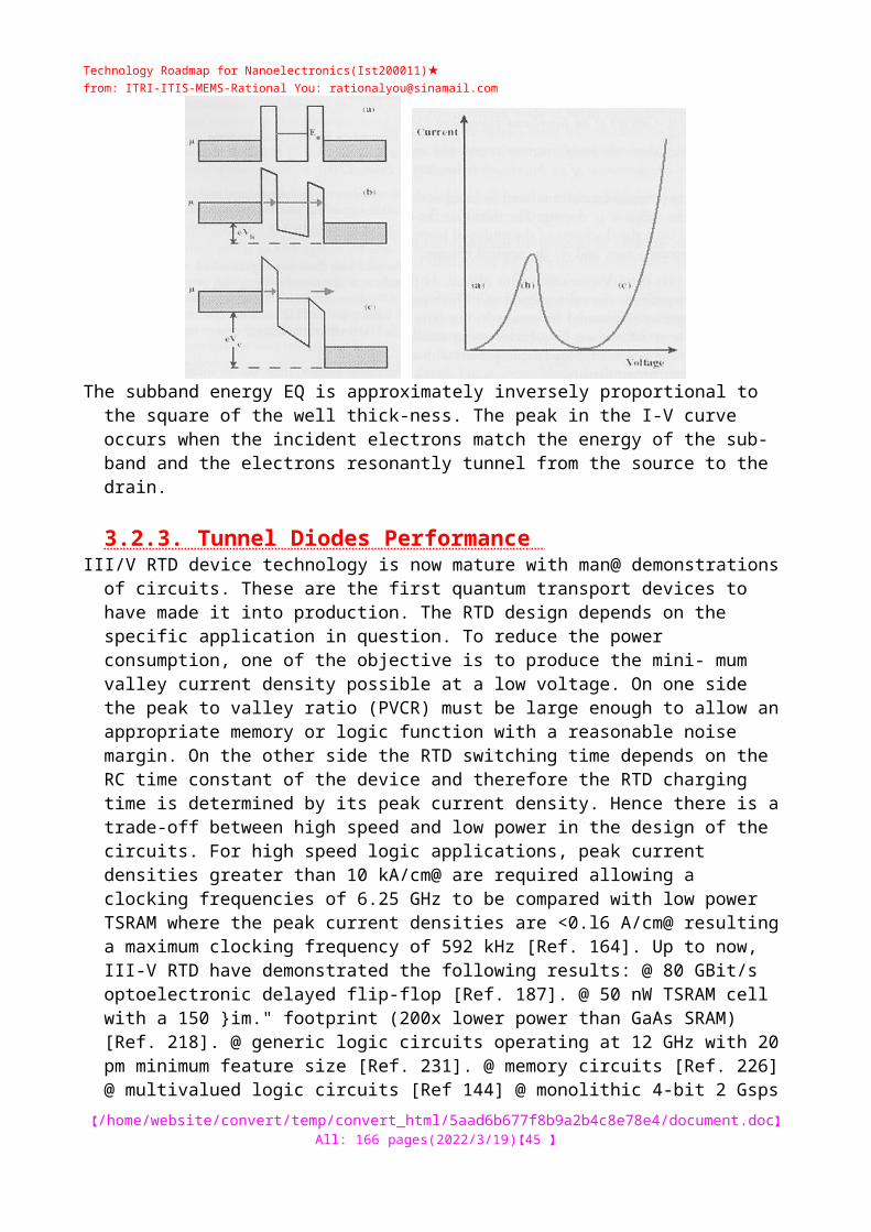
Technology Roadmap for Nanoelectronics(Ist200011)★from: ITRI-ITIS-MEMS-: [email protected]
thickness, thin insulation, a magnetic keeper structure and con-ductor materials with higher allowed current densities (>10@ A/cm@). Analysis shows that sense line widthless than 100 nm and array densities of 5x10* bits/cm@ are possible with GMR. The commercial near futureobjective is to produce a GMR based memories with 4 Gbit/cm@ capacity. The process should be fullCMOS compatible to ensure lowest power, highest reliability and rapid insertion into existing markets. Inrespect to an equivalent semiconductor memory (DRAM), MRAM needs only 2 to 3 metal interconnectlevels resulting in a lower cost factor. Moreover MRAM compact architecture permits to process featuresizes that are I to 2 generations behind DRAM, so that an increase in memory density can be envisaged.The current state of the art of MRAM is compared with other technologies in Table 14 and a forecast forthe year 2006 and 2012 is given in Table 15 and Table 16 respectively.
3.5.5. Challenges and Difficulties Present all metal MRAM concepts will be applicable below lOOnm technology as the underlying
magne-tic effects can be treated as bulk-properties permitting to carry out logic functions using current materials.Below this the technological challenges will be to control the magnetic switching behaviour and micro-magnetism in the nano-scale structures.Magnetoelectronic devices have no inherent electronic gain and require a additional circuity for the wri-ting / reading. The signal read out has therefore to be performed by reading the resistance of an impedancematched device, such as in the case of tunnel junction devices or magnetically modulated devices or inclu-ding a transimpedance systems, such as in spin-valve transistor or spin-injection devices. This disadvantage
against conventional semiconductor technology is compensated by the fact that MRAM circuits have a simple design, basically creating a memory array by crossing to metallic conductors. There is no need to include a single transistor in the memory node, allowing for back-end processing and buried electronics.The memory density is therefore only limited by metal-distance, i.e. the conventional DRAM lines widthrules. When a transistor is part of the magneto-electronic memory-cell, area density can be sacrificed infavour of a larger fan-out or functionality. Multi-value MRAM storage nodes have hardly been addressed,but should be feasible when multiple magnetic states are stable in a multilayer of magnetic material.Besides the all-metallic MRAMs, the integration of magnetic nano-structures and semiconductors in noveldevice structures and the exploitation of minority-majority spin effects offers new perspectives on magne-to-electronics. These include the control of spin-polarised current in components using magnetic field,electric field, or light modulation,The main difficulties related to spin devices are summarised as follows:@ Tunnel Junction Devices: In order to have optimum resistances (of about 50 Ohm) future high densitytunnel junction MRAM will require thin tunnel junctions of the order of a nanometer. The spread of thejunctions must be at Angstrom-level for achieving the uniformity needed for high density. This requires ahigh precision in manufacturing.@ Tunnel Junction Devices: The current bottleneck for reducing the MRAM cell size is limited by the semi-conducting diode / transistor that avoids the shortcuts in the array (blocking diode). For large-scale inte-gration, either the size of the blocking diode must be reduced or alternatively the spin device itself mustperform the blocking function.@ Spin injection devices: Although spin injection into a semiconductor has been demonstrated, it is still tobe proven that the materials and the concept are suitable for room temperature operation and large scaleintegration
3.6. Wave interference devices: Electronic Waveguiding and Quantum 【/tt/file_convert/5aad6b677f8b9a2b4c8e78e4/document.doc】
All: 107 pages(2023/5/6)【45 】
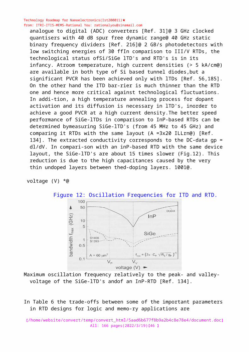
Technology Roadmap for Nanoelectronics(Ist200011)★from: ITRI-ITIS-MEMS-: [email protected]
Interference DevicesSemiconductor heterostructures may define quantum wells for electrons giving sharp energy states
for theelectrons in the directions perpendicular to the heterostructure interfaces. It is possible to fabricate chan-nels for electrons with only one (or a few) eigenenergies (or modes) below the Fermi energy in two of the3 possible directions. Such a structure forms a I-dimensional waveguide similar to a RF waveguide or a sin-gle-moded optical fibre. It is a natural question to ask, to what extent the well-known devices used formanipulating RF radiation or light signals can be rediscovered and employed for electrons in electronicwaveguide devices. Indeed, it turns out that such an analogy is very useful and has given inspiration tomany beautiful and potentially useful electronic devices fabricated by nanotechnologies to match the short(- 40 nanometer (nm)) electron wavelength normally encountered.Electronic waves have a cut-off in electron energy below which no electronic wave can propagate; abovethis energy a single-mode I-dimensional (ID) electronic system is observed until a characteristic energy isreached, above which two transverse modes can propagate. The transmission through such an electronicwaveguide gives rise to a fundamental DC electrical resistance of h/2e@=12.9 kOhm per mode [Ref.219,227]. The macroscopic leads normally contain many modes. The quantum resistance is due to thetransition between this many-mode system to the I D electronic channel in question. Again this is qualita-tively analogous to the matching of free space electromagnetic waves being guided into a square RF wave-guide by a so-called microwave horn.The devices are based on the wave properties of the electrons by controlling the constructive or destructiveinterference of two or more partial waves. For nanoscale devices these effects are generally much more sen-sitive to external electric field variation than the traditional field effect presently used in most electronics.The examples given below illustrate this. A particular bonus of such devices is the possible switching beha-viour connected with the inherent discreteness of the energy spectrum [Ref. 168]. The difficulty in imple-menting such interference devices in commercial instruments is that these devices generally still are onlyfunctioning at very low temperatures (below say 30 K). In order to make the devices useful at room tem-perature requires another leap down in the nanoscale to well below the 10 nm scale.I-D devices may have electrostatic switching properties also at room temperature. These properties areobserved in so-called Y-Branch devices, and are not directly connected to the wave nature of electrons. Thisopens up new switching properties, though similar to the traditional field effect devices, they may turn outto be much more sensitive due to its bistable nature [Ref. 232,234].
3.6.1. The basics of Coherent Switching and Interference An electronic confinement such as in quantum well structures leads to a set of eigenenergies that
can becalculated from the Schrodinger equation. The population of the electron energy states (following the Pauliprinciple) has to be taken into account, which adds extra charge to the quantum well which alters thepotential energy due to capacitance or electron-electron interaction effects. The calculation of eigenener-gies therefore involves a simultaneous and self-consistent solution of the Poisson equation and theSchrodinger equation. The density of electrons and hence the confinement is changed by an external gateand it is necessary to solve the new state self-consistently. In a case where for instance the electrical resis-tance comes out as a delicate balance between two values as for instance at a branching point, biasing a gatein the vicinity lead to large changes in the circuit resistance. Such a switching device does not rely on acapacitance and the switching may be potentially achieved without a transient current. Electronic wave-guides may therefore be utilised in much the same way as microwaves in a waveguide.Some preliminary waveguide devices do already exist. Examples are standing electron wave patterns inquantum dots (cavities) or splitting electron waves and letting them
【/tt/file_convert/5aad6b677f8b9a2b4c8e78e4/document.doc】All: 107 pages(2023/5/6)【46 】

Technology Roadmap for Nanoelectronics(Ist200011)★from: ITRI-ITIS-MEMS-: [email protected]
subsequently interfere with each other(directional couplers). A classic example is an electronic ring structure, which is similar to a two-slit inter-ference device for electromagnetic radiation. This electronic system exhibits a change of the phase of theelectronic wavefunction by tuning an external magnetic field. With this device the Aharonov-Bohm effect[Ref, 2] can be shown, where the phase of the electronic wavefunction is influenced by changing itsmomentum or by introducing a vector potential (magnetic field). The measurement is performed by mea-suring the resistance of a ring shaped waveguide as a function of an external magnetic field. Each time themagnetic flux that penetrates the ring changes by a flux quantum h/e, a phase change of 2TT is introduced
and the ring reverts to its starting phase. Strong Aharonov-Bohm effects have been observed, with 10% variation in the resistance observed. A gate that influences the two branches of the ring differently may also change the interference through the ring, resembling the optical Mach-Zehnder interferometer. Related phenomena are observed in so called stub tuner structures, where effectively the length of a reflecting arm is modulated, causing interference via the reflected electron wave [Ref. 173].
3.6.2, Technology and Critical Dimensions Low dimensional electron gases can be produced in semiconductors heterostructures based on
combina- tions of compounds like GaALAs/GaAs, GalnAs/lnP or Si/SiO@. Modulation doping or remote gates give typical electron densities in such layers of 2D electrons corresponding to wavelength at the Fermi energy between 10 and 100 nm. Using nm-lithography in the lateral plane of these electrons create channels for the electrons where there is only one electronic state in two perpendicular directions, leaving the possibi- lity of an extended wave only in one direction. The Fermi energy and the separation between the eigene- nergy states perpendicular to the channel is typical 1-10 meV and restricts the operation temperature to below 5 and 50 K, respectively, in order that the Fermi energy and the subband separations are larger than the thermal energy [Ref. 122]. The exact requirements strongly depend on the effective mass of the mate- rial in the waveguide and the conduction band offset between the waveguide and the barrier material. Hence, the technology for obtaining quantised transport in a Si-based structure at a certain temperature is much more demanding than that for GalnAs/lnP with its much smaller electron mass [Ref. 3]. One approach is hence to aim for designed waveguide/barrier materials combinations, where for instance InAs/AISb has attractive possibilities with the very small effective mass ofInA@ (m*=0.03rng) and the large conduction band off-set (around I eV) between InAs and AISb. The electronic waveguides must also be smooth, not to have excessive scattering which will cause a complicated and unpredictable standing wave pat- tern,
3.6.3. Quantum Point Contacts and electronic waveguides This section introduces the quantum point contacts (QPCs) and electron waveguides as the general
buil- ding blocks for the waveguide devices. In the remaining parts of this section on waveguide devices we describe a set of different devices which contain different combinations of these building blocks, together having different functional properties. The fact that electrons are Fermi particles leads to a characteristic dissipationless conductance through one-dimensional channels, where coupling to a higher dimensionalbackground regions leads to a characteristic "contact" resistances ofh/2e@=12.9 kOhm. The conductance quantisation is sharp for short pieces of electronic waveguides, also called normally termed quantum point contacts. This quantisation is a clear sign of electronic waveguiding that can be observed in channels up tolengths of about 10 jULm [Ref. 233]. This length sets the limit for the extension of coherent electronic wave-guide, but there is no reason to believe that this is an intrinsic limit.The quantized resistance is in
【/tt/file_convert/5aad6b677f8b9a2b4c8e78e4/document.doc】All: 107 pages(2023/5/6)【47 】
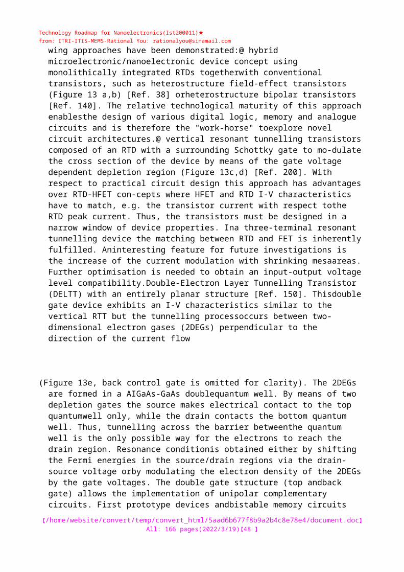
Technology Roadmap for Nanoelectronics(Ist200011)★from: ITRI-ITIS-MEMS-: [email protected]
general a nuisance for the practical applications, particularly because the freespace impedance is 377 Ohm and typical strip line or coplanar waveguide have characteristic impedancebelow this value. For an interference effect with an electronic waveguide at high (microwave) frequencieswithout extensive loss, a built-in amplifier or a switch with a negative differential conductance, such asfound in resonant tunnel diodes, is required.Two ID electron systems may couple to each other in several ways where the broad band transmissionthrough the waveguides is narrowed down by coupling via two coupling contacts along the ID channelsforming an artificial atom (quantum dot) with a discrete energy spectrum. This is similar to the couplingvia a cavity in traditional microwave techniques. The resonant coupling at a ID-OD-ID electron systemhas shown to exhibit negative differential conductance [Ref. 195]. Although the peak-to-valley ratio is low,it this may be the basis for making resonant tunnelling transistors for future circuits. Therefore, TexasInstruments is also investigating the possibility to produce resonant tunnelling transistors operating with aplanar lay-out [Ref. 30,181].
3.6.4. Double electron waveguide device A finely tuned pair of parallel electron waveguides has been proposed for analogue to digital (A/D)
con-version. The device consists of two electron waveguides in parallel configuration and is called a DoubleElectron Waveguide (DEW). The operational concept of this device is based on the phenomenon of
ballistic transport in electron waveguides that results in a staircase conductance G(V@) of the waveguide asfunction of a gate voltage (V@) that changes its width. In a DEW, the G(Vp.)s of the two waveguides areappropriately shifted to obtain a regular, square-wave output conductance otthe device [Ref. 50] as func-tion of a gate voltage. Such an output can conceivably be used in a parallel architecture to generate a direct,binary A/D conversion, requiring only N DEW devices for N-bit conversion. Since transport is ballistic,power consumption of a DEW is very small, of the order of a Ws. Also, since the dielectric response timeis very small, the intrinsic response speed or frequency response of a DEW could be very high (I ps). Theoperating speed will obviously depend on the RC time constant of the device gate circuit. The expectationis that the DEW device concept will lead to potential applications in high-speed (10 GS/s), very low-power(I W) and A/D conversion with high resolution (5 bits).
3.6.5. The 3-terminal (Y-Branch) switching devices "Artificial" atoms can be made by electrostatic confinement of a 2D electron gas in the two lateral
direc-tions. To produce a 3-terminal device, such an "atom" must be coupled to some leads in a waveguide struc-ture. The simplest 3-terminal concept is a confined region with three electronic waveguides leading intoone middle region. Due to it form it is generally called an Y-branch device. Fig. 18 shows a SEM pictureof such a device. The very open structure at the Y-junction permits no Coulomb blockade. The extendedstates in the Y-junction are strongly modified and the transmission from source (see fig. 18) to either leftor right drain is a delicate balance, which depends on the full self-consistent solution in this region. A slightchange of geometry where a bias on the left or right gate may very quickly switch the two drains betweenhigh (2eVh) and low conductance. This switch is a result of an amplified effect of changing the confine-ment; i.e. a small rearrangement of charge on the gate capacitance has due to the wave-mechanics a biginfluence on the transmission in one or both source-drain channels [Ref. 168]. The limitation of this deviceis its intrinsic low working temperature, which is needs that the subband and Fermi energies are larger thanthe thermal energies, i.e. below 50 K.For such a Y-branch device, the mean free path length for ballistic coupling is in the order of 100-200 nmat room temperature. Y-branch devices fulfilling this criterion can be produced so that QPC couplingbetween the
【/tt/file_convert/5aad6b677f8b9a2b4c8e78e4/document.doc】All: 107 pages(2023/5/6)【48 】
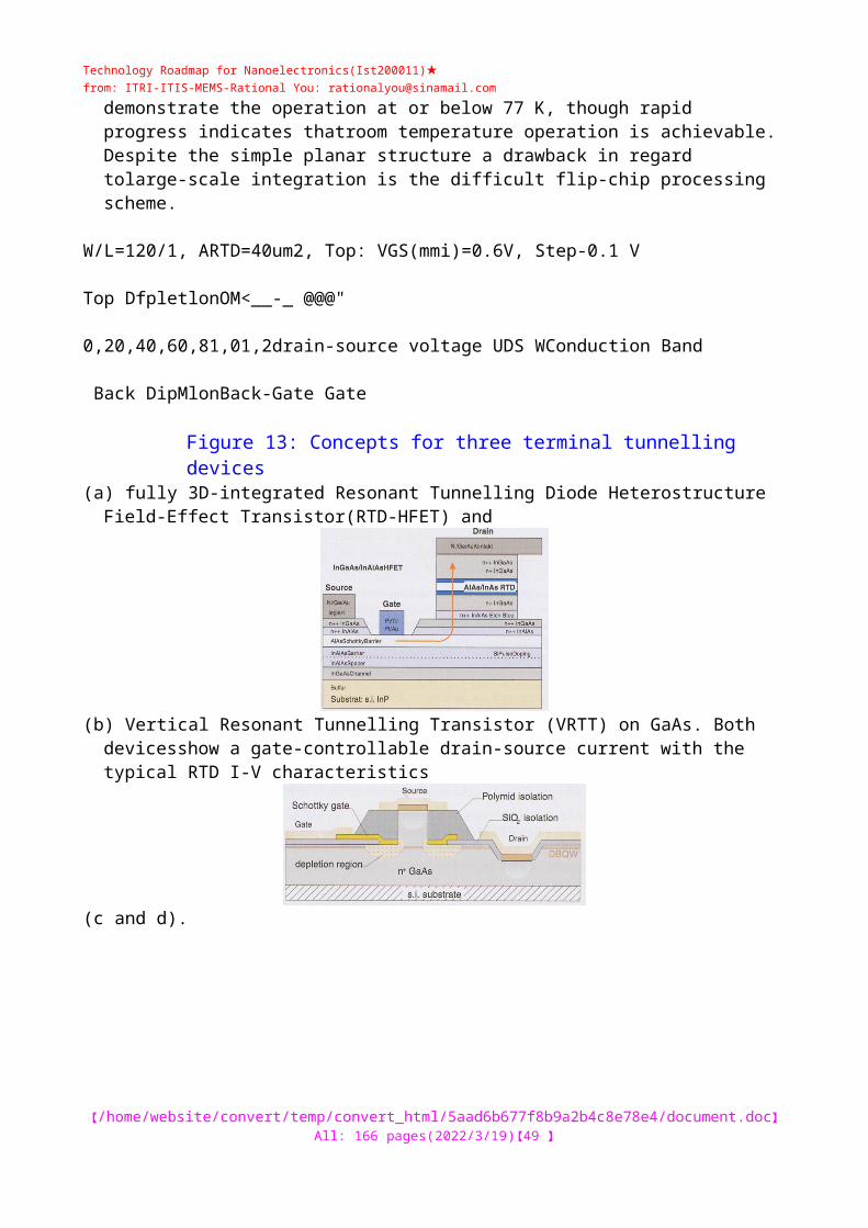
Technology Roadmap for Nanoelectronics(Ist200011)★from: ITRI-ITIS-MEMS-: [email protected]
source-left drain and source - right drain can be observed. The fact that the stem copies themost negative of the voltages applied to the two other electrodes makes it a candidate for rectification upto the THz regime [Ref. 233]. Furthermore, it has been shown [Ref. 234] that such Y-branch devices pro-vide properties suitable for logical circuits. Strictly speaking, this is, however, neither an interference devicenor a waveguide device, since the thermal energy is larger than the typical Fermi or subband energies in theY-junction.
Figure 18: Y-branch Switch
Scanning electron microscope (SEM) picture of a heterostructure defined Y-branch switch. Theetched ridges support a ID electronic waveguide, which carries currents from the upper sourceregion to either of the two lower drain regions. The left or the right gate voltages give rise to anabrupt switching in resistance between the source and the left (or right) drain. The switching isgoverned by large waveguiding changes at the Y branch point and only indirectly due to charg-ing effects. [Ref. 233]
【/tt/file_convert/5aad6b677f8b9a2b4c8e78e4/document.doc】All: 107 pages(2023/5/6)【49 】
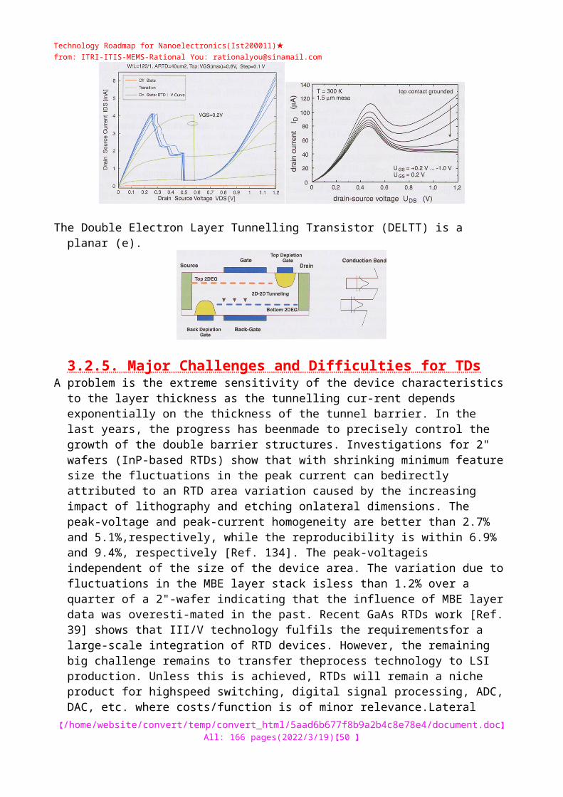
Technology Roadmap for Nanoelectronics(Ist200011)★from: ITRI-ITIS-MEMS-: [email protected]
'{'echnolo@y Roadmnf} for Nilnoelectroillcs
3.6:6. Major challenges and difficulties for electron interference and switching devices
A. Fabrication tolerances and temperature limits Quantum mechanical interference driven by a gate voltage or a magnetic field requires that the states that are responsible for the interference have a coherence length that is longer than the region over which the coherence occurs. In order to have a simple type of interference the geometry must be simple with a small number of unintended electron scattering points in the sample. The interference effect will be destroyed once the thermal energy becomes comparable to the lowest ener- gy differences in the system causing the interference. In an ideal ID-system it is the subband energy dif- ference that sets the limit. For a ID waveguide with a confinement corresponding to a subband separation energy of 1-10 meV, the maximum temperature will then be 5-50 K. To reach room temperature the device sizes must be smaller than 10 nm [Ref. 122].B. High frequency limitationsThe interest in coherence phenomena and switching is particularly pointing towards high frequency usageup to THz. The existence of a minimum resistance of ID devices, given by the resistance quantisation valueh/2e'=12.9 kOhm is however an intrinsic problem. This resistance will always appear in series with themodulated value. The strong impedance mismatch between 12.9 kOhm and the typical transmission lineimpedance of 50-400 Ohm will lead to a considerable loss of signal unless special measures are taken tomatch impedances. The obvious way is to work with waveguide devices with a built-in amplification(switching devices) or by having an amplifier (HEMT) closely integrated in the designed waveguide circuitlimiting the frequency response to about 0.1 THz. The impedance problem will be a major challenge forany nm circuit that may become relevant for high frequencies in the future.C. Periodic versus on-off devicesThe interference phenomena discussed above comes about as a quantum mechanical phase shift betweentwo partial waves giving a periodic, often sinusoidal, variation of the conductance with the externallyapplied magnetic or electrical fields. The periodic response leads to the same conductance for several dif-ferent external field values; this is generally not desired and preferentially there should be a one to one cor-respondence between input and output. Most application will require a digital signal handling and theswitching devices mentioned above may therefore be most suitable.
【/tt/file_convert/5aad6b677f8b9a2b4c8e78e4/document.doc】All: 107 pages(2023/5/6)【50 】
Technology Roadmap for Nanoelectronics(Ist200011)★from: ITRI-ITIS-MEMS-: [email protected]
4. Nanofabrication
As discussed in section 2 on MOSFETs, optical lithography has been a key element in the success ofCMOS technology. Year upon year the required performance on critical feature sizes has been achievedusing smaller wavelengths. In addition using top surface imaging, silylation of resists, sophisticated masktechnology including phase-shift masks and optical proximity corrections, has pushed the physical limitsfurther down. It is believed that optical lithography might be used for the 100 nm technology node. Thisimplies more complex masks and processes and costs for this type of sophisticated equipment are very high."Next Generation Lithography" options are currently being investigated and include extreme ultraviolet(EUV), X-ray, projection electron-beam and projection ion-beam lithographies.There are a number of ways to create small structures. Many technologies are based on replica generationemploying some kind of mask, similar to conventional optical lithography, but a number of novel tech-nologies leave out the mask as an intermediate step. ITRS specifies that the minimum feature sizes forCMOS technology is rapidly moving to the nanoscale regime (see Table 1). In particular the 100 nm tech-nology will be introduced in the year 2005, 70 nm in 2008, 50 nm in 2011 and 35 nm in 2014.Investigation is under way to have appropriate equipment for the corresponding timeframe.Industrially applicable nanofabrication techniques must comply with the driving requirement to producemillions or billions of small structures in a quick, reliable and cost-effective way. In addition, suitable tech-niques must be able to connect these structures in a predefined manner. For this reason, parallel techniques,such as conventional optical lithography employing mask alignment and pattern transfer seem to be theonly economically viable way towards highly integrated circuits. Serial techniques, such as scanning probetechniques or single electron beam lithography, may be employed for fabricating masks or single compo-nents, but do not offer adequate throughput for large-scale integrated circuits.
Table 7: Maturity of Lithography OptionsFor each exposure tool, the table indicates the time when it is expected to be an
industriallyacceptable option.Year of
Introduction2001 2003 2006 2009
Minimum feature size (nm)
150 120 90 65
Overlay (nm) 55 45 35 25Optical 193 nm @ @Optical 157 nm @ @Extreme
Ultraviolet@ @
X-rays @Electron beam @ @Ion beam @ @Printing @
Table 8: Practical and Ultimate Resolution Limits for LithographyFirst, a brief review on optical and "next generation" lithography methods currently investigated for
CMOStechnology will be presented. The pros and cons are widely discussed in industrial forums and a time sche-
Lithography Type
【/tt/file_convert/5aad6b677f8b9a2b4c8e78e4/document.doc】All: 107 pages(2023/5/6)【51 】
Technology Roadmap for Nanoelectronics(Ist200011)★from: ITRI-ITIS-MEMS-: [email protected]
Practical LimitUltimate LimitUltraviolet lightContact / proximity2500 rimFresnel diffraction at minimumpracticable gap and wavelength.Wavelength 200 nm, gap
25 jim125 nmFresnel diffraction for contact printwith 100 nm thick resist. Wavelength160nm, gap 100
nm______________50 nmUltraviolet lightProjection150 nmFraunhofer diffraction at NA setby fabrication and field-sizelimits with phase shift mask
etc.Wavelength 157 nm, NA 0.75,depth of focus 0.3 u.m_________Fraunhofer diffraction at wavelengthset by transparency of resist andoptical materials.Wavelength
157nm,NA0.9,depthof focus 0.2 am. field size <200u,mExtreme Ultravioletprojection(Soft X-rayprojection)90 nmFraunhofer diffraction at NA setby achievable tolerances onoptical components.Wavelength
13-15 nm, NAO.I,depth of focus 1.4 urn30 nmFraunhofer diffraction and resistresolution limit.Wavelength 13 nm, NA 0.3, depth offocus
0.07 p.m.X-ray proximity70 nmAbsorber aspect ratio andFresnel diffraction at practicablegap for step and
repeatoperation.Wavelength I nm. gap 5 urn10 nmFresnel diffraction for contact printand resist resolution limit.Wavelength I nm, gap 100 nmIon beam30-50 nmion optical limits (chromaticaberration) and interaction rangewith resistResist; 10-20nmDelocalisation of exposure(secondary electrons) and ion opticallimits (chromatic
aberration)Ion milling: 10 nmDelocalisation of sputtering processElectron beam(low energy beamarrays)40-50 nmLateral scattering of electrons inresist and/or interaction range ofexposure process.Resist: 7 - 20 urnDelocalisation of exposure(secondary electrons)Direct exposure / sublimation: 1 -
5 nmCombination of electron interactionrange and electron optical limits(diffraction and spherical aberration)
Electron beam(Scapel)90nmresist sensitivity35 nmelectron - electron interactionImprinting20-40 nmMaterial reflow, distortion offeatures under the stresses oftemperature and
pressure,alignment of structures for chipat once.8-10 nmradius of gyration of the polymerInking30-50 nmSurface diffusion of molecularinks, structure-propertyrelationships of
elastomericmaterials.10 nmradius of gyration of high molecularweight (polymeric) inks.Scanning ProbesMethods(STM / AFM)0.5 nmAtomic resolution
dule when the maturity level for industrial application is achieved is given in Table 7. If they will be sui-table for nanofabrication does not depend upon their throughput, but solely upon the
【/tt/file_convert/5aad6b677f8b9a2b4c8e78e4/document.doc】All: 107 pages(2023/5/6)【52 】

Technology Roadmap for Nanoelectronics(Ist200011)★from: ITRI-ITIS-MEMS-: [email protected]
resolution limits.The resolution limit for exposure tools is summarised in Table 8, making a clear distinction between theunderlying physical limits and those due to practical and production considerations. Then an emergingalternative for nanofabrication will be presented, that will be hopefully ripe for future device generations.Generally speaking, these can be divided into top-down methods, where small structures are fabricated bydeposition followed by lithographic patterning and etching, and bottom-up methods where fabricationstarts at the basic molecular or single device level and assembles circuits by pulling devices together,
4.1. Lithography for CMOS technology
Table 7 lists potential lithography solutions to be used in the next decade for CMOS technology.
4.1.1. Optical lithography Currently optical lithography is the dominant exposure tool. Using projection optics, the resolution
variesas (kiX,)/(NA) where k@ is an empirical process parameter, X. the source wavelength and NA the numeri-cal aperture of the optical system. The depth of focus varies as (k@)/(NA)2 . The decrease of the criticaldimension is based on using light with a shorter wavelength, successively using mercury G-line (436 nm),mercury 1-line (365 nm), followed by excimer lasers, in particular KrF (248 nm) for the 180 nm genera-tion, ArF for 197 nm and F2 for 157 nm.Development efforts are focused towards optical materials that allow aberration free lenses with large va-lues of NA in addition to resolution enhancement techniques to yield smaller values of k) and k@. Theyinclude off-axis illumination, attenuated and alternating phase-shifting masks, optical proximity corre-ctions, and top surface imaging techniques. The use of optical proximity correction (OPC) and phase-shif-ting in mask technology requires structures with lateral dimensions four times smaller than the criticaldimension.
The drawback is a worse mask definition and a reduced focus depth, which requires a thick-ness control and reduces manufacturing process window. It appears physically feasible to achive opticallithography with sub 100 nm resolution. Many technological hurdles such as the mask fabrication and itsrepair, the availability of sensitive high resolution resists or overlay problems remain to be solved.
4.1.2. Extreme Ultraviolet lithography Extreme Ultra Violet (EUV) lithography or soft-X-ray lithography is the natural successor of
convention-al optical lithography on its way towards smaller wavelengths [Ref. 81]. Major differences are the need for reflection optics and masks at wavelengths in the range 10 to 15 nm, using multilayer mirrors. 100 nmline-and-space and 70 nm isolated lines have already been demonstrated. EUV lithography is supposed to be introduced, if mature for production, at 90 nm. The method is attractive for CMOS as it holds thepromise to be extended down to 40 nm, but has a long way to go before being introduced into produc- tion.The EUV source must offer high power, with synchrotron radiation and plasma laser sources as possiblealternatives. On the one hand synchrotron radiation is a mature technology and provides the necessarytechnical solutions, but it is not popular in industrial environments, as semiconductor fabs have to be builtaround expensive synchroton facilities. On the other hand laser plasma sources providing high power with-out debris would be a cheaper solution but they are not mature yet. Any EUV exposure tool involves mul- tilayer collectors and mirrors. Providing the reduction factor and the specifications for these optics is verytough. In particular, the surface and interface roughness of the mirrors and collectors has to be better than 0.25 nm. In addition the multilayers must be stressless and robust to thermal effects. In compensation, thevery low value of the numerical
【/tt/file_convert/5aad6b677f8b9a2b4c8e78e4/document.doc】All: 107 pages(2023/5/6)【53 】
Technology Roadmap for Nanoelectronics(Ist200011)★from: ITRI-ITIS-MEMS-: [email protected]
aperture of the EUV system allows for better depth of field than in con-ventional optical lithography. Mini-steppers have been realised. Similar to the mirrors, the mask also must be reflective. Generally it is produced by depositing a metal on a multilayer (typically Mo/Si) and subsequent patterning. A posteriori repairing of the multilayer is not fea- sible, and a careful control of defects during growth is therefore essential.
4.1.3. X-ray proximity lithography X-ray proximity lithography [Ref. 197], using a typical wavelength of I nm, represents the last step
in the decrease of photon wavelength for nanolithography purposes. It has been intensively developed by acade-
mia and industry during the past 18 years, and is nearly ready for use. In the absence of appropriate X-ray optics, it is based on a direct I: I wafer imaging behind a mask. In order to offer sufficient throughput, theX-ray source is either synchrotron radiation or a plasma laser source. The former is commercially available and has a very low downtime per year, while the latter is under development. Commercial steppers are available, even if they need further improvements for future generations. The mask technology has made good progress: an X-ray mask consists of relatively thick (a few hundred nm) high atomic number mate- rial structure, on a large area 1000 nm thick SiC membrane. Stress control of these masks, essential for pat- tern placement accuracy, is not a problem. Zero defect masks have been demonstrated. Additional advan- tages of X-ray lithography are the easy single layer resist process and high reproducibility. A number of integrated circuits or device demonstrations have been produced with dimensions not yet reached by com-peting methods.The largest disadvantage are the huge costs. Further drawbacks are the lack of an electron-beam patterngenerator with a suitable throughput for writing the I: I mask, the stability of the masks after the highnumber of irradiations required to make the method cost-competitive, and a full demonstration ofextendibilily to 70 nm ground rules.
4.1.4. E-beam projection lithography and Scalpel Electron beam lithography (e-beam) makes use of the fact that electrons can be deflected and
modulatedby electrostatic or magnetic fields to produce an image. The fundamental resolution limit is given by theHeisenberg uncertainty (Ax Ap >h/27t) offering the possibility to achieve patterning below 10 nm (for elec-trons in the eV to keV region the resolution can be expressed by the following expression:Ax I/E'" , being E in eV and x in nm). There are two ways to perform e- beam lithography, either by scan-ning the beam to generate patterns or to perform electron imaging through masks.Current e-beam lithography systems are mainly serial technologies, which are limited by the scanning speedof the e-beam in the pattern generation. The throughput may be increased by a matrix of parallel e-bearns.This increases the complexity of the system and puts high requirements for the individual beams in termsof brightness, energy spread and beam opening, as well as on the optics of the lenses. For example, newsources must be developed that allow array emission. On one side, Spindt type field effect arrays offer thepossibility in the low voltage regime (less than 250 eV at currents smaller that 500 A), but the current fluc-tuations from the tips cause constantly changing field emissions that can not be tolerated. On the otherside, micro-fabricated Si tips offer good control of the tip location and would provide the possibility of anactive matrix, but the surface state of the emission area is difficult to control having effects on the fieldemission uniformity. An additional approach is to use carbon surfaces (diamond like carbon or nanotubes)for electron emission. Ideally, any appropriate source must be robust and able to operate at hard environ-ment conditions, i.e. insensitive to the degassing from non-clean wafers and intrinsic to the fabricationprocess (resin deposition, chemical bath treatments), a good brightness, a low energy spread and operatesat a
【/tt/file_convert/5aad6b677f8b9a2b4c8e78e4/document.doc】All: 107 pages(2023/5/6)【54 】
Technology Roadmap for Nanoelectronics(Ist200011)★from: ITRI-ITIS-MEMS-: [email protected]
low energy.High energy electrons have the effect to damage samples and to destroy the gate structures by the dissipa-tion of the build up charges. One of way to circumvent this problem is to use low energy electrons thathave a low penetration depth. In particular e-beams with an energy below 300 eV (mean free path < I nm)are supposed not to charge the sample nor to contaminate the surface.To achieve arrayed focused e-beams two main ways are currently investigated: microcolumns and micro-guns. A microcolumn consists of a non-planar technology construction of about 4 mm in height inclu-ding a Schottky tip as e-source, a filter and a set of microfabricated lenses and detectors. In the alternativemicrogun concept, the electrodes, the deflectors and the detectors are micro-fabricated planar on a Si wafer.For the microcolumn (V= lkV) approach, Chang (Etec 1999) estimates the required performance of thesystem fora 100 nm lithography with a pixel spacing of 50 nm in the following way: For a throughput of10 wafers (300 mm) per hour, the system requires 50 columns operating at 30 nA per column or alterna-tively 200 columns at 0.8 nA per column. If the throughput should be increased to 25 wafers / hour theall numbers would scale with the factor 2.5 and so on. In view that the limiting factor is to offer high expo-sure per area, the tendency in both techniques, microcolumns and microguns, is to increase the number ofarray elements while keeping a high current per beam. In particular, there are to major bottlenecks. First,to produce a stable and reliable sources which work at low energy, high coherence, etc and that are reliable
to work in an array structure under fabrication environment. Second to develop a microfabrication tech-nology to produce lenses, detectors in a precise and economically effective way.Current research efforts are aimed to optimise array e-beam projection systems that would be applicablebelow 100 nm lithography. Measurements with single electron beam at low energy (< 300 eV) indicate thatresolutions of 30 nm are feasible with a single spot. In the long term, a resolution in the order of 40-50nm could be the practical limit of an array system with an industrially adequate throughput.The scattering with angular limitation projection electron-beam lithography (SCALPEL) approach com-bines the high resolution and wide process latitude inherent in electron beam lithography with thethroughput of a parallel projection system [Ref. 91]. In the SCALPEL system, a mask consisting of a lowatomic number membrane and a high atomic number pattern layer are uniformly illuminated with high-energy electrons (100 keV). The entire mask structure is essentially transparent to the electron beam, sovery little of the beam energy is deposited in it. The portions of the beam, which pass through the highatomic number pattern layer, are scattered through angles of a few milliradians. An aperture in the backfocal plane of the electron projection imaging lenses stops the scattered electrons and produces a high con-trast image in the plane of the semiconductor wafer.In contrast to other approaches to electron or ion beam projection where stencil masks are used, the maskfor SCALPEL consists of a continuous layer. This way even doughnut like structures, which are unavai-lable in stencil masks, can be realised. The thin membrane (S@N@ ) is supported by a grid of struts, thatstabilise the membrane and at the same time serve as heat sinks, minimising thermal stress during expo-sure. The lithography is a 4:1 projection. So the mask structures fora 100 nm process are in the 400 nmrange, which allows a fabrication by standard tools for optical lithography masks. Down to 100 nm featuresize no proximity correction is necessary, so the mask design is an easy 4:1 copy process from the features to be produced.As a 'die at once' exposure requires strutless masks and large field electron projection, with extensive and expensive correction systems, the SCALPEL approach uses a step and scan strategy. Between the struts of the mask the pattern is present in stripes. The electron beam shape is a square of 1x1 mrn@ The pattern stripes are mechanically scanned through the beam and the wafer stage moves synchronously. Errors are detected by an interferometer and fed into a stitching deflector which can correct them at nanometer size. The trade off between high throughput and slow mechanics
【/tt/file_convert/5aad6b677f8b9a2b4c8e78e4/document.doc】All: 107 pages(2023/5/6)【55 】

Technology Roadmap for Nanoelectronics(Ist200011)★from: ITRI-ITIS-MEMS-: [email protected]
leads to an additional electronic scanning of the beam on mask, allowing for an effective size of 3 mm@ for the projected field on the wafer (0.25x0.25 mm@ without scanning). Several series of marks are used for wafer alignment, die alignment and stitching alignment, allowing for a high overlay accuracy. One limitation is the throughput, which strongly depends on the beam current and the resist sensitivity. A sensitivity of 10 pC/cm@ allows for a throughput of 1.5 x 8-wafers per pA beam current. The interaction of the electrons inside the beam lead to an intrinsic blur, proportional to V" and limits the resolution to about 35 nm at 10 \iA. Improvements can be made by increasing the resist sensitivity. The latter includes an improvement of the stage performance, as the movement of mask and wafer may then be a limiting fac- tor. The resolution is mainly affected by the blur in the beam and projection errors. The sensitivity to dose variation and the depth of focus (mask deformation) is much lower than optical lithography. At present SCALPEL can be expected to deliver accurate lithography results down to less than 100 nm with good line- width at a reasonable throughput if the necessary beam current can be managed and the resist sensitivity can be further reduced.
4.1.5. Ion beam projection Focused electron beams and focused ion beams have been used to write dimensions into resist well
below 20 nm, but because of the serial writing process these techniques are far too slow for high volume produc- tion purposes. Projection systems [Ref. 141], employing a mask and performing parallel printing of whole images, com- bine both high resolution and high throughput. Ions are particularly well suited for this because they suf- fer little or no scattering in a resist (small proximity effect) and the resist sensitivity is high because the range of light ions (H* ; He" ) in the resist in the 50- 100 keV energy domain is typically in the same order
of magnitude as the resist thickness. For chemically amplified standard deep-UV resists which are also use-ful for ion exposure the resist sensitivity is 10" to 10" ions/cm@ (0.16- 1.6 pC /cm@ ), which allows forexposure times of below I second in a 10-100 mm' field.So far with an ion projection lithography (IPL) system 50 nm wide lines have been produced in relativelythick (300 nm) resists at a reduction rate of 8,7 from mask to wafer [Ref. 34]. With thinner resists resolu-tion below 20 nm is expected.Ions can also be used for resistless processes where ions directly modify the surface of a substrate. Interestingapplications are the production of magnetic nanoislands or of quantum dot arrays by damage writing. Theion projection technique will enable the necessary printing speed.For a comparison of writing speed between e-beam and ion exposure it has to be considered that ions ofadequate energy 50-100 keV deposit their energy completely in the resist layer while electrons of 100 keVpenetrate deeply into the substrate. This leads to quite different resist sensitivities (= dose to clear large areasin (iC/cm@). Table 9 gives the sensitivity per type of lithography.
Table 9: Sensitivity perType of LithographyLithographyIon Projectione-beam (Scalpel)Extreme-UVDeep-UV11.3mJ/cm (= 0.15 @C/cmx 75-10 @'V)400 mJ/cm (= 4jLlC/cm@ x 100-10@)10 mJ/ cm'15 mJ/ cm'
Energy that is transferred onto the wafer is calculated by the dose to clear large areas times the【/tt/file_convert/5aad6b677f8b9a2b4c8e78e4/document.doc】
All: 107 pages(2023/5/6)【56 】
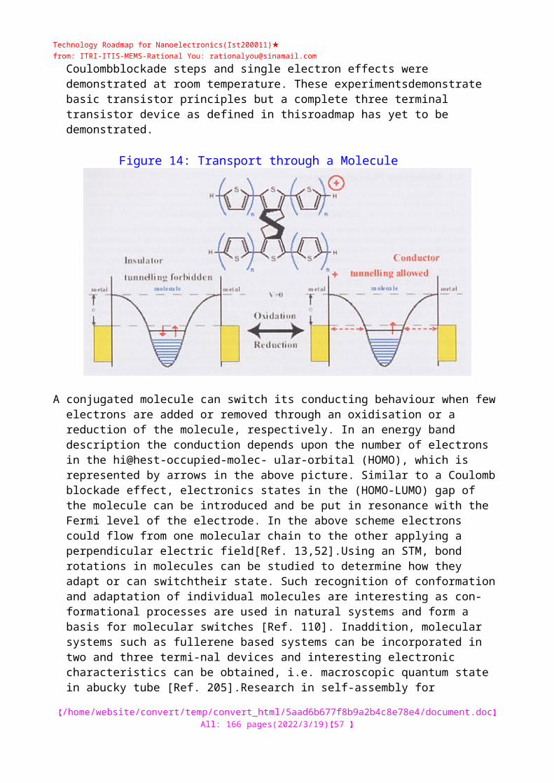
Technology Roadmap for Nanoelectronics(Ist200011)★from: ITRI-ITIS-MEMS-: [email protected]
acceleration voltages of the particles.Note that for an accurate estimation of the throughout numbers, besides sensitivity, other critical factors,such as Coulomb interaction in dense particle beams, have to be taken into account.
4.2. Emerging nanofabrication methods 4.2.1.Electron Beam Nanolithography
Electron-beam lithography is the essential basis of nanostructure fabrication at present. Gaussian beam pat-tern generators or scanning electron microscopes are used with high-energy electrons (100 to 200 keV) anda small electron probe size (I to 10 nm). Using high resolution and low sensitivity PMMA resist, dimen-sions down to 30 nm are routinely produced in many research laboratories with high reproducibility.Resolutions down to 7 nm have been demonstrated. Smaller dimensions have been shown in inorganicresists, but no adaptable transfer method has made them usable. Progress has been made for reproducibi-lity at the nanometer scale: NTT has presented a SET operating at room temperature whose structure hasbeen produced by e-beam lithography. The Si Island is 10 nm thick and the Si tunnel barriers I nm [Ref.124]. Room temperature SETs using Si point contacts fabricated on a SIMOX substrate can be fabricatedwith an electron beam using an anisotropic soft stopping technique that defines the point contact width[Ref. 102].
Table 10: Resolution and Sensitivity for E-beam Lithography
Process ResistSmallestIsolatedfeatures
ResistMinimumcntr
/cntrspacing
Structures
Smallestisolatedfeatures
Structures.Minimumcntr
/cntrspacing
Sensitivity Devicesfabricated
Spin-onResist(PMMA)
7-10 nm 30-50 nm 7 nm 40-50 nm IO@nC/cm@ Yes
VapourResist(contamination)
5-8 nm 40-50 nm 3-8 nm 40-50 nm 10@0/01112 Yes
DirectSublimation(NaCI,
AIP@..)
0.5-2nm 4nm 10 nm 20-30 nm 0.01 - 10mC/cm
No
Direct exposure(SiO@)
3-10 nm 15 nm 5-10 nm 15 nm 2-5mC/cm2 No
Direct exposurehigh T@superconductors
30 nm ? ? 30 nm ? ? >200mC/cm@ Yes
The biggest disadvantage of all this technology is the large writing time, causing a low throughput thatmakes electron beam lithography prohibitively expensive for the mass production of integrated circuits.Current research is focused on this problem, with the following approaches:@ parallel exposure, and the SCALPEL method described above, is a promising approach, getting closer to
a realistic throughput, but its resolution capability is not yet known.@ very low energy e-beam writing: due to the increase of resist sensitivity, the throughput can be increased
by a number of orders of magnitude. The low energy electron-beam writing has not yet
【/tt/file_convert/5aad6b677f8b9a2b4c8e78e4/document.doc】All: 107 pages(2023/5/6)【57 】

Technology Roadmap for Nanoelectronics(Ist200011)★from: ITRI-ITIS-MEMS-: [email protected]
demonstratedresolution below 50 nm,@ parallel writing using arrays of microfabricated microcolumns.@ more
sensitive resists, such as chemically amplified resists, for which the effort concerns process window
and resolution limits, and in the optimisation of the electron beam process and the development of more
sensitive resists,The present resolution, sensitivity, and applications of electron beam nanolithography are summarised inTable 104.2.2. Scanning Probe MethodsThere is a steady progress developing Si-based devices using scanning probe methods. Resolution seems notto be a major concern, but for any application in fabrication, throughput becomes an important issue.Efforts in employing large arrays of scanning probes are certainly promising, with arrays of up 50 SPMshaving been fabricated [Ref. 146], but it remains to be seen ifSPM can ever intrinsically surpass parallellithographic methods.4.2.3.PrintingThere are two main strands to nanometer-scale printing. The first one relies on the moulding of a thinpolymer layer by a stamp under controlled temperature and pressure and will be referred to as imprinting
(also called hot embossing or nanoimprint). The second one is based on the transfer of a monolayer of self-assembled molecules from an elastomeric stamp to a substrate and will be referred to as inking. Both tech-niques obey to the need to develop a competitive parallel process, in terms of reliability, throughput andcosts. In the following the basic principles, bottlenecks and prospects of imprint and inking will be dis-cussed and compared. Variations of these main strands as well as the status of combined nanofabricationmethods will be discussed.
4.2.3.1. ImprintFigure 19 shows the scheme of the imprint process. After preparation of the stamp by, for example,
opti-cal lithography and or electron beam lithography and dry etching, and the substrate, an appropriate poly-mer-coated substrate, both stamp and substrate are placed on parallel stages. The stages are heated up tothe printing temperature, which is above the glass temperature of the polymer to be moulded, until ther-mal equilibrium is reached. Stamp and substrate are brought into physical contact and pressure is applied,followed by a down-cooling. The heating time and pressure hold time last typically a few minutes each.Demounting and separation of the stamp and substrate takes place when both are at about 50 C. Afterremoval, the resulting polymer relief (thickness contrast) can be used as: (a) a mask for dry etching if theimprinted polymer is resistant enough, (b) a step in a lift off process and (c) assuming the printed polymerhas a functionality (conductivity, optical non-linearity, etc) as a device itself.
Imprint
ReleaseFigure 19: The Imprint Process
【/tt/file_convert/5aad6b677f8b9a2b4c8e78e4/document.doc】All: 107 pages(2023/5/6)【58 】

Technology Roadmap for Nanoelectronics(Ist200011)★from: ITRI-ITIS-MEMS-: [email protected]
Further Processing
There are several key issues that have to be considered if imprint lithography will make it as a competitivetechnology. The major two critical issues are alignment and throughput:A proper alignment is a must for multilevel processes as required in nanoelectronics industry. In firstapproximation, the alignment depends on the stamp size, the thermal and mechanical stability of the poly-mer during alignment and the choice of stamp and substrate material. Imprint lithography must offer asolution for x-y in-plane alignment suitable at least for VLSI application, i.e. better than 10 nm. Forimprint technology, where the stamp is the functional equivalent to the photo-mask in conventional pro-jection lithography, a stepper can be used for the manufacturing process [Ref. 82]. Using an in-house deve-loped printing machine with a commercially available aligner and matching the thermal expansion coeffi-cients of stamp and substrate, alignment to just under I p.m over a 4" wafer has been demonstrated printinggratings with 100 nm features [Ref. 241]. The alignment is given by the limits of commercially availablesteppers that is in the order of I p.m. Alternative optical alignment techniques would also be limited toabout I [im. Recent investigation look for an alignment systems suitable for printing with UV-curing, com-bining an adaptive wafer (substrate) holder with optical detection of diffraction fringes [Ref. 228]. A muchbetter alignment would be achieved with piezo-driven techniques, but this option is applicable only forsmall stamps not bigger than a few mm. It is estimated that, counter balancing thermal and bending effects,piezo-driven approaches could provide an alignment of about 30 nm over 50 mm.
The second key aspect is throughput. A definition of throughput as understood in optical lithography ismissing. An analogue approximation would consider the actual printing or inking time, (ranking from afew seconds to a few minutes), the alignment time (some 10s of minutes), the time required for stampcleaning and replacing and, if needed, the coating with an anti-sticking layer after a number of prints. Forexample, to print a 6" wafer (182 cm') with a pattern of 50 nnn requires about 20 minutes including align-ment and heating and cooling cycles [Ref. 95], resulting at an "exposure rate" of 0.152 cmVs (Fig 21). Inorder to increase the throughput the following measures could be taken:@ Increase stamp size. The stamp size defines the area that can be printed each time. Ideally the stamp wouldhave a size compatible with standard production and process handling. A potential problem is the pa-rallelity of the wafer given thermal gradients in printing, but a suitably designed printing machine mayovercome this hurdle.
【/tt/file_convert/5aad6b677f8b9a2b4c8e78e4/document.doc】All: 107 pages(2023/5/6)【59 】
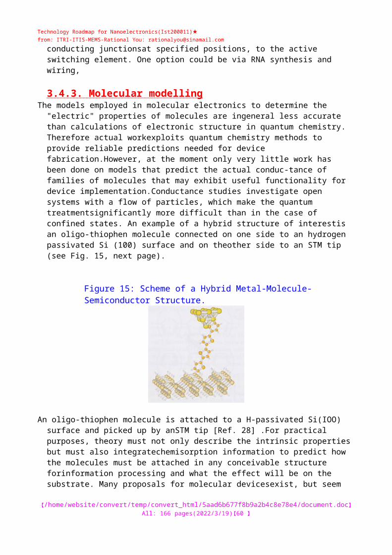
Technology Roadmap for Nanoelectronics(Ist200011)★from: ITRI-ITIS-MEMS-: [email protected]
At present, 6" wafers having representative areas with feature sizes down to 50 nm,separated by several 100s ofnm from the next feature have been printed with a compact disc-like pro-duction setting [Ref. 95]. An alternative step and flash imprint lithography [Ref. 194] has been testedwith 2" diameter stamps and a test-bed machine for 8"diameter wafers is under construction.@ High density of features in a single stamp. Some applications require high density features and the prin-ting is limited by the flow of the displaced polymer. Precise design rules for negative and positive featurespermitting to design large and small features for a stamp would be an asset. To date, in the best case 30nm features are separated by 150 nm spacing covering an area of several mm@ [Ref. 240]. Similar, withthe step-and-stamp variation (36 consecutive stamps) an area of 150 mm@, with features of 400 nm, wasseparated by 400 nm spaces [Ref. 82].@ Absence of an anti-sticking layer during the printing process. The challenge is to find polymers and todefine processing windows that get rid of an anti-sticking layer. The key factors are the printing tempe-rature, the visco-elastic properties of the polymer and the interfacial energy between polymer / substrateand between polymer / stamp.@ Reduction of the polymer curing time. Unless it can be combined with another nanofabrication step,which compensates for the extra time, the aim is to move away from the curing step, through an ade-quate temperature or UV illumination. This adequacy could result from the right use of bi- or tri-layersof polymers with different printing and curing properties. Similarly, the lowering of the print tempera-ture and pressure would permit shorter printing cycles. Current research, have resulted in more per-forming polymers which are already commercially available [Ref. 145].@ Expanding the stamp lifetime. This issue has hardly been explored in laboratory environments, but willbe crucial in for manufacturing. Here, one cost effective option could be to replicate stamps also byprinting. This approach seems feasible as stamps with 400 nm features can be produced by a thermoset-ting polymer in its pre-polymer state and subsequently followed by thermal cross-linking process.Further issues affecting printing technologies are validation and standards. Validation, as a measure forquality control, needs agreement on what are the allowable tolerances for a good print, but there appearsto be a lack of fast quality control methods for printing, but optical diffraction techniques may be suitablefor tool for the monitoring the quality of periodic structures. On the other side standards depend upondesign rules and it is looks premature to define suitable terms.
4.2.3.2 InkingThe inking process can be described as follows (Figure 20): a stamp consisting of an elastometer is
coveredby an ink, which forms a self-assembled monolayer (SAM) after getting in contact with the substrate. Thismonolayer then serves as a mask for further processing either by etching or surface reaction. The latter isparticularly attractive since functionalisation is intrinsic to the inking process.
Release
Figure 20: The Inking Process
【/tt/file_convert/5aad6b677f8b9a2b4c8e78e4/document.doc】All: 107 pages(2023/5/6)【60 】
Technology Roadmap for Nanoelectronics(Ist200011)★from: ITRI-ITIS-MEMS-: [email protected]
Further Processing
Some of the technological challenges for the application of inking are, on the alignment and diffusion ofthe SAM and as well as the deformation of the elastomeric stamp, which is normally made of polydi-methylsiloxane (PDMS).Alignment / multilevel. Mechanical stresses introduced in the PDMS stamp by handling, gravity or forcesgenerated on the stamp/substrate interface during the propagation of the contact front affect negatively thealignment. Furthermore, due to large thermal expansion in the elastomer (for PDMS this is of the orderof 10" I/K), already small thermal fluctuations in the environment makes it difficult to control the effec-tive stamp dimension. A solution is to put a very thin pattern film (< 10 pm thick PDMS) on a rigid car-rier (Si-layer) that reduces the distortion effects acting on the stamp.Diffusion of the ink occurs during the printing stage, i.e. the period of actual contact between stamp andsurface. Diffusion phenomena constitute a complex interplay between gas diffusion, movement ofphysisorbed ink and lateral movement of chemisorbed ink, A reduced diffusion leads to better resolutionand hence to smaller printed feature sizes. The straightforward approach is printing with heavy inks.Simple, long-chain thiols can be extended only to a certain extent (C@Q) since further elongation leads toless-ordered, and thus less etch-resistant monolayers. Research is currently underway to print with otherink types such as multipode thioether adsorbates which do give well-ordered and etch-resistant monolay-ers, while providing less diffusion owing to much larger molecular weights [Ref. 131]. However, as diffu-sion is the mechanism controlling the formation of a protective layer, a reduction of the diffusion wouldmake it more difficult to construct a well ordered pinhole-free protective layer. With thiols, resolution isbelieved to be limited to about 100 nm.In analogy to the previous calculation for printing, the throughput for inking would take into accountactual inking time, the alignment time, the time required for stamp cleaning and replacing and, if needed,the coating with an anti-sticking layer after a number of prints. To ink a 4x4 cm' stamp on a substratetakes a few seconds, say 3. Assuming two minutes for alignment, the total time is 123s giving a "exposurerate" of 0.13 cmVs for a resolution of 100 nm (Fig. 21) As for imprint, similar parameters are relevant forincreasing the throughput:@ Stamp size. In principle, the stamp size is not restricted since the process does not require any pressure,but only a simple contact between stamp and surface. Current stamp sizes are typically in the I cm x Icm range and areas up to 4 cm x 4 cm are currently investigated, using thin elastomeric stamps supportedby rigid carrier [Ref. 188].@ High density of features in each stamp. Feature densities are not restricted. Printing of small and largefeatures
【/tt/file_convert/5aad6b677f8b9a2b4c8e78e4/document.doc】All: 107 pages(2023/5/6)【61 】
Technology Roadmap for Nanoelectronics(Ist200011)★from: ITRI-ITIS-MEMS-: [email protected]
simultaneously is possible and features with a size ratio of 100 have been demonstrated. A mainlimiting factor appears to be the aspect ratio, particularly when printing patterns with large non-contact
areas. In this respect, the use of thin stamps on rigid carrier seems to solve satisfactorily this problem.@ Absence of an anti-sticking layer. While some groups advocate for using an anti-sticking layer on the mas-
ter to facilitate stamp removal, others do not. In any case, if problems are encountered without using
layer, the stamp can be treated with commercially available OTS (octadecyltrichlorosilane).@ Stamp lifetime. Lifetimes and wear of stamps have not been investigated in detail, but good printing
results have been obtained also with several months old stamps and one and the same stamp can be used
for up to 30 times before needing a re-inking [Ref. 100].
4.2.3.3. Comparison of printing techniques and applicationsTable 11 compares inking and imprint fabrication techniques, as well as combined techniques. The
latterseek to capitalise on the flexibility and cost of parallel lithography by using two or more techniques, suchas combining printing with X-ray, UV and electron beam lithography.
inking refers to times without re-inking.Demonstrated applications include diffraction optics, magnetic arrays, biosensors, quantum point con-tacts, single electron transistors, MESFETS and inter-digitised fingers. All these applications benefit fromthe capability to pattern large areas with small features. Furthermore, the use of a specific polymer on agiven substrate may have additional benefits. For example, a polymer suitable for printing in the 10-100nm scale, spun on glass, is at the same time a low-cost biosensor which can de disposed of after one use,thus minimising contamination or, to fabricate a lab-on-a-chip for medical technologies. Here also helpsthe flexibility offered by polymers, which can be made to react to different environments by building che-mical, optical, mechanical or electrical responses.For magnetic arrays, a large area with small features is a holy grail, specially down to 10 nm with as smalla separation as possible. Imprint techniques have been demonstrated to produce dots of 100 nm separatedby 100 nm..
Table II: Comparison of Printing Techniques Data are results of projects Spinup and Nanotech, except (a) [Ref.l94] and (b) [Ref. 43]. (c) for
Processvariation Smallestisolatedfeature(nm)
Pitchcentre tocentrespacing(nm)
Combinedsmallest (S)and largest(L) featuresin a singleprint step
Largestarea printed(L) andAlignment(A)
Imprinttime (T)excludingused&Nooftimes (N)
stampNanoimprintlithography(NIL
)io(b) 30:30 S = 400 nmL =
100 tlmL = 6 " waferA =
1 U,mT = 3 minN= 50
Step andStamp printing 400 800 S = 400 nmL = 300 HITI
L = 150 mnfA = 1 tlm
T = 3 minN= 36
Step and FlashImprintLithography "
40 200 L =2 " wafer t = few secN = 30 @
【/tt/file_convert/5aad6b677f8b9a2b4c8e78e4/document.doc】All: 107 pages(2023/5/6)【62 】
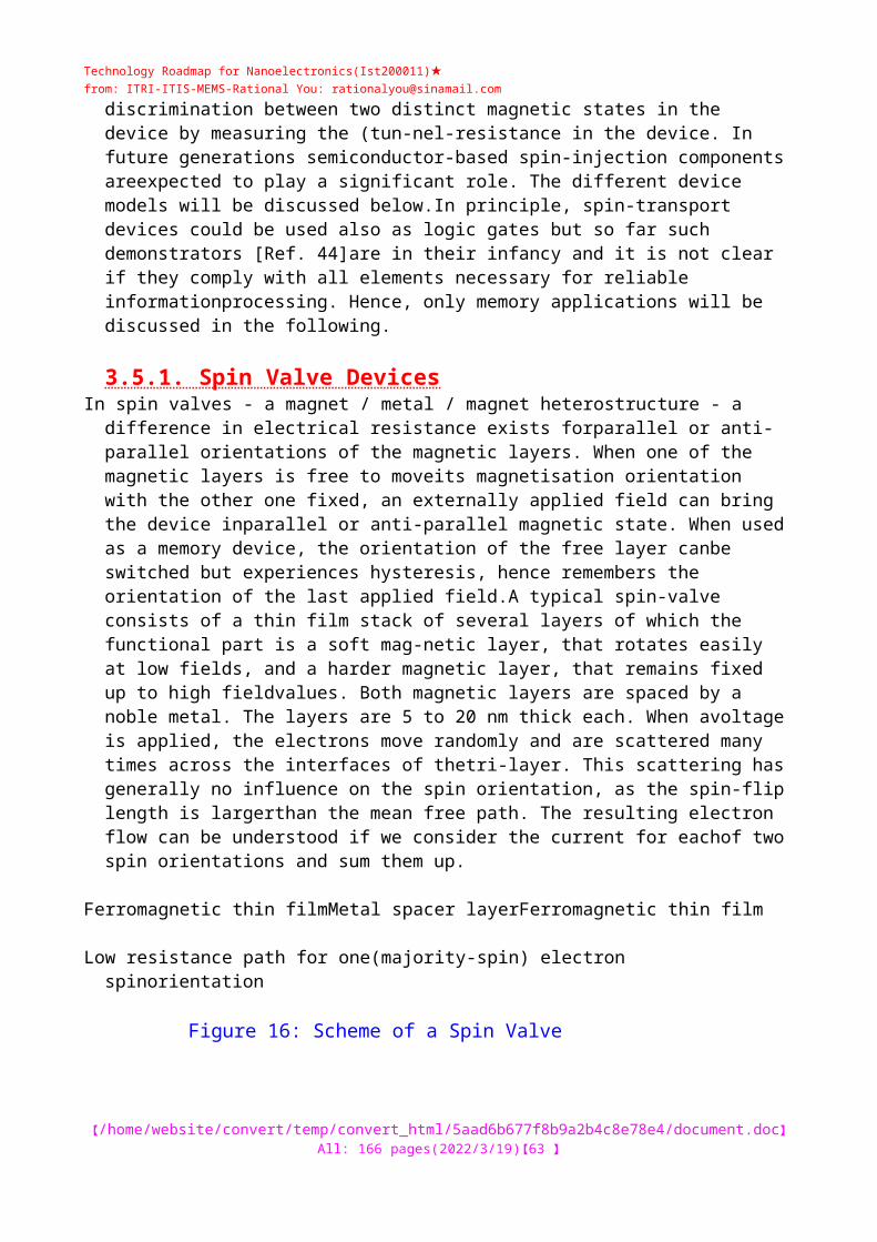
Technology Roadmap for Nanoelectronics(Ist200011)★from: ITRI-ITIS-MEMS-: [email protected]
Micro ContactPrinting 200 100's: 100's S = 2 tlmL -200 flm
L = 4x4 cm
UVLith + NIL 100 200 S = 100 nm L = 400 @m'L = contactpads A = 1 U.m
As printing can be carried out on a polymer spun on a Silicon substrate, followed by standard lift-off tech- niques, this technique can be used for the production of low-cost MSM detectors as the pressure and tem- perature employed in the imprint process is low enough to avoid degradation of the underlying CMOS platform. So far 400 nm inter-digitised fingers have been demonstrated and there is no apparent impedi- ment to go for large areas patterned with 60 nm features for high frequency operation.
4.2.4. Bottom Up Approaches Generally speaking there are two ways to fabricate electronic circuits with nanometer dimensions.
The most frequently used approach employs a variety of sophisticated lithographic and etching techniques in order to pattern a substrate; this is referred to as the top-down approach. The second method is the bot- tom-up approach that builds small structures from the atom, molecule, or single device level upward. This latter method allows in principle a very precise positioning of collections of atoms, hence functionalities. At present, however, the top-down approach has substantially better development than the bottom-up approach. It is fair to assume that for the fabrication of structures with nanometer dimensions, the bottom- up approach will play an essential role in the near future. In order for the bottom-up approach to really become competitive, the following issues are important. Firstly, the classical ways of synthesis, either organic or inorganic, are very cumbersome if well defined, mono-disperse, species of nanosize particles have to be made. A key role is foreseen for self-assembly strate- gies, in which information is present in a limited number of building blocks that allow the spontaneous formation of such well-defined, mono-disperse species. A large number of groups now have methods exploiting non-covalent interactions in self-assembly strategies. The number of strategies, however, that allow the introduction of electronically addressable functionalities is still limited. Secondly, the self-assembled functions have to be positioned in space. Also, here the information should be present in the assembly that allows their own confinement at the desired place. This process could be called self-organisation. The advancement in this respect is less than in self- assembly. An important key is probably played by self-assembly of monolayers on (flat) surfaces and at the same time self-assembly of the various species in this layer. Thirdly, current integrated circuits are highly complex and therefore self-assembly and self-organisation strategies have to be developed that enable the easy formation of complex patterns. The fabrication of pat- terns with nanometer dimensions forms a real challenge for material scientists. Most aspects of assembly and self-organisation, such as positioning of functional groups and their recogni- tion properties, are better developed for organic materials than for inorganic ones, whereas the electronicproperties of the latter are much better understood. It is, therefore, envisaged that especially the combina-tion of the different material types will lead to fruitful new approaches. It may be the case that assembly willtake place via recognition of organic parts followed by derivatisation with inorganic materials, or that smallinorganic units modified with organic anchoring points are assembled into circuits in a single process.In principle, the ultimate dimensions of integrated circuits are defined by the dimensions of atoms andmolecules. At ambient temperature it is probably easier to confine a molecule through its functional groupsthan a single atom. The development of fast methods for performing chemistry
【/tt/file_convert/5aad6b677f8b9a2b4c8e78e4/document.doc】All: 107 pages(2023/5/6)【63 】
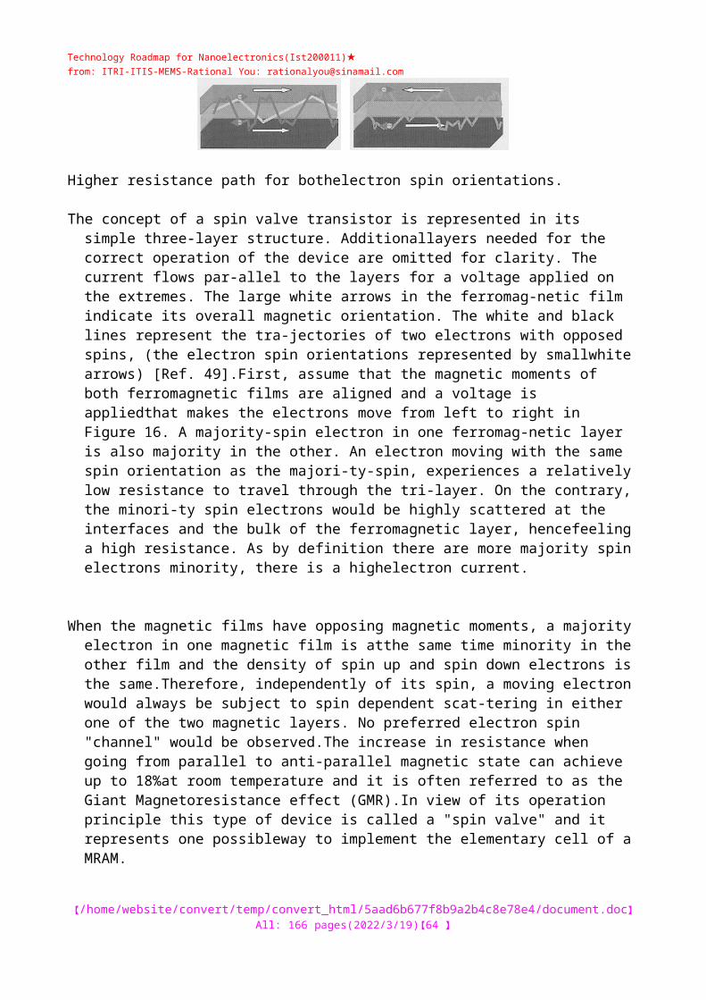
Technology Roadmap for Nanoelectronics(Ist200011)★from: ITRI-ITIS-MEMS-: [email protected]
on single molecules istherefore important. The various probe techniques, like AFM, STM, SNOM, etc. will play a key role inthis field.At the ultimate limits of fabrication, the bottom up molecular and atomic approach is advantageous interms of achievable density and miniaturisation, and the following trends can be observed: at present areview of the literature reveals many designer molecular systems. Much less work is evident on the inter-facing, demonstration of functionality and computation of their behaviour. It is in this crucial area of inter-facing and demonstration of devices that the future progress of molecular nanoelectronics lies. Thereforeself-assembly technologies have become an increasingly popular way of making nanostructures. Manyexamples of self-assembly can be found in the world of organic chemistry, and the ancient technique of fa-bricating Langmuir-Blodgett films has been successfully employed to create structures with specific trans-port behaviour. Moreover, the chemical synthesis of molecules can be viewed as a "self organising" way tomake large numbers of completely identical nanoscale objects. Also in compound inorganic semiconduc-tors, more well-known to the semiconductor world, self assembly is a hot research challenge, especially forthe fabrication of quantum dots.
For all bottom up approaches, it should be realised that for creating useful transport devices, the self-assem-bled structures must be connected to the outside world in a sensible manner. This issue deserves a lot moreattention than so far, as it may be a key impediment for use in commercial applications,
4.3. Comparison of Fabrication Techniques Present day fabrication, as described above, relies almost completely on the top-down approach,
using thehigh throughput optical lithography for dimensions down to 180 nm and electron beam lithography downto 30 nm with a low throughput. Integrated circuit applications needing high throughput such as MPUand DRAM will very probably use optical lithography down to 100 nm. Optical lithography is the pre-fered industrial technique as it is well known and offers high wafer throughput. The future winning expo-sure tool has to offer an adequate compromise between ability to manufacture small feature sizes and a highthroughput. Figure 21 compares these two parameters for a number of exposure techniques. In particularthe exposure rate is a measure for the potential wafer throughput while the minimum feature size is limi-ted by the resolution of the tool [reworked and expanded from Ref. 11].
Figure 21: Throughput us resolution for Different Exposure Techniques
【/tt/file_convert/5aad6b677f8b9a2b4c8e78e4/document.doc】All: 107 pages(2023/5/6)【64 】
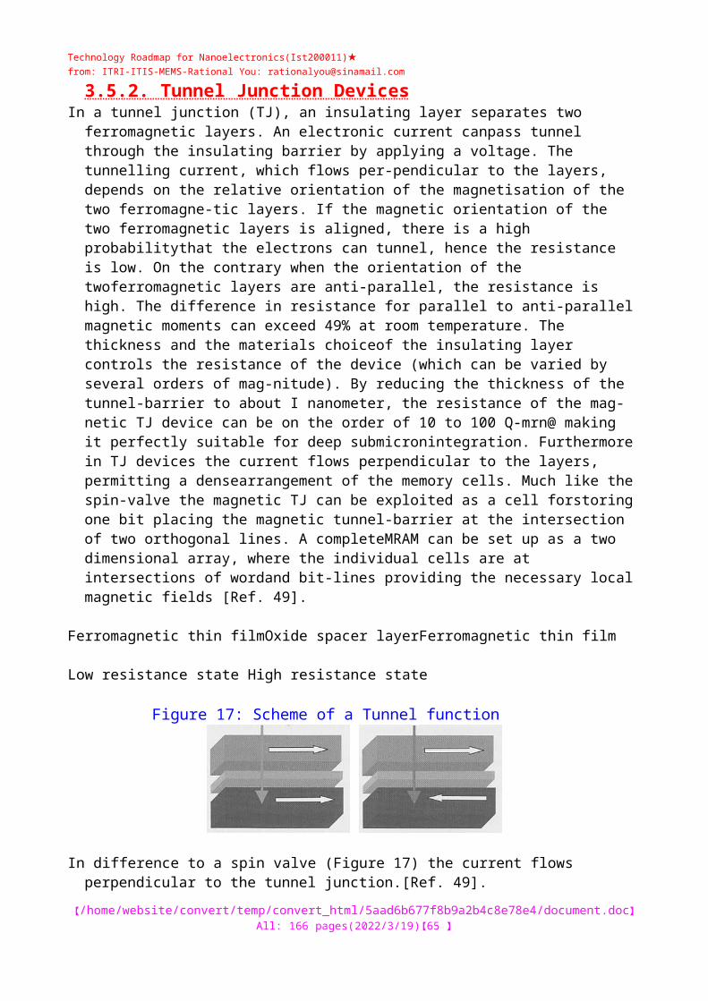
Technology Roadmap for Nanoelectronics(Ist200011)★from: ITRI-ITIS-MEMS-: [email protected]
The situation in the range 100 to 50 nm is more open, and comparison between the extension of opticsand the next generation lithography method is difficult because the development of these methods is high-ly unequal. X-ray lithography and SCALPEL have both demonstrated good results in the literature but asyet still have their own problems which must be solved before it becomes clear which technology will beimplemented below 100 nm feature sizes. Estimation of costs give a small advantage to X-ray compared tooptical lithography at 180 nm, and the difference becomes appreciable at smaller dimension. An essentialpart of this interesting ownership budget is the excellent single resist process given by X-ray lithography,while the process cost of optics becomes high. But optical lithography is an established technology, it hasan easier n:l magnified mask fabrication, and will go on for some generations. A detailed comparison withthe other next generation lithography methods, which are still in the feasibility demonstration stage, is notyet possible. It is still worth investigating all the low cost emerging top down technologies. The introduc-tion of lithography in fabrication might strongly depend on the time of availability of the methods. In addi-tion, whether industry can afford the overall factory costs down to a 50 nm technology is not clear.
It is interesting to note that the dimensions supposed to be reached by these methods (30-50 nrn) coverthe needs of most of the device demonstrations of nanoelectronics (RTD, RSFQ, MRAM). Single electronelectronics is a clear exception, needing controlled dimensions of 1-10 nm. In that case, the bottom-upapproach is the only available solution, coupled to larger structures made by the top-down approach. Itshall be largely the basis of the exploding field of nanotechnology.
【/tt/file_convert/5aad6b677f8b9a2b4c8e78e4/document.doc】All: 107 pages(2023/5/6)【65 】
Technology Roadmap for Nanoelectronics(Ist200011)★from: ITRI-ITIS-MEMS-: [email protected]
5, Circuits and Systems Topics of this chapter are design strategies, a review of the current state of novel logic circuitry for
resonanttunnelling devices and QCAs, and an evaluation of novel trends in computer architectures. In this contextthe objective is to analyse in which way any of the technologies investigated in the scope ofMEL-ARI, thatis QCAs, RTDs, SETs or RSFQs, favours an implementation of a special kind of novel computer archi-tecture.The starting point of architecture evaluation is RISC machines, reconfigurable processors, artificial neuralnetworks as well as more speculative concepts such as DNA and quantum computing which is beyond afabrication using conventional solid-state technology. In each case the baseline is the current state ofCMOS VLSI logic chips permitting 15 million transistors per die, an enormous experience of 30 years insolid-state technology, and the assumption that the integration density may increase along with Moore'sLaw. Even by the stage of 30 million transistors, the logistics of designing reticules for a 20 lithography-layer process are enormous considering the amount of data handling required. To combine this with tes-ting before and after manufacture is a major challenge for manufacturing at high integration levels.Possibly, this may be one of the limiting factors in production before lithography, dielectrics, diffusion ofimplants or other problems come into place. A solution to increase the performance, to circuit yields andat the same time to lower the power consumption would be to reduce the number of transistors either bynew designs of logic or through multivalued logic elements.Many of the nanoscale devices described in Chapter 2 can be scaled down to the order of tenths of ananometer. This is their main advantage over MOS devices and makes them attractive as possible buildingblocks of electronic circuits. This downscaling of nanoscale integrated circuits, however, faces many tech-nological bottlenecks. The reduced interconnect bandwidth, the so-called "interconnection bottleneck",will be a major problem for global inter-chip communication between blocks larger than lOOk gates andwill occur around feature size of about 70 nm [Ref. 105]. New strategies will be required to reduce theglobal RC time constants by hierarchical multilayer wiring schemes and by novel architectures to minimiseglobal on-chip communication. Clock generation and distribution is a further topic because considerabledesign margins are added to the achievable circuit performance to consider the impact of crosstalk and elec-tromagnetic interactions on the signal propagation and chip-synchronisation. Furthermore, power dissipa-tion within the clocking system is critical. For example for todays DEC 21264 Alpha CPU 40% of thepower dissipation is related to distributing the clock around the chip.As the number density of transistors increases, the testing of circuits becomes very difficult and expensive.For some ASICs using 250 nm CMOS technology, testing already accounts for 60% of total the costs andmay get substantially worse as the integration density increases. Self-testing architectures are a necessity forthe microelectronics industry. Defect tolerant architectures [Ref. 94] could be a solution at large integra-tion density and certainly must be used if technologies with poor manufacturing tolerances such as quan-tum dots are to be used.
5.1. Design Strategies: Interconnect Problems and Design Complexity During the last three decades, the economic success of the semiconductor industry was based on the
inter-action between technological progress in device fabrication and the ability to combine this technologicalprogress with adequate logic families, circuit techniques, system architectures and software. From the engi-neering point of view, a key issue to develop novel products is the availability of an appropriate designmethodology at different levels ranging from devices to software, which is at the same time the basis forcomputer aided design (CAD) tools. A serious limitation is the so-called "design productivity gap", i.e. thatin average the overall design productivity increases by 21% per year, while integration density increases by68%. Therefore
【/tt/file_convert/5aad6b677f8b9a2b4c8e78e4/document.doc】All: 107 pages(2023/5/6)【66 】

Technology Roadmap for Nanoelectronics(Ist200011)★from: ITRI-ITIS-MEMS-: [email protected]
the economic success of nanoelectronics may be hampered by a design bottleneck even ifthe major device and circuit related problems might be solved [Ref. 89].
Figure 22: Design Hierarchies for Nanoscale Circuits
It is very likely, however, that there will be no paradigm shift in design from micro to nanoelectronics andseveral interfaces will be defined between different design levels (Figure 22). In addition, due to the diffe-rent behaviour of the devices, the interaction between the device level and the circuit level has to bestrengthened to exploit for example a certain I-V characteristic ("functional circuit design") in a circuit orto make circuits robust"against device parameter variations. A prerequisite of such an interdisciplinarycooperation is the ability of the device physicist to understand the problems of the circuit designer and vice
versa.
IntelligentDesign Tools:OptimizedPlace & Route
FunctionalIntegration andDiversification
SD-Nanoltithographyand Self Assembled Fabrication
Nano-Scale Technology '
Figure 23: CMOS Gate Delay vs Gate Length
【/tt/file_convert/5aad6b677f8b9a2b4c8e78e4/document.doc】All: 107 pages(2023/5/6)【67 】

Technology Roadmap for Nanoelectronics(Ist200011)★from: ITRI-ITIS-MEMS-: [email protected]
Increasing clock frequencies and reduction of the number of logic stages (gate delays) between twosynchronising latches in the data path. Different commercial and prototype microprocessor gener-ations are plotted as reference points
5.1.1. Impact of Increasing Clocking Frequencies on Nanoscale Circuits Among the various problems of nanoelectronic circuit design, the increasing clock frequency is an
illustra-tive example how complete system design is affected by each novel technology generation as operating fre-quencies in the GHz range have a direct impact on nearly all design levels. Due to shorter clock cycles thesystem designer has to change the architecture and the placing of functional units so that specific tasks,such as instruction fetch or memory (cache) access can be completed within a single clock cycle despite ofthe increasing signal propagation time. In the worst case, these global interconnect intensive tasks must beextended over multiple clock cycles. Simultaneously high frequency effects like crosstalk between inter-connecting wires is in a certain way contradictory to a high level design of a I billion transistor chip wherean accurate device and interconnect modelling is not feasible given the huge simulation times.A principal challenge for the circuit designer dealing with functional units of a lOOk gates complexity is tochoose appropriate data-path designs considering that a useful computation can be performed in a singleclock cycle as the number of cascaded logic gates between two synchronising latches decreases rapidly to 4-6 gates for 60 nm CMOS technology. For nanometer-scaled RTDs, RSFQs or advanced MOSFETs a valuebelow 3-5 gate delays can be expected if the development continuous as predicted in Figure 23 [Ref. 26].A consequence for the technology is not only to optimise single transistors but also to assure that the highspeed of the single device is transferable to the circuit level, where interconnects and gate fan-out play animportant role. Current research to overcome these problems for various circuit architectures and tech-nologies are smart routing, systolic arrays and bit-level pipelining for SETs [Ref, 8] and RTDs [Ref, 166],as well as wave pipelining [Ref. 35].To restrict the impact of the interconnect delay on the performance, asynchronous operation [Ref. 217]and several delay tolerant circuit architectures are also discussed. An introduction of fully asynchronous cir-cuits would be a fundamental design paradigm shift. The circuit overhead to implement the required hand-shaking logic would probably cause extra delays and higher power consumption. Therefore, hybrid tech-niques combining asynchronous and synchronous designs look more realistic:@ elastic pipelines that enable time "stealing and borrowing" between neighbouring logic partitions [Ref. 20];@ local generation of high speed multi-phase clocking schemes for
【/tt/file_convert/5aad6b677f8b9a2b4c8e78e4/document.doc】All: 107 pages(2023/5/6)【68 】
Technology Roadmap for Nanoelectronics(Ist200011)★from: ITRI-ITIS-MEMS-: [email protected]
skew tolerant high performance logic [Ref. 92]; @ self-resetting logic schemes distributing the pre-charging (reset phase) equally over the available time [Ref. 196]; @ (non-local) low speed clock and specific communication schemes ("networks on chip") for signalling around chips. This is similar to present CPU logic board bus speed dividers.
5.1.2. Local Architectures Locally interconnected circuit architectures allow devices with small gain, such as many quantum
devices,to be used. These architectures can remove the interconnect bandwidth restrictions to a certain extent, pro-vided that at least simple functional units with sufficient computational capabilities can be implemented. Here, the distinctive difference between microelectronics and nanoelectronic devices is that the large gain of MOSFETs and the sophisticated VLSI interconnect technology guarantees that functional units of about 50-IOOK gates in CMOS microprocessors and ASICs are only little affected by the interconnect bot- tleneck compared to low gain quantum devices with their poor driving capability. For quantum devices the acceptable maximum size, in terms of active devices and area, of a simple func- tional unit (i.e. an register file, neural network layer etc.) will strongly depend on its driving capability. Consequently, the term "local architecture" has a different meaning for the various types of devices. In the case of advanced nm-CMOS, local communication might be used for communication between ALUs, reg- ister files and caches, while for SETs and QCAs, as the extreme counterparts, local architectures will be already required at the level of single gates. From this point of view, RSFQs, RTDs, and tunnelling FETs behave in a more classical way because their switching times are short enough to enable logic families with a sufficient driving capability. Some proposal for realising "local" circuit architectures on the gate level for SETs seem promising [Ref. 7)120]. On the other extreme a QCA architecture, based on the spontaneous relaxation to the ground state, would not require any clock distribution, at least within each "local" func-
tional unit, while more complex implementations would require a complicated multiphase clock signal, trading off simplicity for performance. Devices based upon Coulomb blockade effects, such as electron pumps, turnstiles or SETs, are often regarded as particularly suited for these "local" circuit architectures. An accurate simulation of the electro- statics of an actual circuit layout taking into account all interactions is very difficult. In particular the ran- dom offset or background charges remain the major stumbling block implementing these schemes.A hybrid integration of quantum devices with urn-CMOS would improve the driving capability by CMOS amplifiers and driver circuits. However, if the performance of quantum devices, i.e. events per time, is strongly limited by excessive intrinsic time constants or poor driving capability, logic circuitry will be dom- inated by nm-CMOS. The only window of opportunity for quantum devices would be an economicadvantage based on a significant lower performance-cost ratio.
5.2. Novel Circuitly Since each nanoelectronic device concept has its own advantage and disadvantage, the potential
field ofapplication will have to benefit from the inherent characteristics, such as quantum effects, low power dis-sipation or high density. Memories are more technology driven (i.e. lithography) because the main figureof merit is the cell size. If a critical minimum integration density (> I GBit) would be achievable furtheraspects such as access time and data retention time will determine the concrete type of memory applica-tion (for example SRAM for fast caches, on-chip DRAM or embedded non-volatile memory). The increa-sing importance of the embedded non-volatile memory as technology driver might open a chance for sin-gle-electron memory cells as ultimate floating gate structures [Ref. 201],In contrast to memory, logic
【/tt/file_convert/5aad6b677f8b9a2b4c8e78e4/document.doc】All: 107 pages(2023/5/6)【69 】

Technology Roadmap for Nanoelectronics(Ist200011)★from: ITRI-ITIS-MEMS-: [email protected]
circuitry is primarily speed oriented and historically architectural innovationshave always played an important role. Since full custom logic designs are very irregular and expensive interms of design costs it is to be expected that logic circuitry will be more affected by the technology designproductivity gap than memories. Therefore RSFQs and RTDs are much better qualified for logic thanSETs although their integration density is far behind CMOS. Possible applications ofRSFQ-logic are lowvolume processors operating in the 100 GHz region for use in peta-flop supercomputing.
5.2.1. Resonant Tunnelling Device Circuits The concept of resonant tunnelling devices was explained in chapter 3.2, where examples of recent
circuitsare summarised. In recent years, the monolithic integration of resonant tunnelling diodes with he-terostructure field effect and heterostructure bipolar transistors has led to a number of new circuit concepts[Ref. 140]. Many of these have been demonstrated and have achieved GHz clocking frequencies, a smallpower delay-product, and a significant reduction of circuit complexity, that is to reduce the number ofdevices which are required to implement a specific function.An example of a compact 2-RTD/1-HFET memory circuit is the low power 50 nW RTD/HFET SRAMcell with a 150 ]im" footprint (200x lower power than a high speed GaAs SRAM) [Ref. 218] (Figure 24a,b). A comparison of tunnelling based memory concepts implemented in III-V and Si-RTD/CMOS forhigh performance memory components is given in Table 12. In memory applications the RTD-layer stackis modified to obtain a low peak current density and hence to reduce the power dissipation. In the optimalcase the peak current in the bistable RTD cell is only slightly larger than the overall leakage current of theFET so that the charge loss is compensated by the self-stabilisation.The moderate power dissipation in the 5-30 GHz regime and the adaptation of switching speed by adjus-ting the current density using thinner tunnelling barriers make RTDs interesting for high speed crossbarsin communication networks and digital signal processing. For digital applications the self-latching beha-viour of RTD circuits is attractive to implement high-speed clocked logic families. The basic idea is to re-present the logic state of a gate as a bistable state. This is in contrast to conventional high-speed dynamiclogic where the digital output of a gate is represented by the amount of charge on the load capacitances.The traditionally large leakage currents in III-V FETs has always been a sever problem for dynamic logicfamilies. Using RTDs is advantageous to transform a dynamic logic circuit into a static circuit with supe-rior noise immunity. By embedding a logic stage into a self-latching RTD circuit with pulsed power sup-ply (monostable-bistable transition logic element, MOBILE) [Ref. 38] bit-level pipelined logic architec-tures are the preferred logic style. Here, circuit operation is devised into four phases) namely logic decision
at the rising clock edge, stabilisation of the computed output, reset to monostability, and a wait phasewhere the gate inputs are changed according to the proceeding logic stage. The characteristic features of theMOBILE principle are reduced circuit complexity and great design flexibility. Together with multiple-va-lued and threshold logic as novel logic schemes the critical path of the circuit can be reduced. An examplefor the capabilities of MOBILE based threshold logic is the compact 1-bit full adder design using a 2-stagecircuit [Ref. 166] (Figure 24c). This circuit has been implemented using RTD-HFETs with a I mm' RTD-area and 300 nm gate length [Ref, 134] (Figure 24d). Instead of double-gate RTD-HFET devices this cir-cuit architecture can be also implemented with other 3-terminal NDR devices, such as vertical resonanttunnelling transistors (VRTTs). At the current state of technology the overall integration density is lowercompared to RTD-HFETs but recently the bistability of a VRTT MOBILE latch has been demonstrated[Ref. 200].
【/tt/file_convert/5aad6b677f8b9a2b4c8e78e4/document.doc】All: 107 pages(2023/5/6)【70 】
Technology Roadmap for Nanoelectronics(Ist200011)★from: ITRI-ITIS-MEMS-: [email protected]
C) Carry Gate
Sum Gate
Word@@@Line @ @
ReadHFET
Memory Node
Bias Voltage VOD [V]
Figure 24: RTD/HFET CircuitsThe inverters of the on-chip clock delay line are composed of conventional E/D HFETlogic.
(a) SRAM cell (b) its load-line diagram
(c) Circuit (d) micro-photograph of a 1-bitclocked full adder based on the MOBILE principle using threshold
logic and double gate RTD-HFETs.
Table 12: Performance for Tunnelling Based SRAM and Si MemoryTSRAM refers to Tunnelling based SRAM cells and I T(2T) refers to I-transistor (2-transistor)cell(s). Note that 1) 16Mb CMOS SRAM 2) 256Mb DRAM 3) are based on layouts with 256
【/tt/file_convert/5aad6b677f8b9a2b4c8e78e4/document.doc】All: 107 pages(2023/5/6)【71 】

Technology Roadmap for Nanoelectronics(Ist200011)★from: ITRI-ITIS-MEMS-: [email protected]
Mbit CMOSIRTD DRAMs. Reworked from [Ref. 192]In comparison to CMOS or III-V logic families, the potential advantage of a RTD-based circuits
can beestimated b/ comparing the designs for basic logic and arithmetic functions. For CMOS, logic
familiessuch as NORA logic and NP-Domino CMOS are the benchmarks because they are currently used
for highperformance logic [Ref. 109,180]. RTD designs offer a reduction in the number of components up
to 40when compared with the equivalent CMOS logic family. This is consequence of the threshold logic
designstyle, which enables an increased low-level parallelism of computing multiple input signals. The
origin liesin the fact that threshold logic design eliminates the series connections of transistors in NAND-like
gateconfigurations. In contrast, CMOS consumes large areas for long series connections ofp-
MOSFETs.Currently the lateral feature sizes are about I pm and RTD peak currents of about 5 mA, being the
staticpower dissipation that limits the integration density. If RTD circuits, however, could be scaled to
mini-mum lateral feature sizes of about 200 nm, one may expect that dynamic power dissipation due to
thecharging and discharging of load capacitances will become the major source (90) of power
dissipation inthe GHz frequency range. In that context adiabatic clocking schemes are one method to limit the
dyna-mic power dissipation.Concerning the design efficiency of these novel logic schemes it should be noted that despite of the
elegantcircuit architecture the competitiveness of this approach is strongly affected by the interconnection
techno-logy. In that context the non-scaled I mm interconnection widths shown in the chip
microphotograph ofthe full adder (Figure 24b) underlines the relevance of a nm-scaled multi-layer interconnection
scheme tofully exploit the properties of the circuit design. Again, hybrid nanoelectronic devices and
conventionalmicroelectronics would simplify the design and enhance the performance of prototype circuits.
5.2.2. QCA circuits Logic circuits based on the Quantum Cellular Automaton (QCA) concept offer an alternative to
traditionalarchitectures used for computation. The first consistent scheme for the producing logic functions
with two-dimensional quantum dot arrays dates from 1993 and is commonly called the "Notre Dame architecture"
[Ref. 213]. The basic building block of the Notre Dame architecture is a cell made up of four or five quan-tum dots, containing two electrons, which can align along one of the two diagonals. Coulomb repulsionbetween the electrons in a single cell causes the charge in the cell to align along one of two directions, givingrise to two possible "polarisation states" (see Fig. 25),
【/tt/file_convert/5aad6b677f8b9a2b4c8e78e4/document.doc】All: 107 pages(2023/5/6)【72 】
Technology Roadmap for Nanoelectronics(Ist200011)★from: ITRI-ITIS-MEMS-: [email protected]
representing binary data. The polarisation propagatesalong a chain of cells by minimising the electrostatic energy. Properly assembled two-dimensional arrays ofcells allow the implementation oflogic functions. The result of any computation performed with such arraysconsists in the polarisation state of some output cells. Therefore the cellular automata is a concept for possi-ble circuit applications of quantum devices, because they overcome some important problems, such as thevery limited available fan-out, the difficulty to drive efficiently interconnect lines or the power dissipation.
Memory Technology Speed (GHz)1-2 Urn pitch
Density-(Mbit/cm 2) Standby power(W/Mbit)
E/D HFET SRAM 1.0 0.1 -0.4 0-200I-T HFET TSRAM 0.5 1.7-4.4 0.012-T HFET TSRAM 1.0 1.0-2.0 0.01Si SRAM i) 0.03-0.1 5-10 0.01Si DRAM 2) 0.01 - 0.02 60-150 2x10@I-T Si TSRAM 0.01 - 0.04 503) 10-9
Figure 25: The Two Polarization States in a QCA Cell
Input A
Input B @@@ I
I Output
Output
Figure 26: Logic Functions Based upon a QCA Majority Voting Gate
【/tt/file_convert/5aad6b677f8b9a2b4c8e78e4/document.doc】All: 107 pages(2023/5/6)【73 】
Technology Roadmap for Nanoelectronics(Ist200011)★from: ITRI-ITIS-MEMS-: [email protected]
In the easiest case there are three input cells. A, B and C. The polarisation of at least two inputcell determine the polarisation state of the output cellIn the past QCA was supposed to suffer from having to control the number of electrons in each cell orinterface the cellular automaton system with the outer world and, in particular, with conventional elec-tronics without perturbing its operation. Indeed, these problems do exist, but it has been determined thatcell operation without any significant performance degradation is possible using 4N+2 excess electrons ineach cell, N being any integer [Ref. 72]. Contrary to some previous hypotheses, there is a seamless transi-tion from two-electron-cells to cells made with metallic dots, which may contain a large number of excesselectrons. An example of the logic functions that can be performed with QCA arrays is the majority vo-ting gate (Fig. 26). The three inputs of this configuration are the polarisation states of the three input cells,and the output cell polarises along the direction corresponding to the majority of the inputs, in order tominimise the electrostatic energy.
Figure 27: Dot Distance Requirements for a QCA CircuitThe maximal operation temperature of a QCA circuit depends upon the distance of the cell
dots.The figure is calculated for a Silicon and GoAs chain of six QC4 cells.
Today, there are two main problems when implementing a QCA circuit: the need for individual adjust-ment of each cell and t@e limits on the operating temperature. Individual adjustment of each cell is nee-ded because of fabrication tolerances, the presence of stray charges, and the need for exactly 4N+2 excesselectrons in each cell. For a realistic cell on the 100 nm scale, layout errors of less than a tenth of a nanome-ter would be sufficient to completely disrupt cell operation [Ref. 76]. The relative precision requirementswould be even tighter for smaller cells, and the effect associated with the random distribution of dopantsis expected to be even more disruptive. Therefore, fine tuning of each cell via the voltages applied to mul-tiple gates is mandatory to achieve successful operation. For making adjustments possible, leads arerequired, one for each single cell. Such leads are also needed to load the proper number of electrons
【/tt/file_convert/5aad6b677f8b9a2b4c8e78e4/document.doc】All: 107 pages(2023/5/6)【74 】
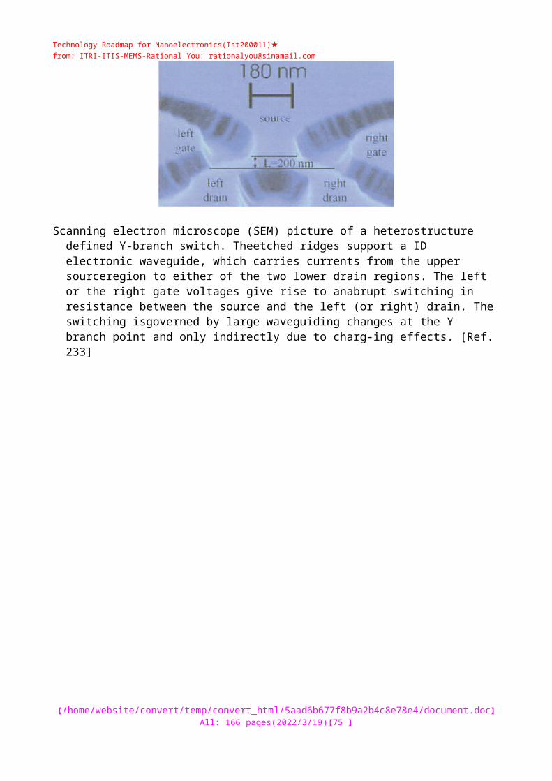
Technology Roadmap for Nanoelectronics(Ist200011)★from: ITRI-ITIS-MEMS-: [email protected]
ontothe quantum dots. The presence of leads prevents straightforward lateral branching from a chain of cells,one of the basic features, which would be needed to create logic gates.Limitations on the operating temperature are due to the weakness of the dipole interaction between thecells, which must be significantly larger than kT. The maximum operating temperature for a chain of sixcells in SOI (silicon-on-insulator) (thick line) and in GaAs (thin line) is reported in Fig, 27. The results arecalculated assuming a readout time long enough to filter out fluctuations and correctly detecting the out-put for an average polarisation that is 80% of the maximum. Improvements could be achieved by shrin-king cell dimensions and by using materials with lower dielectric constant. Structures at the molecular levelwould be needed to approach room temperature operation.The current state of the art in QCA devices is represented by the implementation of a majority voting gatebased on metal-insulator tunnel junctions, operating at about 70 rnK [Ref. 5]. Coupled Si-quantum dotsembedded in a silicon oxide matrix have been fabricated by etching and subsequent oxidation of SOIwafers [Ref. 198], and their suitability for the operation in QCA cells at a few hundred mK has beenshown. Non-invasive detection of charges in coupled quantum dots fabricated in gallium arsenide he-terostructures has also been demonstrated and can be useful for the data readout procedure. Although thetechnology for a single cell has been developed and chains of cells could be produced without substantialtechnological changes, the realisation of logic gates is hampered for not finding a manufacturing solutionon how to perform the lateral branching.Because there is no charge transport, QCA may potentially consume very low power. QCA would benefitfrom the ground state computation paradigm, i.e. once a given polarisation is enforced onto the input cells,the system relaxes to the ground state and each output cell assumes the polarisation state which minimi-
ses the total energy. However, the time required for relaxation towards the ground state cannot be reliablypredicted, and if metastable states do exist the system could get stuck in one of them for a significantly longtime. A solution could be in performing a so-called "adiabatic switching", i.e. varying slowly the height ofthe potential barriers separating the quantum dots in a cell and permitting the system to evolve remainingalways in its instantaneous ground state. Such an adiabatic scheme applicable to conducting dots embed-ded in an insulating matrix has been proposed [Ref. 212], but again here, achieving reasonable tunnellingrates would require a layout that is beyond current technological capabilities.In the future, QCA cells could be built with single bistable molecules, i.e. molecules in which, in theabsence of an external electric field, some of the valence electrons can localise with equal probability on twodifferent groups of bonds. By analogy to the four-dot cells, the presence of an external electric dipole fieldwould make one of the two possible configurations energetically favourable. The scientific challenge is toarrange the molecules in structured arrays on some substrate. If successful, the limitations due to fabrica-tion tolerances would be overcome, as molecules are intrinsically precise and bound electrons are suffi-ciently localised to act as "excess" electrons, without the need for external leads. Stray charges still representa major issue, unless it becomes possible to develop substrates virtually free from them.A novel approach arises form recent results on magnetic nanostructures demonstrate the propagation of amagnetic polarisation state along a I D chain of dots [Ref. 44]. If operation of 2D arrays would be possi-ble with these magnetic nanostructure systems, this offers a new opportunity to implement a whole QCAcircuit.Summarising, it can be said that the QCA operation principle functions and will probably demonstratedin various material systems, but it is unlikely that logic circuits will ever be fabricated, mainly due to fa-brication limitations. Possible future applications of the QCA principle would rather exploit its extremecharge sensing dependency for sensitive charge detectors. Applications for logic devices would again attrac-tiveness in the case of major breakthroughs in the arrangement ofbi-stable molecules or in
【/tt/file_convert/5aad6b677f8b9a2b4c8e78e4/document.doc】All: 107 pages(2023/5/6)【75 】
Technology Roadmap for Nanoelectronics(Ist200011)★from: ITRI-ITIS-MEMS-: [email protected]
demonstratingmagnetic polarisation in 2D structures.
5.3. Current Trends in Novel System Architectures 5.3.1. Starting Point: Systems on chip and Innovations in
Microprocessor DesignsThe superscalar RISC (Reduced Instruction Set Computer) architecture is currently the dominant
micro-processor architecture. Due to its prevailing position in the commercial microprocessor market (includingx86-compatbile processors with certain internal RISC processing) it will be undoubtedly the starting pointfor all innovations in the direction of complete systems-on-a-chip as well as for more speculative architec-tures. The characteristic feature is an instruction level parallelism based on multiple execution units andthe capability to simultaneously fetch and decode 2-4 instructions with a fixed (32 bit) format [Ref. 96].Pipelining subsequent instructions increases the efficiency and the data throughput. To avoid pipeline stallsduring conditional branches modern RISC processors often contain a branch prediction unit. On chipinstruction and data cache is part of the memory hierarchy and the classical method to solve the processormemory speed bottleneck. The sophisticated interaction between extracting instruction level parallelism inruntime and keeping the processor working complicates the design due to hazards and interrupts,Therefore, increasing the degree ofsuperscalarity to values above 8 seems not to be sensible, even for futuregenerations of CMOS.
Figure 28: Intelligent RAM Chip (IRAM)
The IRAM combines multiple vector processing units for multimedia applications, a convention-al CPU and a large on-chip memory [Ref. 121].With the increasing relevance of multimedia data processing and low power portable devices for commu-nication VLIW- architectures (Very Long Instruction Word) and Single-Instruction Multiple Data (SIMD)type instructions are developed to enable an efficient real time computation of 8-16 bit audio and videodata streams. Even for nanometer scaled CMOS more radical system architectures are being investigatedto exploit the capability of integrating I billion transistors on a single chip. Based on technological progressRISC cores are combined with vector processing units, DSPs, and large on-chip DRAM. In that contextthe "Intelligent RAM (IRAM)" (see Figure 28) is a potential solution to limit the impact of the increasingDRAM-processor speed bottleneck and to increase the performance power dissipation ratio. In nanoelec-tronics the data-path-orientated, scalable design of multiple vector units is interesting because of its simplecontrol logic and its modular design which ease the interconnection problem and the design complexity.The idea behind all these modern microprocessor architectures is to ensure that the multiple executionunits and pipelines are always used with maximum efficiency to justify the costs of the expensive circuitry
5.3.2. Parallel Processing If the number of devices on a chip increases there are roughly speaking two different strategies to
design aprocessor, namely a single powerful CPU with large on-chip memory or to use multiple CPUs or func-tional units of lower complexity. The RISC and VLIW processors mentioned above belong to the first class.However, if future processor design is evaluated from the point of view of nanoelectronics, a replication ofsimple units could be attractive to implement parallel computing schemes. Today, for servers and desktopworkstations the change of the typical workload to multiple independent processes has motivated so-called"multiple thread"
【/tt/file_convert/5aad6b677f8b9a2b4c8e78e4/document.doc】All: 107 pages(2023/5/6)【76 】

Technology Roadmap for Nanoelectronics(Ist200011)★from: ITRI-ITIS-MEMS-: [email protected]
architectures, where parallelism is exploited between concurrently running tasks and notwithin a single algorithm. Consequently, multiple execution units are more independent of each other andthe power/area consuming circuitry (bypassing, register renaming, etc.) can be avoided in favour of a sim-ple design. In the following, various architectures for parallel computing are discussed, starting from lessrevolutionary concepts up to neural networks and quantum computing.
5.3.2.1. Propagated Instruction ProcessorAmong different concepts for parallel computing the Single Instruction Multiple Data
architecture(SIMD) is a classical concept for special purpose computation assumed that there is a sufficient amount oflocality in the algorithm which has to be implemented. The regular design and local system-level inter-connections are attractive for nanoscale integration and also helps to close the design productivity gapbecause a single functional unit of limited complexity is replicated in a 2-dimensional array topology.SIMD array processors are a well-known architecture for image and vision processing tasks where a simplemapping of the algorithm on hardware is possible. However, the classical SIMD architecture suffers fromthe drawback that the instructions for the different image processing tasks have to be transmitted in a glo-bal fashion to each processing unit. The interconnection problem originating from the global instructionflow can be solved by a so-called Propagate Instruction Processor (PIP) (Figure 29 and Ref. 63). The PIPdiffers from a classical SIMD-processor in the sense that instructions are pipelined in a horizontal direc-tion while the PIP units perform their computations (Figure 29). Thus, multiple image processing algo-rithms are simultaneously solved in parallel. Without going into details, the pipelined operation wouldimprove the overall system performance if high bandwidth communication with external components wasavailable. To store the propagating instructions each processing unit contains a local instruction pipelineregister. Further components are the local memory, a control pipeline, a register, and the arithmetic logicunit. The size and capabilities of a single processing unit depend on the complexity of the algorithms andthe image resolution.
Pip Array
PIP Element
OverallControlInput
ControlInputs
ControlOutputs
Data I/O
Figure 29: Propagated Instruction Processor
【/tt/file_convert/5aad6b677f8b9a2b4c8e78e4/document.doc】All: 107 pages(2023/5/6)【77 】

Technology Roadmap for Nanoelectronics(Ist200011)★from: ITRI-ITIS-MEMS-: [email protected]
5.3.2.2. Reconfigurable Hardware: From Reconfigurable Microprocessor Arrays to Defect Tolerant Circuits
The Reconfigurable Architecture Workstation (RAW) is a replicated architecture of identical processingelements. Each processing element contains a RISC-like pipeline, a local instruction and data memory[Ref. 222]. The complexity of a processing element is comparable to a R2000 CPU and comprises about2 million transistor equivalents. The interesting feature for nanoelectronics is that the programmer canmodify the logic functionality by means of the configurable logic blocks in addition to programming theCPUs. The programmable crossbar switches allow it to implement different point-to-point interconnec-tions and to change the on-chip interconnection topology. Since the configuration of the crossbar switch-es is stored in a memory block, the RAW machine is a dynamic and adaptive architecture. Thus, althoughthe processing elements are arranged in a 2-dimensional array topology the RAW machine is not limitedto SIMD typical tasks as the PIP. The implementation of these programmable interconnects requires about30 percent of the total chip area.
Figure 30: The Reconfigurable Architechture Workstation (RAW)
The RAW machine is a one-chip reconfigurable computer architecture. Each processing elementcontains a local instruction memory, data memory, registers, ALU, control logic. The SMEMblock stores the configuration ofthe programmable crossbar switch. Besides the advantage of the regular la/out, the underlying idea of the RAW architecture is to transfer cer- tain tasks from hardware to software. For example the testing procedures of a billion transistor chip can be reduced because reconfiguration and re-routing, in the case of defective elements, is performed by a com-piler running on a host computer. Furthermore, for application specific
【/tt/file_convert/5aad6b677f8b9a2b4c8e78e4/document.doc】All: 107 pages(2023/5/6)【78 】

Technology Roadmap for Nanoelectronics(Ist200011)★from: ITRI-ITIS-MEMS-: [email protected]
tasks, a significant increase in speed over a pure software solution is achieved by exploiting the local configurable logic blocks,Defect tolerant architectures may be essential for computational nanoelectronics since this is probably theonly way to build systems with billions of devices economically. Any computer with nanoscale componentswill contain a significant number of defects, as well as massive numbers of wires and switches for commu-nication purposes. Using field-programmable gate arrays (FPGAs) there are different approaches to defecttolerant custom configurable computer:(1) the Teramac [Ref. 94], a defect tolerant custom configurable computer based on field programmablegate arrays (FPGAs) where reprogramming is achieved off-line by means of an external configuration work-station. The fundamental paradigm of the Teramac is to build a computer cheaply and imperfectly, findthe defects, configure the resources with software, compile the program, and then run the computer. Here,the underlying idea is a redundant interconnection structure, such as the fat tree architecture shown inFigure 31.(2) more recently, "embryonic electronics" is discussed as a biological inspired paradigm which differs fromthe Teramac in the sense that the reconfiguration algorithm is performed on chip in form of an "artificialgenome" containing the basic configuration of cell. According to van Neumann's famous idea of self-repro-ducing automata the characteristic feature of "embryonic electronics" is to incorporate basic biologicalprinciples such as self-replication and self-repair into VLSI [Ref. 137]. The purpose of this approach is notto model and explicate biology but in a long term to develop methodologies of performing computationusing imperfect components without external supervisor.Although both ideas are similar to the RAW machine, from the viewpoint of the underlying circuitry theydiffer in the sense that a computation is performed on the basis of programmable look-up tables or in basic"cells" composed of programmable multiplexers instead of complex Boolean logic circuits. If a nanoscalecircuit technology allows an efficient implementation of memory components (while logic circuits aremore difficult to fabricate as in the case of SET logic and non-volatile SET memories), the lookup tableapproach of the Teramac could be an alternative to the traditional way of building a computer using logiccircuitry.
Overall, we can draw several important conclusions for nanoelectronic systems: First, it is possible to build apowerful computer that contains defective components, as long as there is sufficient communication band-width in the system to find and use the working components. Second, the resources of a processor must havea sufficiently high degree of connectivity and of technical intelligence. In the Teramac the technical intelli-gence is given by the configuration workstation whereas in Embryonics each cell contains the necessary setof rules. The third aspect addresses the issue that the most essential components for nanoelectronics may bethe address lines and the crossbar switches that control the settings of the hardware configuration.Since the configuration algorithm, either running on the host-workstation or stored inside a cell, is basi-cally software, the strategy of implementing the wide range of application specific tasks in software, whilemaintaining general purpose integrated circuits, follows the original idea of behind the first microproces-sor. The continuation of hardware-software co-design in nanoelectronics is likely to continue due to theexisting knowledge and the economic success of the semiconductor industry. In summary, reconfigurablehardware suggests a different approach to nanoelectronic research, it is a top-down approach, and not abottom-up approach dominated by the technology. Nevertheless, it has to be still demonstrated that theloss in area efficiency due to the hardware overhead in the fine grain FPGA@ is compensated by reduceddesign, fabrication and testing costs.In addition to reconfigurable concepts, other classical techniques, such as triple modular redundancy, haveto be considered to tolerate transient errors during operation, which is extremely important for QCAs andSETs in the presence of fluctuating offset charges. At the current state of technology the detection of tran-sient errors, that is fault-tolerance, seems to be a
【/tt/file_convert/5aad6b677f8b9a2b4c8e78e4/document.doc】All: 107 pages(2023/5/6)【79 】

Technology Roadmap for Nanoelectronics(Ist200011)★from: ITRI-ITIS-MEMS-: [email protected]
rather a problem of circuit design. In other words, the cir-cuit implementation of the programmable switch in Figure 31 should be robust against these transienterrors even if the whole hardware has detected no defective components.
Figure 31: Redundant Interconnections of the Teramac.
5.3.3. DNA Computing ■ Computations by chemical or biological reactions overcome the problem of parallelism and
interconnec-tions in a classical system. In DNA computing [Ref. 1] where the similarities between mathematical oper-ations and biological reactions are used to perform calculations, the key idea is to find the similaritiesbetween DNA (Deoxyribo Nucleic Acid) - the basic genetic information - and well known digital com-puters. If a string of DNA can be put together in the right sequence, it can be used to solve combinatio-nal problems. The calculations are performed in test tubes filled with strands of DNA and gene sequenc-ing is used to obtain the result. Adieman calculated the travelling salesman problem to demonstrate thecapabilities of DNA computing. DNA computing on parallel problems potentially provides 10 "* MIPSwhile using less energy and space than conventional supercomputers. While CMOS supercomputers ope-rate 10 @ operations per Joule, a DNA computer could perform about 10 " operations per Joule (10 '@ times
more efficient). Data could potentially be stored on DNA in a density of approximately I bit per nm " while existing storage media as DRAMs require 10 @ nm" to store I bit.
5.3.4. Artificial Neural Networks Popular concepts of parallel and adaptive computing are the various forms of artificial neural
networks [Ref. 93]. Again biological information processing motivates this approach, but in contrast to DNA com- puting the learning algorithms are formulated as complicated sets of mathematical equations. These equa- tions are implemented in conventional hardware or in software if flexibility is more important than execu- tion time of the neural algorithm. Due to the fundamental relevance of the adaptive interconnection, these large arrays of simple neural pro- cessing elements show features such as association, fault tolerance, and self-organisation. Here, it has to be considered that on the one hand the complexity of a neural processing element is much lower than the complexity of the processing elements in the Teramac or RAW machine discussed above. On the other hand the interconnection density of neural processing elements is orders of magnitudes higher, so that the question if artificial neural networks are appropriate for
【/tt/file_convert/5aad6b677f8b9a2b4c8e78e4/document.doc】All: 107 pages(2023/5/6)【80 】
Technology Roadmap for Nanoelectronics(Ist200011)★from: ITRI-ITIS-MEMS-: [email protected]
nanoelectronics remains open. As a starting point, a neural nanoelectronics architecture with a low interconnection density, such as cellular neural networks (CNNs) and associative matrices are interesting [Ref. 74] even if their capabilities in regard to adaptation and generalisation are limited. CNNs are regular processing arrays where only the neighbouring cells are connected. Often these processing elements are implemented in analogue circuit techniques so that low power applications, such as intelligent sensor pre-processing are preferred applications. To a certain degreethey can be regarded as low-level SIMD architectures and therefore suffer from the same disadvantage of aglobal instruction distribution. The associative matrix is a concept for a distributed memory and is basedon digital input and output states. The learning rule is strictly local and only binary weights are used. Dueto the distributed storage principle and a certain degree of fault-tolerance, the associative matrix could beinteresting for a multi-GBit RAM made of single electron technology.The phenomenon of self-organisation is similar to self-structuring in technology [Ref. 60] aiming at pro-ducing nanometer scale structures without extensive processing steps from outside. The self-organisingneural network maps the input data on a two-dimensional area without a teaching help from outside [Ref. 117]. This property would be useful in nanoelectronics for structuring an initially homogeneous array ofcells.Most of the present neural networks are static networks. In a first step they map the data according to learn-ing algorithms. In the second step the adaptive interconnections are fixed and novel, unknown data is clas-sified or associated based on the internal configuration. Alternative approaches are time dependent, biolo-gy inspired networks in which the input data is processed in a dynamic way using dynamical phenomena,such as spiking, oscillations, bifurcations, and local excitations. Local adaptation and excitations occuraccording to non-linear integral-differential equation for the time variant weight connections and the cellpolarisation (excitation). These dynamic networks, known as resonant neural systems, not only show out-standing new features of artificial intelligence similar to small brains but also need a tremendous numberof devices if an implementation is intended. At this point it should be noted that neural networks are asupplement and not a replacement of traditional data processing if a useful application can be found. Inthis way, a certain self-adaptation of neural networks can compensate the inherent drawbacks of nanoelec-tronic devices, for example fluctuating background charges ofSETs are presently under investigation [Ref.75]. Nevertheless, the huge interconnection density as basic paradigm of large scale multi-layer neural net-works is contradictory to the low driving capabilities of many nanoelectronic devices because each neuralnode has to be connected to at least 10-100 synapses for a useful computation. Eventually SET-MOSmemories could be used for an area efficient implementation of the synapses for long term storage of theweight connections. If the required precision of about 8-16 bit can be achieved remains an open question.
5.3.5. Quantum Information Processing (QIP) Quantum computers process information in a completely different way than microprocessors and
use-quantum algorithms that do not have classical analogues. From a physical point of view a bit is a two-statesystem, in which one of two distinguishable states, representing two logical values, is occupied. Now, quan-tum mechanics tells us that if a bit can exist in either of two distinguishable states, it can also exist in cohe-rent superpositions of them, a so-called qubit. Moreover, an array ofqubits can exist in a superposition of
configurations representing different values, such systems are called entangled, as the state of one qubitdepends of the states of other qubits. During a 'gate operation, a time evolution of the system, each valuein this entangled system is affected, so we are performing a massive parallel computation. This intrinsic pa-rallelism can have a revolutionary impact on the handling of
【/tt/file_convert/5aad6b677f8b9a2b4c8e78e4/document.doc】All: 107 pages(2023/5/6)【81 】

Technology Roadmap for Nanoelectronics(Ist200011)★from: ITRI-ITIS-MEMS-: [email protected]
complex algorithmic problems, like the tra-velling sales man problem or, an example important for cryptography, the factoring of integers, that isproblems that scale exponentially with the size of the input (non deterministic polynomial problems NP).QIP systems still need to demonstrate registers for tens (and ultimately hundreds) of qubits. Systems ableto operate with a few qubits, have been demonstrated with NMR of small molecules or quantum photoninterferometry, and in particular with ions held in traps. At present it is impossible to predict the winningtechnology for QIP, since all existing approaches show severe limitations, in particular the problem of deco-herence, i.e. the destruction of the entanglement due to non-controlled interactions with the environment.A viable technological approach should have the following properties:I, Demonstrate gate operations based on entanglement,2. Possess a mechanism for writing and reading of data,3. Availability to control decoherence and perform fault tolerant operations,4. Be scalable in terms of number of qubits.Solid state demonstrators, to compare with in the frame of this roadmap, do not exist. At present, most ofthe initiatives have to work towards demonstrating single-gate operations. The biggest challenge appears tobe the mastering of decoherence. This poses very stringent manufacturing requirements, which are beyondpresent day capabilities. Ultimately one hopes that solid state devices are better scalable than QC based onatomic physics which for the time being are the only devices capable of demonstrating at least 6 qubit re-gisters.Different venues to a solid-state based QC are proposed [Ref. 179].:Quantum-dots based QC: atom-like quantised excitations of electrons within a quantum dot serve as a sin-gle qubits. These excitations have energy spacing larger than temperature spacing. From an experimentalpoint of view progress has been made by using a one-photon forbidden transition to implement the qubitin order to avoid spontaneous emission, but major problems still remain to control decoherence, via e.g.phonon interactions. This concept requires evenly spaced energy levels between all quantum dots, whichtranslates into very stringent manufacturing specifications that are difficult to meet with current technolo-gy. Entanglement of two quantum dots occurs via a state dependent interaction based on an overlap of theelectron wave functions in different quantum dots. This interaction mechanism is not yet understood anddepends on a tight spacing of the quantum-dots, which again poses considerable technical challenges.Electron Spin based QC: the concept relies on the spin-spin interaction of two different electrons. Oneof the physical implementations under investigation is to fix the electron within a quantum dot. Here it isin particular the capacity to control the interaction between qubits (necessary for entanglement) whichposes a great challenge. An alternative approach is to achieve entanglement via photons in a cavity in whichthe quantum dots are placed. The read out is generally made via Electron Spin Resonance (ESR).Superconducting devices: Solid-state low Tc Josephson junctions will serve as quantum logic gates; alter-natively the charge or flux circuit states, that at low temperatures behave quantum mechanically, will serveto implement the qubit. One can use external potentials on gate electrodes or external magnetic fields tovary the quantum mechanical coupling in the systems, and tune the coherent superposition of the circuitvariables. These circuits can be fabricated using standard electron lithography techniques, most appropriatefor physical implementation. Recently, it was shown that the manipulation of Josephson junction qubits ina quantum coherent way over several nanoseconds was possible [Ref. 155]. It is forecasted that the func-tioning of a XOR gate and a circuit entanglement using superconducting tunnel junction technology willbe possible in 2003.Nuclear Spin based QC: The qubit could be implemented by the nuclear spins of P- donor atoms in apure Si host crystal [Ref. III]. A gate over each donor atom controls the qubits, while a second gatebetween qubits controls the height of the potential barrier and thereby the extension of the electronic wavefunctions. In this way the interaction between the nuclear spins is controlled through the electron spin-exchange and thereby also the interaction between the two qubits. For the implementation of this idea,gates of order of 10 nm are required with dopant spacing of 20 nm that are not possible to manufacture
【/tt/file_convert/5aad6b677f8b9a2b4c8e78e4/document.doc】All: 107 pages(2023/5/6)【82 】

Technology Roadmap for Nanoelectronics(Ist200011)★from: ITRI-ITIS-MEMS-: [email protected]
with present technology. This idea is rather favourable concerning decoherence (as the nuclear spin is wellshielded within the silicon host crystal); the main problem here seems the complicated state read-out via a spin transfer mechanism of information from the nuclear spins to electron spin.A modified version of the aforementioned proposal is the use of the electron spin rather than the nuclearspin of the P donor atom. This modified concept is based upon using the change in g-factor (which quan-tifies the coupling of the spin to an applied magnetic field) between Si-rich and Ge-rich heterostructures. Placing a P donor between two conduction band barriers, an electron may be trapped in the vertical direc-tion. The material between the two barriers is designed to have the same conduction band discontinuitybut one is a Si-like band (D2 valley with g= 1.998) while a second layer is Ge-like (L valleys with g= 1.563),Then electrostatic gates are used to move the electron from a region of high g. The higher dielectric con-stant and lower effective masses compared to bulk Si potential would allow each qubit to be of order of200 nm in size, which is feasilble with present lithographic techniques. This alternative would allow highfabrication tolerances and permit an easy read-out via ESR, rather than the difficulty to measure nuclearspins. The drawback of the electron spin approach is that the decoherence is more difficult to master thanthe nuclear spin option.Within the next two years one can hope to identify the more promising candidate systems, but most like-ly one cannot expect multiple gate operations from solid state devices for another couple of years. For thetime being implementations in atomic physics are the systems of choice to explore the limits of quantumcomputing.
5.4. Comparison of the Various System Architectures A rough overview of different architectures and circuits discussed in this chapter is shown in Figure
32 [Ref.63] Classifying different popular computational paradigms, some characteristic features that become rele-vant in nanoelectronics "lie the amount of wiring, the degree of parallelism, and the range of data transfer(Figure 33). The difference between wiring and data transfer is that the first uses physical interconnections,that is, metallic wires, whereas data transfer may be realised without direct physical wiring. In this case,long range data transfer is done by sending a signal from module to module, analogous to systolic struc-tures. It is obvious that, today, parallel operation and locally interconnected modules arebfiess significancein traditional microprocessor memory architecture. In contrast, the basic elements of cellular automata andartificial neural networks process the given input data fully parallel. Additionally, Figure 33 specifies theregion of highly parallel operating and locally interconnected nanoelectronic systems.Since this document primarily investigates novel devices, the question of suitable architectures can only beconsidered indirectly. Nevertheless one result of this short review of the different systems is that each archi-tecture relies on an efficient implementation of several basic circuit functions. In this respect,table 13 summarises the corresponding key components and suggests an appropriate technology as well asa prototype circuit of lower complexity. For example the RAW machine and Teramac make intensive useof programmable crossbar switches and thus a prototype SET or RTD implementation would demonstratethat nanoscale technology is able to deliver such a key component. By combining experimental simulationresults it then possible to extrapolate the performance of larger circuits and systems. To handle the increaseddiversification and to cope with design complexity it is expected that intelligent design tools will becomemore and more important within a hierarchical design flow which is characterised by interfaces with designrules and standardised functional blocks.
【/tt/file_convert/5aad6b677f8b9a2b4c8e78e4/document.doc】All: 107 pages(2023/5/6)【83 】

Technology Roadmap for Nanoelectronics(Ist200011)★from: ITRI-ITIS-MEMS-: [email protected]
CIRCUIT DESIGN'3Proceears
Novel Cornputii-o
DEVICESPerformanceDfndty DtMng capa.d1yPower Error toes
NANOELECTHONIC 'SVSTEM' AttCHrTECTURES
Figure 32: Aspects of Architectures for Nanoelectronic Systems
FAULT TOLERANCETriple Mmiulai RedUririBnc)' [-Ptecontiguifltlon [-Ofta Rt-duncia-io- @Fa@Jtl@<o@elan@Plogra@@@i @-
APPLICATIONSPfocess CortiolhReai-tir@.@ signal pro<@aa@1-1 Selt-teaming Syaeme@
SYSTEMARCHITECTURESPef*on"anceParallellwf@wef ConaumiJtiofiln@ercorinwionerSIMD-MP@iM tM D Mi ico@roceefew@Vecioi
【/tt/file_convert/5aad6b677f8b9a2b4c8e78e4/document.doc】All: 107 pages(2023/5/6)【84 】

Technology Roadmap for Nanoelectronics(Ist200011)★from: ITRI-ITIS-MEMS-: [email protected]
Piocasaolft@rNeural Ne!'@@*e@
Table 13: Components of Nanoelectronic ArchitecturesArchitecture Key Component Technology Prototype Circuit
DesignsSuperscalar
RISC,VLIWMulrithreadprocessor
ALU, Registers, Cache
nm-CMOS Adder, multiport SRAM cell
System on-chip,IRAM, PIP Non-volatile (NVLM)memory,fast RAM
SET, MRAM,FRAM,low power RTD
SET-M06 NVLM arrayDRAM cell in CMOS logicprocessbistable RTD circuit
DSP, MultimediaUnits Multiplier Accumulator
nm-CMOS Logic,RTD
Array multiplier cell,accumulator,Pipeline stages
RSFQ Functional Units LTS Pipeline stages forsupercomputer
CommunicationASICs Crossbar Switch RTD andOptoelectronics
GHz-Latches, MUX
IRAM Vector Unit RTD, nm-CMOSLogic
high bandwidth pipelinedALU
RAW, Teramac Crossbar Switch,Functional Unit
nm-CMOS, SET,RTD-CMOS
Programmable TransmissionGate with local SRAMNonvoltatile SET-memorycellSRAM or NVLM based look-up table
Evolvable Hardware Genetic ConfigurationUnit (FPGA-like)
SET, QCA, ME Cellular automata randomnumber generator
Neural Network Neural processingelement, synapse
QCA, SET Discrete-time CNN cell,SET-MOS memory cellsynapse
The key components of possible nanoelectronic system architectures depend upon the prototypeimplementation of basic circuits for different technologies.
parallelprocessingCNN Cellilar Neural NetsNS Nanoelectronic SystemsANN Artificial Neural NetsAP Array
Processors(jP Microprocessors'@global
Figure 33: Comparison of Architectures
【/tt/file_convert/5aad6b677f8b9a2b4c8e78e4/document.doc】All: 107 pages(2023/5/6)【85 】

Technology Roadmap for Nanoelectronics(Ist200011)★from: ITRI-ITIS-MEMS-: [email protected]
Comparison between Cellular Neural Networks (CNN), ANN Artificial Neural Networks (AP),Array Processors (AP) and Microprocessors (ftP) in respect to data transfer, wiring and parallelprocessing. A Nanoelectronic System would require low wiring, parallel processing and ideally aglobal data transfer.
【/tt/file_convert/5aad6b677f8b9a2b4c8e78e4/document.doc】All: 107 pages(2023/5/6)【86 】
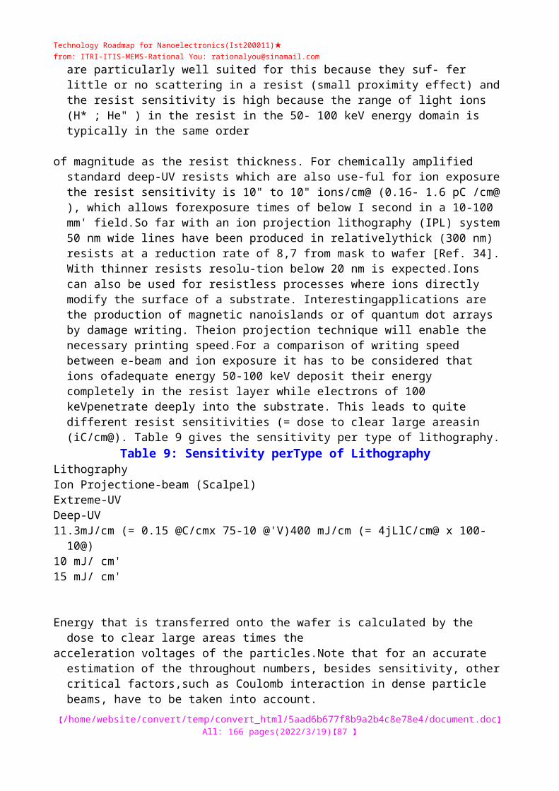
Technology Roadmap for Nanoelectronics(Ist200011)★from: ITRI-ITIS-MEMS-: [email protected]
6. Conclusions In the past 15 years, nanoelectronics has developed as into a versatile and fruitful playground for
manyinnovative device concepts. Only a few of the concepts developed have been discussed in this Roadmap.Those working in the field have certainly witnessed that many novel ideas have not survived a first criticalexamination of their applicability on an industrial scale. The concepts discussed in this document are forthe largest part those that could eventually make it to applications, although some others may, within a fewyears, turn out to be simply the fashion of the year 2000 and the willingness of the editor to include them.Not withstanding these observations, this document compiles, to the best of out knowledge, a commonwisdom shared among the majority of researchers in the field from theMELARI / NID projects.One thing, which has become clear from this exercise, is that Si MOSFET technology still has many yearsto go. Even if downscaling would eventually slow down over the next decade, generations of performanceimprovement are still to be obtained from utilising more advanced architectures. However, there are cleartechnological limits to MOSFET, such as power consumption or complexity, but more important perhapsare economical considerations, including the huge investments costs or the risk of a Jow return in invest-ment. For these reasons, the novel devices discussed in this Roadmap deservedly receive strong attentionfrom the research community. RTDs and spin devices are on the verge of commercialisation. SET deriveddevices in the form of nano-flash devices seem a most natural successor for several RAM technologies.RSFQ could provide powerful computing capability, provided that one is prepared to pay the price of cryo-genic operation. Molecular electronics is still at an immature stage but deserves vigorous investigation inview of its huge potential.Fabrication technologies developed for manufacturing nanodevices provide a much more direct spin-off tothe electronics industry, since they can be equally well applied to MOSFET fabrication. In fabrication it isremarkable that the work generated by the semiconductor industry, in this case optical lithography, hasshown a much longer life than predicted even by its greatest advocates five years ago. Bottom-up approa-ches, closely linked as they are to the field of molecular electronics, are elegant, cheap and possibly enor-mously powerful techniques for future mass replication, but their applicability remains limited until totalcontrol over the emerging structures in terms of wiring and interconnections can be obtained. It is clearthat new architectures are required for such bottom-up fabrication approaches.Similar to fabrication, architecture development has also direct bearings for the Si electronics industry andis a field where much ground remains to be gained. At the same time, the specific quantum mechanicalproperties of many nanodevices require radically novel architecture approaches, and it is gratifying to seethat such approaches are now starting to be introduced by the architecture experts. Concepts like fault to-lerant architecture, parallel processing, local architectures and neural nets are directly translatable into Sihardware, whereas more advanced concepts like non-dissipative and quantum computing will almost cer-tainly require the implementation of novel quantum mechanical nanodevices.
6.1. Devices The list of devices discussed in this Roadmap has been limited to those presently under
investigation aspossible nanoelectronic circuit elements. As time goes by, other device concepts may have to be added tothose in this list while some others may disappear.SET at present shows promise for memory, probably not in the form of a single electron transistor butrather as a nano-flash memory. As such it seems a natural extension for conventional flash type memorydevices and may even take over from SRAM, possibly bridging the gap between more standard CMOS andthe actual single electron transistor. Whether the actual single electron transistor itself will
【/tt/file_convert/5aad6b677f8b9a2b4c8e78e4/document.doc】All: 107 pages(2023/5/6)【87 】
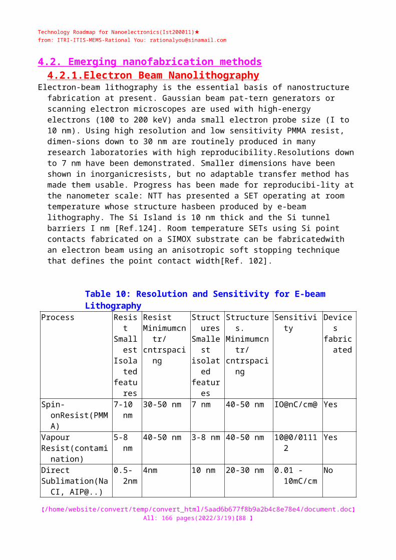
Technology Roadmap for Nanoelectronics(Ist200011)★from: ITRI-ITIS-MEMS-: [email protected]
ever make it tothe market place will strongly depend on future developments in device fabrication, both in respect to fea-ture size (2 nm range) and uniformity, along with the control of background charges. The charge sensiti-vity of the devices also imposes strong limitations on the allowable electrostatic interaction between diffe-rent devices in a ULSI circuit.RTDs are the most mature of all the device technologies reviewed in the present Roadmap. III-V devicesare expected to be on the market in the near future. Research on Si-based devices still requires further deve-lopment before marketable devices can be realised. The major concern remains wafer uniformity, especial-
ly for large integration levels. First applications will most probably be high frequency DACs or ADCs and transmitters, along with ultra low power memory for portable applications. It should be noted that the intrinsic bistability ofRTDs also enables the implementation of compact and elegant architectures for logic circuitry although these areas are not as mature as the lower integration level applications. RSFQ has potential in niche applications, where high speed and computational power are important and the cost of cryogenics may be tolerated. One of the major problems is interfacing the high-speed circuitswith conventional CMOS for input / output, especially when the large difference in circuit speeds is con- sidered. At present the technology for low temperature superconductors seems mature, while for HTS, although considerable progress has been achieved in recent years, large-scale integration has not been demonstrated yet. The market presence of RSFQ will also depend on the availability of reliable, low-cost cooling engines. Molecular electronics is at present taking off as a branch of transport physics. Its potential is large but there are formidable obstacles, which must be overcome. Here it seems of the utmost importance that chemists, biologists, physicists and engineers develop an interdisciplinary platform for communicating the needs of the electronics industry in one direction and the possibilities of chemical synthesis and self-assembly con-cepts in the other.Spin devices in the form of tunnel junction MRAMs will be on the market in the near future. Recordingheads based on the tunnel junction exchange biasing mechanism are already existing applications. A pro-blem for widespread use in the semiconductor industry is that the metals used in the devices fabricated todate are not compatible with CMOS lines. Spin injection in semiconductors has considerable potential, forexample, in quantum computing.A comparison between the device technologies presented in chapter 3 and the CMOS developments pre-dicted by ITRS has been attempted and is presented in Table 14 to Table 23. While the ITRS forecasts forCMOS are based on extrapolations of the last thirty years of continuous progress along with recent researchresults, the nanoelectronic devices are best guesses by the researchers participating in the MEL-ARI / NIDprojects. The values on nanodevices shall serve as a guideline for a discussion basis to monitor the progressin the nanoelectronic field.
6.2. Fabrication To date most of the gate and circuit downscaling depends on the ability to push optical lithography
tosmaller and smaller dimensions. Given the existing investments in optical lithography, it will remain thepreferred manufacturing technique for CMOS as long as economically or physically possible. It seems rea-sonable to expect that serial techniques will not be suitable for mass fabrication at high integration levels,although some may still be applicable to metrology and testing. For the next one or two generations beyondoptical lithography, there are a number of options that are being investigated and still need further researchsuch as EUV, X-ray, imprint, projection electron beam or projection ion beam lithography. These tech-nologies are now all under active evaluation and are all-compatible with the devices discussed in thisRoadmap. To date X-ray and projection electron beam lithography have had the greatest investment
【/tt/file_convert/5aad6b677f8b9a2b4c8e78e4/document.doc】All: 107 pages(2023/5/6)【88 】

Technology Roadmap for Nanoelectronics(Ist200011)★from: ITRI-ITIS-MEMS-: [email protected]
inresearch. Once structures of nanometer size dimensions and ultra-tight tolerance are required (such asSET), it seems unlikely that there will be another manufacturing approach apart from the bottom-up tech-nique. As was stressed before, however, in the bottom-up approach a considerably stronger degree of con-trol on the architecture by the engineers is necessary to enable actual circuit fabrication. The first applica-tions of the bottom-up technique are likely to be small circuits fabricated on top of top-down fabricatedchips.
6.3. Architectures For the development of alternative circuit to CMOS, it is of supreme importance a collaboration
betweendevice physicists and architecture designers starts early. For instance. It is important for device physicists torealise the consequences of a gainless device on the circuit architecture that must be implemented if thedevice is going to be used in applications. Another issue often missed by device people is the rapid increasein the timing (clock frequency) when dimensions are reduced and speed is increased. The arrival of localarchitectures, parallel computing and defect and fault tolerant architectures are a direct consequence of thisdrive towards miniaturisation and apply as well to CMOS as to the nanoelectronic devices discussed in this
Roadmap. As long as nanoelectronic devices operate in a classical regime, the architectures could be verysimilar to those for CMOS devices of similar dimensions. A development towards embedded systems com-bining logic and memory on one chip, quite natural seems moving away from the standard CPU / me-mory architecture. As soon as quantum mechanical concepts are required at the device level, however, dif-ferent approaches to system architecture are needed. For RTDs this leads to a reduced system complexitywhile for the QCA implementation of SET this leads to quite involved but additionally quite compact cir-cuit architectures. Totally novel architectures will be needed for relatively young concepts such as quantumcomputing, where at present research focuses mainly on the basic device and circuit level.
6.4. Outlook While CMOS continues to dominate the semiconductor industry, it is apparent that several
nanoelectronicdevices originally conceived as successors to CMOS, are now finding their way into niche markets. It is alsoclear that the Moore's Law, exponential increases in density and performance, that CMOS has enjoyed forover thirty years cannot be maintained forever. No exponential increase can go on forever - eventually theincrease in density, power consumption and volume of silicon chips will require all the energy in the uni-verse to allow operation! If at some point where the exponential increase flattens out further increases inperformance is required, one or some of the devices discussed in this Roadmap (or possibly another nano-electronic concept) could find itself in the dominant position in the market place. If the nanoelectronicfield wants to mature to this stage, there is a necessity to bring novel devices more on a par with CMOSby developing the necessary fabrication processes, simulation tools and design rules that are required forany industrial electronic manufacturing process. Nanoelectronics is now coming of age, and it appears tobe the correct time to develop these production tools. This Roadmap is part of such a process of profes-sionalisation of the field.
【/tt/file_convert/5aad6b677f8b9a2b4c8e78e4/document.doc】All: 107 pages(2023/5/6)【89 】
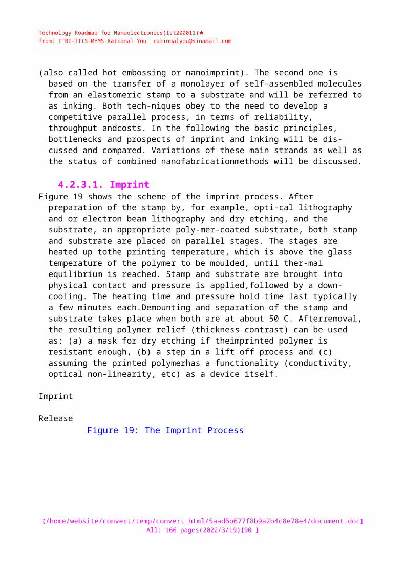
Technology Roadmap for Nanoelectronics(Ist200011)★from: ITRI-ITIS-MEMS-: [email protected]
7. Comparison Between Technologies
One of the major objectives of the Nanoelectronic Roadmap is to allow comparisons between differenttechnologies. In this section, an attempt is made to compare the technologies described in the previoussections with present production devices. In all cases, the present experimentally demonstrated per-formance in 2000 will be compared with predictions for 2006 and 2012.The first section compares memory technologies. The second section assesses the similarities and differ-ences of devices intended for logic and applications. The third section demonstrates the performance ofsingle device nanoelectronic technologies and research device performance and the fourth looks at thecircuit performance of different technologies. It is clear that it is difficult and subjective to compare cer-tain parameters especially in technologies whose devices operate in a completely different way than con-ventional transistors, CMOS, etc.. In addition, changing the supply voltage or optimising for a singleparameter may also vary the performance of individual transistors. Therefore, some standard guidelineswill be used to attempt fair comparisons between differing technologies.
7.1. Notes: General remarks: 1. Results in each column will be from a single device and hence the maximum
fT , fmax etc. fromdifferent devices are not quoted. This should give better comparisons between technologies, as onemay always maximise a single parameter to the detriment of many others.2, The power, switching time and power-delay product for devices is at the normal supply voltage ofthe circuit i.e. V@ or equivalent.3, The operating voltage is loosely defined as the standard supply voltage for operating the device orcircuit. For DRAM, V@J is an appropriate voltage, while for flash the program voltage V is moreappropriate.4. The minimum noise figure quoted for logic is at 2 GHz, as this is one of the most commonly quot-ed parameters in the literature at present, due to the mobile telecom applications.5. Transconductance, g@ or gain, P will always be the maximum value of a device.6. Both lithography and feature size are quoted for e.g. logic transistors where the effective gate lengthcan be significantly smaller than the width defined by lithography and especially for vertical tun-nelling devices such as RTDs where the critical dimension for device operation is defined by epi-taxial growth and not the lateral lithographic length. For DRAM the lithographic length will bethe half pitch.Specific notes relating to the following tables(a) Active elements; transistors for semiconductor devices and junctions for superconducting devices.CMOS microprocessors including on-chip cache.(b) An average gate contains about 5 junctions.(c) The power dissipation per gate is estimated to be - l@iW for LTS (Nb technology) and … 0,l(iWfor HTS including the bias current system containing the resistive load.(d) Excluding cooling(e) fan-in/out=3, Complex pipelined logic(f) fan-in/out=l, D-flip-flop(g) estimated from the difference between the highest occupied molecular orbital (homo) to the low-est unoccupied molecular orbital (lurno)(h) estimated that the resistance per device / molecule is in the order of I OOW.(i) the performance depends on whether some breakthrough in molecular QCA will be achieved.Without any molecular improvement, the prediction would be close to the 2006 one,
(k) HTS circuits may be operated at lower temperatures as their performance increases. For instanceat 4K, the operation speed increases by a factor 10 as the I@R@ product of the junctions increasesby ten. For these estimations, the required reproducibility spread of the junctions is 8%, whichseems realistic for interface engineered Josephson junctions.(m) The principle of semiconductor based QCA circuits have been shown and the performance hasbeen reported for year 2000. The QCA data for 2006 assumes an improvement in Si or GaAs basedcircuits. As
【/tt/file_convert/5aad6b677f8b9a2b4c8e78e4/document.doc】All: 107 pages(2023/5/6)【90 】

Technology Roadmap for Nanoelectronics(Ist200011)★from: ITRI-ITIS-MEMS-: [email protected]
explained in chapter 5.2,2, due to fabrication problems and the need to operate at verylow temperatures it is unlikely that semiconductor based QCA will come on the market and nodata is reported for the year 2012. The QCA column in Table 23 has not been removed, as theQCA architecture may be applicable for molecular concepts.(n) As discussed in chapter 3.1, if single electron devices will make it to the market then sensing appli-cations or memory are the most probable applications. The inclusion of SET devices in the logic/ high frequency tables is serve to compare the characteristics to other applications, rather thanconsidering pure SET as a alternative to CMOS MPU.(p) Resonant tunnelling devices based on III-V compound semiconductor have a very limited inte-gration density. The may be find a niche market as high speed DRAMs for military applications,due to their radiation hard nature.
7.2. Comparative Tables between alternatives for memory and logic
applications
Table 14: Comparison Memory Devices Year 2000CMOS Single
Electron' Funnelling
RTD MRAM
Technology DRAM Flash104,157]
SRAM Yano-type
Multi-dotnano-flash
Singledotnano-flash
ITHFETTSRAM
TJ GMR
Reference [237] [156] [242] [218] [49] [49]No. ofdevices IGB 256MB 6MB/cm2 128MB 1 1 16 1MBCircuitSpeed 100M@ 100MHz 200M@ 50kHz 500M@ -20MHz 100M@Feature size 180nm 180nm 200nm 250nm 100nm 500nm 250nm 350nmAcces s time 10ns 10 HS 1 ns 20ns 10ns <lns 50ns <80nsWrite time 10ns 1 ms 10 Us 100ns IMS 10 MS 10ns 100nsErase time 1 ms 10 [Us 1 ms N/A N/ARetentionTime 128-256ms 10years >10years 1 day 7 days 5s Static >10years >10yearsEnduranceCycles Infinite 10" Infinite 107 10" 10" Infinite InfiniteOperatingVoltage (V) 1.5-1.8Vdd 8Vpp 1.5-
1.8Vdd
15V 5V 10V 1-1.5V 3-5V 2-3V
Voltage toswitch states 0.2V 5V 0.2V 0.5V 0.65V 0.1V 0.38V 50 mVCell size 12P/
bit0.4ium29F2/bit 2P/bit 9F2/bit 9F2/bit 100ILlirf 2F2/bit 9P+T
No. ofelectrons 10000 1000 >10000 1000 2 1 103-10@ N/A N/AStandbyPower(W/
Mbit)10-7 200 5 None None
【/tt/file_convert/5aad6b677f8b9a2b4c8e78e4/document.doc】All: 107 pages(2023/5/6)【91 】

Technology Roadmap for Nanoelectronics(Ist200011)★from: ITRI-ITIS-MEMS-: [email protected]
Table 15: Forecast Memory Devices Year 2006
(Ref. 104 for year 20(B)CMOS
Single ElectronTunneling
RTD/ITD
MRAM Mole-cular
DRAM Flash SRAM Multi-dotnano-flash
Singledotnano-flash
RTDITHFETTSRAM <P>
ITDITSiTSRAM
TJ MechanicalGio+STM
16GB 16GB IOOMB/ cm@
16GB -1 MB/ cn@ 20MB/cm@ 128 GB 1 kB
125 MHz 125 MHz 554 MHz 500 MHz ISOMHz 250MHz 10GHz100 nm 100 nm 100 nm 100 nm 100 nm 200 nm 200 nm 70 nm 50 nm8ns 1.8ns 10ns 5ns - 10ns 5ns < 1 ns10ns 100ns 100ns 5ns -10ns 10ns < 1 ns10ns 100 Us - 5ns -10ns N/A256-512ms 10 years > 10
years1 year 5s > 10 years > 10 years > 10
years<ls
Endurance cycles infinite 10- infinite 10'@ Infinite infinire Infinite InfiniteOperatingVoltage 0.9-1.2Vdd TVpp 5 5 3-5 0.5 0.5 1.5 < 1
switchbetween 1 O.I 0.2 0.2 <50mV <l
lIPlb it0.046 Um@
9P!b it 0.21um 0.04 Urn@ 4F/b it
1 1 1000
Power(W/Mbi 0.01 10-" 105
Table 16: Forecast Memory Devices Year 2012
(Ref. 104 for year 2011)CMOS
Single ElectronTunnelling
RTD /IT D MRAM Molecular
Technology DRAM Flash SRAM SET memory
RTDITHFETTSRAM')
ITDITS;TSRAM
MRAM molecularnetwork
No. of devices 256GB 256GB ISOMB/cm2 256GB 2 MB/ cm2 50MB/cm2 > 256Gb >256GBCireuit Speed 150 MHz 150MHz 913 MHz 150MHz 500MHz 150MHz >500MHz @ 1GHzFeature size 50 nm 50 nm 35 nm 10 nm 200 nm 200 nm 50 nm 3-4 nmAccess time 10ns 10ns 1.1ns 10ns 5ns -10ns 2ns -1 nsWrite time 10ns 10@ 10ns 5ns -10ns 8ns -1 nsErase time < 1 ns 10 Us < 1 ns - 5ns -10ns N/A -1 nsRetention time 2-4s 10 years Is > 10 years > 10years >10years -1 ms
【/tt/file_convert/5aad6b677f8b9a2b4c8e78e4/document.doc】All: 107 pages(2023/5/6)【92 】

Technology Roadmap for Nanoelectronics(Ist200011)★from: ITRI-ITIS-MEMS-: [email protected]
Endurance cycles infinite 10- infinite 10" infinite infinite Infinite infiniteOperatingVoltage 0.5-0.6Vdd 5Vpp 0.6-0.5Vdd 1 0.5 0.5 1 < 1
Voltage to switchstate
0.2V 5V 0.2V 0.2 0.2 <50mV -lmV
2.5 P/b it0.005 @lm'
2 F/b it 2p2/bit 0.04 nirf 2 P/b it > 2F@/b it
No. of electrons 100 < 10
Power(W/Mbi W 0.01 10"
Table 17: Comparison Logic I High Frequency Devices Year 2000 (in production)
Technology CMOS Si bipolar
SiGe HBT
GaAsHBT GaAsMESFET
GaAs HEMT
Reference [104] [46] [46]Lithopiaphy 180 nm 500 nm 500 nm 2000 nm 550 nm 150 nmFeature size 140 nm 90 nm 90 nm 150 nmSwitching
time(gate delay perstage)
lipsunloaded300 ps with200ff load
30psring oscillator
20psring oscillator
25 psactive load
FT 20 GHz 18 GHz 47 GHz 50 GHz 32 GHz 100 GHzF@, 25 GHz 24 GHz 69 GHz 70 GHz 60 GHzP" 347 mS/ mmGain, @ 100 113Powerdissipation 21 nWper stage 5mW 5mW 1 mWPower-
delayproducto.i 0 150 g 100 (] 20 (]
Minimum NoiseFigure @>2GHz
5.0 dB 2.0 dB 0.5 dB 2.0 dB 1.5 dB <0.5dB1.8dB@i8G@
No. of elections
Table 18: Comparison Logic I High Frequency Devices Yar 2000 (in research)
Technology SiGe n-MODFET
SiGe p-MODFET
InAsRTD SiGeRTD SET logic[Ref. 215]
Molecular[Ref. 206
Lithography 400 nm 100 nm 1.800 nm 100 nm 200 nm 100 nmFeature size 400 nm 100 nm 2 nm 5 nm 10 nm 5 nmSwitching time -205fs -1@fi 40 GHz 70 GHz
【/tt/file_convert/5aad6b677f8b9a2b4c8e78e4/document.doc】All: 107 pages(2023/5/6)【93 】
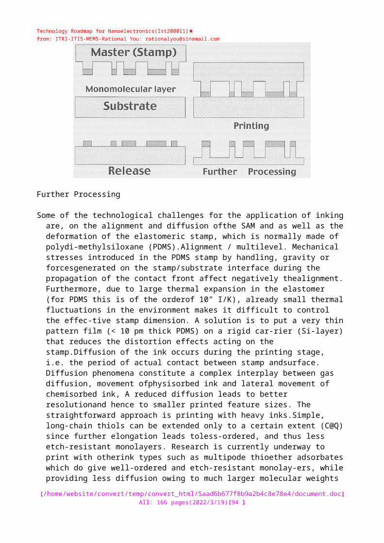
Technology Roadmap for Nanoelectronics(Ist200011)★from: ITRI-ITIS-MEMS-: [email protected]
(@ 56 GHz 55 GHz 1.24THz 150 GHz - 200 M@. .. . S". . 420 mS/
mm233 mS/
mm60 mS/
mmGain, P 1 <lPower
dissipation@>Vd<i
30 mWper gate
- 2 OpW Excludingcooling
Power-delayproduct
Minimum NoiseFigure @2GHz
No. of electrons 100-1000 <100
Table 19: Forecast Logic I High Frequency Devices Yar 2006
Technology SiGe n-MODFET
SiGe p-MODFET
InAsRTD SET logic Molecular
Lithography 100 nm 100 nm 200 nm 100 nm 100 nmFeature size 70 nm 70 nm 2 nm 10 nm 5 nmSwitching
time(gate delay perstage)
200fs 500ns 1 ns
f. 150 GHz 70 GHz ITHz - MHz 500 MHzt max 1 THzR@ 950mS/mm 237mS/mmGain, p 1 -1Power
dissipation @>Vu
10s nW ILlW 10 pWexcluding cooling
-1 RLW
Power-delay product
200aJ -laJ lfl
Minimum No iseFigure @2GHz
No. ofelectrons lOGOs 1000s <100 <100
Table 20: Forecast Logic I High Frequency Devices Year 2012Technology SiGe n-
MODFETSiGe p-
MODFETInAsRTD SETlogic Molecular
Lithography 50 nm 50 nm - lOOnm 50 nm 50 nmFeatlire size 30 nm 30 nm @2 nm < 10 nm < 5nmSwitching time
(gatedelay per stage)
3ps 5ps 200 fs 100ns 10ns
FT 320 GHz 200 GHz lTHz -10 MHz -100 MHz
【/tt/file_convert/5aad6b677f8b9a2b4c8e78e4/document.doc】All: 107 pages(2023/5/6)【94 】
Technology Roadmap for Nanoelectronics(Ist200011)★from: ITRI-ITIS-MEMS-: [email protected]
F@,@ ITHzG@ > 1000 mS/mm - 800 mS/ mmGain, pPower
dissipation @ Vdd
-1 - 1
30 tlW 20 nW -lpW InWPower-delay
product100 aJ 100 aJ -lOaT 10 aT
Minimum Noise Figure@>2GHi
No. of electrons 500 500 <20 <10
Table 21: Comparison Circuit Performance Year 2000
Technology CMOS lnAsRTD/ HFET
RSFQLTS RSFQHTS QCA SET logic Molecular
Reference [104] [134] [5] [215] NodemoFeature size 180 nm 100
nmHFETIxl nmRTD
3500 nm 2000 nm 2000 nm
10 nm (200nmlith)
No. of active elements(a)
110 M @ 50MIO(@ 510> 8 ln3 10
Circuit Speed
1.25 GHz 2 GHz M35GHz@
IGHz 170 GHz IHz IMHz
Events / chip / s
1.3810'7 0.810'@ @3.510'@ @
1012 M 610'@M 1 107
Power supply, Vdd
1.8V 0.7V N/A 0.1V
Power dissipation
90Wtot.jchip
21fr3Wpergate
10-3 W'''Wntdchip
IO-i-WIdMItotalchip
N20 n 10-" Wper gate
Temperature
400 K 300 K 4K 40 K 0.075 K
4K
Table 22: Forecast Circuit Performance Year 2006Tecliilology CMOS SiGe
HCMOS
InAsRTD/HFET(>20to/ cm')
RSFQNb RSFQHTS(k) QCA SET logic
Feature size 65 nm 70 nm 80 nmHFET200x200 1000 nm 1000 nm 30 nm lOOnm
【/tt/file_convert/5aad6b677f8b9a2b4c8e78e4/document.doc】All: 107 pages(2023/5/6)【95 】
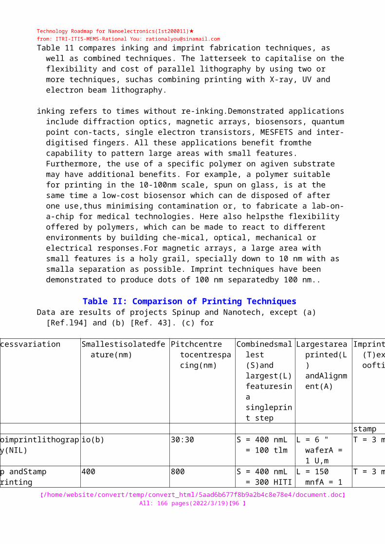
Technology Roadmap for Nanoelectronics(Ist200011)★from: ITRI-ITIS-MEMS-: [email protected]
nroRTD
No. of activeelements M
8.810@ 2 Iff 10 @> 10" 103 4 100
Circuit Speed 3.5 GHz 5.25 GHz
6 GHz l-l 50 GHz @l 100 GHz 200 GHz -lkHe 5 MHz
Events / chip /s 3.110'@ 1.0510'@
6 10@ M 5 10"> @) 10@ 410" 4 Iff 510"
Power supply,Vdd
1.8V 0.5V 0.6V O.I mV lmV
Powerdissipation 150 Wtotalchip
80W 2 10 -I W per gate 510-3WM@rotalchip
510@@W@)('@)tot,@lchip
410"W@per gate
<lnW
Temperature 400 K 400 K 300 K 4K 40 K 20 K 77 K
Table 23: Forecast Circuit Performance Year 2012
Technology CMOS SiGeHCMOS InAsRTD/HFET(> 40kA/ cm@
RSFQMb RSFQHTS QCA SETlogic Mole-cular
Feature size 30 nm 30 nm 50 nm HFET50 x50 nrn@ RTD
500 nm 500 nm (m) 2 nm(50nm lith)
- 2 nm
No. of activeelements
7.110" 4.6810" 10" 105 l@ 107 10'@
Circuit Speed 10 GHz 15 GHz 24 GHz Id 60 GHz(D
200 GHz 350 GHz 10 MHz - 1 MHz
Events / chip/s 7.110 @" 710'" 2.4 10'" M 6.0 10"@IB
10 '<@ 10@ IO'" 10'"
Power supply,@Vu
0.5V 0.5V 0.5V 0.1V IV@
Powerdissipation 174Wrotalchip 17.5 Wtotalchip
10-3W per gate 10W total chip
5 W"MM)iotalchip
510'l <dM)totalchip
<lnWMper gate
108 WM
Temperature 400 K 400 K 300 K 4K 50 K 77 K 300 K
【/tt/file_convert/5aad6b677f8b9a2b4c8e78e4/document.doc】All: 107 pages(2023/5/6)【96 】
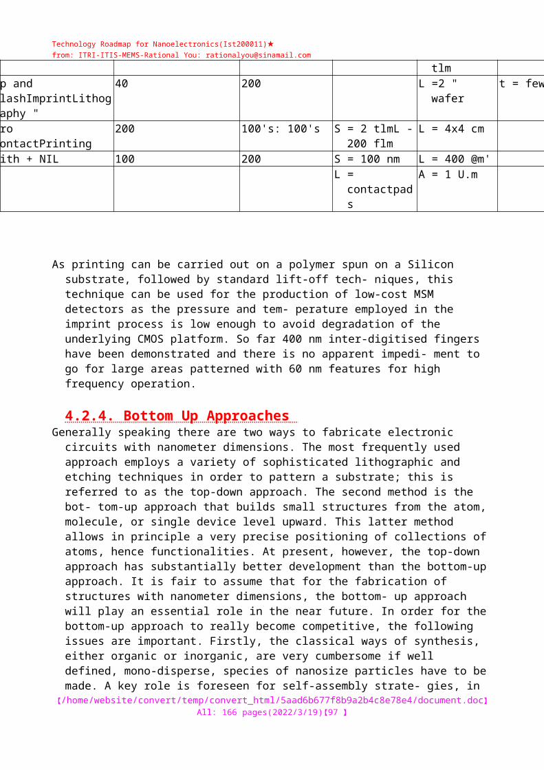
Technology Roadmap for Nanoelectronics(Ist200011)★from: ITRI-ITIS-MEMS-: [email protected]
8. Annex 8.1. Glossary Analogue Digital Converter Arithmetic Logic Unit Anisotropic magneto resistance Artificial
Neural Networks Array Processors Application Specific Integrated Circuits Binary Decision Diagramme Complementary Metal Oxide Semiconductor Cellular Neural Networks Computing: Deoxyribo Nucleic Acid Dynamic RAM Digital signal processors Erasable programmable read only memories Electron Spin Resonance Extreme Ultraviolet (lithography) Field Effect Transistor Future and Emerging Technology (branch of the Commissions 1ST Programme) Field Programmable Gate Arrays Giant magneto resistance Highest occupied molecular orbitalHigh Temperature SuperconductorsIntelligent RAMInformation Society Technology (Programme)Interband Tunnelling DeviceInternational Technology Roadmap for SemiconductorsLow Temperarture SuperconductorsLowest unoccupied molecular orbitalMicroELectronics Advanced Research Initiativemillions of instructions per second = clock frequency (MHz) x instructions per clock. This value gives a measure for the performance of logic circuitsMonostable-bistable transition logic elementmetal oxide semiconductor field effect transistorMagnetic RAMNanotechnology Information Devices (a initiative of the FET section of theCommission's 1ST programmeNuclear Magnetic ResonanceNon Volatile RAMPropragate Instruction ProcessorQuantum ComputingQuantum Cellular AutomatonQuantum Information ProcessingRandom Access Memory
RAWRISCRSFQRTDSETSIASIMDSRAMVLIWVRTT
Reconfigurable Architecture WorkstationReduced Instruction Set Complexity (Processor)Rapid Single Flux Quantum (Logic)Resonant Tunnelling DeviceSingle Electron Tunnelling (Device)Semiconductor Industry AssociationSingle Instruction Multiple Data (architecture)Static RAMVery Long Instruction Word (architecture)Vertical resonant tunnelling transistors
8.2. Research Projects The groups of the following research projects have contributed to this document. Abstracts of the
projectsand the list of the participating groups can be found at the
NID homepage http,'//www.cordis.lu/ist/fetnid.htm
CHARGE LASMEDS SIQUIC FASEMNANOWIRESQUESTSPIDERQUADRANTRSFQ-HTSLOCOMSPINUPNANOTECHANSWERSQ-SWITCHNANOMEMNANOLITHCHANILCORTEXSANEMEBIOANDBUN
The Coulomb Blockade Applied to the Realisation of Electronics Fabrication of elementary Molecular Electronic Devices Silicon Quantum Integrated Circuits Fabrication and Architecture of Single Electron memories Conductance characteristics and mass fabrication of Nanoscale integrated circuit nanowires Quantum Electronics using Scanning Tunnelling microscopy based lithography SPIn Dependent Nano-Electronics Quantum Devices for Advanced Nano-electronic Technology High Temperature Superconducting Rapid Single Flux Quantum Logic Logic Circuits with Reduced Complexity based on Device with Higher FunctionalitySemiconductor Processing by ImpriNt of Ultrasmall PatternsDevelopment of Nanoimprinting Techniques suitable for Ilarge area mass production of nm-scale patternsAutonomous Nanoelectronic Systems With Extended Replication and SignallingHeterostructure defined electron wave guides
【/tt/file_convert/5aad6b677f8b9a2b4c8e78e4/document.doc】All: 107 pages(2023/5/6)【97 】

Technology Roadmap for Nanoelectronics(Ist200011)★from: ITRI-ITIS-MEMS-: [email protected]
for quantum based switching applica-tions.Semiconductor free nanoscale non-volatile electronics and memories based on mag-netic tunnel junctionsArrays of microguns for parallel e-beam nanolithographyNanoimprint based fabrication of charge sensing devices for information processingDesign and construction of elements of hybride molecular /electronic retina cortex structureself assembly of functional nanscale elements for intra-molecular electronicsBiomolecule driven assembly of nanoparticle based electronic devicesBottom-up Nanomachines
DNA-BASED ELECTRONICS
SATURNNANOMOLNANOMASSNANOTCADNICEATOMSFRACTUREDEW
Self Assembly with nanotubes: towards devices for information processingManufacturing and modelling of nano-scale molecular electronic devicesNanoresonators with integrated circuitry for high sensitivity and high spacial resolu-tion mass detectionNanotechnology Computer Added DesignNanoscale Integrated Circuits using Endohedral fullerenesAssembler tool for molecular structuresNanoelectronic devices and fault-tolerant architecturesDouble Electron Waveguides
8.3. Contributors The following persons haveAhopelto, J.Bachmann, G.Brillouet, M.Briinger, W.Compano, R.de
Boeck Jo,Debray, Ph.Dubois, E.Forshaw, M.Forster, A.Fountain, T.Garcia, R.Gimzewski, J.K.Gippius, N.GIezos.N.Greer, J.Hadley.P.Haviland, D.Humphreys, R.Huskens, J.lannaccone, G.Joachim, Ch.Kaesmaier, R.Kelly, M.Kern.D.Launois, H.Lindelof, P.Macucci, M.Mahler, G.Malindretos, J.Martorell, J.Mengel, S.Molenkamp, L.Montelius, L..Morales, P.Mueller, H.-O.Niemeyer, J.Pacha, Ch.Paul, D.Prost, W.Samuelson, L.Sazio, P.
particularly contributed to the first or the second edition of this document: VTT Espoo, Finland VDI Diisseldorf, Germany Leti Crolles, France Fraunhofer Institut, Berlin, Germany European Commission (DG Infso), Brussels, Belgium IMEC, Belgium CEA Saclay, France ISEM Lille, France University College London, UK ISI FZ Jtilich, Germany University College London, UK Centre Nacional de Microelectronia, Madrid, Spain IBM Zurich Laboratories, Switzerland Universitaet Wuerzburg, Germany IMEL Demokritos, Greece NMRC Cork, Ireland Technical University of Delft, Netherlands KTH, Sweden DERA, UK University ofTwente, Netherlands University of Pisa, Italy CNRS Cemes, Toulouse, France Infenion, Miinchen, Germany University of Surrey, U.K. Tilbingen University, Germany L2M, CNRS, Paris, France University of Copenhagen, Denmark University of Pisa, Italy University of Stuttgart, Germany ISI FZ Jiilich, Germany University of Barcelona, Spain VDI Diisseldorf, Germany University Wiirzburg, Germany University Lund, Sweden ENEA, Italy Hitachi Cambridge Laboratory, UK Physikalisch Technische Bundesanstalt, Germany Infenion AG Miinchen, Germany University of Cambridge, U.K. University of Duisburg, Germany University of Lund, Sweden University of Cambridge, UK
Schenk, A.Schmidt, G.Sotomayor, C.Sprung, D. W. L.Stockbro, K.Van Rossum, M.Vu Thien Bihn,Welland, M.Yakimenko, 1.
ETH Zurich, SwitzerlandUniversity ofWurzburg, GermanyUniversity ofWuppertal, GermanyMcMaster University, CanadaMIC Technical University of Denmark, DenmarkIMEC Leuven, BelgiumUniversity of Lyon I - CNRC, FranceUniversity of Cambridge, U.K.University
【/tt/file_convert/5aad6b677f8b9a2b4c8e78e4/document.doc】All: 107 pages(2023/5/6)【98 】

Technology Roadmap for Nanoelectronics(Ist200011)★from: ITRI-ITIS-MEMS-: [email protected]
of Linkoeping, Sweden
8.4. References 1.Adieman L. "Molecular computation of solutions to combinatorial problems" Science 266, pp
1021- 1024 (1994)2.Aharonov Y., and D. Bohm "Significance of electromagnetic potentials in the quantum theory" Phys. Rev. 115, pp. 485 (1959)3.Ahopelto J., M. Prunnila, S. Eranen, M. Kamp, M. Emmerling, A. Forchel, A. Kristensen, P.E. Lindelof, and A, Gustafsson "Quantized conductance in narrow-channel SOI MOSFETs" Electrochem.Soc. Proc. 99-22, pp. 348 (1999)4. Akazawa M., "Binary-decision-diagram logic systems using single-electron circuits and single-flux- quantum circuits" preprint 1998 (akazawa@sapiens-ei,eng,hojudai.ac.jp)5.Amiani 1., A. 0. Orlov, G. Toth, G. H. Bernstein, C. S. Lent, G. L. Snider, Science, v. 284, 289 (1999).6.Amiani, A. 0. Orlov, G. L. Snider, C. S. Lent, and G. H. Bernstein, Appl.Phys. Lett. 72, 2179 (1998)7.Ancona M.G, "Bit errors in single-electron digital circuits", Proc. Int. Workshop on Quantum Functional Devices, NIST GaithersburgVA, Nov (1997)8. Ancona M.G, "Systolic processor design using single electron digital circuits", Superlattices and Microstructures, 20(4) pp. 461-471 (1996)9.Ancona, M. G.. "Single electron digital circuits: possibilities and problems "Phasdom 97, Aachen 10- 13 March (1997)10. Andes R.P, T. Bein, M. Dorogi, S. Feng, J.I. Henderson, C.P. Kubiak, W Mahoney, R.G. Osifchin and R. Reifenberger, "Coulomb staircase at room temperature in a self-assembled molecular nanos- tructure" Science 272, ppl323-1325 (1996)11. Asai S and Y. Wada, "Technology challenges for integration near and below O.lpm", Proc. IEEE, 85, pp505-520 (1997)12. A@hwell G.J, J.R. Sambles, A-S. Martin, W.G, Parker and M. Szablewski, J. Chem.Soc. Chem, Commun. 1374 (1990)13. Aviram A. "Molecules for memory, logic and amplification" J. Am. Chem. Soc. 110, 5687 (1988)14. Aviram and M.A. Ratner, "Molecular rectifiers" Chem. Phys. Lett. 29 277 (1974)15. Aviram, J. Am. Chem. Soc. 110, 5687 (1988)16. Bachmann G., VDI-TZ Diisseldorf, Germany, private communication17. Bachmann. G. "Innovationsschub aus dem Nanokosmos", VDI-TZ Diisseldorf, Germany, October 199818. Ball Ph. "Meet the spin doctors..." Nature 404, 918 (2000)19. Behr, "The Lock and Key Principle" John Wiley and Sons, (1994)20. Bernstein K., K. M. Carrig, Ch. M. Durham, P. R. Hansen, D. Hogenmiller, E.J. Nowak, N. J. Rohrer, "High Speed CMOS Design Styles", Kluwer Academic Publishers, 1998.21. Berzon D. &T.J. Fountain, "A memory design in QCAs using the SQUARES formalism", 9th Great Lakes Symposium on VLSI, March (1999) IEEE, p. 166, Eds. R.J. Lomax, P. Mazurnder22. Biebuyck H.A et al., "IBM J. Res. Develop". 41 , page 159 (1997)23. Birge R.R. and R.B. Goss "Biomolecular optoelectronics" in "Introduction to Molecular Electron- ics" Edited by M.C. Petty, M.R. Bryce and D. Bloor, Edward Arnold, London, (1995) 24. Birge R.R., Annual Review Phys. Chem. 41, pp683-733 (1990) 25. Boeve H., B. Dutta, J. De Boeck, G. Borghs, R. Van De Veerdonck, R. Coehoorn, J.S. Moodera, to be published.
26. Borkar S., "Technolog/Trends and Design Challenges for Microprocessor Design", Proc. of the 24th European Solid-State Circuits Conference, The Hague, The Netherlands, 22-24 Sept, pp. 7-8 (1998) 27. Boxer S.G., J. Stocker, S. Franzen and J. Salafsky in "Molecular Electronics- Science and Technology" Eds. A. Aviram (Am. Inst. Phys., New York, 1992)28. Brandbyge M., Stokbro K., MIC-Technical University of Denmark 29. Braun E., Y. Eichen, U. Sivan and G. Ben-Yoseph, "DNA-templated assembly and electrode attach- ment of a conducting silver wire" Nature, 391, pp775-778 (1998)30. Broekaert T. P. E., J. N. Randall, E. A. Beam III, D. Jovanovic, A. C. Seabaugh, and B. D. Smith "Functional InP/InGaAs lateral double barrier heterostructure resonant tunneling diodes by using etch and regrowth", Appl. Phys. Lett. 69,
【/tt/file_convert/5aad6b677f8b9a2b4c8e78e4/document.doc】All: 107 pages(2023/5/6)【99 】

Technology Roadmap for Nanoelectronics(Ist200011)★from: ITRI-ITIS-MEMS-: [email protected]
1918 (1996)31. Broekaert T.P.E., B. Brar, J.P.A. van derWagt, A.C. Seabaugh, EJ. Morris, T.S. Moise, E.A. Beam III and G.A. Frazier, "A monolithic 4-bit 2Gsps resonant tunnelling analogue-to-digital converter" IEEE J. Solid-State Circuits 33,A ppl342-1348 (1998)32. Broekart T.P.E., B. Brar, F. Morris, A.C. Seabaugh & G. Frazier, "Resonant tunneling technology for mixed signal and digital circuits in the multi-GHz domain", 9th Great Lakes Symposium on VLSI, March 4-6,1999, Ann Arbor Michigan,?. 123 Eds. R.J. Lomax, P. Mazurnder33. Brown J. and A. Pohm'l-Mb Memory Chip Using Giant Magnetoresistive Memory Cells", IEEE Trans on Comp, Pack and Manufact Techn. A, 17(3), pp-373 (1994)34. Bruenger W.H., et al. "Resolution Improvement of Ion Projector with a LowEnergy Spread Multicusp Ion Source", MNE 98, Leuven, to be published in Microelectron. Eng. (1999) L.A. Bumm et al. Science 271, 1705 (1996)35. Burleson W.P., M. Ciesielski, F. Klass & W. Lu, "Wave-pipelining: a tutorial and research survey", IEEE Trans. VLSI Syst. 6, 464-473, (1998)36. Canning}. '"International SEMATECH Lithography activities" Presentation at XEL (1998)37. Canning}. "Potential and challenges for lithography beyond 193 nm optics" J.Vac. Sci. Technol. Bl$, pp2109-2111 (1997)-38. Chen K.J., K. Maezawa, M. Yamamoto, "InP-Based High Performance Monostable-Bistable Transition Logic Elements (MOBILE'S) Using Integrated Multiple-Input Resonant Tunneling Device". IEEE Electron Device Letters, 17(3), pp-127-129. Mar. (1996)39. Chen L., RH. Mathews, L.J.Mahoney, PA. Maki, K.M. Molvar, J.P. Sage, G.L Fitch, T.C.L.G. Sollner. "New Self-Aligned Planar Resonant-Tunnelling Diodes for Monolithic Circuits". IEEE Electron Device Lett., Vol. 18 No. 10, October 1997, pp. 489-491.40. Chen T. (ed) "Highlights of statistical signal and array processing", IEEE Signal Proc. Mag. September 1998, pp 21-63.41. Cholet S., Joachim C., Martinez J.P, Rousset B., "Fabrication of co-planar metall-insulator-metal nanojunction down to 5nm" Europhys. J. AP 8, 139 (1999)42. Chou S.Y. and PR. Krauss,"lmprint lithography with sub-IOnm feature size and high through- put",Phasdom 97, Aachen 10-13 March (1997)43. Chou S.Y, P R Krauss, W Zhang, L Gua and L Zhuang, J Vac Sci Technol B 15 (6) (1997)44. Cowburn R. P., M. E. Welland, Science, v. 287, 1466 (2000).45. Crawley D., "An analysis of MIMD processor node designs for nanoelectronic systems", UCL IPG Report 97/3, available via http://ipga.phys.ucl.ac.uk/reports/html46. Cressler J.D. "SiGe HBT technology: a new contender for Si-based rfand microwave circuit applica- tions" IEEE Trans. Microwave Theory Techniques 46 ,pp572-589 (1998)47. Cuberes M.T.,R.R. Schlittler and J.K. Gimzewski, "Room temperature supramolecular repositioning
at molecular interfaces using scanning tunnelling microscope", Surface Sci. Lett. 371, ppL231-L234 (1997)48. Cuberes M.T., R.R. Schlittler and J.K. Gimzewski, "Room temperature repositioning of individual C60 molecules at Cu steps: operation of a molecular counting device" Appl. Phys. Lett. 69, pp3016- 3018 (1997); see also http://www.zurich.ibm.com/News/Abacus49. De BoeckJ., G. Borghs, Physics World pp. 27 - 32 (April 1999)50. Debray P., V. N. Zverev, M. Rahman, E. Strobel, E. Kohn, and B.Vinter, "A Novel Nanometer Ballistic Quantum Device for Potential Use in Analog-to-Digital Conversion", Seventeenth Biennal lEEE/Cornell University Conference on Advanced Concepts in High Performance Devices, August 7-9, 2000, Cornell University, lthaca, USA.51. Di Ventra M., S.T. Pantelides and N.D. Lang, Appl. Phys. Letters 76, 3448 (2000).52. Diers, J.R. M.R.De Armond, J. Guay, A. Diaz, W. Rulian, J.S. Schumm, J.M. Tour "ESR character- isation ofoligomeric thiophene materials", Chem. Mater. 6, 327 (1994)53. Died T. et al. Science 287, 1019 (2000)54. Dracopoulos T., Evolutionary learning Algorithms for Neural Adaptive Control, Springer-Verlag (1997)55. Durrani Z.A.K., A.C. Irvine., H. Ahmed, K. Nakazato, "A memory cell with single electron an metal oxide semiconductor transistor integration, Applied Physics Letters 74, 1293 (1999)56. Duschi R., 0. G. Schmidt, and K. Eberi, "Epitaxially grown Si/SiGe interband
【/tt/file_convert/5aad6b677f8b9a2b4c8e78e4/document.doc】All: 107 pages(2023/5/6)【100 】

Technology Roadmap for Nanoelectronics(Ist200011)★from: ITRI-ITIS-MEMS-: [email protected]
tunneling diodes with high room-temperature peak-to-valley ratio". Applied Physics Letters, Vol. 76(7), pp. 879-881 (2000).57. Esaki L., Phys. Rev. 109, 603 (1958).58. European Commission, 1ST programme "Technology roadmap, Optoelectronic interconnects for integrated circuits". Second Edition: September 1999 ISBN 92-828-7762-059. Evers N. et al..lEEE Electron Dev. Lett. 17, p443 (1996)60. Feldheim L. & C.D. Keating, "Self-assembly of single electron transistors and related devices", Chem. Soc. Rev. 27, ppl-12, (1998)61. Fiederling R., M. Keim, G. Reuscher, W. Ossau, G. Schmidt, A. Waag, L.W. Molenkamp "Injection and detection of a spin-polarized current in a light emitting diode". Nature 402, 787 (1999)62. Fogel D.B. (ed), 'Evolutionary Computation: The Fossil Record', IEEE Press, (1998) (ISBN 0- 7803- 3481-7)63. Fountain T.J., D.G.Crawley, M.R-B.Forshaw, S.Spagocci, D.Berzon, "Novel processor arrays for nanoelectronics". Ultra electronics program review, Estes Park, Colorado, 18-21 Oct. 1998, Digest p.34-38. (1998b)64. Fountain T.J., M.J.B. Duff, D.G. Crawley, C.D. Tomlinson, and C.D. Moffat, "The use of nano- electronic devices in highly parallel computing systems" IEEE Trans. On Very Large Scale Integrated Systems, 6, 31-38, March (1998a)65. Fountain T.J@ Parallel Computing: Principles and Practice, Cambridge University Press, (1994)66. FPGA-based Computing Machines website (1998): http://www.io.com/-guccione/HW-list.html67. Fujiwara A et al., 'Silicon double-island single-electron device', pp 163-167, Technical Digest, Int. Electron Devices Meeting (IEDM97), IEEE Inc., 445 Hoes Lane, Piscataway NJ 08855, USA, (1997)68. GallagherW.J. et al. "Microstructured magnetic tunnel junctions", J. Appl, Phys. 81, 3741 (1997)69. Galvin R,, "Science Roadmaps" Science 280, 803 (1998)70. Geddes, N.J., Sambles J.R., Davis D.J., Parker W.G,, Sandman D.J. "Fabrication and investigation of
asymmetric current-voltage characteristics of a metal/Langmuir-Blodgett monolayer/metal structure", Appl. Phys. Lett. 56, 1916 (1990)71. Gimzewski Joachim and J.K. "An electromechanical amplifier using a single molecule" Chem. Phys. Lett. 265, pp353-357 (1997), see also http://www.zurich.ibm.com/72. Girlanda M., M. Governale, M. Macucci, and G. lannaccone, Appl. Phys. Lett., v. 75, 3198 (1999).73. Goldhaber-Gordon D., M.S. Montemerlo, J. C. Love, G.J. Opiteck and J.C. Ellenbogen, "Overview ofnanoelectronic devices" Proc. IEEE 85, pp521-540 (1997)74. Goser K., C.Pacha, A.Kanstein, and M.L.Rossmann "Aspects of systems and circuits for nanoelec- tronics" Proc. of the IEEE, 85, 558-573, April (1997)75. Gossens M.J., "Analog Neural Networks in Single Electron Tunneling Technology", Ph.D Thesis, TU Delft, The Netherlands, (1998)76. Governale M., M. Macucci, G. lannaccone, C. Ungarelli, J. Martorell, J. Appl. Phys. vol. 85, 2962 (1999).77, Granly and Hurst, Presented at the 1996 Int'l NonVoladle Memory Technology Conference (IEEE) Digest pp.l38 (1996)78. Greenbaum E., J. Phys. Chem. 96, pp5l4-5l6 (1992)79. Greer J.C., S. lhara and T. Vrotsos, eds, "Ab initio approaches to microelectronics materials and process modelling", 3 (2000) Special issue of Materials Science in Semiconductor Processing.80. Gronowski P.E., W.J. Bowhill, R.P. Preston, M.k. Gowan &: R.L. Allmon,'" High-performance microsprocessor design", lEEEJourn. Solid-State Circ-33, 676-686, (1998)81. Gwyn C.W., R.@Stulen, D. Sweeney, and D. Attwood "Extreme ultraviolet lithography" J. Vac.Sci.Technol. B16,3142 (1998)82. Haatainen T, P Majander and J Ahopelto, presented at the 6th MELARI/NID Workshop, 25-28 June, Enschede, The Netherlands83. Haatainen T, P Majander and J Ahopelto, Proc SPIEs 25th Int. Symp. Microlithography: Emerging Lithographic Technologies III, 28 February - 3 March 2000, Santa Clara, California, USA.84. Hadley P. & J.E. Mooij, "Quantum nanocircuits: chips of the future?", TU Delft reprint, (1999) (http://vortex.tn.delft.nl/-hadley/publications/qdevices99/pearsal.html)85. Hadley P., E.H. Visscher, Y. Chen and J.E. Mooij, "An offset charge independent single electronics RS flip flop" Proc. International Conference on Quantum Devices and Circuits, p224, Alexandia, Egypt, June
【/tt/file_convert/5aad6b677f8b9a2b4c8e78e4/document.doc】All: 107 pages(2023/5/6)【101 】
Technology Roadmap for Nanoelectronics(Ist200011)★from: ITRI-ITIS-MEMS-: [email protected]
4-7, (1996)86. Hagele D., et al. Appl. Phys. Lett. 73, 1580 (1998))87. Hall L.E., J.R. Reimers, N.S. Hush and K. Silverbrook, Journal of Chemical Physics, v. 112, 1510 (2000).88. Hameroffet al. Computer 25(11), pp30-39, (1989)89. Hamilton S., "Taking Moore's Law Into the Next Century", IEEE Computer, Jan. 1999, pp. 43-48 (1999)90. Hanafi H. 1., S. Tiwari and 1. Khan, IEEE Trans. Electron Devices 43(9), 1553 (1996)91. Harriot L.R. "Scattering with angular limkitation projection electron beam lithography for sub- opti- cal lithography'J. Vac. Sci. Technol. B15(6, pp2130-2135 (1997)92, Harris D., D, M.A. Horowitz, "Skew-tolerant domino circuits", IEEE Journal of Solid-State Circuits, Vol. 32, No. II, November 1997, pp. 1702-1711.93. Haykin S., Neural Networks, Macmillan, NY, (1994)94. Heath J.R., P.J. Kuekes, G.S. Snider & R-S.Williams, "A defect-tolerant computer architecture: opportunities for nanotechnology",Science 280, ppl7l6-1721, (1998)
95. Heidari B, I Maxirnov, E-L Sarwe and L Montelius, paper presented at the 44th EIPBN conference,May 30-June 2, 2000, Palm Springs, California, USA.6. HennessyJ.L., D.A. Patterson, Computer architecture: a quantitative approach,7. Hillenius S. and W.F. Brinkman "Microelectronics beyond roadmaps" The Future ofMicroelectronics: Off the Beaten Path, lie des Ernbiez, France, June (1998) Hopfield, Nature confer-ence on Nanotechnology, Tokyo, (1992)8. Hou and J.M. Philips. Appl. Phys. Lett. 67, pp286-288 (1995)9. Huang C.K., W.E. Zhang, and C.H. Yang, "Two-Dimensional Numerical Simulation of SchottkyBarrier MOSFET with Channel Length to 10 nm", IEEE Transactions on Electron Devices, Vol. 45,No. 4, April 1998, pp. 842-848.00. Huskens private communication01. INESC, presented at MMM conference02. Ishikuro H. and T. Hiramoto, "Fabrication of Si point contact MOSFETs acting as single electrontransistor at room temperature". Silicon Nanoelectronics Workshop, Kyoto, June 8-9 (1997)03. ltoh K. et al., "Trends in Low-Power RAM Circuit Technologies", Proc. IEEE 84,pp524-543(1995)04. ITRS:-"lnternational Technology Roadmap for Semiconductors", edition 1999. The document canalso be downloaded at the web site: http://www.itrs.net/ntrs/publntrs,nsf05. lwai H., "Future of LSI: Lithography, Interconnects, etc.", The Future of Microelectronics: Off theBeaten Path, lie des Ernbiez, France, June (1998)06. Jeong G.J. and M.K. Lee, "Design of a Scalable Pipelined RAM System", IEEE J.Solid State Circuits33, pp 910-914 (1998)07. Joachim C. , J.K. Gimzewski, H. Tang "Physical Principles of the single C60 transistor effect" Phys.Rev. B5816407 (1998).08. Joachim, C., J.K. Gimzewski, A. Aviram "From molecular to monomolecular electronics" Nature(2000)09. Jou S.J., C.Y, Chen, E.G. Yang, and C.C. Su, "A Pipelined Multiplier-Accumulator Using a HighSpeed Low Power Static and Dynamic Full Adder Design", IEEE J. Solid State Circuits 32, pp. 114-118(1997)10. JungTA., R.R. Schlittler and J.K. Gimzewski, "Conformarional identification of individual adsorbedmolecules with the STM", Nature 386, pp696-698 (1997)11. Kane B.E., "A silicon-based nuclear spin quantum computer". Nature 393, 133-137, (1998)12. Kasper E. (1998) in addition to S. Luryi et al. lEEETrans. Elec. Dev. ED31, 832 (1984)13. Kawaura H., T. Sakamoto, T. Baba, Y. Ochiai, J. Fujita, S. Matsui and J. Sone, "Transistor operationof30nm gate-length EJ-MOSFETs", IEEE Elec. Dev. Lett. 19, pp74-76 (1998)14. KikkawaJ. et al. Science 277, 1284 (1997), Science 281, 656 (1998), Nature 397 (1999), Physics Today P33 (June 1999),15. Kikkawa J.M., D.D Awschalom."Resonant spin amplification in n-type GaAs," Phys. Rev. Lett. 80, 4313-4316 (1998)16. Klimeck G. et al., "Design and Implementation of Resonant Tunnelling Devices into Circuits and Applications", Phasdom 97, Aachen, Germany, March (1997)17. Kohonen, "Self-organising maps", Springer-Verlag, Berlin, (1995)18. Koren & Z. Koren, "Defect tolerance in VLSI circuits: techniques and yield analysis", Proc. IEEE 86,1819-1836, (1998)19.Korkin M., H.de Garis, F. Gers & H. Hemmi, "CBM (CAM-BRAIN MACHINE,http://www.genobyte.com/GP97full.html
【/tt/file_convert/5aad6b677f8b9a2b4c8e78e4/document.doc】All: 107 pages(2023/5/6)【102 】
Technology Roadmap for Nanoelectronics(Ist200011)★from: ITRI-ITIS-MEMS-: [email protected]
120. Koronkov, Chen and Likharev, J. Appl. Phys. 78, pp2520-2530 (1995) 121. Kozyrakis C.E., D.A.Patterson. A new direction for computer architecture research, IEEE Computer,31,24-32, Nov.(1998) 122. Kristensen A, J.B. Jensen, M. Zaffalon, C.B. Serensen, S.M. Reimann, P.E. Lindelof, M. Michel, andA. Forchel "Conductance quantization above 30 K in GaAlAs shallow-etched quantum point contactssmoothly joined to the background 2DEG"J. Appl. Phys. 83, pp. 607 (1998) 123. Kristensen A., H. Bruus, A.E. Hansen, P.E. Lindelof, J. Nygard, C.B. Serensen, and A. Forchel "Biasand temperature dependence of the 0.7 conductance anomaly in quantum point contacts" cond-mat/0005082 (2000) 124. Kurihara K@ H. Namatsu, M. Nagase and Y. Takahashi "Fabrication and process for room tempera-ture operated single electron transistor using electron beam nanolithography", SiliconNanoelectronics Workshop, Kyoto, June 8-9 (1997) 125. Kusunoki T., K. Yamaguchi and N. Homma, "A 1.8 ns access, 550 MHz, 4.5 Mb CMOS SRAM"IEEEJ. Solid State Circuits 33, ppl650-l658 (1998) 126. Lang N.D and Ph. Avouris, Phys. Rev. Lett. 81, 3515 (1998). 127. Lebedev D et al, presented at the 5th MELARI/NID Workshop, 23-26 February, Pisa, Italy 128. Lehn "Supramolecular Chemistry: Concepts and Perspectives" VCH, Weinheim, (1995) 129. Lent C.S. and P.D. Tougaw "A device architecture for computing with quantum dots" Proc. IEEE 85, pp54l-557 (1997) 130. Lent S., "Quantum Computation and its perspective," A report to the Research and Development Association for Future Electron Devices, FED Journal, April 1997 131. Liebau M, Y Chen, A Lebib, J Husken and D N Reinhoudt, presented at the 6th MELARI/NID Workshop, 25-28 June, Enschede, The Netherlands. 132. Likharev K.K., Nanotechnology 10, 159 (1999) 133. Likharev K.K., Private Communication, (1997)134. LOCOM (NID project No 28844), W.Prost, U-Auer, C.Pacha, G.Jannssen, J. Malindretos, T.G. van den Roer, F.-J.Tegude, K,F.Goser and: Manufacturability and Robust Design ofNanoelectronic Logic Circuits based on Resonant Tunnelling Diodes, W. Prost, U. Auer, F.-J. Tegude, C. Pacha, K.F, Goser, G. Janfien, T. van der Roer, Journal on Circuit Theory and Applications: Special Issue on Nanoelectronic Circuits, invited paper, April 2000.135. Lugli, P., A. Di Carlo, A. Reale, J. of Phys. - Cond. Matt. II, 6035 (1999).136. Mange D., M. Sipper, A. Stauffer, and G. Tempesti, "Towards Robust Integrated Circuits: The Embryonics Approach", Proceedings of the IEEE, Vol. 88, No. 4, April 2000.137. Mange, E. Sanchez, A. Stauffer, G. Tempesti, P. Marchal &: C. Piguet, "Embryonic: a new method- ology for designing field-programmable gate arrays with self-repair and self-replicating properties", IEEE Trans. VLSI Syst. 6, 387-399, (1998)138. Manoharan H.G., C.P. Lutz, D.M, Eigler "Quantum mirages formed by coherent projection of elec- tronic structure" Nature 403, 512 (2000)139. Matzke, "Will physical scalability sabotage performance gains?", IEEE Computer 30, 4, 37-39, (1997)140. Mazurnder P., S. Kulkarni, B. Bhattacharya, J.P. Sun, and G.I, Haddad, "Digital Circuit Applications of Resonant Tunneling Devices", IEEE Proc. 86, pp 664-686(1998)141.Melngailis J., A.A. Mondelli, 1.L. Berry III and R. Mohondro," A Review of Ion Projection Lithography", J. Vac. Sci. Technol. B16(3) pp927-957 (1998)142. Melo L., L. Rodrigues and P.Freitas "Novel Spin-Valve Memory Architecture"
43. Mengel S. "Statusseminar Magnetoelektronik", VDI-TZ Diisseldorf, Germany, Juni 200044. Metzger R.M., B. Chen, U. Hopfner, M.V. Lakshmikantham, D. Vuillaume, T. Kawai, Wu X.L., H.Tachibana, T.V. Hughes, H, Sakurai, J.W. Baldwin, C. Hosch, M.P Cava, L. Brehmer, G.J. Ashwell"Unimolecular electrical rectification in hexadecylquinolinium tricyanoquinodimethanide" J. Amer.Chem. Soc. 119 ,ppl0455-10466 (1997).45. Microresist. For specifications of the mr-l-8000 and mr-l-9000 polymer families, see MRT GmbHhome page at www.microresist.de.46. Minne S.C, S.R. Manalis, G. Yaralioglu, A. Atalar and C.F. Quate,"lncreasing the Throughput of theAtomic Force Microscope", Phasdom 97, Aachen 10-13
【/tt/file_convert/5aad6b677f8b9a2b4c8e78e4/document.doc】All: 107 pages(2023/5/6)【103 】
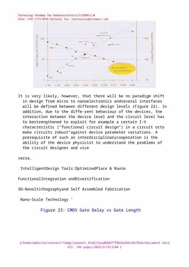
Technology Roadmap for Nanoelectronics(Ist200011)★from: ITRI-ITIS-MEMS-: [email protected]
March (1997)47. Mirkin C.A., R.L. Letsinger, R.C. Mucic and J.J. Storhoff, "A DNA-based method for rationallyassembling nanoparticles into macroscopic materials" Nature 382, pp607-609 (1996)48. Mizuta H. and T. Tanoue "The Physics and Applications of Resonant Tunnelling Diodes" CUP(1995)49. Montelius L, B Meidari, M Graczyk, E-L Sarwe, T G Ling, Proceedings of the Micro and NanoEngineering Conference 1999 (MNE'99), Rome50. Moon J. S., J. A. Simmons, M. A. Blount, J. L. Reno, and M. J. Hafich, "Unipolar complementarycircuits using double electron layer tunneling transistors", Applied Physics Letters, January II, 1999,Vol. 74, Issue 2, pp. 314-316.51. Morgan Kaufman, San Mateo, Cal, USA, (1990)52. Morpurgo A.F., Marcus C.M. Robinson D.B "Controlled fabrication of metallic electronides withatomic separations" Appl. Phys. Lett. 74, 2084 (1999)53. Miiller H-O., K. Katayarna and H. Mizuta "Effects of disorder on the blockade voltage of two-dimen-sional quantum dot arrays" J. Appl, Phys. 84, pp5603-5609 (1998)54. Nakajima et al. Appl. Phys. Lett. 70(13), ppl742-4 (1997)55. Nakamura et al. Nature 398, 786 (1999)56. Nakazato K. et al.. IEDM97 Proceedings (1997)57. Nambu H., K. Kanetani, K. Yamasaki, K. Higeta, M. Usami, Y. Fujimura, K. Ando,58. National Nanotechnology Initiative: Leading to the Next Industrial Revolution, Report by theInteragency Working Group on Nanoscience, Engineering and Technology, Committee onTechnology National Science and Technology Council, Washington, February 200059. Naveh Y. and K.K. Likharev, "Modelling of IO-nm-Scale Ballistic MOSFETs", IEEE Electron DeviceLetters, Vol. 21, No. 5, May 2000, pp. 242-244.60. Ohno Y, D.K. Young, B. Beschoten, F. Matsukara, H. Ohno, D.D. Awschalom "Electrical spin injec-tion in a ferromagnetic semiconductor heterostructure". Nature 402, 790 (1999)61. Orlov 0. et al "Realisation of a Functional Cell for Quantum-Dot Cellular Automata", Science 277,pp 928-930 (1997)62, Pacha C., K.F.Goser, A.Brennemann, W.Prost, "A Threshold Logic Full Adder based on Resonant Tunneling Transisitors", Proc. European Solid State Circuit Conference 1998 (ESSCIRC'98), pp.428-431, Den Haag, NL, September 1998.63. Pacha C., O.Kessler, K. Goser , W. Prost, A. Brennemann, U. Auer, F.J. Tegude, "'Parallel AdderDesign with Reduced Circuit Complexity Using Resonant Tunneling Transistors and ThresholdLogic'", Analog Integrated Circuits and Signal Processing, Special issue on Analog Nano-electronics, July 2000, pp. 5-27.64. Pacha, K. Goser , A. Brennemann, and W. Prost, "A Threshold Logic Full Adder Based on ResonantTunneling Transistors", to be published at ESSCIRC'98, The Hague, NL, September (1998)
65. Pacha, O.Kessler, K. Goser, W. Prost, A. Brennemann, U. Auer, F.J. Tegude,"Parallel Adder Designwith Reduced Circuit Complexity Using Resonant Tunneling Transistors and Threshold Logic", pub-lished in: Analog Integrated Circuits and Signal Processing, Special issue on Circuit Design in Nanoand Quantum Device Technology. (1997)66. Pacha, U. Auer, P. Gloesekoetter, A. Brennemann, W. Prost, F.-J. Tegude & K. Goser, "Resonant tun-neling transistors for threshold logic circuit applications", Proc. of the Great Lakes Symposium onVLSI, March (1999)67. Packan P. A., Science 285, 2079 (1999).68. Palm T. and L. Thylen "Analysis of an electron wave Y-branch switch" Appl.Phys.Lett. 60, pp. 237(1992)69. Patten and S. Wolf (DARPA), Presented at the 1996 Int'l Non-volatile Memory TechnologyConference (IEEE) Digest pp. 1-2 (1996)70. Paul D. et al., final report SiQUIC project No. 22987, 5th MEL-ARI/NID meeting Twente, TheNetherlands, 2000.71. Paul D.J., "Silicon germanium heterostructures in electronics: the present and the future" Thin SolidFilms 321, pp 172-180 (1998)72. Peatman W.C.B., E.R. Brown, M.J. Rooks, P. Maki, W.J. Grimm, M. Shur, "Novel ResonantTunneling Transistor with High Transconductance at Room Temperature", IEEE Electron DeviceLet., Vol. 15, No 7, July 1994, pp. 236-238.73. Pedersen S., A.E. Hansen, A. Kristensen, C.B. Serensen, and P.E. Lindelof "Quantum interferenceabove 4.2 Kin a GaAlAs/GaAs Aharonov-Bohm ring" J. Low Temp. Phys. 118, pp. 457 (2000)74. Pepin A@ C. Vieu, H. Launois, M. Rosmeulen, M. van Rossum, H.O. Mueller, D. Williams, H.Mizuta, and
【/tt/file_convert/5aad6b677f8b9a2b4c8e78e4/document.doc】All: 107 pages(2023/5/6)【104 】

Technology Roadmap for Nanoelectronics(Ist200011)★from: ITRI-ITIS-MEMS-: [email protected]
K. Nakazato, Proceedings of the Micro- and Nano-Engineering '99 conference 21-23September 2000, Rome (Italy)75. Pohm et al, lEEETrans. Magn., 30 (6), pp. 4650 (1994)76. Pohm et al. Presented at the 1996 Int'l Non-volatile Memory Technology Conference ( IEEE) Digestpp.ll3-115 (1996)77. Pohm, J. Daughton, J. Brown and R. Beech "The Architecture of a High Performance Mass Storewith GMR Memory Cells", lEEETrans. on Magn., 31 (6) ,pp.3200 (1995)78. Porter R. et al@ Proc. Fifth Int. Conf. InP and Related Materials, 1993, 37 (1993)79. Quantum Computing: Information about Commission funded projects and activites can be found athttp://www.cordis.lu/ist/fetqipc.htm80. Rabey M., "Digital Integrated Circuits - A Design Perspective", Prentice Hall.Chapter 7 (1996)81. RandallJ.N., Nanotechnology 4, 41 (1993)82. Ranmuthu, K. Ranmuthu, C. Kohl, C. Comstock et M. Hassoun "A 512K-bit Magneto ResistiveMemory with Switched Capacitor Self-Referencing Sensing", lEEETrans on Circuits and Systems-11,39(8), pp.585 (1992)83. Reed M.A., "Molecular electronics - Future Prospects and Reality" The Future of Microelectronics:Off the Beaten Path, lie des Embiez, France, 199884. Reed M.A., C. Zhou, C.J. Muller, T.P. Burgin and J.M. Tour, Science 278, 252 (1997)85. Rommel S.L, T.E. Dillon, PR. Berger, R. Lake, P.E. Thompson, K.D. Hobart, A.C. Seabaugh andD.S. Simons "Si-based interband tunnelling devices for high speed logic and low power memoryapplications" IEDM 98 (1998)86. Sangregorio S., T. Ohm, C. Paulsen, R. Sessoli, D, Gatteschi "Quantum tunnelling of the magneti-zation in an iron cluster nanomagnet" Phys. Rev. Lett. 78, 4645 (1997)
187. Sano K@ K. Murato, T. Otsuji, T. Akeoyoshi, N. Shimmizu, and E. Sano, "80 GBit/s optoelectronic delayed flip-flop circuit using resonant tunnelling diodes and uni-travling photodiode". Electronics Letters 35(16), 1376 (1999).188. Schmidt G. private communication on the Spinup project189. Schubert U. et al, Chimia 51 Nr 7 p 434 (1997)190. Schuiz H, , H-C Scheer, T Hoffmann, C M Sotomayor Torres, K Pfeifier, G Bleidissel, G Gruetzner, Ch Cardinaud, F Gaboriau, M-C Perpignon, J Ahopelto and B Heidari, to appear in J. Vac. Sci. Technol B (2000);191. Schuiz H, D Lebedev, H-C Scheer, K Pfeiffer, G Bleidissel, G Gruetzner and J Ahopelto, , paper pre- sented at the 44th EIPBN conference. May 30-June 2, 2000, Palm Springs, California, USA192. Seabaugh et.al., "Resonant Tunneling Circuit Technology: Has it Arrived?",193. Sessoli R. D. Gatteschi, A. Caneschi, M.A. Novak "Magnetic bistability in a metal-ion cluster" Nature 365,141 (1993)194. Sfil (Step and Flash Imprint Lithography) is being developed by the University of Texas (Austin) and Agilent Technologies. More details at http://www.sfil.org/ and references therein.195. Shorubalko I, P. Ramvall, 1. Maxirnov, H.Q. Xu, W. Seifert, P. Ornling, and L. Samuelson "Coulomb blockade and resonant tunneling in etched and overgrown GalnAs/lnP quantum dots" Appl. Phys, Lett. cm, pp. XXX(2000)196. SilbermanJ et al.,"A I.O-GHz Single-Issue 64-Bit PowerPC Integer Processor, IEEE Journal of Solid- State Circuits, Vol. 33, No. II, November 1998, pp. 1600-1608.197. Silverman J.P. "'Challenges and progress in X-ray lithography" J. Vac. Sci. Technol. B16, 3137 (1998)198. Single C., R. Augke, E E. Prins, D. A. Wharam, D. P. Kern, Semic. Science and Tech. v. 14, 1165 (1999).199. SorefR-A. "Silicon based optoelectronics" Proc. IEEE 81, pp 1687-1706 (1993) A. Steane, "Quantum computing". Rep. Prog. Phys. 61, 117-173, (1998)200. Stock J., J. Malindretos, M. Indlekofer, M. Pottgens, A. Forster, and H. Liith, "A Vertical Resonant Tunneling Transistor for Application in Digital Logic Circuits", to be published; A. Forster, H. Liith, and Thomas Schapers, "Quantenelektronik: Die neue Welt", Spektum der Wissenschaft, June 1999, pp. 90-93.201. Sze S.M., "Evolution of Nonvolatile Semiconductor Memory: From Floating-Gate Concept to Single-Electron Memory Cell", in: Future Trends in Microelectronics, edited by S. Luryi, J. Xu and A. Zaslavsky, John Wiley & Sons, 1999, pp. 291-303.202. Sze S.M., "Non-volatile memories "The Future of Microelectronics: Off the Beaten Path, lie des Embiez, France, (1998)203. Takahashi Y., A. Fujiwara, K. Yamazaki, H. Namatsu, K. Kurihara
【/tt/file_convert/5aad6b677f8b9a2b4c8e78e4/document.doc】All: 107 pages(2023/5/6)【105 】

Technology Roadmap for Nanoelectronics(Ist200011)★from: ITRI-ITIS-MEMS-: [email protected]
and K. Murase, "A multiplegate single-electron-transistor and its application to an exclusive-OR gate" IEDM 98 (1998)204. Takeda S., G. Soda and H. Chihara "Solid neopentane C(CH3)4 as studied by nuclear magnetic res- onance: A detailed examination of methyl and molecular reorientation in the low temperature phase" Mol. Phys. 47, pp501-517 (1982)205. Tans S. J et al. "Individual Single Wall Carbon Nanotubes as quantum wires" Nature, 386, 474 (1997)206. Tans S.J., A.R.M. Verschueren and C. Dekker, "Room temperature transistor based on a single car- bon nanotube" Nature 393, pp49-52 (1998)207. Taur Y., D.A.Buchanan, W. Chen, D.J. Frank, K.E. Ismail, S-H. Lo, G.A. Sai-Halasz, R.G. Viswanthan, H-J. C. Wann, S.J. Wind and H-S. Wong "CMOS scaling into the nanometer regime" Proc IEEE 85, pp486-504 (1997)
208. Techn. Digest of the 19th Gallium Arsenide Integrated Circuit Symposium pp. 119-122 (1997)209. Terfort, N. Bowden and G.M. Whiteside, "Three-dimensional self-assembly of millimetre-scale com-ponents" Nature 386, pp 162-164 (1997)210. Tiwari S. et al. Appl. Phys. Lett. 69(9), ppl232-1234 (1996)211, Toffoli T. & N. Margolus, Cellular automaton machines, MIT Press, Cambridge, MA,(1985)212. Toth G., C. S. Lent, J. Appl. Phys. v. 85, 2977 (1999).213. Tougaw P. D., C. S. Lent, and W. Porod, J. Appl. Phys. 74, 3558 (1993)214. TourJ. M., M. Kozaki, and J. M. Seminario, J. Am. Chem. Soc. 120, 8486 (1998).215. Tsukagoshi, K, B.W. Alphenaar and K. Nakazato, "Operation of logic function in a Coulomb block- ade device" Appl. Phys. Lett. 73, pp2515-2517 (1998)216. Urneda Y, K. Osafune, T. Enoki, H. lto and Y. Ishii, "SCFL static frequencydivider using lnAIAs/ InGaAs/lnP HEMTs''in Proc. 25th European Microwave Conference pp222-228 (1995)217. Van Berkel C.H., M.B. Josephs, S.N. Nowick, "Applications of Asynchronous Circuits", Proc. of the IEEE, Vol. 97, No. 2, Feb. 1999, pp. 223-233 (1999) J.P.A. van der Wage et al@ 54th Annual Device Research Conference Digest (IEEE,lnc., NJ, 1996), pl68218. van der Wagt P., A.C. Seabaugh and E.A. Beam III, "RTD/HFET low standby power SRAM gain cell" IEEE Elec. Dev. Lett. 19, 7 (1998)219. van Wees B., H, van Houten, C.W.J. Beenakker, J.G. Williamson, L.P. Kouwenhoven, van der Marel D., and C.T. Foxon "Quantized contacts in a two-dimensional electron gas" Phys.Rev.Lett. 60, pp. 848 (1988)220. Villasenor J.& B. Hutchings, "The flexibility of configurable computing", IEEE Signal Proc. Mag. September 1998, pp 67-84 (1998)221. Wada Y., T. Uda, M. Lutwyche, S. Kondo and S. Heike, "A proposal of nanoscale devices based on atom/molecule switching" J. Appl. Phys. 74, pp7321-7328(1993)222. Waingold E. et al., "Baring it all to software: the raw machine", MIT Lab for Computer Sci. Report TR-709, Mar. (1997)223. Wan C.C., J.-L. Mozos, G. Taraschi, J. Wang and H. Guo,Appl. Phys. Lett. v. 71, 419 (1997).224. Wang C., J.P. Snyder, andJ.R. Tucker, "Sub-40 nm PtSi Schottky source/drain metal-oxide-semicon- ductor field-effect transistors". Applied Physics Letters, Vol. 74, No. 8, February 1999, pp. 1174-1176.225. Wang Z.and Y.Nakamura, IEEE Trans. Magn@ 32 (2), pp. 520 (1996)226. WatanabeY. et al. "Monolithic integration ofInGaAs/lnAIAs resonant tunnelling diodes and HEMT for single transistor cell SRAM applications" Tech. Dig. IEDM 92, pp475-478 (1992)227. Wharam D., T.J. Thornton, R. Newbury, M. Pepper, H. Ahmed, J.E.F. Frost, D.G. Hasko, D.C. Peacock, D.A. Ritchie, andG.A.C. Jones J.Phys. C - Condensed Matter 21, pp. L209 (1988)228. White D L and 0 RWood II, , paper presented at the 44th EIPBN conference. May 30-June 2, 2000, Palm Springs, California, USA229. Wieder A., "Paradigm shifts in processing, circuits, systems and hardware / software solutions", The Future of Microelectronics:- Off the Beaten Path, lie des Embiez, France (1998)230. Wilkinson V.A., M.J. Kelly and M. Carr "Tunnel devices are not yet manufacturable" Semicond. Sci. Technol. 12, pp91-99 (1997)231. Williamson W. et al. "12 GHz clocked operation of ultralow power interband resonant tunnelling diode pipelined logic gates" IEEEJ. Solid State Circuits 32(2), pp222-231 (1997)232, Worschech L., B. Weidner, and A. Forchel "Coherent electron switching in GaAs/AIGaAs Y-branched
【/tt/file_convert/5aad6b677f8b9a2b4c8e78e4/document.doc】All: 107 pages(2023/5/6)【106 】

Technology Roadmap for Nanoelectronics(Ist200011)★from: ITRI-ITIS-MEMS-: [email protected]
electron waveguides" cond-mat OOOXXXX (2000)233. Worschech L., F. Beuscher, and A. Forchel "Quantized conductance in up to 20 mm long shallow etched GaAs/AIGaAs quantum wires" Appl. Phys. Lett. 75, pp. 578 (1999)234. Xu H.Q., "Novel electrical properties of a ballistic three-probe junction" Cond-mat/OOOXXXX (2000)235. YajimaT. and L. Esaki, J. Phys. Soc. Japan 13,1281, (1958).236. Yano K. et al. lEEETrans. Electron Devices 41(9), ppl628-38 (1994)237. Yano K. et al. ISSCC98 Proceedings, pp344-5 (1998)238. Yano K., T. Ishii, T Sano, T. Mine, R Murai, T. Kure and K. Seki, "Status of single-electron memo- ries" IEDM98 (1998)239. Yasunaga M., 1. Hachiya, K. Mold &: J.H. Kirn, "Fault-tolerant self-organising map implemented by wafer-scale integration", lEEETrans. VLSI Syst. 6, 257-265, (1998)240. Zankovych, S. J Seekamp, V Zuev, C M Sotomayor Torres and J Ahopelto, presentation at the 6th MELARI/NID Workshop, 25-28 June, Enschede, The Netherlands241. ZhangW., W, S Y Chou, paper presented at the 44th EIPBN conference, May 30-June 2, 2000, Palm Springs, California, USA.242. Zhuang L., L.J. Guo, S.Y. Chou "Silicon single-electron quantum-dot transistor switch operating at room temperature" Appl. Phys. Lett. 72, pp. 120$-1207 (1998)243. Werner M, T. Kohler, S. Mietke, J. ligner and G. Bachmann, "Wirtschaftliche Bedeutung der Mikro- und Nanotechnologie", Konferenz iiber Nanotechnolgie, Duisburg (Germany) 10 May 2000244. Spur G. (Ed.) @ "Interdisziplinare Arbeitsgruppe Optionen zukunftiger Produktionssysteme", AkademieVerlag, Berlin 1997
European CommissionTechnology Roadmap for NanoelectronicsEditor: R. CompafioLuxembourg: Office for Official Publications of the European Communities2001 @II, 104 pp.@17,6 x 25 cmISBN 92-894-0170-2
【/tt/file_convert/5aad6b677f8b9a2b4c8e78e4/document.doc】All: 107 pages(2023/5/6)【107 】