Embed Size (px)
Citation preview
Technology of Q 2500 colour TV set
Dokument Q 2500 1 © Loewe ProCollege
231-90415.917
Loewe Opta GmbH Postfach 1554 96305 Kronach Industriestraße 11 96317 Kronach Tel: (09261) 99-0 Fax (09261) 9 54 11 e-mail: [email protected] http://www.loewe.de

Technology of Q 2500 colour TV set
Document Q 2500 2 © Loewe ProCollege

Technology of Q 2500 colour TV set
Document Q 2500 3 © Loewe ProCollege
1 Introduction ..............................................5
1.1 Foundations of 100 hz technology ................ 7 1.1.1 Prerequisites for 100 Hz ........................ 7 1.1.2 100 Hz display modes ........................... 7 1.1.3 Mode AABB ......................................... 7 1.1.4 Mode ABAB ......................................... 9 1.1.5 Mode AA’B’B....................................... 9 1.1.6 Mode AA*BB* ..................................... 9
2 Basic board............................................12 2.1 Standby power supply ................................. 12
2.1.1 Standby power supply circuit .............. 12 2.2 Blocking oscillator type power supply ........ 13
2.2.1 Primary side......................................... 14 2.2.2 Start-up................................................ 16 2.2.3 Normal and control operation.............. 16 2.2.4 Protective operation............................. 17 2.2.5 Power Factor Control .......................... 17 2.2.6 Secondary side..................................... 18 2.2.7 Voltage stabilisation ............................ 20 2.2.8 Voltage increase .................................. 20 2.2.9 Servicing information.......................... 21
2.3 Horizontal deflection and high voltage production ............................................................... 21
2.3.1 Horizontal driver ................................. 21 2.4 Horizontal output stage ............................... 22
2.4.1 High voltage production...................... 25 2.4.2 Horizontal- offset deflector ................. 25
2.5 East/west correction .................................... 26 2.5.1 Circuit.................................................. 27
2.6 Vertical output stage.................................... 28 2.6.1 Flyback generator ................................ 29 2.6.2 Vertical protective circuits .................. 30
2.7 Beam current limitation............................... 32 2.7.1 Overbeam current fuse ........................ 33 2.7.2 HFLB protective circuit....................... 34
2.8 Speed modulator.......................................... 34 2.8.1 General ................................................ 34 2.8.2 Switching of the speed modulator ....... 36
2.9 Colour stages............................................... 37 2.9.1 Cut off control ..................................... 38 2.9.2 Switch off flash suppression................ 40
2.10 Rotation panel ............................................. 40 2.10.1 Raster correction ................................. 40 2.10.2 Circuit.................................................. 41
2.11 NF output stages.......................................... 42 3 Receiver components ............................44
3.1 HF/IF unit.................................................... 44 3.1.1 HF/IF components............................... 44
3.2 DVB Board.................................................. 46 3.2.1 Overview ............................................. 46
3.3 Features and parameters .............................. 48 3.3.1 DVB internal features.......................... 48 3.3.2 DVB/TV-Features ............................... 52 3.3.3 Architecture......................................... 52
3.4 Components................................................. 54 3.4.1 Satellite front end ................................ 54 3.4.2 Functional distribution ........................ 54 3.4.3 Tuner ................................................... 54
3.4.4 DVB demodulation and fault correction 56 3.4.5 LNC supply..........................................59
4 Signal board .......................................... 60 4.1 Device control ..............................................60
4.1.1 The infrared sensor...............................62 4.1.2 Infrared receiver ...................................65 4.1.3 The SDA 6000 central control unit ......66 4.1.4 Reset.....................................................67 4.1.5 Creation of cycle frequency .................68 4.1.6 Operational commands.........................68 4.1.7 LED display .........................................68 4.1.8 ON/OFF function .................................68 4.1.9 Protective circuit ..................................68 4.1.10 AV operation........................................69 4.1.11 SAT standby.........................................70 4.1.12 SAT unit control...................................71
4.2 Bus systems in Q 2500 chassis.....................72 4.2.1 I²C bus systems ....................................73 4.2.2 IC 24C64 memory................................75 4.2.3 EPROM M 27 C 322............................75 4.2.4 SRAM ..................................................76 4.2.5 Search functions...................................76 4.2.6 Storage .................................................76 4.2.7 Programme recall .................................76 4.2.8 System clock ........................................77 4.2.9 Control of signal processing.................77 4.2.10 Service mode........................................78 4.2.11 Video text.............................................78 4.2.12 Picture signal processing......................78 4.2.13 Components for....................................79 4.2.14 Signal path ...........................................80 4.2.15 IC functions..........................................84
4.3 VPC 3230.....................................................84 4.3.1 Input interface ......................................85 4.3.2 20.25 MHz clock generator..................86 4.3.3 Comb filter ...........................................87 4.3.4 Multi-standard colour decoder .............89 4.3.5 Line compression and .........................89 4.3.6 Output format conversion ....................90 4.3.7 Synchronisation block..........................90 4.3.8 I²C bus interface...................................90
4.4 Half picture memory SAA4955HL..............90 4.4.1 Storage space........................................91 4.4.2 Conversion of signals in.......................92 4.4.3 Half picture memory 2 and 3 ...............92 4.4.4 Control pulses ......................................92
4.5 Falconic module SAA 4993.........................96 4.5.1 Noise reduction ....................................96 4.5.2 Line interpolation.................................98 4.5.3 Movement detector ..............................99 4.5.4 Memory control....................................99
4.6 SAA 4979 (BESIC)......................................99 4.6.1 Chroma branch...................................100 4.6.2 Band width doubling..........................101 4.6.3 Colour flank sharpening....................101 4.6.4 Y signal path ......................................101 4.6.5 Microprocessor interface....................102 4.6.6 Control of the 100 Hz processing.......102

Technology of Q 2500 colour TV set
Document Q 2500 4 © Loewe ProCollege
4.7 Video/deflection processor TDA 9332/Range Video/RGB path.................................................... 102
4.7.1 Matrix circuits and signal .................. 103 4.7.2 Control stages.................................... 105 4.7.3 I²C bus interface and ......................... 105
4.8 Picture in picture ....................................... 105 4.9 Video/deflection controller TDA9332 (deflection area) .................................................... 108
4.9.1 Clock generation/Phase 2 loop .......... 108 4.9.2 DAC for OW/V control ..................... 108 4.9.3 Beam current dependent correction... 108
5 Audio signal processing.......................110 5.1 Audio-Signal path Block diagram Q 2500 H/M and B............................................................. 110 5.2 Demodulator/Decoder-Block .................... 112
5.2.1 Audio baseband processing ............... 113 5.2.2 Demodulator/decoder block .............. 113 5.2.3 Nicam processing .............................. 114 5.2.4 Audio signals from the interface ....... 114 5.2.5 AM audio signals at L standard......... 114 5.2.6 Audio base band processor................ 115 5.2.7 Loudspeaker branch .......................... 115 5.2.8 Loudness ........................................... 115 5.2.9 Sound setting ..................................... 115 5.2.10 Loudspeaker control and AVC.......... 116 5.2.11 DAC .................................................. 116 5.2.12 Headphone branch............................. 116 5.2.13 Interface branch................................. 116 5.2.14 Deadline volume ............................... 116 5.2.15 Mute circuit ....................................... 117 5.2.16 Headphone amplifier ......................... 119
5.3 AC3 module (Dolby Digital)..................... 121 5.3.1 Block diagram, AC3 module............. 121 5.3.2 AC 3 signal processing...................... 121 5.3.3 AC 3 IC functions ............................. 123
6 Interface switching ...............................123

Technology of Q 2500 colour TV set
Document Q 2500 5 © Loewe ProCollege
1 Introduction The Q 2500 chassis is a further development of the tried and tested 100 Hz Q 2400 chassis. The modular design, dimensions and layout have been retained. In order to improve picture performance even further, several circuit components have either been modified or newly added. For sound sig-nals, IF processing in the main receiver unit is now entirely digital. The Q 2500 chassis is available in three dif-ferent versions, Q 2500/H (High End), Q 2500/M (Medium) and Q 2500/B (Basic). The signal board is different for all three versions. It has different equipment in certain areas ow-ing to the different power spectrum of the three versions. All H/M and B signal board versions are electrically interchangeable. Due to the incorporation of 2 or 3 AV sockets (the back of the TV set does not fit) they are not mechanically compatible. Except for the signal board there is no differentiation with respect to all other components for the different versions – High End, Medium and Basic. The Q 2500 chassis therefore supersedes the Q 2400 and Q 4140 chassis completely. Because of this concept it is now possible to fit a DVB upgrade kit to all 100 Hz TV sets – from the Contur to the Aconda. So far this has only been possible for sets with the Q 2400 chassis and not for sets with the Q 4140 chassis. The following features have been retained from the previous chassis: - 8 bit digital signal processing - ACP (Automatic Channel Programming) for
fully automatic programming of stations and sorting of cable and SAT reception, in-cluding an update function.
- child protection security-plus with se-cret code.
- - Sharpness control, photo CD circuit
and comb filter (S-PAL). - SCS (Sharpness Control System) for a
picture-dependent velocity modulation of the horizontal (line) sweep.
- DTI Plus (Digital Transient Improvement)
for colour edge sharpening. - 576-line still picture - Adjustable noise suppression DNC (Digital
Noise Control) - Suppression of interline flicker DLC (Digital
Lineflicker Control). - Digital Line Interpolation (DLI) for full frame
picture display for PALplus and also in all zoom modes.
- Digital Motion Interpolation (DMI) ensures
continuous movement over all single frame pictures.
- Automatic Movie Detection (AMD) for
switching to wide screen format in PAL standard on 16:9 units.
- Automatic PALplus recognition and format
switching for 16:9 units. - Digital Scene Control (DSC) for improved
grey scales. - Various switching modes (4:3, Cinema,
Zoom, 16:9 and Panorama Mode for 16:9 units).
- Automatic Volume Control (AVC) for ad-
justing the volume between different chan-nels and during commercial breaks
- On the front: Headphone output and input
with S terminals and three cinch sockets.

Technology of Q 2500 colour TV set
Document Q 2500 6 © Loewe ProCollege
- Copy function for re-recording between different inputs and outputs (also in standby mode), and during TV pro-grammes.
- Internal clock synchronized with Teletext. - EPG function (electronic programme
guide). - Recording timer for video recorder and
SAT standby function. - Operation of Loewe video recorders via the
menu. - Switch-off automation and timer. - In 81 cm sets a rotary panel is used in or-
der to compensate for the earth’s magnetic field. This prevents distortion of the picture no matter where the set is placed.
- Personal Control System (PCS): operation
tailored to individual customer require-ments. The most frequently used functions may be assigned to four buttons of the re-mote control. Additionally, the operating manual may be viewed on the screen – On Screen Display (OSD). This includes help instructions on functions currently used, in-formation on the remote control functions and an index, which enables immediate implementation of functions. It is also pos-sible to set limitations to the scope of op-eration according to customer require-ments. The user may, for example, be pre-vented from making changes to particular settings.
- Automatic Gain Control (AGC) for all video
signals shown in the main picture. - The RGB signals are no longer converted
to analogue Y/C signals but are directly digitised instead.
- An Audio-In socket to which, for example,
an external digital radio receiver may be connected.
- Some models, e.g. Aconda, may be up-
graded
- A Dolby Digital Module can be installed in model versions H and M.
- The EAROM and the DVB software may
be directly written to via an external V 24 service interface using a PC and service adapter.
The following features are completely new: - Depending on version, either two or three
AV sockets. - Depending on version, a Teletext memory
with 3000 pages (with active EPG function 2000 pages).
- An own radio menu, accessible over the
“speaker symbol“ on the remote control. - Improved Digital Movie Mode (DMM). Fea-
ture films are recognized safely. Therefore, accidental switching to camera mode is prevented. Switching effects do not occur anymore.
The following circuit descriptions have been subdivided according to the individual mod-ules. Deviation from this scheme occurs occa-sionally in order to emphasize relations be-tween circuits more effectively. All component positions in the circuit diagrams are identified by four figures. For the signal board the fully equipped version H is explained. For versions M and B only the differences are noted. The upgrade kits are explained in a separate circuit description.

Technology of Q 2500 colour TV set
Document Q 2500 7 © Loewe ProCollege
1.1 Foundations of 100 Hz technology
1.1.1 Prerequisites for 100 Hz In order to double the picture frequency at the receiver, the signals have to be read into the relevant memory blocks and then read out twice at double rate. The following prerequisites must be met: - The signals need to be digitised. - The memory modules require at least 3
Mbits storage capacity. - The software must be able to run a control-
ler, which in turn monitors the read-in and read-out functioning of the memory.
- Suitable frequency-stabilized oscillators for
generating the clock frequency must be provided.
- The drive signals for the output stages, line
and field deflection, and the E/W correction must also be at double frequency.
- The power output stages for deflection, as
well as the deflector itself, need to be de-signed for the higher frequency and the re-sulting higher currents.
- The RGB output stages need to be able to
process the doubled bandwidth.
1.1.2 100 Hz display modes When examining display modes the deflection raster and the video raster need to be consid-ered together. In 50 hz operation, the two sin-gle-frame pictures A and B are written to the scanning system ‘a’ and ‘b’, i.e. every second line of frame A and the intermediate lines of B. This is achieved in that the flyback of ‘a’ be-gins in the middle of a line. Trace ‘b’ starts also in the middle of a line but is written to the end of a complete line. The next trace ‘a’ starts again at the beginning of a line. The trace time, however, is always the same.
1.1.3 Mode AABB The simplest case of 100 hz operation in-volves a simple doubling of single-frame pic-ture display, i.e. field A is displayed twice con-secutively followed by field B (AABB). To achieve this the deflection raster must be modified so that ‚a’ is written twice followed by ‘b’ (aabb). Theoretically, this can be accom-plished in two ways. Firstly, by adjusting the flyback’s starting time for the 4 single frames. A half-line more is written for ‘a1’ and a half-line less in for the third field. In practice, such a scheme would be quite difficult to imple-ment. In comparison, the second possibility is easier to achieve. This involves shifting the 2nd and 3rd fields (a2 and b1). This can be accom-plished by adjusting the current though the deflector by modifying the base resistance. This produces the same time interval for all traces over all fields

Technology of Q 2500 colour TV set
Document Q 2500 8 © Loewe ProCollege
1.Half picture(301 Lines)
3.Half picture(300 Lines)
4.Half picture(300,5 Lines)
1.Half picture
Dis
plac
emen
tby
one
line
of 2
nd h
alf p
ictu
re
1.Half picture(301 Lines) 2.Half picture
(301 Lines)
3.Half picture(301 Lines)
4.Half picture(301 Lines)
Dis
plac
emen
tby
one
line
of 3
rd h
alf p
ictu
re
1. 50Hz
3a 100Hz Scanning pattern a-a-b-b
Scanning pattern a
3.Half picture
2.Half picture(300,5 Lines) Scanning pattern a Scanning pattern b
7
8
9......
...
320
321
620308
319
2.100Hz Scanning pattern a-b-a-b
3b 100Hz Scanning pattern a-a-b-b
Scanning pattern a 1. Half picture
Scanning pattern b 2. Half picture
7
8
9......
320
321
620308
319
Scanning pattern a 3. Half picture
Scanning pattern b 4. Half picture
7
8
9......
320
321
620308
319
Scanning pattern a7
...
320/8
321/9
620/308
319
319/7
320/8
620/308
321/9
Scanning pattern b
...
7319
320/8
620/308
321/9
Scanning pattern b
320/7
620/...
321/8
.../9
308
319
Deflection 100Hz

Technology of Q 2500 colour TV set
Document Q 2500 9 © Loewe ProCollege
For AA and BB display, delay lines must en-sure that the lines of the 1st and 2nd, and 3rd and 4th fields contain the same picture infor-mation when superimposed on one another. This mode of display allows for very effective reduction of large-area flicker. A reduction of interline flicker is, however, not possible, be-cause intermediate lines are only traced after 20ms.
1.1.4 Mode ABAB This mode, together with the two described below, are only possible in conjunction with a second single-frame picture memory because of the alternating display of A and B. The de-flection must also operate in ‘abab’ raster form. In this display mode, the signals are not modified during deflection or image process-ing operations. In this case, both interline flicker and large area-flicker can be reduced. However, jerking effects in moving images can arise. This form of display is only suitable for signals where an image is formed from two fields between which there is no relative movement. This mode is therefore of interest only for “Photo CD” or cinema scope films in PALplus.
1.1.5 Mode AA’B’B In this display mode two single-frame pictures, A’ and B’, are calculated. By using an interpo-lation filter the current single-frame, the cur-rent single-frame delayed by one line and the
signal delayed by one single-frame are com-pared with one another. If deviations are de-
tected in one of the signals, this signal is eli-minated and the values that agree in the other two signals are retained. If all three signals vary, an average is formed. The deflection proceeds as sweep ‘abab’. The calculated A’ and B’ are written to shifted scanning system of the 2nd and 3rd single frames. A and B are written to the non-shifted system of frames 1 and 4. This mode is suitable for the display of hori-zontal motion between frames. Only small jerking effects arise between movements. The mode is used to suppress interline flicker in normal TV operation.
1.1.6 Mode AA*BB* In this display mode with respect to the calcu-lated frames A* and B*, the movement be-tween the original frames A and B, and be-tween B and the next A are taken into ac-count. This movement interpolation (DMI – Digital Motion Interpolation) takes into account both horizontal and vertical movements which cover several lines. This means that when suppressing interline flicker, continuous movement over all frames is achieved. For full frame pictures (films) it is also assured that no movement between two single-frame pictures takes place (DMM – Digital Movie Mode). In this display mode the deflection is also ‘abab’.
Interpolation example
10 10 9
10 10 10
10 8 8
10 10 9
Memory 1
Memory 2
Memory 1retarded
Output
x x x
x x x
x x x
x x x
Reduction of interline flicker withoutmovement interpolation (DLC)
A A v B A a
A A v B A a
A A v A A' b
B B v A B' a
B B v B B b
Memory 1 Memory 2Memory 1retarded Output
DeflectionScanning pattern

Technology of Q 2500 colour TV set
Document Q 2500 10 © Loewe ProCollege
Picture 2 Picture 3
Picture 3 Picture 3*Picture 2 Picture 2*Picture 1 Picture 1*
Pcture 1
Movement interpolation
1.
2.
3.
4.
5.
Display mode 100Hz
No.Picturechangefrequency
Videoscanningpattern
Deflectionscanningpattern
Mode Advantages
50Hz
100Hz
100Hz
100Hz
100Hz
A-B
A-A-B-B
A-B-A-B
A-A´-B´-B
A-A*-B*-B
a-b
a-a-b-b
a-b-a-b
abab
abab
DLC off
-Photo CD on-PAL plus Cinema Scope
DLC on
DMI
-Reduction of large area shimmer
-Reduction of large area shimmer-Reduction of interline shimmer in full picture setup
-Reduction of large area shimmer-Reduction of interline shimmer in full picture setup with movement
-Reduction of large area shimmer-Reduction of interline shimmer in full picture setup with movement-Movement interpolation

Technology of Q 2500 colour TV set
Document Q 2500 11 © Loewe ProCollege
FBASFBAS / PIP
NF-MonoAudio-ZF
FBASFBAS / PIP
NF-Mono
U5 SB
not additional to TVO
†berhub.
ON/OFFRSIG
Audio-ZF
Operating unit,standby PSU
IR reciever
U G2
Focus
High voltageAuxiliary voltages
Booster coil
Horizontal deflection coi
Vertikal deflection coil
Speed modulator
c.r.t
. pla
te
230V~
FB
Operatingvoltages
Video
VideoAudio ZF
Cut off
NF - L
NF - L
NF - R
NF - R
SAT- unit
Twin SAT
RGB output stages
Rotation panel
RGBRGB
O/W output stage
Horizontal output stage
Diode split transformer
NF output stages
Interface control
Set control unitSi
gnal
-Boa
rd Signal processing
Dolby Digidal
Basi
c-Bo
ard
Euro-, Hosiden-, Cinch- and Headphones sockets
Vertical output stage
100 Hz
PIP
Power supply
HF- ZF
HF- ZF / PIP
DVBDVB TVO PSU
TVO
VGA - Interface

Technology of Q 2500 colour TV set
Document Q 2500 12 © Loewe ProCollege
2 Basic board This main heading covers the analogue stages from the power supply circuit through the power output stages to beam current limi-tation, irrespective of whether or not they are contained on the basic board. In order to maintain consistency, several smaller stages on the basic board are also described.
2.1 Standby power supply The Q 2500 receiver once again contains a standby power supply circuit, thus limiting cur-rent consumption in this mode to < 2 Watt. The use of a new CCU SDA 6000 on the sig-nal board increases the standby power con-sumption from 1 W to 2 W, compared to the older model. To meet the requirements of in-creased power consumption, there is now a small, blocking oscillator type power supply attached to the operating control, which sup-plies the U5 SB. Siemens Corporation has announced a new index of the SDA 6000, that needs only 1 W power in standby operation. This will be im-plemented on the signal board, but the standby power supply will not be changed. The circuit itself is mounted together with the IR receiver and the LEDs on its printed circuit board. It supplies the U5 SB, which maintains functioning of the IR detector, the processor circuit and the operating software. The last two circuits operate in standby mode, i.e. the clock frequency is reduced internally so that only those stages required to recognize a switch-on command are maintained in opera-tion. Because of the NexTView function with U 3.3 the TV RAM is retained in self refresh
mode. All of this contributes to the standby mode’s low power consumption.
2.1.1 Standby power supply circuit The main voltage is fed via W 8103 the switch S 8101 and W 8611 to the basic board and continues via the line filter (C 612, T612,C 613) and the 3-pole pin connector W613/BB back to pin 2/3 of operating control W 8613. The 220V is rectified by the bridge rectifier D 8133 and smoothed by C 8133. The blocking oscillator type power supply consists essen-tially of the control circuit I 8131, in which the switching transistor for the primary blocking oscillator winding is integrated, the trans-former T 8101 and the opto-coupler I 8122. An operating voltage of about 18V is led from winding T 8101 pin1/2 via D 8138/D 8131 and C 8132 to I 8131 on pin 4. Control input I 8131 pin 3 is supplied with secondary side current control information by opto-coupler I8122. This control circuit stabilises the secondary side output voltage derived from the winding pin 5/8 of T 8101 at 5V. This is then fed via W 8181 pin 8 to the signal board. I8122 is fitted with an internal excess temperature, excess current and excess voltage switch protection. The blocking oscillator type power supply op-erates at a switching frequency of about 50 kHz.

Technology of Q 2500 colour TV set
Dokument Q 2500 13 © Loewe ProCollege
The rectified secondary voltage is applied to pin 2 of the relay winding L 8101. via protec-tive resistor R 106. The cold end is open since Q114 is non-conducting and the receiver is in standby mode. This is indicated by illumina-tion of the red LED. Transistor Q 8114 is blocked, if the working contact is open, the device is in standby, which is indicated by illumination of the red LED. If the processor receives an ON command from the infrared detector it sets its appropri-ate switch output to low level. This is then fed to the base of Q 8111 via pin 5 in plug W 8181 which is blocked. Via R 813, U5 SB makes transistor Q 8114 switch. The cold end of the relay coil is earthed, the working contact is closed and the main voltage flows to the main power supply circuit via pin 1 of W 8613, thereby switching the receiver on.
2.2 Blocking oscillator type power supply
The voltage supply in the Q 2400 chassis is drawn once again from a free-running block-ing oscillator type power supply. TDA 4605 is used as the control and regulating circuit. In terms of its function, this IC resembles the well-known TDA 4601. It has, however, a different type of output stage. The 4605 is designed to control a field effect transistor. This circuit uses a BUZ 91 MOS-FET as the switching transistor. Since control of field ef-fect transistors requires virtually no current, reducing the need for heat dissipation, it has been possible to eliminate the heat sink in the TDA 4605 control IC and house the circuit in a dual-in-line package.
D8207
D8207
R10B8103
R8134
R81380R
1kR8204
R82191k
R812612k
1k5R8124
R81231k2
D8121BYG20D
D8138LL4148
C8104100u
C8103100nR8
121
470R
FE_PEL8106
100nC8107
R81
221k
C813647n
R811
3
2k2
D8202C12V
C12VD8201
C12VD8204
L8101
21
T630
mA
F813
3
W8613VH-JSTws 7R92 3pol
3
1
2
C8118100n
VIPER12I8131
8 7
4
6 5
321
T8101Standby transformer
53
4
1
2 84u7/400V
C8133
C8123100n
I8122TLP621(BL)-D4
1
23
4
I8123TL431ACLP
D8133DF08S
Q81
14BC
847B
W
BC84
7BW
Q81
11
S8101
65
43
21
W86112pol sw 7R92
1
2
22k
R811
2
R811122k
W81032pol ge 7R92
1
2
R82
020R
LL4148D8131
C8132
10u
JST sw sW8181
1
2
3
4
5
6
7
8
D8106LL4148
LL4148
D8114
C8106470u
green
Mains
red
MP03
MP02
MP01
MP04
Q2500 Operating Control
ON/OFF
Standby-LED
U5SB
U5SB
Overtravel contact Overtravel
to BB
from BB

Technology of Q 2500 colour TV set
Document Q 2500 14 © Loewe ProCollege
On the secondary side, BUZ 71 A V-MOS transistors are used to stabilise U3.3, U5 and U12 in order to keep power dissipation to a minimum. The converter transformer, which also pro-vides the standard VDE power distribution, has a primary working winding and a secon-dary winding to supply voltage to the IC and to generate a control voltage. Secondary windings also generate the follow-ing voltages: UB to supply the line output stage U 25 to supply the line driver stage U 3.3, U 5 and U 12 predominantly to supply an operating
voltage to the digital control U9 for the interface switching ICs U8 for the video ICs UNF+ and UNF- used to supply a floating voltage to the
VF output stages, approx. + 18 V
2.2.1 Primary side The mains voltage flows through the mains power switch, the working contact of the standby relay and the mains RFI suppression filter to the degaussing coil, and via the start-up current limiter R 613 to the bridge rectifier D613. A voltage of approx. 310 V very rapidly builds up at charging capacitor C 620. This is applied to the drain terminal on the switching transis-tor via the working winding in the converter transformer. Since the gate BUZ 91 is not driven at this time, there is no load on the operating voltage.

Technology of Q 2500 colour TV set
Document Q 2500 15 © Loewe ProCollege
R639
10M
4n7
C671
R6131R5
T3,15AF611
W613
3 12
R6234k7
R659*Typ-Var*
D613FBI3.7L1M1-4
470n/310VC613C612
470n/310V
470n/275VC611
FE_PEL626
BUZ91A-E3162Q624
R62710k/1%
W618 1
2
2x18m5T612
R622820k
I669PS2561-1L-V
123 4
D623STTA506F
D617FUF5408
C6782n2
C6334n7
W611
1
2
C6391n5/400V
L619820u
C620330U/450V
I670TL431ACLP
B663
R10B635
R10B630
R10
B619
R693220R
R68047k
R6721k
R670100k
R6693k3
R66556k
R66
3
220k
/1%
R6624k7/1%
R65118k/2%
R6361k
R634680k
R6332k2
R63282R
R630
22R
R62922R
R62622R
R625680k
R624
22R
R62156k
R619
P6621k
FE_PEL618
C67022n
C6691u/100V
C6373n9/63V
C6364n7
C6341uC
632
220n
C630100p/500V
C62822n/630V C627
150p/1600V
C624820p/1600V
C623
220n
C622100u C621
470n/100V
C619100n/250V
C614
1n/400V
D680ZPY100
T639SMT+PFC
22
20
19
18
17
16
15
14
13
12
10
8
6
5
TDA4
605-
3I6
11
87
65
4
3
2
1
D672C3V9
D670C30V
D666SD103C
D636BA157
D622BA157
U7
UB
UB
UB
UB
MP03
MP04
MP19MP13
MP10MP11
MP12
MP15MP14
LIVE CIRCUIT
Q2500 blockingo oscillator type power supply, primary side
to demagnification
from BB
to BB

Technology of Q 2500 colour TV set
Document Q 2500 16 © Loewe ProCollege
2.2.2 Start-up The power supply section is started up by an additional starting circuit. The required voltage is rectified using a diode path in the bridge rectifier. It is fed via resistor R 621 to pin 6 in TDA4605 where capacitor C 622 is then slowly charged. During this charging phase, capacitor C 637 is charged to 6.6 V on pin 2 via an internal IC path. A reference voltage of 1V that is required during the start-up phase and later during normal operation is also gen-erated in the IC. If the voltage at pin 6 reaches 12 V the IC op-erates and makes the switching transistor conducting via pin 5. A current flows through both the transformer working winding and the switching transformer drain source path. Dur-ing this period, magnetic energy is being stored in the transformer. During this conduc-tive phase, a drain current simulator C 637, integrated in the IC, is charged on pin 2. If the internal reference value of 1 V is reached the IC blocks the switching transistor. The mag-netic field in the transformer breaks down and this induces voltages in the windings. The start-up procedure recommences and the system swings/oscillates to normal operation. This is arrived at when a voltage of 400 mV has built up at pin 1.
2.2.3 Normal and control operation A static state is set in normal operation at constant load. The operating voltage for the IC is drawn from the transformer winding pin 5-6 and rectified with D622. The voltage at pin 6 in the IC is then 11 V. The control input at pin 1 is 400 mV and the duty cycle for the zero pas-sage detector at pin 8 in the IC is set. The switching transistor is controlled with a fixed frequency of between 20 and 40 kHz, which corresponds to the instantaneous load.
If the load changes, the duty cycle at pin 8 in the IC also changes. The negative edge indi-cates to the IC when the energy stored in the transformer has been dissipated. If the load increases, this occurs more quickly and the IC reduces the control frequency. If the load de-creases, the control frequency increases. This means that load variations between approx. 40 and 260 W and mains voltage fluctuations between 180 and 270 V can be compensated for. In order to achieve a higher UB voltage stabil-ity, regulation on the secondary side is now used which influences the primary circuit’s I 669 opto-coupler. The I 669 opto-coupler is controlled via I 670. The control mechanism is influenced via several paths: - With d.c. voltage via R 663 - Alternating, by coupling to the R 680 di-
ode. - When not under load, via D 672 The operating voltage is set with the P662 potentiometer. A small resistance here indi-cates a high value of UB. Correspondingly, a high value of R means a low value for UB. If UB increases, e.g. due to a smaller load on the line output stage, UB exerts a stronger influence via R 663 at the input of I 670. This results in the I 670 cathode outputting a smaller voltage. The photodiode in I 669 re-ceives more current through R 665. The path between pin 3/4 of I 669 has a lower resis-tance allowing for a higher voltage on pin 1 of I 611. Component I 611 then regulates output voltage until a value of 400 mV on pin 1 is reached again. If the value of UB becomes lower, then the regulation process is exactly the inverse of that described here. Via D 680, R 669 and C 669, ripple voltage components are coupled into the regulating circuit. In particular, this branch prevents a low 50 hz ripple voltage arising on UB. With 60 hz signal sources (NTSC, PAL 60 Hz or VGA operation), this would result in humming inter-ference in the picture.

Technology of Q 2500 colour TV set
Document Q 2500 17 © Loewe ProCollege
Without secondary-side regulation, e.g. in SAT standby operation, UB would increase to approx. 180 V. In this mode of operation, other voltages (e.g. the bias voltages for the U 5, U 12 branch) do not alter significantly. Sta-bilization is also guaranteed for these voltages in this mode of operation. Due to the secondary-side stabilization with UB as stabilization factor, UB without any load would naturally remain constant. In this case, the power supply would regulate down from approx. 180 V (without secondary-side regula-tion) to the previously set value of UB, typi-cally 146 V. This would also result in all other voltages being reduced. The bias voltages for the stabilized voltages would be too low and they would no longer be stabilized. The digital electronics would search for errors. In order to prevent this, the regulation acts via U 7. This is accomplished via components D 672, R 693 and 666. U 7 also drops when the line-output stage is disconnected. When this has reached a value of approx. 6V, the D 666 Schottky diode volt-age has also fallen sufficiently for it becomes conducting. A further drop in operating voltage is prevented by the I 670 input. Stabilization of secondary side voltages, e.g. for U 5 and U 12, still operate properly in this mode of operation.
2.2.4 Protective operation The IC contains a protective circuit to prevent the control frequency from entering ranges where it would otherwise damage the switch-ing transistor during over- and underload. In such cases the system is shut down.
The indicator for this is the voltage on pin 6 in TDA4605. During normal operation this volt-age is approx. 11 V. If the load increases, due to a short circuit on the secondary side, for example, the voltage on pin 6 drops. If it drops below 7V, the logic circuit switches off. The same occurs if the voltage on pin 6 exceeds 15 V due to complete discharge or a fault in the control circuit. There is also a second pro-tective circuit to safeguard against overload-ing. If the current flowing through the working winding in the transformer and therefore also through the switching transistor is so great that the voltage on pin 3 drops below 1 V, the power supply also cuts out. In addition, integrated thermal protection switches the system off at chip temperatures of over 150°.
2.2.5 Power Factor Control All TV sets with power consumption of more than 75 W, and delivered after 01.01.2001, must be fitted with a Power Factor Control (PFC) circuit. The circuit power supplies used up to now overlay a pulsed current on the sinusoidal mains alternating voltage. The Power Factor Control circuit ensures current extraction is almost completely sinusoidal. This function is implemented by changing the power supply’s input range
C628
C620
R613
230V~D613
D617 D623
T639
C611
L618
Power Factor Control

Technology of Q 2500 colour TV set
Document Q 2500 18 © Loewe ProCollege
The alternating voltage from the mains is recti-fied by the D 613 bridge rectifier. When in resonance, C 620 is loaded to approx. 310 V. Without PFC this means that mains current will only be drawn when the sinusoidal half-wave exceeds 310 V. Sinusoidal current ex-traction is therefore not guaranteed. With the PFC circuit, C 620 is not directly charged from the mains. Charging of C 620 is via the C 628 current pump. When the Q 624 switching transistor is conducting, C 628 is connected to earth. C 628 is charged via D 617 and L 619. If Q 624 is now switched off, a voltage of approx. 400 V is set on the drain. The energy stored both in C 628 and in the coil can now charge up C 620 via D 623. C 628 will naturally also be charged when the sinusoidal mains alternating voltage just crosses zero and has a low value. Q 624 is switched with a frequency between 20 kHz and 40 kHz, depending on load condi-tions. This also means that C 620 is charged with a current at the same frequency. The current drawn from the mains would also cor-respond to this frequency, but will be harmo-nized by the mains input filter.
2.2.6 Secondary side Although the secondary side voltages are relatively stable, and fast and transient changes in load can be compensated for by the field effect transistor in the primary side, stabilisation of voltages in the digital compo-nent is still required. The two secondary voltages U 3.3, U 5, U 8, U 9 and U 12 are stabilised For the other secondary voltages: - UB for the horizontal stage - U 25 for the horizontal driver stage - UNF+ and UNF- for the VF output stage Stabilisation is not required, as no current is drawn from these non-controlled levels.

Technology of Q 2500 colour TV set
Document Q 2500 19 © Loewe ProCollege
C689680p/500V
4k7R661
4u7
C655
0R1R687
0R1R686
1RR690
1RR652
3R3R491
I691L78S09CV
2
GND3OUT1 IN
FE_PEL650
R6574k7/1%
R06584k7/1%
R6604k7
1RR688
R06
89
1R
I663L7808ACV
2
GND3OUT1 IN
D0681
C668470u/50V
C12V
D569
220u
C65
9
330nC658R562
15k
L656FE_PE
D656EGP30F
STPS
20L4
0CF
D67
1
13
2,4
W701
3
1
2
Q682
Q681
STP
16NE
06FP
Q67
4
Q663STP16NE06FP
Q562STP16NE06FP
I676TL431ACLP
TL43
1AC
LPI6
74
TL431ACLPI569
D663*Best-Var*
F689
T5AF672
T4AF661
F3,15AF656
R10B549
B548R10
R692*Best-Var*R
691
*Bes
t-Var
*
R685
R684
R68
3
R682
R681
R679100k10
k/1%
R67
8
R67710k/1%1k
R67
5
R6741k
R668
4k7/1%
R66
6
18k/
1%
R6641k
R654100RR
653
100R
R5613k9/2%
R56010k/1%
R492
1k
FE_PE
L687
FE_PEL686FE_PE
L685
FE_PEL661
C694100u
330nC693C692
330n
C69
1
100u
680p/500VC688
C68
7
470u
/50V
C682
C681
C67
7
220uC674
22n
C673330n
C6724700u
C667100uC
666
330n
330nC665
22nC66433
0n
C66
3
C6621000u
680p/500VC661
100uC660
C657470u/50V
C656680p/500V
C65147u/250V
C0650150p/1600V
330nC552
C4924u7
T639SMT+PFC
22
20
19
18
17
16
15
14
13
12
10
8
6
5
BYW98-200D687
D686BYW98-200
*Best-Var*
D661
D660C12V
D652*Best-Var*
D651
*Best-Var*
D4911N4148
U3.3
U5U7
U8
U9
U12
U14
U14
U25
U25
U+NF
U-NF
UB
Q2500 blocking oscillator type power supply, secondary sideU
-Mut
e
an L534/(UB)
to power supply unit TVO

Technology of Q 2500 colour TV set
Document Q 2500 20 © Loewe ProCollege
2.2.7 Voltage stabilisation For each of the operating voltages U 3.3, U 5 and U 12 a V-MOS transistor is used as a horizontal controller for stabilisation. Their gate voltages are kept constant by the con-nected IC's I 569 for 3.3 V, I 676 for 5 V and I 674 for 12 V. In addition, their control input is connected to the voltage distributor by the respective output voltage. If the output voltage falls under high load, the IC's become high resistant causing the gate voltage to increase and the horizontal control-lers are controlled upwards further, where-upon the output voltage increases again. If the load decreases the opposite occurs. In addition, voltages U8 for the video control and U9 for the interface with the fixed voltage controllers L 7808 and. L 78S09 are stabi-lised. The controllers I 663 and I 691 are now also located in the power supply. The input voltage is U 12.
2.2.8 Voltage increase
To avoid overloading the VF output phases, they are supplied with a load-dependent oper-ating voltage. The control range of the circuit for this lies between +18 V in no-load opera-tion and +13 V at full load. The pulses taken from pin 14 of the trans-former are rectified by D 681 and applied to the emitter connections of transistors Q 682 and Q681. For no-load or low-load operation no voltage is felt across current measurement resistor R 681. This means that Q 681 is blocked and Q 682 is switched through to its base with L level via R 684. The voltage from pin 14 of the transformer increases the VF operating voltage to +18 V. If the noise level is increased, more current is drawn accordingly. There is a corresponding voltage drop across R 681, which means the base of Q 681 goes more negative, the tran-sistor switches and as a consequence with base Q 682 going positive, a greater or lesser degree of blocking is achieved. The VF oper-ating voltage is reduced accordingly. Harmonic distortion is therefore kept low. thus preventing overheating of the output ICs. In this way a noise-level dependent video pump-ing can be prevented.
14
13
12
UNF+
UNFÐ
F689
C681
C687
D681
D686
D687
L686
L687
C689
R686
T639
SM-Trafo
R687
R681R685
R682R683
Q681
Q682
R684
8
10
Voltage increase for VF
Technology of Q 2500 colour TV set
Document Q 2500 21 © Loewe ProCollege
2.2.9 Servicing information For repairs and fault-finding in the power sup-ply unit the following should be noted: Always connect the unit via an isolation trans-former, especially when fault finding the pri-mary side. The load on C 620 remains active long after the unit has been switched off. Discharge the load if necessary via a low-resistance resistor. Operation of the power supply unit without the digital unit is possible. For this pin 5 on pin connector W 8181 is connected to earth, but not until a voltage is applied to the standby power supply. For specific failures, this test can also be done with an integrated digital component. A check of the horizontal output stage cannot be made by withdrawing the deflection plug. For this test L 534 must be unsoldered. An extra load is not required. A separate test of the power supply unit func-tion without interference from the chassis can be achieved by unsoldering one side of the secondary side rectifier diodes. The rectifier branch for the UB (D 651) and U7 (671) must be available. The UB can then be loaded with a 100 Watt LED. U 7 and UB are necessary for power supply control, so do not deactivate them.
2.3 Horizontal deflection and high voltage production
On the 100 Hz Chassis Q 2500 the horizontal driver, horizontal output stage and high volt-age production are essentially the same as the predecessor.
2.3.1 Horizontal driver The horizontal driver stage is controlled from I 2521 on the signal board via pin 13 from connector W 1511. The pulse at this point is 2.5 Vss.
Capacitive control via C 524 prevents driver stage Q 526 being held conductive continu-ously if components are faulty or there are no control pulses. Diode D 526 enables rapid discharge of C 524, if Q 526 is controlled in the blocking phase.
U5
U25
D532
R532
R533
Q534
Q526
Q2556 R2557
DEFLECTION
H
T531
T528
C527
C524
D527C528
D526R526
Basic board
Signal board
R527
C521
R521
UB
!
R2558
R2561
R2562
Q2561
R1044
Q2951
I 2521 Video /deflection processor 8
I 2801 CCU
79
U5
R2563
C526

Technology of Q 2500 colour TV set
Document Q 2500 22 © Loewe ProCollege
It can be clearly determined from the line driver circuit, as from the control of the line output stage, that this is a case of low-resistance current control. The driver stage is equipped with a transistor, which supplies for the drive transformer T 528 (conversion ratio 7:1) output stage the required base control current of up to 0.9 Ass. To limit inductive switching peaks an R/C combination is con-nected, a.c. to earth, to the collector of Q 526 after diode D 527. The driver stage operates with respect to the output stage in alternating operation, i.e. if Q 526 is conducting, then Q 534 is blocked and vice versa.
2.4 Horizontal output stage As mentioned in the previous section control of the horizontal output stage, or more pre-cisely the horizontal switching transistor, al-ternates according to the switching regulator principle. Essentially the base resistance con-sists of R 532 and the series secondary wind-ing of the driver transformer T 528. The paral-
lel arranged resistor R 533 dampens switching peaks arising in the inductivity. An additional anti-parallel diode from collector Q 534 to earth, which was used as a booster diode in earlier forms of thyristor deflection switching, is not required, as in this switching concept the collector-base route of the switch-ing transistor Q 534 fulfils the function of the booster diode by a process of inverse opera-tion. In practice the parallel O/W-modulation diodes cause a perceptible load reduction of the switching transistor. The drawing below shows that this inverse operation of the tran-sistor occurs during the first half of the trace, until about the middle of the line. In the sec-ond half of the run the transistor operates as normal with conducting base-emitter diode. Only during the relatively short flyback time is the switching transistor blocked. The low re-sistance base switching already described enables the base peak current between +0.9 A and –0.9 A in both directions to be dissi-pated quickly.

Technology of Q 2500 colour TV set
Document Q 2500 23 © Loewe ProCollege
C506???
FE_PEL543
2k2/0W5R506
44uL506
L537
C5241u
L5401m8
C5402u2/350V47R
R540
L53022m
3R3R541
3R3R534
3R3R531
3R3R521
C54
1
C53
9
L538
R543
1k5
1RR594
R546220R
Q526FXT653
R53710k/1%
R53610k/1%
L534150u
L533
FE_P
E
L544
L542
D541BA157
1N58
22
D53
7
BA157D533
D532
C591
C546470p/1000V
ESC
011M
D53
92
1
3
B53
4
R10
W5322pol grau
1
2
13polW5111312111098
Q586BD537
Q534
Q533BF422
Q532ZTX614
Q531ZTX712
B53
3
R5
R592
1R
R5911R
R59010R
1kR586
R585150R
R5551k2/1%
220RR0553
R549
150k/2%
R53
9
100k R538
100kR0535
100k
R53312R/1%
R532
4k7
R53
0
R5294k7
4k7
R52
8
R5274k7
R52
656
R
R5254k7
4k7R524
R518
10R
R51722R
R51622R
T5284
32
1
L5901m6
C590
C555100n
C544
C543
C542
C538
47u/
250V
100p/500VC537
100u
C53
5C
534
100u C533
100p/500V
C532100p/500V
C531
C528680p/500V
C52
722
0n/1
00V
C52
610
0p/5
00V
C0521100u
1
5
7
12
D527EU02V0
BA157D546
RU2MD531
D5261N4148
U25U
B
UVideo
MP29M
P28MP
27
MP20
MP18
MP17
MP1
6
MP02
MP01
HD
RIV
E
SEK
GN
D
FPHFL
B
HD
GN
D
HP
OS
Q2500 horizontal output stage
OW

Technology of Q 2500 colour TV set
Document Q 2500 24 © Loewe ProCollege
It is conceivable that the essentially higher emitter currents (IE max. = 4.5 A) will invoke enormous "flooding" of charge carriers in the N-P- and P-N-transitions of the semi-conductor. In order to guarantee rapid switch-ing behaviour and to ensure rapid discharge of the charge carriers in the base zone, the base control is correspondingly low resis-tance.
In this respect it must be mentioned that the control pulses are specially formed for the dual functionality of Q 534 normal and inverse operation. In principle the trace relationship of the base control of 6 µs flyback and 26 µs trace time is changed to 14 µs flyback and 18 µs trace time. In this way it is possible, to process unavoidable production dispersion of the driver transformer. By means of prompt control the switching transistor has sufficient time to prepare for the following operational phase. The operating voltage of the horizontal output stage is taken from the switch mode power supply and is 146 V for 33“/4:3 and
32“/16:9/RF c.r.t.s, 142V at 21,24,28“/4:3 and 136 V for all other c.r.t.s. The exact control and switching rhythm during a line period cor-responds to the principle of the switched resonant circuit. For this the line switching transistor operates via its three operating con-ditions - conduction, inverse conduction and blocked – in such a way that the charge and discharge procedures of the collector capacity C 531 and inductivity T 531 determine the exact trace and flyback intervals. Only during the horizontal flyback time is Q 534 blocked for 6 µs. By charging the oper-ating voltage the capacitor of the parallel reso-nance circuit C 531 forms the positive half wave of a sinusoidal oscillation. C 531 and T 531 are dimensioned in such a way that they create horizontal flyback pulses. The natural desire of a parallel resonance circuit to convert the stored charge in the capacitor into inductance as magnetic energy leads to re-versal of polarity of the current. Normally the negative component of the si-nosoidal oscillation is felt on the collector of Q 534. This attempt is however prevented by the collector-base diode path of Q 534. On reaching the start up voltage the diode path becomes conductive and cuts the nega-tive components. In these cases the E/W modulator diodes support this function, whereby in the switching transistor the power dissipation of the transistors is reduced The horizontal deflection pulses are detached directly from the collector of the switching transistor on the parallel deflection winding. Between the base point of the horizontal de-flector and the E/W diode modulator the east/west correction information is coupled in accordance with the dual generator principle. This procedure is almost non-reactive with respect to the primary winding of the high voltage transducer.
t
Switchingtransistor
Screen
+ I
- I
0
Trace1st part
Inverseoperation
Normaloperation
Trace2nd part
I Abl.
U CE
0
+U
- U

Technology of Q 2500 colour TV set
Document Q 2500 25 © Loewe ProCollege
2.4.1 High voltage production
The high voltage transducer also contains the cascade. The secondary winding of the step up transformer is divided into four and the high voltage rectifier diodes are connected between the individual winding sections. This form of high voltage production is possible without the highly charged capacitors used up to now, which increases the reliability of high voltage production and makes possible a space-saving compact solution. The resistance voltage divider and the poten-tiometer of the focus and G2 adjustment is integrated mechanically into the splitting com-bination for units with 4:3 c.r.t.s. The filament voltage of the c.r.t. is assigned to pin 9. On pin 4 the flyback pulse for the syn-
chronisation of the control is assigned to pin 4. At the same time this pulse is rectified by D547 and fed to the c.r.t. plate via connector W 549. The 60V occurring here is required by the c.r.t. PCB for the speed modulator. The UV+ and UV- for the vertical stage (approx. + 13 V) occur in the windings between pin 6 and 9 and pin 3 and 9. Just like the amplitude of the radiation current a corrective voltage for the stabilisation of the horizontal amplitude can be tapped at the base, connection 10 of the high voltage wind-ing. This radiation current dependent voltage is led to the signal board via pin 11 of connector W 511. The radiation current fuse and limiter are found here. The operating voltage U 200 for the video output stage is tapped on the primary side of the pin 5 of the diode split transformer and rectified by D 531. In addition on connection 5 another voltage UB -10 V and on pin 7 a volt-age of UB +10 V are produced, which are felt on capacitors C 535 and C 534. On UB = 136 V there are 126 V and 146 V. These voltages are required for the offset correction of the horizontal deflector.
2.4.2 Horizontal- offset deflector The deflector pulse is formed in such a way that through the deflection and S-correction a linear deflection results. This only functions however when the deflection is exactly cen-tral. As the Q 2500 chassis could also be used as a VGA monitor, high demands are placed on linearity. For this reason the possibility of offset correction is created.
1RR558
1RR557
3R3R547
R545
3R3R534
3R3R531
R5B560
W550
5
4
3
1
2
R5421k8/2%
D557
RU2M
W511Pin11Pin10
B533
R5
R552
1M
R551150k/2%
R5502k2
R548120R
L553
C5582200u
C557100p/500V
C556100p/500V
C55
0
2200
u
C549
22n
C54
822
u/25
0V
100p/500V
C547
C532100p/500V
C51122u/250V
T531
1
2
3
4
5
6
7
8
9
10
12
13
16
D558
RU2M
C30VD549
1N4148D548
D547BA159
RU2MD531
UF
USVM
UV+
UV-
UVideo
MP20
FP
HFL
B
FOCUS
32kV
UG2
FOCUS
Q2500 secondary H output stage

Technology of Q 2500 colour TV set
Document Q 2500 26 © Loewe ProCollege
A free DAC in I 2271 is used for horizontal offset correction. The d.c. voltage felt on pin 55 can be set in the servicing mode. This is fed via connector W 511 /W 1511, pin 8, to the base of transistor Q 533 on the basic board. Q 533 together with R 555 represents a cur-rent source for the push-pull stage Q 531 and Q 532. The operating point for the push-pull stage is set with R 537 and the parallel circuit of R 535/538/539. At rest the operating volt-age of the line output stage is applied to the base connections of Q 531/532 and both tran-sistors are blocked. If I 2271 increases the base voltage of transis-tor Q 533 and this then conducts, the base voltage of the push-pull stage drops and Q 531 conducts. This means the d.c. current is made more negative by resistors R 516, R 517 and R 518 and coil L 530, whereby the deflection shifts to the left. If, on the other hand, the voltage on pin 27 of I 2271 drops, transistor Q 533 becomes high resistance and the base voltage on the push-pull stage increases. This means Q 532 con-ducts and L 530 increases the voltage on pin 2 of the deflection coil. This leads to a shifting of the d.c. current component in a positive direction and deflection to the right. Coil L 533 serves as d.c. current coupling for the deflec-tion.
2.5 East/west correction In order to compensate for the pincushion (distortion) in 110° units in an east/west direc-tion, the horizontal deflection current in the vertical centre must be increased with respect to the vertical start and vertical end. The right degree of correction is achieved by influencing the horizontal deflection current with a vertical frequency parabola in the east/west diode modulator.
Two generators connected to each other by a bridging circuit provide the correction signal for the E/W modulator for the horizontal de-flection current.
In the above drawing the two generators, G1 = horizontal generator, and G2 = east/west gen-erator, are represented only by their resonant circuits. The deflection current in the deflec-tion coil L1 is supplied by both generators. So that the high voltage is not influenced by the E/W modulator, the voltage on transformer TH is determined only by the horizontal generator G1. Therefore, for correct bridge compensa-tion during the line trace, only E/W modulation of the deflection current takes place in an al-most non-reactive fashion on the horizontal output level. For improved clarity the concep-tual flow diagram above is shown in the fol-lowing drawing with the actual component locations.
C2
C1
G1
G2
UB1UB2
D1
STH
D2
L1
L2
Technology of Q 2500 colour TV set
Document Q 2500 27 © Loewe ProCollege
2.5.1 Circuit The components of the east/west output stage, as well as the diode modulator are lo-cated on the basic board.
The video/deflection processor TDA 9332 ap-plies a d.c. underlying parabola type voltage to pin 3. This Information contains all correc-tions for picture width and east/west. The fol-lowing amplifier stage, consisting of transis-tors Q 582 to Q 589, could therefore be im-plemented simply as a conventionally based differential amplifier. Control is via low-pass filter R 581, C 581 and R 582 on the base of transistor Q 582. The low-pass filter suppresses any noise compo-nents from the pulse width generator in I 2521. The base of transistor Q 589 is determined by the voltage divider R 588/R 589 in d.c. and thereby determines the operational point of the differential amplifier. The amplification of the differential amplifier is determined essentially by the relationship of the negative feedback resistance R 583 and the output resistances R 581/582. The parab-ola type voltage, amplified to 12 V by output stages Q 585 and Q 586, is fed via the E/W charge coil to the diode modulator. Dual diode D 539 superimposes the deflection current on it and the E/W correction is implemented. Transistor Q 593 was incorporated to protect the output stage transistor Q 586 in the event of the deflection connector being withdrawn. Normally Q 593 acts as positive feedback to Q 586. If the deflection connector is withdrawn the current increases through Q 586 and therefore also through resistors R 591 /R 592. This causes Q 593 to conduct and the power loss in Q 586 to be returned to a normal level. In the event of a fault the two transistors Q 596 and Q 597 ensure that the unit switches to protective operation. Q 596 is conductively controlled by a reduced base voltage. Q 597 conducts and controls VPROT at low level. The CCU protective circuit re-sponds and switches the unit off.
Splitting- transformer T531
C543
C541
C590
UB
D539a
D539b
Horizontal deflector
E/W chargingcoil
Q534
Hor.
U12
12
3
Q534
C581
R581
D58
4
D539a
D539b
C541
C590
L541
L590
R586
R585
Q582
R582
R583
R584
C582
L536
C531
R589
R588
R587
C589
C588
L588
C543
D59
0D
589
L539L543
R59
0
Q589
R592
R591
R593
Q593
Q586
vom
Sig
nal-B
oard
E/W correction
Q593
W511Pin1
VPR
OT
Q597
R598
C596
R59
7
R596
Q596

Technology of Q 2500 colour TV set
Document Q 2500 28 © Loewe ProCollege
2.6 Vertical output stage In comparison with earlier models the Q 2500 generation of chassis does not have an a.c. coupled, but a d.c coupled vertical output stage. This has the advantage that the vertical deflection coils can be supplied with current directly and the large coupling capacitor can be dispensed with. This means that vertical correction information can operate directly, without vertical distortions caused by the de-flection coil coupling capacitor. As we know, a positive and a negative deflec-tion current flow through the vertical deflection coils. In order for the d.c. coupled output stage to produce this negative current, it must be supplied with a +/- voltage. The two possible variants of the vertical output stage IC´s (TDA 8177/STV9379FA) incorpo-rated into the 100 Hz Q 2500 chassis
are housed in a Heptawatt plastic housing. The following functional groups are incorpo-rated into the IC´s as circuit components: • A power operational amplifier that is able to
drive the vertical deflection coils with a peak deflection current up to 3 Ass.
• A flyback generator, that generates the
voltage charge for the vertical flyback. • A temperature protection circuit that limits
the deflection current on overload. The power operational amplifier is controlled symmetrically and inversely on its non-inverting and inverting inputs. Therefore, the video/deflection processor outputs two in-versely symmetrical vertical control signals.
D561I 561
TDA 8177/STV9379A
W 511 Pin 4
C563R573
C568
1
4
2
6 3 7
5
R566 R578
C579 R579 C578
R568
R56
9
R56
7
R56
4
C56
7
R56
5
V+ VÐ
Verticaldeflectioncoils
Temperatureprotection circuit
Flyback Generator
R574
Vertical output stage
UV+
UV-
V-Flyback
+
-
W 511 Pin 1 VPROT
C564R563
16V
-13V

Technology of Q 2500 colour TV set
Dokument Q 2500 29 © Loewe ProCollege
These two control signals contain all vertical correction information. This means that output side S correction, which is necessary for a.c. coupled output stages, can be dispensed with completely. The component insert at the out-put of the V output stage is also considerably reduced. Symmetrical control almost fully suppresses interference that can affect the two V control signals due to the very high common mode rejection ratio of the V-power operating amplifier. The two V control signals V+/V- are applied to the pin connector W 511, pin 2/3 and reach the series resistors R 566 /R 578 via the inputs on pin 1/7 of the V output stage I 561. The sawtooth, which is amplified about 10 times, is output by pin 5 of I 561 and forces the current through the vertical deflec-tion coils. The R/C combination 568, from the output of pin 5 to earth, prevents the tendency of the output stage to oscillate and protects it from switching peaks that can be caused by the deflection coins. To stabilise the V output stage, part of the sawtooth from the base of the deflection coils is fed back via resistor R 579 to the inverted input pin 1 .
Picture formation is normally established by the d.c. current component of the deflection current. This means that for a d.c. coupled V output stage, by simply changing the d.c. components of the control sawtooth, the d.c. component of the deflection current can be changed, and with it the picture formation.
2.6.1 Flyback generator The job of the flyback generator is to provide, the switching voltage for the voltage increase during the vertical flyback. The problem with this is as follows: The energy requirement of the vertical output stage is at its highest during the flyback, as the electron stream has to be directed rapidly from the lower right corner of the screen to the top left corner. This transitory additional energy requirement is achieved by doubling the operating voltage, which is only available for the vertical output stage. During the vertical trace, the bootstrap capacitor C 563 is charged to approx. 26 V via D 561. The output of the flyback generator at pin 3 of I 561 at this point is UV-/-13 V. At the time of flyback start, the flyback generator is switched by the output stage output at pin 5 and applied to the output at pin 3 UV+/ +13 V. Due to the d.c. shift on the minus pin of ca-pacitor C 563, the operating voltage for the output stage on pin 6 increases by the voltage in C 563. At the same time, D 561 is blocked, which prevents the charge in the power supply leaking away. This means that for rapid fly-back there is a transitory +40 V (approx.) op-erating voltage available. For many c.r.t. types the flyback pulse is not sufficient to fully return the deflection beam, so that flyback lines are visible.
D561
W 511 Pin 4
C561
Vertical output stage
UV+
UV-
V-Flyback
C564R563R559 U-SVM
13V
-13V
4
2I 561
6 3
STV9379FA
Flyback Generator

Technology of Q 2500 colour TV set
Document Q 2500 30 © Loewe ProCollege
In these devices the V output stage of STV9379FA is used. For the flyback generator this has an independent voltage supply. A USVM/60V is used that is fed to the I 561 via the fused resistor R 559 on pin 3. If the V output stage is changed during service then ensure it is replaced with the same type. The two IC variants are not compatible.
2.6.2 Vertical protection circuits Protection circuits are used to protect the c.r.t. against burning if the vertical deflection fails.
For a d.c. coupled V output stage a fault situa-tion can theoretically occur in which the de-flection saw tooth appears to be available, but a faulty d.c. component directs the electron beam to the upper or lower end of the c.r.t. neck. This could cause the c.r.t. neck to melt and lead to destruction of the c.r.t. neck. To prevent this a V saw tooth is taken from the base of the V deflection coils with R 573 and a d.c. voltage is applied to the signal board with R 2651.
This VPROT signal is fed to the protective circuit that consists of the dual operational amplifier I 2651. Operational amplifier A works on its non-inverting input pin 3, with reference voltage of 3 V and operational amplifier B on its inverting input pin 6 with 5 V. If the VPROT signal - Diagram A – does not fall below or exceed the reference values of 3V and 5 V, then the V deflection and the vertical d.c. component through the deflection coils is cor-rect. If the d.c. component is too positive or
too negative - Diagrams B + C – this is inter-preted as a fault. If, for example, the d.c. component of the VPROT signal is too small (<3V Diagram C), OP A controls its output on pin 1 to H level. This is fed, via the two D 2667/2661, to CCU pin 94. H level on pin 94 represents a fault and the CCU switches the device within about 2 secs to standby opera-tion. If the d.c.level is too positive (>5V Dia-gram B ) pin 7 goes from OP B to H level and the CCU switches the device off.
Basic boardSignal board
Bild 2 - 15
Q2594
D2594
D561
I 561TDA 8177
C563
4
2
6 3
40V
13V
R2593
R563
R2594
D1769
D2591
C564
C 2592/93
R2586
D2586
R2594D2661
Flyback GeneratorUV+
UV-
I 2801 CCU/Pin94
U5
R1036
W1731 Pin 4
t
UVertical protective circuit via CCU

Technology of Q 2500 colour TV set
Dokument Q 2500 31 © Loewe ProCollege
Vertical protective circuit via CCU
W 5
11/ P
in 1
R579
C578
VPR
OT
V+ V-
Verticaldeflectioncoils
R574 R573
I 561+
-
4
5
67
8
+
-
12
3+
-
U8
C1031
R2666
R26644k7
R26
63
D2667LL4148
R26544k7
D2657LL4148
100nC2650
R26
51
D2661LL4148
R2661
C2662100n
R2656
4k7
100R
100R
3k3
22n
R1031100R
22k
D2596LL103C I2651A
LM 358I2651
LM 358
5V
3V
U3.3
CC
U P
in 9
4
MP002
W 1
511/
Pin
1
A
B
t
t
M P 35
a.)
b .)
c .)
M P02
U
U
t
U
3,5V0,8V
-0 ,8V
0V0V
4,5V
V P R O T
d.c. current com ponent m uch too positive
5V
3V
t
U
t
U
I2651/P in6
I2651/P in3
I2651/P in3
I2651/P in3
I2651/P in6
I2651/P in6
5V
5V
3V
3V
d.c. current component m uch too negative
0V
0V
Signal board
Basic board

Technology of Q 2500 colour TV set
Document Q 2500 32 © Loewe ProCollege
The second protective switch monitors the V flyback pulse that is fed from I 561 /pin 6 via R 563 to the pin connector W 511 /pin 4. On the signal board this V flyback pulse is recti-fied by diode D 2591/1769 and integrated with capacitor C 2592/2593. With the voltage avail-able on capacitor C 2992/2593, Q 2594 con-ducts. The collector of Q 2594 is then at the same potential as L, and diode D 2594 is blocked. If there is no flyback pulse due the absence of a V output stage, no voltage can build up on capacitors C 2592/2594 and Q 2594 blocks. Pin 94 of the CCU is set to H level via diode D 2594.
If pin 94 of C 161 is set to H level by the ab-sence of a V flyback pulse in the operating condition of the unit, as described, after 2 seconds the CCU switches the device back to standby operation. This permits safe shut down of the device with a faulty deflection controller.
2.7 Beam current limitation To limit the beam current the Q 2500 chassis is provided with an average value control. The limit switch is integrated into TDA 9332.
U8
T531
12(9)
10
D548
R2608
R1043
R26
07
R2609
R2611
R2603
D2611
D26
07
D549
C549
C2608
C26
04
R2604
C26
03
R531 R552 R551
D531
32kVUvid
UG2
Focus
Beam current limitation
Signal board
I 2521 Video/deflection
Processor 43
5
C511
Basic boardW511/Pin11
FPFP
W15
11/P
in11 R2606R2608
D2544
R2544
R25
52
14
U8R2546
R2549
D2549
R2636
R2637
R26
38
Q2639C26
38
Q2638
4
BCL
E/W
am
p. c
ompe
nsat
ion
Phas
e co
mpe
nsat
ion
R2547

Technology of Q 2500 colour TV set
Document Q 2500 33 © Loewe ProCollege
The switch to limit the contrast and brightness is controlled with a d.c value via pin 43. The switch is designed in such a way that for a voltage of >3.3 V there is no limitation on contrast and brightness. For a voltage between 3.3 and 2.2V the con-trast is reduced in proportion to the voltage. If the voltage drops below 1.8 V the brightness as well as the contrast is reduced. At approx. 1 V on pin 15 the brightness and the contrast are reduced by 100%, whereupon the screen is black. To achieve beam current limitation the base of the diode split transformer influences the d.c. value on pin 43 of TDA 9332. Inversely pro-portional voltage information on the beam cur-rent can be obtained at the base. In order for the TDA pin to be at >3.3 V with a beam current of zero, the base of the trans-former is connected to U 200 via R 551/552. The positive voltage in this operational state is
charged via resistors R 2608, R 2609 and R 2611 of Elko C 2603 and on pin 43 of the TDA there is a voltage of >3.3 V; there is no beam current limitation. As the high voltage winding in the diode split transformer operates with a virtual earth, the base becomes negative with increasing beam current, whereby C 2603 via R 2608, R 2609 and R 2611 can be correspondingly dis-charged to a greater or lesser degree and the beam current controlled. Diodes D 2607 and D 2611 are provided so that the circuit can also react to jumps in beam current. They ensure the rapid dis-charge of C 2603. In addition, for a 4:3 display in a 16:9 TV set, from pin 113 of I 2311 via Q 2612 and R 2601, the voltage on C 2603 drops. This corrects the beam current limitation for the smaller screen area. (see also signal board deflection).
2.7.1 Overbeam current fuse In correct operation the beam current meas-urement input on pin 43 of TDA is at a d.c. level of 2 to 4 V. According to the level, the RGB output amplifier in this IC is controlled to
a greater or lesser extent, which ensures that the beam current limitation is implemented. If the c.r.t. is controlled upwards to the full extent, even though the gain of the amplifier has been fully reduced , which can occur if there is a fault in the RGB output stage or its
1112
13
U5
FP
1n
100RLL4148
R2586
C1043R26
06C2608
R2608R2616C2616
R2617
Q2616
C2618
D2618 10kR2618 R1043
100R
18k
220k
100n
100n
22k1u
220k
D2596LL103C
22k BC847BW
W15
11U3.3
CC
U P
in 9
4 Overbeam current protective circuit
Technology of Q 2500 colour TV set
Document Q 2500 34 © Loewe ProCollege
power supply, then the c.r.t. could be dam-aged if no protective measures are taken. To prevent this, transistor Q 2616 is con-nected to the beam current data. In normal operation the transistor conducts and L level is applied to its collector thus making the cir-cuit inoperative. If the described fault occurs, the base of the diode split transformer becomes negative due to the high beam current, Q 2616 blocks and due to the 5 V on its collector diode D 2618 conducts. Pin 94 of the CCU is set to H level and switches the device to standby.
2.7.2 HFLB protective circuit If the line output stage is too strongly over-loaded by a fault, the protective circuits dis-cussed cannot respond in any way. Excessive overloading of the H output stage causes the line flyback pulse to reduce in amplitude. The HFLB pulse on pin 10 of W 1511 is therefore monitored by a protective circuit. In normal operation this pulse has an amplitude of approx. 35 V. Via the 20 V zener diode D 2581 this pulse makes Q 2581 conductive in rhythm with the line frequency. Capacitor C 2584 is switched to earth cyclically with the line frequency via Q 581 and cannot therefore charge up. This means that L level is felt on C 2584l. If a fault in the deflection circuit causes HFLB to fall below 20 V, zener diode D 2581 and Q 2581 block. C 2584 charges to H level. This H level is fed via D 2586 to pin 94 of the CCU, which switches the device back to standby operation.
2.8 Speed modulator The device is also equipped with a speed modulator. It is located between the RGB out-puts of the digital unit and the RGB output stages on the c.r.t. board. It controls the speed of the electron beam in the horizontal direction, which increases picture sharpness and prevents a defocusing effect at high con-trast on vertical, very bright areas of the pic-ture.
2.8.1 General The speed modulator evaluates high fre-quency changes in the picture signal and sends them to an additional winding in the deflector. The resulting magnetic field over-lays the normal field produced by the deflec-tion winding. By this method, the deflection speed is adapted to the picture content, which leads to a definite improvement in picture sharpness. A picture change in a positive or negative di-rection produces a signal, as shown in the following drawing and thereby supplies the additional winding in the deflector. The amplitude of the signal and the modula-tion level of the contrast are therefore de-pendent on the setting and the slope of the signal change. One could also modulate the deflection cur-rent directly, which would however, be more expensive than the second winding.

Technology of Q 2500 colour TV set
Document Q 2500 35 © Loewe ProCollege
To really understand the operation of the speed modulator we must look at the light characteristics of the pixels on the c.r.t. The longer a pixel is irradiated, the more inten-sively it shines, and the persistence of the fluorescent image is also longer. If the signal jumps from dark to light, the de-flection is initially accelerated briefly and thereafter remains mainly on one point. In this way the first “bright“ pixel is irradiated for longer and therefore shines more brightly. At the same time the last “dark“ pixel has more time to fade and is irradiated for a shorter time. If the signal jumps from light to dark, however, this initially causes braking and then decelera-tion of the deflection in the speed modulator. This means the last “light“ pixel is irradiated longer and therefore shines more brightly. On the other hand, the first “dark“ pixel is irradi-ated for a shorter period. In both cases another, simultaneous effect occurs. The signal change occurs while the electron beam, without almost any further de-flection, remains on the last “bright“ pixel.
t
Sum of RGBsignals
Sum of deflectionand correctionsignal
Pixels on screen
Correctionsignal(magnified)
Horontal deflectioncurrent
t
t
t
J
J
J
J

Technology of Q 2500 colour TV set
Document Q 2500 36 © Loewe ProCollege
2.8.2 Switching of the speed modulator The circuit is located on the c.r.t. PCB and is supplied with RGB signals from TDA 9332 via pins 40/41/42. The RGB signals are applied to connector W 3201 pins 4, 6, 8 at 3 Vss and are then fed via impedance converters Q 3181, Q 3171 and Q 3161. To detect changes in all three colours, the signals are decoupled by capaci-tors C 3201, C 3202 and C 3203 together. The resulting signal is differentiated with C 3204, R 3204. Control via the RGB signals offers the advantage that this circuit also works with Teletext and OSD operation. This means that when steep signal changes occur there are only oscillation packages with max. 0.3 Vss on the emitter of transistor Q 3204 for processing.
The input for the circuit of transistor Q 3204 has a low resistance input, so that it can proc-ess steep slopes. From the collector the 4 Vss signals are led to the impedance converter Q 3211. This supplies the signal at 6 Vss to the push-pull output stage Q 3221 and Q 3222. The two transistors are current counter cou-pled and amplify the signal to a maximum 50 Vss. All voltage data refers to a black/white change and maximum contrast. Via the voltage dividers R 3221, R 3222, R 3223 and R 3224 one end of the correction coil on pin 1 of W 3258 is set to 30 V. The two transistors Q 3221 and Q 3222 are blocked without control, so that the other end of the coil is hanging free and no current flows through the coil. Deflection occurs only via the horizontal deflection coil. For a positive pulse transistor Q 3221 is blocked and Q 3222 conducts. This causes a current to flow via R 3221 and R 3222 through the booster coil and via Q 3222 to earth, which accelerates the deflection. If, however, a negative pulse is felt, then Q 3221 conducts and Q 3222 is blocked. The
C3204
Uvid
123456789
123
1 2 3 4 5
N60
CUTOFF
Uf
B
G
R
SVM
270R
56k
3R3
4u7
BG
470R470R
to W548 basic board
5pol. ws
Q3216
R3215
R3216C3216
R3217
R3220
Q3157
C3158
R3156
D3218
R321
8D3
219
R321
9
C3222
C3219
C3223
C3221 R32
21
R3222
R32
23R
3224
R3228
Q3222
L3226
R32
25
Q3221
R3229C3156
C3157
R3226R3227
C3154
R31
53
C32
10
R3211
C32
12
R3212
Q3211
R32
04
Q3204
R3208 R3209
R3207C3208
C32
03
C32
01
C32
02
R3165
Q3161
R3161C3162
R3175
C3172R3171
Q3171
C3182R3181
R3185
Q3181
C3366
R3366
L3366
R3206
to signal board
22u
to booster coil
W3258
W3201
W3301
Q2500 Speed modulator
U12
U12
U12
U12
G
B
R
SI
Technology of Q 2500 colour TV set
Document Q 2500 37 © Loewe ProCollege
current now flows via Q 3221 through the coil and then on via R 3223 and R 3224 to earth. The reversed direction of current causes the deflection to be arrested. The deflection coil is controlled directly from the collector connections. Two resistors are connected in parallel to the deflection winding to stabilise the system and using L 3226 in the control lines a throttling of clock faults is achieved. To prevent overshooting and overloading of the output stages a protective circuit is pro-vided on the PCB. It affects the level of the input signal. For very steep positive or negative flanks di-odes D 3318 and D 319 conduct via C 3319. Positive flanks at the output reduce the input signal via D 3218, as the signal on the output is rotated by 180°. Negative flanks on the out-put reduce the input signal, as the input sig-nals are directed to earth via D 3319. The cir-cuit specification is such that it does not oper-ate for small signal flanks, thereby ensuring secure operation of the speed modulator over a wide spectrum. If there is no picture signal, but only noise, the output stages have become overheated. A protective circuit is therefore provided for this case as well. If the current in the output stages increases, there is a larger voltage drop across current resistor R 3156. The base of Q 3157 goes negative and the transistor conducts. Elko C 3158 ensures that transient, but high cur-rents for steep flanks are possible. Using tran-sistor Q 3157 in conjunction with transistor Q 3216 the input signals of the output phase are reduced and overloading thereby prevented.
As there is a time difference of approx. 80 ns with respect to the RGB signals in the speed modulator circuit up to modulation of the de-flection speed, the RGB signal circuit must be retarded by 80 ns after decoupling from the modulator if it is to function correctly. For this reason the 80 ns time lag lines, consisting, for example, of L 3392/3393, C 3392/3398/399 and R 3391/3393 are incorporated into the RGB lines.
2.9 Colour stages In order to avoid damaging capacitive charges caused by, for example, long cathode wires, which could lead to the frequency response being cut, the RGB output stages have been re-incorporated into the c.r.t. circuit board. For each colour channel there is an IC whose signal bandwidth of >12 MHz guarantees a high resolution even for rapid signal changes in both directions. The circuit for the three colour channels is identical. By using ICs the components in the output stages could be reduced to a minimum. The output stages are energised by the speed modulator with a max. 3 Vss. Via an RC com-bination the respective signals reach pin 3 of the ICs and are passed on in the IC to the inverting input of an operational amplifier. The non-inverting input and thereby the work point is set via pin 1 of IC . The resistance between pin 9 and pin 3 pro-vides the negative feedback for determination of the amplification factor.

Technology of Q 2500 colour TV set
Document Q 2500 38 © Loewe ProCollege
For control of the c.r.t. cathodes the signals are applied at a maximum 160 Vss via pin 7 and 8. Control is via pin 8 with a corrective signal on pin 7, in order to achieve an auto-matic blanking current control. The emitter follower on the output of the output stage permits rapid blocking of the cathodes on transition from bright to blank. This permits the delaying effects that are otherwise present to be reduced. The IC's also contain a component for tem-perature drift compensation, as well as a cir-cuit via which the transient current can be de-coupled. Current information is taken from pin 5, and so with an additional sensor control circuit an automatic blanking value control (cut off control) can be established.
2.9.1 Cut off control The cut off control is basically a sensor control circuit. It controls electronically dynamic com-ponent tolerances and signs of wear, e.g. of the c.r.t.s. It also has the following advantages: − automatic blanking value equalisation. − Avoidance of colour distortion during c.r.t.
warm up time and control of above average ageing in the initial operating hours.
D3367
R3367
R3368 R3362
C3367
C3368
C3360
29kV
V3001
UG
2
Uvi
d
Focu
s 1
759 412
1086
11
Focu
s 2
G
RR
BB
R3186U200
C3393
+I 3391 -
R3398L3398
Switch off flashsuppression
C33
96
D33
96
U12
Uf
U12
C3397
R3394
C3394
C3202
D3391R3397 R3392
R3380
Grün
Q3181
R31
85
R3181
C3181
R33
96
Q3396
U12URef 2,4V
U12
G
R3353
R3352
R3356
to S
VM
RAM
mem
ory
Cut
-off
C3374C3352
Colour output
C3392 C3398 C3399
L3392
R3391 R3393 R3348
L3393

Technology of Q 2500 colour TV set
Document Q 2500 39 © Loewe ProCollege
This means that the traditional adjustment controller and the associated adjustment work is no longer required. Directly after the vertical picture return, meas-urements are taken of the leakage current of the c.r.t. systems at ultra blank and then, one after the other, the cathode currents of the three systems after input of a specific blank value. These pulses are fed with the respective RGB signals via the output stages of the c.r.t. sys-tems. From the output stage IC's the respec-tive blank currents of the control circuit in video IC I 2521 on the signal board are sup-plied via its pin 44. From a comparison between the established blank current and a reference value, which represents the specified current, a difference is obtained, which controls the cathode cur-rent via the video output stages as a controller output. It is dynamically stabilised just above c.r.t. blocking current, up to control tolerances. As small leakage currents in the output stages of the c.r.t.s could lead to distortion of the cut
off control, measurement of the leakage cur-rent is carried out during the vertical flyback before measurement of the three blanking currents.
A consequence of a change to the UG2-voltage is that the cut off control opposes this change. Only a transient effect can be de-tected on the screen, as long as the control
Cut - off measurement
LM = Leakage current measurement MR MG Cut - off measurement pulse MB
R - Channel
G - Channel
B - Channel
MR
LM
LM
LM
MG
MB
TDA 9332
43
42
41
40
293438373635
44
RGBInsertion
White Pointand
BrightnessControl
OutputAmplifier
andBuffer
BeamCurrentLimter
ContinuousCathode
Calibration
Cut off
R
GB
Cut - off circuit principle
BCL
Fromcathoderay tubePCB
C2534
W1051

Technology of Q 2500 colour TV set
Document Q 2500 40 © Loewe ProCollege
range of the cut off control is not exceeded. This means an optical comparison of the raster 2 voltage is ruled out. A comparison using a voltmeter is also very unreliable, as the voltage source with approx. 500 MOhm is very resistive. A comparison of the raster 2 voltage is there-fore made in service mode.
2.9.2 Switch off flash suppression Transistors Q 3341 and 3343 are responsible for suppressing fluorescent flashes on switch off, caused by c.r.t. charges that are not dis-charged quickly enough via the bleeder in the DST. On start up and during operation they have no function, as the base and emitter of Q 3341 are at the same level it is therefore blocked, as is Q 3343.
On shut down the base of Q 3341 via R 3341 very quickly becomes zero volts. Due to Diode D 3342, that is blocked in the direction of the power supply, Elko C 3342 cannot discharge. Q 3341 switches through and that in C 3342 can switch through via the emitter-collector the output side connected transistor Q 3343. In this way the RGB signals that control the output stage IC's are directed to earth. Fluorescent image persistence is thus avoided. Until Elko C 3342 is discharged and the circuit becomes ineffective, the c.r.t. discharges via the bleeder.
2.10 Rotation panel
2.10.1 Raster correction So as the earth’s magnetic field affects the colour uniformity of the c.r.t.s, it also influ-ences the picture raster. For a geometrical comparison, a definite alignment towards east (“face to east“) is therefore prescribed. If the device is turned towards another point of the compass, rotation of the picture on the screen occurs according to the type and size of c.r.t. and local characteristics.
U12
C3342
C3341
Q3343 Q3341R3343R3342 R3341
D3341D3342
D3371
D3381
D3391
Switch off flash suppression
R3344
f
rom
RG
Bou
tput
sta
ge IC
s
"Face to East" comparison Raster rotation
"Face to North" Correction of rasterrotation by rotation panel
Raster correction
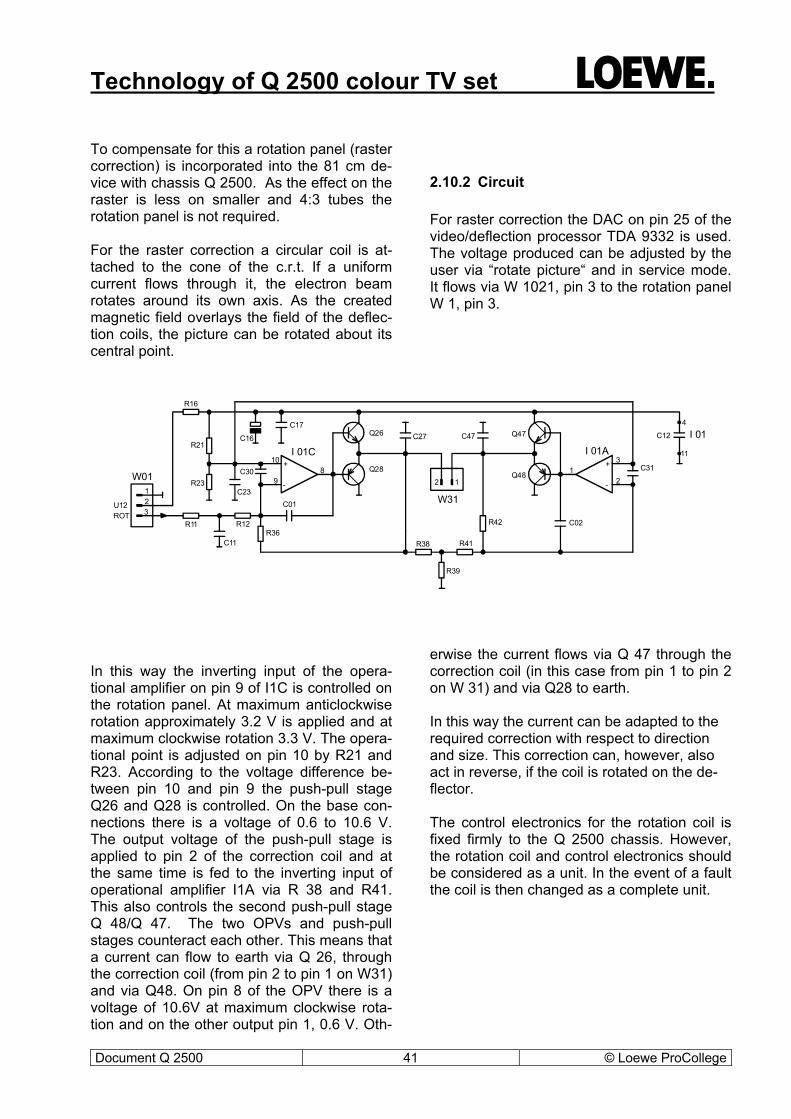
Technology of Q 2500 colour TV set
Document Q 2500 41 © Loewe ProCollege
To compensate for this a rotation panel (raster correction) is incorporated into the 81 cm de-vice with chassis Q 2500. As the effect on the raster is less on smaller and 4:3 tubes the rotation panel is not required. For the raster correction a circular coil is at-tached to the cone of the c.r.t. If a uniform current flows through it, the electron beam rotates around its own axis. As the created magnetic field overlays the field of the deflec-tion coils, the picture can be rotated about its central point.
2.10.2 Circuit For raster correction the DAC on pin 25 of the video/deflection processor TDA 9332 is used. The voltage produced can be adjusted by the user via “rotate picture“ and in service mode. It flows via W 1021, pin 3 to the rotation panel W 1, pin 3.
In this way the inverting input of the opera-tional amplifier on pin 9 of I1C is controlled on the rotation panel. At maximum anticlockwise rotation approximately 3.2 V is applied and at maximum clockwise rotation 3.3 V. The opera-tional point is adjusted on pin 10 by R21 and R23. According to the voltage difference be-tween pin 10 and pin 9 the push-pull stage Q26 and Q28 is controlled. On the base con-nections there is a voltage of 0.6 to 10.6 V. The output voltage of the push-pull stage is applied to pin 2 of the correction coil and at the same time is fed to the inverting input of operational amplifier I1A via R 38 and R41. This also controls the second push-pull stage Q 48/Q 47. The two OPVs and push-pull stages counteract each other. This means that a current can flow to earth via Q 26, through the correction coil (from pin 2 to pin 1 on W31) and via Q48. On pin 8 of the OPV there is a voltage of 10.6V at maximum clockwise rota-tion and on the other output pin 1, 0.6 V. Oth-
erwise the current flows via Q 47 through the correction coil (in this case from pin 1 to pin 2 on W 31) and via Q28 to earth. In this way the current can be adapted to the required correction with respect to direction and size. This correction can, however, also act in reverse, if the coil is rotated on the de-flector. The control electronics for the rotation coil is fixed firmly to the Q 2500 chassis. However, the rotation coil and control electronics should be considered as a unit. In the event of a fault the coil is then changed as a complete unit.
4
11
12
3
-
++
-
89
10
123
12
Q26
Q28
C16
R11 R12
R16
R21
R23
R36R38 R41
R42 C02
C17
C23
C27 C47
Q48
Q47
C01
R39
ROTU12
C12
C11
C30 C31
W31
I 01I 01AI 01C
W01

Technology of Q 2500 colour TV set
Document Q 2500 42 © Loewe ProCollege
2.11 NF output stages The two amplitude controlled VF signals are output from pins 56 and 57 of MSP 3411 on the signal board. The signals are applied to the base of transistors Q2081/2083. The tran-sistors are switched as impedance converters
to prevent, as far as possible, the coupling of interference pulses on the VF wires between MSP and the output ICs. The VF signals reach the two output stages via the coupling capacitors C 2082/476. In between are the two mute transistors Q 1586/88. (See signal board).
The output stages are implemented easily as all control processors (volume, tone, balance) as well as base width switching are processed in the MSP. Compared to previous models the Q 2500 has new output stages. TDA 7296 is equipped with an internal mute function that removes any residual on and off switching interference that is not fully suppressed by the additional mute switching.
The internal mute switching is controlled on pins 9/10. If the voltage on the pins is <3 V, then the output stages is muted. These two pins are controlled via R/C combinations via UMUTE. On start-up the two capacitors C 479/C 489 are charged slowly via the load resistors R 471/R 476 and R 477. The mute function in the IC is achieved via a voltage differential on pin 9 and pin 10. As long as pin 9 is more positive than pin 10, then the output of IC internal is muted. This is achieved on start-up/ shutdown by the R/C combination with various time constants.
R466
R468
R475
C475
R485
C485C488
L479
B214
B222
B210
W471
1
2
R489 C481
W481
1
2
R477
R471 R469
Q469
C48
9
W61013pol
1 2 3 4 5W470
9
1
2
3
4
5
6
7
8
W21113pol
1 2 3 4 5 6
I484TDA7296
15
14
1310
98
76 4
3
2
1
TDA7296I474
15
14
1310
98
76 4
3
2
1
R492
R488
R484
R483
R482
R479
R478
R476
R474
R473
R472
R467
L489
C492
C487 C486
C48
4
C483
C482C079
C47
8
C477C476
C474
C473C472C471
C468
C467
C466
D491
D474
U12
U+NF
U+NF
U+NF
U+NF
U+NFU+NF
U-NF
U-NF
U-NFU-NF
UM
UTE
RSI
G
LS-R
LS-L
Mut
e
Q2500 Stereo sound output stage
9
1
2
3
4
5
6
7
8
9 pin Cubeconnector
UM
UTE

Technology of Q 2500 colour TV set
Document Q 2500 43 © Loewe ProCollege
On start-up C 479/22 µF is very quickly charged up by R 471/22 k. For C 489/22 µF charging occurs more slowly via R 477/10 k and R 4476/33 k. This means that in the charging phase pin 9 is more positive with respect to pin 10. On shut down C 489 dis-charges rapidly via D 474 (which releases R 476) and R 477. Pin 9 is again more positive with respect to pin 10 and mute is imple-mented again internally. TDA 7296 can be considered to be an opera-tional amplifier. It is controlled by its non-inverting input pin 3. The amplification is cal-culated from the negative feedback combina-tion R 478/473. This results in R 478 22 k V = 1 + --------- = 1 + -------- = 33 R 473 0.68 k The amplified signal is felt on pin 14 and for the left channel is fed to the loudspeakers via L 479. The R 479/C 471 combination is necessary for an internal bootstrap. In addition, the output phase is equipped with an overload and tem-perature protection circuit. The two output stages are supplied with volt-age symmetrically. It is taken from the trans-former at zero potential and rectified and smoothed by D 686/687 and C 687. With the help of the R/C combination 466 and 468 it is split into +/- 18 V (see also power supply). This measure achieves a halving of the peak current by the rectifier diodes D 686/687 and a higher undistorted output performance, espe-cially for low frequencies. An output stage without any electrolytic ca-pacitors contributes to this.

Technology of Q 2500 colour TV set
Document Q 2500 44 © Loewe ProCollege
3 Receiver components
3.1 HF/IF unit Four receive components can be used in de-vices with Q 2500 chassis. One is the terres-trial tuner, or HF/IF component, which proc-esses frequencies from 47 MHz to 860 MHz. This hyperband tuner is located on the basic board. Second is the single SAT or dual SAT receiver for the first IF from 950 MHz to 2150 MHz. This is partly a standard feature or can be retrofitted for certain sets. In addition, for full IP sets a PIP-HF/IF unit for the reception of terrestrial signals is incorpo-rated into the hyperband range. In this case, however, the audio band is dispensed with, as picture for picture only video signals are re-quired. This is also built into the basic board. With this equipment the set is able to process all television signals, irrespective of whether they are received by terrestrial antennae or via cable units, and even when derived from parabolic antennae.
3.1.1 HF/IF components A HF/IF combination is also used. All func-tions for current European television stan-dards are located in one housing, with two provisos. The IF consists of only one picture IF. The audio demodulation takes place in the audio IC on the signal board. From the IF component only the sound IF is supplied as broadband. This means that the ceramic transducer and an expensive sound/IF switch are not re-quired. Secondly, for lower price models not destined for export HF-IF, designed only for PAL and SECAM BG, is used. In this case, the change-over to SECAM L and NTSC and the components necessary for this are not required. This means the two designs are hardware and software compatible. The following block circuit diagram shows the multi-standard design. Some of the compo-nents are not fitted to the BG version. As in earlier models, the electronics is housed in an HF proof folding housing.

Technology of Q 2500 colour TV set
Document Q 2500 45 © Loewe ProCollege
M,N
45 M
Hz
high
pas
s
27 M
Hz
trap
IF
TAG
CV
33
IF
A
nt in
Ant
out
po
wer
spl
itter
BS
C
V9
BS
LOP
4P
5V
5
V5A
FC
P
M
, N, B
G, I,
DK,
L, L
1 MN BL I L1 PN
B A
Ant
enne
n S
plitt
er M
AS
V9
SC
LS
DA
V9
1 2
M
L1
1 2M
N
L1
BL
CVB
S
AF
M
IF-AGC
SSIF
Syst.
: M
, N, B
G, I,
DK,
L, L
1
Tune
r
ZF
reje
ctio
n
Hig
h Ba
nd C
Low
Ban
d A
Mid
Ban
d C
on/o
ff
on/o
ff
on/off
Mix
er
Mix
er
Mix
er
osc
osc
osc
high
mid low
NO
R
PLL
0 1 2 3 7
IDC
70-150mV
ZF-in
34,4
40,4
32,3
833
,4
I,DK
,L
BG
,L10 2 1
M,N
BG
,I,D
K,L,
L1
d =
25 d
B
M o
. L1 SIF
5....
10m
V
Tune
r AG
C
SIF
AG
C
SIF
Am
pl.
VIF
Am
plifi
er
Tune
rAG
CVI
FAG
C AE
TOP
Cbl
Cv AGC
T PLL
L1
Tune
r A
FC
4,5
5,5
5,7
4
FPLL
VCO
TWD
Vide
o De
mod
ulat
orAm
plifi
er
AFC
Dete
ctor
TDA
9818
QSS
- In
ter-
carr
ier M
ixer
AM D
emod
.
FM-P
LL-
Dem
odul
ator
Volta
geR
ef.
CA
F
+5V
C SAG
CPNpo
s./n
eg.s
witc
h
Mix
er O
sc IC
CC
VS

Technology of Q 2500 colour TV set
Document Q 2500 46 © Loewe ProCollege
3.2 DVB Board
3.2.1 Overview The DVB decoder is able to convert DVB sig-nals that are transmitted free to air via satellite into the appropriate analogue audio and video signals, which are then fed to the signal proc-essing of the TV chassis.
For the conversion of the L band signal de-rived from LNC or a multiswitch, the combi-tuner of the satellite unit Sat 6 is designed as an assembly set or retrofit set for the Q 2500 chassis. It also supports the interface to an integrated online module.
The following block diagram shows the princi-pal architecture of the Sat 6 and DVB de-coder. The interface between Sat 6 and the DVB decoder is formed from quasi-analogue I and Q signals, the AGC signal, the IIC bus and a port used for DISEqC. The IQ signals are derived in the satellite tuner by quadrature mixing of the second IF (479.5 MHz) in the base band. The AGC signal provides ampli-tude control of the IQ outputs of the tuner. As the Sat 6 unit is able to process analogue and digital signals, both the DVB controller and the TV controller have access to the tuner and the LNC supply. The switching of the IIC buses used for this is achieved by the TV controller driven by the Sat 6 unit.
The processing of DVB signals from the tuner base band interface to the analogue output is achieved by two high integration chips. The first is the front-end component STV0299B (ST microelectronics) that digitises the IQ sig-nals coming from the tuner by means of dual ADCs, demodulates them (carrier and pulse extraction) and carries out Forward Error Cor-rection. The second component is the MPEG-2 demultiplexer-, decoder-, backend- and con-troller chip STi5500 (ST Microelectronics), which demultiplexes the MPEG-2 transport beam, feeds the selected audio and video components to the MPEG-2 decoder for de-compression, decodes them and then con-verts them into analogue output signals. The STi5500 also has an integrated 32-bit RISC
Sat 6
DVB-DecoderAnalogueAV progr.
Analogue/Digital-Sat.-Tuner
LNC-Control
CVBS
Sound-ZFor L-R
I-Signal
Q-Signal
AGC
I2C-BusDVB
I2C-BusTV
DISEqC
Satelliteantenna ADC
QPSK,FEC
I2C-Bus
Demux,DescramblerAV-DecoderV-EncoderController
27 MHzVCXO
2+2 MBSDRAM
Audio -DAC
2+2MBDRAM
1+1MBFlash
128 kBEAROM
RGB
S-Video to Scart-Matrix
Audio L-R toScart-Matrix
2x RS 232 toTV-Controller andOnline-Modul

Technology of Q 2500 colour TV set
Document Q 2500 47 © Loewe ProCollege
controller that forms the core of an independ-ent processor subsystem. It is responsible for the control and diagnosis of the other func-tional units of the DVB decoder module. Commands and data are exchanged via a serial interface to the TV controller. In addi-tion, the DVB is responsible for applications such as the Electronic Program Guide for DVB programmes. In this case the on screen display from the OSD component of the MPEG-2 video decoder is produced. For communication between the TV controller and the controller of the online modules, the data is transferred transparently between the two serial interfaces.

Technology of Q 2500 colour TV set
Document Q 2500 48 © Loewe ProCollege
3.3 Features and parameters 3.3.1 DVB internal features
Feature Standard/value range Notes
General
Receiving and decoding of DVB compatible free to air signals via satellite
Implementation as integrated module for incorporation or retrofitting in Q 2500
Q2500 basic, medium, high end
Operational control integrated into the Personal Control System
Electronic Programme Guide based on standard DVB-SI
Pre-programming ASTRA 19.2° East and Eutelsat 13° East
MPEG-2 main Profile@Main level 720x576 Pixel, 25 Hz
Support for 4:3 and 16:9 source format (letterbox filter-ing) and 4:3 display format (16:9 display format by scal-ing in TV up converter)
Pan&Scan is not used
Teletext processing to DVB teletext standard ETS 300 472, s. [5] Reinsertion in the Y sig-nal
Support for DVB radio programmes

Technology of Q 2500 colour TV set
Document Q 2500 49 © Loewe ProCollege
Feature Standard/ value range
Notes
Satellite front end
Demodulation and channel decoding to DVB satellite standard
Use of the combituners (analogue/digital) of the Sat-6 satellite unit
Input level area 45...80 dBµV to 75 Ohm
Input frequency level 950...2150 MHz
Input socket F female, 75 Ohm
IF wideband 36 MHz -3 dB
Demodulation QPSK
Demodulation QPSK
Symbol rate 15...30 Mbaud 1...30 Mbaud ad-justable 15...30 Mbaud guaranteed
Forward Error Correction Viterbi, De-interleaving and Reed Solomon
Use of the LNC voltage generation of the Sat 6 satellite unit or an optional switch fitted directly on the DVB mod-ule
Option for antenna control 13/18 V, 0/22 kHz, DiS-EqC Tone Burst, DiS-EqC 1.1(partial)
LNC current 400 mA

Technology of Q 2500 colour TV set
Document Q 2500 50 © Loewe ProCollege
Feature Standard/ value range
Notes
Audio/video backend
Interfaces to chassis FBAS/audio input (SAT6), RGB output, S video/FBAS output, au-dio output (Stereo)
Controller and graphics
Controller 32 bit RISC controller, 50 MHz clock
Working memory 4 Mbyte DRAM, 2 Mbyte Flash ROM
MPEG and video memory 4 Mbyte SDRAM
Graphics Internal OSD with 720x576 pixel resolu-tion; to 8 bit/pixel, 4 bit/pixel used
OSD comparison in service mode (background bright-ness)
Y_nominal+/-6 levels

Technology of Q 2500 colour TV set
Document Q 2500 51 © Loewe ProCollege
Feature Standard/value range Notes
Software
Local update of operating software DVB module: via service socket (RS232-Interface, 5 V)
Generation and update of programme list via various options: pre-programming, frequency search procedure, semi-automatic programme search (manual setting of carrier currents and automatic search for carrier current levels)
Separate search procedure for DVB television and radio programmes
Automatic setup of audio channels (default: configuration in menu language) and display of options (menu tree: sound/voice)
Programme information: Decoding and display of Pre-sent_Event and Following_Event via DVB-SI and Teletext
Generation of an SI database for freely selectable pre-ferred programmes
With Next-View harmonised Loewe Digital EPG
Separate Radio EPG
Detection of encrypted programmes
Detection of inconsistent data, robust reaction and gen-eration of messages on fault detection
DVB Service Mode for comparison (VCXO), diagnostics (Test picture) and deletion of DVB-EAROMs

Technology of Q 2500 colour TV set
Document Q 2500 52 © Loewe ProCollege
3.3.2 DVB/TV features
Feature Standard/Value range Notes
PIP: DVB in TV or VGA, TV in DVB Satellite: 2 in-dependent leads and Sat 6 twin fitting nec-essary!
Automatic picture format switching
Creation of a common programme list with analogue and digital programmes with special recognition of the digital programmes
„D“
Separate radio mode with radio programme list
3.3.3 Architecture The following block diagram shows the archi-tecture of the DVB decoder for Q 2500.

Technology of Q 2500 colour TV set
Document Q 2500 53 © Loewe ProCollege
16 M
Bit
FLA
SH
32 M
Bit
FPM
-DR
AM
CO
NTR
OLL
ERD
EMU
XVI
DEO
DEC
OD
ERA
UD
IODE
CO
DER
VIDE
OEN
CO
DER
32
MB
it S
DR
AM
Audi
o-D
AC
QPS
K-
Dem
od.
FEC
CVB
S/Y
Audi
o L/
R
RG
B/Y
C-
driv
er
Pow
er S
uppl
y
27M
Hz
VCXO
STI5
500
2 *
TE28
F008
B3T9
0KM
416V
1200
CT-
6
KM41
6S10
20C
T-G
8
MK
2727
S 1MBi
tEA
RO
MAT
29LV
010-
25TC
STV0
299
CS4
334
Qua
rz4M
Hz
Qua
rz13
.5M
Hz
SER
.3
SER
.1
CO
NTR
OL
27M
Hz
&PO
N-
RES
ET
Deb
ug/J
PI
EMI-B
US
SD-B
US
RES
I2C
SER
.TR
ANSP
.
RG
B/Y/
C
to S
igna
lboa
rdto
/from
SAT
6 un
itto
/from
Sig
nalb
oard
to/fr
om T
VO
3.3V
I/QI2
CAG
C
3.3V
supp
ly
from
Bas
ic-B
oard
TV-C
ontr.
/Ser
v.so
cket
s
CV
BS
-A
udio
Sw
itch
to S
igna
lboa
rdfro
m S
AT6-
Ein
heit
RG
B
Y-D
VBL/
R-D
VB
L/R
-Ana
CVB
S-A
na
C-D
VB
DVB
-AN
A
U14
U25
+5V
cont
rolle
r
U5
+12V
cont
rolle
r+5
Vco
ntro
ller
U12
U5A
Dig
.Aud
io
DVB
-Dec
oder
Q25
00
W71
00W
7120
W77
81W
7943
W75
06W
7680
W76
11
W79
16

Technology of Q 2500 colour TV set
Document Q 2500 54 © Loewe ProCollege
3.4 Components
3.4.1 Satellite front end
3.4.2 Functional distribution The satellite front-end processes the signal of the 1. satellite IF coming from the Universal-LNC or Multiswitch up to the MPEG-2 carrier current, fed to the MPEG-2 demulti-plexer/decoder. It also houses the compo-nents for the supply and control of the an-tenna units. The functions mentioned are dis-tributed to blocks of the Sat 6 (Tuner, LNC supply) unit DVB decoder (AD conversion, demodulation, forward error correction). The separation is implemented via an ana-logue/digital satellite tuner in order to be able to use redundancy free processing of TV and DVB signals. The reasons for the choice of interfaces are:
Fewer requirements for the screening of the Sat 6 unit and low-interference quasi-analogue baseband interface to DVB decoder. Due to the functional unity, the relevant pa-rameters for DVB reception of the Sat 6 unit are specified in the following.
3.4.3 Tuner
The tuner converts the signal of the 1. satellite IF in the base band. Signal processing for analogue and DVB signals is distinguished only in respect of demodulation, and is there-fore almost identical with respect to the pre-filtering and amplification stages, mixing on the 2. IF, channel selection and amplification. For this the implementation of an ana-logue/digital combi-tuner is advised. The Sat 6 unit incorporates the BS2W7VG2002 (Sharp) analogue/digital sat-ellite tuner

Technology of Q 2500 colour TV set
Document Q 2500 55 © Loewe ProCollege
(TSA5523)
Philipstuner
5V30V
AS
CVBS
Ulnc
SGS LNB2
LM2574SAA1300
SDA
4
U26
SCL SDA Ud U5
DiS
EqC
SCL4
TDA6151-5x
P4 P5 P7 P0 P1
+/-/BBAmplitude
FBAS
SIF
P2: M
ute
P3: C
lam
ping
on/
off
Mute
CVBS
SIF
W760 toSignal-Board
W770 fromBasic-Board
Sat6: Main - analog/digital Twin: analog
SCL
SDA
LNB1/2
SGS LNB2
LM2574SAA1300
Tun
B6
STV0056
FM In
BB In
SCL
SDA
U5
U12
Video-TP
CVBSB5
I/Odigi
tal
anal
og
Max4546
AFT1
AFT2 TSA5523P6
SCL4 SDA4 U5 U12
5.5 10
f/MHz
f/MHz
10
Iout
QoutRF in
B2 B4
U16
U26
GN
D
W390 toBasic-Board
5V 30V
DiS
EqC12V
SCL4
SCD
4
N.C
.
GN
D
W260 toBasic-Board
AG
CSC
L D
VB
SDA
DV
BD
iSEq
CG
ND
W120 toDVB-Board
AG
C In
SCL
Sat
SDA
Sat
AF L
AF R
FBAS
W680 toSignal-Board
S1 Vid Out
S1 L Out
S1 R Out
Iout DVB
Qout DVB
W100 toDVB-Board
Port
P0 ..
. P7
S2 V
id R
trnS3
Vid
Rtrn
S2 V
id O
ut

Technology of Q 2500 colour TV set
Document Q 2500 56 © Loewe ProCollege
3.4.4 DVB demodulation and fault correc-tion
Additional signal processing comprises: - AD conversion of the quadrature sig-
nals from the tuner, - QPSK demodulation and
channel decoding in the form of For-ward Error Correction.
Demodulation and channel decoding are compatible with ETS 300 421. In practice an in-house chip solution is used for all three functions. For reasons of interface compatibil-ity with the MPEG decoder, the STV0299B module from ST Microelectronics is used. There then follows specification of the practi-cal implementation, as well as parameters, which in ETS 300421 are only partially set.

Technology of Q 2500 colour TV set
Document Q 2500 57 © Loewe ProCollege
Parameter Value/algorithm Notes
Chip STV0299B Manufacturer: ST Microelec-tronics
ADC
ADC-Type Dual Resolution 2*6 bit Sampling Clock Variable, dependent on symbol
rate Generated by on chip PLL
IQ input voltage 1 Vss
Demodulation
Procedure Coherent grey coded QPSK demodulation
Symbol rate range STV0299B 1...45 Mbaud Symbol rate over all (including tuner) without neighbouring channel assignment
1...30 Mbaud Lower limit: Phase noise of tuner Upper limit: IF bandwidth of tuner
Symbol rate over all with neighbouring channel assign-ment
15...30 Mbaud
Preferred value for symbol rate 27.5 and 22 Mbaud Used in frequency search pro-cedure
Other symbol rates Decoding from NIT (delivery system descriptor) of Barker Channel or manual selection
Roll off filtering Half Nyquist Roll off factor 0.20 (20 %); 0.35 (0.35 %) Used roll off factor 0.35 (35 %) Carrier recovery Digital PLL with internal de-
rotator and hardware lock-in detector
Pulse recovery Internal digital PLL Processing of the normal or inverting spectrum

Technology of Q 2500 colour TV set
Document Q 2500 58 © Loewe ProCollege
Parameter Value/algorithm Notes
Chip STV0299B Manufacturer: ST Microelec-tronics
AGC AGC analogue/digital tuner with PWM output. Internal digital AGC on power optimisation within the signal bandwidth.
AFC digital software AFC
Forward Error Correction (FEC)
1. FEC stage Viterbi decoder - Constraint length 7 - Rate ½ - Other code rates ½, 2/3, ¾, 5/6, 7/8 - Rate selection Automatic or manual 2. De-interleaver - Synchronous word extraction - Convolutional interleaver - Depth 12 3. Reed Solomon Decoder - Number of parity bytes 12 - Block length 204 - Correctable byte error 8 - Energy dispersal de-scrambler
Other
- Carrier current output Parallel or serial - Used mode for output Serial - Control IIC bus - On Chip Error Monitoring
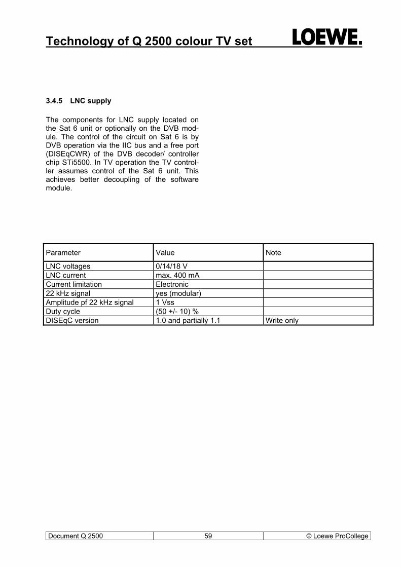
Technology of Q 2500 colour TV set
Document Q 2500 59 © Loewe ProCollege
3.4.5 LNC supply The components for LNC supply located on the Sat 6 unit or optionally on the DVB mod-ule. The control of the circuit on Sat 6 is by DVB operation via the IIC bus and a free port (DISEqCWR) of the DVB decoder/ controller chip STi5500. In TV operation the TV control-ler assumes control of the Sat 6 unit. This achieves better decoupling of the software module.
Parameter Value Note
LNC voltages 0/14/18 V LNC current max. 400 mA Current limitation Electronic 22 kHz signal yes (modular) Amplitude pf 22 kHz signal 1 Vss Duty cycle (50 +/- 10) % DISEqC version 1.0 and partially 1.1 Write only

Technology of Q 2500 colour TV set
Document Q 2500 60 © Loewe ProCollege
4 Signal board Mounted on the signal board, which is linked to the basic board via connectors, are all the necessary building blocks for device control, interface switching, video, audio and videotext processing. These are: - The device control with computer circuit,
operating software and the EAROM for the storing of system data and customer spe-cific calibration values.
- Production of system cycle frequency nec-
essary for a digital design. - The digital IC’s necessary for picture signal
processing. - The video/deflection processor for the pro-
duction and synchronization of control pulses.
- Digital audio processing for analogue trans-
ferred information and NICAM decoding. - The teletext decoder, integrated into the
SDA 6000, with page memory, in which up to 3000 text pages, according to design, can be saved and which also generates the OSD for the user control.
- The signal and interface selection by corre-
sponding IC’s controllable via the I²C bus. - Optional IC’s for video processing, picture
in picture.
4.1 Device control Full device control is implemented by a Sie-mens 16 bit processor (SDA 6000) together with Loewe operating software. The teletext function is also integrated into the SDA 6000. A standalone teletext processor is therefore not necessary. All processes in the digital signal preparation, in the tuners and interface selection are checked and controlled via a microcomputer integrated into the SDA 6000. The processor is also known as the CCU (Central Control Unit). It also supports the operating, tuning and storage system on the frequency synthesis principle. Without the DVB module there are 220 programme storage locations, and with the DVB board there are 1470. The pro-gramme locations are available for TV and also for radio operation. The total number of stored programs must not exceed 220 (1470). For the AV inputs six additional places are reserved. Operating software is held in an external EPROM. For the storage of c.r.t. and system specific data there is an EAROM for device control. The latter also contains programme location information. All three modules, CCU, EPROM and EAROM are mounted on the signal board. The remote maintenance sensor permits con-trol of possible device functions. The chassis tuning is also carried out by remote mainte-nance. For this, the sensor IC generates a serial data word for each command that is transferred to the receiver with a delay. This signal is de-modulated by the IR receiver and prepared in such a way that it can be sent directly to the CCU as an RSIG signal. The CCU detects the local operating com-mands on a line by the different voltage levels.

Technology of Q 2500 colour TV set
Dokument Q 2500 61 © Loewe ProCollege
The CCU operates as a central control and information module. The software is held in as external EPROM. It concerns data necessary for the control of the digital IC’s, tuning, OSD’s etc. For control of all processes in the device the C 161 bus system: - generates I²C bus 0 transmits data to and from the EAROM. In
addition it controls the picture and audio signal processing.
- generates I²C bus1 controls the 1st and 2nd receiver unit on
the basic board, the switching IC’s for the audio and video signals on the signal board and the optional PIP processor.
- generates I²C bus 2 controls the satellite units and partially con-
trols the switching IC´s for audio and video.
Switchinginputs and outputs
to DVB/TV-Online
6 MHz
IR trans- mitter
Standby and ON - LED
SDA 6000
Reset out
Reset in
Standby PSU
Localoperation
IRreciever
SAT or Twin-SAT
Audio processingRS232 Service/Control
IR-Out Euro/AV
TVO
Video processing50 Hz 100Hz
EPROM I 2926
EAROM 1
EAROM 2
SDRAM
Deflection
Block diagram - Device control
Interface ICs
PIPprocessor
PIPreciever unit
Receiver unit 1
I2C-Bus 1
I2C-Bus 0
I2C-Bus 2
Addresses
Data

Technology of Q 2500 colour TV set
Document Q 2500 62 © Loewe ProCollege
4.1.1 The infrared sensor With the state-of-the-art IR transmitter all de-vice functions, with a few exceptions, can be controlled remotely. Starting with on/off via control functions such as volume/contrast, to control of the satellite antenna.
To ensure remote control of all functions, but-tons must have double or extended switching functionality. Operation is via a well-organised menu struc-ture. For this a cursor cross is provided on the remote control. In addition, frequently used functions can be assigned to the four colour keys. This does not set the command in the remote control, but a corresponding value in the device software. In the high-quality system
A B C D E F G
1
2
3
4
5
6
7
A B C D E F G
1
2
3
4
5
6
7
UB
UB
UB
UB
UB
123
54
14X101Y 2
00Y 3TO 4
RES5T1
6Vdd7XT28XT1904Y 10
05Y1116X 1217X13
06Y14
07Y15
13X16
12X17
11X18
10X19
Vss20
Lou21
03Y22
02Y23
15X24
1
2
1
2 1
2
1
2
1
2
1
2 1
2
1
2
1
2 1
2
1
2
1
2 1
2
1
2
1
2 1
2
1
2
1
2
1
2
1
2 1
2
1
2
1
2
1
2 1
2
1
2
1
2
1
2
1
2 1
2
1
2
Z1 Z4
Z17
Z30
Z27
Z24
Z21Z20
Z16
Z14Z13
Z11Z10
Z5
Z2 Z3
Z6
Z12
Z15
Z18
Z19 Z22
Z23
Z25 Z26
Z28 Z31
D121
X111C112
R124
R122
Q121
D105
Z29
Z8Z7
Z9
C111
SYM
POL-
LCD
2x1,5V
FB Control 150
FB Control 10
R101
R118D118
D117
R112
R113
R416
R414
R407
Q404
R404
Q414
R411
C423
R408 R403 R402 R406
R111
R120 R121
Q416
R410
R106C101
V=
1 2 3
4 5 6
7 8 9
0
T M E i
OK
rt gn ge bl
D11
4
I 101
R117

Technology of Q 2500 colour TV set
Document Q 2500 63 © Loewe ProCollege
range device the various functions are sup-ported by an LCD display. An 84 C 122 Philips microprocessor is used in the remote control for the Q 2500 chassis (Control 10 for Loewe Systems and Control 150 for Loewe.). This is an 8 bit standalone microcontroller, especially designed for use in infrared remote controls. It has very little ex-ternal wiring and is able to control the trans-mitter diode directly via an amplifying transis-
tor. The modulator is incorporated into the IC. The processor is equipped with Loewe spe-cific software, which is mask programmed. To operate the Q 2500 chassis, commands are issued as RC 5 code, level 0. The operating commands are formed on the transmitter keyboard by linking a Y input (Y4 Y7) with an X input (X10 X17).
Internal circuit 84C122
2 13 23 2422 10 11 14 15 19 18 17 13 416 12
Batterycheck
RSIG
TO/INT
21
8
97
20
6
5
UB
T1
VSS
WDT
fosz / 30
Output Driver
Y00Y01
Y02Y03
Y04Y05
Y06Y07
X10X11
X12X13
X14X15
X16X17
ROM1k x 8
ROM32 byte
I 101 PCA84C122A T
X1114,3MHzOscillator
HardwareModulator
TO/INT

Technology of Q 2500 colour TV set
Document Q 2500 64 © Loewe ProCollege
The operating commands for videotext are specified as a sub-program in "Level 0". The transmitter IC produces a code word for each command and adds two start bits and a control bit. The two start bits are always H, and the control bit changes each time the but-ton is pressed. It indicates to the central con-trol unit, whether a new command is present, or the current command is still valid. This 14 bit codeword is modulated with a 36 kHz carrier and applied serially to pin 21 of 84 C 122.
The digital Information is expressed by the step direction within the bit (Biphase). If the button is pressed for a long time on the report control the codeword is repeated after 114 ms. This signal is supplied to T 121 via resistor R 124, amplified and radiated via infrared di-ode D 121. The transmitter diode is now no longer covered by a dispersion window. This means the current can be reduced to f 900 mAss. The current can be taken directly from the battery, which means that no additional Elkos are necessary on the operating voltage.
On pins 8 and 9 of 84 C 122, the ceramic os-cillator X 111 is the component that deter-mines the frequency of the pulse oscillator for the synchronisation of the system and for the production of the carrier frequency (fTr = 1/12 fCycle). Using the ceramic oscillator X 111 means that tuning of the cycle frequency is not needed.
The circuit is functional at an operating volt-age of 2.5 – 3.5 V and draws a normally ener-gised circuit current of = 1 uA and an operat-ing current of 35 mA. The transmitter thereby achieves a range of >10 m. The voltage source is two micro-alkali-manganese batteries.
1,78 1,781,78
L L L L L L H H H H H H
Adress bitsStart bits Command bits
t (ms)1,78 1,78 1,78 1,78 1,78 1,78
Carrier = 36kHzExample:Codeword for command search
14 BIT - Codeword
14 BIT = 24,92 ms
L H

Technology of Q 2500 colour TV set
Document Q 2500 65 © Loewe ProCollege
After switching to the service mode, chassis tuning is implemented with the FB transmitter. The service mode is called up by pressing the functional button “?“ four times, so that the “Service“ display appears, and then pressing the “M“ button on the remote control within one second. Then using the curser buttons, the individual tuning functions can be called up. Tuning is also carried out using the cursor keys. The data is initially stored in the working memory C 161 and is only transferred to the memory on operation of the "ok" memory but-ton. Once returned to normal FS operation, use the "E" button to return to remote opera-tion. Pressing the Z 1 button switches the remote control processor to another mode. This means that the transmitter can be used for both a videorecorder and DVD player from Loewe. For the videorecorder, however, con-trol is only possible with Korythso code, as used by Panasonic. For the DVD player we use the RC 6 code. If the remote control is not used in the video-recorder or DVD mode for 20 sec, then it automatically switches back to the TV mode. The video or DVD mode is displayed for Con-trol 10 by the LCD and for Control 150 by an LED on pin 2 (Y1) and pin 3 (Y0). For Control 10 the LCD is controlled from ports Y3 to Y7. Up to Y3 these are also used to query the button matrix. The operating voltage is also monitored in Control 10 and displayed correspondingly in the LCD. Measurement of the battery voltage is carried out by transistors Q 416, Q 414 and Q 404 on pin 5 of 84 C 122.
4.1.2 Infrared receiver
The IR receiver on the local control unit is a thick film circuit and is fully encapsulated. The IR signal from the transmitter is converted into an electrical signal by the receiving diode, amplified and prepared in such a way that it is available on the output as 2 Vss. With the next transistor Q 8202 on the local control unit the signal is amplified to 5 Vss. In this way the IR decoder in SDA 6000 can be safely controlled via pin 5 Via IC I 2716 and transistors Q 2721, Q 2731 and Q 2741 the IR signal is applied to pin 8 on each of the three Euro sockets. This allows hidden videorecorders to be remotely con-trolled via the IR receiver of the television set and the AV switching voltage line (see AV operation). Via Q 2823 the signal reaches transistor Q 2862 on pin connector W 1076. Via W 1076 the IR signal is supplied to a connected online-box. The pulse width for the RC 5 code of the re-mote control is about. 900 µs. If a connected Multi Media Component is operated with the Control@media IR keyboard, the data is not transferred with the slow RC 5 code, but with an RC MM code (MM-Multi Media) designed for fast data transfer. The pulse width for the RC MM code is 167 µs. The pulse width of 167 µs requires an IR-receiver with a very short time constant. Therefore, in Multi Media devices a special IR receiver is used, which for operational pur-
Q8202
R8217
R8216C8216U5SB
R8205I 8216 Infraredreciever
RC5
5V0V

Technology of Q 2500 colour TV set
Document Q 2500 66 © Loewe ProCollege
poses cannot be replaced by one from a nor-mal TV set.
4.1.3 The SDA 6000 central control unit
A Siemens SDA 6000 is used in the Q 2500 chassis for control of device functions. This 16 bit processor is a development of the C 166 family of single chip CMOS microcontrollers. It combines excellent CPU characteristics of up to 8 million computation operations per sec-ond with high functionality, flexibility and high capacity input and output ports. The SAD 6000 has 5 Ports (Port 2 – Port 6) with a total of 44 inputs and outputs. It was designed es-pecially for applications, where cost plays a critical role. This makes the processor suitable for use in colour TV sets.
In the Q 2500 chassis the processor must fulfil the following functions: - Oscillator for generation of the CPU cycle
frequency. - Generation of the clock frequency for the
bus systems.
- Processing of the RSIG signals and local operation commands.
- Generation of the I²C bus systems for con-
trol of the HF/IF units, processing of pic-tures, video text, PIP and audio, for com-munication with the memory IC, the SAT receiver unit and the interface selection.
16...21
16
16
16
32
16
16
16
16
4
7881563
CVBS1
CVBS1Slicer1
Slicer2ACQ
AMI
ExternalBus
Interface
D-Cache
BootRom
I-CacheInstr./Data
X-Bus Instr./Data
PECInterrupt Controller
36 nodes (8 ext.)
CPU-CoreC166
Data
Data
Data
InternalRAM
2 Kbyte
OSC(6 MHz) XTAL
OCDS
JTAG
WatchdogRTCI2C-Bus
GPT2GPT1
T2
T3
T4
T5
T6
SPISSC
USARTASC
4-Channel
ADC7-bit
D-Synch
H V
Port 5 Port 3 Port 2 Port 4 Port 63 x 6 Bit
DAC
FIFO
GA SRU
XRAM2 KByte
SDA 6000

Technology of Q 2500 colour TV set
Document Q 2500 67 © Loewe ProCollege
- Control of LED’s for operating and standby display.
- Creation of further switching processes,
e.g. ON/OFF, AV transfer, etc. - Simulation of a clock synchronised by VPS-
information. - Timer function for programmable discon-
nect time and recording timer. - Code converter for IR commands for the
remote control of a video recorder via the AV voltage switching line and the Dolby surround unit.
- RS 232 for communication with the online
as well as the DVB module. - Digital Link Plus Control for the 3
Euro/AV sockets In order to fulfil the required tasks the follow-ing circuit components are combined in one chip: - C 16 core with CPU and interrupt controller - 2 kByte XRAM as working memory - Interface for the external ROM - Quarz controlled clock generator - Interface for the three I2C buses - Multifunctional timer - IR decoder - ON/OFF Flip-Flop - Reset circuit for internal reset - Reset circuit for external IC’s. - Ports P2 to P6 with 44 input and output
pins. Many of these functions are implemented not by the hardware of the processor, but by the Loewe-specific software.
4.1.4 Reset For correct functioning of the device, various reset pulses are necessary. The first required is a reset on pin 73 for the SDA 6000, as soon as its operating voltage U3.3 is available and the 6 MHz system cycle has run. This reset is produced by I 2941. After this reset the SDA 6000 starts to operate and implements and emits control commands. The microprocessor also has a reset on pin 8, produced by I 2946, if the circuit power supply has run and all IC’s have an operating volt-age. This reset is retarded in SDA 6000 and then emitted from pin 100 to the digital IC’s. RESET digital component input pin 8 The reset for this input is formed by a steep positive flank. As U3,3 is the last voltage switched by the power supply unit, this reset is coupled to the voltage. The reset pulse is cre-ated in I 2946 and is present on pin 8 of the microprocessor, if all IC’s in the chassis have an operating voltage. SDA 6000 can then be-gin controlling the IC’s. In addition the proces-sor also reacts, if the reset is not present on pin 8 or during operation. Normally 5 V is al-ways felt on a reset input, provided the device is fully switched on. RESET digital component output pin 100 Via this pin the microprocessor sends the re-set to the other circuits. This is coupled to in-put pin 8. In this way the processor can moni-tor the reset, and for transient voltage failures can prevent, the level on the reset line col-lapsing. On the other hand, the circuit also makes it possible for the SDA 6000 to emit a software controlled reset on pin 50 during op-eration In standby and on start up L level is initially felt on pin 100. Not until the SDA 6000 switches pin 100 to H level, does the L/H flank produce the reset for the IC’s. During opera-tion the reset inputs must be held permanently at H level, otherwise the working register will be deleted.

Technology of Q 2500 colour TV set
Document Q 2500 68 © Loewe ProCollege
This reset reaches MSP 3410 /pin 21, and the two VCP 3230/33 /pin 15. All other IC’s either do not need a reset or generate it on switching on the operating volt-age.
4.1.5 Creation of cycle frequency The internal oscillator of SDA 6000 is syn-chronised with a 6 MHz quarz on pins 108 and 109. The cycle frequency for the bus systems is obtained from this frequency by internal distribution. They are from 70 to 400 kHz re-spectively for the I²C bus systems. The cycle frequency is transferred under software con-trol depending on the current function.
4.1.6 Operational commands The SDA 6000 receives operational com-mands as serial data information by RSIG signal on pin 9. The local operating com-mands are applied to the CCU on pin 126 as various voltage values. Pin 126 operates as an ADC with 6 bit resolu-tion. By various voltage dividers on the three operating unit buttons, various voltage levels are produced. The voltage levels are digitised by the ADC, and based on the measured values the CCU issues the appropriate commands. The following voltages are produced by ma-nipulation of the various buttons: • • “+“ button - 0.5 V • “-“ button - 1.1 V • “ “ button - 1.8V The overtravel contact is connected to pin 93 of the CCU.
4.1.7 LED display The red standby LED is controlled via pin 96 of the CCU. In operation the remote control commands in RC5 code are acknowledged by transient illumination of the LED. For standby operation the pin is set to the H level and transistor Q 2853 thereby conducts, where-upon the LED illuminates. The ON LED is controlled via pin 78 with the ON/OFF-command. When the power supply is switched on this line is set to the L level, whereby the green ON LED also illuminates. SAT standby operation is indicated by illumination of the two LED’s.
4.1.8 ON/OFF function If a switch-on command is present, the output ON/OFF, pin 78 of the CCU is set to L level. This blocks transistor Q 8111 in the standby power supply, whereupon Q 8114 conducts and attracts the relay. The system voltage is able to reach the main power supply, which begins to operate. The device starts operating at the selected program location. The output is once again set to H level by an off command. With an ON/OFF command the two transistors Q 2961 and Q 2966, which form part of the mute circuit, are switched, thus suppressing input and output noises.
4.1.9 Protective circuit In order to avoid excessive high voltage, c.r.t. defects or other serious damage due to faults in the vertical deflection, caused by excessive beam current, the device is switched to standby. In addition, pin 94 of the CCU is set to H level. In normal operation L level is pre-sent (see description basic board Section 5.2 – 6.2).
Technology of Q 2500 colour TV set
Document Q 2500 69 © Loewe ProCollege
If an error occurs – H level on pin 94 of the CCU - the CCU swtiches the device after 2 seconds to standby operation.
4.1.10 AV operation The circuit is designed so that AV operation with switching voltage on programme loca-tions can be programmed. Setting is implemented in the menu under connect AV device. The menu makes clear the exact procedure for setting up or you can refer to the overview in the operating instructions. Monitoring of the switching voltage on pin 8 of the AV socket is implemented via transistors Q 2737/Q 2726 and Q 2746 for AV1/AV2 and AV3. The three emitter followers are connected respectively via voltage dividers to pins 125/124 and 127 of the CCU. In accordance with the Euro/AV standard, pin 8 of the AV socket is defined as 6V (16:9 op-eration) and 12 V (4:3 operation) AV opera-tion. The CCU monitors these voltages on its AV pins. By division of the respective voltages 6V = 1.3V and 12V = 2.6V on the pins of the CCU. If a switching voltage is detected by the CCU, this switches over to AV operation on corresponding menu selection. • IR signals For the remote operation of VTR devices via the TV-IR receiver the RSIG signal is applied to the Euro sockets pin 8. For this two signal paths are provided. In nor-mal and standby operation SDA 6000 pin 9 at H level switches transistor Q 2823, and pin 97, which is also on the signal path, is made high-resistant from SDA 6000, to avoid inter-ference. Via Q 2823 and I 2716 the RSIG sig-nal is passed on to the transistors for socket selection. Use of the recorder remote control is necessary for this.
There may be applications, however, for which the video recorder remote control is not available and the TV remote control emits another code that the recorder does not un-derstand. For this a video menu is provided in chassis Q 2500, which is called up in the re-mote control with “V=“. This allows the basic functions of the recorder to be used. If for “Connect video devices“ three devices are selected, they can all be controlled independ-ently of each other. In this operating mode the RSIG signal pre-sent on pin 5 of the CCU is controlled inter-nally via a code converter and then output via pin 97 of SDA 6000, which is now low resis-tant. The other signal path is identical with the first possibility. The code converter changes the RC 5 data words of level 0, as they are delivered to the IR receiver, to those of level 5, with which the video recorder operates. Secondly, the code converter changes the RC 5 command into the corresponding data word of the NEC code. Thirdly, the RC 5 commands are converted into the Korythso code. The three data words, both RC 5 of level 5, as well as the NEC code word and the Korythso code word, are emitted serially by SDA 6000 pin 97. This means that remote control of re-corders that operate with RC 5, NEC or Korythso code is possible. Of course, a recorder must be used that can process the remote control signal coming from the AV switching voltage line. For this most Loewe recorders have a converter. During output of the converted IR commands transistor Q 2823 is blocked with L level on pin 9 of the CCU. This prevents these signals being affected by IR signals from the receiver on the operating component. In order to achieve separate operation of the three devices connected to the two Euro sockets, the circuit also contains RSIG signal switching controlled by the CCU.

Technology of Q 2500 colour TV set
Document Q 2500 70 © Loewe ProCollege
This switching is implemented by multiplexer I 2716. The IC is controlled by the CCU via the outputs pin 15/80. According to the status, see table, the IRIN/IROUT signal is switched to the respective Euro/AV socket.
An optional online module can be controlled by transistor Q 2862.
The software for the RSIG signal switching is fitted with a load memory function. If there is no information about which socket should be used RSIG is applied to AV 1. If another socket is selected, the signal is then applied to this socket. If no socket is selected, the signal is applied to the one last used. This is true also for standby.
4.1.11 SAT standby In order to create a situation where a video machine can also receive signals from the SAT receiving unit, which is integrated into the unit, without the TV set needing to be in op-eration, the horizontal output stage in this op-erating mode is switched off. This is achieved by an H level emitted via pin 79 of the CCU. This switches transistor Q 2951 and the hori-zontal control pulse from the video/deflection processor TDA 9332 is lead to earth.
U5
U5SB
Q2823
Q2721
Q2856
R2826
R2859
Q2862
Q2741
D2856IR OUT
AB
IR S
IR IN IR receiver
Infrared signal path
5
9
97
805
9
312
10
13
15
U5
AV3 / Pin 8
AV2 / Pin 8
Q2731
AV1 / Pin 8
R2856
R27
17
Logik and code
converter
I 2801 SDA 6000 I 2716
Control
A B Output L L AV3 / Pin 8 H L AV1 / Pin 8 L H AV2 / Pin 8
RC out/TVOW 1076/2
IR outW1610/4
U5Q2902
R2903
IR-outW 1913/2

Technology of Q 2500 colour TV set
Document Q 2500 71 © Loewe ProCollege
As both the vertical and the RGB output stage obtain their operating voltage from the diode split transformer, this allows the entire c.r.t. to be switched off and the power input in this mode to be reduced. In normal operation pin 79 of the CCU is at L level and transistor Q 2951 is high resistance. The c.r.t. is switched off when: a) a timed recording for a video recorder is
being processed in the TV set. b) on switch off using the remote control, if
previously, via the video menu, a recorder has been set to record.
c) on switch off using the remote control, if
previously overplaying between the sock-ets of the TV has been activated.
d) Radio – operation is activated (after 20
sec.). In all these cases all other stages of the chas-sis are fully operational. Except for d) the sound in the MSP 3410 is switched off via the I²C bus.
4.1.12 SAT unit control Control of the Sat/TwinSat unit is implemented by the CCU via the I²C-Bus 2.
The SAT unit VI used is also able to control appropriately equipped switch boxes or LNCs via DiSEqC Level 1 (Digital Satellite Equip-ment Control). In this system pulse modulation of the 22 kHz signals allows data to be ex-changed between receiver and peripheral de-vices. This means that the current different LNC supply voltage switching information, 22 kHz and control function will be replaced and simplified by separate control lines.
In the standard, a logical 1 is defined as 11 periods of 22 kHz signals (0.5 ms) followed by a 1 ms pause (22 periods). The logical 0 is represented in reverse, i.e. 22 oscillations (1 ms) and then a 0.5 ms pause (11 oscillations). For this, each bit requires 1.5 ms for the trans-fer, which corresponds to a maximum transfer speed of 666 bits per second. After each
transferred telegram, there must be a pause of at least 6 ms (132 periods). Control is implemented according to the Sin-gle Master - Single/Multi Slave principle. Mas-ter is always the SAT receiver, and the exter-nal components (LNC multiswitch, etc.) are the slaves. Therefore, each communication from the receiver is started and the external components can only transfer data, after they have been requested to do so by the master. A command from the master contains a 1 byte frame, a 1 byte address, a 1 byte command and 1 or more bytes of data. The responses consist of a 1 byte frame and 1 or more bytes of data. Each byte is always followed by a parity bit (P) for error checking. The frame byte determines, whether the data is sent by the master or the slave. The ad-dress byte contains the information that de-termines which peripheral module (switchbox, LNC ....) is addressed. The command byte determines which switching function is to be implemented (selection LNC, level switching ....). In the data byte additional information can be exchanged. There is still enough free space in the DiSEqC command set for future requirements. This means that the system has built in futurability. For the DiSEqC control the SDA 6000 has an input and output respectively. Communication with the SAT unit in the device is via a com-mon line on connector W 1211, pin 7 on the basic board and from there via W 250, pin 8 on the SAT unit. Pin 90 of the CCU is used as an output for the control of peripheral devices. The 22 kHz-signal on the SAT unit is switched using the H level. By switching between the L and H level the 22 kHz is switched by the SAT unit for the required period and a command is then issued via the coaxial cable.

Technology of Q 2500 colour TV set
Document Q 2500 72 © Loewe ProCollege
If the SDA 6000 is waiting for data from a pe-ripheral device, then the 22 kHz must be switched at L level on pin 90. The device ad-dressed dampens the 22 kHz signal for the required period by changing the input imped-ance, so that the data can be transferred to the SAT unit of the TV set. The SAT unit changes this signal into L and H pulses of the same duration, which are applied to connector W 1211, pin 7 on the signal board. The signal is inverted in transistor Q 2831. The DiSEqC information is then made available to the SDA 6000 on pin 7.
4.2 Bus systems in Q 2500 chassis Several bus systems are used in order to im-plement the large number of switching and control functions of the Q 2500 chassis in a reasonable time, and for error-free addressing of the ICs. For this the SDA 6000 generates three I²C-bus systems with which the memory IC, the control ICs for the HF/IF component, the ICs on the SAT unit, the converter for video and audio, the building levels in the video section, for PIP and multi-sound processor are con-trolled The I²C bus systems 1 and 2 on the other hand operate with a common clock line and separate data lines. The I²C bus system 0 operates as usual with separate data and clock lines. In all I²C bus systems there is constant data traffic. If the Bus Stop command is issued or the device is started with the Power On com-mand, the bus lines are then set to 5 V d.c.

Technology of Q 2500 colour TV set
Document Q 2500 73 © Loewe ProCollege
4.2.1 I²C bus systems The I²C bus is a two-wire bus system consist-ing of a DATA line and a clock line. This bus system permits the serial and bi-directional exchange of communication between several microprocessors and peripheral ICs that pos-sess an I²C bus interface. This means that the number of connections is reduced, which re-sults in a simplified switching structure, and increased reliability (fewer solder points, con-nections, contacts, etc.).
Via pull-up resistors, both lines are in a state of rest (i.e. no data transfer) at H level. Data transfer starts if a clock line is "High" and a negative flank (H > L) appears on the DATA line (Start condition). Evaluation of the data occurs during the H level of the clock pulse.
Q 2500/H bus systems
Picture 4 - 10
CCU
SDA 6000
27 V 322/160 (Operating software)
SDRAM 64Mbit-H16Mbit-B/M
SoundMSP 3411
SAT-/ Twin- SAT unit
HF/ZF (Hyperband-Tuner)
24 C 64 (EAROM 1)
24 C256 (EAROM 2)
(only with DVB)
(only with PIP)
(only with PIP)
(optional)
(optional)
Video Comb. Filter
VPC 3230
Video/deflec.prozessor TDA 9332
PIP-Video VPC 3233
FALCONIC SAA 4993
BESIC SAA 4979
Video switch
TEA 6415
Chromaswitch
TEA 6415
Audioswitch
TEA 6422
PIP HF/ZF
DVB Module
Online Module
I2C- Bus 0
DVB
V24 RXD/TXD
V24 service interface
µP-BUS
8 pin
Control
I2C
-Bus
I2C-Bus 2
I2C-Bus 1
Audioswitch
TEA 6420
Data outData out
Data in Data inP 2P 1
4k7
+5V
Data inputs/outputs in I2C bus

Technology of Q 2500 colour TV set
Document Q 2500 74 © Loewe ProCollege
The end of data transfer (Stop condition) oc-curs on signalisation of a positive flank (L > H) on the DATA line and concurrent H level on the clock line.
Up to 400 kbit/s can be transferred via the I²C bus interface of the SDA 6000. The data and clock impulses are switched by software switching logic to the respectively required bus connections. The CCU operates on its I2C bus outputs with a level of 3.3 V. The other ICs and compo-nents operate with TTL level. Adaptation of the CCU level to the TTL level is by transistors Q 2883/86/88/91 and Q 2893. The following functions are controlled via the I²C bus systems: I²C bus 0 with SDA 0 and SCL 0 Only the EAROM I 2931 is connected to the I²C bus 0. This memory contains all start val-ues and customer specific values. The data is selected here on start up and when making adjustments or writing to the EAROM on shut down and for memory processes. If a DVB module is retro-fitted the second EAROM I 2936 is also used. Programme data from 220 to 1470 is stored here.
• Multi-sound processor MSP 3410 to IF- and VF processing.
• The video processor VPC 3230, I 2271 for
digitising of input signals and processing in the main signal path. It conducts the digital Y/UV signals to the I 491 memory.
• SAA 4979 for conversion of the digital Y
and C signals into analogue Y, R-Y and B-Y signals and for the control of the digital 100 Hz processing with the two half picture memories and the SAA 4993.
• The video/deflection processor TDA 9332
for generation of the RGB control signals for the c.r.t. plate and for generation of the deflection pulse
• Video processor VPC 3233, I 2151 for PIP
signal processing. The digitised Y/UV-signals are fed to the two PIP synchronous memories I 2161/71.
The I²C bus has a maximum cycle rate of 400 kHz. I²C bus 1 with SDA 1 and SCL 1 Just like the I²C bus 0, fixed pins are also pro-vided for the I²C buses 1 and 2 in the SDA 6000. Buses 1 and 2 operate with a common clock line and separate data lines. Data is switched to the respective line for the required bus in an internal transfer switch. The following are connect to the I²C bus 1: • The tuning and transfer IC’s on the receiver
units in the basic board. • The transfer IC’s for video (1 x TEA 6415)
and audio (TEA 6422 and TEA 6420) for the interface on the signal board.
SDA
(Display)(µC) (E/A-Interface)(RAM)
Start
S
1 2 8 9
9th clock bit for A
Master- Sender/
ReceiverMaster- Sender
Slave-Sender/Receiver
Slave-Receiver
SCL
SCL frommaster
SDA signalvia transmitter
SDA signalvia receiver
Slave-Sender/Receiver
(µC)

Technology of Q 2500 colour TV set
Document Q 2500 75 © Loewe ProCollege
The I²C bus 1 operates with a cycle frequency of 100 kHz. I²C bus 2 with SDA 2 and SCL 1 The Sat or Twin Sat unit is controlled from the SDA 6000 via the I²C-Bus 2. There are tuning ICs in the receiver unit. Gen-eration of the tuning voltage and control of the band and standard transfer or LNC supply on the SAT receiver.
4.2.2 IC 24C64 memory A 24C64 64 kbit memory is used. To distin-guish this EEPROM from the similarly sound-ing EPROM it is given the designation EAROM. In addition to system data for the digital ICs the EAROM also contains user specific data. This is programme related location data such as channel, reception range, standard, etc., as well as customer specific tuning values for brightness, volume and contrast, for example. The 24C64 has a memory capacity of 65536 bits, and is organised into 8192 x 8 bits. The memory life is at least 10 years, with more than 1 million write and read actions guaran-teed. Inputting and outputting of data is con-trolled by the SDA 6000 and implemented via the I²C bus 0. For this the CCU generates an 8-bit address word preceded by a start bit. The 8-bit value is composed of a 7-bit word for the IC address and one bit, containing the on or off command. This address word is checked by the IC's con-nected to the system for conformity with the address words they hold, and receipt is ac-knowledged by an acknowledge bit from the appropriate IC. In the socket the master IC (SDA 6000) transfers the storage location ad-dress. This address consists of two 8-bit words, receipt of which is acknowledged by an acknowledgement bit for each bit respectively. If this occurs, the 8 data bits are transferred to
or from the memory IC and receipt is con-firmed by the appropriate IC. Transfer of the data described is implemented via line SDA 0 and is synchronised by the clock on line SCL 0. After transfer of the last acknowledgement bit, the command "Input" sets the save procedure in motion. During the save procedure the inputs SDA and SCL of 24C64 are locked, in order to prevent any ex-ternal interference with the memory during this time. After the start up routine the system data is read from the memory by the SDA 6000 via the I²C bus and and then the data is trans-ferred via the I²C bus systems to the appropri-ate digital IC's. To prevent inadvertent deletion or overwriting of the memory on start up or shutdown, the Write Protect line pin 7 of the two EAROMs is connected via Q 2943 to the Reset line. In the start up and shut down phase, pin 7 of both EAROM`s is switched to the L level. Inadver-tent deletion or overwriting is thereby pre-vented. In the operating state H level is ap-plied to pin 7.
4.2.3 EPROM M 27 C 322 Device specific software is held in EPROM I 2926 as non-volatile data. An IC with 32 Mbit memory is used. The memory is divided into 2097152 x 16 bit ar-eas. Data transfer from the EPROM to the com-puter is implemented via connections D0 to D16. The memory addresses, from which the data is recalled, are transferred previously via lines A0 to A 20.

Technology of Q 2500 colour TV set
Document Q 2500 76 © Loewe ProCollege
4.2.4 SRAM Data that is necessary for the functioning of the CCU is temporarily saved in the 64MBIT DRAM I 2916. Owing to additional functions in the EPG and DVB the internal RAM area in the CCU is no longer sufficient to store all the data required. Up to 3000 videotext pages are stored in this DRAM.
4.2.5 Search functions On implementing the search function by pressing the appropriate button the SDA 6000 permits the SAA 4979, via the I²C bus, to out-put permanent blank in the blank stages. In this way the picture is sampled and using an-other command from the MSP, the sound as well. The required frequency is communicated as a whole number multiple of 62.5 kHz from the SDA 6000 via the I²C bus to the tuning IC. From the tuner each set oscillator frequency is present as the actual value. It is sub-divided in the IC and compared to a reference fre-quency. The sub-multiple ratio is determined by C 161. Using internal UP and DOWN pulses the tun-ing voltage is delayed until compatibility is reachd. The PLL engages and communicates this to the SDA6000 via the I²C bus. It then requests the VPC via the I²C bus for the avail-able standardised synchronous signals. If synchronous pulses are present, the perma-nent blank is lifted. In the event that there are no synchronous signals, the SDA 6000 com-municates to the tuning IC the next highest sub-multiple and the tuning procedure begins anew. The search procedure only stops when a transmitter is found. The SDA 6000 deter-mines this by querying the VPC about the synchronous pulses present. During the search procedure the channels are searched in ascending order within the se-lected standard. For the PAL B/G, SECAM East, NTSC Europa and SECAM L standards, cable channels are also searched.
On transfer from one FS band to another, the corresponding band switching information is automatically switched at the same time. De-pending on the device settings changing of standards is carried out either automatically or manually. If no transmitter is detected in the selected channel on the normal frequency, the channel is searched from its lower limit in 1 MHz steps. If a transmitter is still not found, the system jumps to the next highest channel.
4.2.6 Storage If a channel has been found and the correct standard set by the search procedure or direct input of a channel, it can be saved to any pro-gramme location between 00 and 220. In ad-dition, all tuning and switching information is written to the EAROM via the I²C bus.
4.2.7 Programme recall For programme recall the required programme number is input to the SDA 6000 via the re-mote control. Via the I²C bus it requests the EAROM to communicate the details of this storage location (division ratio, fine tuning, FS standard). This Information is passed via the I²C bus from the memory to the SDA 6000, which then passes it to the tuning IC in the tuner. The IC sets the band switching outputs to the required band and required standard and moves the tuner oscillator to the allocated frequency. The fine-tuning value is also con-sidered with respect to the oscillator frequency and corrected by the AFC. The tuning remains on the required frequency, even when no transmitter is available.

Technology of Q 2500 colour TV set
Document Q 2500 77 © Loewe ProCollege
4.2.8 System clock A realtime clock is integrated into the SDA 6000 to enable timer functions for transmitters without videotext and timed SAT standby pro-gramming. It consists of a computer-integrated time switch and the associated software forming part of the operating software. The synchroni-sation and setting of this internal clock is im-plemented by the appropriate videotext infor-mation. It is therefore necessary on starting up the device to select a transmitter with videotext, otherwise clock setting has to be carried out manually. In standby operation the clock continues to run. The following logic is provided for setting the time: • On switching on using the mains button the
clock is set to 0. • On reception of a videotext transmitter the
clock is set within one minute. • In operation the clock is permanently syn-
chronised with the videotext time, so long as time is running in the text.
• If the time deviates by + 1 or 2 hours, it is
only on selection of program locations 1, 2 or 3 that it is set to the videotext time, to avoid time zone errors.
Note If during operation the time is corrected manually, synchronisation with videotext time is no longer implemented. The time is then running free and after a few days large devia-tions could occur. Synchronisation of the clock with the videotext can then only be imple-mented by re-setting the processor, i.e. after switching off and on the mains switch. The system clock controls the recording of a connected videorecorder, i.e. the switch off and switch on time. For these functions it is important that the system clock is correctly set. If no transmission with videotext is re-
ceived, the time and date can be manually set. Note: The switch off timer can only be completely deactivated with “--:--“. If “00:00“ is set, then at 24.00 the device switches to standby.
4.2.9 Control of signal processing The SDA 6000 microprocessor controls and monitors all signal processing. To do this it is linked to the signal processors via the I²C bus system. Each processor has an integrated I²C bus interface and a working memory. The content of the working memory is deleted on shut down. This means that the data required by the processors must be reloaded during the start up routine. This data is stored ex-works in a non-volatile form in the memory IC of the EAROM 24C64. This tuning data is also already stored in re-placement EAROM's and therefore only re-quires minor corrections if an IC is changed. The cost is about the same as current tuning costs after a change of chassis and can be implemented via the FB sensor. A computer can be used for tuning, as detailed in number of specialist magazines, but does not save any time. On start up C 161 reads the tuning values from the memory via the I²C bus and enters them into the working memory of the appro-priate processors via the I²C bus. Apart from the static data that the system requires for functioning, data for the picture amplitude, picture geometry, picture width, etc. is con-tained in this entered information. It also in-cludes the customer specific tuning informa-tion such as brightness, colour saturation, volume, etc. The latter can be changed at any time by the customer, and by using the mem-ory function the changed values can be en-tered into memory in a non-volatile form.

Technology of Q 2500 colour TV set
Document Q 2500 78 © Loewe ProCollege
Changes to these values will be communi-cated via the I²C bus to the appropriate proc-essors during the adjustment procedure and can then be adjusted to the required values. All data read in on start up as well as data changed by the customer during operation, is checked during operation by continuous communication between the SDA 6000 and the signal processors. If deviations occur these are corrected immediately. This is particularly the case for time-dependent tuning values such as, for exam-ple, white value, black value and c.r.t. leak-age current. For this reason in devices incor-porating the Q 2500 chassis, ageing of, for example, the c.r.t. only becomes apparent when the scope of control is exhausted and the c.r.t. is totally worn out. In our chassis these dynamic tuning values are therefore subject to special treatment. The values for these functions held in the memory are auto-matically updated to the current values on each save procedure. In this way updating of the current wear-determined values on start up is not necessary, which the end user will surely notice. For control and adjustment procedures via the remote control and local operating buttons the changes are initially made only in the working memories of the appropriate IC’s and in the register of the SDA 6000. Normally the saving of values in EAROM must be implemented by an additional command (usually the OK but-ton). If the remote control is used to switch the device to standby, then the data in the register of the SDA 6000 is available when the unit is restarted. The data within the unit, such as the last volume level set is retained. When the unit is switched off at the mains the microprocessor register is deleted, and on the next start up only the EAROM data is avail-able. So that specific settings are retained, the EAROM has an area for “Last memory“ data. On shut down the data is saved to this area (e.g. last programme location). In addition, a few seconds after programme location change the set programme location is saved in the Last Memory data area.
4.2.10 Service mode In order to carry out chassis tuning the device must be placed in the required service mode. The remote control can then be used to call up all the necessary functions for chassis tun-ing, with a few exceptions. After successful tuning the new values must be saved. The exact functions available in the service mode can be found in the service instructions for the appropriate device.
4.2.11 Video text In the 100Hz TV set system the videotext function and the production of overwriting OSD is now the responsibility of the CCU SDA 6000. For this reason the FBAS signal is fed to pin 117 of the CCU. The CCU controls full data separation and memory administration inter-nally. The VT pages are then stored in the SDRAM I 2916. The VT information as also the OSD overwrit-ing are applied to pins 112/113/114 of the CCU as RGB signals.
4.2.12 Picture signal processing Picture signal processing is implemented by highly integrated modern circuits that have been used for the first time by Loewe, in simi-lar IC variants, in the Q 2300 chassis genera-tion. The highly integrated IC’s mean that for the two 100 Hz generation chassis Q 2100 and 2200, the 100 Hz module necessary for the signal board can be dispensed with. All the ICs necessary for signal generation can be fitted without problem on the component side of the signal board. This also provides much simpler faultfinding, which is also fa-voured by the clear signal flow.

Technology of Q 2500 colour TV set
Document Q 2500 79 © Loewe ProCollege
The picture signal processing is mainly in digi-tal form, with ICs from different manufacturers being used. The video processor VPC 3230 developed by Intermetall is used in the front end. A Philips IC set is used for the 100 Hz processing. This IC set was reduced by higher integration to two chips and the two half pic-ture memories. The new SAA 4993 in the Q 2500 chassis is used for the latter. The mi-crocontroller, the memory controller, the 50/100Hz memory and the DAC are all com-bined in the SAA 4979 (BESIC). In the back end of the Q 2500 chassis there is a new pro-cessor that contains both the video and the deflection function. The Philips TDA 9332 video/deflection processor has the item num-ber I 2521. In addition, the Q 2500 chassis can also be optionally equipped with picture in picture processing. This enables one or three small pictures to be inserted (see picture in picture). A split screen is also possible for the first time.
4.2.13 Components for signal processing The following is a short overview of the com-ponents and their functions as used for signal processing. The signal path, pin-assignments and the exact functioning is explained later. The processing is also described in detail later. - VPC 3230 Video processor 8-bit ADC for FBAS and Y/C signals 4-line comb filter Multi standard colour decoder for PAL/
NTSC and SECAM 20.25 MHz clock generator Letterbox detector Line compression and decompression for zoom modes - 2 x MSM SAA 4955 HL Half picture memory
The two half picture memories are neces-sary for the picture
signal intermediate storage and processing. - Philips SAA 4993
(Falconic: Field and line rate converter with noise reduction IC) Dynamic noise suppression set by user. Suppression of intermediate line flickering
DLC (Digital Lineflicker Reduction). Suppression of motion in horizontal move-
ment, DMI (Digital Motion Interpolation). Suppression of motion in movies, DMM
(Digital Movie Mode). Line interpolation, in order to display 576
lines in all zoom functions, DLI (Digital Line Interpolation).
- SAA 4979 (BESIC: Back End System control IC) The integrated half picture memory is for 50/100Hz conversion. Control of 100 Hz signal processing Synchronisation of 32 MHz Peaking and CTI (Colour Transient Improvement) to improve Y and chroma interfaces. Horizontal sampling DAC for Y, R-Y and B-Y - TDA 9332 (Video/deflection processor) Inputs for two separate RGB signals. PAL/SECAM and NTSC matrix for produc-
tion of RGB signals. Colour saturation, brightness and contrast
settings. Automatic Cut Off and leakage current con-
trol and setting. Beam current limitation circuit. RGB output amplifier. Production of V/H deflection control signals

Technology of Q 2500 colour TV set
Document Q 2500 80 © Loewe ProCollege
4.2.14 Signal path All FBAS or Y/C signals delivered by the re-ceiving units, the three Euro/AV sockets of the front interface, are directed via the video ma-trix switch to the video processor VPC 3230. The FBAS or Y signal is led from pin 17 of I 1711, via the impedance converter Q 1814 to pin 73 of the video processor I 2271. The filter in the Y/FBAS path consisting of L 2259/57 and the associated capacitors has low pass characteristics. Frequency components over 7 MHz are efficiently suppressed by the filter. This prevents floating effects in the video sig-nal, that may arise from the cycle rate of the ADC and residual signals from neighbouring channel. For Y/C operation the chroma signal moves from pin 14 of I 1721, via the emitter follower of Q 1824 to filter L/C 2266, which suppresses noise components, and then to chroma input pin 72 of 2271. VPC 3230 is also equipped with two RGB in-put interfaces. Pins 1-3 of I 2271 are connected directly to the Euro/AV socket 2 via the corresponding input filter. The associated fast-blank signal is applied to I 2271 on pin 79. Q 2226 prevents the FB voltage exceeding 2.2 V and thereby damaging the videoproces-sor. RGB operation via the Euro/Avc socket 2 is therefore also fast blank compatible. Y/U/V operation is also possible from the second RGB input from pin 4 of I 2271 , 5 and 6. The RGB signals are fed from the optimum DVB module or from the Euro/A socket 3 via this input. The same goes for the Y/U/V signals of the Euro/AV socket 3. The inputs 4, 5 and 6 from I 2271 are not fast blank compatible. The video processor VPC 3230 digitises and fully processes the FBAS analogue input sig-
nals or Y/C signal. On the output there is a digital 8-bit wide luminance and an 8-bit wide demodulated chroma signal with its U/V com-ponents. The luminance and chroma signals are transferred in multiplex procedures via eight LM0-7 lines. The amplitude on the lines is 3.3 Vss. The associated cycle frequency is 27 MHz and is output from pin 27 on I 2271. In SAA 4979 the luminance and chroma sig-nals are led to a demultiplexer and read into the internal half picture memory. Selection results with the 100 Hz cycle rate of 32 MHz. With 3 Mbit, slightly more than a half picture can be stored in intermediate memory, which permits continuous single and dual selection. The next IC in the signal path, SAA 4993, is responsible for noise suppression and various interpolations. Noise suppression is imple-mented by signal from the output, which has already been processed, being delayed for a half picture by the second half picture memory and then mixed with the currently applied sig-nal. In addition, this IC suppresses the intermedi-ate line shimmer. Line interpolation also oc-curs, so that 576 lines can be displayed in all zoom functions. Movements between the pic-tures are also interpolated, to ensure a con-tinuous movement process over all half pic-tures. SAA 4979, which is the next IC in the signal path, is used mainly as a DAC and for the control of the digital 100 Hz video processing in the circuit. In the chroma branch there is a circuit for im-proving colour transitions. It is used to in-crease the slope of the colour transition flanks in the differentiation and adder stages.

Technology of Q 2500 colour TV set
Document Q 2500 81 © Loewe ProCollege
FAY
0-7
FAC
0-7
1LC
0-7
1LC
0-7
I231
1SA
A49
79H
BES
IC
I245
1SA
A49
55
I242
1SA
A49
93FA
LCO
NIC
2L0-
7
2C0-
7
I215
1V
PC32
33PI
P
I246
1SA
A49
55
I246
1SA
A49
55
LS0-
7I2
271
VPC
3230
MA
IN
I280
1C
CU
I291
6SD
RA
M16
MB
I1
771/
4053
C
HR
OM
AA
V1/
2 Pi
n 7/
15I1
631
4053
RG
B/Y
UV
I173
1
TEA
6415
VID
EO M
ATR
IX S
WIT
CH
C
HR
OM
A
I17
11
TEA
6415
VID
EO M
ATR
IX S
WIT
CH
CV
BS/
Y
Y/P
in28
U/P
IN27
V/P
IN26
W10
11/V
GAR
GB
3031
32
V-S
ynchH-S
ynch
46
810
12RG
BFB
3536
3738105
112
113
114
5Y0-
7
5C0-
3
6C0-
36Y
0-7
3Y0-
73C
0-3
4C0-
3
4Y0-
7
D0-
16
18
121
FBA
S
Y/CVBS AV3 - 20 1
CVBS-PIP W1211-13 ( *) 3
Y/CVBS-DVD/HDR W1512-6 5
Y/CVBS-FRONT W1521-6 6
Y/CVBS-SAT/DVB1 W1506-6 8
CVBS-TUNER W1211-1
1011
Y/CVBS AV1 - 20
20
Y/CVBS AV2 - 20
(*) for TwinSat Jumper B2 removed! CVBS W1416-6
Ch. DVB2 W1416-8 3
Ch. FRONT W1521-8 5
Ch. SAT/DVB1 W1506-8 6
Ch. AV3-15 8
Ch. HDR/DVD W1512-8
10
Ch. AV1-15
11
Ch. AV2-15
20
RG
B
415
14
YU
V
65
4
RG
BV
YU
74
Synch auf Y
W16
11 D
VB
RR
GG
BB
52
123
113
AV3 - 15
AV3 - 7
AV3 - 11
24
6
9 10 11 L = AV3
H = DVB
7273
Chr
.
FBAS/Y
H-Link W1541
6 8
FBA
S/Y
Chr
.
TVO W1531
7471
13Y Chr
.
1615
73
CVBS/Y
17
72
Chroma
14
75 17
H-S
ynch
/VG
A
V-S
ynch
/VG
A
RG
BFB 79
12
3
AV
2
R/ AV2 - 15
G/ AV2 - 11
B/ AV2 - 7
FB/ AV2 - 16
4
17
14
13
4
Ch. AV1-7
1213
Ch. AV1-15
Ch. AV2-7 35
1814
Y/CVBS AV1-19
Y/CVBS AV2-197L
0-7
7C0-
7
7C0-
7
7L0-
7
LM0-
7
44 46 48
R G B
40 41 42
44C
ut o
ff
W1051 W1511
1 V
-
FP
2 V
+3
EW
8 H
-out
443
BL
C13
9V
FLB
HFL
B
HD
24
VD
23
13
HD
103
VD
102
HD
5554
VD
I246
1SA
A49
55I2
521
TDA
9332
HO
P
Q2500/H video signal path

Technology of Q 2500 colour TV set
Document Q 2500 82 © Loewe ProCollege
FAY
0-7
FAC
0-7
1LC
0-7
1LC
0-7
I231
1SA
A49
79H
BES
IC
I245
1SA
A49
55
I242
1SA
A49
94R
AV
EN
2L0-
7
2C0-
7
I227
1V
PC32
30M
AIN
I25
21TD
A92
32
HO
P
I280
1C
CU
I291
6SD
RA
M16
MB
I1
771/
4053
C
HR
OM
AA
V1/
2 Pi
n 7/
15I1
631
4053
RG
B/Y
UV
I173
1
TEA
6415
VID
EO M
ATR
IX S
WIT
CH
C
HR
OM
A
I17
11
TEA
6415
VID
EO M
ATR
IX S
WIT
CH
CV
BS/
Y
Y/P
in28
U/P
IN27
V/P
IN26
W10
11/V
GAR
GB
1312
11V-SynchH-Synch
46
810
12
RG
BFB
3536
3738105
112
113
114
3Y0-
73C
0-3
4C0-
3
4Y0-
7
D0-
16
18
121
FBA
S
Y/CVBS AV3 - 20 1
CVBS-PIP W1211-13 ( *) 3
Y/CVBS-DVD/HDR W1512-6 5
Y/CVBS-FRONT W1521-6 6
Y/CVBS-SAT/DVB1 W1506-6 8
CVBS-TUNER W1211-1
1011
Y/CVBS AV1 - 20
20
Y/CVBS AV2 - 20
(*)for TwinSat Jumper B2 removed! CVBS W1416-6
Ch. DVB2 W1416-8 3
Ch. FRONT W1521-8 5
Ch. SAT/DVB1 W1506-8 6
Ch. AV3-15 8
Ch. HDR/DVD W1512-8
10
Ch. AV1-15
11
Ch. AV2-15
20
RG
B
415
14
YU
V
65
4
RG
BV
YU
74
Synch auf Y
W16
11 D
VB
RR
GG
BB
52
123
113
AV3 - 15
AV3 - 7
AV3 - 11
24
6
9 10 11 L = AV3
H = DVB
1615
73
CVBS/Y
17
72
Chroma
14
75
17
H-S
ynch
/VG
A
V-S
ynch
/VG
A
RG
BFB 79
12
3
AV
2
R/ AV2 - 15
G/ AV2 - 11
B/ AV2 - 7
FB/ AV2 - 16
4
17
14
13
4
Ch. AV1-7
1213
Ch. AV1-15
Ch. AV2-7 35
1814
Y/CVBS AV1-19
Y/CVBS AV2-19
Q2500/M video signal path
7L0-
7
7C0-
7
7C0-
7
7L0-
7
LM0-
7
44 46 48
R G B
40 41 42
44C
ut O
ff
W1051 W1511
1 V
-
FP
2 V
+3
EW
8 H
-out
443
BL
C13
9V
FLB
HFL
B
13
Y U V
RG
B
I2
501
SDA
9488
P
IP
33
3231
30RG
B
FB
Chroma
CVBS
28
CV
BS/
Y
W1531 TVO
26 24C
hrom
a
Y
Chr
oma
Y31
HD
103
VD
102
VD
VD
HD
HD 34
2423
54 H
D
55 V
D

Technology of Q 2500 colour TV set
Document Q 2500 83 © Loewe ProCollege
1LC
0-7
1LC
0-7
I231
1SA
A49
79H
BES
IC
I227
1V
PC32
30M
AIN
I25
21TD
A92
32
HO
P
I280
1C
CU
I291
6SD
RA
M16
MB
I1
771/
4053
C
HR
OM
AA
V1/
2 Pi
n 7/
15
I1
731
TE
A64
15V
IDEO
MA
TRIX
SW
ITCH
C
HR
OM
A
I17
11
TEA
6415
VID
EO M
ATR
IX S
WIT
CH
F
BA
S/Y
Y/P
in28
U/P
IN27
V/P
IN26
3031
32
RG
BFB
3536
3738105
112
113
114
D0-
16
18
121
FBA
S
CVBS-PIP W1211-13 ( *) 3
Y/CVBS-FRONT W1521-6 6
Y/CVBS-SAT/DVB1 W1506-6 8
CVBS-TUNER W1211-1
1011
Y/CVBS AV1 - 20
20
Y/CVBS AV2 - 20
(*)for TwinSat Jumper B2 removed! CVBS W1416-6
Ch. FRONT W1521-8 5
Ch. SAT/DVB1 W1506-8 6
Ch. AV1-15
11
Ch. AV2-15
20
65
4
RG
BV
YU
74
W16
11 D
VB
RG
B
24
6
1615
73
FBAS/Y17
72
Chroma
14
RG
BFB 79
12
3
R/ AV2 - 15
G/ AV2 - 11
B/ AV2 - 7
FB/ AV2 - 16
17
14
13
4
Ch. AV1-7
1213
Ch. AV1-15
Ch. AV2-7 35
1814
Y/CVBS AV1-19
Y/CVBS AV2-19
Q2500/B video signal path
LM0-
7
44 46 48
R G B
40 41 42
44C
ut O
ff
W1051 W1511
1 V
-
FP
2 V
+3
EW
8 H
-out
443
BL
C13
9V
FLB
HFL
B24
23
RG
B
FB33
I2
501
SDA
9488
P
IP
CV
BS/
YC
hrom
a
CVBS
28
HD
VD
24 23
HD
VD
54 55
HD
VD
13
HD
103
VD
102

Technology of Q 2500 colour TV set
Document Q 2500 84 © Loewe ProCollege
In the Y signal path there is a peaking circuit. It is used to produce black/white edges on overshoots, which increases the sharpness of the picture. The height of the overshoot can be adjusted with the "Sharpness" operating function. With three output side DACs analogue Y-, R-Y- and B-Y- signals are produced, which are then output on pins 44, 46 and 48. Finally the Y- and colour difference signals are fed through low-pass filters to filter out inter-ference pulses and the residue of digitisation. The last IC is the TDA 9332 for the 100 Hz colour signal processing. It controls the RGB power output stages to the c.r.t plate. The Y-, R-Y- and B-Y signals output on pins 26, 27 and 28 produce RGB signals using analogue matrix circuits. The IC carries out further processing of ana-logue RGB signals (twice), CCU signals (once) and signals from the optional VGA in-terface or online module. Depending on the associated blank information, both the inter-nally produced and the two RGB signals from a selection circuit are switched.
The following integrated modules are respon-sible for colour saturation, brightness and con-trast setting. Control is via the I²C bus from the CCU. The same is true for the white and black value setting. An automatic black value setting is also available. With this cutoff con-trol, signs of ageing, e.g. the c.r.t, are cor-rected (see description of the RGB output stages). The signals reach pins 40, 41 and 42 via the RGB output amplifier and are held there at 4 Vss for control of the speed modulator and the RGB output stages.
4.2.15 IC functions The following paragraphs give a more detailed description of the functions of the ICs used for picture processing. In the descriptions, the processes are shown in a much-simplified form. The operations necessary for the execution of the functions are inevitably much more complex.
4.3 VPC 3230 Video processor The VPC 3230 is a recently developed video processor from Intermetall in 0.8 µ CMOS-technology. The functions are contained in an 80 pin PLCC housing.
Halfpic. B
.
100 Hz principle
Halfpic. A
. Halfpic. A
. Halfpic. A
. Halfpic. B
. Halfpic. B
.
Halfpicture
memory,3.5 Mbit
50Hz
Sampling rate13.5 MHz
Sampling rate 27 MHz100Hz
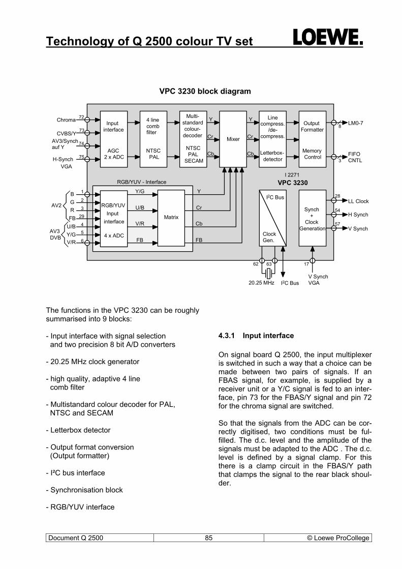
Technology of Q 2500 colour TV set
Document Q 2500 85 © Loewe ProCollege
The functions in the VPC 3230 can be roughly summarised into 9 blocks: - Input interface with signal selection and two precision 8 bit A/D converters - 20.25 MHz clock generator - high quality, adaptive 4 line comb filter - Multistandard colour decoder for PAL, NTSC and SECAM - Letterbox detector - Output format conversion (Output formatter) - I²C bus interface - Synchronisation block - RGB/YUV interface
4.3.1 Input interface On signal board Q 2500, the input multiplexer is switched in such a way that a choice can be made between two pairs of signals. If an FBAS signal, for example, is supplied by a receiver unit or a Y/C signal is fed to an inter-face, pin 73 for the FBAS/Y signal and pin 72 for the chroma signal are switched. So that the signals from the ADC can be cor-rectly digitised, two conditions must be ful-filled. The d.c. level and the amplitude of the signals must be adapted to the ADC . The d.c. level is defined by a signal clamp. For this there is a clamp circuit in the FBAS/Y path that clamps the signal to the rear black shoul-der.
LL Clock
LM0-7
FIFO CNTL
H Synch
V Synch
V Synch VGAI2C Bus
I2C Bus
Input interface
Synch +
Clock Generation
Clock Gen.
Matrix
Mixer
Y/G
U/B
V/R
V/R FB
FBU/B
AV3 DVB
AV2
Y/G
YB
RG
Cr
Cb
Y
Cr
Cb
Y
Cr
Cb
FB4 x ADC
AGC 2 x ADC
Output Formatter
Memory Control
4 linecombfilter
NTSC PAL
Multi- standard colour- decoder
NTSC PAL
SECAM
Linecompress.
/de-compress.
Letterbox- detector
RGB/YUV Input
interface
RGB/YUV - Interface
CVBS/Y
H-Synch VGA
AV3/Synchauf Y
Chroma
20.25 MHz
73
75
1
2
3
45
6
29
72
74
VPC 3230 block diagram
62 63 17
28
8
3
54
57
I 2271 VPC 3230
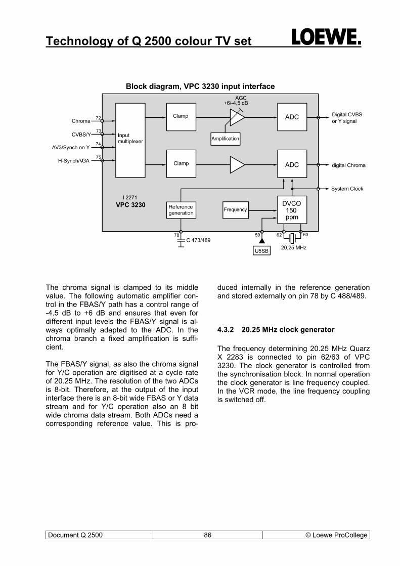
Technology of Q 2500 colour TV set
Document Q 2500 86 © Loewe ProCollege
The chroma signal is clamped to its middle value. The following automatic amplifier con-trol in the FBAS/Y path has a control range of -4.5 dB to +6 dB and ensures that even for different input levels the FBAS/Y signal is al-ways optimally adapted to the ADC. In the chroma branch a fixed amplification is suffi-cient. The FBAS/Y signal, as also the chroma signal for Y/C operation are digitised at a cycle rate of 20.25 MHz. The resolution of the two ADCs is 8-bit. Therefore, at the output of the input interface there is an 8-bit wide FBAS or Y data stream and for Y/C operation also an 8 bit wide chroma data stream. Both ADCs need a corresponding reference value. This is pro-
duced internally in the reference generation and stored externally on pin 78 by C 488/489.
4.3.2 20.25 MHz clock generator The frequency determining 20.25 MHz Quarz X 2283 is connected to pin 62/63 of VPC 3230. The clock generator is controlled from the synchronisation block. In normal operation the clock generator is line frequency coupled. In the VCR mode, the line frequency coupling is switched off.
CVBS/Y
H-Synch/VGAdigital Chroma
Digital CVBS or Y signal
AV3/Synch on Y
Chroma
System Clock
20,25 MHzU5SB
C 473/489
73
75
72
74
625978 63
Clamp ADC
AGC+6/-4,5 dB
ADC
DVCO 150 ppm
Amplification
Clamp
Inputmultiplexer
FrequencyReferencegeneration
Block diagram, VPC 3230 input interface
I 2271 VPC 3230

Technology of Q 2500 colour TV set
Document Q 2500 87 © Loewe ProCollege
4.3.3 Comb filter In this area of VPC the normally unavoidable Cross Colour and Cross Luminance interfer-ences in the PAL system are eliminated. In addition, the use of a comb filter even for colour transmissions permits the full 5 MHz Y resolution to be achieved. Without a comb filter it would be limited to approx. 3.8 MHz by the chroma trap, which would otherwise be required. This function can be switched off, as it is the case that for all receiver-side circuits for pic-ture improvement, even using a comb filter, there are some rare picture presentations which are not good. Switching off is imple-mented automatically via the analysis circuit. As this has error-free functioning, the user does not need to worry about switching off.
• Function of a comb filter Let us consider the transfer method of the PAL signal. The brightness information deter-mines that the full video bandwidth is not oc-cupied for all frequencies, but only in specific areas. The colour information is inserted into these energy gaps.
If the colour carrier is in one of these energy gaps, then all sideband frequencies are in the gap as well. For this the picture and colour carrier frequencies must be firmly coupled. The product of these two frequencies is an overlapping frequency. The sine waves cause light and dark pixels on the screen, which have a fixed position from line to line, so that on the screen these form a vertically placed light-dark pattern. The higher the colour car-
white
Clamplevel
black=
Klemm- pegel
Video
8-bi
t res
olut
ion
sych.
128
192
228
80
32
128
192
217
255
68
32
CVBS/Y Chroma
100%
ChromaBurst
75%
Chroma
A/D changer area for CVBS/Y and Chroma signal
BT FT

Technology of Q 2500 colour TV set
Document Q 2500 88 © Loewe ProCollege
rier frequency the less pronounced the Moiré becomes. In order to keep interference with the picture as low as possible, the phase position of the colour carrier frequency from line to line is shifted forward by 90°. In this way, bright and dark pixels only overlap after four lines. At normal distances the eye cannot detect this interference. This compensation is known as "Fourth Line Offset Procedure".
This fourth line offset now permits the filtering out of colour components from brightness in-formation, and the reverse. The phase shift from line to line causes a counter phasing of the colour carrier every two lines. If a two-line delay line is inserted into the cir-cuit and the direct and delayed signals are added together, the colour information is re-moved and the brightness information is pre-sent on the output at double the amplitude.
If one subtracts the two signals from one an-other, the brightness information is eliminated and the colour information is present at double the amplitude on the output of the circuit.
Theoretically this circuit supplies error free results. A condition for this, however, is the phase and amplitude equality of the chroma signal over 3 lines, which is only the case for the same and equally saturated colours. In practical terms picture joining can occur, in which cross colour and cross luminance inter-ference cannot be removed by the comb filter. Therefore, another circuit is integrated, in which three lines in sequence, from the point of view of both phase and amplitude, are compared. If a deviation is detected that goes beyond a specific difference, the comb filter function is automatically switched off and the separation of the two components is implemented tradi-tionally with chroma trap and band pass.
1. Zeile
2. Zeile
3. Zeile
4. Zeile
2 H delay
2 H delay
CVBS
Y
C
2 3 541
Chrominancebandpass
(PAL signal)
1 4
1 2
1 4
+
+
-
f
Y1
2 3 5MHz1f
Chroma1

Technology of Q 2500 colour TV set
Document Q 2500 89 © Loewe ProCollege
As VPC 3230 requires four lines to determine whether the comb filter is to be switched off, the filter operates more efficiently and more frequently than for a two line comb filter.
4.3.4 Multi-standard colour decoder This block executes demodulation for all TV standards - PAL, NTSC and SECAM. Addi-tional external components are no longer re-quired. On the output of the colour decoder there is an 8 bit wide luminance and chromi-nance signal respectively in 4:2:2 format. The VPC monitors the Auto S-VHS detection by means of the colour decoder for the sepa-rate chroma line of the colour burst. If signals are fed in from a VHS video recorder, then no burst is present on a separate chroma line. This is in turn communicated to the CCU. The CCU switches to VHS operation. If an S-VHS recorder is connected then a colour burst is measured on the chroma line on playback and the CCU switches the VPC to S-VHS opera-tion via the I²C bus.
4.3.5 Line compression and decompres-sion
To reproduce 4:3 pictures on a 16:9 c.r.t., and also for the various zoom modes, the video signal must be lengthened, or stretched, hori-zontally. For this the VPC 3230 has a line memory. Selection occurs at a slower speed, with the line beginning and end not being read (zoom, cinema) However, quicker selection is also possible. For this the start is delayed with respect to the deflection and the selection is ended before the line end of the deflection (4:3 and Pano-rama for the 16:9 c.r.t).
The vertical correction of the signal is achieved by the line interpolation in SAA 4991.
Letterbox detector For Cinemascope or other film standards up-per and lower black bars of various thickness are visible. These black bands can be re-moved by various zoom functions or at least reduced. Devices with 16:9 c.r.t.’s are also fitted with an automatic format conversion. Depending on the thickness of the black bars this automatic movie detection - AMD – switches between three different zoom modes. For this the Letterbox detector meas-ures the luminance and chrominance compo-nents in the upper and lower area. If, within defined lines, luminance and chromi-nance values of less than 10% are measured, the CCU switches the deflection controller and the display processor to the appropriate geo-metrical format. As programme logos are of-ten placed on the right and left of the black bars, no measurement takes place in this area. Automatic format conversion for 16:9 devices.
Write to52 s
Read from forCinema / Zoom
Line compression/decompression
Write to52 s
Read from for 4:3 / Panorama
on 16:9 c.r.t.s

Technology of Q 2500 colour TV set
Document Q 2500 90 © Loewe ProCollege
As 4:3 picture presentation with upper and lower black areas can lead to false results, the analysis occurs 4 sec. before switching oc-curs. If, however, undesired conversion proc-esses occur, the function can be switched off with the remote control.
4.3.6 Output format conversion
Up to now luminance and chroma signals have been processed IC internally at a cycle rate of 20.25 MHz. For additional processing by the 100 Hz Philips IC set, an output cycle rate of 13.5 MHz is required. In the Output Formatter, therefore, the output data is con-verted from 20.25 MHz to 13.5 MHz. The YUV output format is also converted at this stage to 4:2:2 and output by a multiplex procedure to 8 lines. The multiplex cycle rate must therefore have the double cycle rate of 13.5 MHz. The multiple cycle rate on pin 27 of I 2271/ there-fore has a frequency of 27 MHz.
4.3.7 Synchronisation block The synchronisation block generates all the synchronous, sampling, cycle and clamp sig-nals that are necessary for internal and exter-nal signal processing. Before the digital video signal reaches the horizontal and vertical synchronous separa-tion stage, it passes through a 1 MHz low-pass. With the low-pass, video and noise components >1 MHz are suppressed. All sig-nals that are required for the various process-
ing steps in the VPC are controlled via an in-ternal PLL stage and counter. No special synchronous signals are used for other external signal processing. The SAA4979 detects picture and line start from the data delivered by the VPC, and for further signal processing produces independent V/H synchronous signals. The VPC 3230 supplies the 27 MHz multiplex cycle to pin 27 for the digital luminance/chroma signals.
4.3.8 I²C bus interface Communication between C 161 and VPCm is via the I²C bus interface. The register in the VPC is loaded via this interface after start up and the status in operation is selected via it.
4.4 Half picture memory SAA4955HL The two memory IC's and the memory inte-grated into the SAA 4979 are functionally identical, their tasks , however, are different.
Number of linesin lower and upper area
Luminance /Chroma <10%
14 200 28 34 40
Zoom
Cinema
Panorama
4 : 3
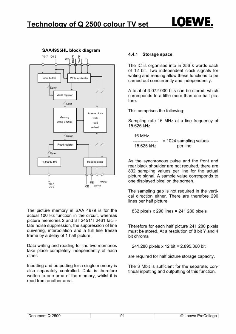
Technology of Q 2500 colour TV set
Document Q 2500 91 © Loewe ProCollege
The picture memory in SAA 4979 is for the actual 100 Hz function in the circuit, whereas picture memories 2 and 3 I 2451/ I 2461 facili-tate noise suppression, the suppression of line quivering, interpolation and a full line freeze frame by a delay of 1 half picture. Data writing and reading for the two memories take place completely independently of each other. Inputting and outputting for a single memory is also separately controlled. Data is therefore written to one area of the memory, whilst it is read from another area.
4.4.1 Storage space The IC is organised into in 256 k words each of 12 bit. Two independent clock signals for writing and reading allow these functions to be carried out concurrently and independently. A total of 3 072 000 bits can be stored, which corresponds to a little more than one half pic-ture. This comprises the following: Sampling rate 16 MHz at a line frequency of 15.625 kHz 16 MHz ----------------- = 1024 sampling values 15.625 kHz per line As the synchronous pulse and the front and rear black shoulder are not required, there are 832 sampling values per line for the actual picture signal. A sample value corresponds to one displayed pixel on the screen. The sampling gap is not required in the verti-cal direction either. There are therefore 290 lines per half picture. 832 pixels x 290 lines = 241 280 pixels Therefore for each half picture 241 280 pixels must be stored. At a resolution of 8 bit Y and 4 bit chroma 241,280 pixels x 12 bit = 2,895,360 bit are required for half picture storage capacity. The 3 Mbit is sufficient for the separate, con-tinual inputting and outputting of this function.
SAA4955HL block diagram
WE
Daten
Y0-7 C0-3
Y0-7C0-3
RST
W
SWC
K
OERE
RSTRSWCK
Memory
256k x 12 bit
Adress block
write
read
refresh
Write register
Read register
Read registerOutput buffer
Write controllerInput buffer
Data
Daten
Daten
IE

Technology of Q 2500 colour TV set
Document Q 2500 92 © Loewe ProCollege
4.4.2 Conversion of signals in 100 Hz in memory 1
Frequency doubling takes place in the half picture memory 1 (in I 2311), as it is read at double speed. This means it is possible to read the memory twice, whilst it is only written to once. The first reading of a half picture al-ways starts when a little over half the picture is in memory. Due to the double speed, writing to and reading out end at about the same time. As the return times at 100 Hz are also twice as fast, reading out starts before writing to. The picture is therefore read out for the second time and during this time up to half of the next half picture is written to memory.
4.4.3 Half picture memory 2 and 3 In this half picture writing to and reading out of memory take place at the same speed. The half picture is read to memory a second time and so delayed by a half picture. This means that half picture A can be written to and read from memory, whilst the same is happening in memory 1 for half picture B.
4.4.4 Control pulses The memory is controlled by the following pulses: pin 22: SWCK (Serial Write Clock) Cycle for reading in the Y/C signals to the memory. pin 23: RSTW (Reset Write) The address counter for writing at the start of the memory area is set at H level.
50/100Hz write/read cycle
1. Half picture 2. Half picture 2. Half picture
50HzIndicator
50Hz Indicator
50Hz Indicator
50HzIndicator
50HzIndicator
50HzIndicator
100Hz Indicator
100Hz Indicator
100Hz Indicator 100Hz Indicator
100Hz Indicator
100HzIndicator
Centre ofpicture
100%1. Half picture
1.Half picture1x read from
Start 1st Halfpictureread
2. Halfpicturepicturestart
1. Half picture2.x read fromMemory content
1. Half picture
50% 2. Half picture
50% 1. Half picture
1.Half picture2x read from
50% 2. Half picture
50% 1. Half picture
Start 2.Half picture1.x read from
100%2. Halbbild
2.Half picture1x read from
50%1.Half picture

Technology of Q 2500 colour TV set
Document Q 2500 93 © Loewe ProCollege
pin 24: WE (Write Enable) So long as H level is present, the address counter continues counting to write with WCK. pin 25: IE (Input Enable) Data inputs for Y/C signals are released at H level. pin 30: OE (Output Enable) Data outputs for Y/C signals are released at H level. pin 21: RE (Read Enable) So long as H level is present, the address counter continues counting to read with RCK. pin 32: RSTR (Reset Read) H level sets the address counter to read at the start of the memory area. pin 33: RCK (Read Clock) Cycle for reading the Y/C signals from the memory.

Technology of Q 2500 colour TV set
Document Q 2500 94 © Loewe ProCollege
Hal
f pic
ture
mem
ory
I217
1SA
A49
55H
L
output
input
Dat
aD
ata
RE
RST
RSR
CK
OE
Hal
f pic
ture
mem
ory
I216
1SA
A49
55H
L
output
input
Dat
aD
ata
RE RSTR
SRCK
OE
IEWE
RSTW
SWCK
Hal
f pic
ture
mem
ory
2.9M
bit
I245
1SA
A49
55H
L
output
input
Dat
aD
ata
RE
RST
R
SRC
K
OE
IE WE
RST
WSW
CK
I246
1SA
A49
55H
L
output
input
Dat
aD
ata
RE
RST
R
SRC
K
OE
IE WE
RST
W
SWC
K
I227
1V
PC32
30M
AIN
I242
1SA
A49
93FA
LCO
NIC
I215
1V
PC32
33PI
P
106
2414
31
146
2431
134
140
3223
2332
2525
U3.
3U
3.3
6053
81 84
25V
D
136
HD
54
HD
55
VD
83IE
62
32M
Hz/
Clo
ck
3322
3322
79
32M
Hz/
Clo
ck
32M
Hz/
Clo
ck
6
5320
IEWE
RSTW
SWCK
25 2524 24222227 21
2323
32 3233 333130 30 31
1827
218
Q2500/H memorycontrol
16/28
53 42
3
RSTR27MHz/Clock
Interlace Output - 0=Field 1/1=Field 2
Y/C Output Enable
Inte
rlac
e O
utpu
t - 0
=Fie
ld 1
/1=F
ield
2
Writ
e E
nabl
e
RSTR
Clo
ck/
27M
Hz
Interlace Output/PIP0=Field 1/1=Field 2
Rea
d En
able
Out
put B
us A
Read EnableOutput
Input Enable
Reset Read/Write
Read Enable
Writ
e E
nabl
e
RE
Hor
izon
tal R
efer
enz
Inpu
t
Bus
A
Bus
B
Bus
CB
us D
Bus
EFAY0-7 / FAC0-3
3Y0-
7/3C
0-3
4Y0-
7/4C
0-3
5Y0-
7/5C0
-3
6Y0-
7/6C
0-3
7Y0-7/7C0-3
2L0-
7/2C
0-3
7L0-
7/7C
0-3
1LC0-71LM0-7
1LM
0-7
1LM
0-7
1LS0
-7
I231
1SA
A49
79H
+B
ESI
C
Hal
bbild
-sp
eich
er 3
,5M
bit
Hal
f pic
ture
mem
ory
2.9M
bit

Technology of Q 2500 colour TV set
Document Q 2500 95 © Loewe ProCollege
I246
1SA
A49
55H
L
output
input
Dat
aD
ata
RE
RST
R
SRC
K
OE
IE WE
RST
W
SWC
K
I227
1V
PC32
30M
AIN
I242
1SA
A49
94R
AV
EN
1431
14624
134
14023
32
25U
3.3
6053
81 84
25V
D
136
HD
54
HD
55
VD
83IE
62
32M
Hz/
Clo
ck
3322
79
32M
Hz/
Clo
ck
32M
Hz/
Clo
ck
1827
21
Q2500/M memorycontrol
16/28
53 42
3
RSTR27MHz/Clock
Interlace Output - 0=Field 1/1=Field 2
Y/C Output Enable
Interlace Output/PIP0=Field 1/1=Field 2
Rea
d En
able
Out
put B
us A
Read EnableOutput
Input Enable
Reset Read/Write
Read Enable
Writ
e En
able
RE
Hor
izon
tal R
efer
enz
Inpu
t
Bus
A
Bus
B
Bus
CB
us D
Bus
E
FAY0-7 / FAC0-3
3Y0-
7/3C
0-3
4Y0-
7/4C0
-3
7Y0-7/7C0-3
2L0-
7/2C
0-3
7L0-
7/7C
0-3
1LC0-71LM0-7
I231
1SA
A49
79H
+B
ESIC
Hal
f pic
ture
mem
ory
3,5
Mbi
t
Hal
f pic
ture
mem
ory
2.9M
bit

Technology of Q 2500 colour TV set
Document Q 2500 96 © Loewe ProCollege
4.5 Falconic module SAA 4993 With the conversion of a picture signal to a line coupled sampling and level adaptation at 3.3 V, 100 Hz is achievable with a 3 Mbit pic-ture memory and a memory controller As doubling of the picture change frequency, depending on picture quality and picture pres-entation, can lead to undesired side effects, a number other features are provided on the Q 2500 chassis. This means that the side effects can be compensated for.
4.5.1 Noise reduction Together with a second picture memory, SAA 4993 is able to eliminate some of the picture noise that occurs owing to an inadequate an-tenna signal. Internally the IC has two separate signal paths, one for the Y and one for the chroma signals. Functionally they are both identical. In the chroma path is a demultiplexer on the in-put and a multiplexer before the output.
I227
1V
PC32
30M
AIN
1827
21
Q2500/B memorycontrol
16/28
53 42
3
RSTR
27MHz/Clock
Interlace Output - 0=Field 1/1=Field 2
Y/C Output Enable
1LC0-71LM0-7
I231
1SA
A49
79H
+B
ESIC
Hal
f pic
ture
mem
ory
3.5
Mbi
t

Technology of Q 2500 colour TV set
Document Q 2500 97 © Loewe ProCollege
Simply expressed the noise suppression sys-tem consists of the current half picture signal, in which components of the previous signal are mixed. The composition of the output sig-nal, that is the number of components of the direct and the number of components of the delayed half picture, are determined by the so-called K factor. This K factor is determined by integrated automation. When using the automation the K factor is dependent on the movement between the half pictures. If there is a lot of movement, noise suppression is not very effective.
* (SAA 4994 does not control FM3)
SAA 4993 block diagramYB
VA
YC YD YE
FM3*FM2
Sequencer
Decompr.Compress.
mux
Vec.
Vec.Pi
x-Pe
ak
Ver
t. Pe
akin
g
Rig
ht M
PR
AM
Left
MPR
AM
Deinterlager
Motion Estimator
Unconversion
mux
YF
YGTPM ESM
Vert. Zoom
SPM
DNR
Control
P Interface
PDA
PCL
Setting
K factor
DNR Y
Principle noise suppression
Picturememory
2
Y K
1- K
+

Technology of Q 2500 colour TV set
Document Q 2500 98 © Loewe ProCollege
Information about the size of movement is provided by the movement detection. This occurs only in the Y branch, with which the K factor is set simultaneously for chroma and Y. The drawing shows the DNR principle for the Y path. As already mentioned the circuit in the chroma path is identical. The K factor can have a value from 0 to 1. At K = 1, 100% of the direct signal and 0% of the delayed signal is switched to the following "And". No noise suppression is therefore available.
In the other extreme case K = 0, only the de-layed signal would be switched, which would correspond to a freeze frame. To avoid this the K factor in our TV sets can never be 0. Otherwise it would only be programmes with a weak signal that would be incapable of being displayed.
4.5.2 Line interpolation The line interpolations circuits allow a situation to be achieved in which a full-line picture is written for PALplus signals . The advantage with respect to a PALplus decoder is that even without a PALplus signal, the interpolation in all zoom modes delivers a full-line picture. This function is explained in the following paragraphs for PALplus, in the zoom functions the circuit operates similarly only with other factors.
A standard PAL signal consists of 576 visible lines. For PALplus, 144 of the lines are dark sampled and only 432 lines are transferred as a visible picture. In 16:9 c.r.t’s these signals are shown in the ZOOM mode. In order to display 576 lines the information for 4 lines must be determined by 3 lines respectively. This computer operation is very
complicated and will therefore not be ex-plained here. Line interpolation must be carried out both in chroma as in the Y branch.
K factor
K factor
0,75
0,50
0,25
1
00 > 0 Noise
level
Standard PAL signal PALplus signal
Interpolation
PALplus signal on 16:9- c.r.t. with line interpolation
576 linesvisible picture
576 lines visible picture
432 lines visible picture
72 lines black bar
72 lines black bar

Technology of Q 2500 colour TV set
Document Q 2500 99 © Loewe ProCollege
4.5.3 Movement detector In the Y branch there is a movement detector. Here current and previous half pictures are compared with each other. An assessment is made of whether it is a question of full pictures in Cinema Scope format. The CCU receives this information via the microprocessor for the Automatic Movie Detection (AMD). The movement detector is also responsible for the setting of the noise suppression K factor. In addition, using the movement from the pre-vious to the current half picture an assess-ment is made of how the movement between the two half pictures could behave. In this way, in the movement compensation stage immediately following a new half picture can be calculated. At the same time it must be taken into account that the two half pictures, contain the intermediate lines for the other half picture respectively. In this way a continuous process of movement over all half pictures is achieved, both for horizontal as well as verti-cal movements. The DMI (Digital Moving In-terpolation) function is active for both full pic-ture presentation and for standard video sig-nals. The operation of this switch is largely error free. Nevertheless, under unfavourable condi-tions negative effects can occur, therefore the DMI function can be switched off. Instead, the DLC (Digital Lineflicker Control) function is switched on.
4.5.4 Memory control Control of the SAA 4993 is implemented via the µP interface from I 2311. The µP bus is assigned to pins 26 (DA) and 27 (Cl). In addi-tion it is here in conjunction with the Memory Controller that writing to the 2nd picture mem-ory and reading from the two memories is de-termined.
4.6 SAA 4979 (BESIC) The next IC in the signal path, the SAA 4974, is designed for the following functions. - Demultiplexer for luminance/chroma sepa-
ration - 3.5Mbit memory for 50/100Hz conversion - Cycle rate converter from 27MHz to
32MHZ − Two signal paths for the separate process-
ing of the Y and chroma signals
− Demultiplexer for the chroma signals
− Band width doubling and digital CTI circuit for improved colour transfer
− Peaking circuit Y branch to increase picture sharpness
− Three blank stages for dark sampling
− Three 10 bit DACs for the generation of
analogue R-Y-, B-Y- and Y-signals, I²C bus interface and timing control for the control of the individual processes through the microprocessor.
− Microprocessor bus for the control of the
SAA 4993. − Control of write and read processes in the
half picture memory, as well as the total digital 100 Hz video signal processing.
− Generation of a 32 MHz cycle.
− Generation of H and V synchronous pulses for the TDA9332 video/deflection proces-sor.

Technology of Q 2500 colour TV set
Document Q 2500 100 © Loewe ProCollege
4.6.1 Chroma branch In the design of the colour television transmis-sion the compatibility with normal black/white systems must be observed, in order for colour transmissions to be received by black and white sets. For this reason the colour informa-tion must be integrated into the available fre-
quency spectrum used for the brightness in-formation. Secondly, to prevent interference the band-width for the colour signal must be kept as narrow as possible. For this reason a band-width of only 1.2 MHz was selected and the carrier frequency set at 4.43 MHz.
DNCmovement
determinationBlack Bar
determination
ITU 656Decoder 1
ITU 656Decoder 2
Main Channel
Sub Channel
Fast Switch
DynamicNoice
Reduction
FieldMemory3,5 MBit
Sample Rate Conversion
27 to 32 MHz
DownSampling
UPSampling
PanoramicZoom
Luminance
Chrominace
PeakingY-Delay
Demultiplexerbandwidth
doublin4:4:4
Digital colouredge
sharpening
Triple
DAC
10Bit
Systemcontrol
µP - Interface
I2C-Bus
µP-Bus
Y
U
V
LM0-7
27 MHz
2L0-72C0-3
7L0-77C0-3
SourceSelect
Bypass
Bypass
I2311SAA4979H
8/
8/
16/
16/
16/
8/
16/
16/
Y
U/V
10/
10/
10/
Speicher-steuerung
32 MHz

Technology of Q 2500 colour TV set
Document Q 2500 101 © Loewe ProCollege
Owing to the narrow bandwidth the rise times for colour change are very long, which ap-pears on the screen as "washed out" transi-tions.
To compensate for this deficiency, two circuit components are incorporated into the SAA 4979, with which short rise times can be achieved artificially, thereby improving the colour transitions. In the circuit before these components is a demultiplexer, with which 8-bit wide parallel R-Y- and B-Y signals respectively are derived from the supplied signals.
4.6.2 Band width doubling In order to increase the effectiveness of the colour flank increase on the supply side, a doubling of the bandwidth from 4:1:1 to 4:2:2 is implemented. Using a linear phase interpolation filter addi-tional sampling values are calculated from the available chroma sampling values. These calculated sampling values are inserted respectively between two available values, by which means the bandwidth is doubled. In this way, steep flanks can be transmitted more easily.
4.6.3 Colour flank sharpening An improvement of the colour transition is achieved by a dual differentiation of the origi-nal chroma signal and the ensuing subtraction of the derived correction signal of the chroma signal. The changes in these signals are evaluated in separate circuits for U and V, and if a thresh-old value specified by the software is ex-ceeded a correction value is calculated. After the two derived correction signals have been cleaned of noise components, they are sub-tracted from the available chroma signals U and V. The subtraction is implemented by in-version of the correction signals and subse-quent addition with the original signal. To avoid colour phase errors by the over-shooter, it must be blocked by limiter stages. Here analogue signals are produced from the respective 8-bit wide digital R-Y and B-Y sig-nals, which are then output at 1.8 Vss on pins 46 and 48.
4.6.4 Y signal path The peaking circuit is not used. The signal is led directly to the sampling stage. This oper-ates in the same way as the sampling stage in the chroma branch.
t
a)
Uin, Vin
t
b)
Ampl.
t
t
d)
Uout, Vout
a) U, V input of SAA b) U, V Correction signal c) U, V input + Correction signal d) sharpend and limited U, V
c)
Ampl.
Technology of Q 2500 colour TV set
Document Q 2500 102 © Loewe ProCollege
Via the sampling circuit, the digital Y signal, which is now 9-bits wide, reaches a DAC, which generates an analogue signal. This is then output on pin 44 at 1.5 Vss.
4.6.5 Microprocessor interface All processes in the SAA 4979 are controlled by SDA6000 via the I²C bus 0 (pin 1 = SDA, pin 2 = SCL). In addition, information for the SAA 4993 and the memory control is also transferred. The SAA 4993 is controlled by the BESIC via the microprocessor bus to pins 108 (µP DA) and 107 (µP CL). Switching outputs 4 are used for the switching of the VGA synchronisation. If a switch is made to the VGA programme location, then pin 4 is switched from I 2311 to L level. With this logic state the vertical synchronous pulse of the VGA interface W 1011 pin 4 is switched directly to the video/deflector controller I 2521 via the four Nand gates I 2361 A/B/C and D. The VGA synchronous pulse is, in addition, monitored by I 2271 on its pin 17. If no syn-chronisation or false synchronisation is de-tected, I 2311 resets its output on pin 4 and thereby switches over to internal V synchroni-sation.
4.6.6 Control of the 100 Hz processing (Display) This stage synchronises the read out from the half pictures and the writing to memory in the second memory. As the signals in the SAA 4993 are written to and read out, it has direct control and is only synchronised by the BESIC. Via pulse RE (pin 84) the Falconic module controls the reading from both half picture memories and the writing to the second mem-ory. With pulse IE (pin 83) SAA 4979 controls the data inputs in the second half picture memory. With L level a switch can be made to freeze frame, for example.
Furthermore, the display stage gives a hori-zontal pulse on pin 54 and a vertical synchro-nous pulse on pin 55 for the synchronisation of the deflection in TDA9332. At the same time, the vertical pulse VD acts as a reset for the Falconic and the half picture memories, for resetting the address counter on reading from the memory and for writing to the second memory.
4.7 Video/deflection processor TDA 9332/Range Video/RGB path
The last IC for picture signal processing, apart from the RGB output stages, is the TDA 9332. It also controls the deflection stage. Inputs for analogue R-Y, B-Y and Y signals: - Two RGB inputs for analogue signals from
the CCU and the VGA interface and/or pic-ture in picture generation
- Matrix circuits for RGB generation from the
difference signals - Signal selection for the switching of the
required RGB signals - Y and colour difference matrix for the gen-
eration of Y and difference signals from the selected RGB signal
- Hue control for NTSC operation and
gamma correction in the Y branch - Saturation, contrast and brightness setting

Technology of Q 2500 colour TV set
Document Q 2500 103 © Loewe ProCollege
- RGB driver stages - Beam current limiter circuit - Automatic cut off control - I²C bus interface and control register - DAC for programmable d.c. voltage − PLL for generation of cycle frequency − Control block for the synchronisation of the
output stages − DAC for O/W, V control and H output stage − Beam current dependent correction of the
vertical and horizontal amplitude and beam current dependent H phase correction.
− Horizontal start up control
− I²C bus interface
4.7.1 Matrix circuits and signal selection The R-Y, B-Y and the Y signals are fed to the IC via pins 26, 27 and 28. The green compo-nent is recovered and the RGB signals pro-duced using two matrix circuits, one after the other. These RGB signals are fed to a selection cir-cuit, to which the RGB signals from the CCU via pins 2, 3 and 4 and from the VGA-interface via pins 35, 36 and 137 are also fed. With this circuit the required signal is selected or two signals mixed together.

Technology of Q 2500 colour TV set
Document Q 2500 104 © Loewe ProCollege
MG
R44
5
Y
Y
UV
SAT
CO
NTR
U VM
ATR
IX
R G B
R G B
R GG
B
BRIw
hite
poin
tR BBL
UE
STR
ETC
H
40 41 42
28 27 26
YIN
UIN VIN
LIM
ITER
44
30 31 32
RI1
GI1 BI1
H-S
HIF
T
1043 1125
18 6 1917 739
DEC
BGG
ND
1
GN
D2
23
V P1
DEC
VDV P2
2021
1314
2215
16VS
CI re
f
124
3
E-W
GEO
MET
RY
GEO
MET
RY
CO
NTR
OL
24 12H
SEL
3329
3837
3635
34
TDA9
332
I252
1
BL1
FBC
SOBL
2G
I2R
I2PW
LBI
2
BCL
BOGO
RO
BLKI
N
DAC
OU
T
SDA
SCL
VDO
A
589
VDO
BEW
OEH
TIN
XTAL
IXT
ALO
LPSU
FLAS
HH
OU
T
SCO
HFB
DPC
HD
V D
SWIT
CH
SATU
RAT
ION
CO
NTR
OL
CO
LOU
RD
IFFE
REN
CE
CO
NTR
AST
CO
NTR
OL
RG
BIN
SER
TIO
N
WH
ITE
POIN
TAN
DBR
IGH
TNES
SC
ON
TRO
L
OU
TPU
TAM
PLIF
IER
AND
BUFF
ER
RG
B-YU
VM
ATR
IXBL
ACK
STR
ETC
H
PWL
AND
BEAM
CU
RR
ENT
CO
NTI
NU
OU
SC
ATH
OD
EC
ALIB
RAT
ION
SUPP
LYSO
FTST
ART/
STO
PLO
W-P
OW
ERST
ART-
UP
H/V
DIV
IDER
6-B
IT D
ACs
19 ́
2 ́ 4
-BIT
DAC
sI2
C-B
US
TRAN
SCEI
VER
CLO
CK
GEN
ERAT
ION
AND
1st L
OO
P
PHAS
E-2
LOO
PH
OR
IZO
NTA
LO
UTP
UT
RAM
PG
ENER
ATO
RVE
RTI
CAL
GEO
MET
RY
12M
Hz

Technology of Q 2500 colour TV set
Document Q 2500 105 © Loewe ProCollege
According to the operating mode selection is either with H level on blank on pins 38 and 33 or controlled from the computer via the I²C bus. In the following section of the circuit Y and colour difference signals are generated from the RGB signals.
4.7.2 Control stages In the Y path the first component is a circuit for gamma correction and in the colour differ-ence branch the colour saturation setting stage. After RGB has been generated again from the difference signals and the Y signal, the setting stages for contrast and brightness are reached. The control stages for contrast and colour saturation in the other IC's are set to maxi-mum and have no function. There is, in addi-tion, in each channel, a setting stage for the white value, and the black value is set with the amplifier stages that follow. The white value and the basic setting of the black value are determined in the two corre-sponding positions of the service mode. In further a operation the black value is deter-mined by the cut off control. The RGB signals are output at a maximum of 3.5 Vss via pins 40, 41 and 42. The measured values for cut off and leakage current are fed to the IC on pin 44. With the evaluation circuits for leakage current and cut off, together with the computer, subsequent adjustment is carried out via the output ampli-fier, in order to keep the picture impression stable independently of aging. Pin 43 is connected to the base of the diode split transformer. The circuit integrated into the IC thereby receives information about the beam current flowing into the c.r.t.
If the maximum permissible value is exceeded there, the circuit reduces the contrast and the brightness with the corresponding control stages. (see basic board “Beam current limita-tion“).
4.7.3 I²C bus interface and raster correc-tion
All control processes such as brightness, con-trast, etc are controlled via pins 10 and 11 of the I²C bus interface. In addition, a DAC can also be controlled via the I²C bus. For this, TDA 9332 on pin 25 outputs an adjustable voltage. This is fed to the rotation panel on pin 3 of connector W 1021. At this point an addi-tional coil on the tube turns the deflection raster, thus providing compensation of the earth’s magnetic field at the installation site of the device. The value of the raster correction can set in both service mode and in the menu for picture functions. If the device is turned, the influence of the earth’s magnetic field changes. The planned rotatable rack takes this into account. The rack is controlled from the chassis, with the rotation angle being determined by the TV software. Raster correction can also be de-termined, in that on rotation the voltage on pin 26 of TDA 9332 is changed. The influence of the rotation angle on the raster displacement is almost linear. On instal-lation of the device, it is sufficient for correct functioning of the correction to input a value for raster correction into the EAROM for the centre and the two end stops.
4.8 Picture in picture On the signal board an optional picture in pic-ture circuit is possible. This circuit consists of the video processor

Technology of Q 2500 colour TV set
Document Q 2500 106 © Loewe ProCollege
VPC 3233 /I 2151 and the PIP memory I 2161/71 The video processor PIP is the same IC type as the main video processor I 2271. With the VPC 3233 various PIP representa-tions are possible. Our device controls support 3 PIP representations.
Split Screen The screen is split into two halves. On the left side the half picture is displayed and on the right side the picture of the PIP electronics. Both pictures are the same size and quality. In the horizontal level, sections of a picture on the left and right are naturally cut off. The core area, however, is correctly displayed.
PIP small The picture in picture, which is reduced to 1/9 of its normal size, can be positioned in any of the four corners.
PIP large The same is true as for PIP small, only the size is 1/4 of the normal picture. For 4:3 devices Split Screen is not possible. For small and large PIP display the PIP pic-ture must be correspondingly compressed.
This occurs at the vertical level by the interpo-lation of picture lines. For the small setting, 3 lines are compressed and for large setting 2 lines, and for each a new line is calculated by interpolation. In the horizontal level these lines are then compressed accordingly. The writing of the picture in picture data to the PIP mem-ory is controlled completely by the PIP-VPC. Reading from memory is controlled fully from the main VPC. Writing to and reading from memory is there-fore independent. There is no synchronisation between the two VPC’s. The PIP processor processes FBAS as well as Y/C signals. The video transfer applies the FBAS/Y signal to pin 73 and the associated chroma signal to pin 72. All possible signal sources can therefore be displayed as PIP. If an online module is integrated into the TV set, the picture can also be displayed by the online module as PIP. The Y/C signal from the online module reaches the pin connector W 1531 on the signal board. The TVO/Y signal is applied to pin 74, and the associated chroma signal to pin 71 of I 2151. For the basic and medium signal board vari-ants a single chip PIP processor SDA 9488 is used.

Technology of Q 2500 colour TV set
Document Q 2500 107 © Loewe ProCollege
SDA
948
8x /
PiP-
Proz
esso
r
Q
2500
M/B
RG
B M
atrix
Peak
ing
Ove
r-sa
mpl
ing
Inse
rtio
n
eDR
AM
512k
bit
Fram
eG
ener
atio
n
Dis
play
Con
trol
ler
Pare
ntSy
ncPr
oces
sing
Clo
ckSy
nthe
size
r
Mem
ory
Con
trol
ler
Ske
wco
mp.
H/V
Sca
ler
Dec
imat
ion
Col
orD
ecod
erPA
L/ S
ECAM
/ NTS
C
Y/C
and
Sync
Sep.
Inse
tSy
ncPr
oces
sing
Inpu
tSe
lect
Cla
mp
Gai
n
DEMUX
Dat
a Sl
icer
Acq
uisi
tion
Con
trol
ler
MUX
TRIP
LEAD
C3x
8bit
1)
Trip
leD
AC 3x
7bit
IN1
IN3
FSW
OU
T1O
UT2
OU
T3SE
L
Fast
RG
B/Y
UV
Switc
h
IN2
VDD
A2VS
SA2
VDD
VSS
CVB
S1C
VBS2
CVB
S3
VREF
H
VREF
L
VDD
A1VS
SA1
XIN
XQI2
CSC
LSD
AH
SPVS
P
VREF
M
XTAL
20.2
5 M
Hz
INTR
28 26 24252127
2223
1920
10
1516171814131211
DCVBS/DY
DUV/DCHR

Technology of Q 2500 colour TV set
Document Q 2500 108 © Loewe ProCollege
With this module the PIP function can be used with our devices. Split screen and Multi PIP are not used. This processor does not form part of the digi-tal signal processing. As you can see from the circuit diagram, the RGB signals from SDA 9488 pins 15/16 and 17 are fed directly to TDA 9332 (pins 30/31/32). SDA 9488 receives the FBAS or Y/C signal to be processed on pins 26/28 from the video-conversion IC. The necessary 100 Hz V/H synchronous sig-nals are fed to pins 4 and 3. For our medium devices as for our high vari-ant a VGA interface can be retro-fitted. The VGA RGB signals are not, however, fed di-rectly into the TDA 9332, as in the high-end device, but for VGA operation are looped through the SDA 9488 to the TDA 9332. From the VGA interface the RGB signals are led to pins 11/12 and 13 of SDA 9488.
4.9 Video/deflection controller TDA9332 (deflection area)
The Philips TDA 9332 video/deflection control-ler can be used in standard TV’s as well as in devices with double picture and line fre-quency. The video/deflection controller is switched in the Q 2500 chassis in such a way that it can drive the H/V deflection with double the fre-quency.
4.9.1 Clock generation/Phase 2 loop All the necessary cycle and synchronous sig-nals necessary for internal signal processing are derived from this block. The synchronous signals generated by SAA 4979 are fed to pin 24 (H synchronous signal) and to pin 23 (V synchronous signal) of the controller. The cycle frequency for the video/ deflection processor is produced with an ex-ternal 12 MHz quartz on pins 20 and 21. This cycle is synchronised by a PLL that operates with the horizontal synchronous pulse HA.
4.9.2 DAC for OW/V control and H output stage The DACs for the two vertical -VD+ control signals contain all vertical correction informa-tion. The VD+ control signals are output to pins 1/2 and are fed via R 1032 and R 1033 to pins 2/3 of W 1511. In this way the V output stage on the basic board is controlled by d.c. The vertical frequency E/W parabola also con-tains all correction information. The control signal is output by I 2521 on pin 3 and is fed via W 1511 pin 6 to the basic board. In this way the E/W output stage on the basic board is controlled. The horizontal output is programmed in such a way that on pin 8 a rectangular signal with 13 µs H and 19 µs L level for control of the H-output stage on the basic board is output. The signal reaches Q 2556 and Q 2561 on pin 13 of pin connector W 1511 via two inverter stages and controls H output stage Q 534 on the basic board via H driver stage Q 526. In the SAT standby, for SAT radio and for overwriting in standby, the c.r.t. must be switched off. For this the horizontal pulse is switched off via transistor Q 2951. The control of Q 2951 is implemented via pin 79 of the SDA 6000 microprocessor. The c.r.t. is switched off here with H level.
4.9.3 Beam current dependent correction the vertical/horizontal amplitude and the H phase As we know the high voltage at the anode connection of the c.r.t diminishes at high beam currents, owing to the internal resis-tance of the high voltage generation. The lower high voltage means that the beam of electrons is not so strongly accelerated and can be deflected outwards again by the V/H magnetic deflection fields. The picture be-comes larger. If the beam current decreases (darker picture content) the picture becomes smaller again. Appropriate corrective measures are neces-

Technology of Q 2500 colour TV set
Document Q 2500 109 © Loewe ProCollege
sary to prevent this video pumping or at least to reduce it. To do this beam current depend-ent correction information is applied to pins 4 and 14 of the deflection controller . The OW and V amplitude are influenced via pin 4 and the H phase via pin 14. The beam current dependent information taken from the base of the diode split trans-former and output by W 1511 via resistances and the two transistors Q 2639/Q 2638 is fed to pin 4 and pin 14 of TDA 9332. Switching via these two transistors ensures that the base voltage is adapted in an optimum way to I2521. pin 4/14 of I 2521 requires a voltage from 1.2 V to 2.8 V. The vertical amplitude compensation is defined firmly in I 2521 and is the same for all types of c.r.t. The horizontal amplitude compensation is influenced via in-ternal registers by I 2521. Various values are held in EAROM for the various c.r.t types. Dependent on the measured values the pic-ture width and, if necessary, the V amplitude are influenced by the E/W output. Delay of the control is about the duration of 10 lines. A lat-eral glitch at bright picture settings cannot be avoided but can be reduced to some extent. Due to the varying load on the line output stage, the line flyback pulse is also affected. This means that beam current changes also influence the H phase. The correction informa-tion on pin 14 of TDA 9332 opposes this via the internal phase correction.

Technology of Q 2500 colour TV set
Document Q 2500 110 © Loewe ProCollege
5 Audio signal processing
5.1 Audio-Signal path Block diagram Q 2500 H/M and B
14
5
13
25
12
4
15
24
16
6
17
23
1615 54
53
1314
1112
254
1019
920
1118
623
I185
1TE
A64
20D
I187
1TE
A64
22D
I205
1M
SP34
11A
C3
mod
ule
AV1 Pin 6
AV1 Pin 2
AV2 Pin 6
AV2 Pin 2Front/W1521/4Front/W1521/2
DVB/Sat/W1506/4 DVB/Sat/W1506/2
MSP Pin34
MSP Pin33
209
AV3 Pin2
AV3 Pin6
524
(DVB2 W1416/2)
(DVB2 W1416/4)
AV2 Pin3
AV2 Pin1
AV1 Pin3
AV1 Pin1
AV3 Pin1
AV3 Pin3
3637
RW
2091
/4W
2091
/5
L
LR
30
28 L
27
R
LC
W20
91/6
RC
W
2091
/7
##
C20
82C
2084
5 6 7
I2S-
WS
I2S
- DA
out1
I2S
- DA
in1
W20
71/6
W20
71/8
W20
71/8
W20
91/1
LFE
W2091/2
RS
W2091/3LS
W2091/8
C
W16
10/1
W16
10/2
RC
LC
Basi
c-B.
24R
25L
W1431/HF transmitter
LSRS
R
L
8 6 4 2
Headphones
W15
21
10 11
47 48W
1421
/2 /
TVO
W14
11/1
/ Au
dio
anlo
g
W14
11/3
/ Au
dio
anlo
g
W14
21/4
/ TV
O
50 51 67 68 69
W12
11/1
1 IF
tune
r
W12
11/1
2 IF
ear
th
W14
16/4
IF T
win
_Sat
W12
11/1
0 Se
cam
/L M
ono
60
Q2500/H/Maudio signalpath
5756
3334
I209
1/D
I209
1/C
I209
1/B
Q1441/46
Q14
61/6
6
KH
KH
W15
41
24
H-L
ink
W12
51/2
DVB
-int.
SPD
IF in
D
VB in
t.
W20
91/1
0
W20
91/1
2
W20
91/1
4
W20
91/1
1
SPD
IF in
1
SPD
IF in
2
SPD
IF o
ut
L R L R
LR
RL
RL
LR
# Not
equi
pped
with
AC
3
L1R
1
L1R
1
R2
L2
R2
L2
R3
L3
R3
L3
C20
74#
C20
91
#
C20
92#

Technology of Q 2500 colour TV set
Document Q 2500 111 © Loewe ProCollege
Fron
t LS
1413
1215
1617
5453
254
1019
920
1118
623
I187
1TE
A642
2D
I205
1M
SP34
11
AV1 Pin 6
AV1 Pin 2
AV2 Pin 6
AV2 Pin 2Front/W1521/4Front/W1521/2
DVB/Sat/W1506/4 DVB/Sat/W1506/2
MSP Pin34
MSP Pin33
524
(DVB2 W1416/2)
(DVB2 W1416/4)
AV2 Pin3AV2 Pin1
AV1 Pin3
AV1 Pin1
3637
RL
28 L
27
R
C20
82
C2084
W16
10/1
W16
10/2
RC
LC
Basi
c-B.
24R
25L
Hea
dpho
nes
W15
21
10 11
67 68 69
W12
11/1
1 IF
tune
r
W12
11/1
2 IF
ear
th
W14
16/4
IF T
win
_Sat
W12
11/1
0 Se
cam
/L M
ono
60
Q2500/Baudio signalpath
3334
I209
1/D
I209
1/C
Q14
41/4
6
Q14
61/6
6
KH
KH
RL
RL
LR
L1R
1R
2L2
R3
L3

Technology of Q 2500 colour TV set
Document Q 2500 112 © Loewe ProCollege
In the Q 2500 chassis a family of multi-standard sound processors is used, which contain all the modules for digital sound/IF-processing, FM/Nicam signal demodulation, Nicam decoding and audio base band. The multi-standard MSP 3411 sound processor is manufactured in 1.0 µm CMOS technology and incorporated into the Q 2500 chassis in a 80 pin PLCC housing. For devices without NICAM an MSP 3400 or 3401 is used, which cannot process these NICAM signals. The MSP 3401 and MSP 3411 also support virtual surround. Otherwise there is no difference between these three types. The multi-standard sound processor can be roughly divided into a demodulator-decoder-block and into an area that is responsible for the digital audio base band processing - DFP.
The following functions are integrated into the two blocks.
5.2 Demodulator/Decoder-Block − Two selectable inputs for the sound/IF sig-
nal − Automatic amplification control (AGC) for
the selected sound/IF signal − A/D converter for the sound/IF signal − Two internal sound/IF channels, e.g. for
stereo with sound carrier 5.5 MHz /5.74 MHz
− FM demodulation − Decoder for Nicam signals
27
28
Tuner
RESETRESET
SAT
SDA SCL
67
21 I 2051
60
68
69
53
54
51 KH R
KH L50
AM Ton 1
Ton ZF 2
Ton ZF 1ZF GND
S1...4 12SL/R12SL/R
FM 1FM 2NICAM ANICAM B
from audio interface switch I 1851
to audiointerfaceswitch
I 1871
Toheadphones
Audio analogue
To Cinch sockets/AV3
to loudspeakeroutput phase onBasic board
A in L
A in R
SCART R
A out R
A out L
A out R
SC out
SC out
A out L
SCART L
Headphones R
Loudspeaker R
Loudspeaker L
Headphones L
SCART R
SCART L
18,432 MHz
IDENT IDENT
S/Bus InterfaceI2C-Bus Interface I2S InterfaceClock
Generat.
Demodulator Decoder
A / D
DFP
A / D
SCART switching interface
D / A
D / A
D / A
D / A25
33
R
L
R
L
34
36
38
24
MSP 3410
MSP 3411 internal circuits
D / A
30Sub-
woofer
3 2 71 72

Technology of Q 2500 colour TV set
Document Q 2500 113 © Loewe ProCollege
5.2.1 Audio baseband processing − Flexible selection of the sound source to be
processed, e.g. demodulator or Scart socket
− Selectable de-emphasis − Stereo matrix
− Pre-amplifier for Nicam/FM and Scart sig-nal
− Independent volume adjustment for loud-
speaker and headphones − Adjustment of bass, level, loudness,
stereoscopic sound and balance in the loudspeaker branch and virtual surround
5.2.2 Demodulator/decoder block The sound/IF inter-carrier signal output by the tuner passes via a band-pass consisting of L/C 2032, R/C 2033 and C 2036, to the sound/IF input1, pin 67 of MSP 3411. The band-pass suppresses frequency components below 4.5 MHz and above 10 MHz. In this way sound interference that could be caused by the colour carrier or the neighbouring picture carrier is prevented. If the Twin-SAT unit is used a SAT sound/IF reaches the sound/IF input2 on pin 69 of MSP via pin connector W 1416 /pin 4 and the band-pass, consisting of L/C 2037, R/C 2038 and C 2009. The analogue sound/IF signal is passed inter-nally from pin 67 (Hyperband tuner) or 69
(SAT unit) to a transfer switch that is able to switch between the two IF inputs of the MSP under software control. The analogue IF sig-nal is then adapted optimally by an automatic amplifier control, which can control input sig-nals from 0.14 to 3 Vss, to the ADC. The ADC changes the sound/IF signal into an 8-bit data stream. The sampling rate is 18.432 MHz. This is produced by the internal clock genera-tor. The frequency determining 18.432 MHz quartz is connected to pins 71/72 of MSP 3411. This 18.432 MHz clock is also used for all digital processes in the MSP. The digital sound/IF signal is now processed in a multi-standard sound processor by two independently operating sound/IF channels. This is necessary, for example, in order to process stereo transmissions with carrier fre-
Intercarrier- signal from tuner
IF signalfrom SAT tuner
IF1
IF channel 1
IF channel 2
IF2A / DAGC
Oszillator Mischer
Filter Demodulator
Oscillator mixer Filter
Demodulator
Stereo Detection Register
Stereo Zweiton Detection
Nicam Decoder
Nicam / A
Nicam / B
FM 2
FM 1
to a
udio
bas
e ba
nd p
roce
ssor
(DFB
)
QPSK Decoder
Demodulator/Decoder block

Technology of Q 2500 colour TV set
Document Q 2500 114 © Loewe ProCollege
quencies of 5.5 /5.74 MHz or even other sound transmission standards. These two IF channels can be programmed by the operat-ing software to different sound carrier fre-quencies. For the digitally filtered sound/IF carrier full modulation is carried out in both channels. The digital sound signals are felt on the output of the demodulator/decoder block. In the second sound/IF channel decoding of the pilot sound carrier takes place with sound transmission by the two carrier frequencies 5.5 /5.74 MHz. In addition to the FM modu-lated VF signal, the 5.74 MHz carrier is modu-lated with an AM modulated 54,7 kHz pilot sound carrier. The pilot sound carrier is vari-ously modulated depending on the transmitted VF signals (mono, stereo or two-tone). Modulation type from pilot sound carrier Operating type Natural frequency Mono unmodulated Stereo 117.5 Hz Two tone 274.1 Hz Detection of the pilot sound carrier is carried out in the second IF channel, in which the 5.74 MHz sound carrier processing takes place, The result of the continuous pilot sound carrier evaluation is written to the "Stereo De-tection Register" of the MSP. This register is read cyclically by the CCU via the I²C bus, and depending on the operating mode set the CCU communicates to the MSP via the I²C bus the type of de-matricising that must be switched on.
5.2.3 Nicam processing Nicam is a sound transmission system de-signed for terrestrial transmission. It was de-veloped in the United Kingdom for stereo TV transmission and is now used in a number of other European countries.
The name "Nicam" is an abbreviation and stands for "Near instantaneously com-pounded audio multiplex". In this system the digital audio information is modulated by an additional sound carrier. The signal gets its name QPSK signal from "Quadrature phase shift keying" from the type of modulation, which is quadrature modulation with rotating phase, Owing to the various television standards two different sound carrier frequencies are used for the Nicam transmission. For PAL-I the sound carrier is 6.552 MHz and for PAL-B/G it is 5.85 MHz.
5.2.4 Audio signals from the interface switching If audio signals are fed to the Scart sockets, the selected VF signal pair is applied directly to pins 53/54 of the multi-standard sound processor via the audio interface switch (see Audio Signal Path). If the signal board is fitted with 3 AV sockets the audio signal is output by the AV3 socket directly to pins 56/57 of the MSP. The audio signal passes via an internal switch to two ADCs. The audio signal is digi-tised by the two ADCs for further processing and then led internally to the audio base band processor.
5.2.5 AM audio signals at L standard If AM signals are processed in the device, the IF preparation and demodulation is carried out in the HF/IF block. The VF signal comes from pin 23 of the cable tuner to pin 60 of the MSP 3411. Furthermore, the signal path is the same as the signals that come from the interface transfer to pins 53, 54 of the MSP.

Technology of Q 2500 colour TV set
Document Q 2500 115 © Loewe ProCollege
5.2.6 Audio base band processor In the DFP there is a pre-amplifier for all three digital VF signal pairs; Nicam A/B, FM 1/2 and Scart L/R. The adjustment of the pre-amplifier for each VF input pair is independent and is determined by the software. This means that for further processing nearly the same digital VF level is available. For the FM 1/2 and Nicam A/B signal pairs the pre-amplifier is followed by the necessary de-emphasis. The FM 1/2 VF signal pair is fed onward to the FM matrix. For an FM stereo
transmission the stereo L and R signals are re-constituted from the L+R/2 signal of FM 1 and the R signal of FM 2 in the FM matrix. The FM matrix is controlled by SDA 6000 via the I²C bus according to the selected operat-ing mode - stereo or mono. In the following channel selection, after the selected operating mode, the selected VF signal is switched to the VF output branches in the MSP, which are controlled independently of one another, for loudspeaker, headphones and interface selec-tion.
5.2.7 Loudspeaker branch After channel selection the two VF channels are led to the digital filter and control stages, which are all controlled from the CCU via the I²C bus. As the processing for both channels is identical, the following description will deal with one channel only.
5.2.8 Loudness The signal comes from the matrix and is fed initially to a filter with which an ‘as heard’ loudspeaker control (Loudness) is imple-mented. Depending on the loudspeaker set-ting frequencies around 1 kHz are reduced, as for same sound pressure the human ear senses these frequencies as being a lot
louder than deeper or higher frequencies. The filter coefficient necessary for the reduction is determined and is applied in varying strengths to the signal, depending on the volume.
5.2.9 Sound setting The sound control stage consists of two sepa-rate filters for the height and bass settings. The control range for the two filters is +12 dB.
MatrixL
R
Beeper
LR
LR
Loudspeaker branch
Scart / L
Nicam / A
Nicam / B
FM 1FM 2
Scart / R
Headphones branch
Interface out.
Cha
nnel
sel
ectio
n
MatrixDeem- phasis
Deem- phasis Matrix
Mono
Volume
Balance
Bass Treble
Loudness base width
Audio Base Processor (DFP)
Matrix 2x D/A
2x D/A
2x D/A

Technology of Q 2500 colour TV set
Document Q 2500 116 © Loewe ProCollege
5.2.10 Loudspeaker control and AVC (Automatic Volume Control) The signal then passes through the loud-speaker control stage. The control range comprises 64 stages. In MSP 3411 each channel has a second control stage for the balance setting. In addition, the MSP offers the facility of measuring the level at the input. This is used as the AVC function. This means that it is possible to select different volumes for trans-mitters during breaks for advertisements or between different transmitters. Therefore, the design does not provide for a programme lo-cation related volume correction. The actual value on the input determined by the MSP is communicated to SDA 6000 via the I2C bus. In the operating software a pre-cisely defined amplification is assigned via the volume value. If the measured value deviates from the required value, the volume is de-creased or increased via the I2C bus until the required value is reached.
This means that various control constants are used. Loud passages are toned down within 30 to 70 ms. An increase in soft passages on the other hand occurs with a delay of about 10 s, to avoid an unwanted increase in volume during the transmission. In addition, the AVC can be switched off within the sound menu.
5.2.11 DAC A DAC is controlled with the signal set by the digital controller. The analogue signal is out-put for the right and left channels on pin 27/28. The signal is then fed via transistors Q 2081 and Q 2083, which are switched as an impedance converter. Via the coupling capaci-tors C 2082/84 the signal then arrives at W 1610, pins 1 and 2, and from there is fed to the basic board on the two output stages.
5.2.12 Headphone branch In the headphone branch there is an inde-pendent volume setting, that can be changed independently of the loudspeaker volume, also in 64 stages. The digital/analogue converted audio signals for the headphones are output to pins 24/25. The W 1494 audio Cinch sockets are supplied with level by pins 36/37 of the MSP. In order to deliver sufficient output level to these Cinch sockets the Q 2500 chassis has in this branch two amplifier stages, consisting of the opera-tional amplifier I 2091C and D. The amplifiers amplify the signal by a factor of 2. For the set-ting “Sound via HiFi unit“ the output level can be set from 0 Vss to 3.5 Vss. If “Sound via TV“ is set, then there is a stan-dard level on the Cinch sockets.
5.2.13 Interface branch The audio level for the interface is set by the operating software and cannot be changed. The digital, analogue-converted VF signals for the interface connection are applied to pins 33/34.
5.2.14 Deadline volume During operation, a kind of awakening function can be programmed into the Q 2500 chassis as a deadline time. In addition, there is an awakening tone, with an adjustable volume.
Break foradvertisements
VF level transmitter
VF level output MSP
ca 10s30-70ms

Technology of Q 2500 colour TV set
Document Q 2500 117 © Loewe ProCollege
Via the I2C bus it is also possible for MSP 3411 to switch off the sound in the loud-speaker and headphone branch. At the same time an internally generated 1 kHz rectangular signal is applied to these channels. In the headphone branch the level is dependent on the headphone volume. In the loudspeaker branch the level can be set, independently of other volume, in 39 stages in the “Time ser-vices“ menu .
5.2.15 Mute circuit As the only additional switching measure there is an active mute circuit parallel to the output amplifier inputs with transistors Q 1581 and Q 1586. It is controlled by transistors Q 2966 and Q 2961 from the ON/OFF command of the CCU, or via transistor Q 2027 from pin 77 of MSP 3410 . Noise associated with switching on and off, as well as any crackling when switching over is suppressed. Mute stages are also incorporated for the headphone branch and the Cinch sockets. If an AC3 module is incorporated it also gener-ates a mute if necessary e.g. if the sound de-coder is switched. On start up the L level of the ON information of the CCU of transistor Q 2961 is blocked. The voltage taken from the conversion trans-former and rectified by D 491 is able to charge Elko´s C 2967/68 very quickly via diode D 381. The charge process from C 2963 flows via R 2963 extremely slowly, as D 2964 is now blocked. Not until Elko C 2963 is charged
to almost the same potential as C 2967/68 does transistor Q 2966 conduct. A positive voltage is felt on the base of transistors Q 1581/Q 1586 whereby this switches and the VF lines are at earth potential. Not until C 2963 is charged and Q 2966, Q 1581 and Q 1586 are blocked, can the VF reach the output stage without hindrance. At the point of switching off the voltage from the power supply falls off relatively quickly. Transistor Q 2961 is switched by the H level of the OFF information of the CCU . This means the charge from C 2963 can flow to earth. Q 2966 becomes conductive, whereby the charge from C 2967/68 controls transistors Q 1581 and Q 1586 and the VF lines are at earth potential. The mute information that is active on start up and shut down activates all the mute levels. In the initialisation phase pin 77 is set to L level by MSP 3411. With L level transistor Q 2027 switches. Via its emitter-collector path U5 also reaches the mute line and all mute stages are active. To prevent the VF mute stages themselves producing interference during the switching phase, they are d.c. decoupled and fitted with discharge resistors. If a Dolby Digital Module is incorporated the LFE channel from the mute function is con-trolled silently via transistors Q 1551 and Q 1552/56. The Dolby Digital Module receives the mute function from the signal board on contact con-nector W 2091 /pin 13.

Technology of Q 2500 colour TV set
Document Q 2500 118 © Loewe ProCollege
LS-L
LS-R
C1584
C1589
R29
61
R2962
L157
1
C1571
R15
84
R15
89
Q2083
#
C20
84
C20
83R
2967
R29
66
R29
64
R2963
R15
87R
1586
R15
82
R15
81
Q29
66
Q29
61
Q15
86
Q15
81
D29
64
C29
63R20
82
R20
84
R2081
D29
67
C29
67U
MC
2968
C20
82
#
Q20
81
C20
81
R2083
W1610/1
U5
R2028
R20
27
R20
26
Q20
27
C20
27
27 28
MS
P/77
MSP
U12
Sou
nd m
ute
switc
h
LS-R
LS-L
R14
99
R14
98
R1497
R14
96
R1493
R14
90
Q14
98
Q14
96
Q14
93
C14
95Q
1491
R1492
R14
94
R14
91Q
1483
R14
95
C14
90
wei
ss
rot
R14
83
R14
88
R1489
W14
94
R1453
Q14
73Q
1453
Q14
33R
1556
R1554
R15
52
Q15
56
Q15
52
Q15
51
R15
51
Mut
e H
eadp
hone
sto
W15
21/1
0/11
RL
HF
trans
mitt
erW
1431
/2/4
Mut
e LF
EW
1551
/8
Mut
e Fr
ont
L/R
RL
Mut
eS
tere
oou
tput
sta
ge/B
B
W20
91/4
/5M
SP
Pin
36/
37
R
L
LFE
W20
91/1
M
SP P
in 3
0
R14
73
R14
33
Mut
e
On/
Off
CC
U P
in 7
8
W20
91/7
AC
3 R
C
W20
91/6
AC
3 L
C
(# n
ot u
sed
with
AC
3)
Q01
0
Q00
9
Q00
8
Q00
7Q
006 Q
005
Q00
4 R08
8 C04
9
C04
1R
077
R07
8R
079
R08
0
R093
R07
2
R071
R07
0R06
9C
037
R089R090
R09
1
R09
2C
050LS
RS
U12
W1610/2
W1610/5
I01/Pin 30
Mut
e
AC3
mod
ule/
Dol
by D
igita
l
Sig
nal b
oard
Mut
eSu
rrou
nd
RS
LS
Technology of Q 2500 colour TV set
Document Q 2500 119 © Loewe ProCollege
On the Dolby Digital Module the two surround channels are muted via transistors Q 8/Q 4/5 and Q 6/7. If a data error is detected on the Dolby Digital Module during digital sound sig-nal processing, pin 30 on I 01 outputs H level. Via the two transistors Q 9 and Q 10 the mute function is then activated. For the mute func-tion the Dolby Digital Module represents both input and output. As you can see from the mute circuit, some sounds have an output line, as, for example, for the LFE channel Q1552/56, two transistors are used. This measure improves the mute behaviour and the error rate of these stages.
5.2.16 Headphone amplifier As in previous models the front panel of the device has a connector for headphones. As for the loudspeaker branch the signals are
also generated in the MSP 3411. As already described, the loudspeaker control for the headphone control is also implemented in it. These signals are output in pulse width modu-lated form on pins 24 and 26 of the MSP and integrated with external RC components into an VF signal at up to 1.2 Vss. They are fed respectively to an amplifier stage, consisting of 2 transistors Q 1441/46 and Q 1461/66. This stage amplifies them to 9 Vss and out-puts them via a decoupling through C 1448/68 to the headphones socket and pin 2/4 on pin connector W 1431 for the HF transmitter. The headphones volume can be controlled in 63 stages and the setting displayed on the screen.
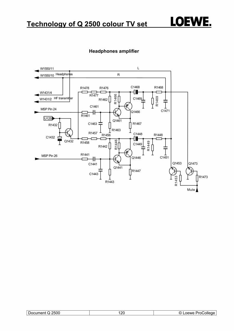
Technology of Q 2500 colour TV set
Document Q 2500 120 © Loewe ProCollege
U12S
R
L
C1451
R1448
R14
49C1449
C1448R1456R1457
R1458
Q1446
R14
46
Q1441R1447
R1443
R1442
C1441
R1441
C1471
R1468
R14
69
C1468R1476
R1477
R1478
Q1466
R1467Q1461
R14
66
R1462
R1463
C1461
R1461
Q1432C1432
R1432
R1473R
1453
Q1473Q1453
C1469
C1463
C1443
W1550/10
W1550/11Headphones
HF transmitterW1431/2
W1431/4
MSP Pin 24
MSP Pin 26
Mute
Headphones amplifier

Technology of Q 2500 colour TV set
Document Q 2500 121 © Loewe ProCollege
5.3 AC3 module (Dolby Digital)
5.3.1 Block diagram, AC3 module
5.3.2 AC 3 signal processing A Dolby Digital Module can also be incorpo-rated into the signal board variants Q 2500/H and Q 2500/M. If a signal board is fitted with the AC 3 module, the essential sound signal processing takes place on the AC 3 module. The AC 3 module supports: - Dolby Pro Logic - Dolby Digital 5.1 - Circle Surround - PCM Stereo
Dolby Digital 5.1 and Circle Surround can supply up to 6 sound channels. - 2 channels for Front left and right - 2 channels for Surround left and right - 1 Centre channel - 1 deep sound channel (LFE low fre-
quency effects) The Dolby Digital 5.1 Decoder is only active, when a correct AC 3 audio digital signal is supplied from a signal source.
LSLS
RSRS
LL
RR
CC
LFELFE
LCLC
RCRC
LSLS RSRS
SP-DIFSP-DIF
LL
RR
CC
LFELFE
CC
LL
RRLFELFE
RESETRESETRESETRESET LL
RR
CC
LFELFE
LCLC
RCRC
SP-DIF IN 1SP-DIF IN 1
SP-DIF IN 2SP-DIF IN 2
SP-DIF IN 3SP-DIF IN 3
I²C1I²C1
I²S2I²S2
SP-DIF INSP-DIF IN
3 X I²S3 X I²S
I²C1I²C1
I²C1I²C1
SOUND TABLESOUND TABLE
P16P16P17P17
P12P12P13P13
P10P10P11P11
P1P1P2P2
P7P7
P5P5P6P6
P3P3P4P4
P0P0
AUDIO OSZ.AUDIO OSZ.
PCF8
575
16 b
it I²C
Expa
nder
PCF8
575
16 b
it I²C
Expa
nder
CS 4226D/A-Converter
6 X 20 bit
CS 4226D/A-Converter
6 X 20 bit
CS 492505Multi Channel Digital Audio
Decoder
CS 492505Multi Channel Digital Audio
Decoder
NJM2234NJM2234
AT27LV020AROM
AT27LV020AROM
SSM2404SHEF 4053Speaker
ConfigurationMatrix
SSM2404SHEF 4053Speaker
ConfigurationMatrix
MC34063DC-DC
Converter
MC34063DC-DC
Converter
-12V12V
AC3 modul

Technology of Q 2500 colour TV set
Document Q 2500 122 © Loewe ProCollege
The Circle Surround Decoder operates with a normal stereo signal. From this stereo signal the decoder decodes the 6 sound channels. This function has the advantage that for the great majority of stereo transmitters a 5.1 sur-round signal can already be used. Dolby Pro Logic supports four sound chan-nels. 2 channels for front left and right 1 centre channel 1 mono surround channel Dolby Pro Logic also operates with a stereo signal, this must, however, also be coded with the Dolby Pro Logic standard. If this is not the case then no Center/Surround Signal is pro-duced. NF bandwidth of the sound channels Dolby
Pro Logic
Dolby Digital 5.1
Circle Surround
2 channels Front L/R
20Hz-20KHz
20Hz-20KHz
20Hz-20KHz
2 channels Surround
no 20Hz-20KHz
20Hz-20KHz
Mono Surround
100-7kHz
no no
Center 20Hz-7KHz
20Hz-20KHz
20Hz-20KHz
Deepsound- channel LFE
no 20Hz-100Hz
20Hz-100Hz
The AC 3 modules can receive digital audio signals via three paths. • I2S bus data supplied from MSP 341x on
the signal board. • SPDIF audio data from the two digital Au-
dio Cinch input sockets. • SPDIF audio data form the internal DVBi 2
Decoder (deliverable end 2002, not used in all device variants).
The AC 3 module cannot process any ana-logue sound signals directly. The analogue
sound signals from internal – e.g. Sat unit, tuner or DB module – as also from external – e.g. video recorder – sound signal sources, must first be converted into digital sound bus data (I2S bus). This task is implemented by the Multi Sound Processor MSP 341x, which is incorporated into the signal board. The digital I2S bus data is emitted by MSP I 2051 on pins 4/5 and 6 and are fed to the AC 3 module via pins 5/6/7 of contact connector W 2071. All analogue sound output signals to the AV sockets and the headphones amplifier are delivered by the MSP. The AC 3 module has no influence on these output signals. The AC 3 module does not deliver any I2S bus data back to the MSP. This also means that no sound signals are delivered to the AV sockets and the headphones amplifier, if sig-nals are supplied only via the SPDIF Cinch sockets. The SPDIF signals (SPDIF Sony Philips Digi-tal InterFace, level 0.7 Vss-1 Vss to 75 Ohm) are supplied by the Cinch sockets to the con-tact strip W 2091 pin 14 SPDIF in1 and pin 11 SPDIF in2. SPDIF data from DVBi 2 module is supplied to W 2091 pin 10. The SPDIF signals reach the AC 3 module on changeover switch I 18. This is controlled by the I2C bus expander I 11 via pin 2/4. The SPDIF signal selected for processing is output to pin 7 of I 18. The selected signal is also returned to the SPDIF Cinch outputs via pin 12 of Q 11 and W 301. I 2 converts the SPDIF signal – input pin 42 – of the I2S bus data – I 2 pins 1/43/44 - from MSP in the I2S bus data for the I 1 (DSP - Digital Sound Processor). I 1 processes this audio data according to the prescribed stan-dard. For this the respective software required is loaded from I 5 memory. The memory is organised into 8 blocks, each of 32 kByte. For Circle Surround, Doby Pro Logic and Dolby Digital a 32 kByte block respectively is re-quired. If, for example, Circle Surround is switched to Dolby Surround, the CCU controls Expander I 11 via the I2C bus in such a way that the address switching lines I 11 pin 9/10/11 of the memory block in I 5 for Dolby Surround can be selected. DSP I 1 receives an interrupt from CCU pin 77 via pin 14 of W 321.

Technology of Q 2500 colour TV set
Document Q 2500 123 © Loewe ProCollege
The interrupt causes I 2 to load new software from the memory. Due to the block pre-selection from the the I2C bus expander, the DSP now loads the software for Dolby Pro Logic. The DSP processes the I2S bus data accord-ing to the appropriate instructions. The over-whelming number of sound parameters to be set also occur in the DSP. The DSP feeds the digital sound bus data back to the converter I 2, where the digi-tal/analogue conversion takes place. The 6 sound output channels of I 2 reach W 301 via the operational amplifier and the loudspeaker matrix – consisting of I 6/9/14. - pin 1 LFE/SUB (deep sound channel) - pin 2 RS (Surround right) - pin 3 LS (Surround left) - pin 4 R (Front right) - pin 5 L (Front left) - pin 6 LC (Center left) - pin 7 RC (Center right) - pin 8 C (Center channel)
5.3.3 AC 3 IC functions CS 4925-01 (I 1) Multi Channel Digital Audio Decoder. - Processes according to the operating
mode, - Circle Surround, Dolby Pro Logic Dolby, Digital 5.1 - digital Sound-bus-data.
- Implements all sound settings, such as height and depth settings.
CS 4226 (I 2) DAC - Converts SPDIF signals into I2S bus data
for I 1 .
- Converts the I2S bus data processed by I 1 into analogue signals for the loud-speaker matrix.
6 Interface switching Interface switching is via Q 2500 on the signal board. Switching of the various on and off sig-nals is implemented essentially by six ICs; two TEA 6415, two CD 4053 for the video signals, a TEA 6422 and a TEA 6420 for the audio signal switching. Control is directly from I²C bus system 3 via SDA 6000. An exception is CD 4053 I 1631 and I 1771. I 1631 switches between the RGB lines of the AV3 socket and the RGB signals of the DVB decoder. I 1631 is controlled from a free switch output in MSP, which itself is activated by the CCU via the I2C bus. If the output on pin 78 of the MSP is switched to H level, then L level is felt on pins 9/10/11 of I 1631 via in-verter Q 1637. With L level on, its control input I1631 switches to AV3 operation, at H level the RGB signals from the DVB decoder are switched through to the signal processing. I 1771 is used for chroma signal switching if a Digital Link Plus SVHS video recorder is con-nected. During SVHS operation a chroma signal is expected from SVHS Digital Link Plus video recorders on pin 7 of the AV socket. For VHS video recorders it is pin 15. If the device control detects a SVHS Digital Link Plus VCR, the chroma signal is switched to pin 7 of the AV1 or AV2 socket on overplay and during a DVB recording. I 1771 is switched from two switch outputs on pin 115/116 I 2311. This in turn is controlled by the CCU. As the two TEA 6415 must be addressed dif-ferently for picture signal switching, pin 7 of I 1116 is earthed and I 1181 is at the operating voltage. The exact signal flow for the video and audio signals can be obtained from the appropriate flow diagrams.