Embed Size (px)
Citation preview
Techniques and Trade-offs in Low Power Wireless Transceivers
Alyosha Molnar Cornell University

Low Power Wireless
Driven by a need for data transfer to/from small, low-cost wireless nodes: IoT
Examples:
Wireless sensors (wearable, automation, etc.)
Medical implants
Identification/tracking: of livestock, inventory, etc.
2

What is “Low Power” Wireless?
Back-off performance to save significant power:
~1-10mW DC power when active.
Links can be symmetric or asymmetric
What can be traded off for power:
1. Range (Path loss)
2. Data rate
3. Spectral efficiency
4. Interference tolerance (Receiver)
5. Emission mask (Transmitter)
Low power implies low cost and/or small size
Otherwise just use a larger battery
TX RX PTX FRX
Path
Loss
3

What Limits Power in Circuits?
Analog gain: 𝑔𝑚 = 𝐼𝐷 𝑉𝑥 where 𝑉𝑇 < 𝑉𝑥 < 𝑉𝑠𝑎𝑡
𝑔𝑚 sets noise: 𝑣𝑛2 = 4𝑘𝑇𝛾 𝑔𝑚
Voltage gain (Av): Want high load Z (small CL)
𝐴𝑣 = 𝑔𝑚𝑟𝑜 or 𝐴𝑣 = 𝑔𝑚 𝜔𝐶𝐿 ∝ 𝜔𝑇 𝜔
Av independent of Pdc (!)
Self-biased inverter (2 × 𝑔𝑚)
CS with resonant load:
𝐴𝑣 = 𝑔𝑚 𝜔 ∙ 𝐿 ∙ 𝑄 C often explicit
Therefore, Av set by power, available inductor
Oscillators: just Av>1
Hard limit: 𝑃𝐷𝐶 > 𝑉𝐷𝐷𝑉𝑥 𝜔 ∙ 𝐿 ∙ 𝑄
Digital: 𝑃𝐷𝐶 = 𝐶𝑉𝐷𝐷2𝑓𝑐𝑙𝑘 Frequency dividers,
DSP
Vin
VDD
Vout
Inductor
sets Pdc
Vin
VDD
Vout
Ibias
gmn||gmp
CL
* Ibias
4

What Sets System Power?
Spectral efficiency (SE=bps/Hz), data rate
(DR), and path loss (PL), set link budget:
Data rate, path loss (range) trade off
TX: Output power PTX affects link budget
Total: PA plus overhead: 𝑃𝐷𝐶 = 𝑃𝑇𝑋 𝜂 + 𝑃𝑂𝐻𝑇𝑋
RX: Noise factor, FRX affects link budget
Low FRX takes power: 𝐹𝑅𝑋 > 1 + 𝛾 𝑉𝑥 (𝑅𝑆𝐼𝐿𝑁𝐴)
Higher source impedance helps
Power consumption 𝑃𝐷𝐶 = 𝑉𝐷𝐷𝐼𝐿𝑁𝐴 + 𝑃𝑂𝐻𝑅𝑋
Can trade RX and TX power for same link.
Need to minimize overhead power
Keep SE ~ 1bps/Hz
TX RX PTX FRX
Path
Loss
𝑆𝐸 ∙ 2𝑆𝐸 − 1 ∙ 𝐷𝑅 𝑃𝐿 < PTX 𝑘 ∙ 𝑇 ∙ 𝐹𝑅𝑋
0.0
50.0
100.0
150.0
200.0
250.0
300.0
0 200 400 600 800 1,000
PT
X, u
W
Pdc, uW
PO
HT
X
TX PDC vs Link
0.0
5.0
10.0
15.0
20.0
25.0
30.0
0 200 400 600 800 1,000
No
ise f
loo
r, F
Pdc, uW
PO
HR
X
RX PDC vs Link
5

TX Design
0/90
FSK
OOK
BPSK
PA: efficiency η~30%-50%
Key: match VDD and RL to PTX
Reasonable: 100µW-10mW
Overhead: Oscillator, dividers, LO buffers, phase splitters, mixers/modulators
Drive PA from Osc. tank
Simple modulation (OOK, FSK or BPSK): no RF mixers, modulators, phase splitters
Overhead is just Oscillator
𝑃𝑂𝐻𝑇𝑋 > 𝑉𝐷𝐷𝑉𝑥 𝜔 ∙ 𝐿 ∙ 𝑄
100µW-500µW reasonable
PTX=VDD2/2RL PTX=VDD2/8RL PTX=VDD2/8N2RL
Medium:
CS with LC Low:
inverter
Very Low:
stacked
6

Simple Receivers
Simplest idea: power detector
RF voltage gain, rectifier
Gain after 1st Amp is POH: can be very low.
Not very interference tolerant
• Assumes ASK (OOK) modulation
Related: super-regenerative
RF LNTA drives osc. “on the edge”
Oscillator converts Av~1 “”
More selective: Very high Q.
Still sensitive to interference (pulling)
Can be difficult to quench/control
Sets
noise
Overhead
Sets
noise
Overhead
Need V>26mV
here
7
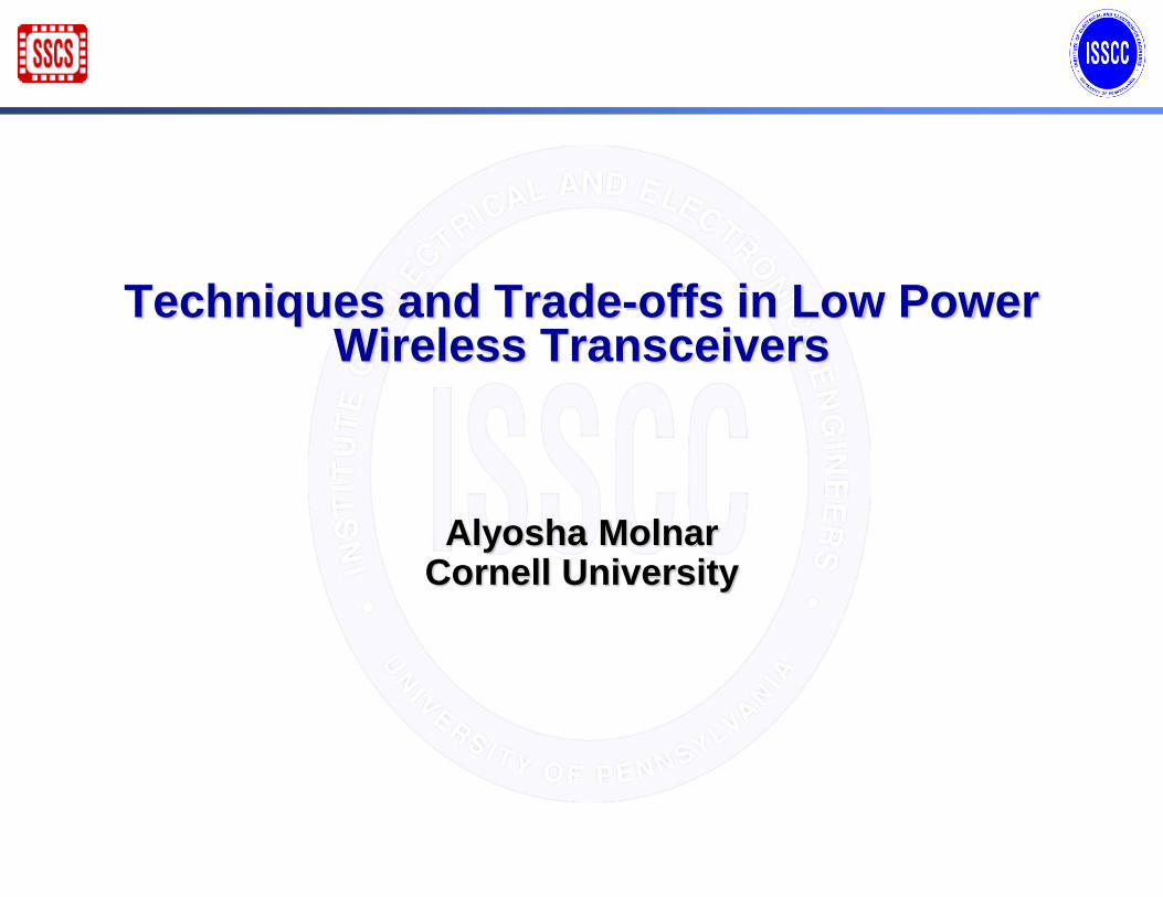
Low/Zero IF RX
Oscillator sets POH same as TX
Passive mixers no DC power
Osc. tank absorbs mixer gate Low IF not much more power than super regenerative.
Spend power in 1st amplifier for noise
Can be before mixer or after.
Additional analog processing at IF:
IF gain, filter, demod. ~free.
Selectivity better than LC tank
More modulations possible
Key trade off: image rejection (2x FRX)vs PDC (~2x POH)
Demod
passive
Demod
passive Small Overhead
Small Overhead
I
Q
0/90
8
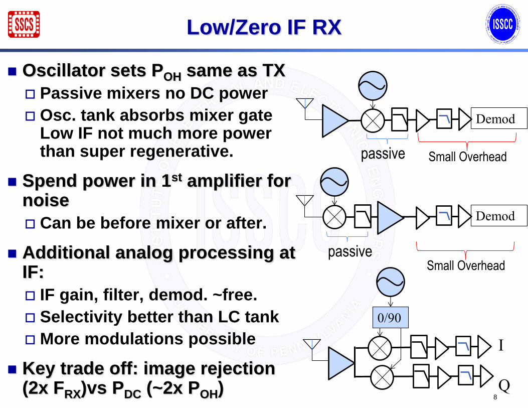
Optimizing VDD
VDD impacts circuit efficiency:
LNA efficiency
PA power level
Oscillator
Digital
VDD set by available supply:
Efficient battery: Li-cell >3V
Photovoltaic: ~400mV
Circuits should be designed for available VDD
How optimize?
Switched-cap buck/boost
Circuit stacking
Demod
passive
VLO
Vbatt
VDD
osc
VDD
LNA
SC reg
9

Accuracy/ Duty Cycle
Precision in FLO costs POH:
Cheaper to calibrate, hold than continuous PLL
Can increase BW to absorb error in FLO
Worse spectral efficiency, worse noise
Less proportional cost if data rate is higher
Duty cycle by 1/N : increases instantaneous DR by N
N x higher instantaneous LNA/PA Power (same avg).
But can duty cycle overhead too: POH/N
Costs of duty cycling:
Overhead for synch
Start-up overhead/settling
“0” “1”
Ideal FSK
“0” “1”
Adjusted for LO error
FLO
TX time
PDC
RX time PDC
settling
10

Exploiting Asymmetric Links
If one terminal (base station) has lots of power, save at other end:
Save Rx power by boosting PTXbase.
Other way harder: FRXbase>1 always, so PTXterm not too low.
Other asymmetries: LO gen: terminal locks to base
(saved POHTX)
Data rate: can benefit if DR downlink >> uplink
Duty cycling synch overhead taken by base
TX
RX
RX
TX
Base Term PTXbase
PTXterm
11
Conclusions
Reducing power in wireless circuits costs:
Data rate, range, spectral efficiency
Power Savings comes from:
Appropriate LNA, PA trade off
Architecture to minimize overhead
Optimize for available VDD
Reduced accuracy, optimal duty cycling
Circuit optimization
12


![Multiband Transceivers - [Chapter 4] Design Parameters of Wireless Radios](https://img.dokumen.tips/doc/110x75/55cebbd7bb61eb8c2f8b4620/multiband-transceivers-chapter-4-design-parameters-of-wireless-radios.jpg)