Embed Size (px)
Citation preview

Authors:
¬ Tioc Deac Daria ¬ Popoviciu Carmen ¬ Vicas Cristian ¬ Utiu Paul
Technical University of Cluj-Napoca Computer Science – Group 3023 2004

Amp Project – 2004 – UTCN – microprocessor
2
Table of Contents
I. Introduction I.1. Précis
I.2. Instruction set
II. The synthesis of the execution unit II.1. Declarations & functional description
II.2. The schematic & additional declarations
II.3. Implementation
II.4. Command variables
III. The synthesis of the command unit III.1. Instruction set
III.2. Declarations & functional description
III.3. The schematic & additional declarations
III.4. Implementation
IV. The implementation of the command unit
IV.1. Adjusting the micro-program
IV.2. The memory program
IV.3. The instruction decoder program
V. Appendix A - The Test Bench
Amp Project – 2004 – UTCN – microprocessor
3
I. Introduction
I.1. Précis
Applying the method of synthesizing numerical systems for implementing an 8-bit
microprocessor, defined by the totality of its instructions, has the purpose of illustrating the
following:
¬ Implementing an execution unit that includes a BUS and needs to use a TRI-STATE
BUFFER;
¬ Using a synchronized RAM ;
¬ Implementing a CASE microinstruction;
¬ Employing a sequencer available in the form of an integrated circuit for batch
processing;
¬ Implementing a vertical micro-program that will use several types of micro-instructions
and a subprogram.
I.2. Instruction set
The format and contents of the processor micro-instructions make up the instruction set of the
numerical system. Figure 1 shows the format of the instructions of the microprocessor.
According to this format, each of the instructions occupies one or two positions in the 8-bit
word memory. These fields are as follows:
¬ OPCODE (Operation Code);
¬ AM (Addressing Mode);
¬ JC (Jump Condition);
¬ An operand or an address m;
¬ Number n of the peripheral
OPCODE AM JC
m
7 4 3 2 1 0
OPCODE N
7 4 3 2 1 0
Figure 1
The instructions of the microprocessor are presented in Figure 2. They include 4 transfer
instructions denoted by the word LOAD, an arithmetic ADD instruction, 3 logic instructions -

Amp Project – 2004 – UTCN – microprocessor
4
AND, CPL, RRC, and two JUMP instructions. These instructions and their description are
shown in Figure 2 .
Instruction Description OPCODE
LOAD A, s A<-s 0000
LOAD d, A d<-A 0001
ADD A, s (C,A)<-A+s, Z<-Ùi not(A+s)i 0010
AND A, s A<-A Ù s, C<-0, Z<-Ùi not(A Ù s)i 0011
JUMP m PC<-m 0100
JUMP t, m PC<-not F*(PC+1) v F*m 0101
CPL A A<-not A 1000
RRC A A<-(C,A)/2, C<-A0 1001
LOAD A, IN A<-IN 1010
LOAD OUT, A OUT<-A 1011
Figure 2
The instructions in the table employ:
¬ An accumulator A;
¬ One source position s in the memory M;
¬ One destination position d in the memory M;
¬ One Carry flag C;
¬ One Zero flag Z;
¬ One Program Counter PC;
¬ One jump condition t;
¬ One state selector F;
¬ One Input Register In;
¬ One Output Register Out;
Figure 3 defines the source and destination positions in the memory according to the chosen
addressing mode. The four possible jump conditions are shown in Figure 4 .
Addressing mode Memory Description AM
Immediately s=#m s=m 00
Absolute s=s=m s=d=M(m) 01
Indirect s=d=(m) s=d=M(M(m)) 11
Figure 3
Condition Memory Description JC
Carry Set t=CS F=C 00
Carry Clear t=CC F=not C 01
Zero Set t=ZS F=Z 10

Amp Project – 2004 – UTCN – microprocessor
5
Zero Clear t=ZC F=not Z 11
Figure 4
II. The synthesis of the execution unit
II.1. Declarations & functional description
The execution unit of the microprocessor implements the instructions presented in Figure 2
using the registers:
A1x8 As an accumulator
C1x1 As a carry flag
Z1x1 As a zero flag
AR1x8 As an Address Register
IR1x8 As an Instruction Register for the operation code, the addressing mode and
the jump condition or the number of the peripheral for the current instruction
PC1x8 As an address counter for the next instruction address
IN1x8 As an Input Register
OUT1x8 As an Output Register
M256x8 As a memory for the given data and the micro-program
F1x1 As a state selector for the conditional jump instruction
The functioning of this microprocessor is described below, in Figure 5:
Figure 5

Amp Project – 2004 – UTCN – microprocessor
6
II.2. The schematic & additional declarations
The schematic of the execution unit of the microprocessor is depicted in Figure 6. This
schematic connects the registers and the resources defined previously in such a way as to
ensure all the types of information transfer described in Figure 5 .
Figure 6
ALU1x8 As an Arithmetic and Logical Unit
BUS1x8 As a unique data and address bus
II.3. Implementation
The implementation of the execution unit consists in choosing the registers and resources
capable of performing the operations described in the schematic. To make this easier we’ll
express the 12 distinct operations from the schematic taking into account the BUS and the
ALU:
1 BUS=PC, AR<-BUS, PC<-PC+1
2 BUS=M(AR), IR<-BUS
3 BUS=M(AR), AR<-BUS
4 BUS=M(AR), A<-ALU, ALU=BUS
5 BUS=A, M(AR)<-BUS
6 BUS=M(AR), (C,A)<-ALU, Z<-Ùi not ALU i, ALU=A+BUS
7 BUS=M(AR), A<-ALU, C<-0, Z <-Ùi not ALU i, ALU=A Ù BUS
8 BUS=M(AR), PC<-BUS
9 A<-ALU, ALU=not A
10 A<-(C,A)/2, C<-A0
11 BUS=IN(IR3:0), A<-ALU, ALU=BUS
12 BUS=A, OUT(IR3:0)<-BUS

Amp Project – 2004 – UTCN – microprocessor
7
We can now determine the number and the type of the operations performed by each of the
registers and resources in the execution unit. For example, the accumulator A loads the
output of the ALU, shifts right by one bit and executes the neutral operation. One register 2 x
(74194) is composed of two bidirectional shift registers on 4 bits (74194) that suit our purpose
perfectly. Figure 7 shows the interconnection of the chosen registers and resources such as
to fit the table above. In this schematic, the Zero flag (Z), the Address Register (AR), the
Instruction Register (IR) and the Output Register (OUT) are implemented using bidirectional
shifting registers (74194) as well.
Figure 7a

Amp Project – 2004 – UTCN – microprocessor
8
Figure 7b
The carry flag C corresponds to the sequential circuits (7408; 74194), the program counter PC
is implemented using two 4-bit binary counters (74163) and the memory M using two
synchronized sequential circuits (2101; 74100/2). The ALU 2 x (74181) doesn’t detect null
results, the logic product of the complement of its output variables ALU0 to ALU7, is performed
by two 4-bit comparators. The BUS needs to use 8 tri-state buffers (74244/2). The state
selector F is a 1:8 multiplexer that outputs the value of the carry or the zero flag or of their
complement according to the jump conditions in Figure 4.

Amp Project – 2004 – UTCN – microprocessor
9
We changed a little the implementation because of the bigger flexibility of VHDL. Next we will present the principal components that we built. The accumulator entity is: entity ACCUMULATOR is port ( CLK, S1, S0, SIN,reset: in std_logic; INPUT: in std_logic_vector ( 7 downto 0 ); SOUT: out std_logic; OUTPUT: out std_logic_vector ( 7 downto 0 )); end ACCUMULATOR; We have a synchronous circuit, with a reset signal active low. The s1, s0 functionality is described in table 8b/c. The ALU entity is a combinational logic circuit: entity proc_alu is port ( A:in std_logic_vector (7 downto 0); B:in std_logic_vector (7 downto 0); M_ALU,S3_ALU,S1_ALU,S0_ALU : in std_logic; res: out std_logic_vector (7 downto 0); carry, zero : out std_logic ); end proc_alu; Again, the control signals are described in table 8. We implemented it using an arithmetic part and a logic part: entity adder_8b is port ( A1, B1: in std_logic_vector ( 7 downto 0 ); CIN: in std_logic; S: out std_logic_vector ( 7 downto 0 ); COUT: out std_logic); end adder_8b; Here we have an full adder on 8 bits witc Carry in and Carry out. entity logic is port ( A2: in std_logic_vector ( 7 downto 0 ); B2: in std_logic_vector ( 7 downto 0 ); S3_ALU,S1_ALU,S0_ALU: in std_logiC; res_l: out std_logic_vector (7 downto 0)); end logic; We execute the logic operations AND and NOT as specified in the table 8, s3, s1, s0 signals. The two results, res1 and res2 are combined in the ALU arhitecture as shown below: res <= ( res1 and ( 7 downto 0 => nc ) ) or ( res2 and ( 7 downto 0 => M_ALU ) ); We also compute the ZERO and the CARRY flags: begin if res1 = "00000000" then z1 <= '1'; else z1 <= '0'; end if; if res2 = "00000000" then z2 <= '1'; else z2 <= '0';

Amp Project – 2004 – UTCN – microprocessor
10
end if; end process; zero <= ( z1 and nc ) or ( z2 and M_ALU); carry <= cc and nc;
ZERO and CARRY flags are synchronous, with an reset active low, FLAG is a multiplexer,
selecting the output according to Jump Condition, bit 1 and 0 from instruction, according to
table 4.
Program Counter is an synchronous circuit, with RESET signal active low.
entity PROGRAM_COUNTER is
port ( CLK, LD, P, RESET: in std_logic;
INPUT: in std_logic_vector ( 7 downto 0 );
OUTPUT: out std_logic_vector ( 7 downto 0 ));
end PROGRAM_COUNTER;
Tri State buffer is actually a multiplexer 4:1 on 8 bits , with the output connected to the BUS.
Selection is made according to A_BUS and B_BUS signals.
entity tri_state_buffer is
port ( input_signalA,
input_signalIN,
input_signalPC,
input_signalM: in std_logic_vector ( 7 downto 0 );
A,B,RESET : in std_logic;
output_signal: out std_logic_vector ( 7 downto 0 )
);
end tri_state_buffer;
Address Register, Instruction Register and OUT register are synchronous circuits that loads
the data from the input, according to LD signal, according to table 4.
RAM is implemented using TextIO routines. We load the memory content on RESET signal,
(active low) from memdata.txt file. It contains 256 binary strings, each string is on a line, and
each string contains 8 binary values, 0 or 1.
Execution unit contains all these components “wired” according to Figure 6 .
Amp Project – 2004 – UTCN – microprocessor
11
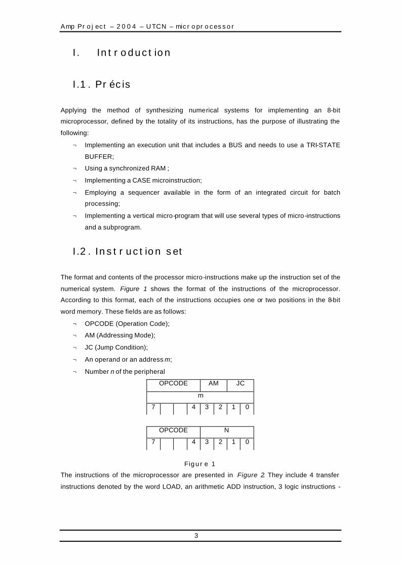
II.4. Command variables
Taking into account the registers and resources we have chosen for implementing the
execution unit, we must define values of the command variables for them to execute the
operations in the table and the NOP operation. This operation will allow the implementation of
a command unit whose micro -program contains several types of microinstructions. The values
that have to be attributed to the command variables are specified in the operations table of the
execution unit in Figure 8. They are taken from the respective operations tables of the
registers and resources we have chosen.
Operation Description
OP0 NOP
OP1 BUS=PC, AR<-BUS, PC<-PC+1
OP2 BUS=M(AR), IR<-BUS
OP3 BUS=M(AR), AR<-BUS
OP4 BUS=M(AR), A<-ALU, ALU=BUS
OP5 BUS=A, M(AR)<-BUS
OP6 BUS=M(AR), (C,A)<-ALU, Z<-Ùi not ALU i, ALU=A+BUS
OP7 BUS=M(AR), A<-ALU, C<-0, Z<-Ùi not ALU i, ALU=A Ù BUS
OP8 BUS=M(AR), PC<-BUS
OP9 A<-ALU, ALU<=not A
OP10 A<-(C,A)/2, C<-A0
OP11 BUS=IN(IR3:0), A<-ALU, ALU=BUS
OP12 BUS=A, OUT(IR3:0)<-BUS
Figure 8a Ý Figure 8b ß
Operation S1OUT S0OUT S1A S0A AC S1C S0C S1Z S0Z S1AR S0AR S1IR S0IR
OP0 0 0 0 0 Æ 0 0 0 0 0 0 0 0
OP1 0 0 0 0 Æ 0 0 0 0 1 1 0 0
OP2 0 0 0 0 Æ 0 0 0 0 0 0 1 1
OP3 0 0 0 0 Æ 0 0 0 0 1 1 0 0
OP4 0 0 1 1 Æ 0 0 0 0 0 0 0 0
OP5 0 0 0 0 Æ 0 0 0 0 0 0 0 0
OP6 0 0 1 1 1 1 1 1 1 0 0 0 0
OP7 0 0 1 1 0 1 1 1 1 0 0 0 0
OP8 0 0 0 0 Æ 0 0 0 0 0 0 0 0
OP9 0 0 1 1 Æ 0 0 0 0 0 0 0 0
OP10 0 0 0 1 Æ 0 1 0 0 0 0 0 0
OP11 0 0 1 1 Æ 0 0 0 0 0 0 0 0
OP12 1 1 0 0 Æ 0 0 0 0 0 0 0 0

Amp Project – 2004 – UTCN – microprocessor
12
Operation CLRPC LDPC PPC WM MALU S3ALU S2ALU S1ALU S0ALU GIN GA GPC GM
OP0 1 1 0 0 Æ Æ Æ Æ Æ Æ 1 1 1
1 Æ 1 1
1 1 Æ 1
1 1 1 Æ
OP1 1 1 1 0 Æ Æ Æ Æ Æ 1 1 0 1
OP2 1 1 0 0 Æ Æ Æ Æ Æ 1 1 1 0
OP3 1 1 0 0 Æ Æ Æ Æ Æ 1 1 1 0
OP4 1 1 0 0 1 1 0 1 0 1 1 1 0
OP5 1 1 0 1 Æ Æ Æ Æ Æ 1 0 1 1
OP6 1 1 0 0 0 1 0 0 1 1 1 1 0
OP7 1 1 0 0 1 1 0 1 1 1 1 1 0
OP8 1 0 Æ 0 Æ Æ Æ Æ Æ 1 1 1 0
OP9 1 1 0 0 1 0 0 0 0 Æ 1 1 1
1 Æ 1 1
1 1 Æ 1
1 1 1 Æ
OP10 1 1 0 0 Æ Æ Æ Æ Æ Æ 1 1 1
1 Æ 1 1
1 1 Æ 1
1 1 1 Æ
OP11 1 1 0 0 1 1 0 1 0 0 1 1 1
OP12 1 1 0 0 Æ Æ Æ Æ Æ 1 0 1 1
Figure 8c Ý Figure 8d ß
Operation BBUS ABUS
OP0 Æ Æ
OP1 0 1
OP2 0 0
OP3 0 0
OP4 0 0
OP5 1 0
OP6 0 0
OP7 0 0
OP8 0 0
OP9 Æ Æ
OP10 Æ Æ
OP11 1 1

Amp Project – 2004 – UTCN – microprocessor
13
OP12 1 0
To reduce the length of the micro-program, it is enough to place a decoder at the output of the
command unit. This decoder also ensures the coding of the G (enable) command variables of
the tri-state buffers connected to the BUS using only two auxiliary variables ABUS and BBUS as
shown in Figure 8d .
The implementation of the command unit will simplify if we allow all the command variables to
be 0 for the null operation. The command unit has to generate a set of minimal distinct
variables that will depend on the inverse of the variables LDPC (active low) and CLRPC (active
low) from the execution unit. Two of the state variables can be reduced to constants:
13 S2ALU =0
14 CLRPC=0
The partial graph in which only compatible variables appear determines a set of 16 distinct
variables.
15 C0=ABUS
16 C1=BBUS
17 C2=S1ALU
18 C3=WM
19 C4=LDPC
20 C5=S0IR=S1IR
21 C6= S0AR=S1AR
22 C7=S0C
23 C8=S1A
24 C9=S0OUT=S1OUT
25 C10=S0ALU=S0Z=S1Z=S1C
26 C11=S3ALU
27 C12=MALU
28 C13=PPC
29 C14=AC
30 C15=S0A
By giving particular values to some of the “don’t care”s in Figure 8, the last 6 variables of the
ensemble will be computed from the first 10 by simple logic operations:
31 C10= C7* C8
32 C11= C2+ C10
33 C12= C0+ C2
34 C13= C0* C6
35 not C2

Amp Project – 2004 – UTCN – microprocessor
14
36 C15= C7+ C8
The number of the command variables reduces to 10. Figure 10 shows the hexadecimal
values of these variables if all the undefined Æ values are chosen to be zero.
Operation C9:0
OP0 000
OP1 041
OP2 020
OP3 040
OP4 104
OP5 00A
OP6 180
OP7 184
OP8 010
OP9 101
OP10 080
OP11 107
OP12 202
Figure 10
Operation Description SF CF BF AF IR1 IR0
SELECT C F=C 0 0 0 0 0 0
SELECT not C F=not C 0 0 0 1 0 1
SELECT Z F=Z 0 0 1 0 1 0
SELECT not Z F=not Z 0 0 1 1 1 1
Figure 11
The operations performed by the state selector F don’t feature in the schematic of the
microprocessor. They are deduced from the jump conditions defined in the microinstructions
table and lead us to the table in Figure 11. As shown below, the selection of one or another
condition depends on the state of JC field which IR stores in its bits IR0 and IR1. So the
command variables of the selector will satisfy the following relations:
37 AF=IR0
38 BF=IR1
39 CF=0
40 SF=0

Amp Project – 2004 – UTCN – microprocessor
15
III. The synthesis of the command unit
III.1. Instruction set
The microinstructions table corresponds to the microinstructions in the command unit. It helps
to define the format and the fields of the microinstructions while specifying their relation with
the diamonds and rectangles in the state diagram. The table in Figure 12 associates a
multiple or binary test microinstruction to each diamond and a command, call, or return
instruction to each rectangle.
Figure 12
Applied to the state diagram of the microprocessor, this table leads us to the micro-program in
Figure 13. The GOTO FETCH instructions of the program correspond to the cycles in the
state diagram that bring the numerical system back to the initial operation. These are binary
test microinstructions that work on a null constant K.
FETCH: DO OP1
DO OP2
EXECUTE: CASE IR7:4 OF 0: GOTO LOAD A, s
1: GOTO LOAD d, A

Amp Project – 2004 – UTCN – microprocessor
16
2: GOTO ADD A, s
3: GOTO AND A, s
4: GOTO JUMP m
5: GOTO JUMP t, m
8: GOTO CPL, A
9: GOTO RRC A
A: GOTO LOAD A, $n
B: GOTO LOAD $n, A
LOAD A, s: CALL AM
DO OP4
GOTO FETCH
LOAD d, A: CALL AM
DO OP3
GOTO FETCH
ADD A, s: CALL AM
DO OP6
GOTO FETCH
AND A, s: CALL AM
DO OP7
GOTO FETCH
JUMP m: CALL AM
DO OP8
GOTO FETCH
JUMP t, m: CALL AM
IF F=0 THEN GOTO FETCH
DO OP8
GOTO FETCH
CPL A: DO OP9
GOTO FETCH
RRC A: DO OP10
GOTO FETCH
LOAD A, $n: DO OP11
GOTO FETCH
LOAD $n, A: DO OP12
GOTO FETCH
AM: DO OP1
IF IR2=0 THEN GOTO RETURN
DO OP3
IF IR3=0 THEN GOTO RETURN
DO OP3

Amp Project – 2004 – UTCN – microprocessor
17
RETURN: RET
Figure 13
The size of the micro-program, the number of binary test variables and of command variables
in the execution unit determine the format and the fields of the 5 microinstructions in Figure
14:
¬ The binary test microinstruction is defined by: 2 code bits MC2, MC1=00, a TEST field
for the selection of the test variable in the diamond and an ADR field that gives the
address ADR0 of the next instruction for the value 0 of the test variable;
¬ The multiple microinstruction is defined by 2 code bits MC2, MC1=01;
¬ The command microinstruction is defined by 2 code bits MC2, MC1=10 and an OP
field which gives the state of the command variables in the execution unit;
¬ The call microinstruction of the subprogram is defined by 3 code bits MC2:0=110 and
an ADR field which gives the address of the first microinstruction in the subprogram;
¬ The return microinstruction of the subprogram is defined by 3 code bits MC2:0=111.
0 0 TEST Æ ADR
11 10 9 8 7 6 5 0
0 1 Æ
11 10 9 0
1 0 OP
11 10 9 0
1 1 0 Æ ADR
11 9 8 6 5 0
1 1 1 Æ
11 9 8 0
Figure 14

Amp Project – 2004 – UTCN – microprocessor
18
III.2. Declarations & functional description
In order to execute the 5 microinstructions in Figure 14, the command unit of the
microprocessor needs to use the following registers:
AR1x6 As an Address Memory Register
S1x6 As a Stack
M36x12 As the Memory
T1x1 As a test multiplexer
ID10x6 As an Instruction Decoder
C1x10 To cancel the command variables at the output
The state diagram in Figure 15 describes the functioning of the command unit for each of the
instructions, according to their MC code and for the initialization that takes place when I is 1:
Figure 15
III.3. The schematic & additional declarations
Through the elements declared above, the command unit schematic from Figure 16, includes
two supplementary resources:
INC1x6 To increment with a unit the address register
AM1x6 As an Address Multiplexer to select the address
from the memory or to decode the instruction
The input variables of the command unit come from the instruction register and the state
selector of the execution unit. The constant K=0 is used by the supplementary binary test
microinstructions GOTO FETCH:

Amp Project – 2004 – UTCN – microprocessor
19
Figure16
III.4. Implementation
The table in Figure 17a describes the operations in the command unit state diagram
according to the INC and AM. We have to choose a set of registers and resources capable to
perform these operations. So we use two 4-bit registers (74482) for AR, S and INC, also two
4-bit multiplexers (74157) with 2 inputs and 3 4-bit AND circuits (7408) for AM and the output
variables of C. The instruction decoder and memory M are implemented using 2 memories
EPROM of 2048x8 bits (2516).

Amp Project – 2004 – UTCN – microprocessor
20
Operation Description
OP1 AR<-INC, C=0, INC=AR+1
OP2 AR<-AM, C=0, AM=M(AR)ADR
OP3 AR<-AM, C=0, AM=ID(IR7:4)
OP4 AR<-INC, C=M(AR)OP, INC=AR+1
OP5 AR<-AM, S<-INC, C=0, INC=AR+1, AM=M(AR)ADR
OP6 AR<-S, S<-Æ, C=0
OP7 AR:=0, C=Æ
Figure 17a
CLRAR S6AR S5AR S4S S3S S2INC S1INC AC GAM SAM I MC2 MC1 MC0 T
1 1 0 0 0 0 1 0 Æ Æ 0 0 0 Æ 1
1 0 0 0 0 Æ Æ 0 0 0 0 0 0 Æ 0
1 0 0 0 0 Æ Æ 0 0 1 0 0 1 Æ Æ
1 1 0 0 0 0 1 1 Æ Æ 0 1 0 Æ Æ
1 0 0 1 Æ 0 1 0 0 0 0 1 1 0 Æ
1 0 1 Æ Æ Æ Æ 0 Æ Æ 0 1 1 1 Æ
0 Æ Æ Æ Æ Æ Æ Æ Æ Æ 1 Æ Æ Æ Æ
Figure 17b
Taking into account the chosen registers and resources, Figure 17b defines the state of the
variables of the command unit. The corresponding values for the initializing variable I, the
code bits MC and the test variable T lead us to the following relations:
37 SAM =not MC2 * MC1
38 GAM =0
39 AC=MC2 * not MC1
40 S1INC=1
41 S2INC=0
42 S3S=0
43 S4S=MC2 * MC1
44 S5AR=MC2 * MC1 * MC0
45 S6AR=MC2 * not MC1 + not MC0 * T
46 CLRAR=I
The test multiplexer T selects the variables F, IR2, IR3 or the constant K=0 . These operations
appear in the table in Figure 18 which depicts the state of the command variables of the 1:8
multiplexer used to perform them:

Amp Project – 2004 – UTCN – microprocessor
21
Operation Description ST CT BT AT TEST
SELECT F T=F 0 0 0 0 0 0
SELECT IR2 T=IR2 0 0 0 1 0 1
SELECT IR3 T=IR3 0 0 1 0 1 0
SELECT K=0 T=O 0 0 1 1 1 1
Figure 18
When implementing Figure 19 we interconnect the information variables of the registers to
those of the resources according to the schematic of the command unit, using some logical
gates. The decoder of the command variables of the execution unit presented in Figure 20, is
implemented according to the relations (15) to (36). The decoder uses a demultiplexer 1:4
(74139/2) to obtain the 0 to 4 encoding needed by the tri-state buffer. The 1:16 demultiplexers
(74154) allow 16 input and 16 output registers.
Figure 19

Amp Project – 2004 – UTCN – microprocessor
22
Figure 20
Using the flexibility of VHDL we built Address Register, the stack and INC in one circuit
controlled by the corresponding control signals.
entity AR is
port (
AM_IN: in std_logic_vector ( 5 downto 0 );
CLR_AR, S6, S5,s4,clk: in std_logic;
OUT_AR: out std_logic_vector ( 5 downto 0 ));
end AR;
The control signals are obtained using a combinational logic according to table 5.17 and
implemented in the Command Unit architecture. The ROM is a simple memory; it is initialized
on RESET signal (active low) with the values found in table 22.
In the same way, the Instruction Decoder is actually a kind of memory, initialized on RESET
signal with the values found in table 23.

Amp Project – 2004 – UTCN – microprocessor
23
IV. The implementation of the command unit
IV.1. Adjusting the micro-program
Adjusting the original program in Figure 13 is limited to counting the microinstructions in
hexadecimal staring from 0 and replacing the GOTO FETCH instructions with binary tests
operated on the constant K=0. The final program in Figure 21 only contains the
microinstructions in the table of the command unit and replaces the labels with hexadecimal
addresses.
00 DO OP1
01 DO OP2
02 CASE IR7:4 OF 0: GOTO 03
1: GOTO 06
2: GOTO 09
3: GOTO 0C
4: GOTO 0F
5: GOTO 12
8: GOTO 16
9: GOTO 18
A: GOTO 1A
B: GOTO 1C
03 CALL 1E
04 DO OP4
05 IF K=0 THEN GOTO 00
06 CALL 1E
07 DO OP5
08 IF K=0 THEN GOTO 00
09 CALL 1E
0A DO OP6
0B IF K=0 THEN GOTO 00
0C CALL 1E
0D DO OP7
0E IF K=0 THEN GOTO 00
0F CALL 1E
10 DO OP8
11 IF K=0 THEN GOTO 00
12 CALL 1E
13 IF F0 THEN GOTO 00

Amp Project – 2004 – UTCN – microprocessor
24
14 DO OP8
15 IF K=0 THEN GOTO 00
16 DO OP9
17 IF K=0 THEN GOTO 00
18 DO OP10
19 IF K=0 THEN GOTO 00
1A DO OP11
1B IF K=0 THEN GOTO 00
1C DO OP12
1D IF K=0 THEN GOTO 00
1E DO OP1
1F IF IR2=0 THEN GOTO 23
20 DO OP3
21 IF IR3=0 THEN GOTO 23
22 DO OP3
23 RET
Figure 21
IV.2. The memory program
Figure 22 shows the hexadecimal program of the memory M in the command unit when all the
unspecified fields of the microinstructions are chosen equal to 0. The implementation of this
program is based on the final program, taking into account the format of the instructions in
Figure 14, the encoding of the test variables in Figure 18 and the encoding of the command
variables in Figure 10.
ADR M(ADR) ADR M(ADR)
00 841 12 C1E
01 820 13 000
02 400 14 810
03 C1E 15 300
04 904 16 901
05 300 17 300
06 C1E 18 880
07 80A 19 300
08 300 1A 907
09 C1E 1B 300
0A 980 1C A02

Amp Project – 2004 – UTCN – microprocessor
25
0B 300 1D 300
0C C1E 1E 841
0D 984 1F 123
0E 300 20 840
0F C1E 21 223
10 810 22 840
11 300 23 E00
Figure 22
IV.3. The instruction decoder program
We have in Figure 23 the hexadecimal program of the instruction decoder ID, i.e. the
information that will be written in the EPROM used to implement the decoder. This program
can be deduced from the multiple test microinstruction of the final program.
ADR ID(ADR)
0 03
1 06
2 09
3 0C
4 0F
5 12
8 16
9 18
A 1A
B 1C
Figure 23

Amp Project – 2004 – UTCN – microprocessor
26
Appendix A - The Test Bench
We use a clock generator, the same used in the laboratory. We start with RESET on 0 (active
low). After a 1/2 clock period (defined in constant TIMECLK) we put RESET on 1 and so the
microcontroller starts to work.
There are 2 processes, one generates clock, and working until the END_SIM shared variable
becomes true.
The second process controls the input, the RESET signal is lowered we wait a while
(timeclk/2), the RESET is put to ‘1’ and the process halts.
Copyright © 2004. All rights reserved. Daria, Carmen, Visoft, SoftComm .