Embed Size (px)
Citation preview

Infineon Technologies Bipolar GmbH & Co. KG …for energy efficiency!
Ask Infineon. Get connected with the answers.Where you need it. When you need it.
Infineon offers its toll-free 0800/4001 service hotline as one central number, available 24/7 in English, Mandarin and German.
Our global connection service goes way beyond standard switchboard services by offering qualified support on the phone. Call us!
n Germany ..................... 0800 951 951 951 (German/English)
n China, mainland ......... 4001 200 951 (Mandarin/English)
n India ........................... 000 800 4402 951 (English)
n USA ............................ 1-866 951 9519 (English/German)
n Other countries ........... 00* 800 951 951 951 (English/German)
n Direct access .............. +49 89 234-0 (interconnection fee, German/English)
* Please note: Some countries may require you to dial a code other than “00” to access this international number, please visit www.infineon.com/service for your country!
Where to BuyInfineon Distribution Partners and Sales Offices
Please use our location finder to get in contact with your nearestInfineon distributor or sales office.
www.infineon.com/WhereToBuy www.ifbip-shop.com
Technical InformationBipolar Semiconductors
www.ifbip.com · www.ifbip-shop.com
AN2012-01
Published by Infineon Technologies Bipolar GmbH & Co. KGMax-Planck-Str. 559581 WarsteinTel. +49 (0) 2902 98 99-0Fax +49 (0) 2902 98 99-2482
© 2012 Infineon Technologies Bipolar GmbH & Co. KG. All Rights Reserved.
Visit us:www.ifbip.com · www.ifbip-shop.com
Order Number: B157-H9716-X-X-7600Date: 04 / 2012
AttentIon pleAse!The information given in this document shall in no event be regarded as a guarantee of conditions or characteristics (“Beschaffenheitsgarantie”). With respect to any examples or hints given herein, any typical values stated herein and/or any information regarding the application of the device, Infineon Technologies hereby disclaims any and all warran-ties and liabilities of any kind, including without limita- tion warranties of non-infringement of intellectual property rights of any third party.
InformAtIonFor further information on technology, delivery terms and conditions and prices please contact your nearest Infineon Technologies Office (www.infineon.com).
WArnInGsDue to technical requirements components may contain dangerous substances. For information on the types in question please contact your nearest Infineon Technologies Office. Infineon Technologies Components may only be used in life-support devices or systems with the express written approval of Infineon Technologies, if a failure of such components can reasonably be expected to cause the failure of that life-support device or system, or to affect the safety or effectiveness of that device or system. Life support devices or systems are intended to be implanted in the human body, or to support and/or maintain and sustain and/or protect human life. If they fail, it is reason-able to assume that the health of the user or other persons may be endangered.

Products and Innovations
600A/9.5 kV Thyristor Technologyfor Soft Starter and Power-Supplies
The goal of highest reliability and efficiency in a core technology is always a moving target; therefore we understand that continuous improvement is essential. On this basis we have established comprehensive standards with our technologies and our products, in the power classes ranging from around 10kW to over 30MW per component. These include for example:
■ PowerBLOCK modules in press-pack technology with currents up to 1100 Ampere■ Diodes and thyristors with a silicon diameter up to six inches and blocking voltages
up to 9500 Volts■ Light-triggered thyristors with integrated protection functions ■ Freewheeling diodes for the highest requirements in fast switching applications
such as with IGBTs or IGCTs
The 9.5 kV thyristor disc is developed and designed for the special requirements in medium voltage soft starter as well as for medium voltage power supply applications. For these kinds of applications it is necessary to use several thyristors in series con-nection. They are optimized to achieve an excellent voltage sharing under all operating conditions.
The device is designed for a high surge current capability. To ensure a narrow spread of dynamic parameters which enables best cost designs with less devices in series high technology production processes are used for this type.
Of course the thyristor is suitable for general purpose line voltage rectifier applications, e.g. for power supplies or standard electrical drives.

1
1. Introduction 61.1 Diode 61.2 Thyristor 7
2. Type and polarity designation 92.1 Designation of the terminals 92.2 Constructions 9
2.2.1 General 92.2.2 Disc cells 92.2.3 PowerBLOCK-Module 92.2.4 Stud type and flat case constructions 10
3. Electrical properties 113.1 Forward direction 11
3.1.1 Forward off-state current iD 123.1.2 Forward off-state voltage vD 12
3.1.2.1 Repetitive peak forward off-state voltage VDRM 123.1.2.2 Non-repetitive peak forward off-state voltage VDSM 133.1.2.3 Forward direct off-state voltage VD (DC) 13
3.1.3 Forward breakover voltage V(BO) 133.1.4 Open gate forward breakover voltage V(BO)0 133.1.5 Holding current IH 133.1.6 Latching current IL 133.1.7 On-state current iT, ITAV, ITRMS iF, IFAV, IFRMS 133.1.8 On-state voltage vT, vF 143.1.9 On-state characteristic 143.1.10 Equivalent line approximation with VT(TO), VF(TO) and rT 143.1.11 Maximum average on-state current ITAVM, IFAVM 153.1.12 Maximum RMS on-state current ITRMSM, IFRMSM 153.1.13 Overload on-state current IT(OV), IF(OV) 153.1.14 Maximum overload on-state current IT(OV)M, IF(OV)M 153.1.15 Surge on-state current ITSM, IFSM 173.1.16 Maximum rated value ∫i²dt 17
3.2 Reverse direction 183.2.1 Reverse current iR 183.2.2 Reverse voltage vR 18
3.2.2.1 Repetitive peak reverse voltage VRRM 183.2.2.2 Non-repetitive peak reverse voltage VRSM 183.2.2.3 Direct reverse voltage VR(DC) 18
3.3 Control properties of thyristors 193.3.1 Positive gate control 19
3.3.1.1 Gate current iG 193.3.1.2 Gate voltage VG 193.3.1.3 Gate trigger current IGT 19
Contents

2
3.3.1.4 Gate trigger voltage VGT 193.3.1.5 Gate non-trigger current IGD 193.3.1.6 Gate non-trigger voltage VGD 193.3.1.7 Control characteristic 203.3.1.8 Control circuit 203.3.1.9 Minimum duration of the trigger pulse tgmin 233.3.1.10 Maximum permissible peak trigger current 23
3.4 Carrier storage effect and switching characteristics 243.4.1 Turn-on 24
3.4.1.1 Diode 243.4.1.1.1 Peak value of the forward recovery voltage VFRM 253.4.1.1.2 On-state recovery time tfr 25
3.4.1.2 Thyristor 253.4.1.2.1 Gate controlled delay time tgd 263.4.1.2.2 Critical rate of rise of the on-state current (di/dt)cr 263.4.1.2.3 Repetitive turn-on current IT(RC)M 273.4.1.2.4 Critical rate of rise of off-state voltage (dv/dt)cr 27
3.4.2 Turn-off 273.4.2.1 Recovery charge Qr 273.4.2.2 Peak reverse recovery current IRM 293.4.2.3 Reverse recovery time trr 303.4.2.4 Turn-off time tq 30
3.5 Power dissipation (losses) 333.5.1 Total power dissipation Ptot 333.5.2 Off-state losses PD, PR 333.5.3 On-state losses PT, PF 333.5.4 Switching losses PTT, PFT+PRQ 34
3.5.4.1 Turn-on losses PTT, PFT 343.5.4.2 Turn-off losses PRQ 35
3.5.5 Gate dissipation PG 353.6 Insulation test voltage VISOL 35
4. Thermal properties 364.1 Temperatures 36
4.1.1 Junction temperature Tvj, Tvj max 364.1.2 Case temperature TC 364.1.3 Heatsink temperature TH 374.1.4 Cooling medium temperature TA 374.1.5 Junction operating temperature range Tcop 374.1.6 Storage temperature range Tstg 37
4.2 Thermal resistances 374.2.1 Internal thermal resistance RthJC 374.2.2 Thermal transfer resistance RthCH 374.2.3 Heatsink thermal resistance RthCA 384.2.4 Total thermal resistance RthJA 384.2.5 Transient internal thermal resistance ZthJC 384.2.6 Transient heatsink thermal resistance ZthCA 384.2.7 Total transient thermal resistance ZthJA 39

3
4.3 Cooling 394.3.1 Natural air cooling 394.3.2 Forced air cooling 394.3.3 Water cooling 394.3.4 Oil cooling 39
5. 5. Mechanical properties 405.1 Tightening torque 405.2 Clamping force 405.3 Creepage distance 405.4 Humidity classification 405.5 Vibration 405.6 UL-registration 40
6. Notes for applications 416.1 Case non-rupture current 416.2 Thermal load cycling 416.3 Parallel connection 426.4 Series connection 446.5 Pulsed Power 46
6.5.1 Applications with DC 466.5.2 Current rise time at turn-on 466.5.3 Zero crossing of current and voltage during turn-on 476.5.4 Turn-off with a high di/dt versus a negative voltage 47
7. Protection 497.1 Overvoltage protection 49
7.1.1 Individual snubbering (RC-snubber) 497.1.2 Input snubbering for AC-controllers 527.1.3 Supply snubbers for line commutated converters 537.1.4 Additional options for protection versus energy intensive overvoltages 55
7.2 Overcurrent protection 567.2.1 Short-term protection with superfast semiconductor fuses 56
7.2.1.1 Selection of fuses 567.2.2 Further protection concepts: short-term protection of high power semiconductors 59
7.2.2.1 High speed DC-circuit breakers 597.2.2.2 Crowbar (electronic short circuit) 597.2.2.3 Line side circuit breaker 597.2.2.4 Blocking of trigger pulses 59
7.2.3 Long-term protection 597.2.4 Fully rated protection 59
7.3 Dynamic current limiting with inductors in the load circuit 607.4 Reduction of interference pulses in the gate circuit 61

4
8. Mounting 628.1 Disc cases 62
8.1.1 Mounting of disc cells 628.1.2 Positioning the heatsinks 668.1.3 Connection of busbars 668.1.4 Connection of the control leads 67
8.2 Stud cases 678.2.1 Mounting stud cases 678.2.2 Positioning the heatsinks 678.2.3 Connection of busbars 688.2.4 Connection of the control leads 68
8.3 Flat base cases 688.3.1 Mounting flat base devices 688.3.2 Positioning the heatsinks 698.3.3 Connection of busbars 698.3.4 Connection of the control leads 69
8.4 PowerBLOCK-Modules 698.4.1 Mounting PowerBLOCK-modules 698.4.2 Positioning the heatsinks 698.4.3 Connection of busbars 708.4.4 Connection of the control leads 70
9. Maintenance 7010. Storage 7011. Type designation 7112. Circuit topologies 72A1. Abbreviations 74A2. List of Figures 76A3. List of tables 78A4. Conditions of use 79

5
PrefacePower semiconductors are the central components in converters technology. Due to constant advancement these components find further use in ever new and more complex applications.
Based on the suggestions and questions we have been approached with we compiled this Technical Information (TI) as a reference document.
This Technical Information describes all essential technical terms for bipolar power semiconductors (diodes and thyristors) and thus provides assistance in working and designing as well as a reference document for the development and projection of inverter circuitry with bipolar components.It is aimed at the relevant specialists in industry, research, development and training.
General information regarding converters, their circuits and specialties can be found in the pertinent literature.
At this point we refer to the appropriate standards which always need to be regarded in their latest version.
The current technical data of Infineon power semiconductors can be down-loaded from www.Infineon.com.
This Technical Information is meant to assist in better understanding the terms and the application of data sheet specifications of bipolar power semiconductors.Definitions and abbreviations used are mainly in accordance with DIN / IEC / EN.Please note that no guaranty can be given that circuits, appliances and processes described here are free of patent rights.

6
1. IntroductionThis TI is to give detailed definitions to specifications used in the data sheets. Further, the user is to be assisted to transfer the data sheet specifications correctly in his application. The following information is generally valid for all Infineon pressure contact components (disc cells and PowerBLOCK-Modules). Exceptions are individually marked. Information given here is valid in accordance with the currently valid norms and standards.
1.1 DiodeA diode is a component with one P and one N conducting semiconductor zone.The PN-junction is responsible for the elementary features of this semiconductor (see Figure 1).
Figure 1: Schematic construction of a diode
Figure 2 Characteristics of a diode
The characteristic of a diode is depicted in Figure 2. It consists of two sections: the blocking characteristic and on-state characteristic.
Technischer Erläuterungen - Bilder
K
A
PN
Kathode KCathode K
-
+ Anode A
Diode
K
A
PN
Kathode KCathode K
-
+ Anode A
Diode
Abb./Fig.1 Schematischer Aufbau einer Diode
Technischer Erläuterungen - Bilder
vF
iFDurchlaßkennlinieHigh conduction characteristic
DurchlassrichtungForward direction
SperrrichtungReverse Direction
vR
Rückwärts-SperrkennlinieReverse blocking characteristic
iR
Abb./Fig.2 Kennlinien einer Diode

7
When a voltage up to several kV is applied in reverse direction, reverse currents in the range of mA will flow via the main terminals anode and cathode. When a voltage is applied in forward direction, currents up to several kA will flow via the main terminals anode and cathode.
1.2 ThyristorA thyristor is a component with a total of four alternating P and N conducting semiconductor zones. These will thus form three PN-junctions (see Figure 3).
Figure 3: Schematic construction of a thyristor
Figure 4 Characteristics of a thyristor
The characteristics of a conventional (reverse blocking) thyristor are depicted in Figure 4. They consist of three sections: The blocking and the on-state characteristic in forward direction and the blocking characteristic in reverse direction.
As can be seen from the characteristics, the thyristor is initially blocked in forward and reverse directions. Generally the blocking capability is approximately the same in both directions. When voltages up to several kV are applied in forward or reverse direction, only small blocking currents will flow via the main terminals anode and cathode. An additional control current IG between control terminal (gate) and cathode
Technischer Erläuterungen - Bilder
K
A
G
PNPN
Kathode KCathode K
Steueranschluß GGate G
-
+ Anode A
Thyristor
Abb./Fig.3 Schematischer Aufbau eines ThyristorsTechnischer Erläuterungen - Bilder
V(BO)OvD, vT
IH
iT,iDDurchlaßkennlinieHigh conduction characteristic
Vorwärts-SperrkennlinieForward blocking characteristic
SchaltrichtungForward direction
SperrrichtungReverse Direction
vR
Rückwärts-SperrkennlinieReverse blocking characteristic
iR
Abb./Fig.4 Kennlinien eines Thyristors

8
will trigger the thyristor when a forward voltage vD is present, i.e. it turns on to the on-state characteristic. However, it may not be turned off via the control terminal. Only when the forward current by changes in the load circuit drops below the holding current IH, the thyristor will once again block.
Fast thyristors are available in 2 basic versions:n Symmetrically blocking thyristors
(SCR → Silicon Controlled Rectifier)
These thyristors show approximately equal blocking capability in both directions. Individual types are differentiated by their blocking capability, their current carrying capability, their turn-off time and the gate-cathode structure.
n Asymmetrically blocking thyristors (ASCR → Asymmetric Silicon Controlled Rectifier)
These thyristors provide full blocking capability in forward direction and little blocking capability in reverse. Here the reverse blocking PN-junction is replaced by a stop layer which allows a significant reduction of the silicon height. The advantages compared to symmetrically blocking thyristor are a shorter turn-off time for the same on-state voltage or a lower on-state voltage for the same turn-off time.

9
2. Type and polarity designation
2.1 Designation of the terminals
Figure 5 Designation of the terminals
2.2 Constructions
2.2.1 General
The semiconductor element (pellet) is built into a case and thus protected from adverse influences of the external environment.All semiconductors described here are constructed in pressure contact technology. The pressure contact technology is known for:nvery high load cycling capabilityn very good over-load capability
2.2.2 Disc cells
When mounting disc cells the pressure for the components has to be applied from the exterior. Double sided cooling allows the heat generated through the losses to be dissipated in the best possible way from the disc cells. They are thus used for applications with highest power requirements.
2.2.3 PowerBLOCK-Module
The PowerBLOCK-Module is a case concept which in itself provides sufficient pressure to the semiconductor element. In addition, defined isolation against the base plate is provided. This simplifies the application of the modules significantly, as a complete rectifier for example may be constructed on a common heatsink. Due to the single sided cooling and the limits of the isolation voltage, possibilities of its application in the high power area are limited.
Diode as disc cell,ND or DZ-PowerBLOCK-Module
Thyristor as disc cell orTZ-PowerBLOCK-Module
Diodes as DD-PowerBLOCK-Module Thyristors as TT-PowerBLOCK-Module
Technischer Erläuterungen - Bilder
KathodecathodeAnode
Steueranschlussgate
KathodecathodeAnode
Hilfskathodeaux. cathode
Kathode1cathode1Anode1
Kathode2cathode2
Anode2
Hilfskathode2aux. cathode2
Anode1Kathode2cathode2
Steueranschluss 1gate 1
Hilfskathode1aux. cathode1
Steueranschluss 2gate 2
Kathode1cathode1
Anode2
Dioden als DD-Powerblockmodul Thyristor als TT-Powerblockmodul
Thyristor als ScheibenzelleThyristor als TZ-Powerblockmodul
Diode als ScheibenzelleDiode als DZ-Powerblockmodul
Abb./Fig.5 Bezeichnungen der Anschlüsse

10
2.2.4 Stud type and flat case constructions
In stud (screw) type and flat case constructions the semiconductor element is already pressed correctly. These case types are now out-dated and mostly replaced by the more powerful PowerBLOCK-Module.
Figure 6 Construction concepts of pressure contact components
Schnitt durch eine Scheibenzelle Cross-sectional view of a disc
Scheibenzelle Disc case
Aufbau eines PowerBLOCK-Moduls Assembly of a PowerBLOCK-module
PowerBLOCK-Modul PowerBLOCK-module

11
3. Electrical propertiesThe electrical properties of diodes and thyristors are temperature dependent and therefore valid only in conjunction with a temperature specification.All values mentioned in the data sheets are applicable to mains frequency 40 to 60Hz if not otherwise specified.
Maximum values are those values given by the manufacture as the absolute limits which generally even for short times may not be exceeded as this may lead to a functional deterioration or destruction of the components.Characteristic values are ranges of data distribution at defined conditions and may form the basis of incoming inspection.
3.1 Forward direction For diodes
the forward direction is the direction between the main terminals in which the diode has reached conduction mode even at a low voltage of just a few volts (see Figure 1, direction anode-cathode).
For thyristorsthe forward direction is the direction between the main terminals in which the thyristor may operate in two stable modes – the on- and the off-state - (see Figure 3, direction anode-cathode).
Addition of the words “positive” or “forward” is used to expressly distinguish currents and voltages in forward direction from those in reverse direction. The forward characteristic of the thyristor consists of an off-state and an on-state region (see Figure 4).
The forward off-state characteristic is that part of the forward characteristic of a thyristor which illustrates the instantaneous values of the forward off-state current and the forward off-state voltage.

12
3.1.1 Forward off-state current iD
iD is the current which flows in forward direction through the main terminals in the off-state condition of the thyristor. In the data sheet it is specified for the voltage VDRM and the maximum junction temperature Tvj max.This current depends on the junction temperature Tvj (see Figure 7).
3.1.2 Forward off-state voltage vD
vD is the voltage which is applied across the main terminals in forward direction during the off-state condition of the thyristor.
3.1.2.1 Repetitive peak forward off-state voltage VDRM
VDRM is the maximum value of repetitive voltages in the forward off-state direction including all repetitive peak voltages. In DC applications a reduction to VD (DC) is necessary. See also section 3.1.2.3.In view of transient voltages occurring in operation, thyristors are usually operated at supply voltages of which the peak value is equal to the maximum rated repetitive peak off-state voltage divided by a safety factor of between 1.5 and 2.5.
A low safety factor is used where the transient voltages mostly known. These are generally self commutated converters with large energy storage. For converters supplied from mains with unknown transient levels a safety voltage margin of 2.0 to 2.5 is preferable.
Figure 7 Typical dependence of the off-state cur-rent iD,R(VDRM,RRM) referenced to ID,R(VDRM,RRM; Tvj max) on the junction temperature Tvj referenced to Tvj max
Figure 8 Definition of the off-state voltage occur-rences
line DWM,RWM
DRM RRM
V VV V=
bzw.
1,5...2,5ˆ
Technischer Erläuterungen - Bilder
Abb./Fig.7 Typische Tvj - Abhängigkeit des auf ID,R(VDRM, RRM ;Tvj max) normierten Sperrstroms
0
0,1
0,2
0,3
0,4
0,5
0,6
0,7
0,8
0,9
1
0,5 0,55 0,6 0,65 0,7 0,75 0,8 0,85 0,9 0,95 1
I D,R
(VD
RM
,RR
M;T
vj) /
I D,R
(VD
RM
,RR
M; T
vj m
ax)
Tvj / Tvj max
ID,R (VDRM,RRM;Tvj) / ID,R (VDRM,RRM; Tvjmax) = 0,96 (Tvj max - Tvj)
Technischer Erläuterungen - Bilder
VDSM
VDRM
VRSM
VRRM
VDWM
VRWM
vD
vR
t
Abb./Fig.8 Definition der Sperrspannungsbelastungen
Technischer Erläuterungen - Bilder
Abb./Fig.7 Typische Tvj - Abhängigkeit des auf ID,R(VDRM, RRM ;Tvj max) normierten Sperrstroms
0
0,1
0,2
0,3
0,4
0,5
0,6
0,7
0,8
0,9
1
0,5 0,55 0,6 0,65 0,7 0,75 0,8 0,85 0,9 0,95 1
I D,R
(VD
RM
,RR
M;T
vj) /
I D,R
(VD
RM
,RR
M; T
vj m
ax)
Tvj / Tvj max
ID,R (VDRM,RRM;Tvj) / ID,R (VDRM,RRM; Tvjmax) = 0,96 (Tvj max - Tvj)

13
If transient voltages are likely to occur in operation, which exceed the maximum permissible repetitive peak off-state voltage, a suitable transient voltage protection network has to be provided (see 7.1).
3.1.2.2 Non-repetitive peak forward off-state voltage VDSM
VDSM is the maximum rated non-repetitive peak value of a voltage in forward direction on the thyristor which must not be exceeded.
3.1.2.3 Forward direct off-state voltage VD (DC)
VD (DC) is the permanently allowable direct voltage in forward direction in off-state mode. For the semiconductors described here the value is rated at approximately half repetitive peak off-state voltage. This is valid for a failure probability of approximately 100 fit (failure in time; 1fit = 1*10-9 failures per hour, i.e. one failure in 109 operating hours of the device). Probabilities of failure to be expected for varying DC-voltages are available on request.
3.1.3 Forward breakover voltage V(BO)
V(BO) is the value of the off-state voltage in forward direction at which for a given gate current the thyristor switches from the off-state to the on-state.Exception: For light triggered thyristors (LTT’s) with integrated breakover diode (BOD) V(BO) is the minimum voltage at which protective triggering of the thyristor occurs
3.1.4 Open gate forward breakover voltage V(BO)0
V(BO)0 is the breakover voltage at zero gate current. Triggering the thyristor by exceeding the V(BO)0 may cause destruction of the device. Exception: Light triggered thyristors are protected by an integrated breakover diode (BOD).
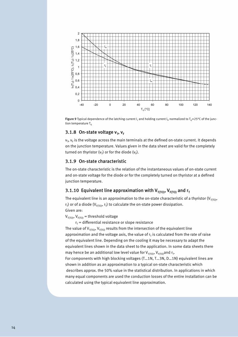
3.1.5 Holding current IH
IH is the minimum value of on-state current required to maintain the thyristor in on-state. IH drops with raising junction temperature (see Figure 9).Light triggered thyristors show a significantly lower holding current than comparable electrically triggered thyristors.
3.1.6 Latching current IL
IL is the on-state current required to maintain the thyristor in the on-state once the gate current has decayed. It depends on the rate of change, peak and duration of the gate current as well as on the junction temperature (see Figure 9).Exception: Light triggered thyristors show a significantly lower latching current than comparable electrically triggered thyristors.
3.1.7 On-state current iT, ITAV, ITRMS iF, IFAV, IFRMS
The on-state current is the current which flows via the main terminals in the on-state of the thyristor (iT, ITAV, ITRMS) or the diode (iF, IFAV, IFRMS). It is differentiated in:iT, iF = instantaneous valueITAV, IFAV = average valueITRMS, IFRMS = RMS (route mean square)
14
3.1.8 On-state voltage vT, vF
vT, vF is the voltage across the main terminals at the defined on-state current. It depends on the junction temperature. Values given in the data sheet are valid for the completely turned on thyristor (vT) or for the diode (vF).
3.1.9 On-state characteristic
The on-state characteristic is the relation of the instantaneous values of on-state current and on-state voltage for the diode or for the completely turned on thyristor at a defined junction temperature.
3.1.10 Equivalent line approximation with VT(TO), VF(TO) and rT
The equivalent line is an approximation to the on-state characteristic of a thyristor (VT(TO), rT) or of a diode (VF(TO), rT) to calculate the on-state power dissipation. Given are:VT(TO), VF(TO) = threshold voltage rT = differential resistance or slope resistanceThe value of VT(TO), VF(TO) results from the intersection of the equivalent line approximation and the voltage axis, the value of rT is calculated from the rate of raise of the equivalent line. Depending on the cooling it may be necessary to adapt the equivalent lines shown in the data sheet to the application. In some data sheets there may hence be an additional low level value for VT(TO), VF(TO)and rT.For components with high blocking voltages (T…1N, T…3N, D…1N) equivalent lines are shown in addition as an approximation to a typical on-state characteristic which describes approx. the 50% value in the statistical distribution. In applications in which many equal components are used the conduction losses of the entire installation can be calculated using the typical equivalent line approximation.
Figure 9 Typical dependence of the latching current IL and holding current lH normalized to Tvj=25°C of the junc-tion temperature Tvj
Technischer Erläuterungen - Bilder
0
0,2
0,4
0,6
0,8
1
1,2
1,4
1,6
1,8
2
-40 -20 0 20 40 60 80 100 120 140Tvj [°C]
I H(T
vj) /
I H(2
5°C
), I L(
T vj)
/ IL(
25°C
) IH
ILIL
IH
Abb./Fig.9 Typische Tvj - Abhängigkeit des auf 25°C normierten Einraststroms IL und Haltestroms IH

15
3.1.11 Maximum average on-state current ITAVM, IFAVM
ITAVM, IFAVM is the maximum permissible continuous average value of the on-state current in a single phase half-wave resistive load circuit according to DIN VDE 0558, part 1 rated at a defined case temperature TC and a frequency of 40 to 60Hz.A diagram is given in the data sheets of the thyristors or diodes with low blocking voltages which shows the maximum average on-state current versus the maximum allowable case temperature TC for various current conduction angles. This diagram takes only the conduction losses into account. For components with high blocking voltages (>2200V) additional turn-off losses and to some degree blocking and turn-on losses need to be considered. For components with very high blocking voltages (>4kV) this diagram is, therefore, omitted in the data sheet.
3.1.12 Maximum RMS on-state current ITRMSM, IFRMSM
ITRMSM, IFRMSM is the maximum value of RMS on-state current permissible considering electrical and thermal stresses of all assembly parts of the device. This current must not be exceeded for flat base and stud type cases and modules even under the best cooling conditions of the thyristor (ITRMSM) or the diode (IFRMSM).
3.1.13 Overload on-state current IT(OV), IF(OV)
IT(OV), IF(OV) is the maximum allowable value of on-state current that the thyristor (IT(OV)) or the diode (IF(OV)) may conduct in short time operation without losing its control property. In the diagram for overload on-state current it is given as the peak value at 50Hz sinusoidal half-waves for different preloads versus time t.This illustration does not take into account increased blocking or turn-off losses as they occur for devices with high blocking voltages. For components with very high blocking voltages (>4kV) this diagram is, therefore, omitted in the data sheet.
3.1.14 Maximum overload on-state current IT(OV)M, IF(OV)M
IT(OV)M, IF(OV)M is the value of on-state current at which the device must be turned off in order not to destroyed the thyristor (IT(OV)M) or the diode (IF(OV)M). These values are intended for the design of the protection networks. The thyristor may temporarily lose its forward blocking capability when the current flowing through it reaches this value and may temporarily lose its control properties. The maximum overload on-state current characteristic shows this value as the peak value of a 50Hz sinusoidal half-wave versus time t. Two conditions are differentiated: no load operation preceding and operation with maximum average on-state currents preceding.
Figure10 Example of an on-state characteristic and the matching equivalent line approximation
0
500
1000
1500
2000
2500
3000
3500
4000
0 0,5 1 1,5 2 2,5 3 3,5
vT [V]
iT [A
]
0
500
1000
1500
2000
2500
3000
3500
4000
0 0,5 1 1,5 2 2,5 3 3,5
vT [V]
iT [A
] ΔiT
ΔvT
rT =ΔiTΔvT
vT0

16
The maximum overload on-state current characteristics given in the individual data sheet applies to a reverse blocking voltage of 80% of the repetitive peak reverse voltage. In cases where the actual reverse voltage is lower, a higher maximum overload on-state current is allowable which is shown in Figure 11 and Figure 12 for a preceding continuous maximum overload on-state current ITAVM. The conditions for a device without preceding load can not be determined from this.This illustration does not take into account increased blocking or turn-off losses as they occur for devices with high blocking voltages. For components with very high blocking voltages (>4kV) this diagram is, therefore, omitted in the data sheet. The protection concepts for these devices are described in chapter 7.2.
Figure 11 Typical dependence of the maximum overload on-state current IT(OV)M, IF(OV)M (in relation to the surge current ITSM or IFSM for 10ms and Tvj max) on the number of half-sinewaves at 50Hz. Parameter: reverse blocking voltage VRM
Figure 12 Typical dependence of the maximum overload on-state current IT(OV)M, IF(OV)M (in relation to the surge current ITSM or IFSM for 10ms and Tvj max) on the time t for a number of half-sinewaves at 50Hz. Param-eter: reverse blocking voltage VRM
Technischer Erläuterungen - Bilder
0-50 V0,33 VRRM
0,67 VRRM
0
0,1
0,2
0,3
0,4
0,5
0,6
0,7
0,8
0,9
1
0 20 40 60 80 100 120 140 160 180 200 220 240 260 280 300t [ms]
I T(O
V)M
/ ITS
M VRM =
Abb./Fig.10 Typische Abhängigkeit des auf ITSM normierten Grenzstroms IT(OV)M von t für mehrere 50Hz Halbwellen Paramter: VRM

17
3.1.15 Surge on-state current ITSM, IFSM
ITSM, IFSM is the maximum permissible peak value of a single half sine-wave 50Hz current pulse. It is specified at 25°C (equates to a short circuit from no load condition) or at turn-on at maximum permissible junction temperature (equates short circuit after permanent load with maximum permissible current). When stressing a semiconductor with the surge on-state current, the device loses its blocking capability. Therefore, no negative voltage shall subsequently be applied. This stress may be repeated during fault conditions in a non-periodic way provided the junction temperature has drop-ped to values within the permissible operating temperature area.When exceeding the maximum permissible value destruction of the device is risked (for details please see chapter 7.2 over current protection).
3.1.16 Maximum rated value ∫i²dt
∫i²dt is the square of the surge on-state current integrated over time. The maximum rated ∫i²dt-value serves to determine the short-circuit protection (see 7.2). For half-sinewaves with periods shorter than 10ms the maximum rated ∫i²dt-value is shown in Figure 13. Regard-ing voltage stress and repetition the same applies as for the surge on-state current. When exceeding the maximum permissible value, destruction of the device is risked. In addition, in particular for large diameter thyristors, it has to be observed that the permissible critical turn-on current rate of change (di/dt)cr may not be exceeded.
Figure 13 Typical dependence of the òi² dt normalized to the value òi² dt (10ms) on the half-sinewave duration tP
Technischer Erläuterungen - Bilder
Abb./Fig.12 Typische Abhängigkeit des auf i² dt (10ms) normierten Grenzlastintegrals i² dt von der Halbschwingungsdauer tP
a
b
c
0
0,1
0,2
0,3
0,4
0,5
0,6
0,7
0,8
0,9
1
0 1 2 3 4 5 6 7 8 9 10
∫i² d
t ( t P
) / ∫i
² dt (
10m
s)
tP [ms]
Thyristoren / Thyristorsa: PB20, PB34, PB50
TO42, TO48, TSW, TFLb: PB60
TO58c: PB70
≥TO75
Dioden / Diodesb: VDRM,RRM ≥ 1000Vc: VDRM,RRM < 1000V
High Power T…1N, T...3N, D…1N
High Power D…1N, T…1N c:
c: für alle Typen, for all types
c: für alle Typen, for all types
18
3.2 Reverse directionThe reverse direction is the direction from one main terminal to the other in which the thyristor and diode is in a stable high resistance state of operation (direction cathode-anode).If values (voltages and currents) and data in reverse direction are to be distinguished from those in forward direction, then the term “reverse” or “negative” is used. The reverse blocking characteristic of a thyristor or a diode represents the instantaneous values of reverse current and reverse voltage.
3.2.1 Reverse current iR
iR is the current flowing in reverse direction through the main terminal of the thyristor or diode. The reverse current depends on the reverse voltage and the junction temperature Tvj (Figure 7)
3.2.2 Reverse voltage vR
VR is the voltage applied across the main terminals of the thyristor or diode in reverse direction.
3.2.2.1 Repetitive peak reverse voltage VRRM
VRRM is the maximum permissible instantaneous value of repetitive voltages in reverse direction including all repetitive peak voltages. In DC applications a reduction to VR (DC) is necessary. See also section 3.2.2.3.For supply voltage see section 3.1.2.1.
3.2.2.2 Non-repetitive peak reverse voltage VRSM
VRSM is the maximum allowable non-repetitive peak value of a transient voltage in reverse direction which must not be exceeded even for the shortest duration. The value resulting is:For blocking voltages < 800V: VRSM = VRRM + 50V (at Tvj = 25°C ... Tvj max)
For blocking voltages ≥ 800V: VRSM = VRRM + 100V (at Tvj = 25°C ... Tvj max)
3.2.2.3 Direct reverse voltage VR(DC)
VR (DC) is the permanently allowable direct voltage in reverse direction, analogous to forward direct off-state voltage 3.1.2.3.
19
3.3 Control properties of thyristors
3.3.1 Positive gate control
3.3.1.1 Gate current iG
iG is the current flowing through the control path (terminals G – HK). Thyristors shall only be pulse triggered during the forward off-state phase. Positive trigger pulses during the reverse off-state phase will lead to significantly increased off-state losses due to the transistor effects caused. These losses adversely affect the functionality and may lead to destruction. Exception: For light triggered thyristors control pulses during the reverse off-state phase are permissible.
3.3.1.2 Gate voltage VG
VG is the positive voltage across the gate terminal (G) and the cathode (K) or auxiliary cathode (HK).
3.3.1.3 Gate trigger current IGT
IGT is the minimum value of gate current which causes the thyristor to trigger. It depends on the voltage across the main terminals and the junction temperature. At the given value of the gate trigger current all thyristors of a given type will trigger. The gate trigger current increases with lower junction temperature and is thus specified at 25°C.
The trigger pulse generator has to safely exceed the data sheet value IGTmax (see also 3.3.1.8).
Exception: For light triggered thyristors the minimum light power PL is specified which causes all thyristors of a given type to trigger.
3.3.1.4 Gate trigger voltage VGT
VGT is the voltage which occurs across gate terminal and cathode when the gate trigger current IGT flows. It depends on the voltage across the main terminals and the junction temperature. At the given value of the gate trigger voltage all thyristors of a given type will trigger. The gate trigger voltage drops with increasing junction temperature and is thus specified at 25°C. VGT is measured when a specified load current flows.
3.3.1.5 Gate non-trigger current IGD
IGD is the value of the gate current which does just not cause the thyristor to trigger. It depends on the voltage across the main terminals and the junction temperature. At the given maximum value no thyristor of a given type triggers. The gate non-trigger current decreases with increasing junction temperature and is thus specified at Tvj max.
3.3.1.6 Gate non-trigger voltage VGD
VGD is the value of the gate voltage which does just not cause the thyristor to trigger.It depends on the voltage across the main terminals and the junction temperature. At the given maximum value no thyristor of a given type triggers. The gate non-trigger voltage decreases with increasing junction temperature and is thus specified at Tvj max.

20
3.3.1.7 Control characteristic
It shows the limits of statistical distribution of the input characteristics of a thyristor type. Within the distribution of the input characteristics the temperature dependent trigger areas are detailed as well as the curves of the maximum permissible gate power dissipation PGM (a – 20W / 10ms, b – 40W / 1ms, c – 60W / 0.5ms).
3.3.1.8 Control circuit
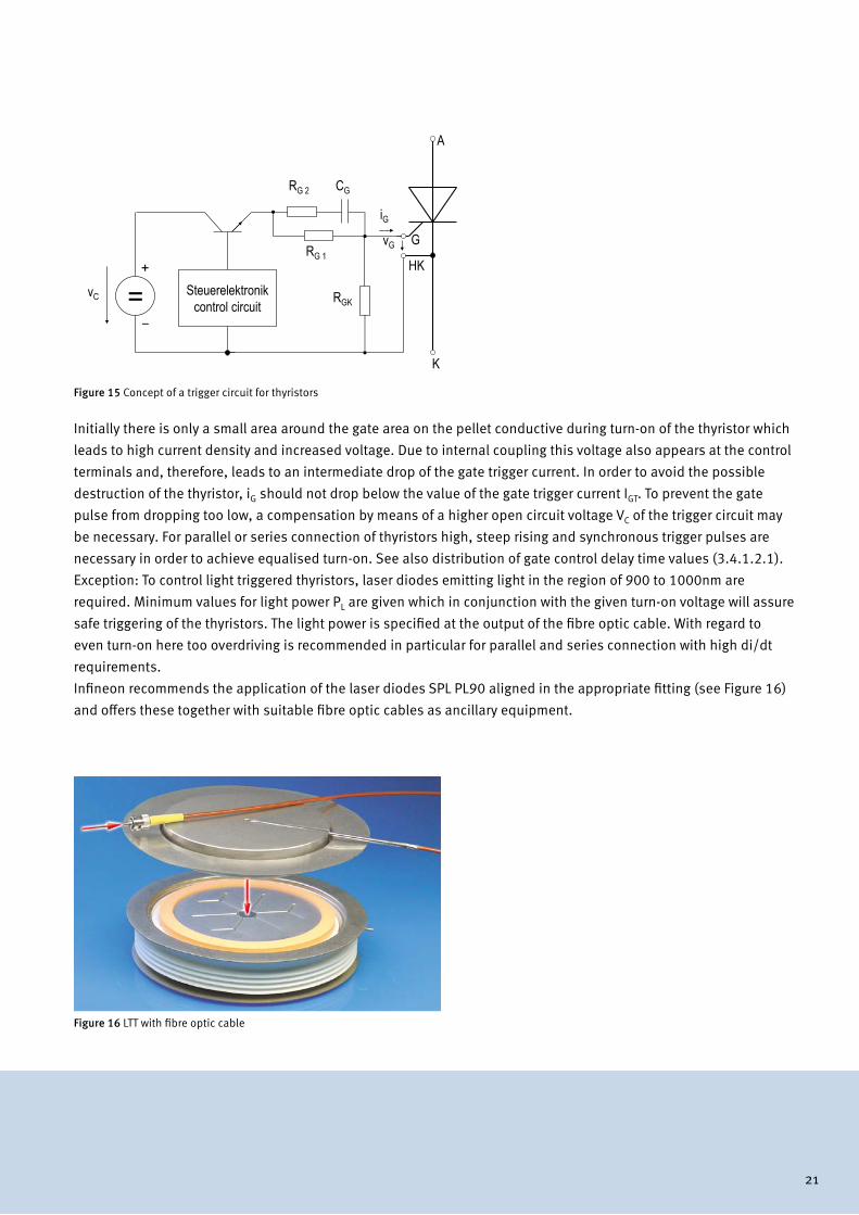
In a normal application the design of the control circuit should be done in accordance with the control data which are detailed in connection with the critical rise time of the on-state current, the gate control delay time and the latching current (see Figure 15). The minimum control data given in 3.3.1.3 and 3.3.1.4 are valid only for applications with low requirements with regard to critical current rise time and gate control delay time. In reality overdriving IGT specified in the data sheet 4- to 5-fold assures safe operation even with high requirements for current rise time and gate control delay time.Terms used in this context are:
diG/dt = gate current slew rateiGM = peak gate currenttG = duration of the trigger pulseVL = open circuit voltage of the control circuitWith increasing slew rate of the on-state current diT/dt as well as repetitive turn-on current IT(RC)M from the snubber an effect from the load circuit to the gate current iG is notable (see 3.4.1.2 and Figure 21).
Figure 14 Example for control characteristic vG = f (iG) with trigger area for VD = 12 V
Technischer Erläuterungen - Bilder
0,1
1
10
100
10 100 1000 10000iG [mA]
v G [V
]
T vj =
+1
25°C
T vj =
-40
°C
T vj =
+2
5°C
ab
c
Abb./Fig.13 Steuercharakteristik vG = f (iG) mit Zündbereichen für VD = 12 V
21
Initially there is only a small area around the gate area on the pellet conductive during turn-on of the thyristor which leads to high current density and increased voltage. Due to internal coupling this voltage also appears at the control terminals and, therefore, leads to an intermediate drop of the gate trigger current. In order to avoid the possible destruction of the thyristor, iG should not drop below the value of the gate trigger current IGT. To prevent the gate pulse from dropping too low, a compensation by means of a higher open circuit voltage VC of the trigger circuit may be necessary. For parallel or series connection of thyristors high, steep rising and synchronous trigger pulses are necessary in order to achieve equalised turn-on. See also distribution of gate control delay time values (3.4.1.2.1).Exception: To control light triggered thyristors, laser diodes emitting light in the region of 900 to 1000nm are required. Minimum values for light power PL are given which in conjunction with the given turn-on voltage will assure safe triggering of the thyristors. The light power is specified at the output of the fibre optic cable. With regard to even turn-on here too overdriving is recommended in particular for parallel and series connection with high di/dt requirements. Infineon recommends the application of the laser diodes SPL PL90 aligned in the appropriate fitting (see Figure 16) and offers these together with suitable fibre optic cables as ancillary equipment.
Figure 16 LTT with fibre optic cable
Figure 15 Concept of a trigger circuit for thyristors
Technischer Erläuterungen - Bilder
Abb./Fig.14 Prinzipschaltbild eines Steuergenerators für Thyristoren
Steuerelektronikcontrol circuit=
+
–
vC
RG 2
iGvG
HK
K
A
G
RGK
RG 1
CG

22
The laser diodes SPL PL 90 comply with the following laser classes:If the laser diode is correctly terminated with the fibre optic cable the control system complies with laser class 1. No operational hazard.With open operation of the laser diode or in case of a broken fibre optic cable, the system equates to the laser class 3b according to IEC 60825–1. In this case hazard of operation exists due to invisible radiation. Direct or indirect exposure to the eyes or skin is to be avoided.
Figure 17 Laser diode SPL PL 90 typical dependence of the light power on the control current
To control light-triggered thyristors, we recommend a current pulse for the laser diode SPL PL90 as in Figure 18. As the laser diode SPL PL90 is not suitable for long-term control, we recommend controlling the laser diode with a frequency of approximately 6kHz, while using the pulse in Figure 18.
Technischer Erläuterungen - Bilder
Abb./Fig.16 Laserdiode SPL PL 90 typ. Abhängigkeit der Lichtleistung vom Steuerstrom
0
50
100
150
200
250
500 600 700 800 900 1000 1100 1200 1300 1400ILaserdiode [mA]
PL [
mW
]

23
3.3.1.9 Minimum duration of the trigger pulse tgmin
The trigger pulse has to be applied at least until the latching current of the thyristor (3.1.6) has been exceeded, as otherwise the thyristor will return to its off-state. The gate trigger current of the thyristor must remain at least at its rated value until the end of the trigger pulse.In applications with very low current rise times or low load currents often a trigger profile with multiple pulses is used (e.g. with a frequency of repetition of 6kHz).For light triggered thyristors make sure that when using multiple pulses the laser diode does not heat up inadmissibly. The light power of a current controlled laser diode drops with increasing temperature.
3.3.1.10 Maximum permissible peak trigger current
In applications with a high rate of rise of current iGT may be overdriven even harder than described in 3.3.1.8. For this the gate current should be increased for a time tGM ≈ 10-20µs to the 8- to 10-fold value of IGT and than continue for a sufficient time tG with a reduced amplitude. The open circuit voltage of the trigger circuit should at least apply 30V in order to assure a high reactionless gate current.
Figure 18 Recommended current pulse for laserdiode SPL PL 90

24
3.4 Carrier storage effect and switching characteristicsWhen the state of operation changes in power semiconductors, the stationary values of current and voltage do not change immediately due to the carrier storage effect. Additionally, in thyristors only small areas around the gate structure become conductive when triggered. The switching losses resulting from this have to be dissipated as heat from the semiconductor.
3.4.1 Turn-on
3.4.1.1 Diode
When passing from a non-conducting or blocked state to a conducting state, voltage peaks occur at the diode due to the carrier storage effect (see Figure 20).
Figure 19 Safe overdrive of the gate trigger current
Figure 20 Schematic representation of a diode turn-on process
Technischer Erläuterungen - Bilder
Abb./Fig.17 Zeitlicher Verlauf des empfohlenen Gateimpulses
tGM
iGIGM ≈ 8-10 IGT
IG ≈ 2-4 IGT
100µs < tG< tP t
0.5-1µsIGM≤
Technischer Erläuterungen - Bilder
VF, iFVFRM
90%
50%
0,1 vF
IFM
ttfr
diF/dt
vF
Abb./Fig.18 Schematische Darstellung des Einschaltvorgangs von Dioden

25
3.4.1.1.1 Peak value of the forward recovery voltage VFRM
VFRM is the highest voltage value occurring during the forward recovery time (see Figure 20). It increases with rising junction temperature and current slew rate.In mains operation (50 / 60Hz) with its moderate current slew rates VFRM is negligible. In self-commutated converters with fast switches di/dt>>1000A/us (IGBT’s, GTO’s and IGCT’s), however, it may reach values up to several hundred volts. Although the forward recovery voltage exists for just a few microseconds and thus does not contribute to the sum of losses of the diodes in a significant way, its effect on the switching semiconductor has to be considered when designing the converter.In diagrams for diodes optimized for these applications data is included which details the forward recovery voltage as a function of the current slew rate.
3.4.1.1.2 On-state recovery time tfr
According to DIN IEC 60747-2 tfr is the time the diode needs to become fully conducting and a static on-state voltage vF appears, when suddenly switched from zero to a defined on-state (see Figure 20).
3.4.1.2 Thyristor
The turn-on process is initiated at forward off-state voltage vD by a gate current with a slew rate diG/dt and a magnitude iGM. For light triggered thyristors this applies to an equally specified trigger pulse on the laser diode.During the gate controlled delay time tgd the blocking voltage across the thyristor drops to 90% (see Figure 21).As initially only a small area around the gate structure becomes conductive, the initial current density and thus the critical rate of rise of on-state current (di/dt)cr is a gauge for the robustness of the thyristor during turn-on.
Figure 21 Schematic representation of a thyristor turn-on process a - gate current with turned off load circuit b - gate current with steeply rising on-state current (see also 3.3.1.8)
Technischer Erläuterungen - Bilder
Abb./Fig.19 Schematische Darstellung des Einschaltvorgangs von Thyristoren
100%90%
50%
10%
ITM
diT/dt iT
vT
t
iT vT
Hauptstromkreismain circuit
90%50%10%
t
iG diG/dt
tgd
Steuerstromkreisgate circuitb
a
Steuergeneratorgate trigger generator
CvCC
L R
iT, vT iG
A
KG
IGM

26
3.4.1.2.1 Gate controlled delay time tgd
tgd is the period between the gate current reaching 10% of its maximum value IGM and the time when the anode-cathode voltage drops below 90% of the applied forward off-state voltage vD (see Figure 21).It reduces significantly with increasing gate current (light power for LTTs) (see Figure 22). In high power thyristors the tgd depends also on vD.
The value given in the data sheet is defined according to DIN IEC 60747 – 6 and is valid for Tvj = 25°C and specified trigger pulse.
3.4.1.2.2 Critical rate of rise of the on-state current (di/dt)cr
Once the voltage has collapsed due to the thyristor triggering a small area of the cathode around the gate structure begins to conduct on-state current. This current conducting area then spreads out depending on the current density with a speed of typically 0.1mm/µs. The current carrying capability of the system is therefore limited in the beginning. Damage or destruction of the thyristor is impossible, however, when the value given in the data sheet for the critical current slew rate is not exceeded. For S-thyristors and thyristors with large square sections the gate is distributed (finger structure). Therefore, these types show a higher (di/dt)cr.
According to DIN IEC 60747 – 6 the critical current rise time (di/dt)cr refers to loading with on-state current over the period of a dampened half sine-wave. It is defined as the angle of a straight line through the 10% and 50% points of the rising on-state current (see Figure 21, Figure 47) whilst the following conditions apply:Junction temperature Tvj = Tvj max
Forward off-state voltage vD = 0.67 VDRM,Peak current value iTM = 2 ITAVM
Frequency of repetition f0 = 50 Hz
Figure 22 Typical dependence of the gate controlled delay time tgd and the maximum gate current iGM
a) maximum value b) typical value
0,1
1
10
100
1000
10 100 1000 10000iGM [mA]
t gd
[µs]
a
b
iGM=iGTiGM=4-5* iGT

27
The trigger pulse is defined in the individual data sheets (see also 3.3.1.8).Exception: Light triggered thyristors are tested with a forward off-state voltage of vD = VDRM.
3.4.1.2.3 Repetitive turn-on current IT(RC)M
IT(RC)M is the maximum permissible peak value of the on-state current immediately after turn-on with undefined rate of rise. In general this turn-on current is caused by the discharge of the RC-snubber network. The maximum permissible repetitive turn-on current also applies to the following steep current rise up to the critical rate of rise of the on-state current (di/dt)cr.For Infineon components the following values applyIT(RC)M = 100A
Exception: Component with the type designation T…1N or T…3NIT(RC)M = 150A
For applications above 60Hz the values for both the critical current rise time (di/dt)cr as well as the repetitive turn-on current IT(RC)M have to be reduced. Further details for particular conditions on request.
3.4.1.2.4 Critical rate of rise of off-state voltage (dv/dt)cr
(dv/dt)cr is the maximum value for the rate of rise of a voltage applied in forward direction running almost linearly from 0% to 67% of VDRM at which a thyristor will not switch to the on-state. For an exponential rate of voltage rise it is a line which crosses the exponential function starting from 0% to 63% of the maximum value.It applies for open trigger circuit and maximum permissible junction temperature. Exceeding (dv/dt)cr may cause destruction.
Exception: Aside from the over-voltage protection (BOD) light triggered thyristors have an integrated dv/dt protec-tion. This causes the thyristors to trigger safely over the entire gate structure when the dv/dt gets to high.
3.4.2 Turn-off
Turning off is usually started by application of a reverse voltage. The load current of the thyristor or the diode does not cease at the zero crossing but continues to flow briefly in reverse direction as reverse recovery current until the carriers have left the junction region.The softness factor FRRS describes the relation of the rates of rise of the currents during the turn-off process.
3.4.2.1 Recovery charge Qr
Qr is the total amount of charge flowing out of the semiconductor after switching from on-state to reverse off-state. It increases with rising junction temperature as well as magnitude and fall time of the on-state current. If not otherwise specified, the given values are valid for vR = 0.5VRRM and vRM = 0.8VRRM and are not exceeded by 95% of the individual types of thyristors or diodes. For this an appropriately designed RC-snubber network is specified.For components with the type designation T…1N, T…3N and D…1N the given values in the data sheet are maximum values which are 100% tested in production. The recovery charge Qr is mainly dependent on the junction temperature Tvj and on the rate of fall of the decaying current (see Figure 24 and Figure 25).

28
Figure 23 Schematic representation of the thyristor and diode turn-off process
Figure 24 Typical Tvj-dependence of the recovery charge Qr normalized to Qr(Tvj max)
Figure 25 Typical di/dt-dependence of the recovery charge Qr normalized to Qr(di/dt=10A/µs)
Technischer Erläuterungen - Bilder
Abb./Fig.21 Typische Tvj-Abhängigkeit der auf Qr(Tvj max) normierten Sperrverzögerungsladung Qr
0,6
0,7
0,8
0,9
1,0
1,1
-80 -60 -40 -20 0 20Tvj = Tvj -Tvj max [°C]
Qr (
T vj) /
Qr (
T vj m
ax)
0
0,2
0,4
0,6
0,8
1
1,2
0 1 2 3 4 5 6 7 8 9 10 11
di/dt [A/µs]
Qr (
di/d
t) /
Qr (
di/d
t=10
A/µs
)
Technischer Erläuterungen - Bilder
Abb./Fig.20 Schematische Darstellung des Ausschaltvorgangs von Thyristoren und Dioden
ITM , IFM
-di/dtIRM vRM
vR
trrvT , vF Qr
0,25 IRM
0,9 IRM
i , v
t
dir/dt
tint
tp
dtdi
dt-di
rFRRS

29
3.4.2.2 Peak reverse recovery current IRM
IRM is the maximum value of the reverse recovery current. The dependences and operating conditions given for Qr also apply. If IRM is not shown in the diagrams, its value may be approximately determined as follows:
Figure 26 Typical Tvj-dependence of the peak reverse recovery current IRM normalized to IRM (Tvj max)
Figure 27 Typical di/dt-dependence of the peak reverse recovery current IRM normalized to IRM (di/dt=10/µs)
For components with the type designation T…1N, T…3N and D…1N the given values in the data sheet are maximum values which are 100% tested in production. The peak reverse recovery current IRM is mainly dependent on the junction temperature Tvj and on the rate of fall of the decaying current (see Figure 26 and Figure 27).
Technischer Erläuterungen - Bilder
Abb./Fig.22 Typische Tvj-Abhängigkeit der auf IRM (Tvj max) normierten Rückstromspitze IRM
0,6
0,7
0,8
0,9
1,0
1,1
-80 -70 -60 -50 -40 -30 -20 -10 0 10 20Tvj = Tvj - Tvj max [°C]
I RM (T
vj) /
I RM (T
vj m
ax)
0
0,2
0,4
0,6
0,8
1
1,2
0 1 2 3 4 5 6 7 8 9 10 11
di/dt [A/µs]
I RM
(di/
dt) /
I RM
(di/
dt=
10A/
µs)
RM
r
I-di/dt Q
1...1,3
⋅
RM
r
I-di/dt Q
1...1,3
⋅t
2 Q
Irrr
RM
≈⋅

30
3.4.2.3 Reverse recovery time trr
trr is the time interval between the zero crossing of the current and the time at which a straight line through the 90% and 25% points of the decaying reverse recovery current crosses the zero line (see Figure 23 ). Should trr not be specified, its value may be approximately calculated with the following formula:
3.4.2.4 Turn-off time tq
tq is the time interval between the zero crossing of the current commutated in reverse direction and the reapplication of forward off-state voltage at which a thyristor does not turn-on without a control pulse. The actual pause time realised in the application before the forward off-state voltage reoccurs is called hold-off time. This time must always be greater than the turn-off time. The turn-off time mainly depends on the fall time of the on-state current, the rate of rise of the forward off-state voltage and the junction temperature (see Figure 29 - Figure 31). To determine tq the duration tP of the forward current has to be chosen long enough so that the thyristor at the point of commutation is completely turned on (see Figure 28). The values given in the data sheets are valid for following conditions:
Junction temperature Tvj = Tvj max
Magnitude of on-state current iTM ≥ ITAVM
Fall rate of the on-state current -diT/dt = 10 A/µsReverse voltage VRM = 100VRate of rise of the forward off-state voltage dvD/dt = 20V/µsForward off-state voltage VDM = 0.67VDRM
Exception: Fast thyristors were commutated off with a current rate of fall of –di/dt=20A/µs. The dvD/dt may vary here and is specified by the 5th letter in the type designation (see section 2.3).
For phase controlled thyristors usually typical values for the turn-off time are given as they are mainly employed in line commutated converters. In these applications the hold-off time is generally much longer than the turn-off time of the thyristor.If the hold-off time is shorter than the turn-off time, the thyristor will once again turn-on with rising forward off-state voltage without application of a trigger pulse and destruction may be caused (tq-limit values on request if necessary).
t2 Q
Irrr
RM
≈⋅

31
If the thyristor is operated together with an inverse diode (for example free wheeling diode), much longer turn-off times have to be taken into consideration due to the low commutation voltage (typically 30% longer). Additionally, in such applications the inductance of the free wheeling circuit should be minimised as otherwise the turn-off time may increase to significantly higher values.
Figure 28 Schematic representation of the turn-off behaviour of a thyristor
Figure 29 Typical dependence of the turn-off time tq normalized to Tvj max on the junction temperature Tvj
t P t q VDMdvD/dt63%50% t-diT/dtVRM tITM
vDiTvRiR vT vR
Technischer Erläuterungen - Bilder
Abb./Fig.23 Schematische Darstellung vom Ausschalten und Freiwerden eines Thyristors
t P
t qVDM
dvD/dt
63%
50%
t
-diT/dt
VRM
t
ITM
vD
iT
vR
iR
vT
vR
Technischer Erläuterungen - Bilder
Abb./Fig.24 Typische Tvj-Abhängigkeit der auf tq(Tvj max) normierten Freiwerdezeit tq
0,4
0,5
0,6
0,7
0,8
0,9
1
1,1
1,2
-80 -70 -60 -50 -40 -30 -20 -10 0 10 20Tvj = Tvj - Tvj max [°C]
t q (T
vj) /
t q (T
vj m
ax)

32
Figure 30 Typical dependence of the turn-off time tq normalized to the -diT/dtnorm on the off-commutating rate of fall -diT/dt
Figure 31 Typical dependence of the turn-off time tq normalized to the dvD/dt = 20V/µs on the rate of rise of off-state voltage dvD/dt
Technischer Erläuterungen - Bilder
Abb./Fig.25 Typische diT/dt-Abhängigkeit der auf tq(diT/dtnorm) normierten Freiwerdezeit tq
0,9
1,0
1,1
1,2
1,3
0 1 2 3 4 5 6 7 8 9 10-diT/dt / -diT/dtnorm
t q(-d
i T/dt
) / t q
(-di
T/dt n
orm)
-diT/dtnorm:N-Thyristor: 10A/µs S-Thyristor: 20A/µs
0,7
0,8
0,9
1,0
1,1
1,2
0 5 10 15 20
t q(-
di T
/dt)
/ t
q(-
di T
/dt=
10A
/s)
-diT/dt [A/ s]
Technischer Erläuterungen - Bilder
Abb./Fig.26 Typische duD/dt-Abhängigkeit der auf tq(duD/dt = 20V/µs) normierten Freiwerdezeit tq
0,9
1
1,1
1,2
1,3
1,4
1,5
1,6
1,7
1,8
0 100 200 300 400 500dvD/dt [V/µs]
t q (d
v D/d
t) / t
q (dv
D/d
t=20
V/µs
)

33
3.5 Power dissipation (losses)For thyristor and diode the dissipation (or losses) are classified as off-state, on-state, turn-on and turn-off losses. The thyristor also shows control losses. Under given cooling conditions their sum determines the current loading capability.For mains operation up to 60Hz with its moderate dynamic requirements the dimensioning can be exclusively done based on the on-state losses, as the sum of the others is comparatively negligible. For semiconductors with high blocking voltages (> 2200V) or large square sections with a pellet Ø ≥ 80mm even for mains operation the turn-off losses should be regarded in the calculation.
3.5.1 Total power dissipation Ptot
Ptot is the average value of the sum of the individual losses.
3.5.2 Off-state losses PD, PR
PD, PR are the losses caused by off-state current and off-state voltage in forward direction (PD) and in reverse direction (PR).
3.5.3 On-state losses PT, PF
PT, PF is the electric power converted to heat when only the conducting state in forward direction is considered. The average value of the on-state loss PTAV or PFAV is calculated with the values of the equivalent straight line according to the following formula:
PTAV = VT(TO) • ITAV + rT • I²TRMS= VT(TO) • ITAV + rT • I²TAV • F² (for thyristors) PFAV = VF(TO) • IFAV + rT • I²FRMS= VF(TO) • IFAV + rT • I²FAV • F² (for diodes)
For formfactors F refer to Table 1
The diagrams in the data sheets show the relation of the average value of on-state dissipation power and on-state current for various shapes of current.
Instead of calculating the on-state losses with vT0, vF0 and rT, alternatively the on-state voltage can be calculated with a more precise approximation with the following relation:
The factors A, B, C and D are listed in the datasheets.
Exception: PowerBLOCK-Modules are not listed with the ABCD coefficients.
v = A + B i + C Ln( i + 1) + D iT T T T
⋅ ⋅ ⋅

34
3.5.4 Switching losses PTT, PFT+PRQ
PTT, PFT+PRQ are the portions of electric power converted to heat when turning on (PTT for thyristors, PFT for diodes) and turning off (PRQ). The average switching losses increase with increasing rates of rise and fall of the on-state current at turn-on and turn-off as well as with the frequency of repetition. Up to medium size thyristors and diodes with blocking voltages up to 2200V and applications at mains frequencies of up to 60Hz the switching losses are mostly negligible compared to the on-state losses. For semiconductors with high blocking voltages > 2200V or large square sections with a pellet Ø ≥ 80mm even for mains operation the turn-off losses should be regarded in the calculation (on request if necessary). The turn-off losses of diodes, however, are generally still negligible.
3.5.4.1 Turn-on losses PTT, PFT
PTT, PFT is that dissipative portion which exceeds the on-state loss PT (for thyristors) or PF (for diodes) during turn-on. It is caused on the one hand by the carrier storage effect and on the other hand by the delayed propagation of the current carrying area.To be able to turn on with the greatest possible square section many thyristors are equipped with trigger amplification. This consist of one or several amplifying gates (= auxiliary thyristors). In thyristors with large square sections the amplifying gate is branched (finger structure). This causes a wider area to become conductive at the time of triggering and thus reduces the turn-on losses.
Table 1 Form factors for phase angle control conditions
Stromform Scheitelfaktor Mittelfaktor Formfaktor Formfaktor²Current waveform peak factor average factor form factor form factor²
sinus 180° el 2 π = 3,14 π / 2 = 1,57 2,47
sinus 120° el 2,23 4,18 1,875 3,52
sinus 90° el 2,83 6,29 2,22 4,93
sinus 60° el 3,88 10,9 2,77 7,66
sinus 30° el 5,88 23,42 3,98 15,8
DC 1 1 1 1
rect 180° el 2 2
rect 120° el 3 3
rect 90° el 4 4
rect 60° el 6 6
rect 30° el 12 12
2FRMSIiS =
AVIiM =
AV
RMS
IIF =
41,12 =
45,26 =
46,312 =
73,13 =
24 =
41,12 =
45,26 =
46,312 =
73,13 =
24 =
0° 0 180°
0° 0 180°

35
The sum of turn-on and on-state losses PTT, PFT + PT, PF important for the dissipation calculation may be drawn from the progression of the on-state current and the on-state voltage during and after turning on.
(for thyristors)
(for diodes)
In practice the turn-on losses are generally neglected.
3.5.4.2 Turn-off losses PRQ
Turn-off losses occur due to the carrier storage effect. They depend on the progression of the reverse delay current as well as on the magnitude and rate of rise of the reverse off-state voltage and may therefore be influenced by the snubber (see Figure 23 ).
For the time period tint to be determined by integration the turn-off losses are calculated as follows:An approximation of the turn-off losses may be calculated as follows:
PRQ = ERQ * f ≈ Qr * vR * 0.4 * f for the on-state limit characteristicPRQ = ERQ * f ≈ Qr * vR * 0.5 * f for the typical on-state characteristic
ERQ = turn-off loss energyf = frequency Qr = maximum recovery chargevR = (reverse voltage) driving voltage after commutation
3.5.5 Gate dissipation PG
PG is the electrical power converted into heat due the gate current flowing between gate terminal and cathode. This is distinguished into peak gate dissipation PGM (product of the peak values of gate current and gate voltage) and average gate dissipation PGAV (average value of gate dissipation referenced to the cycle duration).
3.6 Insulation test voltage VISOL The insulation test voltage VISOL is the RMS-value of a sinewave voltage between the base plate and the terminal of thyristor or diode modules. For DC-requirements VISOL DC is equal to the peak value of the specified RMS-value (i.e. 1.41* VISOL). During the test all terminals are connected with each other and VISOL is applied versus the base plate.
P =1
ti (t) v (t)dt
RQ
int
R0
t
R
int
⋅∫
P +P =1
ti (t) v (t)dt
TT T
T
T0
t
T
T
⋅∫
P +P =1
ti (t) v (t)dt
FT F
T
F0
t
F
T
⋅∫

36
4. Thermal propertiesIn order to maintain the thermal equilibrium the electric power loss converted to heat in the semiconductors has to be dissipated. For this purpose heatsinks with defined cooling properties are available. To describe this function thermal equivalent circuits, by analogy to electrical ciruits, according to Figure 32 are used.
Rth JC= steady state thermal resistance junction - caseRth CH= steady state transfer thermal resistance case - heatsinkRth HA= steady state thermal resistance heatsink
a - single sided coolingb - double sided cooling
4.1 Temperatures
4.1.1 Junction temperature Tvj, Tvj max
The junction temperature is the most important reference for all fundamental electrical properties. It represents a mean spatial temperature within the semiconductor systems and is, therefore, known more precisely as the equivalent junction temperature or virtual junction temperature.To observe the maximum permissible junction temperature Tvj max is important for the function and reliability of the device. To exceed this maximum value may change the properties of the semiconductor irreversibly and destroy it.
4.1.2 Case temperature TC
TC is the maximum temperature at the contact area of the thyristor or diode case of a disc cell or the base plate of a PowerBLOCK-module.
b
Figure 32 Thermal equivalent circuits for diodes and thyristors
Technischer Erläuterungen - Bilder
Ptot
QW
Tvj
TC
TH
TA
RthHA
RthjC
RthCH
RthCA
QW
Tvj
TC
TH
TA
RthHA[K]
RthCA[A]
RthjC[K]
RthCH[K]
RthCA[K]
TC
TH
RthHA[A]
RthjC[A]
RthCH[A]
Ptot
Tvj
TC
TH
TA
RthHA
RthjC
RthCH
RthCA
a b
Abb./Fig.27 Thermisches Ersatzschaltbild für Dioden und Thyristoren

37
4.1.3 Heatsink temperature TH
TH is the temperature of the heatsink resulting from the semiconductor through the contact area of the heatsink and its surrounding cooling media.The heatsinks offered by Infineon have been tested and specified with components mounted. The heatsink data given, therefore, include the thermal transfer resistance RthCH between device and heatsink. This value can, therefore, be disregarded in the calculation.
4.1.4 Cooling medium temperature TA
TA is the temperature of the cooling medium prior to entering the heatsink. For air cooling this is defined at the inlet side of the heatsink. For fluid cooling it is defined at the inlet of the heatsink.
4.1.5 Junction operating temperature range Tcop
Tcop is the case temperature range in which the power semiconductor may be operated.
4.1.6 Storage temperature range Tstg
Tstg is the temperature range in which the power semiconductor may be stored without the application of electricity.Independently of the maximum permissible junction temperature unlimited in time, the maximum permissible storage temperature for epoxy disc cells and for PowerBLOCK-modules is Tstg = 150°C with a time limit to 672h according to DIN IEC 60747-1.
4.2 Thermal resistances
4.2.1 Internal thermal resistance RthJC
RthJC is the ratio of the difference between the junction temperature Tvj and the case temperature TC to the total power dissipation Ptot:
It depends on the internal design as well as the shape and frequency of the on-state current.The thermal resistance for double sided cooling compared to single sided cooling is lower due to paralleling of the individual thermal resistances (see Figure 32).The thermal resistance depends on the type and shape of the semiconductor. It is therefore not 100% measured, but established instead during the initial type approval qualification tests.
4.2.2 Thermal transfer resistance RthCH
RthCH is the ratio of the difference between the temperature of the contact areas of the device and the heatsink TC – TH to the total power dissipation Ptot:
The values given are valid only when mounted correctly (see section 8).
R =T - T
PthJC
vj C
tot
R =T - T
PthCHC H
tot

38
4.2.3 Heatsink thermal resistance RthCA
RthCA is the ratio of the difference between the case temperature TC and the coolant temperature TA to the total power dissipation Ptot:
4.2.4 Total thermal resistance RthJA
RthJA is the ratio of the difference between the equivalent junction temperature Tvj and the coolant temperature TA to the total power dissipation Ptot:
4.2.5 Transient internal thermal resistance ZthJC
ZthJC describes the progression of the component’s thermal resistance over time. In the data sheets ZthJC is given for constant DC-current and partly also for pulse currents. Additionally, the partial thermal resistances Rthn and time constants tn are compiled in a table as an analytical function.
4.2.6 Transient heatsink thermal resistance ZthCA
ZthCA describes the progression of the heatsink thermal resistance over time. ZthCA is defined in individual data sheets. Additionally, the values RthCAn and tn of the analytical function are compiled in a table. There is no generally defined transient thermal resistance for heatsinks. On the one hand, it depends on the contact region between power semiconductor and heatsink. On the other hand, the cooling method (natural/forced) and the flow of the cooling medium have a strong influence. In case of natural cooling and oil cooling, the flow of the cooling medium is caused by the convection of the air or oil. As the power dissipation defines the convection, the actual power dissipation is specified for natural cooling and oil cooling. The correct direction and position of the heatsink has to be observed.In case of forced cooling and water cooling, the flow of the cooling medium is specified.
Short-term temperature variations due to pulse currents are widely independent of these parameters. They are equalised through the large thermal capacity of the heatsink.
R =T - T
PthCAC A
tot
R =T - T
P=R +R
thJA
vj A
tot
thJC thCA
Z = R (1 -e )(th)JC thn
n=1
n-t t
max
n∑

39
The heatsinks offered by Infineon have been tested and specified with components mounted. These given heatsink data include the transfer thermal resistance RthCH between device and heatsink. This value is, therefore, to be disregarded.
4.2.7 Total transient thermal resistance ZthJA
ZthJA describes the progression of the total thermal resistance over time. The calculation of the junction temperature for short-term loads is to be based on the total transient thermal resistance. ZthJA is the sum of:
ZthJA = ZthJC + ZthCA
4.3 Cooling
4.3.1 Natural air cooling
In natural air cooling (air convection cooling) the power losses are dissipated due to natural convection of the air. Generally the current loading capability of power semiconductors is defined at an ambient temperature TA = 45°C.
4.3.2 Forced air cooling
In forced air cooling the cooling air is forced through the fins of the heatsink by means of a fan. Generally the current carrying capability of power semiconductors is defined at an ambient temperature TA = 35°C.
4.3.3 Water cooling
In water cooling the power losses are dissipated by means of water. Generally, the current loading capability of power semiconductors is defined at an inlet water temperature TA = 25°C.
4.3.4 Oil cooling
In oil cooling the power losses are dissipated by means of oil. Generally, the current loading capability of power semiconductors is defined at an inlet oil temperature TA = 70°C.

40
5. 5. Mechanical properties
5.1 Tightening torque
When mounting PowerBLOCK modules and studs, Infineon recommends keeping the tightening torques as given in the data sheet, as otherwise the correct function within the specifications cannot be guaranteed (see also 8.2).
5.2 Clamping forceThe clamping force given in the data sheet is necessary for perfect electrical and thermal contact of devices with flat base or disc housing. It must be largely homogeneous across the contact surfaces (see also 8).The limits of the clamping force for devices in disc housings are given in the relevant data sheets. These have to be precisely observed. Deviations may alter the data and require special agreement. The clamping force recommended should approximately be in the middle between the given limits.
5.3 Creepage distanceThe creepage distance between anode and cathode or anode and gate is defined according to DIN VDE 0110.
5.4 Humidity classificationThe values given comply with DIN IEC 60721-3 (3K3).
5.5 VibrationThe values given follow DIN IEC 60068, part 2-6.It is given in the data sheet as a multiple of the gravitational constant (1g = 9.81m/s²).
5.6 UL-registrationPowerBLOCK modules normally comply with the standard for electrically insulated semiconductor components of the Underwriters Laboratories Inc.The appropriate file number is listed in the individual data sheets in the section Mechanical Properties.
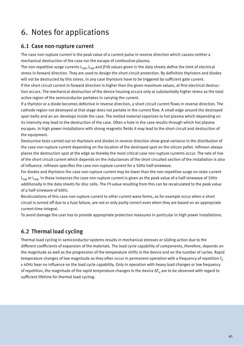
41
6. Notes for applications
6.1 Case non-rupture currentThe case non-rupture current is the peak value of a current pulse in reverse direction which causes neither a mechanical destruction of the case nor the escape of combustive plasma.The non-repetitive surge currents ITSM, IFSM and ∫i²dt values given in the data sheets define the limit of electrical stress in forward direction. They are used to design the short circuit protection. By definition thyristors and diodes will not be destructed by this stress. In any case thyristors have to be triggered by sufficient gate current.If the short circuit current in forward direction is higher than the given maximum values, at first electrical destruc-tion occurs. The mechanical destruction of the device housing occurs only at substantially higher stress as the total active region of the semiconductor partakes in carrying the current. If a thyristor or a diode becomes defective in reverse direction, a short circuit current flows in reverse direction. The cathode region not destroyed at that stage does not partake in the current flow. A small edge around the destroyed spot melts and an arc develops inside the case. The melted material vaporizes to hot plasma which depending on its intensity may lead to the destruction of the case. Often a hole in the case results through which hot plasma escapes. In high power installations with strong magnetic fields it may lead to the short circuit and destruction of the equipment.Destructive tests carried out on thyristors and diodes in reverse direction show great variance in the distribution of the case non-rupture current depending on the location of the destroyed spot on the silicon pellet. Infineon always places the destruction spot at the edge as thereby the most critical case non-rupture currents occur. The rate of rise of the short circuit current which depends on the inductances of the short circuited section of the installation is also of influence. Infineon specifies the case non-rupture current for a 50Hz half-sinewave.For diodes and thyristors the case non-rupture current may be lower than the non-repetitive surge on-state current ITSM or IFSM. In these instances the case non-rupture current is given as the peak value of a half-sinewave of 50Hz additionally in the data sheets for disc cells. The I²t-value resulting from this can be recalculated to the peak value of a half-sinewave of 60Hz.Recalculations of this case non-rupture current to other current wave forms, as for example occur when a short circuit is turned off due to a fuse failure, are not or only partly correct even when they are based on an appropriate current-time-integral.To avoid damage the user has to provide appropriate protection measures in particular in high power installations.
6.2 Thermal load cyclingThermal load cycling in semiconductor systems results in mechanical stresses or sliding action due to the different coefficients of expansion of the materials. The load cycle capability of components, therefore, depends on the magnitude as well as the progression of the temperature shifts in the device and on the number of cycles. Rapid temperature changes of low magnitude as they often occur in permanent operation with a frequency of repetition f0
≥ 40Hz bear no influence on the load cycle capability. Only in operation with heavy load changes or low frequency of repetition, the magnitude of the rapid temperature changes in the device ΔTvj are to be observed with regard to sufficient lifetime for thermal load cycling.
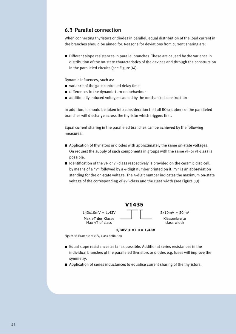
42
6.3 Parallel connectionWhen connecting thyristors or diodes in parallel, equal distribution of the load current in the branches should be aimed for. Reasons for deviations from current sharing are:
n Different slope resistances in parallel branches. These are caused by the variance in distribution of the on-state characteristics of the devices and through the construction in the paralleled circuits (see Figure 34).
Dynamic influences, such as:n variance of the gate controlled delay timen differences in the dynamic turn-on behaviourn additionally induced voltages caused by the mechanical construction
In addition, it should be taken into consideration that all RC-snubbers of the paralleled branches will discharge across the thyristor which triggers first.
Equal current sharing in the paralleled branches can be achieved by the following measures:
n Application of thyristors or diodes with approximately the same on-state voltages. On request the supply of such components in groups with the same vT- or vF-class is possible.
n Identification of the vT- or vF-class respectively is provided on the ceramic disc cell, by means of a “V” followed by a 4-digit number printed on it. “V” is an abbreviation standing for the on-state voltage. The 4-digit number indicates the maximum on-state voltage of the corresponding vT-/vF-class and the class width (see Figure 33)
n Equal slope resistances as far as possible. Additional series resistances in the individual branches of the paralleled thyristors or diodes e.g. fuses will improve the symmetry.
n Application of series inductances to equalise current sharing of the thyristors.
Figure 33 Example of vT/vF class definition
Technischer Erläuterungen - Bilder
V1435143x10mV = 1,43V
Max vT der KlasseMax vT of class
5x10mV = 50mV
Klassenbreiteclass width
1,38V < vT <= 1,43V

43
n Minimal deviation in gate controlled delay time values. To minimise this, triggering of the thyristors with synchronous, steep and high current pulses is required. iGM ≥ 4...10 IGT dG/dt ≥ iGM/(0.5-1µs) The anode-cathode voltage across the paralleled devices drops to the on-state voltage of the first thyristor which triggers. Consequently, the voltage dependent trigger delay of the thyristors turning on later and the start of turn-on of these thyristors is retarded accordingly. This has to be considered in particular for light triggered thyristors as these require a higher anode-cathode voltage to safely turn-on. For high power thyristors (T…1N) the data sheet recommends a trigger pulse with gate controlled delay time. With this, the deviation of the gate controlled delay times tgd may be reduced to values Δtgd < 0.5µs under the listed conditions. In conjunction with the snubber this is generally sufficient for safe triggering of the thyristors which makes additional selection needless. To parallel light triggered thyristors (T…3N) Infineon recommends the use of laser diodes SPL PL90 with the appropriate fibre optic cable and a control pulse for the laser diode of 1.3A for 2µs followed by 0.8A for 8µs (see Figure 18).
n The gate pulses described above also assure that the differences in the dynamic on-state characteristics are minimised.
n In particular for large thyristors and those with high blocking voltages the risk exists that some of these will return to the forward off-state after triggering due to a too low on-state current density. Overloading of the current carrying thyristors after renewed load current increase can be avoided by repetitive triggering.
In general, a current sharing imbalance of less than 10% is aimed for.
Figure 34 Current sharing imbalance due to different on-state voltages in parallel connection
Technischer Erläuterungen - Bilder
Abb./Fig.28 Stromfehlverteilung infolge unterschiedlicher Durchlassspannungen bei Parallelschaltung
Vparallel
I1
I2
vF, vT
I F, I T

44
6.4 Series connectionWhen connecting thyristors or diodes in series, equal distribution of the off-state voltage should be aimed for. Reasons for deviations from the ideal voltage sharing are:n Different leakage currents
Without additional external components, an unfavourable voltage sharing may occur during the steady off-state condition in both directions as the voltage across the individual thyristors or diodes results out of the uniform reverse current in the series circuit (see Figure 35).
n Variance of the gate controlled delay time During turn-on the thyristors triggered last are exposed by higher off-state voltage.
n Variance of the reverse recovery charge Differences of the reverse recovery charge Qr cause different reverse recovery times trr and peak reverse recovery currents IRM which means that the thyristors or diodes take up off-state voltage at different times (see Figure 36 ). The variance of the reverse recovery charge ΔQr of two thyristors or diodes connected in series effects a voltage deviation ΔV ≈ ΔQr/C where C is the capacitor of the parallel snubber circuits (see section 7.1).
Figure 35 Voltage sharing imbalance due to different leakage currents in series connection
Technischer Erläuterungen - Bilder
Abb./Fig.29 Spannungsfehlverteilung infolge unterschiedlicher Sperrströme bei Reihenschaltung
Iseries
V2V1
vD, vR
i D, i
R

45
Equal off-state voltage for thyristors and diodes connected in series may be achieved by the following meaures:n Steady state voltage sharing during the off-state phase
For this the RC-snubber is often sufficient. In case the DC off-state voltage is applied for longer periods, an additional voltage sharing resistor paralleled to each thyristor or diodes is necessary. It should carry about two to five times the leakage current of the applied power semiconductor at operating temperature in order to externally force a steady state voltage symmetry. If the operating temperature is less then the maximum allowable junction temperature for continuous operation, the leakage current drops per 10°C to approx. 66% of the initial value. For example for thyristors with a maximum allowable junction temperature the following applies Tvj max = 125°C: 0.66 ID oR 0.66 IR at Tvj = 115°C 0.44 ID oR 0.44 IR at Tvj = 105°C etc.
n Dynamic voltage sharing at turn-on To reduce the variance of the gate controlled delay times, triggering of electrically triggered thyristors is necessary with synchronous, steep and high trigger pulses. iGM ≥ 4...10 IGT diG/dt ≥ iGM/(0.5-1µs) Such strong trigger pulses reduces the spread of the gate controlled delay time to values Δtgd < 1µs. It has to be ensured that the reverse blocking voltage of the thyristor which is last to turn on (in a series connection)
Figure 36 Voltage sharing imbalance due to different turn-off properties
Technischer Erläuterungen - Bilder
Abb./Fig.30 Spannungsfehlaufteilung infolge unterschiedlichen Ausschaltverhaltens
vT , vF
i , v
t
V= Qr/C
Qr
iT , iF
iR
vR

46
increases only slowly. Often the RC-snubber is sufficient for this. In case the inductance of this circuit working jointly with the RC networks are not sufficient to reduce the reverse voltage increase additional saturable inductances are to be implemented. For high power thyristors (T…1N) a trigger pulse for a gate controlled delay time is recommended in the data sheet. With this or better pulses the variance of the gate control delay times may be reduced to values Δtgd < 0.5µs under the given conditions. For series connection of light triggered thyristors (T…3N) which are exposed to high current rise times Infineon recommends the use of laser diodes SPL PL90 with the appropriate fibre optic cable and a control pulse of 1.3A for 2µs followed by 0.8A for 8µs.
n Dynamic voltage sharing at turn-off During turn-off it is possible to improve the imbalance of off-state voltage sharing both by sufficient dimensioning of the paralleled snubbers as well as by a small variance of the recovery charge ΔQr of the thyristors in series. The supply of thyristors and diodes in groups with the same Qr-class is possible on request.
6.5 Pulsed PowerPulsed power applications are generally applications with very low duty cycle.
To dimension semiconductors for pulsed power applications generally the following has to be observed:
6.5.1 Applications with DC
Often the power semiconductors in pulsed power applications are exposed to high DC-voltages. For this the limitations regarding reduced voltage stress are to be observed (see 3.1.2.3 and 3.2.2.3).
6.5.2 Current rise time at turn-on
Due to the finite propagation in the triggered area (~ 0.1mm/µs) when the thyristor is turned on, the load current is initially concentrated to a small area. If the current density exceeds the critical value, destruction of the device is likely. Therefore the peak current amplitude in short pulse durations drops significantly (see Figure 37).
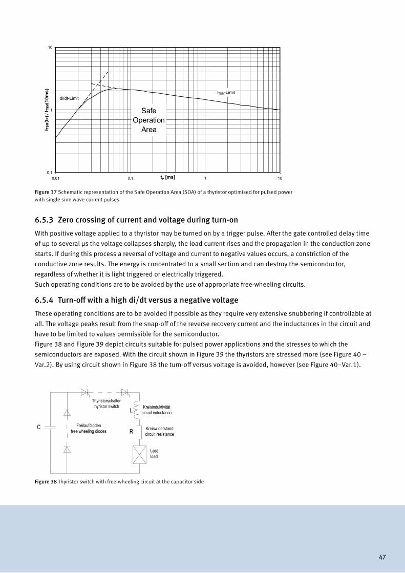
47
6.5.3 Zero crossing of current and voltage during turn-on
With positive voltage applied to a thyristor may be turned on by a trigger pulse. After the gate controlled delay time of up to several µs the voltage collapses sharply, the load current rises and the propagation in the conduction zone starts. If during this process a reversal of voltage and current to negative values occurs, a constriction of the conductive zone results. The energy is concentrated to a small section and can destroy the semiconductor, regardless of whether it is light triggered or electrically triggered. Such operating conditions are to be avoided by the use of appropriate free-wheeling circuits.
6.5.4 Turn-off with a high di/dt versus a negative voltage
These operating conditions are to be avoided if possible as they require very extensive snubbering if controllable at all. The voltage peaks result from the snap-off of the reverse recovery current and the inductances in the circuit and have to be limited to values permissible for the semiconductor.Figure 38 and Figure 39 depict circuits suitable for pulsed power applications and the stresses to which the semiconductors are exposed. With the circuit shown in Figure 39 the thyristors are stressed more (see Figure 40 – Var.2). By using circuit shown in Figure 38 the turn-off versus voltage is avoided, however (see Figure 40–Var.1).
Figure 37 Schematic representation of the Safe Operation Area (SOA) of a thyristor optimised for pulsed power with single sine wave current pulses
Figure 38 Thyristor switch with free-wheeling circuit at the capacitor side
Technischer Erläuterungen - Bilder
di/dt-Limit
Safe Operation
Area
ITSM-Limit
0,1
1
10
0,01 0,1 1 10tp [ms]
I TSM
(t P) /
I TSM
(10m
s)
Abb./Fig.31 Prinzipielle Darstellung der Safe Operating Area (SOA) eines Thyristors für einzelne Strompulse.
Technischer Erläuterungen - Bilder
Abb./Fig.32 Thyristorschalter mit Freilaufkreis am Kondensator
Lastload
Freilaufdiodenfree wheeling diodes
Thyristorschalterthyristor switch
C
Kreisinduktivitätcircuit inductance
Kreiswiderstandcircuit resistance
L
R

48
Figure 39 Thyristor switch with free-wheeling circuit at the load side
Figure 40 Current and voltage waveforms at the thyristor
Technischer Erläuterungen - Bilder
Abb./Fig.33 Thyristorschalter mit Freilaufkreis an der Last
Lastload
Freilaufdiodenfree wheeling diodes
Thyristorschalterthyristor switch
C
Kreisinduktivitätcircuit inductance
Kreiswiderstandcircuit resistance
L
R
iT, vT
t
iT Var 2 iT Var 1
vT Var 2 vT Var 1
VRM >> 100V
Var 1: Freilaufdiode am Kondensator free wheeling diode at capacitor
Var 2: Freilaufdiode an Lastfree wheeling diode at load
Technischer Erläuterungen - Bilder
Abb./Fig.34 Stromverlauf durch den Thyristor in der Schaltung gemäß xx xx
iT, vT
t
iT Var 2 iT Var 1
vT Var 2 vT Var 1
VRM >> 100V
Var 1: Freilaufdiode am Kondensator free wheeling diode at capacitor
Var 2: Freilaufdiode an Lastfree wheeling diode at load

49
7. Protection
Thyristors and diodes have to be reliably protected versus too high currents and voltages as well as interference pulses in the control circuit.
7.1 Overvoltage protectionOn the whole, overvoltages in an installation have the following causes:n Internal overvoltages Due to the carrier storage effect of the power semiconductors
n External overvoltages Due to switching processes on the line and atmospherical influences such as - switching of transformers without load - switching of inductive loads - blowing of fuses - lightening strikes
As thyristors and diodes may be destructed by overvoltages in the micro second region, their overvoltage protection requires particular attention. When designing appropriate snubbering the blocking capability (VDRM, VRRM) as well as the critical rate of voltage rise (dv/dt)cr has to be considered.
7.1.1 Individual snubbering (RC-snubber)
During turn-off the load current of the thyristor or the diode does not stop to flow at the zero crossing but continues briefly in reverse direction as reverse recovery current due to the carrier storage effect (Figure 23 ). Once the peak reverse recovery current is reached, the more or less steeply falling reverse delay current causes a voltage peak at the inductances of the load circuit which is superimposed onto the driving voltage and may thus put the semiconductor at risk. This overvoltage may be effectively reduced by the individual snubbering of the semiconductor with an RC-snubber. To dimension this snubber it is necessary to know the most important factors of influence such as the magnitude of iTM or iFM and rate of fall of -diT/dt or –diF/dt of the on-state current, peak reverse recovery current IRM, reverse off-state voltage vRM, repetitive reverse peak off-state voltage VRRM of the semiconductor as well as the critical rate of voltage rise (dv/dt)cr for thyristors. In mains commutated converters RC-snubbers for thyristors and diodes can be used under normal operating conditions according to Table 2 under the following conditions:n Short-circuit voltage of the converter supply transformer uK ≥ 4%. When connected directly to the mains the
protection choke has to be dimensioned accordingly.
n Safety margin between the repetitive peak off-state voltage and the peak value of the supply voltage ≥ 2.2.

50
Especially in cases of steep rate of fall of the on-state current or low safety margin of the blocking capability the RC-snubbers recommended above should be checked for suitability. In these cases often capacitors with greater capacity as well as appropriately re-dimensioned resistors are required. The best equivalent resistance for the most favourable non-periodic dampened overvoltage progression is calculated as follows:
Table 2 RC-snubbers for individual snubbering in mains applications
Table 3 Equivalent values for converter circuits
Where R’ and C’ are equivalent values of the RC-series snubber and L‘ is the equivalent value of the converter inductance.
R, C = values of the RC-snubberLS = stray inductance of the converter transformer (one phase)LG = inductance of the smoothing choke
Durchlassstrom ITAV, IFAV
on-state current ITAV, IFAV
≤ 50 A ≤ 100 A ≤ 200 A ≤ 500 A ≤ 1000 A ≤ 2000 A
An
sch
lussp
an
nu
ng
VN
no
min
al vo
lta
ge
VN
≤230V C [µF] 0,22 0,33 0,68 1,5 3,3 6,8
R [Ω] 47 33 22 12 6,8 6,8
P[W] ≥ 5 ≥ 10 ≥ 15 ≥ 30 ≥ 70 ≥ 150
≤400V C [µF] 0,12 0,22 0,47 1,0 2,2 4,7
R [Ω] 82 56 33 22 15 12
P[W] ≥ 7 ≥ 15 ≥ 30 ≥ 70 ≥ 125 ≥ 300
≤500V C [µF] 0,10 0,18 0,39 0,82 1,8 3,3
R [Ω] 120 68 39 27 18 15
P[W] ≥ 10 ≥ 25 ≥ 50 ≥ 100 ≥ 200 ≥ 400
≤690V C [µF] 0,27 0,56 1,0 1,8
R [Ω] 47 33 22 22
P[W] ≥ 70 ≥ 125 ≥ 250 ≥ 500
2 LS 5
/3 C 3/5 R B6
2 LS 2 C 1/2 R M6
LS C 1/2 R B2
2 LS C R M2
LS+LG C R M1
L' C' R' Schaltung
C’ =Qr
V * 2R
R' =(1,5...2)L'
C'⋅

51
For thyristors it also has to be observed that the resistor of the RC-snubber has to have the value of
in order for the thyristor not to be stressed with too high a discharge current from the snubber during turn-on (see also 3.4.1.2.3).
The dissipation power of the resistor is calculated according to the following formula
Figure 41 Examples for extending RC-snubbers for thyristors
a – with bipolar voltage surge suppressorb – with RCD combination to dampen the turn-on currentc – with RCD combination to dampen the dv/dt and forward off-state voltageNote: Do = fast diode particularly regarding turn-on
PR=k*VR2*C*f k = 2*10-6 for uncontrolled rectifiers
k = 4*10-6 for controlled single and two pulse circuits and in AC-controllers k = 6*10-6 for controlled three and six pulse circuits and in three-phase controllers
It should be ensured here that the values with the following units are used in the formula PR [W] VR [V] C [µF] f [Hz]
If required, the snubbers according to Figure 41 may be modified so that the reduction of the over-voltage and thus less stress for the thyristor during turn-on is achieved.
Technischer Erläuterungen - Bilder
R
C
Ro
Co
Do
Re
a cb
R
C
Ro
Co
Do
ReR
C
Abb./Fig.35 Erweiterte TSE-Beschaltung
R'V
IDWM
T(RC)M

52
The RC-snubber may usually be omitted for rectifier operation when transformer snubbering exists (see 7.1.3), provided thyristors with a critical rate of voltage rise (dv/dt)cr ≥ 500 V/µs are used.
7.1.2 Input snubbering for AC-controllers
In AC- and three phase controllers thyristors are used in anti-parallel configuration both for phase control as well as full wave operation for example in soft starters. Figure 42
shows the snubber circuit.The values for RC-series snubbers recommended in Table 2 apply for the snubbering of thyristors under normal operating conditions as well as the following circumstances:n Inductive phase angle between supply voltage and current ≤ 30°el (cos φ ≥ 0.866).
This assures that possible oscillation caused by the series connection of snubber capacitors and inductances is suppressed.
n Safety margin between the repetitive peak off-state voltage of the thyristors and the peak value of the supply voltage ≥ 2.2 (see 3.1.2.1).
n Critical rate of voltage rise of the thyristors (dv/dt)cr ≥ 500V/µs.
Note: The on-state current ITAV given in Table 2 is to be seen with sufficient accuracy as the average value of a thyristor in one-way configuration. To determine the load current the RMS-value ITRMS of the individual thyristor in anti-parallel configuration and the RMS-value IRMS of the total circuit may be derived from the following formulae:
For high power semiconductors and light triggered thyristors implemented in large
Figure 42 Snubber circuit for AC-controllers
Technischer Erläuterungen - Bilder
NL
RB CB
Abb./Fig.36 Eingangsschutzbeschaltung für Wechselrichter

53
installations, it is common to optimise the snubbering according to the circuit parameters and the semiconductor type used. In this, the rate of voltage rise can be disregarded as the critical rate of voltage rise of these thyristors is plainly better than the criteria mentioned above.Generic recommendations for snubber designs therefore do not make much sense.
7.1.3 Supply snubbers for line commutated converters
Energy intensive overvoltages from the mains or caused by the switching of converter transformers or chokes are preferably dampened by combined snubber circuits. For converters with thyristors or diodes they are placed on the AC-side and consist of auxiliary rectifiers with diodes and protection capacitors with discharge resistors. These dis-charge resistors are necessary because the diode bridge prevents the discharge of the snubber capacity. Therefore, they have to be designed in a way that this capacitance is discharged within one period (see Figure 44 and Table 4).
Additional individual snubbering of all thyristors and diodes in the converter as well as the auxiliary rectifier is
Figure 44 Combined snubber on the AC-side of a the controlled rectifier
Figure 43 Calculation of the current for an AC-controller
ITAV
IAV
ITRMS
IRMS
I =I
2TRMSTAV⋅ π
I =I
2RMS
TAV⋅ π
Technischer Erläuterungen - Bilder
R1 R1
R1
R1 R2 R2 C1 C1
+ – + –
~ ~ ~ ~ ~
Abb./Fig.37 Summenschutzbeschaltung auf der Wechselstromseite eines Gleichrichters

54
generally not necessary as the combined snubber acts also as an RC-network. Exem-pt from this are some double converter circuits such as two three-phase anti-parallel bridges. For the design of the combined snubber the following has to be observed: n Series resistor R1
is there to prevent possible oscillations when the converter transformer is switched. At the same time it limits the discharge peak originating from the protection capacitor through the diodes of the auxiliary rectifier during turn-on and overvoltage stressing.
n Protection capacitor C1 has to absorb the energy building up when the converter transformer or a choke is switched off, so that the voltage will not exceed the maximum permissible repetitive peak off-state voltage of the thyristors or diodes to be protected; not included are the arcing losses of the switch.
Table 4 Components for a combined snubber on the AC-side of controlled three phase bridge
Schaltung B6C
circuit B6C
= 200A = 1000A = 2500A = 5000A
= 500V R1 [Ω] 6,8 3,9 1,8 1
C1 [µF] 6,8 10 22 33
R2 [Ω] 15 12 4,7 3,3
P2 [W] 32 40 104 150
Schaltung B6C
circuit B6C
= 200A = 750A = 1500A = 3000A = 4000A
= 690V R1 [Ω] 22 8,2 3,9 2,7 1,8
C1 [µF] 2,2 4,7 10 15 22
R2 [Ω] 47 22 12 6,8 4,7
P2 [W] 20 43 78 140 201
Schaltung B6C
circuit B6C
= 500A = 1000A = 2000A = 3000A
= 1000V R1 [Ω] 18 8,2 5,6 3,9
C1 [µF] 2,2 4,7 6,8 10
R2 [Ω] 47 22 15 12
P2 [W] 42 90 133 166
Ans
chlu
ss-
span
nung
VN
Ans
chlu
ss-
span
nung
VN
Satzausgangsstrom IDC
Satzausgangsstrom IDC
supp
ly v
olta
ge V
N
Ans
chlu
ss-
span
nung
VN
Satzausgangsstrom IDC
stack output current IDC
supp
ly v
olta
ge V
Nsu
pply
vol
tage
VN
stack current IDC
stack current IDC

55
n Discharge resistor R2 is sufficiently dimensioned - according to practical experience - when the discharge time constant t of successive overvoltage energy equals R2˙ C1 = 80ms.
n Auxiliary rectifier diodes To be considered for their selection apart from the required blocking capability is also the permissible surge current in dependence of the charge surge current of the protection capacitor. As overvoltages only occur for short periods and far apart, utilisation of the diodes is infrequent and, therefore, their power dissipation is low. As a consequence heatsinks are generally not necessary.
7.1.4 Additional options for protection versus energy intensive overvoltages
RLC – filtersconsist of the stray inductivity of the converter transformer or the inductivity of the commutating chokes and the RC-networks grounded at the star point. They are suitable to dampen transient overvoltages of short duration and low energy because, with regard to the discharge current of the capacitors, the resistors may not be chosen too low. Apart from that, due to the occurring losses, the size of the capacitances is limited (see Figure 45).
Spark-gap arrestorcan be used when energy intensive overvoltages are expected from the line. Due to their delayed turn-on after their trigger voltage is reached, usually additional protection measures versus overvoltages are necessary (see Figure 45).
DC-snubberingOvervoltages originating from the load side may be dampened with DC-snubbers (see Figure 45). Instead of RC-networks voltage dependent resistors such as metal oxide varistors may be used. On the one hand, it is to be kept in mind that varistors are generally not suitable to limit repetitive overvoltages as they otherwise become thermally instable and are subject to severe ageing. On the other hand, it should be noted that protection for energy intensive overvoltages (usually spark-gap arrestors) must not be thwarted by incorrectly dimensioned varistors.

56
7.2 Overcurrent protectionThyristors and diodes can be loaded with high operating currents but can be destroyed by overcurrents and thus require suitable protection meaures. The selection of appropriate protection depends on the type of overcurrent. In general, it is differentiated between short-term and long-term protection.
7.2.1 Short-term protection with superfast semiconductor fuses
The short-term protection limits the overcurrent originating from a short circuit to a value which does not put the thyristors or diodes at risk in at time span up to a half-sinewave and is achieved by the use of special semiconductor fuses with superfast open-circuiting characteristic. In worst case when turning off they make use of the ∫i²dt-value given in the data sheet for the individual type. The semiconductors loose their off-state and blocking capability entirely or partially when stressed with the ∫i²dt-value until the junction temperature has dropped back to the permissible value for permanent operation. This stressing may, therefore, only be repeated after a few seconds and should only rarely occur with a limited number of pulses over the entire period of operation of the converter (see also 3.1.16).
7.2.1.1 Selection of fuses
The fuses may optionally be placed in the phase or in the branch (arm). The branch fuse enables the most secure short-term protection and permits maximum current loading of the thyristors or diodes. A construction with phase fuses reduces the complexity.
Figure 45 Additional options for protection versus energy intensive overvoltages
Technischer Erläuterungen - Bilder
Abb./Fig.38 Zusätzliche Schutzmöglichkeiten gegen energiereiche Überspannungen
Funkenstreckespark gap L
L1
L2
L3
MO-Varistor RLC-Filter
DC-seitiger FilterDC side filter

57
However, for possible feedback from a load with back e.m.f. an additional fuse on the output of the converter has to be implemented as a short circuit current from the load fed back into the DC-bus is not registered by the phase fuses.
For some thyristors or diodes with high current loading capability paralleling of two fuses is necessary.When selecting a fuse the following has to be taken into account:n Fuse voltage rating
It has to be higher than the voltage which drives the short-circuit current.
n Voltage which drives the short-circuit current: It is generally the same as the supply voltage; only for AC-converter operation will it be up to the 1.8-fold value of the supply voltage.
n Reoccurring voltage VRMS This results from the voltage VKRMS driving the short-circuit current divided by the number N of the series fuses placed in the short circuit path multiplied with the safety factor Fs = 1.3. The following formula applies:
for example in B2 and B6-circuits VRMS = ½ *1.3*VKRMS = 0.65*VKRMS
n Fuse arcing voltage During the quenching process the fuse produces an arcing voltage which depends on the construction of the fuse and the reoccurring voltage. These voltage peaks may not exceed the surge peak voltage of the semiconductors in order not to harm any reversed biased components in the circuit.
n Nominal fuse current rating: This usually refers to sine wave AC-current and will be above or below the rated value for deviating current wave forms. The nominal current of the fuse should be somewhat higher than the phase or branch current to be expected.
n ∫i²t turn-off value This is the sum of melting and arc integral and has, therefore, to be lower than the ∫i²dt-value of the thyristor.
t
V =V
N*F
RMSKRMS
s

58
Figure 46 Turn-off characteristic of superfast fuses
Table 5 Calculation of branch (arm) and phase currents
Technischer Erläuterungen - Bilder
Abb./Fig.39 Abschaltcharakteristik superflinker Sicherungen
iT,F
t
Schmelzintegralmelting integral
Löschintegralarc integral
tP ≈ 3-5 ms
Zweigstrom Strangstrom
arm current phase current
RMS RMS
M1
M2
B2
M6
B6
W1C, W3C
idealisierte Betrachtung für Widerstandslast und Vollaussteuerung
ideal view for resistive load and full conduction
Schaltung
circuit
I2
I1
Id
U1
+
-
Ud
I2
I1
Id
U1
+
-
U2
Ud
I2
I1
U1
U2
Id +
-
Ud
Id +
Ud
U1
I 1 s
qrt
(2)
I2
U2
)AV(d)AV(d I58,0I3
1 =
I2
U2
Id
-
Ud
U1
+
Uv2
)AV(d)AV(d I58,0I3
1 =)AV(d)AV(d I82,0I
32 =
I1
U2
U1
ITRMS
ITAV
)RM S(Phase)AV(d I71,0I2
1 =
)AV(d)AV(d I57,1I2
=π
)AV(d)AV(d I79,0I4
=π
)AV(d)AV(d I79,0I4
=π)AV(d)AV(d I11,1I
22=π

59
During the increase of the short-circuit current the fuse-link melts first. The arc resulting hereby is then quenched by the covering filler – usually quartz sand. These fuses open within 3 to 5ms (see Figure 46)
The RMS-value of branch or phase current may be derived the output current of the various converter circuits using the formulas in Table 5.These factors apply for resistive load and zero-delay output
7.2.2 Further protection concepts: short-term protection of high power semiconductors
7.2.2.1 High speed DC-circuit breakers
electro-dynamic triggering within a few milliseconds in a short circuit situation. They are rarely used due to the high costs.
7.2.2.2 Crowbar (electronic short circuit)
are mostly used in voltage source inverters with turn-off components (IGBT, GTO, IGCT). Once the DC-bus voltage exceeds a defined protection level, the crowbar is triggered and discharges the DC-bus capacitors. When the pulse current reverses polarity, it is fed via a special diode or via the free wheeling diodes in the inverter circuit.
7.2.2.3 Line side circuit breaker
The semiconductors have to carry the short-circuit current until the circuit breaker disconnects the mains. In large installations this happens after three to five half-waves.
7.2.2.4 Blocking of trigger pulses
When exceeding a defined level the trigger pulses for the thyristors are suppressed. The thyristors are then stressed with a current half-wave followed by negative and positive off-state voltage. This requires sufficient blocking capability of the semiconductors.
7.2.3 Long-term protection
This can be achieved by suitable thermal and magnetic overcurrent protection schemes or fuses. The turn-off characteristics of these protection units should be lower than the overcurrent in short-term operation. The blocking capability of the thyristors or diodes will therefore remain. The long-term protection for thyristors may therefore also be achieved by blocking of the trigger pulses. If the maximum blocking capability is not required, the interrupt characteristics can be set on the maximum overload on-state current characteristics according to section 3.1.14.
7.2.4 Fully rated protection
This consists of long and short-term protection and in practice is only achieved by a combination of several protection meauseres.

60
7.3 Dynamic current limiting with inductors in the load circuit
If the inductance in the load circuit is low, too high rates of rise for the current may occur when a thyristor turns-on. To avoid destruction insertion of additional inductors LZ is necessary which causes a reduction in the rate of rise of the turn-on current (see Figure 47). This measure also reduces the turn-on losses. In case of linear inductances the current density in the propagating triggered silicon area is reduced during the current rise. In saturation chokes the high rate of rise for the current will only occur after the step time tSt (see Figure 47) when already a larger proportion of the silicon pellet is conductive. The step current iTSt (see Figure 47) should, at the beginning of the step time, equate ap-proximately the repetitive turn-on current IT(RC)M (see 3.4.1.2.3).In case the step current is lower, it can be increased by a resistor Rp in parallel to the choke. If at the time instant 0 a voltage V0 is applied, the current iRSt resulting is as follows:
Figure 47 Schematic progression of the turn-on current of thyristors with various series inductances
a: maximum permissible regionb: non-permissible operation without limiting of the rate of rise of currentc: permissible operation with linear series inductance in the load circuitd: permissible operation with series saturation choke in the load circuit
ITMa
Technischer Erläuterungen - Bilder
iTITM
ttSt
diT/dtcrit
iSt ≤ iT(RC)M
a
b
c
a: ohne zusätzlicher Induktivitätwithout additional inductance
b: mit linearer Induktivität Lzwith linear inductance Lz
c: mit sättigbarer Induktivität Lzwith saturable inductance Lz
L R
vC Steuergeneratorgate trigger generator
C iT, vT
A
KG
Lz
Abb./Fig.40 Schutzbeschaltung zur Begrenzung der Einschaltstromsteilheit
i =V
RRSt0
p

61
7.4 Reduction of interference pulses in the gate circuitConverters produce steep current and voltage changes in the load circuit. This bears the risk of interference pulses appearing at the gate terminal of thyristors as a consequence of inductive or capacitive coupling onto the gate leads and trigger electronics. The thyristors can therefore be triggered inadvertently and cause an operation fault in the installation. The usual measures to reduce coupling and to avoid interference pulses are twisting and possibly shortening of the gate leads as well as improved shielding even of trigger transformers and possibly trigger electronics. In addition the gate circuit can be protected (see Figure 48).
Figure 48 Example of gate protection of thyristors
For standard phase controlled thyristors the following is recommended:
n Cx = 10...47nF
n Rx according to tX = RxCx = 10...20µs
n Dx fast diode
The discharge resistor Rx may not be omitted as otherwise some thyristor data such as the critical rate of voltage rise (dv/dt)cr could detiriorate. If the snubber influences the control current adversely, this has to be taken into account when dimensioning the trigger circuit (see also 3.3.1.8).
Technischer Erläuterungen - Bilder
Steuerelektronik
control circuit=
+
–
vLRX HK
K
A
G
CX
DX
Abb./Fig.41 Prinzipielle Schutzbeschaltung der Steuerstrecke
< 300mm

62
8. MountingThe proper and careful mounting of semiconductors is mandatory for reliable and undisturbed operation as this achieves both thermal and electrical contact.
8.1 Disc cases
8.1.1 Mounting of disc cells
Infineon offers a multitude of heatsinks and stacks. These are designed in conjunction with Infineon semiconductor components. For many of these heatsinks detailed thermal data is available on request. As some of the disc cell heatsinks are complex to clamp, it is recommended in these cases to purchase both the components and the heatsinks as a complete stack from Infineon.
When mounting the components onto the heatsinks or busbar connecting with clamping plates both thermal and electrical contact is achieved. For this reason the procedures listed in the following must be closely adhered to:
n The contact surfaces of disc cells and heatsinks as well as the insulation must not be damaged and have to be free of deposits.
n The contact area of disc cells and heatsinks must not exceed the values for flatness and surface roughness Rz 10µm for the heatsink.
n Prior to mounting the contact surfaces should be coated with approx. 50µm – 100µm of suitable electrically conductive heat transfer compound (e.g. Klüber Wolfracoat C), depending on condition of the heatsink contact surface. If a terminal busbar is placed between disc cell and heatsink, than this should also be treated accordingly.
Typical mounting arrangements are outlines in Figure 49 and Figure 50.

63
n Sufficient stiffness of the parts to be clamped has to be assured so that the required clamping forces will not deform the heatsink contact surfaces and that a homogeneous pressure distribution is achieved (see Figure 49 and Figure 50). The deflection must not exceed the value of 0.3µm per mm of contact surface diameter D in fully clamped condition. (Example: contact surface diameter 80 x 0.3µm/mm = 24µm maximum delection)
n A maximum of 0.5% of the surface of any contact area may show pitting greater than the specified roughness. However, the nickel layer must not be damaged.
n Recommendation for dimensioning (see right side of Figure 50): The height of the pressure distribution bolt is to be dimensioned with h = 0.4D. The application of pressure force is to be performed with Ø d =0.4D. We recommend the use of steel (e.g. X20Cr13 conforming to EN 10099).
Figure 49 Typical clamping arrangement for disc cells
Figure 50 Typical clamping arrangement V176 for disc cells
Technischer Erläuterungen - Bilder
Abb./Fig.42 Typische Spannvorrichtungen für Scheibenzellen
Technischer Erläuterungen - Bilder
Technischer Erläuterungen - Bilder
Abb./Fig.42 Typische Spannvorrichtungen für Scheibenzellen

64
n If centering is not achieved otherwise, when mounting the components it has to be assured that centre holes and pins in the heatsink half shells are present. Also it has to be observed that the contact surface of the semiconductor is completely contacted. That means that the contact surface of the heatsink or busbar is at least as wide as the contact diameter of the semiconductor.
n When selecting the centering pins, the correct diameter and in particular the correct length has to be assured. Because the contacts of the semiconductors are made of very soft (easily deformable) copper, too long centering pins can push through to the pellet and damage the semiconductor.
n During assembly or disassembly the bolts must be tightened or loosened crosswise and alternately at a small angle to avoid damaging the disc cell.
n For single sided cooling of disc cells stacking has to be carried out with suitable clamping arrangements such as the types V50, V61 and V72. It now has to be assured that the mounting bolts are tightened in several steps and crosswise. For the types listed above the required clamping force has automatically been reached when the free ends of the clamping arrangement touch the contact surface.
n When using clamping arrangements with load current conducting centre bolts such as V50M, V61M and V72M, the maximum torques for their threads have to be observed.
Figure 51 shows the typical dependence of the thermal resistance RthJC of disc cells on the clamping force.
Figure 51 Typical dependence of RthJC on the clamping force F
0,8
0,9
1,0
1,1
1,2
1,3
1,4
1,5
0,25 0,50 0,75 1,00 1,25 1,50
Rth
JC /
Rth
JC
nom
inal
F / Fmin
RthJC nominal = RthJC(Fmin)

65
n As depicted above too low a clamping force results in an increase of the thermal resistance which leads to a reduction of the semiconductor’s current loading capability. Also the on-state voltage increases and the surge current behaviour may change adversely. A severe reduction in clamping force may also let the thermal cycling capability deteriorate.
n Too high a clamping force may lead to ageing and damage of the disc cells internal contacts (metallisation) which once again can severely reduce the thermal load cycling capability. If it is intended to mount the disc cells with a clamping force significantly above the upper limit given in the data sheet, it is recommended to forward an inquiry to Infineon.
n The clamping force selected should thus be in the top third of the specified force range. This should ensure that even in the case of minimum expansion and compression processes with the materials employed, the level of force does not fall below the minimum requirement.
n For testing purposes disc cells have to be clamped with at least 10% of the minimum nominal clamping force or 1kN (which ever value is lower will suffice) in order to assure safe contact between element and contact surfaces of the pellet.
n For tests with load currents at least the minimal clamping force has to be applied, as the data sheet values are only valid for the specified clamping force window.
n Correct measurements in an unclamped condition are not possible.
n In the case of the Medium Power ceramic housings with multi use gate, we recommend the use of the flat connector for the gate connection

66
8.1.2 Positioning the heatsinks
Mounting disc cells in heatsinks for forced air cooling (F) and water cooling (W) can be done in any position as long as the coolant quantities are adhered to.For natural air cooling (S) the heatsinks are to be positioned such that the fins take a vertical position and the cooling air can pass uninhibited.The heatsinks are to be mounted with sufficient distance from the ground and other equipment.If several heatsinks are mounted on top of each other, a sufficiently large gap has to be left in particular for natural air cooling to avoid mutual heating effects. If necessary, a higher coolant temperature has to be taken into account for the upper heatsinks.
If several devices are combined in a stack, the following points are to be noted.n In series connection of several devices a multiple of the blocking voltage of each
individual device may be achieved. This need to be taken into consideration when designing the insulation of the clamping arrangements.
n In parallel connection of several devices side by side, clamping of the devices bet-ween two continuous heatsink half-shells is not permitted. The height tolerances of the devices prevent homogenous application of the pressure force. Instead, the heat-sink half-shells should be mechanically separated in order for the two clamp systems to work mechanically independent.
n If individual busbar connections are connected in a stack, it must be prevented that unacceptable forces are applied to the stack especially during assembly.
n If disc cells on heatsinks are heated up by other equipment or components such as fuses or transformers, their load must be reduced accordingly.
n The heatsinks carry potential and are thus to be mounted isolated.
8.1.3 Connection of busbars It needs to be noted that: n no additional pull or push forces are applied to the disc cells,
n mechanical oscillations which occur will not cause a ground or short circuit,
n additional heating up of the disc cells by load current carrying components, in particular directly connected fuses is avoided by design.

67
8.1.4 Connection of the control leads The following has to be noted: n Bending or pre-fracturing of the control terminals by improper assembly must be avoided.
n A safe contact of the pin connection is to be assured.
n The gate leads need to be positioned EMC-compatibly and gate protection circuits are positioned in close proximity to the semiconductors.
n The insulation between control and load circuit needs to be coordinated correctly. This is particularly important for the galvanic separation of the trigger circuit with trigger transformers.
8.2 Stud cases
8.2.1 Mounting stud cases
Devices with stud case have to be fastened with a torque wrench which is to be positioned radially to the case in order not to damage the ceramic insulation body. The torque values detailed in the individual datasheets is to be adhered to with a tolerance of +10%/-20%.Damaged threads or insufficient hole depth may let the torque be reached without the contact areas touching. The heat transfer occurs only via the thread in that case which may lead to a thermal overload of the device.The following notes must definitely be taken into account:
n The contact areas of stud cases and the heatsinks as well as the insulation body must not be damaged and must be free of deposits.
n In the contact areas of stud cases and heatsinks the deviation in flatness should be within 10µm and the surface roughness Rz of the heatsink must not exceed 10µm for stud mounting.
n Prior to assembly the contact areas should be coated with a suitable electrically conductive heat transfer compound (e.g. Klüber Wolfracoat C), with a thickness of approx. 50-100µm. If a terminal busbar is placed bet-ween stud and heatsink, this should also be coated.
8.2.2 Positioning the heatsinks Mounting stud cases in heatsinks for forced air cooling (F) can be done in any position as long as the required coolant quantities are adhered to. For natural air cooling (S) the heatsinks are to be positioned such that the fins take a vertical position and the cooling air can pass uninhibited.
68
The heatsinks are to be mounted with sufficient distance from the ground and other equipment. If several heatsinks are mounted on top of each other, a sufficiently large gap has to be left in particular for natural air cooling to avoid mutual heating effects. If necessary, a higher coolant temperature has to be taken into account for the upper heatsinks.
If components on heatsinks are heated up by other equipment or components such as transformers, their load must be reduced accordingly.
The heatsinks carry potential and are thus to be mounted isolated.
8.2.3 Connection of busbars It needs to be noted that: n no additional pull or push forces are applied to the components,
n mechanical oscillations which occur will not cause a ground or short circuit,
n additional heating up of the semiconductors by load current carrying components, in particular directly connected fuses is avoided by design.
n the minimum bending radius of the flexible leads must be observed.
8.2.4 Connection of the control leads
See section 8.1.4
8.3 Flat base cases
8.3.1 Mounting flat base devices
The required clamping force is applied by the clamping plate supplied. When heatsinks made of copper or aluminium are used then the length of the four bolts is to be such that it reaches into the threaded section at least 50% further than the bolt diameter. The required clamping force has been reached when the mounting bolts have been tighte-ned in several steps and crosswise in such a way that the clamping plate is in parallel position to the contact surface.The following notes should definitely be taken into account: n The contact areas of flat base devices and the heatsinks as well as the insulation body
must not be damaged and must be free of deposits.
n In the contact areas of flat base devices and heatsinks the deviation in flatness should be within 10µm and the surface roughness Rz of the heatsink must not exceed 10µm for flat base mounting.

69
n Prior to assembly the contact areas should be coated with a suitable electrically conductive heat transfer compound (e.g. Klüber Wolfracoat C), with a thickness of approx. 50-100µm. If a terminal busbar is placed between flat base and heatsink, this should also be coated.
8.3.2 Positioning the heatsinks
See also section 8.2.2.
8.3.3 Connection of busbars
See also section 8.2.3.
8.3.4 Connection of the control leads
See section 8.1.4
8.4 PowerBLOCK-Modules
8.4.1 Mounting PowerBLOCK-modules
The contact surfaces of the modules and the heatsink have to be free of damage and deposits. The contact surface of the heatsink may not exceed the value of 10µm for flatness and roughness Rz. Prior to mounting the contact sur-faces should be coated with a layer of approximately 50µm – 100µm of suitable heat transfer compound (e.g. DOW CORNING DC340), depending on condition of the heatsink contact surface.A maximum of 0.5% of the surface of any contact area may show pitting greater than the specified roughness. However, the nickel layer of the module base plate must not be damaged.All mounting bolts are to be tightened evenly with the specified torque.
8.4.2 Positioning the heatsinks Mounting PowerBLOCK-modules in heatsinks for forced air cooling (F) and water cooling (W) can be done in any position as long as the coolant quantities are adhered to.
For natural air cooling (S) the heatsinks are to be positioned such that the fins take a vertical position and the cooling air can pass uninhibited.The heatsinks are to be mounted with sufficient distance from the ground and other equipment. If several heatsinks are mounted on top of each other, a sufficiently large gap has to be left in particular for natural air cooling to avoid mutual heating effects. If necessary, a higher coolant temperature has to be taken into account for the upper heatsinks.
If several modules are connected in series on the same heatsink, the specified isolation voltage is generally no longer sufficient. Infineon does not recommend this form of construction.
If modules on heatsinks are heated up by other equipment or components such as transformers, their load must be reduced accordingly.
The number of modules per heatsink is to be chosen so that cross talking between them is avoided or considered in the calculation.

70
8.4.3 Connection of busbars It needs to be noted that: n no additional pull or push forces are applied to the modules,
n mechanical oscillations which occur will not cause a ground or short circuit,
n additional heating up of the modules by load current carrying components, in particular directly connected fuses is avoided by design.
8.4.4 Connection of the control leads
See section 8.1.4
9. MaintenanceThyristors and diodes as solid state components are virtually maintenance free. Their isolation paths, however, are not protected against splashing or dropping water as well as contamination. In order not to affect the insulation capability and the heat transfer, the components and in particular their isolation paths as well as the heatsinks are to be cleaned regularly.
10. StorageAfter receipt of the shipment, the disc cells and PowerBLOCK-modules may be stored in their original packaging for a period of at least 2 years, subject to suitable conditions prevailing. For this, climatic conditions should conform to IEC 60721-3-1 Class 1K2.

71
11. Type designation
TT 162 N 16 K O F -KTT PowerBLOCK-module with 2
thyristorsDD PowerBLOCK-module with 2 diodesND, DZ, TZ PowerBLOCK-module with 1
thyristor or 1 diode TD, DT PowerBLOCK-module with 1
thyristor and 1 diode
162 Maximum average on-state current (A)
Application: N Phase control diode, phase control
thyristor S Fast diode Blocking voltage: 16 Repetitive forward off-state and
reverse peak voltage in 100V 16 = 1600V Design: A Power block module with
Advanced Medium Power Technology
K Power block module Turn-off time: O no guaranteed turn-off time (see
data sheet) Critical rate of rise of off-state
voltage: C 500 V/µs F 1000 V/µs G 1500 V/µs Connection type: -K construction with common cathode -A construction with common anode Special type: B01…n Construction variant S01…n special electric selection
PowerBLOCK ModuleDisc cell
T 930 N 36 T O FT Symmetrically blocking thyristorD Diode 930 Maximum average on-state current (A) 0 Medium power ceramic disc 1 High power ceramic disc 3 Light triggered thyristor in ceramic
housing (LTT → Light Triggered Thyristor)
Application: N Phase control diode, phase control
thyristor NH Pulsed Power Diode with Soft
Recovery, LTT with high turn-on-di/dt K Phase control diode with cathode on
case (stud and flat base housings) S Fast diode SH Fast diodes soft recovery - GCT, IGCT
and IGBT free wheeling diodes U Fast diode with cathode on case
(only stud and flat base housings) A Avalanche diode B Avalanche diode with cathode on
the case (only stud and flat base housings)
Blocking voltage: 36 repetitive forward off-state and
reverse peak voltage in 100V 36 = 3600V
Design: B Stud base metric thread with cable C Stud base metric thread with solder
terminal E Flat base housing with cable T Disc cell Turn-off time: O no guaranteed turn-off time (see data
sheet) Critical rate of rise of off-state voltage: C 500 V/µs F 1000 V/µs G 1500 V/µs H 2000 V/µs Special type: B01…n Construction variant S01…n special electric selection

72
12. Circuit topologiesideal with inductive filtering
Circuit topology according to DIN 41761
Vector diagram of the component side
AC-voltage connection of converter
transformer according to VDE 0558
Effective circuit Voltage diagram
AC-content of the DC-
voltage WU
%
Frequency of the
superimpo
sed AC-voltage
Hz
rms voltage per arm
U2RMS
rms current per arm
I2RMS
Single pulse connection M1
M1C
0
0,2
0,4
0,6
0,8
1
1,2
1,4
1,6
1,8
2
0 50 100 150 200 250 300 350
360° el
121
50
2.22 * Udi
1.57 * Id
Two-pulse centre-tap connection M2
M2C
0
0,2
0,4
0,6
0,8
1
1,2
1,4
1,6
1,8
2
0 50 100 150 200 250 300 350
360° el
48
100
1.11 * Udi
0.707 * Id
Two-pulse bridge connection B2
B2C
0
0,2
0,4
0,6
0,8
1
1,2
1,4
1,6
1,8
2
0 50 100 150 200 250 300 350
360° el
48
100
1.11 * Udi
Id
Three-pulse star connection M3
M3C
0
0,2
0,4
0,6
0,8
1
1,2
1,4
1,6
1,8
2
0 50 100 150 200 250 300 350
360° el
18
150
0.855 * Udi
0.58 * Id
Six-pulse star connection M6
M6C
0
0,2
0,4
0,6
0,8
1
1,2
1,4
1,6
1,8
2
0 50 100 150 200 250 300 350
360° el
4.2
300
0.74 * Udi
0.408 * Id
Double three-pulse star connection M3.2
M3.2C
0
0,2
0,4
0,6
0,8
1
1,2
1,4
1,6
1,8
2
0 50 100 150 200 250 300 350
360° el
4.2
300
0.855 * Udi
0.289 * Id
Six-pulse bridge connection B6
B6C
0
0,2
0,4
0,6
0,8
1
1,2
1,4
1,6
1,8
2
0 50 100 150 200 250 300 350
360° el
4.2
300
0.427 * Udi
0.82 * Id
Anti-parallel connection W1C
W3C
-1
-0,8
-0,6
-0,4
-0,2
0
0,2
0,4
0,6
0,8
1
0 50 100 150 200 250 300 350
e.g. Yy0
e.g. Yyn0, yn6
e.g. Dyn 5
e.g. Dyn 5
I2
U2
Id
-
Ud
U1
+
Uv2
I1
U2
U1
ITRMS
ITAV
U2
U1
I2
Id +
-
Ud
I 1 s
qrt
(3)
I2
I1
Id
U1
+
-
U2
Ud
I2
I1
Id
U1
+
-
Ud
Ii0
Iin0
Ii0
Id +
Ud
U1
I2
U2
I1
Id +
Ud
U1
I 1 s
qrt
(2)
I2
U2
I2
I1
U1
U2
Id +
-
Ud
Phase current
I1RMS
Transformer
nominal power
PTR=
2
2P1P +
P2 P1
PTR
Branch current
RMS average IpRMS Ipar
Peak blocking
voltage
Uim
Current
conduction angle
Nominal DC-voltage
(VDE 0588 / IEC60146-1-1)
Ud
M1 1.21* Id*
1U
2U
3.49*Pdi
2.69*Pdi
3.1*Pdi
1.57*Id Id U2RMS* 2 180°el
RMS2U*2
0.45*U2RMS M2
Id*1U
2U
1.57*Pdi 1.11*Pdi 1.34*Pdi
0.707*Id 0.5*Id 2*U2RMS* 2 180°el
RMS2U*22
0
.
9*U2RMS
B2
Id*1U
2U
1.11*Pdi 1.11*Pdi 1.11*Pdi
0.707*Id 0.5*Id U2eff* 2 180°el
RMS2U*22
0.9*U2RMS
M3 0.47* Id*
1U
2U
1.48*Pdi 1.21*Pdi 1.35*Pdi
0.58*Id 0.33*Id 1.73*U2RMS*
2
120°el
RMS2U**2
33
1.17*U2RMS
M6 0.577*
Id*1U
2U
1.81*Pdi 1.28*Pdi 1.55*Pdi
0.408*Id 0.17*Id 2*U2RMS* 2 60°el
RMS2U*23
1.35*U2RMS
M3.2 0.408*
Id*1U
2U
1.48*Pdi 1.05*Pdi 1.26*Pdi
0.289*Id 0.17*Id 2*U2RMS* 2 120°el
RMS2U**2
33
1.17*U2RMS
B6 0.82* Id*
1U
2U
1.05*Pdi
1.05*Pdi
1.05*Pdi
0.58*Id 0.33*Id 1.73*U2RMS*
2
120°el
RMS2vU*23
1.35*Uv2RMS
W1C W3C
I1RMS I1RMS *0.707 *0.45
U1RMS* 2 180°el

73
Circuit topology according to DIN 41761
Vector diagram of the component side
AC-voltage connection of converter
transformer according to VDE 0558
Effective circuit Voltage diagram
AC-content of the DC-
voltage WU
%
Frequency of the
superimpo
sed AC-voltage
Hz
rms voltage per arm
U2RMS
rms current per arm
I2RMS
Single pulse connection M1
M1C
0
0,2
0,4
0,6
0,8
1
1,2
1,4
1,6
1,8
2
0 50 100 150 200 250 300 350
360° el
121
50
2.22 * Udi
1.57 * Id
Two-pulse centre-tap connection M2
M2C
0
0,2
0,4
0,6
0,8
1
1,2
1,4
1,6
1,8
2
0 50 100 150 200 250 300 350
360° el
48
100
1.11 * Udi
0.707 * Id
Two-pulse bridge connection B2
B2C
0
0,2
0,4
0,6
0,8
1
1,2
1,4
1,6
1,8
2
0 50 100 150 200 250 300 350
360° el
48
100
1.11 * Udi
Id
Three-pulse star connection M3
M3C
0
0,2
0,4
0,6
0,8
1
1,2
1,4
1,6
1,8
2
0 50 100 150 200 250 300 350
360° el
18
150
0.855 * Udi
0.58 * Id
Six-pulse star connection M6
M6C
0
0,2
0,4
0,6
0,8
1
1,2
1,4
1,6
1,8
2
0 50 100 150 200 250 300 350
360° el
4.2
300
0.74 * Udi
0.408 * Id
Double three-pulse star connection M3.2
M3.2C
0
0,2
0,4
0,6
0,8
1
1,2
1,4
1,6
1,8
2
0 50 100 150 200 250 300 350
360° el
4.2
300
0.855 * Udi
0.289 * Id
Six-pulse bridge connection B6
B6C
0
0,2
0,4
0,6
0,8
1
1,2
1,4
1,6
1,8
2
0 50 100 150 200 250 300 350
360° el
4.2
300
0.427 * Udi
0.82 * Id
Anti-parallel connection W1C
W3C
-1
-0,8
-0,6
-0,4
-0,2
0
0,2
0,4
0,6
0,8
1
0 50 100 150 200 250 300 350
e.g. Yy0
e.g. Yyn0, yn6
e.g. Dyn 5
e.g. Dyn 5
I2
U2
Id
-
Ud
U1
+
Uv2
I1
U2
U1
ITRMS
ITAV
U2
U1
I2
Id +
-
Ud
I 1 s
qrt
(3)
I2
I1
Id
U1
+
-
U2
Ud
I2
I1
Id
U1
+
-
Ud
Ii0
Iin0
Ii0
Id +
Ud
U1
I2
U2
I1
Id +
Ud
U1
I 1 s
qrt
(2)
I2
U2
I2
I1
U1
U2
Id +
-
Ud
Phase current
I1RMS
Transformer
nominal power
PTR=
2
2P1P +
P2 P1
PTR
Branch current
RMS average IpRMS Ipar
Peak blocking
voltage
Uim
Current
conduction angle
Nominal DC-voltage
(VDE 0588 / IEC60146-1-1)
Ud
M1 1.21* Id*
1U
2U
3.49*Pdi
2.69*Pdi
3.1*Pdi
1.57*Id Id U2RMS* 2 180°el
RMS2U*2
0.45*U2RMS M2
Id*1U
2U
1.57*Pdi 1.11*Pdi 1.34*Pdi
0.707*Id 0.5*Id 2*U2RMS* 2 180°el
RMS2U*22
0
.
9*U2RMS
B2
Id*1U
2U
1.11*Pdi 1.11*Pdi 1.11*Pdi
0.707*Id 0.5*Id U2eff* 2 180°el
RMS2U*22
0.9*U2RMS
M3 0.47* Id*
1U
2U
1.48*Pdi 1.21*Pdi 1.35*Pdi
0.58*Id 0.33*Id 1.73*U2RMS*
2
120°el
RMS2U**2
33
1.17*U2RMS
M6 0.577*
Id*1U
2U
1.81*Pdi 1.28*Pdi 1.55*Pdi
0.408*Id 0.17*Id 2*U2RMS* 2 60°el
RMS2U*23
1.35*U2RMS
M3.2 0.408*
Id*1U
2U
1.48*Pdi 1.05*Pdi 1.26*Pdi
0.289*Id 0.17*Id 2*U2RMS* 2 120°el
RMS2U**2
33
1.17*U2RMS
B6 0.82* Id*
1U
2U
1.05*Pdi
1.05*Pdi
1.05*Pdi
0.58*Id 0.33*Id 1.73*U2RMS*
2
120°el
RMS2vU*23
1.35*Uv2RMS
W1C W3C
I1RMS I1RMS *0.707 *0.45
U1RMS* 2 180°el

74
A1. Abbreviations
C Kapazität capacitanceCnull Nullkapazität zero capacitanceE Verlustenergie energyEtot Gesamtverlust-Energie total energyf Frequenz frequencyf0 Wiederholungsfrequenz repetition frequencyF Anpresskraft clamping forceG Gewicht weightiD Vorwärts-Sperrstrom forward off-state currentiG Steuerstrom gate currentIA Ausgangsstrom RMS on-state currentIGD nicht zündender Steuerstrom gate non-trigger currentiGM Spitzensteuerstrom peak gate currentIGT Zündstrom gate trigger currentIH Haltestrom holding currentIL Einraststrom latching currentiR Rückwärts-Sperrstrom reverse currentIRM Rückstromspitze peak reverse recovery currentIRMS Strom-Effektivwert RMS currentIRMS(case) Gehäusegrenzstrom peak case non-rupture currentiT/iF Durchlassstrom Thyristor/ Diode (Augenblickswert) on-state current thyristor/diode (instantaneous value)ITAV/IFAV Durchlassstrom Thyristor/ Diode (Mittelwert) on-state current thyristor/diode (average value)ITAVM/IFAVM Dauergrenzstrom Thyristor/ Diode (Mittelwert) maximum average on-state current thyristor/diodeITINT/IFINT Höchstzulässiger Durchlassstrom bei Aussetzbetrieb maximum permissible on-state current in intermittent dutyITM/IFM Durchlassstrom Thyristor/ Diode (Spitzenwert) on-state current thyristor/diode (peak value)IT(OV)/IF(0V) höchstzulässiger Überstrom bei Kurzzeitbetrieb maximum permissible on-state current in short-time dutyIT(OV)M/IF(OV)M Grenzstrom maximum permissible overload on-state currentIT(RC)M höchstzulässiger periodischer Einschaltstrom (aus RC) maximum permissible turn-on current (from snubber)ITRM/IFRM höchstzulässiger periodischer Spitzenstrom maximum permissible repetitive peak on-state currentITRMSM/IFRMSM höchstzulässiger effektiver Durchlassstrom maximum permissible RMS on-state currentITSM/IFSM Stoßstrom-Grenzwert maximum rated on-state surge current∫i²dt Grenzlastintegral maximum rated value ∫i²dtdiG/dt Steilheit des Steuerstroms rate of rise of gate currentdiT/dt Steilheit des Durchlassstroms rate of rise of on-state current(diT/dt)cr kritische Stromsteilheit critical rate of rise of on-state currentL Induktivität inductanceM Anzugsdrehmoment tightening torqueP Verlustleistung power lossesPD Sperrverlustleistung (Vorwärtsrichtung) forward off-state power lossesPG Steuerverlustleistung gate power lossesPR Sperrverlustleistung (Rückwärtsrichtung) reverse power lossesPRQ Ausschaltverlustleistung turn-off power lossesPRSM Stoßsperrverlustleistung surge non-repetitive reverse power lossesPT/PF Durchlassverlustleistung Thyristor/ Diode on-state power losses thyristor/diodePTAV/PFAV Durchlassverlustleistung Thyristor/ Diode (Mittelwert) on-state power losses thyristor/diode (average value)PTT/PFT Einschaltverlustleistung Thyristor/ Diode turn-on power losses thyristor/diodePRQ Ausschaltverlustleistung turn-off power lossesPtot Gesamtverlustleistung total power lossesQr Sperrverzögerungsladung recovered chargeR Widerstand resistancerT Ersatzwiderstand slope resistanceRthCA Wärmewiderstand Gehäuse-Kühlmittel thermal resistance, case to coolantRthCH Wärmewiderstand Gehäuse-Kühlkörper thermal resistance, case to heat sinkRthJA Gesamtwärmewiderstand thermal resistance, junction to coolantRthJC innerer Wärmewiderstand thermal resistance, junction to caset Zeit time

75
T Periodendauer periodTA Kühlmitteltemperatur coolant temperatureTC Gehäusetemperatur case temperaturetG Steuerimpulsdauer trigger pulse durationtgd Zündverzug gate controlled delay timetfr Durchlassverzögerungszeit forward recovery timeTH Kühlkörpertemperatur heatsink temperaturetp Strompulsdauer (Sinusform) current pulse duration (sinusoidal)tq Freiwerdezeit circuit commutated turn-off timetrr Sperrverzugszeit reverse recovery timeTstg Lagertemperatur storage temperatureTvj Sperrschichttemperatur junction temperaturetvj max höchstzulässige Sperrschichttemperatur maximum permissible junction temperatureTop Betriebstemperatur operating temperaturetW Stromflusszeit (Trapezform) current pulse duration (trapezoidal)VA Ausgangsspannung output voltageV(B0) Kippspannung forward breakover voltageV(B0)0 Nullkippspannung forward breakover voltage, gate openVD Vorwärts-Sperrspannung (Augenblickswert) forward off-state voltage (instantaneous value)VDM Vorwärts-Sperrspannung (Spitzenwert) forward off-state voltage (peak value)VD (DC) Vorwärts-Gleichsperrspannung forward DC off-state voltageVDRM höchstzulässige periodische Vorwärts-
Spitzensperrspannungmaximum permissible repetitive peak forward off-state voltage
VDSM höchstzulässige Vorwärts- Stoßspitzensperrspannung
maximum permissible non-repetitive peak forward off-state voltage
VG Steuerspannung gate voltageVGD nicht zündende Steuerspannung gate non trigger voltageVGT Zündspannung gate trigger voltageVFRM Durchlassverzögerungsspannung forward recovery voltageVISOL Isolations-Prüfspannung insulation test voltageVL Steuergenerator-Leerlaufspannung no-load voltage of trigger pulse generatorVR Rückwärts-Sperrspannung (Augenblickswert) reverse voltage (instantaneous value)VRM Rückwärts-Sperrspannung (Spitzenwert) reverse voltage (peak value)VR (DC) Rückwärts-Gleichsperrspannung reverse DC voltageVRM Rückwärts-Sperrspannung (Spitzenwert) reverse voltage (peak value)VRRM Höchstzulässige periodische Rückwärts-Sperrspannung maximum permissible repetitive peak reverse voltageVRSM höchstzulässige Rückwärts-Stoßspitzensperrspannung maximum permissible non-repetitive peak reverse voltageVT/VF Durchlassspannung Thyristor/Diode (Augenblickswert) on-state voltage thyristor/diode (instantaneous value)V(T0) Schleusenspannung threshold voltagedvD/dt Steilheit der Vorwärts-Spannung rate of rise of forward off-state voltage(dv/dt)cr kritische Spannungssteilheit critical rate of rise of off-state voltageVL Luftmenge air quantityVW Wassermenge water quantityW Verlust-Energie energyWtot Gesamtenergie total energyZ(th)CA Transienter äußerer Wärmewiderstand transient thermal impedance, case to coolantZ(th)JA Transienter Gesamtwärmewiderstand transient thermal impedance, junction to coolantZ(th)JC Transienter innerer Wärmewiderstand transient thermal impedance, junction to caseθ Stromflusswinkel current conduction angle

76
A2. List of FiguresFigure 1: Schematic construction of a diode 7
Figure 2 Characteristics of a diode 8
Figure 3: Schematic construction of a thyristor 9
Figure 4 Characteristics of a thyristor 9
Figure 5 Designation of the terminals 11
Figure 6 Construction concepts of pressure contact components 12
Figure 7 Typical dependence of the off-state current iD,R(VDRM,RRM) referenced to ID,R(VDRM,RRM; Tvj max) on the junction temperature Tvj referenced to Tvj max 14
Figure 8 Definition of the off-state voltage occurrences 15
Figure 9 Typical dependence of the latching current IL and holding current lH normalized to Tvj=25°C of the junction temperature Tvj 17
Figure10 Example of an on-state characteristic and the matching equivalent line approximation 18
Figure 11 Typical dependence of the maximum overload on-state current IT(OV)M, IF(OV)M (in relation to the surge current ITSM or IFSM for 10ms and Tvj max) on the number of half-sinewaves at 50Hz. 19
Figure 12 Typical dependence of the maximum overload on-state current IT(OV)M, IF(OV)M (in relation to the surge current ITSM or IFSM for 10ms and Tvj max) on the time t for a number of half-sinewaves at 50Hz. Parameter: reverse blocking voltage VRM 20
Figure 13 Typical dependence of the òi² dt normalized to the value òi² dt (10ms) on the half-sinewave duration tP 21
Figure 14 Example for control characteristic vG = f (iG) with trigger area for VD = 12 V 23
Figure 15 Concept of a trigger circuit for thyristors 24
Figure 16 LTT with fibre optic cable 25
Figure 17 Laser diode SPL PL 90 typical dependence of the light power on the control current 26
Figure 18 Recommended current pulse for laserdiode SPL PL 90 26
Figure 19 Safe overdrive of the gate trigger current 27
Figure 20 Schematic representation of a diode turn-on process 28
Figure 21 Schematic representation of a thyristor turn-on process 29
Figure 22 Typical dependence of the gate controlled delay time tgd and the maximum gate current iGM 30
Figure 23 Schematic representation of the thyristor and diode turn-off process 32
Figure 24 Typical Tvj-dependence of the recovery charge Qr normalized to Qr(Tvj max) 33
Figure 25 Typical di/dt-dependence of the recovery charge Qr normalized to Qr(di/dt=10A/µs) 33
Figure 26 Typical Tvj-dependence of the peak reverse recovery current IRM normalized to IRM (Tvj max) 34
Figure 27 Typical di/dt-dependence of the peak reverse recovery current IRM normalized to IRM (di/dt=10/µs) 34
Figure 28 Schematic representation of the turn-off behaviour of a thyristor 36
Figure 29 Typical dependence of the turn-off time tq normalized to Tvj max on the junction temperature Tvj 37
Figure 30 Typical dependence of the turn-off time tq normalized to the -diT/dtnorm on the off-commutating rate of fall -diT/dt 37
Figure 31 Typical dependence of the turn-off time tq normalized to the dvD/dt = 20V/µs on the rate of rise of off-state voltage dvD/dt 38
Figure 32 Thermal equivalent circuits for diodes and thyristors 42
Figure 33 Example of vT/vF class definition 48
Figure 34 Current sharing imbalance due to different on-state voltages in parallel connection 50
Figure 35 Voltage sharing imbalance due to different leakage currents in series connection 51
Figure 36 Voltage sharing imbalance due to different turn-off properties 51
Figure 37 Schematic representation of the Safe Operation Area (SOA) of a thyristor optimised for pulsed power with single sine wave current pulses 53

77
Figure 38 Thyristor switch with free-wheeling circuit at the capacitor side 54
Figure 39 Thyristor switch with free-wheeling circuit at the load side 54
Figure 40 Current and voltage waveforms at the thyristor 55
Figure 41 Examples for extending RC-snubbers for thyristors 58
Figure 42 Snubber circuit for AC-controllers 58
Figure 43 Calculation of the current for an AC-controller 59
Figure 44 Combined snubber on the AC-side of a the controlled rectifier 60
Figure 45 Additional options for protection versus energy intensive overvoltages 63
Figure 46 Turn-off characteristic of superfast fuses 65
Figure 47 Schematic progression of the turn-on current of thyristors with various series inductances 68
Figure 48 Example of gate protection of thyristors 69
Figure 49 Typical clamping arrangement for disc cells 71
Figure 50 Typical clamping arrangement V176 for disc cells 71
Figure 51 Typical dependence of RthJC on the clamping force F 73

78
A3. List of tablesTable 1 Form factors for phase angle control conditions 39
Table 2 RC-snubbers for individual snubbering in mains applications 56
Table 3 Equivalent values for converter circuits 57
Table 4 Components for a combined snubber on the AC-side of controlled three phase bridge 61
Table 5 Calculation of branch (arm) and phase currents 66
Table 6 Abbreviations 83

79
A4. Conditions of useThe data contained in this Technical Information is exclusively intended for technically trained staff. You or your technical departments will have to evaluate the suitability of the products for the intended application and the com-pleteness of the product data provided with respect to such application.
No guarantee of any kind will be given for the product or its properties.
Should you require product information in addition to the contents of this Technical Information which concerns the specific application and use of the products, please contact the sales office which is responsible for your area (see www.Infineon.com, sales&contact). For those interested we may provide product datasheets and application notes.
Due to technical requirements our products may contain substances which can endanger your health. For informa-tion regarding the substances contained in the specific product please also contact the sales office responsible for your area.
Should you intend to use the products in aviation applications or in uses where health or life is endangered or in life support, please contact Infineon.
Please note that for any such application we strongly recommend:
n to jointly perform a risk and quality assessment,
n to draw up a quality assurance agreement,
n to establish joint measures for ongoing product monitoring and that delivery of product may depend on such measures.
If, and to the extent necessary, please forward equivalent notices to your customers.
Changes to this Technical Information are reserved.

80
Notes

Products and Innovations
600A/9.5 kV Thyristor Technologyfor Soft Starter and Power-Supplies
The goal of highest reliability and efficiency in a core technology is always a moving target; therefore we understand that continuous improvement is essential. On this basis we have established comprehensive standards with our technologies and our products, in the power classes ranging from around 10kW to over 30MW per component. These include for example:
■ PowerBLOCK modules in press-pack technology with currents up to 1100 Ampere■ Diodes and thyristors with a silicon diameter up to six inches and blocking voltages
up to 9500 Volts■ Light-triggered thyristors with integrated protection functions ■ Freewheeling diodes for the highest requirements in fast switching applications
such as with IGBTs or IGCTs
The 9.5 kV thyristor disc is developed and designed for the special requirements in medium voltage soft starter as well as for medium voltage power supply applications. For these kinds of applications it is necessary to use several thyristors in series con-nection. They are optimized to achieve an excellent voltage sharing under all operating conditions.
The device is designed for a high surge current capability. To ensure a narrow spread of dynamic parameters which enables best cost designs with less devices in series high technology production processes are used for this type.
Of course the thyristor is suitable for general purpose line voltage rectifier applications, e.g. for power supplies or standard electrical drives.

Infineon Technologies Bipolar GmbH & Co. KG …for energy efficiency!
Ask Infineon. Get connected with the answers.Where you need it. When you need it.
Infineon offers its toll-free 0800/4001 service hotline as one central number, available 24/7 in English, Mandarin and German.
Our global connection service goes way beyond standard switchboard services by offering qualified support on the phone. Call us!
n Germany ..................... 0800 951 951 951 (German/English)
n China, mainland ......... 4001 200 951 (Mandarin/English)
n India ........................... 000 800 4402 951 (English)
n USA ............................ 1-866 951 9519 (English/German)
n Other countries ........... 00* 800 951 951 951 (English/German)
n Direct access .............. +49 89 234-0 (interconnection fee, German/English)
* Please note: Some countries may require you to dial a code other than “00” to access this international number, please visit www.infineon.com/service for your country!
Where to BuyInfineon Distribution Partners and Sales Offices
Please use our location finder to get in contact with your nearestInfineon distributor or sales office.
www.infineon.com/WhereToBuy www.ifbip-shop.com
Technical InformationBipolar Semiconductors
www.ifbip.com · www.ifbip-shop.com
AN2012-01
Published by Infineon Technologies Bipolar GmbH & Co. KGMax-Planck-Str. 559581 WarsteinTel. +49 (0) 2902 98 99-0Fax +49 (0) 2902 98 99-2482
© 2012 Infineon Technologies Bipolar GmbH & Co. KG. All Rights Reserved.
Visit us:www.ifbip.com · www.ifbip-shop.com
Order Number: B157-H9716-X-X-7600Date: 04 / 2012
AttentIon pleAse!The information given in this document shall in no event be regarded as a guarantee of conditions or characteristics (“Beschaffenheitsgarantie”). With respect to any examples or hints given herein, any typical values stated herein and/or any information regarding the application of the device, Infineon Technologies hereby disclaims any and all warran-ties and liabilities of any kind, including without limita- tion warranties of non-infringement of intellectual property rights of any third party.
InformAtIonFor further information on technology, delivery terms and conditions and prices please contact your nearest Infineon Technologies Office (www.infineon.com).
WArnInGsDue to technical requirements components may contain dangerous substances. For information on the types in question please contact your nearest Infineon Technologies Office. Infineon Technologies Components may only be used in life-support devices or systems with the express written approval of Infineon Technologies, if a failure of such components can reasonably be expected to cause the failure of that life-support device or system, or to affect the safety or effectiveness of that device or system. Life support devices or systems are intended to be implanted in the human body, or to support and/or maintain and sustain and/or protect human life. If they fail, it is reason-able to assume that the health of the user or other persons may be endangered.