Embed Size (px)
Citation preview

DATA SHEET
Product specificationSupersedes data of 2002 Jun 06
2002 Sep 25
INTEGRATED CIRCUITS
TDA89202 × 80 W class-D power amplifier

2002 Sep 25 2
Philips Semiconductors Product specification
2 × 80 W class-D power amplifier TDA8920
CONTENTS
1 FEATURES
2 APPLICATIONS
3 GENERAL DESCRIPTION
4 ORDERING INFORMATION
5 QUICK REFERENCE DATA
6 BLOCK DIAGRAM
7 PINNING
8 FUNCTIONAL DESCRIPTION
8.1 General8.2 Pulse width modulation frequency8.3 Protections8.3.1 Over-temperature8.3.2 Short-circuit across the loudspeaker terminals
and to supply lines8.3.3 Start-up safety test8.3.4 Supply voltage alarm8.4 Differential audio inputs
9 LIMITING VALUES
10 THERMAL CHARACTERISTICS
11 QUALITY SPECIFICATION
12 STATIC CHARACTERISTICS
13 SWITCHING CHARACTERISTICS
14 DYNAMIC AC CHARACTERISTICS (STEREOAND DUAL SE APPLICATION)
15 DYNAMIC AC CHARACTERISTICS (MONOBTL APPLICATION)
16 APPLICATION INFORMATION
16.1 BTL application16.2 MODE pin16.3 Output power estimation16.4 External clock16.5 Heatsink requirements16.6 Output current limiting16.7 Pumping effects16.8 Reference design16.9 PCB information for HSOP24 encapsulation16.10 Classification16.11 Reference design: bill of materials16.12 Curves measured in the reference design
17 PACKAGE OUTLINE
18 SOLDERING
18.1 Introduction to soldering surface mountpackages
18.2 Reflow soldering18.3 Wave soldering18.4 Manual soldering18.5 Suitability of surface mount IC packages for
wave and reflow soldering methods
19 DATA SHEET STATUS
20 DEFINITIONS
21 DISCLAIMERS

2002 Sep 25 3
Philips Semiconductors Product specification
2 × 80 W class-D power amplifier TDA8920
1 FEATURES
• High efficiency (∼90%)
• Operating voltage from ±12.5 to ±30 V
• Very low quiescent current
• Low distortion
• Usable as a stereo Single-Ended (SE) amplifier or as amono amplifier in Bridge-Tied Load (BTL)
• Fixed gain of 30 dB in Single-Ended (SE) and 36 dB inBridge-Tied Load (BTL)
• High output power
• Good ripple rejection
• Internal switching frequency can be overruled by anexternal clock
• No switch-on or switch-off plop noise
• Short-circuit proof across the load and to the supplylines
• Electrostatic discharge protection
• Thermally protected.
2 APPLICATIONS
• Television sets
• Home-sound sets
• Multimedia systems
• All mains fed audio systems
• Car audio (boosters).
3 GENERAL DESCRIPTION
The TDA8920 is a high efficiency class-D audio poweramplifier with very low dissipation. The typical outputpower is 2 × 80 W. The device comes in a HSOP24 powerpackage with a small internal heatsink. Depending onsupply voltage and load conditions a very small or even noexternal heatsink is required. The amplifier operates overa wide supply voltage range from ±12.5 to ±30 V andconsumes a very low quiescent current.
4 ORDERING INFORMATION
TYPENUMBER
PACKAGE
NAME DESCRIPTION VERSION
TDA8920TH HSOP24 plastic, heatsink small outline package; 24 leads; low stand-off height SOT566-3

2002 Sep 25 4
Philips Semiconductors Product specification
2 × 80 W class-D power amplifier TDA8920
5 QUICK REFERENCE DATA
Note
1. See also Section 16.5.
SYMBOL PARAMETER CONDITIONS MIN. TYP. MAX. UNIT
General; V P = ±25 V
VP operating supply voltage ±12.5 ±25 ±30 V
Iq quiescent current no load connected − 55 75 mA
η efficiency Po = 30 W; SE: RL = 2 × 8 Ω; fi = 1 kHz − 90 − %
Stereo single-ended configuration
Po output power RL = 8 Ω; THD = 10%; VP = ±25 V; note 1 36 39 − W
RL = 4 Ω; THD = 10%; VP = ±27 V; note 1 74 80 − W
Mono bridge-tied load configuration
Po output power RL = 4 Ω; THD = 10%; VP = ±17 V; note 1 100 110 − W
RL = 8 Ω; THD = 10%; VP = ±25 V; note 1 128 140 − W

2002S
ep25
5
Philips S
emiconductors
Product specification
2×
80W
class-D pow
er amplifier
TD
A8920
This text is here in white to force landscape pages to be rotated correctly when browsing through the pdf in the Acrobat reader.This text is here in_white to force landscape pages to be rotated correctly when browsing through the pdf in the Acrobat reader.This text is here inThis text is here inwhite to force landscape pages to be rotated correctly when browsing through the pdf in the Acrobat reader. white to force landscape pages to be ...
6B
LOC
K D
IAG
RA
Mhandbook, full pagewidth
OUT1
VSSP1
VDDP2
DRIVERHIGH
MBL461
OUT2
BOOT2
TDA8920TH
BOOT1
DRIVERLOW
RELEASE1
SWITCH1
ENABLE1
CONTROLAND
HANDSHAKE
PWMMODULATOR
MANAGEROSCILLATORTEMPERATURE SENSORCURRENT PROTECTION
STABI
MODE
INPUTSTAGE
mute
9
8
IN1−
IN1+
22
21
2017
16
15
VSSP2VSSP1
DRIVERHIGH
DRIVERLOW
RELEASE2
SWITCH2
ENABLE2
CONTROLAND
HANDSHAKEPWMMODULATOR
11SGND1
7OSC
2SGND2
6MODE
INPUTSTAGE
mute
5
4IN2−
IN2+
1924
VSSD HW
1
VSSA2
12
VSSA1
3
VDDA2
10
VDDA1
231318 14
VDDP2PROTSTABI VDDP1
Fig.1 Block diagram.
(1) Pin 19 should be connected to pin 24 in the application.

2002 Sep 25 6
Philips Semiconductors Product specification
2 × 80 W class-D power amplifier TDA8920
7 PINNING
SYMBOL PIN DESCRIPTION
VSSA2 1 negative analog supply voltage forchannel 2
SGND2 2 signal ground channel 2
VDDA2 3 positive analog supply voltage forchannel 2
IN2− 4 negative audio input for channel 2
IN2+ 5 positive audio input for channel 2
MODE 6 mode select input(standby/mute/operating)
OSC 7 oscillator frequency adjustment ortracking input
IN1+ 8 positive audio input for channel 1
IN1− 9 negative audio input for channel 1
VDDA1 10 positive analog supply voltage forchannel 1
SGND1 11 signal ground for channel 1
VSSA1 12 negative analog supply voltage forchannel 1
PROT 13 time constant capacitor forprotection delay
VDDP1 14 positive power supply forchannel 1
BOOT1 15 bootstrap capacitor for channel 1
OUT1 16 PWM output from channel 1
VSSP1 17 negative power supply voltage forchannel 1
STABI 18 decoupling internal stabilizer forlogic supply
HW 19 handle wafer; must be connectedto pin 24
VSSP2 20 negative power supply voltage forchannel 2
OUT2 21 PWM output from channel 2
BOOT2 22 bootstrap capacitor for channel 2
VDDP2 23 positive power supply voltage forchannel 2
VSSD 24 negative digital supply voltage
handbook, halfpage
MBL462
HW
PROT
BOOT1
VDDP1
VSSP1
OUT1
BOOT2
VSSP2
OUT2
VSSD
VDDP2
STABI
MODE
VSSA1
VDDA1
SGND1
IN1+
IN1−
VDDA2
IN2+
IN2−
VSSA2
SGND2
OSCTDA8920TH
1
2
3
4
5
6
7
8
9
10
11
12
24
23
22
21
20
19
18
17
16
15
14
13
Fig.2 Pin configuration.
(1) Pin 19 should be connected to pin 24 in the application.

2002 Sep 25 7
Philips Semiconductors Product specification
2 × 80 W class-D power amplifier TDA8920
8 FUNCTIONAL DESCRIPTION
8.1 General
The TDA8920 is a two channel audio power amplifier usingclass-D technology. A typical application diagram isillustrated in Fig.37. A detailed application referencedesign is given in Section 16.8. The audio input signal isconverted into a digital Pulse Width Modulated (PWM)signal via an analog input stage and PWM modulator.To enable the output power transistors to be driven, thisdigital PWM signal is applied to a control and handshakeblock and driver circuits for both the high side and low side.
In this way a level shift is performed from the low powerdigital PWM signal (at logic levels) to a high power PWMsignal which switches between the main supply lines.
A 2nd-order low-pass filter converts the PWM signal to ananalog audio signal across the loudspeaker.
The TDA8920TH one-chip class-D amplifier contains highpower D-MOS switches, drivers, timing and handshakingbetween the power switches and some control logic. Forprotection a temperature sensor and a maximum currentdetector are built-in.
The two audio channels of the TDA8920TH contain twoPWMs, two analog feedback loops and two differentialinput stages. It also contains circuits common to bothchannels such as the oscillator, all reference sources, themode functionality and a digital timing manager.
The TDA8920TH contains two independent amplifierchannels with high output power, high efficiency (90%),low distortion and a low quiescent current. The amplifierchannels can be connected in the following configurations:
• Mono Bridge-Tied Load (BTL) amplifier
• Stereo Single-Ended (SE) amplifiers.
The amplifier system can be switched in three operatingmodes with the MODE select pin:
• Standby mode; with a very low supply current
• Mute mode; the amplifiers are operational, but the audiosignal at the output is suppressed
• Operating mode (amplifier fully operational) with outputsignal.
For suppressing plop noise the amplifier will remain,automatically, in the mute mode for approximately 150 msbefore switching to operating mode; see Fig.4. In this timethe coupling capacitors at the input are fully charged.An example of a switching circuit for driving the mode pinis illustrated in Fig.3.
handbook, halfpagestandby/
mute
R
R
mute/on
MODE pin
SGND
MBL463
+5 V
Fig.3 Example of mode select circuit.

2002 Sep 25 8
Philips Semiconductors Product specification
2 × 80 W class-D power amplifier TDA8920
handbook, full pagewidth audio
operating
mute
standby
4 V
2 V
0 V (SGND)time
Vmode
100 ms >50 ms
switching
audio
operating
standby
4 V
0 V (SGND)timeMBL465
Vmode
100 ms 50 ms
switching
Fig.4 Timing on mode select input.
When switching from standbyto operating there is a firstdelay of 100 ms before theoutputs starts switching. Theaudio signal is available aftera second delay of 50 ms.
When switching from standbyto mute there is a delay of100 ms before the outputstarts switching. The audiosignal is available after themode pin has been set tooperating, but not earlier than150 ms after switching tomute.
8.2 Pulse width modulation frequency
The output signal of the amplifier is a PWM signal with acarrier frequency of approximately 350 kHz. Using a2nd-order LC demodulation filter in the application resultsin an analog audio signal across the loudspeaker. Thisswitching frequency is fixed by an external resistor ROSC
connected between pin OSC and VSSA. With the resistorvalue given in the schematic diagram of the referencedesign, the carrier frequency is typical 350 kHz. Thecarrier frequency can be calculated using the following
equation:
If two or more class-D amplifiers are used in the sameaudio application, it is advisable to have all devicesoperating at the same switching frequency.
This can be realized by connecting all OSC pins togetherand feed them from a external central oscillator. Using anexternal oscillator it is necessary to force the OSC pin to aDC-level above SGND for switching from internal toexternal oscillator. In this case the internal oscillator isdisabled and the PWM will be switched on the externalfrequency. The frequency range of the external oscillatormust be in the range as specified in the switchingcharacteristics; see Chapter 13.fOSC
9 109×ROSC
-------------------Hz=

2002 Sep 25 9
Philips Semiconductors Product specification
2 × 80 W class-D power amplifier TDA8920
Application in a practical circuit:
Internal oscillator: Rosc connected from pin OSC to VSS
External oscillator: connect oscillator signal between pinOSC and SGND; delete ROSC and COSC.
8.3 Protections
Temperature, supply voltage and short-circuit protectionssensors are included on the chip. In the event that themaximum current or maximum temperature is exceededthe system will shut down.
8.3.1 OVER-TEMPERATURE
If the junction temperature (Tj) exceeds 150 °C, then thepower stage will shut down immediately. The power stagewill start switching again if the temperature drops toapproximately 130 °C, thus there is a hysteresis ofapproximately 20 °C.
8.3.2 SHORT-CIRCUIT ACROSS THE LOUDSPEAKER
TERMINALS AND TO SUPPLY LINES
When the loudspeaker terminals are short-circuited or ifone of the demodulated outputs of the amplifier isshort-circuited to one of the supply lines this will bedetected by the current protection. If the output currentexceeds the maximum output current of 7.5 A, then thepower stage will shut down within less than 1 µs and thehigh current will be switched off. In this state thedissipation is very low. Every 100 ms the system tries torestart again. If there is still a short-circuit across theloudspeaker load or to one of the supply lines, the systemis switched off again as soon as the maximum current isexceeded. The average dissipation will be low because ofthis low duty cycle.
8.3.3 START-UP SAFETY TEST
During the start-up sequence, when the mode pin isswitched from standby to mute, the condition at the outputterminals of the power stage are checked. In the event ofa short-circuit at one of the output terminals to VDD or VSSthe start-up procedure is interrupted and the systems waitsfor open-circuit outputs. Because the test is done beforeenabling the power stages, no large currents will flow in theevent of a short-circuit. This system protects forshort-circuits at both sides of the output filter to both supplylines. When there is a short-circuit from the power PWMoutput of the power stage to one of the supply lines (before
the demodulation filter) it will also be detected by the‘start-up safety test’. Practical use of this test feature canbe found in detection of short-circuits on the printed-circuitboard.
Remark: this test is only operational prior to or during thestart-up sequence, and not during normal operation.
During normal operation the maximum current protectionis used to detect short-circuits across the load and withrespect to the supply lines.
8.3.4 SUPPLY VOLTAGE ALARM
If the supply voltage falls below ±12.5 V the undervoltageprotection is activated and system shuts down correctly. Ifthe internal clock is used this switch-off will be silent andwithout plop noise. When the supply voltage rises abovethe threshold level the system is restarted again after100 ms. If the supply voltage exceeds ±32 V theovervoltage protection is activated and the power stagesshut down. They are re-enabled as soon as the supplyvoltage drops below the threshold level.
An additional balance protection circuit compares thepositive (VDD) and the negative (VSS) supply voltages andis triggered if the voltage difference between themexceeds a certain level. This level depends on the sum ofboth supply voltages. An expression for the unbalancedthreshold level is as follows: Vunb,thr ~ 0.15 × (VDD + VSS).
Example: with a symmetrical supply of ±30 V theprotection circuit will be triggered if the unbalance exceedsapproximately 9 V; see also Section 16.7.
8.4 Differential audio inputs
For a high common mode rejection ratio and a maximumof flexibility in the application, the audio inputs are fullydifferential. By connecting the inputs anti-parallel thephase of one of the channels can be inverted, so that aload can be connected between the two output filters.In this case the system operates as a mono BTL amplifierand with the same loudspeaker impedance anapproximately four times higher output power can beobtained. The input configuration for mono BTL applicationis illustrated in Fig.5; for more information see Chapter 16.
In the stereo single-ended configuration it is alsorecommended to connect the two differential inputs inanti-phase. This has advantages for the current handlingof the power supply at low signal frequencies.

2002 Sep 25 10
Philips Semiconductors Product specification
2 × 80 W class-D power amplifier TDA8920
handbook, full pagewidth
Vin
IN1+OUT1
power stageMBL466
OUT2
SGND
IN1−
IN2+
IN2−
Fig.5 Input configuration for mono BTL application.

2002 Sep 25 11
Philips Semiconductors Product specification
2 × 80 W class-D power amplifier TDA8920
9 LIMITING VALUESIn accordance with the Absolute Maximum Rating System (IEC 60134).
Notes
1. See also Section 16.6.
2. Human Body Model (HBM); Rs = 1500 Ω; C = 100 pF.
3. Machine Model (MM); Rs = 10 Ω; C = 200 pF; L = 0.75 mH.
10 THERMAL CHARACTERISTICS
Note
1. See also Section 16.5.
SYMBOL PARAMETER CONDITIONS MIN. MAX. UNIT
VP supply voltage − ±30 V
Vms mode select switch input voltage with respect to SGND − 5.5 V
Vsc short-circuit voltage of output pins − ±30 V
IORM repetitive peak current in output pin note 1 − 7.5 A
Tstg storage temperature −55 +150 °CTamb ambient temperature −40 +85 °CTvj virtual junction temperature − 150 °CVes(HBM) electrostatic discharge voltage (HBM) note 2
all pins with respect to VDD (class 1a) −1500 +1500 V
all pins with respect to SGND (class 1a) −1500 +1500 V
all pins with respect to VSS (class 1a) −1500 +1500 V
all pins (except pin 19) with respect toeach other (class 1a)
−1500 +1500 V
pin 19 (HW) with respect to all other pins −500 +500 V
Ves(MM) electrostatic discharge voltage (MM) note 3
all pins with respect to VDD (class B) −250 +250 V
all pins with respect to SGND (class B) −250 +250 V
all pins with respect to VSS (class A1) −150 +150 V
all pins with respect to each other(class A1)
−100 +100 V
SYMBOL PARAMETER CONDITIONS VALUE UNIT
Rth(j-a) thermal resistance from junction to ambient in free air; note 1 35 K/W
Rth(j-c) thermal resistance from junction to case note 1 1.3 K/W

2002 Sep 25 12
Philips Semiconductors Product specification
2 × 80 W class-D power amplifier TDA8920
11 QUALITY SPECIFICATION
In accordance with “SNW-FQ611-part D” if this type is used as an audio amplifier (except for ESD; see also Chapter 9).
12 STATIC CHARACTERISTICSVP = ±25 V; Tamb = 25 °C; measured in Fig.9; unless otherwise specified.
Notes
1. The circuit is DC adjusted at VP = ±12.5 to ±30 V.
2. With respect to SGND (0 V).
3. The transition regions between standby, mute and on contain hysteresis (see Fig.6).
4. With respect to VSS1.
SYMBOL PARAMETER CONDITIONS MIN. TYP. MAX. UNIT
Supply
VP supply voltage range note 1 ±12.5 ±25 ±30 V
Iq quiescent current no load connected − 55 75 mA
Istb standby current − 100 500 µA
Mode select input; pin MODE
Vms input voltage note 2 0 − 5.5 V
Ims input current Vms = 5.5 V − − 1000 µA
Vstb input voltage in mode select forstandby mode
notes 2 and 3 0 − 0.8 V
Vmute input voltage in mode select formute mode
notes 2 and 3 2.2 − 3.0 V
Von input voltage in mode select for onmode
notes 2 and 3 4.2 − 5.5 V
Audio inputs; pins IN2 −, IN2+, IN1+ and IN1−
VI DC input voltage note 2 − 0 − V
Amplifier outputs; pins OUT1 and OUT2
VOOSE output offset voltage SE; on and mute − − 150 mV
∆VOOSE variation of output offset voltage SE; on ↔ mute − − 80 mV
VOOBTL output offset voltage BTL; on and mute − − 215 mV
∆VOOBTL variation of output offset voltage BTL; on ↔ mute − − 115 mV
Stabilizer; pin STABI
Vo(stab) stabilizer output voltage mute and operating; note 4 11 13 15 V
Temperature protection
Tprot temperature protection activation 150 − − °CThys hysteresis on temperature
protection− 20 − °C

2002 Sep 25 13
Philips Semiconductors Product specification
2 × 80 W class-D power amplifier TDA8920
handbook, full pagewidth
STBY MUTE ON
5.5
MBL467
VMODE (V)
4.23.02.20.80
Fig.6 Mode select pin behaviour.
13 SWITCHING CHARACTERISTICSVDD = ±25 V; Tamb = 25 °C; measured in Fig.9; unless otherwise specified.
Note
1. Frequency set with ROSC, according to formula in Chapter 8.
SYMBOL PARAMETER CONDITIONS MIN. TYP. MAX. UNIT
Switching frequency
fosc typical internal oscillatorfrequency
ROSC = 30.0 kΩ;see Section 16.11
290 317 344 kHz
fosc(int) internal oscillator frequencyrange
note 1 210 − 600 kHz
VOSC voltage at OSC pin external oscillator orfrequency tracking
SGND + 4.5 SGND + 5 SGND + 6 V
VOSC(trip) trip level at OSC pin fortracking
external oscillator orfrequency tracking
− SGND + 2.5 − V
ftrack frequency range for tracking external oscillator orfrequency tracking
210 − 600 kHz
VP(OSC)(ext) minimum symmetricalsupply voltage for externaloscillator application
external oscillator 15 − − V

2002 Sep 25 14
Philips Semiconductors Product specification
2 × 80 W class-D power amplifier TDA8920
14 DYNAMIC AC CHARACTERISTICS (STEREO AND DUAL SE APPLICATION)VP = ±25 V; RL = 4 Ω; fi = 1 kHz; fosc = 310 kHz; RsL < 0.1 Ω (note 1); Tamb = 25 °C; measured in Fig.9; unlessotherwise specified.
Notes
1. RsL = series resistance of inductor of low-pass LC filter in the application.
2. Output power is measured indirectly; based on RDSon measurement.
3. Total harmonic distortion is measured in a bandwidth of 22 Hz to 22 kHz. When distortion is measured using a lowerorder low-pass filter a significantly higher value is found, due to the switching frequency outside the audio band.Maximum limit is guaranteed but may not be 100% tested.
4. Output power measured across the loudspeaker load.
5. Vripple = Vripple(max) = 2 V (p-p); fi = 100 Hz; Rs = 0 Ω.
6. Vripple = Vripple(max) = 2 V (p-p); fi = 1 kHz; Rs = 0 Ω.
7. B = 22 Hz to 22 kHz; Rs = 0 Ω; maximum limit is guaranteed but may not be 100% tested.
8. B = 22 Hz to 22 kHz; Rs = 10 kΩ.
9. B = 22 Hz to 22 kHz; independent of Rs.
SYMBOL PARAMETER CONDITIONS MIN. TYP. MAX. UNIT
Po output power RL = 8 Ω; VP = ±20 V; THD = 0.5%; note 2 18 20 − W
RL = 8 Ω; VP = ±20 V; THD = 10%; note 2 23 25 − W
RL = 8 Ω; VP = ±25 V; THD = 0.5%; note 2 28 30 − W
RL = 8 Ω; VP = ±25 V; THD = 10%; note 2 36 39 − W
RL = 4 Ω; VP = ±25 V; THD = 0.5%; note 2 51 55 − W
RL = 4 Ω; VP = ±25 V; THD = 10%; note 2 65 70 − W
RL = 4 Ω; VP = ±27 V; THD = 0.5%; note 2 60 65 − W
RL = 4 Ω; VP = ±27 V; THD = 10%; note 2 74 80 − W
THD total harmonic distortion Po = 1 W; note 3
fi = 1 kHz − 0.02 0.05 %
fi = 10 kHz − 0.15 − %
Gv(cl) closed-loop voltage gain 29 30 31 dB
η efficiency Po = 30 W; SE: RL = 2 × 8 Ω; fi = 1 kHz;note 4
85 90 − %
SVRR supply voltage ripplerejection
on; fi = 100 Hz; note 5 − 55 − dB
on; fi = 1 kHz; note 6 40 50 − dB
mute; fi = 100 Hz; note 5 − 55 − dB
standby; fi = 100 Hz; note 5 − 80 − dB
Zi input impedance 45 68 − kΩVn(o) noise output voltage on; Rs = 0 Ω; note 7 − 200 400 µV
on; Rs = 10 kΩ; note 8 − 230 − µV
mute; note 9 − 220 − µV
αcs channel separation note 10 − 70 − dB
∆Gv channel unbalance − − 1 dB
Vo(mute) output signal in mute note 11 − − 400 µV
CMRR common mode rejection ratio Vi(CM) = 1 V (RMS) − 75 − dB

2002 Sep 25 15
Philips Semiconductors Product specification
2 × 80 W class-D power amplifier TDA8920
10. Po = 1 W; Rs = 0 Ω; fι = 1 kHz.
11. Vi = Vi(max) = 1 V (RMS); maximum limit is guaranteed but may not be 100% tested.
15 DYNAMIC AC CHARACTERISTICS (MONO BTL APPLICATION)VP = ±25 V; RL = 8 Ω; fi = 1 kHz; fosc = 310 kHz; RsL < 0.1 Ω (note 1); Tamb = 25 °C; measured in Fig.9; unlessotherwise specified.
Notes
1. RsL = series resistance of inductor of low-pass LC filter in the application.
2. Output power is measured indirectly; based on RDSon measurement.
3. Total harmonic distortion is measured in a bandwidth of 22 Hz to 22 kHz. When distortion is measured using a loworder low-pass filter a significant higher value will be found, due to the switching frequency outside the audio band.Maximum limit is guaranteed but may not be 100% tested.
4. Output power measured across the loudspeaker load.
5. Vripple = Vripple(max) = 2 V (p-p); fi = 100 Hz; Rs = 0 Ω.
6. Vripple = Vripple(max) = 2 V (p-p); fi = 1 kHz; Rs = 0 Ω.
7. B = 22 Hz to 22 kHz; Rs = 0 Ω; maximum limit is guaranteed but may not be 100% tested.
8. B = 22 Hz to 22 kHz; Rs = 10 kΩ.
9. B = 22 Hz to 22 kHz; independent of Rs.
10. Vi = Vi(max) = 1 V (RMS); fi = 1 kHz; maximum limit is guaranteed but may not be 100% tested.
SYMBOL PARAMETER CONDITIONS MIN. TYP. MAX. UNIT
Po output power RL = 8 Ω; VP = ±25 V; THD = 0.5%; note 2 100 110 − W
RL = 8 Ω; VP = ±25 V; THD = 10%; note 2 128 140 − W
RL = 8 Ω; VP = ±21 V; THD = 0.5%; note 2 73 79 − W
RL = 8 Ω; VP = ±21 V; THD = 10%; note 2 92 100 − W
RL = 4 Ω; VP = ±17 V; THD = 0.5%; note 2 66 75 − W
RL = 4 Ω; VP = ±17 V; THD = 10%; note 2 100 110 − W
THD total harmonic distortion Po = 1 W; note 3
fi = 1 kHz − 0.015 0.05 %
fi = 10 kHz − 0.02 − %
Gv(cl) closed-loop voltage gain 35 36 37 dB
η efficiency Po = 140 W; fi = 1 kHz; note 4 85 89 − %
SVRR supply voltage ripplerejection
on; fi = 100 Hz; note 5 − 49 − dB
on; fi = 1 kHz; note 6 36 44 − dB
mute; fi = 100 Hz; note 5 − 49 − dB
standby; fi = 100 Hz; note 5 − 80 − dB
Zi input impedance 22 34 − kΩVn(o) noise output voltage on; Rs = 0 Ω; note 7 − 280 560 µV
on; Rs = 10 kΩ; note 8 − 300 − µV
mute; note 9 − 280 − µV
Vo(mute) output signal in mute note 10 − − 500 µV
CMRR common mode rejection ratio Vi(CM) = 1 V (RMS) − 75 − dB

2002 Sep 25 16
Philips Semiconductors Product specification
2 × 80 W class-D power amplifier TDA8920
16 APPLICATION INFORMATION
16.1 BTL application
When using the system in the mono BTL application (formore output power), the inputs of both channels must beconnected in parallel; the phase of one of the inputs mustbe inverted; see Fig.5. In principle the loudspeaker can beconnected between the outputs of the two single-endeddemodulation filters.
16.2 MODE pin
For correct operation the switching voltage at the mode pinshould be debounced. If the mode pin is driven by amechanical switch an appropriate debouncing low-passfilter should be used. If the mode pin is driven by anelectronic circuit or microcontroller then it should remain atthe mute voltage level for at least 100 ms before switchingback to the standby voltage level.
16.3 Output power estimation
The output power in several applications (SE and BTL)can be estimated using the following expressions:
SE:
Maximum current:
should not exceed 7.5 A.
BTL:
Maximum current:
should not exceed 7.5 A.
Legend:
RL = load impedance
fosc = oscillator frequency
tmin = minimum pulse width (typical 190 ns)
VP = single-sided supply voltage (so if supply ±30 Vsymmetrical → VP = 30 V)
Pout_1% = output power just at clipping
Pout_10% = output power at THD = 10%
Pout_10% = 1.25 × Pout_1%.
16.4 External clock
The minimum required symmetrical supply voltage forexternal clock application is ±15 V (equally the minimumasymmetrical supply for applications with an external clockis 30 V).
When using an external clock the following accuracy of theduty cycle of the external clock has to be taken intoaccount; 47.5% < DC, external clock < 52.5%.
A possible solution for an external clock oscillator circuit isillustrated in Fig.7.
Pout_1%
RL
RL 0.6+--------------------- VP 1 tmin fosc×–( )××
2
2 RL×------------------------------------------------------------------------------------------=
Iout^
VP 1 tmin fosc×–( )×RL 0.6+
-----------------------------------------------------=
Pout_1%
RL
RL 1.2+--------------------- 2VP 1 tmin fosc×–( )××
2
2 RL×---------------------------------------------------------------------------------------------=
Iout^
2VP 1 tmin fosc×–( )×RL 1.2+
---------------------------------------------------------=
handbook, full pagewidth
114
7
2
11
13
10 4 5 6
8 9 123
CTC
0− 0+ ASTAB− ASTAB+ −TRIGGER
+TRIGGER RETRIGGERMR
220nF 5.6 V
4.3 V
HOP
GNDMBL468
HEF4047BT
VDD
360 kHz 320 kHz
VDDA
VSS9.1 kΩ
2 kΩ
120 pFRTC
CLOCK
RCTC
Fig.7 External oscillator circuit.

2002 Sep 25 17
Philips Semiconductors Product specification
2 × 80 W class-D power amplifier TDA8920
16.5 Heatsink requirements
In some applications it may be necessary to connect anexternal heatsink to the TDA8920TH. The determiningfactor is the 150 °C maximum junction temperature[Tj(max)] which cannot be exceeded. The expression belowshows the relationship between the maximum allowablepower dissipation and the total thermal resistance fromjunction to ambient:
Pdiss is determined by the efficiency (η) of the 1-chipclass-D amplifier. The efficiency measured in theTDA8920TH as a function of output power is given inFig.18. The power dissipation can be derived as functionof output power; see Fig.17.
The derating curves (given for several values of the Rth(j-a))are illustrated in Fig.8. A maximum junction temperatureTj = 150 °C is taken into account. From Fig.8 the maximumallowable power dissipation for a given heatsink size canbe derived or the required heatsink size can be determinedat a required dissipation level.
Example 1:
Pout = 2 × 30 W into 8 ΩTj(max) = 150 °CTamb = 60 °CPdiss(tot) = 6 W (from Fig.17)
The required Rth(j-a) = 15 K/W can be calculated
The Rth(j-a) of TDA8920 in free air is 35 K/W; the Rth(j-c) ofTDA8920 is 1.3 K/W, thus a heatsink of 13.7 K/W isrequired for this example.
In actual applications, other factors such as the averagepower dissipation with music source (as opposed to acontinuous sine wave) will determine the size of theheatsink required.
Example 2:
Pout = 2 × 75 W into 4 ΩTj(max) = 150 °CTamb = 60 °CPdiss(tot) = 17.5 W (from Fig.17)
The required Rth(j-a) = 5.14 K/W
The Rth(j-a) of TDA8920TH in free air is 35 K/W; the Rth(j-c)of TDA8920TH is 1.3 K/W, so a heatsink of 3.84 K/W isrequired for this example.
16.6 Output current limiting
To guarantee the robustness of the class-D amplifier themaximum output current which can be delivered by theoutput stage is limited. An overcurrent protection isincluded for each output power switch. When the currentflowing through any of the power switches exceeds adefined internal threshold (e.g. in case of a short-circuit tothe supply lines or a short-circuit across the load), theamplifier will shut down immediately and an internal timerwill be started. After a fixed time (e.g. 100 ms) the amplifieris switched on again. If the requested output current is stilltoo high the amplifier will switch-off again. Thus theamplifier will try to switch to the operating mode every100 ms. The average dissipation will be low in thissituation because of this low duty cycle. If the overcurrentcondition is removed the amplifier will remain operating.
Because the duty cycle is low the amplifier will be switchedoff for a relatively long period of time which will be noticedas a so-called audio-hole; an audible interruption in theoutput signal.
Rth(j-a)
Tj(max) TA–
Pdiss-----------------------------=
handbook, halfpage
0
Pdiss(W)
30
20
10
020 100
Tamb (°C)40
(1)
(2)
(3)
(4)
(5)
60 80
MBL469
Fig.8 Derating curves for power dissipation as afunction of maximum ambient temperature.
(1) Rth(j-a) = 5 K/W.
(2) Rth(j-a) = 10 K/W.
(3) Rth(j-a) = 15 K/W.
(4) Rth(j-a) = 20 K/W.
(5) Rth(j-a) = 35 K/W.

2002 Sep 25 18
Philips Semiconductors Product specification
2 × 80 W class-D power amplifier TDA8920
To trigger the maximum current protection in theTDA8920, the required output current must exceed 7.5 A.This situation occurs in case of:
• Short-circuits from any output terminal to the supplylines (VDD or VSS)
• Short-circuit across the load or speaker impedances ora load impedance below the specified values of4 and 8 Ω.
Even if load impedances are connected to the amplifieroutputs which have an impedance rating of 4 Ω, thisimpedance can be lower due to the frequencycharacteristic of the loudspeaker; practical loudspeakerimpedances can be modelled as an RLC network whichwill have a specific frequency characteristic: theimpedance at the output of the amplifier will vary with theinput frequency. A high supply voltage in combination witha low impedance will result in large current requirements.
Another factor which must be taken into account is theripple current which will also flow through the output powerswitches. This ripple current depends on the inductorvalues which are used, supply voltage, oscillatorfrequency, duty factor and minimum pulse width. Themaximum available output current to drive the loadimpedance can be calculated by subtracting the ripplecurrent from the maximum repetitive peak current in theoutput pin, which is 7.5 A for the TDA8920TH.
As a rule of thumb the following expressions can be usedto determine the minimum allowed load impedancewithout generating audio holes:
SE application.
BTL application.
Legend:
ZL = load impedance
fosc = oscillator frequency
tmin = minimum pulse width (typical 190 ns)
VP = single-sided supply voltage(so if the supply = ±30 V symmetrical → VP = 30 V)
IORM = maximum repetitive peak current in output pin;see also Chapter 9
Iripple = ripple current.
16.7 Pumping effects
The TDA8920 class-D amplifier is supplied by asymmetrical voltage (e.g VDD = +25 V, VSS = −25 V).When the amplifier is used in a Single-Ended (SE)configuration a so-called ‘pumping effect’ can occur.During one switching interval energy is taken from onesupply (e.g. VDD), while a part of that energy is deliveredback to the other supply line (e.g. VSS) and visa versa.When the voltage supply source cannot sink energy thevoltage across the output capacitors of that voltage supplysource will increase: the supply voltage is pumped tohigher levels.
The voltage increase caused by the pumping effectdepends on:
• Speaker impedance
• Supply voltage
• Audio signal frequency
• Capacitor value present on supply lines
• Source/sink currents of other channels.
The pumping effect should not cause a malfunction ofeither the audio amplifier and/or the voltage supply source.For instance, this malfunction can be caused by triggeringof the undervoltage or overvoltage protection or unbalanceprotection of the amplifier.
16.8 Reference design
The reference design for the single-chip class-D audioamplifier for TDA8920TH is illustrated in Fig.9. ThePrinted-Circuit Board (PCB) layout is shown in Fig.10. TheBill Of Materials (BOM) is given in Table 1.
16.9 PCB information for HSOP24 encapsulation
The size of the printed-circuit board is 74.3 × 59.10 mm,dual sided 35 µm copper with 121 metallized throughholes.
The standard configuration is a symmetrical supply (typical±25 V) with stereo SE outputs (typical 2 × 4 Ω).
The PCB is also suitable for mono BTL configuration(1 × 8 Ω) also for symmetrical supply and for asymmetricalsupply.
It is possible to use several different output filter inductorssuch as 16RHBP or EP13 types to evaluate theperformance against the price or size.
16.10 Classification
The application shows optimized signal and EMIperformance.
ZL
VP 1 tminfosc–( )IORM Iripple–
---------------------------------------- 0.6–≥
ZL
2VP 1 tminfosc–( )IORM Iripple–
-------------------------------------------- 1.2–≥

2002S
ep25
19
Philips S
emiconductors
Product specification
2×
80W
class-D pow
er amplifier
TD
A8920
This text is here in white to force landscape pages to be rotated correctly when browsing through the pdf in the Acrobat reader.This text is here in_white to force landscape pages to be rotated correctly when browsing through the pdf in the Acrobat reader.This text is here inThis text is here inwhite to force landscape pages to be rotated correctly when browsing through the pdf in the Acrobat reader. white to force landscape pages to be ...
agewidth
MBL470
TDA8920TH
C20330 pF
C10100 nF
C12100 nF
C11220 nF
C9220 nF
C8220 nF
on
mute
off
R530 kΩ
C17470 nF
R75.6 kΩ
C16470 nF
R65.6 kΩ
J4(1)J3
C21330 pF
810 12 7 6
1 3 24 18 13 19 23 20
VDDA1 VSSA1 OSC MODE
VDDA VSSA
VSSA
9
11
2
5
15
OUT1
BOOT1
BOOT2
OUT2
16
21
22
4
IN1+
IN1−
IN2+
IN2−
SGND1SGND
GND
GND GND
C13100 nF
C14220 nF
C15100 nF
14 17
VDDP1 VSSP1
VDDP
VDDA
VSSP
GND
GND
R4 39 kΩ
R339 kΩ
Z15.6 V
S1
GND
C34100 nF
C35220 nF
C36100 nF
C32220 nF
C3347 pF
VSSA2 VDDA2 VSSD STABI PROT HW
VSSA VDDA VSSP
GND GNDC37
100 nFC38
220 nFC39
100 nF
C2215 nF
C2315 nF
C3015 nF
C3115 nF
C26470 nF
C27470 nF
R104.7 Ω
C24560 pF
R114.7 Ω
C25560 pF
R1222 Ω
R1322 Ω
C28220 nF
C29220 nF
L527 µH
L627 µH
VDDP2 VSSP2
VDDP
GND GND
GND GND
SGND
SGND
SE 4 Ω
SE 4 Ω
OUT1−
OUT1+
OUT2−
OUT2+
VSSP
GND GND
SGND2
J2(4)
J1
in 1
in 2
C18470 nF
R85.6 kΩ
C19470 nF
R95.6 kΩ
(2) BTL 8 Ω
L1BEAD
L2BEAD
C1470 µF
C347 µF
C2470 µF
100 nFC6
100 nFC7
VDDP
VSSP
GND
R1(3)
10 kΩ
R2(3)
9.1 kΩ
VDDA
VSSA
C447 µF
C547 µF
GND
GND
GND
GND
VSS
VDD
L3BEAD
L4BEAD
+25 V
−25 V
Fig.9 Single-chip class-D audio amplifier application diagram.
(4) In case of HUM close J1 and J2.
(5) Every decoupling to ground (plane) must be made as closeas possible to the pin.
(6) To handle 20 Hz under all conditions in stereo SE mode, theexternal power supply needs to have a capacitance of atleast 4700 µF per supply line; VP = ±27 V (max).
(1) BTL: remove in2, R8, R9, C18, C19, C21 andclose J3 and J4.
(2) BTL: connect loudspeaker between OUT1+ andOUT2−.
(3) BTL: R1 and R2 are only required when anasymmetrical supply is used (VSS = 0 V).

2002S
ep25
20
Philips S
emiconductors
Product specification
2×
80W
class-D pow
er amplifier
TD
A8920
This text is here in white to force landscape pages to be rotated correctly when browsing through the pdf in the Acrobat reader.This text is here in_white to force landscape pages to be rotated correctly when browsing through the pdf in the Acrobat reader.This text is here inThis text is here inwhite to force landscape pages to be rotated correctly when browsing through the pdf in the Acrobat reader. white to force landscape pages to be ...
handbook, full pagewidth
−Out1+ VSS
In1 In2
S1
Z1
C19
C18C16C17C26C27
C4
C1
U1
1-2002PCB version 4
J4J3
C3C38
C14
C33
C29
R13R12
C28
R1R2
R5
R11
R10
R6R7R9R8
R4
R3
J1J2
C6C7
C34 C25
C24
C23
C22
C9
C12
C36
C37C39
C15C32
C13
C10
C31C30
C35
C21
C20
C8
C11C2
C5L3 L2 L4
L5
L6
L1
On
OffTDA8920/21/22/23/24THstate of D art
PHILIPS SEMICONDUCTORS
VDD GND−Out2+
MBL496
Top copperTop silk screen
Bottom copperBottom silk screen
Fig.10 Printed-circuit board layout for the TDA8920TH.

2002 Sep 25 21
Philips Semiconductors Product specification
2 × 80 W class-D power amplifier TDA8920
16.11 Reference design: bill of materials
Table 1 Single-chip class-D audio amplifier printed-circuit board (version 4; 01-2002) for TDA8920TH(see Figs 9 and 10)
BOM ITEM QUANTITY REFERENCE PART DESCRIPTION
1 1 U1 TDA8920TH Philips Semiconductors B.V.
2 2 in1 and in2 cinch inputs Farnell 152-396
3 2 out1 and out2 output connector Augat 5KEV-02
4 1 VDD, GND and VSS supply connector Augat 5KEV-03
5 2 L6 and L5 27 µH EP13 or 16RHBP
6 4 L1, L2, L3 and L4 BEAD Murata BL01RN1-A62
7 1 S1 PCB switch Knitter ATE1E M-O-M
8 1 Z1 5V6 BZX 79C5V6 DO-35
9 2 C1 and C2 470 µF/35 V Panasonic M series ECA1VM471
10 3 C3, C4 and C5 47 µF 63 V Panasonic NHG seriesECA1JHG470
11 6 C16, C17, C18, C19, C26and C27
470 nF 63 V MKT EPCOS B32529- 0474- K
12 9 C8, C9, C11, C14, C28, C29,C32, C35 and C38
220 nF 63 V SMD 1206
13 10 C6, C7, C10, C12, C13, C15,C34, C36, C37 and C39
100 nF 50 V SMD 0805
14 2 C20 and C21 330 pF 50 V SMD 0805
15 4 C22, C23, C30 and C31 15 nF 50 V SMD 0805
16 2 C24, C25 560 pF 100 V SMD 0805
17 1 C33 47 pF 25V SMD 0805
18 2 R4 and R3 39 kΩ 0.1 W SMD 0805
19 1 R5 30 kΩ 0.1 W SMD 1206
20 1 R1 10 kΩ 0.1 W; optional SMD 0805
21 1 R2 9.1 kΩ 0.1 W; optional SMD 0805
22 4 R6, R7, R8 and R9 5.6 kΩ 0.1 W SMD 0805
23 2 R13 and R12 22 Ω 1 W SMD 2512
24 2 R10 and R11 4.7 Ω 0.25 W SMD 1206
25 2 J1 and J2 solder dot jumpers for ground reference in case of HUM(60 Hz noise)
26 2 J3 and J4 wire jumpers for BTL application
27 1 heatsink 30 mm SK400; OK for maximum music dissipation;1/8 Prated (2 × 75 W/8) in 2 × 4 Ω at Tamb = 70 °C
28 1 printed-circuit board material 1.6 mm thick epoxy FR4 material, double sided 35 µmcopper; clearances 300 µm; minimum copper track 400 µm

2002 Sep 25 22
Philips Semiconductors Product specification
2 × 80 W class-D power amplifier TDA8920
16.12 Curves measured in the reference design
The curves illustrated in Figs 19 and 20 are measured with a restive load impedance. Spread in RI (e.g. due to thefrequency characteristics of the loudspeaker) can trigger the maximum current protection circuit; see Section 16.6.
The curves illustrated in Figs 29 and 30 show the effects of supply pumping when only one single-ended channel isdriven with a low frequency signal; see Section 16.7.
handbook, halfpage102
10
1
10−1
10−3
10−2
MBL471
10−2 10−1 1Po (W)
THD+N(%)
10 102 103
(1)
(2)
(3)
Fig.11 THD + N as a function of output power.
2 × 8 Ω SE; VP = ±25 V.
(1) 10 kHz.
(2) 1 kHz.
(3) 100 Hz.
handbook, halfpage
MBL472
10 102 103 104 105
102
10
1
10−1
10−3
10−2
fi (Hz)
THD+N(%)
(1)
(2)
Fig.12 THD + N as a function of input frequency.
2 × 8 Ω SE; VP = ±25 V.
(1) Po = 10 W.
(2) Po = 1 W.

2002 Sep 25 23
Philips Semiconductors Product specification
2 × 80 W class-D power amplifier TDA8920
handbook, halfpage102
10
1
10−1
10−3
10−2
MBL473
10−2 10−1 1Po (W)
THD+N(%)
10 102 103
(1)
(2)
(3)
Fig.13 THD + N as a function of output power.
2 × 4 Ω SE; VP = ±25 V.
(1) 10 kHz.
(2) 1 kHz.
(3) 100 Hz.
handbook, halfpage
MBL474
10 102 103 104 105
102
10
1
10−1
10−3
10−2
fi (Hz)
THD+N(%)
(1)
(2)
Fig.14 THD + N as a function of input frequency.
2 × 4 Ω SE; VP = ±25 V.
(1) Po = 10 W.
(2) Po = 1 W.
handbook, halfpage102
10
1
10−1
10−3
10−2
MBL475
10−2 10−1 1Po (W)
THD+N(%)
10 102 103
(1)
(2)
(3)
Fig.15 THD + N as a function of output power.
1 × 8 Ω BTL; VP = ±25 V.
(1) 10 kHz.
(2) 1 kHz.
(3) 100 Hz.
handbook, halfpage
MBL476
10 102 103 104 105
102
10
1
10−1
10−3
10−2
fi (Hz)
THD+N(%)
(1)
(2)
Fig.16 THD + N as a function of input frequency.
1 × 8 Ω BTL; VP = ±25 V.
(1) Po = 10 W.
(2) Po = 1 W.

2002 Sep 25 24
Philips Semiconductors Product specification
2 × 80 W class-D power amplifier TDA8920
handbook, halfpage
0
25
5
10
15
20
MBL477
10−2 10−1 1Po (W)
Pdiss(W)
10 102 103
(1) (2)
(3)
Fig.17 Power dissipation as a function of outputpower.
VP = ±25 V; fi = 1 kHz.
(1) 2 × 4 Ω SE.
(2) 1 × 8 Ω BTL.
(3) 2 × 8 Ω SE.
handbook, halfpage
0
(3) (1)
(2)
150
100
0
20
40
60
80
30
η(%)
Po (W)60 90 120
MBL478
Fig.18 Efficiency as a function of output power.
VP = ±25 V; fi = 1 kHz.
(1) 2 × 4 Ω SE.
(2) 1 × 8 Ω BTL.
(3) 2 × 8 Ω SE.
handbook, halfpage
10
(4)
(2)
35
200
0
40
80
120
160
15
Po(W)
VDD (V)20 25 30
MBL479
(3)
(1)
Fig.19 Output power as a function of supplyvoltage.
THD + N = 0.5%; f = 1 kHz.
(1) 1 × 4 Ω BTL.
(2) 1 × 8 Ω BTL.
(3) 2 × 4 Ω SE.
(4) 2 × 8 Ω SE.
handbook, halfpage
10
(1)
(4)
(3)
(2)
35
200
0
40
80
120
160
15
Po(W)
VDD (V)20 25 30
MBL480
Fig.20 Output power as a function of supplyvoltage.
THD + N = 10%; f = 1 kHz.
(1) 1 × 4 Ω BTL.
(2) 1 × 8 Ω BTL.
(3) 2 × 4 Ω SE.
(4) 2 × 8 Ω SE.

2002 Sep 25 25
Philips Semiconductors Product specification
2 × 80 W class-D power amplifier TDA8920
handbook, halfpage
−100
0
−80
−60
−40
−20
MBL481
10210fi (Hz)
αcs(dB)
103 104 105
(1)
(2)
Fig.21 Channel separation as a function of inputfrequency.
2 × 8 Ω SE; VP = ±25 V.
(1) Pout = 1 W.
(2) Pout = 10 W.
handbook, halfpage
−100
0
−80
−60
−40
−20
MBL482
10210fi (Hz)
αcs(dB)
103 104 105
(2)
(1)
Fig.22 Channel separation as a function of inputfrequency.
2 × 4 Ω SE; VP = ±25 V.
(1) Pout = 1 W.
(2) Pout = 10 W.
handbook, halfpage
20
45
25
30
35
40
MBL483
10210fi (Hz)
G(dB)
103 104 105
(1)
(2)
(3)
Fig.23 Gain as a function of input frequency.
VP = ±25 V; Vi = 100 mV; Rs = 10 kΩ; Ci = 330 pF.
(1) 1 × 8 Ω BTL.
(2) 2 × 8 Ω SE.
(3) 2 × 4 Ω SE.
handbook, halfpage
20
45
25
30
35
40
MBL484
10210fi (Hz)
G(dB)
103 104 105
(2)
(3)
(1)
Fig.24 Gain as a function of input frequency.
VP = ±25 V; Vi = 100 mV; Rs = 0 kΩ.
(1) 1 × 8 Ω BTL.
(2) 2 × 8 Ω SE.
(3) 2 × 4 Ω SE.

2002 Sep 25 26
Philips Semiconductors Product specification
2 × 80 W class-D power amplifier TDA8920
handbook, halfpage
0 10 20VDD (V)
Iq(mA)
40
100
0
80
30
60
40
20
MBL485
Fig.25 Quiescent current as a function of supplyvoltage.
RL is open-circuit.
handbook, halfpage
0 10VDD (V)
fCLK(kHz)
20 40
330
320
300
290
310
30
MBL486
Fig.26 Clock frequency as a function of supplyvoltage.
RL is open-circuit.
handbook, halfpage
−100
0
−80
−60
−40
−20
MBL487
10210fi (Hz)
SVRR(dB)
103 104 105
(1)
(2)
(3)
Fig.27 SVRR as a function of input frequency.
VP = ±25 V; Vripple = 2 V (p-p) with respect to ground.
(1) Both supply lines in anti-phase.
(2) Both supply lines in phase.
(3) One supply line rippled.
handbook, halfpage
0 5
0
−100
−80
−60
−40
−20
1
(3)
SVRR(dB)
Vripple(p-p) (V)2 3 4
MBL488
(2)
(1)
Fig.28 SVRR as a function of Vripple(p-p).
VP = ±25 V; Vripple (P-P) with respect to ground.
(1) fripple = 1 kHz.
(2) fripple = 100 Hz.
(3) fripple = 10 Hz.
2002 Sep 25 27
Philips Semiconductors Product specification
2 × 80 W class-D power amplifier TDA8920
handbook, halfpage
0
10
2
4
6
8
MBL489
10−110−2Po (W)
Vripple(p-p)(V)
1 10 102
(1)
(2)
Fig.29 Supply voltage ripple as a function of outputpower.
VP = ±25 V; 3000 µF per supply line; f = 10 Hz.
(1) 1 × 4 Ω SE.
(2) 1 × 8 Ω SE.
handbook, halfpage10
010 104
MBL490
102 103fi (Hz)
Vripple(p-p)(V)
2
4
6
8
(2)
(1)
Fig.30 Supply voltage ripple as a function of inputfrequency.
VP = ±25 V; 3000 µF per supply line.
(1) Pout = 30 W into 1 × 4 Ω SE.
(2) Pout = 15 W into 1 × 8 Ω SE.
handbook, halfpage
600100fCLK (kHz)
THD+N(%)
200 300 400 500
10
1
10−1
10−2
10−3
MBL491
(1)
(2)
(2)
(3)
Fig.31 THD + N as a function of clock frequency.
VP = ±25 V; Po = 1 W into 8 Ω.
(1) 10 Hz.
(2) 1 kHz.
(3) 100 Hz.
handbook, halfpage
100 600
150
0
30
60
90
120
200
Iq(mA)
fCLK (kHz)300 400 500
MBL493
Fig.32 Quiescent current as a function of clockfrequency.
VP = ±25 V; RL is open-circuit.

2002 Sep 25 28
Philips Semiconductors Product specification
2 × 80 W class-D power amplifier TDA8920
handbook, halfpage
100 600
1000
0
200
400
600
800
200
Vres(mV)
fCLK (kHz)300 400 500
MBL494
Fig.33 PWM residual voltage as a function of clockfrequency.
VP = ±25 V; RL = 8 Ω.
handbook, halfpage
100 600
50
0
10
20
30
40
200
Po(W)
fCLK (kHz)300 400 500
MBL495
Fig.34 Output power as a function of clockfrequency.
VP = ±25 V; RL = 8 Ω; f = 1 kHz; THD + N = 10%.
handbook, full pagewidth
0 1 5 64Vmode (V)
2
Vo(V)
3
10−1
10−2
10−3
10−4
10−5
10−6
10
1
MLD831
Fig.35 Output voltage as a function of mode voltage.
Vi = 100 mV; f = 1 kHz.
2002 Sep 25 29
Philips Semiconductors Product specification
2 × 80 W class-D power amplifier TDA8920
handbook, full pagewidth
0
40
120
80
MLD832
10−2 10−1 1
(1) (2)
Po (W)10
S/N(dB)
102 103
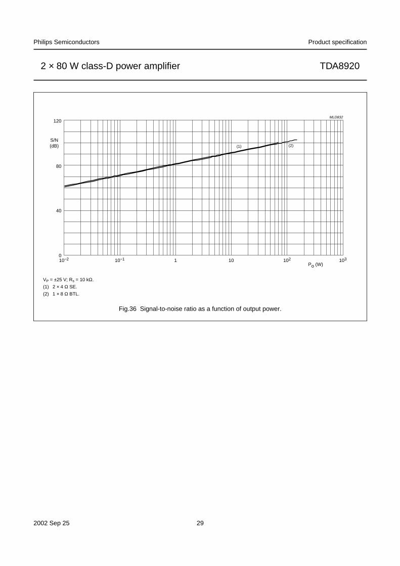
Fig.36 Signal-to-noise ratio as a function of output power.
VP = ±25 V; Rs = 10 kΩ.
(1) 2 × 4 Ω SE.
(2) 1 × 8 Ω BTL.

2002S
ep25
30
Philips S
emiconductors
Product specification
2×
80W
class-D pow
er amplifier
TD
A8920
This text is here in white to force landscape pages to be rotated correctly when browsing through the pdf in the Acrobat reader.This text is here in_white to force landscape pages to be rotated correctly when browsing through the pdf in the Acrobat reader.This text is here inThis text is here inwhite to force landscape pages to be rotated correctly when browsing through the pdf in the Acrobat reader. white to force landscape pages to be ...
handbook, full pagewidth
OUT1
VSSP1
VDDP2
DRIVERHIGH
MBL464
OUT2
BOOT2
TDA8920TH
BOOT1
DRIVERLOW
RELEASE1
SWITCH1
ENABLE1
CONTROLAND
HANDSHAKE
PWMMODULATOR
RFB
RFB
MANAGEROSCILLATORTEMPERATURE SENSORCURRENT PROTECTION
STABI
MODE
ROSC
VSSA
Vmode
COSC
INPUTSTAGE
mute
9
8
IN1−
IN1+
22
21
2017
16
15
VSSP2VSSP1
DRIVERHIGH
DRIVERLOW
RELEASE2
SWITCH2
ENABLE2
CONTROLAND
HANDSHAKEPWMMODULATOR
11SGND1
7OSC
2SGND2
SGND
SGND
6MODE
INPUTSTAGE
mute
5
4IN2−
IN2+
Vin2
Vin1
1924
VSSD
VSSAVSSP
0 V
VSSA
−25 V
VDDPVDDA
+25 V
HW
1
VSSA2
VSSA
12
VSSA1
3
VDDA2
VDDA
10
VDDA1
231318 14
VDDP2PROTSTABI
VDDP1
SGND
Fig.37 Typical application schematic of TDA8920TH.

2002 Sep 25 31
Philips Semiconductors Product specification
2 × 80 W class-D power amplifier TDA8920
17 PACKAGE OUTLINE
UNIT A4(1)
REFERENCESOUTLINEVERSION
EUROPEANPROJECTION ISSUE DATE
02-01-30
IEC JEDEC JEITA
mm+0.08−0.043.5 0.35
DIMENSIONS (mm are the original dimensions)
Notes
1. Limits per individual lead.
2. Plastic or metal protrusions of 0.25 mm maximum per side are not included.
SOT566-3
0 5 10 mm
scale
HSOP24: plastic, heatsink small outline package; 24 leads; low stand-off height SOT566-3
Amax.
detail X
A2
3.53.2
D2
1.10.9
HE
14.513.9
Lp
1.10.8
Q
1.71.5
2.72.2
v
0.25
w
0.25
y Z
8°0°
θ
0.07
x
0.03
D1
13.012.6
E1
6.25.8
E2
2.92.5
bp c
0.320.23
e
1
D(2)
16.015.8
E(2)
11.110.9
0.530.40
A3
A4
A2(A3)
Lpθ
A
Q
D
y
x
HE
E
c
v M A
X
A
bpw MZ
D1D2
E2
E1
e
24 13
1 12
pin 1 index

2002 Sep 25 32
Philips Semiconductors Product specification
2 × 80 W class-D power amplifier TDA8920
18 SOLDERING
18.1 Introduction to soldering surface mountpackages
This text gives a very brief insight to a complex technology.A more in-depth account of soldering ICs can be found inour “Data Handbook IC26; Integrated Circuit Packages”(document order number 9398 652 90011).
There is no soldering method that is ideal for all surfacemount IC packages. Wave soldering can still be used forcertain surface mount ICs, but it is not suitable for fine pitchSMDs. In these situations reflow soldering isrecommended.
18.2 Reflow soldering
Reflow soldering requires solder paste (a suspension offine solder particles, flux and binding agent) to be appliedto the printed-circuit board by screen printing, stencilling orpressure-syringe dispensing before package placement.
Several methods exist for reflowing; for example,convection or convection/infrared heating in a conveyortype oven. Throughput times (preheating, soldering andcooling) vary between 100 and 200 seconds dependingon heating method.
Typical reflow peak temperatures range from215 to 250 °C. The top-surface temperature of thepackages should preferable be kept below 220 °C forthick/large packages, and below 235 °C for small/thinpackages.
18.3 Wave soldering
Conventional single wave soldering is not recommendedfor surface mount devices (SMDs) or printed-circuit boardswith a high component density, as solder bridging andnon-wetting can present major problems.
To overcome these problems the double-wave solderingmethod was specifically developed.
If wave soldering is used the following conditions must beobserved for optimal results:
• Use a double-wave soldering method comprising aturbulent wave with high upward pressure followed by asmooth laminar wave.
• For packages with leads on two sides and a pitch (e):
– larger than or equal to 1.27 mm, the footprintlongitudinal axis is preferred to be parallel to thetransport direction of the printed-circuit board;
– smaller than 1.27 mm, the footprint longitudinal axismust be parallel to the transport direction of theprinted-circuit board.
The footprint must incorporate solder thieves at thedownstream end.
• For packages with leads on four sides, the footprint mustbe placed at a 45° angle to the transport direction of theprinted-circuit board. The footprint must incorporatesolder thieves downstream and at the side corners.
During placement and before soldering, the package mustbe fixed with a droplet of adhesive. The adhesive can beapplied by screen printing, pin transfer or syringedispensing. The package can be soldered after theadhesive is cured.
Typical dwell time is 4 seconds at 250 °C.A mildly-activated flux will eliminate the need for removalof corrosive residues in most applications.
18.4 Manual soldering
Fix the component by first soldering twodiagonally-opposite end leads. Use a low voltage (24 V orless) soldering iron applied to the flat part of the lead.Contact time must be limited to 10 seconds at up to300 °C.
When using a dedicated tool, all other leads can besoldered in one operation within 2 to 5 seconds between270 and 320 °C.

2002 Sep 25 33
Philips Semiconductors Product specification
2 × 80 W class-D power amplifier TDA8920
18.5 Suitability of surface mount IC packages for wave and reflow soldering methods
Notes
1. For more detailed information on the BGA packages refer to the “(LF)BGA Application Note” (AN01026); order a copyfrom your Philips Semiconductors sales office.
2. All surface mount (SMD) packages are moisture sensitive. Depending upon the moisture content, the maximumtemperature (with respect to time) and body size of the package, there is a risk that internal or external packagecracks may occur due to vaporization of the moisture in them (the so called popcorn effect). For details, refer to theDrypack information in the “Data Handbook IC26; Integrated Circuit Packages; Section: Packing Methods”.
3. These packages are not suitable for wave soldering. On versions with the heatsink on the bottom side, the soldercannot penetrate between the printed-circuit board and the heatsink. On versions with the heatsink on the top side,the solder might be deposited on the heatsink surface.
4. If wave soldering is considered, then the package must be placed at a 45° angle to the solder wave direction.The package footprint must incorporate solder thieves downstream and at the side corners.
5. Wave soldering is suitable for LQFP, TQFP and QFP packages with a pitch (e) larger than 0.8 mm; it is definitely notsuitable for packages with a pitch (e) equal to or smaller than 0.65 mm.
6. Wave soldering is suitable for SSOP and TSSOP packages with a pitch (e) equal to or larger than 0.65 mm; it isdefinitely not suitable for packages with a pitch (e) equal to or smaller than 0.5 mm.
PACKAGE (1)SOLDERING METHOD
WAVE REFLOW (2)
BGA, LBGA, LFBGA, SQFP, TFBGA, VFBGA not suitable suitable
HBCC, HBGA, HLQFP, HSQFP, HSOP, HTQFP, HTSSOP, HVQFN,HVSON, SMS
not suitable(3) suitable
PLCC(4), SO, SOJ suitable suitable
LQFP, QFP, TQFP not recommended(4)(5) suitable
SSOP, TSSOP, VSO not recommended(6) suitable

2002 Sep 25 34
Philips Semiconductors Product specification
2 × 80 W class-D power amplifier TDA8920
19 DATA SHEET STATUS
Notes
1. Please consult the most recently issued data sheet before initiating or completing a design.
2. The product status of the device(s) described in this data sheet may have changed since this data sheet waspublished. The latest information is available on the Internet at URL http://www.semiconductors.philips.com.
DATA SHEET STATUS (1) PRODUCTSTATUS(2) DEFINITIONS
Objective data Development This data sheet contains data from the objective specification for productdevelopment. Philips Semiconductors reserves the right to change thespecification in any manner without notice.
Preliminary data Qualification This data sheet contains data from the preliminary specification.Supplementary data will be published at a later date. PhilipsSemiconductors reserves the right to change the specification withoutnotice, in order to improve the design and supply the best possibleproduct.
Product data Production This data sheet contains data from the product specification. PhilipsSemiconductors reserves the right to make changes at any time in orderto improve the design, manufacturing and supply. Changes will becommunicated according to the Customer Product/Process ChangeNotification (CPCN) procedure SNW-SQ-650A.
20 DEFINITIONS
Short-form specification The data in a short-formspecification is extracted from a full data sheet with thesame type number and title. For detailed information seethe relevant data sheet or data handbook.
Limiting values definition Limiting values given are inaccordance with the Absolute Maximum Rating System(IEC 60134). Stress above one or more of the limitingvalues may cause permanent damage to the device.These are stress ratings only and operation of the deviceat these or at any other conditions above those given in theCharacteristics sections of the specification is not implied.Exposure to limiting values for extended periods mayaffect device reliability.
Application information Applications that aredescribed herein for any of these products are forillustrative purposes only. Philips Semiconductors makeno representation or warranty that such applications will besuitable for the specified use without further testing ormodification.
21 DISCLAIMERS
Life support applications These products are notdesigned for use in life support appliances, devices, orsystems where malfunction of these products canreasonably be expected to result in personal injury. PhilipsSemiconductors customers using or selling these productsfor use in such applications do so at their own risk andagree to fully indemnify Philips Semiconductors for anydamages resulting from such application.
Right to make changes Philips Semiconductorsreserves the right to make changes, without notice, in theproducts, including circuits, standard cells, and/orsoftware, described or contained herein in order toimprove design and/or performance. PhilipsSemiconductors assumes no responsibility or liability forthe use of any of these products, conveys no licence or titleunder any patent, copyright, or mask work right to theseproducts, and makes no representations or warranties thatthese products are free from patent, copyright, or maskwork right infringement, unless otherwise specified.

2002 Sep 25 35
Philips Semiconductors Product specification
2 × 80 W class-D power amplifier TDA8920
NOTES

© Koninklijke Philips Electronics N.V. 2002 SCA74All rights are reserved. Reproduction in whole or in part is prohibited without the prior written consent of the copyright owner.
The information presented in this document does not form part of any quotation or contract, is believed to be accurate and reliable and may be changedwithout notice. No liability will be accepted by the publisher for any consequence of its use. Publication thereof does not convey nor imply any licenseunder patent- or other industrial or intellectual property rights.
Philips Semiconductors – a worldwide company
Contact information
For additional information please visit http://www.semiconductors.philips.com . Fax: +31 40 27 24825For sales offices addresses send e-mail to: [email protected] .
Printed in The Netherlands 753503/03/pp36 Date of release: 2002 Sep 25 Document order number: 9397 750 10092