Embed Size (px)
Citation preview

1
Tailoring Exchange Couplings in Magnetic Topological Insulator/Antiferromagnet
Heterostructures
Qing Lin He1†*, Xufeng Kou1†, Alexander J. Grutter2†, Gen Yin1†, Lei Pan1, Xiaoyu Che1, Yuxiang
Liu1, Tianxiao Nie1, Bin Zhang3, Steven M. Disseler2, Brian J. Kirby2, William Ratcliff II2, Qiming
Shao1, Koichi Murata1, Xiaodan Zhu1, Guoqiang Yu1, Yabin Fan1, Mohammad Montazeri1, Xiaodong
Han3, Julie A. Borchers2, and Kang L. Wang1*
1Department of Electrical Engineering, University of California, Los Angeles, California 90095, USA.
2NIST Center for Neutron Research, National Institute of Standards and Technology, Gaithersburg, MD
20899-6102, USA.
3Beijing Key Lab of Microstructure and Property of Advanced Materials, Beijing University of
Technology, 100124, Beijing, China
*Correspondence to: [email protected]; [email protected].
These authors contributed to this work equally.
Supplementary Information
(a) Structural characterizations of the AFM/MTI structures
We have carried out detailed structural characterizations, including X-ray diffraction (XRD), X-ray
reflectivity (XRR), neutron diffraction, and high-resolution scanning transmission electron microscopy
(HRSTEM) on our samples.
Tailoring exchange couplings in magnetic topological-insulator/antiferromagnet heterostructures
SUPPLEMENTARY INFORMATIONDOI: 10.1038/NMAT4783
NATURE MATERIALS | www.nature.com/naturematerials 1

2
We begin with a XRD measurements (shown in Fig. S1) on a typical [AFM(4nm)/MTI(7nm)]n=4
superlattice (SL). In addition to the expected GaAs (111) and (222) substrate peaks, we observed a series
of strong diffraction peaks originating in the MTI layers. Specifically, we can index the (003), (006),
(009), (00 15), and (00 18) Cr-doped (Bi,Sb)2Te3 peaks, indicating extremely high crystallographic
quality. On the other hand, peaks associated with interfacial tellurides (CrTe, Cr3Te4, and Cr2Te3) are not
found in the resulting XRD spectrum, as illustrated by the associated powder diffraction files (PDFs).
Crystal symmetry and lattice matching demand that the growth axis of the CrSb layers is (0001).
However, in the PDF of CrSb we can see that the (0001) diffraction peak is forbidden, while the (0002)
and (0004) peaks are present. As expected, we observed clear (0002) and (0004) CrSb peaks and indexed
them correspondingly.
We can also exploit the lower background levels and increased nuclear contrast offered by neutron
diffraction to detect the NiAs-phase CrSb. We observed the CrSb (0002) neutron diffraction peak
displayed in Fig. S9, which confirms the NiAs-phase CrSb in our material system.
We also carried out HRSTEM from the cross-section of our [AFM(4nm)/MTI(7nm)]n=4 SL to
probe the crystalline structure and local interfacial quality, with results shown in Fig. 1a in the main text.
The upper panel of Fig. 1a shows the low-magnification HAADF image of this superlattice. One can
clearly see that the each layer component is well defined even in a large scale, indicating the high
crystalline qualities of both layer components. The lower panel shows the interfacial region in a higher
magnification, in which the crystalline structures of both materials are well distinguished and form their
own independent lattices, confirming high quality epitaxial growth. We have scanned multiple areas of
several different samples and did not observed intermixing or interfacial phases like CrTe, Cr3Te4, or
Cr2Te3, in agreement with the XRD measurements.
2 NATURE MATERIALS | www.nature.com/naturematerials
SUPPLEMENTARY INFORMATION DOI: 10.1038/NMAT4783

3
In addition to probing the local interface quality through HRSTEM, we have characterized the
long-range interfacial roughness through XRR measurements. Where HRSTEM provides a picture of the
intermixing over nanoscale areas, XRR allows the estimation of roughness across the entire sample and
will incorporate both short-range sources of interfacial roughness, such as chemical intermixing, and long
range effects such as thickness drift across the sample, conformal roughness (such as waviness in the
film), and terracing of the MTI layers. We find that even when all of these effects are combined across a
surface area of approximately 2 cm2, the superlattices are extremely flat. For example, Fig. S2a shows
fitted XRR result of a typical (AFM/MTI)n=4 SL, along with the associated scattering length density depth
profile as shown in b. Here the long-range roughness of the interfaces is ~0.8 nm, indicating a high-quality,
well-defined superlattice spanning the entire surface.
However, it is not sufficient to simply demonstrate high-quality interfaces. We must demonstrate
that intermixing and interfacial chemical reactions cannot be responsible for the observed magnetic
properties of the (AFM/MTI)n SLs. Therefore, we have also performed XRR measurements on an
effectivity identical sample which incorporates undoped TI, (Bi,Sb)2Te3. The fitted reflectivity and
resulting scattering length density are shown in Figs. S2c and d. Here, we extract a slightly larger
interfacial roughness of ~1.5 nm – higher than the (AFM/MTI)n=4 SL but still indicative of a well-defined,
high-quality superlattice. It is unlikely that the increased roughness is due to a change in sample uniformity
between samples, but it may indicate slightly different chemical intermixing or conformal roughness.
Critically, however, the (AFM/undoped TI)n=4 SL does not exhibit the unusual magnetic properties of the
(AFM/MTI)n=4 SL, strongly suggesting that our observations cannot be accounted for by intermixing or
the formation of intermixing tellurides at the interface.
(b) Magneto-transport signature of exchange bias effect
NATURE MATERIALS | www.nature.com/naturematerials 3
SUPPLEMENTARY INFORMATIONDOI: 10.1038/NMAT4783

4
Since the composition of the MTI layers are carefully adjusted such that the Fermi level is right at
the bulk band gap, the transport in the MTIs should be dominated by the surface states, which becomes
massive Dirac fermion under magnetization.
To present a comprehensive study on our material system, we have carried out the magneto-transport
experiments on some typical samples at 1.9 K with results summarized in Fig. S5. Figure S5 shows the
anomalous Hall resistance of an AFM(7nm)/MTI(7nm) heterostructure under zero-field- and ±3T-cooled
processes from 300 K to 1.9 K. We observed that a +3T-cooled process shifts the anomalous Hall signals
to the negative field direction by about 3.9 mT while a -3T-cooled process shifts to the positive field
direction by about 8.2 mT, which is reasonably consistent with the exchange bias effect probed by the
SQUID (Fig. 1c in the main text). Interestingly, we also found that after field-cooled process, the shape
of the anomalous Hall resistance evolves from a symmetric square-shape (zero-field cooled) to
asymmetric, as shown in the inset of Fig. S5a. Such an asymmetric square-shaped anomalous Hall
resistance may stem from the multi-channels in the MTI layer, i.e. both the surface and the bulk,
accompanied with the contributions from the adjacent AFM layer. We cannot observe signature of
exchange bias effect from the anomalous Hall resistance of the [AFM(4nm)/MTI(7nm)]n=4 SL as shown
in Fig. S5b. This is consistent with the SQUID measurements as shown in Fig. 1d and Fig. 2 in the main
text.
We have also compared the magneto-transport results among an isolated MTI layer (Fig. S11), the
AFM(7nm)/MTI(7nm) heterostructure (Fig. S5), and an AFM(4nm)/MTI(7nm)/AFM(4nm) trilayer (Fig.
S3), and the [AFM(4nm)/MTI(7nm)]n=4 SL (Fig. S5). We found that significant exchange bias effect can
only be observed in the AFM/MTI heterostructure but not in an isolated MTI layer, AFM/MTI/AFM
trilayer, or the (AFM/MTI)n SL. These results are consistent with those from the SQUID measurements
4 NATURE MATERIALS | www.nature.com/naturematerials
SUPPLEMENTARY INFORMATION DOI: 10.1038/NMAT4783

5
(Figs. 1d, g, and Fig. 2), which highlight the different roles played by the interfacial exchange coupling
and effective long-range exchange coupling.
(c) Micromagnetic simulations
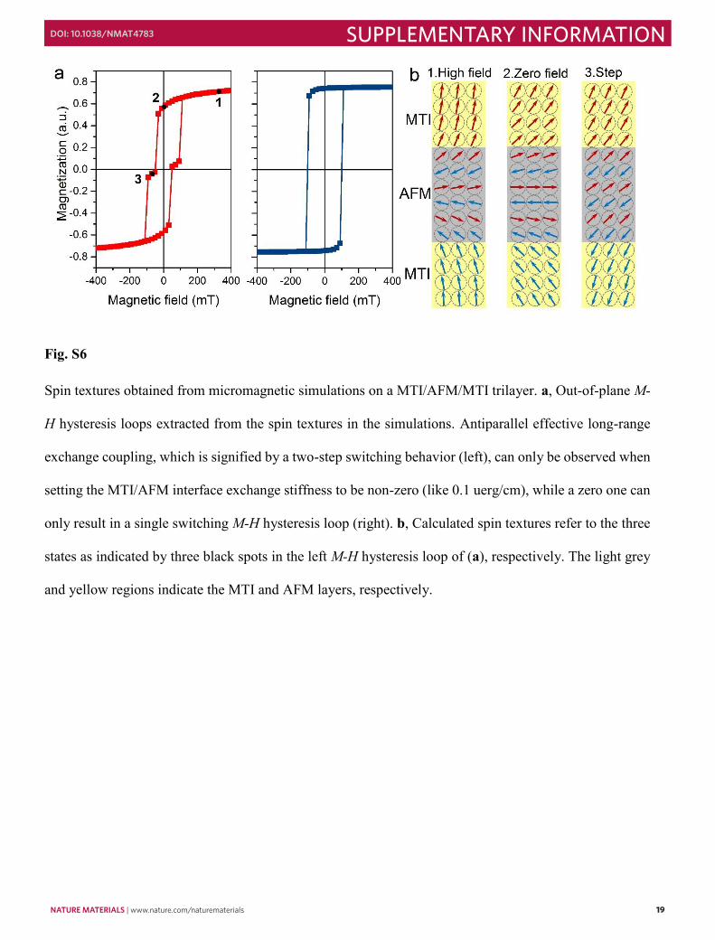
To further specify the possible spin textures in both the AFM CrSb and the MTI Crx(Bi,Sb)2-xTe3 in
the trilayer and SL structures, micromagnetic simulations were carried out using the LLG Micromagnetics
Simulator on a Crx(Bi,Sb)2-xTe3/CrSb/Crx(Bi,Sb)2-xTe3 trilayer. The magnetic energies considered in this
model are the Zeeman energy, interfacial and internal exchange energies, dipole energy and anisotropy
energy. Specifically, the effective long-range exchange coupling was modeled by setting the exchange
stiffness at the MTI/AFM interface to be non-zero, while setting the exchange stiffness between sublayers
within CrSb to be negative to respect the neutron diffraction measurement results. Within the AFM, two
sets of interleaving sublayers essentially represented the two sublattices of CrSb, which are
antiferromagnetically coupled. The material magnetic parameters used in the simulation are estimated as
followed: magnetic stiffnesses: AMTI = 0.2 μerg/cm, AAFM = -0.3 μerg/cm, and AIEC = 0.1 μerg/cm,
estimated from Curie, Néel temperatures, and the exchange field.
To compare simulation outputs with experimental data, an M-H hysteresis loop was extracted from
the simulation data, which is shown in Fig. S6a. As shown in this figure, the extracted M-H hysteresis
loop is reasonably consistent to the major features of the measured M-H hysteresis loop as shown in Fig.
1g, both of which exhibit similar double-step switching behaviors. Specific spin textures of both the MTI
and the AFM layers, as shown in Fig. S6b, are found to be significantly modified from their bulk magnetic
structures (particularly the AFM one) in the trilayer. Such spin textures agree well with the PNR and
neutron diffraction observations of a ferromagnetic- or ferrimagentic- like in-plane magnetization with a
dominant out-of-plane antiferromagnetic spin alignment of the AFM layer. The magnetic spins in MTI
NATURE MATERIALS | www.nature.com/naturematerials 5
SUPPLEMENTARY INFORMATIONDOI: 10.1038/NMAT4783
6
layers near the interfacial regions are found to be canted to lower the interfacial energy. Besides, the
resulting spin texture throughout the whole structure also clearly revealed a Néel-type magnetic domain
wall formed within the AFM layer. It is worth mentioning that setting the MTI/AFM interface exchange
stiffness to be zero results in an absence of the plateau steps in the M-H hysteresis loop, i.e. a single step
switching behavior, which agrees with experimental result when the antiparallel effective long-range
exchange coupling was taken over by a single switching as shown in Fig. 1h.
These simulations assume atomically flat interfaces, highly uniform layer thicknesses, and the growth
of complete CrSb unit cells – all assumptions achievable through molecular beam epitaxy and supported
by the fitting of the neutron reflectivity. The growth of fractional CrSb unit cells or significant thickness
nonuniformity is expected to inhibit the observed antiparallel coupling.
In addition, domain wall width is theoretically proportional to (A/K)1/2, where A and K are exchange
stiffness and anisotropy coefficient, respectively. Therefore, the Néel-type magnetic domain wall may not
be essential as such a spin configuration is strongly dependent on the relative magnitudes of both A and K
of the CrSb.
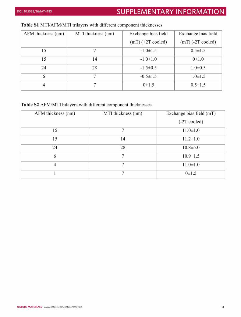
(d) Magnetic interactions from the perspective of thickness dependences in tri- and bi-layer systems
In the trilayer system, the missing exchange bias and the double switching behavior occur only
when the two AFM surfaces coincide with different AFM sublattices. Specifically speaking, as the two
sublattices of the CrSb AFM spins are arranged layer by layer, when the arrangement is A(BA)n, the top
and the bottom MTI layers experience the same spin. In this case, exchange bias is expected to occur. On
the other hand, when the AFM order is AB(AB)n, the two MTI layers experience an opposite interfacial
exchange coupling, thus leading to the double-switching behavior with a minimized exchange bias. In
most (~70%) MTI/AFM/MTI trilayer samples with various thicknesses, we observed the double-
6 NATURE MATERIALS | www.nature.com/naturematerials
SUPPLEMENTARY INFORMATION DOI: 10.1038/NMAT4783

7
switching behavior, and the exchange bias vanishes as expected in the AB(AB)n case. We have
investigated a series of typical MTI/AFM/MTI trilayer samples with different AFM and MTI thickness,
as summarized in Table S1.
In the bilayer system, we observed a significant exchange bias effect as shown in the main text.
Thickness variation was also investigated for the MTI/AFM bilayers and the results are shown in Table
S2. Comparing the tri-layer and bi-layer results, it is clear that the exchange bias in these tri-layer samples
is roughly one order of magnitude smaller than that in the bi-layers, indicating the AB(AB)n type sublattice
is the dominant configuration at the interfaces in these samples.
(e) Dirac fermion spectrum in the (AFM/MTI)n superlattice
The modification of the Dirac fermion spectrum in the (AFM/MTI)n superlattice is mainly induced
by the Cr dopants through a spin-texture modulation due to the interfacial exchange coupling at the
AFM/MTI interface. There are two contributions to the time-reversal-symmetry breaking exchange
coupling: (i) the on-site Hund’s-rule coupling given by the Cr dopants and (ii) the Heisenberg-type
interfacial exchange at the AFM/MTI interface. The Hund’s-rule coupling is between atomic orbitals on
the same site, which is usually at the level of ~eV, while the interfacial Heisenberg exchange is mainly
induced by the nearest-neighbor wave function overlap. Since the wave functions exponentially decay at
the interfaces, the Heisenberg exchange (~meV) is usually orders of magnitude smaller than the on-site
Hund’s rule coupling. Thus, the Hund’s rule coupling given by the Cr dopants dominates the spectrum of
the MTI surface states.
Equally important, it is noted that the magnetization of the doped Cr atoms would tilt when the MTI
layer is adjacent to the AFM layer; in other words, the exchange gap in the MTI layer is also modulated
by the AFM layer indirectly. As shown in Fig. 1f and Fig. S6b, the Néel vectors of the CrSb layer are
NATURE MATERIALS | www.nature.com/naturematerials 7
SUPPLEMENTARY INFORMATIONDOI: 10.1038/NMAT4783

8
canted to in-plane, while the Cr dopants on the TI side are out-of-plane, aligned with the external field. At
the interface, the Cr spins tilt to the in-plane direction, hence reducing the perpendicular magnetic moment
as well as the exchange gap. Under such circumstances, it is expected to have a smaller anomalous Hall
signal in the AFM/MTI structure as compared with the pure MTI case. Indeed, in our experiments, by
replacing the AFM layers with MTI, the anomalous Hall resistance is found to increase by ~25%, as shown
in Fig. S11c.
(f) Alternative models for fitting the PNR data
One of the most common challenges to the understanding and interpretation of PNR measurements
is the existence of multiple scattering length density profiles which describe the data equally well. In fact,
cases in which only a single unique model fits the data within the measured Q-range are extremely rare.
It is therefore critical to compare multiple fitted models to understand what conclusions may confidently
be drawn from the measurements. To that end, we have attempted to fit the PNR data using a wide variety
of models, and present several below.
First, we optimized the model presented in the main text, which assumes a ferromagnetic moment in
the Cr-doped (Bi,Sb)2Te3 layers as well as the CrSb layers. Additionally, the interfacial magnetization was
allowed to vary independently from either of the two constituent layers. This model resulted in the best
overall fit as shown in Fig. 3(a) in the main text. However, a reasonable fit was also achieved using a
model in which the magnetism within the CrSb was fit as three magnetically independent layers while the
magnetization of the Cr-doped (Bi,Sb)2Te3 at the interfaces was also allowed to vary separately from the
bulk, as shown in Figs. S7g-i. Such a model allows for the possibility of a more complex Néel-type
magnetic domain wall configuration within the CrSb layers. Because the magnetization in the CrSb layer
may vary over extremely short length scales in this model, it is expected that, as long as the average net
8 NATURE MATERIALS | www.nature.com/naturematerials
SUPPLEMENTARY INFORMATION DOI: 10.1038/NMAT4783
9
in-plane magnetization within the CrSb layer remains similar, this fit will agree well with the one
presented in the main text throughout the measured Q-range. Thus, it is not surprising that such optimized
model as shown in Figs. S7g-i yields a very similar fit to the one presented in the main text, suggesting
that more complex spin structures within the CrSb cannot be excluded. Although the best fit is achieved
with a complex, oscillatory magnetization depth profile within the CrSb layers, several other CrSb spin
structures are also supportive. These alternative structures include a uniform magnetization in the CrSb
layers, or magnetized CrSb interfaces and purely antiferromagnetic CrSb in the center of the layer. Despite
the variety of possible spin structures supported by the PNR, all models which describe the data are highly
sensitive to the average magnetization in Crx(Bi,Sb)2-xTe3 (40-41 emu/cm3) and CrSb (61-63 emu/cm3)
layers. Although PNR modeling often results in multiple models which well describe the data, in this case
we may explicitly exclude several competing models which provided significantly worse fits to the
observed reflectivity.
In contrast, models in which the magnetization is confined exclusively to the Cr-doped (Bi,Sb)2Te3
layers, shown in Figs. S7a-c, or the CrSb layers, in Figs. S7d-f, clearly fail to describe the measured
reflectometry. For example, in Fig. S7c, we can see that the spin asymmetry is much too large from 0.6-
1.3 nm-1. Furthermore, the spin-splitting is the wrong sign at the second order SL reflection. Similarly, the
model incorporating nonmagnetic (Bi,Sb)2Te3 layers fails quite badly throughout the entire Q-range as
shown in Fig. S7f, with incorrect signal magnitude at both SL peaks as well as insufficient spin splitting
near the critical edge.
All presented models have been optimized within the imposed constraints using the NIST Refl1d
software package29. Fitted thicknesses agree reasonably well with those of the designed SL. For example,
the nominal thickness of each CrSb layer in the SL is 30 Å, while the fitted thickness was 25 Å. It should
additionally be noted that the expected nuclear scattering length densities of Cr-doped (Bi,Sb)2Te3 and
NATURE MATERIALS | www.nature.com/naturematerials 9
SUPPLEMENTARY INFORMATIONDOI: 10.1038/NMAT4783
10
CrSb are nearly identical, and that the majority of the contrast between layers originates in the changing
magnetic scattering length density. Therefore, the model optimization is far more sensitive to the
magnetization and magnetic layer thicknesses, rather than the structural thicknesses. For the model
presented in the main text, we find in-plane magnetizations of approximately 40 emu/cc in the Cr-doped
(Bi,Sb)2Te3 and 63 emu/cc in the CrSb for an in-plane applied field of 700 mT. In summary, the PNR
measurements clearly indicate a spontaneous net magnetization in both the Cr-doped (Bi,Sb)2Te3 and
CrSb layers. Within the CrSb layers, both a simple model with constant magnetization and a more complex
Néel-type magnetic domain wall configuration describe the data equally well.
For the AFM/MTI/AFM trilayer case, a similar approach was also utilized to confirm the magnetic
ordering in the AFM layers. The model used in main text is constructed based on two minimally
magnetized AFM (5 emu/cc or less) and a magnetized MTI layer, which well describes the PNR data. On
the other hand, models with both magnetized AFMs and a magnetized MTI layer were also used to fit the
data (Fig. S8a-c). However, even after parameter optimization such a model clearly fails to describe the
PNR spectra of the trilayer (particularly in the regions of 0.25-0.5 and 1.0-1.25 nm-1), supporting the
conclusion that the magnetization is confined exclusively within the MTI layer. We further measured the
PNR spectra at 150 K and 265 K, above the TC of the MTI but below the AFM Neel temperature, as shown
in Fig. S8d. These measurements show no net magnetization within any layer of the trilayer structure,
demonstrating that the magnetic susceptibility of the AFM layers is small enough to be completely
neglected and further supporting the assertion that the AFM layers are nonmagnetic in this geometry.
(g) Spontaneous magnetization due to interfacial exchange couplings
The interfacial exchange coupling between CrSb and Crx(Bi,Sb)2-xTe3 in SLs is reflected by the initial
magnetization processes in both longitudinal resistance (Rxx) and Hall resistance (Rxy) measurements.
After ZFC the samples from 300 K to 1.9 K, a perpendicular magnetic field is swept from zero to 3 T for
10 NATURE MATERIALS | www.nature.com/naturematerials
SUPPLEMENTARY INFORMATION DOI: 10.1038/NMAT4783

11
an initial magnetization, followed by a major hysteresis loop measurement via cycling the field between
3 T and −3 T. As shown in Fig. S11, the resulting butterfly-like Rxx and square-shaped Rxy mainly come
from the contribution of the Crx(Bi,Sb)2-xTe3 layers, which is illustrated by negligible hysteresis behaviors
of Rxx and Rxy in two control samples, a CrSb (12 nm)/(Bi,Sb)2Te3 (2 nm) bilayer and a [CrSb (4
nm)/(Bi,Sb)2Te3 (7 nm)]n=4 SL. Here, in the CrSb (12 nm)/(Bi,Sb)2Te3 (2 nm) bilayer, the thin (Bi,Sb)2Te3
acts as a buffer layer that provides for the epi-growth of CrSb layer.
Taking the [CrSb/Cr0.16(Bi,Sb)1.84Te3]n=4 SL as an example, the initial magnetization curve of Rxx
(light red curve, Fig. S11b) shows a peak located at a field slightly higher than that in the major loop (red
curve, Fig. S11b), while the corresponding initial magnetization curve of Rxy (light red curve, Fig. S11c)
nearly overlaps with the square-shaped major loop (red curve, Fig. S11c). As these magnetizing features
are obtained after a ZFC process, they are considered a signature of spontaneous magnetization. This is
consistent with the conclusion from PNR of a spontaneous net magnetization in the Cr-doped (Bi,Sb)2Te3
layers. In contrast, in a single MTI layer, the initial magnetization curves in Rxx (light blue curve, Fig.
S11b) starts from a higher resistance state, while the corresponding Rxy initial magnetization curve (light
blue curve, Fig. S11c) deviates from the major loop (blue curve, Fig. S11c) until a ~150 mT field is
applied. These features reveals a multi-domain state in a single MTI layer after ZFC process. To
quantitatively characterize such a spontaneous magnetization behavior, a magnon magnetoresistance
(RMMR) model30, which is widely used to describe a partial magnetization state, is adopted to calculate the
ratio of spontaneous magnetization to the saturated magnetization:
𝑅𝑅𝑀𝑀𝑀𝑀𝑀𝑀 = 𝛼𝛼 𝑀𝑀𝑀𝑀𝑆𝑆
𝐵𝐵
where M is the magnetization along the magnetic anisotropy axis (out-of-plane), MS is the saturated
magnetization, B is the external magnetic field along the magnetic anisotropy axis and 𝛼𝛼 = (𝜕𝜕𝑀𝑀𝜕𝜕𝜕𝜕)𝑠𝑠𝑠𝑠𝑠𝑠 is the
slope of RMMR(B) extracted from a saturated magnetization state as shown in Fig. S11b. Thus, the slope
NATURE MATERIALS | www.nature.com/naturematerials 11
SUPPLEMENTARY INFORMATIONDOI: 10.1038/NMAT4783

12
of the initial magnetization curve is referred to 𝛼𝛼 𝑀𝑀𝑀𝑀𝑆𝑆
during the initial magnetization process. We then
obtained α ~ 3.04 according to the major Rxx loop. This results in an estimated value of M/MS ~ 0.908
using the slope in initial magnetization curve, which reveals that 90.8% magnetization is spontaneously
established after ZFC from 300 K to 1.9 K in the SL.
Considering that the Néel temperature of CrSb is much higher than the TC of Crx(Bi,Sb)2-xTe3, such
a spontaneous magnetization behavior in Crx(Bi,Sb)2-xTe3 is believed to stem from an induced FM
ordering arisen from the CrSb/Crx(Bi,Sb)2-xTe3 interfaces. While cooling from room temperature to 1.9
K, at the interfacial regions, spins in Crx(Bi,Sb)2-xTe3 start to couple to the adjacent antiferromagnetic
spins in AFM. This results in a spontaneous predetermination of spin direction in the FM to that of the
AFM. In contrast, such a spontaneous magnetization is barely observable in a single layer of
Cr0.16(Bi,Sb)1.84Te3 layer as the corresponding Rxx and Rxy do not exhibit a clear hysteresis signature until
the sample is fully magnetized under a large external field (e.g. 3 T). The above observations clearly
demonstrate that interfacial exchange interaction between Crx(Bi,Sb)2-xTe3 and CrSb results in a strong
spontaneous magnetization in the absence of an external field31.
12 NATURE MATERIALS | www.nature.com/naturematerials
SUPPLEMENTARY INFORMATION DOI: 10.1038/NMAT4783
13
Table S1 MTI/AFM/MTI trilayers with different component thicknesses
AFM thickness (nm) MTI thickness (nm) Exchange bias field
(mT) (+2T cooled)
Exchange bias field
(mT) (-2T cooled)
15 7 -1.0±1.5 0.5±1.5
15 14 -1.0±1.0 0±1.0
24 28 -1.5±0.5 1.0±0.5
6 7 -0.5±1.5 1.0±1.5
4 7 0±1.5 0.5±1.5
Table S2 AFM/MTI bilayers with different component thicknesses
AFM thickness (nm) MTI thickness (nm) Exchange bias field (mT)
(-2T cooled)
15 7 11.0±1.0
15 14 11.2±1.0
24 28 10.8±5.0
6 7 10.9±1.5
4 7 11.0±1.0
1 7 0±1.5
NATURE MATERIALS | www.nature.com/naturematerials 13
SUPPLEMENTARY INFORMATIONDOI: 10.1038/NMAT4783

14
Fig. S1
a, XRD pattern obtained from an [AFM(4nm)/MTI(7nm)]n=4 superlattice. b-e, Standard XRD powder
pattern files (PDFs) of CrSb, CrTe, Cr3Te4, and Cr2Te3, respectively.
14 NATURE MATERIALS | www.nature.com/naturematerials
SUPPLEMENTARY INFORMATION DOI: 10.1038/NMAT4783

15
Fig. S2
X-ray reflectivity data obtained from a, an (AFM/MTI)n=4 superlattice and b, the corresponding depth
profiles of real/complex scattering length densities, which best fitted the XRR data. c and d, presenting
the corresponding content for an (TI/MTI)n=4 superlattice.
NATURE MATERIALS | www.nature.com/naturematerials 15
SUPPLEMENTARY INFORMATIONDOI: 10.1038/NMAT4783

16
Fig. S3
Hall resistance measurements on three AFM/MTI/AFM trilayers. All the AFM layers are fixed to be 4 nm
thick while the intervening MTI thickness is decreased from 21 nm to 14 nm and 7 nm in order to
investigate the origin of the proximity-induced magnetic ordering enhancement. The magnetic ordering
enhancement can be reflected by HC of the Hall resistance, which is found to increase along with the
decrease of the MTI thickness. Such a dependence indicates that the enhancement is dominated by the
interface between the MTI and the AFM layers, implying the important role played by the surface Dirac
fermion from the MTI.
16 NATURE MATERIALS | www.nature.com/naturematerials
SUPPLEMENTARY INFORMATION DOI: 10.1038/NMAT4783

17
Fig. S4
a-e, Exchange bias effect and vertical shifts in M-H loops obtained from an AFM/MTI bilayer at different
temperatures. An out-of-plane magnetic field of ± 1.5 T is used in the field-cooled process. f, A summary
of temperature-dependent-exchange bias field.
NATURE MATERIALS | www.nature.com/naturematerials 17
SUPPLEMENTARY INFORMATIONDOI: 10.1038/NMAT4783

18
Fig. S5 Anomalous Hall resistance measurements obtained from a, an AFM(7nm)/MTI(7nm)
heterostructure and b, an [AFM(4nm)/MTI(7nm)]n=4 SL after zero-field cooled and ±3T cooled processes.
The insets show the low field region of the main panels in finer scales with arrows showing the exchange
bias fields; however, the exchange bias effect is vanishing in the SL. These results are consistent with the
SQUID measurements in Figs. 1 and 2 of the main text.
18 NATURE MATERIALS | www.nature.com/naturematerials
SUPPLEMENTARY INFORMATION DOI: 10.1038/NMAT4783
19
Fig. S6
Spin textures obtained from micromagnetic simulations on a MTI/AFM/MTI trilayer. a, Out-of-plane M-
H hysteresis loops extracted from the spin textures in the simulations. Antiparallel effective long-range
exchange coupling, which is signified by a two-step switching behavior (left), can only be observed when
setting the MTI/AFM interface exchange stiffness to be non-zero (like 0.1 uerg/cm), while a zero one can
only result in a single switching M-H hysteresis loop (right). b, Calculated spin textures refer to the three
states as indicated by three black spots in the left M-H hysteresis loop of (a), respectively. The light grey
and yellow regions indicate the MTI and AFM layers, respectively.
NATURE MATERIALS | www.nature.com/naturematerials 19
SUPPLEMENTARY INFORMATIONDOI: 10.1038/NMAT4783

20
Fig. S7
Three alternative different models used to fit the PNR data. For an example, a shows the structural and
magnetic scattering length densities constructed in the model in which the magnetization is confined
exclusively to the MTI layers. b shows the corresponding fitting results to the PNR data in a while c shows
the corresponding fittings result to the spin asymmetries, respectively. Corresponding PNR data and
fittings are shown in d-f, the magnetization is confined exclusively to the AFM layers, and g-i, a more
complex oscillatory spin structures within the AFM. In the former two models, i.e. a and d, the fittings
clearly fail to describe the measured reflectometries, while in the last model, g, a good fitting to the data
is obtained.
20 NATURE MATERIALS | www.nature.com/naturematerials
SUPPLEMENTARY INFORMATION DOI: 10.1038/NMAT4783

21
Fig. S8
A model with a magnetized AFM layer used to fit the PNR data of an AFM/MTI/AFM trilayer. a, PNR
data obtained from such a trilayer along with a fit based on the model demonstrated in (b). b, Structural
and magnetic scattering length densities used in this model, which contains two magnetized AFM and a
magnetized TI layers. c, To carefully check the fitting quality, spin asymmetry of the resulting PNR data
along with the fitting is plotted together. In this model, the fitting clearly fail to describe the measured
reflectometry. d, Spin asymmetry of the AFM/MTI/AFM trilayer measured at 150 K and 265 K, which
statistically shows that the nonmagnetic nature of the AFM layers when the temperature is above TC of
the MTI layer.
NATURE MATERIALS | www.nature.com/naturematerials 21
SUPPLEMENTARY INFORMATIONDOI: 10.1038/NMAT4783

22
Fig. S9
Growth axis (c-axis) polarized neutron diffraction of the (0002) CrSb peak for a
[CrSb/Cr0.16(Bi,Sb)1.84Te3]n=15 SL. Both spin-flip and non spin-flip channels were collected for neutron
polarization (a) in the film plane and (b) along the scattering vector. In both cases, no significant spin-flip
scattering is observed, demonstrating that there is no magnetic contribution to the observed peak.
22 NATURE MATERIALS | www.nature.com/naturematerials
SUPPLEMENTARY INFORMATION DOI: 10.1038/NMAT4783

23
Fig. S10. Arrott plots of Hall resistance
Rxy obtained from various magnetic
structures: a, a MTI single layer, b, an
AFM/MTI bilayer, [AFM/MTI]n SLs
with different period n. c, n=2. d, n=4. e,
n=6. f, n=8. g, n=10.
NATURE MATERIALS | www.nature.com/naturematerials 23
SUPPLEMENTARY INFORMATIONDOI: 10.1038/NMAT4783

24
Fig. S11
Characterization of spontaneous magnetization obtained through magneto-electrical measurements at 1.9
K with schematic shown in a. The resulting the longitudinal (Rxx) and the Hall resistances (Rxy) are shown
in b and c. Four samples are used in the magneto transport measurements: an AFM (12 nm)/ TI (2 nm)
bilayer, and an [AFM (4 nm)/ TI (7 nm)]n=4 SL, a MTI single layer, and an [AFM (4 nm)/ MTI (7 nm)]n=4
SL, as denoted close to the resulting curves. After a ZFC from 300 K to 1.9 K, in the (AFM/MTI)n=4 SL,
the initial magnetization curve of Rxx (light red curve in b) shows a peak located at a field slightly higher
than that in the major loop (red curve in b), while the corresponding initial magnetization curve of Rxy
(light red curve in c) nearly overlaps with the square-shaped major loop (red curve in c), acting a signature
of spontaneous magnetization. This is consistent with the conclusion from PNR of a spontaneous net
magnetization in the MTI layers. In contrast, in a single MTI layer, the initial magnetization curves in Rxx
(light blue curve in b) starts from a higher resistance state that refers to a multi-domain state, while the
corresponding Rxy initial magnetization curve (light blue curve in c) deviates from the major loop (blue
curve in c) until a ~150 mT field is applied.
24 NATURE MATERIALS | www.nature.com/naturematerials
SUPPLEMENTARY INFORMATION DOI: 10.1038/NMAT4783

25
Fig. S12
Major and minor M-H loops of a [CrSb/Cr0.16(Bi,Sb)1.84Te3]n=2 SL obtained at different temperatures using
SQUID.
NATURE MATERIALS | www.nature.com/naturematerials 25
SUPPLEMENTARY INFORMATIONDOI: 10.1038/NMAT4783
26
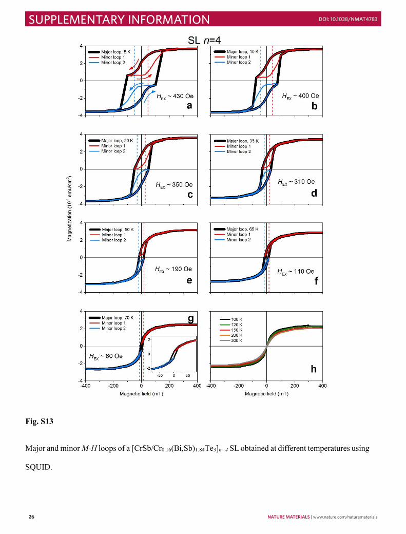
Fig. S13
Major and minor M-H loops of a [CrSb/Cr0.16(Bi,Sb)1.84Te3]n=4 SL obtained at different temperatures using
SQUID.
26 NATURE MATERIALS | www.nature.com/naturematerials
SUPPLEMENTARY INFORMATION DOI: 10.1038/NMAT4783

27
Fig. S14
Major and minor M-H loops of a [CrSb/Cr0.16(Bi,Sb)1.84Te3]n=6 SL obtained at different temperatures using
SQUID.
NATURE MATERIALS | www.nature.com/naturematerials 27
SUPPLEMENTARY INFORMATIONDOI: 10.1038/NMAT4783
28
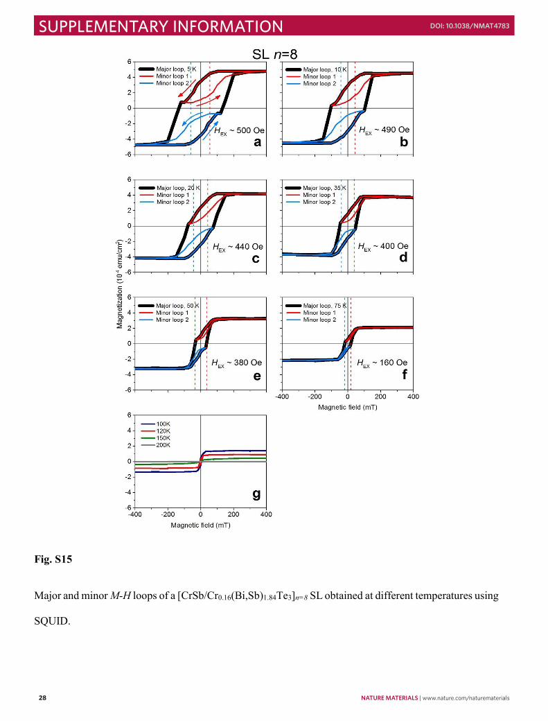
Fig. S15
Major and minor M-H loops of a [CrSb/Cr0.16(Bi,Sb)1.84Te3]n=8 SL obtained at different temperatures using
SQUID.
28 NATURE MATERIALS | www.nature.com/naturematerials
SUPPLEMENTARY INFORMATION DOI: 10.1038/NMAT4783

29
Fig. S16
Major and minor M-H loops of a [CrSb/Cr0.16(Bi,Sb)1.84Te3]n=10 SL obtained at different temperatures
using SQUID.
NATURE MATERIALS | www.nature.com/naturematerials 29
SUPPLEMENTARY INFORMATIONDOI: 10.1038/NMAT4783


![Tailoring Topological Edge States with Photonic Crystal ... · nonlinear parametric generation [13, 14], protection of single photons [15], and entangled photonic states [16, 17]](https://img.dokumen.tips/doc/110x75/5f344616b582d6297a049e94/tailoring-topological-edge-states-with-photonic-crystal-nonlinear-parametric.jpg)