Embed Size (px)
Citation preview
SERVICE MANUAL
No. 82884July 2001
HR-S6850MS/S7850MS/S7851MS/S8850MS
CARACTÉRISTIQUES TECHNIQUES (The specifications shown pertain specifically to the model HR-S8850MS)
MAGNETOSCOPE
Printed in Japan
VICTOR COMPANY OF JAPAN, LIMITEDVIDEO DIVISION S40894
This service manual is printed on 100% recycled paper.COPYRIGHT © 2001 VICTOR COMPANY OF JAPAN, LTD.
HR
-S6850M
S/S
7850MS
/S7851M
S/S
8850MS
No
. 82884
INSERT A.DUB
GÉNÉRALESAlimentation : CA 220 V – 240 V ` , 50 Hz/60 HzConsommation
Alimentation en marche : 22 WAlimentation en veille : 3,8 W
TempératuresFonctionnement : 5°C à 40°CStockage : -20°C à 60°C
Position de fonctionnement : Seulement horizontaleDimensions (LxHxP) : 400 mm x 94 mm x 278 mmPoids : 3,7 kgFormat : Standard S-VHS/VHS PAL/SECAMLargeur de bande : 12,65 mmVitesse de bande
(VN) : 23,39 mm/s(LD) : 11,70 mm/s(EP)* : 7,80 mm/s
Durée maximale d’enregistrement(VN) : 240 mn avec une cassette vidéo E-240(LD) : 480 mn avec une cassette vidéo E-240(EP)* : 720 mn avec une cassette vidéo E-240* Signaux PAL seulement
VIDÉO/AUDIOSystème de signal : Signaux couleur PAL/SECAM et signal
monochrome CCIR, 625 lignes/50 tramesSystème d’enregistrement : Balayage hélicoïdal DA4 (Double Azimuth)Entrée : 0,5 Vcc à 2,0 Vcc, 75 ohms, asymétriqueSortie : 1,0 Vcc, 75 ohms, asymétriqueRapport signal/bruit : 45 dBRésolution horizontale : 400 lignes (S-VHS-PAL, VN/LD)
250 lignes (VHS-PAL, VN/LD)350 lignes (S-VHS-PAL, EP)220 lignes (VHS-PAL, EP)240 lignes (VHS-SECAM, VN/LD)
Gamme de fréquence : 70 Hz à 10.000 Hz (Audio normal)20 Hz à 20.000 Hz (Audio Hi-Fi)
Entrée/sortie : Connecteurs péritélévision à 21 broches:ENTREE/SORTIE x 1, ENTREE/DECODEUR x 1Connecteurs RCA:ENTREE VIDEO x 1, ENTREE AUDIO x 1,SORTIE AUDIO x 1Connecteurs S-Vidéo: ENTREE x 1, SORTIE x 1
SYNTONISEURSystème de syntonisation : Syntoniseur à synthèse de fréquenceCapacité de canaux TV : 99 positions (+ position AUX)Canaux couverts
MINUTERIERéférence de l’horloge : Par quartzCapacité de programmation : Minuterie sur 1 an/8 programmesDurée de soutien mémoire : 10 mn
ACCESSOIRESAccessoires fournis : Câble RF,
Câble péritélévision à 21 broches,Contrôleur satellite,Boîtier de télécommande à infrarouge,Pile “R6” x 2
ATTENTION:Ce magnétoscope contient des microprocesseurs. Des bruits électroniquesexternes ou des interférences peuvent causer un mauvais fonctionnement.Dans de tels cas, couper l’alimentation et débrancher le cordond’alimentation. Puis le rebrancher et remettre l’alimentation. Sortir la cassette.Après contrôle de la cassette, faire fonctionner l’appareil comme d’ordinaire.
Les caractéristiques techniques sont pour le mode VN à moinsd’indication contraire.Présentation et caractéristiques modifiables sans préavis.
GammeSECAM L PAL B/G
Fréquence Canaux Fréquence CanauxVHF 49 MHz – 65 MHz 2 – 4 47 MHz – 89 MHz E2 – E4(LOW) X, Y, Z
E5 – E12VHF 104 MHz 5 – 10 104 MHz S1 – S20(HIGH) – 300 MHz CATV – 300 MHz M1 – M10
U1 – U10Hyper 300 MHz – 470 MHz CATV 302 MHz – 470 MHz S21 – S41UHF 470 MHz – 862 MHz 21 – 69 470 MHz – 862 MHz E21 – E69

3.1.3 Color (colour) bar signal,Color (colour) bar pattern ......... 3-13.1.4 Switch settings and standard precautions ....................... 3-13.1.5 EVR Adjustment .............................................................. 3-1
3.2 Servo circuit .......................................................................... 3-23.2.1 Switching point ................................................................ 3-23.2.2 Slow tracking preset ........................................................ 3-2
3.3 Video circuit .......................................................................... 3-23.3.1 D/A level .......................................................................... 3-23.3.2 EE Y/PB Y (S-VHS/VHS) level ......................................... 3-23.3.3 REC color (colour) level ................................................... 3-33.3.4 Video EQ (Frequency response) ..................................... 3-33.3.5 Auto picture initial setting ................................................. 3-4
3.4 Audio circuit .......................................................................... 3-43.4.1 Audio REC FM................................................................. 3-4
3.5 Syscon circuit ....................................................................... 3-43.5.1 Timer clock ...................................................................... 3-4
3.6 PAL/SECAM Converter circuit .............................................. 3-53.6.1 Colour difference level ..................................................... 3-53.6.2 SECAM burst position ..................................................... 3-5
4. CHARTS AND DIAGRAMSNOTES OF SCHEMATIC DIAGRAM .......................................... 4-1CIRCUIT BOARD NOTES ........................................................... 4-24.1 BOARD INTERCONNECTIONS .......................................... 4-34.2 MAIN (VIDEO/AUDIO) SCHEMATIC DIAGRAM .................. 4-54.3 MAIN (ON SCREEN) SCHEMATIC DIAGRAM .................... 4-74.4 MAIN (SECAM) SCHEMATIC DIAGRAM ............................. 4-94.5 MAIN (SYSCON) SCHEMATIC DIAGRAM ........................ 4-114.6 MAIN (SW.REG) SCHEMATIC DIAGRAM ......................... 4-134.7 MAIN (TUNER) SCHEMATIC DIAGRAM ........................... 4-154.8 MAIN (SW/DISPLAY), MINI FRONT, S-JACK AND ADV. JOG
SCHEMATIC DIAGRAMS ..................................................... 4-174.9 MAIN (MAIN TERMINAL) SCHEMATIC DIAGRAM............ 4-194.10 2D DIGITAL SCHEMATIC DIAGRAM
[HR-S6850MS/S7850MS/S7851MS] ............................... 4-214.11 3D/TBC(2M) SCHEMATIC DIAGRAM [HR-S8850MS] .... 4-234.12 TERMINAL (S-SUB) SCHEMATIC DIAGRAM ................. 4-254.13 TERMINAL (I/O) SCHEMATIC DIAGRAM ....................... 4-274.14 DEMODULATOR SCHEMATIC DIAGRAM ...................... 4-294.15 S-P CONVERTER SCHEMATIC DIAGRAM .................... 4-314.16 MAIN CIRCUIT BOARD................................................... 4-334.17 2D DIGITAL AND 3D DIGITAL/2M CIRCUIT BOARDS ... 4-364.18 TERMINAL CIRCUIT BOARD ......................................... 4-374.19 S-P CONVERTER AND DEMODULATOR CIRCUIT BOARDS 4-384.20 FDP GRID ASSIGNMENT AND ANODE CONNECTION 4-394.21 REMOTE CONTROLLER SCHEMATIC DIAGRAMS ...... 4-404.22 WAVEFORMS .................................................................. 4-414.23 VOLTAGE CHARTS ......................................................... 4-434.24 CPU PIN FUNCTION ....................................................... 4-454.25 SYSTEM CONTROL BLOCK DIAGRAM ......................... 4-474.26 VIDEO BLOCK DIAGRAM ............................................... 4-494.27 AUDIO BLOCK DIAGRAM ............................................... 4-53
5. PARTS LIST5.1 PACKING AND ACCESSORY ASSEMBLY <M1> ............... 5-15.2 FINAL ASSEMBLY <M2> .................................................... 5-25.3 MECHANISM ASSEMBLY <M4> ........................................ 5-45.4 ELECTRICAL PARTS LIST .................................................. 5-6
MAIN BOARD ASSEMBLY <03> ............................................... 5-62D DIGITAL BOARD ASSEMBLY <05>(MODEL:A,B,C) ......... 5-143D DIGITAL/2M BOARD ASSEMBLY <05>(MODEL:D) .......... 5-15TERMINAL BOARD ASSEMBLY <06> ................................... 5-16A/C HEAD BOARD ASSEMBLY <12> ..................................... 5-18DEMOD BOARD ASSEMBLY <14> ........................................ 5-18MINI FRONT BOARD ASSEMBLY(MODEL:B,C,D)<28> ........ 5-19S JACK BOARD ASSEMBLY <36> ......................................... 5-19ADV.JOG BOARD ASSEMBLY <38> ....................................... 5-19LOADING MOTOR BOARD ASSEMBLY <55> ....................... 5-19S/P CONVERTER BOARD ASSEMBLY <87> ........................ 5-19
Important Safety PrecautionsINSTRUCTIONS
1. DISASSEMBLY1.1 Disassembly flow chart ......................................................... 1-11.2 How to read the disassembly and assembly ........................ 1-11.3 Disassembly/assembly method ............................................ 1-11.4 Service position .................................................................... 1-4
1.4.1 How to set the “Service position” ..................................... 1-41.5 Mechanism service mode..................................................... 1-4
1.5.1 How to set the “Mechanism service mode” ..................... 1-41.6 Jig RCU mode ...................................................................... 1-4
1.6.1 Setting the Jig RCU mode ............................................... 1-41.6.2 Setting the User RCU mode ............................................ 1-4
1.7 Servicing items related to video navigation .......................... 1-41.8 Emergency display function .................................................. 1-5
1.8.1 Displaying the EMG information ...................................... 1-51.8.2 Clearing the EMG history ................................................ 1-51.8.3 EMG content description ................................................. 1-61.8.4 EMG detail information <1> ............................................. 1-71.8.5 EMG detail information <2> ............................................. 1-8
2. MECHANISM ADJUSTMENT2.1 Before starting repair and adjustment ................................... 2-1
2.1.1 Precautions ..................................................................... 2-12.1.2 Checking for proper mechanical operations .................... 2-12.1.3 Manually removing the cassette tape .............................. 2-12.1.4 Jigs and tools required for adjustment ............................. 2-22.1.5 Maintenance and inspection ............................................ 2-3
2.2 Replacement of major parts ................................................. 2-62.2.1 Before starting disassembling (Phase matching between
mechanical parts) ............................................................ 2-62.2.2 How to set the “Mechanism assembling mode” ............... 2-62.2.3 Cassette holder assembly ............................................... 2-62.2.4 Pinch roller arm assembly ............................................... 2-82.2.5 Guide arm assembly and press lever assembly .............. 2-82.2.6 A/C head ......................................................................... 2-82.2.7 Loading motor ................................................................. 2-82.2.8 Capstan motor ................................................................. 2-92.2.9 Pole base assembly (supply or take-up side) .................. 2-92.2.10 Rotary encoder ........................................................... 2-102.2.11 Clutch unit ................................................................... 2-102.2.12 Change lever assembly, direct gear, clutch gear and coupling gear 2-102.2.13 Link lever ..................................................................... 2-112.2.14 Cassette gear, control cam and worm gear ................ 2-112.2.15 Control plate ............................................................... 2-112.2.16 Loading arm gear (supply or take-up side) and
loading arm gear shaft .................................................. 2-122.2.17 Take-up lever, take-up head and control plate guide .. 2-132.2.18 Capstan brake assembly ............................................ 2-132.2.19 Sub brake assembly (take-up side) ............................ 2-132.2.20 Main brake assembly (take-up side), reel disk (take-up side)
and main brake assembly (supply side) ............................... 2-132.2.21 Tension brake assembly, reel disk (supply side) and
tension arm assembly ................................................. 2-142.2.22 Idler lever, idler arm assembly .................................... 2-142.2.23 Stator assembly .......................................................... 2-142.2.24 Rotor assembly ........................................................... 2-142.2.25 Upper drum assembly ................................................. 2-15
2.3 Compatibility adjustment .................................................... 2-162.3.1 FM waveform linearity ................................................... 2-162.3.2 Height and tilt of the A/C head ...................................... 2-172.3.3 A/C head phase (X-value) ............................................. 2-172.3.4 Standard tracking preset ............................................... 2-182.3.5 Tension pole position ..................................................... 2-18
3. ELECTRICAL ADJUSTMENT3.1 Precaution ............................................................................ 3-1
3.1.1 Required test equipments ............................................... 3-13.1.2 Required adjustment tools ............................................... 3-1
TABLE OF CONTENTSSection Title Page Section Title Page
HR-S6850MS HR-S7850MS HR-S7851MS HR-S8850MS
FLYING ERASE HEAD NOT USED USED USED USEDDIGITAL 3R/TBC/FRAME MEMORY NOT USED NOT USED NOT USED USEDYNR/CNR/S.COLOR NOT USED / 2D/NOT USED NOT USED / 2D / NOT USED NOT USED / 2D / NOT USED USED (3D) / 3D / USED (3D)RE-TAKE/ASSEMBLE EDIT NOT USED / A.F.E. USED / Z.F.E. USED / Z.F.E. USED / Z.F.E.INSERT/OPERATION, NOT USED USED/BUTTON USED/BUTTON USED/BUTTONAUDIO DUBBING / OPERATIONHiFi LEVEL METER NOT USED USED USED USEDR.PAUSE TERMINAL NOT USED USED USED USEDREAR OUT AUDIO L/R AUDIO L/R & S-OUT AUDIO L/R & S-OUT AUDIO L/R & S-OUTCABLE BOX OR DBS. BOX OR SAT CTL OPTION OPTION OPTION USEDCABLE MOUSE OPTION OPTION OPTION PROVIDEDRCU V13 SMALL 10KEY V13 SMALL 10KEY V13 SMALL 10KEY V13 LCDRCU TYPE / COLOR V14#E11-S / SILVER V14#E11-S / SILVER V14#E11-S / SILVER V14#E5 / LIGHT BEIGERCU MBR /IR CODE NOT USED / A NOT USED / A NOT USED / A USED (TV, SAT/CABLE) / A, BF-AV CAP NOT USED USED USED USEDWINDOW COLOR SMOKE LIGHT GRAY SMOKE LIGHT GRAY GREEN SMOKE LIGHT GRAY
The following table lists the differing points between Models ( HR-S6850MS, HR-S7850MS, HR-S7851MS and HR-S8850MS) in this series.

Important Safety PrecautionsPrior to shipment from the factory, JVC products are strictly inspected to conform with the recognized product safety and electrical codes of thecountries in which they are to be sold. However, in order to maintain such compliance, it is equally important to implement the following precautionswhen a set is being serviced.
Fig.1
1. Locations requiring special caution are denoted by labels and in-scriptions on the cabinet, chassis and certain parts of the product.When performing service, be sure to read and comply with theseand other cautionary notices appearing in the operation and serv-ice manuals.
2. Parts identified by the ! symbol and shaded ( ) parts arecritical for safety.Replace only with specified part numbers.Note: Parts in this category also include those specified to com-
ply with X-ray emission standards for products usingcathode ray tubes and those specified for compliancewith various regulations regarding spurious radiationemission.
3. Fuse replacement caution notice.Caution for continued protection against fire hazard.Replace only with same type and rated fuse(s) as specified.
4. Use specified internal wiring. Note especially:1) Wires covered with PVC tubing2) Double insulated wires3) High voltage leads
5. Use specified insulating materials for hazardous live parts. Noteespecially:1) Insulation Tape 3) Spacers 5) Barrier2) PVC tubing 4) Insulation sheets for transistors
6. When replacing AC primary side components (transformers, powercords, noise blocking capacitors, etc.) wrap ends of wires securelyabout the terminals before soldering.
Power cord
Fig.2
10. Also check areas surrounding repaired locations.
11. Products using cathode ray tubes (CRTs)In regard to such products, the cathode ray tubes themselves, thehigh voltage circuits, and related circuits are specified for compli-ance with recognized codes pertaining to X-ray emission.Consequently, when servicing these products, replace the cath-ode ray tubes and other parts with only the specified parts. Underno circumstances attempt to modify these circuits.Unauthorized modification can increase the high voltage value andcause X-ray emission from the cathode ray tube.
12. Crimp type wire connectorIn such cases as when replacing the power transformer in setswhere the connections between the power cord and power trans-former primary lead wires are performed using crimp type connec-tors, if replacing the connectors is unavoidable, in order to preventsafety hazards, perform carefully and precisely according to thefollowing steps.
1) Connector part number : E03830-0012) Required tool : Connector crimping tool of the proper type which
will not damage insulated parts.3) Replacement procedure
(1) Remove the old connector by cutting the wires at a pointclose to the connector.Important : Do not reuse a connector (discard it).
Fig.7
cut close to connector
Fig.3
(2) Strip about 15 mm of the insulation from the ends of thewires. If the wires are stranded, twist the strands to avoidfrayed conductors.
15 mm
Fig.4
(3) Align the lengths of the wires to be connected. Insert thewires fully into the connector.
Connector
Metal sleeve
Fig.5
(4) As shown in Fig.6, use the crimping tool to crimp the metalsleeve at the center position. Be sure to crimp fully to thecomplete closure of the tool.
I
• Precautions during Servicing
7. Observe that wires do not contact heat producing parts (heatsinks,oxide metal film resistors, fusible resistors, etc.)
8. Check that replaced wires do not contact sharp edged or pointedparts.
9. When a power cord has been replaced, check that 10-15 kg offorce in any direction will not loosen it.
1.252.0
5.5
Crimping tool
Fig.6
(5) Check the four points noted in Fig.7.
Not easily pulled free Crimped at approx. centerof metal sleeve
Conductors extended
Wire insulation recessedmore than 4 mm
S40888-01

• Safety Check after ServicingExamine the area surrounding the repaired location for damage or deterioration. Observe that screws, parts and wires have been returnedto original positions, Afterwards, perform the following tests and confirm the specified values in order to verify compliance with safetystandards.
1. Insulation resistance testConfirm the specified insulation resistance or greater between power cord plug prongs and exter-nally exposed parts of the set (RF terminals, antenna terminals, video and audio input and outputterminals, microphone jacks, earphone jacks, etc.). See table 1 below.
2. Dielectric strength testConfirm specified dielectric strength or greater between power cord plug prongs and exposed acces-sible parts of the set (RF terminals, antenna terminals, video and audio input and output terminals,microphone jacks, earphone jacks, etc.). See table 1 below.
3. Clearance distanceWhen replacing primary circuit components, confirm specified clearance distance (d), (d’) be-tween soldered terminals, and between terminals and surrounding metallic parts. See table 1below.
4. Leakage current testConfirm specified or lower leakage current between earth ground/power cord plug prongs andexternally exposed accessible parts (RF terminals, antenna terminals, video and audio input andoutput terminals, microphone jacks, earphone jacks, etc.).Measuring Method : (Power ON)Insert load Z between earth ground/power cord plug prongs and externally exposed accessibleparts. Use an AC voltmeter to measure across both terminals of load Z. See figure 9 and followingtable 2.
5. Grounding (Class 1 model only)Confirm specified or lower grounding impedance between earth pin in AC inlet and externally exposed accessible parts (Video in, Video out,Audio in, Audio out or Fixing screw etc.).Measuring Method:Connect milli ohm meter between earth pin in AC inlet and exposed accessible parts. See figure 10 and grounding specifications.
Fig. 10
Fig. 9
Fig. 8
Table 1 Specifications for each region
Table 2 Leakage current specifications for each region
Note: These tables are unofficial and for reference only. Be sure to confirm the precise values for your particular country and locality.
II S40888-01
a b
c
V
AExternallyexposedaccessible part
Z

1-1
- - - - - - - - - - - - - - - - -
- - - - - - - - - - - - - - - - -
- - - - - - - - - - - - - - - - -
- - - - - - - - - - - - - - - - -
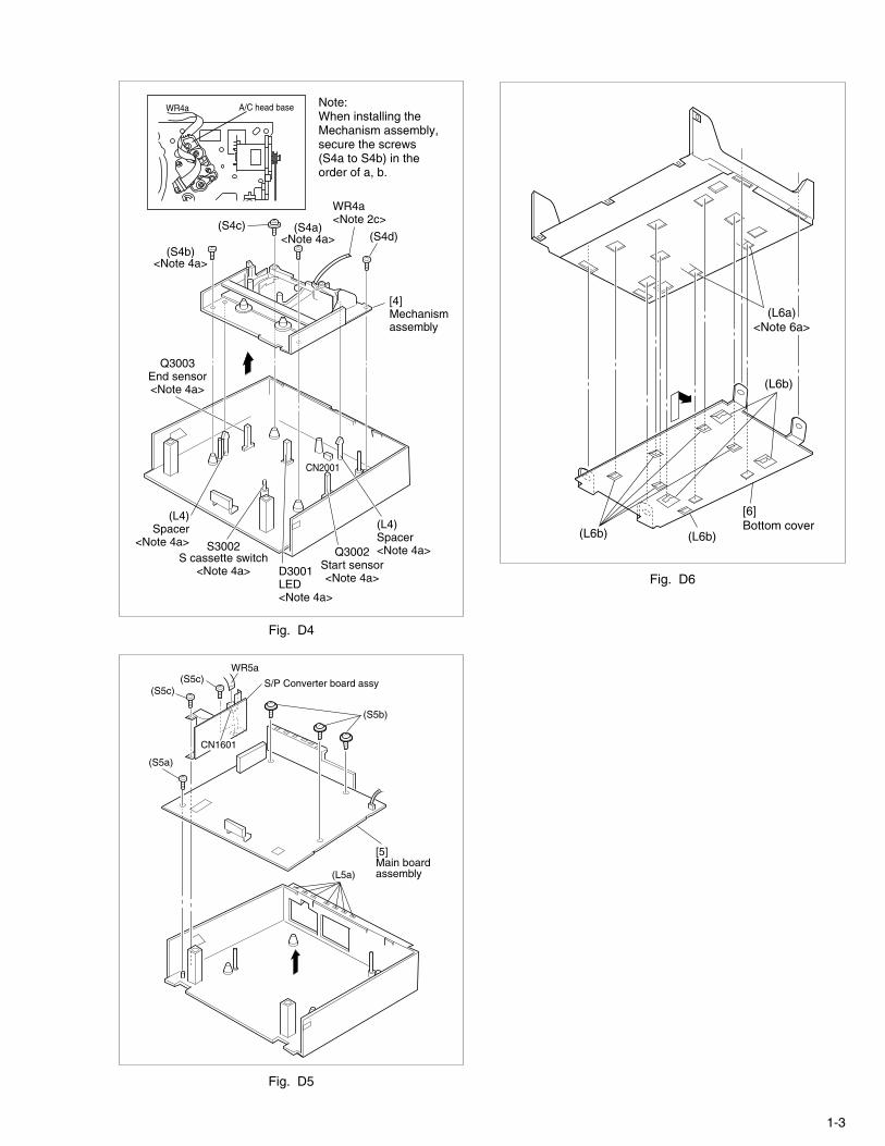
[1] Top cover, D1 4(S1a), (S1b)Bracket 2(S1c)
[2] Front panel assembly D2 CN7001(WR2a), <Note 2a>CN916(WR2b), <Note 2b>4(L2a), 3(L2b) <Note 2c>
ADV. Jog board assembly 2(S2a)S Jack board assembly 2(S2b)
[3] Drum assembly D3 CON1(WR3a), <Note 2c>CN1(WR3b),(S3a), (S3b), (S3c)
(Inertia plate) 4(L3a)(Roller arm assy) (P3), (L3b)
[4] Mechanism assembly D4 CN2001(WR4a), <Note 2c>(S4a),(S4b), <Note 4a>(S4c), (S4d), 2(L4)
[5] S/P Converter board D5 CN601(WR5a), <Note 2c>assembly 2(S5c)Main board assembly (S5a),3(S5b),7(L5a)
[6] Bottom cover D6 2(L6a), 9(L6b) <Note 6a>
SECTION 1DISASSEMBLY
1.3 Disassembly/assembly method1.1 Disassembly flow chart
This flowchart lists the disassembling steps for the cabinetparts and P.C. boards in order to gain access to item(s) tobe serviced. When reassembling, perform the step(s) in re-verse order. Bend, route and dress the flat cables as theywere originally laid.
1.2 How to read the disassembly and assembly
Note:• The bracketed ( ) WR of the connector symbol are as-
signed nos. in priority order and do not correspond tothose on the spare parts list.
(5) Adjustment information for installation
Top cover, Bracket
Front panel assembly,ADV. Jog board assembly,
S Jack board assembly
Drum assembly
Mechanism assembly
S/P Converter board assembly,Main board assembly
Bottom cover
[1]
[2]
[3]
[4]
[5]
[6]
Step/Loc No. Part Name
Fig.No. Point Note
- - - - - - - - - - - - - - - - -
(1) (2) (3) (4) (5)
Step/Loc No. Part Name
Fig.No. Point Note
[1] Top cover, D1 4(S1a),(S1b),3(L1a), <Note 1a>2(SD1a),(P1a),(W1a),CN1(WR1a),
Bracket 2(S1c)
<Example>
(1) Order of steps in ProcedureWhen reassembling, perform the step(s) in the reverse order.These numbers are also used as the identification (location) No.of parts Figures.
(2) Part name to be removed or installed.(3) Fig. No. showing procedure or part location.(4) Identification of part to be removed, unhooked, unlocked,
released, unplugged, unclamped or unsoldered.P= Spring, W= Washer, S= Screw, L= Locking tab, SD= Solder,CN**(WR**)= Remove the wire (WR**) from the connector(CN**).
<Note 2a>• When reattaching the Front panel assembly, make sure that
the door opener “a” of the Cassette holder assembly is low-ered in position prior to the reinstallation.
<Note 2b>• When reattaching the Front panel assembly, pay careful at-
tention to the switch lever not to make it touch the switchknob “b” of the Main board assembly from the side.
<Note 2c>• Be careful not to damage the connector and wire etc. during
connection and disconnection.When connecting the wire to the connector, be careful withthe wire direction.
<Note 4a>• When it is required to remove the screws (S4a to S4b) re-
taining the Mechanism assembly, please refer to the “Pro-cedures for Lowering the Cassette holder assembly”(Seeon page 1-2).
• When reattaching the Mechanism assembly to the Mainboard assembly, take care not to damage the sensors andswitch on the Main board assembly.
• When removing the Mechanism assembly only, unhook thetwo spacers connecting it with the Main board assemblywith pliers from the back side of the Main board assemblyfirst, and then remove the Mechanism assembly.
• The wire (WR4a) has excess length that may be loose, as itis quite long. After inserting the wire and connectors, theloose portion of the wire should be taken up and accommo-dated between the A/C head base and the main deck.
<Note 6a>When removing the bottom cover, push down the two tabs(L6a) to slide the bottom cover.
- - - - - - - - - - - - - - - - -

1-2
(L2a)
(L2b)
WR2a<Note 2c>
(L2a)
CN7001
CN916
[2] Front panel assembly
a <Note 2a>
b <Note 2b>WR2b<Note 2c>
CN7108
(S2b)
S Jackboard assembly
WR2b<Note 2c>
Front panelback side
(S2a) ADV. Jog board assembly
WR2a<Note 2c>
Front panelback side
CN7003
Fig. D1 Fig. D3
Fig. D2
Fig. 1
Fig. 2
Fig. 3
(A)(B)
Procedures for Lowering the Cassette holder assemblyAs the mechanism of this unit is integrated with the Housingassembly, the holder must be lowered and the two screws un-screwed when removing the Mechanism assembly.
(S1a)
(S1a)
(S1a)
(S1c)
(S1c)
Bracket
[1] Top cover
[1]
(S1b)
Procedures for Lowering the Cassette holder assembly
(S3b)
[3]Drum assembly
CN1
CON1
WR3a<Note 2c>(L3a)
(L3b)
(P3)
Roller armassy
Inertia plate
(L3c)
WR3b<Note 2c>
Cleaner assy
Not used
Not used
(S3a) (S3c)
Drum shield
(S3d)
Note: When installing the Drum assembly, secure the screws(S3a to S3c) in the order of a, b, c.
Turn the loading motor pulley in the direction as indicated byFig.2. As both (A) and (B) levers are lodged twice, push thelevers in the direction as indicated by Fig.3 to release them.When pushing the levers, do it in the order of (A), (B), (B),(A). When the holder has been lowered, turn the pulley untilthe cassette holder is securely in place without allowing anyup/down movement.
1-3
[4]Mechanismassembly
Q3003End sensor<Note 4a>
Q3002Start sensor<Note 4a>
(S4b)<Note 4a>
(S4a)<Note 4a>
(S4c)(S4d)
D3001LED<Note 4a>
(L4)Spacer
<Note 4a>
CN2001
A/C head baseWR4a Note: When installing the Mechanism assembly, secure the screws (S4a to S4b) in the order of a, b.
(L4)Spacer<Note 4a>
WR4a<Note 2c>
S3002S cassette switch
<Note 4a>
Fig. D4
Fig. D6
Fig. D5
[5]Main board assembly(L5a)
(S5a)
(S5c)(S5c)
WR5a
(S5b)
S/P Converter board assy
CN1601
(L6b)
[6]Bottom cover
(L6b)
(L6b)
(L6a)<Note 6a>

1-4
1.4 Service position
This unit has been designed so that the Mechanism andMain board assemblies can be removed together from thechassis assembly. Before diagnosing or servicing the cir-cuit boards, take out the major parts from the chassis as-sembly.
1.4.1 How to set the “Service position”
(1) Refer to the disassembly procedure and perform the dis-assembly of the major parts before removing the Drumassembly.
(2) Lower the cassette holder to prepare for the removal ofthe Mechanism assembly screws. (Refer to the “Proce-dures for lowering the Cassette holder assembly” of 1.3Disassembly/assembly method.)
(3) Remove the combined Mechanism and Main board as-semblies.
(4) Connect the wires and connectors of the major parts thathave been removed in step (1). (Refer to Fig.1-4-1a.)
(5) Place the combined Mechanism and Main board assem-blies upside down.
(6) Insert the power cord plug into the power outlet and thenproceed with the diagnostics and servicing of the boardassembly.
Notes:• Before inserting the power cord plug into the power
outlet, make sure that none of the electrical parts areable to short-circuit between the workbench and theboard assembly.
• For the disassembly procedure of the major parts anddetails of the precautions to be taken, see “1.3 Disas-sembly/assembly method”.
• If there are wire connections from the Main board andMechanism assemblies to the other major parts, besure to remove them ( including wires connected to themajor parts ) first before performing step (2).
• When carrying out diagnosis and repair of the Main boardassembly in the “Service position”, be sure to groundboth the Main board and Mechanism assemblies. If theyare improperly grounded, there may be noise on the play-back picture or FDP counter display may move evenwhen the mechanism is kept in an inoperative status.
• In order to diagnose the playback or recording of the cas-sette tape, set the Mechanism assembly to the requiredmode before placing it upside down. If the mechanismmode is changed (including ejection) while it is in an up-side down position the tape inside may be damaged.
1.5 Mechanism service mode
This model has a unique function to enter the mechanisminto every operation mode without loading of any cassettetape. This function is called the “Mechanism service mode”.
1.5.1 How to set the “Mechanism service mode”(1) Unplug the power cord plug from the power outlet.(2) Connect TPGND and TP7001(TEST) on the Main board
assembly with a jump wire.(3) Insert the power cord plug into the power outlet.(4) With lock levers (A) (B) on the left and right of the Cas-
sette holder assembly pulled toward the front, slide theholder in the same direction as the cassette insertion di-rection. (For the positions of lock levers (A) (B), refer tothe “Procedures for lowering the Cassette holder assem-bly” of 1.3 Disassembly/assembly method.)
(5) The cassette holder lowers and, when the loading hascompleted, the mechanism enters the desired mode.
1.6 Jig RCU mode
This unit uses the following two modes for receiving remotecontrol codes.1) User RCU mode : Ordinary mode for use by the user.2) Jig RCU mode : Mode for use in production and serv-
icing.
When using the Jig RCU, it is required to set the VCR tothe Jig RCU mode (the mode in which codes from the JigRCU can be received). As both of the above two modesare stored in the EEPROM, it is required to set the VCRback to the User RCU mode each time that an adjustmentis made or to check that the necessary operations havebeen completed. These modes can be set by the opera-tions described below.
1.6.1 Setting the Jig RCU mode(1) Unplug the power cord plug from the power outlet.(2) Press and hold the “REC” and “PAUSE” buttons on the
VCR simultaneously, while plugging the power cord pluginto the power outlet.When the VCR is set to the Jig RCU mode, the symbols( “ : ” ) in the time display of the FDP are turned off.
1.6.2 Setting the User RCU mode(1) Turn off the power.(2) Press the “REC” and “PAUSE” buttons of the VCR si-
multaneously. Alternatively, transmit the code “80” fromthe Jig RCU.
1.7 Servicing items related to video navigation
The video navigation function built into this unit works bystoring the video navigation data in the internal EEPROMand writing data in the cassette tape simultaneously.The video navigation data stored in the EEPROM cannot becopied to another EEPROM. Therefore, when the circuit boardmounting the EEPROM is replaced, the original EEPROMshould be mounted on the new board. This will make the us-er’s video navigation data usable with the new circuit boardafter replacement. However, the user’s data cannot be restoredif the EEPROM on the original circuit board is damaged.
Note:• If the circuit board mounting the EEPROM or the
EEPROM alone has been replaced, it is required to per-form confirmation/re-adjustment on all of the adjust-ment items using the EVR as well as those which areadjusted by transmitting adjustment codes from the JigRCU.Fig. 1-4-1a
CP3002
TP7001TEST
CN7001
CN7002
CN7005
CN7003
CN916
TPGND
TP2253A.PB.FM
TP4001CTL. P
CN511
CN1601
TP106PB. FM
TP111D.FF Main
boardassembly
VR1201D/A LEVEL ADJ
VR1401D/A LEVEL ADJ
C3025Timer Clock
ADV. Jog board assembly
Mini front board assembly2D Digital boardassembly3D Digital/2M boardassembly
Demodulator boardassembly
S Jack boardassembly
Terminal board assembly
S/P Converterboard assembly
ONLY USED FOR HR-S8850MS
ONLY USED FORHR-S7850MS/S7851MS/S8850MS
1-5
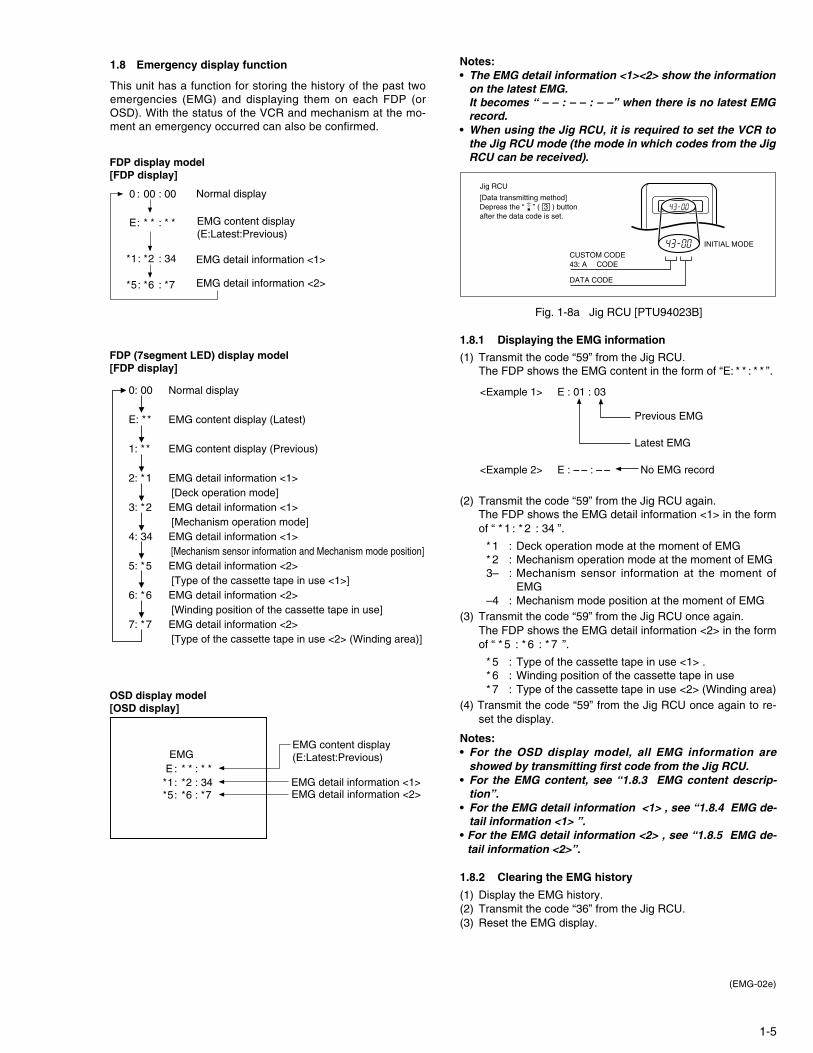
1.8 Emergency display function
This unit has a function for storing the history of the past twoemergencies (EMG) and displaying them on each FDP (orOSD). With the status of the VCR and mechanism at the mo-ment an emergency occurred can also be confirmed.
Fig. 1-8a Jig RCU [PTU94023B]
(2) Transmit the code “59” from the Jig RCU again.The FDP shows the EMG detail information <1> in the formof “ * 1 : * 2 : 34 ”.
* 1 : Deck operation mode at the moment of EMG* 2 : Mechanism operation mode at the moment of EMG3– : Mechanism sensor information at the moment of
EMG–4 : Mechanism mode position at the moment of EMG
(3) Transmit the code “59” from the Jig RCU once again.The FDP shows the EMG detail information <2> in the formof “ * 5 : * 6 : * 7 ”.
* 5 : Type of the cassette tape in use <1> .* 6 : Winding position of the cassette tape in use* 7 : Type of the cassette tape in use <2> (Winding area)
(4) Transmit the code “59” from the Jig RCU once again to re-set the display.
Notes:• For the OSD display model, all EMG information are
showed by transmitting first code from the Jig RCU.• For the EMG content, see “1.8.3 EMG content descrip-
tion”.• For the EMG detail information <1> , see “1.8.4 EMG de-
tail information <1> ”.• For the EMG detail information <2> , see “1.8.5 EMG de-
tail information <2>”.
1.8.2 Clearing the EMG history
(1) Display the EMG history.(2) Transmit the code “36” from the Jig RCU.(3) Reset the EMG display.
<Example 1> E : 01 : 03
Previous EMG
Latest EMG
No EMG record<Example 2> E : – – : – –
1.8.1 Displaying the EMG information
(1) Transmit the code “59” from the Jig RCU.The FDP shows the EMG content in the form of “E: * * : * * ”.
INITIAL MODE
DATA CODE
CUSTOM CODE43: A CODE
[Data transmitting method]Depress the “ ” ( 3 ) button after the data code is set.
Jig RCU
Notes:• The EMG detail information <1><2> show the information
on the latest EMG.It becomes “ – – : – – : – –” when there is no latest EMGrecord.
• When using the Jig RCU, it is required to set the VCR tothe Jig RCU mode (the mode in which codes from the JigRCU can be received).FDP display model
[FDP display]
0 : 00 : 00
E: * * : * *
*1: *2 : 34
*5: *6 : *7
E : * * : * * *1: *2 : 34 *5: *6 : *7
EMG detail information <2>
EMG detail information <2>EMG detail information <1>
EMG detail information <1>
EMG content display (E:Latest:Previous)
Normal display
OSD display model[OSD display]
EMGEMG content display (E:Latest:Previous)
FDP (7segment LED) display model [FDP display]
0: 00
E: **
1: **
2: *1
3: *2
4: 34
5: *5
6: *6
7: *7
Normal display EMG content display (Latest) EMG content display (Previous) EMG detail information <1> [Deck operation mode] EMG detail information <1> [Mechanism operation mode] EMG detail information <1> [Mechanism sensor information and Mechanism mode position] EMG detail information <2> [Type of the cassette tape in use <1>] EMG detail information <2> [Winding position of the cassette tape in use] EMG detail information <2> [Type of the cassette tape in use <2> (Winding area)]
(EMG-02e)

1-6
1.8.3 EMG content description
Note: EMG contents “E08/E09” are for the model with Dynamic Drum (DD).
Table 1-8-3a
When the mechanism mode cannot be changed to an-other mode even when the loading motor has rotatedfor more than 4 seconds in the loading direction, [E:01]is identified and the power is turned off.
When the mechanism mode cannot be changed to an-other mode even when the loading motor has rotatedfor more than 4 seconds in the unloading direction, [E:02]is identified and the power is turned off.
When the take-up reel pulse has not been generated formore than 4 seconds in the capstan rotating mode, [E:03]is identified, the pinch rollers are turned off and stopped,and the power is turned off. However, the reel EMG isnot detected in STILL/SLOW modes.
When the drum FG pulse has not been input for morethan 3 seconds in the drum rotating mode, [E:04] is iden-tified, the pinch rollers are turned off and stopped, andthe power is turned off.
When the eject operation does not complete in 3 sec-onds after the start, [E:05] is identified, the pinch rollersare turned off and stopped, and the power is turned off.When the cassette insertion operation does not completein 3 seconds after the start, the cassette is ejected. Inaddition, when the operation does not complete within3 seconds after the start, [E:05] is also identified and thepower is turned off immediately.
When the capstan FG pulse has not been generated formore than 1 second in the capstan rotating mode, [E:06]is identified, the pinch rollers are turned off and stopped,and the power is turned off.However, the capstan EMGis not detected in STILL/SLOW/FF/REW modes.
When short-circuiting of the SW power supply with GNDhas lasted for 0.5 second or more, [E:07] is identified,all the motors are stopped and the power is turned off.
When DD tilting does not complete in 4 seconds, [E:08]is identified, the tilt motor is stopped and the power isturned off.
When the DD FG pulse is not generated within 2.5 sec-onds, [E:09] is identified, the tilt motor is stopped andthe power is turned off.
When the supply reel pulse has not been generated formore than 10 seconds in the capstan rotating mode,[E:0A] is identified and the cassette is ejected (but thepower is not turned off). However, note that the reel EMGis not detected in the SLOW/STILL mode.
1. The mechanism is locked in the middle of mode transition.2. The mechanism is locked at the loading end due to the encoder position
reading error during mode transition.3. Power is not supplied to the loading MDA.
1. The mechanism is locked in the middle of mode transition.2. The mechanism is locked at the unloading end due to the encoder posi-
tion reading error during mode transition.3. Power is not supplied to the loading MDA.
1. The take-up reel pulse is not generated in the FWD transport modes (PLAY/FWD SEARCH/FF, etc.) because;1) The idler gear is not meshed with the take-up reel gear;2) The idler gear is meshed with the take-up reel gear, but incapable of wind-
ing due to too large mechanical load (abnormal tension);3) The take-up reel sensor does not output the FG pulse.
2. The supply reel pulse is not generated in the REV transport modes (REVSEARCH/REW, etc.) because;1) The idler gear is not meshed with the supply reel gear.2) The idler gear is meshed with the supply reel gear, but incapable of wind-
ing due to too large a mechanical load (abnormal tension);3) The supply reel sensor does not output the FG pulse.
3. Power is not supplied to the reel sensors.
1. The drum could not start or the drum rotation has stopped due to too largea load on the tape, because;1) The tape tension is abnormally high;2) The tape is damaged or a foreign object (grease, etc.) adheres to the tape.
2. The drum FG pulse did not reach the System controller CPU because;1) The signal circuit is disconnected in the middle;2) The FG pulse generator (hall device) of the drum is faulty.
3. The drum control voltage (DRUM CTL V) is not supplied to the MDA.4. Power is not supplied to the drum MDA.
1. The cassette cannot be ejected due to a failure in the drive mechanism ofthe housing.
2. When the housing load increases during ejection, the loading motor isstopped because of lack of headroom in its drive torque.
Housing load increasing factors: Temperature environment (low tempera-ture, etc.), mechanism wear or failure.
3. The sensor/switch for detecting the end of ejection are not functioning normally.4. The loading motor drive voltage is lower than specified or power is not sup-
plied to the motor (MDA).5. When the user attempted to eject a cassette, a foreign object (or perhaps
the user's hand) was caught in the opening of the housing.
1. The capstan could not start or the capstan rotation has stopped due to toolarge a load on the tape, because;1) The tape tension is abnormally high (mechanical lock);2) The tape is damaged or a foreign object (grease, etc.) is adhered to the
tape (occurrence of tape entangling, etc.).2. The capstan FG pulse did not reach the System controller CPU because;
1) The signal circuit is disconnected in the middle;2) The FG pulse generator (MR device) of the capstans is faulty.
3. The capstan control voltage (CAPSTAN CTL V) is not supplied to the MDA.4. Power is not supplied to the capstan MDA.
1. The SW 5 V power supply circuit is shorted with GND.2. The SW 12 V power supply circuit is shorted with GND.
1. The absolute value sensor is defective. (The soldered parts have separated.)2. The pull-up resistor at the absolute sensor output is defective. (The soldered parts
have separated.)3. Contact failure or soldering failure of the pins of the connector (board-to-board) to the
absolute value sensor.4. The absolute value sensor data is not sent to the System Controller CPU.
1. The FG sensor is defective. (The soldered parts have separated.)2. The pull-up resistor at the FG sensor output is defective. (The soldered parts have
separated.)3. Contact failure or soldering failure of the pins of the connector (board-to-board) to the FG sensor.4. The power to the sensor is not supplied. (Connection failure/soldering failure)5. The FG pulse is not sent to the System Controller CPU.6. The tilt motor is defective. (The soldered parts have separated.)7. The drive power to the tilt motor is not supplied. (Connection failure/soldering failure)8. The tilt motor drive MDA - IC is defective.9. Auto-recovery of the DD tilting cannot take place due to overrun.
1. The supply reel pulse is not generated in the FWD transport mode (PLAY/FWD SEARCH/FF, etc.) because;1) PLAY/FWD or SEARCH/FF is started while the tape in the inserted cas-
sette is cut in the middle;2) A mechanical factor caused tape slack inside and outside the supply
reel side of the cassette shell. In this case, the supply reel will not rotateuntil the tape slack is removed by the FWD transport, so the pulse is notgenerated until then;
3) The FG pulse output from the supply reel sensor is absent.2. The take-up reel pulse is not generated in the REV transport mode (REV
SEARCH/REW, etc.).1) REV SEARCH/REW is started when the tape in the inserted cassette
has been cut in the middle;2) A mechanical factor caused tape slack inside and outside the take-up
reel side of the cassette shell. In this case, the supply reel will not rotateuntil the tape slack is removed by the REV transport, so the pulse willnot be generated until that time;
3) The FG pulse output from the take-up reel sensor is absent.3. The power to a reel sensor is not supplied.
FDP CONTENT CAUSE
Presupposing the presence of the control pulse output in the PLAY mode, when the value obtained by mixing the two V.FM outputchannels (without regard to the A.FM output) has remained below a certain threshold level for more than 10 seconds, [E:C1] or [E:U1]is identified and recorded in the emergency history. During the period in which a head clog is detected, the FDP and OSD repeat the“3-second warning display” and “7-second noise picture display” alternately.
EMG code : “E:C1” or “E:U1” / FDP : “U:01” / OSD : “Try cleaning tape.” or “Use cleaning cassette.”The head clog warning is reset when the above-mentioned threshold has been exceeded for more than 2 seconds or the mode ischanged to another mode than PLAY.
EC1 or EU1:Head clog warning
E0A:Supply ReelPulse EMG
E07: SW PowerShort-CircuitEMG
E06: Capstan FGEMG
E05: Cassette EjectEMG
E04: Drum FGEMG
E03: Take Up ReelPulse EMG
E02: Unloading EMG
E01: Loading EMG
E08: DD Initialized(AbsolutePositionSensor)EMG
E09: DD FG EMG

1-7
1.8.4 EMG detail information <1>
The status (electrical operation mode) of the VCR and the sta-tus (mechanism operation mode/sensor information) of themechanism in the latest EMG can be confirmed based on thefigure in EMG detail information <1> .
[FDP/OSD display]
* 1 : * 2 : 34
* 1 : Deck operation mode at the moment of EMG * 2 : Mechanism operation mode at the moment of EMG 3– : Mechanism sensor information at the moment of EMG –4 : Mechanism mode position at the moment of EMG
Note:• For EMG detailed information <1>, the content of the code
that is shown on the FDP (or OSD) differs depending onthe parts number of the system control microprocessor(IC3001) of the VCR. The system control microprocessorparts number starts with two letters, refer these to the cor-responding table.
* 1 : Deck operation mode[Common table of MN*, HD* and M3*]
00 - Mechanism being initialized01 00 STOP with pinch roller pressure off (or tape present with P.OFF)02 01 STOP with pinch roller pressure on03 - POWER OFF as a result of EMG04 04 PLAY0C 0E REC10 11 Cassette ejected20 22 FF21 - Tape fully loaded, START sensor ON, short FF22 - Cassette identification FWD SEARCH before transition to FF (SP
x7-speed)24 26 FWD SEARCH (variable speed) including x2-speed2C 2E INSERT REC40 43 REW42 - Cassette identification REV SEARCH before transition to REW (SP
x7-speed)44 47 REV SEARCH (variable speed)4C 4C AUDIO DUB6C 6E INSERT REC (VIDEO + AUDIO)84 84 FWD STILL / SLOW85 85 REV STILL / SLOW8C 8F REC PAUSE8D - Back spacing8E - Forward spacing (FWD transport mode with BEST function)AC AF INSERT REC PAUSEAD - INSERT REC back spacingCC CD AUDIO DUB PAUSECD - AUDIO DUB back spacingEC EF INSERT REC (VIDEO + AUDIO) PAUSEED - INSERT REC (VIDEO + AUDIO) back spacing
* 2 : Mechanism operation mode[Common table of MN* and M3*]
[Table of HD*]Display Mechanism operation mode
00 STOP with pinch roller pressure off01 STOP with pinch roller pressure on02 U/L STOP (or tape being loaded)04 PLAY05 PLAY (x1-speed playback using JOG)0E REC11 Cassette ejected22 FF26 FWD SEARCH (variable speed) including x2-speed2E INSERT REC43 REW47 REV SEARCH4C AUDIO DUB6E INSERT REC (VIDEO + AUDIO)84 FWD STILL/SLOW85 REV STILL/SLOW8F REC PAUSEAF INSERT REC PAUSEC7 REV SEARCH (x1-speed reverse playback using JOG)CD AUDIO DUB PAUSEEF INSERT REC (VIDEO + AUDIO) PAUSEF0 Mechanism being initializedF1 POWER OFF as a result of EMGF2 Cassette being insertedF3 Cassette being ejectedF4 Transition from STOP with pinch roller pressure on to STOP with pinch
roller pressure offF5 Transition from STOP with pinch roller pressure on to PLAYF6 Transition from STOP with pinch roller pressure on to RECF7 Cassette type detection SEARCH before FF/REW is being executedF8 Tape being unloadedF9 Transition from STOP with pinch roller pressure off to STOP with pinch
roller pressure onFA Transition from STOP with pinch roller pressure off to FF/REWFB Transition from STOP with pinch roller pressure off to REC.P (T.REC,etc.)FC Transition from STOP with pinch roller pressure off to cassette type de-
tection SEARCHFD Short REV being executed after END sensor on during unloadingFE Tension loosening being executed after tape loading (STOP with pinch
roller pressure on)
DisplayDeck operation mode
MN*/M3* HD*
00 00 Command standby (Status without executing command)02 02 POWER OFF by EMG occurrence04 04 Moving to the adjacent position in the LOAD direction06 06 Moving to the adjacent position in the UNLOAD direction08 08 Cassette ejection being executed / Cassette housing ejection being
executed- 0A Mode transition to STOP with cassette ejection end
0A 0C Cassette insertion being executed0C 0E Tape being loaded0E 10 Tape being unloaded10 12 Mode transition to STOP with pinch roller compression ON12 14 Mode transition to STOP with pinch roller compression OFF14 16 Mode transition to STOP with pinch roller compression OFF as a result
of POWER OFF16 18 Mode transition to STOP with pinch roller compression ON as a result
of POWER ON18 1A Mode transition to PLAY1A 1C Mode transition to FWD SEARCH1C 1E Mode transition to REC1E 20 Mode transition to FWD STILL / SLOW20 22 Mode transition to REV STILL / SLOW22 24 Mode transition to REV SEARCH24 26 Mode transition from FF / REW to STOP26 28 Mode transition to FF28 2A Mode transition to REW2A 2C 4 sec. of REV as a result of END sensor going ON during loading2C 2E Short FF / REV as a result of END sensor going ON during unloading2E 30 Mechanism position being corrected due to overrun80 80 Mechanism in initial position (Dummy command)
DisplayMechanism operation mode
MN* M3*

1-8
-0 -7 - Initial value-1 -0 - EJECT position- - -0 EJECT position (Cassette housing drive mode)-2 -7 - Housing operating- - -1 Between EJECT and U / L STOP-3 -1 -2 U / L STOP position- - -3 Guide arm drive position
-4 -7 -4 Tape being loaded / unloaded (When the pole base islocated on the front side of the position just beside thedrum)
-5 -2 -5 Tape being loaded / unloaded (When the pole base islocated on the rear side of the position just beside thedrum)
-6 -7 -6 Pole base compressed position-7 -3 -F FF / REW position-8 -7 -F Between FF / REW and STOP with pinch roller compres-
sion ON-9 -4 -F STOP with pinch roller compression OFF-A -7 -E Between STOP with pinch roller compression OFF and
REV-B -5 - REV (REV STILL / SLOW) position- - -D REV position- - -C Between REV and REV STILL / SLOW- - -B REV STILL / SLOW position
-C -7 - Between REV and FWD- - -A Between REV STILL / SLOW and FWD STILL / SLOW
-D -6 - FWD (FWD STILL / SLOW) position- - -9 FWD STILL / SLOW position
-E -7 - Between FWD and PLAY- - -8 Between FWD STILL / SLOW and PLAY
-F -6 -7 PLAY position
0- VHS Cassette insertion Tab broken ON ON1- VHS Cassette insertion Tab broken ON OFF2- VHS Cassette insertion Tab broken OFF ON3- VHS Cassette insertion Tab broken OFF OFF4- VHS Cassette insertion Tab present ON ON5- VHS Cassette insertion Tab present ON OFF6- VHS Cassette insertion Tab present OFF ON7- VHS Cassette insertion Tab present OFF OFF8- S-VHS Cassette ejection Tab broken ON ON9- S-VHS Cassette ejection Tab broken ON OFFA- S-VHS Cassette ejection Tab broken OFF ONB- S-VHS Cassette ejection Tab broken OFF OFFC- S-VHS Cassette ejection Tab present ON OND- S-VHS Cassette ejection Tab present ON OFFE- S-VHS Cassette ejection Tab present OFF ONF- S-VHS Cassette ejection Tab present OFF OFF
3– : Mechanism sensor information[Common table of MN*, HD* and M3*]
Mechanism sensor information Display MN* / HD* M3* REC safety Start End
S-VHS SW CASS SW SW sensor sensor
* 6 : Cassette tape winding position
The cassette tape winding position at the moment of EMG isdisplayed by dividing the entire tape (from the beginning to theend) in 22 sections using a hex number from “00” to “15”.
“00” : End of winding“15” : Beginning of winding“FF or – – ” : Tape position not identified
–4 : Mechanism mode position[Common table of MN*, HD* and M3*]
Display Mechanism mode position
MN* HD* M3*
Note:• The values of cassette tape type <2> in the above table
are typical values with representative cassette tapes.
* 7 : Cassette tape type <2> (Winding area)
Display Cassette tape type <2>
00 Cassette type not identified07 Small reel, thick tape T-5
08 - 0E C cassette, thick tape TC-1009 - 15 C cassette, thick tape TC-20P0A - 0B Small reel, thick tape T-200A - 16 C cassette, thin tape TC-300A - 16 C cassette, thin tape TC-400D - 0F Small reel, thick tape T-4011 - 14 Small reel, thick tape T-6015 - 18 Small reel, thick tape T-80 / DF-16017 - 1A Small reel, thick tape T-90 / DF-18019 - 1D Small reel, thick tape T-1001D - 21 Small reel, thick tape T-120 / DF-2401E - 1F Small reel, thin tape T-1401F - 23 Small reel, thick tape T-13021 - 23 Small reel, thin tape T-16021 - 23 Small reel, thin tape T-16822 - 24 Small reel, thick tape DF-30022 - 24 Small reel, thin tape T-180 / DF-36022 - 24 Small reel, thin tape T-210 / DF-42022 - 23 Large reel T-523 - 24 Large reel T-1025 - 26 Large reel T-2027 - 29 Large reel T-3029 - 2B Large reel T-402D - 2F Large reel T-60
Notes:• Cassette tape type <1> is identified a few times during mode
transition and the identification count is variable depending onthe cassette tape type. If an EMG occurs in the middle of identi-fication, the cassette tape type may not be able to be identified.
• If other value than those listed in the above table is displayed,the cassette tape type is not identified.
Display Cassette tape type <1>
00 Cassette type not identified16 Large reel/small reel (T-0 to T-15/T-130 to T-210) not classified82 Small reel, thick tape (T-120) identified/thin tape (T-140) identified84 Large reel (T-0 to T-60) identified92 Small reel, thick tape (T-130) identified/thin tape (T-160 to T-210) identified93 Small reel, thick tape/C cassette (T-0 to T-100/C cassette) not classifiedC3 Small reel, thick tape/C cassette (T-0 to T-100/C cassette) being classifiedD3 Small reel, thick tape/C cassette (T-0 to T-100/C cassette) being classifiedE1 C cassette, thick tape (TC-10 to TC-20) identifiedE2 Small reel, thick tape (T-0 to T-100) identifiedE9 C cassette, thin tape (TC-30 to TC-40) identifiedF1 C cassette, thick tape/thin tape (TC-10 to TC-40) not classified
* 5 : Cassette tape type <1>
Note:• EMG detail information <2> is the reference information
stored using the remaining tape detection function of thecassette tape. As a result, it may not identify cassette cor-rectly when a special cassette tape is used or when thetape has variable thickness.
1.8.5 EMG detail information <2>
The type of the cassette tape and the cassette tape winding po-sition can be confirmed based on the figure in EMG detail infor-mation <2> .
[FDP/OSD display]
* 5 : * 6 : * 7* 5 : Type of the cassette tape in use <1>* 6 : Winding position of the cassette tape in use* 7 : Type of the cassette tape in use <2> (Winding area)
Note:• In the case of the "HD*” microprocessor, as the display is
always "-7” at any intermediate position between modes,the position of transitory EMG may sometimes not be lo-cated.
2-1
SECTION 2MECHANISM ADJUSTMENT
2.1 Before starting repair and adjustment
2.1.1 Precautions
(1) Unplug the power cord plug of the VCR before using yoursoldering iron.
(2) Take care not to cause any damage to the conductorwires when plugging and unplugging the connectors.
(3) Do not randomly handle the parts without identifyingwhere the trouble is.
(4) Exercise enough care not to damage the lugs, etc. dur-ing the repair work.
(5) When reattaching the front panel assembly, make surethat the door opener of the cassette holder assembly islowered in position prior to the reinstallation. (See SEC-TION 1 DISASSEMBLY.)
(6) When using the Jig RCU, it is required to set the VCR tothe Jig RCU mode (the mode in which codes from theJig RCU can be received). (See SECTION 1 DISASSEM-BLY.)
2.1.2 Checking for proper mechanical operations
Enter the mechanism service mode when you want to oper-ate the mechanism when no cassette is loaded. (See SEC-TION 1 DISASSEMBLY.)
2.1.3 Manually removing the cassette tape
1. In case of electrical failuresIf you cannot remove the cassette tape which is loaded be-cause of any electrical failure, manually remove it by takingthe following steps.
(1) Unplug the power cord plug from the power outlet.(2) Refer to the disassembly procedure and perform the dis-
assembly of the major parts before removing the drumassembly.
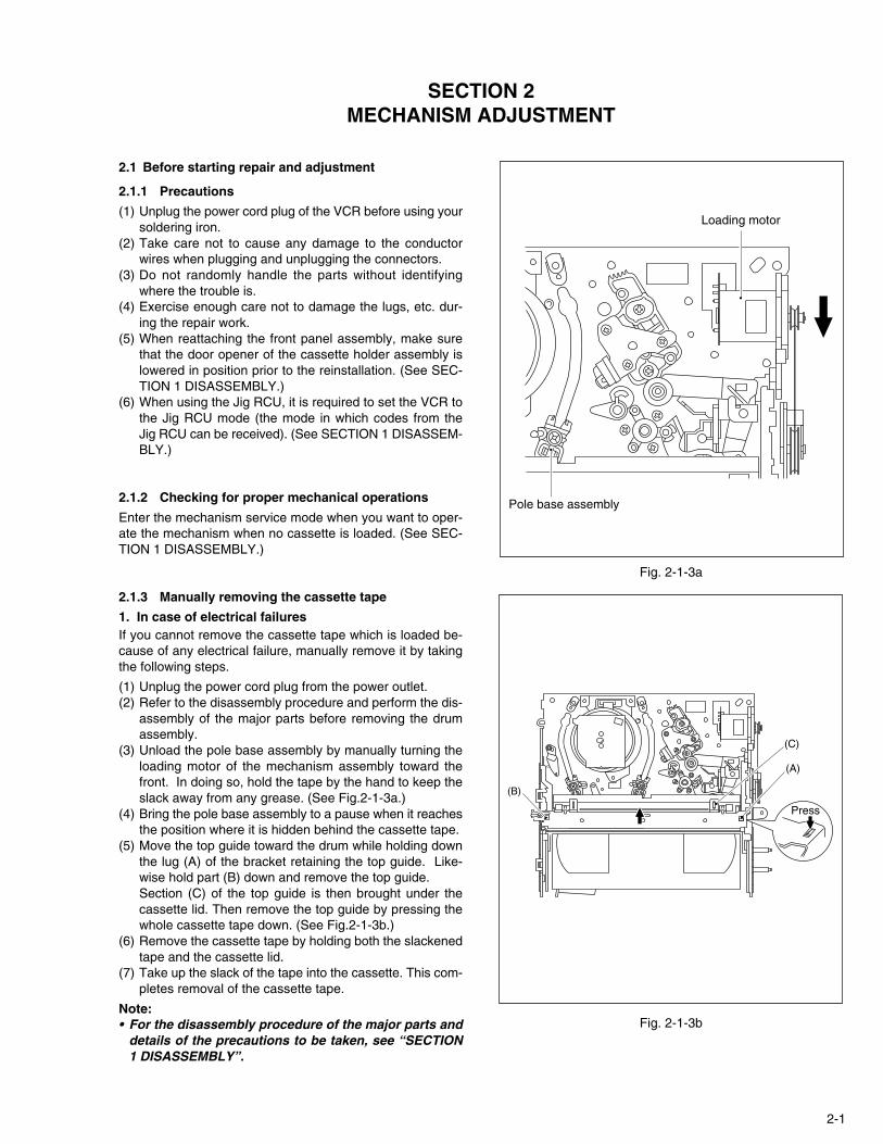
(3) Unload the pole base assembly by manually turning theloading motor of the mechanism assembly toward thefront. In doing so, hold the tape by the hand to keep theslack away from any grease. (See Fig.2-1-3a.)
(4) Bring the pole base assembly to a pause when it reachesthe position where it is hidden behind the cassette tape.
(5) Move the top guide toward the drum while holding downthe lug (A) of the bracket retaining the top guide. Like-wise hold part (B) down and remove the top guide.Section (C) of the top guide is then brought under thecassette lid. Then remove the top guide by pressing thewhole cassette tape down. (See Fig.2-1-3b.)
(6) Remove the cassette tape by holding both the slackenedtape and the cassette lid.
(7) Take up the slack of the tape into the cassette. This com-pletes removal of the cassette tape.
Note:• For the disassembly procedure of the major parts and
details of the precautions to be taken, see “SECTION1 DISASSEMBLY”.
Fig. 2-1-3b
Fig. 2-1-3a
Loading motor
Pole base assembly
Press
(C)
(A)
(B)

2-2
2. In case of mechanical failureIf you cannot remove the cassette tape which is loaded be-cause of any mechanical failure, manually remove it by tak-ing the following steps.(1) Unplug the power cable and remove the top cover, front
panel assembly and others so that the mechanism as-sembly is visible. (See SECTION 1 DASASSEMBLY.)
(2) While keeping the tension arm assembly of the mecha-nism assembly free from tension, pull the tape on the polebase assembly (supply or take-up side) out of the guideroller. (See Fig.2-1-3c.)
(3) Take the spring of the pinch roller arm assembly off thehook of the press lever assembly, and detach it from thetape. (See Fig.2-1-3d.)
(4) In the same way as in the electrical failure instructions in2.1.3-1(5), remove the top guide.
(5) Raise the cassette tape cover. By keeping it in that posi-tion, draw out the cassette tape case from the cassetteholder and take out the tape.
(6) By hanging the pinch roller arm assembly spring backon the hook, take up the slack of the tape into the cas-sette.
Fig. 2-1-3d
Fig. 2-1-3c
Pole base assembly (take-up side)
Pole base assembly (supply side)
Tension arm assembly
Guide pole guard
Pinch roller arm assembly
Press lever assembly
Take the spring off the hook, and detach it from the tape.
2.1.4 Jigs and tools required for adjustment
Roller driverPTU94002
A/C head positioning toolPTU94010
Back tension cassette gaugePUJ48076-2
Jig RCUPTU94023B
Torque gaugePUJ48075-2
Alignment tape(SP, stairstep, PAL)
MHPE
Alignment tape(LP, stairstep, PAL)
MHPE-L

2-3
2.1.5 Maintenance and inspection
1. Location of major mechanical partsIn this chapter, the two mechanism speeds are described by comparing the speeds of the standard type and the high-speedFF/REW type.It is possible to distinguish between these two types of mechanism by the diameters of their capstan pulleys.The capstan pulley diameter for the standard type is approx. 32 mm.The capstan pulley diameter for the high-speed FF/REW type is approx. 43 mm.For information on the different parts used in the two mechanism types, please refer to the “Replacement of major parts”.
Fig. 2-1-5a Mechanism assembly top side
Stator assembly
UV catcher2 (supply and take-up side)
Drum assemblyHead base
A/C head
Loading motor
Pinch roller arm assembly
Guide pole guard
Press lever assembly
Lid guide
Guide arm assembly
Reel disk (take-up side)
Sub brake assembly (take-up side)
Main brake assembly(take-up side)
Idler arm assemblyIdler lever
Main brake assembly(supply side)
Reel disk (supply side)
Rec safety lever
Tension brake assembly
Adjust pin
Tension arm assembly
Pole base assembly (supply side)
Full erase head
Pole base assembly (take-up side)
T1
T26
T25
T24
T23
T22
T2T3 T5 T7
T8
T9
T10
T11
T12
T13
T14
T15
T16T18T20
T17T19T21
T6
Fig. 2-1-5b Mechanism assembly bottom side
Belt (loading motor)
Capstan motor
Belt (capstan)
Capstan brake assembly
Loading arm gear (take-up side)
Loading arm gear (supply side)
Plate (supply side)
Control plate
Worm gear
Control cam
Cassette gear
Rotary encoder
Change lever assembly Clutch unit
Take-up leverTake-up head
Control bracket1
Tension arm bearing
B1
B22
B3 B5
B6
B7
B8
B9
B10
B12
B15
Rotary encoder guideB16
B17
B18
Brake leverB19
B20
B21
B14
B11
B4B2
Direct gearB13
Link lever

2-4
Guide rail Roller cam assemblyL2L1
Opener guide
Door opener
Drive gear
Cassette housing bracket
Limit gear
Worm gear
Belt (loading motor)
Loading motor
R2
R3 R5
R4
R1
Fig. 2-1-5c Mechanism assembly left side
Fig. 2-1-5d Mechanism assembly right side
5. Disassembling procedure tableThe following table indicates the order in which parts are re-moved for replacement. To replace parts, remove them inthe order of 1 to 18 as shown in the table. To install them,reverse the removal sequence.The symbols and numbers preceding the individual partnames represent the numbers in the “Location of major me-chanical parts” table. Also, the “T”, “B”, and “T/B” on the rightof each part name shows that the particular part is removedfrom the front, from the back, and from both sides of themechanism, respectively.
2. CleaningRegular cleaning of the transport system parts is desirablebut practically impossible. So make it a rule to carry out clean-ing of the tape transport system whenever the machine isserviced.When the video head, tape guide and/or brush get soiled,the playback picture may appear inferior or at worst disap-pear, resulting in possible tape damage.
(1) When cleaning the upper drum (especially the videohead), soak a piece of closely woven cloth or Kimu-wipewith alcohol and while holding the cloth onto the upperdrum by the fingers, turn the upper drumcounterclockwise.
Note:• Absolutely avoid sweeping the upper drum vertically
as this will cause damage to the video head.
(2) To clean the parts of the tape transport system other thanthe upper drum, use a piece of closely woven cloth or acotton swab soaked with alcohol.
(3) After cleaning, make sure that the cleaned parts are com-pletely dry before using the video tape.
3. LubricationWith no need for periodical lubrication, you have only to lu-bricate new parts after replacement. If any oil or grease oncontact parts is soiled, wipe it off and newly lubricate theparts.
Note:• See the “mechanism assembly” diagram of the parts
list for the lubricating or greasing spots, and for thetypes of oil or grease to be used.
~1000H ~2000H
Upper drum assembly ¤R R
A/C head ¤R ¤R
Lower drum assembly ¤ ¤R
Pinch roller arm assembly ¤ ¤
Full erase head ¤ ¤
Tension arm assembly ¤ ¤
Capstan motor (Shaft) ¤ ¤
Guide arm assembly ¤ ¤
Capstan motor R
Capstan brake assembly R
Main brake assembly R
Belt (Capstan) R R
Belt (Loading motor) R
Loading motor R
Clutch unit R
Worm gear R
Control plate R
Brush ¤R ¤R
Tension brake assembly R R
Rotary encoder R
4. Suggested servicing schedule for main componentsThe following table indicates the suggested period for suchservice measures as cleaning,lubrication and replacement.In practice, the indicated periods will vary widely accordingto environmental and usage conditions.However, the indi-cated components should be inspected when a set is broughtfor service and the maintenance work performed if neces-sary. Also note that rubber parts may deform in time,even ifthe set is not used.
Operation Hours System Parts Name
¤ : Cleaning
R : Inspection or replacement if necessary
Table 2-1-5a
Oth
erD
rive
Tap
e tr
ansp
ort

2-5
Symbols and numbers
Sym
bols
and
num
bers
Num
ber o
f rem
oval
ste
ps
Gui
de ra
il
Rol
ler c
am a
ssem
bly
Cas
sette
hou
sing
bra
cket
Ope
ner g
uide
Rel
ay g
ear
Cas
sette
hol
der a
ssem
bly
Driv
e ge
ar
Driv
e ar
m
Pin
ch ro
ller a
rm a
ssem
bly
Gui
de a
rm a
ssem
bly
Pre
ss le
ver a
ssem
bly
UV
cat
cher
2
Rot
ary
enco
der
Clu
tch
unit
Cha
nge
leve
r ass
embl
y
Dire
ct g
ear
Coup
ling
gear
Link
leve
r
Wor
m g
ear
Con
trol b
rack
et1
Con
trol p
late
Load
ing
arm
gea
r (su
pply
sid
e)
Load
ing
arm
gea
r (ta
ke-u
p si
de)
Take
-up
leve
r
Sub
brak
e as
sem
bly
(take
-up
side
)
Mai
n br
ake
asse
mbl
y (ta
ke-u
p si
de)
Ree
l dis
k (ta
ke-u
p si
de)
Tens
ion
brak
e as
sem
bly
Tens
ion
arm
ass
embl
y
Idle
r lev
er
Bra
ke le
ver (*1)
Fron
t (T)
/Bac
k (B
) of m
echa
nism
(Reference items) Replacement parts
Removal parts
L1
L1
L2
L2
R4
R1
R2
R5
R3
T9
T12
T11
T6
T7
B1
T1
T17
T10
T14
T15
T19
T13
T22
T20
T24
B9
T18
T16
B19
B16
B7
B8
B5
B4
B3
B11
B10
T25
B15
B12
B14
B13
B17
B18
B20
B21
R4 R1 R3 T9 T12 T11 B15 B12 B14 B13 B17 B21 B7 B8 B5 B4 B11 T14 T15 T13 T22 T24 T18 B19T1
2.2.3 Guide rail T 1
2.2.3 Roller cam assembly T 1
2.2.3 Cassette housing bracket T 1
2.2.3 Opener guide T 2
2.2.3 Door opener T 3
2.2.3 Relay gear T 3
2.2.3 Limit gear T 3
2.2.3 Cassette holder assembly T 6
2.2.3 Drive gear T 4
2.2.3 Drive arm T 8
2.2.4 Pinch roller arm assembly T 1
2.2.5 Guide arm assembly T 1
2.2.5 Press lever assembly T 3
2.2.6 A/C head T 1
2.2.7 Loading motor T 1
2.2.8 Capstan motor T/B 1
2.2.9 UV catcher2 T 1
2.2.9 Pole base assembly (take-up side) T/B 2
2.2.9 Pole base assembly (supply side) T/B 2
2.2.10 Rotary encoder B 1
2.2.11 Clutch unit B 1
2.2.12 Change lever assembly B 3
2.2.12 Direct gear B 4
2.2.12 Coupling gear B 5
2.2.12 Clutch gear B 6
2.2.13 Link lever B 1
2.2.14 Cassette gear B 2
2.2.14 Control cam B 2
2.2.14 Worm gear B 1
- Lid guide T/B 5
2.2.15Control bracket1 B 1
2.2.15Control plate B 6
2.2.16Loading arm gear (supply side) B 7
2.2.16Loading arm gear (take-up side) B 8
2.2.16Loading arm gear shaft B 9
2.2.17Take-up lever T/B 7
2.2.17Take-up head T/B 8
2.2.17Control plate guide T/B 8
2.2.18Capstan brake assembly T/B 7
2.2.19Sub brake assembly(take-up side) T/B 15
2.2.20Main brake assembly(take-up side) T/B 16
2.2.20Main brake assembly(supply side) T/B 9
2.2.20Reel disk (take-up side) T/B 16
2.2.21Tension brake assembly T/B 9
2.2.21Reel disk (supply side) T/B 10
2.2.21Tension arm assembly T/B 10
2.2.21Tension arm bearing T/B 10
2.2.22Idler lever T/B 17
2.2.22Idler arm assembly T/B 18
- Brake lever (*1) T/B 18
- Rotary encoder guide T/B 19 1 2 3 4 5 6 7 8 9 10 11 12 13 14 15 16 17 18
1 2 3 4 5 6 7 8 9 10 11 12 13 14 15 16 17
1 2 3 4 5 6 7 8 9 10 11 12 13 14 15 16 17
1 2 3 4 5 6 7 8 9 10 11 12 13 14 15 16
1 2 3 4 5 6 7 8 9
1 2 3 4 5 6 7 8 9
1 2 3 4 5 6 7 8 9
1 2 3 4 5 6 7 8 1 2 3 4 5 6 7 8 9 10 11 12 13 14 15
1 2 3 4 5 6 7 8
1 2 3 4 5 6 7 8 9 10 11 12 13 14 15
1 2 3 4
1 2
1 2
3
1 2 1
1
1
2 3
4 1 2 3 4 5
5 6
1 2 3 4 5 6
1 2 3 4 5 6
7
1 2
1 2
1 2
1
1
2
3
1 2 3
4 5
1 2 3 4 5
6 7
7
1 2 3 4 5 6
1 2 3 4 5 6
1 2 3 4 5 6 7
1 2 3 4 5 6
1 2 3 4 5
1 2 3 4
1
1
1
2
3 4
5
6
7
8
7
8 9 10 11 12 13 14
Table 2-1-5bNote:• The parts with marked ( * ) have different types of mecha-
nisms (standard type or high-speed FF/REW type).
* 1 : Uses the standard type mechanism only.
* 2 :Uses the high-speed FF/REW type mechanism only.
2-6
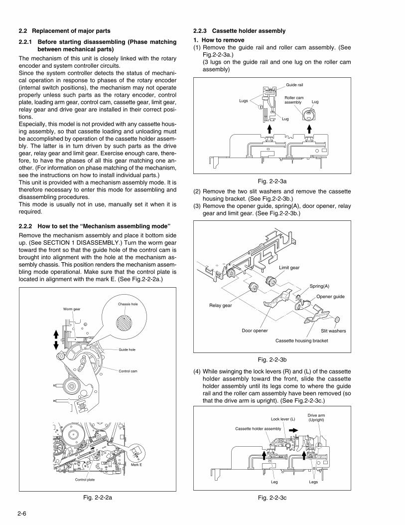
(4) While swinging the lock levers (R) and (L) of the cassetteholder assembly toward the front, slide the cassetteholder assembly until its legs come to where the guiderail and the roller cam assembly have been removed (sothat the drive arm is upright). (See Fig.2-2-3c.)
Fig. 2-2-3c
Cassette holder assembly
Lock lever (L)Drive arm(Upright)
Leg Legs
2.2.3 Cassette holder assembly
1. How to remove(1) Remove the guide rail and roller cam assembly. (See
Fig.2-2-3a.)(3 lugs on the guide rail and one lug on the roller camassembly)
Fig. 2-2-2a
Worm gear
Guide hole
Control cam
Chassis hole
Control plate
Mark E
Fig. 2-2-3b
(2) Remove the two slit washers and remove the cassettehousing bracket. (See Fig.2-2-3b.)
(3) Remove the opener guide, spring(A), door opener, relaygear and limit gear. (See Fig.2-2-3b.)
Fig. 2-2-3a
Lugs Lug
Lug
Guide rail
Roller cam assembly
Limit gear
Relay gear
Opener guide
Spring(A)
Cassette housing bracket
Slit washersDoor opener
2.2 Replacement of major parts
2.2.1 Before starting disassembling (Phase matchingbetween mechanical parts)
The mechanism of this unit is closely linked with the rotaryencoder and system controller circuits.Since the system controller detects the status of mechani-cal operation in response to phases of the rotary encoder(internal switch positions), the mechanism may not operateproperly unless such parts as the rotary encoder, controlplate, loading arm gear, control cam, cassette gear, limit gear,relay gear and drive gear are installed in their correct posi-tions.Especially, this model is not provided with any cassette hous-ing assembly, so that cassette loading and unloading mustbe accomplished by operation of the cassette holder assem-bly. The latter is in turn driven by such parts as the drivegear, relay gear and limit gear. Exercise enough care, there-fore, to have the phases of all this gear matching one an-other. (For information on phase matching of the mechanism,see the instructions on how to install individual parts.)This unit is provided with a mechanism assembly mode. It istherefore necessary to enter this mode for assembling anddisassembling procedures.This mode is usually not in use, manually set it when it isrequired.
2.2.2 How to set the “Mechanism assembling mode”
Remove the mechanism assembly and place it bottom sideup. (See SECTION 1 DISASSEMBLY.) Turn the worm geartoward the front so that the guide hole of the control cam isbrought into alignment with the hole at the mechanism as-sembly chassis. This position renders the mechanism assem-bling mode operational. Make sure that the control plate islocated in alignment with the mark E. (See Fig.2-2-2a.)

2-7
Fig. 2-2-3d
(5) While holding the left side of the cassette holder, lift thecassette holder assembly so that the three legs on theleft side are all released. Then pull the legs (A) and (B)on the right side out of the rail and also pull up the leg(C).(See Fig.2-2-3d and Fig.2-2-3e.)
(6) Draw out the drive gear, and remove the drive arm.
Fig. 2-2-3e
Cassette holder assembly
Cassette holder assembly
(A)
(C) (B)
Fig. 2-2-3f
Hole
Hole
Drive arm
Drive gear
Drive arm
(1)(2)
(A)
(B)
Main deck right sideFig. 2-2-3g
2. How to install (Phase matching)(1) Insert the section (A) of the drive arm into the section (B)
of the main deck.(2) Insert the section (1) of the drive gear into the round hole,
and the section (2) into the square hole on the drive arm.(See Fig.2-2-3f.)
(3) Hold the drive arm upright and fit the leg (C) on the rightside of the cassette holder assembly into the groove. (SeeFig.2-2-3g.)
(4) While swinging the lock lever (R) of the cassette holderassembly toward the front, put the legs (A) and (B) intothe rail. (See Fig.2-2-3g.)
(5) Drop the three legs on the left side of the cassette holderassembly into the groove at one time. (See Fig.2-2-3h.)
(6) Slide the whole cassette holder assembly toward the frontto bring it to the eject end position.
(7) Install the limit gear so that the notch on the outer cir-cumference of the limit gear is brought into alignment withthe guide hole on the main deck. (See Fig.2-2-3i.)
(8) Install so that the notch on the periphery of the relay gearis aligned with the notch of the main deck and that holeA of the relay gear is aligned with the hole A of the limitgear and that hole B of the relay gear is aligned with thehole B of the drive gear. (See Fig.2-2-3i.)
(9) Install the door opener, opener guide, spring(A) and cas-sette housing bracket and fasten the two slit washers.
Cassette holder assembly
Drive arm
Lock lever (R)
(A)
(C) (B)
Fig. 2-2-3h
Cassette holder assembly

2-8
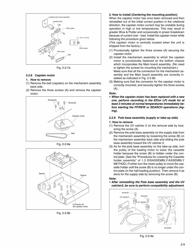
2.2.7 Loading motor
1. How to remove(1) Remove the belt wound around the worm gear.(2) Open the two lugs of the motor guide and remove the
loading motor, loading motor board assembly and motorguide altogether by pulling them up.
(3) When replacing the loading motor board assembly, takecare with the orientation of the loading motor. (Install sothat the loading motor label faces upward.)
(4) When the motor pulley has been replaced, choose thefitting dimension as indicated in Fig.2-2-7a.
2.2.4 Pinch roller arm assembly
1. How to remove(1) Remove the spring from the hook of the press lever as-
sembly.(2) Remove the slit washer and remove the pinch roller seat
2. (See Fig.2-2-4a.)(3) Remove the pinch roller arm assembly by pulling it up.
Fig. 2-2-5a
2.2.6 A/C head
1. How to remove(1) Remove the two screws (A) and remove the A/C head
together with the head base.(2) When replacing only the A/C head, remove the three
screws (B) while controlling the compression spring.
Fig. 2-2-6a
Fig. 2-2-6c
Fig. 2-2-4a
2.2.5 Guide arm assembly and press lever assembly
1. How to remove(1) Remove the spring and expand the lug of the lid guide in
the arrow-indicated direction. Then remove the guide armassembly by pulling it up.
(2) Remove the press lever assembly by pulling it up. (SeeFig.2-2-5a.)
Tension spring
Press lever assembly
Guide arm assembly
LugLid guide
Head base
Screws(A)
A/C head
Compression springs
Head base
A/C head boardassembly
A/C head
Screws(B)
Fig. 2-2-6b
2. How to install(1) To make the post-installation adjustment easier, set the
temporary level as indicated in Fig.2-2-6c. Also make surethat the screw center (centre) is brought into alignmentwith the center (centre) position of the slot.
Head base
Head base
Screw
A/C head
A/C head
12.4 mm
Pinch roller seat2
Pinch roller arm assembly
Pinch roller arm assembly
Slit washer
Spring
Press lever assembly
Fig. 2-2-3i
Relay gear
Drive gear Limit gear
Guide holeNotches Notch
B
AA
B
2-9
Fig. 2-2-8b
Loading motor board assembly
Loading motor
Motor guide
Worm gear
Belt
Lugs
6.5 ± 0.2 mm
Motor pulley
LAB
EL
Fig. 2-2-7a
Fig. 2-2-8a
2.2.8 Capstan motor
1. How to remove(1) Remove the belt (capstan) on the mechanism assembly
back side.(2) Remove the three screws (A) and remove the capstan
motor.
Capstan motor
Belt
Screw(A)
Screws(A)
2. How to install (Centering the mounting position)When the capstan motor has once been removed and thenreinstalled out of the initial correct position in the rotationaldirection, the capstan motor current may be unstable duringoperation in high or low temperatures. This may result ingreater Wow & Flutter and occasionally in power breakdownbecause of current over - load. Install the capstan motor whilefollowing the procedure given below.(The capstan motor is centrally located when the unit isshipped from the factory.)
(1) Provisionally tighten the three screws (A) securing thecapstan motor.
(2) Install the mechanism assembly to which the capstanmotor is provisionally fastened on the bottom chassiswhich incorporates the Main board assembly. (No needto tighten the screws for mounting the mechanism.)Make sure that all the connectors for the mechanism as-sembly and the Main board assembly are correctly in-stalled as indicated in Fig. 2-2-8b.
(3) Making sure that the connector for the capstan motor iscorrectly mounted, and securely tighten the three screws(A).
Note:• When the capstan motor has been replaced with a new
one, perform recording in the EP(or LP) mode for atleast 2 minutes at normal temperatures immediately be-fore starting the FF/REW or SEARCH operations (Ag-ing).
SpacerSpacer
Connector forthe capstan motor
2.2.9 Pole base assembly (supply or take-up side)
1. How to remove(1) Remove the UV catcher 2 on the removal side by loos-
ening the screw (A).(2) Remove the pole base assembly on the supply side from
the mechanism assembly by loosening the screw (B) onthe mechanism assembly back side and sliding the polebase assembly toward the UV catcher 2.
(3) As for the pole base assembly on the take-up side, turnthe pulley of the loading motor to lower the cassetteholder because the screw (B) is hidden under the con-trol plate. (See the “Procedures for Lowering the Cassetteholder assembly” of 1.3 DISASSEMBLY/ASSEMBLYMETHOD.) Further turn the motor pulley to move the cas-sette holder until the screw (B) is no longer under the con-trol plate (in the half-loading position). Then remove it asdone for the supply side by removing the screw (B).
Note:• After reinstalling the Pole base assembly and the UV
catcher2, be sure to perform compatibility adjustment.
Fig. 2-2-9a
Screw(B)
Screw(A)
UV catcher2
Screw(A)
UV catcher2

2-10
Fig. 2-2-11a
2. How to install(1) Install the clutch gear, spring (A), spring (C), direct gear,
spacer and others to the individual shafts of the maindeck, and finally the slit washer. (See Fig.2-2-12a.)
(2) Let the spring (B) drops into the rotary encoder guide holeand install the change lever assembly.(Take care not tomistake a direction of the spring.) The point is to slightlylift the coupling gear and catch it from the both sides withthe assembly. (See Fig.2-2-12b.)
Slit washer
Belt
Clutch unit
2.2.11 Clutch unit
(1) Remove the belt wound around the capstan motor andthe clutch unit.
(2) Remove the slit washer and remove the clutch unit.
Fig. 2-2-12b
Fig. 2-2-12a
Spacer
Change lever assembly
Direct gear
Clutch gear
Spring (C)
Slit washer
Lugs
Spring(A)Position the projecting side down.
Spring(B)
Washer (*1)
Spacer
Coupling gear
Spring(B)
Rotary encoder guide
Main deck Main deck
Change lever assembly
Coupling gear
2.2.12 Change lever assembly, direct gear, clutch gearand coupling gear
1. How to remove(1) Release the two lugs of the rotary encoder guide in the
arrow-indicated direction and remove the change leverassembly.
(2) Remove the slit washer retaining the direct gear and re-move the latter.Take care so as not to lose the washer and spring. (SeeFig.2-2-12a.)
2.2.10 Rotary encoder
1. How to remove(1) Remove the screw (A) and remove the rotary encoder
by pulling it up. (See Fig. 2-2-10a.)
Fig. 2-2-10a
Rotary encoder (Front side)
Screw(A)
Rotary encoder (Back side)
Positioning pin of the rotary encoder
Guide marks
Fig. 2-2-10b
2. How to install (Phase matching)(1) Make sure that the mark E of the control plate is in align-
ment with the mark of the loading arm gear shaft andbring the guide marks on the rotary encoder into align-ment as indicated in Fig.2-2-10a. (See Fig. 2-2-10a andFig. 2-2-10b.)
(2) Turn over the rotary encoder with its guide marks kept inalignment and install it by fitting on the shaft of the rotaryencoder guide and the positioning pin.
(3) Tighten the screw (A) to complete the installation.
Control plateShaft of the rotary encoder guide
Mark E
Note:• The parts with marked (*) have different types of mechanisms (standard type or high-
speed FF/REW type).
*1 : Uses the standard type mechanism only.
*2 : Uses the high-speed FF/REW type mechanism only.
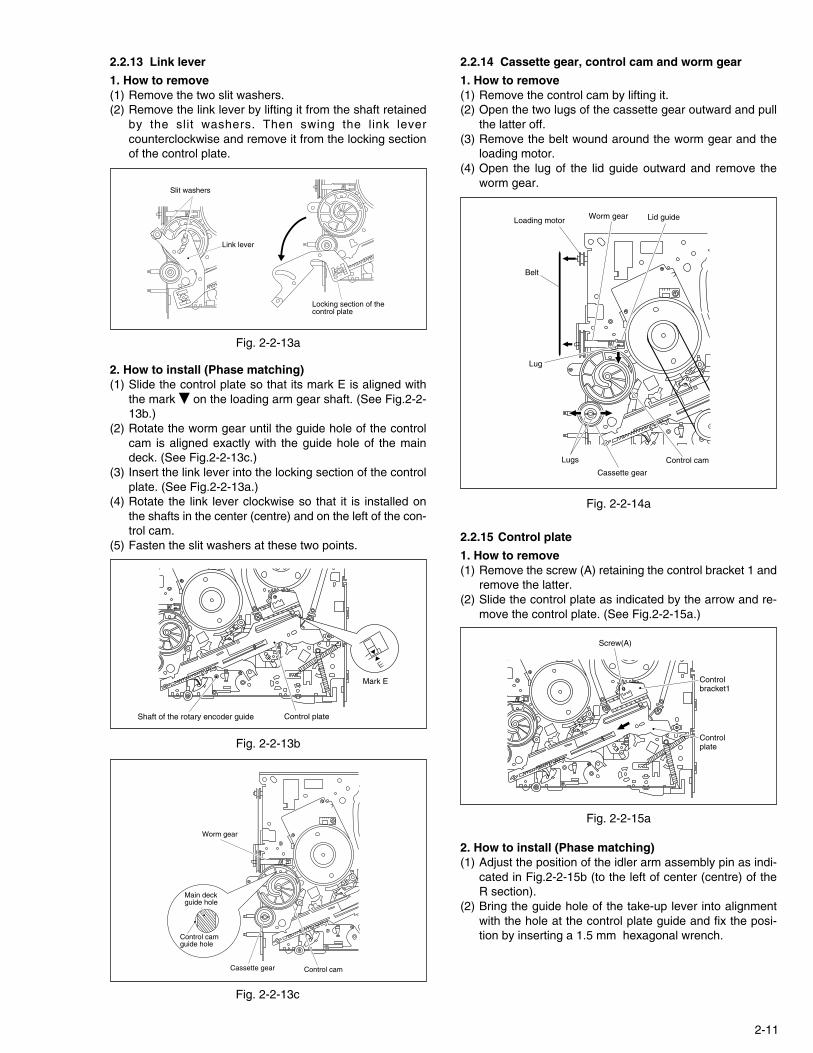
2-11
Fig. 2-2-13a
Slit washers
Link lever
Locking section of the control plate
2.2.13 Link lever
1. How to remove(1) Remove the two slit washers.(2) Remove the link lever by lifting it from the shaft retained
by the slit washers. Then swing the link levercounterclockwise and remove it from the locking sectionof the control plate.
Fig. 2-2-13b
2. How to install (Phase matching)(1) Slide the control plate so that its mark E is aligned with
the mark on the loading arm gear shaft. (See Fig.2-2-13b.)
(2) Rotate the worm gear until the guide hole of the controlcam is aligned exactly with the guide hole of the maindeck. (See Fig.2-2-13c.)
(3) Insert the link lever into the locking section of the controlplate. (See Fig.2-2-13a.)
(4) Rotate the link lever clockwise so that it is installed onthe shafts in the center (centre) and on the left of the con-trol cam.
(5) Fasten the slit washers at these two points.
Control plateShaft of the rotary encoder guide
Mark E
Fig. 2-2-13c
Worm gear
Control cam
Main deck guide hole
Control cam guide hole
Cassette gear
2.2.14 Cassette gear, control cam and worm gear
1. How to remove(1) Remove the control cam by lifting it.(2) Open the two lugs of the cassette gear outward and pull
the latter off.(3) Remove the belt wound around the worm gear and the
loading motor.(4) Open the lug of the lid guide outward and remove the
worm gear.
Fig. 2-2-14a
2.2.15 Control plate
1. How to remove(1) Remove the screw (A) retaining the control bracket 1 and
remove the latter.(2) Slide the control plate as indicated by the arrow and re-
move the control plate. (See Fig.2-2-15a.)
Belt
Loading motor
Lug
Worm gear Lid guide
Lugs
Cassette gear
Control cam
Fig. 2-2-15a
Control bracket1
Control plate
Screw(A)
2. How to install (Phase matching)(1) Adjust the position of the idler arm assembly pin as indi-
cated in Fig.2-2-15b (to the left of center (centre) of theR section).
(2) Bring the guide hole of the take-up lever into alignmentwith the hole at the control plate guide and fix the posi-tion by inserting a 1.5 mm hexagonal wrench.

2-12
2. How to install(1) Align the notch of the loading arm gear (take-up side) to
the projection B of the loading arm gear shaft and slip itover. Then rotate it clockwise for alignment with the pro-jection A and slip it down to the bottom. (See Fig.2-2-16b.)
(2) Then turn the loading arm gear (take-up side)counterclockwise. Hang the torsion arm on the pole baseassembly (take-up side) and tighten the screw (B).
(3) Install the loading arm gear (supply side) so that the guidemark of the loading arm gear (take-up side) is in align-ment with the guide mark of the loading arm gear (sup-ply side). Then hang the torsion arm on the pole baseassembly (supply side) and tighten the screw (A). (SeeFig.2-2-16a.)
Fig. 2-2-16b
Projection A Loading arm gear shaft
Loading arm gear (take-up side)
Projection B
Fig. 2-2-15b
Idler arm assembly pin
Take-up lever
Insert
R section
Guide hole of the control plate guide
1.5mm hexagonal wrench
2.2.16 Loading arm gear (supply or take-up side) andloading arm gear shaft
1. How to remove(1) Remove the loading arm gear (supply side) by loosen-
ing the screw (A). (See Fig. 2-2-16a.)(2) Remove the screw (B) and remove the torsion arm from
the pole base assembly (take-up side). (See Fig.2-2-16a.)
Fig. 2-2-15c
Section AHole A
Section BHole B
Section CControl plate
Pole base assembly (supply side)
Press-fit
Section B
Hole BSection C Tension arm assembly shaft
Section DSection D
Section A
Hole A
(3) Install the control plate so that the section A of the load-ing arm gear shaft fits into the hole (A) of the control plate,the section B of the control plate guide into the hole (B),and the control plate comes under the section C of therotary encoder guide and the section D of the loading armgear shaft while press-fit the pole base assmebly (sup-ply side) as indicated by the arrow. It is important thatthe tension arm assembly shaft is positioned closer to-ward you than the control plate. (See Fig.2-2-15c.)
(4) Make sure that the mark E of the control plate is in align-ment with the mark of the loading arm gear shaft. (SeeFig.2-2-15c.)
(5) Pull off the hexagonal wrench for positioning.
Fig. 2-2-16a
(3) Turn the loading arm gear (take-up side) clockwise sothat the notch of the loading arm gear (take-up side) isin alignment with the projection of the loading arm gearshaft and lift it.Likewise, turn the loading arm counterclockwise so thatthe notch is in alignment with the projection and removethe loading arm gear (take-up side). (See Fig.2-2-16a andFig. 2-2-16b.)
(4) When removing the loading arm gear shaft, be sure offirst removing the screw retaining the drum assembly (onthe back side of the loading arm gear shaft). Then re-move the screw (C) and remove the loading arm gearshaft by sliding it.
Guide marks
Screw(A)
Screw(C)
Notch
Pole base assembly(supply side)
Pole base assembly(take-up side)
Screw(B)
Torsion arm
Loading arm gear(take-up side)
Loading arm gear(supply side) Loading arm gear shaft

2-13
2.2.17 Take-up lever, take-up head and control plateguide
(1) Remove the spring of the take-up lever from the maindeck.
(2) Remove the lug (A) of the take-up lever from the maindeck and pull out the take-up lever and the take-up headtogether.
(3) Remove the screw (A).(4) Align the idler arm assembly pin in the center (centre) of
the R section of the control plate guide, remove the con-trol plate guide lugs (B) and (C) from the main deck, andremove the control plate guide.
Fig. 2-2-17a
Take-up head
Screw(A)
Lug(A)
Lug(B)
Control plate guide
Take-up lever
Lug(C)
Idler arm assembly pin
2.2.18 Capstan brake assembly
1. How to remove(1) Move the lug (A) of the capstan brake assembly in the
arrow-indicated direction so that it comes into alignmentwith the notch of the main deck. (See Fig. 2-2-18a.)
(2) Remove the lug (B) of the capstan brake assembly fromthe main deck and remove the capstan brake assembly.
Fig. 2-2-18a
Capstan brake assembly
Lug(A)
Lug(B)
2.2.19 Sub brake assembly (take-up side)
1. How to remove(1) Remove the spring attached to the lid guide and sub
brake assembly (take-up side).(2) Bring the lug (A) of the sub brake assembly (take-up side)
into alignment with the notch of the main deck.(3) Remove the lugs (B) and (C) of the sub brake assembly
(take-up side) from the main deck and remove the subbrake assembly (take-up side).
Fig. 2-2-19a
Spring
Sub brakeassembly(take-up side)
Lug(B)
Lug(A)
Lug(C)
Fig. 2-2-20a
Lug(D)
Lug(C) SpringLug(E)
Lug(A)
Lug(B)
Main brake assembly(take-up side)
Reel disk(take-up side)
Main brake assembly(supply side)
Notch
2.2.20 Main brake assembly (take-up side), reel disk(take-up side) and main brake assembly (supplyside)
1. How to remove(1) Move the main brake assembly (take-up side) in the ar-
row-indicated direction and remove the reel disk (take-up side).
(2) Remove the spring attached to the main brake assembly.(3) Remove the lug (A) of the main brake assembly (take-
up side) and pull out the lug (B) after bringing it into align-ment with the main deck notch.
(4) Remove the lugs (C), (D) and (E) of the main brake as-sembly (supply side) from the main deck and pull themoff. (See Fig.2-2-20a.)
(5) When installing the main brake assembly (take-up side),slide the brake lever in the direction as indicated by thearrow to prevent it from hitting the projection of the mainbrake assembly (take-up side). (See Fig.2-2-20b.)
Fig. 2-2-20b
Projection of the mainbrake assembly(take-up side)
Rotary encoder guide(*1)Brakelever
Note:• The parts with marked ( *) have different types of mechanisms (standard type
or high-speed FF/REW type).
*1 : Uses the standard type mechanism only.

2-14
2.2.22 Idler lever, idler arm assembly
1. How to remove(1) Remove the lug of the idler lever from the main deck and
remove the hook fitted in the idler arm assembly hole bylifting it.
(2) Remove the slit washer and pull out the idler arm assem-bly.
2.2.24 Rotor assembly
1. How to remove(1) Remove the stator assembly.(2) Remove the two screws (B) and remove the rotor assem-
bly.
2. How to install(1) Match the phases of the upper drum assembly and the
rotor assembly as indicated in Fig.2-2-24a.(2) Place the upper drum assembly hole (a) over the rotor
assembly holes (b) (with three holes to be aligned) andtighten the two screws (B). (See Fig.2-2-24a.)
Lug Idler lever
Hook
Idler armassembly
Slit washer
Fig. 2-2-23a
Stator assembly Flat cable(Take care not to mix up thepolar faces when installing.)
Lug wire(Note)
Screw (A)
Screw (A)
Lug wire
Drumshaft
Screw (B)
2.2.21 Tension brake assembly, reel disk (supply side)and tension arm assembly
1. How to remove(1) Remove the three lugs of the tension brake assembly
from the main deck and pull them off.(2) Remove the reel disk (supply side) by loosening in the
arrow-indicated direction the main brake assembly (sup-ply side).
(3) Remove the tension spring on the back of the main deck.Then release the lug of the tension arm bearing in thearrow-indicated direction and draw out the tension armassembly. (See Fig. 2-2-21a.)
Fig. 2-2-21a
Lugs
Tension brakeassembly
Lug of the tensionarm bearing
Reel disk(supply side)
Tension armassembly
Tension spring Main brake assembly(supply side)
Fig. 2-2-22a
Screws (B)
Rotor assembly
Hole(a)
Hole(b)
Screw holes
Upper drumassembly
The hole is not in line but is offset toward the right.
Fig. 2-2-24a
2.2.23 Stator assembly(1) Remove the flat cable.(2) Remove the two screws (A), (B) and remove the lug wire.(3) Remove the stator assembly by lifting in the arrow-indi-
cated direction. (Take care that the brush spring does notjump out.)
Notes:• Be careful not to lose the brush and spring.• There are some models that do not use the lug wire.
Refer to the parts list for these models.• When tightening the screw (B), place the caulked part
of the lug terminal near to the shaft of the drum andthen tighten it.
• After installation, be sure to perform the switchingpoint adjustment according to the electrical adjustmentprocedure.

2-15
2.2.25 Upper drum assembly
Notes:• To replace the upper drum assembly only may not be
possible with some models. For upper drum assem-bly replacement, refer to the parts list. (When the partsnumber of the upper drum assembly is not listed onthe parts list, then this cannot be replaced.)
• When replacement is required, control the up- downmovement of the brush. Never apply grease.
• When replacing the upper drum assembly, replace itthe together with the washer.
1. How to remove(1) Remove the stator assembly and rotor assembly.(2) Loosen the screw of the collar assembly using a 1.5 mm
hexagonal wrench and remove the collar assembly. Alsoremove the brush, spring and cap at one time.
(3) Remove the upper drum assembly and remove thewasher using tweezers.
2. How to install(1) Clean the coil parts of the lower drum assembly and the
newly installed upper drum assembly with an air brushin advance. (See Fig.2-2-25b.)
(2) Install a new washer and upper drum assembly on thedrum shaft. (See Fig.2-2-25a.)
(3) Install the cap to the upper drum assembly.(4) Position the collar assembly as indicated in Fig.2-2-25c
while controlling its up- down movement.(5) Secure the collar assembly in position with a hexagonal
wrench while pressing its top with the fingers.(6) After installation, gently turn the upper drum assembly
with your hand to make sure that it turns normally. Theninstall the brush and the spring.
(7) Install the rotor assembly and stator assembly accordingto Fig 2-2-23a and 2-2-24a.
(8) When installation is complete, clean the upper drum as-sembly and lower drum assembly and carry out the fol-lowing adjustments.
• PB switching point adjustment• Slow tracking adjustment• Compatibility adjustment (Be sure to check for compat-
ibility for the EP (or LP) mode.)
Fig. 2-2-25a
Fig. 2-2-25b
Spring
Brush
Cap
Upper drumassembly
Washer
Lower drum assembly
Shaft
1.5 mm hexagonal wrench
Loosen
Collarassembly
Upper drum assembly
Coil parts
Lower drum assembly
Fig. 2-2-25c
Fig. 2-2-25d
CollarassemblyUpper drum
assembly
TightenCollarassembly
Press

2-16
Fig. 2-3-1a
Improper waveform variation
Max level Min level Proper waveform variation
Fig. 2-3-1b
Roller driver
Guide roller (supply side)
2.3 Compatibility adjustment
Notes:• Although compatibility adjustment is very important,
it is not necessary to perform this as part of the nor-mal servicing work. It will be required when you havereplaced the A/C head, drum assembly or any part ofthe tape transport system.
• To avoid any damage to the alignment tape while per-forming the compatibility adjustment, get a separatecassette tape (for recording and play back) ready tobe used for checking the initial tape running behavior.
• Unless otherwise specified, all measuring points andadjustment parts are located on the Main board.
• When using the Jig RCU, it is required to set the VCRto the Jig RCU mode (the mode in which codes fromthe Jig RCU can be received). (See SECTION 1 DISAS-SEMBLY.)
(1) Play back the alignment tape (A1).(2) Apply the external trigger signal to D.FF (E), to observe
the V.PB FM waveform at the measuring point (D).(3) Set the VCR to the manual tracking mode.(4) Make sure that there is no significant level drop of the
V.PB FM waveform caused by the tracking operation, withits generally parallel and linear variation ensured. Per-form the following adjustments when required. (See Fig.2-3-1a.)
(5) Reduce the V.PB FM waveform by the tracking opera-tion. If a drop in level is found on the left side, turn theguide roller of the pole base assembly (supply side) withthe roller driver to make the V.PB FM waveform linear.If a drop in level is on the right side, likewise turn the guideroller of the pole base assembly (take-up side) with theroller driver to make it linear. (See Fig. 2-3-1c.)
(6) Make sure that the V.PB FM waveform varies in paralleland linearly with the tracking operation again. When re-quired, perform fine-adjustment of the guide roller of thepole base assembly (supply or take-up side).
2.3.1 FM waveform linearity
Fig. 2-3a Jig RCU [PTU94023B]
(7) Unload the cassette tape once, play back the alignmenttape (A1) again and confirm the V.PB FM waveform.
(8) After adjustment, confirm that the tape wrinkling does notoccur at the roller upper or lower limits. (See Fig. 2-3-1d.)
[Perform adjustment step (9) only for the modelsequipped with SP mode and EP (or LP) mode.]
(9) Repeat steps (1) to (8) by using the alignment tape (A2).
INITIAL MODE
DATA CODE
CUSTOM CODE43: A CODE
[Data transmitting method]Depress the “ ” ( 3 ) button after the data code is set.
Jig RCU
Signal (A1) • Alignment tape(SP, stairstep, PAL) [MHPE](A2) • Alignment tape(LP, stairstep, PAL) [MHPE-L]
Mode (B) • PB
Equipment (C) • Oscilloscope
Measuring point (D) • TP106 (PB. FM)
External trigger (E) • TP111 (D.FF)
Adjustment part (F) • Guide roller [Mechanism assembly]
Specified value (G) • Flat V.PB FM waveform
Adjustment tool (H) • Roller driver [PTU94002]

2-17
Fig. 2-3-1d
(a) Guide roller
(b) Guide pole
Improper Proper
Fig. 2-3-1c
A B
C D
Level drop at the guide roller (supply side)
Level drop at the guide roller (take-up side)
• Proper waveform variation: Always flat
• Improper waveform variation:
Higher Lower
2.3.2 Height and tilt of the A/C head
Note:• Set a temporary level of the height of the A/C head in
advance to make the adjustment easier after the A/Chead has been replaced. (See Fig.2-2-6c.)
(2)
(3)
(1)
AUDIO OUT
Head base
A/C head
CTL. P
Fig. 2-3-2a
(1) Play back the alignment tape (A).(2) Apply the external trigger signal to D.FF (E), to observe
the AUDIO OUT waveform and Control pulse waveformat the measuring points (D1) and (D2) in the ALT mode.
(3) Set the VCR to the manual tracking mode.
Signal (A) • Alignment tape(SP, stairstep, PAL) [MHPE]
Mode (B) • PB
Equipment (C) • Oscilloscope
Measuring point (D1) • AUDIO OUT terminal(D2) • TP4001 (CTL. P)
External trigger (E) • TP111 (D.FF)
Adjustment part (F) • A/C head [Mechanism assembly]
Specified value (G) • Maximum waveform
2.3.3 A/C head phase (X-value)
Signal (A1) • Alignment tape(SP, stairstep, PAL) [MHPE]
Mode (B) • PB
Equipment (C) • Oscilloscope
Measuring point (D) • TP106 (PB. FM)
External trigger (E) • TP111 (D.FF)
Adjustment part (F) • A/C head base [Mechanism assembly]
Specified value (G) • Maximum V.PB FM waveform
Adjustment tool (H) • A/C head positioning tool [PTU94010]
(1) Play back the alignment tape (A1).(2) Apply the external trigger signal to D.FF (E), to observe
the V.PB FM waveform at the measuring point (D).(3) Set the VCR to the manual tracking mode.(4) Loosen the screws (4) and (5), then set the A/C head
positioning tool to the innermost projected part of the A/C head. (See Fig. 2-3-3a.)
(5) Turn the A/C head positioning tool fully toward the cap-stan. Then turn it back gradually toward the drum andstop on the second peak point position of the V.PB FMwaveform output level. Then tighten the screws (4) and(5).
(6) Perform the tracking operation and make sure that theV.PB FM waveform is at its maximum.If it is not at maximum, loosen the screws (4) and (5),and turn the A/C head positioning tool to bring the A/Chead to a position, around where the waveform reachesits maximum for the first time. Then tighten the screws(4) and (5).
(4) Adjust the AUDIO OUT waveform and Control pulsewaveform by turning the screws (1), (2) and (3) little bylittle until both waveforms reach maximum. The screw (1)and (3) are for adjustment of tilt and the screw (2) for azi-muth.

2-18
2.3.4 Standard tracking preset
Fig. 2-3-3b
Fig. 2-3-3a
Alignment tape [SP, stairstep]played with the SP head
Alignment tape [EP(LP), stairstep]played with the EP(LP) head
Drum side Control head position Capstan side
X-value adjustment point
Maximum
Wav
efor
m o
utpu
t[Perform adjustment steps (7) to (10) only for 2 Headmodels equipped with LP mode.]
(7) Then play back the alignment tape (A2).(8) Set the VCR to the manual tracking mode.(9) Perform the tracking operation and make sure that the
V.PB FM waveform is at its maximum.(10) If it is not at maximum, loosen the screws (4) and (5),
and turn the A/C head positioning tool to bring the A/Chead to a position, around where the waveform reachesits maximum for the first time. Then tighten the screws(4) and (5).
Note:• After adjusting, always perform the confirmation and
re-adjustment of the item 2.3.4.
(1) Play back the alignment tape (A).(2) Apply the external trigger signal to D.FF (E), to observe
the V.PB FM waveform at the measuring point (D).(3) Confirm that the automatic tracking operation is com-
pleted.
Signal (A) • Alignment tape(LP, stairstep, PAL) [MHPE-L]
Mode (B) • PB ¥ Auto adjust
Equipment (C) • Oscilloscope
Measuring point (D) • TP106 (PB. FM)
External trigger (E) • TP111 (D.FF)
Adjustment part (F) • Jig RCU: Code “50”
Specified value (G) • STOP mode(Maximum V.PB FM waveform)
Adjustment tool (H) • Jig RCU [PTU94023B]
2.3.5 Tension pole position
(1) Play back the back tension cassette gauge (A).(2) Check that the indicated value on the left side gauge is
within the specified value (G).(3) If the indicated value is not within the specified value (G),
perform the adjustment in a following procedure.
1) Set the VCR to the mechanism service mode. (SeeSECTION 1 DISASSEMBLY.)
2) Set the VCR to the play back mode and adjust by turn-ing adjustment pin to align the tension arm assemblyedge with the main deck hole (A) on the right edgemarker. (See Fig. 2-3-5a)
Signal (A) • Back tension cassette gauge[PUJ48076-2]
Mode (B) • PB
Adjustment part (F) • Adjust pin [Mechansim assembly]
Specified value (G) • 25 - 51 gf•cm (2.45 – 5 × 10⁻³ Nm]
0.5 mm
Hole (A)Edge
Marker
Tension armassembly
Adjust pin
Tension brake assembly
Tension arm assembly
A/C head positioning tool Screw (4)
Screw (5)
Toward the drumToward the capstan
To the drum
A/C headTo the capstan
Head base
Fig. 2-3-5a
(4) Set the VCR to the Auto adjust mode by transmitting thecode (F) twice from the Jig RCU. When the VCR entersthe stop mode, the adjustment is completed.
(5) If the VCR enters the eject mode, perform adjustment forthe audio control head phase (X-value) again.

2-19
Control plate mark E U CI
CASS-INS
FR
FF/REW
ST
STOP
R
REV
SL
SLOW/STILL
P
PLAYEJECT END
CASS-UPMechanism mode
HIGH
LOWC CH
Rotary encoderHIGH
LOWB CH
HIGH
ONHALF PRESS
CONTACTOFF
LOWA CH
0Control cam angle 69 136 370 412.42318.7264.7230
0Rotary encoderangle
Pole base
20 42.6 52.6 114.6 150.4 167.8 178.8 207.2 218.2 240.2 251.2 293.2 304.2 320.4 335
IN FF/REW
OUT PLAY
Direct gear
Change lever 2
ONHALF REV
HALF FF/REWOFF
Tension arm
ONCONTACT
OFF
Main brake S
ONCONTACT
OFF
Main brake T
ON
OFF
Sub brake S
ON
OFF
Sub brake T
ON
OFF
OFF
ON
Capstan brake
ON
OFF
Rec safety switch
Operation mode
ON PLAYON REV
CONTACTOFF
(C-INS)
Pinch roller
SUPPLY
CENTER
TAKE-UP
Idler position
READY
RESET
Take-up lever
ON
OFF
Guide arm
Timer RECstandby
Backspace Slow FOR
STOP(drum at stop)
Search REW REC
REC pause
POWER OFF(cassette loaded)
Slow REW Search FF
STOP(drum in motion)
Mechanism Timing Chart

3-1
SECTION 3ELECTRICAL ADJUSTMENT
3.1 Precaution
The following adjustment procedures are not only necessaryafter replacement of consumable mechanical parts or boardassemblies, but are also provided as references to be referredto when servicing the electrical circuitry.In case of trouble with the electrical circuitry, always begin aservice by identifying the defective points by using the meas-uring instruments as described in the following electrical ad-justment procedures. After this, proceed to the repair, replace-ment and/or adjustment. If the required measuring instrumentsare not available in the field, do not change the adjustmentparts (variable resistor, etc.) carelessly.
3.1.1 Required test equipments
• Color (colour) television or monitor• Oscilloscope: wide-band, dual-trace, triggered delayed sweep• Frequency counter• Signal generator: RF / IF sweep / marker• Signal generator: stairstep, color (colour) bar [PAL/SECAM]• Recording tape• Digit-key remote controller (provided)
3.1.2 Required adjustment tools
3.1.3 Color (colour) bar signal,Color (colour) bar pattern
3.1.4 Switch settings and standard precautions
The SW settings of the VCR and the standard precautions forthe electrical adjustments are as follows.
• When using the Jig RCU, it is required to set the VCR tothe Jig RCU mode (the mode in which codes from the JigRCU can be received). (See SECTION 1 DISASSEMBLY.)
0.3 Vp-p
0.7 Vp-p
R-Y B-Y R-Y B-YCyan
Carrier(4.250 MHz) Horizontal sync
Blu
eR
edM
agen
taG
reenW
hite
(100
%)
Yel
low
Whi
te(1
00%
)
Carrier(4.406 MHz)
B-Y colour BARR-Y colour BAR
Whi
te
Yel
low
Cya
n
Gre
en
Mag
enta
Red
Blu
e
B–Y BlackWhite100%R–Y
s Colour bar signal [SECAM] s Colour bar pattern [SECAM]
Jig RCUPTU94023B
Alignment tape(SP, stairstep, PAL)
MHPE
Alignment tape(LP, stairstep, PAL)
MHPE-L
LPFPTU93006
Alignment tape(S-VHS, SP/LP, color (colour) bar)
MH-2H3.1.5 EVR Adjustment
Some of the electrical adjustments require the adjustmentperformed by the EVR system. The main unit have EEPROMsfor storing the EVR adjustment data and user setups.
Notes:• In the EVR adjustment mode, the value is varied with
the channel buttons (+, –). The adjusted data is storedwhen the setting mode changes (from PB to STOP,when the tape speed is changed, etc.). Take care toidentify the current mode of each adjustment itemwhen making an adjustment.
• When changing the address setting in the EVR adjust-ment mode, use the Jig RCU or the remote controllerhaving numeric keypad with which a numeric code canbe directly input.The remote control code of the Jig RCU correspondsto each of the digit keys on the remote controller asfollows.
• As the counter indication and remaining tape indica-tion are not displayed FDP during the EVR adjustmentmode, check them on the TV monitor screen.
• When performing the EVR adjustment, confirm that theFDP indication is changed to the EVR mode, as shownbelow.
Digit-key 0 1 2 3 4 5 6 7 8 9
Code 20 21 22 23 24 25 26 27 28 29
• Set the switches as shown below unless otherwisespecified on the relevant adjustment chart. The switchesthat are not listed below can be set as desired.If the VCR is not equipped with the functions detailedbelow, setup is not required.
• If there is a reference to a signal input methed in thesignal column of the adjustment chart, “Ext. S-input”means the Y/C separated video signal and “Ext. input”means the composite video signal input.
• Unless otherwise specified, all measuring points andadjustment parts are located on the Main board.
INITIAL MODE
DATA CODE
CUSTOM CODE43: A CODE
[Data transmitting method]Depress the “ ” ( 3 ) button after the data code is set.
Jig RCU
AUTO PICTURE/VIDEO CALIBRATION/ OFFB.E.S.T./D.S.P.C.
PICTURE CONTROL/SMART PICTURE NORMAL/NATURAL
VIDEO STABILIZER OFF
TBC ON
Digital 3R ON
VIDEO NAVIGATION/TAPE MANAGER OFF
FDP
Fig. 3-1-4a Jig RCU [PTU94023B]
Fig. 3-1-5a EVR mode
(75%)
White(75%)
0.7 V
0.3 V
Horizontal sync
V U
1V
White(100%)
Yel
low
Cya
nG
reen
Mag
enta
Red
Blu
e
Burst
0.3 V
V(R-Y)U(B-Y)
Whi
te
Yel
low
Cya
n
Gre
en
Mag
enta
Red
Blu
e
U BlackWhite100%V
• Color(colour) bar signal [PAL] • Color(colour) bar pattern [PAL]

3-2
Fig. 3-2-1a Switching point
V.syncTrigger pointSwitching point
V. rate
3.2.2 Slow tracking preset
Signal (A1) • Ext. input(A2) • Color (colour) bar signal [PAL]
Mode (B1) • VHS SP(B2) • VHS LP
Measuring point (D) • TV-Monitor
Adjustment part (F) • Jig code “71“ or “72”
Specified value (G) • Minimum noise
Adjustment tool (H) • Jig RCU [PTU94023B]
(1) Record the signal (A2) in the mode (B1), and play backthe recorded signal.
(2) Set the VCR to the manual tracking mode.(3) Set the VCR to the FWD slow (+1/6x) mode.(4) Transmit the code (F) from the Jig RCU to adjust so that
the noise bar becomes the specified value (G) on the TVmonitor in the slow mode.
(5) Set the VCR to the Stop mode.(6) Confirm that the noise bar is (G) on the TV monitor in
the slow mode.(7) Repeat steps (3) to (6) in the REV slow (–1/6x) mode.(8) Repeat steps (1) to (7) in the mode (B2).
Note:• For FWD slow (+1/6x) playback, transmit the code “08”
from the Jig RCU to enter the slow playback mode, andtransmit the code “D0” for REV slow (–1/6x) mode.
3.2 Servo circuit
3.2.1 Switching point
Signal (A1) • Stairstep signal(A2) • Alignment tape (SP,stairstep,PAL) MHPE
Mode (B) • PB
Equipment (C) • Oscilloscope
Measuring point (D1) • VIDEO OUT terminal (75Ø terminated)(D2) • TP106 (PB. FM)
External trigger (E) • TP111 (D.FF)/slope : –
Adjustment part (F) • Jig code “5A”
Specified value (G) • 7.5 ± 0.5H
Adjustment tool (H) • Jig RCU [PTU94023B]
(1) Play back the signal (A1) of the alignment tape (A2).(2) Apply the external trigger signal to D.FF (E) to observe
the VIDEO OUT waveform and V.PB FM waveform at themeasuring points (D1) and (D2).
(3) Set the VCR to the manual tracking mode.(4) Adjust tracking so that the V.PB FM waveform becomes
maximum.(5) Set the VCR to the Auto adjust mode by transmitting the
code (F) from the Jig RCU. When the VCR enters thestop mode, the adjustment is completed.
(6) If the VCR enters the eject mode, repeat steps (1) to (5)again.
(7) Play back the alignment tape (A2) again, confirm that theswitching point is the specified value (G).
Fig. 3-3-1a D/A level
(1) Insert the cassette tape (A3) to enter the mode (B).(2) Observe the VIDEO OUT waveform at the measuring
point (D).(3) Check the Y level value when the External S-input (Y/C
separated video signal).(4) Switch the input signal to the External input (composite
video signal), and adjust the adjustment part (F) so thatthe Y level becomes the same value observed in step(3).
Note:• The specified value (G) is just a reference value to be
obtained when the External S-Video (Y/C separatedvideo) signal is input. In actual adjustment, set it tothe value observed in step (3).
H. rate
Y level
3.3 Video circuit
3.3.1 D/A level
Signal (A1) • Ext. S-input / Ext. input(A2) • Color (colour) bar signal [PAL](A3) • S-VHS tape
Mode (B) • S-VHS• EE
Equipment (C) • Oscilloscope
Measuring point (D) • Y OUT terminal (75Ø terminated)
Adjustment part (F) • VR1201 (D/A LEVEL ADJ)[2D DIGITAL board]
• VR1401 [D/A LEVEL ADJ][3D DIGITAL/2M board]
Specified value (G) • 1.00 ± 0.015 Vp-p (reference value)(Note)
Signal (A1) • Ext. input(A2) • Color (colour) bar signal [PAL]
Mode (B1) • EE(B2) • S-VHS SP(B3) • VHS SP
Equipment (C) • Oscilloscope
Measuring point (D) • Y OUT terminal (75Ø terminated)
EVR mode (F1) • Jig code “57”EVR address (F2) • A : 11
(F3) • Jig code “21”(F4) • Jig code “18” or “19” (Channel +/-)
Specified value (G) • 1.00 ± 0.05 Vp-p [2D DIGITAL board]• 1.00 ± 0.03 Vp-p [3D DIGITAL/2M board]
Adjustment tool (H) • Jig RCU [PTU94023B]
(1) Observe the Y OUT waveform at the measuring point (D).(2) Set the VCR to the EVR mode by transmitting the code
(F1) from the Jig RCU.(3) Set the EVR address to (F2) by transmitting the code (F3)
from the Jig RCU.
3.3.2 EE Y/PB Y (S-VHS/VHS) level

3-3
Fig. 3-3-2a EE/PB Y level
H. rate
Y level
(4) Transmit the code (F4) from the Jig RCU to adjust so thatthe Y level of the Y OUT waveform becomes the speci-fied value (G).
(5) Release the EVR mode of the VCR by transmitting thecode (F1) from the Jig RCU again. (When the EVR modeis released, the adjusted data is memorized.)
(6) Record the signal (A2) in the mode (B2), and play backthe recorded signal.
(7) Set the VCR to the manual tracking mode.(8) Repeat steps (1) to (5) in the mode (B2).(9) Record the signal (A2) in the mode (B3), and play back
the recorded signal.(10) Set the VCR to the manual tracking mode.(11) Repeat steps (1) to (5) in the mode (B3).
(1) Connect the adjustment tool (H2) to the measuring point(D1).
(2) Apply the external trigger signal to D.FF (E) to observe thePB color (colour) waveform at the measuring point (D2).
(3) Play back the signal (A3) in the mode (B1) of the align-ment tape (A1).
(4) Set the VCR to the manual tracking mode.(5) Adjust tracking so that the PB color (colour) waveform
becomes maximum. Make a note of the higher PB color(colour) level as “B” at this time.
(6) Record the signal (A3) in the mode (B1), and play backthe recorded signal.
Fig. 3-3-3a LPF [PTU93006]
1 kØ 39 µH 180 µH
120 pF 180 pF
PB. FM 629 [kHz]PB COLOR (PB COLOUR)
3.3.3 REC color (colour) level
Signal (A1) • Alignment tape(S-VHS, SP/LP,Color(colour) bar)
(A2) • Ext. input(A3) • Color (colour) bar signal [PAL]
Mode (B1) • S-VHS SP(B2) • S-VHS LP
Equipment (C) • Oscilloscope
Measuring point (D1) • TP106 (PB. FM)(D2) • PB color (colour) output of the LPF
External trigger (E) • TP111 (D.FF)
EVR mode (F1) • Jig code “57”EVR address (F2) • A : 02
(F3) • Jig code “20” and “22”(F4) • Jig code “18” or “19” (Channel +/-)
Specified value (G) [HR-S6850MS/S7850MS/S7851MS]• SP: “B” x 125 ± 5%• LP: “B” x 125 ± 5%[HR-S8850MS]• SP: “B” x 125 ± 3%• LP: “B” x 125 ± 3%
Adjustment tool (H1) • Jig RCU [PTU94023B](H2) • LPF [PTU93006] (See Fig. 3-3-3a.)
Note:• After adjusting, always perform the confirmation and
re-adjustment of the item 3.4.1.
Fig. 3-3-3b REC color (colour) level
V. rate
Specifiedvalue (G)
(7) Set the VCR to the EVR mode by transmitting the code(F1) from the Jig RCU.
(8) Set the EVR address to (F2) by transmitting the code (F3)from the Jig RCU.
(9) Transmit the code (F4) from the Jig RCU to adjust so thatthe higher level channel becomes the specified value (G)of the note "B" level as shown in Fig. 3-3-3b. (Adjust be-fore recording, then confirm it by playing back.)
(10)After adjustment, record the signal (A3) then playing itback again. At this time, confirm that there is no invert-ing phenomenon or noise appearing on the playbackscreen.
(11)Release the EVR mode of the VCR by transmitting thecode (F1) from the Jig RCU again. (When the EVR modeis released, the adjusted data is memorized.)
(12)Repeat steps (3) to (11) in the mode (B2).
3.3.4 Video EQ (Frequency response)
Signal (A1) • Ext. S-input(A2) • Video sweep signal
Mode (B1) • S-VHS SP(B2) • S-VHS LP(B3) • Picture Control / Smart Picture
REC : Normal / NaturalPB : Edit / Distinct
Equipment (C) • Oscilloscope
Measuring point (D1) • Y OUT terminal (75Ø terminated)Frequency marker(D2) • 3 [MHz]
External trigger (E) • TP111 (D.FF)
EVR mode (F1) • Jig code “57”EVR address (F2) • A : 03
(F3) • Jig code “20” and “23”(F4) • Jig code “18” or “19” (Channel +/-)
Specified value (G) • SP: 3.6 ± 0.4 div. (–1 ± 1 dB)• LP: 3.2 ± 0.4 div. (–2 ± 1 dB)
Adjustment tool (H) • Jig RCU [PTU94023B]
(1) Apply the external trigger signal to D.FF (E) to observethe Y OUT waveform at the measuring point (D1).
(2) Record the signal (A2) in the mode (B1), and play backthe recorded signal.
(3) Set the VCR to the manual tracking mode.(4) Set the VCR to the EVR mode by transmitting the code
(F1) from the Jig RCU.(5) Set the EVR address to (F2) by transmitting the code (F3)
from the Jig RCU.(6) Set the slope of the oscilloscope to the channel having
higher (D2) marker level of the Y OUT waveform [signal(A2)]. Then set the 100 kHz marker level to the “4” scaleon the oscilloscope. In this condition, transmit the code(F4) from the Jig RCU to adjust so that the (D2) markerlevel reaches the specified value (G).
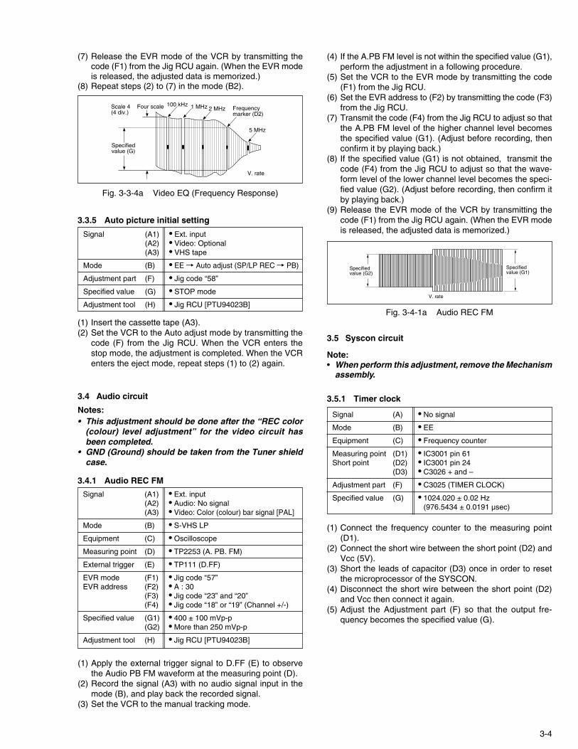
3-4
3.4 Audio circuit
Notes:• This adjustment should be done after the “REC color
(colour) level adjustment” for the video circuit hasbeen completed.
• GND (Ground) should be taken from the Tuner shieldcase.
Signal (A1) • Ext. input(A2) • Audio: No signal(A3) • Video: Color (colour) bar signal [PAL]
Mode (B) • S-VHS LP
Equipment (C) • Oscilloscope
Measuring point (D) • TP2253 (A. PB. FM)
External trigger (E) • TP111 (D.FF)
EVR mode (F1) • Jig code “57”EVR address (F2) • A : 30
(F3) • Jig code “23” and “20”(F4) • Jig code “18” or “19” (Channel +/-)
Specified value (G1) • 400 ± 100 mVp-p(G2) • More than 250 mVp-p
Adjustment tool (H) • Jig RCU [PTU94023B]
(1) Apply the external trigger signal to D.FF (E) to observethe Audio PB FM waveform at the measuring point (D).
(2) Record the signal (A3) with no audio signal input in themode (B), and play back the recorded signal.
(3) Set the VCR to the manual tracking mode.
3.4.1 Audio REC FM
3.3.5 Auto picture initial setting
Signal (A1) • Ext. input(A2) • Video: Optional(A3) • VHS tape
Mode (B) • EE ¥ Auto adjust (SP/LP REC ¥ PB)
Adjustment part (F) • Jig code “58”
Specified value (G) • STOP mode
Adjustment tool (H) • Jig RCU [PTU94023B]
(1) Insert the cassette tape (A3).(2) Set the VCR to the Auto adjust mode by transmitting the
code (F) from the Jig RCU. When the VCR enters thestop mode, the adjustment is completed. When the VCRenters the eject mode, repeat steps (1) to (2) again.
(7) Release the EVR mode of the VCR by transmitting thecode (F1) from the Jig RCU again. (When the EVR modeis released, the adjusted data is memorized.)
(8) Repeat steps (2) to (7) in the mode (B2).
100 kHzFour scale 1 MHz 2 MHz Frequencymarker (D2)
Specifiedvalue (G)
5 MHz
V. rate
Scale 4 (4 div.)
Fig. 3-3-4a Video EQ (Frequency Response)
(4) If the A.PB FM level is not within the specified value (G1),perform the adjustment in a following procedure.
(5) Set the VCR to the EVR mode by transmitting the code(F1) from the Jig RCU.
(6) Set the EVR address to (F2) by transmitting the code (F3)from the Jig RCU.
(7) Transmit the code (F4) from the Jig RCU to adjust so thatthe A.PB FM level of the higher channel level becomesthe specified value (G1). (Adjust before recording, thenconfirm it by playing back.)
(8) If the specified value (G1) is not obtained, transmit thecode (F4) from the Jig RCU to adjust so that the wave-form level of the lower channel level becomes the speci-fied value (G2). (Adjust before recording, then confirm itby playing back.)
(9) Release the EVR mode of the VCR by transmitting thecode (F1) from the Jig RCU again. (When the EVR modeis released, the adjusted data is memorized.)
Fig. 3-4-1a Audio REC FM
V. rate
Specifiedvalue (G1)
Specifiedvalue (G2)
3.5 Syscon circuit
Note:• When perform this adjustment, remove the Mechanism
assembly.
3.5.1 Timer clock
Signal (A) • No signal
Mode (B) • EE
Equipment (C) • Frequency counter
Measuring point (D1) • IC3001 pin 61Short point (D2) • IC3001 pin 24
(D3) • C3026 + and –
Adjustment part (F) • C3025 (TIMER CLOCK)
Specified value (G) • 1024.020 ± 0.02 Hz(976.5434 ± 0.0191 µsec)
(1) Connect the frequency counter to the measuring point(D1).
(2) Connect the short wire between the short point (D2) andVcc (5V).
(3) Short the leads of capacitor (D3) once in order to resetthe microprocessor of the SYSCON.
(4) Disconnect the short wire between the short point (D2)and Vcc then connect it again.
(5) Adjust the Adjustment part (F) so that the output fre-quency becomes the specified value (G).

3-5
3.6 PAL/SECAM Converter circuit
Note:• Unless otherwise specified in this P/S Converter cir-
cuit adjustments, all measuring points and adjustmentparts are located on the P/S Converter board.
Fig. 3-6-2 PAL burst position
Colour burst signal
H-SYNC
H.rate
C(Converted colour)
Y
Specified value (G)
3.6.2 SECAM burst position
(1) Observe the waveforms appeared at the measuringpoints (D1) and (D2).
(2) Adjust the adjustment part (F) so that the waveforms tim-ing width between the H-SYNC and the colour burst sig-nal becomes the specified value (G).
Signal (A1) • Color (colour) bar signal [SECAM]
Mode (B) • EE
Equipment (C) • Oscilloscope
Measuring point (D1) • CN1601 Pin 7(D2) • CN1601 Pin 3
Adjustment part (F) • VR1603
Specified value (G) • T = 5.6 ± 0.1 µsec
3.6.1 Colour difference level
(1) Observe the C (converted colour) waveform at the meas-uring point (D).
(2) Adjust the adjustment part (F1) so that the higher levelof the Yellow and Blue of the C waveform becomes thespecified value (G1).
(3) Adjust the adjustment part (F2) so that the higher levelof the Green and Magenta of the C waveform becomesthe specified value (G2).
Signal (A1) • Color (colour) bar signal [SECAM]
Mode (B) • EE
Equipment (C) • Oscilloscope
Measuring point (D) • CN1601 Pin 7
Adjustment part (F1) • VR1602 (B-Y ADJ)(F2) • VR1601 (R-Y ADJ)
Specified value (G1) • 460 ± 20 mVp-p : VR1602 (B-Y)(G2) • 620 ± 20 mVp-p : VR1601 (R-Y)
GREEN
H.rate
YELLOW BLUE
MAGENTA
Specified value (G2)
Specified value (G1)
Fig. 3-6-1 Colour difference level

4-1
SECTION 4CHARTS AND DIAGRAMS
NOTES OF SCHEMATIC DIAGRAM
Safety precautionsThe Components identified by the symbol arecritical for safety. For continued safety, replace safetycritical components only with manufacturer's recom-mended parts.
1. Units of components on the schematic diagram
Unless otherwise specified.1) All resistance values are in ohm, 1/6 W, 1/8 W (refer to
parts list).Chip resistors are 1/16 W.
K or k: k (1000 ), M: M (1000k )
2) All capacitance values are in µF, (P: PF).3) All inductance values are in µH, (m: mH).4) All diodes are 1SS133, MA165 or 1N4148M (refer to parts
list).
2. Indications of control voltage
AUX : Active at high
AUX or AUX(L) : Active at low
4) Indication on schematic diagramVoltage Indications for REC and PB mode on the sche-matic diagram are as shown below.
Note: If the voltages are not indicated on the schematicdiagram, refer to the voltage charts.
24
C33111/10
22201816
WF25
C3290.1/50
C3300.1/50
R344 47K
R34318K
R34510K
R34615K
Measurement point
Waveform number
5. Waveform measurement
1) Video circuitsREC : Colour bar signal in SP mode, normal VHS modePB : Alignment tape, colour bar SP mode, normal VHS
mode2) Audio circuits
REC : 1KHz, –8 dBs sine wave signal in SP mode, normalVHS mode
PB : REC then playback it3) Movie Camera circuits
Measured using a correctly illuminated gray scale or colourbar test chatrs in the E-E mode
4) Indication on schematic diagramWaveform indications on the schematic diagram are asshown below.
5) Waveform indications
Waveform number
WF25
REC/PB 1.2 Vp-p50 mV/2 msec/DIV
Waveform name ormeasurement point
Level : 1.2 Vp-p
ALC OUT
Mode : REC or PB modes
Oscilloscope Volts and Time/Division, Probe 10 : 1
1 2 32.5
(5.0)1.8
PB and REC modes(Voltage of PB and REC modesare the same)
PB mode
REC mode
3. Interpreting Connector indications
1
2
3
1
2
3
1
2
3
1
4
2
3
Removable connector
Wire soldered directly on board
Non-removable Board connector
Board to Board
Connected pattern on boardThe arrows indicate signal path
4. Voltage measurement
1) Video circuitsREC : Colour bar signal in SP mode, normal VHS modePB : Alignment tape, colour bar SP mode, normal VHS
mode— : Unmeasurable or unnecessary to measure
2) Audio circuitsREC : 1KHz, –8 dBs sine wave signal in SP mode, Nor-
mal VHS modePB : REC then playback it
3) Movie Camera circuitsMeasured using a correctly illuminated gray scale or colourbar test charts in the E-E mode

4-2
CIRCUIT BOARD NOTES
1. Foil and Component sides
1) Foil side (B side) :Parts on the foil side seen from foil face (pattern face)are indicated.
2) Component side (A side) :Parts on the component side seen from component face(parts face) indicated.
2. Parts location guides
Parts location are indicated by guide scale on the circuit board.
Note:For general information in service manual, please referto the Service Manual of GENERAL INFORMATION Edi-tion 4 No. 82054D (January 1994).
6. Signal path Symbols
The arrows indicate the signal path as follows.
Playback signal path
Playback and recording signal path
Recording signal path(including E-E signal path)
Capstan servo path
Drum servo path
(Example)R-Y
Y
Playback R-Y signal path
Recording Y signal path
7. Indication of the parts for adjustments
The parts for the adjustments are surrounded with the circle asshown below.
8. Indication of the parts not mounted on the circuit board
“OPEN” is indicated by the parts not mounted on the circuitboard.
R216
OPEN
REF No. LOCATION
IC Category: IC
Horizontal “A” zone
Vertical “6” zone
B : Foil side(A : Component side)
C : Chip component(D : Discrete component)
IC101 B C 6A

4-3 4-4
1
2
3
5
4
A B C D E F G H
BOARD INTERCONNECTIONS4.1
26
27
28
29
30
31
32
33
34
35
36
37
38
39
40
41
42
43
44
45
46
47
48
49
CN
1
05
CN7001
JSA / NC
JSB / NC
T1 / KEY1 / NC
T2 / KEY2 / NC
T3 / KEY3 / NC
T4 / KET4 / NC
GND / NC
[TO_MAIN]
0
CN511
[TO
#
2D/ DIGITAL
[SECAM->PAL_CONVERTER]
6 TERMINAL
I2C
CLK
I2C
DAT
A
GND
GND
FRONT C
FRONT Y
CN7108
JOG39
QG
F12
09C
1-07
QG
F12
09C
1-05
QG
F10
28C
1-13
T6 / KS5 / KS4 / NC
KEY OUT / KS3 / NC
#
QGF1207C1-09QGF1201C2-09QGF1208C1-09QGF1209C1-09
EE
[L]
NO NAMEG
ND
GN
D
GN
D
GN
D
GN
D
CN
1
GN
D
GN
D
ADV.JOG
03 MAIN
93
3
76
S-JACK
TO_PS_C
55
57
41
58
A/C HEAD12
36
92
91
6
FROM_PS_C
TO_PS_Y
GN
D
CN6701
(SW.REG
3 8
S-JACK
DEMOD
FROM_PS_Y
LOADING MOTOR
CAP MDA
U.DRUM
DRUM MOTOR
14
#
SW12V
GN
D
GN
D
GN
D
SW12V
8 7 S-P CONVERTER
GND
GND
GND
GND
NC
NC
87 S-P CONVERTER
#
2 8
CN916
CN7005OR
JSA
NC
(SYSCON
(TUNER
(ON SCREEN
NC
Y_T
O_A
V
KS3
JSB
0 3 MAIN
V_F
RO
M_A
V
KEY3
RF OUT RF IN
RE
C_C
OLO
R
SW
5V
SW5V
TU/MD/IF
96
(VIDEO/AUDIO
NC
SW5V
Fsc
GND
C TO DIGI
PB
_CO
LOR
CN6701
SW5V(2)
V/Y TO DIGI
2
1 4 DEMOD
GNDF
RO
NT
_Y_I
N(A
DJ)
SE
CA
M_P
B_C
OLO
R
MA
IN_A
LC_D
ET
Y_T
O_S
UB
P.M
UT
E[L
]
FR
ON
T_V
_IN
V_T
O_O
SD
CH
AR
A_D
ATA
V_F
RO
M_O
SD
Fsc
C_F
RO
M_D
IGI
Y_F
RO
M_D
IGI
P50
_I/O
SC
R[H
]
LI_5
V
3.58
NT
SC
[H]/P
.ON
_P
TU
_VID
EO
CH
+12
V
SW
12V
I2C
CLK
2
I2C
DAT
A2
SAT
_CT
L_O
UT
R.P
AU
SE
A.IN
1[L]
A.IN
1[R
]
A.O
UT
[L]
A.O
UT
[R]
A.IN
2[L]
A.IN
2[R
]
DE
C.O
UT
[L]
DE
C.O
UT
[R]
Y/V
_TO
_DIG
I
C_T
O_D
IGI
CN
905
CN
915
CN
914
CN
904
CN
903
CN
913
CN
902
CN
912
CN
901
CN
911
NC
IN(R)
IN
AUDIO
IN(L)
VIDEO
JSA
3 8
CN7003
(MAIN TERMINAL
EE(L)
Y FROM DIGI
QG
A79
01C
1-02
AC INPUT
NE
UT
RA
L
LIV
E
CN
5001
1
2
3
4
QG
F12
08F
1-07
RE
C
5
6
PB
GN
D
AU
DIO
ER
AS
E
QG
F12
07C
1-07
GN
D
CT
L H
EA
D(-
)
CT
L H
EA
D(+
)
CTLR/P
QG
F12
08C
1-05
A.E
A/C
HE
AD
12
QG
F12
01C
1-07
SP
CH
1
SP
CH
2
SP
CH
2
QG
F12
08C
1-07
FU
LL E
RA
SE
HE
AD
LP/E
P C
H1
LP/E
P C
H1
LP/E
P C
H2
4 1 U.DRUM
LP/EPCH1
LP/EP SP SP
QG
B25
32J1
-02
CH2 CH1 CH2
QG
F12
07C
1-05
QG
F12
01C
1-05
FMA
QG
F10
18C
1-13
FMACH1 CH2
SP
CH
1
CO
MM
ON
FM
A C
H1
FM
A C
H2
QG
B20
15M
1-08
QG
B25
34J1
-04
5 5
QG
B25
32J1
-02
M
M
5 7 CAP MDAM
5 8 DRUM MOTOR
F.E
DR
UM
CT
L V
GN
D(M
)
D.P
G
LDM
1
LDM
2
LSB
LSA
LSC
GN
D(C
)
GN
D(C
)
GN
D(M
)
NC
CA
P F
G
SW
5V
CA
P R
EV
(L)
CA
P C
TL
V
M12
/17V
FU
LL E
RA
SE
GN
D
LOADING MOTOR
ROTARYENCODER
LP/E
P C
H2
D.F
G
CN
2001
CN
2002
CN
3001
CN
3003
CN
3004
CN
3002
7
8
09
9
CN7005
JSA
NC
NC
NC
8
NC
3 8
CN7002
CN7003CN7004OR
9
8
7
6
5
4
3
2
1
0 3CN70019
8
7
6
5
4
3
2
1
0 3CN70019
8
7
FLY.E#
FLY
.E
FLY
.E
I2C
I2C
DATA
CLK
TU A MUTE
DEMOD
DEMOD
(R)
(L)
28
SW5V
MINI FRONT
ADV.JOG38
6
5
GND
4
COMP
SIF
#
NC
GND
C FROM DIGI
KILLER DET
I2C CLK A/V
I2C DATA A/V
CNR(H)/VPCTL (NC)
V.REF (NC)
D.FF (NC)
FH625(L)/TRICK(H) (NC)
3.58NTSC(L)/SLOW PULSE (NC)
0 5 2D DIGITAL
CN1201
MINI FRONT2
CN501
8
KS3
GND
JSB
JSA
KS3
3
2
KS3
FRONT
FRONT
J7105
KS4
NC
NC
KEY3
KEY3
KEY3
GND
KEY2
NC
NC
JSB
JSB
CN7003
CN7004
CN7002
10 3
CN70011
2
3
4
5
6
7
8
9
400H
400HA
400HA2
3 8 2 8
USED
USEDUSED
NOT USED NOT USED
NOT USED
ADV_JOG MINI_FRONTFRONT
TYPE
#DIFFERENCE_TABLE
MINI-FRONT]
FRANCE-MS/EE
EU/EK
ASIA
8 7
P/S_CONVERTER
USED
NOT USED
NOT USED
CN1601
[FOR_FRONT-S-IN]
(SW/DISPLAY
BB(AL5V)
MOD SDA
MOD B(AL5V)
MOD SCL
SW 1
RF AGC
NC
SW 2
MB(SW5V)
LOCK
TP
IF OUT
TU(30V)
SIF OUT
AUDIO IN
VIDEO IN
TU(30V)
SCL
SDA
AS
AUDIO OUT
AFT
NC
VIDEO OUT
06 TERMINAL
OPEN
(Page 4-17)
DR
UM
_12V
CN
3006
OPEN
(Page 4-29)(Page 4-21)
Page 4-5)Page 4-7)
Page 4-11)(SECAM Page 4-9)
Page 4-13)Page 4-15)Page 4-17)Page 4-19)
(Page 4-15)
(S-SUB(I/O
Page 4-25)Page 4-27)
(Page 4-17)
J915A.OUT(L)
J916A.OUT(R)
REARAUDIO
J922R.PAUSE
J904S-OUT
J901AV1(L-1)IN/OUT
J902AV2(L-2)
IN/DECODER
p10353001a_rev0
MATUSHITA
1 BB(AL5V)
MOD SDA
MOD B(AL5V)
MOD SCL
SW 1
RF AGC
(BT)
SW 2
MB(SW5V)
LOCK
IF OUT
IF IN
NC
SIF OUT
AUDIO IN
VIDEO IN
TU(30V)
SCL
SDA
AS
AUDIO OUT
AFT
NC
VIDEO OUTVIDEO OUT
MB(SW5V)
ALPS
2
3
4
5
3
6
7
8
10
11
9
12
13
14
15
16
17
18
19
20
21
22
23
24
25
OPEN FOR FLASH WRITECN3901
GND
RESET
FWE
AL5V
SIO
SII
(Page 4-31)
(Page 4-17)
ONLY USED FOR HR-S7850MS/HR-S7851MS/HR-S8850MS
J921SAT.CTL
ONLY USED FORHR-S7850MS/HR-S7851MS/HR-S8850MS
ONLY USED FORHR-S7850MS/HR-S7851MS/HR-S8850MS
ONLY USED FOR HR-S6850MS/S7850MS/S7851MS
ONLY USED FOR HR-S7850MS/HR-S7851MS/HR-S8850MS
#
Fsc
GND
C TO DIGI
SW5V(2)
V/Y TO DIGI
EE(L)
Y FROM DIGI
GND
C FROM DIGI
KILLER DET
I2C CLK A/V
I2C DATA A/V
V_P.CTL
V.REF
D.FF
TRICK(H)
SLOW PULSE
0 5 3D/TBC(2M)
CN1201CN501(Page 4-23)
ONLY USED FOR HR-S8850MS
OPEN
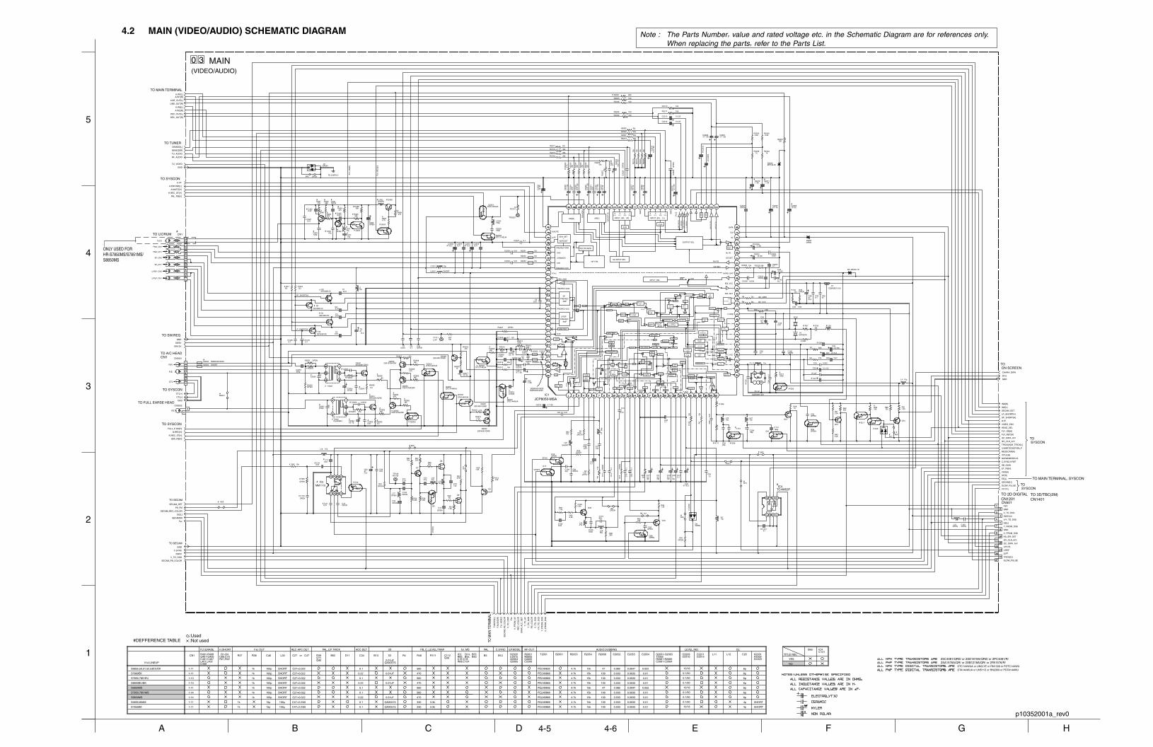
4-5 4-6
MAIN (VIDEO/AUDIO) SCHEMATIC DIAGRAM
HGFEDCBA
4
5
3
2
1
4.2
V14 LINEUP
S7850,7851EU
S6850MS
S7850,7851MS
S5800,80AM
S7855EE
1-11
QAX05752SC4081/QRS/ or 2SD1819A/QRS/ or 2PC4081/R/
DTA144WUA or UN511E or RN2309 or PDTA144WU
2SA1576A/QR/ or 2SB1218A/QR/ or 2PA1576/R/DTC144WUA or UN521E or RN1309 or PDTC144WU
#DEFFERENCE TABLE
S6855,50,51,52,53EU/EK
S8850MS
R68,C124
S7860EK
S8850EU/EK
R2001
AUDIO.DUBBING
T2051
PELN0860
PELN0832
PELN0832
CN1
1-11
1-11
1-13
1-13
330
R2002R401-R408Q401-Q405C401-C407L401,L402
FLY.ERASE
R4X2Q1-Q4
0.1
C69,C70R21,R22
Fsc OUT
R37 B52 R46D11 B3
1-11 3300.1
PELN0860 4.7k
0.01uF
R38 B55
560
470
560
470
15k
B13
ACC DET
C34
0.1
0.01uF
1-11
100
1-14
1-14
0.01uF
0.1
0.22
IC2, Q14,
0.033 0.0033
560
0.01
560
4700.01uF
R65,
0.1
0.22
R39Q11
for_MS
0.1
0.22
C112C2205C2206
RF-OUT
PELN0860
PELN0860
0.1/50
PELN0860
PELN0860
PELN0860
QAX0575
B2051 R2054 R2056
4.7k
4.7k
4.7k
4.7k
4.7k
4.7k 15k
4.7k
4.7k
QAX0575
R2053
12k
12k
15k
15k
15k
100 0.033
15k
15k
R111
47
47
100
100
100
0.0033 0.01
100
100
3.3k
C2052 C2053 C2054
0.082
0.082
0.033
0.033
0.033
Q40
L11
0.033
0.033
3.3k
0.0047
0.0047
0.0033
0.0033
0.0033
10/16
Q39
0.0033
0.0033
REC APC DET
0.022
0.022
0.01
0.01
0.01
C27 or
0.01
0.01
C47 Q2061-Q2063 L12T2052R2061-R2065C2061-C2064
LEVEL.IND.
C25 K2001K2002K2003
C2209C2210
C2211C2212
C27=0.022
CE
6p
6p
6p
6p
6p
6p
6p
4p
4p
SHORT
C46
SHORT
L30
1k
1k
10/16
10/16
0.1/50
0.1/50
0.1/50
1k
1k
0.1/50
0.1/50
1k
C27=0.022
C27=0.022
1k
1k
1k
1k
100p
100p
100p
100p
100p
EP.MODE
100p
100p
15p
15p
SHORT
SHORT
SHORT
B12Q2004
C.SYNC
SHORT
PALPB_C_LEVEL/TRAP3D
TITLE REC
PAL_EP TRICK
SHORT
H.SHORT
YES
NO
B65
B25, B50C76-C78
IC4C141
SHORT
SHORT
100µ
100µ
C2015
C27=0.022
C27=0.022
C27=0.022
C27=0.022
C47=2.2/50
C47=2.2/50
Q2005
R2020
C409
:Used:Not used
IC1
C114
C12
C84
R117
R3
C139
R35
Q17
C22
L20
L2
TU_VIDEO
C11
C14
C15
Q40
C13
C16
C80
C24
Q11
C32
Q2251
C65
C17
CN1
C19
D8
B9
C28
L11
L4
F.A
UD
IO[R
]
Q25
Q26
C56
R118
C31
R9
R8
C40
C34
X1
X2C36
Q2055
L3
C21C20
R6
R36
R7
R39
Q18
C37
C39
R92
Q41
Q24
CN501
C109
Q21
GND
IC2
L15
C77
C60VHS[H]
Q7
Q8
C70
C1
Q4
Q2
R21 R22
C6
C69
C5
L1
Q1
Q3
R93
C2
C3
R111
C4
C2013K2002
K2001
C47
C7 C44C8
C61
Q5
R23
R91
GND
SW5V
SW12V
Q9
V.P.CTL
R24
C_F
RO
M_D
IGI
Y_F
RO
M_D
IGI
R48
C_T
O_D
IGI
Y/V
_TO
_DIG
I
C71
R25
R26 R28
R27
Q6
C72 L18
R29
L19
C74
C73
R31
R32
R30
C78
C75C76
R37
L13
F.A
UD
IO[L
]
C33
Q14
C64
DEC_OUT[R]
DEC_OUT[L]
LINE_OUT[R]
R54
A.IN2[R]
R46
A.IN2[L]
LINE_OUT[L]
L30C46
L27
C108
A.IN1[R]
R70
A.IN1[L]
SLOW_PULSEB13
C63
R38
R4
R104
R5
Q38
L24
R41
R68
C106
C23
R65
C124
TRICK[H]/M_TRICK[L]
R22
27
R40
R42
D11
K2003
EE[L]
K2004
Q2006
C45
Q10
SECAM[H]
C25
C35
R2023
C26
GND
L28
C38
Y_T
O_S
UB
R51
Fsc
SECAM_DET
SECAM_REC_COLOR
SW5V
C401
C402
C403
C405
C404
C406
C407
C9
R401 R402
R404R406
R408
R407
R403 R405
L401
Q401
Q402
C59
Q405
Q403
Q404
C110
SECAM_DET
V.PULSE
EE[L]
SB_GAIN
R90
SP[H]
C.SYNC
R2022
C.SYNC/V.REF
TU
_VID
EO
3.58NTSC[H]/P.ON_P
I2C_CLK_A/V
I2C_DATA_A/V
C2017
D.FF
NORM/MESEC/S
HEAD_SEL
FLY_REC[H]
V_TO_OSD
SP_SHORT[H]
LP_SHORT[H]
C409
SECAM_PB_COLOR
PB_FM
B52
C140
B55
Q39
IC4
V_T
O_O
SD
V_F
RO
M_A
V
Fsc
SE
CA
M_P
B_C
OLO
R
C141P
B_C
OLO
R
Y_T
O_A
V
RE
C_C
OLO
R
2Fsc
B65
CHARA_DATA
L402
R1C112
C2231
C10
R2
C142
Q16
L31
C2204
C143
SECAM[H]
MA
IN_A
LC_D
ET
GND
R62
Q28
C82
ET_PB[H]
B8
B3
K2251
C2016
R2211
TP106
TP111
C29
C27
R2226
TU_AUDIO
L2252
C2255
Q2252
R2210
C2254
R2013
R2014
C2006
R2015
C2007
C2008
C2010
C2009
R2016
C2011
R2017
Q2003
R2018
R2019
Q2002
Q2001
R2208
C2253
C2214
C2213
C2012
SEP_PB[H]
C2003 C2251 C2252C2004
L2251
L2001
R2203
C2227
TP2253
C22
26
C22
25
C22
23
C22
22
C22
20
C22
19
R2220
R2219
R2218
R2217
R2213
R2007
R2006
R2005
C22
17
C20
02
R2209
C22
10
C22
15
C2208 C2001
R20
09
R20
08
R22
22
R22
23
R22
24
R22
25 R20
10
R22
15
R2205
R2202
R2204
IND[L]
IND[R]
C2212 C2211
PAL_PB[H]
R2021
H.REC_ST[H]
N.REC_ST[H]
FLY_ON[H]
C22
09
DEMOD[R]
A.FF
A.MUTE[H]
C30
DEMOD[L]
C22
18
C22
16
RF_AUDIO
A.ENV/ND[L]
R2206
R2003
C2015
Q2004
C2205
C2203
R2055
C2201
C2202
VIDEO_ENV
C2207 C2206
R2001
R20
02
R2251
C22
21
C22
24
D2201
D2202
R2201
C2005
R2056
C2054C2055
C2053
R2054
Q2051
C2052
Q2053
C2051
N.REC[H]
Q2063
B42
D1
Q2052
C2014
CTL[-]
CTL[+]
GND
R2052 Q2054
R2051
R2053
T2051
R2060
R2059
R2058
R2057CN2001
Q2062
C2061
T2052
Q2061
R2062
R2061
C2062
C2063C2064
R2064
R2063
CN2002
B2051
FULL_E.ON[H]
R2065
C22
28
R2228 R2229
R2020
Q2005
C103
C93
L17
MESECAM[H]
R75
R77
L12
L5
R79
R113
K2253
K2252
C22
30
C22
29
D6
R88
B50
R33
B12
B25
180p
12p
100K
1.8k
47p
47
68µ
0.1
0.1
0.01
0.1
0.01
0.1
0.1
1
3.3 2.2
3.3
12µ
10µ
47
0Ω
0Ω
10
4.7
10µ
0.11
27k
1.8K
680
10k
1
0.1
1.5k
0.22
10µ
0.01
47
0.1
0.01
0Ω 0Ω
0.01
0.1
47
10µ
2.2k
0.01
0.01
0.01
68p
0.001 0.1
0.01
1.8k
1k
0.01
10k
6.8k 220
220
47p 22µ
560
12µ12p
1.5k
470
0Ω
0.01
0.01
33µ
2.2
22p
1.5k
33µ
68p
0Ω
0.1
0Ω
6.8k
0Ω
27µ
3.9k
820p
0.1
10k
12k
2.2k
680
0.1
0.01
47k
0.1
68µ
47
1.2k
0.01
0.22
130p47p
0.001
15p
2.2
220 680
47k39k
47k
4.7k
560 68k
15µ
0.01
82p
390
1k
10
0.1
6.2k
150p
1.5k
0.001
0.1
100
0Ω
33p
10k
0.033
12k
150µ
180p
10k
0.01
6.8k
220k
0.012180
224.7
0.0015
0.001
39k
4.7
18k
4.7k
4.7k
100
0.01
10
10
4.7
47 47 0.010.01
10µ
2.2k
0.1
10 4.7
0.47
0.47
4.7
10
39k
39k
39k
0Ω
39k
39k
39k
0Ω
10 10
100
4.7
4.7 4.7
12k
12k
12k
12k
12k
15k
12k
15k
1k
2.2k
1k
1 1
0.47
0.47
0.47
100
100
0.0068
1
10
3.3
0.1
0.033
47 10
680
2.7k
1k
0.01
0.01
120
4.7
82
10
330p
18k
47k
18k
47k
0.033
3.3
27k
0.0033
0.0110
47K
150
18k
0.1
10k 56k
390
10k
100
0Ω
0Ω
0Ω
15k
JCP8050-MSA
OPEN
OPEN
/6.3
SHORT
OP
EN
DTA144WUA
/50
/50 /50
OPEN
OPEN
/50
OPEN
OPEN
/6.3
/25
QAX0576
/50
DTC144WUA
/50
/50
FSC
GND
C_TO_DIGI
SW5V(2)
V/Y_TO_DIGI
EE[L]
Y_FROM_DIGI
GND
C_FROM_DIGI
KILLER_DET
I2C_CLK_A/V
I2C_DATA_A/V
V.P.CTL
V.REF
D.FF
TRICK[H]
SLOW_PULSE
MM1113
/6.3
2SC4081/S/
2SC4081/S/
/6.3
2SC4081/S/
2SC4081/S/
NQR0403-003XNQR0403-003X
OPEN
OPEN
OPEN
OPEN
OPEN
/50
OPEN
OPEN
NQR0403-003X
SHORT
2SC4081/QRS/
/6.3
OPEN
/50
/25
OPEN
OPEN
TC4W53F
SHORT
±40.5%
OPEN
±2%
±0.5%
OPEN
OPEN
OPEN
OPEN
OPEN
0
DTC114EUA
/16
/50
/50
DTA144WUA
2SC4081/QRS/
2SC4081/QRS/
/25
/25
/50
/6.3 /6.3
SHORT
/25
/50 /50
/50
/50
/25
/25
/25 /50
/50 /50
/50 /50
OPEN
/50
/50
DTC144WUA
/50
/25
/16 /25
OPEN
MTZJ8.2C
/50
/25
2SC4081/QRS/
MY
DTC144WUA
OPEN
DA204
2SA1576A/QR/
OPEN
OPEN
P/R
A.E
CTL
2SA1576A/QR/
OPEN
2SA1576A/QR/
MY
PELN0861
2SC4081/QRS/
/16
FE
DTC114EUA
OPEN
OPEN
OPEN
OP
EN
QQR0967-001
QQR0657-019
OPEN
OP
EN
OP
EN
MTZJ5.1C
#
#
#
#
#
#
#
#
#
#
#
#
#
#
# #
#
#
#
#
#
#
#
#
#
#
#
#
##
#
#
#
#
#
#
#
#
#
#
#
#
#
#
#
#
# #
#
# #
#
##
#
#
#
#
#
#
#
#
#
#
#
#
#
#
#
#
#
#
# #
#
#
#
#
#
#
#
#
#
#
##
#
#
#
#
#
#
#
#
#
#
##
#
#
#
#
#
#
#
#
#
#
TO MAIN TERMINAL
TO ON SCREEN
0 3 MAIN(VIDEO/AUDIO)
DETD.FF
PRE/REC GND
PB FM
TO M
AIN
TERM
INAL
H
H
TO SYSCON
PRE/REC VCC
L H
D.FF
SPPRE/REC
AMP
LP/EPPRE/REC
AMP
ENV OUT
TO SHEELD
SP1
SP2
COMMON
COMMON
LP/EP1
C.S
YN
C
LP/EP2
A.Vcc
VH
S[H
]
VHS[H]
SP[H]
SP_SHORT[H]
LP_SHORT[H]
FLY
_RE
C[H
]
FLY
_ON
[H]
A.FF
EVR
ENV DET+
PRE/REC GND
PRE/REC VCC
CH1
CH2
COMMON
-10dB
-10dB -10dB
-10dB
AGC
I2C_CLK
I2C_DATA
ALC
FBC
AGC DET
PB ALC
SYNC SEP
6dB
6dB
SQUELCH
D1*
D24
FLY.E
FMA_CH1
FMA_CH2
SP_CH1
SP_CH2
LP/EP_CH1
LP/EP_CH2
Y-LPF
P.C.
CLAMP
CLAMPCLAMP
Y VCC
CLEAR
N.C.D.E.
YNR
LPF
OFFSET
Y GND
N.L.
ET
Y
FBCALC
MAIN
DE EMPH.
REC
W.C./D.C
MAIN
VCA
CARREA
S-DET
CARR./DEV.ADJ
MOD
LPF
SUB LPF DE MOD D.LIM.
DO DET
G EQ
P EQ
SQPB DL
FM AGC
DET
MUTE
629TRAP
COMP
BDL GND
SB GAIN
C-SQUELCH
KILLERDET OUT
1/22FL VCO
REC APC
PB APC
REC AFC
ACC DET
X'talVCO/XO
CR DET2Fsc OUT
LPF2FscVCO
Fh LOCK CTL
C VCCPULSEGEN.
DISCRI
APC SW
C.KILLERID DET
DOWN CONV.
4PHASE GEN.
1/2PHASE SW.
TANK
MESECAM
IIC LOGIC
CLK
DATA
WHITE
BDL DET
CNV.NT on PAL
BDL VCC
CVCA
CCD LPF
SQPB
LEVEL DET1 LEVEL DET2
REC LEV.
TRAPLPF
C.K.ACC
2M LPF
HPF
BPFPILOT BURST
CTL.P.TRAP
EMPH./DE EMPH.
C-LPF
MAIN MAIN
CONV.1 CONV.2
C-LPF
DL
Fh TRAP
EQ
LPF
BDL
EMPHA.
SYNC
DET
CTL
C GND
BDL
42P
IN[L
]
42P
IN[L
]
D17CTL
INT
EXT
R
R
R
R
R
R
R
R
R
R
R
R R
R
P
P P
P
P
P
P
P
P
P
P
P
P
DO DO&REC
ET
ETSQPB
SQPB
SQPB SQPB
SP
SP
SECAM
SECAM
D1*D18
D1*D18
SECAM SECAM
SEP
COMP
P
D5 D5
CH1
CH2CH3
CH4
ADD
C.K.
LIM.
D1*
D24
D4
D4
NA INPUT SELHIFI FM
FM
MO
N
REC/PB MON
NR[L]NR[R] INPUT_SEL INPUT_SEL [L][R]
DET
LIN
E O
UT
[L]
LIN
E O
UT
[R]
fsc IN
CR DET
NA PB
NA REC
BAND_GAP
CLK
DATA
9V
Vcc
/2GN
D
NA
EX
T IN
LOG
OUTPUT SELNOR DET
LOGG
ND
1
A.MUTE
EVR
HIFIINPUT_SEL
HIFI
DC PB
A.GND
(TU)(TU) (FR)(FR) (L1)(L1)(L2) (L2)
DE
C O
UT
[R]
DE
C O
UT
[L]
BS
IN[L
]
BS
IN[R
]
22 33 44 1
5 5
0Ω
TO TUNER
TO SYSCON
TO U.DRUM
ONLY USED FORHR-S7850MS/S7851MS/S8850MS
TO SW.REG
TO SYSCON
TO SYSCON
TO A/C HEADCN1
TO FULL EARSE HEAD
TO SECAM
TO SECAM
TO 2D DIGITALCN1201
The Parts Number, value and rated voltage etc. in the Schematic Diagram are for references only.When replacing the parts, refer to the Parts List.
Note :
p10352001a_rev0
TO SYSCON
TO MAIN TERMINAL, SYSCON
TO 3D/TBC(2M)CN1401
Ω

4-7 4-8
1
2
3
5
4
A B C D E F G H
MAIN (ON SCREEN) SCHEMATIC DIAGRAM4.3
EE
OTHER
IC201
LC74775-9750
LC74776-9791
R209
5.1k
6.8k
# DIFFERENCE TABLE
2Fsc
V_TO_OSD
V_FROM_OSD
GND
SW5V
C222
D201
B214
C209
C225
R201
C218
R226
CHARA_DATA
R208
CHARA_DATA
L204L201
R213
R224
Q208
R225
GND
R220
C216R211
RF_VIDEO
R212
B206
L203
D202
D203
Q207
B203
B204
C204L202
IC201
C201 C202
R216
C217
L206
C214 C215
R210
C213C212
R209
C211C210C208C207C206
P.MUTE[L]
SYNC_DET[H]
I2C_CLK2
I2C_DATA2
OSD_CS
S.CLK
S.DATA_FRSYS
R20
4
R20
3
R20
2
1
1.5k
0.47
220
0Ω
1
1k 2.2k
10µ1µ
0Ω
100
470
5.6K
100
22µ
100
100
0.01
220
10K
56p
22µ
0.22 0.22
1.8k
4.70.1
100p100p33p33p
10k
/10
/50
2SC4081/QRS/
OPEN
OPEN
OPEN
2SA1576A/QR/
SHORT
SHORT
SHORT
VS
S1
XTA
L_IN
MU
TE
CH
AB
LK
LN21
OS
C_I
N
OS
C_O
UT
SY
NC
_DE
T
CS
SC
LK
SD
ATA
VD
D2
CR
_OU
T
VC
O_I
N1
VS
S3
VD
D3
VC
O_RNC
CV
OU
T
VS
S2
CV
_IN
CV
CR
VD
D1
SY
NC
_IN
SE
P_C
SE
P_O
UT
I2C
_DAT
A
CD
LR
RS
T
VD
D1
/6.3 OPEN
/25
OPEN
OP
EN
OP
EN
#
#
VIDEO/AUDIO
0 3 MAIN
TO SYSCON
TO SW.REG
TO TUNER
TO MAIN TERMINAL
(ON SCREEN)
The Parts Number, value and rated voltage etc. in the Schematic Diagram are for references only.When replacing the parts, refer to the Parts List.
Note :
SHORT
TO
p30088001a_rev0

4-9 4-10
MAIN (SECAM) SCHEMATIC DIAGRAM
HGFEDCBA
4
5
3
2
1
4.4
The Parts Number, value and rated voltage etc. in the Schematic Diagram are for references only.When replacing the parts, refer to the Parts List.
Note :
p30087001a_rev1
# MARKS ARE NOT MOUNTED ON EE MODELS
C322
C315
R318
L304
SECAM_PB_COLOR
SECAM_DET
SECAM_REC_COLOR
V_TO_OSD
SW5V
C.SYNC
GND
Fsc
SECAM[H]
R328
R329
C313
R326
R327
C30
2
C306
C319
EE[L]
PB_FM
C324
Q303
R317B302L301
C323Q301
R314
R302
C30
3
C30
4
C309
C305
C310
C311
L302
R303
C307
R305
R308R307
R306
B301
Q311
Q312
R301
R321C301
Q302
C312
C318C320 C316
L303 R311
C314R310
R313
C317
R312
R315
R309
R304
R316
C308
C321
IC301
0.47
1
820
100µ
0
0.47
1
1
1
39p
10µ
47
24k
120k
0.00
68
0.00
68
0.1
0.01
0.01
0.01
6.8µ
27k
150p
47k
2.2k2.2k
27k
27k
150p
0.001
0.0220.01 0.01
27µ 4.7k
22k
22k
680p
2.7k
560k
0Ω
6.8k
120k
0.01
300p
OPEN
OPEN
OPEN
OPEN
OPENSHORT
/6.32SA1576A/QR/2SB1218A/QR/
2PA1576/R/
±0.5%
OPEN
OPEN
OPEN
OPEN
DTA144WUAUN511ERN2309PDTA144WU
OPEN
±2%
LA7358
#
#
#
#
#
#
#
#
#
# ##
#
#
#
FILT.
0 3 MAIN
TO VIDEO/AUDIO
(SECAM)
SYNC GAIEGEN./V-SEP
B BGPGEN
AFC
4.43MHZVCO
SECAMDET
4.3MHZOSC
F0ADJ.
ADJ.F0
PHASE
LOGIC
DET
FROM LIM
OSC1.1MHZ
CA
VA
IREF
MODECTL
X2 2.2MBPF X2 4.3M
BPF
VCC
GND
PBMUTE
4.2VREG
R/P
AGCAMP DET
AGC
PBMUTE
IREF
LIM
4.3MHZBPF
B
1.1MBPF
SYNCGATE 1/4
SYNCGATE
TO MUTE
TOREC MUTE
FILT.
LIMITER
R P
RP
R
P
R
PR
PVA
CA
TO P
HASE
DET
PB MUTE
TO
B
ADJ
HOLD
DET SENSECONTROL
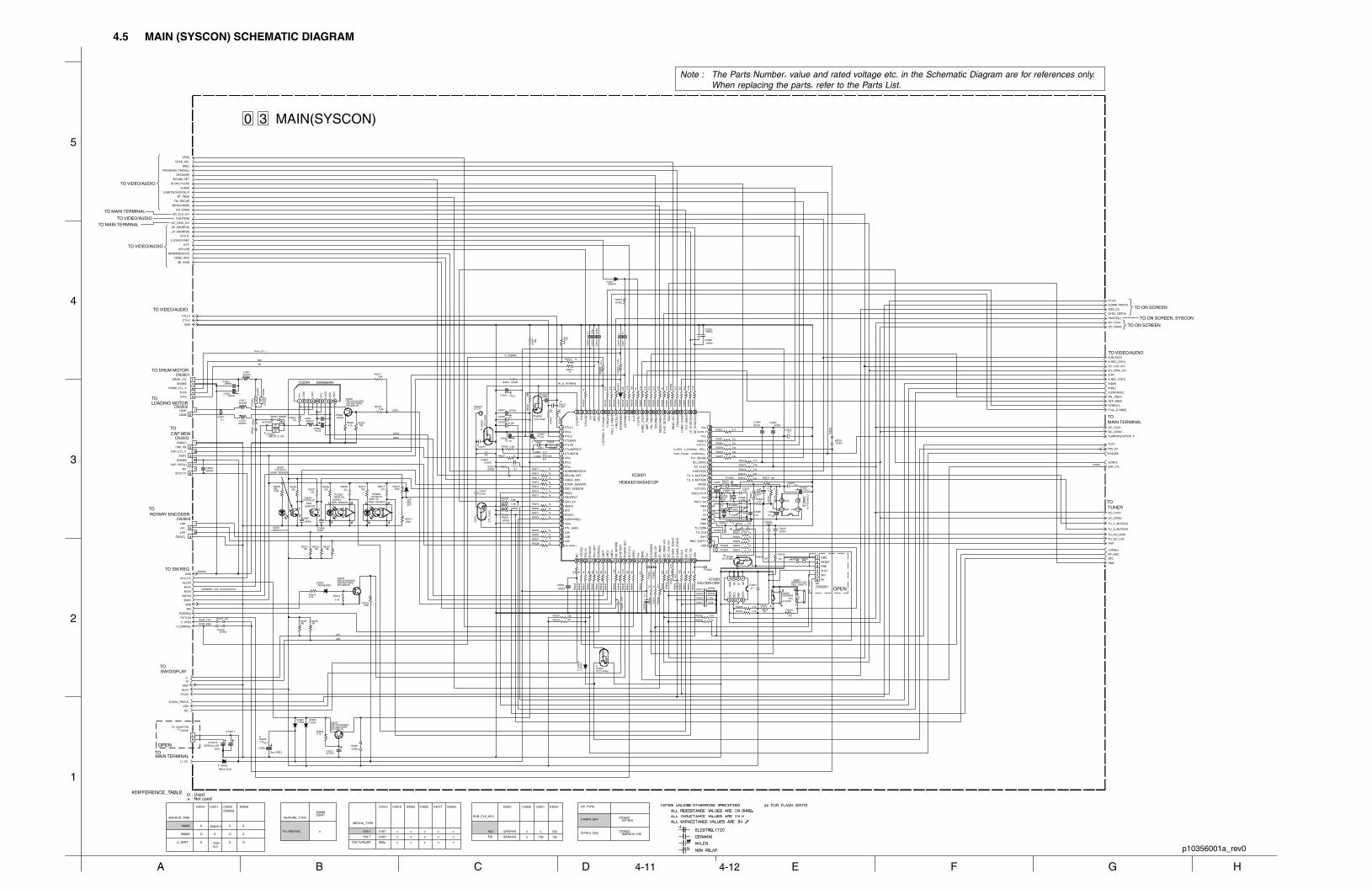
4-11 4-12
1
2
3
5
4
A B C D E F G H
MAIN (SYSCON) SCHEMATIC DIAGRAM4.5
o
Y29-T+PALEP
O
BACKUP_TIME
10MIN
60MIN
LI_BATT
D3006C3010 C3011 C3042CN3006
X
X
X
X O
XO
FEATURE_TYPE
TV-LINK(P50)
D3008Q3007
MECHA_TYPE
Y29-2
Y29-T
C4015 C4016 Q4002 C4005 C4017 Q4003 ##_FOR_FLASH_WRITE
#DIFFERENCE_TABLE
SUB_CLK_ADJ
ADJ
FIX
X3001
QAX0444
QAX0445
C3025 C3041 C3024
22p
12p10p
o x
x
x
x
x xx
x
x
o
o
o
o
o
o
o
x
0.001
0.001
680p1000/6.3
3300/6.3 X X
CP_TYPE
Leaded_type
Surface_type
ICP-N25
NMFZ012-1R0
CP3002
CP3003
IC3001
R40
03
C3017
C4001
X3001
R3083
R32
29
C4007
V_DOWN[L]
R4005
C40
12
C4003
C3032
C30
16
TP
3901
R3012
R3013
R3014
R3015
R3016
R3017R3018
B3079
R3020
TP
3902
Q3007
C3018
R3217
R3025
R3026
R3027
R4008
R3081
R3076
R3021
R30
30
R30
31
TP3903
TP3905
TP3904
R3073
R3072 R3071
C3025
C30
33
FLY_ON[H]
3.58NTSC[H]/P.ON_P
R3066
R3022C3024
C3030
R3062
R3061
R3060
R3080
R3058
R3057
R40
04
R3224
R40
13
R3069
R4017
R4018
D3006
R31
05
R3075
S.CLK
C3049
R40
12
R40
11
R40
10
R40
09
R30
97
R30
96
R30
95
R30
94
C3034
R30
92
R30
91
GND
R30
89
R30
88
R30
87
R30
86
R30
85
C3022
R32
31
R32
30
C3026
R30
29
R30
35
R30
36
C3020
R30
42
R30
46
R30
47
R30
48
R30
32
R30
38
R30
39
R30
40
R30
41
C3021
C4004
R30
44
S3001
C3035
C3028
C3029
R30
49
R30
50 R30
51
R30
52
R30
53
R30
54
R30
55
R30
56
C3031C3050
R3201
R3204
R3202
Q3001
R3203
IC3004
C3002
C3003
C3001
CN3002
Q3002
Q3003
L3001
R3206R3207
X30
02
C3037R3205
D3001
R3213
R3212
D30
02
PC3001 PC3002
R3208 R3210
CN3004
R3214
R3211R3209
C3036
D30
08
C3004
C4008
R3233
CN3003
CP
4001
R40
20
IC3003
R3223
S3002
C3027
D3004 D3005Q3005
M12V
C4002
R3222
C3012
C4006
R30
33
R3074
C4015
B3179
R3241
B3070
C3010
C3011
B4001
IC30
02
P.CTL[H]
R31
06
R31
04
M12V
SW12V
SB_GAIN
CP3002
GND
SW5V
GND
AL5.8V
48V
S.DATA_FRSYS
CN3006
B30
05
B3004
C3014
R3225
M12/17V
R4007
R40
19
MESECAM[H]
R30
93
SP_SHORT[H]
R.PAUSE
LP_SHORT[H]
CTL[+]
VIDEO_ENV
R3011
C.SYNC/V.REF
SECAM_DET
C3039
C3038
R3234
P.MUTE[L]
N.REC_ST[H]
R30
34
SYNC_DET[H]
P50_I/O
IND[R]
IND[L]
R30
90
C30
54
P.SAVE[L]
D.FF
R3235
STB
R3236
A.MUTE[H]
J1
R3019
V.PULSE
CTL[-]
B3279
B39
71
EE[L]
A.FF
C40
14
C40
13
C40
11
B3966
C4009
D40
02R
4015
R4001
C4016
D4001
R4016
C4005
TP4001
Q40
01
C4010
A.ENV/ND[L]
RF_AGC
AFC
LOCK[L]
S.DATA_FRSYS
OSD_CS
S.CLK
I2C_DATA_A/V
I2C_CLK_A/V
Q40
03
L3011
B3962
NORM/MESEC/S
SAT_CTL
A.MUTE[H]
SEP_PB[H]
I2C_CLK_A/V
H.REC_ST[H]
I2C_DATA_A/V
R31
03
J2
I2C_CLK2
I2C_DATA2
RC
I2C_CLK2
I2C_DATA2
AL5V
CN3901
TU_A_MUTE[H]
TU_V_MUTE[H]
GND
V.P.CTL
Q3901
SCR[H]
R4006
C4031
R3215 R3216
Q4002
TU_I2C_CLK
TU_I2C_DATA
R3219R3218
D3003
Q3004
R3220
C4032
I2C_CLK2
I2C_DATA2
C3015
CP
4002
CP3003
L4001
R3059SW1
R3077
SW2
R3078
R3079
3.58NTSC[H]/P.ON_P
FLY_REC[H]
FULL_E.ON[H]
VHS[H]
ET_PB[H]
SLOW_PULSE
SECAM[H]
PAL_PB[H]
TRICK[H]/M_TRICK[L]
SP[H]
HEAD_SEL
TP3906
TP3908
N.REC[H]
TP3907
LI_5V
C30
40R3237 R3238V_UP[H]
AL5V
L3012
R3063
R3242
CN3001
R40
21
C3041
R3247
R3246
R3252
C3007
C3008
C3042
C4017
R3239R3240
560
0
1M
0.0015.6k
1
0.001
0.1
0.1
1k
1k
1k
1k
1k
1k
6.8k
1k
5.6k
1k
1k1k
1k
0
470
1k
1k 1k
0
0 10k
30p
0.1
4.7k
1k
47
10k
1k
1k
0
1k
1k
560
4.7k
1k
100
1k
1k
0
470
2.2k 4.7k
10k
1k 0 0 0 0 1k 0 0 0 0 2.2k
2.2k
0.1
1k
4.7k
0.01
1k 0 0
100p
0
1k 1k 0
1k 1.5k
1k 4.7k
0
100p
22
0 0 0
470
470
470
1k 1k 1k
0.1
0.1
10k
2.2k
4.7k 10k
10
0.1
18k18k 12p
180
330k
470k180 180
10k
27k27k
18p
1
10k
10K
4.7k
10
0.1
4.7k
47
47
0
0
0.001
10k
0
0
47
10k
1k
10k
0
1k
10k
0
3.3k
3.3k
1k
100p
0.05
6
0.1
0.056
5.6K
680p
0.0022
0.022
0
10k 10k
4.7k4.7k
100k
0.1
0
0
0
0
0.01
10k 10k
0
4.7K
10K
0.001
470
10k 10k
CTL[+]
SVss
CTL[-]
CTLBIAS
CTLFB
CTLAMPOUT
CTLSMTIN
CFG
SVcc
AVcc
AVss
Vss
Vcc
I2C
_DAT
A_A
/V
I2C
_CLK
_A/V
FWE
NMI
X2
X1
RES
OSC1
OSC2
Vss
VCC/VCL
MODE
Vcc
Vss
C.S
YN
C
A.F
F
V.F
F
CA
PP
WM
DR
UM
PW
M
DP
G
DF
G
Vcc
V.P
ULS
E
Vss
CT
LRE
F
CTL_GAIN
VIDEO_ENV
AFC
RFAGC
END_SENSOR
IND[L]
S.C
AS
S[H
]
START_SENSOR
A.ENV/ND[L]
IND[R]
NORM/MESEC/S
LSA
LSB
LSC
CAP_REV[L]
LMC
1
LMC
2
LMC
3
PROTECT
JSA
V.P.CTL
JSB
SY
NC
_DE
T[H
]
OS
D_C
S
RC
S.D
ATA
_FR
SY
S
S.C
LK
RM
O
SLOW_PH.R
EC
_ST
[H]
PO
WE
R_D
ET
SB
_G[P
WM
]
ST
B/T
ES
T
A.MUTE[H]
TU
_FG
SP
_FG
REC_SAFTY
TU_DATA
TU_CLK
I2C_DATA2
I2C_CLK2
SP
_SH
OR
T[H
]
P50
_IN
LP_S
HO
RT
[H]
TR
ICK
[H]
HE
AD
_SE
L
P50
_OU
T
SECAM_DET
SCR_ID/
LOC
K[L
]
P.S
AV
E[L
]
TU_A_MUTE[H]
TU_V_MUTE[H]
FLY
_ON
[H]
N.R
EC
_ST
[H]
HI_
FF
/RE
W[L
]
ME
SE
CA
M[H
]
SE
CA
M[H
]
R.P
AU
SE
SW1
SW
2
P.C
TL[
H]
ET
_PB
[H]
SP
[H]
FLY_REC[H]
3.58NTSC[L]
EE[L]
SE
P_P
B[H
]
PAL_
PB
[H]
P.M
UT
E[L
]
N.R
EC
[H]
FU
LL_E
_ON
[H]
V.UP[H]
VHS[H]
S.D
ATA
_TO
SY
S
P.ON_PULSE
V_DOWN[L]
V_D
OW
N[L
]
HD6432194SAD12F
OPEN
OPEN
FOR_E06
EE
[L]
OPEN
DTC144WU
OPEN
/6.3
RB721Q-40
OPEN
OPEN
/10
REC_SAFETYQSW0602-003
OPEN
OPEN
OPEN
2SD1819A/QRS/2SC4081/QRS/2PC4081/R/
VC
C
GN
D
Vre
f
LMC
1
LMC
2
LDM
1
LDM
2
BA6956AN
OPEN
/25
LDM2
LDM1
PTZ-NV16
PTZ-NV16
SHORT
1/4W
LNB2301L01VI
1SS
133GP3S123 GP3S123
LSB
LSC
LSA
GND[C]
1SS
355
OPENNC
CAP_FG
GND[C]
CAP_CTL_V
SW5V
GND[M]
CAP_REV[L]
M12/17V
CP
SH
OR
T
SD
A
SC
L
WP
VC
CA
0
A1
A2
VS
S
S.CASS
QSW0695 -001
/25
11ES2 11ES22SD1819A/QRS/2SC4081/QRS/2PC4081/R/
/6.3
/6.3
OPEN
EDLQEZ0244-229
OPEN
RST
VCC
VSS IC-P
ST
3427
U
V_DOWN
CPICP-N25
OP
EN
/6.3
OPEN
OPEN
OP
EN
OP
EN
OPEN
SH
OR
TOPEN
SHORT
OPEN
CTL.P
DT
C11
4EU
DT
C14
4W
SHORT
GND
RESET
FWE
AL5V
SIO
SII
DTC144W
OPEN
OPEN
HI_S_FF/REW
DTC144W
RD39ES/B3
2SD1819A/QRS/2SC4081/QRS/2PC4081/R/
OPEN
OP
EN
CP
CP
NMFZ012-1R0
SHORT
FOR_17V
SHORT
GND[M]
DRUM_CTL_V
D.PG
D.FG
DRUM_12V
OPEN
OPEN
OPEN
OPEN
/6.3
[for_EDL]
OPEN
#
#
#
#
#
#
#
#
#
#
#
#
##
##
#
#
##
##
##
#
#
#
#
#
REEL SENSOR REEL SENSOR
LMC3
SUPPLY TAKE UP
START SENSOR
SENSOREND
GND[M]
TOSW/DISPLAY
TO SW.REG
TO TUNER
TO_SHORT-PIN
TO
[IN]
TO DRUM MOTOR
LOADING MOTORTO
CAP MDA
TO ROTARY ENCODER
[OUT]
0 3
dfg
dpg
drum_ctl_v
MAIN(SYSCON)
MAIN TERMINAL
JSA
JSB
TO
[RMO]
LMC1
LMC2
COMMON_USE_M12/DRUM12V
ΩΩ
Ω
ΩΩΩΩΩΩΩ
Ω Ω Ω Ω Ω Ω Ω Ω Ω Ω Ω Ω
Ω
Ω
Ω
Ω
Ω
Ω
Ω
Ω
Ω
Ω
OPEN
The Parts Number, value and rated voltage etc. in the Schematic Diagram are for references only.When replacing the parts, refer to the Parts List.
Note :
p10356001a_rev0
TO VIDEO/AUDIO
TO VIDEO/AUDIO
TO MAIN TERMINAL
TO VIDEO/AUDIO
SHORT
0Ω
24LC32A-I/SW
OP
EN
OPEN
TO ON SCREEN
TO VIDEO/AUDIO
TOMAIN TERMINAL
: Not used: Used
TO MAIN TERMINAL TO VIDEO/AUDIO
TO ON SCREEN
TO ON SCREEN, SYSCON
OPEN
OPEN
OPEN

4-13 4-14
MAIN (SW.REG) SCHEMATIC DIAGRAM
HGFEDCBA
4
5
3
2
1
4.6
#DIFFERENCE TABLE
HIGH SPEEDFF/REW
-YES-
-NO-
Q5301Q5311D5209
C5208K5301
##MARK ELEMENTS ARE NOT MOUNTED
R5324
R5325
D5307
11ES2ERA15-021A3G
SHORT
POWERSAVE
-YES-
-NO-
B5301 D5302R5101R5102 R5104
Q5308R5320R5321 B5303
Q5312Q5318Q5320
D5317
R5317R5327R5329
R5330
330k
220k
150k2W
2W68k YES
1S133
#DIFFERENCE TABLE
YES
YES
YESNO
SHORT NO
NO
NO
#DIFFERENCE TABLE
CE
OTHER
B5001B5002 C5002 LF5001
#DIFFERENCE TABLE
LF5002
QQR0978-001QQR0608-001QQR0609-001QQR0610-001
QQR0532-001QQR0533-001QQR0516-001QQR0932-001QQR0816-001
YES
YES YES
NONO
NO
EP
-YES-
-NO-
Q5323Q5322
R5344R5345
D5318D5319
SHORT
11ES2ERA15-021A3G
YES
NO
LEVELIND.
-YES-
-NO-
D5201
AK0411EQS041S4
AU01Z10ELS2
R5326
2.2
SHORT
YES
NO
#DIFFERENCE TABLE3 4 5
1SS270A
T5001
QQS0033-001QQS0034-001
QQS0030-002QQS0031-002QQS0036-001
#DIFFERENCE TABLE 6
SURGE
PHILIPS110-240V
OTHER
VA5003
YES
NO
D5305
AK0411EQS041S4
11ES2ERA15-021A3G
R5316
12k
10k
1 2
DC3.5V[-]
AL5.8V
Q5309
-28V
DC3.5V[+]
R5317
R5318
D5001
SW5V
SW12V
P.CTL[H]
Q5310
LF5001
D5210
P.SAVE[L]
GND
C5310
R5323
C5106
D5206
C5309
Q5312
BT2
L5301
C5001 C5002
Q5304
Q5318
D5310
C5301
C5207
Q5305
D5205
R5322
D5203
R5104
D5101
D5102
C5101
R5102
D5306
C5303
D5303
R5307
CP5301
D5202
PC5101
Q5320
LF5002
C5006
R5106
Q5101
R5107
C5104
R5103
D5103
R5101
CH+12V
K5101
T5001
R5311
C5103
IC5301
C5304
D5305
C5102
D5201
Q5307
D5211
C5205
C5203
C5202
C5201
C5311
C5204
D5301
R5304
D5309
C5206
L5202
L5201
C5004
R5302
R5319
C5307
D5304
C5308
D5316
F5001CN5001
RF5V
C5302
D5317
D5302
B5302
D5209
C5208Q5301
R5324 R5325
R5316
R5332
R5315
Q5311
Q5323
Q5302
R5314
K5102
VA5003
Q5303
R5306
M12V
M12/17V
V_UP[H]
CP5302
D5307
R5112D5105
C5107
R5110R5308
C5352
R5309
R5344
Q5102
C5003
R5305
R5310
D5204
C5306
C5305
R5345
R5312
48V
R5303
V_DOWN[L]
R5313
B5002
Q5319
B5304
R5328
B5001
K5301
D5318
D5308
R5301
C5105 R5109
R5111
D5208
R5108
D5319
CP5304
CP5303
Q5322
C5351
R5326
R5330
R5327
Q5306
B5303 R5329
R5320 R5321Q5308
B5301
47k
220
100
47k
270p
10
100µ
0.068 0.033
100
100
220
0.0047
100
68
0.39
330
1
68k
10k
0.001
33p
10
1200
680
220
0.01
4.7
470
47
33µ
33µ
0.0022
1k
220
47
100
T2AL
47
180
4.7k 2.2k
2.2k
1k
220
220
0.1
220k470 10k
4.7k
1k
220
0.22
560
3.3k
1.2k
3.3k
2.2k
4.7k
0.018 680
560
1.2k
1k
2.2k1k
27k 27k
2SD1450/ST/2SD1302/ST/
1/4W
FR
S1WB/A/60-4102S1WB/A/60S1WB(A)60F4072X
DTA114EUAUN5111RN2302PDTA114EU
PELN1204-01-01QQR0977-001
AU01Z1SR153-400ERA18-0210ELS2PG104RS
/16
/50
FMB-24FSQ05A04BYG801C04SF5SC4SB640FCT
/50
2SD2144S/UV/
/250
MY
/250
MY
2SC3616/ML/
DTA114EUAUN5211RN2302PDTA114EU
1SS1331SS270A
/16
/16
DTA114EUAUN5111RN2302PDTA114EU
AU01Z10ELS2
AU011SR153-400ERA18-0410ELS4
AU011SR153-400ERA18-0410ELS4
/1k
MTZJ11CRD11ES/B3/
/16
RD5.1JS/B2/MA4051N/M/
CP
ICP-N38
FML-12SFCF06A20YG901C2SF5LC20UER602FCT
PC123F2PS2561L1-1/WL/ON3171/R/
UN5211DTC114EUARN1302PDTC114EU
/400
1W
2SK26322SK2129
1/2W
/50
1SS1331SS270A
QQR0678-001QQR0621-001
L5431
/50
/1k
2SD2144S/UV/
AU01Z1SR153-400ERA18-0210ELS2PG104RS
/50
/10
/16
/6.3
/50
/100
MTZJ15CRD15ES/B3/
MTZJ27CRD27ES/B3/
/25
/250
/16
1SS1331SS270A
/16
SHORT
/250
/16
1SS1331SS270A
ERA18-021SR153-40010ELS2PG104RS
/25
2SB1256
DTC114TUAUN5215RN1311PDTC114TU
2SB927/ST/
2SD2375/QP/
SHORT
QAF0026-621
2SD1819A/RS/2SC4081/RS/2PC4081/R/
CP
ICP-N25
1SS1331SS270A
/50
MY
2SD2144S/UV/
AU01Z10ELS2
MY
/50
MY
1/2W
2SD1819A/RS/2SC4081/RS/2PC4081/R/
SHORT
MTZJ11BRD11ES/B2/
/50
MY
RK1421DQ04SB240
CP
NMFZ012-1R0
CPNMFZ012-1R5
DTC114TUAUN5215RN1311PDTC114TU
SHORT
UN5211DTC114EUARN1302PDTC114EU
2SA1576A/RS/
##
#
##
#
##
##
##
#
##
#
#
##
##
#
#
##
##
##
##
#
#
D
GS
#
#
##
#
#
##
##
##
##
#
#
#
##
# #
#
##
#
#
#
##
#
##
#
##
##
##
##
##
#
#
#
##
# #
#
#
#
##
# ##
#
BRNLIVE
NEUTRALBLU
30 MAIN(SW.REG)
The Parts Number, value and rated voltage etc. in the Schematic Diagram are for references only.When replacing the parts, refer to the Parts List.
Note :
GROUND POINT FORPRIMARY VOLTAGE
DANGEROUS VOLTAGE
GROUND POINT FORSECONDARY VOLTAGE
0Ω
0Ω
TO SW/DISPLAY
TO SW/DISPLAY
TO SYSCON
TO SYSCON
TO SYSCON
TO SYSCON
TO SYSCON
TO VIDEO/AUDIO, ON SCREEN,SYSCON, TUNER,MAIN TERMINAL
TO TUNER
TO SYSCON
TO VIDEO/AUDIO, SYSCON,TUNER, MAIN TERMINAL
TO MAIN TERMINAL
TO SYSCON
TO VIDEO/AUDIO, ON SCREEN, TUNER,SYSCON, MAIN TERMINAL, SW/DISPLAY
TO SYSCON
TO SW/DISPLAY
p20202001a_rev1
TO TUNER

4-15 4-16
1
2
3
5
4
A B C D E F G H
MAIN (TUNER) SCHEMATIC DIAGRAM4.7
TUNER TU6001
EU/EKFRANCE
MS
ALPS LG
QAU0208 QAU0210
ASIA
3SYSTEM
ASIA
4SYSTEMHR-FS1EU
MATSUSHITA MATSUSHITA ALPS
# DIFFERENCE TABLE
QAU0212 QAU0236 QAU0208
L6001
C6007
C6008
SW5V
RF5V
L6003
C6012
C6013
RFCONV.
TUNERBT2
C6016
C6005
C6006
RF
CONV.I2C
R6051
C6053
R6052
C6052
AUDIOIN
VIDEO
IN
C6056
R6050
C6055
C6020
C6021TUNER I2C
SYSTEM SWC6027
C6028
AUDIO OUT
R6032
R6033
Q6032
VIDEO OUT Q6031
DEMODPASS CON
C6501
C6502
C6032
ATS+ K6080 1kΩ 1kΩ 10kΩ
10µ 10µ 10µ 10µ 10µ
220/6.3 220/6.3 220/6.3 220/6.3 220/6.3
0.01 0.01 0.01 0.01
47µ 47µ 47µ 47µ 10µ
100/16 100/16 100/16 100/16 330/6.3
0.01 0.01 0.01 0.01 0.01
0.01 0.01 0.01 2200p
100
100
100
100
100
100
470
470
4.7k
1.8k
18k
18k
18k
33k
0 3.3k
1.5k
0.01 0.01 0.01 0.01 2200p
TU6001
TU6001
RF5V
BT2
SW12V
SW5V
GND
TU_I2C_DATA
TU_I2C_CLK
I2C_CLK2
I2C_DATA2
TU_V_MUTE[H]
K6080
C6055
RF_AGC
AFC
LOCK[L]
C6502B6511
C6501
CN6701
C6056
R6020
R6021
B6510
R6050
R6031
C6037
L6003
Q6032
TU_A_MUTE[H]
C6006
C6005
D6002
C6027
C6028
R6052
R6051
C6053
C6052
C6016
C6020
GND
Q6030Q6031
R6030
R6032
C6021
R6033
TU_AUDIO
RF_AUDIO
GND
TU_VIDEO
RF_VIDEO
C6023
C60
32
DEMOD[R]
DEMOD[L]
SW2
SW1
C6013
C6012
C6008
C6007
L6001
22p
22p
1k
1k
100
270
10
0.01
10
220p
220p
100p
100p
1k
0
0.04
7
0.01BB(AL5V)
TU(30V)
NC
AS
SCL
SDA
NC
MB(SW5V)
LOCK
TU(30V)
TP
NC
BB(AL5V)
AFT
TU(30V)
LOCK
MB(SW5V)
NC
SDA
SCL
AS
(BT)
MB(SW5V)
AFT
/50
DTC144E
/50
HZ30-2L
2SB1218A/RSDTC144E
AUDIO IN
MOD SDA
MOD B(AL5V)
MOD SCL
VIDEO IN
RF AGC
IF OUT
VIDEO IN
MOD SCL
MOD B(AL5V)
MOD SDA
AUDIO IN
SW 1
SW 2
AUDIO OUT
SIF OUT
VIDEO OUT
IF IN
IF OUT
RF AGC
VIDEO OUT
SIF OUT
AUDIO OUT
SW 2
SW 1
#
#
#
#
##
#
#
#
#
#
#
#
#
#
#
#
#
#
#
#
#
#
#
#
#
#
#
#
#
#
TOSYSCON
TOSW.REG
ANT IN ANT OUT
ANT IN ANT OUT
ALPS
MATSUSHITA
TU_A_MUTE
NC
TO DEMODCN6701
0 3 MAIN(TUNER)
PAL
DEMOD_[R]
I2C_CLK
TOVIDEO/AUDIO
GND
SIF
COMP
SW5V
DEMOD_[L]
/MS
I2C_DATA
OPEN
The Parts Number, value and rated voltage etc. in the Schematic Diagram are for references only.When replacing the parts, refer to the Parts List.
Note :
OPENOPEN
TO VIDEO/AUDIO
TO ON SCREEN
TO VIDEO/AUDIO,ON SCREEN
p10355001a_rev0
: Not used: Used

4-17 4-18
MAIN (SW.DISPLAY), MINI FRONT, S-JACK AND ADV.JOG SCHEMATIC DIAGRAMS
HGFEDCBA
4
5
3
2
1
4.8
LEVEL_IND
LEVEL_IND
QLF0031-001QLF0033-001
QLF0032-001QLF0034-001
OR
OR
WITHOUT
WITH
#DIFFERENCE TABLE
S7015
B7001
S7013
S7010
S7001
D7009
S7004
S7012
S7002
S7011
STB
S.CLK
AL5V
GND
D7006
DC3.5V[-]
-28V
DC3.5V[+]
C7010
C7011
C7009
CN7001
IC7001
R70
01
R70
02
R70
03
R70
04
R7008C7008
C7007
C7002
C7006
C7001
C7005
R7005
R7006
R7007
R7015
R7016TP7001
IC7003
R7014
R7013
R7012
R7011
D7003
D7004
D7005
D7007
C7003
D7008
RC
R7009
D7001
TPGND
S.DATA_FRSYS
R7010
D7002 C7004
R7018
DI7001
R7017
S7006
S7008
S7016
S7014
J2
J1
CN7003
CN7004
UN7002
UN7001
CN7005
S7028
CN7002
S7029
D7901
J7102
CN7108C7914 R7924
R7925
0.1
10K
10K
10K
10K
56k0.001
10
33P
47
47P
4.7K
470
10K
4.7K
10K
33K
33K
33K
33K
220
10K
0
330
330
OPEN
OPEN
1SS133
OPEN
OPEN
JSA/NC
JSB/NC
T1/KEY1/NC
T2/KEY2/NC
T3/KEY3
T4/KEY4/NC
GND/NC
KS5/KS4/NC
KS3/NC
TEST
SW2
SW3
SW4
Dout
Din
VSS
CLK
STB
KEY1KEY2
KE
Y3
KE
Y4
VD
D
S1/
KS
1
S2/
KS
2
S4/
KS
4
S3/
KS
3
S5/
KS
5
S6
S7
S8
S9
S10
S11
S12
VEE
S13
S14
S15
S16
G6
G5
G4
G3
G2
G1
VD
D
OS
C
VS
S
LED
4
LED
3
LED
2
LED
1
PT6312LQ
/50
OPEN /6.3
VC
C
V.O
UT
GN
D
GP1U291Q
1SS133
1SS133
1SS133
1SS133
/6.3
RD9.1ES/B2/MTZJ9.1BUZ9.1BSB
OPEN OPEN
F-
F-
NP
NC
6G
5G
4G
3G
2G
1G
P16
P15
P14
P13
P12
NC
NC
NC
NC
NC
P11
P10
P9
P8
P7
P6
P5
P4
P3
P2
P1
NC
NP
F+
F+
OPEN
OPEN
JSA
OPEN OPENOPEN
FRONT Y
#
#
#
#
#
#
#
#
#
#
#
#
#
#
# #
#
#
#
##
#
#
#
##
(SW/DISPLAY)MAIN0 3
TEST
R7017 R7018
S7014 S7015
D7008 D7009LED
for S7002
for S7016
SYMBOL
PHILIPS
RCU
JVC
TO
R7010 C7004D7002 IC7003
SHORTGP1U291QPNA4652MOOYCPIC-28143LJ
GP1U290QPNA4655MOOYCPIC-28142LJ
AJ+
FDP
AJ+
Adv.JOG
Adv.JOG
J/S
J/S
S/Play
S/Play
MINI OPE
MINI OPE
OTHERS
OTHERS
CN7001PIN No.
1
2
3
4
5
6
7
8
9
JSA JSA
D7007 B7001
JSB JSB
CN7001
SYSCON
T1 T1 KEY1
O
X
T2 T2
X
X
KEY2
T3 T3
X
X
KEY3
T4 T4
SHORT X
KEY4
GND GND GND
X
ADV.JOG3 8
KS5 KS5
KS3KS3
KS4
KEY3
A
A
C
B
C
B
NC
NC
NC
NC
NC
NC
NC
NC
NC
NC
NC
NC
NC
NC
NC
NC
NC
NC
NC
NC
TO ADV.JOG CN7003
TO MAIN(SW/DISPLAY)CN7001
2 8 MINI FRONT
TO TERMINAL(I/O)
OPEN
#3 6 S-JACK
S IN
JSA
JSB
GND
KS3
KEY3
NC
KEY2
NC
KS4
Ω
JSB
NC
NC
KEY3
NC
GND
NC
KS3
KS3
KS4
GND
NC
KEY3
KEY2
NC
JSB
JSA
JSA
JSB
NC
NC
KEY3
NC
GND
NC
KS3
JSA
JSB
NC
NC
KEY3
NC
GND
NC
KS3
GND
FRONT C
GND
OPEN
The Parts Number, value and rated voltage etc. in the Schematic Diagram are for references only.When replacing the parts, refer to the Parts List.
Note :
TO ADV.JOGCN7003
TO SYSCON
TO SW.REG
TO SYSCON, SW.REG
: Not used: Used
CN916
TO MAIN(SW/DISPLAY)CN7001
ONLY USE FOR HR-S7850MS/ HR-S7851MS/ HR-S8850MS
p20218001a_rev0
FDP_TYPE
#DIFFERENCE TABLE
TO MINI FRONTCN7002
TO MINI FRONTCN7005

4-19 4-20
1
2
3
5
4
A B C D E F G H
MAIN (MAIN TERMINAL) SCHEMATIC DIAGRAM4.9
SAT CTL
YES YES
NO NO
CE
C7165
C7167
Q7201
R7204R7203R7202
C7202L7201
# DIFFERENCE TABLE
V_TO_OSD
CN
903
3.58NTSC[H]/P.ON_P
P50_I/O
TU_VIDEO
CN
905
CN
914
CN
902
C7165
CN
90
1
C_TO_DIGI
Y/V_TO_DIGI
Y_FROM_DIGI
C_FROM_DIGI
V_FROM_OSD
CHARA_DATA
AL5V
GND
SCR[H]
MAIN_ALC_DET
EE[L]
C7160
C7167
C7166
R7161
R7163
R7160
R7162
SW12V
I2C_DATA2
I2C_CLK2
F.AUDIO[L]
F.AUDIO[R]
LI_5V
R.PAUSE
SAT_CTL
SW5V
CH+12V
A.IN2[L]
A.IN2[R]
A.IN1[R]
A.IN1[L]
LINE_OUT[R]
LINE_OUT[L]
DEC_OUT[L]
DEC_OUT[R]
SECAM_PB_COLOR
V_FROM_AV
PB_COLOR
Y_TO_SUB
Y_TO_AV
REC_COLOR
Fsc
P.MUTE[L]
C7202
R7204
R7202
R7203
L7201Q7201
J7105
I2C_DATA_A/V
I2C_CLK_A/V
680p
680p
100
75
100
100
470
10
220
4.7k
10µ
SC
R[H
]
CH
+12
SW
12V
LI_5
V
GN
D
I2C
_CLK
2
I2C
_DAT
A2
P50
_I/O
3.58
NT
SC
[H]/P
.ON
_P
TU
_VID
EO
Fsc
Y_F
RO
M_D
IGI
GN
D
GN
D
Y/V
_TO
_DIG
I
C_T
O_D
IGI
C_F
RO
M_D
IGI
GN
D
GN
D
DE
C.O
UT
[R]
DE
C.O
UT
[L]
GN
D
A.IN
1[L]
A.IN
1[R
]
A.O
UT
[L]
A.O
UT
[R]
A.IN
2[L]
A.IN
2[R
]
SAT
_CT
L_O
UT
R.P
AU
SE
PB
_CO
LOR
FR
ON
T_Y
_IN
(AD
J)
SE
CA
M_P
B_C
OLO
R
MA
IN_A
LC_D
ET
Y_T
O_S
UB
P.M
UT
E[L
]
FR
ON
T_V
_IN
V_T
O_O
SD
CH
AR
A_D
ATA
V_F
RO
M_O
SD
GN
D
GN
D
I2C
_CLK
I2C
_DAT
A
GN
D
V_F
RO
M_A
V
RE
C_C
OLO
R
Y_T
O_A
V
GN
D
SW
5V
GN
D
EE
[L]
OPEN
OPEN
/6.3
1/2W
2SC1317/RS/
#
#
#
#
#
#
#
#
##
0 3 MAIN(MAIN TERMINAL)
TO VIDEO/AUDIO T
O T
ER
MIN
AL(
I/O)
TO T
ER
MIN
AL(
I/O)
CN
913
TO T
ER
MIN
AL(
S-S
UB
) C
N91
5
TO T
ER
MIN
AL(
S-S
UB
) C
N91
2
p30089001a_rev0
The Parts Number, value and rated voltage etc. in the Schematic Diagram are for references only.When replacing the parts, refer to the Parts List.
Note :
TO VIDEO/AUDIO,ON SCREEN
TO ON SCREEN
TO SW.REG
TO SYSCONTO SW.REG
TO SYSCON
CN
904
TO
TE
RM
INA
L(S
-SU
B)
CN
911
: Not used: Used
FRONT IN
AUDIO(R)_IN
AUDIO(L)_IN
VIDEO_IN

4-21 4-22
2D DIGITAL SCHEMATIC DIAGRAM [HR-S6850MS/S7850MS/S7851MS]
HGFEDCBA
4
5
3
2
1
4.10
The Parts Number, value and rated voltage etc. in the Schematic Diagram are for references only.When replacing the parts, refer to the Parts List.
Note :
ALL NPN TYPE TRANSISTORS ARE 2SC4081/QRS/ or 2SD1819A/QRS/ or 2PC4081/R/.ALL PNP TYPE TRANSISTORS ARE 2SA1576A/QR/ or 2SB1218A/QR/ or 2PA1576/R/.
CN1201
IC1201
C1219
R1218
Q1205
C12
32
C12
31
L1203
L1204
C1215
L1202
L1207
C1211
C12
33
R1207 C12
13
R1208
C1212
C12
14R
1209
C1237
C1218R1210 R1211
VR1201
R1214
L1205
C1223C1222R1213Q1202
R1212
B1201
R1217
L1206
C1225 C1226R1216
R1215
Q1203
B1202R1203
R1204
R1205
C1220
C1228
R1206
L1201 C1210
C1203 C1204
C1205
C1206C1207
C1208
C1209
C1235LC1201
R1201 R1202
Q1201
C1202C1201
D1201 C1221
C1224
C12
27
C12
30
C1234
C1236C1217
C1216
R1219
R1220
L1208
C1238
C1239
C1240
R1221
Q1204
R1222
B1203
L1209
C1242C1241
B1204
R1224C1243
C1244
D1203
D1202
R1223
C1246
C1229
C1245
C1247
R1229
C1249
R1228
Q1206
R1227
C1248
R1226
R1225
R1230
R1231
R1233
R1232
C1250
1
300
0.1
0.1
100µ
100µ
47
100µ
100µ
47
0.01
5.6k
0.1
12k
0.001
118
0.1
0.139k 10k
10k
100
6.8µ
27p82p330
1k
100
6.8µ
82p 27p330
1k
220
220
1k
47
4.7
560
1µ 33p
100p
47100µ
120 100
47
0.1
0.1
0.1
0.10.1
0.1
15µ
18p
56p
470
0Ω
5600.01
4.7
47
0.01
15p390
560
0.01
15k
27k
0Ω
0Ω
0Ω
0Ω
Fsc
GND
C_TO_DIGI
SW5V[2]
V/Y_TO_DIGI
EE[L]
Y_FROM_DIGI
GND
C_FROM_DIGI
KILLER_DET
I2C_CLK_A/V
I2C_DATA_A/V
NC
NC
NC
NC
NC
VREF
CMUTE
RESET
VDD
VSS
IIC_CLK
IIC_DATA
COMP
IRE
F
IOB
COUT
AV
SS
AV
DD
YOUT
AV
SS
AV
DD
CLP
YV
IN
AV
SS
AVDD
VR
L
VR
H
CIN
VSS
VDD
FSC_IN
PO
VC
NT
AV
SS
AV
DD
NC(TEST)
NC(TEST)
NC(TEST)
NC(TEST)
NC(TEST)
NC(TEST)
NC(TEST)
NC
(TE
ST
)
NC
(TE
ST
)
NC
(TE
ST
)
NC
(TE
ST
)
NC
(TE
ST
)
SIM
LD
JCP8036
2SC4081/S/
/6.3
/6.3
OPEN
OPEN
/6.3
/50
OPEN OPEN
OPEN
OPENOPEN
OPEN
/6.32SC1317/RS/
OPEN/6.3
RD4.3ES/B3/ OPEN
OPEN
OPEN
OPEN
OPEN
OPEN OPEN
SHORT
OPENOPEN
/50
OPEN
SHORT
OPEN
/6.3
OPEN
OPEN
OPEN
OPEN
R
0 5 2D DIGITAL
D/A LEVEL ADJ
TO MAIN(VIDEO/AUDIO)CN501
p20216001a_rev0

4-23 4-24
1
2
3
5
4
A B C D E F G H
3D/TBC(2M) SCHEMATIC DIAGRAM [HR-S8850MS]4.11
## MARK ELEMENTS ARE NOT MOUNTED.
ALL SINGLE DIODE:1SS133 OR 1N4148.
ALL PNP TRANSISTOR:2SA1576A(QR) OR 2SB1218A(QR) OR 2PA1576(R)
ALL NPN TRANSISTOR:2SC4081(QRS) OR 2SD1819A(QRS) OR 2PC4081(R)
ALL NPN DIGITAL TRANSISTOR:DTC144WUA OR UN521E OR RN1309
# DIFFERENCE TABLE
PAL/MS
NTSC
Q1404 R1408 R1410 R1421
1.2k 390 390
330240OPEN
R1413
470
330 33p 1u
C1470 L1409
OPEN OPEN
USED
NOTUSED
C1432
R1406
C1416
R1404
Q1408
R1413
R1416R1418
L1403
C1417
C1414
C1424
R1427
R1428
L1401
C1403
C1413
C1412
R1410
R1415
R1412
R1407
L1409
R1411
R1414
C1411
C1406
R1463
R1442
Q1403
Q1402
LC1402
LC1401
B1412
Q1417
R1458
C1448
C14
53
C14
54
C14
55
C14
30
R1421 L1404
C1420
C1422
Q1407
C1405
C1421
R1425
Q1410
R1426
C1423
C1410
Q1418
R1459
B1416R1439
C1445
C14
38
C14
37
R1431
C14
42
R14
37
R1408
C14
43
Q1419
C1434
C14
35
R1434
R1435
R1436
VR
1401 C1444
C14
41
C14
40
C14
36
Q1413
Q1412
R1432R1430
R1429
L1406
C1428C1426
C1427
R1433
C14
71
C1425
C1463
R1460
Q1420 Q1421
R1461 R1462
Q1422
D1403
D1404
C14
72
C14
73
R1455
R1453
R1448
R1452
R1451
R1447
R1449
R1450
C1460
C1415
L1402
C1409C1407
C1408
C1404
C1464
C1433
CN1401
C1459
C1461
R1417
Q1414
R1441
C1462
C1465
C1470
Q1401
R1402
R1401
C1401 C1402
D1401
C14
39
L1407
C1446
R1446
C1450
C1452
C1449
C1447
L1405
C1429
R14
38
R1440
C1451
D14
02
B1409
C1466
C1467
C1469
C1468
Q1406
R1405
Q1404
IC1401
R1454
1
470
10
1.8k
100k470
6.8µ
0.1
39p
0.01
33k
39k
10µ
330
33p
68p
220
2.2k
2.7k
1µ
1.5k
820
0.1
0.01
100
6.8k
0Ω
680
47
0.1
0.1
0.1
0.1
6.8µ
68p
0.1
33p
560
0.1
4.7
680
27k
0.1
0.1
0.1
820
1
3.9k
0.1
0.1
0.1
15k
22k
6.8k
10k 0.1
0.1
0.1
0.1
1.8k2.2k
1.5k
33µ
22p39p
6p
51
0.1
0.01
33
27k
120 10K
0.1
0.1
680
1k
1k
470
470
1k
1k
1k
0.1
6.8µ
39p68p
33p
0.1
0.1
100
6.8k
33p
100
180
33 0.01
1
100µ
47
1k
0.1
0.1
0.1
0.1
100µ
330
47k
47k
4.7
100p
2.2k
1k
/16
2SC4081(S)
CH ##
/6.3
CH
CH
##
QQR0657-010
QQR0657-013
/6.3
CH## CH
CH
##
/25
##
DTC124T
CHCH
CH
##
/6.3
DTC124T
1SS355
1SS355
##
CH
OPEN
CH
CH
CH
CH
OPEN##
Fsc
GND
C_TO_DIGI
SW5V[2]
V/Y_TO_DIGI
EE[L]
Y_FROM_DIGI
GND
C_FROM_DIGI
KILLER_DET
I2C_CLK
I2C_DATA
V.P_CTL
V.REF
D.FF
TRICK[H]
SLOW_PULSE
CH
OPEN
CH
OPEN
CH
OPEN
CH
OPEN
CH
2SC1317(RS)
/16
RD4.3ESB3
/6.3
/6.3
/25
1SS
133
##
OPEN
OPEN
OPEN##
VDD25
VDD25
VD
D25
VOUT
AV
DD
2
AV
SS
2
AV
DD
3
TC
PO
UT
AV
SS
3
AVDD1
AVSS1
MINTEST
FS
CIN
TRICK
VSS
SLOWP
SCLK
SDATA
DFFI
VPLS
MCI0
MCI1
MCI2
MCI3
CREMCI4
MCI5
MCI6
MCI7
VS
S
MC
O7
MC
O6
MC
O5
MC
O4
CW
E
MC
O3
MC
O2
MC
O1
MC
O0
VS
S
SW
RC
K
RS
TW
RSTR
VSS
RST
MTO
MO
N3
MON2
MON1
MON0
KILLER
YOUT
COUT
COMP
IREF
VR
EF
CLA
MP
YV
IN
VR
TY
VR
TC
VR
BY
VR
BC
CIN
PV
RE
F
PIR
EF
PC
OM
P
RF
SC
PF
SC
VR
TCLK
CKMODE
VDD33
VD
D33
VD
D33
VDD33
VDD33
AV
DD
4
VS
S25
DR
AM
TE
TS
1
JCP8026
#
#
#
#
#
##
##
# #
# #
# #
##
# #
##
#
# #
#
VR1401
0 5 3D/TBC(2M)
D/A LEVEL ADJ.
TO MAIN(VIDEO/AUDIO) CN501
The Parts Number, value and rated voltage etc. in the Schematic Diagram are for references only.When replacing the parts, refer to the Parts List.
Note :
p10354001a_rev0

4-25 4-26
TERMINAL (S-SUB) SCHEMATIC DIAGRAM
HGFEDCBA
4
5
3
2
1
4.12
CN511C562C564C566
C563R527
MS
OTHERS
# DIFFERENCE TABLE
REAR1_Y_IN
IC501
REAR1_C_IN
REAR2_Y_IN
REAR2_C_IN
C551
Y_OUT
C_OUT
FRONT_Y_IN
FRONT_C_IN
REAR_V_IN
SW12V
CN915
V_FROM_OSD
GND
C508
C554 C557 C560 C561
C502
R525
C505
C513
CN911
C504
CN511
C519
C520
C553 C556 C559
C512
C529
C515
IC502
C518
CN912
R503
C509
C51
1
L501
L502
L503
C507
C506
C523
C56
4
C521
C522
C562R505
R504
R508
R507
R533R532
C568
R506
R510
R509
R512
R531 R534 R535
C566
R511
R536
C569
R513
R514
C575
L505
R515
C572 C573C570 C571
C576
C503
C501
R516
R517
R527 C535C524
C525
C527
C526
C528
C530
C531
C533
C534
L504
C532
C563
C517
C514
R501
C516
C51
0
1
0.47
1 1 1 1
4.7
1.2M
4.7
4.7
0.1
2.2
4.7
0.01 0.01 0.01
0.01
82p
0.01
0.1
220
10
0.01
10µ
10µ
47
0.01
2.2
0.01
4.7
2.2
1
3.9k
3.3k
150
1.2k
100100
68p
390
1k
1.6k
1k
100 100 100
0.01
470
100
68p
1.5k
3.3k
100p
3.3k
68p 68p68p 68p
2.2
2.2
0Ω
0Ω
3.3K 0.01
300p
300p
180p
100p
270p
220p
300p
0.01
47
10µ
300p
0.01
0.01
47
JCP8018
/50
Fsc
C_FROM_DIGI
GND
GND
GND
Y_FROM_DIGI
Y/V_TO_DIGI
C_TO_DIGI
GND
/50
/50 /50 /50 /50
/50
/50
/50
EE[L]
I2C_CLK
I2C_DATA
GND
REC_COLOR
GND
GND
V_FROM_AV
Y_TO_AV
SW5V
SW5V
SW5V
FROM_PS_Y
GND
GND
GND
TO_PS_Y
FROM_PS_C
TO_PS_C
SW12V
SW12V
/50
/50
±2CH
VC2076DP
PB_COLOR
FRONT_Y_IN(ADJ)
SECAM_PB_COLOR
MAIN_ALC_DET
Y_TO_SUB
P.MUTE[L]
FRONT_V_IN
V_TO_OSD
CHARA_DATA
V_FROM_OSD
GND
GND
/16
/6.3
/50
/50
/50
/50
±0.5
±0.5±0.5
±0.5
±0.5
SHORT
±0.5
/50
/50
±2CH
±2CH
CH
CH
±2CH
±2CH
±2CH
/6.3
±2CH
OPEN
OPEN
/6.3
#
#
#
#
#
#
0 6 TERMINAL(S-SUB)TO S-P CONVERTERCN1601
TO I/O
TO MAIN(MAIN TERMINAL) CN901
ATT1 ATT2 ATT3 ATT4 ATT5GND2
ATT
6
AGC DET
S.SEP
GCL
CL1 ATT7
Pre LPF1
Pre LPF1 ATT9
CL2
D7&D8
A7
A6
OPEN
IIC LOGICCLK DATA
Pre LPF2
Pre LPF2
AGC
S1/S2 DET
C.K.
Y MUTE
Y FBC
C MUTE
BIAS
V MUTEV FBC
OPEN
ATT8
OPEN
CL6
N.C.
CL5
CL4
TRAP
VCC1
GND1
A8
A9
A1
A2
A3
+ -
A4
A5
BAND GAP
BF
1
BF
2
CL3
EE/PB SP/EP
EQ
A12
A13
A10
A11
N/S-LPF
A14
VCA
VCC2
Y1
C1
Y2
C2
Y3
C3
V3
V4
BB
BB
CRADJ
BB
BB
D16PB
REC
Y/C IN
COMP IN
V3/V4
V5
EXT PB C
EXT PB C
EX
T P
B Y
EXT PB Y
PB
PB
PB
PB
PB
PB
REC
REC
REC REC
REC
REC
REC
DIGI/PB
DIGI
DIGI/PB
DIGI
CONV
CONV
PB*CONV
VHS
S-VHS
RE
C
PB
CONVCONV
RECPB*CONV
PB*D15
NO
N LIN
EA
RP
RO
CE
SS
SP
SP
SP
SP
PP
R
R
R
The Parts Number, value and rated voltage etc. in the Schematic Diagram are for references only.When replacing the parts, refer to the Parts List.
Note :
: Not used: Used
TO MAIN(MAIN TERMINAL) CN902
TO MAIN(MAIN TERMINAL) CN905
p20213001a_rev0
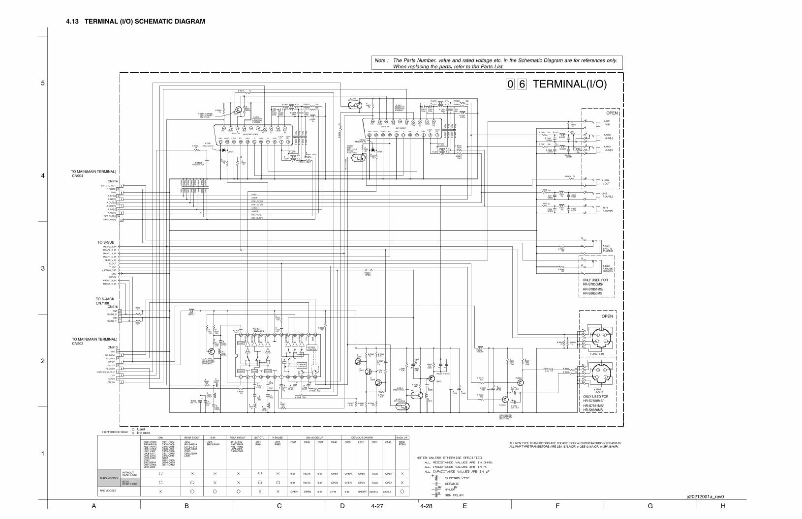
4-27 4-28
1
2
3
5
4
A B C D E F G H
TERMINAL (I/O) SCHEMATIC DIAGRAM4.13
100/16
100/16
OPEN
OPEN
0.01
0.01
0.01
C931
# DIFFERENCE TABLE
EURO MODELSWITH
ARC MODELS
CH+
R901-R908,R909-R916,R931-R947,
C901-C904,
C933-C936,
C905-C908,
C937-C940,
REAR S-OUT
J904R919-R924C913,C914C941,C942C950Q903,Q904L906
S-IN
J903R925,R926
REAR IN/OUT
J911-J914R927,R928R961-R963L921,L922C960-C963
SAT CTL R.PAUSE
J921 J922R964 R965
SW12VDECUP
C915 C943 C928 C948
CE/V-OUT DRIVER
C929 L912
R951,R953C916-C918,
L908-L911,
C920-C927,
C945,C946
L901,L902
L913-L916,L917-L920,
Q901,Q905Q902
Q906-Q909,Q911,Q912
BACK UP
D901,D902J901,J902
IC901
R966
B903,B904
BT901
0.01
OPEN OPEN 0.01 47/16
C949
OPEN
OPEN
OPEN
OPEN
OPEN
OPEN
10/25
10/25
5.6k SHORT 220/6.3 220/6.3
WITHOUTREAR S-OUT
REAR S-OUT
ALL NPN TYPE TRANSISTORS ARE 2SC4081/QRS/ or 2SD1819A/QRS/ or 2PC4081/R/.ALL PNP TYPE TRANSISTORS ARE 2SA1576A/QR/ or 2SB1218A/QR/ or 2PA1576/R/.
REAR1_Y_IN
REAR1_C_IN
J902
REAR2_Y_IN
R906
CN913
R935
R910
R902
C920
C922
L911
R931
R933
L909
R932
R936
Q909
J903
R926
R961
R905
R925
D902
D901
Q905
R962
L907
C915C943
REAR2_C_IN
J916
R923
L903
R963
REAR_V_IN
Y_OUT
C_OUT
FRONT_Y_IN
GND
R907R914
FRONT_C_IN
R915
R912
R913
J913
R964
R965
L913
L914
L915
R90
8
J901
C917
L904
R924
R930
J912L922
J921
J922
J904
L921
L916
C951
R953
Q911
R951
C934 C933
C93
6
C960
R952
L910
Q912
C93
5
C961
L908
C938 C937
C921
C962
C93
9
C94
0
L918
L917
L919
L920
C963
R927
C95
9
C95
7
C946
Q906
C926
C95
8
C95
6
C95
5
C95
4
R937
C95
3
C90
4
C923
C95
2
C927
C931
Q907
R966
R917
CN914
R918
BT901
V_FROM_OSD
C949
Q908
SW12V
R929CN916
C950
R934
C909 C910
IC901
C945
C918C916
C925
R901
R909C905 C906
L902
C911
C90
7
C901 C902
R904
L901
C90
3
J915
Q902
B903
R916
R911
R939
R938
R940
L912
C929
C924
R942
R943
R945
R946R947
R944
R941
C90
8
C928
Q910
C912
R949
R903
Q901
C948
J911
J914
R928
B904
C913 C942
C914
C941
L906
Q904
Q903
R921 R922
R919
R920
10µH
100
75
75
100
470
510
100
75
0
100
75
0
0.01100
75
15µ
0
10µH
10µH
10µH
100
100
100
100
4.7µ
4.7µ
4.7µ
0Ω
0.022
15µ
75
75
4.7µ
47
5.6k
3.3k
330p 330p
470p
5.6k
1µ
470p
330p 330p
33p
470p
470p
4.7µ
4.7µ
4.7µ
4.7µ
75
10
100
470p
47
47
1K
0Ω
0Ω
75
220
100
0.001
100.022
0.022
0.022
75
75330p 330p
1µ
470p
330p 330p
100
0.22µ
470p
1k
75
100
100
10k0.01
4.7k
0
1k
5606.8k
2.7k
3.3k
470p
0.001
330
68
75
0.01 47
0.01
220
390 390
100
100
A.OUT A.OUT
A.INA.IN A.GND
GND GND GND
GND
V.OUT V.GND R/C GND
V.IN V.GND SCRAMBLE[L]
[L]
[R]
[R]
[H]AV2/DECODER
PEMC1177PEMC1019PU59592
GND
I2C_DATA2
I2C_CLK2
SW12V
CH+12V
3.58NTSC[H]/P.ON_P
LI_5V
SCR[H]
P50_I/O
TU_VIDEO
OPEN OPEN
OPEN
2SB1218A/QR/2SA1576A/QR/2PA1576/R/
MTZJ12C-T2
OPEN
MTZJ12C-T2
OPEN
DTC144WU
SHORT
/16
A.OUT[R]
A.IN[R]
A.OUT A.OUT
A.INA.IN A.GND
GNDGNDGNDR/CV.GNDV.OUTGND
GNDV.GNDV.IN FUNC.SW
P50[L]
[L]
[R]
[R]
PEMC1177PEMC1019PU59592
A.IN[L]SHORT
PU60659
PU60659
SHORT
/16
DTC144WUA
OPEN
DTC114TUA
OPEN
OPEN
OPEN
OPEN
OP
EN
OP
EN
/25
OPEN
OP
EN
OP
EN
OP
EN
OP
EN
OP
EN
/16
OP
EN
/16
SAT_CTL_OUT
R.PAUSE
GND
A.IN1[L]
A.IN1[R]
A.OUT[L]
A.OUT[R]
A.IN2[L]
A.IN2[R]
DEC.OUT[L]
DEC.OUT[R]
QVZ0032-001
FRONT_Y
FRONT_C
GND
GND
/6.3
OPEN
BH7636S
/25
OPENA.OUT[L]
2SB1218A/QR/2SA1576A/QR/2PA1576/R/
OPEN
1/2W
UN5211DTC114EUARN1302PDTC114EU
V.IN
V.OUT
/16 /6.3
SHORT
2SB1218A/QR/2SA1576A/QR/2PA1576/R/
1/2W 1/2W
RAPID SW
RAPID SWAV1 IN/OUT
G B
#
#
#
#
#
#
#
#
#
#
#
#
#
#
#
#
#
#
#
#
#
#
#
##
#
#
#
#
#
#
#
#
#
#
##
#
#
BG
#
#
#
##
#
#
#
#
#
#
#
#
##
#
#
#
#
#
#
#
##
#
#
# #
##
#
#
#
#
#
#
#
#
#
#
#
#
#
#
#
#
#
#
#
#
#
##
#
#
# # #
#
#
# #
#
#
#
#
#
#
#
#
#
#
#
#
#
#
#
#
##
#
#
#
#
##
#
#
#
#
#
##
#
#
#
#
#
# #
#
#
TERMINAL(I/O)
TO S-JACKCN7108
TO S-SUB
S-IN
EX
P1
Y
EX
P2
CURRENTLIMITER
SAT.CTL
0
S-OUT
Y
C
21TO MAIN(MAIN TERMINAL)CN903
43
R.PAUSE
C
21
43
AV
1_Y
CIN
[H]
6
CLAMP CLAMP CLAMP
CLAMP
6dB 6dB
CLK
DAT
A
DR
IVE
R
BU
FF
ER
DR
IVE
R
BU
FF
ER
BU
FF
ER
BU
FF
ER
BU
FF
ER
I2C-BUSCONTROL
A.IN[L]
A.IN[R]
TO MAIN(MAIN TERMINAL) CN904
LINE_OUT[R]
LINE_OUT[L]
A.IN2[L]
A.IN2[R]
DEC_OUT[R]
DEC_OUT[L]
Ω
Ω
Ω
Ω
OPEN
OPEN
The Parts Number, value and rated voltage etc. in the Schematic Diagram are for references only.When replacing the parts, refer to the Parts List.
Note :
p20212001a_rev0
: Not used: Used
OPEN
ONLY USED FORHR-S7850MS/
HR-S7851MS/HR-S8850MS
ONLY USED FORHR-S7850MS/
HR-S7851MS/HR-S8850MS

4-29 4-30
DEMODULATOR SCHEMATIC DIAGRAM
HGFEDCBA
4
5
3
2
1
4.14
The Parts Number, value and rated voltage etc. in the Schematic Diagram are for references only.When replacing the parts, refer to the Parts List.
Note :
p20162001a_rev3
LPA10094 LPA10094 LPA10094 LPA10094 LPA10094 LPA10094 LPA10094
FRANCEEU/EK ARC
V13 V14
LPA10094
EU/EKMS
KOREA4SYSTEM
ARC ARC
3SYSTEM
-01* -02* -03* -04* -05* -06* -07* -08*
R6703PRE AMP
DEMOD PWB ASSY
MS
FRANCE
R6705
R6706
C6702
C6703
C6705
L6701
L6702
# DIFFERENCE TABLE
47 47 47 470 0 0 0
270 270 270 270 270 270 270100
150 150 100
0.0022 0.0022 0.0022
220p 220p 180p
0.001 0.001 0.001
1µ 1µ 1µ
3.3µ 3.3µ 3.3µ 3.3µ 3.3µ 3.3µ
SHORT SHORT SHORT SHORT SHORT
MONO IN K6707
C6724
R6718
FE 600 FE 600
0.22/50 0.22/50
I2C-BUS R6708,R6709
K6703,K6704
C6710,C6711
100 100 100
FE 600 FE 600 FE 600
FE 600 FE 600 FE 600 FE 600 FE 600
1K 1K 1K 1K 1K
ANALOG
Vcc
R6707
K6701
C6706
DIGITAL
Vcc
R6710
K6705
C6712
22 47 47 FE 600 FE 600 FE 600 FE 600 FE 600
FE 600 FE 600 FE 600 33 33 33 33 33
10
10 10 10 10 10
FE 600 FE 600 FE 600 FE 600 FE 600
FE 600 FE 600 FE 600
12 12
DAC Vcc R6716
K6706
C6718
47 47 47
47 47 47 47 47
FE 600 FE 600 FE 600 FE 600 FE 600
FE 600 FE 600 FE 600
8p 8p 8p 7p 7p 7p 7p 7p
1p 1p 1p 3p 3p 3p 3p 3p
C6708
C6709
X'TAL
DAC OUT R6713,R6715
C6714,C6716 0.0068 0.0068 0.0068 0.00680.0022 0.0022 0.0022 0.0022
VREF C6722
C6723 0.01 0.01 0.01 0.01 0.01 0.01 0.010.001
IC6701
C6719
C6706
K6701
K6702
C6707
X6701
C6709
C6708
K6703
K6704 R6709
R6708
C6710
C6711
K6705
R6710C6721
C6712
C6713
D6701
R6711
R6712R6714
R6713R6715
C6714C6716 C6715C6717
K6706
R6716C6718
C6720
C6722
C6723C6724
R6707
K6707
CN6701
C6701
R6701
R6702
L6701
C6702
R6703
Q6701
R6705
C6705
R6706
L6702
R6704
C6703
C6704
R6718
R6719
R6720
R6721
10
0.01
600
600
47p
1p
8p
600
600 100
100
100p
100p
600
0.01
0.01
0.22
680k
1k1k
22k22k
0.00680.0068 2.22.2
600
470.01
10
10
0.012.2600
0.01
3.9k
6.8k
1µ
0.0022
47
270
0.001
150
3.3µ
1k
0.01
10k
5.6k
5.6k
MSP3417D
/16
CH CHCH
CH
CH
1SS1331N4148M
/50/50
/16
/16
/50
I2C_DATA
I2C_CLK
TU_A_MUTE
DEMOD_[R]
DEMOD_[L]
SW5V
GND
COMP
SIF
NC
2SC3936/BC
#
#
# #
#
#
# #
#
#
#
#
#
#
##
##
#
##
#
##
#
#
#
#
#
#
#
#
# ##
AV
SU
P
AN
A_I
N1+
AN
A_I
N-
TE
ST
EN
XTA
L_IN
XTA
L_O
UT
TP
D_C
TR
_OU
T1
D_C
TR
_OU
T0
AD
R_S
EL
STA
ND
BY
Q I2C_CL
I2C_DA
TP
TP
TP
TP
TP
DVSUP
DVSS
TP
RESETQ
TP
TP
VR
EF
2
DA
CM
_R
DA
CM
_LTP
VR
EF
1
SC
1_O
UT
_R
SC
1_O
UT
_LNC
AH
VS
UP
CAPL_M
AHVSS
AGNDC
NC
NC
NC
SC1_IN_L
SC1_IN_R
VREFTOP
MONO_IN
AVSS
A GND
D GND
18.432MHz
1 4 DEMOD
TO MAIN (TUNER)CN6701

4-31 4-32
1
2
3
5
4
A B C D E F G H
S-P CONVERTER SCHEMATIC DIAGRAM4.15
# MARKED ELEMENTS ARE NOT MOUNTED.
ABOUT ## MARKED ELEMENTSELEMENTS
MODELSCN1601 CN1602
3pin-6pin
1pin-11pin
3pin-11pin
HR-S6850MS
VR1200/39
HR-S7850MSHR-S8850MS
NOT USED
IC1605
CN1602
Q1601
C1637
CN1601
C1643
C1642
B1601
L1603
C1640
R1623
R1624
C1615
C1641
C1614
C1639
IC1602
L1602
C1635
C1636
D1601
C1612
R1621
R1622
C1651
R1651
IC1606
R1652
C1613
C1638
C1634
C1616
C1608
C1654 C1655
C1645
C1646
R1649
R1650
C1647
C1649C1648
C1650
C1652
R1653
X1601
VR1603
R1654
R1620
R1655
C1653
C1606
C1609
R1618
R1617
C1610
C1611 R1619
R1616
R1615 C1605
C1607
R1646
R1648
Q1605
L1604
Q1614
R1647
R1645
Q1613
C1644
R1633
R1634R1631
R1632
Q1606
C1631
D1602
C1632 C1633
R1612
Q1617
R1661
R1660
C1659
Q1616
IC1604
IC1608
C1661
Q1615
R1659
R1658
R1657R1656 IC1607
C1656
X1602
L1605
C1658
R1601
C1657
C1660
C1663
R1662
R1663
Q1618
R1664
C1664
B1605
B1602
B1603
B1604
CN1603
C1662
Q1607
Q1609
R1638
R1637
R1639
VR1601
Q1610
Q1612
R1635
R1636
R1610
R1609
R1611
L1601
C1602Q1602
Q1603
R1602
R1603
R1605
R1604
R1606
R1608
R1607
C1603FL1601 FL1602
C1601
R1643
R1642
Q1604
Q1608
R1644
VR1602
R1640
R1641
Q1611
IC1603
IC1601
0.01
0.01
0.01
10µ
47
12k
120k
470p
0.01
470p
0.01
10µ
0.1
0.22
0.1
10K
10K
0.022
12k
1k
0.1
47
100p
0.1
47
0.01 47
1
1
0.22
0.0147
0.22
12p
180k 100k
560
3.3k
1.2k
0.22
1000p
2200p
10k
470k
1
100p 130k
470k
330 1
0.01
100k
1k
10µ
1.5k
1.5k
0.01
22k
560
3.3k
47
47 0.01
10k
33k
27k
470
470
680
1k
5602.2k
0.01
10µ
47
3.3k
0.01
0.01
470
10k
10k 1.2k
0.01
1p
100
680
330
470
1.2k
1k
1k
1k
2.7k
10µ
0.01
47k
56k
680
1.2k
680
2.2k
330
22
47
100
680
330
470
1.2k
1k
-(B-Y)
n.c.
n.c.
CVBSfref
TEST
GND
n.c.
SSC
n.c.
CLOCHEref
PLLref
n.c.Vp
n.c.
-(R-Y)
TDA8395
SW12V
SW12V
GND
GND
GND
GND
SW12V
SW12V
FROM_PS_Y
GND
GND
GND
TO_PS_Y
FROM_PSS_C
TO_PS_C
SW5V
SW5V
/6.3
74HC132D
1SS133
A_VCC
A_GND
R-Y_OUT
B-Y_OUT
R-Y_IND_VCC
NC.
NC.
NC.
NC.
IC.
IC.
IC.
B-Y_IND_GND
SSC_IN
TDA4665T
/6.3
/6.3
/6.3
/50
/50
/6.3
QAX0345-001Z
/50
/50
2SC4083/NP/
2SC1740S(QR)
/16
MTZJ7.5A
/16
1CLR
1D
1CK
1PR
1Q
1Q
GND
VCC
2CLR
2D
2CK
2PR
2Q
2Q
74HC74D
GN
D
Vcc
OU
T
XIN
XO
UT
BA4432G
-(R-Y)
MCONTROL
-(B-Y)
H/2
U_OFFSET
RED
VCC
GREEN
GND
BLUE
V_OFFSET VREF
C_OUT
FLT
CVBS
PAL/NTSC
NOTCH
Y+SYNC_OUT
Y+SYNC_IN
BURST_ADJ
Y+SYNC_OUT
OSC
SYNC_IN
TDA8501T/N1-X
QAX0576-001Z
/6.3
/16EQ
QQR1187-001
EQ
QQR1187-001
/16
GND
C/R1
RE1
A1
B1
Q1
Q1
GND
GND
VCC
C/R2
RE2
A2
B2
Q2
Q2
74HC4538D
BA7046F
##
##
#
#
#
#
#
#
#
Y
#
#
##
#
#
#
#
#
#
#
#
#
#
#
#
#
#
#
#
#
#
#
C.SYNC
H.SYNC(-)
WIDE_V.SYNC(-) fH/2
H.SYNC(+)
SSCTO S-SUBCN511
SYNCSEPA
V.SEPA
PHASECOMP
H.OSC
R-Y LEVELADJ.
B-Y LEVELADJ.
FROM/TOMAIN
The Parts Number, value and rated voltage etc. in the Schematic Diagram are for references only.When replacing the parts, refer to the Parts List.
Note :
TO MAIN(CONNECTION)CN6102
OPEN
OPEN
0Ω
0Ω
OPEN
0Ω
p20219001a_rev0
8 7 S-P CONVERTER

4-33 4-34
4.16 MAIN CIRCUIT BOARD
12
12
18
12
825
B
E
B
B
1
117
106
26 1
3
4443
19
1
49
21
EE
3332
B
E
CN
6701
CN
501
X3001
CN
3006
L12
TU
6001
CN
3002
C5352
C7011
R5313
B5001
B5002
B5301
B5302
B5303
C5001
C5002
C5004
C5101
C5106
C5201
C5207
C5301
C5302
C5303
C5304
C5306
C5307
C5309
C5310
D5101
D5103
D5105
D5201
D5203
D5204
D5205
D5208
D5209
D5210
D5211
D5301
D5302
D5303
D5304
D5306
D5308
D5309
D5317
L5201
L5202
LF5002
Q5301
Q5306
Q5307
Q5312
Q5319
R5102
R5104
R5107
R5108
R5301
R5307
R5308
R5314
R5315
R5318
R5324
R5326
R5328
R5329
C3011
C3010
K5301
B203
B206
B3070
B3079
B3179
B3966
B3971
B4001
B7001
C201
C202
C206
C207
C208
C209
C210
C211
C214
C215
C216
C218
C222
C3007
C3014
C3018
C3020
C3021
C3022
C3024
C3026
C3028 C
3029
C3031
C3034
C3035
C3036 C
3041
C3042
C3049
C3054
C4001
C4003
C4005
C4006
C4010
C4011
C4013
C4014
C4016
C6006
C6007
C6008
C6012
C6013
C6016
C6023
C6501
C6502
C7002
C7003
C7005
C7006
C7007
C7008
C7160
C7165
C7166
C7167
D201
D202
D203
D3003
D3004
D3005
D3006
D4002
D6002
D7002
L203
L204
L6003
Q207
Q208
Q3007
Q4001
Q6032
R202
R203
R204
R208
R209
R211
R212 R
213
R216
R220
R3017
R3018
R3020
R3021
R3022
R3025
R3026
R3029
R3030
R3031
R3032
R3033
R3039R
3040R
3041
R3042
R3055
R3056
R3057
R3058
R3066
R3069
R3071
R3078
R3079
R3080
R3085
R3086
R3088
R3089
R3090
R3091R
3092R
3093
R3096R
3103R
3105
R3205
R3206
R3207
R3211
R3214R
3215R
3216
R3220
R3222
R3225
R3229
R3230
R3231
R3233
R3234
R3237
R3238
R3239
R3240
R3241
R3242
R3246
R3247
R3252
R4005
R4007
R4008
R4009
R4010
R4011
R4012
R4013
R4015
R4017
R4018
R4019
R4020
R6030 R
6031
R7007
R7008
R7010
R7011
R7012
R7013
R7014
R7016 R
7017
R7018
R7161
R7162
R7203
Q5322
R5344
CP
3002
R4021
Q5323
W205
W1205
W802
W1403
W1
W2001
W211
W203
W202
B6511
B302
B42
B2051
C2
C4
C5
C7
C8
C9
C13C
14
C16
C17
C20
C24
C26
C27
C30
C31
C34
C35
C44
C60
C61
C64
C72
C73
C74
C76
C78
C324
C80
C84
C93
C103
C106
R40
C124
C303
C304
C305
C308
C309
C310 C
314
C315
C316
C319
C321
C322
C401
C402
C403
C405
C407
C409
C2002
C2003
C2004
C2005
C2006
C2007
C2008
C2010
C2011
C2051
C2052
C2053
C2054
C2064
C2201
C2203
C2206C
2207
C2208
C2210 C
2211
C2212
C2214
C2216
C2219
C2220
C2227
C2229 C
2230
C2251
C2252
C2255
C3001
C3003
C3004
K2251
K2252
K2253
L2
L5
L11
L18
L24
L301
L27
L2251L3001
Q1
Q5
Q8
Q14
Q16
Q17
Q28
Q303
Q38
Q39
Q40Q
302
Q403
Q404
Q405
Q2001
Q2002
Q2003
Q2004
Q2062 Q
2063
Q2251
Q2252
R2
R3
R4
R7
R8
R21
R22
R23
R26
R27
R28
R30
R33
B52
R36
R39
R42
R46
R51
R62
R75
R79
R317
R88
R90
R92
R104
R117R
301
R302
R304
R306
R307 R
308R309
R310
R313
R315
R316
R329
R401
R402
R404
R405
R406
R408
R2006
R2007
R2008
R2009
R2014
R2017
R2020
R2021
R2051
R2053
R2054R
2055
R2057
R2059
R2063
R2064
R2065
R2201
R2202
R2203
R2211 R
2213
R2217
R2218
R2219
R2220R
2222
R2224
R2225
R2227
R2228
R2251
R3204
R327
R328
Q311
B301
R321
R326
R226
W18
W6
W5
W9
W14
W4
L31
W15
B12
B214
C142
C47
L30
R41
C46
C5351
R111
C56
R3106
CP
3003
K2001
K2002
K2003
K2004
B55
C140
C141
B65
W17
POWER
23
2
1363
5
1
13
12
51532
SUPPLY
2
1
PAUSE
1
41
111
1210
3435
8
STARTSENSOR
CH+
TEST
CH- REC MENUOK
1
B
34
1
1
61
90
30
31
EB
16
AUDIOIN[R]
AUDIOIN[L]
VIDEOIN
REC.S
8
4
SENSOREND
D.FF
CTL.P
PB.FM
A.PB.FM
2
1
4
87
4
51
91
TAKE UP
4
8485
56
57
29
1
112
28
E
EB
8
1
4 2
S.CASS
8
19
2
21
6 2
51
5
1
9
30
A
5 1
1
BROWNBLUE
91
S-ET
SAT
SAT
PLAY STOP/EJECT PAUSE REC
E PROG
5
4
1
15
14
28
6
71
2
1
6
4
120
13
4 1
23
1
2
110 110 1 12
64
30
3
8 5
41
15
B E
V2
FF REW
60
DI7001
CN901 CN902 CN903
R4006
D3001
PC3002
Q3002
PC3001
D5318
CP4002
TP106
Q3003
S3001
IC301
CN3004
TP111
X3002
D7008
S7002
S7004
S7001
IC1
C3025
IC3001
CN3001
J7105S7010S7013
S7015 S7014
S7012
S7011 S7006S7008
IC7001
TP4001
CN7001
IC7003
P
P
S7016P
D7009
S3002
TP2253
P
CN1
IC201
CN2002CN3003
CN904
PP
CN2001
L4001
C4031
R5312
PC5101
F5001
T5001
B5304
C5006
C5102
C5103
C5104
C5105
C5107
C5202
C5203
C5204
C5206
C5208
C5305
C5308
C5311
CP5302
D5001
D5102
D5206
D5305
D5307
D5310
D5316
FC5001 FC5002
IC5301
K5101
K5102
LF5001
Q5101
Q5102
Q5302
Q5303
Q5304Q5305
Q5308
Q5309
Q5310
Q5311
Q5318
Q5320
R5101
R5103
R5106
R5109R5110
R5111R5112
R5302R5303
R5304
R5305R5306
R5309 R5310R5311
R5316
R5317
R5319
R5320
R5321
R5322R5323
R5325
R5327
R5330
R5332
VA5003
CN5001
IC3002
IC3003
TPGNDTP7001
CN3901
D5202
C5205B204
B3962
C204
C212
C213
C217
C2061
C3008
C3012
C3015C3016
C3017
C3027
C3030
C3032
C3033
C3037
C3038
C3039
C3040
C3050
C4002
C4004
C4007
C4008
C4009
C4012
C4015
C4017
C6005
C6020C6021
C6027C6028C6032C6037
C6052C6053
C6055
C7001
C7004
C7009
C7010
C7202
CP4001
D3002
D3008
D4001
D7001D7003
D7004
D7005
D7006
D7007
K6080
L201
L202
L206
L6001
L7201
Q3004
Q3005
Q3901
Q4002
Q4003
Q6030
Q6031
Q7201
R201R210
R224R225
R3011R3012
R3013
R3014
R3015
R3016
R3019
R3027
R3034R3035
R3036
R3038 R3044
R3046
R3047
R3048
R3049
R3050
R3051R3052
R3053
R3054
R3059
R3060
R3061
R3062R3063
R3072
R3073R3074R3075
R3076 R3077
R3081
R3083
R3087
R3094
R3095
R3097
R3104
R3208
R3209
R3210
R3212
R3213R3217
R3218
R3219
R3223R3224
R3235R3236
R4001
R4003R4004
R4016
R6020
R6021
R6032
R6033
R6050
R6051
R6052
R7001
R7002
R7003R7004
R7005
R7006
R7009
R7015
R7160
R7163
R7202
R7204
R5345
CP5301
L5301
W801
B6510
W16
W12
W2
C6
C2231
IC3004
B3
B8
B9
B25
B50
C1
C3
C10
C11
C12
C15
C19
C21
C22
C23
C25
C28
C29
C32
C33
C36C37
C38
C39
C40
C45
C59
C63
C65
C69
C70
C71
C75
C77
C82
C323C108
C109
C110
C112C114
C301
C302
C306C307
C311
C312
C313C317
C318
C320
C404
C406
C2001
C2009
C2012
C2013
C2014
C2015
C2055
C2062
C2063
C2202
C2204C2205
C2209
C2213
C2215C2217
C2218
C2221
C2222
C2223C2224
C2225
C2226
C2228
C2253C2254
C3002
D1
D6D8
D2201
D2202
IC2
L1
L3
L4
L13
L304
L15
L17
L19
L20
L28
L302
L303
L401
L402
L2001
L2252
L3011 L3012
Q2
Q3
Q4
Q6Q7
Q9
Q10
Q11
Q18
Q21
Q24
Q25
Q41
Q301
Q401
Q402
Q2005
Q2051
Q2052Q2053
Q2054
Q2055
Q2061
R1
R5 R6
R9
R24
R25 R29
R31 R32
R35
R37
R318
R48
R54
R65 R68
R70
R77
R91
R93
R113
R303R305
R311 R312
R314
R403
R407
R2001R2002R2003
R2005
R2010
R2013
R2015
R2016R2018
R2019
R2052
R2056
R2058
R2060
R2061
R2062
R2204
R2205
R2206
R2208 R2209
R2210
R2215
R2223 R2226
R2229
R3201
R3202
R3203
T2051
T2052
X1
X2
Q312
Q3001
W13 W11 W10 W8
W3
C143
CN905
W7
C5003
B13
D5319
D11
IC4
R118
C225
Q26
B3279
R38
ZZ1
ZZ2
ZZ3
ZZ4
ZZ5
ZZ6
ZZ7
ZZ8
ZZ9
C4032
C139
CP5304
CP5303
C2016Q2006R2022
R2023 C2017
C6056
<03> MAINLPB10140-001A
DANGEROUS VOLTAGE

4-35 4-36
2D DIGITAL AND 3D DIGITAL/2M CIRCUIT BOARDS4.17REF.NO. LOCATION REF.NO. LOCATION REF.NO. LOCATION REF.NO. LOCATION REF.NO. LOCATION REF.NO. LOCATION REF.NO. LOCATION REF.NO. LOCATION REF.NO. LOCATION
CAPACITOR
C1 B C 14NC2 B C 14NC3 B C 14NC4 B C 14OC5 A D 15NC6 A D 13NC7 B C 14PC8 B C 14PC9 A D 9NC10 B C 12NC11 B C 11OC12 B C 11OC13 B C 11NC14 B C 11NC15 B C 11NC16 B C 11NC17 A D 10NC19 A D 10MC20 A D 9MC21 B C 11MC22 A D 11MC23 B C 11NC24 A D 10MC25 B C 11MC26 B C 11LC27 B C 10MC28 A D 10MC29 B C 11LC30 B C 10LC31 A D 10LC32 A D 11LC33 A D 11LC34 B C 10LC35 B C 11KC36 A D 11KC37 A D 12KC38 A D 11KC39 B C 12KC40 A D 12JC44 B C 15NC45 A D 12LC46 B C 11KC47 A D 10MC56 B C 10KC59 B C 8MC60 A D 7MC61 B C 12OC63 B C 10NC64 B C 9LC65 A D 12OC69 B C 16NC70 B C 16NC71 B C 8LC72 B C 8LC73 B C 7MC74 B C 7MC75 B C 8LC76 B C 9KC77 B C 8KC78 B C 8KC80 B C 10MC82 B C 10NC84 B C 11OC93 B C 8LC103 B C 8LC106 B C 10NC108 B C 10KC109 B C 10OC110 B C 10NC112 B C 10KC114 B C 10KC124 B C 8KC139 B C 11OC140 B C 11JC141 A D 7HC142 B C 20HC143 A D 12LC201 A D 20GC202 B C 19GC204 B C 19GC206 B C 19GC207 B C 19GC208 B C 18GC209 B C 18HC210 B C 18GC211 B C 18GC212 B C 18GC213 A D 18FC214 B C 18GC215 B C 18GC216 A D 17HC217 B C 19HC218 A D 19HC222 B C 19GC225 A D 17FC301 B C 7KC302 B C 7KC303 B C 7JC304 B C 7JC305 B C 7KC306 B C 7KC307 B C 6KC308 B C 6LC309 B C 6JC310 B C 6JC311 B C 6JC312 B C 6JC313 B C 6JC314 B C 6J
C315 B C 6JC316 B C 6JC317 B C 6JC318 B C 7JC319 B C 7IC320 B C 8JC321 B C 7JC322 B C 7JC323 A D 7LC324 B C 6KC401 B C 15OC402 B C 15OC403 B C 15OC404 B C 16OC405 B C 16OC406 B C 16OC407 B C 16OC409 A D 17OC2001 A D 13KC2002 A D 14LC2003 A D 14NC2004 B C 14NC2005 A D 13NC2006 B C 13OC2007 A D 13OC2008 A D 13OC2009 B C 13OC2010 B C 13OC2011 A D 12OC2012 A D 12OC2013 B C 13NC2014 B C 12KC2015 B C 13OC2016 B C 13OC2017 A D 11OC2051 B C 9OC2052 A D 9OC2053 B C 10PC2054 B C 9PC2055 A D 10OC2061 A D 19KC2062 B C 6MC2063 B C 6LC2064 A D 6LC2201 B C 12KC2202 B C 12KC2203 A D 12KC2204 A D 11KC2205 A D 13KC2206 A D 13JC2207 A D 12JC2208 A D 13KC2209 A D 13KC2210 A D 13KC2211 A D 14KC2212 A D 14KC2213 A D 13LC2214 A D 14LC2215 A D 13LC2216 A D 13LC2217 A D 13LC2218 A D 14LC2219 A D 15LC2220 A D 15LC2221 B C 14MC2222 A D 15LC2223 A D 15LC2224 B C 15LC2225 A D 15LC2226 A D 14MC2227 B C 14MC2228 B C 14MC2229 B C 13LC2230 B C 15KC2231 B C 12LC2251 A D 14NC2252 B C 14NC2253 B C 15NC2254 B C 15NC2255 B C 16MC3001 B C 7NC3002 B C 6MC3003 A D 6MC3004 B C 6LC3007 B C 4IC3008 B C 19JC3010 A D 2DC3011 A D 2DC3012 A D 6BC3014 A D 8EC3015 B C 10EC3016 B C 12EC3017 B C 13EC3018 B C 13DC3020 B C 13EC3021 B C 13EC3022 B C 19EC3024 B C 13FC3025 A D 13FC3026 B C 13FC3027 A D 14EC3028 A D 13EC3029 A D 13EC3030 A D 14EC3031 B C 14FC3032 B C 11GC3033 B C 10FC3034 B C 13GC3035 B C 13GC3036 B C 12FC3037 B C 13F
C3038 B C 11GC3039 B C 11GC3040 B C 12DC3041 B C 13FC3042 A D 4DC3049 B C 11DC3050 B C 12FC3054 B C 14FC4001 A D 8EC4002 B C 10EC4003 B C 9DC4004 A D 8GC4005 B C 8FC4006 A D 8GC4007 B C 9EC4008 B C 9EC4009 B C 9DC4010 B C 8FC4011 B C 10GC4012 B C 10HC4013 B C 10FC4014 B C 10FC4015 B C 9EC4016 A D 9GC4017 B C 9GC4031 A D 19MC4032 B C 20NC5001 A D 1PC5002 A D 2NC5003 A D 4PC5004 A D 1JC5006 A D 2MC5101 A D 2MC5102 A D 2KC5103 B C 3LC5104 A D 3MC5105 A D 3LC5106 A D 3KC5107 A D 3KC5201 A D 1HC5202 A D 3GC5203 A D 2GC5204 A D 3HC5205 A D 2HC5206 A D 2FC5207 A D 2FC5208 A D 3GC5301 A D 3EC5302 A D 3EC5303 A D 4EC5304 A D 2EC5305 A D 3FC5306 A D 4GC5307 A D 3EC5308 A D 3EC5309 A D 4EC5310 A D 5FC5311 B C 1EC5351 A D 1FC5352 A D 1FC6005 A D 21MC6006 B C 21MC6007 A D 21NC6008 B C 21MC6012 A D 21PC6013 B C 21PC6016 B C 22OC6020 B C 22NC6021 B C 22NC6023 B C 21MC6027 B C 22LC6028 B C 22LC6032 B C 21LC6037 A D 21LC6052 B C 22OC6053 B C 22PC6055 B C 22OC6056 B C 22PC6501 A D 22GC6502 B C 22GC7001 A D 7BC7002 A D 11AC7003 A D 9BC7004 B C 8AC7005 B C 11BC7006 B C 11BC7007 A D 14BC7008 B C 13AC7009 A D 12CC7010 A D 11AC7011 A D 13BC7160 B C 19BC7165 B C 19AC7166 B C 20BC7167 B C 20AC7202 A D 19N
CONNECTOR
CN1 A D 14OCN501 A D 21HCN901 A D 6PCN902 A D 10PCN903 A D 14PCN904 A D 17PCN905 A D 20PCN2001 A D 9OCN2002 A D 19LCN3001 A D 20MCN3002 A D 7NCN3003 A D 7LCN3004 A D 9F
CN3006 A D 3DCN3901 A D 8BCN5001 A D 1PCN6701 A D 22FCN7001 A D 2C
DIODE
D1 B C 16PD6 A D 13JD8 B C 9JD11 B C 10KD201 A D 19FD202 A D 19FD203 A D 18FD2201 A D 12JD2202 A D 12JD3001 A D 12HD3002 A D 7FD3003 A D 6CD3004 A D 5CD3005 A D 5CD3006 A D 5DD3008 B C 11DD4001 A D 10HD4002 A D 10HD5001 B C 2MD5101 A D 1MD5102 A D 2KD5103 A D 3KD5105 A D 3KD5201 A D 1ID5202 A D 3HD5203 A D 3ID5204 A D 3ID5205 A D 3ID5206 A D 2HD5208 A D 2ID5209 A D 4HD5210 A D 4HD5211 A D 1HD5301 A D 3ID5302 A D 3FD5303 A D 2ED5304 A D 2ED5305 A D 2FD5306 A D 4DD5307 A D 4GD5308 A D 4DD5309 A D 1ED5310 A D 2ED5316 A D 5GD5317 A D 5ED5318 A D 6GD5319 A D 5GD6002 A D 22OD7001 A D 15AD7002 A D 8AD7003 A D 10AD7004 A D 7AD7005 A D 6AD7006 A D 5AD7007 A D 2BD7008 A D 16AD7009 A D 16A
IC
IC1 B C 12MIC2 B C 8LIC4 B C 8HIC201 A D 19GIC301 A D 7JIC3001 B C 11FIC3002 B C 14FIC3003 B C 20EIC3004 A D 5MIC5301 A D 4FIC7001 B C 12BIC7003 A D 8A
JACK
J7105 A D 20A
COIL
L1 A D 16NL2 A D 12OL3 A D 9ML4 A D 10LL5 A D 12KL11 A D 11ML12 A D 11LL13 A D 9LL15 A D 7NL17 A D 8LL18 A D 8LL19 A D 7ML20 A D 11NL24 A D 10NL27 A D 10LL28 A D 10NL30 A D 11KL31 A D 20HL201 A D 20HL202 A D 20GL203 A D 19FL204 A D 17HL206 A D 18HL301 A D 7KL302 A D 6KL303 A D 6JL304 A D 6KL401 A D 16OL402 A D 16OL2001 A D 16M
L2251 A D 15ML2252 A D 15ML3001 A D 6ML3011 A D 6NL3012 A D 7NL4001 A D 19ML5201 A D 3GL5202 A D 2FL5301 A D 4DL6001 A D 21NL6003 A D 21OL7201 A D 18N
TRANSISTOR
Q1 B C 14NQ2 B C 15NQ3 B C 14OQ4 B C 14OQ5 B C 8MQ6 B C 8MQ7 B C 8MQ8 B C 7MQ9 B C 7MQ10 B C 11KQ11 B C 11LQ14 B C 8KQ16 B C 11OQ17 B C 11OQ18 B C 10NQ21 B C 9LQ24 B C 10JQ25 B C 10KQ26 B C 10KQ28 B C 9NQ38 B C 9NQ39 B C 10KQ40 B C 10KQ41 B C 9KQ207 B C 18HQ208 B C 18HQ301 B C 6KQ302 B C 8JQ303 B C 6KQ311 B C 7JQ312 B C 8KQ401 B C 15OQ402 B C 16OQ403 B C 17OQ404 B C 16NQ405 B C 16OQ2001 B C 12OQ2002 B C 13OQ2003 B C 12OQ2004 B C 13OQ2005 B C 14OQ2006 B C 10OQ2051 B C 10PQ2052 B C 10PQ2053 B C 11PQ2054 B C 11PQ2055 B C 11PQ2061 B C 6MQ2062 B C 6MQ2063 B C 7MQ2251 B C 15MQ2252 B C 16MQ3001 B C 5MQ3002 A D 4IQ3003 A D 19IQ3004 B C 6CQ3005 B C 6CQ3007 B C 11DQ3901 B C 14EQ4001 B C 8FQ4002 B C 9GQ4003 B C 9GQ5101 A D 2LQ5102 A D 3LQ5301 A D 4GQ5302 A D 2EQ5303 B C 2EQ5304 A D 4EQ5305 B C 3EQ5306 B C 3FQ5307 A D 3FQ5308 B C 4HQ5309 A D 4FQ5310 B C 4EQ5311 B C 5GQ5312 A D 1FQ5318 B C 2FQ5319 B C 1EQ5320 B C 5EQ5322 B C 5GQ5323 A D 3GQ6030 B C 21KQ6031 B C 21KQ6032 B C 22GQ7201 A D 19N
RESISTOR
R1 B C 12NR2 B C 11OR3 B C 11OR4 B C 9MR5 B C 10MR6 B C 10MR7 B C 11LR8 B C 11JR9 B C 13JR21 B C 16OR22 B C 16N
R23 B C 8MR24 B C 8LR25 B C 7MR26 B C 7MR27 B C 8MR28 B C 8LR29 B C 8MR30 B C 7MR31 B C 7MR32 B C 7MR33 B C 11NR35 B C 11OR36 B C 11JR37 B C 11KR38 B C 11LR39 B C 10KR40 B C 10KR41 B C 10KR42 B C 10KR46 B C 9LR48 A D 10LR51 B C 11JR54 B C 10NR62 B C 10NR65 B C 8KR68 B C 8KR70 B C 10NR75 B C 11NR77 B C 14PR79 B C 12KR88 B C 11JR90 B C 11NR91 B C 9JR92 B C 10NR93 B C 10NR104 B C 10NR111 B C 10LR113 B C 11OR117 B C 10KR118 B C 12KR201 B C 20GR202 B C 18FR203 B C 18FR204 B C 18FR208 B C 19FR209 B C 18GR210 B C 17GR211 B C 18GR212 B C 18HR213 A D 19HR216 B C 19GR220 B C 19HR224 B C 18HR225 B C 18HR226 B C 20FR301 B C 7KR302 B C 7KR303 B C 6KR304 B C 7KR305 B C 6KR306 B C 7JR307 B C 6KR308 B C 6JR309 B C 6JR310 B C 6JR311 B C 7JR312 B C 7JR313 B C 8JR314 B C 8JR315 B C 8JR316 B C 7JR317 B C 6LR318 B C 6KR321 B C 7KR326 B C 7JR327 B C 7JR328 B C 6JR329 B C 7JR401 B C 15OR402 B C 16OR403 B C 16OR404 B C 16OR405 B C 16OR406 B C 16OR407 B C 16NR408 B C 17OR2001 B C 14JR2002 B C 14KR2003 B C 14KR2005 B C 15KR2006 B C 15KR2007 B C 15KR2008 B C 14LR2009 B C 14LR2010 B C 14LR2013 B C 13OR2014 B C 13OR2015 B C 13OR2016 B C 13OR2017 B C 13OR2018 B C 12OR2019 B C 12OR2020 B C 13OR2021 B C 13OR2022 B C 10OR2023 B C 10OR2051 B C 9OR2052 B C 9OR2053 B C 9OR2054 B C 10PR2055 B C 9P
R2056 B C 10PR2057 B C 11PR2058 B C 11PR2059 B C 11PR2060 B C 11PR2061 B C 6MR2062 B C 6LR2063 B C 6MR2064 B C 7MR2065 B C 7MR2201 A D 13JR2202 B C 14KR2203 B C 13KR2204 B C 14KR2205 B C 14KR2206 B C 14KR2208 B C 13KR2209 B C 14KR2210 B C 13LR2211 B C 14KR2213 B C 15KR2215 B C 14LR2217 B C 15KR2218 B C 15LR2219 B C 15LR2220 B C 15LR2222 B C 15KR2223 B C 14LR2224 B C 15LR2225 B C 15LR2226 B C 15LR2227 B C 14LR2228 B C 12KR2229 B C 12KR2251 B C 16MR3011 B C 9DR3012 B C 9DR3013 B C 10ER3014 B C 9DR3015 B C 10DR3016 B C 10DR3017 B C 9DR3018 B C 9DR3019 B C 10DR3020 B C 10DR3021 B C 10DR3022 B C 10DR3025 B C 11DR3026 B C 11DR3027 B C 9CR3029 B C 11DR3030 B C 11DR3031 B C 11DR3032 B C 11DR3033 B C 11DR3034 B C 9CR3035 B C 9CR3036 B C 9CR3038 B C 12DR3039 B C 12DR3040 B C 12DR3041 B C 12DR3042 B C 14CR3044 B C 15DR3046 B C 13DR3047 B C 12ER3048 B C 14DR3049 B C 12ER3050 B C 12ER3051 B C 12ER3052 B C 13ER3053 B C 12ER3054 B C 15DR3055 B C 13ER3056 B C 13ER3057 B C 14ER3058 B C 14ER3059 B C 14ER3060 B C 13FR3061 B C 13FR3062 B C 14ER3063 B C 14ER3066 B C 13FR3069 B C 12FR3071 B C 14FR3072 B C 14FR3073 B C 14FR3074 B C 12GR3075 B C 12GR3076 B C 12GR3077 B C 13GR3078 B C 12GR3079 B C 12GR3080 B C 11GR3081 B C 12GR3083 B C 11GR3085 B C 11GR3086 B C 11GR3087 B C 12GR3088 B C 11GR3089 B C 11GR3090 B C 11GR3091 B C 10GR3092 B C 10GR3093 B C 10GR3094 B C 10IR3095 B C 14JR3096 B C 10GR3097 B C 10IR3103 B C 9GR3104 B C 9G
R3105 B C 9GR3106 B C 9GR3201 B C 5MR3202 B C 5MR3203 B C 5MR3204 B C 5NR3205 A D 12IR3206 B C 8DR3207 A D 17DR3208 B C 16ER3209 B C 16ER3210 B C 8GR3211 B C 8GR3212 A D 7FR3213 B C 8DR3214 B C 8DR3215 B C 8DR3216 B C 8DR3217 A D 7DR3218 A D 6ER3219 B C 6CR3220 B C 6CR3222 B C 6BR3223 B C 20ER3224 B C 20ER3225 B C 17DR3229 B C 12FR3230 B C 13FR3231 B C 14FR3233 B C 14CR3234 B C 11DR3235 B C 7CR3236 B C 7CR3237 B C 6BR3238 B C 6BR3239 B C 21ER3240 B C 21ER3241 A D 7BR3242 B C 9DR3246 B C 10DR3247 B C 10DR3252 B C 9DR4001 B C 9HR4003 B C 9ER4004 B C 9ER4005 B C 9ER4006 B C 9ER4007 B C 9ER4008 B C 11DR4009 B C 10GR4010 B C 10GR4011 B C 10HR4012 B C 10GR4013 B C 9FR4015 B C 9HR4016 B C 10GR4017 B C 10FR4018 B C 10FR4019 B C 10GR4020 B C 9GR4021 B C 9GR5101 A D 3MR5102 A D 3MR5103 A D 3MR5104 A D 1LR5106 A D 1LR5107 A D 3KR5108 B C 3LR5109 A D 3LR5110 B C 2LR5111 B C 3KR5112 B C 3KR5301 B C 4HR5302 B C 4HR5303 B C 4HR5304 B C 4IR5305 B C 2ER5306 B C 2ER5307 B C 4HR5308 B C 2ER5309 B C 2ER5310 B C 4ER5311 B C 3ER5312 B C 2FR5313 B C 3FR5314 B C 4FR5315 B C 3FR5316 B C 4FR5317 B C 4HR5318 A D 1FR5319 B C 3ER5320 B C 4HR5321 B C 4FR5322 B C 4ER5323 B C 4ER5324 B C 4GR5325 A D 4GR5326 A D 1FR5327 B C 1FR5328 B C 1FR5329 B C 2FR5330 B C 1HR5332 A D 3HR5344 B C 3GR5345 A D 4GR6020 B C 21NR6021 B C 21NR6030 B C 21KR6031 B C 21KR6032 B C 21LR6033 B C 21L
R6050 A D 21OR6051 B C 21PR6052 B C 21OR7001 B C 11AR7002 B C 11BR7003 B C 11BR7004 B C 11BR7005 B C 11BR7006 B C 11BR7007 A D 14BR7008 A D 14BR7009 A D 3AR7010 B C 8AR7011 B C 11AR7012 B C 10AR7013 B C 11BR7014 B C 10BR7015 A D 11BR7016 B C 7BR7017 B C 15AR7018 B C 15AR7160 B C 19BR7161 B C 19AR7162 B C 20BR7163 B C 21BR7202 B C 18NR7203 B C 19NR7204 A D 18N
SWITCH
S3001 A D 18CS3002 A D 6FS7001 A D 22BS7002 A D 18BS7004 A D 7BS7006 A D 6BS7008 A D 5BS7010 A D 4BS7011 A D 4BS7012 A D 3BS7013 A D 2BS7014 A D 2BS7015 A D 1BS7016 A D 17B
TEST POINT
TP106 A D 20KTP111 A D 20LTP2253 A D 20KTP3901 B C 12DTP3902 B C 12ETP3903 B C 13ETP3904 B C 14FTP3905 B C 13FTP3906 B C 13ETP3907 B C 14ETP3908 B C 14ETP4001 A D 20KTP7001 A D 3ATPGND A D 4A
OTHER
CP3002 A D 5JCP3003 B C 5JCP4001 A D 19MCP4002 B C 18MCP5301 A D 4DCP5302 A D 4GCP5303 B C 4DCP5304 B C 4GDI7001 A D 12AF5001 A D 2PFC5001 A D 2PFC5002 A D 3PK2001 B C 13NK2002 B C 13NK2003 B C 9OK2004 B C 9OK2251 B C 15NK2252 B C 15NK2253 B C 15NK5101 A D 2KK5102 A D 1NK5301 A D 4GK6080 B C 21NLF5001 A D 4PLF5002 A D 3NPC3001 A D 16FPC3002 A D 8GPC5101 A D 4MT2051 A D 9OT2052 A D 6LT5001 A D 1KTU6001 A D 22PVA5003 A D 2OX1 A D 11LX2 A D 11LX3001 A D 13FX3002 A D 13F
COMPONENT PARTS LOCATION GUIDE <MAIN>
LPB10090-001B<05> 2D DIGITAL [HR-S6850MS/S7850MS/S7851MS]
22
LEVELD/A
ADJ
1
12
11
1
34
44
33
23
2D DIGITAL PWB
12
17
LPB10090 -001B
IC1201
B1201
B1202
C1201
C1202
C1203C1204
C1206
C1208
C1209
C1211
C1212C1213
C1214
C1215
C1216
C1217
C1218C1219
C1220
C1221C1223 C1226
C1227
C1228
R1224C1230
C1236C1237
CN1201
D1201
L1202
L1203
L1204
L1205 L1206
L1207
LC1201Q1202
Q1203
R1201
R1202
R1203
R1204R1206
R1207
R1210
R1212
R1218 R1219
VR1201
C1239C1240 C1242R1221
R1229 C1249C1244
D1202
D1203R1223
C1243
C1246
C1247
C1245
C1229
R1228
R1225 R1226R1230R1231
R1232
C1250
50
LPA10090
EB
2D D
IGITAL PW
B ASS'Y
C1205
C1207
C1210
C1222
C1224C
1225
C1231
C1232 C
1233
C1234
C1235
L1201
Q1201
R1205
R1208
R1209
R1211
R1213
R1214 R
1215
R1216
R1217
B1203C
1238
C1241L1208 L1209
R1220
R1222
Q1204
B1204
W1241
Q1205
Q1206
R1227
C1248
R1233
<05> 3D DIGITAL/2M [HR-S8850MS]LPB10105-001B
61
801
20
21
4041
0 5
LEVELADJ
PWB Ass'Y3D DIGI/2M
LPA10105
117
60
3D DIGI/2M PWB
LPB10105-001B
IC1401
C1446
C1403
C1416
C1410
C1451
C1442
B1409
Q1421
Q1422D1404
C1402
C1404
C1407 C1408
Q1418
C1420
C1421
C1422 C1423
C1424
C1427
C1437
C1438C1439
C1443
C1447
C1449
C1450
C1453
C1454
C1466
C1468 C1470
C1473
CN1401
D1401
L1401
L1402
L1403
L1405
L1406
L1409
Q1403
Q1406
Q1407
Q1408
Q1412
Q1414
R1404
R1405
R1413
R1421
R1431
R1436
R1437
R1438
R1439
R1441
R1442
R1455
VR1401
R1461
Q1419
D/A
BE
C1429
C1448
C1401
C1432
Q1420
B1412
D1403
C1405
C1406
C1409
C1411
C1412
C1413C
1414
C1415 C
1417
C1425
C1426
C1428
C1430
Q1417
C1433
C1434
C1435
C1436
C1440
C1441
C1444
C1445
C1452
C1455
C1459
C1460
C1461
C1462
C1463
C1464
C1465
C1467
C1469
C1471
C1472
D1402
L1404
L1407
LC1401
LC1402
Q1401
Q1402
Q1404
Q1410
Q1413
R1401
R1402
R1406
R1407
R1408
R1410
R1411
R1412
R1414
R1415
R1416
R1417
R1418
R1425 R
1426
R1427
R1428
R1429
R1430
R1432
R1433
R1434
R1435
R1440
R1446
R1447
R1448
R1449
R1450
R1451
R1452
R1453
R1454
R1462
R1463
R1458
W1401
W1402
R1459
B1416
R1460
COMPONENT PARTS LOCATION GUIDE <3D DIGITAL/2M>
COMPONENT PARTS LOCATION GUIDE<2D DIGITAL>
REF.NO. LOCATION REF.NO. LOCATION REF.NO. LOCATION
CAPACITOR
C1201 A D 5DC1202 B C 5CC1203 B C 1AC1204 B C 1AC1205 B C 2AC1206 B C 3AC1207 B C 4AC1208 B C 4AC1209 B C 4AC1210 B C 6BC1211 A D 2EC1212 B C 2DC1213 B C 2DC1214 B C 2DC1215 A D 2DC1216 B C 3DC1217 B C 2CC1218 B C 2CC1219 B C 3CC1220 A D 3BC1221 B C 2BC1222 B C 2BC1223 B C 2BC1224 B C 3BC1225 B C 3BC1226 B C 2BC1227 B C 3CC1228 A D 3BC1229 B C 4CC1230 B C 4CC1231 B C 4CC1232 B C 4CC1233 A D 4CC1234 B C 4DC1235 A D 4DC1236 B C 4DC1237 B C 3DC1238 B C 4B
C1239 B C 5BC1240 B C 5BC1241 B C 5BC1242 A D 5BC1243 B C 2AC1244 A D 3BC1245 B C 5BC1246 A D 5CC1247 B C 5CC1248 B C 4AC1249 B C 5BC1250 B C 5A
CONNECTOR
CN1201 A D 5A
DIODE
D1201 A D 5CD1202 A D 2AD1203 A D 3A
IC
IC1201 B C 3D
COIL
L1201 A D 5AL1202 A D 3EL1203 A D 4DL1204 A D 4BL1205 A D 2BL1206 A D 3BL1207 A D 4DL1208 A D 4BL1209 A D 5B
TRANSISTOR
Q1201 A D 5CQ1202 B C 2BQ1203 B C 3BQ1204 B C 4BQ1205 B C 3C
Q1206 B C 4B
RESISTOR
R1201 B C 5CR1202 B C 5CR1203 B C 1AR1204 B C 1AR1205 B C 2AR1206 B C 5AR1207 B C 2DR1208 B C 2DR1209 B C 2DR1210 B C 3BR1211 B C 2CR1212 B C 2BR1213 B C 1BR1214 B C 2BR1215 B C 3BR1216 B C 2BR1217 B C 2BR1218 B C 3CR1219 B C 4CR1220 B C 4AR1221 B C 4BR1222 B C 4BR1223 B C 1BR1224 B C 4CR1225 B C 4AR1226 B C 4AR1227 B C 4BR1228 B C 4BR1229 B C 4BR1230 B C 2AR1231 B C 4BR1232 B C 3BR1233 B C 5AVR1201 A D 1E
OTHER
LC1201 A D 5B
REF.NO. LOCATION REF.NO. LOCATION REF.NO. LOCATION
CAPACITOR
C1401 A D 5AC1402 B C 5AC1403 A D 5BC1404 B C 2BC1405 A C 1CC1406 B C 3AC1407 B C 2BC1408 B C 1BC1409 B C 1BC1410 A D 2BC1411 A C 1BC1412 B C 2BC1413 A C 2BC1414 A C 2CC1415 B C 1CC1416 A D 3BC1417 A C 3BC1420 A C 4BC1421 A C 4BC1422 A C 4BC1423 B C 4BC1424 B C 3BC1425 A C 4CC1426 B C 5BC1427 B C 5BC1428 A C 5CC1429 A D 3BC1430 A C 2DC1431 A C 2DC1432 B C 2CC1433 A C 3CC1434 B C 3BC1435 B C 1EC1436 B C 2EC1437 A C 3CC1438 B C 3CC1439 A C 5AC1440 B C 3CC1441 A C 3CC1442 B C 4CC1443 B C 4CC1444 A C 4CC1445 A C 4CC1446 A D 5CC1447 B C 5BC1448 A D 5CC1449 A C 4DC1450 A C 3DC1451 A D 5DC1452 A C 3DC1453 A C 3DC1454 A C 2DC1455 B C 2DC1456 A D 5DC1457 A C 5EC1458 A C 5DC1459 A C 1A
C1460 A C 1BC1461 A C 1BC1462 A C 2AC1463 A D 1DC1464 A C 3AC1465 A C 3AC1466 A C 3AC1467 B C 3AC1468 B C 4AC1469 B C 4AC1470 B C 6AC1471 B C 5BC1472 A C 3CC1473 A C 3C
CONNECTOR
CN1401 A D 5A
DIODE
D1401 A D 6BD1402 A D 5DD1403 A C 1C
IC
IC1401 B C 3DIC1402 A C 4D
COIL
L1401 A D 4BL1402 A D 1BL1403 A D 2BL1404 A D 4CL1405 A D 4BL1406 A D 5BL1407 A D 6BL1408 A D 6CL1409 A D 5A
TRANSISTOR
Q1401 A D 5BQ1402 B C 2BQ1403 A C 2CQ1404 A C 2CQ1406 A C 2BQ1407 B C 2CQ1408 A C 3BQ1410 B C 4BQ1412 A C 5BQ1413 A C 5CQ1414 A C 3AQ1415 B C 5DQ1416 A C 4DQ1417 A C 4BQ1418 B C 4AQ1419 A C 2BQ1420 A C 4AQ1421 A C 4BQ1422 A C 1C
RESISTOR
R1401 B C 5B
R1402 B C 5AR1404 B C 2BR1405 B C 2BR1406 B C 1BR1407 A C 2CR1408 A C 2CR1410 A C 2CR1411 A C 2BR1412 A C 2BR1413 A C 2CR1414 A C 2CR1415 B C 2CR1416 B C 3BR1417 B C 3BR1418 A C 3BR1421 A C 4BR1425 A C 4BR1426 B C 3CR1427 B C 3BR1428 A C 3BR1429 A C 4BR1430 A C 5BR1431 B C 5CR1432 A C 5CR1433 A C 5CR1434 B C 2BR1435 B C 1ER1436 B C 1ER1437 B C 4CR1438 A C 3CR1439 A C 4CR1440 B C 5CR1441 A C 3AR1442 A C 3AR1446 A C 2AR1447 B C 1AR1448 B C 1AR1449 B C 2AR1450 B C 2AR1451 B C 3AR1452 B C 3AR1453 B C 3AR1454 B C 4AR1455 B C 5AR1456 B C 5CR1457 A C 4CR1458 A C 4BR1459 A C 4BR1460 A C 2BR1461 A C 3BR1462 A C 3BR1463 A C 4AVR1401 A D 1E
OTHER
LC1401 A D 4ALC1402 A D 2A

4-37 4-38
4.18 TERMINAL CIRCUIT BOARD 4.19 S-P CONVERTER AND DEMODULATOR CIRCUIT BOARDS
18
1
10
TERMINAL PWB ASS'YLPA10138-0 6
9
C950
BT901
C509C502
C508
C513
C521
C554
C557
C560
C561
C501
C519
C522
C523
C504
C516
C517
C524C525
C528
C529
C531C532
C535
C559
C563
C564
W11
R527
C568C569
C570C571
IC502
L505
R501
R504
R506
R510
R531
W10
W7
W9
W8
W1
C949
B904
C902
C903
C904
C916
C906
C908
C911
C915
C920
C923
C925C926
C928
C929
C931
C933
C935
C937
C938C940
C941
C942
C945
C948
C951
C953C954C955
C957
C960
C962
L904
L908
L914L915
L916
L918
L919
L922
Q901
Q903
Q905
Q907 Q909
R901
R903
R915
R917
R919
R920
R928
R931
R932R933
R935
R936
R937
R940
R942R943R945
R946
R947
R953
R963
R929
R930
1
1415
28
4243
56
1
29
21
21
2015
2
22
1
2
12
2
32
3
1
2
1
2
3
91024
13
1
4
2
6 3 15
3
51
2
110
3
11
11
A.O
UT
[R]
A.IN
[L]
A.IN
[R]
SAT
.CT
L
R.P
AU
SE
5
1A
V2
S-I
N
111
AV
12 1
10
515
20
21
12
S-O
UT
4
11
V.O
UT
TE
RM
INA
L P
WB
V.IN
13 4
12
11
10
2
6
10
LPB
1013
8 -
001B
A.O
UT
[L]
IC90
1
J903
J904
J901
J902
J921
J922
IC50
1
CN
913
CN
915
C50
7
C51
0
C50
5
C52
0
C55
1
C56
2
C50
3
R93
4
C50
6
C51
1
C51
2 C51
4
C51
5
C51
8
C52
6C
527
C53
0
C53
3
C53
4R
517
C55
6
C56
6 C57
2
C57
3
C57
5
C57
6
CN
914
CN
511
L501
L502
L503
L504
W15
R50
3
R50
5
R50
7
R50
8R
509
R51
1R
512
R51
3R
514
R51
5
R52
5
CN
911
R53
2 R53
3 R53
5
J915
CN
912
R53
4R
536
W13
W12
W14
B90
3C
553
R51
6
W6
W5
W4
W2
C90
1
J911
J912
J913
J914
J916
C91
7
C91
8
C91
2
C92
2C
905
L909
L910
L911
C90
7C
909
C91
0
C91
3
C91
4
C92
1C
924
C92
7
C93
4
C93
6
C93
9C
943
C94
6
C95
2
C95
6
C95
8 C95
9
C96
1
C96
3
CN
916
D90
1
D90
2
L901 L9
02
L903
L906
L907
L912
L913
L917
L920
L921
Q90
2
Q90
4
Q90
6
Q90
8
Q91
0Q
911
Q91
2
R90
2
R90
4
R90
5 R90
6
R90
7R
908
R90
9
R91
0
R91
1
R91
2
R91
3
R91
4
R91
6
R91
8
R92
1 R92
2
R92
3
R92
4
R92
5
R92
6
R92
7
R93
8 R93
9
R94
1
R94
4
R94
9R
951
R95
2
R96
1
R96
2
R96
4
R96
5
R96
6
W3
<06> TERMINALLPB10138-001B
REF.NO. LOCATION REF.NO. LOCATION REF.NO. LOCATION
CAPACITOR
C501 A D 14BC502 A D 14AC503 A D 14BC504 B C 15CC505 A D 15CC506 B C 15CC507 A D 15CC508 A D 15DC509 A D 14EC510 A D 13DC511 B C 13DC512 B C 14EC513 A D 14DC514 B C 13DC515 B C 12DC516 B C 13DC517 B C 12DC518 B C 13DC519 A D 12DC520 A D 13DC521 A D 16CC522 A D 16CC523 A D 16BC524 B C 14AC525 B C 14AC526 B C 15BC527 B C 15BC528 B C 15BC529 B C 14AC530 B C 15AC531 B C 15AC532 B C 15BC533 B C 16BC534 A D 16AC535 B C 14DC551 A D 12CC553 A D 12CC554 A D 12CC556 A D 12BC557 A D 12BC559 B C 13BC560 A D 13BC561 A D 13BC562 A D 16DC563 B C 16DC564 B C 14EC566 B C 12DC568 B C 12CC569 B C 12CC570 B C 13CC571 B C 13BC572 B C 13BC573 B C 13BC575 B C 14DC576 B C 13BC901 B C 5DC902 B C 5DC903 B C 5CC904 B C 5CC905 B C 6BC906 B C 5BC907 B C 5AC908 B C 5BC909 B C 3AC910 B C 3BC911 B C 2BC912 B C 2CC913 B C 11DC914 B C 11DC915 B C 9AC916 B C 9BC917 B C 9AC918 A D 9BC920 B C 8BC921 B C 9AC922 B C 9BC923 A D 9BC924 B C 10AC925 B C 9AC926 B C 9AC927 A D 9EC928 B C 8DC929 B C 9DC931 A D 7EC933 B C 5DC934 B C 5DC935 B C 5CC936 B C 5CC937 B C 5BC938 B C 5BC939 B C 6AC940 B C 5AC941 A D 11DC942 A D 11DC943 A D 11AC945 A D 10BC946 A D 10BC948 A D 8EC949 A D 6EC950 A D 10DC951 A D 9EC952 B C 6AC953 B C 6A
C954 B C 6AC955 B C 5AC956 B C 5AC957 B C 5AC958 B C 4AC959 B C 4AC960 B C 2BC961 B C 1BC962 B C 1CC963 B C 1C
CONNECTOR
CN511 A D 15ECN911 A D 15ACN912 A D 12ACN913 A D 7ACN914 A D 4ACN915 A D 1ACN916 A D 10E
DIODE
D901 A D 8AD902 A D 7C
IC
IC501 B C 14CIC502 A D 15BIC901 A D 9B
JACK
J901 A D 6CJ902 A D 6BJ903 A D 9DJ904 A D 10DJ911 A D 2DJ912 A D 2CJ913 A D 2BJ914 A D 3DJ915 A D 3CJ916 A D 3BJ921 A D 4CJ922 A D 4B
COIL
L501 A D 14EL502 A D 14CL503 A D 15DL504 A D 16BL505 A D 15DL901 A D 5DL902 A D 5CL903 A D 3AL904 A D 2BL906 A D 12EL907 A D 10AL908 A D 8AL909 A D 8BL910 A D 8AL911 A D 9BL912 A D 8DL913 A D 6DL914 A D 5DL915 A D 5CL916 A D 5CL917 A D 6BL918 A D 5BL919 A D 5BL920 A D 5AL921 A D 2AL922 A D 1C
TRANSISTOR
Q901 B C 7DQ902 B C 7CQ903 B C 11DQ904 B C 11DQ905 B C 7BQ906 B C 10DQ907 B C 10DQ908 B C 9EQ909 B C 10AQ910 B C 8DQ911 B C 8DQ912 B C 8D
RESISTOR
R501 B C 13DR503 B C 14CR504 B C 14AR505 B C 15BR506 B C 14BR507 B C 15BR508 B C 15BR509 B C 15CR510 B C 15BR511 B C 15AR512 B C 15AR513 B C 15AR514 B C 15AR515 B C 15AR516 A D 16AR517 A D 16AR525 A D 13ER527 B C 15ER531 B C 12CR532 B C 12CR533 B C 12CR534 B C 12B
R535 B C 13BR536 B C 13BR901 B C 8DR902 B C 7CR903 A D 7DR904 B C 4DR905 B C 4DR906 A D 4CR907 A D 4CR908 B C 7BR909 B C 7BR910 B C 7AR911 B C 7AR912 B C 4BR913 B C 4BR914 A D 5AR915 A D 6AR916 B C 7CR917 B C 3BR918 B C 3BR919 A D 11BR920 A D 11BR921 A D 11ER922 A D 11DR923 B C 11DR924 B C 10CR925 B C 9DR926 B C 9CR927 B C 2DR928 A D 2DR929 B C 11ER930 B C 10ER931 B C 10AR932 B C 9AR933 B C 9AR934 A D 11BR935 A D 9BR936 A D 8AR937 A D 9BR938 A D 11BR939 A D 11BR940 B C 10BR941 B C 9ER942 B C 9DR943 B C 9ER944 B C 10ER945 B C 9DR946 B C 10ER947 B C 10ER949 A D 8ER951 B C 8ER952 B C 9DR953 B C 8DR961 B C 2AR962 B C 1CR963 B C 1BR964 B C 4CR965 B C 4BR966 A D 7A
OTHER
BT901 A D 6B
COMPONENT PARTS LOCATION GUIDE <TERMINAL>
REF.NO. LOCATION REF.NO. LOCATION REF.NO. LOCATION REF.NO. LOCATION REF.NO. LOCATION REF.NO. LOCATION REF.NO. LOCATION REF.NO. LOCATION
CAPACITOR
C1601 A D 7EC1602 B C 8EC1603 A D 8DC1605 A D 9CC1606 B C 9CC1607 B C 9CC1608 A D 9BC1609 B C 10CC1610 A D 10CC1611 B C 9DC1612 B C 6BC1613 B C 7BC1614 B C 7CC1615 B C 7BC1616 B C 8BC1631 A D 4EC1632 A D 4EC1633 B C 4EC1634 B C 2E
C1635 B C 3EC1636 B C 3EC1637 B C 2EC1638 A D 2BC1639 B C 2BC1640 A D 3BC1641 B C 3CC1642 B C 2CC1643 B C 2CC1644 B C 6DC1645 A D 4BC1646 A D 4CC1647 B C 4BC1648 A D 5BC1649 B C 5BC1650 B C 5BC1651 B C 4DC1652 B C 4CC1653 B C 5CC1654 B C 5C
C1655 A D 5CC1656 B C 5DC1657 B C 9BC1658 A D 9BC1659 B C 9BC1660 B C 9BC1661 B C 9BC1662 B C 5DC1663 B C 8BC1664 B C 8B
CONNECTOR
CN1601 A D 7FCN1602 A D 5FCN1603 A D 4F
DIODE
D1601 A D 7CD1602 A D 4E
IC
IC1601 B C 9C
IC1602 B C 6CIC1603 B C 7BIC1604 B C 8CIC1605 A D 2EIC1606 B C 3CIC1607 B C 4CIC1608 B C 9B
COIL
L1601 A D 7EL1602 A D 8AL1603 A D 5EL1604 A D 3BL1605 A D 10B
TRANSISTOR
Q1601 B C 8EQ1602 B C 8DQ1603 B C 9EQ1604 B C 9DQ1605 B C 9E
Q1606 A D 4EQ1607 B C 3CQ1608 B C 3CQ1609 B C 3DQ1610 B C 2CQ1611 B C 3CQ1612 B C 2DQ1613 B C 5DQ1614 B C 5CQ1615 B C 5DQ1616 B C 5CQ1617 B C 5DQ1618 B C 8B
RESISTOR
R1601 B C 8DR1602 B C 8ER1603 B C 8DR1604 B C 8DR1605 B C 9ER1606 B C 8D
R1607 B C 9DR1608 B C 9ER1609 B C 9DR1610 B C 9DR1611 B C 10DR1612 B C 9DR1615 B C 9CR1616 B C 9CR1617 B C 10CR1618 B C 10CR1619 B C 10DR1620 B C 9CR1621 A D 7CR1622 A D 7CR1623 B C 7CR1624 B C 7BR1631 B C 4ER1632 B C 4ER1633 B C 3ER1634 B C 3E
R1635 B C 3CR1636 B C 3DR1637 B C 3DR1638 B C 3CR1639 B C 4CR1640 B C 3CR1641 B C 2DR1642 B C 2DR1643 B C 3CR1644 B C 3DR1645 B C 5CR1646 B C 5DR1647 B C 5DR1648 B C 5CR1649 B C 4BR1650 B C 4BR1651 B C 5DR1652 B C 4DR1653 B C 4DR1654 B C 5C
R1655 B C 5CR1656 B C 6DR1657 B C 5CR1658 B C 5DR1659 B C 5CR1660 B C 5DR1661 B C 5DR1662 B C 8AR1663 B C 8BR1664 B C 8BVR1601 A D 3DVR1602 A D 3DVR1603 A D 4D
OTHER
FL1601 A D 9DFL1602 A D 10EX1601 A D 4CX1602 A D 9B
COMPONENT PARTS LOCATION GUIDE <S-P CONVERTER>
<87> S-P CONVERTERLPB10144-001B
LPB10094-001C<14> DEMODULATOR
1
11
1
34
44
33
23
22
12
10
DEMOD PWB ASS'Y41 LPA10094
C6702
C6703
C6704
C6706
C6710C6711
C6712
C6715C6717C6718
C6719
C6720
C6721
C6722
C6723
C6724
CN6701
IC6701
K6701
K6706
L6702
Q6701
R6701 R6702
R6704
R6705
R6706R6707
R6710
R6712
R6714
R6716
X6701
R6720R6721
DE
MO
D P
WB
LPB
10094 -001C
C6701
C6705
C6707
C6708
C6709
C6713
C6714
C6716
D6701
K6702
K6703
K6704
K6705
L6701
R6703
R6708
R6709
R6711
R6713
R6715
K6707
R6718
R6719
W6701
4
5
9
24
1 2
1
BURSTR-YB-Y
5
4
8
16 9
8
9
1 12
13
14
1
7
8
8
16
1
14 8
71
81
2
1
16
1
8 7
S-P CONV. PWB AYLPA10144 -
LPB10144 -001B S-P CONVERTER PWB
2
1 5
6 10
11
IC1602
IC1603
IC1601
X1601
IC1605
C1605
C1606
C1607
C1608
C1609
C1612
C1613
C1616
C1631
C1634C1635
C1636
C1638
C1639
C1641
C1648
C1649
C1651
C1653
CN1601
CN1602
IC1604
IC1606
IC1607
Q1601
Q1602
Q1604
Q1608Q1611
Q1614
R1608R1610
R1617
R1618R1623
R1632R1634
R1636
R1637
R1638
R1639R1641
R1642
R1643
R1646R1647
R1649
R1650
R1653
VR1601VR1602 VR1603 C1603
C1652
R1660
R1661 Q1615
R1659
C1656
X1602
IC1608
L1605C1659
C1660
R1662Q1618
CN1603
B1602
C1662
BE
Q1613
FL1601
FL1602
B1601
C1601
C1602
C1610
C1611
C1614
C1615
C1632
C1633
C1637
C1640
C1642
C1643
C1644
C1645
C1646
C1647
C1650
C1654 C
1655
L1601
L1602
L1603
L1604
Q1603
Q1605Q
1606
Q1607
Q1609
Q1610
Q1612
R1601
R1602
R1603
R1604
R1605
R1606
R1607
R1609
R1611
R1615
R1616
R1619
R1620
R1621
R1622
R1624
R1631
R1633
R1635
R1640
R1644
R1645
R1648
R1651
R1652
R1654
R1655
D1601
D1602
W1
W2
R1612
Q1617
Q1616
R1656
R1657
R1658
W3
C1658
C1657
C1661
C1663C
1664
R1663
R1664
B1603

4-39 4-40
FDP GRID ASSIGNMENT AND ANODE CONNECTION4.20 REMOTE CONTROLLER SCHEMATIC DIAGRAMS4.21
X/0000(CANCEL)
ENTREE
TV
TV
TV PR
TV PR
TV/VCR
9+27
(FF)
(STOP)
/ (SP/LP)
/ (POWER)
(PAUSE)
(PLAY)
(MUTE)/AUDIO/
4
STOP/FIN
START/DEBUT
STOP/FIN
PRSTART/DEBUT
(REC)
(REW)
PR
- - : - -
30 SEC
?(PROG CHECK)
-
+
MAIN/SUB
MUTE
POWER
REC PAUSE
REC START
OK
RE-VIEW
3
TV/VCR
6
2
5
DATE
MENU
DATE
PROG
1+22
1+231+40
1+38
1+37
1+26
1+36
1+30
9+32
48
47
46
45
44
43
42
P32
P31
P30
P24
P23
P22
P21
TST
KI/04
VDD
P33
P11
P10
P03
P02
P01
P00
XO
XI
VSS
46
48
47
45
44
43
42
38
40
37
36
35
34
32
30
31
29
27
26
28
24
23
22
21
20
19
18
16
15
14
13
12
11
10
9
7
8
5
4
1
2
3
6
X1
IC1
R2
R10 / AUX
8 / DAILY/QTDN.
7 / VSP/PDC
1. , /
/ WEEKLY/HEBDO9
PQRS
GHI
TUV
JKL
ABC
DEF
MNO
WXYZ
(LP20878-010#, LP20878-011#)
[HR-S6850MS/S7850MS/S7851MS]
[HR-S8850MS]
REC PAUSEREC START
/ (SP/LP/EP)
(TIMER)
(TRANS)
/TV PROG
/TV PROG
(STOP)(PAUSE)
(REC)
?(PROG CHECK)
/TV
/TV
(POWER)/
AUDIO/ /
KEY NAMEKEY No.
12
4567891011121314151617181920212223242526272829303132333435363738
40414243444546
LCD
1
2
3
6
4
5
7
8
11
9
10
12
13
14
16
15
17
18
20
19
21 22 23 24 25 26 27 28 29 30 31 32 33 34 35 36 37 38 39 40
60
59
58
57
56
55
54
53
52
51
50
49
48
47
46
45
44
43
42
41
80 79 78 77 76 75 74 73 72 71 70 69 68 67 66 65 64 63 62 61
U1
S14
S13
S12
S18
S17
S16
S15
S23
S22
S21
S20
S19
S28
S27
S26
S25
S24
S31
S30
S29
P62
/KR
2
P61
/KR
1
P60/KR0
X2
X1
VDD
P33
P32
P30/LCDCL
P31/SYNC
P23/BCZ
P22/PCL/PT02
P21/PT01
P20/PT00
P13/T10
P12/INT2
P11/INT1
XT2
NC
XT1
P10/INT0
P63
/KR
3
P70
/KR
4
P71
/KR
5
RE
SE
TS0
S1
S2
S3
S4
S5
S6
S7
S8
S9
S10
S11
CO
M0
CO
M1
CO
M2
CO
M3
VC
L0
VC
L1
VC
L2
P40
P41
P42
P43
VS
S
P50
P51
P52
P53
BIA
S
P00
/INT4
P01
/SC
R
1
12
2
3
5
4
6
8
7
9
10
11
13
14
16
15
17
19
18
20
21
22
23
24
25
26
27
28
S0
S1
S2
S3
S4
S5
S6
S7
S8
S9
S10
S11
S12
S13
S14
S15
S16
S17
S18
S19
COM0
COM1
COM2
COM3
P03/SI/SB1
P02/
SO/S
B0
46 4 8 20 28
44 35 7 12 16 31
36 3 11 24 32
43 33 6 18 19 29
42 39 2 10 23 27
45 34 13 14 15 30
41 38 5 17 22 26
40 37 1 9 21 25
p70
p71
p63
p62
p61
p60
p40
p41
p42
p43
p50
p51
p52
p53
X1
1
2
3
C3 C2
X2
VCC (3V)
D1
Q1R3
R1
R4
VDD
VDDVDD
J1 J6J5J3J4J2R7R8R6C1
VDD
VDD
VCC(3V)
R5
R10 C4
R2
(LP20873-007#)
DOUBLE KEYS
40 + 3840 + 42
VCRTV
3 CABLE/SAT
- - : - -
LCD PROG
TV/VCR1 . , /2
3RE-VIEW45
6
8 TUV/DAILY/QTDN9 WXYZ/WEEKLY/HEBDO
7 PQRS/VPS/PDC
X/0000 (CANCEL)
0/ /AUX
MENUPROG
30 SECOKSTART
START
STOP DATEPR
-
+
DATESTOP
PR
39
(REW)(PLAY)
(FF)
ABC
GHI
DEF
JKL
MNO
ANODE CONNECTION [B]
ANODE CONNECTION [A]
[B] (FDP without audio level indicator)
[A] (FDP with audio level indicator)
SPREVIEW
VPS/PDC
VN LD
VCRS
2a 1a 2a 1a
2a 1a
1d
1a
1h
col2
2h
2h
1h
1h
col1
1f
1b
1c
1e
5G 4G 3G 2G 1G
(5G)B1
B9
S3
S1
S2
SP
REVIEW
VPS/PDC
VNLD
VCR
S
P 1
P 2
P 3
P 4
P 5
P 6
P 7
P 8
P 9
P10
P11
P12
P13
P14
P15
P16
4G 3G 2G 1G5G
1a
1b
1f
1g
1c
1e
1d
1h
2a
2b
2f
2g
2c
2e
2d
1a
1b
1f
1g
1c
1e
1d
1h
2a
2b
2f
2g
2c
2e
2d
col1
1a
1b
1f
1g
1c
1e
1d
col2
2a
2b
2f
2g
2c
2e
2d
2h
S2
S1
S3
—
—
B9
B8
B7
B6
B5
B4
B3
B2
B1 (SEP)
(SEP)
(SEP)
SP
REVIEW
VPS/PDC
VNLD
VCR
S
P 1
P 2
P 3
P 4
P 5
P 6
P 7
P 8
P 9
P10
P11
P12
P13
P14
P15
P16
4G 3G 2G 1G5G
1a
1b
1f
1g
1c
1e
1d
1h
2a
2b
2f
2g
2c
2e
2d
1a
1b
1f
1g
1c
1e
1d
1h
col1
1a
1b
1f
1g
1c
1e
1d
col2
2a
2b
2f
2g
2c
2e
2d
S2
S1
S3
1a
1b
1f
1g
1c
1e
1d
1h
S4
B10
B9
B8
B7
B6
B5
B4
B3
B2
B1
6G
—
—
—
—
B10
B9
B8
B7
B6
B5
B4
B3
B2
B1 (SEP)
(SEP)
(SEP)
NORM
1 2
SP REVIEW
VPS/PDC
VN LD
VCR
S1a 2a 1a 1a
2a 1a
1d
1g
1h
col2
1h
1h
1h
1h
col1
1f
1b
1c
1e
(4G)
S3
S1
S2
+840
6
–15dBNORM
6G 4G 3G 2G5G
+840
6
–15dB
B10
B1
B10S4
B1
(6G, 5G)
1 2
1G

4-41 4-42
4.22 WAVEFORMS
WF5IC3001-1
CTL(+)
REC 3.5 Vp-p0.1 V/10 msec/DIV
WF4TP4001
CTL.P
PB 2.2 Vp-p0.1 V/10 msec/DIV
WF3CN3001-5
D.FG
REC/PB 4.5 Vp-p0.1 V/10 msec/DIV
WF1CN3003-2CAP_FG
REC/PB 2.2 Vp-p50 mV/0.5 msec/DIV
WF6IC3001-98
C.SYNC
REC/PB 2.2 Vp-p0.1 V/20 µsec/DIV
WF2CN3001-4
D.PG
REC/PB 4.5 Vp-p0.1 V/10 msec/DIV
< SYSCON >
WF19-2 CN905-3
PAL PB 0.7 Vp-p20 mV/20 µsec/DIV
WF13 CN901-5
REC/PB 0.52 Vp-p20 mV/20 µsec/DIV
WF14 CN901-7
PB 0.5 Vp-p20 mV/20 µsec/DIV
WF15-1 CN901-9
PAL REC 0.6 Vp-p20 mV/20 µsec/DIV
WF19-1 CN905-3
PAL REC 0.48 Vp-p20 mV/20 µsec/DIV
WF17-1 CN905-7
PAL REC 1.7 Vp-p50 mV/20 µsec/DIV
WF17-3 CN905-7
REC/PB 1.7 Vp-p50 mV/20 µsec/DIV
WF16-1 CN905-9
PAL PB 1.3 Vp-p50 mV/20 µsec/DIV
WF18 CN905-5
REC/PB 0.76 Vp-p20 mV/20 µsec/DIV
WF16-2 CN905-9
SECAM PB 0.9 Vp-p50 mV/20 µsec/DIV
WF17-2 CN905-7
SECAM REC 1.8 Vp-p50 mV/20 µsec/DIV
WF19-3 CN905-3
SECAM REC 0.36 Vp-p10 mV/20 µsec/DIV
WF19-4 CN905-3
SECAM PB 0.46 Vp-p10 mV/20 µsec/DIV
WF15-2 CN901-9
SECAM REC 0.46 Vp-p10 mV/20 µsec/DIV
< S-P CONVERTER >
WF2-1 CN1601-7
SECAM REC 0.52 Vp-p10 mV/20 µsec/DIV
WF3 CN1601-5
SECAM REC/PB 1.0 Vp-p20 mV/20 µsec/DIV
WF1-1 CN1601-9
SECAM REC 0.46 Vp-p10 mV/20 µsec/DIV
WF4 CN1601-3
SECAM REC/PB 1.5 Vp-p10 mV/20 µsec/DIV
WF1-2 CN1601-9
SECAM PB 0.4 Vp-p10 mV/20 µsec/DIV
WF2-2 CN1601-7
SECAM PB 0.68 Vp-p10 mV/20 µsec/DIV
WF6 IC1-105
REC 1.8 Vp-p0.1 V/1 msec/DIV
WF2 IC1-30
PAL PB 0.68 Vp-p20 mV/20 µsec/DIV
WF3 IC1-1
PB 0.3 Vp-p20 mV/5 msec/DIV
WF4TP106PB.FM
PB 0.5 Vp-p20 mV/5 msec/DIV
WF5TP111
D.FF
REC/PB 3.4 Vp-p0.1 V/10 msec/DIV
WF1 IC1-27
PB 2.1 Vp-p50 mV/20 µsec/DIV
< VIDEO >
WF7 IC1-14
PB 0.5 Vp-p20 mV/20 µsec/DIV
WF8 IC1-13
REC/PB 0.5 Vp-p20 mV/20 µsec/DIV
WF9 IC1-11
REC/PB 0.5 Vp-p20 mV/20 µsec/DIV
WF10-1 IC1-16
PAL REC 0.58 Vp-p20 mV/20 µsec/DIV
WF11-1IC201-21CV_IN
PAL REC/PB 2.2 Vp-p50 mV/20 µsec/DIV
WF12-1IC201-19
CVOUT
PAL REC/PB 2.2 Vp-p50 mV/20 µsec/DIV
WF10-2 IC1-16
SECAM REC 0.46 Vp-p10 mV/20 µsec/DIV
WF11-2IC201-21
CV_IN
SECAM REC/PB 2.3 Vp-p50 mV/20 µsec/DIV
WF12-2IC201-19
CVOUT
SECAM REC/PB 2.3 Vp-p50 mV/20 µsec/DIV
WF20 CN902-3
SECAM PB 0.38 Vp-p10 mV/20 µsec/DIV
WF6 IC1-97
REC 1.1 Vp-p0.1 V/5 msec/DIV
WF2 IC1-62
REC/PB 0.9 Vp-p20 mV/0.5 msec/DIV
WF3 IC1-52
REC 0.11 Vp-p2 mV/0.5 msec/DIV
WF4 IC1-48
PB 0.58 Vp-p10 mV/0.5 msec/DIV
WF5 IC1-119
REC 0.7 Vp-p20 mV/0.5 msec/DIV
WF1 IC1-80
REC 0.2 Vp-p5 mV/0.5 msec/DIV
< AUDIO >
WF7TP2253
A.PB.FM
PB 0.5 Vp-p50 mV/5 msec/DIV
WF24 IC301-15
SECAM REC/PB 2.4 Vp-p50 mV/20 µsec/DIV
WF25 IC301-17
SECAM PB 0.44 Vp-p20 mV/20 µsec/DIV
WF26 IC301-11
SECAM REC 0.44 Vp-p10 mV/20 µsec/DIV
WF27 IC301-13
SECAM PB 0.36 Vp-p20 mV/1 msec/DIV
WF23-1 CN902-9
PAL REC/PB 2.2 Vp-p50 mV/20 µsec/DIV
WF22 CN902-5
PB 2.2 Vp-p50 mV/20 µsec/DIV
WF21 CN902-1
PAL PB 0.6 Vp-p20 mV/20 µsec/DIV
WF23-2 CN902-9
SECAM REC/PB 2.4 Vp-p50 mV/20 µsec/DIV

4-43 4-44
VOLTAGE CHARTS4.23
MODE REC PLAYPIN NO.MODE REC PLAYPIN NO.
MODE REC PLAYPIN NO.MODE REC PLAYPIN NO.
MODE REC PLAYPIN NO.MODE REC PLAYPIN NO.
MODE REC PLAYPIN NO.MODE REC PLAYPIN NO.
<MAIN>
IC11 4.2 2.22 2.8 2.93 2.6 2.64 1.9 1.45 1.9 1.46 2.4 2.17 1.6 0.78 0 09 2.6 3.010 1.9 2.011 3.1 3.112 2.8 2.413 3.1 3.114 3.5 2.415 0 016 2.8 2.817 1.5 1.518 2.8 2.819 0 4.820 2.8 2.821 1.5 2.022 2.8 2.823 3.1 2.924 4.9 4.925 0.3 0.326 0 027 1.3 2.328 2.8 2.529 1.9 1.930 2.1 2.131 0 032 2.6 2.633 4.9 4.934 2.7 2.435 4.9 4.936 2.6 2.637 2.3 2.338 - -39 1.3 1.340 - -41 2.7 2.742 2.2 2.243 0 044 2.1 2.145 4.6 4.646 4.1 4.147 2.9 2.948 2.6 2.649 5.0 5.050 2.5 2.551 2.8 2.852 2.3 2.353 2.3 2.354 2.6 2.655 2.2 2.256 0.5 0.557 2.3 2.358 8.3 8.359 4.6 4.660 4.1 4.161 4.2 4.262 4.2 4.263 2.3 2.364 2.3 2.365 0.6 0.666 3.1 3.167 4.2 4.268 4.2 4.269 2.3 2.370 0 071 0.2 0.272 0.2 0.273 0.3 0.374 2.3 2.375 2.5 2.576 0 077 2.6 2.678 0.3 0.379 0.3 0.380 0.2 0.281 2.3 2.382 0 0.783 0 084 2.3 2.385 2.3 2.386 2.3 2.387 1.6 1.888 2.3 2.389 2.3 2.390 2.3 2.391 0.1 092 0 093 0 2.494 0 1.895 0 096 2.6 2.397 2.6 2.398 2.6 2.399 4.9 4.9100 4.9 4.9
101 0 0102 0 0103 0 0104 2.3 2.3105 2.3 2.3106 2.4 2.4107 4.9 4.9108 0 0109 0 0110 0 0111 0 1.8112 2.5 2.5113 0.7 0.7114 0 0115 2.5 2.5116 2.5 2.5117 2.5 2.5118 0 0119 2.5 2.5120 4.5 4.5
IC2 - -IC201
1 0 02 2.5 2.53 4.9 4.94 0 05 4.4 4.46 2.4 2.47 2.4 2.48 4.9 4.99 3.3 3.310 4.2 4.211 1.6 1.612 4.9 4.913 2.7 2.714 2.7 2.715 0 016 1.2 1.217 0 018 4.9 4.919 2.3 2.320 0 021 2.3 2.322 0.5 0.523 4.9 4.924 2.9 2.925 2.5 2.526 4.9 4.927 4.6 4.628 3.5 3.529 4.9 4.930 4.9 4.9
IC301 - -IC501 - -IC502 - -IC3001
1 2.5 2.52 0 03 2.5 2.54 2.4 2.45 0 1.56 2.4 2.67 2.4 2.48 2.4 2.49 4.8 4.810 4.8 4.811 0 012 0 0.213 0 2.014 4.4 4.615 4.9 4.616 0.6 0.617 4.0 4.018 0 019 3.1 3.120 4.5 4.521 3.8 3.822 0.2 1.923 0 024 4.8 4.825 0 026 4.9 4.927 4.9 4.928 4.9 4.929 4.9 4.930 0 031 4.9 4.932 4.9 4.933 0 034 4.9 4.935 0 036 0 037 0 038 0 4.939 4.0 4.040 0 041 4.8 4.842 4.8 4.843 0 044 0 045 4.9 4.9
46 0 047 2.8 2.848 0 049 4.1 4.150 4.6 4.651 1.3 1.352 1.3 1.353 4.2 4.254 5.0 5.055 5.0 5.056 4.9 4.957 0 058 4.9 4.959 0 060 4.9 4.961 4.9 4.962 0 063 0 064 - -65 - -66 - -67 - -68 0 069 - -70 3.3 3.371 4.9 4.972 4.9 4.973 4.9 4.974 0 075 4.4 4.476 4.4 4.477 4.9 078 0 079 0 080 0 081 4.9 4.982 4.9 4.983 2.4 2.484 0 085 0 086 4.9 4.987 4.9 088 4.9 4.989 0 090 0 091 0 092 4.9 4.993 0 094 0 095 4.9 4.996 0 097 4.9 098 0.8 0.899 0 2.2100 2.4 2.4101 2.4 2.4102 1.4 1.4103 4.9 4.9104 4.9 0105 4.9 0106 0 0107 0 0108 1.2 1.2109 4.9 4.9110 0 0111 0 0112 2.4 2.4
IC30021 4.9 4.92 4.9 4.93 0 04 0 0
IC30031 0 02 0 03 0 04 0 05 4.5 4.56 4.5 4.57 0 08 4.9 4.9
IC30041 11.4 11.42 0.2 0.23 0 04 0.2 0.25 11.4 11.46 11.4 11.47 0 08 0 09 0 0
IC53011 2.4 2.42 0 03 4.4 4.4
IC70011 4.9 4.92 0 03 0 04 0 05 1.6 1.6
6 0 07 0 08 4.2 4.29 3.9 3.910 0 011 0 012 0 013 0 014 4.9 4.915 - -16 - -17 - -18 - -19 - -20 - -21 - -22 - -23 - -24 - -25 - -26 - -27 -26.0 -26.028 - -29 - -30 - -31 - -32 - -33 - -34 - -35 - -36 - -37 - -38 4.9 4.939 4.9 4.940 4.9 4.941 4.9 4.942 0 043 0 044 2.7 2.7
IC70031 4.9 4.92 4.9 4.93 0 0
CN1 [HR-S6850MS]1 0 02 0 03 0 04 0 05 2.3 2.36 2.3 2.37 2.3 2.38 2.3 2.39 2.6 2.310 2.6 2.311 2.6 2.3
CN1 [HR-S7850MS,HR-S7850MS,HR-S8850MS]
1 0 02 0 03 0 04 0 05 2.3 2.36 2.3 2.37 2.3 2.38 2.3 2.39 2.6 2.310 2.6 2.311 2.6 2.312 0 013 0 0
CN5011 2.4 2.42 0 03 2.3 2.34 4.9 4.95 2.1 2.16 0.3 4.57 3.3 3.38 0 09 2.8 2.810 0 011 4.6 4.612 4.1 4.113 0 014 0 015 2.5 2.516 0 017 0 0
CN5111 4.9 4.92 4.9 4.93 2.8 2.84 0 05 1.8 1.86 0 07 2,8 2,88 0 09 2.1 2.110 12.0 12.011 12.0 12.0
CN9011 4.6 4.62 4.1 4.13 0.3 0.34 0 05 2.5 2.36 0 07 3.5 2.48 0 09 2.8 2.810 4.9 4.9
CN9021 2.8 2.82 0 03 0 04 2.4 2.15 1.3 2.36 4.9 4.97 0 08 0 09 2.3 2.310 0 011 0 012 2.4 2.1
CN9031 4.7 4.72 0 03 0 04 0 05 0.8 0.86 10.1 10.17 10.1 10.18 4.5 4.59 4.5 4.510 0 0
CN9041 0 02 4.9 4.93 0 04 0.2 0.25 0 0.26 0 07 0 08 0 09 0 010 0 011 0 0
CN9051 2.4 2.42 0 03 2.8 2.84 0 05 3.3 3.36 0 07 2.1 2.18 0 09 2.3 2.3
CN20011 0 02 0 03 0 04 0 05 0 06 2.3 2.37 2.2 2.2
CN20021 0 02 0 0
CN30011 11.4 11.42 0 03 1.3 1.34 0 05 1.3 1.3
CN30021 0 02 0 0.2
CN30031 0 02 2.5 2.53 2.4 2.44 4.8 4.85 0 06 4.9 4.97 - -8 9.2 9.2
CN30041 4.9 4.92 4.9 4.93 0 04 0 0
CN67011 0 02 4.6 4.63 4.5 4.54 4.8 4.85 0.3 0.36 0.3 0.37 5.0 5.08 0 09 0 0
10 0.1 0CN7001
1 4.9 4.92 0 03 0 04 0 05 0 06 0 07 0 08 3.0 2.09 3.0 3.3
<2D DIGITAL>[HR-S6850MS,HR-S7850MS, HR-S8850MS]MODE REC PLAYPIN NO.
IC1201 - -CN1201
1 2.4 2.42 0 03 2.3 2.34 4.9 4.95 2.1 2.16 0.3 4.57 3.3 3.38 0 09 2.8 2.810 0 011 4.6 4.612 4.1 4.113 0 014 0 015 2.5 2.516 0 017 0 0
<3D/TBC (2M)>[HR-S8850MS]MODE REC PLAYPIN NO.
IC1401 - -CN1401
1 2.4 2.42 0 03 2.3 2.34 4.9 4.95 2.1 2.16 0.3 4.57 3.3 3.38 0 09 2.8 2.810 0 011 4.6 4.612 4.1 4.113 0 014 0.8 0.815 2.5 2.516 0 017 2.5 2.5
<TERMINAL>MODE REC PLAYPIN NO.
IC501 - -IC502
1 2.0 2.02 0.1 4.93 3.3 3.34 3.4 3.45 4.9 4.96 2.2 2.27 2.0 2.08 4.9 09 1.4 010 2.9 2.911 2.9 2.912 2.9 2.913 0 014 2.8 2.815 2.8 2.816 1.9 1.917 2.0 2.018 1.9 1.9
IC901 - -CN911
1 4.6 4.62 4.1 4.13 0.3 0.34 0 05 2.5 2.36 0 07 3.5 2.48 0 09 2.8 2.810 4.9 4.9
CN9121 2.8 2.82 0 03 0 04 2.4 2.1
5 1.3 2.36 4.9 4.97 0 08 0 09 2.3 2.310 0 011 0 012 2.4 2.1
CN9131 4.7 4.72 0 03 0 04 0 05 0.8 0.86 10.1 10.17 10.1 10.18 4.5 4.59 4.5 4.510 0 0
CN9141 0 02 4.9 4.93 0 04 0.2 0.25 0 0.26 0 07 0 08 0 09 0 010 0 011 0 0
CN9151 2.4 2.42 0 03 2.8 2.84 0 05 3.3 3.36 0 07 2.1 2.18 0 09 2.3 2.3
CN9161 0 02 0 03 0 04 0 0
<DEMOD>MODE REC PLAYPIN NO.IC6701
1 4.3 4.32 1.5 1.53 1.5 04 0 05 2.0 2.06 1.9 1.97 0.2 0.28 0 09 0 010 3.6 3.611 3.6 3.612 4.5 4.513 4.5 4.514 2.2 2.215 2.1 2.216 0 017 0.3 0.318 0.3 0.319 4.5 4.520 0 021 0.3 0.322 4.7 4.723 0 024 0 025 0 026 0 027 0 028 0 029 0 030 2.4 2.431 2.4 2.432 0 033 4.7 4.734 3.8 3.835 0 036 2.4 2.437 0 038 0 039 0 040 0 041 0 042 2.5 2.543 2.4 2.444 0 0
CN67011 0 02 4.6 4.63 4.5 4.54 4.8 4.85 0.3 0.3
6 0.3 0.37 5.0 5.08 0 09 0 010 0.1 0
<MINI FRONT>[HR-S7850MS,HR-S7851MS, HR-S8850MS]MODE REC PLAYPIN NO.
CN70021 3.2 3.22 1.6 1.63 0 04 0 05 0 06 0 07 0 08 0 09 4.9 4.9
CN70051 4.9 4.92 0 03 0 04 0 05 0 06 0 07 0 08 0 09 3.2 3.2
<S-JACK>MODE REC PLAYPIN NO.
CN71081 0 02 0 03 0 04 0 0
<ADV.JOG>MODE REC PLAYPIN NO.
CN70031 3.0 3.32 3.0 2.03 0 04 0 05 0 06 0 07 0 08 0 09 4.9 4.9
<S-P CONVERTER>MODE REC PLAYPIN NO.
IC16011 2 22 4.4 4.43 0 0.94 4.8 4.15 0 06 2.1 4.97 4.9 4.98 2.2 2.2
IC16021 4.9 4.92 4.4 4.43 0.4 0.44 0.4 0.45 0.4 0.46 4.4 4.47 0 08 0.5 0.59 4.4 4.410 0 4.711 0 4.412 0 4.713 0.4 0.414 4.9 4.9
IC16031 0 02 4.6 4.63 4.9 4.94 0 05 0.4 0.46 0.3 0.37 4.5 4.58 0 09 1.5 1.510 3.3 3.311 4.9 4.912 0 0.913 4.9 4.914 2.3 2.315 0 016 4.9 4.9
MODE REC PLAYPIN NO.
IC16041 4.9 4.92 3.3 3.33 0.9 0.94 4.9 4.95 0.1 0.16 4.7 4.77 0 08 2.4 2.49 2.4 2.410 4.9 4.911 0 4.412 2.4 2.413 4.9 4.914 4.9 4.9
IC16051 8 8.12 1.1 1.13 8.1 8.14 0 05 0 06 0 07 3.2 3.28 4.2 4.19 2.8 2.810 2.9 2.811 0 012 0 013 0 014 0 015 0.5 0.516 0 0
IC16061 4.8 4.82 0 03 0 04 0.1 0.45 0.5 0.56 0 07 0.1 0.48 0 09 4.8 4.810 0 011 3 312 3 313 0.5 014 1.5 1.415 0.6 016 1.5 1.4
IC16071 2.5 2.52 0 03 2.5 2.54 2.4 2.45 2.1 2.16 2 27 2.3 2.28 4.8 4.89 2.3 2.210 0 011 2.3 2.212 2 213 2.5 2.514 0 1.715 0 0.816 0.6 0.617 0 018 0 019 0 020 0 0.121 2.5 2.522 0 1.923 1.2 1.224 0 2.1
CN16011 12.0 12.02 12.0 12.03 2.1 2.14 0 05 2.8 2.86 0 07 1.8 1.88 0 09 2.8 2.810 4.9 4.911 4.9 4.9

4-45 4-46
4.24 CPU PIN FUNCTION
PIN NO. LABEL IN/OUT FUNCTION
1 CTL(+) IN/OUT CTL(+) SIGNAL
2 SVSS - GND
3 CTL(-) IN/OUT CTL(-) SIGNAL
4 CTLBIAS - CTL BIAS VOLTAGE
5 CTLFB IN CTL PULSE FEEDBACK
6 CTLAMPOUT OUT CTL PULSE OUTPUT
7 CTLSMTIN IN CTL PULSE INPUT
8 CFG IN CAPSTAN FG PULSE INPUT
9 SVCC - SYSTEM POWER
10 AVCC - SYSTEM POWER FOR ANALOG CIRCUIT
11 NORM/MESEC/S IN SVHS MODE:H
12 SECAM_DET IN NC
13 VIDEO_ENV IN AUTO TRACKING DETECT/INPUT THE AVERAGE OF PLAYBACK VIDEO SIGNAL
14 START_SENSOR IN START SENSOR
15 END_SENSOR IN END SENSOR
16 IND(L) IN
17 PROTECT IN DETECTION SIGNAL FOR SW POWER SUPPLY
18 SCR_ID IN SCRAMBLE CONTROL INPUT (SCRAMBLE:H)
19 IND(R) IN
20 AFC IN TUNING CHECK
21 RF AGC IN
22 A.ENV/ND(L) IN AUDIO PB FM ENV.INPUT/NON HiFi MODE:L
23 AVSS - GND FOR ANALOG CIRCUIT
24 CTL_GAIN OUT CONTROL AMP OUT FREQUENCY RESPONSE SWITCHING
25 LSA IN MECHANISM MODE DETECT(A)
26 LSB IN MECHANISM MODE DETECT(B)
27 LSC IN MECHANISM MODE DETECT(C)
28 CAP_REV(L) OUT CAPSTAN MOTOR REVERSE CONTROL (FWD:H/REV:L)
29 RC IN REMOTE CONTROL DATA INPUT
30 LOCK(L) IN TUNING PLL LOCK DETECT:L
31 P50_IN IN CONTROL SIGNAL FOR TV LINK
32 R.PAUSE IN REMOTE PAUSE CONTROL
33 P50_OUT OUT CONTROL SIGNAL FOR TV LINK
34 P.SAVE(L) OUT POWER SAVE:L
35 LMC1 OUT LOADING MOTOR DRIVE(1)
36 LMC2 OUT LOADING MOTOR DRIVE(2)
37 LMC3 OUT LOADING MOTOR DRIVE(3)
38 SB_G(PWM) OUT VOLTAGE CONTROL SIGNAL FOR VIDEO FREQUENCY RESPONSE
39 STB/TEST OUT STROBE SIGNAL (FOR FDP DRIVER)
40 POWER_DET IN DETECTION SIGNAL FOR POWER DOWN OF AC POWER SUPPLY
41 P.CTL(H) OUT CONTROL SIGNAL FOR SWITCHING POWER SUPPLY
42 SP(H) - NC
43 VSS - GND
44 RMO OUT REMOTE CONTROL OUTPUT FOR SATELLITE RECEIVER
45 VCC - SYSTEM POWER
46 S.CASS(H) IN DETECTION SIGNAL FOR SVHS CASSETTE (SVHS:H)
47 OSD_CS OUT CHIP SELECT FOR THE ON-SCREEN IC
48 ET_PB(H) - NC
49 I2C_DATA_A/V IN/OUT SERIAL DATA TRANSFER OUTPUT FOR THE VIDEO/AUDIO IC
50 I2C_CLK_A/V OUT SERIAL DATA TRANSFER CLOCK FOR THE VIDEO/AUDIO IC
51 S.DATA_TOSYS IN SERIAL DATA TRANSFER OUTPUT FROM THE ON-SCREEN IC TO THE FDP DRIVER
52 S.DATA_FRSYS OUT SERIAL DATA TRANSFER OUTPUT FROM THE FDP DRIVER TO THE ON-SCREEN IC
53 S.CLK OUT SERIAL DATA TRANSMISSION CLOCK FROM THE FDP DRIVER TO THE ON-SCREEN IC
54 SP_FG IN DETECTION SIGNAL FOR SUPPLY REEL ROTATION/TAPE REMAIN
55 TU_FG IN DETECTION SIGNAL FOR TAKE-UP REEL ROTATION/TAPE REMAIN
56 JSA IN INPUT FOR THE JOG SHUTTLE
PIN NO. LABEL IN/OUT FUNCTIONPIN NO. LABEL IN/OUT FUNCTION
<SYSCON IC3001>
CHANGES IN ATS+IC OUTPUT AS CAUSED BY CHANGES IN RECEIVER SENSITIVITYWHEN THE SAME CHANNEL IS RECEIVED MORE THAN ONCE ARE INPUT.
57 JSB IN INPUT FOR THE JOG SHUTTLE
58 REC_SAFETY IN REC SAFETY SWITCH DETECT (SW ON:L)
59 SW1 OUT TUNER SYSTEM MODE:H
60 TU_CLK OUT CLOCK FOR DATA TRANSFER TO THE TUNER UNIT
61 TU_DATA OUT TUNING DATA
62 FWE - NC
63 NMI(L) - NC
64 X2 - TIMER CLOCK (32.768KHz)
65 X1 - TIMER CLOCK (32.768KHz)
66 RES(L) - RESET TERMINAL (RESET ON:L)
67 OSC1(IN) - MAIN SYSTEM CLOCK(10MHz)
68 VSS - GND
69 OSC2(OUT) - MAIN SYSTEM CLOCK(10MHz)
70 VCC/VCL - SYSTEM POWER
71 MODE - NC
72 TU_A_MUTE(H) OUT TUNER AUDIO MUTE CONTROL (MUTE:H)
73 TU_V_MUTE(H) OUT TUNER VIDEO CONTROL (MUTE:H)
74 A.MUTE(H) OUT AUDIO MUTE CONTROL (MUTE:H)
75 I2C_CLK2 OUT SERIAL DATA TRANSFER CLOCK FOR MEMORY IC
76 I2C_DATA2 IN/OUT SERIAL DATA TRANSFER OUTPUT FOR MEMORY IC
77 FLY_REC(H) OUT FLYING ERASE REC:H
78 P.ON_PULSE/3.58 NTSC(L) OUT P.ON_PULSE(H)
79 V.UP(H)/V_DOWN(L)/EE(L) OUT HIGH SPEED FF/REW TURBO SEARCH:H
80 V.P.CTL - NC
81 VHS(H) OUT VHS MODE(H)
82 VCC - SYSTEM POWER
83 SLOW_P OUT MEMORY TIMING CONTROL IN THE SLOW MODE
84 VSS - GND
85 SP_SHORT(H) MODE SELECT [HR-S6850MS]
86 LP_SHORT(H) MODE SELECT [HR-S6850MS]
87 FLY_ON(H) OUT
OUT
FLYING ERASE ON:H
88 H.REC_ST(H) OUT HIFI AUDIO SOUND RECORDING START
89 TRICK(H) OUT SPECIAL PLAYBACK :H
90 HEAD_SEL OUT HEAD SELECT(LP HEAD:H, SP HEAD:L)
91 SW2 OUT TUNER SYSTEM MODE:L
92 SYNC_DET(H) IN DETECTION OF VIDEO SYNC SIGNAL (DETECTED:H)
93 MESECAM(H) OUT MESECAM:H
94 SECAM(H) - NC
95 PAL_PB(H) OUT PAL FM (PB ON:H)
96 SEP_PB(H) OUT PAL EP MODE(H)
97 N.REC_ST(H) OUT NORMAL AUDIO SOUND RECORDING START
98 C.SYNC IN COMPOSITE SYNC
99 A.FF OUT AUDIO FF OUTPUT
100 V.FF OUT ROTATION DETECTION SIGNAL FOR DRUM MOTOR/TIMING CONTROL SIGNAL FOR REC
101 CAPPWM OUT CAPSTAN MOTOR CONTROL
102 DRUMPWM OUT DRUM MOTOR CONTROL
103 P.MUTE(L) OUT PICTURE MUTE CONTROL(MUTE:L)
104 FULL_E_ON(H) - NC
105 N.REC(H) OUT NORMAL AUDIO REC MODE CONTROL SIGNAL (REC:H)
106 V_DOWN(L)/HI_FF/REW(L) OUT NC/HIGH SPEED FF/REW:L
107 DPG IN DRUM PICKUP PULSE INPUT (SWITCHING PULSE)
108 DFG IN DRUM FG PULSE INPUT
109 VCC - SYSTEM POWER
110 V.PULSE OUT V.PULSE ADDITION TIMING CONTROL
111 VSS - GND
112 CTLREF - CTL REFERENCE VOLTAGE
AUDIO INPUT (L CH) FOR THE FOP AUDIO INDICATOR[HR-S7850MS/S7851MS/S8850MS]
AUDIO INPUT (R CH) FOR THE FOP AUDIO INDICATOR[HR-S7850MS/S7851MS/S8850MS]
OUT

4-47 4-48
1
2
3
5
4
A B C D E F G H
SYSTEM CONTROL BLOCK DIAGRAM4.25
WF1
WF2
WF3
WF4
WF5
WF6
2
A/C HEAD
CTL
A/C HEAD
1
CN700112
C. SYNC/V. REF
VIDEO_ENVAUDIOVIDEO/TO
V. PULSE
1
CN12
CTL HEAD(+)CTL HEAD(-)
D.FF
CN2001
7
6
D.FF
CTL.PTP4001
M
DRUM MOTOR
CN3003
(LOADING MOTORVOLTAGE CONTROL)
LDM2LDM1
MOTOR
LSBLSCLSA
ROTARYENCODER
LOADING
M
5 5
CN3004
2
3
1
CN30022
142
LDM1LDM2
IC3004
CAP_FG
CAP_REV(L)
DRUM_CTL_V
CAP_CTL_V
5
3
4D.PGD.FG
M
CAP MDA
5
CN30013
4
3
2
6
PC3002SENSOR
SENSOR
DRIVECONTROLVref
LMC2LMC1
7
1
9
Q3001
VOLTAGE
PHOTO
PHOTO
PC3001
MAIN (SYSCON)30
AL5.8VRESETRES
JSBJSA
5756
76
TU_V_MUTE(H)
I2C_DATA2I2C_CLK2
TU_A_MUTE(H) 72
73
75
13VIDEO_ENV
C. SYNC98
V. PULSE
100
110V. FF
CTLAMPOUT
CTL(-)
CTL(+)13
6
N. REC_ST(H)
I2C_CLK_A/V
H. REC_ST(H)
A. MUTE(H)
A.FF
I2C_DATA_A/V50
99
97
88
74
49
(SERIAL MEMORY)
I2C_CLK2I2C_DATA2
SCLSDA
65
IC3003
4 IC3002(RESET)
TU_V_MUTE(H)
I2C_DATA2I2C_CLK2
TU_A_MUTE(H)SW2SW1
TUNERTO
VIDEO/AUDIO
N. REC_ST(H)
N. REC_(H)
H. REC_ST(H)
I2C_CLK_A/VI2C_DATA_A/V
A.FF
A. MUTE(H)
TO
Vcc
X3001
(32KHz)TIMER
X3002
CLOCKMAIN
(10MHz)
TP3905
SP_FG
LMC3
LSBLSCLSA
252726
LMC2LMC1
36
37
35
TU_FG55
START_SENSOR
END_SENSOR
14
66
15
S. CASS(H)
OSD_CS47
46
DFG
54
DPGDRUMPWM
107108
102
CAP_REV (L)
101
CFGCAPPWM
8
28
REC_SAFETY
S. DATA_TOSYSS. DATA_FRSYS
S. CLK
OSC1(IN)
58
515253
67
X2
OSC2(OUT)
X1
69
64
65
SENSOR
SENSORSTART
1
END
D30042
Q3002
Q3003
S.CASSS3002 I2C_CLK2
I2C_DATA2
D. FF
SYSTEM
CLOCKTimer Clock
C3025
(SYSTEM CONTROL MICRO PROCESSOR)IC3001
I2C_CLK2
I2C_DATA2
I2C_CLK2I2C_DATA2
D. FF
S. DATA_FRSYS
OSD_CSRC
TOON SCREEN
SW/DISPLAYTO
S. DATA_FRSYS
TP3901
Note : For the waveforms in this block diagram, refer to page 4-41.
JSAJSB
CN7003TO ADV.JOG
REC_SAFETYS3001
S. CLK
CN903
9
8
CN913TO TERMINAL(I/O)
I2C_DATA
I2C_CLK
CN901
1
2
CN911
TOTERMINAL(S-SUB)
RC29
V. P. CTLI2C_DATA_A/V
CN501
14
15
N.REC(H) 105
SW159
SW291
13
12
11
17
V. REF
SLOW_PULSE
I2C_CLK_A/V
TO 2D DIGITALCN1201TO 3D/TBC(2M)CN1401
V. REF
SLOW_P83
V. P. CTL80
V.REF
B13
B12
HR-S6850MSHR-S7850MSHR-S7851MS
HR-S8850MS
TP3906
TP3907
TP3908
TP3902
SIO
S. CLK

4-49 4-50
VIDEO BLOCK DIAGRAM
HGFEDCBA
4
5
3
2
1
4.26
C C
Y Y
Y
C
Y
C
Y
C
C
Y
YC
C
Y
C
Y
Y
Y
CY
C
Y
C
Y
Y
Y
C
Y
C
Y
Y
Y
C
C
Y C
Y
Y
Y
C
C
Y
C
C
Y
C
WF1
WF2
WF3
WF4Y
C
Y
C
C
C
C
C
C
C
PRE LPF DIGI
Y/C IN V3/V4
)SWITCH(Y/CIC501
56
1
ATT
2
AGC DET
S.SEPATT
PB
Y1 Y3
3 4 5
ATT Y2
54
53
51
52
50
49
48
47
COMP IN
AGCREC
GCL
ATTCLAMP
V5
EXT PB C
EXT PB C
PRE LPF
PB REC
EX
T P
B Y
ATT
USED
ATT
S1/S2 DET
6 7 8
NOT
C3C1
C2
V3
9 10 11 12 14
ATT
Y FBC
Y MUTE
D16
15
V FBC
N.C.
REC
V4
C.K.PB*D15
BB
BB BB
BB
PB
TRAP
CONVVCA
PB*CONVREC
CONV
21
V MUTE
C MUTE
BIASD7&D8
ATT CLAMP
USEDNOT
17
18
20
19
CLAMP
FILTERFILTER23
24
25
DIGI/PB43
45
PRE LPF
CLAMP
PRE LPF
42
CRADJ
41
PB
EXT PB Y
DIGI/PB
ATTREC
IIC LOGIC
39
CLK
40
DATA
38
+
TERMINAL(S-SUB)0 6
CLAMP
RECDIGI
PB*CONV
CONV
CONV
36
N/S-LPF
RECPB
REC
PB
34 33
EE/PB
32
REC
EQ
RE
C
PB
CLAMP
PB
SP/EP(LP)
VHSS-VHS
31 30 29
28
27
16PBREC
NON LINEARPROCESSOR
6
5
PB
REC
SP
SP
10
11
12
EQ
EQ
V_FROM_OSD
C_OUT
Y_OUT
REAR2_C_IN
REAR2_Y_IN
REAR1_C_IN
REAR1_Y_IN
36
37
38
39
34
35
33
LPF BUF
IC502SVHS-ETS-VHS
1
2
(
EE(L)
&
18
SP
SP
17
SWITCH)
EQ
EQ
Y
19
YV
IN
FS
C_I
N
CIN
10 5
REC PB
BUFQ1206
BPF
COMB PB
BUF
Q1205
7
9
9
10
5
7
4
7
6
5
1
3
5
Q1203
9
1
1
2
CN911
1
3
5
7
12
11
9
BPFcom/CNR
3L
Y/C
PS
IC1201 (
COUT
YOUT
IIC_DATA
IIC_CLK
PB
COMBREC
REC
44
41
35
34
&SEP MIX )0 5
BUF
Q1202
DIGITAL2D
CN1201
19
V_TO_OSD
CHARA_DATA
Y_TO_AV
V_FROM_AV
REC_COLOR16
29
30
15
14
Y_FROM_DIGI
C_FROM_DIGI
PB_COLOR
MAIN_ALC_DET
P.MUTE(L)Y_TO_SUB
FRONT_V_IN
25
28
27
26
24
20
21
I2C_DATA
I2C_CLK
Fsc
C_TO_DIGI
Y/V_TO_DIGI
17
18
13
12
I2C_DATA_A/V
I2C_CLK_A/V
C_FROM_DIGI
Y_FROM_DIGI
V/Y_TO_DIGI
C_TO_DIGI
Fsc10
8
9
6
3
4
5
USEDNOT
USEDNOT
USEDNOT
C
USEDNOT FRONT_Y_IN
FRONT_C_IN31
32
12V_FROM_OSD
23
CN912
CN915
3EE(L)
11
YV
IN
FS
CIN
IC1401
BPF BUFcom/CNRPS
REC
PB
242931
CIN
REC PB
COMB3L
PB
BPF
Q1418BUF
BUFQ1417
LPF19
17
BUF
Q1406
(Y/C SEP & MIX )
REC
0 5
COUTQ1402
3D/TBC(2M)
YOUTY COMB
SDATA
SCLK
11
12
1
3
5
7
9
12
14
15
11 4
5
3
2
1
6
8
V.REF
D.FF
I2C_DATA
I2C_CLK
C_FROM_DIGI
Y_FROM_DIGI
V/Y_TO_DIGI
9
10
C_TO_DIGI
Fsc
CN1401
7
8DFFI
VR
6 7EE(L)
Q1404ES
(Only used for HR-S8850MS) (Only used for HR-S6850MS/S7850MS/S7851MS)
HR-S8850MS
LPF
VREF40 VR1201
D/A LEVEL ADJVREF
21 VR1401D/A LEVEL ADJ
R-Y
B-Y
COLORMULTI
DECODER
B-Y12
R-Y11 16
14R-Y
B-Y
DL
ENCODER
C OUT
B-Y3
PAL
R-Y1
14
R-Y LEVELADJ
B-Y LEVELADJ
AMP
AMP
8 7
FROM_PS_C
TO_PS_C
TO_PS_Y
FROM_PS_Y
9753
BUFEQ
BUF
BUF
IC1607 IC1605
VR1602 Q1610-Q1612
S-P CONVERTER
VR1601Q1607-Q1609
IC1606
9
1016
9
7
5
3
CN1601
Q1614
SYNCSEP.
24
IC1601-IC1604 Q1601
Q1605
CVBS
CN511
Note : For the waveforms in this block diagram, refer to page 4-41.
Q1419ES
Q1414
ES
3SECAM_PB_COLOR
22
HR-S7850MSHR-S7851MSHR-S8850MS

4-51 4-52
1
2
3
5
4
A B C D E F G H
C
Y
Y
C
C
C
Y
C
Y
Y
C
C
Y
Y
C
Y
C
Y
C
Y
C
Y
C
Y
C
Y
C
C
Y
C
Y
WF1
C
WF2
C
Y
C
C
Y
Y
YY
Y
C
WF7
WF8
WF9
WF10
Y
Y
WF5
WF6
Note : For the waveforms in this block diagram, refer to page 4-41.
Y
Y
Y
Y
WF11
WF12
WF13WF14
WF15WF16
WF17
WF18WF19
WF21
WF22 WF23
C
C
WF24
WF25
WF26
WF27
C
WF4
WF3
WF20
C
C
AV1_YCIN(H)
CLPF
DO
Conv2Main
BPF
LEVELDet1
LEVELDet2
Q906-Q908
AMP
S-JACK
V_FROM_OSD
REAR2_C_IN
REAR2_Y_IN
REAR1_C_IN
REAR1_Y_IN39
37
38
C_OUT
Y_OUT34
35
36
33
J7102FRONT_S_IN
C
Y
63
FRONTVIDEO IN
J7105
1
2
CN916
2
CN7108
4FRONT_Y
FRONT_C3
1
BU
F 3
13_YCIN(H)
14
Q911,Q912SW
Q910
BU
F
17
USEDAV1
NOT 15 BU
F
16 BU
F
NOTUSED
20
18
BU
F
21 BU
F
CT
LI2C
BU
S
CLK
DATA
EX
P2
EX
P1
12
CLAMP
CLAMP
BU
F6dB
&
7
11
9
5
BUF
Q909
23
22
BU
F
24
CLAMPBU
F6dB
&
IC901
1
I2C_DATA
I2C_CLK
Y/V_TO_DIGI
Y_FROM_DIGI
C_FROM_DIGI
PB_COLOR
MAIN_ALC_DET
FRONT_V_IN
CHARA_DATA
V_FROM_AV
REC_COLOR
I2C_DATA_A/V
I2C_CLK_A/V
C_FROM_DIGI
Y_FROM_DIGI
V/Y_TO_DIGI
16
V_TO_OSD
Y_TO_AV14
15
29
30
Y_TO_SUB
P.MUTE(L)
28
27
26
24
25
20
21
Fsc
C_TO_DIGI17
18
19
13
12
C_TO_DIGI
Fsc
8
9
10
6
3
4
5
9
5
7
9
10
7
6
5
1
4
3
5
CN901
TU_VIDEOTOTUNER
1
7
9
1
2
5
1
3
7
12
9
11
ALCPB
22
20
18
16
46
45
NOTUSED
NOTUSED
DATA
I2CLOGIC
CLK
10 11
FILTER
LPFBDL Clamp
APT
ATT)
)
)
(-10dB
(-10dBATT
(-10dB
ATT
)(-10dBATT
R
P
VideoAGC
YNR
BDLY
CTL N.C.
D.E.
25
21
Fsc
Sync.Sep.
L-SECAM
Clamp
ADD
ADJLEVELMIX
REC
AGC Det
L-SECAM
C.K
P
PILOT
WHITELIMITER
SYNCCLEAR
SQUELCH
C.SQUELCH
AMP6dB 6dB AMP
INT
EXT
B.EB.D
PN
I2C_CLK_A/V
P.MUTE(L)C.SYNC/V.REF
CN501
TOSYSCON
Q21
26 29 27
C.K
LPFBDL
30
BUF
2
SYSCONI2C_CLK2
S.DATA_FRSYS
CS2
ONDISPLA
LN21
CVOUT
CV_IN
MUTE
SYNC_DET
AV1 IN/OUT
19V.OUT
Y/V.IN
20
15
V.GND
18
C/R
11 7
BG
J901
19
5
27
21
3
8
AV2 IN/DECODER
19V.OUT
Y/V.IN
20
15
V.GND
18
C/R
9
CN913
CN903
11 7
BG
J902
(
8
Q207, Q208
BUF
SCLK
XTAL_
SDATA
2IN
11
CS
CHABLK
10
9
4
BUF
Q903
SCREENY
IC201
)
2Fsc
Y3
Q904
BUF42
C
1
S.CLKOSD_CS
REARS-OUT
J904
HEAD_SELVIDEO_ENV
I2C_DATA2
SYNC_DET(H)NORM/MESEC/S
SYSCON
R P
Adj
MOD
YCA
Clamp
6 12 13
RPR P
14
P R
FBC/ALC
DO/REC
SQPBEQ
SQPB SQPB
ET
R
Y LPF
P
ET LPFET
De.EmphMain
DeMOD
LPFSub
7
SWQ17
Main EmphCarrier
.C/D.CWOffset S-DET
fo/Dev
FM
RECFilter
TRAPHPF
Det
Killer
EmphN.L.
P
R
R
De.EmphN.L.
R
P
R P
Conv1Main
DetDO DLIM
EQG
TRAPP
R
fHCTL
R P
CLPF
Gen.Pulse
Delay
APCSW
ACC
ColorID Det.
L-SECAM
FM
L-SECAMCOMP
SQPB
SQPB
DL
SQPB
.SEP
PEQ
LPF
ACC
HPF
R
P
MUTE
TRAP629
DET
AGC
R
P
2M LPF
REC
1/2
Phase
Gen.4Phase
DOWNSW. Conv.
APCREC
APCPB
AFCREC
1/22FL VCO
DiscriPB/REC
SP1 7
VIDEOSIGNAL
8
IC1(
CH1
LP1
+
-
CH2
CH1
+
-LP2
SP1
+
-
LP2
LP1
110
109
108
106
PROCESSOR)AUDIO&
VHS(H)
2
1
3
4
5
6
SP 101
CH2
-SP2
+
EP(LP)
DETDET
SP2
105
Comp
104
DETENVHPF
ME
DETSECAM
SW2SW1
HeadHead
D.FF
TANC120
CTL
111
112
CN1
8
D.FF
Q10Q24
X1
VCABDLC
1
2fsc VCO
LOCKfH CTL
2Fsc
Det.
P R
CR2fsc
LPF
4434
VCO/OSCX-tal
42 40 TP111D.FF
BUF
BUF
INfsc
5538
Fsc
TO
CH2
CH1
TO
EP(LP)
EP(LP)
SP CH1
U.DRUM
SP
HEAD
CH2
VIDEO
7
2
1
3
4
5
6
8
7
2
1
3
4
5
6
8
V.PULSE
HR-S6850MSHR-S7850MSHR-S7851MS
Q11, Q40
ES
VHS(H)
15
14
D.FF
V.REF1
2
EE(L)7 6
FRONT_Y_IN
FRONT_C_IN32
31
D.FF
D.FF
I2C_DATA_A/V
3EE(L)
11
CN905
CN902
5
0 3
V_FROM_OSD23 12
1
3
4
2
HR-S8850MS
HR-S8850MS
HR-S7850MSHR-S7851MSHR-S8850MS
MAIN(VIDEO, ON SCREEN, SECAM, MAIN TERMINAL)
P. MUTE(L)
0 6 TERMINAL(I/O)
P. MUTE(L)
26112 1314
151727
RECMUTE
VCA
X2
1/4
LIM
AGCDET
SYNCGATE
MUTE
PB
REC
PB
REC
PB
REC
SYNCGEN
X2
1.1MHzBPF
2.2MHzBPF
VCAPB
MUTE
4.3MHzBPF
AGCFILTER
AGCAMP
SECAMDET
SYNC GATEGEN
/V-SEP
IC301
SECAM SECTION
4.3MHzBPF
SYNCGATE
MODECTL
REC/PBMUTE
R/P
16 1
Fsc
SECAM(H)SECAM_DET
Q14
BUF
IC2 (SWITCH)
VHS(H)
7
5
NOTUSED
4
2
1
3
TP106PB.FM
BUFEQ&
Q5
BUF
EE(L) C.SYNC
EE(L)
V_TO_OSD
C.SYNC
SECAM_PB_COLOR
SECAM_REC_COLOR
PB_FM X2
B12
B13HR-S8850MS
V_TO_OSD
HR-S6850MS, HR-S7850MS, HR-S7851MSHR-S8850MS
SECAM_PB_COLOR22 3 SECAM_PB_COLOR
IC301

4-53 4-54
AUDIO BLOCK DIAGRAM
HGFEDCBA
4
5
3
2
1
4.27
R
L
R
R
L
L
L
L
R
R
L
L
R
R
R
R
L
L
R
L
R
R
L
R
R
R
L
L
R
L
L
L
L
L
L
L
R
R
R
R
WF1
WF2
WF3
WF4WF5
WF6
WF7
SELECTOUTPUT
4 66
AV2 IN/DECODER
)
A.OUT
A.GND
R
A.OUT
A.GND
A.OUT
R
A.OUT
J902
(A.IN2
4
A.IN L(6
2
A.OUT(L)
J915REAR
A.OUT(R)
1
2
1
J916REAR
A.IN(2
11
)
R1( )
L(3
)
CN904
6
9
10
7
8
CN914
5
4
)(R
)L(
)1
3IN
48
50
+
74
75
73
72
L2
L1
FR
71
82 NA EXT
TU
SELECTINPUT
SELECT(L-CH)
INPUT
TERMINAL (I/O)
)A.IN L(6
0 6
(
(
AUDIO
AUDIO
FRONTJ7105
7
)L
)R
5
34
6
IN8
AV1 IN/OUTJ901
SYSCONTO IND(L)
IND(R)
TUNERTO
DEMOD(L)
TU_AUDIO
DEMOD(R)
67
L
R
64
52
LOG65
RLOG( )
L( )
63
61
RECNA
LINE OUT(
53
62LINE OUT(
57 MIX
INNA
NORMALINPUT
SELECT
)
)
MIX
77+
81 L2
68
LDEC ( )
RDEC ( )
807978
L1
FR
TU
(R-CH)SELECTINPUT
IC1(VIDEO
MAIN (VIDEO/AUDIO, MAIN TERMINAL)0 3
CN2002
EQREC
HIFI
HIFI
VCA
)
DET
L-CH(
EP(LP) ON
ONREC
R
P
AMP
+
-
PRE
ONSP
TRANS
+
FILTER119
117
118
FILTER116115
Q2061
T2052
46
OSC
A/C1
2
1
4
3
6
7
4
5
CN2001 CN1HEAD
2
ERASEFULL
2
1
HEAD
A.ERASE
REC/PB
F.ERASE
A.MUTE
AMP
R CH
EVR
L CH
L CH
REDUCTIONNOISE
NA PB
R CH
EVR REDUCTIONNOISE
)R-CH(
HIFI CH1FM
CH2
COMMON
MON
PRE/REC
NOR DET
PROCESSORSIGNALAUDIO&
REC/PB
DATA
ENV
LOGIC
DET+
CLK
)
POWER
Q2251Q2252
97
96
Q2062Q2063
A.PB.FMTP2253
98
87SW
POWERSW
POWERSW
SW
Q2052-Q2055
59
94
60
9392
A.FF
9
12
11
10
11
10
12
11
10
9
U.DRUM
9
14 14
13
13
12 13
FMA_
FLY.E
FMA_
HEADAUDIO
CH2
CH1
I2C_CLK_A/V
N.REC_ST(H)
H.REC_ST(H)A.ENV/ND(L)
FULL_E_ON(H)
N.REC(H)
FLY_REC(H)
FLY_ON(H)
SYSCONTO
I2C_DATA_A/V
A.FFA.MUTE(H)
AMPCN1
FLYINGERASE
Q403-Q405
Q401,Q402
E. & O. E. No. 82884 (Sanwa)-V14S1/S15/S17/S25
Note : For the waveforms in this block diagram, refer to page 4-42.
RF_AUDIO
Only used for HR-S7850MS
PAL_PB(H)
TRANS T2051
Q2051
OSC
6 5
B2051
HR-S6850MS
HR-S7851MSHR-S8850MS
Only used for HR-S7850MSHR-S7851MSHR-S8850MS
Only used for HR-S7850MSHR-S7851MSHR-S8850MS

5-1
SECTION 5PARTS LIST
SAFETY PRECAUTIONParts identified by the ! symbol are critical for safety. Replace only with specified part numbers.
5.1 PACKING AND ACCESSORY ASSEMBLY <M1>
The instruction manual to be provided with this product will differ according to the destination.
******************************PACKING AND ACCESSORY ASSEMBLY <M1>
301 LP30855-002B PACKING CASE302 LP30909-001C CUSHION ASSY303 PQM30021-93 POLY BAG306 LP20873-007A REMOTE CONTROLLER,D
LP20878-010A REMOTE CONTROLLER,A,B,C306A LP40254-006A COVER(BATTERY),D
LP40610-002A COVER(BATTERY),A,B,C
- - - - - - - - - - - - - - - - - - - - - - - - - - - - - - - - - - - - - - - - - - - - - - - - - - - - - - - - - - - - - - - - - - - - - - - - - - - - - - - - - - - - - - - - - - - - - - - - - - - - - - - - - - - - - - - - - - - - - - - - - - - - - - - - - - - - - - - - - - - - - - - - - - - - - - - - - - - - - - - - - - - - - - - - - - - - - - - - - - - - - - - -# REF No. PART No. PART NAME, DESCRIPTION # REF No. PART No. PART NAME, DESCRIPTION
307 – BATTERY,X2(“R6”TYPE)308 QPC02202230P POLY BAG
! 310 LPT0493-001A INST BOOK(FR),A! LPT0494-001A INST BOOK(FR),B,C! LPT0495-001A INST BOOK(FR),D
311 QPC02503530P POLY BAG312 PEAC0300-02 RF CABLE313 QAL0095-005 LED CABLE ASSY(Satellite Controller),D314 QAM0238-003 PERI CABLE317 BT-54008-2 GUARANTY CARD
301
302
302
SPEC OF BARCODE
FINAL ASSY <M2>
ADHESIVE TAPE
307
312
308
306
306A
303
313(MODEL: D)
314
311
317
SPEC OF BARCODE
310
MODEL MARK
HR-S6850MS A
HR-S7850MS B
HR-S7851MS C
HR-S8850MS D
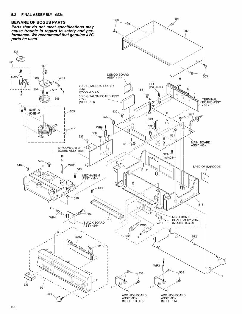
5-2
5.2 FINAL ASSEMBLY <M2>
BEWARE OF BOGUS PARTSParts that do not meet specifications maycause trouble in regard to safety and per-formance. We recommend that genuine JVCparts be used.
525
P516515
516
511
SPEC OF BARCODE
531517
502
504503
503
531
531
ET1(Incl <03>)
530
512
B
J
WR2
E
WR3
D
F
F
MAIN BOARDASSY <03>
TERMINALBOARD ASSY<06>
A
H
H
E
B
MECHANISMASSY <M4>
522
522
OT1(Incl<03>)
524
514
513
A
508
509
507507
506
WR1
510
510
505505F505E
S JACK BOARDASSY <36>
WR4534
G
501A
501B
529
501
D
533
ADV. JOG BOARDASSY <38>(MODEL: B,C,D)
C
3D DIGITAL/2M BOARD ASSY <05>(MODEL: D)
2D DIGITAL BOARD ASSY <05>(MODEL: A,B,C)
DEMOD BOARDASSY <14>
P
521
520
520A
519
GJ
F
533
ADV. JOG BOARDASSY <38>(MODEL: A)
532 C
EWR3
WR5
WR6
538537
S/P CONVERTERBOARD ASSY <87>
MINI FRONTBOARD ASSY <28>(MODEL: B,C,D)
535

5-3
- - - - - - - - - - - - - - - - - - - - - - - - - - - - - - - - - - - - - - - - - - - - - - - - - - - - - - - - - - - - - - - - - - - - - - - - - - - - - - - - - - - - - - - - - - - - - - - - - - - - - - - - - - - - - - - - - - - - - - - - - - - - - - - - - - - - - - - - - - - - - - - - - - - - - - - - - - - - - - - - - - - - - - - - - - - - - - - - - - - - - - - -# REF No. PART No. PART NAME, DESCRIPTION # REF No. PART No. PART NAME, DESCRIPTION
******************************FINAL ASSEMBLY <M2>
! 501 LP10333-027D FRONT PANEL ASSY,A! LP10333-032D FRONT PANEL ASSY,B! LP10333-035D FRONT PANEL ASSY,C! LP10333-037D FRONT PANEL ASSY,D
501A LP20961-007C CASSETTE DOOR,A,B,CLP20961-010C CASSETTE DOOR,D
501B PQ46448 TORSION SPRING! 502 LP10013-051A TOP COVER
503 QYTDSF3010R SCREW,X4 TOP COVER(SIDE)504 QYTDSF3010M SCREW,TOP COVER(REAR)505 LP20981-011A DRUM SUB ASSY,A
LP20981-013A DRUM SUB ASSY,B,C,D505E LP40323-001A CONTACT505F LP30004-014A COMPRESSION SPRING506 PDZ0179-1-4 ROTOR ASSY507 QYSPSP3006Z SCREW,X2
! 508 QAR0169-002 STATOR ASSY509 QYSPSPH2606Z SCREW,X2510 QYTDST2610Z SCREW,X3 DRUM
! 511 LP10108-016E BOTTOM CHASSIS! 512 LP10014-002B BOTTOM COVER
513 LP30312-001B BRACKET(CHASSIS)514 QYTDSF3010Z SCREW,X2515 LP40700-001A SPECIAL SCREW,MECHA516 QYTDSF3010Z SCREW,X2 MECHA
! 517 QMP4A10-170 POWER CORD519 LP40407-001A KNOB ASSY520 LP40370-001E ROLLER ARM ASSY520A PDM4311A-1 ROLLER ASS521 PQ45160 INERTIA PLATE522 LP40226-001A PC SUPPORT,X2524 LP40253-001B STOPPER525 PQ40413 SPECIAL SCREW,MECHA529 LP31019-001C KNOB ASSY,FRONT530 QYTDSF3010Z SCREW,MAIN531 DPSF3010Z SCREW,X3 MAIN532 LP40628-001B PC SUPPORT,MINI FRONT,B,C,D533 QYTPSFG2608Z SCREW,X2 ADV.JOG534 QYTDSF2608Z SCREW,X2 S JACK535 LP30809-001C CAP(JACK)537 QYTDSF3008Z SCREW,S/P CONVERTER538 QYTDSF3008Z SCREW,S/P CONVERTERWR1 QUQ212-0524CG FFC WIRE,DRUM CN3001WR2 WJT0005-001A E-CARD WIRE,A/C HEAD CN2001WR3 QUQ112-0914CG FFC WIRE,ADV.JOG CN7001,A
QUQ112-0914CG FFC WIRE,ADV.JOG CN7005,B,C,DWR4 QUQ212-0456CG FFC WIRE,S JACK CN916WR5 QUQ112-0914CG FFC WIRE,MINI FRONT CN7001,B,C,DWR6 QUQ112-1140CG FFC WIRE,S/P CONVERTER CN511

5-4
5.3 MECHANISM ASSEMBLY <M4>
Classifi-Part No.
Symbol incation drawing
Grease KYODO-SH-P AA
Oil COSMO-HV56 BB
NOTE:The section marked in AA and BBindicate lubrication and greasing areas.
AA
46
143
A/C HEADBOARD ASSY <12>
LOADING MOTORBOARD ASSY <55>
124
128
131
122
141139
130 137
143
138
139
140
129
127
4443
42
123AA
AA
AA
AA
AA
BB
AA
AA
AA
AA
AA
AA
AA
AA
AAAA
AA
AA
BB
AA
AA
AA
AA
BB
105
120
75
74
121
72
13276
73
142
88
10489
135134
78
107
101
40
106
4957
5459
61
62
85
91
1
111
6083
82
52
58
5539
53
51
1
112
113
151
116115
117
118
114
119
66
63
6867
65
6470
2325
2418
19 20
16 27
71
87
22
9996
100
31
8081
34
37
35103
32102
36
38
108
109
90
92
AA
AA
69
110
15
84
86
13
12107
2613
215
6
411
3
10
7
94
93
97
95

5-5
- - - - - - - - - - - - - - - - - - - - - - - - - - - - - - - - - - - - - - - - - - - - - - - - - - - - - - - - - - - - - - - - - - - - - - - - - - - - - - - - - - - - - - - - - - - - - - - - - - - - - - - - - - - - - - - - - - - - - - - - - - - - - - - - - - - - - - - - - - - - - - - - - - - - - - - - - - - - - - - - - - - - - - - - - - - - - - - - - - - - - - - -# REF No. PART No. PART NAME, DESCRIPTION # REF No. PART No. PART NAME, DESCRIPTION
******************************MECHANISM ASSEMBLY <M4>
1 LP20821-009A MAIN DECK ASSY3 LP30492-002B GUIDE POLE GUARD4 NAH0001-001 FULL ERASE HEAD5 LP40701-001A GUIDE POLE(SUPPLY)6 QYTDST2608Z SCREW,FE HEAD7 LP40637-002A TENSION STUD BASE ASSY10 QYTDST2606Z SCREW11 LP30409-002C UV CATCHER 2 (SUPPLY)12 LP30409-002C UV CATCHER 2 (TAKE UP)13 QYTPST2606Z SCREW,X215 LP30223-003C LOADING ARM GEAR SHAFT16 QYTDST2606Z SCREW18 LP30224-001B LOADING ARM GEAR(SUPPLY)19 LP40099-001A TORSION ARM20 LP40100-001A PIN21 LP40101-006A POLE BASE ASSY(SUPPLY)22 QYSPSTG2606Z SCREW23 LP40103-002B LOADING ARM GEAR(TAKE UP)24 LP40099-001A TORSION ARM25 LP40100-002A PIN26 LP40104-006A POLE BASE ASSY(TAKE UP)27 QYSPSTG2606Z SCREW31 LP20233-004B ROTARY ENCODER GUIDE32 QYTPST2606Z SCREW34 LP30226-004E CONTROL PLATE GUIDE35 QYTPST2605Z SCREW36 LP30249-003B TAKE UP LEVER37 LP30003-006A TENSION SPRING38 LP40119-002A TAKE UP HEAD39 LP20234-004B LID GUIDE40 QYTDST2606Z SCREW,X242 LP40105-003A PINCH ROLLER ARM ASSY43 LP40753-001A PINCH ROLLER SHEET344 LP40148-002A TORSION SPRING46 LP40149-001C PRESS LEVER ASSY49 LP40106-007A GUIDE ARM ASSY51 LP40134-002A TENSION SPRING52 QAH0058-001 AC HEAD53 LP30228-001C HEAD BASE54 LP30004-013A COMPRESSION SPRING,X355 LP40236-001A COMPRESSION SPRING57 LP40213-002B SPECIAL SCREW,X358 QYTDST2608Z SCREW,X259 QAR0023-001 LOADING MOTOR60 PQ43546-1-2 MOTOR PULLEY61 LP30230-003D MOTOR GUIDE62 QYTPSP3003Z SCREW,X263 LP30005-003A BELT,LOADING MOTOR64 LP20791-002D CONTROL CAM65 PQM30017-24 SLIT WASHER66 LP40120-001A WORM GEAR67 LP40107-002A LINK LEVER ASSY68 PQM30017-24 SLIT WASHER69 LP10201-003G CONTROL PLATE70 LP40379-001B CONTROL BRACKET(1)71 QYTDSF2608M SCREW72 LP40108-002A TENSION ARM ASSY73 LP30003-010A TENSION SPRING74 LP40109-003D TENSION BRAKE ASSY75 PQ46302-1-3 ADJUST PIN
76 LP30232-002A TENSION ARM BEARING78 LP40532-008B MAIN BRAKE ASSY (SUPPLY)80 LP40111-011A MAIN BRAKE ASSY (TAKE UP)81 LP30003-026A TENSION SPRING82 LP40112-001F SUB BRAKE ASSY(TAKE UP)83 LP40357-002A TENSION SPRING84 LP40461-001A CAPSTAN BRAKE ASSY85 QAR0087-005 CAPSTAN MOTOR86 QYTDSF2606M SCREW,X387 LP30005-007A BELT,CAPSTAN MOTOR88 LP40114-012A IDLER ARM ASSY89 LP30016-001A SLIT WASHER90 LP40593-001A CLUTCH UNIT 391 LP30002-097A SPACER,CAPSTAN MOTOR92 PQM30017-47 SLIT WASHER93 LP30696-002A CLUTCH GEAR 494 LP30697-003A COUPLING GEAR95 LP40554-002A COMPRESSION SPRING96 LP40442-001A DIRECT GEAR97 LP30017-019A SPACER,C.GEAR499 LP40483-002A COMPRESSION SPRING100 LP30016-001A SLIT WASHER,DIRECT GEAR101 LP30016-001A SLIT WASHER,REEL DISK(SUPPLY)102 LP40484-001J CHANGE LEVER ASSY103 LP40512-002B COMPRESSION SPRING104 LP30236-002C IDLER LEVER105 LP20237-004A REEL DISK (SUPPLY)106 LP20238-004A REEL DISK (TAKE UP)107 LP30017-022A SPACER,X2108 QSW0554-003 ROTARY ENCODER109 QYTPST2620Z SCREW110 LP30237-002B CASSETTE GEAR111 LP30239-002G LIMIT GEAR(1)112 LP30240-002G LIMIT GEAR(2)113 LP40136-001E TORSION SPRING114 LP30242-002A RELAY GEAR115 LP30339-002E OPENER GUIDE116 LP40545-001A TORSION SPRING117 LP40214-001B C.H.BRACKET118 PQM30017-47 SLIT WASHER,X2119 LP30243-002A DRIVE GEAR120 LP20240-001G DRIVE ARM121 LP40137-001A TORSION SPRING122 LP10081-002P SIDE HOLDER(L)123 LP10082-002U SIDE HOLDER(R)124 LP30255-006B LOCK LEVER(L)127 LP30256-001H LOCK LEVER(R)128 LP40168-003A TORSION SPRING(L)129 LP40218-001B TORSION SPRING(R)130 LP30257-001G CASSETTE HOLDER131 PQ40919-30 SPACER,EARTH PLATE132 LP30244-002G GUIDE RAIL134 LP30245-002F REC SAFETY LEVER135 LP30003-004A TENSION SPRING137 LP20578-001C TOP GUIDE138 LP30500-001C HOLD PLATE139 LP40450-003A PAD,X2140 LP30003-025B TENSION SPRING141 LP30003-024A TENSION SPRING142 LP40481-003A ROLLER CAM ASSY143 LP30019-014A PAD,X2152 LP20324-003B DOOR OPENER

- - - - - - - - - - - - - - - - - - - - - - - - - - - - - - - - - - - - - - - - - - - - - - - - - - - - - - - - - - - - - - - - - - - - - - - - - - - - - - - - - - - - - - - - - - - - - - - - - - - - - - - - - - - - - - - - - - - - - - - - - - - - - - - - - - - - - - - - - - - - - - - - - - - - - - - - - - - - - - - - - - - - - - - - - - - - - - - - - - - - - - - -# REF No. PART No. PART NAME, DESCRIPTION # REF No. PART No. PART NAME, DESCRIPTION
5-6
5.4 ELECTRICAL PARTS LIST MODEL MARK MODEL MARK
HR-S6850MS A HR-S7851MS C HR-S7850MS B HR-S8850MS D
******************************MAIN BOARD ASSEMBLY <03>
PW1 LPA10140-03B MAIN BOARD ASSY,B,CLPA10140-06A MAIN BOARD ASSY,DLPA10140-09A MAIN BOARD ASSY,A
IC1 JCP8050-MSA ICIC2 MM1113XF ICIC201 LC74775-9750 ICIC301 LA7358 ICIC3001 HD6432194SAD12F IC(MCU)IC3002 IC-PST3427U-X ICIC3003 24LC32A-I/SN-X IC
or HN58X2432FPI ICor BR24C32F IC
IC3004 BA6956AN ICIC5301 L5431 IC
or MM1431AT ICor UTCTL431 IC
IC7001 PT6312LQ ICor UPD16312GB/H/ IC
IC7003 GP1U291Q IR DETECT UNITor PIC-28143LJ IR DETECT UNITor PNA4652M00YC IR DETECT UNITor PIC-37143LJ IR DETECT UNIT
Q1 2SC4081/S/-X TRANSISTOR,AQ2 2SC4081/S/-X TRANSISTOR,AQ3 2SC4081/S/-X TRANSISTOR,AQ4 2SC4081/S/-X TRANSISTOR,AQ5 2SB1218A/QR/-X TRANSISTOR
or 2PA1576/R/-X TRANSISTORor 2SA1576A/QR/-X TRANSISTOR
Q7 2SD1819A/QRS/-X TRANSISTORor 2PC4081/R/-X TRANSISTORor 2SC4081/QRS/-X TRANSISTOR
Q8 2SD1819A/QRS/-X TRANSISTORor 2SC4081/QRS/-X TRANSISTORor 2PC4081/R/-X TRANSISTOR
Q9 2SB1218A/QR/-X TRANSISTORor 2PA1576/R/-X TRANSISTORor 2SA1576A/QR/-X TRANSISTOR
Q10 2SA1576A/QR/-X TRANSISTORQ11 DTC144WU TRANSISTOR,A,B,C
or PDTC144WU TRANSISTOR,A,B,Cor RN1309 TRANSISTOR,A,B,Cor UN521E TRANSISTOR,A,B,C
Q14 DTA144WU TRANSISTORor PDTA144WU TRANSISTORor RN2309 TRANSISTORor UN511E TRANSISTOR
Q17 DTC144WU TRANSISTORor PDTC144WU TRANSISTORor RN1309 TRANSISTORor UN521E TRANSISTOR
Q21 2SB1218A/QR/-X TRANSISTORor 2SA1576A/QR/-X TRANSISTORor 2PA1576/R/-X TRANSISTOR
Q24 2SB1218A/QR/-X TRANSISTORor 2PA1576/R/-X TRANSISTORor 2SA1576A/QR/-X TRANSISTOR
Q25 DTC144WU TRANSISTOR,Dor PDTC144WU TRANSISTOR,Dor RN1309 TRANSISTOR,Dor UN521E TRANSISTOR,D
Q38 2SD1819A/QRS/-X TRANSISTORor 2SC4081/QRS/-X TRANSISTORor 2PC4081/R/-X TRANSISTOR
Q40 DTC144WU TRANSISTOR,A,B,Cor PDTC144WU TRANSISTOR,A,B,Cor RN1309 TRANSISTOR,A,B,Cor UN521E TRANSISTOR,A,B,C
Q41 DTC144WU TRANSISTORor PDTC144WU TRANSISTORor RN1309 TRANSISTORor UN521E TRANSISTOR
Q207 2SB1218A/QR/-X TRANSISTORor 2PA1576/R/-X TRANSISTORor 2SA1576A/QR/-X TRANSISTOR
Q208 2SD1819A/QRS/-X TRANSISTORor 2SC4081/QRS/-X TRANSISTORor 2PC4081/R/-X TRANSISTOR
Q301 2SB1218A/QR/-X TRANSISTORor 2PA1576/R/-X TRANSISTORor 2SA1576A/QR/-X TRANSISTOR
Q302 UN511E TRANSISTORor DTA144WU TRANSISTORor PDTA144WU TRANSISTORor RN2309 TRANSISTOR
Q401 2SA1576A/QR/-X TRANSISTOR,B,C,DQ402 2SA1576A/QR/-X TRANSISTOR,B,C,DQ403 DTC144WU TRANSISTOR,B,C,D
or PDTC144WU TRANSISTOR,B,C,Dor RN1309 TRANSISTOR,B,C,Dor UN521E TRANSISTOR,B,C,D
Q404 DTC144WU TRANSISTOR,B,C,Dor PDTC144WU TRANSISTOR,B,C,Dor RN1309 TRANSISTOR,B,C,Dor UN521E TRANSISTOR,B,C,D
Q405 2SA1576A/QR/-X TRANSISTOR,B,C,DQ2001 2SC4081/QRS/-X TRANSISTOR
or 2SD1819A/QRS/-X TRANSISTORor 2PC4081/R/-X TRANSISTOR
Q2002 2SC4081/QRS/-X TRANSISTORor 2PC4081/R/-X TRANSISTORor 2SD1819A/QRS/-X TRANSISTOR
Q2003 DTA144WU TRANSISTORor PDTA144WU TRANSISTORor RN2309 TRANSISTORor UN511E TRANSISTOR
Q2004 DTC114EU TRANSISTORor PDTC114EU TRANSISTORor RN1302 TRANSISTORor UN5211 TRANSISTOR
Q2051 2SC4081/QRS/-X TRANSISTORor 2PC4081/R/-X TRANSISTORor 2SD1819A/QRS/-X TRANSISTOR
Q2052 2SA1576A/QR/-X TRANSISTORor 2SB1218A/QR/-X TRANSISTORor 2PA1576/R/-X TRANSISTOR
Q2053 DTC144WU TRANSISTORor PDTC144WU TRANSISTOR

5-7
- - - - - - - - - - - - - - - - - - - - - - - - - - - - - - - - - - - - - - - - - - - - - - - - - - - - - - - - - - - - - - - - - - - - - - - - - - - - - - - - - - - - - - - - - - - - - - - - - - - - - - - - - - - - - - - - - - - - - - - - - - - - - - - - - - - - - - - - - - - - - - - - - - - - - - - - - - - - - - - - - - - - - - - - - - - - - - - - - - - - - - - -# REF No. PART No. PART NAME, DESCRIPTION # REF No. PART No. PART NAME, DESCRIPTION
or RN1309 TRANSISTORor UN521E TRANSISTOR
Q2054 2SA1576A/QR/-X TRANSISTORor 2PA1576/R/-X TRANSISTORor 2SB1218A/QR/-X TRANSISTOR
Q2055 DTC144WU TRANSISTORor PDTC144WU TRANSISTORor UN521E TRANSISTORor RN1309 TRANSISTOR
Q2061 2SC4081/QRS/-X TRANSISTOR,B,C,Dor 2PC4081/R/-X TRANSISTOR,B,C,Dor 2SD1819A/QRS/-X TRANSISTOR,B,C,D
Q2062 2SA1576A/QR/-X TRANSISTOR,B,C,Dor 2PA1576/R/-X TRANSISTOR,B,C,Dor 2SB1218A/QR/-X TRANSISTOR,B,C,D
Q2063 DTC144WU TRANSISTOR,B,C,Dor PDTC144WU TRANSISTOR,B,C,Dor RN1309 TRANSISTOR,B,C,Dor UN521E TRANSISTOR,B,C,D
Q2251 DTA144WU TRANSISTORor PDTA144WU TRANSISTORor RN2309 TRANSISTORor UN511E TRANSISTOR
Q2252 DTC114EU TRANSISTORor PDTC114EU TRANSISTORor RN1302 TRANSISTORor UN5211 TRANSISTOR
Q3001 2SD1819A/QRS/-X TRANSISTORor 2PC4081/R/-X TRANSISTORor 2SC4081/QRS/-X TRANSISTOR
Q3002 PTZ-NV16 PHOTO TRANSISTORor PTZ-NV16A PHOTO TRANSISTOR
Q3003 PTZ-NV16 PHOTO TRANSISTORor PTZ-NV16A PHOTO TRANSISTOR
Q3004 2SD1819A/QRS/-X TRANSISTORor 2SC4081/QRS/-X TRANSISTORor 2PC4081/R/-X TRANSISTOR
Q3005 2SD1819A/QRS/-X TRANSISTORor 2SC4081/QRS/-X TRANSISTORor 2PC4081/R/-X TRANSISTOR
Q3007 UN521E TRANSISTORor PDTC144WU TRANSISTORor DTC144WU TRANSISTORor RN1309 TRANSISTOR
Q4001 UN5211 TRANSISTORor RN1302 TRANSISTORor DTC114EU TRANSISTORor PDTC114EU TRANSISTOR
Q5101 2SK2632-CB14 POWER MOS FETor 2SK2632 POWER MOS FETor 2SK2129-LT POWER MOS FETor 2SK2129 POWER MOS FET
Q5102 2SD2144S/UV/-T TRANSISTORQ5301 2SB1256 TRANSISTORQ5302 2SD2375/QP/ TRANSISTORQ5303 2SD1819A/RS/-X TRANSISTOR
or 2PC4081/R/-X TRANSISTORor 2SC4081/RS/-X TRANSISTOR
Q5304 2SC3616/ML/-T TRANSISTORQ5305 DTA114EU TRANSISTOR
or PDTA114EU TRANSISTOR
or UN5111 TRANSISTORor RN2302 TRANSISTOR
Q5306 DTC114EU TRANSISTORor PDTC114EU TRANSISTORor UN5211 TRANSISTORor RN1302 TRANSISTOR
Q5308 2SA1576A/RS/-X TRANSISTORQ5311 DTC114TU TRANSISTOR
or PDTC114TU TRANSISTORor RN1311 TRANSISTORor UN5215 TRANSISTOR
Q5312 2SD2144S/UV/-T TRANSISTORQ5318 DTA114EU TRANSISTOR
or RN2302 TRANSISTORor UN5111 TRANSISTORor PDTA114EU TRANSISTOR
Q5320 DTC114EU TRANSISTORor PDTC114EU TRANSISTORor RN1302 TRANSISTORor UN5211 TRANSISTOR
Q5322 DTC114TU TRANSISTORor PDTC114TU TRANSISTORor RN1311 TRANSISTORor UN5215 TRANSISTOR
Q5323 2SB927/ST/-T TRANSISTORQ6030 2SB1218A/QR/-X TRANSISTOR
or 2SA1576A/QR/-X TRANSISTORor 2PA1576/R/-X TRANSISTOR
Q6031 DTC114EU TRANSISTORor PDTC114EU TRANSISTORor RN1302 TRANSISTORor UN5211 TRANSISTOR
Q6032 DTC114EU TRANSISTORor PDTC114EU TRANSISTORor RN1302 TRANSISTORor UN5211 TRANSISTOR
Q7201 2SC1317/RS/-T TRANSISTORD1 DA204U DIODED6 MTZJ5.1C ZENER DIODED201 QRE141J-152Y RESISTOR 1.5kØ,1/4WD202 QRE141J-101Y RESISTOR 100Ø,1/4WD203 QRE141J-101Y RESISTOR 100Ø,1/4WD2202 MTZJ8.2C ZENER DIODED3001 LNB2301L01VI LE DIODED3002 1SS133 DIODE
or 1SS270A DIODED3003 RD39ES/B3/-T2 ZENER DIODE
or MTZJ39C ZENER DIODED3004 11ES2 DIODE
or 1A3G DIODED3005 11ES2 DIODE
or 1A3G DIODED3008 1SS355 DIODED4001 QUY153-050Y IM BUS WIRED4002 QUY153-050Y IM BUS WIRED5001 S1WB/A/60-4102 BRIDGE DIODE
or S1WB/A/60-X BRIDGE DIODEor S1WB(A)60F4072X BRIDGE DIODE
D5101 AU01 FR DIODEor ERA18-04-T2 FR DIODEor 1SR153-400-T2 FR DIODE

- - - - - - - - - - - - - - - - - - - - - - - - - - - - - - - - - - - - - - - - - - - - - - - - - - - - - - - - - - - - - - - - - - - - - - - - - - - - - - - - - - - - - - - - - - - - - - - - - - - - - - - - - - - - - - - - - - - - - - - - - - - - - - - - - - - - - - - - - - - - - - - - - - - - - - - - - - - - - - - - - - - - - - - - - - - - - - - - - - - - - - - -# REF No. PART No. PART NAME, DESCRIPTION # REF No. PART No. PART NAME, DESCRIPTION
5-8
or 10ELS4 FR DIODED5102 AU01 FR DIODE
or ERA18-04-T2 FR DIODEor 10ELS4 FR DIODEor 1SR153-400-T2 FR DIODE
D5103 1SS133 DIODEor 1SS270A DIODE
D5105 1SS133 DIODEor 1SS270A DIODE
D5201 AK04 DIODE,B,C,DAU01Z FR DIODE,A
or 1S4 SB DIODE,B,C,Dor 11EQS04 SB DIODE,B,C,Dor 10ELS2 FR DIODE,A
D5203 AU01Z FR DIODEor 10ELS2 FR DIODE
D5204 AU01Z FR DIODEor 10ELS2 FR DIODE
D5206 FMB-24 BARRIER DIODEor SB640FCT SB DIODEor SF5SC4 SB DIODEor YG801C04 SB DIODEor FSQ05A04B SB DIODE
D5209 ERA18-02-T2 FR DIODEor 1SR153-400-T2 FR DIODEor 10ELS2 FR DIODEor PG104RS FR DIODE
D5210 AU01Z FR DIODEor ERA18-02-T2 FR DIODEor 10ELS2 FR DIODEor PG104RS FR DIODEor 1SR153-400-T2 FR DIODE
D5211 AU01Z FR DIODEor ERA18-02-T2 FR DIODEor 1SR153-400-T2 FR DIODEor 10ELS2 FR DIODEor PG104RS FR DIODE
D5301 MTZJ15C ZENER DIODEor RD15ES/B3/-T2 ZENER DIODE
D5302 1SS133 DIODEor 1SS270A DIODE
D5303 RD5.1JS/B2/-T2 ZENER DIODEor MA4051N/M/-T2 ZENER DIODE
D5304 1SS133 DIODEor 1SS270A DIODE
D5305 AK04 DIODEor 11EQS04 SB DIODEor 1S4 SB DIODE
D5307 11ES2 DIODEor 1A3G DIODEor ERA15-02-T2 DIODE
D5308 MTZJ11B ZENER DIODEor RD11ES/B2/-T2 ZENER DIODE
D5309 MTZJ27C ZENER DIODEor RD27ES/B3/-T2 ZENER DIODE
D5310 1SS133 DIODEor 1SS270A DIODE
D5316 QUY160-100Y IM BUS WIRED5317 1SS133 DIODE
or 1SS270A DIODED5318 11ES2 DIODE
or 1A3G DIODEor ERA15-02-T2 DIODE
D5319 11ES2 DIODEor 1A3G DIODEor ERA15-02-T2 DIODE
D6002 HZ30-2L-T2 ZENER DIODEor HZ30-2LTD Z DIODE (M)
D7001 RD9.1ES/B2/-T2 ZENER DIODEor UZ9.1BSB ZENER DIODEor MTZJ9.1B ZENER DIODE
D7003 1SS133 DIODEor 1SS270A DIODE
D7004 1SS133 DIODEor 1SS270A DIODE
D7005 1SS133 DIODEor 1SS270A DIODE
D7006 1SS133 DIODE,B,C,Dor 1SS270A DIODE,B,C,D
D7008 SLR-325MC-T LE DIODED7009 SLR-325VC-T LE DIODER1 NRVA02D-682X CMF RESISTOR 6.8kØ,1/10WR2 NRVA02D-152X CMF RESISTOR 1.5kØ,1/10WR3 NRSA02J-182X MG RESISTOR 1.8kØ,1/10WR4 NRSA02J-0R0X MG RESISTOR 0Ø,1/10WR5 NRSA02J-0R0X MG RESISTOR 0Ø,1/10WR6 NRSA02J-273X MG RESISTOR 27kØ,1/10WR7 NRSA02J-681X MG RESISTOR 680Ø,1/10WR8 NRSA02J-0R0X MG RESISTOR 0Ø,1/10WR9 NRSA02J-0R0X MG RESISTOR 0Ø,1/10WR21 NRSA02J-0R0X MG RESISTOR,A 0Ø,1/10WR22 NRSA02J-0R0X MG RESISTOR,A 0Ø,1/10WR23 NRSA02J-182X MG RESISTOR 1.8kØ,1/10WR25 NRSA02J-103X MG RESISTOR 10kØ,1/10WR26 NRSA02J-682X MG RESISTOR 6.8kØ,1/10WR27 NRSA02J-221X MG RESISTOR 220Ø,1/10WR28 NRSA02J-221X MG RESISTOR 220Ø,1/10WR29 NRSA02J-561X MG RESISTOR 560Ø,1/10WR30 NRSA02J-0R0X MG RESISTOR 0Ø,1/10WR31 NRSA02J-152X MG RESISTOR 1.5kØ,1/10WR32 NRSA02J-471X MG RESISTOR 470Ø,1/10WR33 NRSA02J-153X MG RESISTOR 15kØ,1/10WR36 NRSA02J-182X MG RESISTOR 1.8kØ,1/10WR38 NRSA02J-102X MG RESISTOR 1kØ,1/10WR39 NRSA02J-103X MG RESISTOR,A,B,C 10kØ,1/10WR40 NRSA02J-222X MG RESISTOR 2.2kØ,1/10WR41 NRSA02J-392X MG RESISTOR 3.9kØ,1/10WR42 NRSA02J-681X MG RESISTOR 680Ø,1/10WR46 NRSA02J-561X MG RESISTOR,A,B,C 560Ø,1/10W
NRSA02J-221X MG RESISTOR,D 220Ø,1/10WR48 QRE141J-102Y RESISTOR 1kØ,1/4WR51 NRSA02J-122X MG RESISTOR 1.2kØ,1/10WR65 NRSA02J-102X MG RESISTOR 1kØ,1/10WR68 NRSA02J-102X MG RESISTOR 1kØ,1/10WR70 NRSA02J-0R0X MG RESISTOR 0Ø,1/10WR77 NRSA02J-103X MG RESISTOR,A,B,C 10kØ,1/10W
NRSA02J-223X MG RESISTOR,D 22kØ,1/10WR88 NRSA02J-0R0X MG RESISTOR 0Ø,1/10WR90 NRSA02J-391X MG RESISTOR 390Ø,1/10WR92 NRSA02J-152X MG RESISTOR 1.5kØ,1/10WR93 NRSA02J-222X MG RESISTOR 2.2kØ,1/10WR104 NRSA02J-682X MG RESISTOR 6.8kØ,1/10W

5-9
- - - - - - - - - - - - - - - - - - - - - - - - - - - - - - - - - - - - - - - - - - - - - - - - - - - - - - - - - - - - - - - - - - - - - - - - - - - - - - - - - - - - - - - - - - - - - - - - - - - - - - - - - - - - - - - - - - - - - - - - - - - - - - - - - - - - - - - - - - - - - - - - - - - - - - - - - - - - - - - - - - - - - - - - - - - - - - - - - - - - - - - -# REF No. PART No. PART NAME, DESCRIPTION # REF No. PART No. PART NAME, DESCRIPTION
R113 NRSA02J-101X MG RESISTOR 100Ø,1/10WR117 NRSA02J-104X MG RESISTOR,D 100kØ,1/10WR118 NRSA02J-0R0X MG RESISTOR 0Ø,1/10WR201 NRSA02J-0R0X MG RESISTOR 0Ø,1/10WR202 NRSA02J-103X MG RESISTOR 10kØ,1/10WR208 NRSA02J-222X MG RESISTOR 2.2kØ,1/10WR209 NRSA02J-512X MG RESISTOR 5.1kØ,1/10WR210 NRSA02J-182X MG RESISTOR 1.8kØ,1/10WR211 NRSA02J-562X MG RESISTOR 5.6kØ,1/10WR212 NRSA02J-101X MG RESISTOR 100Ø,1/10WR213 QRE141J-0R0Y RESISTOR 0Ø,1/4WR216 NRSA02J-103X MG RESISTOR 10kØ,1/10WR224 NRSA02J-101X MG RESISTOR 100Ø,1/10WR225 NRSA02J-471X MG RESISTOR 470Ø,1/10WR226 NRSA02J-102X MG RESISTOR 1kØ,1/10WR301 NRSA02J-273X MG RESISTOR 27kØ,1/10WR302 NRSA02J-124X MG RESISTOR 120kØ,1/10WR303 NRSA02J-273X MG RESISTOR 27kØ,1/10WR304 NRSA02J-682X MG RESISTOR 6.8kØ,1/10WR305 NRSA02J-473X MG RESISTOR 47kØ,1/10WR306 NRSA02J-273X MG RESISTOR 27kØ,1/10WR307 NRSA02J-222X MG RESISTOR 2.2kØ,1/10WR308 NRSA02J-222X MG RESISTOR 2.2kØ,1/10WR309 NRSA02J-0R0X MG RESISTOR 0Ø,1/10WR310 NRSA02J-223X MG RESISTOR 22kØ,1/10WR311 NRSA02J-472X MG RESISTOR 4.7kØ,1/10WR312 NRSA02J-272X MG RESISTOR 2.7kØ,1/10WR313 NRSA02J-223X MG RESISTOR 22kØ,1/10WR314 NRVA02D-243X CMF RESISTOR 24kØ,1/10WR315 NRSA02J-564X MG RESISTOR 560kØ,1/10WR316 NRSA02J-124X MG RESISTOR 120kØ,1/10WR318 NRSA02J-821X MG RESISTOR 820Ø,1/10WR329 NRSA02J-0R0X MG RESISTOR 0Ø,1/10WR401 NRSA02J-221X MG RESISTOR,B,C,D 220Ø,1/10WR402 NRSA02J-681X MG RESISTOR,B,C,D 680Ø,1/10WR403 NRSA02J-561X MG RESISTOR,B,C,D 560Ø,1/10WR404 NRSA02J-473X MG RESISTOR,B,C,D 47kØ,1/10WR405 NRSA02J-683X MG RESISTOR,B,C,D 68kØ,1/10WR406 NRSA02J-393X MG RESISTOR,B,C,D 39kØ,1/10WR407 NRSA02J-472X MG RESISTOR,B,C,D 4.7kØ,1/10WR408 NRSA02J-473X MG RESISTOR,B,C,D 47kØ,1/10WR2003 NRSA02J-101X MG RESISTOR 100Ø,1/10WR2005 NRSA02J-0R0X MG RESISTOR 0Ø,1/10WR2006 NRSA02J-393X MG RESISTOR 39kØ,1/10WR2007 NRSA02J-393X MG RESISTOR 39kØ,1/10WR2008 NRSA02J-123X MG RESISTOR 12kØ,1/10WR2009 NRSA02J-123X MG RESISTOR 12kØ,1/10WR2010 NRSA02J-123X MG RESISTOR 12kØ,1/10WR2013 NRSA02J-682X MG RESISTOR 6.8kØ,1/10WR2014 NRSA02J-224X MG RESISTOR 220kØ,1/10WR2015 NRSA02J-181X MG RESISTOR 180Ø,1/10WR2016 NRSA02J-393X MG RESISTOR 39kØ,1/10WR2017 NRSA02J-183X MG RESISTOR 18kØ,1/10WR2018 NRSA02J-472X MG RESISTOR 4.7kØ,1/10WR2019 NRSA02J-472X MG RESISTOR 4.7kØ,1/10WR2053 NRSA02J-472X MG RESISTOR 4.7kØ,1/10WR2054 NRSA02J-123X MG RESISTOR,A 12kØ,1/10W
NRSA02J-153X MG RESISTOR,B,C,D 15kØ,1/10WR2055 NRSA02J-3R3X MG RESISTOR 3.3Ø,1/10WR2056 NRSA02J-820X MG RESISTOR,A 82Ø,1/10W
NRSA02J-101X MG RESISTOR,B,C,D 100Ø,1/10W
R2057 NRSA02J-473X MG RESISTOR 47kØ,1/10WR2058 NRSA02J-183X MG RESISTOR 18kØ,1/10WR2059 NRSA02J-473X MG RESISTOR 47kØ,1/10WR2060 NRSA02J-183X MG RESISTOR 18kØ,1/10WR2061 NRSA02J-273X MG RESISTOR,B,C,D 27kØ,1/10WR2062 NRSA02J-3R3X MG RESISTOR,B,C,D 3.3Ø,1/10WR2063 NRSA02J-151X MG RESISTOR,B,C,D 150Ø,1/10WR2064 NRSA02J-473X MG RESISTOR,B,C,D 47kØ,1/10WR2065 NRSA02J-183X MG RESISTOR,B,C,D 18kØ,1/10WR2201 QRE141J-121Y RESISTOR 120Ø,1/4WR2202 NRSA02J-222X MG RESISTOR 2.2kØ,1/10WR2203 NRSA02J-222X MG RESISTOR 2.2kØ,1/10WR2204 NRSA02J-102X MG RESISTOR 1kØ,1/10WR2205 NRSA02J-102X MG RESISTOR 1kØ,1/10WR2206 NRSA02J-101X MG RESISTOR 100Ø,1/10WR2208 NRSA02J-101X MG RESISTOR 100Ø,1/10WR2209 NRSA02J-101X MG RESISTOR 100Ø,1/10WR2210 NRSA02J-103X MG RESISTOR 10kØ,1/10WR2211 NRSA02J-103X MG RESISTOR 10kØ,1/10WR2213 NRSA02J-393X MG RESISTOR 39kØ,1/10WR2215 NRSA02J-153X MG RESISTOR 15kØ,1/10WR2217 NRSA02J-0R0X MG RESISTOR 0Ø,1/10WR2218 NRSA02J-393X MG RESISTOR 39kØ,1/10WR2219 NRSA02J-393X MG RESISTOR 39kØ,1/10WR2220 NRSA02J-393X MG RESISTOR 39kØ,1/10WR2222 NRSA02J-123X MG RESISTOR 12kØ,1/10WR2223 NRSA02J-123X MG RESISTOR 12kØ,1/10WR2224 NRSA02J-123X MG RESISTOR 12kØ,1/10WR2225 NRSA02J-153X MG RESISTOR 15kØ,1/10WR2226 NRSA02J-123X MG RESISTOR 12kØ,1/10WR2227 NRSA02J-123X MG RESISTOR 12kØ,1/10WR2228 NRSA02J-103X MG RESISTOR 10kØ,1/10WR2229 NRSA02J-563X MG RESISTOR 56kØ,1/10WR2251 NRSA02J-102X MG RESISTOR 1kØ,1/10WR3011 NRSA02J-102X MG RESISTOR 1kØ,1/10WR3012 NRSA02J-102X MG RESISTOR 1kØ,1/10WR3013 NRSA02J-102X MG RESISTOR 1kØ,1/10WR3014 NRSA02J-102X MG RESISTOR 1kØ,1/10WR3015 NRSA02J-102X MG RESISTOR 1kØ,1/10WR3016 NRSA02J-102X MG RESISTOR 1kØ,1/10WR3017 NRSA02J-102X MG RESISTOR 1kØ,1/10WR3018 NRSA02J-682X MG RESISTOR 6.8kØ,1/10WR3019 NRSA02J-102X MG RESISTOR 1kØ,1/10WR3020 NRSA02J-102X MG RESISTOR 1kØ,1/10WR3021 NRSA02J-102X MG RESISTOR 1kØ,1/10WR3022 NRSA02J-102X MG RESISTOR 1kØ,1/10WR3025 NRSA02J-102X MG RESISTOR 1kØ,1/10WR3026 NRSA02J-102X MG RESISTOR 1kØ,1/10WR3027 NRSA02J-102X MG RESISTOR 1kØ,1/10WR3029 NRSA02J-102X MG RESISTOR 1kØ,1/10WR3030 NRSA02J-102X MG RESISTOR 1kØ,1/10WR3031 NRSA02J-102X MG RESISTOR 1kØ,1/10WR3032 NRSA02J-102X MG RESISTOR 1kØ,1/10WR3033 NRSA02J-0R0X MG RESISTOR 0Ø,1/10WR3034 NRSA02J-0R0X MG RESISTOR 0Ø,1/10WR3035 NRSA02J-0R0X MG RESISTOR 0Ø,1/10WR3036 NRSA02J-0R0X MG RESISTOR 0Ø,1/10WR3038 NRSA02J-152X MG RESISTOR 1.5kØ,1/10WR3039 NRSA02J-102X MG RESISTOR 1kØ,1/10WR3040 NRSA02J-472X MG RESISTOR 4.7kØ,1/10WR3041 NRSA02J-0R0X MG RESISTOR 0Ø,1/10W

- - - - - - - - - - - - - - - - - - - - - - - - - - - - - - - - - - - - - - - - - - - - - - - - - - - - - - - - - - - - - - - - - - - - - - - - - - - - - - - - - - - - - - - - - - - - - - - - - - - - - - - - - - - - - - - - - - - - - - - - - - - - - - - - - - - - - - - - - - - - - - - - - - - - - - - - - - - - - - - - - - - - - - - - - - - - - - - - - - - - - - - -# REF No. PART No. PART NAME, DESCRIPTION # REF No. PART No. PART NAME, DESCRIPTION
5-10
R3042 NRSA02J-0R0X MG RESISTOR 0Ø,1/10WR3044 NRSA02J-0R0X MG RESISTOR 0Ø,1/10WR3046 NRSA02J-102X MG RESISTOR 1kØ,1/10WR3047 NRSA02J-102X MG RESISTOR 1kØ,1/10WR3048 NRSA02J-0R0X MG RESISTOR 0Ø,1/10WR3049 NRSA02J-0R0X MG RESISTOR 0Ø,1/10WR3050 NRSA02J-0R0X MG RESISTOR 0Ø,1/10WR3051 NRSA02J-471X MG RESISTOR 470Ø,1/10WR3052 NRSA02J-471X MG RESISTOR 470Ø,1/10WR3053 NRSA02J-471X MG RESISTOR 470Ø,1/10WR3054 NRSA02J-102X MG RESISTOR 1kØ,1/10WR3055 NRSA02J-102X MG RESISTOR 1kØ,1/10WR3056 NRSA02J-102X MG RESISTOR 1kØ,1/10WR3057 NRSA02J-102X MG RESISTOR 1kØ,1/10WR3058 NRSA02J-102X MG RESISTOR 1kØ,1/10WR3059 NRSA02J-0R0X MG RESISTOR 0Ø,1/10WR3060 NRSA02J-102X MG RESISTOR 1kØ,1/10WR3061 NRSA02J-102X MG RESISTOR 1kØ,1/10WR3062 NRSA02J-103X MG RESISTOR 10kØ,1/10WR3063 NRSA02J-0R0X MG RESISTOR 0Ø,1/10WR3066 NRSA02J-472X MG RESISTOR 4.7kØ,1/10WR3069 NRSA02J-101X MG RESISTOR 100Ø,1/10WR3071 NRSA02J-103X MG RESISTOR 10kØ,1/10WR3072 NRSA02J-0R0X MG RESISTOR 0Ø,1/10WR3073 NRSA02J-0R0X MG RESISTOR 0Ø,1/10WR3074 NRSA02J-0R0X MG RESISTOR 0Ø,1/10WR3075 NRSA02J-471X MG RESISTOR 470Ø,1/10WR3076 NRSA02J-471X MG RESISTOR 470Ø,1/10WR3077 NRSA02J-0R0X MG RESISTOR 0Ø,1/10WR3078 NRSA02J-0R0X MG RESISTOR 0Ø,1/10WR3079 NRSA02J-0R0X MG RESISTOR 0Ø,1/10WR3080 NRSA02J-0R0X MG RESISTOR 0Ø,1/10WR3081 NRSA02J-0R0X MG RESISTOR 0Ø,1/10WR3083 NRSA02J-0R0X MG RESISTOR 0Ø,1/10WR3085 NRSA02J-0R0X MG RESISTOR,B,C,D 0Ø,1/10W
NRSA02J-222X MG RESISTOR,A 2.2kØ,1/10WR3086 NRSA02J-0R0X MG RESISTOR,B,C,D 0Ø,1/10W
NRSA02J-222X MG RESISTOR,A 2.2kØ,1/10WR3087 NRSA02J-0R0X MG RESISTOR 0Ø,1/10WR3088 NRSA02J-0R0X MG RESISTOR 0Ø,1/10WR3089 NRSA02J-0R0X MG RESISTOR 0Ø,1/10WR3091 NRSA02J-0R0X MG RESISTOR 0Ø,1/10WR3092 NRSA02J-102X MG RESISTOR 1kØ,1/10WR3093 NRSA02J-0R0X MG RESISTOR 0Ø,1/10WR3094 NRSA02J-0R0X MG RESISTOR 0Ø,1/10WR3095 NRSA02J-0R0X MG RESISTOR 0Ø,1/10WR3096 NRSA02J-0R0X MG RESISTOR 0Ø,1/10WR3097 NRSA02J-0R0X MG RESISTOR 0Ø,1/10WR3103 NRSA02J-0R0X MG RESISTOR 0Ø,1/10WR3104 NRSA02J-0R0X MG RESISTOR 0Ø,1/10WR3105 NRSA02J-0R0X MG RESISTOR 0Ø,1/10WR3106 NRSA02J-0R0X MG RESISTOR 0Ø,1/10WR3201 NRSA02J-103X MG RESISTOR 10kØ,1/10WR3202 NRSA02J-472X MG RESISTOR 4.7kØ,1/10WR3203 NRSA02J-103X MG RESISTOR 10kØ,1/10WR3204 NRSA02J-222X MG RESISTOR 2.2kØ,1/10WR3205 QRE141J-181Y RESISTOR 180Ø,1/4WR3206 NRSA02J-183X MG RESISTOR 18kØ,1/10WR3207 QRE141J-183Y RESISTOR 18kØ,1/4WR3208 NRSA02J-181X MG RESISTOR 180Ø,1/10WR3209 NRSA02J-273X MG RESISTOR 27kØ,1/10W
R3210 NRSA02J-181X MG RESISTOR 180Ø,1/10WR3211 NRSA02J-273X MG RESISTOR 27kØ,1/10WR3212 QRE141J-474Y RESISTOR 470kØ,1/4WR3213 NRSA02J-334X MG RESISTOR 330kØ,1/10WR3214 NRSA02J-103X MG RESISTOR 10kØ,1/10WR3215 NRSA02J-103X MG RESISTOR 10kØ,1/10WR3216 NRSA02J-103X MG RESISTOR 10kØ,1/10WR3217 QRE141J-562Y RESISTOR 5.6kØ,1/4WR3218 QRE141J-472Y RESISTOR 4.7kØ,1/4WR3219 NRSA02J-472X MG RESISTOR 4.7kØ,1/10WR3220 NRSA02J-104X MG RESISTOR 100kØ,1/10WR3222 NRSA02J-472X MG RESISTOR 4.7kØ,1/10WR3223 NRSA02J-472X MG RESISTOR 4.7kØ,1/10WR3224 NRSA02J-472X MG RESISTOR 4.7kØ,1/10WR3225 NRSA02J-103X MG RESISTOR 10kØ,1/10WR3229 NRSA02J-105X MG RESISTOR 1MØ,1/10WR3230 NRSA02J-472X MG RESISTOR 4.7kØ,1/10WR3231 NRSA02J-102X MG RESISTOR 1kØ,1/10WR3233 NRSA02J-103X MG RESISTOR 10kØ,1/10WR3234 NRSA02J-103X MG RESISTOR 10kØ,1/10WR3235 NRSA02J-332X MG RESISTOR 3.3kØ,1/10WR3236 NRSA02J-332X MG RESISTOR 3.3kØ,1/10WR3237 NRSA02J-103X MG RESISTOR 10kØ,1/10WR3238 NRSA02J-103X MG RESISTOR 10kØ,1/10WR3239 NRSA02J-103X MG RESISTOR 10kØ,1/10WR3240 NRSA02J-103X MG RESISTOR 10kØ,1/10WR3241 QRE141J-104Y RESISTOR 100kØ,1/4WR3242 NRSA02J-472X MG RESISTOR 4.7kØ,1/10WR4003 NRSA02J-561X MG RESISTOR 560Ø,1/10WR4004 NRSA02J-561X MG RESISTOR 560Ø,1/10WR4005 NRSA02J-562X MG RESISTOR 5.6kØ,1/10WR4007 NRSA02J-102X MG RESISTOR 1kØ,1/10WR4008 NRSA02J-102X MG RESISTOR 1kØ,1/10WR4009 NRSA02J-102X MG RESISTOR 1kØ,1/10WR4010 NRSA02J-103X MG RESISTOR 10kØ,1/10WR4011 NRSA02J-472X MG RESISTOR,A,B,C 4.7kØ,1/10W
NRSA02J-272X MG RESISTOR,D 2.7kØ,1/10WR4012 NRSA02J-222X MG RESISTOR 2.2kØ,1/10WR4013 NRSA02J-102X MG RESISTOR 1kØ,1/10WR4015 NRSA02J-562X MG RESISTOR 5.6kØ,1/10WR4017 NRSA02J-102X MG RESISTOR 1kØ,1/10WR4018 NRSA02J-102X MG RESISTOR 1kØ,1/10WR4019 NRSA02J-103X MG RESISTOR 10kØ,1/10WR4020 NRSA02J-103X MG RESISTOR 10kØ,1/10WR4021 NRSA02J-103X MG RESISTOR 10kØ,1/10WR5101 QRE141J-334Y RESISTOR 330kØ,1/4WR5102 QRE141J-334Y RESISTOR 330kØ,1/4WR5103 QRE141J-683Y RESISTOR 68kØ,1/4WR5104 QRG029J-154G OMF RESISTOR 150kØ,2WR5106 QRT01DJ-R39X MF RESISTOR 0.39Ø,1WR5107 QRE121J-331Y RESISTOR 330Ø,1/2WR5108 NRSA02J-122X MG RESISTOR 1.2kØ,1/10WR5109 QRE141J-681Y RESISTOR 680Ø,1/4WR5110 NRSA02J-224X MG RESISTOR 220kØ,1/10WR5111 NRSA02J-561X MG RESISTOR 560Ø,1/10WR5112 NRSA02J-221X MG RESISTOR 220Ø,1/10WR5301 NRSA02J-472X MG RESISTOR 4.7kØ,1/10WR5302 NRSA02J-102X MG RESISTOR 1kØ,1/10WR5303 NRSA02J-122X MG RESISTOR 1.2kØ,1/10WR5304 NRSA02J-471X MG RESISTOR 470Ø,1/10WR5305 NRSA02J-102X MG RESISTOR 1kØ,1/10W

5-11
- - - - - - - - - - - - - - - - - - - - - - - - - - - - - - - - - - - - - - - - - - - - - - - - - - - - - - - - - - - - - - - - - - - - - - - - - - - - - - - - - - - - - - - - - - - - - - - - - - - - - - - - - - - - - - - - - - - - - - - - - - - - - - - - - - - - - - - - - - - - - - - - - - - - - - - - - - - - - - - - - - - - - - - - - - - - - - - - - - - - - - - -# REF No. PART No. PART NAME, DESCRIPTION # REF No. PART No. PART NAME, DESCRIPTION
R5306 NRSA02J-221X MG RESISTOR 220Ø,1/10WR5308 NRSA02J-471X MG RESISTOR 470Ø,1/10WR5309 NRSA02J-103X MG RESISTOR 10kØ,1/10WR5310 NRSA02J-221X MG RESISTOR 220Ø,1/10WR5311 NRSA02J-103X MG RESISTOR 10kØ,1/10WR5312 NRVA02D-332X CMF RESISTOR 3.3kØ,1/10WR5313 NRVA02D-332X CMF RESISTOR 3.3kØ,1/10WR5314 NRSA02J-102X MG RESISTOR 1kØ,1/10WR5316 NRVA02D-123X CMF RESISTOR 12kØ,1/10WR5317 NRSA02J-473X MG RESISTOR 47kØ,1/10W
! R5318 QRZ9005-221X FUSI RESISTOR 220Ø,1/4WR5320 NRSA02J-273X MG RESISTOR 27kØ,1/10WR5321 NRSA02J-273X MG RESISTOR 27kØ,1/10WR5324 NRSA02J-472X MG RESISTOR 4.7kØ,1/10WR5325 QRE141J-222Y RESISTOR 2.2kØ,1/4WR5326 QRE141J-2R2Y RESISTOR,B,C,D 2.2Ø,1/4W
QUY153-050Y IM BUS WIRE,AR5327 NRSA02J-222X MG RESISTOR 2.2kØ,1/10WR5329 NRSA02J-102X MG RESISTOR 1kØ,1/10WR5330 NRSA02J-102X MG RESISTOR 1kØ,1/10WR5332 QRE141J-222Y RESISTOR 2.2kØ,1/4WR5344 NRSA02J-472X MG RESISTOR 4.7kØ,1/10WR5345 QRE121J-561Y RESISTOR 560Ø,1/2WR6020 NRSA02J-102X MG RESISTOR 1kØ,1/10WR6021 NRSA02J-102X MG RESISTOR 1kØ,1/10WR6030 NRSA02J-102X MG RESISTOR 1kØ,1/10WR6031 NRSA02J-271X MG RESISTOR 270Ø,1/10WR6032 NRSA02J-183X MG RESISTOR 18kØ,1/10WR6033 NRSA02J-183X MG RESISTOR 18kØ,1/10WR7001 NRSA02J-103X MG RESISTOR 10kØ,1/10WR7002 NRSA02J-103X MG RESISTOR 10kØ,1/10WR7003 NRSA02J-103X MG RESISTOR 10kØ,1/10WR7004 NRSA02J-103X MG RESISTOR 10kØ,1/10WR7005 NRSA02J-472X MG RESISTOR 4.7kØ,1/10WR7006 NRSA02J-471X MG RESISTOR 470Ø,1/10WR7007 QRE141J-103Y RESISTOR 10kØ,1/4WR7008 QRE141J-563Y RESISTOR 56kØ,1/4WR7009 QRE141J-103Y RESISTOR 10kØ,1/4WR7010 NRSA02J-0R0X MG RESISTOR 0Ø,1/10WR7011 NRSA02J-333X MG RESISTOR 33kØ,1/10WR7012 NRSA02J-333X MG RESISTOR 33kØ,1/10WR7013 NRSA02J-333X MG RESISTOR 33kØ,1/10WR7014 NRSA02J-333X MG RESISTOR 33kØ,1/10WR7015 QRE141J-472Y RESISTOR 4.7kØ,1/4WR7016 NRSA02J-103X MG RESISTOR 10kØ,1/10WR7017 NRSA02J-331X MG RESISTOR 330Ø,1/10WR7018 NRSA02J-331X MG RESISTOR 330Ø,1/10WR7160 NRSA02J-101X MG RESISTOR 100Ø,1/10WR7161 NRSA02J-101X MG RESISTOR 100Ø,1/10WR7162 NRSA02J-101X MG RESISTOR 100Ø,1/10WR7163 NRSA02J-750X MG RESISTOR 75Ø,1/10WR7202 NRSA02J-221X MG RESISTOR 220Ø,1/10WR7203 NRSA02J-472X MG RESISTOR 4.7kØ,1/10WR7204 QRE121J-100Y RESISTOR 10Ø,1/2WB8 NRSA02J-0R0X MG RESISTOR 0Ø,1/10WB12 QUY160-220Y IM BUS WIRE,A,B,CB13 NRSA02J-0R0X MG RESISTOR,D 0Ø,1/10WB25 NRSA02J-0R0X MG RESISTOR 0Ø,1/10WB50 QUY153-050Y IM BUS WIREB52 NRSA02J-0R0X MG RESISTOR,A,B,C 0Ø,1/10WB55 NRSA02J-0R0X MG RESISTOR 0Ø,1/10W
B65 NRSA02J-0R0X MG RESISTOR 0Ø,1/10WB203 QUY153-050Y IM BUS WIREB204 QUY153-050Y IM BUS WIREB214 QUY160-280Y IM BUS WIREB302 NRSA02J-0R0X MG RESISTOR 0Ø,1/10WB2051 QUY153-050Y IM BUS WIRE,AB3004 QUY160-120Y IM BUS WIREB3179 NRSA02J-0R0X MG RESISTOR 0Ø,1/10WB5302 NRSA02J-0R0X MG RESISTOR 0Ø,1/10WB5304 NRSA02J-0R0X MG RESISTOR 0Ø,1/10WB7001 NRSA02J-0R0X MG RESISTOR,B,C,D 0Ø,1/10WC1 NCB21HK-103X CAPACITOR 0.01µF,50VC2 NCB21HK-103X CAPACITOR 0.01µF,50VC3 NCB21HK-103X CAPACITOR 0.01µF,50VC4 NCB21HK-103X CAPACITOR 0.01µF,50VC5 QEKJ0JM-476 E CAPACITOR 47µF,6.3VC6 QCBB1HK-103 CAPACITOR 0.01µF,50VC7 NCB21HK-102X CAPACITOR 0.001µF,50VC8 NCB21EK-104X CAPACITOR 0.1µF,25VC9 QEKJ1HM-225 E CAPACITOR 2.2µF,50VC10 NDC21HG-151X CAPACITOR 150pF,50VC11 NCB21EK-104X CAPACITOR 0.1µF,25VC12 NDC21HJ-8R0X CAPACITOR 8pF,50VC14 NCB21EK-104X CAPACITOR 0.1µF,25VC15 NCB21HK-103X CAPACITOR 0.01µF,50VC16 NCB21EK-104X CAPACITOR 0.1µF,25VC17 QEKJ1HM-335 E CAPACITOR 3.3µF,50VC19 QEKJ1HM-225 E CAPACITOR 2.2µF,50VC20 QEKJ1HM-105 E CAPACITOR 1µF,50VC21 NCB21EK-104X CAPACITOR 0.1µF,25VC22 QEKJ0JM-476 E CAPACITOR 47µF,6.3VC23 NCB21EK-104X CAPACITOR 0.1µF,25VC24 QCBB1HK-104 CAPACITOR 0.1µF,50VC25 NDC21HJ-6R0X CAPACITOR 6pF,50VC26 NCB21EK-104X CAPACITOR 0.1µF,25VC27 NCB21HK-223X CAPACITOR 0.022µF,50VC28 QEKJ1HM-335 E CAPACITOR 3.3µF,50VC29 NCB21EK-333X CAPACITOR 0.033µF,25VC30 NCB21CK-474X CAPACITOR 0.47µF,16VC31 QEKJ0JM-476 E CAPACITOR 47µF,6.3VC32 QCBB1HK-104 CAPACITOR 0.1µF,50VC33 QEKJ1HM-225 E CAPACITOR 2.2µF,50VC34 NCB21EK-104X CAPACITOR 0.1µF,25VC35 NCB21HK-103X CAPACITOR 0.01µF,50VC36 QEKJ1HM-475 E CAPACITOR 4.7µF,50VC37 QEKJ1HM-105 E CAPACITOR 1µF,50VC38 QEKJ0JM-476 E CAPACITOR 47µF,6.3VC39 NCB21EK-104X CAPACITOR 0.1µF,25VC40 QEKJ1EM-106 E CAPACITOR 10µF,25VC45 QCBB1HK-104 CAPACITOR 0.1µF,50VC46 NDC21HJ-101X CAPACITOR 100pF,50VC59 NCB21HK-103X CAPACITOR 0.01µF,50VC60 QEKJ0JM-476 E CAPACITOR 47µF,6.3VC61 NCB21HK-103X CAPACITOR 0.01µF,50VC63 NCB21EK-104X CAPACITOR 0.1µF,25VC64 NDC21HJ-220X CAPACITOR 22pF,50VC65 QEKJ1HM-105 E CAPACITOR 1µF,50VC69 NCB21EK-104X CAPACITOR,A 0.1µF,25VC70 NCB21EK-104X CAPACITOR,A 0.1µF,25VC71 NCB21HK-103X CAPACITOR 0.01µF,50VC72 NDC21HJ-470X CAPACITOR 47pF,50V
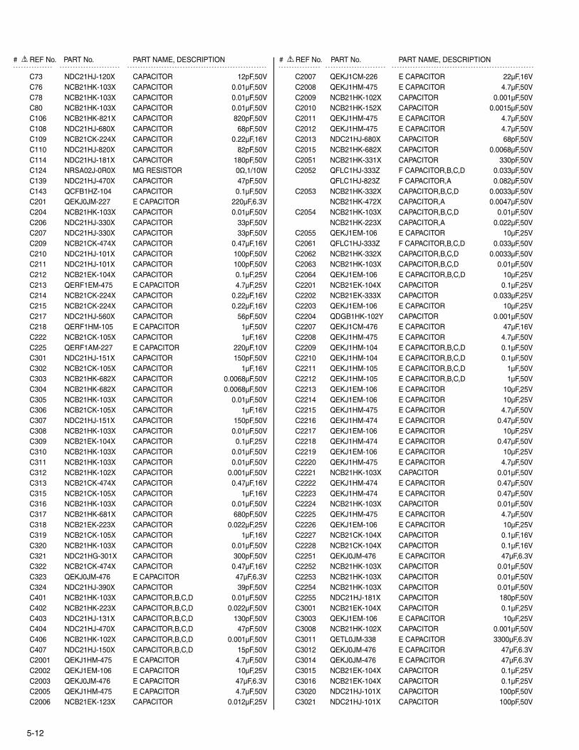
- - - - - - - - - - - - - - - - - - - - - - - - - - - - - - - - - - - - - - - - - - - - - - - - - - - - - - - - - - - - - - - - - - - - - - - - - - - - - - - - - - - - - - - - - - - - - - - - - - - - - - - - - - - - - - - - - - - - - - - - - - - - - - - - - - - - - - - - - - - - - - - - - - - - - - - - - - - - - - - - - - - - - - - - - - - - - - - - - - - - - - - -# REF No. PART No. PART NAME, DESCRIPTION # REF No. PART No. PART NAME, DESCRIPTION
5-12
C73 NDC21HJ-120X CAPACITOR 12pF,50VC76 NCB21HK-103X CAPACITOR 0.01µF,50VC78 NCB21HK-103X CAPACITOR 0.01µF,50VC80 NCB21HK-103X CAPACITOR 0.01µF,50VC106 NCB21HK-821X CAPACITOR 820pF,50VC108 NDC21HJ-680X CAPACITOR 68pF,50VC109 NCB21CK-224X CAPACITOR 0.22µF,16VC110 NDC21HJ-820X CAPACITOR 82pF,50VC114 NDC21HJ-181X CAPACITOR 180pF,50VC124 NRSA02J-0R0X MG RESISTOR 0Ø,1/10WC139 NDC21HJ-470X CAPACITOR 47pF,50VC143 QCFB1HZ-104 CAPACITOR 0.1µF,50VC201 QEKJ0JM-227 E CAPACITOR 220µF,6.3VC204 NCB21HK-103X CAPACITOR 0.01µF,50VC206 NDC21HJ-330X CAPACITOR 33pF,50VC207 NDC21HJ-330X CAPACITOR 33pF,50VC209 NCB21CK-474X CAPACITOR 0.47µF,16VC210 NDC21HJ-101X CAPACITOR 100pF,50VC211 NDC21HJ-101X CAPACITOR 100pF,50VC212 NCB21EK-104X CAPACITOR 0.1µF,25VC213 QERF1EM-475 E CAPACITOR 4.7µF,25VC214 NCB21CK-224X CAPACITOR 0.22µF,16VC215 NCB21CK-224X CAPACITOR 0.22µF,16VC217 NDC21HJ-560X CAPACITOR 56pF,50VC218 QERF1HM-105 E CAPACITOR 1µF,50VC222 NCB21CK-105X CAPACITOR 1µF,16VC225 QERF1AM-227 E CAPACITOR 220µF,10VC301 NDC21HJ-151X CAPACITOR 150pF,50VC302 NCB21CK-105X CAPACITOR 1µF,16VC303 NCB21HK-682X CAPACITOR 0.0068µF,50VC304 NCB21HK-682X CAPACITOR 0.0068µF,50VC305 NCB21HK-103X CAPACITOR 0.01µF,50VC306 NCB21CK-105X CAPACITOR 1µF,16VC307 NDC21HJ-151X CAPACITOR 150pF,50VC308 NCB21HK-103X CAPACITOR 0.01µF,50VC309 NCB21EK-104X CAPACITOR 0.1µF,25VC310 NCB21HK-103X CAPACITOR 0.01µF,50VC311 NCB21HK-103X CAPACITOR 0.01µF,50VC312 NCB21HK-102X CAPACITOR 0.001µF,50VC313 NCB21CK-474X CAPACITOR 0.47µF,16VC315 NCB21CK-105X CAPACITOR 1µF,16VC316 NCB21HK-103X CAPACITOR 0.01µF,50VC317 NCB21HK-681X CAPACITOR 680pF,50VC318 NCB21EK-223X CAPACITOR 0.022µF,25VC319 NCB21CK-105X CAPACITOR 1µF,16VC320 NCB21HK-103X CAPACITOR 0.01µF,50VC321 NDC21HG-301X CAPACITOR 300pF,50VC322 NCB21CK-474X CAPACITOR 0.47µF,16VC323 QEKJ0JM-476 E CAPACITOR 47µF,6.3VC324 NDC21HJ-390X CAPACITOR 39pF,50VC401 NCB21HK-103X CAPACITOR,B,C,D 0.01µF,50VC402 NCB21HK-223X CAPACITOR,B,C,D 0.022µF,50VC403 NDC21HJ-131X CAPACITOR,B,C,D 130pF,50VC404 NDC21HJ-470X CAPACITOR,B,C,D 47pF,50VC406 NCB21HK-102X CAPACITOR,B,C,D 0.001µF,50VC407 NDC21HJ-150X CAPACITOR,B,C,D 15pF,50VC2001 QEKJ1HM-475 E CAPACITOR 4.7µF,50VC2002 QEKJ1EM-106 E CAPACITOR 10µF,25VC2003 QEKJ0JM-476 E CAPACITOR 47µF,6.3VC2005 QEKJ1HM-475 E CAPACITOR 4.7µF,50VC2006 NCB21EK-123X CAPACITOR 0.012µF,25V
C2007 QEKJ1CM-226 E CAPACITOR 22µF,16VC2008 QEKJ1HM-475 E CAPACITOR 4.7µF,50VC2009 NCB21HK-102X CAPACITOR 0.001µF,50VC2010 NCB21HK-152X CAPACITOR 0.0015µF,50VC2011 QEKJ1HM-475 E CAPACITOR 4.7µF,50VC2012 QEKJ1HM-475 E CAPACITOR 4.7µF,50VC2013 NDC21HJ-680X CAPACITOR 68pF,50VC2015 NCB21HK-682X CAPACITOR 0.0068µF,50VC2051 NCB21HK-331X CAPACITOR 330pF,50VC2052 QFLC1HJ-333Z F CAPACITOR,B,C,D 0.033µF,50V
QFLC1HJ-823Z F CAPACITOR,A 0.082µF,50VC2053 NCB21HK-332X CAPACITOR,B,C,D 0.0033µF,50V
NCB21HK-472X CAPACITOR,A 0.0047µF,50VC2054 NCB21HK-103X CAPACITOR,B,C,D 0.01µF,50V
NCB21HK-223X CAPACITOR,A 0.022µF,50VC2055 QEKJ1EM-106 E CAPACITOR 10µF,25VC2061 QFLC1HJ-333Z F CAPACITOR,B,C,D 0.033µF,50VC2062 NCB21HK-332X CAPACITOR,B,C,D 0.0033µF,50VC2063 NCB21HK-103X CAPACITOR,B,C,D 0.01µF,50VC2064 QEKJ1EM-106 E CAPACITOR,B,C,D 10µF,25VC2201 NCB21EK-104X CAPACITOR 0.1µF,25VC2202 NCB21EK-333X CAPACITOR 0.033µF,25VC2203 QEKJ1EM-106 E CAPACITOR 10µF,25VC2204 QDGB1HK-102Y CAPACITOR 0.001µF,50VC2207 QEKJ1CM-476 E CAPACITOR 47µF,16VC2208 QEKJ1HM-475 E CAPACITOR 4.7µF,50VC2209 QEKJ1HM-104 E CAPACITOR,B,C,D 0.1µF,50VC2210 QEKJ1HM-104 E CAPACITOR,B,C,D 0.1µF,50VC2211 QEKJ1HM-105 E CAPACITOR,B,C,D 1µF,50VC2212 QEKJ1HM-105 E CAPACITOR,B,C,D 1µF,50VC2213 QEKJ1EM-106 E CAPACITOR 10µF,25VC2214 QEKJ1EM-106 E CAPACITOR 10µF,25VC2215 QEKJ1HM-475 E CAPACITOR 4.7µF,50VC2216 QEKJ1HM-474 E CAPACITOR 0.47µF,50VC2217 QEKJ1EM-106 E CAPACITOR 10µF,25VC2218 QEKJ1HM-474 E CAPACITOR 0.47µF,50VC2219 QEKJ1EM-106 E CAPACITOR 10µF,25VC2220 QEKJ1HM-475 E CAPACITOR 4.7µF,50VC2221 NCB21HK-103X CAPACITOR 0.01µF,50VC2222 QEKJ1HM-474 E CAPACITOR 0.47µF,50VC2223 QEKJ1HM-474 E CAPACITOR 0.47µF,50VC2224 NCB21HK-103X CAPACITOR 0.01µF,50VC2225 QEKJ1HM-475 E CAPACITOR 4.7µF,50VC2226 QEKJ1EM-106 E CAPACITOR 10µF,25VC2227 NCB21CK-104X CAPACITOR 0.1µF,16VC2228 NCB21CK-104X CAPACITOR 0.1µF,16VC2251 QEKJ0JM-476 E CAPACITOR 47µF,6.3VC2252 NCB21HK-103X CAPACITOR 0.01µF,50VC2253 NCB21HK-103X CAPACITOR 0.01µF,50VC2254 NCB21HK-103X CAPACITOR 0.01µF,50VC2255 NDC21HJ-181X CAPACITOR 180pF,50VC3001 NCB21EK-104X CAPACITOR 0.1µF,25VC3003 QEKJ1EM-106 E CAPACITOR 10µF,25VC3008 NCB21HK-102X CAPACITOR 0.001µF,50VC3011 QETL0JM-338 E CAPACITOR 3300µF,6.3VC3012 QEKJ0JM-476 E CAPACITOR 47µF,6.3VC3014 QEKJ0JM-476 E CAPACITOR 47µF,6.3VC3015 NCB21EK-104X CAPACITOR 0.1µF,25VC3016 NCB21EK-104X CAPACITOR 0.1µF,25VC3020 NDC21HJ-101X CAPACITOR 100pF,50VC3021 NDC21HJ-101X CAPACITOR 100pF,50V

5-13
- - - - - - - - - - - - - - - - - - - - - - - - - - - - - - - - - - - - - - - - - - - - - - - - - - - - - - - - - - - - - - - - - - - - - - - - - - - - - - - - - - - - - - - - - - - - - - - - - - - - - - - - - - - - - - - - - - - - - - - - - - - - - - - - - - - - - - - - - - - - - - - - - - - - - - - - - - - - - - - - - - - - - - - - - - - - - - - - - - - - - - - -# REF No. PART No. PART NAME, DESCRIPTION # REF No. PART No. PART NAME, DESCRIPTION
C3022 NCB21EK-104X CAPACITOR 0.1µF,25VC3024 NDC21HJ-120X CAPACITOR 12pF,50VC3026 NCB21HK-103X CAPACITOR 0.01µF,50VC3027 QEKJ1EM-106 E CAPACITOR 10µF,25VC3030 QEKJ0JM-476 E CAPACITOR 47µF,6.3VC3031 NCB21EK-104X CAPACITOR 0.1µF,25VC3032 NCB21EK-104X CAPACITOR 0.1µF,25VC3033 NCB21EK-104X CAPACITOR 0.1µF,25VC3036 NDC21HJ-180X CAPACITOR 18pF,50VC3037 NDC21HJ-120X CAPACITOR 12pF,50VC3040 NCB21HK-103X CAPACITOR 0.01µF,50VC3041 NDC21HJ-100X CAPACITOR 10pF,50VC3050 NCB21EK-104X CAPACITOR 0.1µF,25VC4002 NCB21EK-104X CAPACITOR 0.1µF,25VC4003 NCB21HK-102X CAPACITOR 0.001µF,50VC4004 QEKJ1AM-226 E CAPACITOR 22µF,10VC4005 NCB21HK-222X CAPACITOR 0.0022µF,50VC4006 QEKJ0JM-476 E CAPACITOR 47µF,6.3VC4007 NCB21HK-102X CAPACITOR,A 0.001µF,50V
NCB21HK-561X CAPACITOR,B,C,D 560pF,50VC4008 NCB21AK-105X CAPACITOR 1µF,10VC4009 NCB21HK-563X CAPACITOR 0.056µF,50VC4010 NCB21EK-223X CAPACITOR 0.022µF,25VC4011 NCB21EK-104X CAPACITOR 0.1µF,25VC4012 NCB21AK-105X CAPACITOR 1µF,10VC4013 NCB21HK-563X CAPACITOR 0.056µF,50VC4014 NDC21HJ-101X CAPACITOR 100pF,50VC4015 NCB21HK-102X CAPACITOR 0.001µF,50V
! C5001 QFZ9073-683 F CAPACITOR 0.068µF,250V! C5002 QFZ9051-333 F CAPACITOR 0.033µF,250V! C5004 QCZ9071-222 CAPACITOR 0.0022µF,250V
C5006 QEZ0375-686 E CAPACITOR 68µF,400VC5101 QCZ0212-472 CAPACITOR 0.0047µF,1kVC5102 QCZ0302-330Z CAPACITOR 33pF,1kVC5104 QEKJ1HM-105 E CAPACITOR 1µF,50VC5105 QFN31HJ-183 F CAPACITOR 0.018µF,50VC5106 QCBB1HJ-271 CAPACITOR 270pF,50VC5107 QFV91HJ-104 F CAPACITOR 0.1µF,50VC5201 QEMU0JM-227 E CAPACITOR 220µF,6.3VC5202 QEMT1CM-687 E CAPACITOR 680µF,16VC5203 QEMT1AM-128 E CAPACITOR 1200µF,10VC5204 QETN2AM-475 E CAPACITOR 4.7µF,100VC5205 QETN1HM-106 E CAPACITOR 10µF,50VC5206 QETN1EM-476 E CAPACITOR 47µF,25VC5207 QETN1CM-107 E CAPACITOR 100µF,16VC5208 QEMU1EM-187 E CAPACITOR 180µF,25VC5301 QEKJ1CM-107 E CAPACITOR 100µF,16VC5302 QEKJ1CM-476 E CAPACITOR 47µF,16VC5303 QEKJ1CM-107 E CAPACITOR 100µF,16VC5304 QFLC1HJ-102Z F CAPACITOR 0.001µF,50VC5305 QFV91HJ-224 F CAPACITOR 0.22µF,50VC5311 NCB21HK-103X CAPACITOR 0.01µF,50VC5351 QUY153-050Y IM BUS WIREC6007 QEMU0JM-227 E CAPACITOR 220µF,6.3VC6008 NCB21HK-103X CAPACITOR 0.01µF,50VC6013 NCB21HK-103X CAPACITOR 0.01µF,50VC6023 NRSA02J-0R0X MG RESISTOR 0Ø,1/10WC6037 QEKJ1EM-106 E CAPACITOR 10µF,25VC6501 QEKJ0JM-107 E CAPACITOR 100µF,6.3VC6502 NCB21HK-103X CAPACITOR 0.01µF,50VC7001 QEKJ0JM-476 E CAPACITOR 47µF,6.3V
C7003 QEKJ0JM-227 E CAPACITOR 220µF,6.3VC7005 NDC21HJ-470X CAPACITOR 47pF,50VC7006 NDC21HJ-330X CAPACITOR 33pF,50VC7007 QEKJ1HM-106 E CAPACITOR 10µF,50VC7008 NCB21HK-102X CAPACITOR 0.001µF,50VC7011 QCFB1HZ-104 CAPACITOR 0.1µF,50VC7165 NCB21HK-681X CAPACITOR 680pF,50VC7167 NCB21HK-681X CAPACITOR 680pF,50VC7202 QETJ0JM-477 E CAPACITOR 470µF,6.3VL1 QQL29BJ-100Z COIL 10µHL2 QQL071J-121Y COIL 120µHL3 QQL29BJ-100Z COIL 10µHL4 QQL29BJ-100Z COIL 10µHL5 QQR0521-012Z NOISE FILTERL12 QQR0967-001 COIL 12µHL13 QQL071J-330Y COIL 33µHL15 QQL29BJ-100Z COIL 10µHL18 QQL071J-220Y COIL 22µHL19 QQL071J-120Y COIL 12µHL20 QUY153-050Y IM BUS WIREL24 QQL071J-270Y COIL 27µHL27 QQL071J-330Y COIL 33µHL28 QQL071J-680Y COIL 68µHL30 QUY153-050Y IM BUS WIREL201 QQL29BK-1R0Z COIL 1.0µHL202 QUY153-050Y IM BUS WIREL203 QQL29BJ-220Z COIL 22µHL204 QQL29BJ-100Z COIL 10µHL206 QQL071J-220Y COIL 22µHL301 QQL29BJ-100Z COIL 10µHL302 QQL231J-6R8Y COIL 6.8µHL303 QQL231J-270Y COIL 27µHL304 QQL29BJ-101Z COIL 100µHL401 QQL071J-150Y COIL,B,C,D 15µHL402 QUY153-050Y IM BUS WIRE,B,C,DL2001 QUY153-050Y IM BUS WIREL2251 QQL29BJ-100Z COIL 10µHL2252 QQL29BJ-151Z COIL 150µHL3001 QUY153-050Y IM BUS WIREL3011 QUY153-050Y IM BUS WIREL3012 QUY153-050Y IM BUS WIREL4001 QUY153-050Y IM BUS WIREL5201 PELN1184 COIL 33µHL5202 PU60944-330K COIL 33µHL6001 QQL29BJ-100Z COIL 10µHL6003 QQL29BJ-470Z COIL 47µHL7201 QQL29BJ-100Z COIL 10µHX1 QAX0576-001Z CRYSTAL RESONATORX2 QCBB1HK-103 CAPACITOR,D 0.01µF,50VX3001 QAX0444-001 CRYSTAL RESONATORX3002 QAX0527-001 CRYSTAL RESONATORS3001 QSW0602-004 PUSH SWITCH,REC SAFETYS3002 QSW0695-001 PUSH SWITCH,S.CASS SWS7001 QSW0456-002Z TACT SWITCH,STAND-BYS7002 QSW0456-002Z TACT SWITCH,SVHS ETS7004 QSW0456-002Z TACT SWITCH,RECS7006 QSW0456-002Z TACT SWITCH,PAUSES7008 QSW0456-002Z TACT SWITCH,STOP/EJECTS7010 QSW0456-002Z TACT SWITCH,PLAYS7012 QSW0456-002Z TACT SWITCH,E.PROGS7016 QSW0456-002Z TACT SWITCH,SAT TIMER

- - - - - - - - - - - - - - - - - - - - - - - - - - - - - - - - - - - - - - - - - - - - - - - - - - - - - - - - - - - - - - - - - - - - - - - - - - - - - - - - - - - - - - - - - - - - - - - - - - - - - - - - - - - - - - - - - - - - - - - - - - - - - - - - - - - - - - - - - - - - - - - - - - - - - - - - - - - - - - - - - - - - - - - - - - - - - - - - - - - - - - - -# REF No. PART No. PART NAME, DESCRIPTION # REF No. PART No. PART NAME, DESCRIPTION
5-14
K2001 NQR0403-003X FERRITE BEADK2002 NQR0403-003X FERRITE BEADK2003 NQR0403-003X FERRITE BEADK2004 NRSA02J-0R0X MG RESISTOR 0Ø,1/10WK2251 NRSA02J-0R0X MG RESISTOR 0Ø,1/10WK2252 NRSA02J-0R0X MG RESISTOR 0Ø,1/10WK2253 NRSA02J-0R0X MG RESISTOR 0Ø,1/10WK5101 QQR0678-001Z FERRITE BEADK5102 QUY153-050Y IM BUS WIREK5301 QUY153-050Y IM BUS WIREK6080 NRSA02J-102X MG RESISTOR 1kØ,1/10WPC3001 GP3S123 IC(PHOTO SENSORPC3002 GP3S123 IC(PHOTO SENSOR
! PC5101 PS2561L1-1/L/ IC(PHOTO COUPLER)T2051 PELN0832 OSC TRANSFORMER,A
PELN0860 OSC TRANSFORMER,B,C,DT2052 PELN0861 OSC TRANSFORMER,B,C,D
! T5001 QQS0033-001 SW TRANSFORMERTU6001 QAU0210-001 TUNERET1 PQ21623-2-5 EARTH PLATE(RF)DI7001 QLF0031-001 FL TUBE,A
QLF0032-001 FL TUBE,B,C,DHD1 PQ35479-1-4 HOLDER(FDP),A
LP30188-001A HOLDER(FDP),B,C,DHS1 LP40621-001A HEAT SINK,Q5101SD1 LP30864-001A SHIELD CASE(PRE)OT1 QYTDSF3010Z SCREW,X2OT2 PU59915-107 #500SPACER,WR1,DOT3 QYTDST3008Z SCREW,Q5101WR1 QUB321-11A1A1 SIN TWIST WIRE,DFC5001 QNG0006-001Z FUSE CLIP,F5001FC5002 QNG0006-001Z FUSE CLIP,F5001J7105 QNN0381-002 PIN JACK,F_IN NI,A,B,C
QNN0383-002 PIN JACK,AU YWR,D! LF5001 PELN1204-01-01 LINE FILTER! LF5002 QQR0978-001 LINE FILTER
CN1 QGF1028C1-11 FPC CONNECTOR,(1-11)U.DRUM,AQGF1028C1-13 FPC CONNECTOR,(1-13)U.DRUM,B,C,D
CN901 QGB2024K1-10S CONNECTOR,(1-10)TERMINALCN902 QGB2024K1-12S CONNECTOR,(1-12)TERMINALCN903 QGB2024K1-10S CONNECTOR,(1-10)TERMINALCN904 QGB2024K1-11S CONNECTOR,(1-11)TERMINALCN905 QGB2024K1-09S CONNECTOR,(1-9)TERMINALCN2001 QGF1207C1-07 FPC CONNECTOR,(1-7)A/C HEADCN2002 QGB2532J1-02 CONNECTOR,(1-2)FE HEADCN3001 QGF1207C1-05 FPC CONNECTOR,(1-5)DRUM MDACN3002 QGB2532J1-02 CONNECTOR,(1-2)LOADING MOTORCN3003 QGB2015M2-08 CONNECTOR,(1-8)CAPSTAN MOTORCN3004 QGB2534J2-04 CONNECTOR,(1-4)ROTARY ENCODER
! CN5001 QGA7901C3-02 CONNECTOR,(1-2)AC INCN7001 QGF1207C1-09 FPC CONNECTOR,(1-9)ADV.JOG
! CP3002 ICP-N25 CIRCUIT PROTECTORCP4001 QUY153-050Y IM BUS WIRE
! CP5303 NMFZ012-1R5X-M FUSE T1.5A,50V! CP5304 NMFZ012-1R0X-M FUSE T1.0A,50V! F5001 QMF51E2-2R0J1 FUSE T2.0A,AC250V
******************************2D DIGITAL BOARD ASSEMBLY <05>(MODEL:A,B,C)
PW1 LPA10090-07A 2D DIGITAL BOARD ASSYIC1201 JCP8036 IC
! Q1201 2SC1317/RS/-T TRANSISTORQ1202 2SA1576A/QR/-X TRANSISTOR
or 2PA1576/R/-X TRANSISTORQ1203 2SA1576A/QR/-X TRANSISTOR
or 2PA1576/R/-X TRANSISTORQ1204 2SC4081/QRS/-X TRANSISTOR
or 2PC4081/R/-X TRANSISTORQ1205 2SC4081/S/-X TRANSISTORQ1206 2SC4081/QRS/-X TRANSISTOR
or 2PC4081/R/-X TRANSISTORD1201 RD4.3ES/B3/-T2 ZENER DIODED1202 QUY153-050Y IM BUS WIRER1201 NRSA02J-121X MG RESISTOR 120Ø,1/10WR1202 NRSA02J-101X MG RESISTOR 100Ø,1/10WR1203 NRSA02J-221X MG RESISTOR 220Ø,1/10WR1204 NRSA02J-221X MG RESISTOR 220Ø,1/10WR1205 NRSA02J-102X MG RESISTOR 1kØ,1/10WR1206 NRSA02J-561X MG RESISTOR 560Ø,1/10WR1207 NRSA02J-562X MG RESISTOR 5.6kØ,1/10WR1208 NRSA02J-123X MG RESISTOR 12kØ,1/10WR1209 NRSA02J-180X MG RESISTOR 18Ø,1/10WR1210 NRSA02J-393X MG RESISTOR 39kØ,1/10WR1211 NRSA02J-103X MG RESISTOR 10kØ,1/10WR1212 NRSA02J-102X MG RESISTOR 1kØ,1/10WR1213 NRSA02J-331X MG RESISTOR 330Ø,1/10WR1214 NRSA02J-101X MG RESISTOR 100Ø,1/10WR1215 NRSA02J-102X MG RESISTOR 1kØ,1/10WR1216 NRSA02J-331X MG RESISTOR 330Ø,1/10WR1217 NRSA02J-101X MG RESISTOR 100Ø,1/10WR1218 NRSA02J-301X MG RESISTOR 300Ø,1/10WR1222 NRSA02J-471X MG RESISTOR 470Ø,1/10WR1224 NRSA02J-561X MG RESISTOR 560Ø,1/10WR1225 NRSA02J-273X MG RESISTOR 27kØ,1/10WR1226 NRSA02J-153X MG RESISTOR 15kØ,1/10WR1227 NRSA02J-561X MG RESISTOR 560Ø,1/10WR1228 NRSA02J-391X MG RESISTOR 390Ø,1/10WR1230 NRSA02J-0R0X MG RESISTOR 0Ø,1/10WR1231 NRSA02J-0R0X MG RESISTOR 0Ø,1/10WR1232 NRSA02J-0R0X MG RESISTOR 0Ø,1/10WR1233 NRSA02J-0R0X MG RESISTOR 0Ø,1/10WVR1201 QVZ3521-103Z V RESISTOR,D/A LEVEL ADJB1204 NRSA02J-0R0X MG RESISTOR 0Ø,1/10WC1201 QEKJ0JM-476 E CAPACITOR 47µF,6.3VC1208 NDC21HJ-101X CAPACITOR 100pF,50VC1210 NDC21HJ-330X CAPACITOR 33pF,50VC1211 QEKJ0JM-476 E CAPACITOR 47µF,6.3VC1212 NCB21HK-102X CAPACITOR 0.001µF,50VC1213 NCF21EZ-104X CAPACITOR 0.1µF,25VC1214 NCF21CZ-105X CAPACITOR 1µF,16VC1215 QEKJ0JM-476 E CAPACITOR 47µF,6.3VC1216 NCF21EZ-104X CAPACITOR 0.1µF,25VC1217 NCF21EZ-104X CAPACITOR 0.1µF,25VC1218 NCF21EZ-104X CAPACITOR 0.1µF,25VC1219 NCF21CZ-105X CAPACITOR 1µF,16VC1220 QEKJ0JM-476 E CAPACITOR 47µF,6.3V
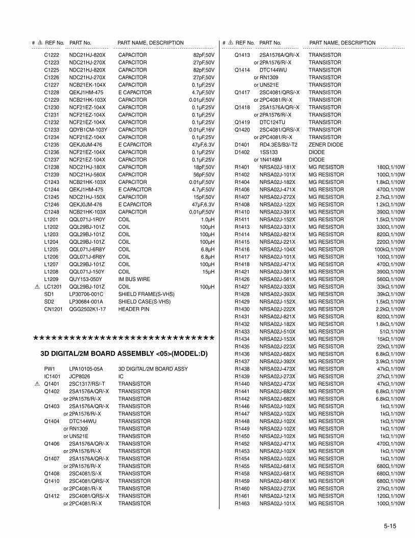
5-15
- - - - - - - - - - - - - - - - - - - - - - - - - - - - - - - - - - - - - - - - - - - - - - - - - - - - - - - - - - - - - - - - - - - - - - - - - - - - - - - - - - - - - - - - - - - - - - - - - - - - - - - - - - - - - - - - - - - - - - - - - - - - - - - - - - - - - - - - - - - - - - - - - - - - - - - - - - - - - - - - - - - - - - - - - - - - - - - - - - - - - - - -# REF No. PART No. PART NAME, DESCRIPTION # REF No. PART No. PART NAME, DESCRIPTION
C1222 NDC21HJ-820X CAPACITOR 82pF,50VC1223 NDC21HJ-270X CAPACITOR 27pF,50VC1225 NDC21HJ-820X CAPACITOR 82pF,50VC1226 NDC21HJ-270X CAPACITOR 27pF,50VC1227 NCB21EK-104X CAPACITOR 0.1µF,25VC1228 QEKJ1HM-475 E CAPACITOR 4.7µF,50VC1229 NCB21HK-103X CAPACITOR 0.01µF,50VC1230 NCF21EZ-104X CAPACITOR 0.1µF,25VC1231 NCF21EZ-104X CAPACITOR 0.1µF,25VC1232 NCF21EZ-104X CAPACITOR 0.1µF,25VC1233 QDYB1CM-103Y CAPACITOR 0.01µF,16VC1234 NCF21EZ-104X CAPACITOR 0.1µF,25VC1235 QEKJ0JM-476 E CAPACITOR 47µF,6.3VC1236 NCF21EZ-104X CAPACITOR 0.1µF,25VC1237 NCF21EZ-104X CAPACITOR 0.1µF,25VC1238 NDC21HJ-180X CAPACITOR 18pF,50VC1239 NDC21HJ-560X CAPACITOR 56pF,50VC1243 NCB21HK-103X CAPACITOR 0.01µF,50VC1244 QEKJ1HM-475 E CAPACITOR 4.7µF,50VC1245 NDC21HJ-150X CAPACITOR 15pF,50VC1246 QEKJ0JM-476 E CAPACITOR 47µF,6.3VC1248 NCB21HK-103X CAPACITOR 0.01µF,50VL1201 QQL071J-1R0Y COIL 1.0µHL1202 QQL29BJ-101Z COIL 100µHL1203 QQL29BJ-101Z COIL 100µHL1204 QQL29BJ-101Z COIL 100µHL1205 QQL071J-6R8Y COIL 6.8µHL1206 QQL071J-6R8Y COIL 6.8µHL1207 QQL29BJ-101Z COIL 100µHL1208 QQL071J-150Y COIL 15µHL1209 QUY153-050Y IM BUS WIRE
! LC1201 QQL29BJ-101Z COIL 100µHSD1 LP30706-001C SHIELD FRAME(S-VHS)SD2 LP30684-001A SHIELD CASE(S-VHS)CN1201 QGG2502K1-17 HEADER PIN
******************************3D DIGITAL/2M BOARD ASSEMBLY <05>(MODEL:D)
PW1 LPA10105-05A 3D DIGITAL/2M BOARD ASSYIC1401 JCP8026 IC
! Q1401 2SC1317/RS/-T TRANSISTORQ1402 2SA1576A/QR/-X TRANSISTOR
or 2PA1576/R/-X TRANSISTORQ1403 2SA1576A/QR/-X TRANSISTOR
or 2PA1576/R/-X TRANSISTORQ1404 DTC144WU TRANSISTOR
or RN1309 TRANSISTORor UN521E TRANSISTOR
Q1406 2SA1576A/QR/-X TRANSISTORor 2PA1576/R/-X TRANSISTOR
Q1407 2SA1576A/QR/-X TRANSISTORor 2PA1576/R/-X TRANSISTOR
Q1408 2SC4081/S/-X TRANSISTORQ1410 2SC4081/QRS/-X TRANSISTOR
or 2PC4081/R/-X TRANSISTORQ1412 2SC4081/QRS/-X TRANSISTOR
or 2PC4081/R/-X TRANSISTOR
Q1413 2SA1576A/QR/-X TRANSISTORor 2PA1576/R/-X TRANSISTOR
Q1414 DTC144WU TRANSISTORor RN1309 TRANSISTORor UN521E TRANSISTOR
Q1417 2SC4081/QRS/-X TRANSISTORor 2PC4081/R/-X TRANSISTOR
Q1418 2SA1576A/QR/-X TRANSISTORor 2PA1576/R/-X TRANSISTOR
Q1419 DTC124TU TRANSISTORQ1420 2SC4081/QRS/-X TRANSISTOR
or 2PC4081/R/-X TRANSISTORD1401 RD4.3ES/B3/-T2 ZENER DIODED1402 1SS133 DIODE
or 1N4148M DIODER1401 NRSA02J-181X MG RESISTOR 180Ø,1/10WR1402 NRSA02J-101X MG RESISTOR 100Ø,1/10WR1404 NRSA02J-182X MG RESISTOR 1.8kØ,1/10WR1406 NRSA02J-471X MG RESISTOR 470Ø,1/10WR1407 NRSA02J-272X MG RESISTOR 2.7kØ,1/10WR1408 NRSA02J-122X MG RESISTOR 1.2kØ,1/10WR1410 NRSA02J-391X MG RESISTOR 390Ø,1/10WR1411 NRSA02J-152X MG RESISTOR 1.5kØ,1/10WR1413 NRSA02J-331X MG RESISTOR 330Ø,1/10WR1414 NRSA02J-821X MG RESISTOR 820Ø,1/10WR1415 NRSA02J-221X MG RESISTOR 220Ø,1/10WR1416 NRSA02J-104X MG RESISTOR 100kØ,1/10WR1417 NRSA02J-101X MG RESISTOR 100Ø,1/10WR1418 NRSA02J-471X MG RESISTOR 470Ø,1/10WR1421 NRSA02J-391X MG RESISTOR 390Ø,1/10WR1426 NRSA02J-561X MG RESISTOR 560Ø,1/10WR1427 NRSA02J-333X MG RESISTOR 33kØ,1/10WR1428 NRSA02J-393X MG RESISTOR 39kØ,1/10WR1429 NRSA02J-152X MG RESISTOR 1.5kØ,1/10WR1430 NRSA02J-222X MG RESISTOR 2.2kØ,1/10WR1431 NRSA02J-821X MG RESISTOR 820Ø,1/10WR1432 NRSA02J-182X MG RESISTOR 1.8kØ,1/10WR1433 NRSA02J-510X MG RESISTOR 51Ø,1/10WR1434 NRSA02J-153X MG RESISTOR 15kØ,1/10WR1435 NRSA02J-223X MG RESISTOR 22kØ,1/10WR1436 NRSA02J-682X MG RESISTOR 6.8kØ,1/10WR1437 NRSA02J-392X MG RESISTOR 3.9kØ,1/10WR1438 NRSA02J-473X MG RESISTOR 47kØ,1/10WR1439 NRSA02J-273X MG RESISTOR 27kØ,1/10WR1440 NRSA02J-473X MG RESISTOR 47kØ,1/10WR1441 NRSA02J-682X MG RESISTOR 6.8kØ,1/10WR1442 NRSA02J-682X MG RESISTOR 6.8kØ,1/10WR1446 NRSA02J-102X MG RESISTOR 1kØ,1/10WR1447 NRSA02J-102X MG RESISTOR 1kØ,1/10WR1448 NRSA02J-102X MG RESISTOR 1kØ,1/10WR1449 NRSA02J-102X MG RESISTOR 1kØ,1/10WR1450 NRSA02J-102X MG RESISTOR 1kØ,1/10WR1452 NRSA02J-471X MG RESISTOR 470Ø,1/10WR1453 NRSA02J-102X MG RESISTOR 1kØ,1/10WR1454 NRSA02J-102X MG RESISTOR 1kØ,1/10WR1455 NRSA02J-681X MG RESISTOR 680Ø,1/10WR1458 NRSA02J-681X MG RESISTOR 680Ø,1/10WR1459 NRSA02J-681X MG RESISTOR 680Ø,1/10WR1460 NRSA02J-273X MG RESISTOR 27kØ,1/10WR1461 NRSA02J-121X MG RESISTOR 120Ø,1/10WR1463 NRSA02J-101X MG RESISTOR 100Ø,1/10W

- - - - - - - - - - - - - - - - - - - - - - - - - - - - - - - - - - - - - - - - - - - - - - - - - - - - - - - - - - - - - - - - - - - - - - - - - - - - - - - - - - - - - - - - - - - - - - - - - - - - - - - - - - - - - - - - - - - - - - - - - - - - - - - - - - - - - - - - - - - - - - - - - - - - - - - - - - - - - - - - - - - - - - - - - - - - - - - - - - - - - - - -# REF No. PART No. PART NAME, DESCRIPTION # REF No. PART No. PART NAME, DESCRIPTION
5-16
VR1401 QVZ3521-103Z V RESISTOR,D/A LEVEL ADJB1412 NRSA02J-0R0X MG RESISTOR 0Ø,1/10WC1401 QEKJ1CM-336 E CAPACITOR 33µF,16VC1402 NCB21HK-103X CAPACITOR 0.01µF,50VC1403 QEKJ0JM-337 E CAPACITOR 330µF,6.3VC1404 NCF21EZ-104X CAPACITOR 0.1µF,25VC1405 NCF21EZ-104X CAPACITOR 0.1µF,25VC1406 NCB21HK-103X CAPACITOR 0.01µF,50VC1407 NDC21HJ-680X CAPACITOR 68pF,50VC1408 NDC21HJ-330X CAPACITOR 33pF,50VC1410 QEKJ1EM-475 E CAPACITOR 4.7µF,25VC1411 NCF21EZ-104X CAPACITOR 0.1µF,25VC1412 NDC21HJ-680X CAPACITOR 68pF,50VC1413 NDC21HJ-330X CAPACITOR 33pF,50VC1415 NCF21EZ-104X CAPACITOR 0.1µF,25VC1416 QEKJ1CM-106 E CAPACITOR 10µF,16VC1417 NCF21EZ-104X CAPACITOR 0.1µF,25VC1421 NDC21HJ-330X CAPACITOR 33pF,50VC1422 NDC21HJ-680X CAPACITOR 68pF,50VC1423 NCF21EZ-104X CAPACITOR 0.1µF,25VC1424 NCB21HK-103X CAPACITOR 0.01µF,50VC1425 NCB21HK-103X CAPACITOR 0.01µF,50VC1426 NDC21HJ-390X CAPACITOR 39pF,50VC1428 NDC21HJ-220X CAPACITOR 22pF,50VC1429 QEKJ0JM-337 E CAPACITOR 330µF,6.3VC1430 NCF21EZ-104X CAPACITOR 0.1µF,25VC1432 NCF21CZ-105X CAPACITOR 1µF,16VC1433 NCF21EZ-104X CAPACITOR 0.1µF,25VC1435 NCF21EZ-104X CAPACITOR 0.1µF,25VC1436 NCF21EZ-104X CAPACITOR 0.1µF,25VC1437 NCF21EZ-104X CAPACITOR 0.1µF,25VC1438 NCF21EZ-104X CAPACITOR 0.1µF,25VC1439 NCF21CZ-105X CAPACITOR 1µF,16VC1440 NCF21EZ-104X CAPACITOR 0.1µF,25VC1441 NCF21EZ-104X CAPACITOR 0.1µF,25VC1442 NCF21CZ-105X CAPACITOR 1µF,16VC1444 NCF21EZ-104X CAPACITOR 0.1µF,25VC1445 NCF21EZ-104X CAPACITOR 0.1µF,25VC1446 QEKJ0JM-476 E CAPACITOR 47µF,6.3VC1447 NCF21EZ-104X CAPACITOR 0.1µF,25VC1448 QEKJ0JM-476 E CAPACITOR 47µF,6.3VC1449 NCF21EZ-104X CAPACITOR 0.1µF,25VC1450 NCF21EZ-104X CAPACITOR 0.1µF,25VC1451 QEKJ1EM-475 E CAPACITOR 4.7µF,25VC1452 NCF21EZ-104X CAPACITOR 0.1µF,25VC1453 NCF21EZ-104X CAPACITOR 0.1µF,25VC1454 NCF21EZ-104X CAPACITOR 0.1µF,25VC1455 NCF21EZ-104X CAPACITOR 0.1µF,25VC1463 QEKJ0JM-336 E CAPACITOR 33µF,6.3VC1468 NDC21HJ-101X CAPACITOR 100pF,50VC1470 NDC21HJ-330X CAPACITOR 33pF,50VC1471 NCF21EZ-104X CAPACITOR 0.1µF,25VC1472 NCF21EZ-104X CAPACITOR 0.1µF,25VC1473 NCF21EZ-104X CAPACITOR 0.1µF,25VL1401 QQL29BJ-100Z COIL 10µHL1402 QQL071J-6R8Y COIL 6.8µHL1403 QQL071J-6R8Y COIL 6.8µHL1404 QQL071J-6R8Y COIL 6.8µHL1405 QQL01BJ-101Z COIL 100µHL1406 QQL071J-330Y COIL 33µHL1407 QQL01BJ-101Z COIL 100µH
L1409 QQL071J-1R0Y COIL 1.0µHLC1401 QQR0521-007Z NOISE FILTERLC1402 QQR0521-006Z NOISE FILTERSD1 LP30706-001C SHIELD FRAME(S-VHS)SD2 LP30684-001A SHIELD CASE(S-VHS)CN1401 QGG2502K1-17 HEADER PIN
******************************TERMINAL BOARD ASSEMBLY <06>
PW1 LPA10138-05A TERMINAL BOARD ASSY,ALPA10138-03B TERMINAL BOARD ASSY,B,C,D
IC501 JCP8018 ICor JCP8028 ICor JCP8028-01 ICor JCP8038 IC
IC502 VC2076DP ICIC901 BH7636S ICQ901 UN5211 TRANSISTOR
or RN1302 TRANSISTORor DTC114EU TRANSISTORor PDTC114EU TRANSISTOR
Q902 2SB1218A/QR/-X TRANSISTORor 2PA1576/R/-X TRANSISTORor 2SA1576A/QR/-X TRANSISTOR
Q903 2SB1218A/QR/-X TRANSISTOR,B,C,Dor 2PA1576/R/-X TRANSISTOR,B,C,Dor 2SA1576A/QR/-X TRANSISTOR,B,C,D
Q904 2SB1218A/QR/-X TRANSISTOR,B,C,Dor 2PA1576/R/-X TRANSISTOR,B,C,Dor 2SA1576A/QR/-X TRANSISTOR,B,C,D
Q905 UN521E TRANSISTORor DTC144WU TRANSISTORor PDTC144WU TRANSISTORor RN1309 TRANSISTOR
Q906 2SD1819A/QRS/-X TRANSISTORor 2SC4081/QRS/-X TRANSISTORor 2PC4081/R/-X TRANSISTOR
Q907 2SD1819A/QRS/-X TRANSISTORor 2PC4081/R/-X TRANSISTORor 2SC4081/QRS/-X TRANSISTOR
Q908 2SD1819A/QRS/-X TRANSISTORor 2SC4081/QRS/-X TRANSISTORor 2PC4081/R/-X TRANSISTOR
Q909 2SB1218A/QR/-X TRANSISTORor 2PA1576/R/-X TRANSISTORor 2SA1576A/QR/-X TRANSISTOR
Q910 2SB1218A/QR/-X TRANSISTORor 2SA1576A/QR/-X TRANSISTORor 2PA1576/R/-X TRANSISTOR
Q911 UN521E TRANSISTORor RN1309 TRANSISTORor DTC144WU TRANSISTORor PDTC144WU TRANSISTOR
Q912 UN5215 TRANSISTORor RN1311 TRANSISTORor DTC114TU TRANSISTORor PDTC114TU TRANSISTOR

5-17
- - - - - - - - - - - - - - - - - - - - - - - - - - - - - - - - - - - - - - - - - - - - - - - - - - - - - - - - - - - - - - - - - - - - - - - - - - - - - - - - - - - - - - - - - - - - - - - - - - - - - - - - - - - - - - - - - - - - - - - - - - - - - - - - - - - - - - - - - - - - - - - - - - - - - - - - - - - - - - - - - - - - - - - - - - - - - - - - - - - - - - - -# REF No. PART No. PART NAME, DESCRIPTION # REF No. PART No. PART NAME, DESCRIPTION
R503 NRSA02J-221X MG RESISTOR 220Ø,1/10WR504 NRSA02J-332X MG RESISTOR 3.3kØ,1/10WR505 NRSA02J-392X MG RESISTOR 3.9kØ,1/10WR506 NRSA02J-391X MG RESISTOR 390Ø,1/10WR507 NRSA02J-122X MG RESISTOR 1.2kØ,1/10WR508 NRSA02J-151X MG RESISTOR 150Ø,1/10WR509 NRSA02J-162X MG RESISTOR 1.6kØ,1/10WR510 NRVA02D-102X CMF RESISTOR 1kØ,1/10WR511 NRVA02D-471X CMF RESISTOR 470Ø,1/10WR512 NRVA02D-102X CMF RESISTOR 1kØ,1/10WR513 NRVA02D-152X CMF RESISTOR 1.5kØ,1/10WR514 NRVA02D-332X CMF RESISTOR 3.3kØ,1/10WR515 NRVA02D-332X CMF RESISTOR 3.3kØ,1/10WR516 QUY160-100Y IM BUS WIRER517 QUY160-100Y IM BUS WIRER525 QRE141J-125Y RESISTOR 1.2MØ,1/4WR531 NRSA02J-101X MG RESISTOR 100Ø,1/10WR532 NRSA02J-101X MG RESISTOR 100Ø,1/10WR533 NRSA02J-101X MG RESISTOR 100Ø,1/10WR534 NRSA02J-101X MG RESISTOR 100Ø,1/10WR535 NRSA02J-101X MG RESISTOR 100Ø,1/10WR536 NRSA02J-101X MG RESISTOR 100Ø,1/10WR901 NRSA02J-750X MG RESISTOR 75Ø,1/10WR902 NRSA02J-750X MG RESISTOR 75Ø,1/10WR903 QRE141J-680Y RESISTOR 68Ø,1/4WR904 NQL402M-4R7X INDUCTORR905 NQL402M-4R7X INDUCTORR906 QQL231J-100Y COIL 10µHR907 QQL231J-100Y COIL 10µHR908 NRSA02J-0R0X MG RESISTOR 0Ø,1/10WR909 NRSA02J-750X MG RESISTOR 75Ø,1/10WR910 NRSA02J-750X MG RESISTOR 75Ø,1/10WR911 NRSA02J-750X MG RESISTOR 75Ø,1/10WR912 NRSA02J-101X MG RESISTOR 100Ø,1/10WR913 NRSA02J-101X MG RESISTOR 100Ø,1/10WR914 QQL231J-100Y COIL 10µHR915 QQL231J-100Y COIL 10µHR916 NRSA02J-102X MG RESISTOR 1kØ,1/10WR917 NRSA02J-0R0X MG RESISTOR 0Ø,1/10WR918 NRSA02J-0R0X MG RESISTOR 0Ø,1/10WR919 QRE141J-101Y RESISTOR,B,C,D 100Ø,1/4WR920 QRE141J-101Y RESISTOR,B,C,D 100Ø,1/4WR921 QRE121J-391Y RESISTOR,B,C,D 390Ø,1/2WR922 QRE121J-391Y RESISTOR,B,C,D 390Ø,1/2WR923 NRSA02J-750X MG RESISTOR,B,C,D 75Ø,1/10WR924 NRSA02J-750X MG RESISTOR,B,C,D 75Ø,1/10WR929 NRSA02J-820X MG RESISTOR 82Ø,1/10WR930 NRSA02J-750X MG RESISTOR 75Ø,1/10WR931 NRSA02J-101X MG RESISTOR 100Ø,1/10WR932 NRSA02J-511X MG RESISTOR 510Ø,1/10WR933 NRSA02J-471X MG RESISTOR 470Ø,1/10WR934 QRE141J-101Y RESISTOR 100Ø,1/4WR935 QRE141J-101Y RESISTOR 100Ø,1/4WR936 QRE141J-101Y RESISTOR 100Ø,1/4WR937 QRE141J-101Y RESISTOR 100Ø,1/4WR938 QRE141J-101Y RESISTOR 100Ø,1/4WR939 QRE141J-101Y RESISTOR 100Ø,1/4WR940 NRSA02J-103X MG RESISTOR 10kØ,1/10WR941 NRSA02J-332X MG RESISTOR 3.3kØ,1/10WR942 NRSA02J-472X MG RESISTOR 4.7kØ,1/10WR943 NRSA02J-0R0X MG RESISTOR 0Ø,1/10W
R944 NRSA02J-272X MG RESISTOR 2.7kØ,1/10WR945 NRSA02J-102X MG RESISTOR 1kØ,1/10WR946 NRSA02J-561X MG RESISTOR 560Ø,1/10WR947 NRSA02J-682X MG RESISTOR 6.8kØ,1/10WR949 QRE121J-331Y RESISTOR 330Ø,1/2WR951 NRSA02J-332X MG RESISTOR 3.3kØ,1/10WR952 NRSA02J-562X MG RESISTOR 5.6kØ,1/10WR953 NRSA02J-562X MG RESISTOR 5.6kØ,1/10WR964 NRSA02J-101X MG RESISTOR 100Ø,1/10WC501 QEKJ1HM-225 E CAPACITOR 2.2µF,50VC502 QEKJ1HM-475 E CAPACITOR 4.7µF,50VC503 QEKJ1HM-225 E CAPACITOR 2.2µF,50VC504 NCB21EK-104X CAPACITOR 0.1µF,25VC505 QEKJ1HM-475 E CAPACITOR 4.7µF,50VC506 NCB21HK-103X CAPACITOR 0.01µF,50VC507 QEKJ0JM-476 E CAPACITOR 47µF,6.3VC508 QEKJ1HM-474 E CAPACITOR 0.47µF,50VC509 QEKJ1CM-106 E CAPACITOR 10µF,16VC510 QEKJ0JM-476 E CAPACITOR 47µF,6.3VC511 NCB21HK-103X CAPACITOR 0.01µF,50VC512 NCB21HK-103X CAPACITOR 0.01µF,50VC513 QEKJ1HM-475 E CAPACITOR 4.7µF,50VC514 NCB21HK-103X CAPACITOR 0.01µF,50VC515 NCB21HK-103X CAPACITOR 0.01µF,50VC516 NCB21HK-103X CAPACITOR 0.01µF,50VC518 NCB21EK-104X CAPACITOR 0.1µF,25VC519 QEKJ1HM-225 E CAPACITOR 2.2µF,50VC520 QEKJ1HM-475 E CAPACITOR 4.7µF,50VC521 QEKJ1HM-475 E CAPACITOR 4.7µF,50VC522 QEKJ1HM-225 E CAPACITOR 2.2µF,50VC523 QEKJ1HM-225 E CAPACITOR 2.2µF,50VC524 NDC21HG-301X CAPACITOR 300pF,50VC525 NDC21HG-301X CAPACITOR 300pF,50VC526 NDC21HJ-101X CAPACITOR 100pF,50VC527 NDC21HJ-181X CAPACITOR 180pF,50VC528 NDC21HG-271X CAPACITOR 270pF,50VC529 NDC21HG-820X CAPACITOR 82pF,50VC530 NDC21HG-221X CAPACITOR 220pF,50VC531 NDC21HG-301X CAPACITOR 300pF,50VC532 NDC21HG-301X CAPACITOR 300pF,50VC533 NCB21HK-103X CAPACITOR 0.01µF,50VC534 QEKJ0JM-476 E CAPACITOR 47µF,6.3VC535 NCB21HK-103X CAPACITOR 0.01µF,50VC551 QEKJ1HM-105 E CAPACITOR 1µF,50VC553 QCBB1HK-103 CAPACITOR 0.01µF,50VC554 QEKJ1HM-105 E CAPACITOR 1µF,50VC556 QCBB1HK-103 CAPACITOR 0.01µF,50VC557 QEKJ1HM-105 E CAPACITOR 1µF,50VC559 NCB21HK-103X CAPACITOR 0.01µF,50VC560 QEKJ1HM-105 E CAPACITOR 1µF,50VC561 QEKJ1HM-105 E CAPACITOR 1µF,50VC562 QEKJ1HM-105 E CAPACITOR 1µF,50VC564 NCB21HK-103X CAPACITOR 0.01µF,50VC566 NCB21HK-103X CAPACITOR 0.01µF,50VC568 NDC21HJ-680X CAPACITOR 68pF,50VC569 NDC21HJ-680X CAPACITOR 68pF,50VC570 NDC21HJ-680X CAPACITOR 68pF,50VC571 NDC21HJ-680X CAPACITOR 68pF,50VC572 NDC21HJ-680X CAPACITOR 68pF,50VC573 NDC21HJ-680X CAPACITOR 68pF,50VC575 NDC21HJ-101X CAPACITOR 100pF,50V
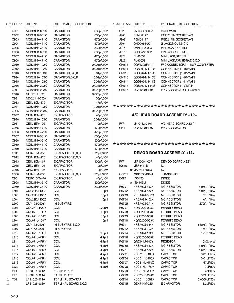
- - - - - - - - - - - - - - - - - - - - - - - - - - - - - - - - - - - - - - - - - - - - - - - - - - - - - - - - - - - - - - - - - - - - - - - - - - - - - - - - - - - - - - - - - - - - - - - - - - - - - - - - - - - - - - - - - - - - - - - - - - - - - - - - - - - - - - - - - - - - - - - - - - - - - - - - - - - - - - - - - - - - - - - - - - - - - - - - - - - - - - - -# REF No. PART No. PART NAME, DESCRIPTION # REF No. PART No. PART NAME, DESCRIPTION
5-18
C901 NCB21HK-331X CAPACITOR 330pF,50VC902 NCB21HK-331X CAPACITOR 330pF,50VC903 NCB21HK-471X CAPACITOR 470pF,50VC904 NCB21HK-471X CAPACITOR 470pF,50VC905 NCB21HK-331X CAPACITOR 330pF,50VC906 NCB21HK-331X CAPACITOR 330pF,50VC907 NCB21HK-471X CAPACITOR 470pF,50VC908 NCB21HK-471X CAPACITOR 470pF,50VC910 NCB21HK-102X CAPACITOR 0.001µF,50VC912 NCB21HK-102X CAPACITOR 0.001µF,50VC913 NCB21HK-103X CAPACITOR,B,C,D 0.01µF,50VC914 NCB21HK-103X CAPACITOR,B,C,D 0.01µF,50VC915 NCB21HK-103X CAPACITOR 0.01µF,50VC916 NCB21HK-223X CAPACITOR 0.022µF,50VC917 NCB21HK-223X CAPACITOR 0.022µF,50VC918 QCBB1HK-223 CAPACITOR 0.022µF,50VC921 NDC21HJ-330X CAPACITOR 33pF,50VC923 QEKJ1CM-476 E CAPACITOR 47µF,16VC924 NCB21HK-103X CAPACITOR 0.01µF,50VC925 NCB21HK-223X CAPACITOR 0.022µF,50VC927 QEKJ1CM-476 E CAPACITOR 47µF,16VC928 NCB21HK-103X CAPACITOR 0.01µF,50VC931 QEKJ1EM-106 E CAPACITOR 10µF,25VC935 NCB21HK-471X CAPACITOR 470pF,50VC936 NCB21HK-471X CAPACITOR 470pF,50VC937 NCB21HK-331X CAPACITOR 330pF,50VC938 NCB21HK-331X CAPACITOR 330pF,50VC939 NCB21HK-471X CAPACITOR 470pF,50VC940 NCB21HK-471X CAPACITOR 470pF,50VC941 QEKJ0JM-227 E CAPACITOR,B,C,D 220µF,6.3VC942 QEKJ1CM-476 E CAPACITOR,B,C,D 47µF,16VC943 QEKJ1CM-107 E CAPACITOR 100µF,16VC945 QEKJ1EM-106 E CAPACITOR 10µF,25VC946 QEKJ1EM-106 E CAPACITOR 10µF,25VC950 QEKJ0JM-227 E CAPACITOR,B,C,D 220µF,6.3VC951 QEKC1CM-476 E CAPACITOR 47µF,16VC958 NCB21HK-331X CAPACITOR 330pF,50VC959 NCB21HK-331X CAPACITOR 330pF,50VL501 QQL29BJ-100Z COIL 10µHL503 QQL29BJ-100Z COIL 10µHL504 QQL29BJ-100Z COIL 10µHL505 QUY153-050Y IM BUS WIREL901 QQL231J-R22Y COIL 0.22µHL902 QQL071J-1R0Y COIL 1.0µHL903 QQL071J-150Y COIL 15µHL904 QQL071J-150Y COIL 15µHL906 QUY153-050Y IM BUS WIRE,B,C,DL907 QUY153-050Y IM BUS WIREL910 QQL071J-1R0Y COIL 1.0µHL913 QQL071J-4R7Y COIL 4.7µHL914 QQL071J-4R7Y COIL 4.7µHL915 QQL071J-4R7Y COIL 4.7µHL916 QQL071J-4R7Y COIL 4.7µHL917 QQL071J-4R7Y COIL 4.7µHL918 QQL071J-4R7Y COIL 4.7µHL919 QQL071J-4R7Y COIL 4.7µHL920 QQL071J-4R7Y COIL 4.7µHET1 LP30918-001A EARTH PLATEET2 LP30915-001A EARTH PLATE
! TB1 LP21028-001A TERMINAL BOARD,A! LP21028-002A TERMINAL BOARD,B,C,D
OT1 QYTDSF3008Z SCREW,X6J901 PEMC1177 RGB21PIN SOCKET,AV1J902 PEMC1177 RGB21PIN SOCKET,AV2J904 QND0084-001 S JACK,S OUT,B,C,DJ915 QNN0418-003 PIN JACK,A.OUT(L)J916 QNN0418-002 PIN JACK,A.OUT(R)J921 PU60659 MINI JACK,SAT.CTLJ922 PU60659 MINI JACK,PAUSE/RAE,B,C,DCN511 QGF1208F1-11 FPC CONNECTOR,(1-11)S/P CONVERTERCN911 QGB2024J1-10S CONNECTOR,(1-10)MAINCN912 QGB2024J1-12S CONNECTOR,(1-12)MAINCN913 QGB2024J1-10S CONNECTOR,(1-10)MAINCN914 QGB2024J1-11S CONNECTOR,(1-11)MAINCN915 QGB2024J1-09S CONNECTOR,(1-9)MAINCN916 QGF1208F1-04 FPC CONNECTOR,(1-4)MAIN
******************************A/C HEAD BOARD ASSEMBLY <12>
PW1 LP10122-01A1 A/C HEAD BOARD ASSYCN1 QGF1208F1-07 FPC CONNECTOR
******************************DEMOD BOARD ASSEMBLY <14>
PW1 LPA10094-05A DEMOD BOARD ASSYIC6701 MSP3417D IC
or MSP3417DG3 ICQ6701 2SC3936/BC/-X TRANSISTORD6701 1SS133 DIODE
or 1N4148M DIODER6701 NRSA02J-392X MG RESISTOR 3.9kØ,1/10WR6702 NRSA02J-682X MG RESISTOR 6.8kØ,1/10WR6703 NRSA02J-0R0X MG RESISTOR 0Ø,1/10WR6704 NRSA02J-102X MG RESISTOR 1kØ,1/10WR6705 NRSA02J-271X MG RESISTOR 270Ø,1/10WR6707 NQR0200-003X FERRITE BEADR6708 NQR0200-003X FERRITE BEADR6709 NQR0200-003X FERRITE BEADR6710 NQR0200-003X FERRITE BEADR6711 NRSA02J-684X MG RESISTOR 680kØ,1/10WR6712 NRSA02J-102X MG RESISTOR 1kØ,1/10WR6714 NRSA02J-102X MG RESISTOR 1kØ,1/10WR6716 NQR0200-003X FERRITE BEADR6719 QRE141J-103Y RESISTOR 10kØ,1/4WR6720 NRSA02J-562X MG RESISTOR 5.6kØ,1/10WR6721 NRSA02J-562X MG RESISTOR 5.6kØ,1/10WC6701 NCB21HK-103X CAPACITOR 0.01µF,50VC6704 NCB21HK-103X CAPACITOR 0.01µF,50VC6707 NDC21HJ-470X CAPACITOR 47pF,50VC6708 NDC21HJ-7R0X CAPACITOR 7pF,50VC6709 NDC21HJ-3R0X CAPACITOR 3pF,50VC6713 NCF21CZ-224X CAPACITOR 0.22µF,16VC6714 NCB21HK-682X CAPACITOR 0.0068µF,50VC6715 QEKJ1HM-225 E CAPACITOR 2.2µF,50V

5-19
- - - - - - - - - - - - - - - - - - - - - - - - - - - - - - - - - - - - - - - - - - - - - - - - - - - - - - - - - - - - - - - - - - - - - - - - - - - - - - - - - - - - - - - - - - - - - - - - - - - - - - - - - - - - - - - - - - - - - - - - - - - - - - - - - - - - - - - - - - - - - - - - - - - - - - - - - - - - - - - - - - - - - - - - - - - - - - - - - - - - - - - -# REF No. PART No. PART NAME, DESCRIPTION # REF No. PART No. PART NAME, DESCRIPTION
C6716 NCB21HK-682X CAPACITOR 0.0068µF,50VC6717 QEKJ1HM-225 E CAPACITOR 2.2µF,50VC6719 QEKJ1EM-106 E CAPACITOR 10µF,25VC6720 QEKJ1EM-106 E CAPACITOR 10µF,25VC6721 NCB21HK-103X CAPACITOR 0.01µF,50VC6723 NCB21HK-103X CAPACITOR 0.01µF,50VC6724 QEKJ1HM-225 E CAPACITOR 2.2µF,50VL6701 QUY153-050Y IM BUS WIREX6701 QAX0443-001 CRYSTAL RESONATORK6701 NRSA02J-330X MG RESISTOR 33Ø,1/10WK6702 NQR0200-003X FERRITE BEADK6703 NRSA02J-102X MG RESISTOR 1kØ,1/10WK6704 NRSA02J-102X MG RESISTOR 1kØ,1/10WK6705 NRSA02J-100X MG RESISTOR 10Ø,1/10WK6706 NRSA02J-470X MG RESISTOR 47Ø,1/10WK6707 NQR0200-003X FERRITE BEADBK1 LP40425-001A BRACKET(BOARD)CN6701 QGG2502K1-10 HEADER PIN
******************************MINI FRONT BOARD ASSEMBLY(MODEL:B,C,D)<28>
PW1 LPA20014-01A MINI FRONT BOARD ASSYS7028 QSW0456-002Z TACT SWITCH,INSERTS7029 QSW0456-002Z TACT SWITCH,A.DUBCN7002 QGF1208C1-09 FPC CONNECTOR,(1-9)MAINCN7005 QGF1208C1-09 FPC CONNECTOR,(1-9)ADV.JOG
******************************S JACK BOARD ASSEMBLY <36>
PW1 LPA20009-01B S JACK BOARD ASSY,DLPA20009-02B S JACK BOARD ASSY,A,B,C
J7102 QND0084-001 S JACK,A,B,CQND0085-001 S JACK,D
CN7108 QGF1209F1-04 FPC CONNECTOR,(1-4)TERMINAL
******************************ADV.JOG BOARD ASSEMBLY <38>
PW1 LPA20013-03B ADV.JOG BOARD ASSYUN7001 QSW0905-001 ROTARY ENCODERCN7003 QGF1209F1-09 FPC CONNECTOR,(1-9)
******************************LOADING MOTOR BOARD ASSEMBLY <55>
PW2 LP10122-01A2 LOADING MOTOR BOARD ASSYCN1 QGB2533K1-02 CONNECTOR
******************************S/P CONVERTER BOARD ASSEMBLY <87>
PW1 LPA10144-01B S/P CONVERTER BOARD ASSYIC1601 BA7046F-XE ICIC1602 74HC132D IC(DIGITAL)IC1603 74HC4538D ICIC1604 74HC74D ICIC1605 TDA8395 ICIC1606 TDA4665T ICIC1607 TDA8501T/N1-X ICQ1601 2SB1218A/QR/-X TRANSISTOR
or 2PA1576/R/-X TRANSISTORor 2SA1576A/QR/-X TRANSISTOR
Q1604 2SD1819A/QRS/-X TRANSISTORor 2SC4081/QRS/-X TRANSISTORor 2PC4081/R/-X TRANSISTOR
Q1605 2SB1218A/QR/-X TRANSISTORor 2PA1576/R/-X TRANSISTORor 2SA1576A/QR/-X TRANSISTOR
Q1606 2SC1740S/QRS/-T TRANSISTORQ1607 2SD1819A/QRS/-X TRANSISTOR
or 2PC4081/R/-X TRANSISTORor 2SC4081/QRS/-X TRANSISTOR
Q1608 2SB1218A/QR/-X TRANSISTORor 2SA1576A/QR/-X TRANSISTORor 2PA1576/R/-X TRANSISTOR
Q1609 2SD1819A/QRS/-X TRANSISTORor 2PC4081/R/-X TRANSISTORor 2SC4081/QRS/-X TRANSISTOR
Q1610 2SD1819A/QRS/-X TRANSISTORor 2SC4081/QRS/-X TRANSISTORor 2PC4081/R/-X TRANSISTOR
Q1611 2SB1218A/QR/-X TRANSISTORor 2PA1576/R/-X TRANSISTORor 2SA1576A/QR/-X TRANSISTOR
Q1612 2SD1819A/QRS/-X TRANSISTORor 2SC4081/QRS/-X TRANSISTORor 2PC4081/R/-X TRANSISTOR
Q1613 2SC4083/NP/-X TRANSISTORQ1614 2SB1218A/QR/-X TRANSISTOR
or 2SA1576A/QR/-X TRANSISTORor 2PA1576/R/-X TRANSISTOR
Q1615 2SD1819A/QRS/-X TRANSISTORor 2PC4081/R/-X TRANSISTORor 2SC4081/QRS/-X TRANSISTOR
Q1616 2SD1819A/QRS/-X TRANSISTORor 2SC4081/QRS/-X TRANSISTORor 2PC4081/R/-X TRANSISTOR
Q1617 2SB1218A/QR/-X TRANSISTORor 2PA1576/R/-X TRANSISTORor 2SA1576A/QR/-X TRANSISTOR
D1601 1SS133 DIODER1601 NRSA02J-332X MG RESISTOR 3.3kØ,1/10WR1608 NRSA02J-222X MG RESISTOR 2.2kØ,1/10WR1609 NRSA02J-102X MG RESISTOR 1kØ,1/10WR1610 NRSA02J-102X MG RESISTOR 1kØ,1/10WR1611 NRSA02J-272X MG RESISTOR 2.7kØ,1/10WR1612 NRSA02J-103X MG RESISTOR 10kØ,1/10WR1615 NRSA02J-331X MG RESISTOR 330Ø,1/10W

- - - - - - - - - - - - - - - - - - - - - - - - - - - - - - - - - - - - - - - - - - - - - - - - - - - - - - - - - - - - - - - - - - - - - - - - - - - - - - - - - - - - - - - - - - - - - - - - - - - - - - - - - - - - - - - - - - - - - - - - - - - - - - - - - - - - - - - - - - - - - - - - - - - - - - - - - - - - - - - - - - - - - - - - - - - - - - - - - - - - - - - -# REF No. PART No. PART NAME, DESCRIPTION # REF No. PART No. PART NAME, DESCRIPTION
5-20 (Sanwa)-V14S1/S15/S17/S25 E. & O. E. No. 82884
R1616 NRSA02J-474X MG RESISTOR 470kØ,1/10WR1617 NRSA02J-474X MG RESISTOR 470kØ,1/10WR1618 NRSA02J-103X MG RESISTOR 10kØ,1/10WR1619 NRSA02J-134X MG RESISTOR 130kØ,1/10WR1620 NRSA02J-332X MG RESISTOR 3.3kØ,1/10WR1621 QRE141J-103Y RESISTOR 10kØ,1/4WR1622 QRE141J-103Y RESISTOR 10kØ,1/4WR1623 NRSA02J-123X MG RESISTOR 12kØ,1/10WR1624 NRSA02J-124X MG RESISTOR 120kØ,1/10WR1631 NRSA02J-561X MG RESISTOR 560Ø,1/10WR1632 NRSA02J-332X MG RESISTOR 3.3kØ,1/10WR1633 NRSA02J-223X MG RESISTOR 22kØ,1/10WR1635 NRSA02J-122X MG RESISTOR 1.2kØ,1/10WR1636 NRSA02J-102X MG RESISTOR 1kØ,1/10WR1637 NRSA02J-681X MG RESISTOR 680Ø,1/10WR1638 NRSA02J-101X MG RESISTOR 100Ø,1/10WR1639 NRSA02J-331X MG RESISTOR 330Ø,1/10WR1640 NRSA02J-122X MG RESISTOR 1.2kØ,1/10WR1641 NRSA02J-102X MG RESISTOR 1kØ,1/10WR1642 NRSA02J-681X MG RESISTOR 680Ø,1/10WR1643 NRSA02J-101X MG RESISTOR 100Ø,1/10WR1644 NRSA02J-331X MG RESISTOR 330Ø,1/10WR1645 NRSA02J-152X MG RESISTOR 1.5kØ,1/10WR1646 NRSA02J-104X MG RESISTOR 100kØ,1/10WR1647 NRSA02J-152X MG RESISTOR 1.5kØ,1/10WR1648 NRSA02J-102X MG RESISTOR 1kØ,1/10WR1651 NRSA02J-123X MG RESISTOR 12kØ,1/10WR1652 NRSA02J-102X MG RESISTOR 1kØ,1/10WR1653 NRSA02J-184X MG RESISTOR 180kØ,1/10WR1654 NRSA02J-561X MG RESISTOR 560Ø,1/10WR1655 NRSA02J-122X MG RESISTOR 1.2kØ,1/10WR1656 NRSA02J-222X MG RESISTOR 2.2kØ,1/10WR1657 NRSA02J-561X MG RESISTOR 560Ø,1/10WR1658 NRSA02J-102X MG RESISTOR 1kØ,1/10WR1659 NRSA02J-681X MG RESISTOR 680Ø,1/10WR1660 NRSA02J-273X MG RESISTOR 27kØ,1/10WR1661 NRSA02J-333X MG RESISTOR 33kØ,1/10WVR1601 QVP0039-471Z TRIM RESISTORVR1602 QVP0039-471Z TRIM RESISTORVR1603 QVP0039-104Z TRIM RESISTORB1601 NRSA02J-0R0X MG RESISTOR 0Ø,1/10WB1602 NRSA02J-0R0X MG RESISTOR 0Ø,1/10WB1603 NRSA02J-0R0X MG RESISTOR 0Ø,1/10WC1601 QEKJ1CM-476 E CAPACITOR 47µF,16VC1602 NCB21HK-103X CAPACITOR 0.01µF,50VC1605 QEKJ1HM-105 E CAPACITOR 1µF,50VC1606 NCB21HK-102X CAPACITOR 0.001µF,50VC1607 NCB21HK-103X CAPACITOR 0.01µF,50VC1608 QEKJ0JM-476 E CAPACITOR 47µF,6.3VC1609 NCB21HK-222X CAPACITOR 0.0022µF,50VC1610 QEKJ1HM-105 E CAPACITOR 1µF,50VC1611 NDC21HJ-101X CAPACITOR 100pF,50VC1612 NCB21EK-104X CAPACITOR 0.1µF,25VC1613 NCB21EK-104X CAPACITOR 0.1µF,25VC1614 NDC21HJ-471X CAPACITOR 470pF,50VC1615 NDC21HJ-471X CAPACITOR 470pF,50VC1616 NCB21EK-104X CAPACITOR 0.1µF,25VC1631 QEKJ1CM-476 E CAPACITOR 47µF,16VC1632 QEKJ1CM-476 E CAPACITOR 47µF,16VC1633 NCB21HK-103X CAPACITOR 0.01µF,50VC1634 NDC21HJ-101X CAPACITOR 100pF,50V
C1635 NCB21EK-104X CAPACITOR 0.1µF,25VC1636 NCB21CK-224X CAPACITOR 0.22µF,16VC1637 NCB21HK-103X CAPACITOR 0.01µF,50VC1638 QEKJ0JM-476 E CAPACITOR 47µF,6.3VC1639 NCB21HK-103X CAPACITOR 0.01µF,50VC1640 QEKJ0JM-476 E CAPACITOR 47µF,6.3VC1641 NCB21HK-103X CAPACITOR 0.01µF,50VC1642 NCB21HK-103X CAPACITOR 0.01µF,50VC1643 NCB21HK-103X CAPACITOR 0.01µF,50VC1644 NCB21HK-103X CAPACITOR 0.01µF,50VC1645 QEKJ1HM-105 E CAPACITOR 1µF,50VC1646 QEKJ1HM-105 E CAPACITOR 1µF,50VC1647 NCB21CK-224X CAPACITOR 0.22µF,16VC1648 QEKJ0JM-476 E CAPACITOR 47µF,6.3VC1649 NCB21HK-103X CAPACITOR 0.01µF,50VC1650 NCB21CK-224X CAPACITOR 0.22µF,16VC1651 NCB21EK-223X CAPACITOR 0.022µF,25VC1652 NDC21HJ-120X CAPACITOR 12pF,50VC1653 NCB21CK-224X CAPACITOR 0.22µF,16VC1654 NCB21HK-103X CAPACITOR 0.01µF,50VC1655 QEKJ0JM-476 E CAPACITOR 47µF,6.3VC1656 NCB21HK-103X CAPACITOR 0.01µF,50VL1601 QQL29BJ-100Z COIL 10µHL1602 QQL29BJ-100Z COIL 10µHL1603 QQL29BJ-100Z COIL 10µHL1604 QQL29BJ-100Z COIL 10µHX1601 QAX0613-001Z CRYSTAL RESONATORFL1601 QQR1187-001 EQUALIZERFL1602 QQR1187-001 EQUALIZERBK1 LP30950-001A BRACKET(1)BK2 LP30951-001A BRACKET(2)OT1 PU59915-105 #500SPACER0.01CN1601 QGF1208F1-11 FPC CONNECTOR,(1-11)TERMINAL