Embed Size (px)
Citation preview

TIME-AREA EFFICIENT HARDWAREARCHITECTURES FOR CRYPTOGRAPHY
AND CRYPTANALYSIS
Dissertation
zurErlangung des Grades eines
Doktor-Ingenieursder
Fakultat fur Elektrotechnik und Informationstechnikan der Ruhr-Universitat Bochum
von Martin NovotnyBochum, Februar 2009

Author’s contact information:[email protected]
Thesis Advisor: Prof. Dr.-Ing. Christof PaarRuhr-University Bochum, Germany
Secondary Referee: Ing. Jan Schmidt, Ph.D.Czech Technical University in Prague, Czech Republic
Thesis submission: February 2, 2009Thesis defense: April 30, 2009
i

Abstract
In the first part of the thesis we focus on scalable arithmetic units operating over the binaryfinite field GF (2m) with a normal basis representation of the field elements. The scalabilityis crucial in applications of different kind – small, low power embedded devices as opposedto high-throughput backbone applications.
Although scaling by digit-serialization is a well-known method, its application to normal-basis multipliers brings problems with irregularities. Little has been done for the case whenthe digit width does not divide the degree of the field, although this situation is unavoidablein cryptographic applications.
In this thesis we present four architectures of the digit-serial normal basis multiplier thatwe developed. We demonstrate digit-serialization on the pipelined multiplier by Agnewet al., however, these methods are also applicable to other multiplier structures, e.g. themultiplier by Kwon et al. All architectures can be implemented for any digit width. Ourevaluation shows that their advantages are complementary with respect to the digit width.
Based on the scalable multiplier design, we extended our work to build an entire scalablearithmetic unit. Only a shifter has to be added to support inversion. It is scaled by thenumber of shifts implemented in hardware. This is a special case of another little-studiedproblem: scaling a sub-unit in the presence of another one, dominating the design in areaand time. We present an optimization method applicable to such cases.
In the second part of the thesis we focus on cryptanalysis of GSM communication, whichis encrypted with A5/1 cipher. We present two attacks against A5/1 cipher. Both attacksare supported by an existing low-cost special-purpose hardware device COPACOBANA.They represent the first real-world implementations of attacks against A5/1 reported inopen literature.
The first attack is a guess-and-determine attack revealing the internal state of A5/1 inabout 6 hours on average (and about 12 hours at the worst-case). To mount the attack only64 consecutive bits of a known keystream are required and we do not need any precomputeddata. We also propose an optimized version of the attack. Both plain and optimized versionof the attack have been fully implemented and tested on our target platform.
The second attack is a time-memory-data trade-off attack revealing the internal state ofA5/1 with certain probability in a matter of minutes. COPACOBANA is used in both the
ii

precomputation phase and the online phase of the attack. When designing the precom-putation engine, we have utilized the features of underlying FPGA architecture to gainthe maximum performance. Here proposed design approach can be reused when designingsimilar attacks against other stream ciphers.
Keywords:
Public Key Cryptography, Elliptic Curve Cryptography, Arithmetic Unit, Binary FiniteFields GF (2m), Normal Basis, Multiplication, Inversion, Cryptanalysis, Brute-Force At-tack, TMDTO Attack, A5/1, COPACOBANA, FPGA
iii

Kurzfassung
Die vorliegende Dissertation gliedert sich thematisch in zwei Teile. Der erste Teil beschaftigtsich mit skalierbaren Arithmetikeinheiten uber endlichen Korpern der Form GF (2m) inNormalbasis-Reprasentation. Die Skalierbarkeit dieser Architekturen ist dabei essentiell,um den Anforderungen unterschiedlicher Anwendungen – zum Beispiel kleine, eingebetteteSysteme mit geringer Leistungsaufnahme im Gegensatz zu Backbone-Systemen mit hohemDatendurchsatz – gerecht zu werden.
Skalierung durch Serialisierung ist eine wohlbekannte Methode, jedoch bringt ihre Anwen-dung auf Normalbasis-Multiplizierer Probleme durch bestimmte Irregularitaten mit sich.In der einschlagigen Literatur wurde der Fall, dass die Wortbreite kein Teiler des Er-weiterungsgrades ist, so gut wie nicht behandelt, obwohl dieser Fall fur kryptographischeAnwendungen praktisch unvermeidbar ist.
In dieser Arbeit werden vier neuartige”digit-serial“ Normalbasis-Multiplizierer vorgestellt.
Dabei handelt es sich um serialisierte Varianten des Multiplizierers von Agnew et al. Esist erwahnenswert, dass die dazu entwickelten Serialisierungsmethoden auch auf anderereArchitekturen, wie zum Beispiel den Multiplizierer von Kwon et al., angewandt werdenkonnen. Alle vorgestellten Architekturen konnen fur beliebige Wortbreiten implementiertwerden. Die durchgefuhrte Evaluierung zeigt, dass die Vorteile der Architekturen sich hin-sichtlich der Wortbreite komplementar verhalten.
Als weiterer Forschungsbeitrag wird eine vollstandig skalierbare Arithmetikeinheit entwi-ckelt, die auf den vorgestellten Multiplizierern basiert. Diese Einheit wurde darauf optimiertmoglichst wenig Chipflache einzunehmen und ist in der Tat nur unwesentlich großer alsder enthaltene Multiplizierer. In diesem Kontext stellt sich das bisher wenig untersuchteProblem der Dimensionierung eines Bausteins in der Gegenwart eines zweiten, der das Ge-samtsystem bezuglich Flache und Zeit dominiert. Eine allgemeine Optimierungsstrategiefur derartige Falle wird vorgeschlagen.
Der zweite Teil dieser Arbeit beschaftigt sich mit der hardware-basierten Kryptanalyseder im GSM-Mobilfunknetz eingesetzten Stromchiffre A5/1. Basierend auf dem kurzlichvorgestellten, kosteneffizienten FPGA-Cluster COPACOBANA werden zwei Angriffe ge-gen A5/1 realisiert. Im Gegensatz zu bisherigen Arbeiten handelt es sich hierbei um zweiaußerst praktikable und vollstandig implementierte Attacken.
Der erste Angriff fallt in die Klasse der sogenannten”guess-and-determine“ Attacken und
iv

ist in der Lage den geheimen internen Zustand der Chriffre in durchschnittlich 6 Stunden(12 Stunden im
”worst-case“) zu bestimmen. Um diesen Angriff durchzufuhren werden nur
64 (aufeinanderfolgende) Bits des Schlusselstroms und keinerlei Vorberechnungen benotigt.Die vorgeschlagene Attacke, sowie eine optimierte Variante wurden komplett auf COPA-COBANA implementiert und getestet.
Beim zweiten Angriff handelt es sich um eine”time-memory-data trade-off“ Attacke. Mit-
tels der entwickelten hardware-basierten Realisierung dieses Angriffs kann, mit einer ge-wissen aber signifikanten Wahrscheinlichkeit, der Initialzustand von A5/1 innerhalb vonMinuten wiederhergestellt werden. Die Spezialhardware COPACOBANA wird sowohl furdie benotigten (umfangreichen) Vorberechnungen als auch fur den eigentlichen Angriff ein-gesetzt. Idealerweise konnte das hier vorgeschlagene Design als Referenz fur gleichartigeAngriffe auf Stromchiffren dienen.
Schlusselworte:
Public-Key-Kryptographie, Elliptische-Kurven-Kryptographie, Hardwarearithmetik, End-liche Korper, Normalbasen, Multiplikation, Inversion, Kryptanalyse, Brute-Force Attacken,TMDTO Attacken, A5/1, COPACOBANA, FPGA
v

Acknowledgements
First of all, I would like to thank to both my supervisors, Christof Paar and Jan Schmidt.
I would like to thank Jan Schmidt for initiating my research, for sometimes pushing me todo the right things, and for overall support. Without his ideas, help and collaboration thefirst part of this thesis would be infeasible.
I would like to express my gratitude to Christof Paar for the opportunity to join his researchgroup for 18 month. The experience I got in a fruitful atmosphere of the group is unique.Christof’s constant encouragement and effort as thesis supervisor contributed substantiallyto the quality and completeness of the thesis. I am also grateful for his generous help withfunding of my stay.
I had the honour to meet angels who became my friends. Finishing this thesis would beinfeasible without help of Irmgard Kuhn. She was lavish with her help and support duringmy whole research stay. Horst Edelmann helped me with all technical problems and gaveme some good advices for trips around Ruhr Area.
I am thankful to Tim Guneysu and Jan Pelzl who initiated my stay in Bochum. With Timwe worked on COPACOBANA-related problems. With Andy Rupp and Timo GendrullisI collaborated on cryptanalysis of A5/1. Some problems we discussed also with AndreyBogdanov. Our work led in the results which are summarized in the second part of thisthesis.
I had the privilege to share a lot of fun with Timo Kasper. I still reminisce the voyageswhich we made with Francesco Regazzoni to explore Ruhr Area and Germany. Thanksto Amir Moradi and his wife Shakila I could extend my knowledge about culture and lifeof people in different parts of the world. I should also remember Axel Poschmann, withwhom I could share a room, Thomas Eisenbarth, Marko Wolf, Kerstin Lemke-Rust andmany others.
I am also thankful to my landlord Mr. Falke and his family. Their house in Bochumbecame my second home for the whole period of my stay.
I am grateful to my boss Hana Kubatova for her unconditional help and support. JirıDousa and Alois Pluhacek were my great teachers who became my colleagues. I am alsoglad to have colleagues who create a good mood, namely Petr Fiser, Radek Dobias andPavel Kubalık.
vi

My thanks go also to many other people whom I forgot to mention, but who helped me inmy life and work or who simply make this world better.
However, mostly I have to thank to my family. It is my parents who allowed me myeducation and who are supporting me throughout the whole my life. My nephews Ondrejand Marek, sons of my brother and my wonderful sister-in-law, are constant source ofenjoyment of life. My partner Mirek encouraged me to get experienced in EMSEC group.The 18 month I spent in Bochum, far away from home, were hard period for both of us,but Mirek expressed extraordinary patience, love and support.
Thank you!
vii

To my partner and my family.
viii

Contents
List of Tables xiv
List of Algorithms xv
List of Figures xvi
1 Introduction 1
I Design Methods for Scalable Arithmetic Units over BinaryFields with Normal Basis 3
2 Introduction to Part I 4
3 Mathematical Background 7
3.1 Elliptic Curves . . . . . . . . . . . . . . . . . . . . . . . . . . . . . . . . . 7
3.2 Elliptic Curves over Binary Finite Fields, GF (2m) . . . . . . . . . . . . . . 9
3.3 Operations on Binary Field, GF (2m) . . . . . . . . . . . . . . . . . . . . . 10
3.4 Operations on GF (2m) with a Normal Basis Representation . . . . . . . . 11
3.4.1 Addition . . . . . . . . . . . . . . . . . . . . . . . . . . . . . . . . . 12
3.4.2 Multiplication . . . . . . . . . . . . . . . . . . . . . . . . . . . . . . 12
3.4.3 Squaring . . . . . . . . . . . . . . . . . . . . . . . . . . . . . . . . . 14
3.4.4 Division/Inversion . . . . . . . . . . . . . . . . . . . . . . . . . . . 14
4 Previous work 16
4.1 Massively Parallel Multiplier . . . . . . . . . . . . . . . . . . . . . . . . . . 16
4.2 Massey-Omura Multiplier . . . . . . . . . . . . . . . . . . . . . . . . . . . 16
ix

4.3 Pipelined Massey-Omura Multiplier . . . . . . . . . . . . . . . . . . . . . . 17
4.4 Other Multipliers . . . . . . . . . . . . . . . . . . . . . . . . . . . . . . . . 20
4.5 Digit-Serial Multiplier . . . . . . . . . . . . . . . . . . . . . . . . . . . . . 21
5 Multiplication/Inversion Unit 26
5.1 Structure of the Unit . . . . . . . . . . . . . . . . . . . . . . . . . . . . . . 27
5.1.1 Multiplication . . . . . . . . . . . . . . . . . . . . . . . . . . . . . . 29
5.1.2 Inversion . . . . . . . . . . . . . . . . . . . . . . . . . . . . . . . . . 29
5.1.3 Division . . . . . . . . . . . . . . . . . . . . . . . . . . . . . . . . . 29
5.2 Throughput Improvement of the Unit . . . . . . . . . . . . . . . . . . . . . 31
5.2.1 Digit-Serialization of the Multiplier . . . . . . . . . . . . . . . . . . 32
5.2.2 Modification of the Shifter . . . . . . . . . . . . . . . . . . . . . . . 32
5.3 Implementation Results . . . . . . . . . . . . . . . . . . . . . . . . . . . . 35
5.3.1 Effect of a Digit-Serialization of the Multiplier . . . . . . . . . . . . 35
5.3.2 Iterative Squarings Improvement in the Shifter . . . . . . . . . . . . 36
5.4 Summary and Final Remarks . . . . . . . . . . . . . . . . . . . . . . . . . 37
6 Digit-Serial Multipliers of a General Digit Width 39
6.1 Circular Multiplier (GC) . . . . . . . . . . . . . . . . . . . . . . . . . . . . 39
6.2 Linear Multiplier (GL) . . . . . . . . . . . . . . . . . . . . . . . . . . . . . 41
6.3 End-Correction Multiplier (GCEC) . . . . . . . . . . . . . . . . . . . . . . 44
6.4 Circular Multiplier with Distributed Overlap(GCDIST and GCDO) . . . . . . . . . . . . . . . . . . . . . . . . . . . . . 48
6.5 Area and Critical Path Length . . . . . . . . . . . . . . . . . . . . . . . . . 53
6.5.1 Bit-Serial Multiplier . . . . . . . . . . . . . . . . . . . . . . . . . . 53
6.5.2 Standard Digit-Serial Multiplier . . . . . . . . . . . . . . . . . . . . 53
6.5.3 Circular Digit-Serial Multiplier . . . . . . . . . . . . . . . . . . . . 53
6.5.4 Linear Digit-Serial Multiplier . . . . . . . . . . . . . . . . . . . . . 54
6.5.5 End-Correction Digit-Serial Multiplier . . . . . . . . . . . . . . . . 54
6.5.6 Circular Multiplier with Distributed Overlap . . . . . . . . . . . . . 54
6.6 Implementation Results . . . . . . . . . . . . . . . . . . . . . . . . . . . . 55
7 Scalable Shifter Synthesis 61
x

7.1 Problem Formulation . . . . . . . . . . . . . . . . . . . . . . . . . . . . . . 61
7.2 Approach Overview . . . . . . . . . . . . . . . . . . . . . . . . . . . . . . . 63
7.2.1 Sub-optimum Rotation Set by a Genetic Algorithm . . . . . . . . . 64
7.2.2 Sub-optimum Rotation Set by a Fast Heuristic . . . . . . . . . . . . 64
7.3 Results . . . . . . . . . . . . . . . . . . . . . . . . . . . . . . . . . . . . . . 65
7.3.1 Future Work . . . . . . . . . . . . . . . . . . . . . . . . . . . . . . . 66
7.3.1.1 Reformulating the Observation 2 . . . . . . . . . . . . . . 66
7.4 Summary . . . . . . . . . . . . . . . . . . . . . . . . . . . . . . . . . . . . 68
8 Conclusions of Part I 69
II COPACOBANA-Assisted Attacks on GSM Communica-tion 70
9 Introduction to Part II 71
10 Background 73
10.1 A5/1 Cipher . . . . . . . . . . . . . . . . . . . . . . . . . . . . . . . . . . . 73
10.2 Previous Work . . . . . . . . . . . . . . . . . . . . . . . . . . . . . . . . . 75
10.2.1 Guess-and-Determine Attacks . . . . . . . . . . . . . . . . . . . . . 76
10.2.2 Time-Memory-Data Trade-off Attacks . . . . . . . . . . . . . . . . 77
10.3 COPACOBANA — A Cost-Optimized Parallel Code Breaker . . . . . . . . 78
11 Smart Brute-Force Attack on A5/1 82
11.1 Analysis and Modification of Keller and Seitz’s Approach . . . . . . . . . . 82
11.1.1 Analysis . . . . . . . . . . . . . . . . . . . . . . . . . . . . . . . . . 83
11.1.2 A Slight Modification . . . . . . . . . . . . . . . . . . . . . . . . . . 84
11.2 Hardware Architecture for COPACOBANA . . . . . . . . . . . . . . . . . 88
11.2.1 The Guessing-Engine . . . . . . . . . . . . . . . . . . . . . . . . . . 88
11.2.2 The Control-Interface . . . . . . . . . . . . . . . . . . . . . . . . . . 89
11.2.3 Optimization: Storing Intermediate States . . . . . . . . . . . . . . 90
11.3 Implementation Results for COPACOBANA . . . . . . . . . . . . . . . . . 92
11.4 Summary . . . . . . . . . . . . . . . . . . . . . . . . . . . . . . . . . . . . 94
xi

12 Time-Memory Trade-off Attacks 95
12.1 Original Hellman’s Approach . . . . . . . . . . . . . . . . . . . . . . . . . . 96
12.1.1 Basic Idea . . . . . . . . . . . . . . . . . . . . . . . . . . . . . . . . 96
12.1.2 Offline Phase . . . . . . . . . . . . . . . . . . . . . . . . . . . . . . 97
12.1.3 Online Phase . . . . . . . . . . . . . . . . . . . . . . . . . . . . . . 98
12.1.4 Characteristics . . . . . . . . . . . . . . . . . . . . . . . . . . . . . 98
12.2 Distinguished Points . . . . . . . . . . . . . . . . . . . . . . . . . . . . . . 100
12.2.1 Offline Phase . . . . . . . . . . . . . . . . . . . . . . . . . . . . . . 101
12.2.2 Online Phase . . . . . . . . . . . . . . . . . . . . . . . . . . . . . . 101
12.2.3 Characteristics . . . . . . . . . . . . . . . . . . . . . . . . . . . . . 102
12.3 Time-Memory-Data Trade-off Attacks . . . . . . . . . . . . . . . . . . . . . 105
12.4 Rainbow Tables . . . . . . . . . . . . . . . . . . . . . . . . . . . . . . . . . 106
12.4.1 Offline Phase . . . . . . . . . . . . . . . . . . . . . . . . . . . . . . 106
12.4.2 Online Phase . . . . . . . . . . . . . . . . . . . . . . . . . . . . . . 107
12.4.3 Characteristics . . . . . . . . . . . . . . . . . . . . . . . . . . . . . 107
12.5 Thin-Rainbow Tables . . . . . . . . . . . . . . . . . . . . . . . . . . . . . . 108
12.5.1 Thin-Rainbow Tables with Distinguished Points . . . . . . . . . . . 109
12.5.2 Offline Phase . . . . . . . . . . . . . . . . . . . . . . . . . . . . . . 109
12.5.3 Online Phase . . . . . . . . . . . . . . . . . . . . . . . . . . . . . . 109
12.5.4 Characteristics . . . . . . . . . . . . . . . . . . . . . . . . . . . . . 110
13 Time-Memory-Data Trade-off Attack on A5/1 113
13.1 Table Precomputation . . . . . . . . . . . . . . . . . . . . . . . . . . . . . 113
13.1.1 Chosen Method . . . . . . . . . . . . . . . . . . . . . . . . . . . . . 114
13.1.2 Design Approach . . . . . . . . . . . . . . . . . . . . . . . . . . . . 114
13.1.3 The TMTO Element . . . . . . . . . . . . . . . . . . . . . . . . . . 115
13.1.4 Architecture of the Table Precomputation Engine . . . . . . . . . . 116
13.1.5 Data Transfer from COPACOBANA to the Host Computer . . . . . 119
13.1.6 Selection of Parameters . . . . . . . . . . . . . . . . . . . . . . . . . 120
13.2 Fast Sort of Disk Stored TMTO Tables . . . . . . . . . . . . . . . . . . . . 121
13.2.1 Implemented Method . . . . . . . . . . . . . . . . . . . . . . . . . . 122
13.3 Implementation Results — the Precomputation Phase . . . . . . . . . . . . 124
xii

13.3.1 Chains Merging One Step after the Start Point . . . . . . . . . . . 129
13.4 Online Engine . . . . . . . . . . . . . . . . . . . . . . . . . . . . . . . . . . 131
13.4.1 Online TMTO element . . . . . . . . . . . . . . . . . . . . . . . . . 131
13.4.2 Architecture of the A5/1 Online Engine . . . . . . . . . . . . . . . 131
13.4.3 Implementation Results . . . . . . . . . . . . . . . . . . . . . . . . 135
13.5 Fast Search at Disk-Stored TMTO Tables . . . . . . . . . . . . . . . . . . 135
13.6 Summary and Final Remarks . . . . . . . . . . . . . . . . . . . . . . . . . 137
14 Backtracking A5/1 139
14.1 Detailed View on Algorithm of A5/1 . . . . . . . . . . . . . . . . . . . . . 139
14.2 Previous Work . . . . . . . . . . . . . . . . . . . . . . . . . . . . . . . . . 140
14.3 Proposed Method . . . . . . . . . . . . . . . . . . . . . . . . . . . . . . . . 141
14.4 Testing the Method for A5/1 Backtracking . . . . . . . . . . . . . . . . . . 146
14.4.1 Test 1: Clocking A5/1 Forward and Backward for 101 Clock Cycles 146
14.4.2 Test 2: Clocking A5/1 Forward and Backward for 151 Clock Cycles 146
14.4.3 Test 3: Clocking A5/1 Backward Only for 101 Clock Cycles . . . . 147
14.4.4 Test 4: Clocking A5/1 Backward Only for 151 Clock Cycles . . . . 149
14.5 Summary and Final Remarks . . . . . . . . . . . . . . . . . . . . . . . . . 150
15 Conclusions of Part II 151
Acronyms and Symbols 153
Bibliography 154
Refereed Publications of the Author 160
Curriculum Vitae 162
xiii

List of Tables
5.1 The number of clock cycles required for squarings in ITT algorithm forvarious number of rotation blocks and for m = 131, 180 and 251. . . . . . . 33
5.2 Implementation of the modified multiplier/inverter in the Xilinx Virtex300 36
6.1 Hardware resources . . . . . . . . . . . . . . . . . . . . . . . . . . . . . . . 54
6.2 Critical path length . . . . . . . . . . . . . . . . . . . . . . . . . . . . . . . 54
6.3 Implementation results for m = 180 . . . . . . . . . . . . . . . . . . . . . . 59
6.4 Implementation results for m = 173 . . . . . . . . . . . . . . . . . . . . . . 60
7.1 Shifters Adjusted to Different Multipliers . . . . . . . . . . . . . . . . . . . 66
10.1 Clockcontrol of A5/1 . . . . . . . . . . . . . . . . . . . . . . . . . . . . . . 74
11.1 Implementation results for the control-interface and the guessing-engines . 92
11.2 Comparison of the implementation results of both guessing-engines . . . . 92
11.3 Implementation results of the maximally utilized designs . . . . . . . . . . 93
13.1 A5/1 TMDTO: Expected runtimes and memory requirements . . . . . . . 120
13.2 Theoretical and measured values of the number of chains in the table (m)and their average length (l′avg) after rejection of chains with duplicate endpoints. . . . . . . . . . . . . . . . . . . . . . . . . . . . . . . . . . . . . . . 126
14.1 Three examples of the internal states and the candidates for their predeces-sors. Clocking bits are highlighted. . . . . . . . . . . . . . . . . . . . . . . 142
14.2 Predecessors of the states — part 1 . . . . . . . . . . . . . . . . . . . . . . 144
14.3 Predecessors of the states — part 2 . . . . . . . . . . . . . . . . . . . . . . 145
xiv

List of Algorithms
3.1 Normal basis multiplication . . . . . . . . . . . . . . . . . . . . . . . . . . 133.2 Itoh-Teechai-Tsujii inversion in GF (2m) . . . . . . . . . . . . . . . . . . . 145.1 An implementation of the ITT inversion in a multiplication/inversion unit 3014.1 BACKWARD STEP(R1, R2, R3, DEPTH) — a recurrent procedure for
A5/1 backtracking . . . . . . . . . . . . . . . . . . . . . . . . . . . . . . . 143
xv

List of Figures
3.1 Point addition on an elliptic curve . . . . . . . . . . . . . . . . . . . . . . . 8
4.1 Massey-Omura multiplier . . . . . . . . . . . . . . . . . . . . . . . . . . . . 17
4.2 Modification of the Massey-Omura multiplier by Agnew et al. Structureshown here is for GF (26) and its optimal normal basis . . . . . . . . . . . 18
4.3 Terms evaluated in the stages of the register C in the bit-serial multiplierin the k-th clock cycle . . . . . . . . . . . . . . . . . . . . . . . . . . . . . 19
4.4 Evaluation of terms in pipelined bit-serial multiplier by Agnew et al. (forGF (26) and its optimal normal basis) . . . . . . . . . . . . . . . . . . . . . 20
4.5 Evaluation of terms in pipelined bit-serial multiplier by Agnew et al. (forGF (25) and its Type II optimal normal basis) . . . . . . . . . . . . . . . . 21
4.6 Evaluation of terms in pipelined bit-serial multiplier by Kwon et al. (forGF (25) and its Type II optimal normal basis) . . . . . . . . . . . . . . . . 21
4.7 Evaluation of terms in the register C in standard digit-serial multiplier, a)full notation, b) abbreviated notation . . . . . . . . . . . . . . . . . . . . . 22
4.8 Evaluation of the terms in a pipelined digit-serial multiplier (for GF (26) andits optimal normal basis; digit width D = 2) . . . . . . . . . . . . . . . . . 24
4.9 Evaluation of the terms in the stages of a digit-serial multiplier for m = 6and D = 2. . . . . . . . . . . . . . . . . . . . . . . . . . . . . . . . . . . . 24
4.10 Evaluation of the terms in the stages of a digit-serial multiplier for m = 6and D = 3. . . . . . . . . . . . . . . . . . . . . . . . . . . . . . . . . . . . 25
5.1 Block diagram of the pipelined multiplier by Agnew et al. . . . . . . . . . . 27
5.2 Multiplication/inversion unit . . . . . . . . . . . . . . . . . . . . . . . . . . 28
5.3 Control unit for a multiplication/inversion unit . . . . . . . . . . . . . . . 28
5.4 The number of clock cycles spent in squarings for various number of rotationblocks. . . . . . . . . . . . . . . . . . . . . . . . . . . . . . . . . . . . . . . 34
xvi

5.5 “Long distance” rotations ROR x and ROR y save clock cycles necessaryfor squarings in ITT algorithm. . . . . . . . . . . . . . . . . . . . . . . . . 34
5.6 Time of point addition for different digit widths. No “long distance” rotationblocks are used. . . . . . . . . . . . . . . . . . . . . . . . . . . . . . . . . . 37
5.7 The effect of adding 1 rotation block, a) m = 162, b) m = 180. . . . . . . . 38
6.1 Circular Multiplier, GC . . . . . . . . . . . . . . . . . . . . . . . . . . . . . 40
6.2 Evaluation of the terms in the stages of the circular digit-serial multiplierfor m = 11 and D = 2. . . . . . . . . . . . . . . . . . . . . . . . . . . . . . 41
6.3 Evaluation of the terms in the stages of the circular digit-serial multiplierfor m = 11 and D = 3. . . . . . . . . . . . . . . . . . . . . . . . . . . . . . 41
6.4 Linear Multiplier, GL . . . . . . . . . . . . . . . . . . . . . . . . . . . . . . 42
6.5 Evaluation of the terms in the stages of a linear digit-serial multiplier form = 11 and D = 2. . . . . . . . . . . . . . . . . . . . . . . . . . . . . . . . 44
6.6 Evaluation of the terms in the stages of a linear digit-serial multiplier form = 11 and D = 3. . . . . . . . . . . . . . . . . . . . . . . . . . . . . . . . 44
6.7 The sum 2Sr,k contains the subset of the terms from the sum 1Sr,k,2Sr,k ⊆
1Sr,k. In the last clock cycle, some terms are switched off. . . . . . . . . . . 47
6.8 End-Correction Multiplier, GCEC . . . . . . . . . . . . . . . . . . . . . . . 47
6.9 Evaluation of the terms in the stages of the end-correction digit-serial mul-tiplier for m = 11 and D = 2. . . . . . . . . . . . . . . . . . . . . . . . . . 49
6.10 Evaluation of the terms in the stages of the end-correction digit-serial mul-tiplier for m = 11 and D = 3. . . . . . . . . . . . . . . . . . . . . . . . . . 49
6.11 Evaluation of the terms in the stages of a circular digit-serial multiplier witha distributed overlap (GCDIST as well as GCDO) for m = 11 and D = 3. . 52
6.12 Evaluation of the terms in the stages of a circular digit-serial multiplier witha distributed overlap (GCDIST) for m = 13 and D = 3. . . . . . . . . . . . 52
6.13 Evaluation of the terms in the stages of an optimized circular digit-serialmultiplier with a distributed overlap (GCDO) for m = 13 and D = 3. . . . 53
6.14 Time spent for the calculation of one product for variable digit widths . . . 56
6.15 Quality factor as a function of the digit width . . . . . . . . . . . . . . . . 57
6.16 Combinational logic synthesized in the stage of the end-correction multiplier 58
7.1 Arithmetic unit contains 2 scalable subunits, the multiplier and the shifter 62
7.2 Approach overview. . . . . . . . . . . . . . . . . . . . . . . . . . . . . . . . 64
xvii

7.3 Heaps of coins for a) 2 nominal values and b) 3 nominal values of coins andfor m = 180. . . . . . . . . . . . . . . . . . . . . . . . . . . . . . . . . . . . 67
10.1 A5/1 cipher . . . . . . . . . . . . . . . . . . . . . . . . . . . . . . . . . . . 74
10.2 Algorithm of A5/1 . . . . . . . . . . . . . . . . . . . . . . . . . . . . . . . 75
10.3 Architecture of COPACOBANA. . . . . . . . . . . . . . . . . . . . . . . . 80
10.4 Photo of COPACOBANA. . . . . . . . . . . . . . . . . . . . . . . . . . . . 81
11.1 Flowchart of the FSM of a guessing-engine . . . . . . . . . . . . . . . . . . 85
11.2 Guessing the clocking bit of R3 in detail . . . . . . . . . . . . . . . . . . . 86
11.3 An example for a generated state candidate after 3 times guessing R3(t)[10] 86
11.4 An example for a reduced binary decision tree of R3(t)[10] . . . . . . . . . 87
11.5 An overview of the guessing-engine . . . . . . . . . . . . . . . . . . . . . . 89
11.6 Functions f(b), g(b): The average number of cycles clocking R3 to generatea state candidate with reloading intermediate states at recovery position b 91
12.1 One chain in the Hellman TMTO . . . . . . . . . . . . . . . . . . . . . . . 97
12.2 Time-memory trade-off table . . . . . . . . . . . . . . . . . . . . . . . . . . 97
12.3 Sampling the keystream into D output prefixes . . . . . . . . . . . . . . . 105
13.1 Simplified diagram of Xilinx FPGA slice . . . . . . . . . . . . . . . . . . . 115
13.2 TMTO element — a processing unit calculating one chain of the table . . . 116
13.3 Architecture of an A5/1 precomputation engine . . . . . . . . . . . . . . . 117
13.4 Memory buffers minimize the fragmentation of files in RadixSort . . . . . . 121
13.5 Splitting an unsorted table into files according to the MSDs of the key . . 123
13.6 The average length of the chain after the rejection of the duplicate end points.127
13.7 The ratio between the number of chains after rejection of the duplicate endpoints, and the number of generated chains. . . . . . . . . . . . . . . . . . 128
13.8 Both internal state xa and internal state xb have the same successor —internal state xc. Both xa and xb produce the same output keystream,ya = yb. . . . . . . . . . . . . . . . . . . . . . . . . . . . . . . . . . . . . . 130
13.9 Architecture of the online TMTO element . . . . . . . . . . . . . . . . . . 132
13.10Architecture of an A5/1 online engine . . . . . . . . . . . . . . . . . . . . . 133
13.11The TMDTO table is divided into sectors. Border points are stored in aseparate table. . . . . . . . . . . . . . . . . . . . . . . . . . . . . . . . . . . 136
xviii

14.1 Sequence of internal states in A5/1 . . . . . . . . . . . . . . . . . . . . . . 140
14.2 Test 1: a) Histogram of the candidates for the state xi, b) Histogram of thenumber of steps to seek the whole search tree . . . . . . . . . . . . . . . . 146
14.3 Test 2: a) Histogram of the candidates for the state xi, b) Histogram of thenumber of steps to seek the whole search tree . . . . . . . . . . . . . . . . 147
14.4 Test 3: Histogram of the maximum depth reached in the search tree . . . . 148
14.5 Test 3: a) Histogram of the candidates for the state xi, b) Histogram of thenumber of steps to seek the whole search tree . . . . . . . . . . . . . . . . 148
14.6 Test 4: Histogram of the maximum depth reached in the search tree . . . . 149
14.7 Test 4: a) Histogram of the candidates for the state xi, b) Histogram of thenumber of steps to seek the whole search tree . . . . . . . . . . . . . . . . 150
xix

Chapter 1
Introduction
Cryptography increasingly finds its application area in everyday life. Bank transfers, identi-fication cards, admittance systems, communication, the Internet, personal data, databases,they all need to be protected against unauthorized access.
Cryptanalysis, as a complementary discipline to cryptography, is in public view connectedwith breaking the ciphers for espionage purposes, money thefts, private data surveys etc.However, it is not necessarily that. If done seriously and if all results are published, thenthe cryptanalysis significantly contributes to cryptography by showing the weaknesses ofcryptographic primitives or protocols used in cryptography. Such weaknesses can be thenimproved, e.g. by replacing the cipher with the stronger one.
Both cryptography and cryptanalysis demand for efficient hardware modules. For exam-ple, the cryptographic modules are necessary in RFID tags, used in transportation, insupermarkets, etc. The tag is powered from the electromagnetic field provided by thereader. The communication between the tag and the reader should be accomplished ina reasonable time. Therefore, the cryptographic hardware inside the tag must be cheap,fast, energy-efficient, and providing sufficient cryptographic strength at the same time.
Efficient hardware modules are necessary also in cryptanalysis. For example, when mount-ing an attack against certain cipher, we are typically given the limited budget and/or thelimited hardware resources. Efficient implementation of the hardware modules allows forfaster attack and, consequently, better cost-performance ratio.
In this thesis we contribute to both cryptography and cryptanalysis. From each field wehave chosen one specific topic. In the first part of the thesis we focus on hardware architec-tures operating over elements of binary finite fields with normal basis representation. Sucharchitectures are applicable e.g. in Elliptic Curve Cryptography, which increasingly findsits application area e.g. in bank cards, as a replacement of the RSA cipher. We proposethe new structure of the normal basis arithmetic unit, which is both small and scalable.The scalability option allows the designer to meet the design constraints optimally.
In the second part of the thesis we focus on cryptanalysis of A5/1 cipher used in GSM
1

CHAPTER 1. INTRODUCTION 2
communication. We describe hardware architectures of our two attacks on A5/1 cipher.The attacks have been implemented for a special-purpose hardware COPACOBANA. Theattacks are designed to utilize both the properties of the cipher and the properties of theprogrammable devices used in COPACOBANA. Presented design approaches can be reusedwhen designing attacks against similar (stream) ciphers.

Part I
Design Methods for ScalableArithmetic Units over Binary Fields
with Normal Basis
3

Chapter 2
Introduction to Part I
History of cryptography is old. In antiquity, middle ages, or in 20th century, there al-ways were messages that had to be encrypted. However, with growing development ofinformation technology in past few decades, the importance of cryptographic systems hasincreased. Bank transfers, identification cards, admittance systems, communication, theInternet, personal data, databases, they all need to be protected against unauthorizedaccess.
While symmetric cryptosystems use the same key for both encryption and decryption, theasymmetric cryptosystems, based on the idea of Diffie and Hellman [DH76], use two keys.One key — public key — is used for encryption, while the other key — private key — isused for decryption. A nice idea of decrypting messages only with the knowledge of secretprivate key is replaced with the necessity of higher computational complexity of asymmet-ric cryptosystems in comparison to the symmetric ones. Therefore, many cryptographicsystems, namely those used for transfering large amounts of data, combine advantages ofboth classes of ciphers. Before the data transfer starts, the key of a symmetric cipher is ex-changed by both sides. For this key exchange, the asymmetric cryptosystem is used. Thenthe data is transferred using the symmetric cipher. Asymmetric cryptosystems are alsoused in cases where the initial dialog between both sides is impossible (e.g. for the encryp-tion of e-mail messages), or for the authentication — digital signature schemes [FIP00],[ANS97], [ANS98a], [ANS98b] or smart cards [Mas97] can be mentioned here as typicalexamples.
The RSA cipher [RSA78] is probably the most frequently used asymmetric cipher in cur-rently used applications. Its algorithm is based on a factorization problem. Other algo-rithms are based either on a discrete logarithm problem (DLP) [DH76] or an elliptic curvediscrete logarithm problem (ECDLP) [Mil86], [Kob87].
The elliptic curve cryptosystems (ECC) need significantly shorter keys to achieve the samecryptographic strength as the classical RSA; e.g. the 160-bit ECC has the same crypto-graphic strength as the 1024-bit RSA [Cer97]. This fact is very important in applicationssuch as smart cards, where the size of hardware or energy consumption is crucial. For this
4

CHAPTER 2. INTRODUCTION TO PART I 5
advantage, the EC cryptosystems are commercially more and more popular.
Elliptic curves used for cryptographic purposes have point coordinates which are elementsof finite fields, GF (q). Generally, finite fields are defined by a characteristic p and a degreem, marked GF (pm), where the characteristic p is a prime number and the degree m is aninteger. In elliptic curve cryptography particularly prime fields GF (p) and binary fieldsGF (2m) are used for a simpler implementation of arithmetic operations. Brief taxonomymay be found e.g. in [Paa99].
In our work we focused on binary fields, GF (2m). Field elements in binary fields arerepresented either in a polynomial basis or in a normal basis. The choice of the basishas a strong impact on hardware, each of them offering different advantages. Arithmeticunits operating over the normal basis require smaller amount of hardware resources [A.1] incomparison to the units operating over the polynomial basis. On the other hand, arithmeticunits operating over the polynomial basis are more common, more flexible and they betterintegrate with integer arithmetics in comparison to the units operating over normal basis.The main goal of this part of the thesis was a development of hardware architecturesoperating over the normal basis that would be as flexible as those operating over thepolynomial basis.
Some applications require the cryptographic system to be as fast as possible, in other ap-plications area and/or power consumption are strongly limited, in yet another applicationsthe data throughput should be “the right one”, while the minimum area and energy con-sumption are desirable. To meet different design constraints the designer has to choosedifferent area/throughput trade-offs. The flexibility of the system in this sense is calledscalability. The scalability is the crucial characteristics of current cryptographic systems.
The designer expects e.g. no more than a twofold increase in area for a twofold increase inthroughput. This is the ideal case. To measure real systems in this aspect we use qualityfactor as the ratio of throughput to area. Although this is not the only possibility, it isthe most common measure.
In this part of the thesis we describe a normal basis cryptographic arithmetic unit that wedeveloped. This arithmetic unit is able to perform two crucial operations, multiplicationand inversion in normal basis. This unit has been designed to be as small as possible;in fact, it is slightly bigger than the multiplier itself. The arithmetic unit contains twoprincipal subunits, a multiplier and a shifter used in an inversion algorithm. Both subunitsmay be scaled as much as the designer needs. This extended scalability allows the designerto tune the cryptographic system to fit the design constraints optimally.
This part of the thesis is structured as follows: In Chapter 3, we summarize basic mathe-matical backgrounds necessary for elliptic curve cryptography. In Chapter 4, we bring anoverview on essential algorithms and arithmetic architectures for binary finite fields. InChapter 5, we describe the multiplication/inversion unit that we developed. As mentionedabove, the unit consists of two subunits, the multiplier and the shifter. As the scalabilityoptions of a standard multiplier are limited, we developed four architectures of multipliers

CHAPTER 2. INTRODUCTION TO PART I 6
that can be scaled as much as necessary. These architectures are described in Chapter 6.In the last Chapter 7, we discuss the shifter and its scalability options.

Chapter 3
Mathematical Background
In this chapter we summarize mathematical foundations of an elliptic curve cryptography.We remind the definition of an elliptic curve, element operations over elliptic curves andelliptic curves with point coordinates as the elements of finite fields, namely binary fields.The information given here was acquired from annex A of IEEE1363 standard [IEE00] andother sources, e.g. [MBG+93].
3.1 Elliptic Curves
Elliptic curve E over real numbers is a set of points satisfying the Weierstrass equation
y2 = x3 + ax+ b, (3.1)
along with an additional element called the point at infinity (denoted ©).
A basic operation defined on an elliptic curve is a point addition. Its geometrical construc-tion is outlined in Figure 3.1.
Definition 3.1 (Point addition — geometrical approach). Let P1 and P2 be two points ofelliptic curve E, P1, P2 ∈ E, with coordinates P1 = [x1, y1] and P2 = [x2, y2]. Let l1 be asecant of E that intersects E at points P1 and P2. Then l1 intersects E at a third point−Q = [xQ,−yQ]. Point Q = [xQ, yQ] is a result of point addition, Q = P1 + P2.
Point −Q = [xQ,−yQ] is the inverse of point Q = [xQ, yQ].
Definition 3.2 (Point doubling — geometrical approach). Let P1 = P2 = P be a pointof an elliptic curve E, P ∈ E. Let l1 be a tangent of E that intersects E at a point P .Then l1 intersects E at a point −Q = [xQ,−yQ]. Point Q = [xQ, yQ] is a result of a pointdoubling, Q = 2P .
7

CHAPTER 3. MATHEMATICAL BACKGROUND 8
x
y
P1
P2
-Q
Q=P1+P2
E
l1
l2
Figure 3.1: Point addition on an elliptic curve
The point at infinity © plays the role of a neutral element:
P +© = P,
P + (−P ) =©.
Definition 3.3 (Point addition — algebraic approach). Let P1 and P2 be two points ofan elliptic curve E, P1, P2 ∈ E, with coordinates P1 = [x1, y1] and P2 = [x2, y2]. Then theresult of addition of points P1 and P2 is a point Q = P1 + P2 with coordinates xQ, yQ:
xQ = λ2 − x1 − x2
yQ = λ(x1 − xQ)− y1,
where
λ =y2 − y1
x2 − x1
.
Definition 3.4 (Point doubling - algebraic approach). Let P1 = P2 = P be a point of anelliptic curve E, P ∈ E, with coordinates P = [x1, y1]. Then the result of the doubling ofa point P is a point Q = 2P = P + P with coordinates xQ, yQ:
xQ = λ2 − 2x1
yQ = λ(x1 − xQ)− y1,

CHAPTER 3. MATHEMATICAL BACKGROUND 9
where
λ =3x2
1 + a
2y1
.
3.2 Elliptic Curves over Binary Finite Fields, GF (2m)
For cryptographic purposes, the coordinates x and y of the points on an elliptic curveare expressed as elements of a finite field GF (q). Generally, the finite field GF (q) hasq = pm elements, marked GF (pm). Characteristic p is a prime number, the degree m isa positive integer number. In cryptography, particularly prime fields GF (p) and binaryfields GF (2m) are used for simpler implementation of arithmetic operations.
We focused on elliptic curves over binary fields GF (2m), where field elements can beexpressed as m-bit vectors. For the binary fields GF (2m), the Weierstrass equation is
y2 + xy = x3 + ax2 + b, (3.2)
where a and b are elements of GF (2m) with b 6= 0.
Also the point addition and point doubling are redefined for the elliptic curves over binaryfields.
Definition 3.5 (Point addition on the elliptic curve over the binary field). Let P1 andP2 be two points of a elliptic curve E, P1, P2 ∈ E, with coordinates P1 = [x1, y1] andP2 = [x2, y2]; x1, x2, y1, y2 ∈ GF (2m). Then the result of the addition of points P1 and P2
is a point Q = P1 + P2 with coordinates xQ, yQ ∈ GF (2m):
xQ = a+ λ2 + λ+ x1 + x2 (3.3)
yQ = λ(x2 + xQ) + xQ + y2, (3.4)
where
λ =y2 + y1
x2 + x1
. (3.5)
Definition 3.6 (Point doubling on the elliptic curve over the binary field). Let P1 = P2 =P be a point of the elliptic curve E, P ∈ E, with coordinates P = [x1, y1]; x1, y1 ∈ GF (2m).Then the result of the doubling of a point P is a point Q = 2P = P + P with coordinatesxQ, yQ ∈ GF (2m):
xQ = a+ λ2 + λ (3.6)
yQ = λ(x1 + xQ) + xQ + y1, (3.7)
whereλ = x1 +
y1
x1
. (3.8)

CHAPTER 3. MATHEMATICAL BACKGROUND 10
With the knowledge of the point addition we can define derivative operation — scalar pointmultiplication.
Definition 3.7 (Scalar multiplication of the point). Let k be a positive integer (k ∈ N)and P be a point on an elliptic curve E, P ∈ E. Then a scalar multiple Q = kP is a resultof adding k copies of P , Q = kP = P + P + ...+ P .
The definition of a scalar point multiplication can be extended to k being zero or k being anegative integer: 0P =©, (−k)P = k(−P ).
Scalar point multiplication is the main operation used in elliptic curve cryptography, inother words, it is used in cryptographic primitives. The EC based cryptography utilizesthe fact that for given k ∈ N and P ∈ E it is relatively simple to compute Q = kP (ittakes O(log k) point additions or doublings), while the reverse operation — computationof k for known P and Q — is difficult (it takes k − 1 point additions). For the evaluationof the scalar point multiple, the double-and-add method (Horner scheme), the addition-subtraction method outlined in [IEE00] or other methods [LD99], [Mon87] can be used.
Example 3.1. For k = 41 = 110012, with the double-and-add method the scalarpoint multiple Q is evaluated after 5 point doublings and 2 point additions:
Q = k×P = 41×P = 1010012×P = ((((((1P )×2+0P )×2+1P )×2+0P )×2+0P )×2+1P ).
Vice versa, to evaluate k from known points P and Q, we must perform 40 pointadditions P + P + P + ... + P until the result matches the point Q. After that weknow the secret value k = 41.
The value k is called an elliptic curve discrete logarithm (more precise definition of anelliptic curve discrete logarithm is given e.g. in [IEE00]). The problem with evaluation ofk for known P and Q is called an elliptic curve discrete logarithm problem (ECDLP).
3.3 Operations on Binary Field, GF (2m)
From Equations 3.3 through 3.8 it is evident that the following operations on the elementsof GF (2m) must be implemented:
• addition• multiplication• division/inversion• squaring
If an algorithm for division is not known, then division is performed as multiplication byan inverse element of a divisor (denominator). In that case, an algorithm for inversion

CHAPTER 3. MATHEMATICAL BACKGROUND 11
is involved. Although squaring is in general derived from multiplication, it is advanta-geous to consider it as a separate operation, since squaring may be performed faster thanmultiplication.
Let us remark that in the previous text we operated with so called affine coordinates ofthe points on an elliptic curve. If so called projective coordinates are used, than for pointaddition or point doubling, no division or inversion is necessary. On the other hand, anincreased number of multiplications is inevitable. Division, however, is still necessary forconversion from projective to affine coordinates.
Addition of two elements of GF (2m) is always realized as a bit-wise addition modulo 2(XOR operation). The realization of other operations depends on a basis representation ofthe field elements. There are two common families of basis representations for the binaryfields: polynomial basis representations and normal basis representations.
A polynomial basis is a set of the form B = {tm−1, . . . , t2, t1, t0}. The representa-tion of GF (2m) via the polynomial basis is carried out by interpreting the bit string(am−1 . . . a2a1a0) as an element am−1t
m−1 + · · ·+ a2t2 + a1t+ a0.
A normal basis is a set of the form B = {β20, β21
, β22, . . . , β2m−1} . The representation of
GF (2m) via the normal basis is carried out by interpreting the bit string (a0a1a2 . . . am−1)as the element a0β + a1β
2 + a2β4 + · · ·+ am−1β
2m−1. For more information about normal
bases, see [Gao93] and [MBG+93].
As arithmetic units working over a normal basis representation are smaller and faster thanthose ones working over a polynomial basis [A.1], we focused entirely on a normal basis inour work.
3.4 Operations on GF (2m) with a Normal Basis Rep-
resentation
In our work we entirely focused on a normal basis representation. Here we present algo-rithms concerning operations in a normal basis mentioned above.
LetB = {β20
, β21
, β22
, . . . , β2m−1}
be a normal basis in GF (2m). Let a, b be elements of GF (2m) with a normal basis B, then
a = a0β20
+ a1β21
+ a2β22
+ · · ·+ am−1β2m−1
b = b0β20
+ b1β21
+ b2β22
+ · · ·+ bm−1β2m−1
,
where ai, bi ∈ GF (2).
CHAPTER 3. MATHEMATICAL BACKGROUND 12
3.4.1 Addition
Addition of elements a and b is performed as addition of polynomials a(β) and b(β). Aselements of GF (2m) are usually represented as m-bit vectors, the addition is equivalent toa bit-wise XOR operation on the vectors a and b.
3.4.2 Multiplication
Multiplication of two elements in GF (2m) with a normal basis B can be defined by amultiplication matrix M. The multiplication matrix is a square matrix with elementsλj,l ∈ GF (2). The algorithm of finding the multiplication matrix M for a given normalbasis can be found in [IEE00].
The coefficients of a product c = a× b are
ci =m−1∑j=0
m−1∑l=0
aj+lbl+iλjl, 0 ≤ i ≤ m− 1, (3.9)
where additions and multiplications are performed in GF (2). Consequently, additions areperformed as XOR operations and multiplications as AND operations. The indices of aand b are added modulo m.
Equation 3.9 can be rewritten into following forms:
ci =m−1∑j=0
aj+l
m−1∑l=0
bl+iλjl, 0 ≤ i ≤ m− 1, (3.10)
or
ci =m−1∑l=0
bl+i
m−1∑j=0
aj+lλjl, 0 ≤ i ≤ m− 1.
Let CN denotes the number of non-zero elements λjl in M. As obvious, it corresponds to thenumber of product terms in Equation 3.9 for each ci. Thus, CN determines the complexityof multiplication — the higher the number CN is, the more complex the multiplicationis, i.e. multiplication consumes more time, more area or both. Mullin et al. [MOVW89]proved that the complexity CN ≥ 2m− 1. Bases reaching CN = 2m− 1 are called optimalnormal bases. Optimal normal bases belong to the subset of normal bases called Gaussiannormal bases. In Gaussian normal bases, the complexity of the base is expressed by thetype of a base T . Optimal normal bases are of Type I and Type II. As an illustrativeexample, let us show a set of equations for m = 6 and an optimal normal basis of Type II:
Example 3.2. For GF (26) and its optimal normal basis the multiplication matrix

CHAPTER 3. MATHEMATICAL BACKGROUND 13
M is
M =
0 1 0 0 0 01 0 0 0 1 00 0 0 1 1 00 0 1 0 0 10 1 1 0 0 00 0 0 1 0 1
(3.11)
Let a = (a0a1a2a3a4a5) and b = (b0b1b2b3b4b5) be two elements of GF (26). Afterapplication of a multiplication matrix 3.11 into 3.10 we obtain a following set ofequations for bits (c0c1c2c3c4c5)of result c = a× b:
c0 = a0b1 + a1(b0 + b4) + a2(b3 + b4) + a3(b2 + b5) + a4(b1 + b2) + a5(b3 + b5)c1 = a1b2 + a2(b1 + b5) + a3(b4 + b5) + a4(b3 + b0) + a5(b2 + b3) + a0(b4 + b0)c2 = a2b3 + a3(b2 + b0) + a4(b5 + b0) + a5(b4 + b1) + a0(b3 + b4) + a1(b5 + b1)c3 = a3b4 + a4(b3 + b1) + a5(b0 + b1) + a0(b5 + b2) + a1(b4 + b5) + a2(b0 + b2)c4 = a4b5 + a5(b4 + b2) + a0(b1 + b2) + a1(b0 + b3) + a2(b5 + b0) + a3(b1 + b3)c5 = a5b0 + a0(b5 + b3) + a1(b2 + b3) + a2(b1 + b4) + a3(b0 + b1) + a4(b2 + b4)
(3.12)
The set of equations is regular. The equation for bit ci+k can be derived from the equationfor ci by a k-bit circular left rotation of arguments a and b. Algorithm 3.1 implementsthe multiplication of two elements of a field GF (2m) represented in a normal basis. Thisalgorithm has been taken from [IEE00].
Algorithm 3.1 Normal basis multiplication
Input: The multiplication matrix M for the field GF (2m);field elements a = (a0a1 . . . am−1) and b = (b0b1 . . . bm−1).
Output: The product c = (c0c1 . . . cm−1) of a and b.1: x← a2: y ← b3: for k = 0 to m− 1 do4: (compute via matrix multiplication)
ck ← xMytr
(where ytr denotes the matrix transpose of the vector y)5: x← LeftShift(x), y ← LeftShift(y),
(where LeftShift denotes the circular left shift operation)6: end for7: return c = (c0c1 . . . cm−1)

CHAPTER 3. MATHEMATICAL BACKGROUND 14
3.4.3 Squaring
Squaring in a normal basis is implemented as a circular shift of an argument “one bit tothe right”; if a = (a0a1 . . . am−2am−1), then a2 = (am−1a0a1 . . . am−2). As obvious, thisoperation is in a normal basis very simple — it can be performed in one or zero clockcycles.
Algorithm 3.2 Itoh-Teechai-Tsujii inversion in GF (2m)
Input: A field GF (2m) and a nonzero field element βOutput: The reciprocal β−1
1: Let m − 1 = brbr−1 . . . b1b0 be the binary representation of m − 1, where the mostsignificant bit br of m− 1 is 1.
2: η ← β, k ← 13: for i = r downto 1 do4: µ← η5: for j = k downto 1 do6: µ← µ2
7: end for8: η ← µη, k ← 2k9: if bi−1 = 1 then
10: η ← η2β, k ← k + 111: end if12: end for13: return η2
3.4.4 Division/Inversion
For division or inversion in a polynomial basis, the extended Euclidean algorithm is used.Unfortunately, this algorithm is not applicable in a normal basis. In a normal basis, divisionis implemented as multiplication by an inverse element of a divisor.
The fastest known inversion algorithm that can be used in GF (2m) with a normal basis isthe algorithm developed by Itoh, Teechai, and Tsujii [ITT86] outlined in Algorithm 3.2.Note that the algorithm can be generalized for any GF (pm). The algorithm uses repeatedmultiplication (steps 8 and 10) and squaring (steps 6, 10 and 13). During the execution ofan algorithm, r = blog(m− 1)c multiplications are performed in step 8, and w(m− 1)− 1multiplications are performed in step 10, where w(◦) denotes the Hamming weight. Totalnumber of multiplications necessary for one inversion is
IM = blog(m− 1)c+ w(m− 1)− 1. (3.13)

CHAPTER 3. MATHEMATICAL BACKGROUND 15
The number of iterative squarings performed in step 6 is
IIS = (m− 1)− w(m− 1). (3.14)
The number of squarings performed in step 10 is w(m−1)−1, and there is one last squaringin step 13 [ITT86]. A total number of squarings necessary for one inversion is then
IS = m− 1. (3.15)

Chapter 4
Previous work
Multiplication is the crucial operation to be implemented over GF (2m) with a normal basis.Other operations are in a normal basis either simple or based on multiplication. There hasbeen an array of normal basis multipliers developed. An overview of several architecturesof normal basis multipliers can be found e.g. in [ANR99]. Alternative architectures with aslightly reduced gate count or a critical path were reported in [GS00, RMH03, KGKH04].Some multipliers are optimized for special cases of normal bases, mainly to the optimalnormal bases of both Type I [KS98] and Type II [Kwo03, SK01]. Here we deal with Massey-Omura multiplier [MO86] that can be used for any type of a normal basis, and with itspipelined version by Agnew et al. [AMOV91].
4.1 Massively Parallel Multiplier
The set of equations defining the bits of result (see example set 3.12) can be implementedas a combinational logic that computes all bits of a result in parallel. Such a multiplieris huge (the amount of hardware is proportional to m2, in the best case) and the criticalpath is long (it is proportional to logm) This multiplier is also called bit-parallel.
4.2 Massey-Omura Multiplier
Massey and Omura [MO86] proposed a multiplier that employs the regularity of equationsfor all bits of a result. If we construct an equation for one bit of a result (e.g. c0),equations for other bits can be derived by rotating bits of arguments a and b, as shownin Algorithm 3.1 (see also an example set of Equations 3.12). In this multiplier, one bitof the result is computed in one clock cycle and the registers holding arguments a and bare rotated one bit to the left between cycles. The Massey-Omura multiplier is m timessmaller than the massively parallel one because it contains logic for the computation of
16

CHAPTER 4. PREVIOUS WORK 17
combinational logic
a0 a1 … am-1
c0 c1 … cm-1
b0 b1 … bm-1
Figure 4.1: Massey-Omura multiplier
one bit only. The computation of the result takes m clock cycles. The length of the criticalpath remains the same as for the massively parallel multiplier. This multiplier is also calledbit-serial. The block structure of the Massey-Omura multiplier is shown in Figure 4.1.
4.3 Pipelined Massey-Omura Multiplier
Agnew, et al. [AMOV91] modified the Massey-Omura multiplier by pipelining and paral-lelization. From Equation 3.10 it follows, that the equation for each bit of result can bedivided into m terms Ti,j:
ci = Ti,0 + Ti,1 + · · ·+ Ti,m−2 + Ti,m−1 =m−1∑j=0
Ti,j, (4.1)
where
Ti,j = aj+i
m−1∑l=0
bl+iλjl (4.2)
(the values of the subscript indices are reduced modulo m).
In the multiplier by Agnew et al., the computation of the result is again performed in mclock cycles. In the k-th clock cycle, terms Ti,i+k (∀i, 0 ≤ i ≤ m − 1) are evaluated andadded to the intermediate results of the corresponding bits ci. Registers A and B thathold arguments a and b are rotated one bit right in every clock cycle. As pipelining isused, also the register C, in which the result is successively evaluated, is rotated one bitright in every clock cycle. The result in the register C is available after m clock cycles.For illustration, the block structure of a multiplier for the set of Equations 3.12 is shownin Figure 4.2. The initial content of registers A and B is shown in this figure.

CHAPTER 4. PREVIOUS WORK 18
C
a0 a1 a2 a3 a4 a5a0 a1 a2 a3 a4 a5
b0 b1 b2 b3 b4 b5b0 b1 b2 b3 b4 b5
s0 s1 s2 s3 s4 s5
A
B
sr+1
sr
au
bs bt
sr–1
DrDr
STAGE
clkclk
Figure 4.2: Modification of the Massey-Omura multiplier by Agnew et al. Structure shownhere is for GF (26) and its optimal normal basis
The combinational logic, which lies in front of each C register bit, implements one term.Denote the logic together with the register bit a stage. The amount of hardware in themultiplier by Agnew et al. is the same as for the Massey-Omura multiplier, but thecombinational logic is distributed over the stages s0s1 . . . sm−1 of the register C. Thus thecritical path is short and constant (it does not depend on m) and the maximum achievablefrequency is higher.
Rule 4.1 (pipelined Massey-Omura multiplier). Let q = m be the number of clock cyclesof one multiplication. Then, in the k-th clock cycle (0 ≤ k ≤ q − 1), the stage sr (0 ≤ r ≤m− 1) evaluates the term
Sr,k = Tr−k,r (4.3)
(the values of the subscript indices are reduced modulo m).
After substituting 4.2 into 4.3 we get
Sr,k = Tr−k,r = ar+r−k
m−1∑l=0
bl+r−kλrl,
Sr,k = a2r−k
m−1∑l=0
b(l+r)−kλrl (4.4)
(the values of the subscript indices are reduced modulo m).
The term Sr,k is added to the partial result of the bit cr−k, which is, due to the rotation ofthe register C, present in the stage sr during the k-th clock cycle. The result c0c1c2 . . . cm−1
is available in stages sm−1s0s1 . . . sm−2 after m clock cycles.
Let us briefly explain the functionality of the multiplier. From Equations 4.3 and 4.4

CHAPTER 4. PREVIOUS WORK 19
T0-k,0
s0
T1-k,1
s1
T2-k,2
s2
Tm-2-k,m-2
sm-2
Tm-1-k,m-1
sm-1
Figure 4.3: Terms evaluated in the stages of the register C in the bit-serial multiplier inthe k-th clock cycle
follows that in the first clock cycle (k = 0), stage sr evaluates the term (see also Figure4.3)
Sr,0 = Tr,r
or
Sr,0 = a2r−0
m−1∑l=0
b(l+r)−0λrl (4.5)
(the values of the subscript indices are reduced modulo m).
From the comparison of Equations 4.5 and 4.4 is obvious that to evaluate an appropriateterm Sr,k in the k-th clock cycle, only arguments a and b are needed to rotate k bits to theright. Arguments a and b are held in registers A and B.
From Equation 4.1 follows that on its run around the register C, the bit ci must “collect”all terms Ti,j with an equal first index i and with all distinct second indices j, 0 ≤ j ≤ m−1.The equality of the first index i is satisfied by the rotation of the register C — the termTr−k,r is added to the partial result of the bit cr−k in the stage sr during the k-th clockcycle. The second index j is fixed with an appropriate stage sj (see 4.3). As every bit ciof the result passes all stages sj, it “collects” all terms Ti,j.
Let us note that the description given in Rule 4.1 corresponds to the one given at[AMOV91]. In this description, in the first clock cycle (k = 0), the stage sr evaluatesthe term Tr,r. However, it is possible to make permutation of terms Ti,j. Generally, wehave to only satisfy that the terms Ti,j concurrently evaluated in stages s0s1 . . . sm−1 duringone clock cycle have distinct values of indices i as well as distinct values of indices j.
Example 4.1. It is shown in Figure 4.4 how the product c from Example 3.2 issuccessively evaluated in a pipelined bit-serial multiplier. In the first clock cycle(k = 0) boxed terms are evaluated, in the second clock cycle (k = 1) overlined termsare evaluated etc. Multiplication takes q = m = 6 clock cycles.
In the following we will sketch the proof of correctness of the pipelined Massey-Omuramultiplier. Outline of the proof will be used for proofs of other multipliers. To prove thecorrectness of any of the multipliers we have to show that the Equation 4.1 is satified forany ci.

CHAPTER 4. PREVIOUS WORK 20
c0 = a0b1 + a1(b0 + b4) + a2(b3 + b4) + a3(b2 + b5) + a4(b1 + b2) + a5(b3 + b5)
c1 = a1b2 + a2(b1 + b5) + a3(b4 + b5) + a4(b3 + b0) + a5(b2 + b3) + a0(b4 + b0)
c2 = a2b3 + a3(b2 + b0) + a4(b5 + b0) + a5(b4 + b1) + a0(b3 + b4) + a1(b5 + b1)
c3 = a3b4 + a4(b3 + b1) + a5(b0 + b1) + a0(b5 + b2) + a1(b4 + b5) + a2(b0 + b2)
c4 = a4b5 + a5(b4 + b2) + a0(b1 + b2) + a1(b0 + b3) + a2(b5 + b0) + a3(b1 + b3)
c5 = a5b0 + a0(b5 + b3) + a1(b2 + b3) + a2(b1 + b4) + a3(b0 + b1) + a4(b2 + b4)
Figure 4.4: Evaluation of terms in pipelined bit-serial multiplier by Agnew et al. (forGF (26) and its optimal normal basis)
Proof of correctness of the bit-serial multiplier. Let i = r − k. From Rule 4.1 it followsthat in the k-th clock cycle the partial result of the bit ci is present in the stage si+k.The stage si+k evaluates the term Si+k,k = Ti,i+k which is added to the partial result of cipresent in the stage. As evaluation takes q = m clock cycles, then
ci =m−1∑k=0
Si+k,k =m−1∑k=0
Ti,i+k
As the indices are reduced modulo m, the Equation 4.1 is satisfied.
4.4 Other Multipliers
Reyhani-Masoleh and Hasan [RMH03] proposed two other architectures of the multiplier.By utilizing the symmetric property of the multiplication, their multipliers have reducedarea complexity in comparison to the multiplier by Agnew et al. On the other hand, thecritical path of these multipliers is slightly longer, or at least comparable to that of themultiplier by Agnew et al.
Kwon et al. [KGKH04] proposed another structure for a pipelined bit-serial multiplier.Their multiplier is applicable only for odd values of m. The multiplier has the area com-plexity comparable to the multiplier by Reyhani-Masoleh and Hasan, while it preservesthe critical path delay of the multiplier by Agnew et al.
The structure of the multiplier is similar to the structure of the multiplier by Agnewet al. Simply saying, by smart reordering the terms Ti,j, some logical expressions arerepeated in several distinct stages. Consequently, the combinational logic implementingthose expressions can be reused.

CHAPTER 4. PREVIOUS WORK 21
c0 = a0b1 + a1(b0 + b3) + a2(b3 + b4) + a3(b1 + b2) + a4(b2 + b4)
c1 = a1b2 + a2(b1 + b4) + a3(b4 + b0) + a4(b2 + b3) + a0(b3 + b0)
c2 = a2b3 + a3(b2 + b0) + a4(b0 + b1) + a0(b3 + b4) + a1(b4 + b1)
c3 = a3b4 + a4(b3 + b1) + a0(b1 + b2) + a1(b4 + b0) + a2(b0 + b2)
c4 = a4b0 + a0(b4 + b2) + a1(b2 + b3) + a2(b0 + b1) + a3(b1 + b3)
Figure 4.5: Evaluation of terms in pipelined bit-serial multiplier by Agnew et al. (forGF (25) and its Type II optimal normal basis)
c0 = a0b1 + a3(b1 + b2) + a1(b0 + b3) + a4(b2 + b4) + a2(b3 + b4)
c1 = a1b2 + a4(b2 + b3) + a2(b1 + b4) + a0(b3 + b0) + a3(b4 + b0)
c2 = a2b3 + a0(b3 + b4) + a3(b2 + b0) + a1(b4 + b1) + a4(b0 + b1)
c3 = a3b4 + a1(b4 + b0) + a4(b3 + b1) + a2(b0 + b2) + a0(b1 + b2)
c4 = a4b0 + a2(b0 + b1) + a0(b4 + b2) + a3(b1 + b3) + a1(b2 + b3)
Figure 4.6: Evaluation of terms in pipelined bit-serial multiplier by Kwon et al. (for GF (25)and its Type II optimal normal basis)
Figures 4.5 shows, how the set of equations is evaluated in multiplier by Agnew et al.Figure 4.6 shows, how the same set of equations is evaluated in multiplier by Kwon etal. Boxed terms are evaluated in the first clock cycle. As evident from the examplein Figure 4.6, an expression (b2 + b3) appears in two terms. Therefore, the XOR gateproducing this expression is shared by corresponding two stages, which reduces the gatecount in multiplier by Kwon et al. The same stands for an expression (b0 + b2).
4.5 Digit-Serial Multiplier
When implementing a cryptosystem in a constrained environment such as at smart cards,the designer needs to consider trade-offs between the area and speed. Bit-serial imple-mentations of the normal basis multiplier outlined above require less area, but they are

CHAPTER 4. PREVIOUS WORK 22
s0 s1 sq-1 sq sm-1
∑−=
−
1
0,0
D
jjkT ∑−
=−
12
,1
D
DjjkT ∑
−
−=−−
1
)1(,1
qD
DqjjkqT ∑−
=−
1
0,
D
jjkqT ∑
−
−=−−
1
)1(,1
qD
DqjjkmT
S0,k
s0
S1,k
s1
Sq-1,k
sq-1
Sq,k
sq
Sm-1,k
sm-1
Figure 4.7: Evaluation of terms in the register C in standard digit-serial multiplier, a) fullnotation, b) abbreviated notation
slow, since they need m clock cycles to generate the product of the two field elements. Onthe other hand, massively-parallel (bit-parallel) versions are fast but require more area.In between the two ends of the architectural spectrum (i.e., fully bit-serial and fully bit-parallel), digit-serial multipliers exist. Such multipliers give a designer the flexibility tomake trade-offs between the speed and the area.
The digit-serial Massey-Omura multiplier in parallel evaluates D bits (called a digit) ofthe result during one clock cycle, in contrast to a bit-serial version in which just onebit is evaluated during one clock cycle. Hence, the computation of one product is fasterand takes only q =
⌈mD
⌉clock cycles. For D = 1 we get a bit-serial multiplier discussed in
paragraph 4.2, while for D = m, we get a bit-parallel multiplier discussed in paragraph 4.1.
The transformation of the digit-serial Massey-Omura multiplier into the pipelined multi-plier by Agnew et al. leads to the evaluation of D terms in every stage of the multiplierduring one clock cycle. The construction of the pipelined digit-serial multiplier is possiblewhenever a digit width D divides the number of bits m. The computation needs then onlyq = m
Dclock cycles. Every bit of the result is successively evaluated in q consecutive stages,
e.g. the bit c0 passes stages s0 . . . sq−1, while the bit cm−1 passes stages sm−1, s0 . . . sq−2.The evaluation of the terms in the register C is shown in Figure 4.7.
Rule 4.2 (a standard digit-serial multiplier). Let D|m. Let q = mD
be the number of theclock cycles of one multiplication. Then, in the k-th clock cycle (0 ≤ k ≤ q − 1), the stagesr (0 ≤ r ≤ m− 1) evaluates the sum of terms
Sr,k =vr∑
j=ur
Tr−k,j, (4.6)

CHAPTER 4. PREVIOUS WORK 23
where
ur = rD,
vr = ur +D − 1
(the values of the subscript indices are reduced modulo m).
The sum of terms Sr,k is added to the partial result of the bit cr−k, which is, due to therotation of the register C, present in the stage sr during the k-th clock cycle. The resultc0c1c2 . . . cm−1 is available in stages sq−1sqsq+1 . . . sm−1s0 . . . sq−2 after the q clock cycles.
To prove the correctness of the digit-serial multiplier we again have to show that theEquation 4.1 is satified for any ci.
Proof of correctness of the digit-serial multiplier. Let i = r − k. From Rule 4.2 it followsthat in the k-th clock cycle the partial result of the bit ci is present in the stage si+k. Thestage si+k evaluates the sum of terms
Si+k,k =
vi,k∑j=ui,k
Ti,j,
where
ui,k = (i+ k)D,
vi,k = ui,k +D − 1
The sum of terms Si+k,k is added to the partial result of ci present in the stage si+k. Asevaluation takes q = m
Dclock cycles, then
ci =
q−1∑k=0
Si+k,k =
q−1∑k=0
vi,k∑j=ui,k
Ti,j (4.7)
As the indices j form a sequence, concretely ui,k = vi,k−1 + 1, the equation 4.7 may berewritten
ci =
q−1∑k=0
vi,k∑j=ui,k
Ti,j =
vi,q−1∑j=ui,0
Ti,j =iD+m−1∑j=iD
Ti,j
As the indices are reduced modulo m, the Equation 4.1 is satisfied.
Let the block of q consecutive stages be denoted as a pipeline block. From Equation 4.1follows that any pipeline block implements exactly m terms Ti,j. The whole multiplierimplements exactly D ×m terms Ti,j, hence, we may split the multiplier into D pipelineblocks. From 4.1 also follows that the terms Ti,j evaluated in the stages si and si+q havethe same second indices j.

CHAPTER 4. PREVIOUS WORK 24
c0 = a0b1 + a1(b0 + b4) + a2(b3 + b4) + a3(b2 + b5) + a4(b1 + b2) + a5(b3 + b5)
c1 = a1b2 + a2(b1 + b5) + a3(b4 + b5) + a4(b3 + b0) + a5(b2 + b3) + a0(b4 + b0)
c2 = a2b3 + a3(b2 + b0) + a4(b5 + b0) + a5(b4 + b1) + a0(b3 + b4) + a1(b5 + b1)
c3 = a3b4 + a4(b3 + b1) + a5(b0 + b1) + a0(b5 + b2) + a1(b4 + b5) + a2(b0 + b2)
c4 = a4b5 + a5(b4 + b2) + a0(b1 + b2) + a1(b0 + b3) + a2(b5 + b0) + a3(b1 + b3)
c5 = a5b0 + a0(b5 + b3) + a1(b2 + b3) + a2(b1 + b4) + a3(b0 + b1) + a4(b2 + b4)
Figure 4.8: Evaluation of the terms in a pipelined digit-serial multiplier (for GF (26) andits optimal normal basis; digit width D = 2)
0,1
s0
2,3
s1
4,5
s2
0,1
s3
4,5
s5
2,3
s4
Figure 4.9: Evaluation of the terms in the stages of a digit-serial multiplier for m = 6 andD = 2. The values of the second indices j of the terms Ti,j are introduced. Multiplicationtakes q = 3 clock cycles.
In the digit-serial multiplier the amount of combinational logic in the stages of the registerC is roughly D-times larger than in the bit-serial one. The amount of other logic andregisters remains the same.
Example 4.2. Figure 4.8 shows how the product c from Example 3.2 is successivelyevaluated in the pipelined digit-serial multiplier. In this case, the digit width D = 2,i.e. two terms Ti,j are evaluated in each stage in one clock cycle. In the first clockcycle (k = 0) boxed terms are evaluated, in the second clock cycle (k = 1) overlinedterms are evaluated and in the last clock cycle (k = 2) unmarked terms are evaluated.Multiplication takes q = m
D = 3 clock cycles.From 4.6 follows that the values of the first indices i of the terms Ti,j evaluated in
the stage sr are changing between the cycles, while the values of the second indices jremain constant — they are fixed with an appropriate stage. Figure 4.9 sketches thevalues of the indices j of the terms Ti,j being evaluated in the stages of a pipelineddigit-serial multiplier for D = 2, as shown in Figure 4.8. Figure 4.10 sketches thevalues of the indices j for D = 3; in this case, multiplication takes q = m
D = 2 clockcycles.

CHAPTER 4. PREVIOUS WORK 25
0,1,2
s0
3,4,5
s1
0,1,2
s2
3,4,5
s3
3,4,5
s5
0,1,2
s4
Figure 4.10: Evaluation of the terms in the stages of a digit-serial multiplier for m = 6 andD = 3. The values of the second indices j of the terms Ti,j are introduced. Multiplicationtakes q = 2 clock cycles.
The disadvantage of a standard digit-serial multiplier consists in the necessity of dividingthe number of bits m by the digit width D. This property may limit scalability options ofcryptographic system in which a normal basis multiplier is used, since the set of divisorsfor chosen m may be small. Moreover, NIST [FIP00] recommends m to be prime for itscryptographic strength. In this case, the construction of a standard digit-serial multiplierdescribed here is impossible.
One of our goals was to overcome this disadvantage to allow the designers to scale theirdesigns as much as they need. In Chapter 6, we will introduce four architectures of digit-serial multipliers that can be constructed for any digit width independently of the numberof bits m. We have found out that one structure of a general digit-serial multiplier has beenprobably developed in [LL02]. Unfortunately, the authors neither describe their solution,nor present any reference.

Chapter 5
Multiplication/Inversion Unit
The computation of an inverse element (inversion) by the ITT algorithm [ITT86] maybe implemented in a high-level language [BSGEG04], controlled by a microprogram[LMWL00, LL02], or implemented as a hardware macro in a hardware description lan-guage [BSGEG04].
As discussed in Subsection 3.4.4, Equations 3.13 through 3.15, the ITT algorithm needsO(logm) multiplications and O(m) squarings, and thus it takes O(m logm) clock cycleswhen a bit-serial multiplier is used. This is a great disadvantage in comparison to thepolynomial basis representation, where an inverse element can be computed by an extendedEuclidean algorithm and the computation takes O(m) cycles only. This negative effect canbe reduced by a digit-serialization of the multiplier [A.1] discussed in Section 4.5. Themultiplication takes m
Dclock cycles in a digit-serial multiplier and the inversion takes then
O(mD
logm) clock cycles.
In this chapter, we present a modified multiplier by Agnew et al. [AMOV91]. Modificationsthat we made keep the properties of a multiplier, enabling an efficient implementation ofthe ITT inversion algorithms. In comparison with other implementations of inversion[LMWL00, LL02, LL03, BSGEG04], no additional registers or data transfers outside themultiplier are necessary. This leads to the savings in the area of a cryptographic processorin which a proposed multiplication/inversion unit is used. Also time necessary for theexecution of a cryptographic algorithm may be saved.
Multiplication/inversion unit, presented here, consists of two principal subunits, a multi-plier and a shifter. Both these subunits may be scaled, i.e. accelerated in the cost of anincreased area. This allows the designer to tune the multiplication/inversion unit for anoptimum area, throughput, power, quality factor, or other characteristics.
The proposed design of the multiplication/inversion unit was published in [A.2].
26

CHAPTER 5. MULTIPLICATION/INVERSION UNIT 27
A
MultiplyLogic
ROR 1
IN1
C
B
ROR 1
IN2OUT
Figure 5.1: Block diagram of the pipelined multiplier by Agnew et al.
5.1 Structure of the Unit
In Figure 5.1 we present a more precise block scheme of the bit-serial multiplier by Agnewet al., which also considers the input of operands. The multiplication is performed asfollows: In the first step, both operands a and b are loaded from inputs IN1 and IN2 tothe registers A and B, respectively. Then, in m clock cycles, both A and B registers arerotated one bit to the right in each clock cycle (this is represented by the blocks ROR1)and the result c in the register C is evaluated successively. After m clock cycles, the resultc = a× b is available at the output OUT . All registers and data paths are m bit wide.
In Figure 5.2 we present our modification of the multiplier by Agnew et al. Modificationsinclude extending the multiplexer preceding the register A from 2:1 to 3:1, and redirectingsome data paths (see bold lines). By smart handling of both data processing and datatransfers inside the multiplier, we can implement both the multiplication and the ITTinversion in boundaries of this multiplier, and therefore we save additional registers anddata transfers outside the multiplier.
The modified multiplier by Agnew et al. has a dedicated control unit (see Figure 5.3)based on a finite state machine and equipped with three counters denoted as COUNT INV,COUNT MUL and COUNT K as well as one shift register denoted as M . It implementsthe commands load op (load operand), multiply and invert.

CHAPTER 5. MULTIPLICATION/INVERSION UNIT 28
A
MultiplyLogic
ROR 1
IN
C
B
ROR 1
OUT
Figure 5.2: Multiplication/inversion unit
control signals
2r-1 r 0bi
m-1
COUNT_K zero FSM
M
load_op
m
zero COUNT_MUL
multiplyinvert
IN
ready
Multiplication/Inversion Unit OUT
r
zero COUNT_INV
Figure 5.3: Control unit for a multiplication/inversion unit

CHAPTER 5. MULTIPLICATION/INVERSION UNIT 29
5.1.1 Multiplication
Multiplication is performed as follows: In the first two steps, both operands a and b aresuccessively loaded from the input IN to the registers A and B: In the first step, theoperand b is loaded from the input IN to the register A. In the second step, the operandb is moved from the register A to the register B and concurrently the operand a is loadedfrom the input IN to the register A. The multiplication is then performed in m clockcycles. Execution time is measured with a COUNT MUL register a in control unit.When multiplication is accomplished, the result c = a× b is loaded from the register C tothe register A and is available at the output OUT .
5.1.2 Inversion
The inversion algorithm of Itoh, Teechai and Tsujii [ITT86] has been outlined in Algo-rithm 3.2. The ITT inversion algorithm is implemented in a multiplication/inversion unitaccording to Algorithm 5.1. Numbers of steps correspond to those ones in Algorithm 3.2.See also Figures 5.2 and 5.3.
By exploring Algorithm 3.2, the following observation can be made. Let m − 1 =brbr−1 . . . b1b0 be the binary representation of m − 1, where the most significant bit brof m− 1 is 1. Then the value of the variable k in Algorithm 3.2 corresponds to the valuerepresented by bits br . . . bi in the i-th loop of the step 3. Note that the value of the index iis decremented between the loops starting with the value r. This fact is utilized in our al-gorithm. At the beginning, we store the value m−1 into the shift register M . Between theloops of step 3, the shift register is left-shifted in step 8. The value k = br . . . bi is presentin bits M2r−1 . . .Mr of the register M , from which it is loaded to the counter COUNT Kin step 4. The rotation capability of the register B is then used for the computation ofiterative squarings in steps 5 and 6.
As the register M is shifted, the bit bi, tested in step 9, is present in the bit Mr of theregister M in each loop of step 3. The counter COUNT INV holds the current value ofthe variable i.
Note that the inverted value must be available at the input IN during the whole process ofinversion, as it is repeatedly loaded in step 10. After completion of the inversion algorithm,the result is stored in the register A and is available at the output OUT .
5.1.3 Division
Division c = ab
is implemented as multiplication by an inverse element of the denominatorb. In multiplication/inversion unit described here, the first inversion of the denominatorb is performed. After the completion of the inversion algorithm the inverse element b−1 isstored in the register A. Subsequently, the nominator a is loaded from the input IN to the

CHAPTER 5. MULTIPLICATION/INVERSION UNIT 30
Algorithm 5.1 An implementation of the ITT inversion in a multiplication/inversion unit
Input: IN . . . value to be inverted;m . . . the degree of the finite field GF (2m);r . . . the order of the most significant bit in the binary representation of m − 1, r =blog(m− 1)c
Output: OUT . . . reciprocal IN−1
1: Mr . . .M0 ← m− 12: A← IN ;3: for COUNT INV = r downto 1 do4: B ← A;5: for COUNT K = M2r−1 . . .Mr downto 1 do6: B ← B ror 1;7: end for8: C ← B × A
A← CM ←M shl 1
9: if Mr = 1 then10: B ← A
B ← B ror 1; A← INC ← B × AA← C
11: end if12: end for13: return A← A ror 1;

CHAPTER 5. MULTIPLICATION/INVERSION UNIT 31
register A and concurrently the inverse element b−1 is moved from the register A to theregister B. Then multiplication of a and b−1 is performed. When accomplished, the resultc = a
bis loaded from the register C to the register A and is available at the output OUT .
5.2 Throughput Improvement of the Unit
As discussed in Subsection 3.4.4, the ITT algorithm needs IM = blog(m− 1)c+w(m−1)−1multiplications (Equation 3.13) and IIS = (m− 1)−w(m− 1) iterative squarings in step 6(Equation 3.14). If one squaring takes 1 clock cycle, then the total number of clock cyclesspent for one inversion is
CINV = IM × q + IIS + const
CINV = (blog(m− 1)c+ w(m− 1)− 1)× q + (m− 1)− w(m− 1) + const,
where q is the number of clock cycles necessary for one multiplication and const repre-sents the overhead caused by the data transfers and initialization. In case of a bit-serialmultiplier, for which q = m, the total number of clock cycles spent for one inversion is
CINV = (blog(m− 1)c+ w(m− 1)− 1)×m+ (m− 1)− w(m− 1) + const.
As we can see, the number of clock cycles necessary for the inversion is O(m logm).
The basic ECC operation, namely the computation of a scalar point multiple (Defini-tion 3.7), is performed by repeated point addition and point doubling. If affine pointcoordinates are used, then, according to Equations 3.3 through 3.8, each of these opera-tions needs 1 division and 1 multiplication, i.e. 1 inversion and 2 multiplications. It alsoneeds 1 squaring and 6–9 additions, but these operations are performed in one clock cycle.The number of clock cycles necessary for one point addition or doubling is then
CPADD = (IM + 2)× q + IIS + const.
For a bit-serial multiplier we get:
CPADD = (blog(m− 1)c+ w(m− 1)− 1 + 2)×m+ (m− 1)− w(m− 1) + const.
We can reduce the number of clock cycles CPADD in two ways:
• by accelerating the multiplications, i.e. by reducing the number q of clock cyclesnecessary for one multiplication, and• by reducing the number IIS of clock cycles necessary for the iterative squaring.
For the acceleration of the multiplication, we use a digit-serial multiplier. For the acceler-ation of the iterative squarings, we use a shifter unit.

CHAPTER 5. MULTIPLICATION/INVERSION UNIT 32
5.2.1 Digit-Serialization of the Multiplier
The digit-serial multiplier has been discussed in paragraph 4.5. Its use in a multiplica-tion/inversion unit may dramatically reduce the number of clock cycles.
Example 5.1. Let m = 180. Then m − 1 = 179 = 101100112. The ITT inversionneeds log 179 + w(179) − 1 = 7 + 5 − 1 = 11 multiplications. Hence, the pointaddition needs 11 + 2 = 13 multiplications. In the case of the bit-serial multiplier,13 × 180 = 2340 clock cycles are necessary for all multiplications during one run ofthe point addition. In the case of the digit-serial multiplier for a digit D = 10, only13× 180
10 = 234 clock cycles are necessary.
The number of clock cycles necessary for one point addition or doubling is for the digit-serial multiplier/inverter
CPADD = (blog(m− 1)c+ w(m− 1)− 1 + 2)×⌈mD
⌉+ (m− 1)− w(m− 1) + const.
Since more products are evaluated in one clock cycle, more combinational logic is necessary.The area of the block COMB. LOGIC in Figure 5.2 is proportional to D. The size of otherblocks remains constant.
As the combinational logic is more complex, the length of the critical path τ grows pro-portionally to logD, τ ∝ logD. Since one multiplication needs m
Dclock cycles, the total
time necessary for one multiplication is O(mD
logD) and the total time of one inversion (orpoint addition on an elliptic curve) is
TPADD ≈ const×((m
Dlogm+m
)× logD
). (5.1)
5.2.2 Modification of the Shifter
Another way to improve the throughput of the ITT inversion is to reduce the number ofclock cycles necessary for the iterative squarings in step 5 of Algorithm 5.1.
Example 5.2. Let m = 180. Then, the ITT algorithm is performed in 7 cycles(step 3 of the algorithm). Register B is in these 7 cycles right-rotated by 1, 2, 5, 11,22, 44 and 89 bits (in steps 5). Each of the rotations is performed exactly once in aninversion operation. The total number of clock cycles necessary for execution of step6 during one ITT inversion is 1 + 2 + 5 + 11 + 22 + 44 + 89 = 174 clock cycles. Notethat this number is comparable to 234 clock cycles necessary for all multiplicationswhen D = 10, therefore reducing this number would be beneficial.

CHAPTER 5. MULTIPLICATION/INVERSION UNIT 33
Table 5.1: The number of clock cycles required for squarings in ITT algorithm for variousnumber of rotation blocks and for m = 131, 180 and 251.
# rotation blocksm 1 2 3 4 5
131 128 23 14 10 9180 174 24 15 11 9251 244 34 16 12 10
Step 5 of Algorithm 5.1 is entered exactly r-times (r = blog(m− 1)c) during the executionof the ITT algorithm. The register B is by each entry rotated by ki = br . . . bi bits to theright. We used the rotation capability of the register B, represented by the block ROR1to implement all these rotations. Formally written:
Let m be the degree of the finite field we work in, GF (2m). Let (brbr−1 . . . b1b0) be thebinary representation of m−1 such that the most significant bit br = 1. The set of rotationsrequired by the ITT algorithm is
K = {ki, i = r . . . 1; ki = (br . . . bi)} .
The binary representation of ki is br . . . bi. Each of the rotations ki is performed exactlyonce in an inversion operation.
Instead of just one rotation block ROR1, we may use the set of r rotation blocks, eachone implementing exactly one rotation from the set K. All iterative squarings take thenexactly r clock cycles. But, this solution leads to a (r+ 1)-input multiplexer preceding theregister B. Our measurements showed that such a multiplexer would be very large — itsarea would be comparable to the multiplier.
However, it is possible to trade-off between these two extreme approaches. We may imple-ment a limited set S of rotations and we can compose all rotations from K using rotationsfrom S. Even with a relatively small set S, clock savings would be significant, as demon-strated in Table 5.1 and Figure 5.4 for m = 131, 180 and 251.. Blocks implementing “longdistance” rotations are shown in Figure 5.5.
Example 5.3. [a shifter with 2 rotation blocks] Let m = 180. Then K ={1, 2, 5, 11, 22, 44, 89}. If S = {1,10} (blocks rotating by 1 bit and 10 bits to theright), then all 7 rotations of the set K will be implemented as follows:
K = {1×1; 2×1; 5×1; 1×10+ 1×1; 2×10+ 2×1; 4×10+ 4×1; 8×10+ 9×1}.
Hence, they will need IIS = 1 + 2 + 5 + (1 + 1) + (2 + 2) + (4 + 4) + (8 + 9) = 39 clockcycles.

CHAPTER 5. MULTIPLICATION/INVERSION UNIT 34
0
50
100
150
200
250
1 2 3 4 5#rotation blocks
#cloc
k cyc
les
.m=251m=180m=131
Figure 5.4: The number of clock cycles spent in squarings for various number of rotationblocks.
A
MultiplyLogic
ROR 1
C
B
ROR 1
OUT
ROR x
ROR y
IN
Figure 5.5: “Long distance” rotations ROR x and ROR y save clock cycles necessary forsquarings in ITT algorithm.

CHAPTER 5. MULTIPLICATION/INVERSION UNIT 35
If S = {1,11} (blocks rotating by 1 bit and 11 bits to the right), then all 7rotations of the set K will be implemented as follows:
K = {1× 1; 2× 1; 5× 1; 1× 11; 2× 11; 4× 11; 8× 11 + 1× 1}.
Hence, they will need IIS = 1 + 2 + 5 + 1 + 2 + 4 + (8 + 1) = 24 clock cycles.
Example 5.4. [a shifter with 3 rotation blocks] Let m = 180. Then K ={1, 2, 5, 11, 22, 44, 89}. If S = {1,5,20}, then all 7 rotations of the set K will beimplemented as follows:
K = {1×1; 2×1; 1×5; 2×5+1×1; 1×20+2×1; 2×20+4×1; 4×20+1×5+4×1}.
Hence, they will need IIS = 1 + 2 + 1 + (2 + 1) + (1 + 2) + (2 + 4) + (4 + 1 + 4) = 25clock cycles.
If S = {1,5,22}, then all 7 rotations of the set K will be implemented as follows:
K = {1× 1; 2× 1; 1× 5; 2× 5 + 1× 1; 1× 22; 2× 22; 4× 22 + 1× 1}.
Hence, they will need IIS = 1 + 2 + 1 + (2 + 1) + 1 + 2 + (4 + 1) = 15 clock cycles.
Previous examples show that the number of clock cycles IIS depends both on the choiceof elements in S and their number |S|. In Chapter 7 we discuss in detail how to choose theset S. It shows that for the minimum number of clock cycles it holds that S ⊆ K.
When an optimal S is chosen, then the number of clock cycles spent for the iterativesquarings may be approximated as IIS ≈ n n
√m− 1, where n is the number of rotation
blocks, n = |S|. If the multiplexer in front of the register B does not lie on a critical path,then the total time necessary for the point addition is
TPADD ≈ const×((m
Dlogm+ n n
√m− 1
)× logD
). (5.2)
5.3 Implementation Results
5.3.1 Effect of a Digit-Serialization of the Multiplier
The proposed multiplier/inverter has been implemented in the Xilinx Virtex300 FPGAusing the Synopsys FPGA Express synthesis tool and the Foundation 3.3i implementationtool. Its functionality has been verified in the ModelSim simulator.
Table 5.2 shows implementation results for m = 162 and m = 180 and for a set of severaldigit widths D. No additional blocks performing “long distance” rotations have been used

CHAPTER 5. MULTIPLICATION/INVERSION UNIT 36
Table 5.2: Implementation of the modified multiplier/inverter in the Xilinx Virtex300
m D Freq #Slices #Slices Point addition[MHz] per 1 bit [clocks] [µs]
162 1 104.504 406 2.51 2000 19.14162 2 105.108 489 3.02 1109 10.55162 3 101.266 569 3.51 812 8.02162 6 93.906 814 5.02 515 5.48162 9 61.244 1057 6.52 416 6.79162 18 53.999 1836 11.33 317 5.87162 27 40.193 2682 16.56 284 7.07180 1 122.489 451 2.51 2582 21.08180 2 102.533 544 3.02 1412 13.77180 3 101.502 632 3.51 1022 10.07180 4 100.492 724 4.02 827 8.23180 5 97.069 815 4.53 710 7.31180 6 94.153 903 5.02 632 6.71180 9 64.008 1174 6.52 502 7.84180 10 61.054 1265 7.03 476 7.80180 12 54.174 1480 8.22 437 8.07180 15 58.042 1798 9.99 398 6.86180 18 44.607 2026 11.26 372 8.34180 20 40.955 2248 12.49 359 8.77
in these cases. As expected, the area of the multiplier/inverter grows with growing D andcan be expressed as approx. (2 + 0.5D)×m slices or (2 + 0.5D) slices per 1 bit.
The computation time does not depend on the digit width D in such a straightforwardmanner. The results in the last column of Table 5.2 and in Figure 5.6 correspond toEquation 5.1. Minimum time is obtained for D = 6. Other local minima are caused bythe granularity of the FPGA. Whenever the capacity of a look-up table is exhausted, thelength of the critical path increases.
5.3.2 Iterative Squarings Improvement in the Shifter
The blocks ROR 1, ROR q and ROR r in Figure 5.5 are permutations of wires. A shifterwith n = |S| rotation blocks is implemented just by a (n + 1)–input multiplexer. Theeffect of adding one rotation block (i.e. n = 2) is illustrated in Figures 5.7a and 5.7b. Theexpansion of multiplexers did not influence the clock period, as they did not lie on thecritical path.
This new design is systematically faster; for D = 6, the speedup is over 20%, while the

CHAPTER 5. MULTIPLICATION/INVERSION UNIT 37
Time of point addition
0
5
10
15
20
25
0 5 10 15 20 25 30digit width D
us
162180
Figure 5.6: Time of point addition for different digit widths. No “long distance” rotationblocks are used.
area increased by 10%. Note that the speedup is based on the minimization of the lastterm in Equation 5.2. In our case, this mechanism caused the second local minimum onthe original curve to prevail, where the optimum digit width is D = 18 or 15 for m = 162or 180, respectively. In both cases the actual speedup is 37%.
5.4 Summary and Final Remarks
In this chapter we presented a normal basis multiplication/inversion unit. This unit is basedon the multiplier by Agnew et al. Hardware complexity has increased slightly in comparisonto the multiplier by Agnew et al. — one input has been added to the multiplexer precedingthe register A. We also redirected some data paths. By a smart control of the executionand data transfers we are able to implement both multiplication and inversion, as well asdivision in a normal basis.
The unit consists of two principal parts, the multiplier and the shifter. Both these partsmay be scaled. The multiplier may be scaled by a digit-serialization, the shifter may bescaled by the number of rotation blocks.
A standard digit-serial normal basis multiplier may be created only for such digit widthsD that divide the number of bits m. Hence, in the examples we considered only suchnumber of bits m to scale the multiplier well. But, this fact limits the designer options,particularly since m should be prime for its increased cryptographic strength. For m being

CHAPTER 5. MULTIPLICATION/INVERSION UNIT 38
Time of point additionm = 162
0
5
10
15
20
25
0 5 10 15 20 25 30digit width D
us
n=1n=2
Time of point additionm = 180
0
5
10
15
20
25
0 5 10 15 20 25digit width D
us
n=1n=2
Figure 5.7: The effect of adding 1 rotation block, a) m = 162, b) m = 180.
prime the standard digit-serial multiplier cannot be created at all. Therefore, we developedseveral architectures of digit-serial multipliers that can be scaled by any digit width D,independently on the number of bits m. These architectures are presented in the followingChapter 6
In Chapter 7 we will discuss the way how to implement optimum shifter in the context ofa digit-serialization of a multiplier. We will discuss the number of rotation blocks to useand what size of rotations to implement in these rotation blocks.

Chapter 6
Digit-Serial Multipliers of a GeneralDigit Width
As stated before, m should be a prime number for cryptographic purposes. Therefore, adigit-serial multiplier for such a digit width D that does not divide m is necessary. The factthat D generally does not divide m brings irregularity in the structure of the multiplier.We developed four architectures of digit-serial normal basis multipliers that can be scaledby any digit width. These architectures were denoted as the circular multiplier, linearmultiplier, end-correction multiplier and the circular multiplier with distributed overlap.In this chapter, we describe these architectures, we compare them in terms of area andthroughput, and discuss their suitability for different digit widths. In the abbreviations, Gmeans general digit width, C circular, L linear, and other characters distinguish betweensimilar multipliers. Note that the usage of multipliers is not limited to the arithmeticunit described in the previous chapter. These multipliers can be used in any other systemworking with a normal basis representation of the field elements. In the following text, thenotation introduced in Chapter 4 is used.
Part of the research described in this chapter was published in [A.6, A.7, A.8, A.9, A.10].
6.1 Circular Multiplier (GC)
In Figure 6.1 we describe a structure of a circular multiplier, concretely how the termsare evaluated in the stages of the register C. To get a correct result, stages s0 . . . sq−2
must be able to evaluate two different groups of terms. When holding partial results ofany of the bits c0 . . . cq−2, they must evaluate the first group (symbolized as 1S), but whenholding partial results of any of bits cm−q+1 . . . cm−1, they must evaluate the second group(2S). The stages are step-by-step switched from the group 1S to the group 2S during thecomputation in step with the partial results of the bits cm−q+1 . . . cm−1 successively movingto the stages s0 . . . sq−2. In the k-th clock cycle, stages sk . . . sq−2 evaluate groups 1S, while
39

CHAPTER 6. DIGIT-SERIAL MULTIPLIERS OF A GENERAL DIGIT WIDTH 40
1S0,k(2S0,k)
s0 s1 sq-2 sq-1 sm-1sq1S1,k(2S1,k)
1Sq-2,k(2Sq-2,k)1Sq-1,k 1Sq,k 1Sm-1,k
Figure 6.1: (Circular Multiplier, GC) Evaluation of the terms in the stages of theregister C in a circular digit-serial multiplier.
stages s0 . . . sk−1 are switched to evaluate groups 2S. Stages sq−1 . . . sm−1 do not switchand evaluate groups 1S during the whole computation.
A shift register can be used to control a successive switching of the groups. The shiftregister is initially cleared; during the computation series of ‘1’s is step-by-step shifted init.
The evaluation of the result takes q =⌈mD
⌉clock cycles.
Rule 6.1 (a circular digit-serial multiplier). Let q =⌈mD
⌉be the number of clock cycles of
one multiplication. Then, in the k-th clock cycle (0 ≤ k ≤ q − 1), the stage sr (0 ≤ r ≤m− 1) evaluates the sum of terms Sr,k:
if r ≥ k:
Sr,k = 1Sr,k =vr∑
j=ur
Tr−k,j, (6.1)
where
ur = rD mod qD,
vr = min{ur +D − 1;m− 1}
if r < k:
Sr,k = 2Sr,k =vr∑
j=ur
Tr−k,j, (6.2)
where
ur = (r +m)D mod qD,
vr = min{ur +D − 1;m− 1}
(the values of the subscript indices are reduced modulo m).
The sum of terms Sr,k is added to the partial result of the bit cr−k, which is, due to therotation of the register C, present in the stage sr during the k-th clock cycle. The resultc0c1c2 . . . cm−1 is available in stages sq−1sqsq+1 . . . sm−1s0 . . . sq−2 after q clock cycles.

CHAPTER 6. DIGIT-SERIAL MULTIPLIERS OF A GENERAL DIGIT WIDTH 41
0,1(10)
s0
2,3(0,1)
s1
4,5(2,3)
s2
6,7(4,5)
s3
8,9(6,7)
s4
10
s5
0,1
s6
2,3
s7
4,5
s8
6,7
s9
8,9
s10
Figure 6.2: Evaluation of the terms in the stages of the circular digit-serial multiplier form = 11 and D = 2. Values of the second indices j of the terms Ti,j are introduced.Multiplication takes q = 6 clock cycles.
0,1,2(9,10)
s0
3,4,5(0,1,2)
s1
6,7,8(3,4,5)
s2
9,10
s3
0,1,2
s4
3,4,5
s5
6,7,8
s6
9,10
s7
0,1,2
s8
3,4,5
s9
6,7,8
s10
Figure 6.3: Evaluation of the terms in the stages of the circular digit-serial multiplier form = 11 and D = 3. Values of the second indices j of the terms Ti,j are introduced.Multiplication takes q = 4 clock cycles.
Example 6.1. Let m = 11. It is shown in Figures 6.2 and 6.3 how the terms areevaluated in the stages of the register C in a circular digit-serial multiplier. Indicesin parentheses belong to sets of terms 2S.
The circular multiplier drawback lies in the fact that q − 1 pipeline stages must evaluatetwo different sets of logic. In other words, the circular multiplier contains almost D + 1pipeline blocks in contrast to D pipeline blocks at a standard multiplier (see Section 4.5 forthe definition of a pipeline block). The pipeline blocks overlap in q−1 stages (hence we alsocall it the circular multiplier with a concentrated overlap). The multiplier must implementalmost (D + 1) ×m terms Ti,j. Moreover, we need q − 1 multiplexers that also consumea relatively large amount of area and may lie on the critical path. Also, the necessity of asuccessive switching of the groups may slightly complicate the control.
6.2 Linear Multiplier (GL)
Multiplexers, used for switching the groups in the circular multiplier, usually lie on thecritical path and cause the clock period to increase. Another disadvantage of this multiplieris the necessity of switching the multiplexers successively (not at once). This led us to thedevelopment of another architecture of the multiplier.
Stages s0 . . . sq−2 are successively switched from the groups 1S to groups 2S in the circularmultiplier. Instead of switching, we may evaluate groups 2S in additional q − 1 stageslabeled sm . . . sm+q−2. The bit ci of the result is successively evaluated in stages si . . . si+q−1,e.g. the last bit cm−1 is evaluated in stages sm−1 . . . sm+q−2. Every set of q consecutive stages

CHAPTER 6. DIGIT-SERIAL MULTIPLIERS OF A GENERAL DIGIT WIDTH 42
S0,k
s0 s1 sq-1 sm-1sq
S1,k Sq-1,k Sq,k Sm-1,k
sm
Sm,k
sm+q-2
Sm+q-2,k
Figure 6.4: (Linear Multiplier, GL) Evaluation of the terms in the stages of the registerC in a linear digit-serial multiplier. There is no loop in the linear multiplier.
evaluates the whole set of m terms in Equation 4.1. The resulting linear structure of themultiplier is described in Figure 6.4. The evaluation of the result again takes q =
⌈mD
⌉clock cycles.
Before we propose the description of the linear multiplier, we will discuss the groups 2Snow evaluated in stages sm . . . sm+q−2 of the linear multiplier. These groups of termswere evaluated in stages s0 . . . sq−2 in the circular multiplier. This implies that Sr,k =2Sr−m,k(∀r,m ≤ r ≤ m + q − 2). Equations 6.1 and 6.2 imply that 2Sr−m,k = 1Sr,k. Thisfact leads to a simplified description of the linear multiplier.
Rule 6.2 (a linear digit-serial multiplier). Let q =⌈mD
⌉be the number of clock cycles of one
multiplication. Then, in the k-th clock cycle (0 ≤ k ≤ q−1) the stage sr (0 ≤ r ≤ m+q−2)evaluates the sum of terms Sr,k:
Sr,k = 1Sr,k =vr∑
j=ur
Tr−k,j, (6.3)
where
ur = rD mod qD, (6.4)
vr = min{ur +D − 1;m− 1} (6.5)
(the values of the subscript indices of T are reduced modulo m).
The sum of terms Sr,k is added to the partial result of the bit cr−k, which is, due to theshifting of the register C, present in the stage sr during the k-th clock cycle. The resultc0c1c2 . . . cm−1 is available in stages sq−1sqsq+1 . . . sm−1sm . . . sm+q−2 after the q clock cycles.
We do not provide the proof of correctness of the circular multiplier for its relativity tothe linear one, which was discussed above. I.e., if the linear multiplier is correct, then alsothe circular one must be correct. As before, to prove the correctness of the multiplier wehave to show that the Equation 4.1 is satisfied for any ci.
Proof of correctness of the linear multiplier. Let i = r − k. From Rule 6.2 it follows thatin the k-th clock cycle the partial result of the bit ci is present in the stage si+k. The stage

CHAPTER 6. DIGIT-SERIAL MULTIPLIERS OF A GENERAL DIGIT WIDTH 43
si+k evaluates the sum of terms
Si+k,k =
vi,k∑j=ui,k
Ti,j,
where
ui,k = (i+ k)D mod qD,
vi,k = min{ui,k +D − 1;m− 1}
The sum of terms Si+k,k is added to the partial result of ci present in the stage si+k. Asevaluation takes q =
⌈mD
⌉clock cycles, then
ci =
q−1∑k=0
Si+k,k =
q−1∑k=0
vi,k∑j=ui,k
Ti,j (6.6)
As obvious from Equation 6.6, all terms Ti,j have identical first index i.
We have to prove that every index j, 0 ≤ j ≤ m − 1, appears in Equation 6.6 exactlyonce. Every bit ci is successively evaluated in q consecutive stages si, . . . , si+q−1. FromEquation 6.4 we get
ur+q = (r + q)D mod qD = rD mod qD = ur
and also
vr+q = min{ur+q +D − 1;m− 1} = min{ur +D − 1;m− 1} = vr
As ur+q = ur and vr+q = vr, the stages sr and sr+q evaluate terms Ti,j with identical setsof second indices j. Therefore, it is sufficient to inspect any set of q consecutive stages.
We choose stages s0, . . . , sq−1 (the bit c0 is evaluated here). For 0 ≤ r ≤ q − 1 we getur = rD. For 0 ≤ r ≤ q − 2 we get vr = (r + 1)D − 1 = ur+1 − 1, i.e., in stages s0 . . . sq−1
the indices j create a sequence of consecutive integers. The lowest value of j is u0 = 0, thehighest value of j is vq−1 = min{uq−1 +D− 1;m− 1} = min{qD− 1;m− 1} = m− 1.
When comparing the circular and linear multipliers, we find out that the amount of combi-national logic which evaluates terms is the same in both cases. Also the number of flip-flopsin the registers A and B is the same. The register C needs q−1 more flip-flops in the linearmultiplier; on the other hand, the shift register used to control multiplexers in the circularmultiplier consists of q−1 flip-flops as well. The disadvantage of the circular multiplier liesin the necessity of application of the multiplexers — the multiplexers consume additionalcombinational logic and they may increase the critical path length. It leads us to state

CHAPTER 6. DIGIT-SERIAL MULTIPLIERS OF A GENERAL DIGIT WIDTH 44
0,1
s0
2,3
s1
4,5
s2
6,7
s3
8,9
s4
10
s5
0,1
s6
2,3
s7
4,5
s8
6,7
s9
8,9
s10
10
s11
0,1
s12
2,3
s13
4,5
s14
6,7
s15
Figure 6.5: Evaluation of the terms in the stages of a linear digit-serial multiplier form = 11 and D = 2. Values of the second indices j of the terms Ti,j are introduced.Multiplication takes q = 6 clock cycles.
0,1,2
s0
3,4,5
s1
6,7,8
s2
9,10
s3
0,1,2
s4
3,4,5
s5
6,7,8
s6
9,10
s7
0,1,2
s8
3,4,5
s9
6,7,8
s10
9,10
s11
0,1,2
s12
3,4,5
s13
Figure 6.6: Evaluation of the terms in the stages of a linear digit-serial multiplier form = 11 and D = 3. Values of the second indices j of the terms Ti,j are introduced.Multiplication takes q = 4 clock cycles.
that the linear multiplier is more advantageous in comparison with the circular multiplier.Also the description of the multiplier is simpler, as we can see from Rule 6.2.
Note that definition of the linear multiplier given in Rule 6.2 is just one of possible defi-nitions. The terms may also be distributed over the stages evenly, i.e. from any subset ofq consecutive stages, exactly (qD −m) of them would evaluate (D − 1) terms, while theremaining q − (qD −m) stages would evaluate D terms. Also, permutations of the termsare possible. Generally, when implementing the linear multiplier, two conditions must besatisfied:
1. In the k-th clock cycle, the stage sr will evaluate terms Ti,j with first index i = r−k.This is satisfied by the rotation of the registers A and B.
2. Let Q be any subset of q consecutive stages. Then
(a) The number of terms evaluated in Q must be m.(b) For each j, 0 ≤ j ≤ m− 1, there will be the term Ti,j in Q.
Therefore the stages sr and sr+q evaluate terms with equal sets of the second indices j.
Example 6.2. Let m = 11. It is shown in Figures 6.5 and 6.6 how the terms areevaluated in the stages of the register C in a linear digit-serial multiplier.
6.3 End-Correction Multiplier (GCEC)
In the end-correction multiplier calculation of the result takes again q =⌈mD
⌉clock cycles.
Every stage evaluates a sum of exactly D terms in the first q − 1 clock cycles. In the

CHAPTER 6. DIGIT-SERIAL MULTIPLIERS OF A GENERAL DIGIT WIDTH 45
last clock cycle, qD − m terms are switched off and the stage evaluates the remainingm− (q − 1)D terms only.
Rule 6.3 (an end-correction multiplier). Let q =⌈mD
⌉be the number of clock cycles of one
multiplication. Then, in the k-th clock cycle (0 ≤ k ≤ q− 2), the stage sr (0 ≤ r ≤ m− 1)evaluates the sum of terms
1Sr,k =vr∑
j=ur
Tr−k,j, (6.7)
where
ur = rD,
vr = ur +D − 1
In the last clock cycle (k = q − 1), the stage sr (0 ≤ r ≤ m − 1) evaluates the followingsubset of 1Sr,k
2Sr,k =vr∑
j=ur
Tr−k,j, (6.8)
where
ur = rD mod m,
vr = ur + (m− (q − 1)D)− 1
(the values of the subscript indices are reduced modulo m).
The sum 1Sr,k (or the sum 2Sr,k) is added to the partial result of the bit cr−k, which is, dueto the rotation of the register C, present in the stage sr during the k-th clock cycle. Theresult c0c1c2 . . . cm−1 is available in stages sq−1sqsq+1 . . . sm−1s0 . . . sq−2 after q clock cycles.
Proof of correctness of the end-correction multiplier. Let i = r − k. From Rule 6.3 it fol-lows that in the k-th clock cycle the partial result of the bit ci is present in the stage si+k.The stage si+k evaluates the sum of terms
1Si+k,k =
vi,k∑j=ui,k
Ti,j,
where
ui,k = (i+ k)D,
vi,k = ui,k +D − 1
for 0 ≤ k ≤ q − 2. In the last clock cycle (k = q − 1) the stage si+k evaluates the sum of

CHAPTER 6. DIGIT-SERIAL MULTIPLIERS OF A GENERAL DIGIT WIDTH 46
terms
2Si+q−1,q−1 =
vi,q−1∑j=ui,q−1
Ti,j,
where
ui,q−1 = (i+ q − 1)D,
vi,q−1 = ui,q−1 + (m− (q − 1)D)− 1 = iD +m− 1
First, we have to show that vi,q−1 ≥ ui,q−1. We have q =⌈mD
⌉< m
D+ 1. Then
vi,q−1 = ui,q−1 + (m− (q − 1)D)− 1 = ui,q−1 +m− qD +D − 1
= ui,q−1 +m−⌈mD
⌉D +D − 1 > ui,q−1 +m− (
m
D+ 1)D +D − 1
= ui,q−1 +m−m−D +D − 1 = ui,q−1 − 1
We have got vi,q−1 > ui,q−1 − 1. As both vi,q−1 and ui,q−1 are integers, then also vi,q−1 ≥ui,q−1.
Second, we have to show that the Equation 4.1 is satisfied. The sum of terms 1Si+k,k or2Si+q−1,q−1 is added to the partial result of ci present in the stage si+k. As evaluation takesq =
⌈mD
⌉clock cycles, then
ci =
q−2∑k=0
1Si+k,k + 2Si+q−1,q−1 =
q−2∑k=0
vi,k∑j=ui,k
Ti,j +
vi,q−1∑j=ui,q−1
Ti,j (6.9)
As the indices j form a sequence, concretely ui,k = vi,k−1 + 1, the equation 6.9 may berewritten
ci =
q−2∑k=0
vi,k∑j=ui,k
Ti,j +
vi,q−1∑j=ui,q−1
Ti,j =
vi,q−2∑j=ui,0
Ti,j +
vi,q−1∑j=ui,q−1
Ti,j
=
(i+q−1)D−1∑j=iD
Ti,j +iD+m−1∑
j=(i+q−1)D
Ti,j =iD+m−1∑j=iD
Ti,j
As the indices are reduced modulo m, the Equation 4.1 is satisfied.
The block structure of combinational logic in the stage sr is depicted in Figure 6.7. Theevaluation of the terms in the register C is described in Figure 6.8.
Note that we have found out that a circular structure of the general digit-serial multi-plier has been probably developed in [LL02]. Unfortunately, the authors neither describetheir solution, nor offer any reference. According to a brief e-mail communication with theauthors, their structure is similar to the end-correction multiplier, however, it is more com-

CHAPTER 6. DIGIT-SERIAL MULTIPLIERS OF A GENERAL DIGIT WIDTH 47
comb. logic 1
comb. logic 2
2Sr,k
1Sr,k
control
Figure 6.7: The sum 2Sr,k contains the subset of the terms from the sum 1Sr,k,2Sr,k ⊆ 1Sr,k.
In the last clock cycle, some terms are switched off.
1S0,k(2S0,k)
s0 s1 sq-2 sq-1 sm-1sq1S1,k(2S1,k)
1Sq-2,k(2Sq-2,k)1Sq-1,k(2Sq-1,k)
1Sq,k(2Sq,k)1Sm-1,k(2Sm-1,k)
Figure 6.8: (End-Correction Multiplier, GCEC) Evaluation of the terms in the stagesof the register C in the end-correction digit-serial multiplier.

CHAPTER 6. DIGIT-SERIAL MULTIPLIERS OF A GENERAL DIGIT WIDTH 48
plex. They calculate the product during q+ 1 clock cycles using two sets of combinationallogic. The first set, that evaluates D terms in each stage (similarly to our solution), is usedduring the first q clock cycles. In an additional clock cycle, the calculation is switched tothe second set, that subtracts superfluous terms. This set evaluates (m mod D) terms ineach stage.
In spite of the lack of information, we believe that the following comparison of the end-correction multiplier and the multiplier [LL02] is not far from the truth.
The necessity of the second set of logic increases the area of combinational logic in [LL02]by the factor between 0% (for the cases where m mod D is close to 0) and 100% (forthe cases where m mod D is close to D) in contrast to our solution of the end-correctionmultiplier. In average, the area of combinational logic in [LL02] is 50% larger than the areaof combinational logic in the end-correction multiplier. In addition, the multiplexers usedfor alternating the two sets of logic take larger area than AND gates performing similarfunction in the end-correction multiplier. The number of flip-flops is the same in bothmultipliers.
Moreover, the additional clock cycle increases the calculation time. This fact is importantmainly for larger Ds, e.g., if m = 173 and D = 22, then the number of clock cycles spentfor one multiplication in the end-correction multiplier is q =
⌈mD
⌉= 8, while the number
of clock cycles spent in the multiplier [LL02] is q + 1 = 9. If both multipliers run atthe same frequency, then in this case the time of multiplication is 12.5% larger in themultiplier [LL02].
In other words, the end-correction multiplier is systematically both smaller and fasterthan the multiplier briefly outlined in [LL02]. The area of combinational logic in the end-correction multiplier is about 0–50% smaller (33% in average) than the area of the multiplierin [LL02]. While the multiplier [LL02] needs q + 1 clock cycles for the calculation of oneproduct, the end correction multiplier needs q clock cycles only.
Example 6.3. Let m = 11. It is shown in Figures 6.9 and 6.10 how the terms areevaluated in the stages of the register C in the end-correction digit-serial multiplier.The indices in parentheses belong to the sets of terms 2S.
6.4 Circular Multiplier with Distributed Overlap
(GCDIST and GCDO)
The design of this multiplier arises from the design of a circular multiplier (with a con-centrated overlap). In contrast to GC, the main idea of this multiplier is to distribute theoverlap, make it smaller and simplify the control. The number of terms evaluated in thismultiplier is the same as in the standard one, i.e. D ×m terms Ti,j. The area overheadinsists in less than m
2AND gates in comparison with the standard multiplier.

CHAPTER 6. DIGIT-SERIAL MULTIPLIERS OF A GENERAL DIGIT WIDTH 49
0,1(0)
s0
2,3(2)
s1
4,5(4)
s2
6,7(6)
s3
8,9(8)
s4
10,0(10)
s5
1,2(1)
s6
3,4(3)
s7
5,6(5)
s8
7,8(7)
s9
9,10(9)
s10
Figure 6.9: Evaluation of the terms in the stages of the end-correction digit-serial multiplierfor m = 11 and D = 2. Values of the second indices j of terms Ti,j are introduced.Multiplication takes q = 6 clock cycles. In the last clock cycle, qD−m = 6 ·2−11 = 1 termis switched off in each stage; the stage then evaluates remaining m−(q−1)D = 11−5·2 = 1term.
0,1,2(0,1)
s0
3,4,5(3,4)
s1
6,7,8(6,7)
s2
9,10,0(9,10)
s3
1,2,3(1,2)
s4
4,5,6(4,5)
s5
7,8,9(7,8)
s6
10,0,1(10,0)
s7
2,3,4(2,3)
s8
5,6,7(5,6)
s9
8,9,10(8,9)
s10
Figure 6.10: Evaluation of the terms in the stages of the end-correction digit-serial multi-plier for m = 11 and D = 3. Values of the second indices j of terms Ti,j are introduced.Multiplication takes q = 4 clock cycles. In the last clock cycle, qD−m = 4 ·3−11 = 1 termis switched off in each stage; the stage then evaluates remaining m−(q−1)D = 11−3·3 = 2terms.
As stated in Section 4.5, in case of a standard multiplier we may split the multiplier intoD pipeline blocks, each containing q consecutive stages. All D pipeline blocks togethercreate the whole multiplier, as D × q = m. This rule can be satisfied only if D divides m.For such D that do not divide m, the value q =
⌈mD
⌉and for these cases D × q > m.
To divide the multiplier into D pipeline blocks as equally as possible, some of pipelineblocks must contain q pipeline stages, while some other must contain q − 1 stages only.Exactly, (m mod D) pipeline blocks will contain q stages (we denote them as long pipelineblocks), while the remaining (D − (m mod D)) pipeline blocks will contain q − 1 stages(we denote them as short pipeline blocks).
The idea of this multiplier is to distribute calculation of all m terms Ti,j among onlyq − 1 stages of each pipeline block, while the calculation would again last q clock cycles.Therefore, if the pipeline block is q stages long (a long pipeline block), then one of thestages will be empty (nothing will be computed in this stage), while if the pipeline blockis q − 1 stages long (a short pipeline block), then the first q − 1 stages of the followingblock will be switched-off in the last, q-th clock cycle (or, equivalently, the last q−1 stagesof the previous pipeline block will be switched-off in the first clock cycle) to “compute”the empty stage. Switching-off some stages is less hardware complex than multiplexingbetween two different sets of logic — while the multiplexer is relatively complex, the ANDgate used for switching-off is relatively simple. The evaluation of the result takes q =
⌈mD
⌉clock cycles and cannot be shortened — the empty stage appears at different clock cyclesfor different partial results ci.

CHAPTER 6. DIGIT-SERIAL MULTIPLIERS OF A GENERAL DIGIT WIDTH 50
There are many possible definitions of the multiplier. One of them may assume that thefirst (m mod D) pipeline blocks are q stages long (long pipeline blocks), succeeded by(D− (m mod D)) pipeline blocks being q−1 stages long (short pipeline blocks). For suchassumption we will present the following description.
Rule 6.4 (a circular digit-serial multiplier with distributed overlap (GCDIST)). Let q =⌈mD
⌉be the number of clock cycles of one multiplication. Let Dx =
⌈mq−1
⌉be the maximum
number of terms being evaluated in one stage. Let F = ((m mod D) × q) be the numberof stages of all long pipeline blocks. Then, in the k-th clock cycle (0 ≤ k ≤ q−1), the stagesr (0 ≤ r ≤ m− 1) evaluates the sum of terms Sr,k:
(long pipeline blocks):
a) if ((r < F ) ∧ (r mod q = 0)):Sr,k = ∅
b) if ((r < F ) ∧ (r mod q 6= 0)):
Sr,k =vr∑
j=ur
Tr−k,j,
where
ur = (r − 1 mod q)×Dx,
vr = min{ur +Dx − 1;m− 1}.
(short pipeline blocks):
c) if ((r ≥ F ) ∧ (k = q − 1)):Sr,k = ∅
d) if ((r ≥ F ) ∧ (k 6= q − 1)):
Sr,k =vr∑
j=ur
Tr−k,j,
where
ur = ((r − F ) mod (q − 1))×Dx,
vr = min{ur +Dx − 1;m− 1}.
The sum of terms Sr,k is added to the partial result of the bit cr−k, which is, due to therotation of the register C, present in the stage sr during the k-th clock cycle. The resultc0c1c2 . . . cm−1 is available in stages sq−1sqsq+1 . . . sm−1s0 . . . sq−2 after q clock cycles.
This multiplier evaluates the same amount of terms as the standard multiplier. The area

CHAPTER 6. DIGIT-SERIAL MULTIPLIERS OF A GENERAL DIGIT WIDTH 51
overhead lies in the excessive number of AND gates necessary for switching-off certainstages in the last clock cycle. In the worst case, the number of necessary AND gates couldbe almost m.
But, one more improvement in the area can be done. As mentioned above, to implementthe “empty stage” in short pipeline blocks, we can either switch-off the first q−1 stages ofthe following block in the last clock cycle or switch-off the last q− 1 stages of the previousblock in the first clock cycle. Fortunately, we can join these two approaches together. Wedo not need to switch-off all short pipeline blocks in the last (or first) clock cycle; instead,we can switch-off only all odd short pipeline blocks in the first and the last clock cycles,while even blocks will not be switched at all. This approach a lot more minimizes hardwareresources. The number of additional AND gates is consequently less than m
2.
Rule 6.5 (an optimized circular digit-serial multiplier with a distributed overlap (GCDO)).
Let q =⌈mD
⌉be the number of clock cycles of one multiplication. Let Dx =
⌈mq−1
⌉be the
maximum number of the terms being evaluated in one stage. Let F = ((m mod D)× q) bethe number of stages of all long pipeline blocks. Then, in the k-th clock cycle (0 ≤ k ≤ q−1),the stage sr (0 ≤ r ≤ m− 1) evaluates the sum of terms Sr,k:
(long pipeline blocks):
a) if ((r < F ) ∧ (r mod q = 0)):Sr,k = ∅
b) if ((r < F ) ∧ (r mod q 6= 0)):
Sr,k =vr∑
j=ur
Tr−k,j,
where
ur = (r − 1 mod q)×Dx,
vr = min{ur +Dx − 1;m− 1}.
(short pipeline blocks):
c) if (r ≥ F ) ∧((⌊
r−Fq−1
⌋mod 2 = 0
)∧ ((k = 0) ∨ (k = q − 1))
):
Sr,k = ∅
c) if (r ≥ F ) ∧ ¬((⌊
r−Fq−1
⌋mod 2 = 0
)∧ ((k = 0) ∨ (k = q − 1))
):
Sr,k =vr∑
j=ur
Tr−k,j,

CHAPTER 6. DIGIT-SERIAL MULTIPLIERS OF A GENERAL DIGIT WIDTH 52
∅
s0
0,1,2,3
s1
4,5,6,7
s2
8,9,10
s3
∅
s4
0,1,2,3
s5
4,5,6,7
s6
8,9,10
s7
0,1,2,3(∅)
s8
4,5,6,7(∅)
s9
8,9,10(∅)
s10
Figure 6.11: Evaluation of the terms in the stages of circular digit-serial multiplier witha distributed overlap (GCDIST as well as GCDO) for m = 11 and D = 3. The values ofthe second indices j of the terms Ti,j are introduced. Multiplication logic is switched offin stages s8 through s10 in the last clock cycle (denoted by ∅ ). Multiplication takes q = 4clock cycles.
∅
s0
0,1,2,3
s1
4,5,6,7
s2
8,9,10,11
s3
12
s4
0,1,2,3(∅)
s5
4,5,6,7(∅)
s6
8,9,10,11(∅)
s7
12(∅)
s8
0,1,2,3(∅)
s9
4,5,6,7(∅)
s10
8,9,10,11(∅)
s11
12(∅)
s12
Figure 6.12: Evaluation of the terms in the stages of a circular digit-serial multiplier witha distributed overlap (GCDIST) for m = 13 and D = 3. The values of the second indicesj of the terms Ti,j are introduced. Multiplication logic is switched off in stages s5 throughs12 in the last clock cycle (denoted by ∅). Multiplication takes q = 5 clock cycles.
where
ur = ((r − F ) mod (q − 1))×Dx,
vr = min{ur +Dx − 1;m− 1}
The sum of terms Sr,k is added to the partial result of the bit cr−k, which is, due to therotation of the register C, present in the stage sr during the k-th clock cycle. The resultc0c1c2 . . . cm−1 is available in stages sq−1sqsq+1 . . . sm−1s0 . . . sq−2 after q clock cycles.
Example 6.4. Let m = 11 and D = 3. It is shown in Figure 6.11 how the termsare evaluated in the stages of the register C in GCDIST and GCDO multipliers.Coincidently, in this case, the multipliers contain only one short pipeline block andhence the structure of both multipliers is the same.
The difference between GCDIST and GCDO multipliers is illustrated in Fig-ures 6.12 and 6.13. The multipliers are constructed for m = 13 and D = 3. The mul-tipliers contain two short pipeline blocks. While both short pipeline blocks s5 . . . s8
and s9 . . . s12 are equipped with switching-off AND gates in the GCDIST multiplier,only one (the odd one) short pipeline block s5 . . . s8 is equipped with AND gates inthe GCDO multiplier.

CHAPTER 6. DIGIT-SERIAL MULTIPLIERS OF A GENERAL DIGIT WIDTH 53
∅
s0
0,1,2,3
s1
4,5,6,7
s2
8,9,10,11
s3
12
s4
0,1,2,3(∅)
s5
4,5,6,7(∅)
s6
8,9,10,11(∅)
s7
12(∅)
s8
0,1,2,3
s9
4,5,6,7
s10
8,9,10,11
s11
12
s12
Figure 6.13: Evaluation of the terms in the stages of an optimized circular digit-serialmultiplier with a distributed overlap (GCDO) for m = 13 and D = 3. The values of thesecond indices j of the terms Ti,j are introduced. Multiplication logic is switched off instages s5 through s8 in the first and last clock cycles (denoted by ∅). Multiplication takesq = 5 clock cycles.
6.5 Area and Critical Path Length
Let CN be the number of non-zero entries λij in a multiplication matrix M. In Tables 6.1and 6.2, we summarize and compare proposed 4 architectures of the general digit-widthnormal basis multipliers with the standard digit-serial and the bit-serial multiplier. Below,we briefly comment on the tables.
6.5.1 Bit-Serial Multiplier
In the bit-serial multiplier each stage evaluates exactly one term Ti,j. According to Equa-tion 4.2, each term is implemented by one AND gate and at most
⌈CN
m
⌉XOR gates which
form a tree with depth ≤⌈log⌈CN
m
⌉⌉.
6.5.2 Standard Digit-Serial Multiplier
When D divides m, every stage evaluates exactly D terms; consequently, the entire logicof the standard multiplier evaluates mD terms. Every term is implemented by one ANDgate and at most
⌈CN
m
⌉XOR gates, which form a tree with depth ≤
⌈log2
⌈CN
m
⌉⌉. The terms
evaluated in one stage are summed up by another tree of XOR gates with depth dlog2De.
6.5.3 Circular Digit-Serial Multiplier
The circular multiplier with a concentrated overlap contains additional logic that in eachof the first q− 1 stages evaluates an alternative sum of terms. Each sum of terms consistsof D terms at maximum. First q − 1 stages contain multiplexers that may lie on a criticalpath. Moreover, we need also additional control logic for successive switching the first q−1stages. This control logic may be implemented either by a shift register or by a counterwith a decoder.

CHAPTER 6. DIGIT-SERIAL MULTIPLIERS OF A GENERAL DIGIT WIDTH 54
Table 6.1: Hardware resources
AND XOR MUX flip-flopsbit-serial (D = 1) m ≤ CN 0 3mstandard digit-serial mD ≤ CND 0 3mcircular < mD +m < CND + CN q − 1 3m+ q − 1linear < mD +m < CND + CN 0 3m+ q − 1end-correction mD +m ≤ CND 0 3mcircular with distributed overlap < mD + m
2≤ CND 0 3m
Table 6.2: Critical path length
AND XOR MUXbit-serial (D = 1) 1 ≤ dlog dCN/mee 0standard digit-serial 1 ≤ dlog dCN/mee+ dlogDe 0circular 1 ≤ dlog dCN/mee+ dlogDe 1linear 1 ≤ dlog dCN/mee+ dlogDe 0end-correction 1− 2 ≤ dlog dCN/mee+ dlogDe 0circular with distributed overlap 1− 2 ≤ dlog dCN/mee+ dlogDe+ 1 0
6.5.4 Linear Digit-Serial Multiplier
The linear digit-serial multiplier contains additional q− 1 stages. Every stage evaluates atmost D terms, and hence the critical path of the linear multiplier is comparable with thatof the standard multiplier.
6.5.5 End-Correction Digit-Serial Multiplier
In the end-correction digit-serial multiplier, exactly D terms are evaluated in every stage;some of them are switched-off in the last clock cycle. To switch them off, one AND gate isnecessary in every stage, which may lie on the critical path.
6.5.6 Circular Multiplier with Distributed Overlap
In this multiplier, each stage may evaluate at most 2D terms. We must note, however,that this is a marginal case. Some stages contain one AND gate to switch-off all logic ina stage. This AND gate may lie on a critical path. The total number of additional ANDgates is less than m in case of GCDIST or less than m
2in case of GCDO.

CHAPTER 6. DIGIT-SERIAL MULTIPLIERS OF A GENERAL DIGIT WIDTH 55
6.6 Implementation Results
We implemented the above multipliers in Xilinx Virtex 4 VLX25 FPGA with LeonardoSpectrum 2005 and ISE 7.1i. We measured the area of the design by the number of slicesused, and observed the minimum clock period. The time of multiplication is a product ofthe minimum clock period and the number of clock cycles. The quality factor is a reciprocalof the time area product.
To compare digit-serial multipliers of a general digit width with the standard multiplier,we have chosen the degree as a composite number m = 180. Since the structure of thecircular (GC) and the end-correction multiplier (GCEC) is the same as the structure of astandard multiplier, whenever the digit width D divides the degree m (in these cases sums1S and 2S are identical), we worked out another set of experiments for a prime numberm = 173. In this set, we compared the architectures of general digit-serial multipliers only.
Implementation results for the first twenty values of D are summarized in Tables 6.3and 6.4. As we expected, the linear multiplier (GL) is systematically better than thecircular multiplier (GC). As the GC multiplier contains additional multiplexers that lie ona critical path, it has both greater area and longer critical path. For that reason, we omitresults for GC in the following diagrams. We will note that we can compare only caseswhere the digit width D does not divide the degree m. If D|m, then the GC multiplier isidentical with the standard one.
The dependencies of multiplication time on the digit width D for the composite degreem = 180 and for the prime degree m = 173 are available in Figure 6.14. As expected,multiplication time decreases with growing D. Note that results for the standard multiplierand Ds not dividing the degree m cannot exist.
The dependencies of the quality factor on the digit width D are available in Figure 6.15.The quality factor here is evaluated as the throughput/area ratio of the multiplier itself.It decreases with the growing D as the achievable clock frequency decreases for the largerDs. However, when using the multiplier in a cryptographic system, the critical paths maylie in other units outside the multiplier. For such cases, the quality factor of the wholesystem may increase with growing D unless the critical path transfers to the multiplier.Also, the fixed area of other units (a controller, registers, etc.) used in a cryptographicsystem causes a shift of the optimum of the quality factor to higher values of D.
We observed that in case of the end-correction multiplier, our synthesis tools producedthe structure shown in Figure 6.16 instead of the structure from Figure 6.7. Hence thecritical path length was greater than that assumed in Table 6.2. We tried to synthesizethe end-correction multiplier with other (older) versions of Leonardo Spectrum and ISE,but the results were almost identical.
Except of the length of the critical path in the end-correction multiplier, the implementa-tion results correspond to the theoretical values introduced in Tables 6.1 and 6.2. Theyconfirm that the general digit-serial multipliers are of the same quality as the standard

CHAPTER 6. DIGIT-SERIAL MULTIPLIERS OF A GENERAL DIGIT WIDTH 56
m=180
0,000,100,200,300,400,500,600,700,800,901,00
0 5 10 15 20 25 30digit width D
multip
licatio
n tim
e [us
]
standardGLGCECGCDO
m=173
0,000,100,200,300,400,500,600,700,800,901,00
0 5 10 15 20 25 30digit width D
multip
licatio
n tim
e [us
]
GLGCECGCDO
Figure 6.14: Time spent for the calculation of one product for variable digit widths

CHAPTER 6. DIGIT-SERIAL MULTIPLIERS OF A GENERAL DIGIT WIDTH 57
m=180
0,000,501,001,502,002,503,003,504,004,505,00
0 5 10 15 20 25 30digit width D
quali
ty fac
tor
standardGLGCECGCDO
m=173
0,000,501,001,502,002,503,003,504,004,50
0 5 10 15 20 25 30digit width D
quali
ty fac
tor
GLGCECGCDO
Figure 6.15: Quality factor as a function of the digit width

CHAPTER 6. DIGIT-SERIAL MULTIPLIERS OF A GENERAL DIGIT WIDTH 58
comb. logic 1comb.
logic 2
2Sr,k
1Sr,k
control
Figure 6.16: Combinational logic synthesized in the stage of the end-correction multiplier
one. In other words, we do not pay much for the added flexibility.
In the linear multiplier, the number of additional stages is large for small Ds. This causesthe excess in area of the GL multiplier over the GCEC and GCDIST multiplier for smallerDs. For larger Ds, the area of all multipliers is comparable, while the length of the criticalpath in the GCEC and GCDIST multiplier prevails. Generally, the GCEC and GCDISTmultipliers have a better quality factor for smaller Ds (D < 6), while the GL multiplier isbetter for larger Ds (D > 6). In particular, for the results presented in Tables 6.3 and 6.4and in Figures 6.14 and 6.15, the end-correction multiplier had 30% better quality factorthan the linear one for D = 3, while the linear was 50% better for D = 14.

CH
AP
TE
R6.
DIG
IT-S
ER
IAL
MU
LT
IPLIE
RS
OF
AG
EN
ER
AL
DIG
ITW
IDT
H59
Table 6.3: Implementation results for m = 180
Time of Multiplication [us] Area [slices] Quality factorD std GC GL GC GC std GC GL GC GC std GC GL GC GC
EC DO EC DO EC DO
1 0, 80 0, 82 0, 94 0, 82 0, 90 365 365 457 365 455 3, 44 3, 35 2, 32 3, 35 2, 432 0, 49 0, 49 0, 64 0, 59 0, 57 455 455 560 455 508 4, 45 4, 48 2, 78 3, 73 3, 463 0, 45 0, 44 0, 49 0, 49 0, 44 640 643 675 642 643 3, 44 3, 53 3, 04 3, 17 3, 514 0, 34 0, 38 0, 44 0, 38 0, 40 736 735 756 731 757 3, 95 3, 57 2, 98 3, 61 3, 295 0, 34 0, 32 0, 35 0, 32 0, 36 912 910 926 911 912 3, 19 3, 44 3, 06 3, 41 3, 056 0, 31 0, 29 0, 36 0, 32 0, 33 997 1013 1031 997 1045 3, 24 3, 37 2, 73 3, 14 2, 867 0, 30 0, 25 0, 29 0, 30 1223 1201 1177 1113 2, 77 3, 35 2, 97 3, 038 0, 27 0, 26 0, 30 0, 27 1370 1369 1224 1272 2, 71 2, 77 2, 75 2, 899 0, 25 0, 23 0, 24 0, 22 0, 25 1361 1368 1384 1363 1411 2, 98 3, 17 3, 02 3, 38 2, 82
10 0, 22 0, 21 0, 23 0, 20 0, 23 1451 1458 1474 1449 1494 3, 10 3, 32 3, 01 3, 47 2, 8911 0, 22 0, 22 0, 28 0, 21 1699 1699 1638 1634 2, 62 2, 62 2, 21 2, 9112 0, 18 0, 19 0, 20 0, 19 0, 21 1725 1731 1741 1721 1768 3, 14 3, 10 2, 92 3, 01 2, 6813 0, 18 0, 18 0, 21 0, 18 1921 1901 1897 1863 2, 84 2, 85 2, 56 3, 0214 0, 17 0, 18 0, 18 0, 17 2088 2078 1987 1967 2, 75 2, 71 2, 73 2, 9415 0, 16 0, 16 0, 17 0, 17 0, 16 2079 2081 2093 2081 2128 3, 02 3, 02 2, 78 2, 80 2, 9716 0, 16 0, 16 0, 20 0, 16 2054 2062 2261 2216 3, 07 3, 12 2, 19 2, 8017 0, 16 0, 16 0, 19 0, 16 2379 2381 2527 2343 2, 69 2, 63 2, 12 2, 7118 0, 13 0, 14 0, 14 0, 15 0, 15 2442 2442 2449 2440 2485 3, 06 3, 01 2, 90 2, 67 2, 7019 0, 15 0, 15 0, 21 0, 17 2419 2424 2617 2589 2, 75 2, 84 1, 84 2, 3320 0, 13 0, 15 0, 14 0, 13 0, 13 2713 2712 2719 2714 2712 2, 85 2, 54 2, 62 2, 80 2, 74

CH
AP
TE
R6.
DIG
IT-S
ER
IAL
MU
LT
IPLIE
RS
OF
AG
EN
ER
AL
DIG
ITW
IDT
H60
Table 6.4: Implementation results for m = 173
Period [ns] Time of Multiplication [us] Area [slices] Quality factorD GC GL GC GC GC GL GC GC GC GL GC GC GC GL GC GC
EC DO EC DO EC DO EC DO
1 4, 86 4, 97 4, 57 4, 93 0, 84 0, 86 0, 79 0, 85 352 440 352 438 3, 38 2, 64 3, 59 2, 672 7, 41 7, 20 6, 55 6, 13 0, 64 0, 63 0, 57 0, 53 619 524 533 487 2, 51 3, 05 3, 29 3, 853 10, 86 8, 04 7, 33 8, 23 0, 63 0, 47 0, 43 0, 48 725 723 618 615 2, 19 2, 96 3, 81 3, 414 13, 15 8, 03 8, 30 8, 23 0, 58 0, 35 0, 37 0, 36 815 799 699 724 2, 12 3, 54 3, 92 3, 815 9, 83 9, 29 9, 19 8, 98 0, 34 0, 33 0, 32 0, 31 989 986 872 872 2, 94 3, 12 3, 56 3, 656 12, 19 9, 15 9, 48 11, 07 0, 35 0, 27 0, 27 0, 32 1100 1066 960 969 2, 57 3, 53 3, 79 3, 217 12, 05 10, 56 10, 69 11, 03 0, 30 0, 26 0, 27 0, 28 1173 1147 1131 1068 2, 83 3, 30 3, 31 3, 408 12, 61 11, 24 12, 74 11, 61 0, 28 0, 25 0, 28 0, 26 1319 1316 1218 1215 2, 73 3, 07 2, 93 3, 229 14, 02 11, 02 12, 01 12, 23 0, 28 0, 22 0, 24 0, 24 1396 1372 1309 1340 2, 56 3, 31 3, 18 3, 05
10 14, 15 11, 53 14, 90 12, 53 0, 25 0, 21 0, 27 0, 23 1475 1458 1488 1432 2, 66 3, 30 2, 50 3, 1011 14, 24 11, 58 12, 44 12, 73 0, 23 0, 19 0, 20 0, 20 1661 1652 1563 1557 2, 64 3, 27 3, 22 3, 1512 14, 41 12, 47 13, 92 13, 02 0, 22 0, 19 0, 21 0, 20 1729 1711 1772 1669 2, 68 3, 12 2, 70 3, 0713 14, 02 12, 23 15, 22 13, 56 0, 20 0, 17 0, 21 0, 19 1781 1769 1826 1778 2, 86 3, 30 2, 57 2, 9614 13, 16 12, 70 18, 70 14, 39 0, 17 0, 17 0, 24 0, 19 1946 1941 1999 1914 3, 00 3, 12 2, 06 2, 7915 13, 36 13, 76 18, 64 15, 09 0, 16 0, 17 0, 22 0, 18 2058 2038 2171 2003 3, 03 2, 97 2, 06 2, 7616 14, 86 14, 14 13, 48 13, 99 0, 16 0, 16 0, 15 0, 15 2176 2157 2170 2135 2, 81 2, 98 3, 11 3, 0417 16, 71 14, 81 15, 59 15, 19 0, 18 0, 16 0, 17 0, 17 2219 2217 2253 2260 2, 45 2, 77 2, 59 2, 6518 14, 42 14, 10 17, 09 14, 61 0, 14 0, 14 0, 17 0, 15 2382 2368 2515 2342 2, 91 3, 00 2, 33 2, 9219 14, 99 14, 79 15, 08 14, 05 0, 15 0, 15 0, 15 0, 14 2345 2336 2430 2474 2, 84 2, 89 2, 73 2, 8820 17, 51 14, 44 18, 30 16, 15 0, 16 0, 13 0, 16 0, 15 2614 2614 2776 2576 2, 43 2, 94 2, 19 2, 67

Chapter 7
Scalable Shifter Synthesis
Our arithmetic unit (AU) design (Figure 7.1) is dominated by the multiplier in both areaand time. Moreover, the multiplier has a natural scaling parameter, namely the digit width.We consider the design of the multiplier to be a primary task. This leaves us to considerthe design of the shifter to be a dependent task, that is, the shifter will be optimized in ascope of the dominating block. Our aim is to develop a procedure where the digit-widthcontrols the design of the entire AU.
Surprisingly, the problem of an optimum shifter design exhibits a rich structure and com-plex solution space. Although the solution presented here is heuristic, proving someproblem-specific theorems played a role in the decomposition of the problem.
We tried to solve the task by behavioral synthesis software; however, we never persuadedthe synthesizers to decompose the rotations in time and space as described below.
The problem of the synthesis of an optimum shifter in the frame of a normal basis arithmeticunit was published in [A.4].
7.1 Problem Formulation
Let m be the degree of the finite field we work in, GF (2m). Let
(brbr−1 . . . b1b0)
be the binary representation of m− 1 such that the most significant bit br = 1. The set ofrotations required by the ITT algorithm is
K = {ki, i = r . . . 1; ki = (br . . . bi)} (7.1)
The binary representation of ki is br . . . bi. Each of the rotations is performed exactly oncein an inversion operation.
61

CHAPTER 7. SCALABLE SHIFTER SYNTHESIS 62
A
MultiplyLogic
ROR 1
C
B
ROR 1
OUT
ROR x
ROR y
MULTIPLIER:scaled by digit width
SHIFTER:scaled by No. of rotations
IN
Figure 7.1: Arithmetic unit contains 2 scalable subunits, the multiplier and the shifter

CHAPTER 7. SCALABLE SHIFTER SYNTHESIS 63
The task is to synthesize a shifter which implements all rotations in the set K and which,when combined with the rest of the AU, gives the optimum throughput/area ratio.
When any unit is scaled, its area A and time t vary in opposite directions. The time tdepends on the number of clock cycles T spent in a given calculation and on the criticalpath length τ in hardware.
The area A can be measured by any metric used for the rest of the unit. The number ofprimitive gates is the most common measure; a technology-dependent measure such as thenumber of transistors or programmable blocks is also suitable.
Similarly, the critical path length τ can be given either as the number of logic levels, or inthe units of time as appropriate.
To compare differently scaled units, we use the quality measure
Q = At = ATτ
which should be minimized.
Let A, T , and τ be the area, the total number of clock cycles spent in rotations, and thecritical path length of the shifter. Let A0, T0, and τ0 be the area, the total number ofclock cycles spent in multiplications, and the critical path length of the rest of the AU.The measure of quality of the entire unit, and hence our optimization criterion, is
Q = (A+ A0)(T + T0) max {τ, τ0} (7.2)
This equation also shows the two dependencies between the shifter and the multiplier.Firstly, the ratio of the shifter area and time must be “the right one”. For each A0, T0
and τ0, the area and number of clock cycles of the shifter should be adjusted to achieve aminimum Q of the entire unit.
Secondly, the shifter may slow down the AU clock. In this case, not only the rotationtime T0 is longer, but also the multiplication time is longer — T0τ instead of T0τ0. As themultiplier dominates, this penalty may become unacceptable.
7.2 Approach Overview
To scale the shifter, we first find a limited set S = {sj, 1 ≤ j ≤ n, n ≤ r} of n rotationsto be implemented in hardware and their combinations which realize the given set K ofrotations requested by the ITT algorithm. This is the time domain subproblem. Then, weconstruct the hardware — the space domain subproblem. We approximate the hardwareas an n–input multiplexer.
An iterative process (a genetic algorithm in this case) chooses a set of rotations. Then, adynamic programming procedure finds the number of clock cycles required for the whole

CHAPTER 7. SCALABLE SHIFTER SYNTHESIS 64
Step 2: obtain Tijby dynamic programming
Step 1: choose set of sjby genetic algorithm(or by fast heuristic)
{ki }
{sj }
{sj Tij }
muxes
Q
τ, A
Ttime d
o ma in
spac e
do
m ain
Figure 7.2: Approach overview.
computation in O(m2 logm) time, which is acceptable for the given range of m. Therotations compose modulo m, which makes many more rotation sets feasible.
Finally, the area and critical path length of the shifter are estimated, giving the value ofthe optimization criterion of the iterative process. The block diagram of the process isdepicted in Figure 7.2
7.2.1 Sub-optimum Rotation Set by a Genetic Algorithm
In the time-domain problem, we seek n ≤ r hardware-implemented rotations. Configu-ration is given by n values si, 0 ≤ si,m. This is the phenotype of the genetic algorithm.The genotype (chromosome) is a fixed structure with a simple decoder. Constrained opti-mization is implemented by a penalty for each rotation ki which the individual in questioncannot implement.
The rest of the genetic algorithm is quite classical, with single-point crossover and linearscaling of the fitness values. The adaptive nature of the linear scaling causes the conver-gence to remain unchanged even in the presence of a large area and time of the multiplier,where the differences in evaluations are relatively small.
7.2.2 Sub-optimum Rotation Set by a Fast Heuristic
Based on the observation of the genetic algorithm result, we designed a much faster heuristicprocedure for finding rotation set:

CHAPTER 7. SCALABLE SHIFTER SYNTHESIS 65
1. Find nmax such that the critical path length of an nmax-input multiplexer is notbigger than that of the multiplier.
2. For i = 1 . . . nmax do:
(a) Implement rotation by 1.
(b) If i < r2, implement every
⌈ri
⌉-th rotation.
(c) If there are still less than i implemented rotations, pick the rest at random.
(d) Obtain the number of clock cycles by dynamic programming.
(e) Compute the quality measure and record.
3. Choose the best solution.
The random assignment in Step 2.c is justified by the fact that using more distinct ro-tations than r
2does not bring much improvement. The complexity of this algorithm is
O(m2 log2m).
7.3 Results
The optimizer was implemented using the GAlib C++ library [Wal]. A number of experi-ments has been performed, with m in the range interesting for elliptic curve cryptography,that is, from 160 to 250. The following Observations were made for the procedure using agenetic algorithm:
1. The solution found by the algorithm was an optimum one (where an optimum foundby other methods was available)
2. Any realized rotation in an optimum solution was identical to a given rotation (i.e.S ⊆ K in optimum case of S), although even slightly sub-optimum solutions did nothave this property.
3. No optimum and only a few of sub-optimum solutions employed the modularity ofthe rotation composition.
4. When the modularity was not used, the search space became disconnected, and moretime was needed to achieve equivalent results.
5. All optimum solutions were best implemented by a multiplexer.
6. With the population size of 100, the algorithm required cca. 3000 generations toconverge at m = 160, rising to 4000 at m = 250.

CHAPTER 7. SCALABLE SHIFTER SYNTHESIS 66
Table 7.1: Shifters Adjusted to Different Multipliers
Multiplier Shifterdigit width A0 T0 A T optimum set of
rotations S = {sj}1 489 1956 244 159 {1}6 2934 326 488 24 {1, 10}– 0 0 976 10 {1, 5, 20, 81}
Table 7.1 illustrates the influence of the multiplier size on the shifter. The results wereobtained for m = 163, where the required set of rotations is K = {1, 2, 5, 10, 20, 40, 81}.The area of an n–input multiplexer was 1.5n and the critical path of the unit was outsidethe shifter.
The procedure using the fast heuristics gave the results almost identical to the other forthe “normal” cases, i.e. for n ≤ 3. Beyond that, the results were worse, in average, by15%.
7.3.1 Future Work
The biggest challenge for the future is definitely Observation 2. If it was true in general,the search space of the problem would be drastically reduced. The proof would have tostate the existence of an optimum solution with certain characteristics, and we are notaware of many techniques for such a proof.
In the case that Observation 2 does not hold in general, an almost obvious experimentto perform is to encourage the genetic algorithm to produce solutions for which betterimplementations than multiplexers exist.
A weaker assertion that might be eventually proven is Observation 3, however, it does notbenefit the solution immediately (cf. Observation 4).
7.3.1.1 Reformulating the Observation 2
To better understand the problem of Observation 2 we bring a popular example involvingheaps of coins.
We are given a number m. We should create several heaps of coins. The last heap shouldcontain the coins of total volume kr =
⌊m−1
2
⌋, the previous one should contain the volume
kr−1 =⌊kr
2
⌋, etc., that is, the i-th heap has a volume ki−1 =
⌊ki
2
⌋, until k1 = 1. The heaps
should be created with coins of only n nominal values. The problem is to select the nominalvalues such that the total number of all coins in all heaps would be minimal. Observation

CHAPTER 7. SCALABLE SHIFTER SYNTHESIS 67
11
11
11
11
11
11
11
11
1
11 11
11
11
11
11
11
1
1
1
1
1
1
1
1
8944221152111
11
11
11
11
11
11
11
1
11 11
11
11
11
11
11
1
1
1
1
1
1
1
1
89442211521
222222221
5 2222
22551
11
1
89442211521
Figure 7.3: Heaps of coins for a) 2 nominal values and b) 3 nominal values of coins and form = 180.
2 says that the selected nominal values should be equal to some volumes of heaps, i.e.,there are exactly n heaps with exactly 1 coin. In other words, when creating the set Sof nominal values, the search space can be limited only to the set K, which significantlyreduces the complexity of the search algorithm.
Example 7.1. For m = 180 we should create the heaps with volumes K ={1, 2, 5, 11, 22, 44, 89}. If we can use coins of n = 2 nominal values, then the op-timum selection would be S = {1, 11}, as illustrated in Figure 7.3a, while for n = 3the nominal values should be S = {1, 5, 22}, as illustrated in Figure 7.3b. In bothcases S ⊂ K.
We also have made an extensive search for values of m = 129 . . . 256 and for number ofrotations n = 2 . . . 5. For those values the Observation 2 was always satisfied. Nevertheless,it is still not sure if the Observation 2 holds for general values m and n. We presented thisproblem to the group of mathematicians at the Workshop on Factoring Large Numbers,held in Essen in April 2008, however, the problem still remains open.

CHAPTER 7. SCALABLE SHIFTER SYNTHESIS 68
7.4 Summary
In this chapter, we have presented a process which optimizes a block in a scope of another,dominating block with strong interdependences in the area and time of computation.
We decomposed the problem into time- and space-domain subproblems. A part of the time-domain problem is solved exactly and repeatedly inside the genetic algorithm. The solutionof the space-domain subproblem was approximated and the approximation verified.
The results show that formally proving certain properties of the circuit can dramaticallyreduce the search space. Such proofs, although problem-dependent and hard to construct,could improve the performance of EDA software.

Chapter 8
Conclusions of Part I
We have developed an arithmetic unit working over elements of a finite field GF (2m)with a normal basis representation of the field elements. This arithmetic unit is able toperform two crucial operations, multiplication and inversion in a normal basis. The unitis applicable in smart cards and other public-key cryptography systems based on ellipticcurves.
For its potential use in smart cards and embedded systems, we designed the unit to be assmall as possible; actually, it is slightly bigger than the multiplier itself. The arithmetic unitcontains two principal subunits, a multiplier and a shifter used in an inversion algorithm.As the application area requires the systems to be scalable, we developed methods thatallow both subunits to scale as much as necessary. This extended scalability allows thedesigner to tune the cryptographic system to fit the design constraints optimally.
The multiplier is scaled by the digit width. As the standard normal basis multiplier maybe scaled only for such digit widths D that divide the length of arguments m, we developedfour architectures (i.e. methods) of the multiplier that can be scaled by any digit width.Some architectures give better results for smaller digit widths, some are better for thebigger ones. That again allows the designer to choose the architecture that matches designconstrains better. Generally, general digit-serial multipliers are of the same quality as thestandard ones. In other words, we do not pay much for the added flexibility.
The shifter is scaled by the number of rotations. It shows that only a small number ofrotations should be implemented to obtain the best possible results.
We observed that the quality factor of isolated parts of the cryptographic system can bemisleading in case when the system contains parts that are scaled differently or cannot bescaled at all (e.g. a control unit). In such cases, the parts must be manipulated differentlyto achieve the optimum quality factor of the entire system.
69

Part II
COPACOBANA-Assisted Attacks onGSM Communication
70

Chapter 9
Introduction to Part II
GSM, Global System for Mobile communication, originally Groupe Special Mobile, is themost widely used system for mobile phone communication. It is estimated that more than3 billion subscribers all over the world use mobile phones based on this system.
GSM was developed in 1980s for the use in Europe. The GSM standard defines algorithmsfor authentication as well as for data encryption. The encryption algorithms are denotedas A5/1 and A5/2. The original cipher, A5/1, is used within Europe and in most othercountries, while the A5/2 cipher has been developed later — due to the export restriction— for deploying GSM outside Europe.
Initially, the designs of both ciphers were kept secret, however the general design wasleaked by Anderson in 1994 [And94]. The designs of both A5/1 and A5/2 were entirelyreverse engineered by Briceno in 1999 [BGW99]. Immediately after the reverse engineer-ing the intentionally weaker cipher A5/2 was cryptanalyzed by Goldberg, Wagner andGreen [GWG99].
In this work we focus on the stronger GSM cipher A5/1. The cipher has been extensivelyanalyzed [And94, Gol97, Bab95, KS01, PS00, Gol00, BSW01, BS00, BBK03, BBK06]. Pre-vious work done in cryptanalysis of A5/1 we summarize in Section 10.2. To the best of ourknowledge, many of the proposed attacks against A5/1 have never been fully implementedand/or they lack from practicability.
Here we present two known-plaintext attacks against A5/1 that we developed and fullyimplemented. They represent the first real-world implementations of attacks against A5/1reported in open literature. To implement both attacks, we used a special-purpose hard-ware, COPACOBANA, however, the attacks are different.
The first attack belongs to the general group of the brute-force attacks, more precisely theguess-and-determine attacks. We utilized special properties of A5/1 to make the attackvery efficient. The approach we used is applicable with some modifications also to someother stream ciphers. The attack reveals the internal state of A5/1 in about 6 hours onaverage (and about 12 hours at the worst-case). To mount the attack only 64 consecutive
71

CHAPTER 9. INTRODUCTION TO PART II 72
bits of a known keystream are required and we do not need any precomputed data. Wealso propose an optimized version of the attack. Both plain and optimized version of theattack have been fully implemented and tested on our target platform.
The second attack belongs to the general group of the time-memory trade-off attacks.With certain probability it is able to reveal the internal state of the cipher in a matter ofminutes. COPACOBANA is used in both the precomputation phase and the online phaseof the attack. The engine generating the time-memory trade-off tables has been tailoredand optimized to ideally utilize the properties of FPGA chips used in COPACOBANA. Thisapproach provides very high performance at a relatively low cost. Here proposed designapproach can be reused when designing similar attacks against other stream ciphers.
The text is structured as follows: In Chapter 10 we describe the A5/1 cipher, we bringan overview on proposed attacks on A5/1 and we describe the special-purpose computingplatform COPACOBANA. In Chapter 11, we describe our guess-and-determine attackimplemented in COPACOBANA. Chapters 12 and 13 are dedicated to the time-memorytrade-off attack. In Chapter 12, we present an overview on time-memory trade-off and time-memory-data trade-off attacks. Then, in Chapter 13, we describe our implementation ofthe time-memory-data trade-off attack implemented for COPACOBANA. In Chapter 14,we discuss method for backtracking (reverse clocking) of the A5/1 cipher. Last Chapter 15summarizes the results and concludes this work.

Chapter 10
Background
10.1 A5/1 Cipher
A5/1 is a synchronous stream cipher. The keystream y produced by A5/1 engine is bitwiseadded modulo 2 to the plaintext, producing the ciphertext. Communication between themobile phone and the base transceiver station (BTS) is divided into frames, each being114 bits long. For each frame, the new keystream is produced. All frames of one phonecall share the same session key K = (k0, . . . , k63) ∈ GF (2)64, which is exchanged betweenthe mobile phone and the BTS at the beginning, when the phone call is established. The22-bit initialization vector IV = (v0, . . . , v21) ∈ GF (2)22 is unique for each frame of thephone call, however, it is equal to the 22-bit frame number FN which is publicly known.
A5/1 cipher consists of 3 linear feedback shift registers (LFSRs) R1, R2 and R3 being 19,22 and 23 bits long, as depicted in Figure 10.1. The taps of each register correspond tothe coefficients of a primitive polynomial of a given length, hence each LFSR produces asequence of a maximum period. Most significant bits of all 3 registers are added modulo2 to produce one bit of a keystream per clock cycle. The registers are clocked irregularly;bits R1[8], R2[10] and R3[10] are used as clocking bits (CBs), where CB1 = R1[8], CB2 =R2[10], CB3 = R3[10]. At each clock cycle, majority M of all three clocking bits iscalculated, M = maj(CB1, CB2, CB3) = CB1CB2 + CB1CB3 + CB2CB3. The registerRi is clocked if its associated clocking bit CBi is equal to the majority of all three clockingbits (CBi = M), otherwise it is stopped. According to Table 10.1, either 2 or 3 registersare clocked at each clock cycle. The probability of clocking a register is equal to 3
4.
The algorithm of the generation of one keystream is as follows: At the beginning, all 3registers R1, R2 and R3 are reset. Then the initialization phase follows. During theinitialization phase the clocking rule is not applied, i.e. all three registers are clockedregularly. In 64 clock cycles, the registers are initialized with a 64 bit key K; in an i-thclock cycle, 0 ≤ i ≤ 64, the i-th bit of key is added modulo 2 to the least significant bitof each register and the registers are clocked (shifted to the left by one bit). The key K is
73

CHAPTER 10. BACKGROUND 74
19
0123456791011121415
01234567891112131415161718
19 0123456891112131415161718
13161718
2021
22 2021 7
8
10
10
Output Keystream
Majority ofR1[8], R2[10], R3[10]
clk
XOR
XOR
XOR
XNORen
en XNOR
XNOR
clk
clk
en
XOR
Figure 10.1: A5/1 cipher
Table 10.1: Clockcontrol of A5/1
CB of R1: R1[8] 0 0 0 1 0 1 1 1CB of R2: R2[10] 0 0 1 0 1 0 1 1CB of R3: R3[10] 0 1 0 0 1 1 0 1
Majority 0 0 0 0 1 1 1 1Clock R1?
√ √ √– –
√ √ √
Clock R2?√ √
–√ √
–√ √
Clock R3?√
–√ √ √ √
–√

CHAPTER 10. BACKGROUND 75
1. (Reset) Set all 3 registers R1, R2 and R2 to 0
2. (Initialization) Load 64 bit key K followed by a 22 bit frame number FN to all 3registers
• Registers clocked regularly
• K and FN are bit-by-bit XORed to the least significant bits of the registersR1, R2 and R3.
3. (Warm-up) Clock for 100 clock cycles and discard the output
• Registers clocked irregularly
4. (Execution) Clock for 228 cycles, generate 114+114 bits of keystream (for eachdirection)
• Registers clocked irregularly
5. Repeat for the next frame
Figure 10.2: Algorithm of A5/1
followed by a 22 bit wide initialization vector IV which is again bit-by-bit added modulo2 to the least significant bits of all 3 registers and the registers are clocked.
After initialization phase, the warm-up phase follows. During this phase the registers arealready clocked irregularly. The cipher is clocked for 100 clock cycles and the output isdiscarded. After that, during the executional phase, 228 bits of keystream are produced,114 of them are used to encrypt uplink traffic and 114 are used to decrypt downlink traffic.The algorithm of A5/1 is depicted in Figure 10.2.
10.2 Previous Work
Cryptanalysis of block ciphers is, in most cases, focused on finding the key used for anencryption. The key is also used in case of stream ciphers, however, cryptanalysis ofstream ciphers is mostly focused on finding the internal state of the cipher [Gol97, BS00],i.e. the content of the internal registers at certain time of execution. Once the internal stateis revealed, the cipher may be run forward, decrypting the remainder of the ciphertext. Insome cases the cipher may be also run backwards, which is e.g. the case of A5/1.
During last 15 years the security of A5/1 has been extensively analyzed. Pioneering workin this field was done by Anderson [And94], Golic [Gol97], and Babbage [Bab95].

CHAPTER 10. BACKGROUND 76
10.2.1 Guess-and-Determine Attacks
Anderson’s basic idea was to guess the complete content of the registers R1 and R2 andabout half of the register R3. In this way the clocking of all three registers is determinedand the second half of R3 can be derived given 64 bits of keystream. In the worst-caseeach of the 252 determined state candidates (i.e., candidates for Sw) needs to be verifiedagainst the keystream which imposes a high workload when done in software.
The hardware-assisted attack by Keller and Seitz [KS01] is based on Anderson’s idea.However, they proposed a way to exclude a significant fraction of possible candidates at avery early stage of the verification process. The authors claim that their approach reducesthe attack complexity to 241 · (3
2)11 with an expected computing time of 14 clock-cycles per
guess. This results in a worst-case complexity of 251.24 clock cycles. They implemented theattack on a Xilinx XC4062 FPGA. The FPGA is hosting seven instances of the guessingalgorithm and operates at a frequency of 18.65 MHz leading to an attack time of about236 days. Unfortunately, the approach given in [KS01] does not only immediately discardwrong candidates but a priori restricts the search for candidates to a certain subspace.This fact is not explicitly mentioned in the paper. Moreover, no complete analysis of theattack is given. Our analyses in Section 11.1 show that the success probability of theirattack is only about 18% and the expected computing time for a guess is slightly higherthan the stated one.
The key idea of Golic’s attack [Gol97] is to guess the lower half of each register (these bitsdetermine the register clocking in the first few clock-cycles) and clock the cipher until theguessed bits “run-out”. Each output bit immediately yields a linear equation in terms ofthe internal state bits belonging to the upper halves of three registers. Then we continueguessing the clocking sequence yielding again other linear equations that describe theoutput of the majority function. Whenever 64 linearly independent equations are obtainedin this way the system is solved using Gaussian elimination. The complexity of this attackis O(240) steps. However, each step is fairly complex since it comprises to compute thesolution of an 64× 64 LSE (and the verification of the corresponding state candidate).
Pornin and Stern proposed a SW/HW tradeoff attack [PS00] that is based on Golic’sapproach but in contrast to Golic they are guessing the clocking sequence from the veryfirst step, similarly to [Gol00]. These guesses create a tree with 4 branches in each node(each branch represents one clocking combination, cf. Table 10.1). While traversing apath down the tree, three equations are obtained at each node (similarly to the secondphase of Golic’s method), namely two equations describing the clocking and one equationdescribing the output. Hence, after n steps (in depth) one collected 3n equations. Thetradeoff parameter n is chosen such that 3n < 64. Thus, each path in the tree leads to anunderdetermined LSE that is solved in software resulting in a parametric solution on theinternal state. The basis of the corresponding linear subspace containing all solutions tosuch an LSE consists of (64−3n+1) 64-bit vectors. These vectors are sent to the hardware,where a brute force attack is performed, i.e., each of the 264−3n elements of the subspace isgenerated and loaded to the A5/1 instance. The instance is run after each load to verify

CHAPTER 10. BACKGROUND 77
the obtained output keystream against the given keystream. The authors estimated anaverage running time of 2.5 days when using an XP-1000 Alpha station for the softwarepart and two Pamettes 4010E for the hardware part of the attack (where n = 18).
The authors consider to place twelve A5/1 instances into one Xilinx 4010E FPGA, oc-cupying 12 × 36 = 432 CLBs out of 576 (75% of the FPGA). Unfortunately, any details(especially the area) of the unit generating 264−3n internal states are missing which makesit hard to verify the stated figures. However, these figures do not seem to be based on realmeasurements and we consider them as too optimistic; we expect that the generator unitoccupies a relatively large area. For instance, when choosing n = 18 the transmitted basisconsists of 11 vectors, i.e., 11 × 64 = 704 bits. Since the deployed Xilinx 4010E FPGAcontains only 1152 flip-flops, more than 60% of them would be used just for holding thecoefficients of the basis. So there seems not to be enough space to place twelve A5/1 units(needing further 12× 64 = 768 flip-flops) on the FPGA as stated in the paper.
10.2.2 Time-Memory-Data Trade-off Attacks
Finally, there is a whole class of time-memory-data tradeoff (TMDTO) attacks on A5/1which share the common feature that a large amount of known keystream must be avail-able and/or huge amounts of data must be precomputed and stored in order to achievereasonable success rates and workloads for the online phase of these attacks. Simple formsof such attacks have been independently proposed by Babbage [Bab95] and Golic [Gol97].
Recently, Biryukov, Shamir, and Wagner presented an interesting (non-generic) variant ofan TMDTO [BSW01] (see also [BS00]) utilizing a certain property of A5/1 (low samplingresistance). The precomputation phase of this attack exhibits a complexity of 248 andmemory requirements of only about 300 GB, where the online phase can be executedwithin minutes with a success probability of 60%. However, 2 seconds of known keystream(i.e., about 25000 bits) are required to mount the attack making it impractical.
Another important contribution in this field is due to Barkan, Biham, and Keller [BBK03](see also [BBK06]). They exploit the fact that GSM employs error correction before encryp-tion — which reveals the values of certain linear combinations of stream bits by observingthe ciphertext — to mount a ciphertext-only TMDTO. However, in the precomputationphase of such an attack huge amounts of data need to be computed and stored; even morethan for known-keystream TMDTOs. For instance, if we assume that 3 minutes of cipher-text (from the GSM SACCH channel) are available in the online phase, one needs to pre-compute about 50 TB of data to achieve a success probability of about 60% (cf. [BBK06]).There are 2800 contemporary PCs required to perform the precomputation within oneyear.
These are practical obstacles making actual implementations of such attacks very difficult.In fact, to the best of our knowledge no full implementation of TMDTO attack againstA5/1 has been reported yet.

CHAPTER 10. BACKGROUND 78
10.3 COPACOBANA — A Cost-Optimized Parallel
Code Breaker
Cryptanalysis of modern cryptographic algorithms demands for a high computation power,which can be provided by
• Supercomputers, like IBM BlueGene, Cray or SGI.
• Distributed computing
• Application specific integrated circuits (ASICs)
• Field-programmable gate arrays (FPGAs)
Supercomputers tend to provide sophisticated options for high speed communication andlarge portions of distributed memory that are mostly not required for simple cryptanalyticalnumber crunching. Unfortunately, the availability of these features increases the costs oftheses systems significantly, resulting in a nonoptimal cost-performance ratio of an attackon a cipher.
Distributed computing with loosely coupled processors connected via the Internet is apopular approach, e.g., demonstrated by the SETI@home project [Uni05]. However, thishas the disadvantage that the success strongly depends on the number of participatingusers. Hence, distributed computing usually results in an unpredictable runtime for anattack since the available computational power varies due to the dynamically changingnumber of contributors.
The high non-recurring engineering costs for ASICs have put most projects for buildingspecial-purpose hardware for cryptanalysis out of reach for commercial or research institu-tions. One of the most notable ASIC-based projects was the DES hardware cracker calledDeep Crack built in 1998 by Electronic Frontier Foundation (EFF). Running the exhaus-tive key search it found the DES key within 56 hours [Ele98]. Their DES cracker consistedof 1, 536 custom designed ASIC chips at a cost of material of around US$ 250,000 andcould search 88 billion keys per second.
With the improvements in FPGA technology, reconfigurable computing has emerged as acost-effective alternative for certain supercomputer applications. Unlike standard CPUsthe reconfigurable circuits offer much higher computing performance at comparable price.They do not reach the performance of dedicated ASICs, however, their reprogrammabilityallows for using them for different projects. Also the non-recurring costs are much lower ifFPGAs are used rather than special-purpose ASIC is designed. Therefore, special-purposecryptanalytical machines have now become a possibility outside government agencies.
The Cost-Optimized Parallel Code Breaker (COPACOBANA) is a high-performance, low-cost cluster consisting of 120 Xilinx Spartan3-XC3S1000 FPGAs. It has been jointly devel-oped by the Christian Albrechts University of Kiel and the Ruhr University in Bochum in

CHAPTER 10. BACKGROUND 79
2006 [KPP+06]. Currently, COPACOBANA appears to be the only reconfigurable parallelFPGA machine optimized for code breaking tasks reported in the open literature. Depend-ing on the actual algorithm, its parallel hardware architecture can outperform conventionalcomputers by several orders of magnitude. COPACOBANA has been designed under theassumption that the typical cryptanalytical task is characterized by following properties:
• computational-costly operations are parallelizable,
• parallel instances have only a very limited need to communicate with each other,
• the demand for data transfers between host and nodes is low due to the fact thatcomputations usually dominate communication requirements and
• typical cryptographic algorithms and their corresponding hardware nodes demandvery little local memory which can be provided by the on-chip RAM modules of theFPGA.
These characteristics were utilized in the design of COPACOBANA. To achieve minimumbuilding costs, the architecture based on a common bus interconnecting all FPGAs witha central controller has been used. COPACOBANA also does not contain any externalmemory modules.
COPACOBANA consists of a controller card, up to 20 DIMM modules, and the backplane,as depicted in a diagram at Figure 10.3. Every custom-made DIMM module hosts six XilinxSpartan3-XC3S1000-4FT256 FPGAs and a DC-DC converter providing core voltage forthe FPGAs. The backplane hosts 20 DIMM connectors for the DIMM modules and onespecial connector for the controller. The controller card connects COPACOBANA with ahost computer via its interface. Two types of controllers have been developed; the firstone is equipped with USB interface, while the second one uses 1 Gbit Ethernet interface.The host computer can either communicate with a single FPGA or broadcast the data toall FPGAs. Besides data transfers, the controller card also allows for the configuration ofthe FPGAs.
All modules are interconnected with a common 64 bit data bus. The address bus has 16bits; 5 bits are used to address the DIMM module (combinations 00000 and 11111 are usedto address none and all modules, respectively), 6 bits are used to address the FPGA in theDIMM module (one-hot encoding is used) and 5 bits are used to select addresses insidethe FPGA. If the Ethernet controller is used, then, due to pin limitations, the address hasjust 12 bits, leaving only 1 bit to select addresses inside the FPGA.
A clock signal of 20 MHz is generated in the controller card and distributed via the back-plane. If a circuit implemented on the FPGA is required to run at a frequency other than20 MHz, then the frequency is multiplied/divided using a Digital Clock Manager (DCM)inside each FPGA. According to the datasheet [Xil07], the circuits implemented in Spartan3 FPGAs can reach an operational frequency of up to 300 MHz, however, our experienceshows that maximum frequencies achievable in practical circuits do not exceed 160 MHz.

CHAPTER 10. BACKGROUND 80
DIMM Module 2
FPGA
FPGA
FPGA
FPGA
FPGA
FPGA
FPGA
FPGA
FPGA
FPGA
FPGA
FPGA
l
FPGA
FPGA
FPGA
FPGA
FPGA
FPGA
backplane
dataaddressbus
6416
DIMM Module 1
DIMM Module 20
USB
Controller
FPGA
controller
cardhost
Figure 10.3: Architecture of COPACOBANA.
COPACOBANA is placed into a 3 units high, standard 19” rack module, as shown inphoto in Figure 10.4. When configured with a design occupying 97 % of area of eachFPGA, running at 100 MHz, and equipped with all 20 DIMM modules, the whole machinehas a power consumption of about 600 W.
COPACOBANA has been primarily developed for implementation of brute force attacks.However, it may be used for many other cryptanalytical tasks. For example, en efficientimplementation of Pollard-Rho for the discrete logarithm problem over elliptic curves hasbeen proposed in [GPP07]. Besides cryptanalysis, COPACOBANA finds also other appli-cation areas, like the massively parallelized DNA motiff search [SWPS08], and others.

CHAPTER 10. BACKGROUND 81
Figure 10.4: Photo of COPACOBANA. Courtesy of SciEngines GmbH

Chapter 11
Smart Brute-Force Attack on A5/1
As discused in Section 10.2, many of the proposed attacks against A5/1 lack from practica-bility and/or have never been fully implemented. In contrast to these attacks, we presenta real-world attack revealing the internal state of A5/1 in about 6 hours on average (andabout 12 hours in the worst-case) using an existing low-cost special-purpose hardware de-vice COPACOBANA. To mount the attack only 64 consecutive bits of a known keystreamare required and we do not need any precomputed data. Also the communication require-ments with the host computer are relatively small.
On the theoretical side, we present a modification and analysis of the approach sketchedin [KS01]. Furthermore, we propose an optimization of the attack implementation leadingto an improvement of about 13% in computation time compared to a plain implementation.Both plain and optimized version of the attack have been fully implemented and tested onour target platform.
This has been a collaborative work with Timo Gendrullis and Andy Rupp. This work hasbeen published in [A.11].
11.1 Analysis and Modification of Keller and Seitz’s
Approach
The approach is based on a simple guess-and-determine attack proposed by R. Anderson in1994 where the shorter registers R1 and R2 are guessed and the longer register R3 is to bedetermined. But because Anderson neglected the asynchronous clocking of the registers atfirst, only the 12 most significant bits of R3 can be determined from the known keystreamwhile the remaining bits have to be guessed as well.
Keller and Seitz’s attack can be divided into two phases, into the determination phase inwhich a possible state candidate consisting of the three registers of A5/1 after its warm-upphase is generated and into a subsequent postprocessing phase in which the state candidate
82

CHAPTER 11. SMART BRUTE-FORCE ATTACK ON A5/1 83
is checked for consistency.
11.1.1 Analysis
In the determination phase, Keller and Seitz try to reduce the complexity of the simpleguess-and-determine attack further by early recognizing contradictions that can occur byguessing the clocking bit (CB) of R3 such that R3 will not be clocked. Therefore, theyfirst completely guess the registers R1 and R2 and then derive register R3 in the fol-lowing manner. Let Ri(t)[n] denote the n-th bit of register Ri at a time t, where t = 0is immediately after the warm-up phase of A5/1 and increases by 1 every clock-cycle.Then, foremost compute the first most significant bit (MSB) of R3, which is R3(0)[22],immediately out of R1(0)[18] and R2(0)[21] and the first bit of the known keystream (KS).Then inspect the clocking bits of registers R1 and R2, which are R1(0)[8] and R2(0)[10],and guess the first clocking bit of R3, namely R3(0)[10]. If R1(0)[8] and R2(0)[10] are notequal, R3 will be clocked in either way and so both possibilities for R3(0)[10] have to bechecked. But if the CBs of R1 and R2 are identical then at least these two registers willbe clocked. Assume now the CB of R3 is chosen to be different from the ones of R1 andR2, i.e., R3(0)[10] 6= R1(0)[8], and as a consequence R3 will not be clocked. Now in onehalf of these cases the generated output bit of the MSBs of all three registers (which areR1(1)[18] = R1(0)[17], R2(1)[21] = R2(0)[20], R3(1)[22] = R3(0)[22]) does not match thegiven keystream bit and a contradiction occurs. As a consequence the CB of R3 has to beguessed in a way that R3 will be clocked together with R1 and R2, i.e., the CB of R3 isto be chosen equal to the CBs of R1 and R2, so that a new MSB can be computed.
By early recognizing this possible contradiction while guessing R3(t)[10], all arising states ofthis contradictory guess neither need to be computed further on nor checked afterwards. Tofurther reduce the complexity of the attack they do not only discard these described wrongpossibilities for the CB of R3 in case of a contradiction but they also limit the number ofchoices to the one of not-clocking R3 if this is possible without any contradiction. Afterhaving computed the first MSB of R3 the process of guessing a CB and computing anotherMSB of R3 is repeated until R3 is completely determined which is after having clocked R3for 11 times.
This heuristic reduces the number of possibilities for R3(t)[10] in one half of all cases fromtwo to one. The number of possible state candidates to be checked decreases thus from211 to (2 − 1
2)11 = (3
2)11 ≈ 26.43 ≈ 86 for every fixed guess of registers R1 and R2 in
general. This results in 241 · 26.43 = 247.43 possible state candidates. But because theydiscard some valid states as well as states leading to a contradiction they have only a lowsuccess probability. The number of all valid state candidates for one fixed guess of R1 andR2 is (2− 1
4)11 = (7
4)11 ≈ 28.88 ≈ 471. Thus, the number of state candidates inspected by
Keller and Seitz in proportion to the number of valid state candidates results in a successprobability of only 86
471≈ 0.18 = 18%.
Immediately after the determination phase, the A5/1 is performed with the generated

CHAPTER 11. SMART BRUTE-FORCE ATTACK ON A5/1 84
state candidate in the postprocessing phase and the generated output bits are checkedagainst the remaining bits of the 64 bit known keystream. Keller and Seitz just statethat this consistency check in the postprocessing phase will proceed fast and that both,determining a state candidate and checking it against the known keystream, will take14 ≈ 23.81 clock-cycles. This leads to a complexity of 247.43 · 23.81 = 251.24 clock-cycles. Butwith this expected amount of clock-cycles they underestimated the time complexity as willbe shown in Section 11.1.2.
One instance of Keller and Seitz’s guessing algorithm occupies 313 out of the 2304 con-figurable logic blocks (CLBs) of the XC4062 FPGA. It is hard to estimate how fast theoriginal Keller-Seitz attack would be when implemented on COPACOBANA, since the ar-chitecture and the performance of the XC4062 [Xil99] and the Spartan-3 XC3S1000 [Xil07]FPGAs are different. For example, one XC4000 CLB only roughly corresponds to oneSpartan-3 slice, because it contains two 4-input look-up tables (LUT), one 3-input LUTand two flip-flops (FF), while a Spartan-3 slice contains only two 4-input LUTs and twoFFs. Because the available number of slices on a Spartan-3 XC3S1000 FPGA is 7680and if we assume that one instance of the guessing algorithm would occupy 313 slices, amaximum number of 24 instances could be implemented on one FPGA. This leaves just168 slices for other circuits for controlling the instances. According to the datasheets the“internal performance of XC4000 family chips can exceed 150 MHz” while the “maximumtoggle frequency of Spartan-3 chips is 630 MHz”. That represents a performance ratio ofless than 4.2. Out of these figures we estimate that the attack would not be faster than247× 4.2 × 120 = 1728 times when run on COPACOBANA. This yields to a minimum of
3.27 hours to perform the search of Keller and Seitz. But if we recall again that (i) theattack searches only through 18% of the valid states, the search through all valid stateswould take at least 18.19 hours, (ii) the number of guessing instances implemented in oneFPGA would be less than 24 since at least an additional control logic has to be imple-mented, and (iii) Keller and Seitz underestimate the time complexity as will be shown inSection 11.1.2, the computation time is expected to increase significantly.
11.1.2 A Slight Modification
Our algorithm is similar to the one proposed by Keller and Seitz except that we onlydiscard wrong possibilities for R3(t)[10] that would immediately lead into a contradiction.But if no contradiction appears we still check both possibilities for R3(t)[10], which meansclocking and not-clocking R3. Because of this, we take every possible state candidate intoaccount and therefore will find unlike Keller and Seitz the correct state candidate in anycase. This reduces only in 1
4of all cases the number of choices from two to one and, hence,
the expected number of possibilities for R3 that need to be checked is approximately 471for every fixed guess of registers R1 and R2 (cf. Section 11.1.1).
A flowchart of the decisions during the determination phase and the postprocessing phaseshows Figure 11.1. A more detailed overview of a highlighted block, i.e. how R3(t)[10] is

CHAPTER 11. SMART BRUTE-FORCE ATTACK ON A5/1 85
is R3clocked less than
11 times?
compute R3(t)[22]R3 is completely deter-mined: continue with checking against KS
NO
guess R3(t)[10]
is R3 clocked? clock registers with applied clocking-rule
do generatedand given KS bits
match?
discard subtree with R3(t)[10] = not R1(t)[8]
YES
YES
NO
do generatedand given KS bits
match?
clock registerswith applied clocking-rule
is A5/1clocked less than
64 times?
YES
NO
key-candidate found
contradiction during postprocessing:
discard derived R3
NO
NO
YES
YES
Start
Figure 11.1: Flowchart of the FSM of a guessing-engine
guessed and how certain subtrees are discarded, is given in Figure 11.2.
Example 11.1. An example for the first steps of the reduction of possibilitiesperformed by the algorithm is given in Figure 11.3. It shows next to the first 4 bitsof a known keystream the first 4 MSBs and the first 3 CBs of the guessed registersR1 and R2 and of the derived register R3. The algorithm proceeds as follows.
1. Compute R3(0)[22] = R1(0)[18]⊕R2(0)[21]⊕KS[0] = 0.
2. R1(0)[8] 6= R2(0)[10]: Choose R3(0)[10] = 0 6= R1(0)[8] first and clock registersR2 and R3.
3. Compute R3(1)[22] = R3(0)[21] = R1(0)[18]⊕R2(0)[20]⊕KS[1] = 0.
4. R1(0)[8] = R2(0)[9]: Not clocking register R3 would result in a contradictionbecause R1(0)[17]⊕R2(0)[19]⊕R3(0)[21] 6= KS[2].

CHAPTER 11. SMART BRUTE-FORCE ATTACK ON A5/1 86
R1(t)[8] = R2(t)[10] ?
R3(t)[22]⊕ R1(t+1)[18]⊕ R2(t+1)[21]= KS(t+1) ?
R3(t)[10] = not R1(t)[8]:only clock R1 & R2
R3(t)[10] = R1(t)[8]:clock R1, R2, R3
discard subtree with R3(t)[10] = not R1(t)[8]
subtree withR3(t)[10] = not R1(t)[8]
already checked?
R3(t)[10] = R1(t)[8]:only clock R1 & R3
R3(t)[10] = not R1(t)[8]:only clock R2 & R3
YES
YES
NO
NO
YES
NO
YES NO
subtree withR3(t)[10] = not R1(t)[8]
already checked?
Figure 11.2: Guessing the clocking bit of R3 in detail
0 110 10 0
0 11101 0
010 1101R1
R2
R3KS = 0, 1, 1, 0, ...
22 21 20 19 18 17 16 ... 10 9 8 7 615
Figure 11.3: An example for a generated state candidate after 3 times guessing R3(t)[10]

CHAPTER 11. SMART BRUTE-FORCE ATTACK ON A5/1 87
b(t): R3(t)[10] = R1(t)[8]a(t): R3(t)[10] ≠ R1(t)[8]
a(0)
a(1)
a(2)
b(0)
b(1)
b(2)b(2)b(2)
b(1)
Figure 11.4: An example for a reduced binary decision tree of R3(t)[10]
Hence, discard the possibility R3(1)[10] = 0 = R3(0)[9] 6= R1(1)[8], insteadchoose R3(1)[10] = 1 = R3(0)[9] = R1(0)[8], and clock all registers R1, R2, R3.
5. Compute R3(2)[22] = R3(0)[20] = R1(0)[17]⊕R2(0)[19]⊕KS[2] = 1.
6. ...
The example ends here because it is apparent from Figure 11.4, which shows thebinary decision tree for R3(t)[10] up to a depth of 3, that discarding possibilities forR3(t)[10] results in cutting whole subtrees. In the example above we chose edge a(0) =R3(0)[10] = 0 6= R1(1)[8] at the root node first and then discarded the possibilitya(1) = R3(1)[10] = 0 6= R1(1)[8] at the corresponding node of depth 1.
Time Complexity of the Attack. Generating one possible state candidate duringdetermination phase takes one clock-cycle for deriving R3(0)[22] and then eleven timesclocking register R3 to determine the remaining MSBs of the register. With a probabilityof Pclk = 3
4for clocking a register of A5/1 it takes an expected number of 1 + 4
3· 11 =
1523
clock-cycles to generate the state candidate for fixed registers R1 and R2 and the knownkeystream. Because every clock-cycle one bit of the known keystream is inspected, theexpected number of needed known keystream bits to generate a state candidate correspondsto the number of clock-cycles needed for this process.
After having generated one state candidate it needs to be checked in the postprocessingphase further on against the remaining bits of the known keystream. To be able to performthis check immediately after the determination phase we additionally compute the feedbackbits of register R3 with its linear feedback function. We start with this computation fromthe time when R3(3)[10] = R3(0)[7] is guessed. So we already computed 8 of the 11 feedbackbits of R3 when the state candidate is generated. The remaining 3 feedback bits arecomputed in parallel and we continue with performing A5/1. Now, the produced outputis compared to the known keystream. A contradiction between the generated output anda known keystream bit is expected to occur with a probability of α = 1
2in the first clock-
cycle of postprocessing. Every cycle the algorithm is clocked further on, the probability ofa contradiction is again 1
2. Generally speaking, it is αn = 1
2n for the n-th cycle after the

CHAPTER 11. SMART BRUTE-FORCE ATTACK ON A5/1 88
determination phase and the algorithm will clock on with an expected value of 1α
= 2 furtherneeded clock-cycles to inspect the output. If it is clocked without any contradiction up tothe 64-th bit of the known keystream we found a valid state candidate for reconstructingthe session key.
So, we get an expected number of T = 1523
+ 2 = 1723
clock-cycles to determine a statecandidate and check it for consistency with the given keystream instead of just 14 clock-cycles as stated by Keller and Seitz. Thus, the time complexity of our whole attack isC ≈ 241 · (7
4)11 · 172
3≈ 254.02.
11.2 Hardware Architecture for COPACOBANA
This section presents an efficient implementation of a guessing-engine in hardware whichperforms the determination phase and the postprocessing phase of the attack. On ev-ery FPGA, several instances of this guessing-engine will be implemented. Therefore, wewill additionally introduce a hardware-software-interface controlling these instances andproviding intercommunication.
11.2.1 The Guessing-Engine
Figure 11.5 shows an overview of the guessing-engine with its different components. A largepart of the architecture for implementing this guessing-engine consists of flip-flops (FFs)for storing the content of different registers. This is in detail the state candidate register,storing the computed register R3 and the fixed guess of registers R1 and R2 in 64 bits.Additionally, we need FFs to store the 64 bits of known keystream and an additionalsimple shift register to evaluate a different known keystream bit every clock-cycle. Toperform the consistency check in the postprocessing phase, all three A5/1 LFSRs have tobe implemented, too. But the most important part of this architecture is the finite statemachine (FSM ) performing the determination phase and the postprocessing phase. Itsfunctionality was already presented in Figures 11.1 and 11.2. The shown process is repeateduntil all possible state candidates, i.e., the whole binary decision tree of R3(t)[10], for onefixed guess of registers R1 and R2 have been checked. The fact, that the guess R3(t)[10] 6=R1(t)[8] is always checked first corresponds to the binary decision tree of Figure 11.4. Thisbinary decision tree storing the discarded or already checked possibilities is mapped intothe branching state register.
The most straightforward way of mapping such a binary decision tree with a certain heighth into hardware, is to use an h-bit wide binary counter. In our case all leaves are at a depthof d = h = 11. Turning left at a node of the tree, i.e., R3(t)[10] 6= R1(t)[8], is representedby 0 in the corresponding counter bit and turning right at a node, i.e., R3(t)[10] = R1(t)[8],is represented by 1. Now, to reach all leaves from the leftmost unto the rightmost oneby one, we initialize the 11-bit wide counter to all 0 and read it in 11 clock-cycles bit by
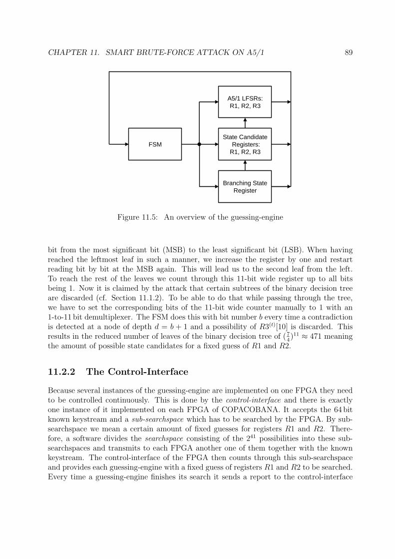
CHAPTER 11. SMART BRUTE-FORCE ATTACK ON A5/1 89
State CandidateRegisters:
R1, R2, R3FSM
A5/1 LFSRs:R1, R2, R3
Branching StateRegister
Figure 11.5: An overview of the guessing-engine
bit from the most significant bit (MSB) to the least significant bit (LSB). When havingreached the leftmost leaf in such a manner, we increase the register by one and restartreading bit by bit at the MSB again. This will lead us to the second leaf from the left.To reach the rest of the leaves we count through this 11-bit wide register up to all bitsbeing 1. Now it is claimed by the attack that certain subtrees of the binary decision treeare discarded (cf. Section 11.1.2). To be able to do that while passing through the tree,we have to set the corresponding bits of the 11-bit wide counter manually to 1 with an1-to-11 bit demultiplexer. The FSM does this with bit number b every time a contradictionis detected at a node of depth d = b + 1 and a possibility of R3(t)[10] is discarded. Thisresults in the reduced number of leaves of the binary decision tree of (7
4)11 ≈ 471 meaning
the amount of possible state candidates for a fixed guess of R1 and R2.
11.2.2 The Control-Interface
Because several instances of the guessing-engine are implemented on one FPGA they needto be controlled continuously. This is done by the control-interface and there is exactlyone instance of it implemented on each FPGA of COPACOBANA. It accepts the 64 bitknown keystream and a sub-searchspace which has to be searched by the FPGA. By sub-searchspace we mean a certain amount of fixed guesses for registers R1 and R2. There-fore, a software divides the searchspace consisting of the 241 possibilities into these sub-searchspaces and transmits to each FPGA another one of them together with the knownkeystream. The control-interface of the FPGA then counts through this sub-searchspaceand provides each guessing-engine with a fixed guess of registers R1 and R2 to be searched.Every time a guessing-engine finishes its search it sends a report to the control-interface

CHAPTER 11. SMART BRUTE-FORCE ATTACK ON A5/1 90
whether it was successful or not on finding a state candidate and requests for anotherfixed guess of registers R1 and R2 out of the current sub-searchspace. In case of suc-cess the valid state candidate is propagated to the software. This is repeated until thewhole sub-searchspace is searched by the FPGA. During the search, the software retrievesregularly at reasonable intervals the status information of each FPGA and assigns a newsub-searchspace to an FPGA if requested. The search is finished when all state candidatesthat can be generated with the 241 possibilities for guessing R1 and R2, i.e., the wholesearchspace, are checked for consistency.
11.2.3 Optimization: Storing Intermediate States
When completely passing through a binary decision tree, edges near the root node aretraversed much more often than edges near the leaf nodes. The number of cycles R3 needsto be clocked to reach any leaf of the tree is 11 (cf. Section 11.2.1). For example, wheninspecting the two leftmost leaves we have to go bit by bit through the states 00000000000and 00000000001 of the 11-bit wide counter corresponding to the tree. Apparently, thefirst ten edges up to the node of depth 10 for both leaves are identical. Therefore, we cancreate recovery points at some depth in the search tree. More precisely, it is possible tostore the intermediate state (i.e., the content of all A5/1 registers) at such a point (node oftree) and search the subtree starting at this recovery point instead of starting at the rootnode. This apparently demands a larger area, but saves a certain amount of clock-cycles.
Let us assume that reloading takes exactly one clock-cycle. If we store and reload theintermediate states at depth d = 10, then the number of clock-cycles for R3 reduces from11 to 11+1+1
2= 6.5 on average: 11 times clocking R3 to reach the first leaf, one clock-cycle
reloading the intermediate state, and one time clocking R3 to reach the next leaf fromthe reloaded state. If we store the intermediate states at depth d = 9, the correspondingsubtree has 4 leaves. To reach the leftmost one takes 11 clock-cycles, but to reach the other3 leaves will take just 1 + 2 = 3 clock-cycles each. Therefore, the average number of timesR3 needs to be clocked is in this case only 11+3+3+3
4= 8+3·4
4= 5.
Generalizing this approach of storing and reloading intermediate states at a depth of d = 10or d = 9 to a depth of d = b+ 1, where b denotes the number of the bit in the 11-bit widecounter consecutively numbered from 0 to 10, we need to clock R3
f(b) =b+ (11− b) · 2(10−b)
2(10−b) (11.1)
times on average to reach one leaf. The function has a minimum of 4.875 times clockingR3 on average to reach a leaf for storing and reloading intermediate states at a depth ofbmin = 7 for b ∈ N.
Taking also into account that some subtrees are discarded while passing through the tree(cf. Section 11.1.2) and the number of possibilities is reduced from 2 to 7
4for every guess,

CHAPTER 11. SMART BRUTE-FORCE ATTACK ON A5/1 91
f(b)g(b)
b0 2 4 6 8 10
4
5
6
7
8
9
10
11
Figure 11.6: Functions f(b), g(b): The average number of cycles clocking R3 to generate astate candidate with reloading intermediate states at recovery position b
the function needs to be adapted:
g(b) =b+ (11− b) · (7
4)(10−b)
(74)(10−b) . (11.2)
Both functions f(b) and g(b) are shown in Figure 11.6. The value for the minimum of thefunction g(b) now changes to approximately 5.31 at bmin = 7 for b ∈ N. Therefore, theexpected number of clock-cycles for generating and checking one state candidate is now
Topt = 1 +4
3· 5.31 + 2 ≈ 10.10 ≈ 23.33
instead of T = 1723
(cf. Section 11.1.2). This results in an optimized time complexity of
Copt ≈ 241 · 28.88 · 23.33 ≈ 253.21
and reduces the previous complexity of C ≈ 254.02 by 0.81 bit. But when comparing thetime complexities of the standard and the optimized guessing-engine we additionally haveto take the required area into account. The optimized guessing-engine is expected to occupya larger area because of the storing elements for intermediate states of several registers.Hence, we will be able to place less instances on one FPGA. This comparison of time-areaproducts is done after the implementation process and will be discussed in Section 11.3.

CHAPTER 11. SMART BRUTE-FORCE ATTACK ON A5/1 92
Table 11.1: Implementation results for the control-interface and the guessing-engines
slices flip-flops look-up tables fmax [MHz]
control-interface 371 304 254 123.19standard guessing-engine 202 179 256 112.84optimized guessing-engine 311 312 412 115.01
Table 11.2: Comparison of the implementation results of both guessing-engines
computing-time slices time-area product[clock-cycles] [clock-cycles · slices]
optimized 10.10 311 3,141.10standard 17.67 202 3,568.73optimizedstandard
0.57 1.54 0.88
11.3 Implementation Results for COPACOBANA
We used Xilinx ISE Foundation 9.2i to synthesize and implement all components for aXilinx Spartan3-XC3S1000-FT256 FPGA used in COPACOBANA. The simulation of thehardware model was done in MentorGraphics ModelSim SE 6.3d.
First, we implemented and tested one single instance of the standard and optimized guess-ing engine together with the control-interface for one instance. Therefore, Table 11.1shows the post place & route results of the implementation process for a single instance ofthe control-interface and both guessing-engines.
To decide whether it is worth or not implementing the optimized guessing-engine in spiteof the increased area consumption we calculated the time-area product. Table 11.2 shows acomparison of the computing time T and Topt in clock-cycles (cf. Sections 11.1.2 and 11.2.3),the number of slices needed, and the time-area product in clock-cycles·slices for our stan-dard and optimized implementation of the guessing-engine. The last row shows the quotientof the values of both designs. The quotient of the time-area products shows an overall im-provement of about 12% for one single optimized guessing-engine compared to the standardone. We omitted considering the operating frequencies in the time-area product becauseboth implementations run at nearly the same speed.
After having tested a single instance of each guessing-engine together with the control-interface on one of the Spartan3-XC3S1000 FPGAs we attempted to maximize the uti-lization ratio of the available hardware resources. For this purpose, we implemented asmany instances as possible of both types of guessing-engines with one instance of the

CHAPTER 11. SMART BRUTE-FORCE ATTACK ON A5/1 93
Table 11.3: Implementation results of the maximally utilized designs
slices FFs LUTs fmax [MHz] ftest [MHz]
1 control-engine &◦ 36 standard 6,953 ( 91 %) 10,730 10,576 81.85 72.00◦ 32 standard 6,614 ( 86 %) 9,636 9,417 102.42 92.00◦ 23 optimized 7,494 ( 98 %) 10,141 10,562 104.65 92.00guessing-enginesSpartan3-XC3S1000 7,680 (100 %) 15,360 15,360 300.00 —
control-interface. We were able to place & route 36 instances of the standard engine onone of the target FPGAs. However, the complexity of the control-interface grows with thenumber of guessing-engines. For 36 such engines the critical path was transfered to thecontrol-interface creating the bottle-neck of the design. Therefore, the achieved maximumfrequency of 81.13 MHz was relatively low. So we decided to implement less engines ata higher frequency instead. The best trade-off for the standard guessing-engine was toimplement 32 instances at a maximum frequency of 102.42 MHz. In case of the optimizedguessing-engine we were able to implement 23 instances running at 104.65 MHz. The im-plementation results of both complete designs are shown in Table 11.3. Additionally, theavailable resources of one FPGA are listed, too.
Table 11.3 also shows the frequencies the designs were tested with. Thus, we can calculatea preliminary estimation of the computation time to determine and check all possible statecandidates. For the slow design with the standard guessing-engine and a time complexityof C = 254.02 (cf. Section 11.1.2) we expect a computation time of
test =254.02
120 · 36 · 72 · 106· 1
3600h ≈ 16.31 h.
This is an estimation for a fully equipped COPACOBANA with 120 FPGAs. In accordanceto the previous calculation, the preliminary estimation of the computation time for thesmaller but faster standard design (32 instances @ 92 MHz) is t′est ≈ 14.36 h. For theoptimized guessing-engine (23 optimized instances @ 92 MHz) with a time complexity ofCopt = 253.21 we expect a computation time of t′′est ≈ 11.40 h.
Time measurements of several extended test runs on COPACOBANA showed an averagecomputation time of t′ = 13.58 h for the small and fast standard design to perform a com-plete search for a given 64 bit known keystream. Comparing this result to the estimationof the computing time t′est shows that the complexity differs only by 0.08 bit from ourmeasurements. The optimized design took an average computation time of t′′ = 11.78 hfor a full search. This equals a variation of only 0.05 bit between the estimated and themeasured computation time. Because these were the computation times for a full search

CHAPTER 11. SMART BRUTE-FORCE ATTACK ON A5/1 94
(i.e., the worst case) the expected average time for finding the valid state candidate is6.79 h for the standard design and 5.89 h for the optimized design, respectively.
11.4 Summary
In this Chapter we presented a guess-and-determine attack on the A5/1 stream cipher run-ning on the special-purpose hardware device COPACOBANA. It reveals the internal stateof the cipher in less than 6 hours on average demanding only 64 bits of known keystream.We like to stress that our attack is also very attractive with regard to financial costs whichis a significant factor for the practicability of an attack: The acquisition costs for COPA-COBANA are about 10,000 e. Since COPACOBANA has a maximum power consumptionof only 600 W, the attack also features very low operational costs. For instance, assuming10 cent per kWh the operational costs of an attack are only 36 cents.
We like to note that we just provided a machine efficiently solving the problem of recoveringa state of A5/1 after warm-up given 64 bits of known keystream. To break the GSMcommunication, the cipher needs to be tracked back to evaluate the internal state in whichthe cipher appeared just after loading the session key K. Albeit, this backtracking can bedone efficiently and in a fraction of time on almost any platform, as discussed in Chapter 14.
Further technical difficulties will certainly appear when it actually comes to eavesdroppingGSM calls. This is due to the frequency hopping method applied by GSM which makesit difficult to synchronize a receiver to the desired signal. Also the problem of obtainingknown plaintext is still under discussion in pertinent news groups and does not seem tobe fully solved. However, these are just some technical difficulties that certainly cannot beconsidered serious barriers for breaking GSM.

Chapter 12
Time-Memory Trade-off Attacks
The method of a time-memory trade-off (TMTO) attack was introduced by Martin Hellmanin 1980 [Hel80]. The goal of the method was to reduce the time necessary to break thecipher, which is particularly important if such an attack is repeated frequently. The attackis accelerated by certain data which are precomputed in advance and stored in tables(denoted as TMTO tables).
The method was originally invented for block ciphers, namely for DES. Since then some im-provements and modifications have been proposed. To save the number of memory accessesduring the attack, which become the bottleneck of the method, Rivest [D. 82] proposed amodification based on so-called distinguished points. Biryukov and Shamir [BS00] combinedthe Hellman’s method with an attack on stream ciphers developed by Babbage [Bab95] andGolic [Gol97]. The result of this combination is a time-memory-data trade-off (TMDTO)method, applicable particularly to stream ciphers. In 2003 Oechslin [Oec03] introducedso-called rainbow tables which are currently considered to be the most efficient variant forblock ciphers. However, this variant is inferior to the original Hellman’s approach in caseof multiple input data (which is the case of stream ciphers). Recently, Barkan, Biham andShamir [BBS06] presented a modification of rainbow tables, called the thin-rainbow tables.The thin-rainbow tables enable efficient implementation of the attack even in the case ofmultiple input data.
In the following text we bring an overview of the above mentioned methods. We followand extend the summary introduced in [Rup08]. We start from the description of theHellman’s approach targeted to block ciphers, followed by the description of the Rivest’svariant. Then we introduce Biryukov’s and Shamir’s idea of adopting the method to streamciphers and finally we conclude with the rainbow tables and thin-rainbow tables methods.The discussion on the method which was finally selected for an attack on A5/1 and wasimplemented in COPACOBANA is presented in Chapter 13.
95

CHAPTER 12. TIME-MEMORY TRADE-OFF ATTACKS 96
12.1 Original Hellman’s Approach
Let P ∈ P be the plaintext, k ∈ K be the key, and C ∈ C be the ciphertext. The encryptionfunction is a one-way function
E : P×K 7→ C. (12.1)
We denoteC = E(k, P ) = Ek(P ). (12.2)
A common problem in cryptanalysis is to invert the encryption function E, i.e. for the givenciphertext C, and known corresponding plaintext P , to find a key k, s.t. Equation 12.2holds.
LetN = |K| (12.3)
be the cardinality of the search space.
Brute-Force Attack. One approach to invert the encryption function is to perform thebrute-force attack, i.e. to encrypt the known plaintext P with all potential values of the keyk until the match between the result of encryption and the given ciphertext C is obtained.This approach is (repeatedly) applicable only for ciphers with relatively short key sizes,since it demands a long computation time T = N . For example, a brute force attack onDES (which has a key being 56 bits long) takes approx. one week on average when run onCOPACOBANA [KPP+06].
Table Look-Up. It is also possible to select certain plaintext P0 which is likely to appearin the encrypted data. Such a plaintext can be e.g. the header of a file with a certainformat, the sequence of spaces in the text files, etc. For a selected fixed plaintext P0 allpairs key-ciphertext {ki, Ci} are then precomputed and stored in the memory, sorted bythe ciphertext. When performing the actual attack, the ciphertext is looked up in thememory and the key is simply retrieved. The precomputation phase (the offline phase)demands a high computation power, but this phase is run just once. The attack itself (alsocalled the online phase) is then very fast, T = 1. However, this approach has an extremespace (memory) complexity, M = N . For example, in case of DES, the table would occupy256 × (64 + 64) bits, which is 260 bytes, or 220 TB.
12.1.1 Basic Idea
Hellman’s original idea [Hel80] was to make a compromise between the above two extremeapproaches. The cryptanalysis is again divided into two phases, the offline phase, and theonline phase. During the offline phase a huge amount of calculations is performed, butonly some results are stored in the memory (tape, disk, . . . ). This phase may last weeks,

CHAPTER 12. TIME-MEMORY TRADE-OFF ATTACKS 97
k0E→ C0
R→ k1E→ C1
R→ k2E→ C2
R→ k3 . . . kt−1E→ Ct−1
R→ kt
Figure 12.1: One chain in the Hellman TMTO
SP1 = k10f→ k11
f→ k12f→ · · · f→ k1,t−1
f→ k1,t = EP1
SP2 = k20f→ k21
f→ k22f→ · · · f→ k2,t−1
f→ k2,t = EP2
SP3 = k30f→ k31
f→ k32f→ · · · f→ k3,t−1
f→ k3,t = EP3...
SPm = km0f→ km1
f→ km2f→ · · · f→ km,t−1
f→ km,t = EPm
Figure 12.2: Time-memory trade-off table
months or even years. During the online phase, i.e. the actual attack, the encryptionfunction is inverted in a relatively short time with the help of the results precomputed andstored in the memory.
12.1.2 Offline Phase
In the offline phase, one tries to precompute (ideally all) pairs key-ciphertext {ki, Ci}. Toreduce memory requirements, the pairs are organized in chains — ciphertext Ci, which isthe product of the encryption P0 under the key ki, is used to generate the key ki+1 for thenext encryption, as shown in Figure 12.1. The encryption function E might be consideredas a pseudo-random function. Consequently, a pseudo-random walk in a key space K isperformed.
The key ki+1 is generated from the ciphertext Ci using so-called reduction and re-randomization function R. This function modifies Ci e.g. by permuting some bits (ifthe key and the ciphertext are of the same length) and/or omits some bits of Ci (if thekey is shorter than the ciphertext). The composition of an encryption function E and are-randomization function R forms so-called step function f :
f(k) = R(Ek(P0)). (12.4)
It also holds
ki+1 = f(ki). (12.5)
As a part of the precomputation phase, m unique keys k10, k20, . . . , km0 ∈ K are chosen.Those keys serve as start points SP1, SP2, . . . , SPm of chains as shown in Figure 12.2.Then, the step function f is t-times iteratively applied to each start point SPj, generatingt keys kji in each chain. The last generated element of each chain is called the end point

CHAPTER 12. TIME-MEMORY TRADE-OFF ATTACKS 98
EPj:
EPj = f t(SPj). (12.6)
The intermediate results are discarded and only the pairs {SPj, EPj} are stored, sorted bythe end points. With the knowledge of the start point and the end point, the whole chaincan be reconstructed later.
12.1.3 Online Phase
In the online phase, the cryptanalyst is given the ciphertext C0. The task is to find a keyK s.t.
C0 = EK(P0). (12.7)
To do so, first the re-randomization and reduction function R is applied to C0 and theresult
y1 = R(C0) = R(EK(P0)) = f(K) (12.8)
is compared to all end points. If a match is found, y1 = EPj, then either, according toEquation 12.5, the searched key is K = kj,t−1, or the end point EPj has multiple inverseimages (this case is called a false alarm). To restore the value of kj,t−1, the chain isrecomputed, i.e. the step function f is applied (t− 1)-times starting from SPj.
If no match is found or if a false alarm appears, then a new result
y2 = f(y1) = f(R(C0)) (12.9)
is calculated and compared to all end points again. If a match is found now, then the keykj,t−2 = f t−2(SPj) is recalculated and its validity is verified (e.g. by encrypting P0 withkj,t−2 and comparing the result with C0). This approach is iteratively applied, i.e. the newresults yi = f(yi−1) are successively calculated and compared to all end points until eithervalid match is found or until i ≥ t. If the match is found in the i-th step, yi = EPj, thenthe candidate for the key K is kj,t−i = f t−i(SPj).
12.1.4 Characteristics
In many real examples, the step function f is non-injective. This is caused either by non-injectivity of the re-randomization and reduction function R (e.g. in case of DES, the64-bit ciphertext is reduced to the 56-bit key) and/or by non-injectivity of the encryption

CHAPTER 12. TIME-MEMORY TRADE-OFF ATTACKS 99
function E itself (e.g. in case of A5/1 several distinct internal states can produce the samekeystream). The non-injectivity of f leads to multiple occurrences of some keys kji in thetable shown in Figure 12.2. However, even if the step function f were injective, then thereis still certain probability that some generated key kji matches a start point SP .
Multiple occurrences of some keys lead to chain merges and chain loops. The chain mergeappears if a duplicate key is generated in two distinct chains. From that moment on, bothchains continue with generating the same sequence of keys. The chain loop appears if somekey is generated twice in the same chain. Starting from the duplicate key, the chain repeatsthe sequence of already generated keys.
Both chain merges and chain loops cause reduced coverage of the key space K. Hellmanproved that it is not worth increasing the number of generated chains m, or the length ofchains t, beyond the point, where
mt2 = N, (12.10)
since the coverage does not increase too much then. Equation 12.10 is called the matrixstopping rule. Hellman recommends to set m = N
13 and t = N
13 . As the table contains
less than m · t = N23 keys, Hellman recommends to generate r = N
13 tables, each having
its unique re-randomization and reduction function R.
The following formulas are based on the analysis done in [Hel80].
Success Probability. The success probability of a single table was calculated by Hell-man to be
Ptable =1
N
m∑i=1
t−1∑j=0
(N − (i · t)
N
)j+1
. (12.11)
The success probability of r generated tables is approximated by
Ptotal = 1− (1− Ptable)r . (12.12)
Precomputation Time. This time is proportional to a total number of applications ofthe step function f . Therefore it is
PT = m · t · r. (12.13)
Memory Complexity. Only the start point and the end point are stored out of eachchain. If the start points were chosen to be e.g. consecutive numbers, then we need atleast bSP = dlog2(m)e bits to unambiguously identify each start point. To store information

CHAPTER 12. TIME-MEMORY TRADE-OFF ATTACKS 100
about the end point, we need bEP = dlog2(N)e bits. We generate r tables, each containingm chains, therefore the total memory complexity would be
M = r ·m · bpair, (12.14)
where bpair = bSP + bEP = dlog2(m)e+ dlog2(N)e.
Online Time. As described above, the search through a single table requires one appli-cation of R and up to t− 1 applications of f . If neglecting the time to handle false alarms,we get the worst case estimation for the search through r different tables as
T = r · t. (12.15)
Table Accesses. After each application of R or f , the result is looked up in the tables.Therefore the maximum number of table accesses is
TA = T = r · t. (12.16)
Parameters Choice. For recommended values of m = t = r = N13 , we obtain PT = N
applications of f in the precomputation phase, M = N23 pairs {SP,EP} to be stored, and
T = N23 applications of f followed by the same number TA = N
23 of table accesses in the
online phase.
12.2 Distinguished Points
An extreme number of table accesses TA in the online phase may jeopardize the attack.For example, in case of DES, the number of table accesses would be TA = N
23 = 237 1
3 .If we assume that one table access takes 1 ms on average (currently stated values of anaverage disk access time are about 8 ms), then we would need 5.5 years to finish up theonline phase.
To handle this problem, Rivest [D. 82] in 1982 proposed the modification of the originalHellman’s approach, based on so-called distinguished points. A distinguished point (DP)is a key with a certain property which is easy to verify, e.g. a key having the 20 mostsignificant bits being all zeros. The DP-property is usually characterized by a mask withthe length of d bits.

CHAPTER 12. TIME-MEMORY TRADE-OFF ATTACKS 101
12.2.1 Offline Phase
In the offline phase, each chain is generated until some distinguished point is reached.Therefore, the end point is always a distinguished point. Consequently, the chains do nothave constant length; the parameter t on a length of chain is replaced by the specificationof the DP-property, which usually states that DP is a point having d most significant bitsbeing zero. The DP-property is usually combined with the range [tmin, tmax] defining aminimum required and a maximum allowed length of the chain. The chains that do notreach the minimum required length tmin do not contribute significantly to the coverage ofthe table and hence such chains are discarded to save memory requirements. The chainsexceeding the maximum allowed length tmax are likely to run into the chain loop and forthis reason such chains are discarded as well. Only the chains having the length withinthe specified boundaries are stored. Out of each chain, the triple {SPj, EPj, lj} is stored,where lj is a length of the chain. However, the information on the length of chain can beomitted, as will be shown below.
Chain merges and loops. The detection of chain merges is very easy in this case. Iftwo chains merge, then both chains end up in the same distinguished point — the endpoint. As both chains contain the same sequence of keys from the point of merge, onlyone chain is stored to save memory requirements. Obviously, it is the longer chain whichis stored since it contributes to the coverage of the table more. Chain loops are preventedby setting the condition on the maximum allowed chain length tmax, as discussed above.
12.2.2 Online Phase
The online phase is similar to the online phase of the original Hellman’s method. First,the re-randomization and reduction function R is applied to the given ciphertext C0:
y1 = R(C0). (12.17)
Since all end points are DPs, then the result y1 is looked up in the table only when it is aDP. Otherwise, further results
yi = f(yi−1) (12.18)
are iteratively calculated until the DP is reached or until i ≥ tmax.
If the DP is reached but no match in the table is found, then the iterative calculationdescribed in Equation 12.18 is not continued, since there is no chance of any further match(each chain contains exactly one DP — the end point). Instead, the next table is processed.
If the DP is reached in the i-th step and the result yi matches to the end point EPj, thenthe candidate for the key K is retrieved as

CHAPTER 12. TIME-MEMORY TRADE-OFF ATTACKS 102
kj,lj−i = f lj−i(SPj), (12.19)
where lj is a length of the chain which has been stored in the triple {SPj, EPj, lj}.If the length of the chain has not been stored, then the step function f is iteratively appliedstarting from SPj
kj,` = f `(SPj), ` = 1, 2, . . . (12.20)
until kj,` ≡ y1. Then the candidate for the key K is the point kj,`−1.
12.2.3 Characteristics
The fact that chains do not have constant length, as well as the fact that some chains arediscarded due to the chain merges, lead to more complicated evaluation of the character-istics of the method. The following overview is based on the analysis made in [SRQL02].
Let m be the number of start points in one table, r be the number of tables, k be thebit-length of points in the table, d be the number of mask bits defining the DP-propertyand [tmin, tmax] be the minimum and maximum allowed length of chain.
The probability that a chain leads into a DP in less than l iterations of the step functionis
P1(l) = 1−l−1∏i=0
(1− 2k−d
2k − i
)≈ 1−
(1− 2k−d
2k − l−12
)l
. (12.21)
Since l� 2k , the probability P1(l) can be further approximated
P1(l) ≈ 1−(
1− 2k−d
2k
)l= 1−
(1− 1
2d
)l, (12.22)
however, this approximation is not used in [SRQL02].
Chain Length. The average chain length can be calculated as
lavg =
∑tmax
l=tminl × P (DP in exactly l iterations)∑tmax
l=tminP (DP in exactly l iterations)
. (12.23)
The denominator of Equation 12.23 represents the ratio between the number of chainshaving the length l ∈ [tmin, tmax] and the total number of chains. It is expressed as

CHAPTER 12. TIME-MEMORY TRADE-OFF ATTACKS 103
γ = P1(tmax)−P1(tmin−1) ≈(
1− 2k−d
2k − tmin−22
)tmin−1
−(
1− 2k−d
2k − tmax−12
)tmax
. (12.24)
Consequently, the number of chains having the length tmin ≤ l ≤ tmax is
m′ = m · γ ≈ m ·
((1− 2k−d
2k − tmin−22
)tmin−1
−(
1− 2k−d
2k − tmax−12
)tmax). (12.25)
As some chains are sorted out if chain merge appears, the final number m of chains in onetable is further reduced, m ≤ m′.
The average chain length is approximated as
lavg ≈((1− x)tmin−2 (tmin + 1−x
x
)− (1− x)tmax−1 (tmax + 1−x
x
))γ
, (12.26)
where
x =2k−d
2k − tmax+tmin
4
.
As some chains are sorted out if the chain merge appears, the actual average chain lengthl′avg differs from lavg. Since longer chains are more likely to merge than shorter chains, theactual average length l′avg is lower than lavg, as will be confirmed later in Section 13.3. Theactual average chain length l′avg is decreasing with growing m′ since chain merges are morefrequent.
Success Probability. The number of distinct keys covered by one table has been ap-proximated as
s(γm) ≈ N ·
(1−
(N
−lavgγm+ l2avgγm+N
) 1lavg−1
). (12.27)
Therefore the success probability of one table is
Ptable =s(γm)
N≈ 1−
(N
−lavgγm+ l2avgγm+N
) 1lavg−1
. (12.28)
Having r tables the total success probability can be approximated by
Ptotal ≈ 1− (1− Ptable)r . (12.29)

CHAPTER 12. TIME-MEMORY TRADE-OFF ATTACKS 104
Precomputation Time. The average number of the step functions applied to one chainduring the precomputation phase is
δ = tmax · (1− P1 (tmax)) + lavg · P1 (tmax) . (12.30)
As there are r ·m chains to be precomputed, the precomputation time is
PT = r ·m · δ (12.31)
PT ≈ r ·m ·
(tmax
(1− 2k−d
2k − tmax−12
)tmax
+ lavg
(1−
(1− 2k−d
2k − tmax−12
)tmax))(12.32)
step functions.
Memory complexity. Each table contains s(γm)l′avg
chains. To store information on chains
from r tables, we need
M =s(γm)
l′avg· r · btriple ≈
s(γm)
lavg· r · btriple (12.33)
bits of memory, where btriple = (dlog2(m)e) + (dlog2(N)e − d) + (dlog2(tmax)e) is the leastnumber of bits necessary to store information on one triple {SPj, EPj, lj}.
Online Time. The online time may be lower bounded by
T ≤ r · l′avg ≈ r · lavg. (12.34)
Table Accesses. The maximum number of table accesses may be bounded by a numberof tables
TA = r. (12.35)
since there is at most one look-up per one table.

CHAPTER 12. TIME-MEMORY TRADE-OFF ATTACKS 105
y0x0
y1x1
y2x2
y3x3
0100111101101010110100101010010100010010100010011110110001
y0x0
y1x1
y2x2
y3x3
y0x0 y0y0x0
y1x1 y1y1x1
y2x2 y2y2x2
y3x3 y3y3x3
0100111101101010110100101010010100010010100010011110110001
Figure 12.3: Sampling the keystream into D output prefixes
12.3 Time-Memory-Data Trade-off Attacks
The idea of a time-memory-data tradeoff attack, suitable for stream ciphers, was indepen-dently introduced by Babbage [Bab95] and Golic [Gol97]. Biryukov and Shamir [BS00]later combined this approach with the original Hellman’s method.
Let g be the function mapping each one of N internal states x ∈ X of the stream cipher tothe output prefix y ∈ Y. Output prefix y here is the string consisting of the first log2(N)bits produced by the cipher from this internal state
g : X 7→ Y. (12.36)
We denote
y = g(x). (12.37)
The typical cryptanalytical task in case of stream ciphers is to invert the function g, i.e.for the given output prefix y to find such x that Equation 12.37 holds.
Let w be the number of the available keystream bits. Since sometimes w > log2(N), it ispossible to derive D = w− log2(N) + 1 output prefixes y0, y1, · · · yD−1 from the keystream,as shown in Figure 12.3. To break the stream cipher, it is sufficient to find the internalstate xi for any of the D output prefixes yi. When the internal state xi is found, then thecipher can be run forward to derive the remainder of the keystream. In some cases, thecipher can also be run backwards, as shown in Chapter 14 for the case of A5/1.
The birthday paradox says that two subsets of the space withN points are likely to intersectif the product of their sizes exceeds N . The idea of Babbage and Golic was to apply thisproperty to the table look-up attack, which was described in Section 12.1. As we have Doutput prefixes available, then the size of the table is reduced to a fraction of ≈ N
Dpairs
{x, y}.The idea of Biryukov and Shamir was to apply this approach to the Hellman’s method.Consequently, the number of generated tables is D times smaller, rD = r
D, which saves
both the precomputation time

CHAPTER 12. TIME-MEMORY TRADE-OFF ATTACKS 106
PTD =PT
D(12.38)
and the memory
MD =M
D. (12.39)
The online complexity remains unchanged — for each data point we have to perform calcu-lations and table look-ups over the reduced number of tables rD, however these operationsare repeated for each of D data points. Therefore the online time is
TD = D · TD
= T (12.40)
and the number of table accesses is
TAD = D · TAD
= TA. (12.41)
12.4 Rainbow Tables
The idea of the rainbow tables, introduced in 2003 by Oechslin, is to apply a differentre-randomization and reduction function Ri in each step of chain generation. The methodwas first described for the use with block ciphers.
12.4.1 Offline Phase
The step function f changes from step to step creating the sequence of t different stepfunctions in each chain
f1f2f3 . . . ft (12.42)
Chain loops are completely prevented since each step function is used exactly once. Chainmerges are possible only if two identical data points are generated in the same column ofthe table, i.e. after application of the same step function fi in two distinct chains. Sincethe probability of chain merges is significantly reduced in comparison to the Hellman’sapproach, the number m of chains contained in one table can be increased to the value forwhich m · t ≈ N . Consequently, a single table or just a few tables are typically generatedin the precomputation phase.

CHAPTER 12. TIME-MEMORY TRADE-OFF ATTACKS 107
12.4.2 Online Phase
The online phase differs from the Hellman’s approach as there are different reductionfunctions used in each step of the chain generation. For a given ciphertext C0, first the resultRt(C0) is calculated and compared to all end points. If no match is found, then the resultft(Rt−1(C0)) is calculated and looked up in the table, then the result ft(ft−1(Rt−2(C0))),etc. If a match is found, then, similarly to the Hellman’s method, the corresponding chainis reconstructed to retrieve the candidate for the key.
12.4.3 Characteristics
The following results have been adopted from the analysis provided in [Oec03].
Success Probability. The success probability of one table has been estimated as
Ptable = 1−∏(
1− mi
N
), (12.43)
where m1 = m and mn+1 = N(1− e−mn
N
).
The success probability of r tables is, similarly to Hellman, estimated as
Ptotal = 1− (1− Ptable)r . (12.44)
Precomputation Time. The precomputation time is estimated in the same way likefor Hellman’s method
PT = m · t · r. (12.45)
Memory Complexity. Also the estimation of memory complexity is similar to Hell-man’s method
M = r ·m · bpair, (12.46)
where bpair = bSP + bEP = dlog2(m)e+ dlog2(N)e is the number of bits necessary to storeone pair {SP,EP}.
Online Time. In the i-th iteration of the online phase, 0 ≤ i ≤ t− 1, we first apply thefunction Rt−i, followed by i step functions ft−i+1, ft−i+2, · · · ft−1, ft. The maximum number

CHAPTER 12. TIME-MEMORY TRADE-OFF ATTACKS 108
of calculations for one table is then t(t+1)2
and the worst case time to search through r tablesis then
T = r · t(t+ 1)
2. (12.47)
However, as mentioned above, the number of tables r is typically a very small number.
Table Accesses. Each iteration of the online phase is finished with a table look-up.Therefore the maximum number of table accesses into one table is equal to t, and theworst case number of the accesses into r tables is
TA = r · t. (12.48)
Parameters Choice. For recommended values of m = N23 , t = N
13 and r = 1, we
obtain PT = N applications of f in the precomputation phase, M = N23 pairs {SP,EP}
to be stored, and T = N23
2calculations with TA = N
13 table accesses in the online phase.
12.5 Thin-Rainbow Tables
The rainbow tables method is inferior to the standard Hellman’s method, whenever mul-tiple data points are available, as has been shown in [BBS06]. Therefore, a pure rainbowmethod is not suitable for cryptanalysis of the stream ciphers.
The fact of having multiple data points enables to save precomputation time and mem-ory, similarly to the Hellman’s TMDTO described in Section 12.3. However, the onlinecomplexity is increased. The online time is
TD = D ·⌈ rD
⌉· t(t+ 1)
2(12.49)
and the number of table accesses is
TAD = D ·⌈ rD
⌉· t, (12.50)
where D is the number of data points. Since typically r < D (in many cases r = 1), thenthe product D ·
⌈rD
⌉> r, which indicates the increased online complexity.
To cope with this problem, Barkan, Biham and Shamir [BBS06] proposed a modifiedscheme called the thin-rainbow method. In this scheme, the shorter rainbow sequence con-sisting of S different step functions is t-times repeated during the generation of one chain,

CHAPTER 12. TIME-MEMORY TRADE-OFF ATTACKS 109
as shown below:
f1f2 . . . fSf1f2 . . . fS . . . . . . . . . f1f2 . . . fS. (12.51)
Each chain contains t rainbow sequences, each rainbow sequence consists of S different stepfunction. Consequently, each chain consists of tS + 1 points (including the start point andthe end point). By keeping t to be greater than D, t ≥ D, the optimum trade-off may bereached whenever the multiple data is available. If multiple tables are generated, then eachtable has its unique rainbow sequence f1f2 . . . fS. Let us note that by setting S = 1 weobtain the standard Hellman’s method (with multiple data) as described in Section 12.3.
12.5.1 Thin-Rainbow Tables with Distinguished Points
The method can be combined with the Rivest’s approach of the distinguished points toreduce the number of table accesses. In this case the DP-property is not checked after eachapplication of the step function, but only after each application of fS, which is the laststep function of each rainbow sequence. In the following text we focus on this variant.
12.5.2 Offline Phase
Similarly to previously described methods we generate m chains in each of r tables. Asthe distinguished points approach is applied, the chains do not have a constant length.Therefore, the definition of t is replaced by the definition of the DP-property being specifiedby a d-bit mask. We also set the region [tmin, tmax] of a minimum required and a maximumallowed length of the chain, which is here expressed in the number of rainbow sequences.Only the chains that reach the DP after tmin ≤ l ≤ tmax applications of a rainbow sequenceare stored in the table. If two chains merge (which is again detected by equal end point),then the shorter one is sorted out.
12.5.3 Online Phase
In the online phase we are given D data points y. Let’s focus on one data point yi, andone table. First, we calculate RS(yi) and check it for the DP-property. If a DP has beenreached, then we look-up the table. If not, then we follow with ` iterations of the rainbowsequence f1f2 . . . fS until DP is reached or until ` > tmax. In the second step we calculatefS(RS−1(yi)) first, check it for the DP-property and, if necessary, we continue the calcula-tion by ` rainbow sequences. In the next step, we start calculation with fS(fS−1(RS−2(yi))),etc. In the last step, we start the calculation with fS(fS−1 . . . f2(R1(yi)))), followed by `rainbow sequences, if necessary.
If the table has been completely processed/searched for the data point yi, and no success

CHAPTER 12. TIME-MEMORY TRADE-OFF ATTACKS 110
has been reached yet, then we follow the search with the same data point yi in the nexttable. After having processed the last table, the whole procedure is repeated for other datapoints y. If a match is found, then, similarly to the Hellman’s method, the correspondingchain is reconstructed to retrieve the candidate for the key/internal state.
12.5.4 Characteristics
The analysis of this method has been presented in [A.12]. This analysis is based on ap-proaches used in [SRQL02] and [Oec03]. The analysis in [A.12] is made for one table, herewe present the results for r tables. However, in many cases, r = 1.
Success Probability. To approximate the probability that the DP is reached in lessthan l applications of a rainbow sequence (or, in other words, in less then l applications offS), we use Equation 12.22
P1(l) ≈ 1−(
1− 1
2d
)l. (12.52)
The average length of a chain (in the number of rainbow sequences) is, from Equation 12.23,approximately
lavg ≈
∑tmax
l=tminl ×((
1− 12d
)l−1 −(1− 1
2d
)l)(1− 1
2d
)tmin−1 −(1− 1
2d
)tmax. (12.53)
The number of chains having the length tmin ≤ l ≤ tmax rainbow sequences (or, in otherwords, having the length tminS ≤ lS ≤ tmaxS step functions) is, similarly to Equa-tion 12.25, approximately
m′ ≈ m ·
((1− 1
2d
)tmin−1
−(
1− 1
2d
)tmax). (12.54)
As mentioned above, due to the chain merges the final number m of chains in one table islower, m ≤ m′, since the shorter ones of the merged chains are sorted out.
To evaluate the number of chains m, we used the iterative expression for mi, which repre-sents the number of distinct points in the i-th column of the table

CHAPTER 12. TIME-MEMORY TRADE-OFF ATTACKS 111
mi =
N − b iSc∑k=1
mi−kS
(1−(
1− 1
N
)mi−1)
≈
N − b iSc∑k=1
mi−kS
(1− emi−1
N
).
(12.55)
Upon setting m1 = m′ we obtain m = mlavgS+1.
Then the success probability of one table and one data point y is approximately
Ptable ≈mlavgS
N(12.56)
and the success probability of r tables and D data points y consequently is approximately
Ptotal ≈ 1−(
1− mlavgS
N
)rD. (12.57)
Precomputation time. Similarly to Equation 12.30 the average number of rainbowsequences applied to one chain is again equal to
δ = tmax · (1− P1 (tmax)) + lavg · P1 (tmax) . (12.58)
Since (i) each rainbow sequence is S step functions long, (ii) we (initially) generate m chainsin each table, and (iii) we generate r tables, then the precomputation time (expressed inthe number of step functions) can be approximated as
PT ≈ r ·m · δ · S. (12.59)
Memory Complexity. Each table contains m chains. To store information on the chainsfrom r tables we need
M = m · r · btriple (12.60)
bits of memory, where btriple = (dlog2(m)e) + (dlog2(N)e − d) + (dlog2(tmax)e) is the leastnumber of bits necessary to store information on one triple {SPj, EPj, lj}.

CHAPTER 12. TIME-MEMORY TRADE-OFF ATTACKS 112
Online Time. For one data point and one table we have to compute at most S chains,each being about S · δ step functions long. Therefore, for D data points and r tables, weobtain the worst case online complexity to be
T = r ·D · S · S · δ = r ·D · S2 · δ. (12.61)
Table Accesses. Calculation of each chain is finished by one table look-up (if the DP isreached before tmax iterations of the rainbow sequence). Therefore, the worst case numberof the table accesses is
TA = r ·D · S. (12.62)
Parameters Choice. Let assume that only one table is generated, r = 1. We set sucha DP-criterion and the region [tmin, tmax] to obtain lavg ≈ D. If P1(tmax) > 0.5, then,according to Equation 12.58, we may roughly approximate δ ≈ lavg ≈ D. The length of
one rainbow sequence we set as S ≈ N13
D. The number of chains to be precomputed is set
as m ≈ N23
D.
After the substitution to Equations 12.57–12.62, we obtain a success probability Ptotal ≈1 −
(1− 1
D
)D ≈ 1 − 1e, precomputation time PT ≈ N
D, memory complexity M < N
23
D
triples {SP,EP, l}, online time T ≈ N23 and the number of table accesses TA ≈ N
13 .
As obvious from these very rough estimations, on careful selection of the parameters, thecharacteristics of the thin-rainbow DP TMDTO method are comparable to the Hellman’sDP TMDTO method, discussed in Sections 12.2 and 12.3.

Chapter 13
Time-Memory-Data Trade-off Attackon A5/1
In this chapter we describe our implementation of TMDTO attack on A5/1. COPA-COBANA is used to perform calculations in both the precomputation and the onlinephase.
In the first part we focus on the precomputation phase. Upon analysis made in Chap-ter 12 we make a selection of the method to be implemented in COPACOBANA. Afterthat we analyze potential design approaches for hardware architecture and we select theapproach that permits achievement of maximum performance. Then the description ofthe architecture for the table precomputation follows. We continue with a description ofa method for the fast sort of disk-stored TMTO tables. The first part we conclude withimplementation results which we obtained after the test run of the precomputation phase.We compare theoretical and practical results and we identify some of potential sourcesmaking differences between them.
In the second part we focus on the online phase. We describe the architecture of theonline engine which has been implemented in COPACOBANA. The online engine is morecomplex than the precomputation one. After that, we discuss the method used for the fastlook-up in disk-stored TMDTO table.
This has been a collaborative work with Andy Rupp. Some results of this work havealready been published in [A.12].
13.1 Table Precomputation
To make our attack realistic, we assume that the number of known consecutive keystreambits is relatively small, but still we consider that we know at least one whole keystreamblock of 114 bits. Hence, we have D = 114 − 64 + 1 = 51 data points available to break
113

CHAPTER 13. TIME-MEMORY-DATA TRADE-OFF ATTACK ON A5/1 114
the cipher.
13.1.1 Chosen Method
Both Hellman’s original tradeoff and rainbow tables are well suited for parallelization inhardware. Since the chains have a fixed length, the control of the calculation in theprecomputation phase is simple. However, as discussed above, the Hellman’s methodrequires a large number of disk accesses during the online phase, and the rainbow tabletradeoff curve is inferior to Hellman’s one whenever we have multiple data [BBS06].
Ergo, we considered two candidates for the implementation: the Hellman’s DP TMDTOmethod, described in Sections 12.2 and 12.3, and the thin-rainbow DP TMDTO methoddescribed in Section 12.5. Both methods provide comparable characteristics with regardto success probability Ptotal, precomputation time PT , memory complexity M , online timeT , as well as a low number of table accesses TA. Nevertheless, there is a certain importantdifference in both methods: in case of the Hellman’s DP method, the chain can reach itsend point after any application of the step function f , while in case of the thin-rainbow DPmethod, the chain can reach its end point only after application of the last step functionof the rainbow sequence, fS. In other words, in case of the Hellman’s DP we have to testthe DP-property after each application of f , while in case of the thin-rainbow DP, we haveto test it after fS only. By exploiting this property we may save considerable amountof hardware resources necessary for the units testing the DP-property, and therefore wemay gain higher performance. Hence, for our implementation, we have selected the thin-rainbow DP method. In the case of multiple data this approach allows simple and efficienthardware implementation, while exhibiting a low number of disk accesses during the onlinephase.
13.1.2 Design Approach
Most designs realized in FPGAs usually do not fully use flip-flops available on the chip.Typically, the designs are limited by the number of combinational resources (look-up tables,LUTs) available. In case of A5/1 it is different: a demand for flip-flops prevails a demandfor combinational logic.
As generally known, the best performance may be gained by exploiting the propertiesof a target architecture. Let’s focus on it now. Xilinx Spartan 3-1000 FPGA used inCOPACOBANA contains 7680 slices [Xil07]. Each slice contains 2 LUTs and 2 flip-flops(and other circuits, like the fast carry logic or dedicated multiplexers), see Figure 13.1.Look-up tables are used to implement combinational logic, but in some slices the LUTscan also be configured to work as a shift register with a maximum length of 16 bits (denotedas SRL16). This property enables to implement much bigger shift-register-based circuits.For example, using all 15360 flip-flops we may build the circuit containing equivalent of15360/64 = 240 A5/1 cores (without any controller and other circuits). On the other

CHAPTER 13. TIME-MEMORY-DATA TRADE-OFF ATTACK ON A5/1 115
Look-upTable
Flip-flop
Look-upTable
Flip-flop
Figure 13.1: Simplified diagram of Xilinx FPGA slice
hand, using SRL16s we can implement up to 480 A5/1 cores, still leaving enough LUTsand flip-flops for a controller and other necessary circuits.
However, the usage of SRL16s brings some limitations to the circuit design. To allow thesynthesis tool to utilize this property, we have to avoid any parallel input or output to theshift register, using only serial input and output. Hence we rejected the idea of building thepipeline as at the DES engine [KPP+06], since such a pipeline would require parallel accessto all bits of registers in each pipeline stage. Instead, we decided to implement an array ofsmall, encapsulated, independent processing units (we call them TMTO elements), eachhaving one serial input and one serial output.
13.1.3 The TMTO Element
The diagram of the TMTO element is shown in Figure 13.2. The element consists of twomodified A5/1 cores, which can be operated either in RUN mode, or in LOAD mode. InRUN mode the Core operates as a standard A5/1 unit, i.e. it produces the keystream.When switched to LOAD mode, the registers R1, R2 and R3 are interconnected to createone large 64-bit shift register with one serial input and one serial output.
Each TMTO element is calculating one chain of points, i.e. one row in the TMTO table. Itworks like a two-stroke two-piston engine. In odd steps of the rainbow sequence, the Core#1 produces the keystream yj,i that is on-the-fly re-randomized and loaded to the Core #2as the new internal state xj,i+1. In even steps of the rainbow sequence, the functionalitiesof both cores are swapped — now the Core #2 is in RUN mode, while the Core #1 isin LOAD mode. When the rainbow sequence is finished (i.e. after application of fS), theresult stored in the Core #1 is shifted out to be checked for the DP-property. As obvious,

CHAPTER 13. TIME-MEMORY-DATA TRADE-OFF ATTACK ON A5/1 116
XOR
A5/1 core #1
A5/1 core #2 XOR
load
load/run_2
load/run_1
re-randomization function
Figure 13.2: TMTO element — a processing unit calculating one chain of the table
our design requires the rainbow sequence to be even number of steps long (S must be aneven number), however, this fact does not represent any significant limitation.
As a source of re-randomization, we use the output of the long-period LFSR. The outputof LFSR is XORed with the keystream.
13.1.4 Architecture of the Table Precomputation Engine
An architecture of the precomputation engine, occupying one FPGA, is presented in Fig-ure 13.3. Since COPACOBANA hosts up to 120 FPGA, we may place the same numberof precomputation engines in one COPACOBANA.
We were able to place 234 TMTO elements into one FPGA. The TMTO elements aredepicted in the upper part of the diagram. To gain the maximum frequency, we rejectedthe idea of parallel access to the TMTO elements, since the number of them is relativelylarge. Instead, we connected all TMTO elements into one large chain. The communicationoverhead, increased due to the serial access, still represents only a small fraction of theoverall computation time, which is more than compensated by the increased frequency.
All TMTO elements share one DP checker depicted on the left side of the diagram. Afterthe application of fS, the results held in TMTO elements are shifted out to be checked forthe DP-property by this unit.
The 64-bit start point generator consists of a 40-bit register holding the static value of upperbits, and a 24-bit counter generating the value of lower bits. By incrementation, the countergenerates the sequence of consecutive start points. Upon startup of COPACOBANA thestart point generator is initialized with a certain initial value; each precomputation engine(i.e. each FPGA) is assigned its unique initial value by the host computer. Besides that,each precomputation engine is also assigned the range of the start point values to begenerated. When this range is exhausted, the host computer assigns a new range — anda new initial value of the start point generator — to the precomputation engine, and theengine is reset.

CHAPTER 13. TIME-MEMORY-DATA TRADE-OFF ATTACK ON A5/1 117
XOR
A5/1 core #1
A5/1 core #2 XOR
load
load/run_2
load/run_1
re-randomization function
TMTO element
TMTO element
TMTO element
point register
start point generator
CONTROLLER
re-randomization function
generator
chain memory(start point,birthdate)
FIFO
DPchecker
timerC
ON
TR
OL
& E
VA
LUA
TIO
NE
XE
CU
TIO
N
Figure 13.3: Architecture of an A5/1 precomputation engine

CHAPTER 13. TIME-MEMORY-DATA TRADE-OFF ATTACK ON A5/1 118
The point register is a 64-bit shift register with a parallel load. Newly generated startpoint is loaded from the start point generator to the point register, from which it is thenshifted out to the corresponding TMTO element.
The timer is incremented at the beginning of each rainbow sequence. It is used to determinethe length of each generated chain, as discussed below.
For each chain, generated in the specific TMTO element, a value of its start point and its‘birthdate’ is stored in the chain memory. The ‘birthdate’ is a value of the timer at timeof start point generation.
As discussed above, we use the long-period LFSR as a re-randomization function generator.This unit is again shared by all TMTO elements, since all TMTO elements use the samere-randomization function Ri at the same time.
The information on the start point, the end point and the length of each successfullygenerated chain is collected in a FIFO, from which it is read in bursts by the host computer.
How It Works. After the reset, the controller runs the initialization phase, duringwhich all TMTO elements are initialized with start points. This phase is run exactly once.After that, during a standard operation, phases of execution are alternated with phases ofevaluation.
Initialization. During initialization the TMTO elements are switched to build, togetherwith point register, one large shift register. Start points generated for all TMTO elementare loaded to the point register and shifted to the corresponding TMTO elements. The val-ues of start points and their ‘birthdates’ (time of their generation) are concurrently storedin the chain memory. Besides that the timer, the re-randomization function generator andsome other auxiliary circuits are initialized.
Execution. Execution itself is performed in TMTO elements. One phase of executionlasts exactly one rainbow sequence. The function has been already described in Subsec-tion 13.1.3.
Evaluation. When the rainbow sequence is finished, all TMTO elements are againswitched into one large shift register and the results are shifted-out. The results are on-the-fly checked for the DP-property, and the length l of each chain is calculated as a differencebetween a ‘current date’ (which is the current value of the timer) and the ‘birthdate’ ofthe corresponding chain, which is stored in the chain memory. For each chain one of thefollowing four cases may appear:
1. If the result satisfies the DP-property (it is the end point) and if the length l of thechain is within bounds, tmin ≤ l ≤ tmax, then the chain information (start point, end

CHAPTER 13. TIME-MEMORY-DATA TRADE-OFF ATTACK ON A5/1 119
point, length) is stored into FIFO — the value of the end point is acquired from thepoint register and the value of the start point is acquired from the chain memory.
Concurrently, a new start point is generated, as a new chain will be calculated in thecorresponding TMTO element. This new start point replaces the end point in thepoint register. At the same moment, both the new start point and the ‘birthdate’are stored in the chain memory.
Information stored in FIFO is later read out by the host computer and stored on thedisk.
2. If the end point has been achieved, but the chain is too short, l < tmin, then thechain is discarded and the generation of a new chain is initiated in the same TMTOelement — the procedure is the same as above (the new start point is generated,loaded into the point register and, together with a ‘birthdate’, stored in the chainmemory), but the chain information is not stored in FIFO.
3. If the chain becomes too large, l > tmax, then again the chain is discarded and thegeneration of a new chain is initiated in the same TMTO element.
4. In all other cases (i.e. the end point has not been achieved and the chain is not toolong yet) the result is simply shifted back to the TMTO element to continue withthe next rainbow sequence.
During the phase of evaluation we also initialize the re-randomization function generatorto generate the same rainbow sequence in the next phase of execution.
13.1.5 Data Transfer from COPACOBANA to the Host Com-puter
The host computer regularly polls every FPGA, reads out the chains information collectedin FIFO, and stores it on the disk. As evident from the diagram of COPACOBANA(see Figure 10.3), the data is transfered via the bus and the interface. For its electricalproperties the bus represents relatively high risk of data corruption.
As clear from the previous discussions, all stored data must be correct, otherwise they maylead to incorrect results during the online phase of the attack. On the other hand, lost ofany chain information does not represent any significant problem — a new chain may becalculated instead.
We have chosen a Hamming code to secure the correctness of the transfered data. The64-bit start points and end points are encoded with the Hamming code(72, 64) and thelength l is encoded with the Hamming code(16, 11). Though these codes are commonlyused as SEC-DED (single error correction, double error detection) codes, we use them asTED (triple error detection) code for further improvement in the error resistance. If an

CHAPTER 13. TIME-MEMORY-DATA TRADE-OFF ATTACK ON A5/1 120
Table 13.1: A5/1 TMDTO: Expected runtimes and memory requirements
# m S d Il PT M T TA Ptotal[days] [TB] [secs]
1 241 215 5 [23,26] 337.5 7.49 70.5 221 0.862 239 215 5 [23,27] 95.4 3.25 92.0 221 0.673 240 214 5 [24,27] 95.4 4.85 27.6 220 0.634 240 214 5 [23,26] 84.4 7.04 17.7 220 0.605 239 215 5 [23,26] 84.4 3.48 70.5 221 0.606 240 214 5 [24,26] 84.4 5.06 21.5 220 0.557 237 215 6 [24,28] 47.7 0.79 186.3 221 0.428 236 216 6 [24,28] 47.7 0.39 745.3 222 0.42
error appears, then the chain information is simply discarded. Besides the detection of100% of single, double and triple errors, the variant of the Hamming code(72, 64) usedensures also the detection of 99.19% of all quadruple errors [Hsi70].
13.1.6 Selection of Parameters
The A5/1 table precomputation engine can run at a maximum frequency of 156 MHz.Computing the step-function fi takes 64 clock cycles. One FPGA contains 234 TMTO el-ements (each consisting of two A5/1 cores), hence the whole COPACOBANA can performapproximately 236 step-functions per second. In contrast to that, a contemporary PC canexecute just about 222 step-functions per second [BBK06]. The performance of COPA-COBANA in the online phase is about 234.65 step-functions per second, see Section 13.4.
To select the TMDTO parameters (like the length S of the rainbow sequence, the numberd of bits defining the DP-criterion, the interval Il = [tmin, tmax] defining the minimum andmaximum number of rainbow sequence applications as well as the number m of start points)requires special attention, since this highly influences the precomputation time (PT ), thedisk usage (M), as well as the time needed in the online phase for the chain computations(T ), the number of table accesses (TA) and the success rate (Ptotal). Table 13.1 summarizesthe results for different sets of parameter choices. In all cases we consider generation of justone table (r = 1). The estimations are based on the analysis presented in Subsection 12.5.4under the assumption that D = 64. Furthermore, we assumed that COPACOBANA isused also for the online phase. Due to this, it is worth trading higher online complexity,e.g., for lower demand for disk space (compare rows 4 and 5).
For our implementation, we have selected the set of parameters presented in the third row,since it produces a reasonable precomputation time and a reasonable size of the tables, aswell as a relatively small number of table accesses. The success rate of 63% may seem tobe small, but it increases significantly if more data samples are available: For instance, if

CHAPTER 13. TIME-MEMORY-DATA TRADE-OFF ATTACK ON A5/1 121
…0…
…1…
…2…
…F…
...
Partially sorted table
FilesBuffers
...
…0…
…1…
…2…
…F…
Figure 13.4: Memory buffers minimize the fragmentation of files in RadixSort
four frames of known keystream are available, then D = 4 · 51 = 204 and thus the successrate is increased to 96%.
13.2 Fast Sort of Disk Stored TMTO Tables
The generated TMDTO table has to be sorted according to the end points. The averagedisk access time disables implementation of any “random access” sorting algorithm likeQuickSort, HeapSort etc. on the TMDTO table stored on the disk. For example, letassume that we will sort 4.85 TB of data, representing about 238.5 triples {SP,EP, l} (row3 in Table 13.1). To sort m = 238.5 data records, we need to perform about m× log2(m) =238.5 × 38.5 ≈ 243.8 data comparisons and transfers. If we assume that the average accesstime is just 1 ms (currently stated values of the average access time are about 8 ms), thenwe would need about 233.8 seconds (more than 450 years) to sort the table.
Standard RadixSort [Knu98], sometimes also denoted as LSD (least significant digit) Radix-Sort, is more suitable in this case. Let R denotes the value of radix used in the algorithm.Sorting in RadixSort consists of several passes (iterations) during which all data is trans-fered from one disk to other disk. In each pass, the transfered data is distributed amongR files in the target disk; each file contains all data sharing the same value of the digit incurrently inspected order of their keys. The number of passes k = dlogR(N)e depends onthe range N of values used as a key in the algorithm, and the radix R.
To minimize fragmentation of target files, which minimizes the number of disk seeks, it isworth implementing a set of buffers in a computer RAM, as shown in Figure 13.4. Thesorted data is distributed among the buffers; when a buffer is full, then the whole contents

CHAPTER 13. TIME-MEMORY-DATA TRADE-OFF ATTACK ON A5/1 122
of the buffer is at once transfered to the disk and the buffer is emptied. The performanceof RadixSort is then limited by the disk data transfer rate, which is stated to be aboutfB = 100 MB/s at maximum (however, we measured the transfer rate of about 50 MB/sonly).
Example 13.1. Let’s focus on the set of parameters presented in the third row ofTable 13.1. One pass, i.e one transfer of overall data, lasts at least Tpass = M
fB=
4.85 TB100 MB/s = 48500 seconds ≈ 13.5 hours in this case. However, in reality, this timewould be at least four times longer (≈ 54 hours). It is for two reasons: (i) the realtransfer rate is just 50 MB/s and (ii) reading from the source disk and writing tothe target disk are not performed concurrently. At any time, we either read the datafrom the source disk and sort them among memory buffers, or we empty a memorybuffer to the target disk. Concurrent reading and writing is also feasible, however, itdemands for sophisticated control.
Since we use end points as the keys for the sorting algorithm, then N = 264−d =264−5 in our case, where d is the number of bits defining the DP-property. If wechoose R = 16, then the number of passes is k = 15, and a complete sort of thetable will last at least Tsort = k × Tpass = 15 × 48500 = 727500 seconds ≈ 8.4 days.However, as discussed above, we expect this time to be at least four times longer, i.e.Tsort ≈ 33.7 days. If we choose R = 256, then k = 8 and the sort time is at least 4.5days (or 18 days).
We would like to stress that the value of radix R should be carefully chosen. Too smallvalue of R leads to enormous number of passes k. On the other hand, too big value of Rincreases fragmentation of target files (hence the number of disk seeks), since the memorybuffers are too small in this case.
13.2.1 Implemented Method
The speed of RadixSort algorithm is limited by the disk data transfer rate. Hence theminimization of the data volume to be transfered from/to disk represents the way toaccelerate the sorting of the data stored on the disk. In our implementation we havedecided to use the combination of MSD (most significant digit) RadixSort and any “RAM-efficient” standard sorting algorithm. This enables sorting the table in k passes, wherek = 3 for typical sizes M of TMDTO tables (between 1 TB and 10 TB) and typicalinstalled capacities of RAM (at least 1 GB).
In the first k− 1 passes, we split the data records from the unsorted TMDTO table into nfiles according to the most significant digits of end points, as shown in Figure 13.5. In thefirst pass we split the unsorted table into R1 ≈ k−1
√n files according to the most significant
digit of end points, in the second pass we split each of R1 files into R2 ≈ k−1√n smaller
files according to the second most significant digit, etc. To minimize fragmentation of thetarget files we again use memory buffers shown in Figure 13.4. Since the values of end
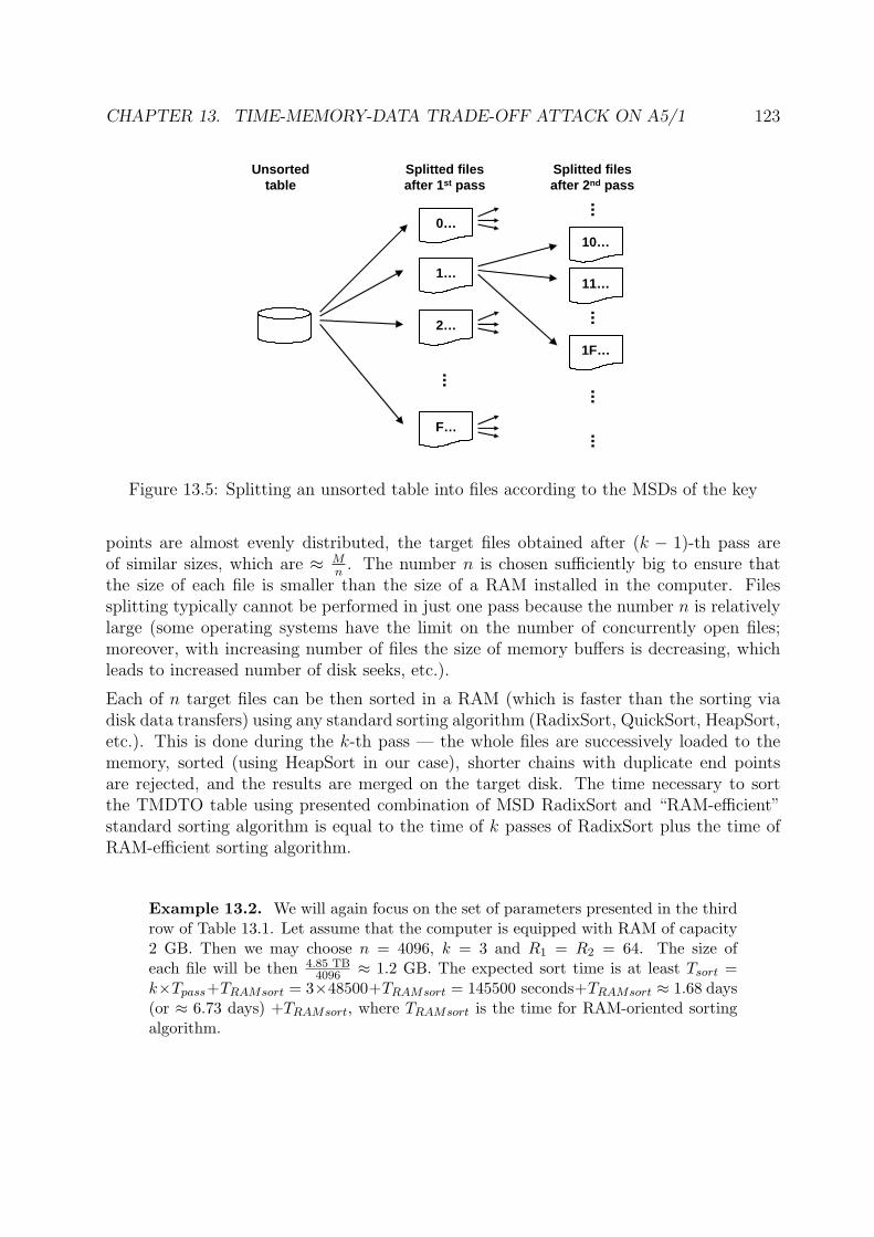
CHAPTER 13. TIME-MEMORY-DATA TRADE-OFF ATTACK ON A5/1 123
0…
1…
2…
F…
10…
11…
1F…
...
......
......
Unsorted table
Splitted files after 1 st pass
Splitted files after 2 nd pass
Figure 13.5: Splitting an unsorted table into files according to the MSDs of the key
points are almost evenly distributed, the target files obtained after (k − 1)-th pass areof similar sizes, which are ≈ M
n. The number n is chosen sufficiently big to ensure that
the size of each file is smaller than the size of a RAM installed in the computer. Filessplitting typically cannot be performed in just one pass because the number n is relativelylarge (some operating systems have the limit on the number of concurrently open files;moreover, with increasing number of files the size of memory buffers is decreasing, whichleads to increased number of disk seeks, etc.).
Each of n target files can be then sorted in a RAM (which is faster than the sorting viadisk data transfers) using any standard sorting algorithm (RadixSort, QuickSort, HeapSort,etc.). This is done during the k-th pass — the whole files are successively loaded to thememory, sorted (using HeapSort in our case), shorter chains with duplicate end pointsare rejected, and the results are merged on the target disk. The time necessary to sortthe TMDTO table using presented combination of MSD RadixSort and “RAM-efficient”standard sorting algorithm is equal to the time of k passes of RadixSort plus the time ofRAM-efficient sorting algorithm.
Example 13.2. We will again focus on the set of parameters presented in the thirdrow of Table 13.1. Let assume that the computer is equipped with RAM of capacity2 GB. Then we may choose n = 4096, k = 3 and R1 = R2 = 64. The size ofeach file will be then 4.85 TB
4096 ≈ 1.2 GB. The expected sort time is at least Tsort =k×Tpass+TRAMsort = 3×48500+TRAMsort = 145500 seconds+TRAMsort ≈ 1.68 days(or ≈ 6.73 days) +TRAMsort, where TRAMsort is the time for RAM-oriented sortingalgorithm.

CHAPTER 13. TIME-MEMORY-DATA TRADE-OFF ATTACK ON A5/1 124
13.3 Implementation Results — the Precomputation
Phase
As mentioned in Subsection 13.1.5, chain information is encoded with the Hamming codebefore transportation over the COPA bus (which has 64 data lines). Moreover, somestatus information is added, too. Therefore, the information on triple {SP,EP, l} of eachsuccessfully generated chain is transfered in three 64-bit words (192 bits).
For the set of parameters presented in the third row of Table 13.1, we obtain the followingresults: The number of chains having the lengths between 24 and 27 rainbow sequences ism′ ≈ 239.27. The precomputation time is Tpr ≈ 222.97 seconds, therefore, COPA generatesabout 216.30 chains per second on average, which represents the data rate of 216.30 × 192 ≈15.5 Mbits/s.
To connect COPACOBANA with a host computer, two versions of an interface have beendeveloped: the USB interface and the 1 Gbit/s Ethernet one. Unfortunately, for some tech-nical problems, none of them provides sufficient data throughput; the maximum measureddata rate of the USB interface is about 10 kbits/s, and the maximum measured data rateof the Ethernet interface is about 300 kbits/s. Since the technical problems do not seemto be solvable (the problems are likely caused by a third-party hardware and/or softwaremodules), a new interface is currently under development.
To partially compensate limited throughput of the interface, we have decided to use a setof parameters presented in the eighth row of Table 13.1 for our initial implementation.A prolonged rainbow sequence (S = 216) and a higher value of d ensure the generationof longer chains, which in turn represents lower demand for transfered data. Concretely,during Tpr ≈ 221.97 seconds COPA generates m′ ≈ 235.63 chains having the length between
24 and 28 rainbow sequences, which represents the demand for the data rate of 235.63
221.97×192 ≈2.5 Mbits/s. This is still well beyond the possibilities of the interface, however, the ratiobetween captured data and all generated data increases from about 2 % to about 12 %.On the other hand, for this improvement we pay by an increased number of table accessesin the online phase.
We used two COPACOBANAs, COPA1 and COPA2, for table precomputation. Bothmachines were running for a couple of months. During this time we have successfullycollected 14117445263 ≈ 233.717 chains generated by COPA1 and 11772717296 ≈ 233.455
chains generated by COPA2 (altogether 25890162559 ≈ 234.592 chains). The chains weresorted according to their end points, and in cases of duplicate end points, the shorter chainswere sorted out. We would like to stress that all chains acquired from COPACOBANAshave their length in the range of [24, 28] rainbow sequences; hence the number of themcorresponds to number m′. Chains having their length out of this range are discardedinside COPACOBANAs. Let us note that it is impossible to verify the correctness ofEquation 12.54, as many chains were lost due to the slow communication interface. Con-cretely, according to Equation 12.54, the number of chains generated in COPA2 will be

CHAPTER 13. TIME-MEMORY-DATA TRADE-OFF ATTACK ON A5/1 125
m ≈ 11772717296/0.772 ≈ 15252470254 ≈ 233.828 chains. However, during its running timeCOPA2 generated m = 107305012412 ≈ 236.643 chains, which is about 7 times more.
An average chain length calculated by Equation 12.53 is lavg ≈ 73.459 rainbow sequences.An average length of chains acquired from COPA2 was lavg = 73.389 rainbow sequences— it differs from the theoretical value by ≈ 0.1%. Unfortunately, we have not measuredthis length in the set of chains acquired from COPA1.
As discussed in Section 12.2, the average chain length l′avg decreases after rejection of chainswith duplicate end points. To investigate the dependency of l′avg on the number m of chainswith unique end points, and also to investigate the dependency of m on the number ofgenerated chains m′, we split the data generated by COPA2 into 10 sets 0, 1, . . . 9 ofvolumes 225, 225, 226, 227, 228, 229, 230, 231, 232 and 231.568 chains. Each set was separatelysorted, the shorter chains with duplicate end points were rejected, and both the numberof chains m and their average length l′avg were measured. Then the sets were successivelymerged, until all sets were united. After each merge shorter chains with duplicate endpoints were again rejected and the values m and l′avg were measured. Since some unions ofsets have the same volumes m′ as some single sets (e.g. the union of sets 0 and 1 has thesame volume as the set 2), we obtain multiple measurements for some volumes m′. Finally,we added the set generated by COPA1.
All results are summarized in Table 13.2. As visible from Table 13.2 and from Figure 13.6,the average chain length l′avg is decreasing with growing m, as has been discussed in Sub-section 12.2.3.
Table 13.2 brings also theoretical values of m, calculated by iterative Equation 12.55. Asevident from Table 13.2, as well as from the chart in Figure 13.7, the real measured valuesof m are smaller than the theoretical ones. This is mainly caused by the difference ofassumptions under which Equation 12.55 has been derived, and a real behavior of the stepfunctions f together with the real operating conditions.
Equation 12.55 is based on the assumption that the step function fi has probabilisticbehavior, i.e. every data point can be produced with the same probability. However, thisdoes not conform to the real behavior of the step function composed from the encryptionfunction g of the A5/1 cipher and the re-randomization function Ri. The main problemlies in the non-injective and non-surjective behavior of the A5/1 cipher [Gol97] (see alsoChapter 14), which reduces the set of points generated by the step function fi.
We also considered all start points to be randomly chosen, or, more precisely, we con-sidered the choice of start points not to be influencing the number m. However, in ourimplementation, the start points are generated as a sequence of consecutive values. Thisfact, together with the non-injectivity of A5/1 cipher, causes (at least) 1
8of generated
chains to be merging another chain after the first step function, as shown below. Otherchain merges occur due to other reasons.

CHAPTER 13. TIME-MEMORY-DATA TRADE-OFF ATTACK ON A5/1 126
Table 13.2: Theoretical and measured values of the number of chains in the table (m)and their average length (l′avg) after rejection of chains with duplicate end points. Valuespresented here are for different volumes of sets m′ (sets with chains having their length inrange [24, 28] rainbow sequences).
Measured values Theoretical values
sets m′ l′avg m mm′
m mm′
COPA2
0 225 73.383 224.828 0.887 225 11 225 73.424 224.836 0.893 225 10–1 226 73.399 225.829 0.888 226 12 226 73.408 225.878 0.919 226 13 227 73.39 226.939 0.959 227 12–3 227.585 73.382 227.502 0.944 227.582 0.9980–3 228 73.372 227.893 0.928 227.997 0.9984 228 73.381 227.95 0.966 227.997 0.9985 229 73.33 228.914 0.942 228.992 0.9954–5 229.585 73.292 229.502 0.944 229.574 0.9926 230 73.226 229.903 0.935 229.985 0.997 231 73.064 230.887 0.925 230.97 0.9799 231.568 72.915 231.432 0.91 231.523 0.976–7 231.585 72.904 231.446 0.908 231.54 0.9694–7 231.907 72.79 231.752 0.898 231.851 0.9620–7 232 72.752 231.837 0.893 231.94 0.9598 232 72.743 231.84 0.895 231.94 0.9598–9 232.8 72.29 232.578 0.857 232.696 0.9310–9 233.455 71.708 233.154 0.812 233.293 0.894
COPA1 233.717 71.329 233.351 0.776 233.523 0.874COPA1 & COPA2 234.592 70.043 234.049 0.687 234.243 0.785

CHAPTER 13. TIME-MEMORY-DATA TRADE-OFF ATTACK ON A5/1 127
69.5
70
70.5
71
71.5
72
72.5
73
73.5
74
0 5000000000 10000000000 15000000000 20000000000
Ave
rag
e ch
ain
len
gth
69.5
70
70.5
71
71.5
72
72.5
73
73.5
74
10000000 100000000 1000000000 10000000000 1E+11
Ave
rag
e ch
ain
len
gth
Figure 13.6: The average length of the chain after the rejection of the duplicate end pointsis decreasing with growing number of chains a) linear scale b) semi-logarithmic scale.

CHAPTER 13. TIME-MEMORY-DATA TRADE-OFF ATTACK ON A5/1 128
0
0.2
0.4
0.6
0.8
1
1.2
0 5E+09 1E+10 1.5E+10 2E+10 2.5E+10 3E+10
m'
Theoretical valuesMeasured values
0
0.2
0.4
0.6
0.8
1
1.2
10000000 100000000 1000000000 10000000000 1E+11
m'
Theoretical valuesMeasured values
Figure 13.7: The ratio between the number of chains after rejection of the duplicate endpoints, and the number of generated chains a) linear scale b) semi-logarithmic scale.

CHAPTER 13. TIME-MEMORY-DATA TRADE-OFF ATTACK ON A5/1 129
13.3.1 Chains Merging One Step after the Start Point
It is easy to find two internal states (data points) x that produce the same keystream y. Ifsuch two data points appear in the same column of the TMDTO table, then their chainsinevitably merge in the next step. Figure 13.8 gives an example of such two internal states,xa and xb. Both states have the same successor, the internal state xc. While in the statexa all three registers are clocked, in the state xb only registers R2 and R3 are clocked andthe register R1 is stopped.
The states are constructed in a following way: The internal state xa is a state, where
R3a[10] = R2a[10] = R1a[8] 6= R1a[7] (clocking bits). (13.1)
The internal state xb is constructed from the state xa by setting
R3b = R3a,
R2b = R2a,
R1b = “clocked” R1a,
(13.2)
i.e. R1b[i] = R1a[i − 1], 1 ≤ i ≤ 18 and R1b[0] = R1a[18] ⊕ R1a[17] ⊕ R1a[16] ⊕ R1a[13].This ensures that both states have the same successor xc, and, therefore, starting from thesecond bits, the keystreams ya and yb are inevitably identical .
To ensure also the equality of the first bits of the keystreams ya and yb, ya[0] = yb[0], themost significant bits of R1a and R1b have to be equal,
R1a[18] = R1b[18] ≡ R1a[17]. (13.3)
Every 16th internal state satisfies conditions defined in Equations 13.1 and 13.3, i.e. for116
of all internal states we can construct the “partner” states (xb) by the above describedmethod.
In our implementation, the internal state x is represented as a concatenation of the registersR3&R2&R1. Since the start points are generated as a sequence of consecutive values, then,according to Equation 13.2, the pairs {xa, xb} are generated even in a relatively small setsof start points. In other words, even in relatively small sets of start points, about 1
16of
generated chains are rejected due to the above described deterministic merge with anotherchain.
Above described merges may be prevented by smarter generation of start points. Forexample, since the host computer generates upper 40 bits of start points (by doing thisthe host computers defines a region of start points to be generated in particular FPGA),it may be forced to generate only such values, where R3a[10] 6= R2a[10]. Such start points

CHAPTER 13. TIME-MEMORY-DATA TRADE-OFF ATTACK ON A5/1 130
R10123456789101112131415161718
1111111011111111100 R10123456789101112131415161718
1111111011111111100
R20123456789101112131415161718192021
1111111111111111111111 R20123456789101112131415161718192021
1111111111111111111111
R31
22 0123456789101112131415161718192021
1111111111111111111111 R31
22 0123456789101112131415161718192021
1111111111111111111111
Internal state xa
R10123456789101112131415161718
0111111101111111110 R10123456789101112131415161718
0111111101111111110
R20123456789101112131415161718192021
1111111111111111111111 R20123456789101112131415161718192021
1111111111111111111111
R31
22 0123456789101112131415161718192021
1111111111111111111111 R31
22 0123456789101112131415161718192021
1111111111111111111111
Internal state xb
R10123456789101112131415161718
0111111101111111110 R10123456789101112131415161718
0111111101111111110
R20123456789101112131415161718192021
0111111111111111111111 R20123456789101112131415161718192021
0111111111111111111111
R31
22 0123456789101112131415161718192021
0111111111111111111111 R31
22 0123456789101112131415161718192021
0111111111111111111111
Internal state xc
Figure 13.8: Both internal state xa and internal state xb have the same successor — internalstate xc. Both xa and xb produce the same output keystream, ya = yb.

CHAPTER 13. TIME-MEMORY-DATA TRADE-OFF ATTACK ON A5/1 131
then violate the condition defined in 13.1. However, many other reasons for chain mergeswould remain.
13.4 Online Engine
As discussed in Subsection 12.5.3, in the online phase we have to compute S chains foreach data point yi. Each chain consists of rainbow sequences, where the first rainbowsequence is incomplete. It starts with the re-randomization function Rj, where 1 ≤ j ≤ S,and follows with the step functions fj+1fj+2 . . . fS. The following rainbow sequences are ofthe standard format f1f2 . . . fS. The chain is generated until either DP is reached, or thenumber of rainbow sequences exceeds the maximum length of chain tmax.
For calculation of results during the online phase, we use an engine similar to the tableprecomputation engine presented in Figure 13.3. To handle the first, irregular, rainbowsequence, we had to make several modifications described below.
13.4.1 Online TMTO element
Each chain is again calculated in a dedicated online TMTO element, depicted in Fig-ure 13.9. The online TMTO element is equipped with a step counter, which controls thegeneration of the first rainbow sequence. As the re-randomization function generator dis-tributes the uniform sequence of functions R1R2 . . . RS to all TMTO elements, the maintask of the step counter is to start the generation of the chain at the moment when there-randomization function generator supplies the function Rj.
Before the element starts calculation of a new chain, the Core #1 is loaded with the datapoint yi and the step counter is loaded with the (initial) counter value j. Then the rainbowsequence lasting S steps begins. The step counter keeps signals re-randomize and full-stepinactive during the first j−1 steps of the first rainbow sequence. Therefore, Cores #1 and#2 are both in the LOAD mode, and re-randomization is switched-off. The data pointyi is swapped between both Cores without any change. Then, in j-th step, the signal re-randomize is activated, and the re-randomization function Rj is applied to the data pointyi. In the next, (j + 1)-th step, also the signal full-step is activated. From that moment,the function of the online TMTO element is equivalent to the function of the offline one.
13.4.2 Architecture of the A5/1 Online Engine
Each FPGA hosts one A5/1 online engine; its architecture is depicted in Figure 13.10. Thetask of the engine is to calculate q chains for a given data point yi. At the beginning, theengine is by the host computer assigned the data point yi and the interval of counter values[jmin, jmax], where jmax = jmin + q and 1 ≤ jmin < jmax ≤ S. Then the chains having their
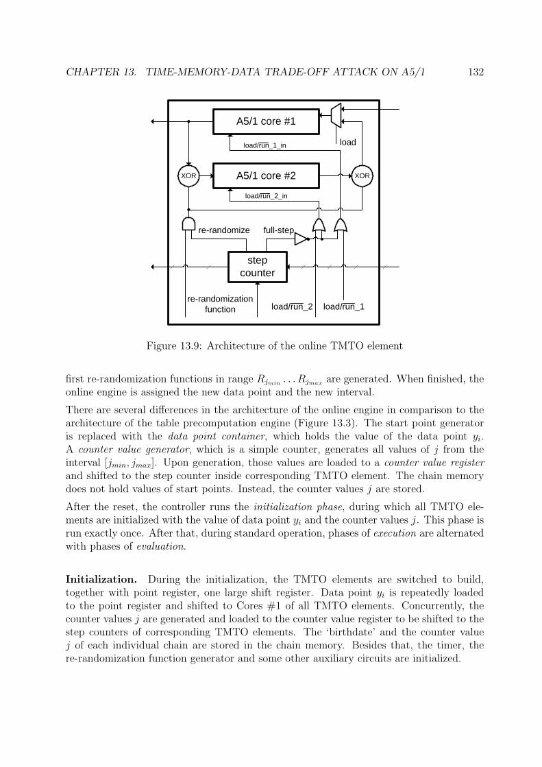
CHAPTER 13. TIME-MEMORY-DATA TRADE-OFF ATTACK ON A5/1 132
XOR
A5/1 core #1
A5/1 core #2 XOR
load
load/run_2_in
load/run_1_in
step counter
re-randomize
re-randomizationfunction
full-step
load/run_2 load/run_1
Figure 13.9: Architecture of the online TMTO element
first re-randomization functions in range Rjmin. . . Rjmax are generated. When finished, the
online engine is assigned the new data point and the new interval.
There are several differences in the architecture of the online engine in comparison to thearchitecture of the table precomputation engine (Figure 13.3). The start point generatoris replaced with the data point container, which holds the value of the data point yi.A counter value generator, which is a simple counter, generates all values of j from theinterval [jmin, jmax]. Upon generation, those values are loaded to a counter value registerand shifted to the step counter inside corresponding TMTO element. The chain memorydoes not hold values of start points. Instead, the counter values j are stored.
After the reset, the controller runs the initialization phase, during which all TMTO ele-ments are initialized with the value of data point yi and the counter values j. This phase isrun exactly once. After that, during standard operation, phases of execution are alternatedwith phases of evaluation.
Initialization. During the initialization, the TMTO elements are switched to build,together with point register, one large shift register. Data point yi is repeatedly loadedto the point register and shifted to Cores #1 of all TMTO elements. Concurrently, thecounter values j are generated and loaded to the counter value register to be shifted to thestep counters of corresponding TMTO elements. The ‘birthdate’ and the counter valuej of each individual chain are stored in the chain memory. Besides that, the timer, there-randomization function generator and some other auxiliary circuits are initialized.

CHAPTER 13. TIME-MEMORY-DATA TRADE-OFF ATTACK ON A5/1 133
XOR
A5/1 core #1
A5/1 core #2 XOR
load
load/run_2_in
load/run_1_in
TMTO element
TMTO element
TMTO element
point register
data point container
CONTROLLER
re-randomization function
generator
chain memory(counter value,
birthdate)
FIFO
DPchecker
timer
CO
NT
RO
L &
EV
ALU
AT
ION
EX
EC
UT
ION
step counter
re-randomize
re-randomizationfunction
full-step
load/run_2 load/run_1
counter value generator
counter value register
Figure 13.10: Architecture of an A5/1 online engine

CHAPTER 13. TIME-MEMORY-DATA TRADE-OFF ATTACK ON A5/1 134
Execution. Execution itself is performed in TMTO elements. One phase of executionlasts exactly one rainbow sequence. The function has been already described in Subsec-tion 13.4.1.
Evaluation. When the rainbow sequence is finished, all TMTO elements are againswitched into one large shift register and the results are shifted-out. The results are on-the-fly checked for the DP-property, and the length of each chain is calculated as a differencebetween a ‘current date’ (which is the current value of the timer) and the ‘birthdate’ of thecorresponding chain, which is stored in the chain memory. For each chain, one of followingthree cases may appear:
1. If the result satisfies the DP-property (it is the end point) and if the length l ofthe chain does not exceed the maximum length of chain, l ≤ tmax, then the chaininformation (end point, length, counter value) is stored into FIFO — the value of theend point is acquired from the point register and the counter value is acquired fromthe chain memory.
Concurrently, the end point, held in the point register, is replaced with the data pointyi, and a new counter value is generated and loaded to the counter value register. Atthe same moment both the new counter value and the ‘birthdate’ are stored in thechain memory.
Information stored in FIFO is later read out by the host computer and stored on thedisk.
2. If the chain becomes too large, l > tmax, then the chain is discarded and the genera-tion of a new chain is initiated in the same TMTO element — the procedure is thesame as above, but the chain information is not stored in FIFO.
3. In all other cases (i.e. the end point has not been achieved and the chain is not toolong yet) the result is simply shifted back to the TMTO element to continue withthe next rainbow sequence.
During the phase of evaluation we also initialize the re-randomization function generatorto generate the same rainbow sequence in the next phase of execution.
Unlike the precomputation phase, the loss of any chain information would be harmfulin the online phase. Therefore, if the FIFO becomes full, then the phase of evaluation isinterrupted until some space in FIFO is released. The data transfered to the host computerare again encoded with the Hamming code, however, in this case we use it as a SEC-DEDcode.

CHAPTER 13. TIME-MEMORY-DATA TRADE-OFF ATTACK ON A5/1 135
13.4.3 Implementation Results
In comparison to the precomputation TMTO element, the online TMTO element occupieslarger area , as it is extended by the step counter. Therefore, we were able to place only160 online TMTO elements on one FPGA. For a higher complexity of the design, the max-imum achievable frequency was only 80 MHz. If the number of online TMTO elementswas decreased to just 120 of them, the maximum achievable frequency was increased to120 MHz, since synthesis and implementation tools were able to better utilize some opti-mization techniques (register replication, better routing etc.). We have selected the secondimplementation, as it has 12.5% higher performance than the first one.
Let’s summarize: the A5/1 online engine can run at a maximum frequency of 120 MHz.Computing the step-function fi takes 64 clock cycles. One FPGA contains 120 TMTOelements, the whole COPACOBANA contains 120 FPGAs. Therefore, the whole COPA-COBANA can perform
120× 120× 120 · 106
64≈ 234.65
step-functions per second in the online phase. Values of online time T for different sets ofparameters are summarized in Table 13.1.
13.5 Fast Search at Disk-Stored TMTO Tables
Distinguished points calculated by COPACOBANA in the online phase are looked-up inthe TMDTO table. If the table is stored on the disk, then simple binary search methodcannot be used, as it needs several tens of hours.
Example 13.3. For example, upon selecting parameters presented in the third rowof Table 13.1, we generate the TMDTO table containing information on m = 238.52
chains. Binary search needs 39 table accesses to accomplish one look-up in sucha table. Since the disk access lasts about 8 ms on average, we would need up to220× 39× 8 ms ≈ 327156 s ≈ 91 hours to look-up 220 entries calculated in the onlinephase.
This approach takes even longer time than simple reading of the whole table. Asthe table occupies M = 4.85 TB and the disk data rate is stated to be fB = 100 MB/s,the whole table may be read (and data checked for the presence of any calculatedresult) in just 4850000 MB
100 MB/s = 48500 s ≈ 13.5 hours.
To improve look-ups, we use a method discussed in [Bal08]. The TMDTO table is dividedinto “sectors” of equal length. The values of the end points (keys) at the sector bordersare stored in a separate table, as shown in Figure 13.11. The length of the sector is chosen

CHAPTER 13. TIME-MEMORY-DATA TRADE-OFF ATTACK ON A5/1 136
TMDTO table divided into sectors
Border points stored in a separate table
sect
or
Figure 13.11: The TMDTO table is divided into sectors. Border points are stored in aseparate table.
to be as small as possible; it is limited only by maximum possible number of sectors, asthe table containing border points must fit into RAM installed in the computer.
Before starting search of entries calculated by COPACOBANA, the table containing borderpoints is loaded from the disk to RAM. For each entry, we first run the binary search inthe RAM table to find in which sector the entry is potentially found. Then the wholesector is loaded from the disk into RAM and the search is finalized. Since the sector isrelatively small, loading the whole sector takes shorter time than one disk access. Binarysearch performed in RAM is also very fast. Therefore, time for one table look-up is almostequal to one disk access.
To further accelerate search, we sort entries calculated by COPACOBANA prior to theirsearch in TMDTO table. This improvement reduces an average disk seek time, since thedisk heads are moved only in one direction and for shorter distances. Concretely, wemeasured an average access time to be about 12 ms when the entries were unsorted. Thistime was reduced to about 4 ms after sorting the entries.
Example 13.4. Let’s assume that we have a computer equipped with 16 GB of RAM.Such memory may hold at least 231 end points. Then the TMDTO table presented inthe third row of Table 13.1 may be divided into the same number of sectors, each being2.425 kB long. Searching all 220 entries then lasts about 220 × 4 ms ≈ 4194 s ≈ 1.2hour.

CHAPTER 13. TIME-MEMORY-DATA TRADE-OFF ATTACK ON A5/1 137
To further reduce the search time, the TMDTO table may be divided among N disks toperform the search in parallel. For example, if N = 10, then for above Example 13.4 thesearch time is reduced to about 7 minutes.
Nevertheless, we think that this Section will be soon outdated. Growing capacities anddramatically dropping prices of Flash memories inevitably lead to a replacement of the diskswith this kind of storage elements. For example, 1 GB of Flash memory can be currently(January 2009) purchased for less than 2 e. Therefore, the Flash memory of a total capacity4.85 TB (the third row of Table 13.1) may be currently purchased for less than 10,000 e,which is feasible not only for government agencies, but also for many other institutions andprivate persons. The same capacity at the disks may be currently purchased for less than500 e. In contrast to the disks, the Flash memories provide significantly faster randomaccess, which allows efficient implementation of the binary search. On the other hand,they suffer from frequent rewriting its content, which is not, however, our case.
13.6 Summary and Final Remarks
In this Chapter we presented a time-memory-data trade-off attack on A5/1 cipher. Theattack accepts known keystream, revealing, with a certain probability, the internal stateproducing such a keystream. The attack is supported by a low-cost special-purpose hard-ware device COPACOBANA in both the precomputation and online phases. Upon theanalysis described in Chapter 12, we have selected the thin-rainbow method to be used forour attack.
When designing the precomputation engine we employed the features of the underlyingFPGA architecture to gain maximum performance of the engine. The architecture ap-proach that we used might be reused when designing similar engines for cryptanalysis ofstream ciphers. COPACOBANA is able to perform 236 step functions per second in a pre-computation phase — each one of 120 FPGAs performs about 229 step functions per second.To compare, a current PC is able to perform just 222 step-function per second [BBK06].When assuming purchase price of COPACOBANA to be 10,000 e, and the purchase priceof a current PC to be 200 e, we obtain about 330 times better cost-performance ratio infavor of COPACOBANA. We get even better comparison when assuming variable costsrepresented mainly by energy consumption. For example, if we assume that fully equippedCOPACOBANA consumes less than 600 W of power, and the PC consumes about 150 Wof power, than we get about 4,000 times better consumption-performance ratio in favor ofCOPACOBANA.
Besides a careful design of the precomputation engine, we also designed the online engine.COPACOBANA is able to perform 234.65 step-functions per second in the online phase.We also brought solutions for the problems of an efficient sort of large disk-stored tables,as well as fast look-ups in such large tables.
We have selected a set of parameters providing a reasonable precomputation time and

CHAPTER 13. TIME-MEMORY-DATA TRADE-OFF ATTACK ON A5/1 138
a reasonable size of the tables, as well as a relatively small number of table accesses.For our selection of parameters, we obtain a precomputation time of 95.4 days and thememory capacity of 4.85 TB. As this is a probabilistic attack, success rate, as well asonline complexity and the number of table accesses depend on the number of data samplesavailable. If the number of data points available is D = 64, then the success rate isPtotal = 63%, COPACOBANA calculates all results in 27.6 seconds, and the results arethen looked-up in 10 disks in less than 7 minutes. If the number of data points increasesto D = 204, then the success rate is Ptotal = 96%, however, also the time for calculationsin COPACOBANA increases to 88 seconds and the time for table look-ups in 10 disksincreases to about 22.3 minutes.
Due to a reduced communication bandwidth caused by technical problems with the inter-face, we decided to use another set of parameters for our initial implementation. We haverun a series of measurements for data sets of different sizes. The measurements confirmthat, as predicted, the average chain length l′avg decreases after the rejection of (shorter)chains with duplicate end points. This decrease is stronger with a larger set of chains.We also measured how the number of (chains with) unique end points m depends on thenumber of generated chains m′. As has been shown, theoretical results were too optimistic.In reality the chain merges are more frequent, which is mainly caused by non-injective be-havior of A5/1 cipher. We have identified one source of merges — by careful generation ofstart points, this source can be eliminated.
We have run several functional tests of the online phase to verify correctness of the imple-mentation. To evaluate the statistical behavior of the attack — mainly the success ratio —extensive tests of the online phase are necessary. We expect these tests to be significantlytime consuming. For example, for the above assumed parameters we calculated the timenecessary for table look-ups to be about 22.3 minutes. Therefore, running table look-upsfor 1000 instances of this attack is expected to last about 15.5 days.
Similarly to the attack presented in Chapter 11 this attack recovers the internal statewhich generated some of given 64-bit data points (keystream samples). In comparison tothe attack presented in Chapter 11, this recovery is done significantly faster (in a matter ofseconds or minutes), on the other hand, there is certain probability that no internal stateis revealed. Moreover, successful recovery of one internal state does not ensure successfulattack, since, as shown, multiple distinct internal states may generate identical keystream.
To break GSM communication, the cipher needs to be tracked back from recovered state(s)to evaluate the internal state in which the cipher appeared just after loading the sessionkey K. Backtracking of A5/1 cipher is discussed in Chapter 14.

Chapter 14
Backtracking A5/1
Internal state recovery is sufficient for breaking many stream ciphers [BS00]. The ciphercan be then run forward from the revealed internal state (xr), decrypting the remainder ofthe ciphertext. Since the GSM communication is divided into 114 bits long frames, onlythe recovery of a single internal state is not sufficient — we would be able to decrypt theremainder of one frame, while other frames would remain encrypted.
To break the whole phone call we have to find either the session key K or some internalstate which is common for all frames. Such an internal state is the state just after loadingthe session key, xk. In this Chapter we discuss how the recovered internal state xr can beused for derivation of the state xk.
In the following text the symbol xn denotes the internal state, i.e. the contents of all threeregisters R1, R2 and R3. The symbol xn+` then denotes the internal state obtained fromxn by running the A5/1 cipher for ` clock cycles.
14.1 Detailed View on Algorithm of A5/1
Let’s recapitulate the algorithm of A5/1 cipher. The sequence of internal states is depictedin Figure 14.1.
At the beginning of each frame, the contents of all three LFSRs R1, R2 and R3 is cleared.Then, the 64 bit session key K is loaded to the registers R1, R2 and R3; the i-th bit ofthe key K is XORed with LSBs of all 3 registers in the i-th clock cycle. Let xk be theinternal state after loading the key K. Since the session key K is common for all frames ofthe same phone call, also the internal state xk is common for all frames of the same phonecall. Therefore, with the knowledge of xk, the phone call can be decrypted.
The initialization phase continues with loading the initialization vector IV . Again, 22 bitsof IV are successively added modulo 2 to LSBs of all 3 registers. Let xi be the internalstate after loading IV . Since the initialization vector IV is derived from the publicly known
139

CHAPTER 14. BACKTRACKING A5/1 140
0K−−−−−−−−→
64 clock cyclesxk
IV−−−−−−−−→22 clock cycles
xiwarm−up−−−−−−−−−→
100 clock cyclesxw −−−−−−−→
1 clock cyclexe
Figure 14.1: Sequence of internal states in A5/1
frame number FN , it is possible to derive xk, whenever xi is known — to obtain xk fromthe known xi, we need to clock registers R1, R2 and R3 backwards and to subtract bits ofIV in a reverse order.
The initialization phase is followed by the warm-up phase, which lasts 100 clock cycles.During this phase the registers are irregularly clocked and the output is discarded. Letxw = xi+100 be the internal state after the warm-up phase.
In the executional phase, the registers are also clocked irregularly. In each clock cycle, theregisters are clocked first and then the keystream bit is generated. Let xe = xw+1 = xi+101
be the internal state producing the first bit of the keystream, which is also the internal stateassociated with the first 64-bit keystream sample y0 by the function g in Equation 12.37.
The cipher produces two 114 bits long keystreams used to encrypt uplink frame and todecrypt downlink frame. In the following we assume that the first of two keystreams isknown. From 114 bits long keystream, we can derive 51 keystream samples y0 . . . y50, eachbeing 64 bits long, as shown in Figure 12.3. These samples were produced from the internalstates xe . . . xe+50. Our methods, described in Chapters 11 and 13, focus on finding xe+`for a given y`, 0 ≤ ` ≤ 50. When the state xe+` = xi+101+` is found, we have to derivecorresponding xk or, equivalently, xi. Upon recovering xk the GSM communication can bedecrypted.
14.2 Previous Work
The method described in [Gen08] derives xi from xe, however it is extendable for any xe+`.From the internal state xe Gendrullis calculates all 101 predecessor states for each registerR1, R2 and R3. By combining all predecessor states he produces all 1013 ≈ 220 candidatesfor the state xi. From each xi candidate, the cipher is clocked for 101 clock cycles andthe internal state obtained is compared with xe. If the match is obtained, then the validcandidate for xi has been found.
The algorithm finds 95% of xi candidates in ≈ 220 steps. To find all candidates, thealgorithm has to perform 1013 × 101 ≈ 227 steps.
In this chapter we describe the method with a maximum measured complexity of ≈ 213
steps for xe and ≈ 214 steps for xe+50. The method is based on the work of Golic [Gol97].

CHAPTER 14. BACKTRACKING A5/1 141
14.3 Proposed Method
The idea of the algorithm described here consists in clocking the cipher from the state xe+`backwards to the state xi. Each internal state has up to 4 potential predecessors, therefore,when backtracking the cipher we may search a tree having up to 4101+` leaves. However,this may happen only when the internal state of the cipher consists of all ‘1’s or all ‘0’swhich is almost improbable and may be easily detected.
When searching all potential predecessors xn−1 of the internal state xn we have to inspectbits R1[9], R1[8], R2[11], R2[10], R3[11] and R3[10] of the state xn, since following 4combinations of these 6 bits could create a triple of the clocking bits of the state xn−1:
• {R1[9], R2[11], R3[11]} (all 3 registers were clocked in the state xn−1)
• {R1[9], R2[11], R3[10]} (R1 and R2 clocked, R3 stopped in the state xn−1)
• {R1[9], R2[10], R3[11]} (R1 and R3 clocked, R2 stopped in the state xn−1)
• {R1[8], R2[11], R3[11]} (R2 and R3 clocked, R1 stopped in the state xn−1)
Table 14.1 shows three examples of internal states and their potential predecessor states.Only bits R1[9], R1[8], R2[11], R2[10], R3[11] and R3[10] and their position in the poten-tial predecessor states are shown. As obvious, only some predecessor states are possible(denoted by O.K.), while the other ones are impossible to occur (denoted by n/a). Forexample, the state xn in Ex. 1 could not be reached from the state xn−1 by clocking regis-ters R2 and R3 only (Candidate No. 3) — if we clock registers R2 and R3 back from thestate xn, we obtain the state candidate xn−1 having all clocking bits being ‘0’. Applyingthe clocking rule, we have to clock all 3 registers now, therefore the successor of CandidateNo. 3 is different from xn.
As obvious from our examples in Table 14.1, some internal states have only few or even no(see Ex. 3) predecessor states. We can formulate the following set of rules:
• If R1[9] = R2[11] = R3[11], then the predecessor state xn−1 obtained from the statexn by clocking back the registers R1, R2 and R3 is valid
• If R1[9] = R2[11] 6= R3[10], then the predecessor state xn−1 obtained from the statexn by clocking back the registers R1 and R2 only is valid
• If R1[9] = R3[11] 6= R2[10], then the predecessor state xn−1 obtained from the statexn by clocking back the registers R1 and R3 only is valid
• If R2[11] = R3[11] 6= R1[8], then the predecessor state xn−1 obtained from the statexn by clocking back the registers R2 and R3 only is valid

CHAPTER 14. BACKTRACKING A5/1 142
Table 14.1: Three examples of the internal states and the candidates for their predecessors.Clocking bits are highlighted.
Example Example Example1 2 3
R1[9] R1[8] 0 0 0 0 0 0State xn R2[11] R2[10] 0 1 0 0 0 1
R3[11] R3[10] 0 1 1 1 1 0
Can
did
ates
for
stat
exn−
1
No. 1
clock R1+R2 O.K. O.K. n/aR1[8] R1[7] 0 0 0 0 0 0R2[10] R2[9] 0 1 0 0 0 1
R3[11] R3[10] 0 1 1 1 1 0
No. 2
clock R1+R3 O.K. n/a n/aR1[8] R1[7] 0 0 0 0 0 0
R2[11] R2[10] 0 1 0 0 0 1R3[10] R3[9] 0 1 1 1 1 0
No. 3
clock R2+R3 n/a n/a n/aR1[9] R1[8] 0 0 0 0 0 0
R2[10] R2[9] 0 1 0 0 0 1R3[10] R3[9] 0 1 1 1 1 0
No. 4
clock R1+R2+R3 O.K. n/a n/aR1[8] R1[7] 0 0 0 0 0 0R2[10] R2[9] 0 1 0 0 0 1R3[10] R3[9] 0 1 1 1 1 0
# Candidates 3 1 0

CHAPTER 14. BACKTRACKING A5/1 143
Algorithm 14.1 BACKWARD STEP(R1, R2, R3, DEPTH) — a recurrent procedure forA5/1 backtracking
Input: Internal state (registers R1, R2, R3); DEPTH (#steps until xi)Output: All candidates for the state xi
1: if DEPTH = 0 then2: return R1, R2, R33: else4: R1back ← CLOCK BACKWARDS(R1)5: R2back ← CLOCK BACKWARDS(R2)6: R3back ← CLOCK BACKWARDS(R3)7: if R1[9] = R2[11] = R3[11] then8: BACKWARD STEP (R1back, R2back, R3back, DEPTH − 1)9: end if
10: if R1[9] = R2[11] 6= R3[10] then11: BACKWARD STEP (R1back, R2back, R3, DEPTH − 1)12: end if13: if R1[9] = R3[11] 6= R2[10] then14: BACKWARD STEP (R1back, R2, R3back, DEPTH − 1)15: end if16: if R2[11] = R3[11] 6= R1[8] then17: BACKWARD STEP (R1, R2back, R3back, DEPTH − 1)18: end if19: end if
Tables 14.2 and 14.3 summarize all 64 combinations of bits R1[9], R1[8], R2[11], R2[10],R3[11] and R3[10] of the state xn. For each combination, all valid candidates for thepredecessor states are enumerated. As obvious, only for 2 combinations (all ‘0’s and all‘1’s), which represent only 3.125% of all cases, we obtain 4 valid predecessors. For 6combinations (9.375%), we get 3 predecessors, for another 6 combinations (9.375%), weget 2 predecessors, for 26 combinations (40.625%), we get only one predecessor, and 24combinations (37.5%) do not have any valid predecessor. All 64 combinations have in total64 predecessors, i.e. each internal state has one predecessor on average.
Based on these observations, we propose a recurrent procedure BACKWARD STEPdepicted in Algorithm 14.1. The procedure is invoked with the initial parametersR1, R2 and R3 representing the internal state xe+` = xi+101+`, and the parameterDEPTH = 101 + `. The procedure outputs all candidates for the state xi. The functionCLOCK BACKWARDS used in the procedure returns the value of the register clockedback by one clock cycle.

CHAPTER 14. BACKTRACKING A5/1 144
Table 14.2: Predecessors of the states — part 1
State xn Candidatesfor the state xn−1 # Cand.
(important bit values) (by clocking)R1[9] R1[8] R1 R1 R2
R2[11] R2[10] + + + allR3[11] R3[10] R2 R3 R3
0 0 0 0 0 0√
10 0 0 0 0 1
√ √2
0 0 0 0 1 0 00 0 0 0 1 1
√1
0 0 0 1 0 0√ √
20 0 0 1 0 1
√ √ √3
0 0 0 1 1 0 00 0 0 1 1 1
√1
0 0 1 0 0 0 00 0 1 0 0 1 00 0 1 0 1 0
√1
0 0 1 0 1 1√
10 0 1 1 0 0
√1
0 0 1 1 0 1√
10 0 1 1 1 0
√1
0 0 1 1 1 1√
10 1 0 0 0 0
√ √2
0 1 0 0 0 1√ √ √
30 1 0 0 1 0 00 1 0 0 1 1
√1
0 1 0 1 0 0√ √ √
30 1 0 1 0 1
√ √ √ √4
0 1 0 1 1 0 00 1 0 1 1 1
√1
0 1 1 0 0 0 00 1 1 0 0 1 00 1 1 0 1 0 00 1 1 0 1 1 00 1 1 1 0 0
√1
0 1 1 1 0 1√
10 1 1 1 1 0 00 1 1 1 1 1 0
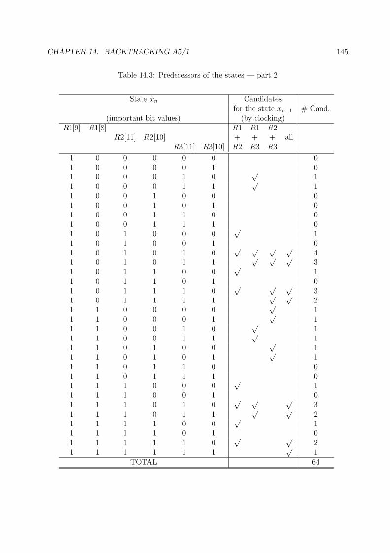
CHAPTER 14. BACKTRACKING A5/1 145
Table 14.3: Predecessors of the states — part 2
State xn Candidatesfor the state xn−1 # Cand.
(important bit values) (by clocking)R1[9] R1[8] R1 R1 R2
R2[11] R2[10] + + + allR3[11] R3[10] R2 R3 R3
1 0 0 0 0 0 01 0 0 0 0 1 01 0 0 0 1 0
√1
1 0 0 0 1 1√
11 0 0 1 0 0 01 0 0 1 0 1 01 0 0 1 1 0 01 0 0 1 1 1 01 0 1 0 0 0
√1
1 0 1 0 0 1 01 0 1 0 1 0
√ √ √ √4
1 0 1 0 1 1√ √ √
31 0 1 1 0 0
√1
1 0 1 1 0 1 01 0 1 1 1 0
√ √ √3
1 0 1 1 1 1√ √
21 1 0 0 0 0
√1
1 1 0 0 0 1√
11 1 0 0 1 0
√1
1 1 0 0 1 1√
11 1 0 1 0 0
√1
1 1 0 1 0 1√
11 1 0 1 1 0 01 1 0 1 1 1 01 1 1 0 0 0
√1
1 1 1 0 0 1 01 1 1 0 1 0
√ √ √3
1 1 1 0 1 1√ √
21 1 1 1 0 0
√1
1 1 1 1 0 1 01 1 1 1 1 0
√ √2
1 1 1 1 1 1√
1TOTAL 64

CHAPTER 14. BACKTRACKING A5/1 146
0%
1%
2%
3%
4%
5%
6%
0 5 10 15 20 25 30 35 40 45
>49
# candidates
0%
2%
4%
6%
8%
10%
12%
14%
0-99
100-
199
200-
299
300-
399
400-
499
500-
599
600-
699
700-
799
800-
899
900-
999
1000
-109
911
00-1
199
1200
-129
913
00-1
399
1400
-149
915
00-1
599
1600
-169
917
00-1
799
1800
-189
919
00-1
999
2000
-209
921
00-2
199
2200
-229
923
00-2
399
2400
-249
9>
2499
# steps
Figure 14.2: Test 1: a) Histogram of the candidates for the state xi, b) Histogram of thenumber of steps to seek the whole search tree
14.4 Testing the Method for A5/1 Backtracking
To observe the statistical behavior of the method we have run the set of following tests.
14.4.1 Test 1: Clocking A5/1 Forward and Backward for 101Clock Cycles
From randomly generated state xi, we derived the state xe by (forward) clocking the cipherfor 101 clock cycles. Then, using the procedure BACKWARD STEP, we clocked the cipherback to the depth of 101 clock cycles. For each individual case, we observed the numberof candidates for the state xi (one of them was the original xi), and the number of stepsto seek through the whole search tree.
The test was run for 108 (pseudo)random cases. An average and a maximum number ofcandidates for the state xi was 13.13 and 170, respectively. A histogram of the candidatesfor the internal state xi is depicted in Figure 14.2a. An average and a maximum numberof steps to seek the whole search tree was 717.24 and 8019, respectively. A histogram ofthe number of steps is depicted in Figure 14.2b.
14.4.2 Test 2: Clocking A5/1 Forward and Backward for 151Clock Cycles
From randomly generated state xi, we derived the state xe+50 by clocking the cipher (for-ward) for 151 clock cycles. Then, using the procedure BACKWARD STEP, we clockedthe cipher back to the depth of 151 clock cycles. For each individual case, we observed thenumber of candidates for the state xi (one of them was the original xi), and the numberof steps to seek through the whole search tree.

CHAPTER 14. BACKTRACKING A5/1 147
0%
1%
2%
3%
4%
5%
6%
0 5 10 15 20 25 30 35 40 45
>49
# candidates
0%
2%
4%
6%
8%
10%
12%
14%
0-99
100-
199
200-
299
300-
399
400-
499
500-
599
600-
699
700-
799
800-
899
900-
999
1000
-109
911
00-1
199
1200
-129
913
00-1
399
1400
-149
915
00-1
599
1600
-169
917
00-1
799
1800
-189
919
00-1
999
2000
-209
921
00-2
199
2200
-229
923
00-2
399
2400
-249
9>
2499
# steps
Figure 14.3: Test 2: a) Histogram of the candidates for the state xi, b) Histogram of thenumber of steps to seek the whole search tree
The test was run for 108 (pseudo)random cases. An average and a maximum number ofcandidates for the state xi was 18.04 and 207, respectively. A histogram of the candidatesfor the internal state xi is depicted in Figure 14.3a. An average and a maximum numberof steps to seek the whole search tree was 1448.71 and 14885, respectively. A histogram ofthe number of steps is depicted in Figure 14.3b.
14.4.3 Test 3: Clocking A5/1 Backward Only for 101 Clock Cy-cles
From randomly generated state xe, we clocked the cipher back to the depth of (up to) 101clock cycles. For each individual case, we observed the number of candidates for the statexi, the number of steps to seek through the whole search tree and the maximum depthreached in the search tree.
The test was run for 108 (pseudo)random cases. As obvious from Figure 14.4, only in 15%of cases the search reached the depth of 101 clock cycles and a candidate for the state xihas been found, while other 85% cases led to no candidate (see also Figure 14.5a). It isalso obvious from Figure 14.4 that in 37.5% cases the depth of the search tree was 0, whichcorresponds to our observations presented in Tables 14.2 and 14.3.
If at least one candidate for the state xi has been found, then the average number ofcandidates was 6.65. The maximum number of candidates was 128. The average depth ofthe search tree was 28.45 steps.
An average number of steps to seek the whole search tree was 101.00, which conforms toobservation that each internal state has one predecessor on average (see Section 14.3). Themaximum number of steps to seek the whole search tree was 6518. A histogram of thenumber of steps is depicted in Figure 14.5b.

CHAPTER 14. BACKTRACKING A5/1 148
0%
5%
10%
15%
20%
25%
30%
35%
40%0 5 10 15 20 25 30 35 40 45 50 55 60 65 70 75 80 85 90 95 100
# depth
Figure 14.4: Test 3: Histogram of the maximum depth reached in the search tree
0%
10%
20%
30%
40%
50%
60%
70%
80%
90%
0 1 2 3 4 5 6 7 8 9 10 11 12 13 14 15 16 17 18 19
>19
# candidates
0%
10%
20%
30%
40%
50%
60%
70%
80%
0-99
100-
199
200-
299
300-
399
400-
499
500-
599
600-
699
700-
799
800-
899
900-
999
>99
9
# steps
Figure 14.5: Test 3: a) Histogram of the candidates for the state xi, b) Histogram of thenumber of steps to seek the whole search tree

CHAPTER 14. BACKTRACKING A5/1 149
0%
5%
10%
15%
20%
25%
30%
35%
40%
0 7 14 21 28 35 42 49 56 63 70 77 84 91 98 105
112
119
126
133
140
147
# depth
Figure 14.6: Test 4: Histogram of the maximum depth reached in the search tree
14.4.4 Test 4: Clocking A5/1 Backward Only for 151 Clock Cy-cles
From randomly generated state xe+50, we clocked the cipher back to the depth of (up to)151 clock cycles. For each individual case, we observed the number of candidates for thestate xi, the number of steps to seek through the whole search tree and the maximumdepth reached in the search tree.
The test was run for 108 (pseudo)random cases. As obvious from Figure 14.6, only in 10.9%of cases the search reached the depth of 151 clock cycles and a candidate for the state xihas been found, while other 89.1% cases led to no candidate (see also Figure 14.7a). It isalso obvious from Figure 14.6 that in 37.5% cases the depth of the search tree was 0, whichcorresponds to our observations presented in Tables 14.2 and 14.3.
If at least one candidate for the state xi has been found, then the average number ofcandidates was 9.19. The maximum number of candidates was 151. The average depth ofthe search tree was 34.80 steps. An average and a maximum number of steps to seek thewhole search tree was 151.05 and 11272, respectively. A histogram of the number of stepsis depicted in Figure 14.7b.

CHAPTER 14. BACKTRACKING A5/1 150
0%
10%
20%
30%
40%
50%
60%
70%
80%
90%
100%
0 1 2 3 4 5 6 7 8 9 10 11 12 13 14 15 16 17 18 19
>19
# candidates
0%
10%
20%
30%
40%
50%
60%
70%
80%
0-99
100-
199
200-
299
300-
399
400-
499
500-
599
600-
699
700-
799
800-
899
900-
999
>99
9
# steps
Figure 14.7: Test 4: a) Histogram of the candidates for the state xi, b) Histogram of thenumber of steps to seek the whole search tree
14.5 Summary and Final Remarks
The method described here has an average complexity of ≈ 210 steps and a maximummeasured complexity of ≈ 213 steps when backtracking the state xi from the state xe (Test1 and Test 3), which represents a very small stretch of time. Running 108 instances ofTest 1 and Test 2 took 15 hours and 30 hours, respectively, on an Intel Pentium Dual CPUT2390 1.86 GHz. One instance took 0.54 ms and 1.08 ms, respectively, on average.
The tests reveal one potential problem in cryptanalysis of A5/1. Due to non-injectivityof the cipher the number of candidates for the state xi is relatively high. The number ofcandidates for xi is about 10 on average, reaching about 200 in the worst case. From eachcandidate for xi the candidate for xk is derived by clocking the registers R1, R2 and R3back and subtracting the bits of initialization vector in reverse order. Then, each candidatefor xk must be tested by trial decryption of other frames.
There is an alternative way for identification of the valid xk. If we were able to recoverinternal states in two distinct frame keystreams of the same phone call, then we wouldderive two sets of candidates for xk. Since all frames of the same phone call share the samestate xk, then the valid xk would lie in an intersection of both sets.

Chapter 15
Conclusions of Part II
In this part we focused on cryptanalysis of GSM communication. The data transfersbetween the base transceiver station and the mobile phone are divided into 114 bit frames,encrypted with the stream cipher A5/1. Each frame is encrypted by its own keystream,generated with the usage of a common session key K and unique initialization vector IV .
We have presented two attacks and their implementation for the low-cost FPGA-basedsuper-computing cluster COPACOBANA. Like many other attacks on stream ciphers, alsoour two attacks reveal the internal state that generated a given known keystream. Sincethe GSM communication is divided into frames, the recovered internal state is then usedto derive the internal state xk common for all frames. The state xk represents the contentof internal registers after their reset and loading the session key K. In most cases thereare multiple candidates for the state xk (about 10 on average and about 200 at maximum),which can slightly complicate the attack.
The first of our two attacks belongs to the family of guess-and-determine attacks. Itreveals the internal state of the cipher in less than 6 hours on average demanding only64 bits of known keystream. The attack is based on the proposal made by Keller andSeitz, however, we made several modifications and improvements of the attack. While theattack of Keller and Seitz has only 18% success ratio, our attack recovers the internal statein 100% of cases. We also corrected some estimations made by Keller and Seitz. Ourattack is also very attractive with regard to financial costs which is a significant factorfor the practicability of an attack: The acquisition costs for COPACOBANA are about10,000 e. Since COPACOBANA has a maximum power consumption of only 600 W, theattack also features very low operational costs. For instance, assuming 10 cent per kWhthe operational costs of an attack are only 36 cents.
The second of our two attacks belongs to the family of time-memory-data tradeoff attacks.We have chosen the thin-rainbow method for the implementation. COPACOBANA is usedin both the precomputation phase and the online phase of the attack. When designing theprecomputation engine, we have utilized the features of underlying FPGA architectureto gain the maximum performance. The proposed design approach can be reused when
151

CHAPTER 15. CONCLUSIONS OF PART II 152
designing similar attacks on other stream ciphers. Besides designing the hardware architec-tures for the precomputation and online phases, we also discussed solutions for relativelyfast sort of a huge amount of acquired data and for relatively fast search in large table.The precomputation phase takes several month with one COPACOBANA; the TMDTOtable occupies several terabytes of memory. The online phase is then finished in a fractionof time — COPACOBANA executes all calculations in a matter of (tens of) seconds andsubsequent search of results in the TMDTO table is finished in a matter of minutes. Sincethis is a probabilistic attack, both the success ratio and the online complexity increasewith the amount of known keystream data.
Both attacks complement each other perfectly. Upon eavesdropping the GSM communica-tion and extraction of the keystream, we run fast TMDTO attack first. If the valid internalstate xk is not found (it is a probabilistic attack), then the (slower, but 100% successful)guess-and-determine attack is executed.
In our work we have not focused on eavesdropping GSM calls. Also the problem of obtaininga known plaintext is still under discussion in pertinent news groups and does not seem tobe fully solved. However, these are just some technical difficulties that certainly cannot beconsidered serious barriers for breaking GSM.

Acronyms and Symbols
All acronyms are defined when first used in the text, with the exception of frequently usedones.
A5/1 stream cipher used in GSM communicationASIC Application-Specific Integrated CircuitBTS Base Transceiver StationCB Clocking BitCLB Configurable Logic BlockCOPACOBANA Cost-Optimized Parallel Code BreakerCPU Central Processing UnitDCM Digital Clock ManagerDP Distinguished PointEC Elliptic CurveECC Elliptic Curve CryptographyDLP Discrete Logarithm ProblemECDLP Elliptic Curve Discrete Logarithm ProblemFIFO First-in First-out; queueFF Flip-FlopFPGA Field Programmable Gate ArrayFSM Finite State MachineGF (q) Finite Field (Galois Field)GSM Global System for Mobile communicationITT inversion algorithm invented by Itoh, Teechai and TsujiIV Initialization VectorLSB Least Significant BitLUT Look-Up TableLFSR Linear Feedback Shift RegisterMSB Most Significant BitMUX MultiplexerNB Normal Basis
153

CHAPTER 15. CONCLUSIONS OF PART II 154
NIST National Institute of Standards and TechnologyONB Optimal Normal BasisRAM Random Access MemoryRFID Radio-Frequency IDentificationRSA asymmetric cipher invented by Rivest, Shamir and AdlemanTMDTO Time-Memory-Data Trade-OffTMTO Time-Memory Trade-OffVHDL VHSIC Hardware Description LanguageVHSIC Very High Speed Integrated CircuitsVLSI Very Large Scale IntegrationXOR eXclusive OR (reduction modulo 2)

Bibliography
[AMOV91] G. B. Agnew, R. C. Mullin, I. M. Onyszchuk, and S. A. Vanstone. An imple-mentation for a fast public-key cryptosystem. Journal of Cryptology, pages63–79, 1991.
[And94] R. Anderson. A5 (was: Hacking digital phones). sci.crypt, 17 June 1994.
[ANR99] G. C. Ahlquist, B. Nelson, and M. Rice. Optimal Finite Field Multipliersfor FPGAs. In FPL 1999: Proceedings of the 9th International Workshopon Field Programmable Logic and Applications, pages 51–60, New York, NY,USA, 1999. Springer-Verlag New York, Inc.
[ANS97] ANSI. ANSI X9.30:1-1997, Public Key Cryptography for the Financial Ser-vices Industry: Part 1: The Digital Signature Algorithm (DSA) (revision ofX9.30:1-1995), 1997.
[ANS98a] ANSI. ANSI X9.31-1998, Digital Signatures Using Reversible Public KeyCryptography for the Financial Services Industry (rDSA), 1998.
[ANS98b] ANSI. ANSI X9.62-1998, Public Key Cryptography for the Financial ServicesIndustry: The Elliptic Curve Digital Signature Algorithm (ECDSA), 1998.
[Bab95] S. Babbage. A Space/Time Tradeoff in Exhaustive Search Attacks on StreamCiphers. In European Convention on Security and Detection, May 1995.
[Bal08] M. Balık. Methods of Fast Search in Disk Stored Tables. Private communi-cation via email, February 2008.
[BBK03] E. Barkan, E. Biham, and N. Keller. Instant Ciphertext-Only Cryptanalysisof GSM Encrypted Communications. In Proc. of Crypto’03, volume 2729 ofLNCS. Springer-Verlag, 2003.
[BBK06] E. Barkan, E. Biham, and N. Keller. Instant Ciphertext-only Cryptanalysis ofGSM Encrypted Communication (full-version). Technical Report CS-2006-07,Technion, 2006.
155

BIBLIOGRAPHY 156
[BBS06] E. Barkan, E. Biham, and A. Shamir. Rigorous Bounds on CryptanalyticTime/Memory Tradeoffs. In Proc. of CRYPTO’06, volume 4117 of LNCS,pages 1–21. Springer, 2006.
[BGW99] M. Briceno, I. Goldberg, and D. Wagner. A Pedagogical Implementation ofthe GSM A5/1 and A5/2 “voice privacy” Encryption Algorithms, 1999.
[BS00] A. Biryukov and A. Shamir. Cryptanalytic time/memory/data tradeoffs forstream ciphers. In Proc. of Asiacrypt’00, volume 1976 of LNCS, pages 1–13.Springer, 2000.
[BSGEG04] S. Bajracharya, C. Shu, K. Gaj, and T. El-Ghazawi. Implementation of Ellip-tic Curve Cryptosystems over GF (2n) in Optimal Normal Basis on a Recon-figurable Computer. In FPL2004: Proceeding of Field Programmable Logicand Applications, pages 1001–1005. Springer, 2004.
[BSW01] A. Biryukov, A. Shamir, and D. Wagner. Real Time Cryptanalysis of A5/1 ona PC. In Proc. of FSE’00, volume 1978 of LNCS, pages 1–18. Springer-Verlag,2001.
[Cer97] Certicom. The Elliptic Curve Cryptosystem. A Certicom Whitepaper, 1997.
[D. 82] D. E. R. Denning. Cryptography and Data Security. Addison-Wesley, 1982.
[DH76] W. Diffie and M. Hellman. New Directions in Cryptography. IEEE Transac-tions on Information Theory, 22:644–654, 1976.
[Ele98] Electronic Frontier Foundation. Cracking DES: Secrets of Encryption Re-search, Wiretap Politics & Chip Design. O’Reilly & Associates Inc., July1998.
[FIP00] FIPS. FIPS PUB 186-2, Digital Signature Standard, February 2000.
[Gao93] S. Gao. Normal Bases over Finite Fields. PhD thesis, University of Waterloo,Ontario, 1993.
[Gen08] Timo Gendrulis. Hardware-based cryptanalysis of the gsm a5/1 encryptionalgorithm. Master’s thesis, Ruhr University Bochum, 2008.
[Gol97] J. Golic. Cryptanalysis of Alleged A5 Stream Cipher. In Proc. of Eurocrypt’97,volume 1233 of LNCS, pages 239–255. Springer-Verlag, 1997.
[Gol00] J. Golic. Cryptanalysis of three mutually clock-controlled stop/go shift regis-ters. IEEE Transactions on Information Theory, 46:1081–1090, May 2000.
[GPP07] T. Gueneysu, C. Paar, and J. Pelzl. Attacking Elliptic Curve Cryptosystemswith Special-Purpose Hardware. In Proc. of FPGA’07, pages 207–215. ACMPress, 2007.

BIBLIOGRAPHY 157
[GS00] L. Gao and G.E. Sobelman. Improved VLSI designs for multiplication andinversion in GF (2M) over normal bases. In Proceedings of 13th Annual IEEEInternational ASIC/SOC Conference, pages 97–101, 2000.
[GWG99] I. Goldberg, D. Wagner, and L. Green. The Real-Time Cryptanalysis of A5/2.Presented at the Rump Session of Crypto’99, 1999.
[Hel80] M. E. Hellman. A Cryptanalytic Time-Memory Trade-off. IEEE Transactionson Information Theory, 26:401–406, 1980.
[Hsi70] M. Y. Hsiao. A Class of Optimal Minimum Odd-weight-column SEC-DEDCodes. IBM Journal of Research and Development, 14(4):395–401, 1970.
[IEE00] IEEE. IEEE 1363. Standard for Public-key Cryptography, 2000.
[ITT86] T. Itoh, O. Teechai, and S Tsujii. A Fast Algorithm for Computing Mul-tiplicative Inverses in GF (2t) using normal bases. J. Society for ElectronicCommunications (Japan), 44:31–36, 1986.
[KGKH04] S. Kwon, K. Gaj, C. H. Kim, and P. C. Hong. Efficient Linear Array for Mul-tiplication in GF (2m) Using a Normal Basis for Elliptic Curve Cryptography.In CHES 2004, volume LNCS 3156, pages 76–91. Springer-Verlag, 2004.
[Knu98] D. E. Knuth. The Art of Computer Programming, volume 3: Sorting andSearching. Addison-Wesley, 1998.
[Kob87] N. Koblitz. Elliptic curve cryptosystems. Mathematics of Computation,48:203–209, 1987.
[KPP+06] S. Kumar, C. Paar, J. Pelzl, G. Pfeiffer, and M. Schimmler. Breaking Cipherswith COPACOBANA - A Cost-Optimized Parallel Code Breaker. In Pro-ceedings of CHES’06, volume 4249 of LNCS, pages 101–118. Springer-Verlag,2006.
[KS98] C. Koc and B. Sunar. Low-Complexity Bit-Parallel Canonical and Normal Ba-sis Multipliers for a Class of Finite Fields. IEEE Transactions on Computers,47:353–356, 1998.
[KS01] J. Keller and B. Seitz. A Hardware-Based Attack on the A5/1 Stream Cipher,2001.
[Kwo03] S. Kwon. A low complexity and a low latency bit parallel systolic multi-plier over GF (2m) using an optimal normal basis of type II. In 16th IEEESymposium on Computer Arithmetic, pages 196–202, 2003.

BIBLIOGRAPHY 158
[LD99] J. Lopez and R. Dahab. Fast multiplication on elliptic curves over GF (2m)without precomputation. In Proceedings of the First International Workshopon Cryptographic Hardware and Embedded Systems (CHES), volume LNCS1717, pages 316–327. Springer-Verlag, 1999.
[LL02] P. H. W. Leong and I. K. H. Leung. A Microcoded Elliptic Curve ProcessorUsing FPGA Technology. IEEE Transactions on VLSI Systems, 10:550–559,2002.
[LL03] C. Lee and J. Lee. A Scalable Structure for a Multiplier and an Inversion Unitin GF (2m). ETRI Journal, 25:315–320, October 2003.
[LMWL00] K. H. Leung, K. W. Ma, W. K. Wong, and P. H. W. Leong. FPGA Imple-mentation of Microcoded Elliptic Curve Cryptographic Processor. In Pro-ceedings of the IEEE Symposium on Field-Programmable Custom ComputingMachines, pages 68–76, Napa Valley, California, USA, 2000.
[Mas97] MasterCard International, Inc. and Visa International Service Association.SET Secure Electronic Transaction Specification, May 31 1997.
[MBG+93] A. J. Menezes, I. F. Blake, XuHong Gao, R. C Mullin, S. A. Vanstone, andT. Yaghoobian. Applications of Finite Fields. Kluwer Academic Publishers,1993.
[Mil86] V. S. Miller. Use of elliptic curves in cryptography. In Advances in Cryptology- Crypto 85, volume LNCS 218, pages 417–426. Springer-Verlag, 1986.
[MO86] J. Massey and J. Omura. Computational Method and Apparatus for FiniteField Arithmetic. U.S. patent number 4,587,627, 1986.
[Mon87] P. Montgomery. Speeding the Pollard and elliptic curve methods of factoriza-tion. Mathematics of Computation, 48:243–264, 1987.
[MOVW89] R. Mullin, I. Onyszchuk, S. Vanstone, and R. Wilson. Optimal Normal Basesin GF (pn). Discrete Applied Mathematics, 22:149–161, 1989.
[Oec03] P. Oechslin. Making a Faster Cryptanalytic Time-Memory Trade-Off. In Proc.of CRYPTO’03, volume 2729 of LNCS, pages 617–630. Springer, 2003.
[Paa99] C. Paar. Implementation Options for Finite Field Arithmetic for EllipticCurve Cryptosystems. In ECC 1999, 1999.
[PS00] T. Pornin and J. Stern. Software-hardware Trade-offs: Application to A5/1Cryptanalysis. In Proc. of CHES’00, volume 1965 of LNCS, pages 318–327.Springer-Verlag, 2000.

BIBLIOGRAPHY 159
[RMH03] A. Reyhani-Masoleh and M. A. Hasan. Low Complexity Sequential NormalBasis Multipliers over GF (2m). In 16th IEEE Symposium on Computer Arith-metic (ARITH-16 ’03), pages 188–195, 2003.
[RSA78] R. L. Rivest, A. Shamir, and L. M. Adleman. A method for obtaining dig-ital signatures and public-key cryptosystems. Communications of the ACM,21:120–126, 1978.
[Rup08] Andy Rupp. Computational Aspects of Cryptography and Cryptanalysis. PhDthesis, Ruhr University Bochum, 2008.
[SK01] B. Sunar and C. K. Koc. An efficient optimal normal basis type II multiplier.IEEE Transactions on Computers, 50:83–88, 2001.
[SRQL02] F. Standaert, G. Rouvroy, J. Quisquater, and J. Legat. A Time-MemoryTradeoff using Distinguished Points: New Analysis & FPGA Results. InProc. of CHES’02, volume 2523 of LNCS, pages 596–611. Springer, 2002.
[SWPS08] J. Schrder, L. Wienbrandt, G. Pfeiffer, and M. Schimmler. Massively Paral-lelized DNA Motif Search on the Reconfigurable Hardware Platform COPA-COBANA. In Third IAPR International Conference on Pattern Recognitionin Bioinformatics (PRIB 2008), volume LNCS 5265, pages 436–447, 2008.
[Uni05] University of California, Berkeley. Seti@Home Website, 2005.
[Wal] M. Wall. M: GAlib: A C++ Library of Genetic Algorithm Components.[Online].
[Xil99] Xilinx. XC4000E and XC4000X Series Field Programmable Gate Arrays, May1999.
[Xil07] Xilinx. Spartan-3 FPGA Family: Complete Data Sheet, DS099, November2007.

Refereed Publications of the Author
[A.1] J. Schmidt, M. Novotny, M. Jager, M. Becvar, and M. Jachim. Exploration of DesignSpace in ECDSA. In Field-Programmable Logic and Applications 2002, LNCS 2438,pages 1072–1075. Springer Verlag, Montpellier 2002.
[A.2] J. Schmidt and M. Novotny. Normal Basis Multiplication and Inversion Unit forElliptic Curve Cryptography. In Proceedings of the 10th IEEE International Con-ference on Electronics, Circuits and Systems 2003, pages 82–85. IEEE, Piscataway2003.
[A.3] J. Schmidt and M. Novotny. Optimum Shifter Synthesis Using a Genetic Algorithm.In Recent Trends in Multimedia Information Processing, pages 146–149. Sdelovacıtechnika, Praha 2003.
[A.4] J. Schmidt and M. Novotny. Scalable Shifter Synthesis for a Finite Field ArithmeticUnit. In Proceedings of 7th IEEE Design and Diagnostics of Electronic Circuitsand Systems Workshop, pages 195–198. Institute of Informatics, Slovak Academy ofSciences, Bratislava, 2004.
[A.5] J. Schmidt and M. Novotny. Scalable Normal Basis Arithmetic Unit for EllipticCurve Cryptography. Acta Polytechnica, 45:55–60, 2005
[A.6] M. Novotny and J. Schmidt. General Digit-Serial Normal Basis Multiplier. In Pro-ceedings of 8th IEEE Design and Diagnostics of Electronic Circuits and SystemsWorkshop, pages 99–104. University of Western Hungary, Sopron, 2005.
[A.7] M. Novotny and J. Schmidt. Normal Basis Multipliers of General Digit Width Ap-plicable in ECC. In Proceedings of 9th IEEE Design and Diagnostics of ElectronicCircuits and Systems Workshop, pages 145–146. CTU Publishing House, Praha, 2006
[A.8] M. Novotny and J. Schmidt. General Digit Width Normal Basis Multipliers withCircular and Linear Structure. In Field-Programmable Logic and Applications -FPL2006, pages 873–876, Madrid 2006
[A.9] M. Novotny and J. Schmidt. Two Architectures of a General Digit-Serial NormalBasis Multiplier. In Proceedings of 9th Euromicro Conference on Digital SystemDesign, pages 550–553, IEEE Computer Society, Dubrovnik 2006
160

REFEREED PUBLICATIONS OF THE AUTHOR 161
[A.10] M. Novotny and J. Schmidt. General Digit-Serial Normal Basis Multiplier withDistributed Overlap. In Proceedings of 10th Euromicro Conference on Digital SystemDesign, pages 94–101, IEEE Computer Society, Lubeck 2007
[A.11] T. Gendrullis, M. Novotny and A. Rupp. A Real-World Attack Breaking A5/1within Hours. In Proceedings of the 10th Workshop on Cryptographic Hardware andEmbedded Systems (CHES 2008), pages 266–282, Springer Verlag, Washington, D.C.,2008
[A.12] T. Guneysu, T. Kasper, M. Novotny, C. Paar and A. Rupp. Cryptanalysis withCOPACOBANA. In IEEE Transactions on Computers, 2008, vol. 57, no. 11, pages1498–1513

Curriculum Vitae
Personal Data
Name Martin NovotnyBorn May 17th, 1969, in Prague,
Czechoslovakia (currently the Czech Republic)Contact [email protected]
Education and Qualifications
1987–1992 Master Studies (Ing.)Faculty of Electrical EngineeringCzech Technical University in Prague, Czech RepublicBranch of Study: Electronic Computers(Graduated with Honours)
since 2003 Ph.D. studyFaculty of Electrical Engineering,Czech Technical University in Prague, Czech Republic.
2007–2008 Research Stay & Ph.D. studyChair for Embedded Security,Horst Gortz Institute for IT Security,Ruhr-University Bochum, Germany.
162

REFEREED PUBLICATIONS OF THE AUTHOR 163
Employment History
1992–2009 Department of Computer Science and EngineeringFaculty of Electrical EngineeringCzech Technical University in Prague
1994–2005 Administrator of the Hardware Laboratory, Teacher2005–2009 Assistant Professor
since 2009 Department of Digital DesignFaculty of Information TechnologyCzech Technical University in Prague
since 2009 Assistant Professor