Embed Size (px)
Citation preview
Synthesis of Micrometer Length Indium Sulfide Nanosheets andStudy of Their Dopant Induced Photoresponse PropertiesShinjita Acharya,† Mrinal Dutta,‡ Suresh Sarkar,† Durga Basak,‡ Supriyo Chakraborty,§
and Narayan Pradhan*,†
†Centre for Advanced Materials & Department of Materials Science, ‡Solid State Physics, §DST Unit of Nanoscience andTechnology, Indian Association for the Cultivation of Science, Jadavpur, Kolkata
*S Supporting Information
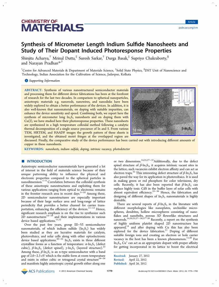
ABSTRACT: Synthesis of various nanostructured semiconductor materialsand processing them for different device fabrications has been at the forefrontof research for the last two decades. In comparison to spherical nanoparticles,anisotropic materials e.g. nanorods, nanowires, and nanodisks have beenwidely explored to obtain a better performance of the devices. In addition, it isalso well-known that nanomaterials, on doping with suitable impurities, canenhance the device sensitivity and speed. Combining both, we report here thesynthesis of micrometer long In2S3 nanosheets and on doping them withCu(I), we have studied here their photoresponse properties. These nanosheetsare synthesized in a high temperature colloidal method following a catalyticthermal decomposition of a single source precursor of In and S. From variousTEM, HRTEM, and HAADF images the growth pattern of these sheets isinvestigated, and the obtained moire fringes at the overlapped region arediscussed. Finally, the comparative study of the device performance has been carried out with introducing different amounts ofcopper in these nanosheets.
KEYWORDS: nanosheets, indium sulfide, doping, intrinsic vacancy, photodetector
■ INTRODUCTIONAnisotropic semiconductor nanomaterials have generated a lotof interest in the field of materials science because of theirunique patterning ability to influence the physical andelectronic properties compared to the spherical particles innanodimension.1−4 Correlation between the colloidal synthesisof these anisotropic nanostructures and exploiting them forvarious applications ranging from optical to electronic remainsin the frontier research area in recent days.5−10 Among these,2D semiconductor nanostructures are especially importantbecause of their large surface area and long-range of latticeperiodicity that provides a better channel for carrier trans-portation, enhancing the efficiency of the devices.11−13 Hence,significant research emphasis is on the rise to synthesize such2D nanostructures14−19 and their implementations in variousdevice based applications.11,12
Over the past few years, group III−VI semiconductornanomaterials, of which indium sulfide (In2S3) has widelybeen studied as they are lucrative materials for catalysis,photovoltaics, and solar cells along with other optoelectronicdevice based applications.20−22 In2S3 exists in three differentcrystalline forms as a function of temperature: α-In2S3 (defectcubic), β-In2S3 (defect spinel), γ-In2S3 (layered structure).23
Among these, β-In2S3 is an n-type semiconductor with a bandgap of 2.0−2.3 eV which is the stable form at room temperatureand exists in either cubic or tetragonal crystal structure24−26
and manifests highly anisotropic crystal growth either along one
or two dimensions.14,25,27−31Additionally, due to the defectspinel structure of β-In2S3, it acquires intrinsic vacant sites inthe lattice; such vacancies exhibit electron affinity and can act aselectron traps.32 This interesting defect structure of β-In2S3 hasalso paved the way for its application in photovoltaics. It is usedin making green or red phosphors for color televisions, drycells. Recently, it has also been reported that β-In2S3 canreplace highly toxic CdS in the buffer layer of solar cells withalmost equivalent efficiency.33−36 Hence, the fabrication anddesigning of different shapes of In2S3 nanomaterials is highlydesirable.There are several reports of β-In2S3 in the literature with
different morphologies like nanoplates, urchinlike micro-spheres, dendrites, hollow microspheres consisting of nano-flakes and nanobelts, porous 3D flowerlike structures andnanorods.14,20,25,27−30,37−39 Recently, a report on the synthesisof highly uniform platelet shaped 2D nanostructure hasappeared,14 and after doping with Cu this has also beenexplored for the device fabrication.11 Doping of differentsuitable foreign ions and creating an electron or hole carriervacancy in the host has been a known phenomenon.11,40 ForIn2S3, Cu
+ can act as an appropriate dopant with proper affinityfor getting incorporated in its lattice to boost the electrical
Received: January 27, 2012Revised: April 22, 2012Published: April 26, 2012
Article
pubs.acs.org/cm
© 2012 American Chemical Society 1779 dx.doi.org/10.1021/cm3003063 | Chem. Mater. 2012, 24, 1779−1785

properties or more specifically device performance.11,41 Hence,in this respect doped 2D In2S3 nanostructures are one of theideal materials. However, for doping, materials with highcrystallinity are required. Hence, it is important to design widearea grown crystalline 2D In2S3 nanomaterials to address theseissues.Exploring the polar organic long chain fatty amines as the
capping agent, solvent, and employing catalytic thermaldecomposition of a single molecular precursor of indium, wereport here the fabrication of two dimensionally grown β-In2S3nanosheets expanding over micrometer length. These sheetsare single crystalline, dispersed in solution, and do not showwrinkling. The crystallinity of these sheets has been supportedwith XRD, HRTEM, and from the obtained moire fringes at theoverlapped regions. Further, a one-pot postdoping strategy hasbeen employed to introduce Cu+ ions into these highlycrystalline sheets, and finally, their photoresponsivity has beenstudied by fabricating a simple thin film based device.
■ EXPERIMENTAL SECTIONMaterials. Indium(III) chloride anhydrous (99.999% - In) (InCl3),
sodium diethyl dithiocarbamate trihydrate (Na-DDTC), octadecyl-amine (ODA, 97%), 1-hexadecylamine (HDA, tech., 90%), elementalsulfur powder (S, 99.98%), indium(III) acetate (99.99%-In) (InAc3),1-octadecene (ODE, tech., 90%), oleylamine (70%), and ITOsubstrates were purchased from Sigma Aldrich. Copper(II) chloridedihydrate crystals (CuCl2·2H2O) were purchased from Merckchemicals. All the chemicals were used without further purification.Preparation of Indium-Tris Diethyldithiocarbamate (In-
DDTC) Precursor. One mmol (0.225 g) of InCl3 and 3 mmol(0.676 g) of Na-DDTC were separately dissolved in methanol andstirred for 10 min to get a clear solution of each. Both of the solutionswere mixed together with constant stirring which resulted in a whiteprecipitate of the desired complex of In-DDTC at room temperature.The precipitate was filtered, washed, and dried for further use insynthesis.Preparation of Cu Stock Solution. 0.5 mmol (0.089 g) of
CuCl2·2H2O was dissolved in 5 mL of oleylamine solution and heatedin inert atmosphere in ambient condition to get a bluish green colorsolution. Reactions were done taking a suitable amount from thisstock.Synthesis of In2S3 Nanosheets. 0.1 mmol (0.056 g) of the In-
DDTC complex was loaded in a three necked flask along with 4 g ofhexadecylamine (HDA) or octadecylamine (ODA). The mixture wasdegassed by purging N2 gas for 15 min to create an inert atmosphere.The temperature was gradually increased to 200 °C, and the solutionturned colloidal. The formation of In2S3 was indicated by theformation of the yellow colloidal solution which was annealed first atthe same temperature for ∼30 min and then at temperature of 300 °Cfor another 2 h. Then the solution was cooled down to roomtemperature, and nanocrystals were purified several times by washingwith acetone and chloroform. Further, all the characterizations havebeen carried out with this purified sample. TEM characterizationrevealed the formation of long-range uniform nanosheets under thisreaction conditions.Synthesis of Cu-Doped In2S3 Nanosheets. For 2% doping of
Cu, 0.04 mL from the Cu stock solution was gradually added to the asprepared solution of In2S3 nanosheets, without any purification of thesheets. The injection spanned over a time period of 15 min. The colorof the solution slowly changed from yellow to red maintaining thecolloidal nature of the reaction medium. In the case of 10% doping, 0.2mL of the Cu stock solution was added following the same methodwhich resulted in a partly clear solution. The temperature for Cuprecursor addition was 220 °C in both cases. After Cu addition in bothcases, the reaction was annealed for 30 min more before cooling itdown to room temperature. Then the product was obtained followingthe usual purification method and characterized further by TEM andXRD measurements.
Fabrication of the Device. To make the photodetectors, first theundoped and doped In2S3 nanocrystals dispersed in toluene (2 mg/mL) were spin coated on precleaned ITO substrates with increasingspeed (from 100 to 1000 rpm) for 40 s. The process of spin coatingwas repeated until the desired thickness ∼1.5 μm measured by DectakStylus 6 M profilometer was obtained. These films were then baked at140 °C for 10 min. Sputter deposited Au electrodes (10 nm) of 1 mmdiameter were made on the top surface of the films and annealed at120 °C for 30 min.
Characterizations. TEM images and EDS spectra were taken on aJEOL-JEM 2010 electron microscopy using a 200 kV electron source.TEM images on STEM (HAADF) were taken on a UHR-FEG-TEM,JEOL; JEM 2100 F model using a 200 kV electron source. Specimenswere prepared by dropping a drop of nanocrystals solution inchloroform on a carbon coated copper grid and the grid was driedunder air. Thermogravimetric analysis (TGA) has been performedwith a TA thermal analysis system at heating rate 10 °C/min under N2environment. XRD of the samples were taken by Bruker D8 Advancepowder diffractometer, using Cu Kα (λ = 1.54 Å) as the incidentradiation. For AFM measurement, a diluted purified sample wasdeposited on a clean mica surface and AFM was measured VEECOdICP -II autoprobe (model AP 0100). The Cu-dopant percentage wasdetermined by ICP-AES using Perkin−Elmer Optima 2100 DVmachine. After removing the unreacted precursors by severe washingswith chloroform and methanol, the purified nanocrystals wereredispersed in chloroform. The chloroform was then evaporated out.Then the dried nanocrystals were digested in concentrated HNO3.The nitric acid solution of the sample was diluted with double distilledwater to carry out the measurement
I−V Measurements. The I−V characteristics between Au andITO electrodes were measured using a Keithley 2400 series sourcemeter. The photocurrents were measured under illumination of 400nm light which was obtained by using a 300 W Xe arc lamp (Oriel)and a monochromator (of model number 74125). The photocurrenttransient responses were recorded by illuminating the sample with 400nm light for 5 s and then switching off the light for another 5 s underthe applied bias of 3 V. All measurements were carried out in ambientcondition.
■ RESULTS AND DISCUSSIONSynthesis and Characterization of 2D In2S3 Nano-
sheets. Single molecular precursor indium-tris diethyldithio-
carbamate (In-DDTC) has been utilized to obtain In2S3 sheets(experimental details provided in the Experimental Section).The thermogravimetric (TG) analysis shows that In-DDTC hasthe decomposition temperature (TD) at 265 °C.42 But it hasbeen observed that the decomposition temperature reduces toas low as 120 °C (Figure S1) in the presence of alkylamine(HDA). This has encouraged us to decompose the precursorsand formation of In2S3 at lower temperature to achieve thecontrol of the anisotropic growth of these nanosheets grownover a large area. TG plots of the In-DDTC complex and onlyHDA has also been provided in the Supporting Information asreference (Figure S2). In a typical synthetic process, when In-DDTC is allowed to decompose at 200 °C in hexadecylamine
Figure 1. Schematic presentation of the synthetic protocol forobtaining organic ligand capped In2S3 nanosheets.
Chemistry of Materials Article
dx.doi.org/10.1021/cm3003063 | Chem. Mater. 2012, 24, 1779−17851780

(HDA) solvent and further annealed at 300 °C, 2D nanosheetsof In2S3 over micrometer length are obtained. The formation ofH2S gas even at 150 °C and the change of the solution color toyellow suggest the decomposition of the single sourcethiocarbamate precursors. The synthetic protocol has beendepicted schematically in Figure 1 (and also Figure S3).Figures 2a, 2b, and 2c (Figure S4) show the TEM images of
single and overlapped sheets. Figure 2d presents the HAADF-
STEM image of overlapped sheets. From these images it hasbeen observed that these sheets are ∼50−200 nm in breadthand lengths in a few micrometers. AFM measurements carriedout on several samples and the obtained height profiles(Supporting Information, Figure S5) suggest that the thicknessof these sheets is within 2 to 3 nm.Further, the detailed crystal structure of the sheets has been
investigated by XRD, SAED, and HRTEM. Figure 3a shows thepowder XRD of these sheets where most of the peak positionsmatch with cubic β-In2S3. For comparison, indexed XRD peaksfrom ICSD no. 202353 are provided in the same figure. SAEDof the sample shown in Figure 3b also supports the cubicstructure where {022} planes having the d-spacing 0.38 nmhave been labeled, but more confirmation of the crystalstructure is obtained from the HRTEM analysis (Figure 3c and3d). From the selected area FFT and inverse FFT of theHRTEM the calculated d-spacing (0.38 nm) suggests that theseare also the {022} planes of cubic β-In2S3.
Moire Patterns in the Overlapped Region of theSheets. As these sheets are crystalline, moire fringes are seenin different overlapped area of the sheets.43 This observationalso further strengthens the high crystallinity of these 2Dnanosheets. Figure 4(a-d) demonstrates the HRTEM imagesobtained from different places showing the moire patterns. Thishas also been observed in the TEM and HAADF images inFigure 2. Close view of Figure 4a and 4b clearly shows thatthese patterns are only obtained from the overlapped areas ofthe sheets. These fringes appear due to the interference of theordered atomic lattice plane of multiple sheets overlapped in aparticular angle as observed in the overlapped area of thesesheets in HRTEM images. To know more about these patternswe have carried out the FFT (inset of Figure 4d) from the
Figure 2. (a, b, and c) Represent the TEM images of as synthesizedIn2S3 nanosheets. (d) Presents the HAADF-STEM image of theoverlapped sheets.
Figure 3. (a) Presents the powder XRD of the nanosheets. The peaks are mostly overlapped with the bulk cubic β-In2S3 (JCPDF 320456). (b)Represents the SAED of the sheets. (c) and (d) Show the HRTEM images obtained from different sheets. Insets top and bottom in (c) and (d) arethe FFT and inverse FFT respectively. The d-spacing of the obtained plane is 0.38 nm, and the planes are intersecting each other at 120 degrees.Hence these planes are {022} planes and the viewing axis is [111].
Chemistry of Materials Article
dx.doi.org/10.1021/cm3003063 | Chem. Mater. 2012, 24, 1779−17851781

overlapped areas which indicate the presence of two planes. Formore clarity, inverse FFT has been analyzed which shows thewell resolved moire fringes (Figure 4e) generated due to the(022) planes of two different In2S3 sheets overlapped with anangle of 7 degrees as shown in Figure 4f. A schematicpresentation of two such atomic planes and the obtained moire patterns in the overlapped region are shown in Figure 4g.Mechanism of the Formation of Nanosheets. System-
atic analysis of the reaction progress reveals that the reactionmedium is very much pivotal. It has been observed that thelong-range growth of these nanosheets mostly occurs in fattyamine solvent. When it is diluted with an optimum amount(>20% by weight) of noncoordinating solvent like 1-octadecene(ODE), mostly rolled sheets or flakes are obtained (Figure S6)rather than the free-standing sheets obtained in pure aminesolvent. Amines help in the decomposition of the precursorsand act as capping ligands dispersing the nanosheets into thesolution. An insufficient amount of these amines mostly affectthe growth pattern or break the long sheets into fragments dueto long time annealing that lead to rolled sheet or flakes likestructures. Further, instead of the single source precursor, whendifferent sources for indium and sulfur like In-carboxylates andelemental S respectively are used in alkyl amine, similarirregular nanostructures are observed (Figure S7). This provesthat the morphology of these nanostructures remains under thecontrol of solvent polarity, nature of the ligands (coordinating/noncoordinating), and molecular precursors though the growthis always anisotropic irrespective of all the conditions. But for
the free-standing 2D sheets, the reaction needs to be carriedout in pure fatty amine solvent.Further, to understand the formation of these crystalline 2D
nanosheets, intermediate samples were investigated. Interest-ingly, all the collected samples within 250 °C using HDA as thesolvent are found to be amorphous in nature. TEM images ofthe samples collected at 200 °C are shown in Figure S8. Asthese are amorphous, their growth pattern could not beconfirmed, but these amorphous structures are confirmed to beIn2S3 by EDS analysis (Figure S9) which shows the In:Sstoichiometric ratio of ∼1:1.5. This indicates that thesestructures are indium sulfide and not the unreacted precursors.This means the single source precursors decompose at lowtemperature (∼150 °C) in the presence of amine and lead toformation of amorphous In2S3 structures which on annealing athigher temperature (∼300 °C) slowly convert into crystalline2D nanosheets. This transformation has been observed as aslow process and needs sufficient annealing time. When thenucleation for the crystalline sheets begins, the existingamorphous In2S3 in solution supply the monomers andfacilitate the sheets to grow in the allowed 2D direction. As aresult, highly crystalline β-In2S3 nanosheets are formed.
Doping of Cu in the Sheets. These sheets are furtherexplored by doping with copper and the subsequent opto-electrical transport properties measurements. We surprisinglyfound that introduction of up to 2% of Cu during the synthesisdoes not affect the shape and phase of the crystal and improvesthe speed of the photoresponse immensely. To study this, we
Figure 4. (a) and (b) Show the TEM images of overlapped sheets showing moire patterns on the overlapping region. (c) and (d) Show the HRTEMimages from different overlapped regions. Insert of (d) is the selected area FFT of the HRTEM image in (d). (e) Presents the inverse FFT obtainedafter masking the spots in the FFT of the inset of (d). (f) Represents the inverse FFT considering the (022) planes of the FFT of the insert in (d).(g) Shows the schematic model of two sheets placed at an angle of 7 degrees and their overlap. The atomic placements are determined consideringthe cubic structure of In2S3. Insets blue and green images represent the inverse FFT of blue and green masked in the FFT (inset of f).
Chemistry of Materials Article
dx.doi.org/10.1021/cm3003063 | Chem. Mater. 2012, 24, 1779−17851782

have fabricated a very simple device by putting a thin film of theundoped (and doped) materials on ITO and making an Auelectrode on the film (details in the Experimental Section). TheSEM image of the film has been provided in the SupportingInformation (Figure S10). Here, we have adopted a facile one-pot postdoping strategy to dope Cu(I) into the nanosheets.First, In2S3 nanosheets are synthesized and without any furtherpurification, CuCl2 dissolved in oleylamine is added into theIn2S3 solution dropwise. An optimum concentration of thedopant Cu, which is 2% of the concentration of In precursor ischosen to be incorporated into the sheets that is low enough tofacilitate insertion of Cu ions retaining the original sheetstructure of the undoped In2S3 nanosheets as observed from theTEM image (Figure S11). We have also doped a higher amountof Cu (∼10%) into the sheet. In this case, overdoping partlydestroys the integrity of the nanosheets as shown in Figure S12.In order to ascertain the incorporation of Cu dopant ions intothe In2S3 sheet, we carried out ICP-AES measurements, and thecopper amounts of 1.7% and 9.2% have been detected in boththe samples respectively indicating the incorporation of copperinto final products. The oxidation state of Cu in such cases ofdoping has been under debate for a long time until a fewresearch reports threw light on them and showed that even ifthe Cu2+ precursor is used as dopant, it reduces to the Cu+ statein the presence of amine and gets incorporated in the +1 state
into the host lattice.11 We have further performed powder XRDon the optimized Cu (2%) doped sample. The obtained XRDpattern remains similar to the undoped sheets. This suggeststhat other copper compounds such as CuO or Cu2S are notobtained as the side products. Hence, we can assume here thatthe Cu+ ions are incorporated into the sheet structure ratherthan forming any separate phase.
Study of Photoresponse Properties of Undoped andDoped Sheets. In Figure 5 we report the I−V characteristics(left panel) and temporal photoresponse (right panel) for thephotodetectors made from the doped and undoped In2S3nanosheets in the dark as well as under light illuminationcondition. The linear I−V curves confirm the Ohmic nature ofthe contacts for all the samples. Under illuminated condition, atall bias voltages, the current conduction is more compared tothat under dark condition. As shown in Table 1, thephotocurrent gain (IPhoton /Idark) in undoped In2S3 is 155,while the value is 186 for 2% Cu doping as calculated from thegrowth-decay curves in the right panel of Figure 5. By 2% Cudoping there is no significant change in the dark as well asphotocurrents, and thus the gain remains almost in a similarorder but with a slight increase in the magnitude. However, thevalue significantly decreases for the 10% doping case. This ispossibly due to the creation of excess defects in the crystallattice by Cu incorporation which act as the traps for the
Figure 5. Left Panel: I−V plots for undoped (a), 2% Cu-doped (b), and 10% Cu doped (c) In2S3 nanosheet films under dark and 400 nmmonochromatic light illuminations. Right Panel: Temporal photoresponse for undoped (d), 2% Cu doped (e), and 10% Cu-doped (f) In2S3nanosheets. The upward arrow (↑) and downward arrow (↓) represent the switching on and off step of the illumination respectively.
Table 1. Summary of Device Performance as a Function of Extent of Cu Doping
amount ofCu (mole %)
dark current(Amp)
photocurrent(Amp)
gain(Iphoton/Idark)
growth time(∼90%)
decay time(∼90%)
0 3.94 × 10 −6 6.12 × 10 −4 155 2.0 s 0.1 s2 3.91 × 10 −6 7.29 × 10 −4 186 0.2 s 0.2 s10 3.42 × 10 −7 5.42 × 10 −6 16 0.1 s 0.1 s
Chemistry of Materials Article
dx.doi.org/10.1021/cm3003063 | Chem. Mater. 2012, 24, 1779−17851783
carriers.44 Due to formation of trap states, the current decreasesin 10% doping sample.45 Here, it is important to note thatincorporation of excess Cu in In2S3 indeed enhances the trap ordefect states and dismantles the nanosheets to irregularlyshaped nanostructures. The photodetector made from this Cu-doped In2S3 (10% Cu) with an identical absorbance value asthat of the undoped and 2% doped sheets and prepared undersimilar reaction conditions shows degraded performance: a lowgain value. This can be probably attributed to the chances thatthe excessive concentration of Cu+ can cause competition toIn3+ for S ions and thus deforming the sheet structure anddegrading the overall device performance. A dramatic improve-ment in the photoresponse time (for 90% growth ofphotocurrent) has been noticed with doped samples. Anorder of magnitude decrease in the growth time has beenobserved in the case of both 2% and 10% Cu doping (Table 1)samples. The decay time (90% decay in the current) for allthree samples however remains in the similar order ofmagnitude as shown in Table 1. The doping of Cu ions inthe vacancies of defect spinel structure of In2S3 leads to asignificant increase in the response time and consequentlyboosts the device speed. We can predict from literature, Cu+
doping narrows the band gap of In2S3 and decreases thedistance between valence band-edge of the host and traps.11
Thus, we consider this as the reason for such an enhancementof the photoresponse speed which widens the opportunity ofexploiting Cd or Pb free nanosheet structures for device basedapplications.
■ CONCLUSION
In summary, an efficient high temperature colloidal techniquehas been developed to synthesize single crystalline In2S3nanosheets by decomposition of a single source In-DDTCprecursor in fatty amine. Initially amorphous nanostructureswith irregular shapes are formed, and on annealing at highertemperature these are transformed to 2D crystalline nano-sheets. These amine capped nanosheets are observed free-standing, wrinkle free, and dispersed in solution. Furthermore,Cu has been incorporated into the In2S3 nanosheets varying itsamount (0−10%) in the In2S3 nanosheets via a postdopingtechnique. Finally, comparative optoelectronic studies havebeen carried out, and it has been found that the In2S3nanosheet is one of the most desirable materials among themetal sulfides to be implemented in photodetector and furtherenhancement of the photoresponse properties by 2% of Cudoping and has a better prospect in device applications.
■ ASSOCIATED CONTENT
*S Supporting InformationTG plots of HDA, In-DDTC, In-DDTC in HDA, digitalscheme, EDS, TEM images. This material is available free ofcharge via the Internet at http://pubs.acs.org.
■ AUTHOR INFORMATION
Corresponding Author*E-mail: [email protected].
NotesThe authors declare no competing financial interest.
■ ACKNOWLEDGMENTS
DST and CSIR of India are acknowledged for funding. S.A. andS.S. acknowledge CSIR, India for a fellowship. N.P. thanks LNJBhilwara for a fellowship.
■ REFERENCES(1) Hu, J.; Odom, T. W.; Lieber, C. M. Acc. Chem. Res. 1999, 32,435−445.(2) Wang, C.; Hu, Y.; Lieber, C. M.; Sun, S. J. Am. Chem. Soc. 2008,130, 8902−8903.(3) Hu, J.; Li, L.-s.; Yang, W.; Manna, L.; Wang, L.-w.; Alivisatos, A.P. Science 2001, 292, 2060−2063.(4) Acharya, S.; Panda, A. B.; Efrima, S.; Golan, Y. Adv. Mater. 2007,19, 1105−1108.(5) Peng, X.; Manna, U.; Yang, W.; Wickham, J.; Scher, E.;Kadavanich, A.; Alivisatos, A. P. Nature 2000, 404, 59−61.(6) Fu, A.; Gu, W.; Boussert, B.; Koski, K.; Gerion, D.; Manna, L.; LeGros, M.; Larabell, C. A.; Alivisatos, A. P. Nano Lett. 2007, 7, 179−182.(7) Kang, S. H.; Choi, S.-H.; Kang, M.-S.; Kim, J.-Y.; Kim, H.-S.;Hyeon, T.; Sung, Y.-E. Adv. Mater. 2008, 20, 54−58.(8) Amirav, L.; Alivisatos, A. P. J. Phys. Chem. Lett. 2010, 1, 1051−1054.(9) Li, L.-S.; Walda, J.; Manna, L.; Alivisatos, A. P. Nano Lett. 2002, 2,557−560.(10) Wang, J.-J.; Cao, F.-F.; Jiang, L.; Guo, Y.-G.; Hu, W. - P.; Wan,L.-J. J. Am. Chem. Soc. 2009, 131, 15602−15603.(11) Tang, J.; Konstantatos, G.; Hinds, S.; Myrskog, S.; Pattantyus-Abraham, A. G.; Clifford, J.; Sargent, E. H. ACS Nano 2009, 3, 331−338.(12) Vaughn, D. D., II; Patel, R. J.; Hickner, M. A.; Schaak, R. E. J.Am. Chem. Soc. 2010, 132, 15170−15172.(13) Lee, K. H.; Shin, H.-J.; Lee, J.; Lee, I.-y.; Kim, G.-H.; Choi, J.-Y.;Kim, S.-W. Nano Lett. 2012, 12, 714−718.(14) Park, K. H.; Jang, K.; Son, S. U. Angew. Chem., Int. Ed. 2006, 45,4608−4612.(15) Tang, Z.; Zhang, Z.; Wang, W.; Glotzer, S. C.; Kotov, N. A.Science 2006, 314, 274−278.(16) Ithurria, S.; Dubertret, B. J. Am. Chem. Soc. 2008, 130, 16504−16505.(17) Jang, J.-t.; Jeong, S.; Seo, J.-w.; Kim, M.-C.; Sim, E.; Oh, Y.;Nam, S.; Park, B.; Cheon, J. J. Am. Chem. Soc. 2011, 133, 7636−7639.(18) Li, Z.; Peng, X. J. Am. Chem. Soc. 2011, 133, 6578−6586.(19) Son, J. S.; Wen, X.-D.; Joo, J.; Chae, J.; Baek, S.-i.; Park, K.; Kim,J. H.; An, K.; Yu, J. H.; Kwon, S. G.; Choi, S.-H.; Wang, Z.; Kim, Y.-W.; Kuk, Y.; Hoffmann, R.; Hyeon, T. Angew. Chem., Int. Ed. 2009, 48,6861−6864.(20) Du, W.; Zhu, J.; Li, S.; Qian, X. Cryst. Growth. Des. 2008, 8,2130−2136.(21) Liu, Y.; Xu, H.; Qian, Y. Cryst. Growth. Des. 2006, 6, 1304−1307.(22) Fu, X.; Wang, X.; Chen, Z.; Zhang, Z.; Li, Z.; Leung, D. Y. C.;Wu, L.; Fu, X. Appl. Catal., B 2010, 95, 393−399.(23) Yu, S.-H.; Shu, L.; Wu, Y.-S.; Yang, J.; Xie, Y.; Qian, Y.-T. J. Am.Ceram. Soc. 1999, 82, 457−460.(24) Asikainen, T.; Ritala, M.; Leskela, M. Appl. Surf. Sci. 1994, 82/83, 122−125.(25) Franzman, M. A.; Brutchey, R. L. Chem. Mater. 2009, 21, 1790−1792.(26) Avivi (Levi), S. P.; Palchik, O.; Palchik, V.; Slifkin, M. A.; Weiss,A. M.; Gedanken, A. Chem. Mater. 2001, 13, 2195−2200.(27) Kim, Y. H.; Lee, J. H.; Shin, D.-W.; Park, S. M.; Moon, J. S.;Nam, J. G.; Yoo, J.-B. Chem. Commun. 2010, 46, 2292−2294.(28) Xiong, Y.; Xie, Y.; Du, G.; Tian, X.; Qian, Y. J. Solid State Chem.2002, 166, 336−340.(29) Zhu, H.; Wang, X.; Yang, W.; Yang, F.; Yang, X. Mater. Res. Bull.2009, 44, 2033−2039.
Chemistry of Materials Article
dx.doi.org/10.1021/cm3003063 | Chem. Mater. 2012, 24, 1779−17851784

(30) Chen, L.-Y.; Zang, Z.-D.; Wang, W.-Z. J. Phys. Chem. C. 2008,112, 4117−4123.(31) Xing, Y.; Zhang, H.; Song, S.; Feng, J.; Lei, Y.; Zhao, L.; Li, M.Chem. Commun. 2008, 44, 1476−1478.(32) Jayakrishnan, R. J.; John, T. T.; Kartha, C. S.; Vijayakumar, K.P.; Jain, D.; Chandra, L. S. S.; Ganesan, V. J . Appl. Phys. 2008, 103, 1−6.(33) Dalas, E.; Kobotiatis, L. J. Mater. Sci. 1993, 28, 6595−6597.(34) Naghavi, N.; Spiering, S.; Powalla, M.; Cavana, B.; Lincot, D.Prog. Photovoltaics 2003, 11, 437−443.(35) Sterner, J.; Malmstrom, J.; Stolt, L. Prog. Photovoltaics 2005, 13,179−193.(36) Braunger, D.; Hariskos, D.; Walter, T.; Schock, H. W. Sol.Energy Mater. Sol. Cells 1996, 40, 97−102.(37) Liu, L.; Liu, H.; Kou, H. -Z.; Wang, Y.; Zhou, Z.; Ren, M.; Ge,M.; He, X. Cryst. Growth. Des. 2009, 9, 113−117.(38) Liu, Y.; Zhang, M.; Gao, Y.; Zhang, R.; Qian, Y. Mater. Chem.Phys. 2007, 101, 362−366.(39) Wang, W.; Zhu, W.; Zhang, L. Res. Chem. Intermed. 2009, 35,761−767.(40) Noone, K. M.; Ginger, D. S. ACS Nano 2009, 3, 261−265.(41) Rehwald, W.; Harbeke, G. J. Phys. Chem. Solid 1965, 26, 1309−1318.(42) Oliveira, M. M.; Pessoa, G. M.; Carvalho, L. C.; Peppe, C.;Souza, A. G.; Airoldi, C. Thermochim. Acta 1999, 328, 223−230.(43) Soejima, T.; Kimizuka, N. Chem. Lett. 2005, 34, 1234−1235.(44) Ghosh, T.; Dutta, M.; Mridha, S.; Basak, D. J. Electrochem. Soc.2009, 156, H285−H289.(45) Konstantatos, G.; Levina, L.; Fischer, A.; Sargent, E. H. NanoLett. 2008, 8, 1446−1450.
Chemistry of Materials Article
dx.doi.org/10.1021/cm3003063 | Chem. Mater. 2012, 24, 1779−17851785


![Dopant Diffusion – physics [Repaired]](https://img.dokumen.tips/doc/110x75/577d20d41a28ab4e1e93db83/dopant-diffusion-physics-repaired.jpg)