Embed Size (px)
Citation preview
SYNTHESIS AND MODELING OF RF INTEGRATED PLANAR SPIRAL
INDUCTOR
SEE GUAN HUEI
A thesis submitted in fulfillment of the
requirements for the award of the degree of
Master of Engineering (Electrical)
Fakulti Kejuruteraan Elektrik
Universiti Teknologi Malaysia
JULY, 2004

iii
To my beloved parents, and Savior Jesus Christ.

iv
ACKNOWLEDGEMENT
I would like to take this very best opportunity to acknowledge the help and
support from various people that have contributed to the success of this research
work.They are my supervisors, PM Dr. Mazlina Esa and Mr. Albert V Kordesch.
Many thanks to them, I can’t really put it into words how much my gratitude is to
them for their guidance, attention, etc…Well I must say, they are more than just
supervisor, but also friends.
I would not also forget fellow colleagues in the Device Modeling group, Soon
Aik, Philip, Razman, Yusman, Hafizah and Fahmi. It was fun working together with
all of you. Thanks for making it a memorable stay in Silterra. I’m also in debt to the
person in charge of this postgraduate program at Silterra, Lena Tan, and thanks for
fighting for our benefits while I was in the company.
Besides that, special thanks also to Michelle for assisting my work in
literature search; My University’s friends, Davy who shared his room while I was
there at UTM, Skudai; SILTERRA MALAYSIA SDN BHD for providing the
avenue and financial assistance for this research; ARFIC for providing technical
support and characterization of the inductors.
And of course, I’m eternally grateful for God that has been with me all this
while!

v
ABSTRACT
The recent development of the wireless market has increased the interest in
the integrated inductor for Radio Frequency Integrated Chip (RFIC) applications.
Though Electromagnetic (EM) simulation is available, it is usually expensive, slow
and difficult to integrate into the RFIC design flow. Therefore, the alternative option
of a generic, simple yet accurate procedure to design the inductor is very desirable.
Based on the physical model, an integrated inductor synthesis procedure has been
developed and implemented in Microsoft EXCEL. This synthesis tool is able to
identify the maximum quality factor (Q) at the operating frequency (e.g. 1.8 GHz for
mobile communication, 2.45 GHz for wireless Local Area Network (LAN)) of the
desired inductor very quickly. An example of synthesizing a 3 nH inductor is
demonstrated using this tool. Besides that, another type of integrated inductor model
known as extracted model is also needed for circuit simulation. An improved model
extraction procedure has been proposed in this research and has been embedded in
another EXCEL file. This new procedure has reduced the number of terms required
and proved to be more accurate even in the region beyond the Self-Resonant
Frequency (SRF). The above two types of integrated inductor modeling were then
“combined” into a new global integrated inductor model in SPICE, which is a
compromise of accuracy (extracted model) and scalability (physical model). This
model is accurate up to ~2 GHz, within an average error of 10 %. Using this new
model, one can have the freedom to choose the value of inductance and more
flexibility in circuit design. In addition, the layout optimization and circuit
optimization can be done using the same model thus saving time and reducing cost.
This is a novel integrated type of model that has never been published in any other
research.
vi
ABSTRAK
Perkembangan terkini pasaran tanpa wayar telah meningkatkan minat
terhadap induktor bersepadu untuk aplikasi litar bersepadu frekuensi radio (RFIC).
Walaupun tedapat simulasi elektromagnet (EM), ini biasanya mahal, lambat dan
susah diimplementasi dalam aliran rekabentuk RFIC. Oleh itu, pilihan alternatif
tatacara tepat yang generik tetapi mudah sangat diperlukan. Tatacara sintesis
induktor bersepadu berasaskan model fizikal telah dibangunkan dan diimplemen
menggunakan EXCEL. Alatan sintesis ini berupaya menentukan faktor kualiti (Q)
optimum dengan pantas pada frekuensi operasinya (seperti 1.8 GHz untuk
telekomunikasi bergerak dan 2.45 GHz untuk rangkaian kawasan tempatan (LAN)
tanpa wayar). Satu contoh untuk sintesis induktor 3 nH ditunjukkan menggunakan
alatan ini. Selain itu, model induktor bersepadu yang dikenali sebagai model
terekstrak juga dibangunkan untuk simulasi litar. Tatacara pengekstrakan model yang
telah diperbaiki dicadangkan dalam kajian ini dan dimasukkan ke dalam satu lagi fail
EXCEL. Tatacara baru ini telah berjaya mengurangkan beberapa sebutan dan
terbukti lebih tepat walaupun dalam julat frekuensi selepas frekuensi resonan diri
(SRF). Kedua-dua jenis model induktor ini telah “digabung” untuk menghasilkan
model induktor global dalam bentuk SPICE, yang merupakan krompomi di antara
ketepatan (model terekstrak) dan kebolehskalaan (model fizikal). Model ini
mempunyai ralat dalam lingkungan 10 %, tepat sehingga ~2.0 GHz. Dengan
menggunakan model baru ini, seseorang boleh mengawal nilai induktan yang
memberikan fleksibiliti rekabentuk litar. Tambahan pula, pengoptimuman bentangan
dan pengoptimuman litar boleh dilakukan dengan model yang sama, seterusnya dapat
menjimatkan masa dan mengurangkan kosnya. Ini merupakan model bersepadu baru
yang belum pernah dilaporkan dalam kajian lain

vii
TABLE OF CONTENTS
TITLES PAGE
ACKNOWLEDGEMENT........................................................................................ iv
ABSTRACT................................................................................................................ v
ABSTRAK ................................................................................................................. vi
TABLE OF CONTENTS.........................................................................................vii
LIST OF TABLES ..................................................................................................... x
LIST OF FIGURES .................................................................................................. xi
LIST OF ABBREVIATIONS ................................................................................ xiv
LIST OF SYMBOLS .............................................................................................. xvi
LIST OF APPENDIXES ......................................................................................... xx
INTRODUCTION...................................................................................................... 1
1.1. Research Background .................................................................................... 2
a.) Inductor’s Application In RF Design............................................................. 2
b.) Inductor On Silicon........................................................................................ 5
1.2 Objectives and scopes of research ................................................................. 9
1.3 Thesis Organization ....................................................................................... 9
LITERATURE REVIEW AND PREVIOUS WORKS........................................ 11
2.1 The Importance of Inductor Q ..................................................................... 12
2.2 The Current and Future Trend Toward CMOS ............................................ 13
2.3 Inductance Calculations and Inductor Modeling ......................................... 15
2.4 Model Extraction ......................................................................................... 19
2.5 Q definitions................................................................................................. 20
2.6 Q Improvements........................................................................................... 21
2.7 Inductor Design and Optimization............................................................... 23
PHYSICAL MODELING AND INDUCTOR SYNTHESIS ............................... 25
3.1 Physical Modeling ....................................................................................... 28
viii
3.1.1 Calculation of Series Inductance, Ls ............................................................ 29
(a) Greenhouse’s Inductance Expression, LGMD2 [Tuan, 2000] .............................. 30
(b) Mohan’s Modified Wheeler Inductance Expression, Lmwhe [Mohan, et al., 1999]
...................................................................................................................... 31
(c) Mohan’s Current Sheet Inductance Approximation, Lgmd [Mohan, et al., 1999]..
...................................................................................................................... 32
(d) Mohan’s Monomial Data Fit Inductance Expression [Mohan, et al., 1999]..... 32
(e) Jenei’s Physics Based Closed Form Inductance Expression [Jenei, et al.
(2000,2002)] ........................................................................................................... 33
(f) Asgaran’s New Physics Based Closed Form Inductance Expression [Asgaran,
2002] ...................................................................................................................... 34
(i) Self Inductance............................................................................................ 46
(ii) Negative Mutual Inductance ....................................................................... 48
(iii) Positive Mutual Inductance......................................................................... 49
3.1.2 Series Capacitance, Cs.................................................................................. 50
3.1.3 Series Resistance, Rs .................................................................................... 51
3.1.4 Substrate Parasitics ...................................................................................... 52
3.2 Inductor Synthesis........................................................................................ 52
3.2.1 Q Definition ................................................................................................. 53
3.2.2 L curve ......................................................................................................... 58
3.3 Integrated Inductor Synthesis Example ....................................................... 65
3.4 Summary ...................................................................................................... 67
INTEGRATED INDUCTOR MACRO MODEL EXTRACTION,
OPTIMIZATION AND WIDE-BAND MODELING........................................... 69
4.1 High Frequency On-wafer Measurement Technique................................... 70
4.2 Integrated Inductor Macro Model Extraction .............................................. 72
4.3 Model Optimization ..................................................................................... 84
4.4 Wide Band Inductor Modeling .................................................................... 86
4.5 Summary ...................................................................................................... 91
GLOBAL INTEGRATED INDUCTOR MODEL................................................ 93
5.1 Global Integrated Inductor Model Development......................................... 94
5.2 GIIM Verification and Validation.............................................................. 101
5.3 Summary .................................................................................................... 110
CONCLUSIONS AND RECOMMENDATIONS............................................... 111

ix
6.1 Conclusions................................................................................................ 111
6.2 Recommendations...................................................................................... 113
(a) On-Chip Transformers and Baluns ............................................................ 113
(b) Integrated Capacitor and Resistor Modeling ............................................. 114
(c) Circuit Implementation Using the Inductor Model.................................... 114
REFERENCES....................................................................................................... 115
APPENDIX A: Two port networks ...................................................................... 123
APPENDIX B: Integrated Spiral Inductor Layout View ..................................... 126
APPENDIX C: Integrated Spiral Inductor Synthesis Using EXCEL................... 128
APPENDIX D:Integrated Spiral Inductor Macro Model Extraction and
Optimization Using EXCEL................................................................................. 131
APPENDIX E: PSPICE Format of Global Integrated Inductor Model ................ 134
APPENDIX F: List of Publications...................................................................... 135
x
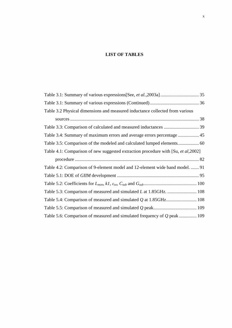
LIST OF TABLES
Table 3.1: Summary of various expressions[See, et al.,2003a] ................................. 35
Table 3.1: Summary of various expressions (Continued).......................................... 36
Table 3.2 Physical dimensions and measured inductance collected from various
sources .............................................................................................................. 38
Table 3.3: Comparison of calculated and measured inductances .............................. 39
Table 3.4: Summary of maximum errors and average errors percentage .................. 45
Table 3.5: Comparison of the modeled and calculated lumped elements.................. 60
Table 4.1: Comparison of new suggested extraction procedure with [Su, et al,2002]
procedure .......................................................................................................... 82
Table 4.2: Comparison of 9-element model and 12-element wide band model. ....... 91
Table 5.1: DOE of GIIM development ...................................................................... 95
Table 5.2: Coefficients for Lmon, k1, εox, Csub and Gsub ............................................. 100
Table 5.3: Comparison of measured and simulated L at 1.85GHz. ......................... 108
Table 5.4: Comparison of measured and simulated Q at 1.85GHz.......................... 108
Table 5.5: Comparison of measured and simulated Q peak..................................... 109
Table 5.6: Comparison of measured and simulated frequency of Q peak ............... 109
xi
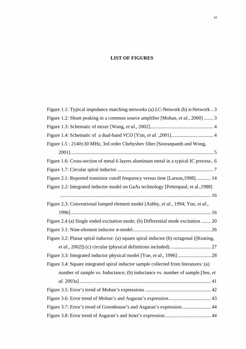
LIST OF FIGURES
Figure 1.1: Typical impedance matching networks (a) LC-Network (b) π-Network .. 3
Figure 1.2: Shunt peaking in a common source amplifier [Mohan, et al., 2000] ........ 3
Figure 1.3: Schematic of mixer [Wang, et al., 2002]................................................... 4
Figure 1.4: Schematic of a dual-band VCO [Yim, et al. ,2001].................................. 4
Figure 1.5 : 2140±30 MHz, 3rd order Chebyshev filter [Sooranpanth and Wong,
2001]. .................................................................................................................. 5
Figure 1.6: Cross-section of metal 6 layers aluminum metal in a typical IC process.. 6
Figure 1.7: Circular spiral inductor.............................................................................. 7
Figure 2.1: Reported transistor cutoff frequency versus time [Larson,1998]. ........... 14
Figure 2.2: Integrated inductor model on GaAs technology [Pettenpaul, et al.,1988]
.......................................................................................................................... 16
Figure 2.3: Conventional lumped element model [Ashby, et al., 1994; Yue, et al.,
1996] ................................................................................................................. 16
Figure 2.4 (a) Single ended excitation mode; (b) Differential mode excitation ........ 20
Figure 3.1: Nine-element inductor π-model............................................................... 26
Figure 3.2: Planar spiral inductor: (a) square spiral inductor (b) octagonal ([Keating,
et al., 2002]) (c) circular (physical definitions included). ................................ 27
Figure 3.3: Integrated inductor physical model [Yue, et al., 1996] ........................... 28
Figure 3.4: Square integrated spiral inductor sample collected from literatures: (a)
number of sample vs. Inductance; (b) inductance vs. number of sample.[See, et
al. 2003a] .......................................................................................................... 41
Figure 3.5: Error’s trend of Mohan’s expressions ..................................................... 42
Figure 3.6: Error trend of Mohan’s and Asgaran’s expression.................................. 43
Figure 3.7: Error’s trend of Greenhouse’s and Asgaran’s expression ....................... 44
Figure 3.8: Error trend of Asgaran’s and Jenei’s expression ..................................... 44
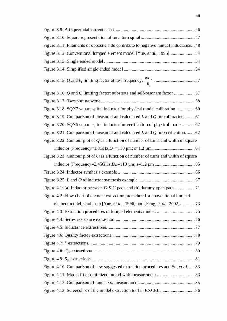
xii
Figure 3.9: A trapezoidal current sheet ...................................................................... 46
Figure 3.10: Square representation of an n turn spiral ............................................... 47
Figure 3.11: Filaments of opposite side contribute to negative mutual inductance... 48
Figure 3.12: Conventional lumped element model [Yue, et al., 1996]...................... 54
Figure 3.13: Single ended model ............................................................................... 54
Figure 3.14: Simplified single ended model .............................................................. 54
Figure 3.15: Q and Q limiting factor at low frequency, s
s
RLω
. .................................. 57
Figure 3.16: Q and Q limiting factor: substrate and self-resonant factor .................. 57
Figure 3.17: Two port network .................................................................................. 58
Figure 3.18: SQN7 square spiral inductor for physical model calibration ................ 60
Figure 3.19: Comparison of measured and calculated L and Q for calibration. ........ 61
Figure 3.20: SQN5 square spiral inductor for verification of physical model........... 62
Figure 3.21: Comparison of measured and calculated L and Q for verification. ....... 62
Figure 3.22: Contour plot of Q as a function of number of turns and width of square
inductor (Frequency=1.8GHz,D =110 µm; s=1.2 µmin ..................................... 64
Figure 3.23: Contour plot of Q as a function of number of turns and width of square
inductor (Frequency=2.45GHz,D =110 µm; s=1.2 µmin ................................... 65
Figure 3.24: Inductor synthesis example ................................................................... 66
Figure 3.25: L and Q of inductor synthesis example ................................................. 67
Figure 4.1: (a) Inductor between G-S-G pads and (b) dummy open pads ................. 71
Figure 4.2: Flow chart of element extraction procedure for conventional lumped
element model, similar to [Yue, et al., 1996] and [Feng, et al., 2002]............. 73
Figure 4.3: Extraction procedures of lumped elements model. ................................. 75
Figure 4.4: Series resistance extraction...................................................................... 76
Figure 4.5: Inductance extractions. ............................................................................ 77
Figure 4.6: Quality factor extractions. ....................................................................... 78
Figure 4.7: f extractions.r ........................................................................................... 79
Figure 4.8: C extractions.ox ........................................................................................ 80
Figure 4.9: R extractionssi .......................................................................................... 81
Figure 4.10: Comparison of new suggested extraction procedures and Su, et al. ..... 83
Figure 4.11: Model fit of optimized model with measurement ................................. 83
Figure 4.12: Comparison of model vs. measurement. ............................................... 85
Figure 4.13: Screenshot of the model extraction tool in EXCEL .............................. 86

xiii
Figure 4.14: Wide band equivalent circuit [Melendy et al., 2002] ............................ 88
Figure 4.15: Simplified equivalent circuit. ................................................................ 89
Figure 4.16: Comparison of model fits for Q............................................................. 90
Figure 4.17: Comparison of model fits for L ............................................................. 90
Figure 5.1: Circular spiral inductor with 6.5 turns..................................................... 95
Figure 5.2: Single ended inductor model in GIIM ..................................................... 97
Figure 5.3: Comparison of Monomial Data Fit with measured inductance data ....... 98
Figure 5.4: Test of scalability for monomial data fit for circular inductor ................ 99
Figure 5.5: Simulated L and Q of w10r75n3 inductor ............................................. 102
Figure 5.6: Simulated L and Q of w10r75n4 inductor ............................................. 103
Figure 5.7: Simulated L and Q of w10r75n5 inductor ............................................. 103
Figure 5.8: Simulated L and Q of w10r75n6 inductor ............................................. 104
Figure 5.9: Simulated L and Q of w10r75n7 inductor ............................................. 104
Figure 5.10: Simulated L and Q of w10r75n8 inductor ........................................... 105
Figure 5.11: Simulated L and Q of w10r125n2 inductor ......................................... 105
Figure 5.12: Simulated L and Q of w10r125n3 inductor ......................................... 106
Figure 5.13: Simulated L and Q of w10r125n4 inductor ......................................... 106
Figure 5.14: Simulated L and Q of w10r125n5 inductor ......................................... 107
Figure 5.15: Simulated L and Q of w10r125n6 inductor ......................................... 107

xiv
LIST OF ABBREVIATIONS
A : Ampere
Al : Aluminum
ASITIC : Analysis and Simulation of Spiral Inductor and Transformer
for ICs
BPF : Band bass filter
CMOS : Complementary metal oxide silicon
DC : Direct current
DOE : design of experiment
EM : Electromagnetic
F : Farad
fmax : Maximum frequency
ft : Cut-off frequency
GaAs : Gallium arsenide
GHz : Giga-hertz
GIIM : Global integrated inductor model
GMD : geometric mean distance
G-S-G : Ground-signal-ground probe pad
H : Henry
Hz : Hertz
IC : Integrated circuit
IP3 : 3rd order intercept point
LC : Inductor, Capacitor
LNA : Low noise amplifier
LPF : Low pass filter
LRRM : Line-Reflect (open)-Reflect (short)-Match
LTCC : Low temperature co-fired ceramic
MOS : Metal on silicon

xv
nH : Nano-Henry
PEEC : Partial element equivalent circuit
RF : Radio frequency
RFIC : Radio frequency Integrated Circuit
Si : Silicon
SISP : Spiral Inductor Simulation Tool
S-parameter : Scattering parameter
SPICE : General purpose circuit simulation program
SRF : Self-resonant frequency
VCO : Voltage controlled oscillator
vs. : Versus
Wb : Weber
µm : Micro-meter

xvi
LIST OF SYMBOLS
A : Voltage ratio when port 2 is open;
a : 1st dimension of a rectangular in Greenhouse expression
a1 : Incident electromagnetic waves at port 1
a2 : Incident electromagnetic waves at port 2
B : Transfer impedance when port 2 is short-circuited;
b : 2nd dimension of a rectangular in Greenhouse expression
b1 : Reflected electromagnetic waves at port 1
b2 : Reflected electromagnetic waves at port 2
C : Transfer admittance when port 2 is open;
C1 : Mohan’s current sheet approximation 1st layout dependent coefficient
C2 : Mohan’s current sheet approximation 2nd layout dependent coefficient
C3 : Mohan’s current sheet approximation 3rd layout dependent coefficient
C4 : Mohan’s current sheet approximation 4th layout dependent coefficient
Cf1 : 1st intermediate capacitance
Cf2 : 2nd intermediate capacitance
Cox : Oxide capacitance
Cs : Series capacitance
Csi : Silicon substrate capacitance
Csub : Capacitance per unit area
D : Current ratio when port 2 is short circuit.
d+ : average distance
d1 : Length of 1st line of two parallel lines
d2 : Length of 2nd line of two parallel lines
davg : Average diameter
Din : Inner diameter
Dout : Outer diameter

xvii
ds : intermediate diameter
Gsub : Conductance per unit area
h11 : Impedance seen looking into port 1 when port 2 is short-
circuited;
h12 : Voltage ratio when port 1 is open;
h21 : Current ratio when port 2 is short-circuited;
h22 : Admittance seen looking into port 2 when port 1 is open.
I : Electric current
I1 : Applied current source at port 1
I2 : Applied current source at port 2
K : relative dielectric constant
K1 : Mohan’s modified Wheeler 1st layout dependent coefficient
K2 : Mohan’s modified Wheeler 2nd layout dependent coefficient
L : Inductance
l : Inductor length
Lgmd : Mohan’s current sheet approximation inductance expression
LGMD2 : Greenhouse’s inductance expression
Lmeas : Measured inductance
Lmon : Mohan’s monomial data fit inductance expression
Lmwhe : Mohan’s modified Wheeler inductance expression
Lnewphysics : Asgaran’s new physics closed form inductance expression
Lphysics : Jenei’s physics closed form inductance expression
Ls : Series inductance
Lself : Self-inductance
Lstot : Self-inductance (Based on Asgaran’s expression)
M- : Negative mutual inductance
M+ : Positive mutual inductance
N : Integer part of n
n : Number of spiral inductor turns
P : Double factorial parameter in Asgaran’s new physics
expression.
Q : Quality
Qi : Mutual inductance parameter
Rs : Series resistance
xviii
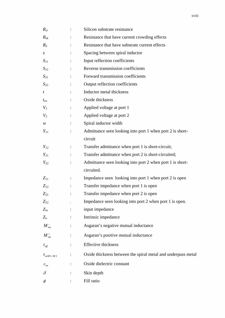
Rsi : Silicon substrate resistance
Rsk : Resistance that have current crowding effects
Rδ : Resistance that have substrate current effects
s : Spacing between spiral inductor
S11 : Input reflection coefficients
S12 : Reverse transmission coefficients
S21 : Forward transmission coefficients
S22 : Output reflection coefficients
t : Inductor metal thickness
tox : Oxide thickness
V1 : Applied voltage at port 1
V2 : Applied voltage at port 2
w : Spiral inductor width
Y11 : Admittance seen looking into port 1 when port 2 is short-
circuit
Y12 : Transfer admittance when port 1 is short-circuit;
Y21 : Transfer admittance when port 2 is short-circuited;
Y22 : Admittance seen looking into port 2 when port 1 is short-
circuited.
Z11 : Impedance seen looking into port 1 when port 2 is open
Z12 : Transfer impedance when port 1 is open
Z21 : Transfer impedance when port 2 is open
Z22 : Impedance seen looking into port 2 when port 1 is open.
Zin : input impedance
Zo : Intrinsic impedance −totM : Asgaran’s negative mutual inductance
+totM : Asgaran’s positive mutual inductance
efft : Effective thickness
21 MoxMt − : Oxide thickness between the spiral metal and underpass metal
oxε : Oxide dielectric constant
δ : Skin depth
φ : Fill ratio

xix
α1 : monomial data fit coefficient for outer diameter
α2 : monomial data fit coefficient for width
α3 : monomial data fit coefficient for average diameter
α4 : monomial data fit coefficient for number of turns
α5 : monomial data fit coefficient for spacing
β : beta, monomial data fit coefficient
γ : propagation constant
µ : Permeability
µo : Free space permeability
π : 22/7
ρ : Resistivity
σAl : Aluminum conductivity
σAu : Gold conductivity
σCu : Copper conductivity
Φ : Magnetic flux
ω : radian frequency, rad/s
Ω : Unit of resistivity, ohm
xx
LIST OF APPENDIXES
APPENDIX A: Two port networks ......................................................................... 123
APPENDIX B: Integrated Spiral Inductor Layout View......................................... 126
APPENDIX C: Integrated Spiral Inductor Synthesis Using EXCEL ...................... 128
APPENDIX D:Integrated Spiral Inductor Macro Model Extraction and Optimization
Using EXCEL................................................................................................. 131
APPENDIX E: PSPICE Format of Global Integrated Inductor Model ................... 134
APPENDIX F: List of Publications ......................................................................... 135

Chapter I
INTRODUCTION
The demand of consumer products such as the mobile phone, personal digital
assistant or mobile computer with wireless feature has seen a tremendous growth
recently. This has created a stronger demand for low cost, low power consumption,
high volume implementation of radio frequency (RF) functions in consumer
products.
Most of the current radio frequency integrated circuits (RFIC) are
implemented in the matured Gallium Arsenide (GaAs) technology. However, the
complementary metal-oxide-silicon (CMOS) process, which is currently in high
volume production for digital signal processors, is also emerging as one of the
options for RFICs [Larson, 1998]. The latest research development in the CMOS
technology has seen an increasing effort to migrate the RF applications onto the
silicon (Si) process. Following this trend, higher level of integration of RF, analog
and digital circuits using the conventional or innovative methods in CMOS process
are expected to happen in the near future [Burghartz, 1997].
2
Previously, inductors were not considered as standard components, such as
transistors, resistors or capacitors where models are included in the standard
technology library. However, the demands for inductors models are increasing, as RF
circuits on Si with acceptable performance are now feasible [Chan, et al., 2001]
[Wang, et al. 2002][Steyaert, et al. 2000]. Inductor models that are able to predict the
behavior of inductor over a broad range of frequency are important for circuit
simulation and layout optimization. Thus has arisen the need to develop a generic
procedure that is able to produce good inductor models for RFIC applications.
1.1. Research Background
As the CMOS technology continue to scale down to its next technology node,
the performance of the transistor continue to improve, in term of cut-off frequency
(ft) and maximum frequency (fmax). For example, ft for 0.18µm is reaching 50GHz,
which allows for RF applications operating below 10GHz. Nevertheless, there are
still some performance issues need to be solved, especially when the bottle neck
passive element, the inductor, is included in CMOS process. In the next two sub-
sections, the inductor’s application, the issues due to the physical structure of the
inductor in CMOS process and the motivation in this research will be discussed.
a.) Inductor’s Application In RF Design
The inductor is an indispensable part of many RF circuit block. One of the
applications of inductors is found in impedance matching. In RF systems,
impedance matching is critical to ensure maximum power transfer from one circuit
block to another circuit block when two circuit blocks are cascaded. Maximum
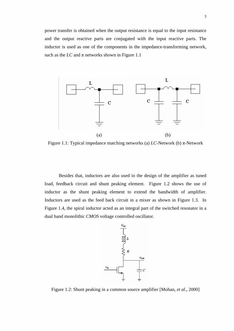
3
power transfer is obtained when the output resistance is equal to the input resistance
and the output reactive parts are conjugated with the input reactive parts. The
inductor is used as one of the components in the impedance-transforming network,
such as the LC and π networks shown in Figure 1.1
(a) (b)
Figure 1.1: Typical impedance matching networks (a) LC-Network (b) π-Network
Besides that, inductors are also used in the design of the amplifier as tuned
load, feedback circuit and shunt peaking element. Figure 1.2 shows the use of
inductor as the shunt peaking element to extend the bandwidth of amplifier.
Inductors are used as the feed back circuit in a mixer as shown in Figure 1.3. In
Figure 1.4, the spiral inductor acted as an integral part of the switched resonator in a
dual band monolithic CMOS voltage controlled oscillator.
Figure 1.2: Shunt peaking in a common source amplifier [Mohan, et al., 2000]

4
Figure 1.3: Schematic of mixer [Wang, et al., 2002]
Figure 1.4: Schematic of a dual-band VCO [Yim, et al. ,2001]
The quality (Q) factor of the CMOS inductor is generally very low, around 8
to 15, which is not suitable for filter that requires high Q passive elements.
Nevertheless, if the inductor is combined with transistor, the Q of the inductor can be
drastically improved. In this case, the transistor acted as the negative resistance
generator, which will reduce the real portion of the impedance of the inductor when
connected to the transistor and thus increased the Q. This is then enabled the on-chip

5
inductors to be used to implement the RF filters, for example the band pass filter as
shown in figure 1.5 [Sooranpanth and Wong, 2001].
Figure 1.5 : 2140±30 MHz, 3rd order Chebyshev filter [Sooranpanth and Wong,
2001].
b.) Inductor On Silicon
Researchers are investigating the possibility in migrating the expensive GaAs
process to the cheaper Si IC technology for RF applications. Inductor is one of the
key devices in such an investigation. Unlike other devices, such as the capacitors
and the transistors, the integrated inductor is relatively “new” in RFIC. Previously,
the inductor is either realized off-chip or bond-wire. This has made the whole circuit
to become bulky, difficult to control (for the case of bond-wire), less integrated and
thus more expensive. The integrated inductors in CMOS usually have lower Q

6
factor, in the order 5 to 15, compared to capacitors, which are usually in the order of
few hundreds in 1 to 2 GHz range.
A typical IC process in 0.18µm CMOS technology has six layers of
Aluminum (Al) interconnects, as shown in Figure 1.6 shows the cross-sectional view
of six layer metal in CMOS process. At the first glance, some may think that the
inductor can be fabricated using any of the six layers. However, in reality, it is
usually only the top layer or only a few layers at the top are used. Inductor on Si
substrate suffers a few intrinsic Q limiting factors.
Figure 1.6: Cross-section of metal 6 layers aluminum metal in a typical IC process
Inductors are formed on the top metal to reduce the parasitic capacitance of
the inductor. For example, to fabricate the circular spiral shown in Figure 1.7, metal
6 is used to draw the circular spiral inductor and metal 5 is used to draw the
underpass metal.

7
Figure 1.7: Circular spiral inductor
Most of the IC manufacturers, which are the foundries, also offer thicker top
metal option for the construction of inductor, in 0.18 µm CMOS analog process, top
metal (Aluminum) thickness is 2 µm, resulting the sheet resistance, around 15 mΩ/
(mili-Siemen per square) [Keating, et al., 2002]. Other metal layer, such as metal 5
and below, the metal thickness is more than 50% thinner. Higher resistances are
expected for these metals and it is therefore going to cause the increase of the metal
loss and subsequently decrease the Q-factor.
At higher frequencies, current crowding due to two effects, namely the skin
effects and proximity effects. These effects will cause an uneven current distribution
in the metal. In the skin effects, the center portion of the conductor will be enveloped
by a greater magnetic flux than those on the outside. Consequently the self induced
back electromagnetic flux will be greater towards the center of the conductor, thus
causing the current density to be less at the center than the conductor surface. This
extra concentration at the surface results in an increase in the effective resistance of
the conductor as the frequency increases.
8
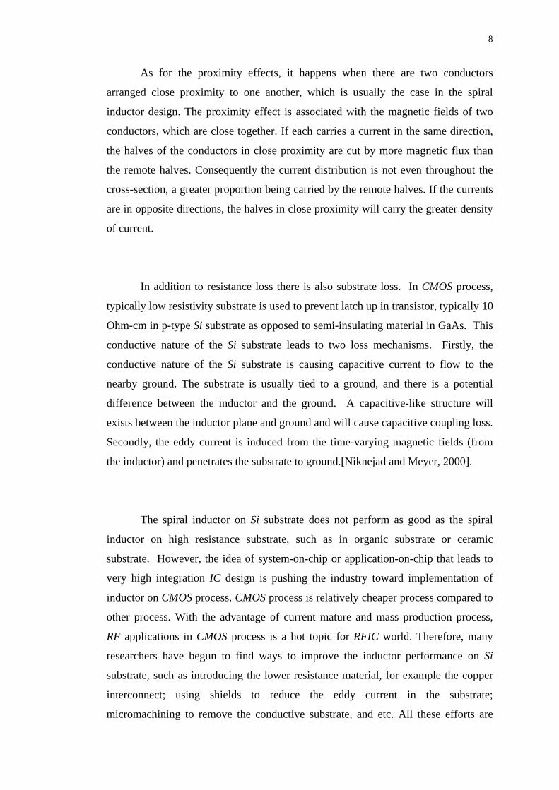
As for the proximity effects, it happens when there are two conductors
arranged close proximity to one another, which is usually the case in the spiral
inductor design. The proximity effect is associated with the magnetic fields of two
conductors, which are close together. If each carries a current in the same direction,
the halves of the conductors in close proximity are cut by more magnetic flux than
the remote halves. Consequently the current distribution is not even throughout the
cross-section, a greater proportion being carried by the remote halves. If the currents
are in opposite directions, the halves in close proximity will carry the greater density
of current.
In addition to resistance loss there is also substrate loss. In CMOS process,
typically low resistivity substrate is used to prevent latch up in transistor, typically 10
Ohm-cm in p-type Si substrate as opposed to semi-insulating material in GaAs. This
conductive nature of the Si substrate leads to two loss mechanisms. Firstly, the
conductive nature of the Si substrate is causing capacitive current to flow to the
nearby ground. The substrate is usually tied to a ground, and there is a potential
difference between the inductor and the ground. A capacitive-like structure will
exists between the inductor plane and ground and will cause capacitive coupling loss.
Secondly, the eddy current is induced from the time-varying magnetic fields (from
the inductor) and penetrates the substrate to ground.[Niknejad and Meyer, 2000].
The spiral inductor on Si substrate does not perform as good as the spiral
inductor on high resistance substrate, such as in organic substrate or ceramic
substrate. However, the idea of system-on-chip or application-on-chip that leads to
very high integration IC design is pushing the industry toward implementation of
inductor on CMOS process. CMOS process is relatively cheaper process compared to
other process. With the advantage of current mature and mass production process,
RF applications in CMOS process is a hot topic for RFIC world. Therefore, many
researchers have begun to find ways to improve the inductor performance on Si
substrate, such as introducing the lower resistance material, for example the copper
interconnect; using shields to reduce the eddy current in the substrate;
micromachining to remove the conductive substrate, and etc. All these efforts are
9
trying to integrate the RF section into the existing digital section on chip. Looking at
the current research activities trend, the production of a full RF system build on Si
substrate is coming nearer at our doorstep.
1.2 Objectives and scopes of research
The main objective of this research is to meet the needs of the coming
implementation of integrated inductor in CMOS process. It is to provide know-how
knowledge in the synthesis and modeling of integrated inductor. The inductor model
will be developed and readied before the implementation of inductor application on
CMOS process. Hence, the scopes of this research are to study and develop a generic
procedure of both inductor synthesis and inductor modeling. The products of this
research will include a simple and easy implementation of inductor synthesis and an
extraction, optimization procedure for integrated inductor.
1.3 Thesis Organization
Chapter I presents the introductions of this research work, which includes the
research background, research objectives and scope of research. Chapter II presents
the discussions of previous works from literatures. The rest of the chapters cover
three main parts of this thesis, the first part is devoted to the RF integrated planar
spiral inductor synthesis. The focus of chapter III is on the physical model and the
synthesis of planar spiral inductor. The details of the physical model of the inductor
are reviewed. Comparisons of a few inductance expressions for square inductor are
done. The most accurate closed form inductance expression is identified and
described in this work. The optimum inductor design with the help of the contour
10
plot of Q is described. An example on synthesizing an inductor for 3nH is shown.
The second part of the thesis is on the modeling and optimization of integrated spiral
inductor, which is covered in Chapter IV. In this chapter, it is presented a new
proposed model extraction procedure. The improvements of the new proposed
method are highlighted. A generic model optimization methodology is included in
this chapter. One of the wide-band modeling methods is also discussed. The third
part describes a new global integrated inductor model. Chapter V presents a break
through in inductor modeling. The physical modeling and extraction modeling are
combined and produced the global integrated inductor model (GIIM). Chapter VI
concludes the thesis. Recommendations and suggestions for future work are
presented.


![Download [2.45 MB]](https://img.dokumen.tips/doc/110x75/587f44871a28ab8a5f8c3deb/download-245-mb.jpg)