Embed Size (px)
Citation preview

Synthesis and ethanol sensing properties of indium-doped tin oxide nanowiresX. Y. Xue, Y. J. Chen, Y. G. Liu, S. L. Shi, Y. G. Wang, and T. H. Wang Citation: Applied Physics Letters 88, 201907 (2006); doi: 10.1063/1.2203941 View online: http://dx.doi.org/10.1063/1.2203941 View Table of Contents: http://scitation.aip.org/content/aip/journal/apl/88/20?ver=pdfcov Published by the AIP Publishing Articles you may be interested in Plasma-produced phase-pure cuprous oxide nanowires for methane gas sensing J. Appl. Phys. 115, 124310 (2014); 10.1063/1.4869435 Vertically aligned tin-doped indium oxide nanowire arrays: Epitaxial growth and electron field emission properties Appl. Phys. Lett. 89, 123102 (2006); 10.1063/1.2345278 Growth and luminescence properties of micro- and nanotubes in sintered tin oxide J. Appl. Phys. 97, 044316 (2005); 10.1063/1.1851602 Tailored nanoparticle films from monosized tin oxide nanocrystals: Particle synthesis, film formation, and size-dependent gas-sensing properties J. Appl. Phys. 93, 551 (2003); 10.1063/1.1525855 Physical properties of osmium doped tin oxide thin films J. Appl. Phys. 83, 2369 (1998); 10.1063/1.366982
This article is copyrighted as indicated in the article. Reuse of AIP content is subject to the terms at: http://scitation.aip.org/termsconditions. Downloaded to IP:
137.30.242.61 On: Wed, 10 Dec 2014 12:32:09

Synthesis and ethanol sensing properties of indium-dopedtin oxide nanowires
X. Y. Xue, Y. J. Chen, Y. G. Liu, S. L. Shi, Y. G. Wang, and T. H. Wanga�
Micro-NanoTechnologies Research Center, Hunan University, Changsha 410082, Institute of Physics,Chinese Academy of Sciences, Beijing 100080, and School of Science, Harbin Engineering University,Harbin 150001, China
�Received 4 January 2006; accepted 17 April 2006; published online 16 May 2006�
Indium-doped tin oxide �ITO� nanowires are synthesized in mass production via thermalevaporation of In2O3, SnO, and graphite mixture powders. The transverse sizes of these nanowiresrange from 70 to 150 nm, and the lengths are up to several tens of micrometers. The three elementsIn, Sn, and O uniformly distribute over the whole nanowire, respectively. The atomic concentrationof In is about 5%. The gas sensors realized from these ITO nanowires are very sensitive to ethanolgas, and the sensitivity is about 40 against 200 ppm ethanol at the work temperature of 400 °C.Both the response and recovery time are shorter than 2 s. These results suggest that ITO nanowiresare good candidates for fabricating gas sensors. © 2006 American Institute of Physics.�DOI: 10.1063/1.2203941�
One-dimension �1D� nanostructures of semiconductingmetal oxide have attracted great attention for their distinctiveoptical, chemical, electrical, and gas sensing properties.1–6
Especially, SnO2 and In2O3 1D nanostructures have attractedmore attention because of their potential applications inelectronics,3 gas sensors,4,5 and optoelectronics.6 Nowadays,more effort has been taken to investigate composite In–Sn–O1D nanostructures due to their promising applications innanodevices.7,8 Recently, ITO thin film materials are widelyused in fabricating gas sensors and their sensitivity againstethanol gas is very high.9,10 Usually, 1D nanostructures aremore sensitive than bulk materials due to their high surface-to-volume ratio.11,12 However, the gas sensors fabricatedfrom ITO nanowires still have not been reported so far.
In this letter, we synthesize ITO nanowires in mass pro-duction via thermal evaporation of In2O3, SnO, and graphitemixture powders. And we have already used this simplemethod to synthesize composite Zn–Sn–O nanowires.12
Similar synthesis strategy could be used to produce variousmetal-doped tin oxide 1D nanostructures. Various experi-mental analyses on these ITO nanowires provide the aspectand size, characterize the structure, and identify the compo-nents. The photoluminescence �PL� spectra show a strongand broad peak around 617 nm in air at room temperature,and this visible emission probably arises from the surfacedefect states. The gas sensors fabricated from these ITOnanowires exhibit high response to ethanol gas. The sensitiv-ity is up to about 40 against 200 ppm ethanol, and both theresponse and recovery time are shorter than 2 s. Such etha-nol sensing is attributed to the adsorption and desorption ofthe oxygen on the surface. Mass production, high sensitivity,and fast response suggest that ITO nanowires can be used inindustrial production of gas sensors.
ITO nanowires were synthesized by thermal evaporation,similar to that reported for the synthesis of ZnSnO3 nano-wires in Ref. 12. A thin �about 4 nm� Au film was sputteredon the n-type Si �001� substrates, and high pure �99.99%�
In2O3, SnO, and graphite powders with the weight ratio of4:1:4 were mixed thoroughly. The mixture was then loadedin an alumina boat, and the substrate was positioned on theboat. The alumina boat was placed at the center of a quartztube which was inserted in a horizontal tube furnace. Thefurnace was then heated to 930 °C and kept at this tempera-ture for 2 h. At this step, a mix gas of pure argon and smallamount of oxygen was introduced into the quartz tube at aflow rate of 20 SCCM �SCCM denotes cubic centimeter perminute at STP�, and the pressure in the quartz tube wasmaintained at 300 Pa. After the furnace cooled down to roomtemperature, the yellowish resulting products on the Si sub-strate were collected. The morphology, crystal structure, andcomponents of the products were analyzed by scanning elec-tron microscope �SEM; JEOL-JSM-6700F�, x-ray powderdiffraction �XRD; D/max 2550 V, Cu K� radiation�, andtransmission electron microscope �TEM; Tecnai F20� with anenergy dispersive x-ray spectrometer �EDS�, respectively. PLmeasurements were taken, and the ethanol sensing propertiesof the nanowires were carefully investigated.
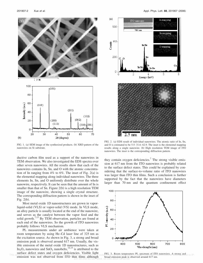
Figure 1�a� is a typical SEM image of the synthesizedproducts on the Si substrate, showing the general morphol-ogy of the products. They are highly dominated by the nano-wires with transverse size ranging from 70 to 150 nm andlengths of several tens of micrometers. In order to determinethe crystal structure of these nanowires, XRD experimentswere conducted. A XRD profile pattern is shown in Fig. 1�b�.There are three major diffraction peaks, which are indexed tothe �110�, �101�, and �211� crystal lattice planes of a rutilestructure of bulk SnO2. And all the other peaks also coincideto the peaks of such rutile structure of SnO2 given by thestandard data file �JCPDS file No. 41-1445�. It should benoted that the peaks of In2O3 have not been observed.
In order to check whether In is doped in these yellowishnanowires, the EDS analysis attached to TEM was per-formed to examine the components of individual nanowires.Figure 2�a� is an EDS spectrum taken from a single nano-wire, showing that the nanowire contains In, Sn, and O.Their atomic ratio is about 5.5: 31.6: 62.9. The presence ofCu and C peaks comes from the copper grids and the con-
a�Author to whom correspondence should be addressed; electronic mail:[email protected]
APPLIED PHYSICS LETTERS 88, 201907 �2006�
0003-6951/2006/88�20�/201907/3/$23.00 © 2006 American Institute of Physics88, 201907-1 This article is copyrighted as indicated in the article. Reuse of AIP content is subject to the terms at: http://scitation.aip.org/termsconditions. Downloaded to IP:
137.30.242.61 On: Wed, 10 Dec 2014 12:32:09
ductive carbon film used as a support of the nanowires inTEM observation. We also investigated the EDS spectra overother seven nanowires. All the results show that each of thenanowires contains In, Sn, and O with the atomic concentra-tion of In ranging from 4% to 6%. The inset of Fig. 2�a� isthe elemental mapping along individual nanowires. The threeelements In, Sn, and O uniformly distribute over the wholenanowire, respectively. It can be seen that the amount of In issmaller than that of Sn. Figure 2�b� is a high resolution TEMimage of the nanowire, showing a single crystal structure.The corresponding diffraction pattern is shown in the inset ofFig. 2�b�.
Most metal oxide 1D nanostructures are grown in vapor-liquid-solid �VLS� or vapor-solid �VS� mode. In VLS mode,an alloy particle is usually located at the end of the nanowire,and serves as the catalyst between the vapor feed and thesolid growth.7,13 By TEM observation, particles are found ateach end of the nanowires. So the growth of ITO nanowiresprobably follows VLS mechanism.
PL measurements under air ambience were taken atroom temperature by using He–Cd laser line of 325 nm asthe excitation source. As shown in Fig. 3, a strong and broademission peak is observed around 617 nm. Usually, the vis-ible emission of the metal oxide 1D nanostructures, such asIn2O3 nanowires and SnO2 nanobelts,14,15 is attributed to thesurface defect states and oxygen deficiencies. Visible lightemission was not observed from ITO thin films although
they contain oxygen deficiencies.7 The strong visible emis-sion at 617 nm from the ITO nanowires is probably relatedto the surface defect states. This could be explained by con-sidering that the surface-to-volume ratio of ITO nanowireswas larger than ITO thin films. Such a conclusion is furthersupported by the fact that the nanowires have diameterslarger than 70 nm and the quantum confinement effect
FIG. 1. �a� SEM image of the synthesized products. �b� XRD pattern of thenanowires on Si substrate.
FIG. 2. �a� EDS result of individual nanowires. The atomic ratio of In, Sn,and O is estimated to be 5.5: 31.6: 62.9. The inset is the elemental mappingresults along a single nanowire. �b� High resolution TEM image of ITOnanowires. The inset is the corresponding diffraction pattern.
FIG. 3. Room temperature PL spectrum of ITO nanowires. A strong andbroad emission peak is observed around 617 nm.
201907-2 Xue et al. Appl. Phys. Lett. 88, 201907 �2006�
This article is copyrighted as indicated in the article. Reuse of AIP content is subject to the terms at: http://scitation.aip.org/termsconditions. Downloaded to IP:
137.30.242.61 On: Wed, 10 Dec 2014 12:32:09

should be neglected. The emission cannot be related to quan-tum confinement effect. So it is quite reasonable to assumethat the emission is related to the surface defect states.
These ITO nanowires were then used to fabricate gassensors. The nanowires were ultrasonically dispersed in eth-anol for 2 h, and dried at 80 °C for 1 h. The ITO nanowirepaste was then laid uniformly on the ceramic tubes of the gassensors. Two Pt electrodes were placed on the surface of theceramic tube, and a heating resistance coil was inserted intothe tube.12 The nanowire paste completely covered the twoPt electrodes. The sensors were dried at 100 °C for 1 h, anda 24 h aging process was performed. Then, the sensors wereconnected to the outside electronic circuits, which monitoredthe change of the sensor resistance. The resistance changedafter putting the sensor in the gas chamber, which was in-stalled with test gases. Usually, the sensitivity S is defined asRa /Rg, where Ra is the resistance in air ambience, and Rg isthe resistance in ethanol and air mixed gas.11,12
Figure 4 shows the response and recovery of ITO nano-wire gas sensors upon exposure 10, 30, 50, 200, 500, and1000 ppm ethanol. The heating voltage is 6 V, and the worktemperature is about 400 °C. The environment humidity isabout 20% RH �relative humidity at 20 °C�. The sensorshows high response to ethanol gas, and both the responseand recovery time are shorter than 2 s. At 200 ppm ethanolexposure, the sensitivity is up to about 40. It is relativelyhigher than that of ITO thin film materials.10 The high andfast response of ITO nanowire gas sensors supports theirpromising applications in the industry.
Usually, the high gas sensing performance of 1D nano-structures is attributed to adsorption and desorption of oxy-gen on the surface with the large surface-to-volumeratio.11,12,16 By only considering a single ITO nanowire, thesensing process is simply shown in the inset of Fig. 4. Andthis sensing mechanism is similar to that discussed in Refs.
11 and 12. When the sensors are in air ambience, some oxy-gen molecules will adsorb on the surface of ITO nanowires.The adsorbed oxygen molecules capture free electrons fromthe nanowires, and become oxygen ions�O−, O2−, or O2
−�. This leads to a partial depletion of thenanowires, reduces the conductive width of the nanowires,and decreases the conductance. When the sensors were put inthe experimental chamber containing a certain concentrationof ethanol gas, ethanol molecules will react with the oxygenions and the electrons were released back into the nanowires.This reaction has been discussed in Ref. 12. This processdecreases the depletion width and increases the conductance.Such adsorbed oxygen and large surface-to-volume ratio leadto the high response of ITO nanowire gas sensors. On theother hand, the nanowire network probably increases the rateof oxygen adsorption and reduces the recovery time.
In conclusion, ITO nanowires are synthesized in massproduction by thermal evaporation method. The gas sensorsfabricated from these ITO nanowires were very sensitive toethanol gas, and both the response and recovery processeswere very fast. Our results strongly suggested that ITO nano-wires could be used to realize gas sensors at the industrylevel.
This work was partly supported from the Chinese Min-istry of Education �Grant No. 705040�, the Special Funds forMajor State Basic Research Project �No. G2001CB3095�,and the National Natural Science Foundation of China �Nos.69925410, 60236010, and 60571044�.
1Z. W. Pan, Z. R. Dai, and Z. L. Wang, Science 291, 1947 �2001�.2J. J. Liu, M. H. Yu, and W. L. Zhou, Appl. Phys. Lett. 87, 172505 �2005�.3J. F. Conley, Jr., L. Stecker, and Y. Ono, Appl. Phys. Lett. 87, 223114�2005�.
4E. Comini, G. Faglia, G. Sberveglieri, Zhengwei Pan, and Zhonglin Wang,Appl. Phys. Lett. 81, 1869 �2002�.
5Y. J. Chen, X. Y. Xue, Y. G. Wang, and T. H. Wang, Appl. Phys. Lett. 87,233503 �2005�; Y. J. Chen, L. Nie, X. Y. Xue, Y. G. Wang, and T. H.Wang, ibid. 88, 083105 �2006�.
6S. Q. Li, Y. X. Liang, and T. H. Wang, Appl. Phys. Lett. 87, 143104�2005�.
7Q. Wan, S. T. Song, S. L. Feng, and T. H. Wang, Appl. Phys. Lett. 85,4759 �2004�.
8H. S. Jang, D. Kim, H. Lee, and S. Lee, Mater. Lett. 59, 1526 �2005�.9V. S. Vaishnav, P. D. Patel, and N. G. Patel, Thin Solid Films 487, 277�2005�.
10Z. Jiao, M. H. Wu, J. Z. Gu, and X. L. Sun, Sens. Actuators B 94, 216�2003�.
11Q. Wan, Q. H. Li, Y. J. Chen, T. H. Wang, X. L. He, J. P. Li, and C. L. Lin,Appl. Phys. Lett. 84, 3654 �2004�.
12X. Y. Xue, Y. J. Chen, Y. G. Wang, and T. H. Wang, Appl. Phys. Lett. 86,233101 �2005�; X. Y. Xue, Y. J. Chen, Q. H. Li, C. Wang, Y. G. Wang, andT. H. Wang, ibid. 88, 182102 �2006�.
13X. F. Duan and C. M. Liber, Adv. Mater. �Weinheim, Ger.� 12, 298�2000�.
14G. Faglia, C. Baratto, G. Sberveglieri, M. Zha, and A. Zappettini, Appl.Phys. Lett. 86, 011923 �2005�.
15Y. B. Li, Y. S. Bando, and D. Golberg, Adv. Mater. �Weinheim, Ger.� 15,581 �2003�.
16O. Kryliouk, H. J. Park, H. T. Wang, B. S. Kang, T. J. Anderson, F. Ren,and S. J. Pearton, J. Vac. Sci. Technol. B 23, 1891 �2005�.
FIG. 4. Response and recovery characteristics of the gas sensors fabricatedfrom ITO nanowires exposed to various concentrations of ethanol gas at400 °C. The inset is the schematic diagram of the sensing process. Thedepletion width on the surface is narrower in ethanol gas than that in air.
201907-3 Xue et al. Appl. Phys. Lett. 88, 201907 �2006�
This article is copyrighted as indicated in the article. Reuse of AIP content is subject to the terms at: http://scitation.aip.org/termsconditions. Downloaded to IP:
137.30.242.61 On: Wed, 10 Dec 2014 12:32:09


![GaN based UV‐LEDs with Ni/Au Nanomeshes as Transparent …static.tongtianta.site/paper_pdf/2f697500-c569-11e9-ba50...of indium-free TCE such as Al-doped zinc oxide (AZO)[9] or Ga-doped](https://img.dokumen.tips/doc/110x75/60fa722c4a138a60367eecbf/gan-based-uvaleds-with-niau-nanomeshes-as-transparent-of-indium-free-tce.jpg)


![3D-AFM Nano-structural Features and Magnetic Properties of Indium-Doped Vanadate ... · 2020. 9. 27. · thermodynamic stability of bismuth vanadate-based compositions [9]. Based](https://img.dokumen.tips/doc/110x75/6081c316e3d07c0e3b322aa6/3d-afm-nano-structural-features-and-magnetic-properties-of-indium-doped-vanadate.jpg)


