Embed Size (px)
Citation preview

SYNTHESIS AND CHARACTERIZATION OF PHENANTHRO-IMIDAZOLE
BASED CONJUGATED COPOLYMER FOR OPTOELECTRONIC
APPLICATIONS
A THESIS SUBMITTED TO THE GRADUATE SCHOOL OF NATURAL AND APPLIED SCIENCES
OF MIDDLE EAST TECHNICAL UNIVERSITY
BY
NIMA SOHRABNIA
IN PARTIAL FULFILLMENT OF THE REQUIREMENTS FOR
THE DEGREE OF MASTER OF SCIENCE IN
POLYMER SCIENCE AND TECHNOLOGY
AUGUST 2016


Approval of the thesis: SYNTHESIS AND CHARACTERIZATION OF
PHENANTHRO-IMIDAZOLE BASED CONJUGATED COPOLYMER FOR
OPTOELECTRONIC APPLICATIONS
Submitted by Nima Sohrabnia in partial fulfillment of the requirements for the degree of Master of Science in Polymer science and Technology Department, Middle East Technical University to,
Prof. Dr. Gülbin Dural Ünver Director, Graduate School of Natural and Applied Sciences _____________ Prof. Dr. Necati Özkan Head of Department, Polymer Science and Technology _____________ Assoc. Prof. Dr. Ali Çırpan Supervisor, Department of Chemistry _____________ Assoc.Prof. Dr. H. Emrah Ünalan Co-Supervisor, Dept. of Metallurgical and Materials Eng., METU_____________ Examining Committee Members: Prof. Dr. Levent Toppare Chemistry Dept., METU ______________ Assoc. Prof. Dr. Ali Çirpan Chemistry Dept, METU ______________ Assoc. Prof. Dr. İrem Erel Göktepe Chemistry Dept, METU ______________ Assoc. Prof. Dr. Yasemin Arslan Udum Advanced Technologies Dept.,Gazi University ______________ Asst. Prof. Dr. Görkem Günbaş Chemistry Dept, METU ______________
Date: 24.08.2016

iv
I hereby declare that all the information in this document has been obtained
and presented in accordance with academic rules and ethical conduct. I also
declare that, as required by these rules and conduct, I have fully cited and
referenced all material and results that are not original to this work.
Name, Last Name:
Signature:

v
ABSTRACT
SYNTHESIS AND CHARACTERIZATION OF
PHENANTHRO-IMIDAZOLE BASED CONJUGATED COPOLYMER FOR
OPTOELECTRONIC APPLICATIONS
Sohrabnia, Nima
M.S., Department Polymer Science and Technology
Supervisor: Assoc. Prof. Dr. Ali Çırpan
Co-Supervisor: Assoc.Prof. Dr. H. Emrah Ünalan
August 2016, 68 pages
Benzodithiophene and flourene represent tremendous promise as donor moieties in
donor-acceptor approach for optoelectronic applications. The strong intermolecular
π-π stacking, coplanar and rigid structure as well as symmetric configuration of these
moieties enhance charge mobility and reduce band gap when incorporate in back
bone of polymer within pull and push system. In order to decrease angle torsion and
adjusting the optoelectronic properties of polymers, chalcogenophenes utilize as
bridge between donor and acceptor. In this study, three different phenanthro
imidazole containing conjugated copolymers (P1,P2 and P3) were synthesized using
benzodithiophene and flourene via Suzuki and Stille condensation reactions. The
structural characterizations of polymers were performed by NMR and the molecular
weight of these polymers was measured via GPC. P1 utilized as active layer in single
layer organic light emitting diode with device structure of
ITO/PEDOT:PSS/P1/LiF:Al. The observed color was cyan with luminance of 5560

vi
cd/m2 at 13 volts. For photovoltaic application P2 and P3 were used as active layer
with device structure of ITO/PEDOT:PSS/Polymer:PC71BM/Ca:Al. The best of
OPVs devices showed 0.94% PCE for P2 and 0.91% for P3 under standard AM 1.5
(100 mW/cm2) condition.

vii
ÖZ
OPTOELEKTRONİK UYGULAMALAR İÇİN FENANTREN-İMİDAZOL
İÇEREN KONJÜGE KOPOLİMERLERİN SENTEZİ VE KARAKTERİZASYONU
Sohrabnia, Nima
Yüksek Lisans, Polimer Bilim Ve Teknolojisi
Tez Yöneticisi: Doç. Dr. Ali Çırpan
Ortak Tez Yöneticisi: Doç. Dr. H. Emrah Ünalan
Ağustos 2016, 68 sayfa
Benzoditiyofen ve fluoren sahip olukları donor gruplarından dolayı optoelektronik
uygulamalar için çok büyük umut vaad etmektedirler. Bu donor grupların sahip
olduğu güçlü moleküler arası π-π dizinimi, eşdüzleme sahip olmaları, kararlı yapıları
ve simetrik dizilişlerinden dolayı yük akışını arttırırlar. Ayrıca bu gruplar polimerin
ana zincirinde bulunduklarında band aralığını düşürme özelliğine sahiptir.
Polimerlerin açısal bükülmesini ve optoelektronik özelliklerini arrtırmak için beş
halkalı köprüler alıcı ve verici guruplar arasında köprü olarak kullanılırlar. Bu
çalışmada fenantren -imidazol içeren üç farklı konjuge kopolimer Suzuki ve Stille
kenetlenme reaksiyonları ile gerçekleştirildi. Elde edilen polimerlerin yapısal
karakterizasyonu Nükleer Manyetik Rezonans (NMR) ile yapıldı ve polimerlerin
moleküler ağırlıkları Jel Süzülmeli Kromotografi (GPC) kullanılarak belirilendi. P1
tek tabaka olarak, ITO/PEDOT: PSS/P1/LiF:Al OLED cihaz yapısında aktif tabaka
olarak kullanıldı. Cam göbeği rengi yayan cihazın luminans değeri ise 13 Volt da
5560 cd/m2 olarak ölçüldü. ITO/PEDOT: PSS/Polymer: PC71BM/Ca:Al cihaz

viii
yapısında P2 ve P3 aktif tabakada kullanıldılar. AM 1.5 (100 mW/cm2) şartları
altında yapılan ölçümlerde, en iyi organik güneş pili sonuçları P2 için % 0.94 PCE,
P3 için ise % 0.91 PCE şeklindedir.

ix
To my gracious mother and altruist brother

x
ACKNOWLEDGEMENTS
I would like to indicate my extreme gratitude to my thesis supervisor Assoc. Prof.
Ali Çırpan. I owe thanks to him for endless efforts, precious feedback, patience and
encouragements during my thesis study. Also, I will not forget insight and
constructive criticism of Prof. Dr. Levent Toppare throughout in this study. Besides,
I am so grateful of my co-supervisor Assoc. Prof. Dr. H. Emrah Ünalan for his
guidence.
I express many thanks to my friends in Çırpan Research Group. My special thanks go
to Şevki Can Cevher, Gönül Hızalan, Şerife Özdemir Hacıoglu and Fatma Demir
helping during this study. During this research also students Emre Ataoğlu, Ipek
Önk, Ece Aktaş, Duygu Keleş and Özge Karagacti provided a great encourage,
comments and support to make this thesis as good as possible.
I am also indebted my lifelong friends Payam and Poorya Parvizi, Arif Badem,
Muzafer Gencay Celik and Ali Gharibdoost for their endless support, especially
during my thesis preparation.
My genuine appreciation goes to my amazing family members, my merciful Mom,
my gentle dad (R.I.P.) and my generous brother who always got my back in ups and
downs of life.

xi
TABLE OF CONTENTS
ABSTRACT ................................................................................................................. v
ÖZ .............................................................................................................................. vii
ACKNOWLEDGEMENTS ......................................................................................... x
TABLE OF CONTENTS ............................................................................................ xi
LIST OF TABLES .................................................................................................... xiv
LIST OF FIGURES ................................................................................................... xv
LIST OF ABBREVIATIONS ................................................................................. xviii
CHAPTERS
1.INTRODUCTION .................................................................................................... 1
1.1 SEMICONDUCTORS .............................................................................................. 1
1.1.1 Application of Semiconductors ................................................................... 2
1.1.2 Photovoltaics ............................................................................................... 2
1.1.2.1 Inorganic Photovoltaics ........................................................................ 2
1.1.2.2 Organic Photovoltaics .......................................................................... 3
1.1.3 Light Emitting Diodes ................................................................................. 4
1.1.3.1 Inorganic Light Emitting Diodes ......................................................... 4
1.1.3.2 Organic Light Emitting Diodes: ........................................................... 4
1.1.4 Electrochromic devices ............................................................................... 5
1.2 CONJUGATED POLYMERS: ................................................................................... 7
1.2.1 Band Gap Engineering ................................................................................ 9
1.3 ORGANIC PHOTOVOLTAICS ............................................................................... 10
1.3.1 Toward High Performance OPVs: ............................................................ 14
1.3.1.1 Donor Acceptor Approach ................................................................. 15
1.3.1.2 Narrow Band Gap: ............................................................................. 16
1.3.1.3 Morphology Optimization: ................................................................ 16

xii
1.3.2 Characterization of OPVs .......................................................................... 17
1.3.2.1 Short Circuit Current Density ............................................................ 17
1.3.2.2 Open Circuit Voltage ......................................................................... 17
1.3.2.3 Equivalent Circuit .............................................................................. 19
1.3.2.4 Fill Factor and Power Conversion Efficiency .................................... 20
1.4 ORGANIC LIGHT EMITTING DIODE .................................................................... 21
1.4.1 White Organic Light Emitting Diodes: ..................................................... 23
1.4.2 Color Quality of Polymer Light-Emitting Devices ................................... 24
1.4.3 Characterization of Polymer Light-Emitting Devices ............................... 25
1.5 MOTIVATION OF STUDY .................................................................................... 25
2.EXPERIMENTAL .................................................................................................. 29
2.1 MATERIALS ....................................................................................................... 29
2.2 INSTRUMENTATION ............................................................................................ 29
2.2.1 Electrochemical Studies ............................................................................ 29
2.2.2 Spectroelectrochemical Studies ................................................................. 30
2.2.3 Kinetic Studies .......................................................................................... 30
2.2.4 Thermal Analysis ...................................................................................... 30
2.2.5 Gel Permeation Chromatography .............................................................. 31
2.3 SYNTHESIS OF 2,5-DIBROMOTHIOPHENE-3-CARBALDEHYDE ............................. 31
2.8 SYNTHESIS OF 2-(2,5-DIBROMOTHIOPHEN-3YL)-1-(4-HEXYLPHENYL)-1H-
PHENANTHRO[9,10-D]IMIDAZOLE............................................................................ 32
2.9 SYNTHESIS OF 2-(2,5-DIBROMOTHIOPHEN-3-YL)-1-(4-FLUOROPHENYL)-1H-
PHENANTHRO[9,10-D]IMIDAZOLE............................................................................ 33
2.10 SYNTHESIS OF TRIBUTYL(4-HEXYLTHIOPHEN-2-YL)STANNANE ....................... 34
2.11 SYNTHESIS OF 2-(4,4''-DIHEXYL-[2,2':5',2''-TERTHIOPHEN]-3'-YL)-1-(4-
FLUOROPHENYL)-1H-PHENANTHRO[9,10-D]IMIDAZOLE ......................................... 34
2.12 SYNTHESIS OF 2-(5,5''-DIBROMO-4,4''-DIHEXYL-[2,2':5',2''-TERTHIOPHEN]-3'-
YL)-1-(4-FLUOROPHENYL)-1H-PHENANTHRO[9,10-D]IMIDAZOLE ........................... 35
2.13 SYNTHESIS OF P1 ............................................................................................. 36
2.14 SYNTHESIS OF P2 ............................................................................................. 37

xiii
2.15 SYNTHESIS OF P3............................................................................................. 38
2.16 ORGANIC PHOTOVOLTAIC DEVICE FABRICATION ............................................ 39
2.17 OLED DEVICE FABRICATION .......................................................................... 40
3.Results and discussion ............................................................................................ 41
3.1 SYNTHESIS ........................................................................................................ 41
3.2 CYCLIC VOLTAMMETRY .................................................................................... 42
3.3 SPECTROELECTROCHEMICAL STUDIES .............................................................. 44
3.4 KINETIC STUDIES .............................................................................................. 45
3.5 OPTICAL PROPERTIES OF POLYMERS ................................................................. 47
3.6 THERMAL ANALYSIS OF POLYMERS .................................................................. 48
3.7 POLYMER LIGHT EMITTING DIODE APPLICATION OF P1 .................................... 49
3.8 ORGANIC PHOTOVOLTAIC APPLICATION ........................................................... 51
4.Conclusion .............................................................................................................. 55
REFERENCES ........................................................................................................... 57
APPENDIX A ............................................................................................................ 61
NMR RESULTS .................................................................................................... 61
APPENDIX B ............................................................................................................ 67
THERMAL ANALYSIS RESULTS ................................................................................ 67

xiv
LIST OF TABLES
Tables
Table 1. Electrochemical Characteristics of P3. ........................................................ 44
Table 2. Switching Times and Optical Contrast in Near IR and Visible region ....... 46
Table 3. Optical Properties of Polymer. .................................................................... 48
Table 4. Optimization Studies of P2 and P3 for OPVs. ........................................... 53

xv
LIST OF FIGURES
Figures
Figure 1. Schematic Presentation of intersoliton hopping. ......................................... 8
Figure 2. Band Gap Diagram. ..................................................................................... 9
Figure 3. a) Resonance Structure of Polymers. b) Factor Effecting Band gap ......... 10
Figure 4. Conjugated Polymer P3HT as the Donor and PCBM as the Acceptor. ..... 11
Figure 5. The Structure of the Polymer That Shows Highest PCE Performed
Polymer in Literature. ................................................................................................ 12
Figure 6. Working principle of an OPV. .................................................................. 12
Figure 7. Foster and Dexter Energy Transfer ............................................................ 13
Figure 8. a) Donor and Acceptor Approach b) Hybridization resulting from D-A
approach c) Donor or Acceptor Moieties reproduced from[23] ................................ 15
Figure 9. Solar Spectrum in 1.5 G Condition Reproduced From [33]. ..................... 16
Figure 10. Equivalent Circuit of Organic Semiconductors Reproduced From [39]
.................................................................................................................................... 19
Figure 11. The Fill Factor and an Ideal cell Fill Factor reproduced from [23] ......... 21
Figure 12. Working Principle of OLED .................................................................... 22
Figure 13. Single Layer OLED Device structure ...................................................... 22
Figure 14. Fluorescence and Phosphorescence radiative decay. ............................... 23
Figure 15. Corresponding Angle of Phenanthroimidazole derivative of thiophene
reproduced from [47] ................................................................................................. 26
Figure 16.Structure of the Polymers. ........................................................................ 28
Figure 17. Synthesis of 2,5-dibromothiophene-3-carbaldehyde ............................... 31
Figure 18. Synthesis of 2-(2,5-dibromothiophen-3-yl)-1-(4-hexylphenyl)-1H-
phenanthro[9,10-d]imidazole ..................................................................................... 32
Figure 19. Synthesis of 2-(2,5-dibromothiophen-3-yl)-1-(4-fluorophenyl)-1H-
phenanthro[9,10-d]imidazole ..................................................................................... 33
Figure 20. Synthesis of tributyl(4-hexylthiophen-2-yl)stannane .............................. 34
Figure 21. Synthesis of 2-(4,4''-dihexyl-[2,2':5',2''-terthiophen]-3'-yl)-1-(4-
fluorophenyl)-1H-phenanthro[9,10-d]imidazole ....................................................... 34
xvi
Figure 22. Synthesis of 2-(5,5''-dibromo-4,4''-dihexyl-[2,2':5',2''-terthiophen]-3'-yl)-
1-(4-fluorophenyl)-1H-phenanthro[9,10-d]imidazole ................................................ 35
Figure 23. Synthesis of P1 ......................................................................................... 36
Figure 24. Synthesis of P2. ........................................................................................ 37
Figure 25. Synthesis of P3. ........................................................................................ 38
Figure 26. Cyclic Voltammetry of P1, P2 and P3 ..................................................... 43
Figure 27. Spectroelectrochmical Spectra of P3 and color at -2, 0, 1 and 1.1 V. ..... 45
Figure 28. Percent Transmittance Change of P3. ...................................................... 46
Figure 29. Uv-Visible Absorption Spectra of the Polymers (P1, P2 and P3) in
chloroform Solution and thin film. ............................................................................. 48
Figure 30. Photoluminescence of P1 in chloroform solution and thin film. ............. 49
Figure 31. P1. JLV Characteristics of P1 with Maximum Luminescence at 13 V and
1267 mA/cm2. ............................................................................................................. 50
Figure 32. The Electroluminescence of P1 at 12 V and maximum emission of 476
nm. .............................................................................................................................. 50
Figure 33. Color Coordinates of Emitted Light by P1. ............................................. 51
Figure 34. J-V characteristics of P2 and P3 .............................................................. 52
Figure 35. 1H NMR of 2,5-dibromothiophene-3-carbaldehyde ................................ 61
Figure 36. 1H NMR of 2-(2,5-dibromothiophen-3-yl)-1-(4-hexylphenyl)-1H-
phenanthro[9,10-d]imidazole ..................................................................................... 61
Figure 37. 13C NMR of of 2-(2,5-dibromothiophen-3-yl)-1-(4-hexylphenyl)-1H-
phenanthro[9,10-d]imidazole ..................................................................................... 62
Figure 38. 1H NMR of 2-(2,5-dibromothiophen-3-yl)-1-(4-fluorophenyl)-1H-
phenanthro[9,10-d]imidazole ..................................................................................... 62
Figure 39. 13C NMR of of 2-(2,5-dibromothiophen-3-yl)-1-(4-fluorophenyl)-1H-
phenanthro[9,10-d]imidazole ..................................................................................... 63
Figure 40. 1H NMR of 2-(4,4''-dihexyl-[2,2':5',2''-terthiophen]-3'-yl)-1-(4-
fluorophenyl)-1H-phenanthro[9,10-d]imidazole ........................................................ 63
Figure 41. 1H NMR of 2-(5,5''-dibromo-4,4''-dihexyl-[2,2':5',2''-terthiophen]-3'-yl)-
1-(4-fluorophenyl)-1H-phenanthro[9,10-d]imidazole ................................................ 64

xvii
Figure 42. 13C NMR of 2-(5,5''-dibromo-4,4''-dihexyl-[2,2':5',2''-terthiophen]-3'-yl)-
1-(4-fluorophenyl)-1H-phenanthro[9,10-d]imidazole. .............................................. 64
Figure 43. 1H NMR of P1. ........................................................................................ 65
Figure 44. 1H NMR of P2. ........................................................................................ 65
Figure 45. 1H NMR of P3. ........................................................................................ 66
Figure 46. DSC Thermogram of P1. ......................................................................... 67
Figure 47. DSC Themogram of P2. .......................................................................... 67
Figure 48. TGA Curve of P1. .................................................................................... 68
Figure 49. TGA Curve of P2. .................................................................................... 68

xviii
LIST OF ABBREVIATIONS
CE Coloration Efficiency
OD Optical Density
BLA Bond Length Alternation
PEDOT Poly (3, 4-ethylenedioxythiophene)
PV Photovoltaic
OPV Organic Photovoltaic
LED Light Emitting Diode
OLED Organic Light Emitting Diode
ITO Indium Tin Oxide
PCE Power conversion Efficiency
FRET Förster Resonant Energy Transfer
LUMO Lowest Occupied Molecular Orbital
HOMO Highest Occupied Molecular Orbital
Eg Band Gap
QE Quantum Efficiency
LE Iuminous Efficiency
Jsc Short Circuit Current Density
EQE External Quantum Efficiency
FF Fill Factor
DSC Differential Scanning Calorimeter
TGA Thermo Gravimetric Analysis
RGB Red, Green and Blue
LI Luminous Intensity
HTL Hole Transport Layer
JLV Current Density-Luminesce-Voltage
BDT Benzodithiophene
ECD Electrochromic device
1
CHAPTER 1
INTRODUCTION
1.1 Semiconductors
The useful way to describe conduction in materials is band gap theory. In this theory,
materials can be divided into three major class on basis of conduction. These are the
conductors (such as metals), insulator (such as saturated plastics) and
semiconductors. In conductors, the conduction band and valance band are overlap,
hence, electron can move freely in these materials. On the other hand, in insulators
the electron could not move in martials because large band gap (larger than 5 eV).
Semiconductors have band gap about 0.5-4.5 eV. Because of relatively smaller bad
gap, electrons can move to conduction band in certain condition. For example, under
illumination of light electrons exited and can move. Semiconducting materials can be
divided into two main group. The pioneer class of semiconductors are based on
inorganic materials whereas the new generation one is organic semiconductors. One
of the difference of these materials is the charge transfer mechanism. In inorganic
materials the drift and diffusion of the charge is main reason for charge transport.
However, in organic materials the hoping of electron to the empty state is the main
reason for charge transport. Another difference is their dielectric constant. Organic
materials have smaller dielectric constant result in formation of exitons with
relatively high columbic interaction compare to inorganic materials. This means the
charge separation in organic materials is more vital. To overcome this problem donor
acceptor molecule is utilized in organic materials.

2
1.1.1 Application of Semiconductors
The key concept in optoelectronic devices is the interchangeable transformation
between light and electricity which depends on interaction of electrons and light
within semiconductors. The band gap of semiconducting material is crucial for
desired application. By tuning the band gap of semiconductors, their properties can
be tailored from insulator to conductive materials. Electrochromic devices (ECDs),
Light Emitting Diodes (LEDs), Field Effect Transistors (FETs) and Photovoltaics
(PVs) are well-known examples of optoelectronic devices. The semiconductors
generally can be categorized as organic and inorganic. Inorganic ones have been
utilized in almost all electronic devices from early 20 centuries. However, the new
area in semiconductors emerged in the last 3 decades based on organic materials.
During these 30 years many efforts have been done to improve performance of these
devices. One of the promising approach is utilizing organic macromolecule, in other
words, conjugated polymers. The focus of this work is to synthesize novel
conjugated polymers for Organic Photovoltaics (OPV) and organic light emitting
diode OLED applications. In upcoming section of this chapter descriptions are given
to understand the difference between organics and inorganics in terms of
performance and engineering point of view. In sections (2,3 and 4) of this chapter a
great discussion on conjugated polymers; OPVs and OLEDs will be reviewed.
1.1.2 Photovoltaics
As the demand for renewable energy considering the limitations and disadvantages
of traditional fuels, photovoltaic (PV) cells have become a center of great attention.
These are semiconductors that output current directly from light. Records show
Alexandre Edmund Becquerel’s efforts and observations in obtaining current from
applying light to electrochemical cells in 1839 that actually pioneered this interesting
field.
1.1.2.1 Inorganic Photovoltaics
Although today, silicon based solar cells which constitute 90% of solar energy

3
produced all over the world have an efficiency of 25.6% using single crystal
materials and 21.3 % using the polycrystalline [1]. In fact, it was as low as 4% which
is a clear implication of advancement in the field [2]. Efficiency is dependent on
band gap (Eg) which is 1.1 eV in silicon where band gap for utmost quantum
efficiency (QE) for a single crystal is 1.3 eV, silicon has obtained great amount of
attention and significance. However, there are alternatives to this single crystal
silicon solar cells which reduce the manufacturing cost [1]. Nevertheless, advanced
multi-junction devices are produced which yields efficiency of up to 46.7 % based on
these materials. These devices show promising power conversion efficiency (PCE)
due to their high mobility of free carriers, high current density and high internal
quantum efficiency [3]. On the other hand, there are some problems with the devices,
most challenging of which are impossibility of integration onto flexible substrates in
crystal form and high production cost arising from the demand for high temperature
for integration of materials. As long as low-cost and high-efficiency are concerned,
researchers put their research focus on production thin layer, effective way to
purification of silicon and other alternative materials such as organic compounds.
1.1.2.2 Organic Photovoltaics
To attack the problem associated with the manufacturing of optoelectronic devices,
organic semiconductors including both polymers and small molecules are being used
widely. Having π-electron delocalization on their backbone, these molecules exhibit
certain conductivity features through intermolecular or intramolecular bonds. The
range of the energy gap in organic semiconductors is between 1.4-3.0 eV for
absorption in visible region and absorption to Near-IR region which enhance the
performance of organic photovoltaics [4]. Studies continue to increase the efficiency
and there has been developments from 1% to 11.7% nowadays [5]. Solution
processable conjugated polymers and thermally deposited small molecules are used
in manufacturing of organic photovoltaics. Since they show strong absorption
properties, the ease in purification and the possibility of being deposited onto flexible
substrates at low cost, polymers become center of consideration in applications
related to OPV and OLED [6].

4
1.1.3 Light Emitting Diodes
Considering the fact that nearly one-fifth of the global electricity consumption is due
to lightning and great portion of it is wasted as heat rather than light, calls for
determined investigation of light bulbs. Toward resolving this issue, substitution of
Compact Fluorescent Lights for incandescent was the first step however, so far the
best solution happen to be LED usage of which is expected to greatly expand in the
coming few years.
1.1.3.1 Inorganic Light Emitting Diodes
The first known LED dates back in early 20th century when H. J. Round found the
first one in 1907. However, it was commercialized after discovery of Holonyak
(Galium, Arsenic and Phosphorous); a red emitting LED. The white color was
achieved by stacking primary colors (red, green and blue) which have been used as
solid state lightning.
1.1.3.2 Organic Light Emitting Diodes:
Pope and coworkers reported the first electroluminescence from organic solids
composed of anthracene [7]. Nevertheless, it was Vincett’s effort of depositing
amorphous thin films of anthracene using vacuum sublimation that caused voltage
drop indicating the viability of vacuum sublimation method of small molecular
organic LED devices’ production. The first polymer LED in which a precursor
polymer was spin cased onto Indium Tin Oxide (ITO) coated glass was brought
about by Friend and constituents after achievements in fabrication of small molecular
OLEDs in 1990 [8]. Besides, in polymer based LED molecules covalently bonded to
each other and chains have van der waals interaction which increase the mechanical
properties of device. The solubility of polymers allows them to easily processing
specially for mass production via spin coating or inkjet printing. Other remarkable
advantages of OLEDs are full angle viewing, possibility of flexible display
depending on flexible coatings, high efficiency and many more to be explored.

5
1.1.4 Electrochromic devices
The reversible capability of material to alter its color depending on the potential
applied is called electrochromism and three types of them are known as inorganic
materials, organic small molecules and conjugated polymers [9]. Smart windows,
display panels and smart mirrors are some of the application areas of ECDs [10].
Inorganic material such as tungsten oxide (WO3) reported by Deb in 1969 is the
pioneer class of ECDs [11]. Since then a great amount of studies and researches have
conducted on these materials however, there are still problems associated with them
mainly; slow switching time and high cost of vacuum evaporation. Small organic
molecules are the alternatives which are utilized as chromic layer in device. Viologen
(1,1'-di-methyl-4,4'-bipyridilium) has been studied extensively for years and
commercialization has been done for rear view mirrors. Dication form of viologen is
transparent but radical cation molecules which have intense deep blue color can be
formed as a result of reductive electron transfer and by changing the alkyl groups on
nitrogen, color change in radical cation redox state can be achieved e.g. 4-
cyanophenyl instead of alky group transmits green [12].
Promising properties such as ease of processing, fast switching time and high
efficiency in coloration in conjugated polymer based electrochromic devices have
drawn great amount of attention [9]. These semiconductors change their color upon
applied potential. In other word, electrochemical redox of polymer result in changing
in absorbance of polymer. Upon oxidation of the polymers polaron which bears
positive charge forms on back bone of the polymer. These positively charged
moieties are concomitant by flux of counter ion from electrolyte. If this partially
doped state be further oxidized bipolaron can be formed that facilitate the reduction
of bandgap. Hence, during redox reaction band gap changes consequently the
observed color. In fact, EC martials can be divided into three classes based on their
optical states [13]. First type is distinguishable in the sense that it consists of one
colored state and a transparent one like poly (3, 4-ethylenedioxythiophene) known as
PEDOT which are used in applications related to smart windows [18,17]. The other
type has discrete colored states and does not have a bleaching state. They are used in

6
display panels since different redox colors are required. To mention an example of
this type thin film of polythiophene which could switch from blue to red would be an
appropriate one. The last type are polymers with more than two colored states and
get attention because of their versatility in EC applications like poly(3,4-
propylenedioxypyrrole). Fundamentally there are five parameters which make these
EC materials distinguishable. Firstly, the percent transmittance of an ECD at
different wavelengths on electromagnetic spectrum can be inferred from optical
contrast. More specifically the amount of light with a certain wavelength that is
reflected. Furthermore, optical stability at different potentials and optical bands on
spectrum can be investigated by considering the cycles showing transmittance
change. Next, deterioration of the active layer accounts for stability which affects the
efficiency of ECD. Irreversible redox reactions, heat dissipation and side products
from electron loss or gain processes upon oxidation and reduction of the materials
and contaminants are some of the most notable reasons that result in the
deterioration. Thirdly, the time it takes for a color transformation in materials to be
observed during oxidation and reduction processes which is known as switching time
or switching speed in the literature. Surface characteristics of thin films, conduction
of free charges in electrolyte and permeability of ions to the interface of the thin
films are factors that affect the switching time. Another distinguished parameter
associated with EC materials is related to how well an EC device functions i.e.
coloration efficiency (CE). In order to calculate the CE value, Qd charge transferred
per unit area, charge in optical density (OD) need to be known. The equations 1and 2
show these relations clearly [15].
( ) ( )
( ) Equation 1
OD( )Qd
log
Tb( )Tc( )
Qd Equation 2
where;
η (cm2 /C): The efficiency of the CE

7
Tb: Transmittance value at the bleached state
Tc: Transmittance value at the colored state
1.2 Conjugated Polymers:
Over past 50 years macromolecular science has had major impact in human life style.
From spandex in fashion to drug delivery systems polymers emerge not only
alternative materials but also promising ones. Recent advances in polymer science
and with new applications being researched, there is no reason to believe that the
revolution will stop any time soon. New area in polymer science was introduced in
1970s by discovery of Hideki Shirakawa, Yet Alan J. Heeger and Alan G.
MacDiarmid. They show that polyacetylene becomes conductive as a metal. In 1974,
Shirakawa and coworkers prepared polyacetylene utilizing Ziegler-Natta catalyst as a
silvery film. In spite of its metallic appearance it was not conductive. However, by
coworking of above mentioned scientists, oxidation of this polymer by halogen
vapours made it 7 orders of magnitude conductive than the former form of
polyacetylene [16]. In fact, treatment of polymer with halogens called ‘’doping’’ like
doping process in semiconductors. The presence of conjugated system on polymer
backbone is the key property in conductive polymers. In this system each bond has
one localized sigma (σ) bond which covalently hold atoms in molecules and double
bond delocalize π system. In fact, presence of a conjugated system makes polymers
conductive. The formation of charge carriers which are mainly electrons and holes is
vital for conductivity. The electrons can tunnel from neighboring position and fill the
hole result in formation of new hole. Hence, charge migration to long distance
happens by this mechanism.
Redox processes abstract electron or add electron to polymer. For example, in case of
polyacetylene iodine forms a triiodide ion. Removing of electron from valence band
of polymer create a hole which is localized and stabilized by counter ion, in this case
triiodide. This radical cation is known as polaron. By further oxidation of the
polymer bipolaron can be formed [17]. Besides solitons which are free radicals can
also be formed on backbone of the polymer by isomeration or bond length alternation

8
[18]. This neutral free radical can propagate in the polymer by transferring itself to a
neighboring polymer by hopping. This process called intersoliton hopping Figure 1
[19].
Figure 1. Schematic Presentation of intersoliton hopping.
After surprising discovery in 1970s, advance in in field have grown and
semiconducting properties of polymer draw attention in both industry and academia.
OPVs, OLEDs and OFETs are examples of such applications where conjugated
polymers were investigated in world wide. The mechanism, device architecture and
polymer characteristics are the main reasons that should be taken into account to
promote efficiency. The optically doping process are different than electrochemical
doping in these active compounds. The doping in these semiconductors is done by
formation of exitions. Before a detailed introduction of OPVs and PLEDs, band gap
which is an inherent property of semiconductors should be explained to clarify
conductivity of these materials. In fact, it is defined as the energy difference between
the highest occupied molecular orbital (HOMO) and the lowest unoccupied
molecular orbital (LUMO) energy levels or in another words the energy between
conduction band and valence bands of the materials [17]. Considering electrical
conductivity, materials are classified as conductors, insulators and semiconductors.
The valence band is partially filled in conductors that leaves empty space for
electrons to move along when exposed to an electric field. In insulators all valence
band is completely filled and conduction band is completely empty separated by a
large energy band gap. However, in semiconductors it is just the opposite of
insulators. Electrons can move to the conduction band from valence band. Figure 3
represent the band energy structures of different materials. Cyclic voltammetry and
photoemission yielding spectroscopy are used to determine the HOMO and LUMO

9
levels. The optical band gap can be determined from absorption onset of visible
absorption of polymers.
Figure 2. Band Gap Diagram.
1.2.1 Band Gap Engineering
By tuning the band gap (Eg) electronic properties of semiconducting polymers can be
tailored and it is often called Eg engineering. Understanding the effect of structural
factor will be helpful for designing optimum band gap. Conjugated polymers have
two resonance forms that are nondegenerate. These are aromatic and quinoid
structures. In the aromatic form π electrons are confined, whereas, in quinoid from of
the polymer π electrons are delocalized along the conjugated polymer chain which
simultaneously alter a single bond to a double bond and vice versa. These structures
are depicted in Figure 3a. The aromatic form of the polymer is more stable
energetically, however, the quinoid form has higher energy resulting in lowering the
band gap. Due to strong dependency of Eg on alternating in conjugated system, five
geometrical parameters will be discussed. The first one is bond length alternation
donated as BLA [20] . This can be defined as difference in bond lengths of multiple
bond and adjacent single bond. When quinoid structure is dominant in ground state
more double bond pops up between adjacent rings. Consequently, BLA decreases

10
and narrows the band gap. This factor can be quantified as EBLA. Another factor is
energy that require to transform aromatic structure to quinoid form. Hence, reducing
the aromatic stabilization resonance will narrow the band gap. The effect of this
parameter is quantified as Eres [21]. The third one is Substituents Effect, ESub, which
is the most utilized way in adjusting HOMO and LUMO. Introducing electron
donating group usually increases HOMO level and inserting electron withdrawing
group to polymer increases ionization potential and electron affinity. Last one is a
rotational disorder around the single bond Eθ [22]. This angle known as dihedral
angle which increases Eg as angle increases. By considering these factors Eg can be
expressed with the following formula. The effect of all above mentioned factors are
represented in Figure 3b [23].
re b Equation 3
Figure 3. a) Resonance Structure of Polymers. b) Factor Effecting Band gap
1.3 Organic Photovoltaics
The PV effect can be described as direct conversation of light to the current.
Utilizing organic based materials as the active part for PV devices is called OPVs. In

11
OPVs, small molecules or polymers can be used as the absorbing layer for the
generation of current. However, the potential of inkjet printing, recent advances in
synthesis of material beside engineering bandgap make conjugated polymers as the
promising materials for OPVs. In these devices electron rich polymers behave like
electron donor which is blended with electron acceptor materials such as phenyl-C61-
butyric acid methyl ester (PCBM). As a requirement these polymers should have a
conjugated π system. An example of extensively studied conjugated polymer; poly-3-
hexyl thiophene (P3HT), and electron accepting PCBM are presented in Figure 4.
Figure 4. Conjugated Polymer P3HT as the Donor and PCBM as the Acceptor.
In addition to design and developing materials, optimization of interface and
developing device structure will be helpful for commercialization. By placing these
factors in forefront the efficiencies of these devices have been boosted from 2.4% to
11.7% in the last decade [5]. For example, recently Yuan and et al demonstrated that
by utilizing novel additive and hydrocarbon solvent, morphology can be controlled
which leads to boosting of PCE from 6.7% to 11.7%. The chemical structure of this
polymer is depicted in Figure 5.

12
Figure 5. The Structure of the Polymer That Shows Highest PCE Performed Polymer in Literature.
The working principle of organic PVs is depicted in Figure 6. These steps are; 1.
Photo induced exiton formation, 2. Diffusion of exitons, 3. Charge separation and 4.
Charge transport. The properties of each layer will be discussed later in this section.
Figure 6. Working principle of an OPV.
1. Photo induced exciton formation: The photon absorption of conjugated polymer
and efficiency of OPVs are directly related to each other. As light is absorbed,
excition; an electron-hole pair forms. The formed excitions are called Frenkel
exitons. This form of excitions are localized on backbone of polymer hence extra
energy is required to overcome excition binding energy and generate free charge
carriers. Typically binding energy in organic material’s between from 0.3 and 1
eV[24].

13
2. Diffusion of excitons : Excitons have very short life times and during their lifespan
they cover a certain distance called as excition diffusion length. The diffusion of
excition can be describe with two mechanisms regarding their electronic states.
Singlet electronic state excitions diffuse via Förster Resonant Energy Transfer
(FRET) [25]. Dipole-dipole coupling interaction between donor and acceptor
describes this long range energy transfer (1-10 nm). Whereas, Dexter energy transfer
in which overlap of wave functions are required, triplet-triplet and singlet-singlet
energy transfer is allowed. These two mechanisms are depicted in Figure 7. This is
worth to say that former mechanism is valid to describe hopping mechanism in
polymer backbone whereas the intermolecular intersolition hopping mechanism
usually is described by hopping into empty states by randomLy distributed Density
of States [26]. The diffusion via these mechanisms to reach interface of donor-
acceptor is crucial for current generation. Hence, larger diffusion length enhances
current generation. However, as diffusion length increases another factor should be
considered which is exciton life time. In fact, via reducing in film thickness, both
these factors could be fulfilled. However, thinner film diminishes photon absorption
which is a drawback for current formation. Therefore, exciton lifetime, diffusion
length and film thickness should be taken into consideration to engineer high
performance OPVs.
Figure 7. Foster and Dexter Energy Transfer.

14
3. Charge separation: After diffusion of exciton to interface electron from LUMO of
the donor transferred to LUMO of the acceptor. The driving force for this transition
is energy difference of these two levels. After transferring process, the electron in
LUMO of the acceptor and hole in HOMO in donor interact by Columbic forces. In
CT states electronic structure of this state and morphology plays a crucial role.
4. Charge transport: One of the vital factor to increase efficiency of OPVs is
understanding of charge carrier transport and collection. The imbalance mobility of
charge carriers results in formation space charge (or depletion region) build-up which
dramatically decreases efficiency of the device. In bulk heterojunction devices
electron mobility usually is 2-3 orders of magnitude higher than hole mobility [27].
Because of difference in mobility of hole and electron, the possibility of
recombination increases [28]. In order to overcome this issue, thermal treatment have
been done. For example, Valentin et al show that the hole mobility of P3HT
increased 3 orders of magnitude by thermal annealing [27]. In fact, optimized
thermal annealing controls orientation and crystallization of polymer which improve
CT and collection at corresponding electrodes.
1.3.1 Toward High Performance OPVs:
In order to develop high performance OPV cells certain principles are needed to be
taken into consideration. Eg can be optimized by considering donor acceptor
approach.. Performance of the device can be further improved by bulk heterojunction
architecture where a greater interface area between polymer and acceptor is obtained.
Increasing the performance of the cell for the purpose of harvesting the solar energy
requires high absorption by polymer. Hence, it is expected that PCE can be higher
for a polymer having narrower Eg that absorbs in Near-Infrared region. The
performance of cell is affected by morphology of polymer and acceptor where to
have a high interface area is demanded. It is note-worthy also to mention that
efficiency is reduced by trapped domains where polymer and acceptor have not or
little interface with electrodes.
15
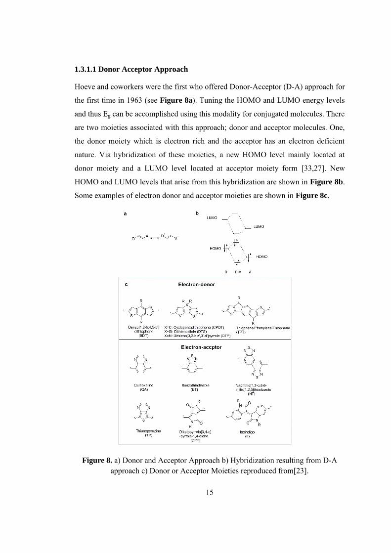
1.3.1.1 Donor Acceptor Approach
Hoeve and coworkers were the first who offered Donor-Acceptor (D-A) approach for
the first time in 1963 (see Figure 8a). Tuning the HOMO and LUMO energy levels
and thus Eg can be accomplished using this modality for conjugated molecules. There
are two moieties associated with this approach; donor and acceptor molecules. One,
the donor moiety which is electron rich and the acceptor has an electron deficient
nature. Via hybridization of these moieties, a new HOMO level mainly located at
donor moiety and a LUMO level located at acceptor moiety form [33,27]. New
HOMO and LUMO levels that arise from this hybridization are shown in Figure 8b.
Some examples of electron donor and acceptor moieties are shown in Figure 8c.
Figure 8. a) Donor and Acceptor Approach b) Hybridization resulting from D-A approach c) Donor or Acceptor Moieties reproduced from[23].

16
1.3.1.2 Narrow Band Gap:
Most efficient OPVs harvest much of the near-IR and visible regions of solar
radiation. As seen in Figure 10 these are the regions of maximum solar flux,
therefore there has been a great deal of attention focused on creating organic donor
and acceptor layers with lower band gaps (1.2 to1.6 eV), without sacrificing of
chemical stability [32].
Figure 9. Solar Spectrum in 1.5 G Condition Reproduced From [33].
1.3.1.3 Morphology Optimization:
Since the mixed thin film is not an equilibrium structure, phase segregation of this
mixture into an entangled heterojunction can be obtained by annealing the films at
optimal temperatures which will crystalize the film internally into the bulk structure.
However, a reduction in efficiency can be observed in some cases. This result shows
that the phase separation has resistive cul-de-sacs where the free charge has been
trapped before their collection at the electrodes [34].

17
1.3.2 Characterization of OPVs
In order to determine characteristics of PV cells, the J-V relation is investigated in
Air Mass (AM) 1.5 global condition. From this curve important parameters are
determined; Jsc and Voc . Hence, knowing the relation of current density and
potential, Fill Factor (FF) and PCE can be determined.
1.3.2.1 Short Circuit Current Density
The current which is generated when there is no external potential is called Jsc. It has
direct relation with external quantum efficiency (EQE) which is the ratio of the
number of incident photons to the number of generated charge carriers. This relation
is formulated in equation 4.
Equation 4
A is a parameter which is correlated with the light absorption efficiency. As the band
gap decreases the capability of light absorption increases, hence, EQE increases. ED
is the ability of exciton transfer of the interface of polymer and acceptor. The main
parameters affecting the diffusion performance is the morphology of the active
layer . Dissociation efficiency of excitons is known as da. The donor-acceptor
interface creates a charge transfer state. In this state the electron and hole are not
separated. Increasing the driving force for dissociation of the exciton at interface
increases this parameter. This force should be more than the exciton binding energy
which is about 0.3 eV. CT is the charge transfer to the corresponding electrode. The
migration of charges in the active layer is explained via hopping process influenced
by defects on the active layer and recombination of the excitons. cc is the efficiency
which explains the ability of electrodes for charge collection. Taking such
consideration on electrodes will increase charge flow and diminish formation of
space charge region on electrode and consequently current density[28,39].
1.3.2.2 Open Circuit Voltage
The potential measured between two electrodes when the current value is zero is

18
called Voc. This phenomenon can be described with tangible data with some
empirical approximations. Voc value of the device is described as the energy
difference between HOMO of the donor and LUMO of the acceptor molecules. By
the Scharber’s studies on this issue, a formula identifying the experimental Voc value
was published in 2006[36].
( ( ) ( )) Equation 5
The Voc loss of 0.3 eV is empirical, and the loss could be greater or smaller. It is
known that introduction of electron donating or withdrawing group on polymer
backbone result in tuning the relative energies of HOMO and LUMO [41,42].
Electron donating group increase the HOMO level and electron withdrawing one
diminish LUMO level. Therefore, tailoring the HOMO and LUMO levels Voc can be
tuned.
The recombination of carriers at donor acceptor interface develops dark saturation
current, resulting in the reduction of Voc in open circuit condition which can be
expressed by equation 6 [39].
(
) Equation 6
To inhabit the recombination, in other words, increase Voc, they are several
considerations to be taken to into account. The dissociation of excition strongly
depends on electric field at interface of donor-acceptor, hence, as the built in electric
field is larger, excition dissociation gets easier and a higher Voc is expected. Tada et
al showed by changing dipole moments of P3HT or PCBM can tune Voc from 0.3 to
0.9 V. In another approach Yuan and colleagues incorporate a ferroelectric polymer
layer in structure of device to increase internal electric field which enhanced
efficiency from 1-2% to 4-5%. In addition, hole/electron blocking layer effectively
reduces recombination at the surface of the corresponding electrode which
suppresses dark current. In fact, many hole blocking materials are reported on deep

19
laying HOMO which also increase Voc [29].
1.3.2.3 Equivalent Circuit
Although the working principle of the OPVs are not based on p-n junction, the
equivalent circuit is applied for these semiconductors [39]. Circuit for J-V
characteristics OPVs can be described by Shockley’s theory which consists of a
diode, constant current source and an external load. However, this is the case for an
ideal device, Hence, the current losses across the circuit should be considered. These
losses are modeled as shunt resistance (Rsh) and series resistance (Rs). Rsh originates
from current leakage from edge of the cell or extrinsic impurities, whereas, Rs comes
from resistance of electrode and polymer. The equivalent circuit depicted in Fi re
11.
Figure 10. Equivalent Circuit of Organic Semiconductors Reproduced From [39].
By considering the Shockley’s theory and these resistances, the recorded current
density on load can be formulated as:
J(v) RshRs+Rsh
{J0 ( eq(V-JRs
nKbT -1) + VRsh} -Jph Equation 7
Here Jph represent photoinduced current density, V is the applied potential, kb is
boltzmann constant, T is temperature , n is ideally factor, q is charge, J0 represents
reverse saturation current density and J is current density in external load [40].

20
1.3.2.4 Fill Factor and Power Conversion Efficiency
Fill Factor (FF) determines how easy or difficult to extract charge carriers out of the
device. In fact, it shows the relation between the recombination and transportation of
the charge carriers. The recombination of carriers and FF are inversely proportional
to each other, as FF raises recombination diminishes. FF strongly depends on the
quality of diode. The deviation from ideality in FF can explain by shunt and series
resistances. For ideal case Rs is zero and Rsh should be infinity. The FF can be easily
calculated from Jsc and Voc by equation 8 [41].
FF JmVmJscVoc
Equation 8
Where Jm and Vm correspond to current density and voltage at maximum power
output. Fi re 12 shows the maximum power of the cell and ideal cell which
represented as A1 and A2 respectively. PCE is ratio of the produced electricity to
incoming light. In fact, PCE is work done by PV cell and can be formulated as
equation 9[41][23].
Equation 9
Where Pin is input or power of incoming light.

21
Figure 11. The Fill Factor and an Ideal cell Fill Factor reproduced from [23].
1.4 Organic Light Emitting Diode
Availability of tailor-made functional organic materials that can be used as well-
controlled thin films is the main reason for development of OLEDs. Thereby the
requirements to the materials are manifold: starting from processibility and film
formation via electrical transport to optical properties. Polymeric substances and
small molecule materials are the two classes of commonly used organic light-
emitting devices. Possibility to use simple screen printing i.e. wet deposition
techniques which allow fabrication of large area devices is yet another advantageous
aspect of polymer based optoelectronics. Since electroluminescence is responsible
for lightning in LEDs, it is worth to have a closer look at this phenomenon. Radiative
recombination of electrons and holes is inflicted by an external electrical field
resulting in electroluminescence. In PLED, charge carriers are injected via a voltage
source of few volts through electrodes i.e. holes from anode and electrons from
cathode. Electron-hole pair is formed in the active layer when electrons and holes
first meet which result in a radiatively decaying photon emission. The working
principle of OLEDs or PLEDs can be described in 4 major steps. These are shown in

22
Figure 13. The process begins by injection of electron from aluminum electrode and
hole from ITO. Charge carriers transferred through organic layer which is the active
part of device. In organic layer bounded electron hole pairs, in other words, excitons
are formed and finally these excitons decay and light is emitted[42]. The single layer
device can be constructed by spin coating the HTL on ITO supported glass. Lithium
fluoride about 1nm is physically evaporated then aluminum is evaporated in same
way by rate of 0.4 Å per second. The structure of the device is depicted in Figure 14.
Figure 12. Working Principle of OLED
Figure 13. Single Layer OLED Device structure

23
Energy is radiated via fluorescence or phosphorescence in electrically excited
molecules. Their mechanism is depicted in Figure 15. Based on spin statistics of
quantum mechanics singlet and triplet states are classification of electrically excited
excitons in organic molecules which show an electronic state density ratio of 1 to 3
respectively[47,48]. One notable difference between fluorescent molecule and
phosphorescent one is that usually phosphorescent is not emissive due to long life
time (about 10-6s). Hence, this limits Internal Quantum Efficiency (IQE) to
maximum 25%. One of approachs to increase internal QE is utilizing a heavy metal
atom such as iridium or platinum. Introduction and development of emitters based on
heavy-metal centered organic complexes was considered as breakthrough in the
advancements on subject. In these compounds, phosphorescence becomes an allowed
transition since strong spin–orbit coupling mixes triplet and singlet CT states. In spite
of high efficiency of these materials, limited availability and stability of deep blue
phosphorescent emitters remain as an issue [42].
Figure 14. Fluorescence and Phosphorescence radiative decay.
1.4.1 White Organic Light Emitting Diodes:
One of the advantage of organic emitters is their broad luminescence spectrum [45].
Generation of light spreading over the whole visible spectral range is possible when
several organic emitters with different emission color are combined. In order to
achieve efficient white light emission in single layer devices three primary colors or
two complementary colors are utilized in active layer. To achieve this,

24
monochromatic emitters are physically blended or light emitting moiety are
introduced in polymers, back bone. However, because of delicacy in control of
charge recombination and energy transfer processes between the different polymers,
it was not very easy to achieve white light emission with good and stable color
quality. Nowadays it is more common to employ distinct emissive layer for RGB that
can either be directly stacked on top of each other which is called multi-layer device.
Hence, it is possible to cover a large variety of colors and color temperatures
depending on the method and the choice of materials. However, formation exciplex
have reported by many groups at interface of the layer which results in board
emission of light. This could be a drawback for monochromatic light emission
whereas for white light utilizing this emission to compensate blue emission is
possible [50,46].
1.4.2 Color Quality of Polymer Light-Emitting Devices
The color quality of the OLEDs and PLEDs is assessed by colorimetric quantities.
These quantities are color temperature, chromaticity and color rendering indices
(CRI). The comparison between chromaticity of light source with blackbody radiator
determines color temperature. More precisely, it is the temperature is needed to heat
blackbody radiator to emit light which is equivalent to the color of light source. For
example, for blackbody to radiate green-blue color which is known as cold color
5000 K or above is required, whereas, for red yellow (warm colors) 2700-3000 K is
enough. Color rendering indices define as capability of the source to reproduce the
colors of objects in comparison with daylight. It is a quantity between 1 and 100
where revealing the color in rage of 70-100 has excellent CRI. The chromaticity of
the light source can be coordinated by Commission Internationale de l'éclairage
(CIE) diagram. In fact, this diagram used to define the purity of the color source in
visible region[46].

25
1.4.3 Characterization of Polymer Light-Emitting Devices
There are three main factors to characterize efficiency of OLEDs and PLEDs. These
parameters are quantum efficiency (QE), luminous efficiency (LE) and power
efficiency (PE).
The LE is the ratio of luminance to the given current density where luminance is
intensity of light at particular direction. In other word, luminance can be defined as
the response of human eye to light. The luminance strongly depends on the
wavelength. Hence, human eye best responds to green color (555 nm) which have
highest value of luminance at a specific power. QE can be divided into EQE and
IQE. EQE is the number of photon emitted per number of injected charge carriers.
Whereas, IQE is radiative recombination of excitons to the total recombination
(nonradiative and radiative). PE is ratio of luminous intensity to the input power
where luminous intensity is the power emitted by a source in specific direction. It can
be obtained by equation 10.
Equation 10
Where V stands for applied potential and LI is luminous intensity. The luminous flux
(LE in lumen) and luminous intensity (candela) can be correlated in PLEDs as 1
candela π lumen [46].
1.5 Motivation of Study
Derivatives of phenanthroimidazole are known to be efficient for hole blocking or
electron injection as well as superb thermal stability. The X-ray single crystal studies
of phenanthroimidazole derivative clearly reveals the effect of dihedral angles of
phenanthroimidazole. In this study, the imidazole ring and thiophene ring are almost
coplanar which enhances conjugation as depicted in Figure 16a. In addition,
thiophene and imidazole rings of neighboring molecule are arranged face to face
which result in efficient π-π stacking as seen in Figure 16b. However, the presence
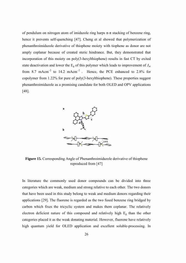
26
of pendulum on nitrogen atom of imidazole ring harps π-π stacking of benzene ring,
hence it prevents self-quenching [47]. Cheng et al showed that polymerization of
phenanthroimidazole derivative of thiophene moiety with tiophene as donor are not
amply coplanar because of created steric hindrance. But, they demonstrated that
incorporation of this moiety on poly(3-hexylthiophene) results in fast CT by exited
state deactivation and lower the Eg of this polymer which leads to improvement of Jsc
from 8.7 mAcm–2 to 14.2 mAcm–2 . Hence, the PCE enhanced to 2.8% for
copolymer from 1.22% for pure of poly(3-hexylthiophene). These properties suggest
phenanthroimidazole as a promising candidate for both OLED and OPV applications
[48].
Figure 15. Corresponding Angle of Phenanthroimidazole derivative of thiophene reproduced from [47]
In literature the commonly used donor compounds can be divided into three
categories which are weak, medium and strong relative to each other. The two donors
that have been used in this study belong to weak and medium donors regarding their
applications [29]. The fluorene is regarded as the two fused benzene ring bridged by
carbon which fixes the tricyclic system and makes them coplanar. The relatively
electron deficient nature of this compound and relatively high Eg than the other
categories placed it as the weak donating material. However, fluorene have relatively
high quantum yield for OLED application and excellent soluble-processing. In

27
addition, copolymerization with small band gap monomers creates randomLy
dispersed low energy traps that increases the probability of recombination as regards
to the type of application. On the other hand, benzodithiophene (BDT) derivatives
are regarded as medium donor because of their electron rich structure. BDT have
specific characteristic due to coplanar and rigid structure as well as symmetric
configuration, in fact, BDT derivatives have strong intermolecular π-π stacking
which is crucial for efficient CT. By considering the absorption spectrum and above
mentioned characteristics the fluorene based polymers are used for OLED and BDT
based polymer, are utilized as active layers for PV applications.
In this study, three new polymers were synthesized and their optoelectronic
properties were studied. By considering the donor-acceptor approach phenanthro-
imidazole based moieties was considered as the acceptor. There are strategies in
designing these polymers that worth to indicate. For example, alternating BDT and
electron withdrawing phenanthrene-imidazole group expected to improve electron
transfer of BDT. Beside this, it is expected introduction of this electron deficient unit
increase effective conjugation path, hence reduction in band gap. In addition to this,
in P3, 3-hexylthiophene bridge was incorporated in backbone of polymers in order to
increases the planarity of monomer. This bridge not only increase the solubility of
corresponding monomers but also results in diminishing bad gap of the polymers due
to enhancing conjugation path. Also incorporation of fluorine atom in benzene ring
expected to reduce electron density on benzene ring, hence the acceptor would be
more electron deficient. This Figure 17 shows the polymer structures that have been
studied in this work.

28
Figure 16.Structure of the Polymers.

29
CHAPTER 2
EXPERIMENTAL
2.1 Materials
The chemical reagents utilized in syntheses were supplied from Sigma-Aldrich and
Alfa Aesar and used as received. All solvents that used in reactions were freshly
distilled in the presence of benzophenone and metallic sodium. Merck Silica Gel
with 60 mesh was used for column chromatography as the stationary phase. The
synthesized chemicals were characterized by 1H and 13C Nuclear Magnetic
Resonance Spectroscopy (NMR) on Bruker Spectrospin Avance DPX-400
Spectrometer. The deuterated chloroform was used as the solvents in NMR analysis
and tetramethylsilane was the reference. All reactions were monitored by thin layer
chromatography (TLC) supplied by Merck and the products was synthesized
according to literature.
2.2 Instrumentation
2.2.1 Electrochemical Studies
In order to investigate the semiconducting properties of the polymers electrochemical
studies were performed via Voltalab 50 potentiostat. In this system ITO, platinum
and silver were working, counter and reference electrodes respectively. The solvent
was acetonitrile and the electrolyte was 0.1 M tetrabutylammonium
hexafluorophosphate (NBu4PF6) for P3. For P1 and P2 same solvent was used
whereas lithium perchlorate and sodium perchlorate (1:1 mole ratio) was used as
electrolyte. The reduction and oxidation (redox) behaviors of polymers were

30
investigated by cyclic voltammetry (CV). The electronic band gap of the polymers
was determined by measuring HOMO and LUMO. Potential of normal hydrogen
electrode to vacuum level was the reference (-4.75 V). Hence, LUMO and HOMO
were determined by HOMO= -(4.75+Eoxonset) and LUMO= -(4.75+ Eonset
red).
2.2.2 Spectroelectrochemical Studies
Spectroelectrochemical studies were conducted by Varian Cary 5000 UV– Vis
spectrophotometer to measure absorbances of natural, polaron and bipolaron states.
The polymers were coated on ITO by spray coating method. The films were oxidized
by step wise applying potential. The first absorption peaks correspond to π-π*
transitions of neutral film. The onset of maximum absorption was determined by taking
tangent line of the neutral film. Using the maximum abortion onset, the optical was
determined by converting the wavelength to electron volts. After oxidation of films by
applying step wise potential the polaron and bipolaron band emerged. The maximum
absorption of these band was determined by UV-Vis-NIR spectroscopy.
2.2.3 Kinetic Studies
In order to investigate the percent transmittance changes between the maximum
absorption of neutral and fully oxidized form of polymer in defined time interval kinetic
studies was performed. To determine the maximum abortion UV-Vis-NIR spectroscopy
was utilized. Beside this chronoamperometry was utilized to determine switching time of
the polymer films.
2.2.4 Thermal Analysis
The thermal properties of polymers were investigated by Differential Scanning
Calorimetry (DSC) and Thermogravimetric Analysis (TGA). The degradation of
polymers was investigated by TGA of Perkin Elmer Pyris 1 with rate of 10 °C/min
up to 700 °C under nitrogen atmosphere. The melting point (Tm) and glass transition
temperature (Tg) of the polymers was identified by Perkin Elmer DSC Diamond with
rate of 10 °C/min up to 300 °C under nitrogen atmosphere.
31
2.2.5 Gel Permeation Chromatography
The number and weight average molecular weight of the polymers was determined by
gel permeation chromatography (GPC). The chloroform solution of polymers (4 mg/mL)
was prepared and injected to the device. The lower molecular weight polymer would be
interacting with stationary phase, hence retarded in column. According to the size
distribution and polystyrene standard the molecular weight of polymers were
determined.
2.3 Synthesis of 2,5-dibromothiophene-3-carbaldehyde
Figure 17. Synthesis of 2,5-dibromothiophene-3-carbaldehyde
A mixture of HBr (10 mL) and bromine (6.57 g, 2.15 mL, 41.1 mM) was added to
mixture of thiophene-3-carbaldehyde (1.92 g, 17.10mmol, 1.50 mL) and diethyl ether
(15 mL) in ice cold condition. After completion of addition, the mixture was heated
to 50 °C for 14 hours. The mixture was cooled to room temperature and quenched
with saturated sodium bisulfate solution. The aqueous mixture was extracted with 40
mL diethyl ether 2 times. The organic layer was dried over sodium sulfate and
solvent was removed under reduce pressure. The crude product was purified by
means of column chromatography (hexane as the eluent) to give a pale yellow solid
(3.51g ,77%). 1H NMR (400 MHz, CDCl3) δ 9.73 (s, 1H), 7.27 (s, 1H).

32
2.8 Synthesis of 2-(2,5-dibromothiophen-3yl)-1-(4-hexylphenyl)-1H-
phenanthro[9,10-d]imidazole
Figure 18. Synthesis of 2-(2,5-dibromothiophen-3-yl)-1-(4-hexylphenyl)-1H-phenanthro[9,10-d]imidazole
A mixture of 4-hexylaniline (1.64 g, 9.26 mmol, 1.80 mL), ammonium acetate (570
mg, 7.41 mmol), phenanthrene-9,10-dione, (390 mg, 1.85 mmol) 2,5-
dibromothiophene-3-carbaldehyde, (500 mg, 1.85mmol) was charged in two neck
round-bottom flask. The flask was purged by argon for 30 min. Then acetic acid (20
mL) was added and argon was bubbled for additional 30 min. The mixture was
refluxed at 120 °C for 12 hours. After completion of reaction, the solution was
partitioned by 500 mL water and 50 mL chloroform. The organic layer was washed
with brine. The organic layer was dried over sodium sulfate and concentrated under
reduce pressure. The crude product was purified via column chromatography (1:1
hexane: dichloromethane) to obtain wheat color powder. For further purification the
powder was washed with cold methanol (60mL) to give cream color crystals (630mg,
55%) named as M2. 1H NMR (400 MHz, CDCl3) δ 8.74 (dd, J = 7.9, 1.1 Hz, 1H),
8.67 (d, J = 8.4 Hz, 1H), 8.60 (d, J = 8.2 Hz, 1H), 7.65 (dd, J = 11.0, 4.0 Hz, 1H),
7.56 (ddd, J = 8.3, 7.2, 1.4 Hz, 1H), 7.46 – 7.40 (m, 1H), 7.25 (s, 4H), 7.19 (d, J = 4.2
Hz, 2H), 6.63 (s, 1H), 2.70 – 2.64 (m, 2H), 1.64 (dd, J = 12.8, 5.8 Hz, 3H), 1.27 (s,
8H), 0.84 (t, J = 6.5 Hz, 4H).. 13C NMR (101 MHz, CDCl3) δ 143.90, 143.37,
136.27, 133.84, 131.32, 130.47, 128.81, 128.34, 127.76, 127.25, 127.03, 126.42,
126.11, 125.26, 124.69, 124.18, 123.03, 122.07, 121.73, 119.99, 118.91, 113.66,
110.10, 34.57, 30.63, 29.98, 27.77, 21.60, 13.09.

33
2.9 Synthesis of 2-(2,5-dibromothiophen-3-yl)-1-(4-fluorophenyl)-1H-
phenanthro[9,10-d]imidazole
Figure 19. Synthesis of 2-(2,5-dibromothiophen-3-yl)-1-(4-fluorophenyl)-1H-phenanthro[9,10-d]imidazole
A mixture of 4-fluoroaniline (1.00 g, 0.88 mL), ammonium acetate (580 mg, 7.50
mmol) phenanthrene-9,10-dione (390 mg,1.85 mmol), 2,5-dibromothiophene-3-
carbaldehyde (500.00 mg, 1.85 mmol) was charged in two neck round-bottom flask.
The flask was purged by argon for 30 min. Then acetic acid (20 mL) was added and
argon was bubbled for additional 30 min. The mixture was refluxed at 123 °C for 15
hours. After completion of reaction, the solution was partitioned by 500 mL water
and 50 mL chloroform. The organic layer was washed with brine. The organic layer
was dried over sodium sulfate and concentrated under reduce pressure. The grey
crude product was crystallized in hexane: dichloromethane (1:1) to give a white
powder (560 mg, 56%). 1H NMR (400 MHz, CDCl3) δ 8.72 (d, J 7.8 Hz, 1H), 8.66
(d, J = 8.3 Hz, 1H), 8.59 (d, J = 8.2 Hz, 1H), 7.68 – 7.61 (m, 1H), 7.56 (dd, J = 11.2,
4.1 Hz, 1H), 7.44 (t, J = 7.6 Hz, 1H), 7.37 – 7.30 (m, 2H), 7.26 – 7.20 (m, 1H), 7.17
– 7.08 (m, 3H), 6.69 (s, 1H). 13C NMR (101 MHz, CDCl3) δ 162.99, 160.50, 143.17,
136.19, 132.20, 130.98, 130.27, 128.96, 128.23, 127.09, 126.26, 125.77, 125.21,
124.67, 124.18, 122.99 , 121.89, 121.51, 121.32, 119.50, 115.79, 113.69, 110.45.

34
2.10 Synthesis of tributyl(4-hexylthiophen-2-yl)stannane
Figure 20. Synthesis of tributyl(4-hexylthiophen-2-yl)stannane
3-Hexylthiophene (1.00 g, 3.07 mmol) was dissolved in 20 mL anhydrous THF
under argon atmosphere. The solution was cooled to -78°C. After 30 min, n-butyl
lithium (1.5 mL, 2.5 M, 3.70 mmol) was added slowly to the solution in one hour.
The mixture was stirred at this temperature for additional one hour. Then tributylthin
chloride (0.52 mL, 3.69 mmol) was added to solution in 30 min. After 1 hour, the
mixture was brought to room temperature and stirred for 12 hours. The solvent was
removed under reduced pressure. The yellow oil was extracted by 50 Ml chloroform
and 100 mL water. Organic layer dried over sodium sulfate and concentrated under
reduce pressure. The yellow oil (1.23g, 87%) was used without purification.
2.11 Synthesis of 2-(4,4''-dihexyl-[2,2':5',2''-terthiophen]-3'-yl)-1-(4-
fluorophenyl)-1H-phenanthro[9,10-d]imidazole
Figure 21. Synthesis of 2-(4,4''-dihexyl-[2,2':5',2''-terthiophen]-3'-yl)-1-(4-fluorophenyl)-1H-phenanthro[9,10-d]imidazole
Tributyl(4-hexylthiophen-2-yl) stannane (560 mg, 1.20 mmol) and M2 (300 mg, 543
µmol) were dissolved in freshly distilled toluene. The mixture was bubbled with
argon for an hour. Then bis(triphenylphosphine)palladium(II) chloride (19.06 mg,
27.16 µmol) and tri(o-tolyl) phosphine (49.60 mg, 163 µmol) were added in one

35
portion and mixture was stirred for fifteen minutes. The well dispersed mixture was
refluxed at 120 °C for 7 hours. After completion of the coupling reaction, the
solution was concentrated under vacuum. The residue was extracted by chloroform
and organic layer was washed by brine two times. The organic layer was dried over
sodium sulfate. The crude product was purified by column chromatography (1:20
ethyl acetate: petroleum ether) to give a viscous yellow oil (225 mg, 57%).1H NMR
(400 MHz, CDCl3) δ 8.77 (dd, J 7.9, 0.9 Hz, 1H), 8.57 (t, J 8.9 Hz, 1H), 8.52 (d,
J = 8.3 Hz, 1H), 7.59 (t, J = 7.4 Hz, 1H), 7.52 – 7.43 (m, 1H), 7.32 (dt, J = 21.1, 7.0
Hz, 1H), 7.13 – 7.04 (m, 3H), 6.90 – 6.81 (m, 5H), 6.63 (s, 1H), 6.57 (d, J = 6.1 Hz,
1H), 6.51 (s, 1H), 2.42 – 2.36 (t, 2H), 2.25 (t, J = 7.6 Hz, 2H), 1.48 (ddd, J = 22.2,
11.4, 5.0 Hz, 4H), 1.33 – 1.11 (m, 14H), 1.09 – 0.92 (m, 8H), 0.85 – 0.62 (m, 11H).
2.12 Synthesis of 2-(5,5''-dibromo-4,4''-dihexyl-[2,2':5',2''-terthiophen]-3'-yl)-1-
(4-fluorophenyl)-1H-phenanthro[9,10-d]imidazole
Figure 22. Synthesis of 2-(5,5''-dibromo-4,4''-dihexyl-[2,2':5',2''-terthiophen]-3'-yl)-1-(4-fluorophenyl)-1H-phenanthro[9,10-d]imidazole
2-(4,4''-Dihexyl-[2,2':5',2''-terthiophen]-3'-yl)-1-(4-fluorophenyl)-1H-phenanthro
[9,10-d] imidazole (225 mg, 310 µmol) was dissolved in anhydrous THF. The
solution was charged in aluminum foil sealed two neck flask by syringe and NBS
(115 mg, 650 µmol) was added to solution portionwise in two hours. The reaction
was completed after 8 hours and THF was removed. The crude product was purified
by column chromatography (ethyl acetate: hexane 1:40) without extraction. The
final product was a dark yellow oil (87 mg, 32%) named as M2. 1H NMR (400 MHz,
CDCl3) δ 8.78 (d, J 6.9 Hz, 1H), 8.73 (d, J 8.3 Hz, 1H), 8.67 (d, J 8.3 Hz, 1H),

36
7.69 (t, J = 7.1 Hz, 1H), 7.62 (dd, J = 11.1, 4.2 Hz, 1H), 7.48 (t, J = 7.1 Hz, 1H), 7.23
(t, J = 7.2 Hz, 1H), 7.14 (d, J = 7.5 Hz, 1H), 7.07 – 6.98 (m, 5H), 6.77 (s, 1H), 6.56
(s, 1H), 2.49 – 2.43 (m, 2H), 2.34 – 2.29 (m, 2H), 1.56 – 1.45 (m, 4H), 1.39 – 1.17
(m, 11H), 1.08 (ddd, J = 14.5, 12.3, 7.3 Hz, 6H), 0.83 (t, J = 7.1 Hz, 3H), 0.73 (t, J =
7.0 Hz, 3H). 13C NMR (101 MHz, CDCl3) δ 145.85 – 145.37, 142.88, 137.65 –
137.12, 135.87 – 135.80, 135.36 – 135.33, 135.12, 134.06,133.95, 133.30,133.19,
129.65, 129.61,129.52, 129.43,129.33, 128.28 ,128.26, 127.37, 127.25, 127.16
,126.97, 126.55, 126.30 ,126.20, 125.75, 125.23,125.17, 124.96, 124.12, 123.05,
122.72, 122.57,122.47, 120.73, 116.55, 116.32, 110.38,110.26, 108.64,108.57, 31.40,
29.34, 28.72, 22.41, 13.96. HRMS, Mass: 885.0858, Calculated: 885.0845.
2.13 Synthesis of P1
Figure 23. Synthesis of P1
K2CO3 was dissolved in deionized water to prepare 2 M,1 mL solution. The solution
was charged in 25 mL two neck round bottom flask and purged with argon for 30
min. Under argon atmosphere in a separate flask M1(150 mg, 243 µmol) was
dissolved in freshly distilled THF. After that, 2,2’-(9,9-dioctyl-9H-fluorene-2,7-
diyl)bis(4,4,5,5-tetramethyl-1,3,2-dioxaboralane (156 mg, 243 µmol) was added to
the potassium carbonate solution, then the mixture was bubbled with argon for
further 30 min. The ammonium tetrahexyl iodide (5.00 mg, 21.0 µmol) was added to
mixture followed by purging for extra thirty minutes. After that, tris(o-
tolyl)phosphine (29.5 mg, 97.0 µmol) and tris(dibenzylideneacetone) dipalladium(0)
(11.0 mg, 12.10 µmol) was added to the solution. The polymerization reaction was
refluxed at 80 °C for 60 hours under argon atmosphere. Then 2-bromothiophene
(96.5 mmL, 970 µmol) was added to mixture followed by addition of 3 mg

37
tris(dibenzylideneacetone) dipalladium(0) and 5 mg tris(o-tolyl)phosphine . After 4
hours, other end capper thiophene-2-boronic acid pinacol ester (204 mg, 970 µmol)
was added to mixture followed by addition of 3 mg tris(dibenzylideneacetone)
dipalladium(0) and 5 mg tris(o-tolyl)phosphine. The reaction was ended after 4
hours. After cooling to room temperature THF was removed under reduce pressure.
The polymer solution was dissolved in 1 mL (0.5 mL, two times) and precipitate in
200 mL cold methanol. The precipitants were collected by vacuum filtration. For
purification of the precipitants, Soxhlett apparatus was used. The precipitates were
washed first by methanol followed by washing with acetone. The polymer was
collected with hexane. After that, the solvent was removed under reduced pressure.
The polymer was dissolved in 0.5 mL chloroform and precipitated in cold methanol.
The precipitant was collected by vacuum filtration to give 130 mg (61%) P1. GPC
results Mw: 10162, Mn :7327 PDI:1.39
2.14 Synthesis of P2
Figure 24. Synthesis of P2.
M1(160 mg, 259 µmol) was dissolved in 7 mL freshly distilled toluene under argon
atmosphere. The solution was transferred to 25 mL two necked round bottom flask
under argon. The solution was bubbled with argon for half an hour. After that, 4,8-
bis(octyloxy)benzo[1,2-b:4,5-b’] dithiophene-2,6-diyl) bis(trimethylstannane)
(200mg, 259 µmol) was added and the mixture was degassed with argon for 30 min.
Then bis(triphenylphosphine) palladium(II) chloride (9.10mg, 13 µmol) and tri(o-
tolyl) phosphine (31 mg, 103 µmol) was added followed by refluxing the solution at
120 °C for 60 hours. After completion of polymerization, 2-bromothiophene (100

38
mmL, 1.00 mmol), and additional 3 mg of bis(triphenylphosphine) palladium(II)
chloride was added to solution. After four hours, tributyl(thiophen-2-yl) stannane
(235 mmL, 1.00 mmol) was added to solution and the reaction continued for four
more hours. After cooling to room temperature the solution was concentrated under
reduced pressure. The polymer solution was dissolved in 1 mL (in 0.5 two time) and
precipitated in 200 mL cold (4-5 °C) methanol. The precipitants were filtered
collected residual purified with Soxhlet apparatus. First it was washed with methanol
followed by washing with acetone to remove the catalyst and unreacted reactants.
The oligomers were collected with hexane and the polymer was collected in
chloroform. The polymer was precipitated in methanol after concentrating of the
solution under reduced pressure to give 190mg (79%) P2. GPC results: Mw:58400
Mn: 31500. PDI: 1.86.
2.15 Synthesis of P3
Figure 25. Synthesis of P3.
M2 (87.00 mg, 98.32 µmol) was dissolved in 7 mL freshly distilled toluene under
argon atmosphere. The solution was transferred to 25 mL two necked round bottom
flask under argon. The solution was bubbled with argon for 30 min. After that, (4,8-
bis(octyloxy)benzo[1,2-b:4,5-b’] dithiophene-2,6-diyl) bis(trimethylstannane) (76
mg, 98.0 µmol) was added and bubbled for extra half an hour. Then
bis(triphenylphosphine) palladium(II) chloride (3.50 mg, 4.92 µmol) and tri(o-tolyl)
phosphine (12.0 mg, 39.0 µmol) was added followed by refluxing the solution at 120
°C for 60 hours. After completion of polymerization, 2-bromothiophene (38.0 mmL,
393 µmol) and additional 3 mg of bis(triphenylphosphine) palladium(II) chloride was
added to solution. After four hours tributyl(thiophen-2-yl) stannane (80 mmL, 394

39
µmol) was added to solution and the reaction continued for four more hours. After
cooling to room temperature the solution was concentrated under reduced pressure.
The polymer was dissolved in 1 mL (in 0.5 two times) and precipitated in 200 mL
cold (4-5 °C) methanol. The precipitants were filtered collected residuel purified
with Soxhlet apparatus. First it was washed with methanol followed by washing with
acetone to remove catalyst and unreacted reactants. The oligomers were collected in
hexane and the polymer was collected in chloroform. The polymer was precipitated
in methanol after concentrating the solution under reduced pressure. For extra
purification the collected polymer was dissolved in chloroform and 5 mg quadrazine
was added to it and stirred for 1 hour. The mixture was passed from silicon packed
column in which chloroform was solvent. The solvent was removed under reduce
pressure to give 53mg (45%) P3. GPC results: Mw:26600 Da, Mn: 16700 Da. PDI:
1.60.
2.16 Organic Photovoltaic Device Fabrication
The PV device was constructed according to the following procedure. The ITO was
etched by hydrochloric acid. The film was cleaned by successive rinsing in toluene,
distilled water with detergent, distilled water, acetone and isopropyl alcohol. For
removing any organic contaminations ozone treatment was performed for 5 min.
After cleaning the ITO, PEDOT: PSS was coated by spin coater (G3P-8) at rate of
5000 rpm. To removing solvent, the film was heated at 130 °C for 15 min. Then
chloroform was used to prepared polymer-PCBM solution. The solution passed
through 0.22 μm PTFE membrane. The solution was spin coated in a glove box. The
spinning rpm was 750 for the first 30 seconds then the rate was increased to 2500 for
40 seconds. Lithium fluoride (LiF) was (1 nm) physically evaporated on polymer in
glove box under inert atmosphere (the pressure was below 10-6 mbar and the
concentration of O2 and H2O were below 1ppm). Lastly aluminum electrode was
evaporated on top of the calcium layer by rate of 0.1 Å per second in an inert
atmosphere. The J-V charectrization of the device was investigated by Keithley SMU
236 as source in glove box via 1.5 G illuminance (100 mV/cm).

40
2.17 OLED Device Fabrication
For preparing OLED device, ITO was cleaned as mention before. The PEDOT:PSS
was coated by spin coater at a rate of 5000 rpm. To removing solvent, the film was
heated at 130 °C for 15 min. The corresponding polymer was dissolved in
chloroform and the solution was passed through 0.22 μm PTFE membrane. Then the
filtered solution spin coated on top of PEDOT:PSS at rate of 2000 rpm for 40
seconds. The LiF about 1 nm was physically evaporated in on top of polymer layer.
Lastly aluminum about 100 nm was evaporated at rate of 0.5-0.1 Å per second in
inert atmosphere.

41
CHAPTER 3
Results and discussion
3.1 Synthesis
Recent advances in organic synthesis utilizing cross coupling reaction become
driving force in field of polymer based optoelectronic applications. In this work two
monomers were synthesized and polymerized via Suzuki and Stille coupling
reactions. Firstly, thiophene-3-carbaldehyde was brominated in ice cold condition to
synthesize 2,5-dibromothiophene-3-carbaldehyde. Then, monomers were synthesized
from 2,5-dibromothiophene-3-carbaldehyde, ammonium acetate, phenanthrene-9,10-
dione and corresponding aniline (4-hexylaniline or 4-fluoroaniline) which result in
imidazole ring closure [47,48]. 4-hexylaniline containing moiety donated as
monomer 1 (M1). M1 and 2,2'-(9,9-Dioctyl-9H-fluorene-2,7-diyl)bis[4,4,5,5-
tetramethyl-1,3,2-dioxaborolane alternatingly polymerized via Suzuki
polycondensation reaction to synthesize P1. Also, M1 polymerized with 4,8-
bis(octyloxy)benzo[1,2-b:4,5-b’] dithiophene-2,6-diyl) bis(trimethylstannane) in
presence of palladium(II) catalysts to synthesize P2. However, 4-fluoroaniline
containing moiety has low solubility,hence, this moiety coupled with tributyl(4-
hexylthiophen-2-yl)stannane as bridge. This bridge not only increase the solubility
but also expected to increase the planarity and conjugation path. After coupling with
thiophene bridge, it was brominated from bridge sides to synthesize monomer 2
(M2). M2 polymerized with 4,8-bis(octyloxy)benzo[1,2-b:4,5-b’] dithiophene-2,6-
diyl) bis(trimethylstannane) via Stille coupling reaction which named as P3.

42
3.2 Cyclic voltammetry
The electronic bad gap of polymers can be determined by cyclic voltammetry.
Besides the location of HOMO and LUMO of polymers can be calculated by means
of CV. To investigate electronic properties of the polymers in thin film on ITO they
were prepared by spray coating from chloroform (5 mg/mL) solution. The
voltammetry studies were conducted in a three electrode system in which acetonitrile
and TBAPF6 were the solvent and the supporting electrolyte respectively. In this
system, polymer coated ITO was the working electrode, a platinum wire was the
counter electrode and a silver wire was the reference one. In this experiment voltage
was scanned with a rate of 100 mV/s in all cases. From results of electrochemical
studies LUMO and HOMO energy levels were calculated using onset potentials of
reduction and oxidation peaks. These calculations are shown in equations 13 and 14.
( ) Equation 13
( ) Equation 14
The cyclic voltammetry spectra of polymers are shown in Figure 28. As can seen
from Figure 28, P1 shows only oxidation potential at 1.59 V with reversible
reduction peak at 1.27 V. Likewise, P2 shows only oxidation potential at 1.20 V and
dedoping peak at 0.72 V. However, P3 shows ambipolar characteristics. The p-type
and n-type reversible oxidation and reduction pairs of P3 were observed as 1.10/0.79
V and -0.91/-0.78 V respectively.

43
Figure 26. Cyclic Voltammetry of P1, P2 and P3

44
The HOMO of polymers was measured from oxidation onset. However, the LUMO
of P1 and P2 could not be measured directly. HOMO of P1 and P2 were calculated
as -6.00 and -5.64 eV respectively. Hence, LUMO of these two polymer calculate
from Egop and HOMO. The calculated LUMO of P1 is -3.6 eV and LUMO of P2
calculate as -3.42 eV. Since P3 is - ambipolar, the band gap of polymers can be
calculated from CV directly. The measured HOMO from onset of oxidation peak is -
5.53 eV for P3. The LUMO was calculated as -3.09 eV. For P3. From difference of
HOMO and LUMO levels of corresponding polymer electronic band gap (Egec
)
calculated as 2.44 eV for P3. These results are summarized in Table 1.
Table 1. Electrochemical Characteristics of Polymers.
Ep-doping
(V)
Ep-dedoping
(V)
En-doping
(V)
En-dedoping
(V)
HOMO
(eV)
LUMO
(eV)
Egec
(ev)
P1 1.60 1.20 -6.00 -3.6
P2 1.22 0.72 -5.64 -3.42
P3 1.10 0.78 -2.03 -1.67 -5.53 -3.09 2.44
3.3 Spectroelectrochemical Studies
Spectroelectrochemical experiments were conducted to investigate the optical
properties of polymers during redox reactions. In this study, polymer films were
prepared by spray coating on ITO from polymer solution (5mg/mL in chloroform).
The films were connected to the three electrode system in which acetonitrile and
TBAPF6 were the solvent and the supporting electrolyte respectively. The
spectroelectrochemical spectra of the P3 in Uv-Vis-NIR region is depicted in Figure
29. The first absorption peak in spectrum where polymers are completely in their
neutral state correspond to π-π* transition in visible region. Upon applying potential
absorbance of neutral state of polymer depletes whereas intensities of oxidized form

45
of polymer with lower band gap known as polaron and bipolaron bands increase
(shown by arrow in the spectra). The maximum absorption in neutral state was
observed as 465 nm for P3. P3 showed maximum peaks for polaron and bipolaron
band at 740 and 1700 nm respectively. The color of P3 is red in neutral and by
oxidation the color of it changes to light grey at 1 V and fully oxidation form at 1.1 V
shows dark grey color. The reduced form of the P3 reveal marine color. The
resulting color of polymers are represented Figure 29.
Figure 27. Spectroelectrochmical Spectra of P3 and color at -2, 0, 1 and 1.1 V.
3.4 Kinetic Studies
In order to measure switching times and optical contrast of polymers between their
neutral state and oxidized state kinetic studies were performed. To do this, a potential
was applied to the polymer coated ITO film with a residence time of 5 seconds for
each cycle. During this experiment voltage was changed between 0.0-1.1V for P3 in
defined time interval and the percent transmittance was measured in visible and near
IR regions. The results are depicted in Figure 30 and the switching time and optical
contrasts are represented in Table 2. The optical contrast of P3 was measured as 8%

46
at 465 nm, 14% at 740 nm and 55% at 1700 nm. The time that is necessary to reach
95% change in transmittance during applied potential is called switching time. The
observed switching times for P3 are 3.6, 0.6 and 1.0 s at 465, 740 and 1700 nm
respectively. The reason for high switching time for polymers may be the transport
resistance of counter ion, lack of porosity of polymers and compact aggregation of
the film which prevents counter ion penetration [50].
Figure 28. Percent Transmittance Change of P3.
Table 2. Switching Times and Optical Contrast in Near IR and Visible region
Wavelength(nm) Optical
Contra t(ΔT%)
Switching
Times (s)
P3
1700 55 1.0
740 14 0.6
465 8 3.6

47
3.5 Optical Properties of Polymers
Optical properties of polymers were investigated via UV-visible absorption
spectroscopy. The measured absorption spectra of polymers are presented in Figure
31. The onset, maxima and optical band gap of the polymers are represented in
Table 3. The maxima were observed for P1, P2 and P3 as 410, 508 and 456 nm
respectively. Via incorporating a bridge to polymer back bone, it is expected to have
a lower band gap with help of increasing planarity and conjugation path. The optical
band gap of the P3 which contains thiophene bridge is smaller than P1 and P2 as
expected.

48
Figure 29. Uv-Visible Absorption Spectra of the Polymers (P1, P2 and P3) in chloroform Solution and thin film.
Table 3. Optical Properties of Polymer.
λmax (nm) λmaxonset
(nm) Eg op
(eV)
P1 410 520 2.40
P2 508 560 2.22
P3 465 568 2.18
3.6 Thermal Analysis of Polymers
The thermal properties of polymers were investigated by DSC and TGA. The TGA
results show glass transition of P1 at 128 °C and for P2 the glass transition could not
be determined which can be attributed to the rigidity of polymer structure. The DSC
results show that P1 weight loss of 48% at 430 °C and continue to weight loss of
53% until 657 °C. P2 is stable up to 320 °C and weight loss of 38.4% is seen until
700 °C. (All results are in Appendix B).

49
3.7 Polymer Light Emitting Diode Application of P1
In this study OLED properties of P1 was investigated. The luminescence of polymer
was investigated through photoluminescence and electroluminescenec. In order to
study the photoluminescence characteristics both solution and thin film were excited
at corresponding maximum absorptions. The maximum emission of the polymer in
chloroform solution was 425 nm and 485 nm in thin film (Figure 32). The red shift
in thin film can be explained by the stacking of molecules and lower degree of
freedom in compare to those in solution.
Figure 30. Photoluminescence of P1 in chloroform solution and thin film.
In order to measure electroluminescenec and current density-luminesce-voltage
characteristics (JLV) of a single layer device with ITO/PEDOT:PSS/P1/LiF/Al
structure was constructed. The device has a turn on voltage of 11 V with a
luminescence of 210 cd/m2 and represents maximum luminescence of 5627 cd/m2 at
13V and 1267 mA/cm2 as given in Figure 33. The electroluminescenec spectrum of
the polymer is shown in Figure 34 which indicated maximum emission at 476 nm.
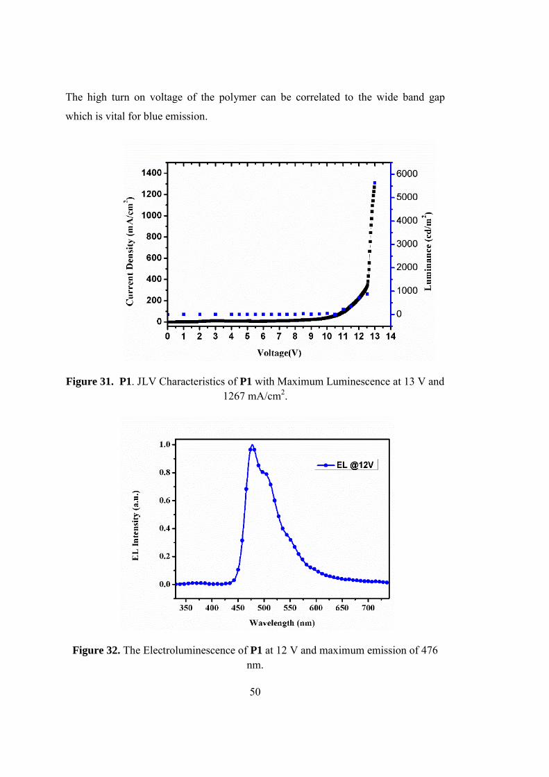
50
The high turn on voltage of the polymer can be correlated to the wide band gap
which is vital for blue emission.
Figure 31. P1. JLV Characteristics of P1 with Maximum Luminescence at 13 V and 1267 mA/cm2.
Figure 32. The Electroluminescence of P1 at 12 V and maximum emission of 476 nm.

51
The CIE coordinates of the emitted light were recorded as x=0.187,y=0.369 which
correspond to greenish-blue color as seen in Figure 35.
Figure 33. Color Coordinates of Emitted Light by P1.
3.8 Organic Photovoltaic Application
The photovoltaic properties of P2 and P3 were investigated with a device structure of
ITO/PEDOT:PSS/Polymer:PCBM/LiF/Al under AM 1.5 condition in an inert
atmosphere. The corresponding polymer was mixed with different ratios of PCBM to
optimize active layer. The optimization results of polymer are represented in Table
4. The J-V characteristics of P2 and P3 are depicted in Figure 36. The best result
for P2 device was the 1:3 ratio of the polymer and PCBM with PCE of 0.94 % and
31% fill factor. The corresponding short current density and open circuit voltage of
the d evice were measured as 5.62 mA/cm2 and 0.54 V. The highest efficiency of P3
was measured as 0.91% with 1:2 ratio of polymer:PCBM. The Jsc , Voc and fill factor
of P3 device in this configuration were found as 4.48 mA/cm2, 0.58 V and 35%
respectivly. Although the open circuit voltages of the two polymers are all most
same, P2 shows 0.03% which can be attributed to higher short current density. On

52
the other hand, P3 shows a fill factor of 35% which means the hole and electron
transfer in this device amore efficient than P2.
Figure 34. J-V characteristics of P2 and P3

53
Table 4. Optimization Studies of P2 and P3 for OPVs.
P2:PCBM VOC
(V)
JSC
(mA/cm2)
Vmax
(V)
Jmax
(mA/cm2)
FF
(%)
PCE (%)
1:1 0.52 3.19 0.28 1.68 28 0.47
1:2 0.53 4.42 0.32 2.39 33 0.77
P2 1:3 0.54 5.62 0.30 3.16 31 0.94
1:4 0.52 4.61 0.29 2.79 34 0.82
1:1 0.57 3.49 0.33 2.04 34 0.67
P3 1:2 0.58 4.48 0.35 2.62 35 0.91
1:3 0.57 3.13 0.34 1.82 35 0.62

54

55
CHAPTER 4
Conclusion
Three new conjugated polymers based on phenanthro-imidazole were synthesized via
Suzuki and Stille coupling polycondensation reactions. These polymers were utilized
as an active layer for organic photovoltaic and organic light emitting diode
applications. Cyclic voltammetry, spectroelectrochemical and kinetic studies was
conducted to investigate electrochromic and electrochemical properties of polymers.
Electrochemical studies reveal that P3 has ambipolar character with band gap of 2.44
eV. The optical band gap of the polymers were determined as 2.40, 2.22 and 2.18 eV
for P1, P2 and P3 respectively. Kinetic studies represent P3 could be promising
candidate for near IR electrochromic devices due to its 55% optical contrast at 1700
nm with 1s switching time. P1 shows a maximum luminescence of 5627 cd/m2 at
13V and turn on voltage of 11V. The color coordination of CIE diagram was
x=0.187, y=0.369 indicating cyan color. For P2 and P3 device optimizations were
performed according to polymer and PC71BM ratios. The optimized device of P2
shows PCE of 0.94% , Voc of 0.54V, Jsc of 5.63 mA/cm2 and Fill Factor (FF) of 31%.
The best performance of P3 based device represent a PCE of 0.91%, Voc of 0.58V, Jsc of
4.48 mA/cm2 and Fill Factor (FF) of 35%.

56

57
REFERENCES
[1] M.A.Green, K.Emery, Y.Hishikawa, W.Warta, E.D.Dunlop, Prog. Photov.
Res. Appl. 24 (2016) 905–013.
[2] P. Chapin, M, Fuller, C, G, J. Appl. Phys. 25 (1954) 675-682.
[3] V.C. Sundar, J. Zaumseil, V. Podzorov, E. Menard, R.L. Willett, T. Someya,
M.E. Gershenson, J. A. Rogers, Science. 303 (2004) 1644–1646.
[4] W. Hu, Organic Electronics II Organic Photovoltaics Physics of Organic
Semiconductors Physical and Chemical Aspects of Organic Electronics (2012)
526-527.
[5] J. Zhao, Y. Li, G. Yang, K. Jiang, H. Lin, H. Ade, W. Ma, H. Yan, Nat.
Energy 1 (2016) 15027-15034.
[6] O.A. Abdulrazzaq, V. Saini, S. Bourdo, E. Dervishi, A.S. Biris, Part. Sci.
Technol. 31 (2013) 427–442.
[7] S. Kappaun, C. Slugovc, E.J.W. List, Int. J. Mol. Sci. 9 (2008) 1527–1547.
[8] J.H. Burroughes, D.D.C. Bradley, A.R. Brown, R.N. Marks, K. Mackay, R.H.
Friend, P.L. Burns, A.B. Holmes, Nature 347 (1990) 539–541.
[9] W.M. Kline, R.G. Lorenzini, G.A. Sotzing, Color. Technol. 130 (2014) 73–80.
[10] D. Rosseinsky, R.J. Mortimer, Adv. Mater 13 (2001) 783–793.
[11] S.K. Deb, Appl. Opt. 8 (1969) 192-195.
[12] R.J. Mortimer, Electrochim. Acta 44 (1999) 2971–2981.
[13] A.A. Argun, P.H. Aubert, B.C. Thompson, I. Schwendeman, C.L. Gaupp, J.
Hwang, N.J. Pinto, D.B. Tanner, A.G. MacDiarmid, J.R. Reynolds, Chem.
Mater. 16 (2004) 4401–4412.
[14] S. Sindhu, K. Narasimha Rao, S. Ahuja, A. Kumar, E.S.R. Gopal, Mater. Sci.

58
Eng. B Solid-State Mater. Adv. Technol. 132 (2006) 39–42.
[15] G. Sonmez, H. Meng, F. Wudl, Chem. Mater. 16 (2004) 574–580.
[16] H. Shirakawa, E.J. Louis, A.G. MacDiarmid, C.K. Chiang, A.J. Heeger, J.
Chem. Soc. Chem. Commun. (1977) 578–580.
[17] J. Bredas, G. Street, Acc. Chem. Res. 1305 (1985) 309–315.
[18] H. Winokur, M, Moon, Y, Heeger, Barker, J, Bott, D , Shirakawa, Phys. Rev.
Lett. 59 (1987) 608-611.
[19] Y.-W.P. D. Moses, J. Chen, A. Denenstein, M. Kaveh, T.-C. Chung, A.J.
Heeger, A.G. MacDiarmid, Solid State Commun. 40 (1981) 1007–1010.
[20] D. Jacquemin, C. Adamo, J. Chem. Theory Comput. 7 (2011) 369–376.
[21] P. von R. Schleyer, Chem. Rev. 101 (2001) 1115-1117.
[22] J. Roncali, Macromol. Rapid Commun. 28 (2007) 1761–1775.
[23] C. Liu, K. Wang, X. Gong, A.J. Heeger, Chem. Soc. Rev. (2016) 4825 -4846.
[24] S.Y. Leblebici, T.L. Chen, P. Olalde-Velasco, W. Yang, B. Ma, ACS Appl.
Mater. Interfaces 5 (2013) 10105–10110.
[25] O. V Mikhnenko, P.W.M. Blom, T.-Q. Nguyen, Energy Environ. Sci. 8 (2015)
1867–1888.
[26] K. Feron, W.J. Belcher, C.J. Fell, P.C. Dastoor, Int. J. Mol. Sci. 13 (2012)
17019–17047.
[27] V.D. Mihailetchi, H. Xie, B. De Boer, L.J.A. Koster, P.W.M. Blom, Adv.
Func. Mater. 16 (2006) 699–708.
[28] M. Kuik, G.-J. a H. Wetzelaer, H.T. Nicolai, N.I. Craciun, D.M. De Leeuw,
P.W.M. Blom, Adv. Mater. 26 (2014) 512–31.
[29] Z. Zhang, J. Wang, J. Mater. Chem. 22 (2012) 4178.
[30] L. Lu, T. Zheng, Q. Wu, A.M. Schneider, D. Zhao, L. Yu, Chem. Rev. 115

59
(2015) 12666–12731.
[31] M.C. Scharber, N.S. Sariciftci, Prog. Polym. Sci. 38 (2013) 1929–1940.
[32] E. Bundgaard, F.C. Krebs, Sol. En. Mater. Sol. Cells 91 (2007) 954–985.
[33] L. Dou, Y. Liu, Z. Hong, G. Li, Y. Yang, Chem. Rev. 115 (2015) 12633–
12665.
[34] S.R. Forrest, MRS Bull. 30 (2005) 28–32.
[35] C. Brabec, V. Dyakonov, U. Scherf, Organic Photovoltaics: Materials, Device
Physics, and Manufacturing Technologies, 2009.
[36] M.C. Scharber, D. Mühlbacher, M. Koppe, P. Denk, C. Waldauf, A.J. Heeger,
C.J. Brabec, Adv. Mater. 18 (2006) 789–794.
[37] H. Li, M. Fang, Y. Hou, R. Tang, Y. Yang, C. Zhong, Q. Li, Z. Li, ACS Appl.
Mater. Interfaces (2016) 12134-12140.
[38] J. Hou, T.L. Chen, S. Zhang, L. Huo, S. Sista, Y. Yang, Macromolecules 42
(2009) 9217–9219.
[39] B. Qi, J. Wang, J. Mater. Chem. 22 (2012) 24315.
[40] N.K. Elumalai, A. Uddin, Energy Environ. Sci. 9 (2016) 391–410.
[41] D. Gupta, S. Mukhopadhyay, K.S. Narayan, Sol. En. Mater. Sol. Cells 94
(2010) 1309–1313.
[42] Y.-L. Chang, Efficient Organic Light-Emitting Diodes (OLEDs), 2016.
[43] N.H. Kim, Y.H. Kim, J.A. Yoon, S.Y. Lee, D.H. Ryu, R. Wood, C.B. Moon,
W.Y. Kim, J. Lumin. 143 (2013) 723–728.
[44] N. Thejo Kalyani, S.J. Dhoble, Renew. Sustain. Energy Rev. 16 (2012) 2696–
2723.
[45] W. Brutting, J. Frischeisen, T.D. Schmidt, B.J. Scholz, C. Mayr, Phys. Status
Solid Appl. Mater. Sci. 210 (2013) 44–65.

60
[46] E. Efstathios, Green Energy and Technology, 2006.
[47] Y. Zhang, S.-L. Lai, Q.-X. Tong, M.-Y. Chan, T.-W. Ng, Z.-C. Wen, G.-Q.
Zhang, S.-T. Lee, H.-L. Kwong, C.-S. Lee, J. Mater. Chem. 21 (2011) 8206-
8214.
[48] Y. Te Chang, S.L. Hsu, M.H. Su, K.H. Wei, Adv. Func. Mater. 17 (2007)
3326–3331.
[49] P. Cheng, Y. Li, X. Zhan, Energy Environ. Sci. 7 (2014) 2005 1351-1356.
[50] Z. Shi, W.T. Neo, T.T. Lin, H. Zhou, J. Xu, RSC Adv. 5 (2015) 96328–96335.

61
Appendix A
NMR RESULTS
Figure 35. 1H NMR of 2,5-dibromothiophene-3-carbaldehyde
Figure 36. 1H NMR of 2-(2,5-dibromothiophen-3-yl)-1-(4-hexylphenyl)-1H-
phenanthro[9,10-d]imidazole
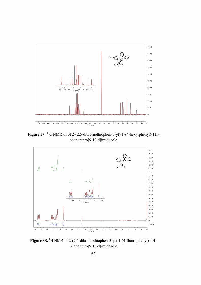
62
Figure 37. 13C NMR of of 2-(2,5-dibromothiophen-3-yl)-1-(4-hexylphenyl)-1H-
phenanthro[9,10-d]imidazole
Figure 38. 1H NMR of 2-(2,5-dibromothiophen-3-yl)-1-(4-fluorophenyl)-1H-phenanthro[9,10-d]imidazole

63
Figure 39. 13C NMR of of 2-(2,5-dibromothiophen-3-yl)-1-(4-fluorophenyl)-1H-
phenanthro[9,10-d]imidazole
Figure 40. 1H NMR of 2-(4,4''-dihexyl-[2,2':5',2''-terthiophen]-3'-yl)-1-(4-fluorophenyl)-1H-phenanthro[9,10-d]imidazole

64
Figure 41. 1H NMR of 2-(5,5''-dibromo-4,4''-dihexyl-[2,2':5',2''-terthiophen]-3'-yl)-1-(4-fluorophenyl)-1H-phenanthro[9,10-d]imidazole
Figure 42. 13C NMR of 2-(5,5''-dibromo-4,4''-dihexyl-[2,2':5',2''-terthiophen]-3'-yl)-1-(4-fluorophenyl)-1H-phenanthro[9,10-d]imidazole.

65
Figure 43. 1H NMR of P1.
Figure 44. 1H NMR of P2.

66
Figure 45. 1H NMR of P3.

67
Appendix B
Thermal Analysis Results
Figure 46. DSC Thermogram of P1.
Figure 47. DSC Themogram of P2.

68
Figure 48. TGA Curve of P1.
Figure 49. TGA Curve of P2.